Embed Size (px)
Citation preview
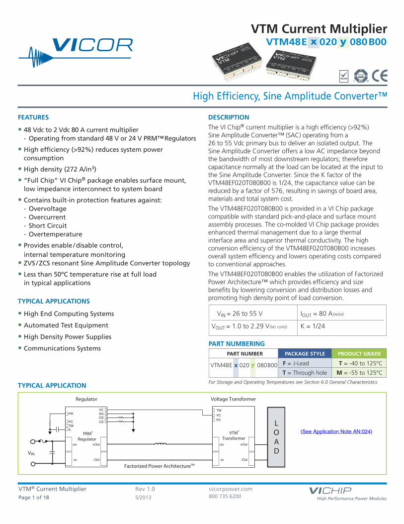
VTM® Current Multiplier Rev 1.0 vicorpower.comPage 1 of 18 5/2013 800 735.6200
High Efficiency, Sine Amplitude Converter™
S
NRTLC US
VTM Current Multiplier 020 080 B00 yE 48 VTM x
FEATURES
• 48 Vdc to 2 Vdc 80 A current multiplier- Operating from standard 48 V or 24 V PRM™Regulators
• High efficiency (> 92 %) reduces system power consumption
• High density ( 272 A /in3)• “ Full Chip ” VI Chip® package enables surface mount,low impedance interconnect to system board
• Contains built-in protection features against:- Overvoltage - Overcurrent - Short Circuit - Overtemperature
• Provides enable /disable control, internal temperature monitoring
• ZVS / ZCS resonant Sine Amplitude Converter topology• Less than 50ºC temperature rise at full load in typical applications
TYPICAL APPLICATIONS
• High End Computing Systems
• Automated Test Equipment
• High Density Power Supplies
• Communications Systems
DESCRIPTION
The VI Chip® current multiplier is a high efficiency (> 92 %) Sine Amplitude Converter™ (SAC) operating from a 26 to 55 Vdc primary bus to deliver an isolated output. The Sine Amplitude Converter offers a low AC impedance beyondthe bandwidth of most downstream regulators; thereforecapacitance normally at the load can be located at the input tothe Sine Amplitude Converter. Since the K factor of the VTM48EF020T080B00 is 1/24 , the capacitance value can bereduced by a factor of 576 , resulting in savings of board area,materials and total system cost.
The VTM48EF020T080B00 is provided in a VI Chip packagecompatible with standard pick-and-place and surface mountassembly processes. The co-molded VI Chip package providesenhanced thermal management due to a large thermalinterface area and superior thermal conductivity. The highconversion efficiency of the VTM48EF020T080B00 increasesoverall system efficiency and lowers operating costs comparedto conventional approaches.
The VTM48EF020T080B00 enables the utilization of FactorizedPower Architecture™ which provides efficiency and sizebenefits by lowering conversion and distribution losses andpromoting high density point of load conversion.
VIN = 26 to 55 V
VOUT = 1.0 to 2.29 V(NO LOAD)
IOUT = 80 A(NOM)
K = 1/24
VIN
LOAD
PR
PC
VC
TMIL
OSSG
PRM®
Regulator
CD
-Out
+Out
-In
+In
PCVCTM
-Out
+Out
-In
+In
Regulator Voltage Transformer
Factorized Power ArchitectureTM
VTM®
Transformer (See Application Note AN:024)
PART NUMBER PACKAGE STYLE PRODUCT GRADE
F = J-Lead T = -40 to 125°C
T = Through hole M = -55 to 125°C
PART NUMBERING
For Storage and Operating Temperatures see Section 6.0 General Characteristics
020 x y 080 B00 E 48 VTM
TYPICAL APPLICATION
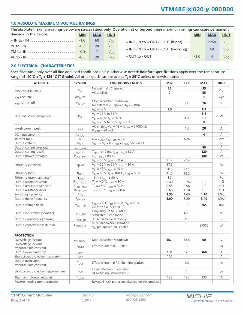
VTM® Current Multiplier Rev 1.0 vicorpower.comPage 2 of 18 5/2013 800 735.6200
020 080 B00 yE 48 VTM x
ATTRIBUTE SYMBOL CONDITIONS / NOTES MIN TYP MAX UNIT
Input voltage range VINNo external VC applied 26 55
VDCVC applied 0 55 VIN slew rate dVIN /dt 1 V/µs
VIN UV turn off VIN_UVModule latched shutdown,
24 26 VNo external VC applied, IOUT = 80 A
No Load power dissipation PNL
VIN = 48 V 1.5 8.7
WVIN = 26 V to 55 V 9.5 VIN = 48 V, TC = 25 ºC 4.2 5.7 VIN = 26 V to 55 V, TC = 2 ºC 8
Inrush current peak IINRPVC enable, VIN = 48 V, COUT = 27000 µF, 10 20 ARLOAD = 24 mΩ
DC input current IIN_DC 4 ATransfer ratio K K = VOUT/ VIN, IOUT = 0 A 1/24 V/VOutput voltage VOUT VOUT = VIN • K - IOUT • ROUT, Section 11 VOutput current (average) IOUT_AVG 80 AOutput current (peak) IOUT_PK TPEAK < 10 ms, IOUT_AVG ≤ 80 A 120 AOutput power (average) POUT_AVG IOUT_AVG ≤ 80 A 300 W
VIN = 48 V, IOUT = 80 A 91.2 92.4
Efficiency (ambient) hAMB VIN = 26 V to 55 V, IOUT = 80 A 87.3 %VIN = 48 V, IOUT = 40 A 90.5 92.1
Efficiency (hot) hHOT VIN = 48 V, TC = 100°C, IOUT = 80 A 91.2 92.2 %
Efficiency (over load range) h20% 16 A < IOUT < 80 A 80 %Output resistance (cold) ROUT_COLD TC = -40°C, IOUT = 80 A 0.40 0.76 1.0 mΩOutput resistance (ambient) ROUT_AMB TC = 25°C, IOUT = 80 A 0.55 0.98 1.2 mΩOutput resistance (hot) ROUT_HOT TC = 100°C, IOUT = 80 A 0.65 1.18 1.5 mΩSwitching frequency FSW 1.50 1.60 1.70 MHzOutput ripple frequency FSW_RP 3.00 3.20 3.40 MHz
Output voltage ripple VOUT_PPCOUT = 0 F, IOUT = 80 A, VIN = 48 V,
150 265 mV20 MHz BW, Section 12
Output inductance (parasitic) LOUT_PARFrequency up to 30 MHz,
600 pHSimulated J-lead model
Output capacitance (internal) COUT_INT Effective Value at 2 VOUT 310 µF
Output capacitance (external) COUT_EXTVTM Standalone Operation.
27000 µFVIN pre-applied, VC enable
PROTECTIONOvervoltage lockout VIN_OVLO+ Module latched shutdown 55.1 58.5 60 VOvervoltage lockout
TOVLO Effective internal RC filter 8 µsresponse time constantOutput overcurrent trip IOCP 100 120 160 AShort circuit protection trip current ISCP 160 AOutput overcurrent
TOCP Effective internal RC filter (Integrative). 4.3 msresponse time constant
Short circuit protection response time TSCPFrom detection to cessation
1 µsof switching (Instantaneous)
Thermal shutdown setpoint TJ_OTP 125 130 135 ºCReverse inrush current protection Reverse Inrush protection disabled for this product.
1.0 ABSOLUTE MAXIMUM VOLTAGE RATINGS
The absolute maximum ratings below are stress ratings only. Operation at or beyond these maximum ratings can cause permanentdamage to the device.
2.0 ELECTRICAL CHARACTERISTICS
Specifications apply over all line and load conditions unless otherwise noted; Boldface specifications apply over the temperaturerange of -40°C < TJ < 125 °C (T-Grade); All other specifications are at TJ = 25ºC unless otherwise noted.
MIN MAX UNIT
+ IN to - IN . . . . . . . . . . . . . . . . . . . . . . . -1.0 60 VDC
PC to - IN . . . . . . . . . . . . . . . . . . . . . . . . -0.3 20 VDC
TM to -IN . . . . . . . . . . . . . . . . . . . . . . . . -0.3 7 VDC
VC to - IN . . . . . . . . . . . . . . . . . . . . . . . . -0.3 20 VDC
MIN MAX UNIT
+ IN / - IN to + OUT / - OUT (hipot)........ 2250 VDC
+ IN / - IN to + OUT / - OUT (working)... 60 VDC
+ OUT to - OUT....................................... -1.0 4 VDC

VTM® Current Multiplier Rev 1.0 vicorpower.comPage 3 of 18 5/2013 800 735.6200
020 080 B00 yE 48 VTM x
SIGNAL TYPE STATE ATTRIBUTE SYMBOL CONDITIONS / NOTES MIN TYP MAX UNIT
External VC voltage VVC_EXTRequired for start up, and operation
11.5 16.5 Vbelow 26 V. See Section 7.VC = 11.5 V, VIN = 0 V 95 150
VC current draw IVCVC = 11.5 V, VIN > 26 V 9
mAVC = 16.5 V, VIN > 26 V 75 Steady
Fault mode. VC > 11.5 V 60
ANALOG
VC internal diode rating DVC_INT 100 V
INPUTVC internal resistor RVC-INT 2 kΩVC internal resistor TVC_COEFF 900 ppm/°Ctemperature coefficient
Start UpVC start up pulse VVC_SP Tpeak <18 ms 20 VVC slew rate dVC/dt Required for proper start up; 0.02 0.25 V/µsVC inrush current IINR_VC VC = 16.5 V, dVC/dt = 0.25 V/µs 1 A
VC to VOUT turn-on delay TONVIN pre-applied, PC floating, 500 µsVC enable, CPC = 0 µF
Transitional VC to PC delay Tvc_pcVC = 11.5 V to PC high, VIN = 0 V, 75 125 µsdVC/dt = 0.25 V/µs
Internal VC capacitance CVC_INT VC = 0 V 3.2 µF
• Used to wake up powertrain circuit.• A minimum of 11.5 V must be applied indefinitely for VIN < 26 V
to ensure normal operation.• VC slew rate must be within range for a succesful start.
• PRM® VC can be used as valid wake-up signal source.• Internal Resistance used in “Adaptive Loop” compensation• VC voltage may be continuously applied
VTM CONTROL : VC
3.0 SIGNAL CHARACTERISTICS
Specifications apply over all line and load conditions unless otherwise noted; Boldface specifications apply over thetemperaturerange of -40°C < TJ < 125°C (T-Grade); All other specifications are at TJ = 25°C unless otherwise noted.
SIGNAL TYPE STATE ATTRIBUTE SYMBOL CONDITIONS / NOTES MIN TYP MAX UNIT
PC voltage VPC 4.7 5 5.3 V
ANALOGSteady PC source current IPC_OP 2 mA
OUTPUTPC resistance (internal) RPC_INT Internal pull down resistor 50 150 400 kΩ
Start UpPC source current IPC_EN 50 100 300 µAPC capacitance (internal) CPC_INT Section 7 1000 pFPC resistance (external) RPC_S 60 kΩ
Enable PC voltage VPC_EN 2 2.5 3 V
DIGITALDisable
PC voltage (disable) VPC_DIS 2 V
INPUT / OUPUTPC pull down current IPC_PD 5.1 mA
TransitionalPC disable time TPC_DIS_T 5 µsPC fault response time TFR_PC From fault to PC = 2 V 100 µs
• The PC pin enables and disables the VTM. When held below 2 V, the VTM will be disabled.
• PC pin outputs 5 V during normal operation. PC pin is equal to 2.5 V during fault mode given VIN > 26 V or VC > 11.5 V.
• After successful start up and under no fault condition, PC can be used asa 5 V regulated voltage source with a 2 mA maximum current.
• Module will shutdown when pulled low with an impedanceless than 400 Ω.
• In an array of VTMs, connect PC pin to synchronize start up.• PC pin cannot sink current and will not disable other modules
during fault mode.
PRIMARY CONTROL : PC

VTM® Current Multiplier Rev 1.0 vicorpower.comPage 4 of 18 5/2013 800 735.6200
020 080 B00 yE 48 VTM x
SIGNAL TYPE STATE ATTRIBUTE SYMBOL CONDITIONS / NOTES MIN TYP MAX UNIT
TM voltage VTM_AMB TJ controller = 27°C 2.95 3.00 3.05 V
ANALOGTM source current ITM 100 µA
OUTPUT Steady TM gain ATM 10 mV/°C
TM voltage ripple VTM_PPCTM = 0 F, VIN = 48 V,
120 200 mVIOUT = 80 A
Disable TM voltage VTM_DIS 0 V
DIGITAL OUTPUT TM resistance (internal) RTM_INT Internal pull down resistor 25 40 50 kΩTransitional TM capacitance (external) CTM_EXT 50 pF(FAULT FLAG)
TM fault response time TFR_TM From fault to TM = 1.5 V 10 µs
• The TM pin monitors the internal temperature of the VTM® controller ICwithin an accuracy of ±5°C.
• Can be used as a "Power Good" flag to verify that the VTM is operating.
• The TM pin has a room temperature setpoint of 3 V and approximate gain of 10 mV/°C.
• Output drives Temperature Shutdown comparator
TEMPERATURE MONITOR : TM
4.0 TIMING DIAGRAM
1 2
7
VIN
1. Initiated VC pulse2. Controller start3. VIN ramp up4. VIN = VOVLO5. VIN ramp down no VC pulse6. Overcurrent7. Start up on short circuit8. PC driven low
VOUT
PC
3 V
VC
NL
5 V
VOVLO
TMVTM-AMB
c
Notes: – Timing and voltage is not to scale – Error pulse width is load dependent
a: VC slew rate (dVC/dt) b: Minimum VC pulse ratec: TOVLO
d: TOCP
e: Output turn on delay (TON)f: PC disable time (TPC_DIS_T)g: VC to PC delay (TVC_PC)
d
ISSP
IOUT
IOCP
VVC-EXT
3 4 5
6
a
b
8
g
e f
≥ 26 V
VTM® Current Multiplier Rev 1.0 vicorpower.comPage 5 of 18 5/2013 800 735.6200
020 080 B00 yE 48 VTM x
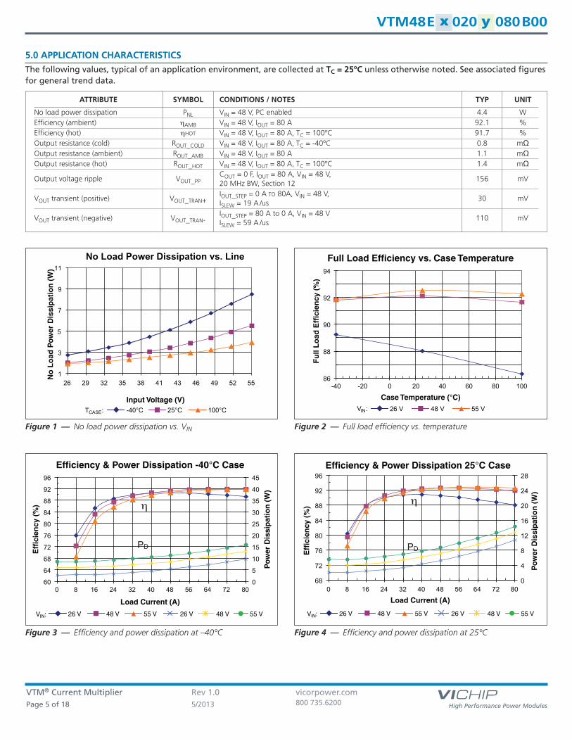
5.0 APPLICATION CHARACTERISTICS
The following values, typical of an application environment, are collected at TC = 25ºC unless otherwise noted. See associated figuresfor general trend data.
ATTRIBUTE SYMBOL CONDITIONS / NOTES TYP UNIT
No load power dissipation PNL VIN = 48 V, PC enabled 4.4 WEfficiency (ambient) hAMB VIN = 48 V, IOUT = 80 A 92.1 %Efficiency (hot) hHOT VIN = 48 V, IOUT = 80 A, TC = 100ºC 91.7 %Output resistance (cold) ROUT_COLD VIN = 48 V, IOUT = 80 A, TC = -40ºC 0.8 mΩOutput resistance (ambient) ROUT_AMB VIN = 48 V, IOUT = 80 A 1.1 mΩOutput resistance (hot) ROUT_HOT VIN = 48 V, IOUT = 80 A, TC = 100ºC 1.4 mΩOutput voltage ripple VOUT_PP
COUT = 0 F, IOUT = 80 A, VIN = 48 V, 156 mV
20 MHz BW, Section 12
VOUT transient (positive) VOUT_TRAN+IOUT_STEP = 0 A TO 80 A, VIN = 48 V,
30 mVISLEW = 19 A /us
VOUT transient (negative) VOUT_TRAN-IOUT_STEP = 80 A to 0 A, VIN = 48 V
110 mVISLEW = 59 A /us
1
3
5
7
9
11
26 29 32 35 38 41 43 46 49 52 55
Input Voltage (V)
No
Lo
ad P
ow
er D
issi
pat
ion
(W
)
-40°C 25°C 100°CT :CASE
No Load Power Dissipation vs. Line Full Load Efficiency vs. Case Temperature
Case Temperature (°C)
Fu
ll L
oad
Eff
icie
ncy
(%
)
26 V 48 V 55 VV :IN
86
88
90
92
94
-40 -20 0 20 40 60 80 100
Efficiency & Power Dissipation -40°C Case
Load Current (A)
Eff
icie
ncy
(%
)
26 V 48 V 55 VV :IN 26 V 48 V 55 V
Po
wer
Dis
sip
atio
n (
W)
PD
η
0
5
10
15
20
25
30
35
40
45
60
64
68
72
76
80
84
88
92
96
0 8 16 24 32 40 48 56 64 72 80
Efficiency & Power Dissipation 25°C Case
Load Current (A)
Eff
icie
ncy
(%
)
26 V 48 V 55 VV :IN 26 V 48 V 55 V
Po
wer
Dis
sip
atio
n (
W)
η
PD
0
4
8
12
16
20
24
28
68
72
76
80
84
88
92
96
0 8 16 24 32 40 48 56 64 72 80
Figure 1 — No load power dissipation vs. VIN Figure 2 — Full load efficiency vs. temperature
Figure 3 — Efficiency and power dissipation at –40°C Figure 4 — Efficiency and power dissipation at 25°C
VTM® Current Multiplier Rev 1.0 vicorpower.comPage 6 of 18 5/2013 800 735.6200
020 080 B00 yE 48 VTM x
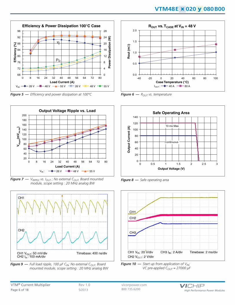
Figure 10 — Start up from application of VIN; VC pre-applied COUT = 27000 µF
Safe Operating Area
Output Voltage (V)
Out
put C
urre
nt (A
)
0
20
40
60
80
100
120
140
0 0.5 1 1.5 2 2.5 3
10 ms Max
Continuous
Figure 8 — Safe operating area
Figure 9 — Full load ripple, 100 µF CIN; No external COUT. Board mounted module, scope setting : 20 MHz analog BW
Load Current (A)
26 V 48 V 55 VV :IN
Output Voltage Ripple vs. Load
20
40
60
80
100
120
140
160
180
200
0 8 16 24 32 40 48 56 64 72 80
VR
ipp
le(m
VP
K-P
K)
Figure 7 — VRIPPLE vs. IOUT ; No external COUT. Board mounted module, scope setting : 20 MHz analog BW
Efficiency & Power Dissipation 100°C Case
Load Current (A)
Eff
icie
ncy
(%
)
26 V 48 V 55 VV :IN 26 V 48 V 55 V
Po
wer
Dis
sip
atio
n (
W)
PD
η
0
4
8
12
16
20
24
28
68
72
76
80
84
88
92
96
0 8 16 24 32 40 48 56 64 72 80
ROUT vs. TCASE at VIN = 48 V
Case Temperature (°C)
Ro
ut
(mΩ
)
I :OUT 40 A 80 A
0.0
0.5
1.0
1.5
2.0
-40 -20 0 20 40 60 80 100
Figure 5 — Efficiency and power dissipation at 100°C Figure 6 — ROUT vs. temperature
VTM® Current Multiplier Rev 1.0 vicorpower.comPage 7 of 18 5/2013 800 735.6200
020 080 B00 yE 48 VTM x
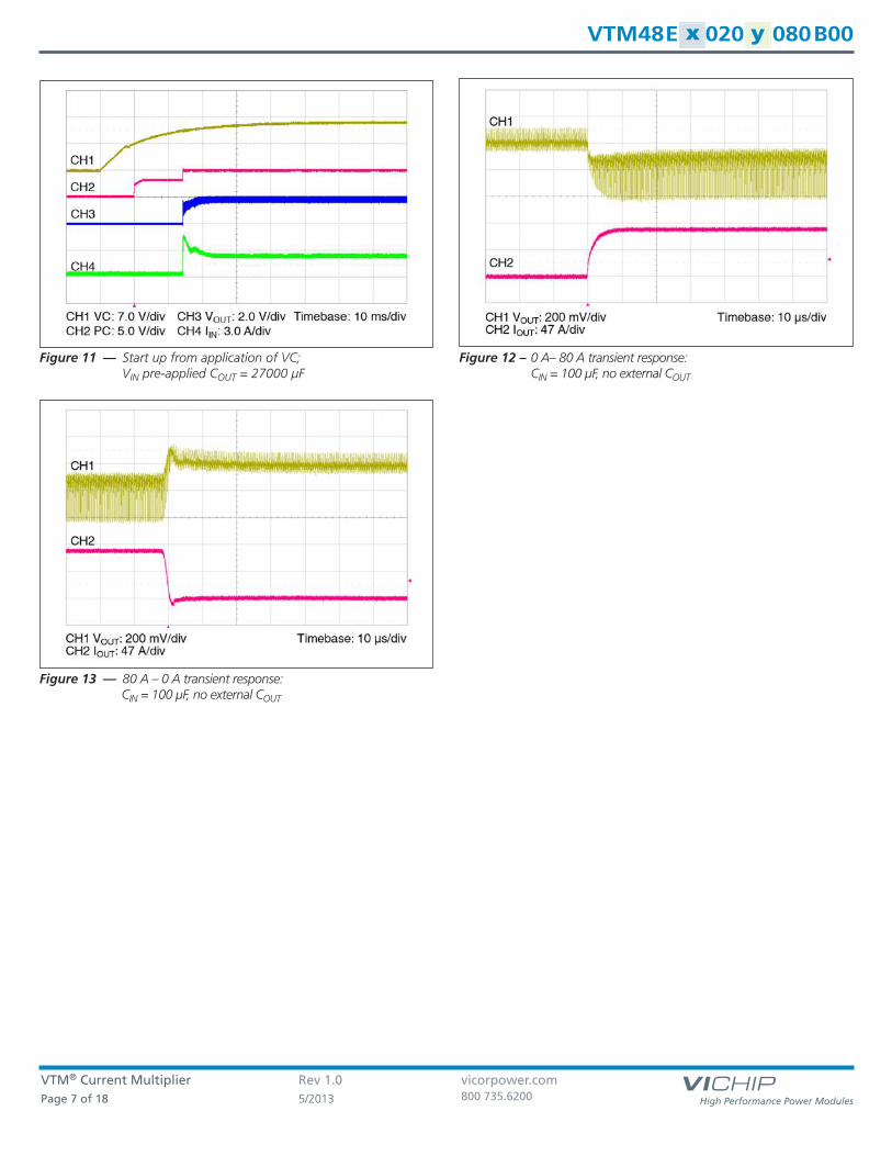
Figure 13 — 80 A – 0 A transient response: CIN = 100 µF, no external COUT
Figure 12 – 0 A– 80 A transient response:CIN = 100 µF, no external COUT
Figure 11 — Start up from application of VC; VIN pre-applied COUT = 27000 µF

VTM® Current Multiplier Rev 1.0 vicorpower.comPage 8 of 18 5/2013 800 735.6200
020 080 B00 yE 48 VTM x
ATTRIBUTE SYMBOL CONDITIONS / NOTES MIN TYP MAX UNIT
MECHANICALLength L 32.25 / [1.270] 32.5 / [1.280] 32.75 / [1.289] mm/[in]Width W 21.75 / [0.856] 22.0 / [0.866] 22.25 / [0.876] mm/[in]Height H 6.48 / [0.255] 6.73 / [0.265] 6.98 / [0.275] mm/[in]Volume Vol No heat sink 4.81 / [0.294] cm3/[in3]Weight W 15.0/ [0.53 ] g/[oz]
Nickel 0.51 2.03 Lead finish Palladium 0.02 0.15 µm
Gold 0.003 0.051
THERMAL VTM48EF020T080B00 (T-Grade) -40 125 °C
Operating temperature TJ VTM48EF020M080B00 (M-Grade) -55 125 °C VTM48ET020T080B00 (T-Grade) -40 125 °C VTM48ET020M080B00 (M-Grade) -55 125 °C
Thermal resistance fJCIsothermal heat sink and
1 °C/Wisothermal internal PCB
Thermal capacity 5 Ws/°C
ASSEMBLYPeak compressive force
Supported by J-lead only 6 lbs
applied to case (Z-axis) 5.41 lbs / in2
VTM48EF020T080B00 (T-Grade) -40 125 °C
Storage temperature TST VTM48EF020M080B00 (M-Grade) -65 125 °C VTM48ET020T080B00 (T-Grade) -40 125 °C VTM48ET020M080B00 ( M-Grade) -65 125 °C
Moisture sensitivity level MSL MSL 6, TOB = 4 hrs MSL 5
ESDHBM 1000
ESD withstandESDCDM
400
VDC
SOLDERING
Peak temperature during reflow MSL 6, TOB = 4 hrs 245 °C MSL 5 225 °C
Peak time above 217°C 60 90 sPeak heating rate during reflow 1.5 3 °C/sPeak cooling rate post reflow 1.5 6 °C/s
SAFETYWorking voltage (IN – OUT) VIN_OUT 60 VDC
Isolation voltage (hipot) VHIPOT 2250 VDC
Isolation capacitance CIN_OUT Unpowered unit 2500 3200 3800 pFIsolation resistance RIN_OUT 10 MΩ
MTBF
MIL-HDBK-217 Plus Parts Count; 5.03 MHrs25ºC Ground Benign, Stationary,
Indoors / Computer ProfileTelcordia Issue 2 - Method I Case 1;
6.74 MHrsGround Benign, Controlled cTUVus
Agency approvals / standards cURus CE Marked for Low Voltage Directive and ROHS Recast Directive, as applicable
Human Body Model, "JEDEC JESD 22-A114-F"
Charge Device Model, "JEDEC JESD 22-C101-D"
6.0 GENERAL CHARACTERISTICS
Specifications apply over all line and load conditions unless otherwise noted; Boldface specifications apply over the temperaturerange of -40ºC < TJ < 125ºC (T-Grade); All Other specifications are at TJ = 25°C unless otherwise noted.
VTM® Current Multiplier Rev 1.0 vicorpower.comPage 9 of 18 5/2013 800 735.6200
020 080 B00 yE 48 VTM x
7.0 USING THE CONTROL SIGNALS VC, PC, TM, IM
The VTM® Control (VC) pin is an input pin which powers theinternal VCC circuitry when within the specified voltage rangeof 11.5 V to 16.5 V. This voltage is required for VTM currentmultiplier start up and must be applied as long as the input isbelow 26 V. In order to ensure a proper start, the slew rate ofthe applied voltage must be within the specified range.
Some additional notes on the using the VC pin:
• In most applications, the VTM module will be powered by an upstream PRM® regulator which provides a 10 ms VC pulse during start up. In these applications the VC pins of the PRM regulator and VTM current multiplier should be tied together.
• The VC voltage can be applied indefinitely allowing for continuous operation down to 0 VIN.
• The fault response of the VTM module is latching. A positive edge on VC is required in order to restart the unit. If VC is continuously applied the PC pin may be toggled to restart the VTM module.
Primary Control (PC) pin can be used to accomplish thefollowing functions:
• Delayed start: Upon the application of VC, the PC pin will source a constant 100 µA current to the internal RC network. Adding an external capacitor will allow further delay in reaching the 2.5 V threshold for module start.
• Auxiliary voltage source: Once enabled in regular operational conditions (no fault), each VTM PC provides a regulated 5 V, 2 mA voltage source.
• Output disable: PC pin can be actively pulled down in order to disable the module. Pull down impedance shall be lower than 400 Ω.
• Fault detection flag: The PC 5 V voltage source is internally turned off as soon as a fault is detected. It is important to notice that PC doesn’t have current sink capability. Therefore, in an array, PC line will not be capable of disabling neighboring modules if a fault is detected.
• Fault reset: PC may be toggled to restart the unit if VC is continuously applied.
Temperature Monitor (TM) pin provides a voltageproportional to the absolute temperature of the convertercontrol IC.
It can be used to accomplish the following functions:
• Monitor the control IC temperature: The temperature in Kelvin is equal to the voltage on the TM pin scaled by 100. (i.e. 3.0 V = 300 K = 27ºC). If a heat sink is applied, TM can be used to thermally protect the system.
• Fault detection flag: The TM voltage source is internally turned off as soon as a fault is detected. For system monitoring purposes (microcontroller interface) faults are detected on falling edges of TM signal.
8.0 START UP BEHAVIOR
Depending on the sequencing of the VC with respect to theinput voltage, the behavior during start up will vary as follows:
• Normal operation (VC applied prior to VIN): In this case the controller is active prior to ramping the input. When the input voltage is applied, the VTM module output voltage will track the input (See Figure 10). The inrush current is determined by the input voltage rate of rise and outputcapacitance. If the VC voltage is removed prior to the input reaching 26 V, the VTM may shut down.
• Stand-alone operation (VC applied after VIN): In this case the VTM output will begin to rise upon the application of the VC voltage (See Figure 11). The Adaptive Soft Start Circuit (See Section 11) may vary the ouput rate of rise in order to limit the inrush current to its maximum level. When starting into high capacitance, or a short, the output current will be limited for a maximum of 120 µsec. After this period, the Adaptive Soft Start Circuit will time out and the VTM modulemay shut down. No restart will be attempted until VC is re-applied or PC is toggled. The maximum output capacitance is limited to 27000 µF in this mode of operation to ensure a sucessful start.
9.0 THERMAL CONSIDERATIONS
VI Chip® products are multi-chip modules whose temperaturedistribution varies greatly for each part number as well as withthe input /output conditions, thermal management andenvironmental conditions. Maintaining the top of the VTM48EF020T080B00 case to less than 100ºC will keep alljunctions within the VI Chip module below 125ºC for mostapplications.
The percent of total heat dissipated through the top surfaceversus through the J-lead is entirely dependent on theparticular mechanical and thermal environment. The heatdissipated through the top surface is typically 60%. The heatdissipated through the J-lead onto the PCB board surface istypically 40%. Use 100% top surface dissipation whendesigning for a conservative cooling solution.
It is not recommended to use a VI Chip module for anextended period of time at full load without proper heat sinking.
VTM® Current Multiplier Rev 1.0 vicorpower.comPage 10 of 18 5/2013 800 735.6200
020 080 B00 yE 48 VTM x
-VO
UT
+VIN
VRE
F
TMPC
Tem
pera
ture
D
epen
dent
Vo
ltage
Sou
rce
-VIN
2.5
V
100
A
5 V
40 K
1000
pF
10.5
V
2.5
V
Di!
eren
tial
Prim
ary
Curr
ent S
ensi
ng
VRE
F
Enab
le
1.5
K
Sync
hron
ous
Rect
i"ca
tion
Prim
ary
Stag
e &
Re
sona
nt T
ank
PC P
ull-U
p&
Sou
rce
Ove
rtem
pera
ture
Pr
otec
tion
Fast
Cur
rent
Lim
it
VC
CIN
18 V
Pow
erTr
ansf
orm
er
Q1
Q2
Q6
Prim
ary
Gat
e D
rive
Seco
ndar
yG
ate
Driv
e
Faul
t Log
ic
Regu
lato
r Su
pply
Enab
le
Ada
ptiv
e So
ft S
tart
Enab
le
Q5
CrLr
0.01
F
1 K
2 m
A
CO
UT
Mod
ulat
or
Enab
le
150
K
VD
D
VD
D
VD
D
+VO
UT
Q3
Q4
Gat
e D
rive
Supp
ly
DVC
_IN
T
RVC
_IN
T
VIN
OVL
O
UVL
O
Slow
Cur
rent
Lim
it
Ove
r Cur
rent
Pro
tect
ion
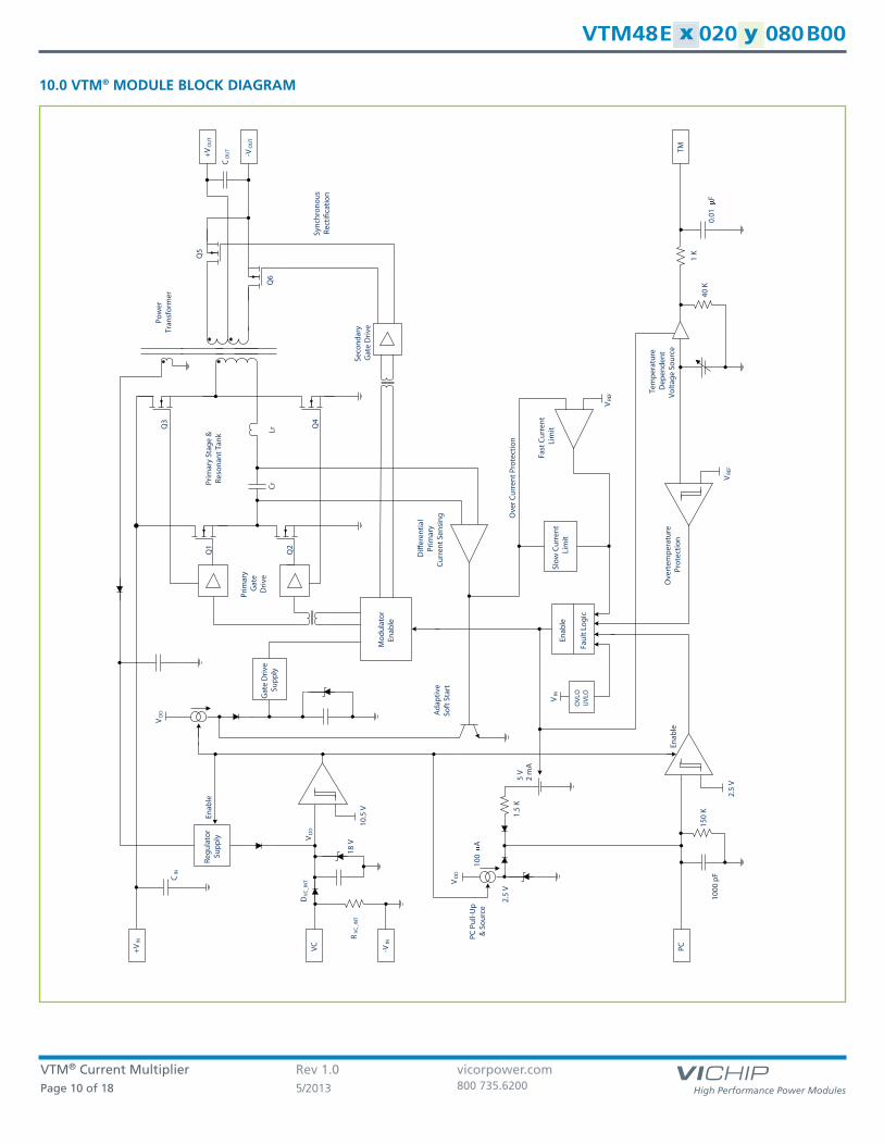
10.0 VTM® MODULE BLOCK DIAGRAM
VTM® Current Multiplier Rev 1.0 vicorpower.comPage 11 of 18 5/2013 800 735.6200
020 080 B00 yE 48 VTM x
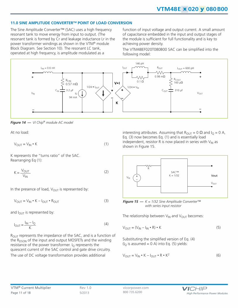
11.0 SINE AMPLITUDE CONVERTERTM POINT OF LOAD CONVERSION
The Sine Amplitude Converter™ (SAC) uses a high frequencyresonant tank to move energy from input to output. (Theresonant tank is formed by Cr and leakage inductance Lr in thepower transformer windings as shown in the VTM® moduleBlock Diagram. See Section 10). The resonant LC tank,operated at high frequency, is amplitude modulated as a
function of input voltage and output current. A small amountof capacitance embedded in the input and output stages ofthe module is sufficient for full functionality and is key toachieving power density.
The VTM48EF020T080B00 SAC can be simplified into thefollowing model:
At no load:
VOUT = VIN • K (1)
K represents the “turns ratio” of the SAC. Rearranging Eq (1):
K =VOUT (2)VIN
In the presence of load, VOUT is represented by:
VOUT = VIN • K – IOUT • ROUT (3)
and IOUT is represented by:
IOUT =IIN – IQ (4)
K
ROUT represents the impedance of the SAC, and is a function ofthe RDSON of the input and output MOSFETs and the windingresistance of the power transformer. IQ represents thequiescent current of the SAC control and gate drive circuitry.
The use of DC voltage transformation provides additional
interesting attributes. Assuming that ROUT = 0 Ω and IQ = 0 A,Eq. (3) now becomes Eq. (1) and is essentially loadindependent, resistor R is now placed in series with VIN asshown in Figure 15.
The relationship between VIN and VOUT becomes:
VOUT = (VIN – IIN • R) • K (5)
Substituting the simplified version of Eq. (4) (IQ is assumed = 0 A) into Eq. (5) yields:
VOUT = VIN • K – IOUT • R • K2 (6)
+
–
+
–
VOUT
COUTVIN
V•I
K
+
–
+
–CIN
IOUT
RCOUT
IQ
ROUT
RCIN
LIN = 5 nH
94 mA
1/24 • IOUT 1/24 • VIN
0.98 mΩRCIN 0.57 mΩ
146 pH
0.1 Ω RCOUT 160 µΩ
310 µF
LOUT = 600 pH
3.2 µFIQ
LIN = 0.6 nH IOUT ROUT
VIN VOUT
R
SACK = 1/32Vin
Vout+–
VIN
VOUT
RSAC™
K = 1/32
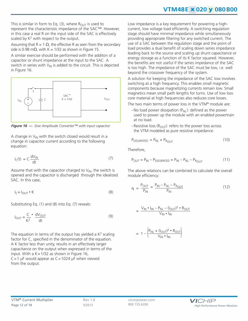
Figure 15 — K = 1/32 Sine Amplitude Converter™ with series input resistor
Figure 14 — VI Chip® module AC model
COUTCIN
VTM® Current Multiplier Rev 1.0 vicorpower.comPage 12 of 18 5/2013 800 735.6200
020 080 B00 yE 48 VTM x
This is similar in form to Eq. (3), where ROUT is used torepresent the characteristic impedance of the SAC™. However,in this case a real R on the input side of the SAC is effectivelyscaled by K2 with respect to the output.
Assuming that R = 1Ω, the effective R as seen from the secondaryside is 0.98 mΩ, with K = 1/32 as shown in Figure 15.
A similar exercise should be performed with the additon of acapacitor or shunt impedance at the input to the SAC. Aswitch in series with VIN is added to the circuit. This is depictedin Figure 16.
A change in VIN with the switch closed would result in achange in capacitor current according to the followingequation:
IC(t) = CdVIN (7)dt
Assume that with the capacitor charged to VIN, the switch isopened and the capacitor is discharged through the idealizedSAC. In this case,
IC= IOUT • K (8)
Substituting Eq. (1) and (8) into Eq. (7) reveals:
IOUT =C • dVOUT (9)K2 dt
The equation in terms of the output has yielded a K2 scalingfactor for C, specified in the denominator of the equation. A K factor less than unity, results in an effectively largercapacitance on the output when expressed in terms of theinput. With a K=1/32 as shown in Figure 16, C=1 µF would appear as C=1024 µF when viewed from the output.
Low impedance is a key requirement for powering a high-current, low voltage load efficiently. A switching regulationstage should have minimal impedance while simultaneouslyproviding appropriate filtering for any switched current. Theuse of a SAC between the regulation stage and the point ofload provides a dual benefit of scaling down series impedanceleading back to the source and scaling up shunt capacitance orenergy storage as a function of its K factor squared. However,the benefits are not useful if the series impedance of the SACis too high. The impedance of the SAC must be low, i.e. wellbeyond the crossover frequency of the system.
A solution for keeping the impedance of the SAC low involvesswitching at a high frequency. This enables small magneticcomponents because magnetizing currents remain low. Smallmagnetics mean small path lengths for turns. Use of low losscore material at high frequencies also reduces core losses.
The two main terms of power loss in the VTM® module are:
- No load power dissipation (PNL): defined as the power used to power up the module with an enabled powertrainat no load.
- Resistive loss (ROUT): refers to the power loss across the VTM modeled as pure resistive impedance.
PDISSIPATED = PNL + PROUT (10)
Therefore,
POUT = PIN – PDISSIPATED = PIN – PNL – PROUT (11)
The above relations can be combined to calculate the overallmodule efficiency:
h =POUT = PIN – PNL – PROUT (12)PIN PIN
=VIN • IIN – PNL – (IOUT)2 • ROUT
VIN • IIN
= 1 – (PNL + (IOUT)2 • ROUT)VIN • IIN
C
S
SACK = 1/32Vin
Vout+–
VINVOUTC
SAC™
K = 1/32
Figure 16 — Sine Amplitude Converter™ with input capacitor
S
VTM® Current Multiplier Rev 1.0 vicorpower.comPage 13 of 18 5/2013 800 735.6200
020 080 B00 yE 48 VTM x
12.0 INPUT AND OUTPUT FILTER DESIGN
A major advantage of a SAC system versus a conventionalPWM converter is that the former does not require largefunctional filters. The resonant LC tank, operated at extremehigh frequency, is amplitude modulated as a function of inputvoltage and output current and efficiently transfers chargethrough the isolation transformer. A small amount ofcapacitance embedded in the input and output stages of themodule is sufficient for full functionality and is key to achievinghigh power density.
This paradigm shift requires system design to carefully evaluateexternal filters in order to:
1.Guarantee low source impedance.
To take full advantage of the VTM® module dynamic response, the impedance presented to its input terminals must be low from DC to approximately 5 MHz. Input capacitance may be added to improve transient performance or compensate for high source impedance.
2.Further reduce input and /or output voltage ripple without sacrificing dynamic response.
Given the wide bandwidth of the VTM module, the source response is generally the limiting factor in the overall system response. Anomalies in the response of the source will appear at the output of the VTM module multiplied by its K factor.
3.Protect the module from overvoltage transients imposed by the system that would exceed maximum ratings and cause failures.
The VI Chip® module input/output voltage ranges must not be exceeded. An internal overvoltage lockout function prevents operation outside of the normal operating input range. Even during this condition, the powertrain is exposed to the applied voltage and power MOSFETs must withstand it.
13.0 CAPACITIVE FILTERING CONSIDERATIONS FOR A SINE AMPLITUDE CONVERTER™
It is important to consider the impact of adding input andoutput capacitance to a Sine Amplitude Converter on thesystem as a whole. Both the capacitance value and theeffective impedance of the capacitor must be considered.
A Sine Amplitude Converter has a DC ROUT value which hasalready been discussed in section 11. The AC ROUT of the SAC contains several terms:
• Resonant tank impedance
• Input lead inductance and internal capacitance
• Output lead inductance and internal capacitance
The values of these terms are shown in the behavioral model insection 11. It is important to note on which side of thetransformer these impedances appear and how they reflectacross the transformer given the K factor.
The overall AC impedance varies from model to model. Formost models it is dominated by DC ROUT value from DC tobeyond 500 KHz. The behavioral model in section 11 should beused to approximate the AC impedance of the specific model.
Any capacitors placed at the output of the VTM module reflectback to the input of the module by the square of the K factor(Eq. 9) with the impedance of the module appearing in series.It is very important to keep this in mind when using a PRM®
regulator to power the VTM module. Most PRM modules havea limit on the maximum amount of capacitance that can beapplied to the output. This capacitance includes both the PRMoutput capacitance and the VTM module output capacitancereflected back to the input. In PRM module remote senseapplications, it is important to consider the reflected value ofVTM module output capacitance when designing andcompensating the PRM module control loop.
Capacitance placed at the input of the VTM module appear tothe load reflected by the K factor with the impedance of theVTM module in series. In step-down ratios, the effectivecapacitance is increased by the K factor. The effective ESR ofthe capacitor is decreased by the square of the K factor, butthe impedance of the module appears in series. Still, in moststep-down VTM modules an electrolytic capacitor placed at theinput of the module will have a lower effective impedancecompared to an electrolytic capacitor placed at the output. Thisis important to consider when placing capacitors at the outputof the module. Even though the capacitor may be placed atthe output, the majority of the AC current will be sourced fromthe lower impedance, which in most cases will be the module.This should be studied carefully in any system design using amodule. In most cases, it should be clear that electrolyticoutput capacitors are not necessary to design a stable, well-bypassed system.

VTM® Current Multiplier Rev 1.0 vicorpower.comPage 14 of 18 5/2013 800 735.6200
020 080 B00 yE 48 VTM x
VIN VOUT
+
– DC
ZIN_EQ1
ZIN_EQ2
ZOUT_EQ1
ZOUT_EQ2
Load
VTM™1RO_1
VTM™2RO_2
VTM™nRO_n
ZOUT_EQnZIN_EQn
Figure 17 — VTM™ module array
14.0 CURRENT SHARING
The SAC topology bases its performance on efficient transferof energy through a transformer without the need of closedloop control. For this reason, the transfer characteristic can beapproximated by an ideal transformer with some resistive dropand positive temperature coefficient.
This type of characteristic is close to the impedancecharacteristic of a DC power distribution system, both inbehavior (AC dynamic) and absolute value (DC dynamic).
When connected in an array with the same K factor, the VTM®
module will inherently share the load current (typically 5%)with parallel units according to the equivalent impedancedivider that the system implements from the power source tothe point of load.
Some general recommendations to achieve matched arrayimpedances:
• Dedicate common copper planes within the PCB to deliver and return the current to the modules.
• Provide the PCB layout as symmetric as possible.
• Apply same input / output filters (if present) to each unit.
For further details see AN:016 Using BCM® Bus Converters in High Power Arrays.
15.0 FUSE SELECTION
In order to provide flexibility in configuring power systems VI Chip® products are not internally fused. Input line fusing of VI Chip products is recommended at system level to providethermal protection in case of catastrophic failure.
The fuse shall be selected by closely matching system requirements with the following characteristics:
• Current rating (usually greater than maximum current of VTM module)
• Maximum voltage rating(usually greater than the maximum possible input voltage)
• Ambient temperature
• Nominal melting I2t
16.0 REVERSE OPERATION
The VTM48EF020T080B00 is capable of reverse operation. If a voltage is present at the output which satisfies thecondition VOUT > VIN • K at the time the VC voltage is applied,or after the unit has started, then energy will be transferredfrom secondary to primary. The input to output ratio will bemaintained. The VTM48EF020T080B00 will continue tooperate in reverse as long as the input and output are withinthe specified limits. The VTM48EF020T080B00 has not beenqualified for continuous operation (>10 ms) in the reversedirection.
VTM® Current Multiplier Rev 1.0 vicorpower.comPage 15 of 18 5/2013 800 735.6200
020 080 B00 yE 48 VTM x
inchmm
NOTES:
.
DIMENSIONS ARE .2. UNLESS OTHERWISE SPECIFIED, TOLERANCES ARE:
.X / [.XX] = +/-0.25 / [.01]; .XX / [.XXX] = +/-0.13 / [.005]3. PRODUCT MARKING ON TOP SURFACE
DXF and PDF files are available on vicorpower.com4
inchmm .
DIMENSIONS ARE .2. UNLESS OTHERWISE SPECIFIED, TOLERANCES ARE:
.X / [.XX] = +/-0.25 / [.01]; .XX / [.XXX] = +/-0.13 / [.005]3. PRODUCT MARKING ON TOP SURFACE
DXF and PDF files are available on vicorpower.com
4
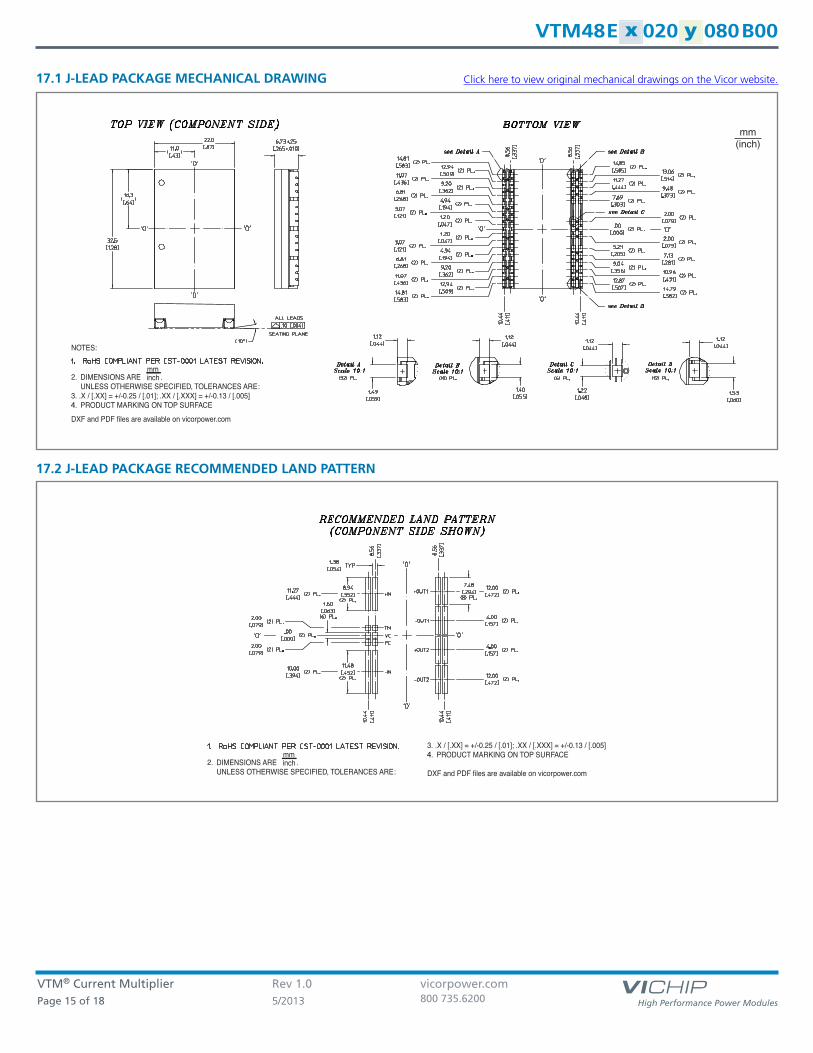
17.2 J-LEAD PACKAGE RECOMMENDED LAND PATTERN
mm(inch)
17.1 J-LEAD PACKAGE MECHANICAL DRAWING Click here to view original mechanical drawings on the Vicor website.
VTM® Current Multiplier Rev 1.0 vicorpower.comPage 16 of 18 5/2013 800 735.6200
020 080 B00 yE 48 VTM x
inchmm
NOTES:
.
DIMENSIONS ARE .2. UNLESS OTHERWISE SPECIFIED, TOLERANCES ARE:
.X / [.XX] = +/-0.25 / [.01]; .XX / [.XXX] = +/-0.13 / [.005]3. PRODUCT MARKING ON TOP SURFACE
DXF and PDF files are available on vicorpower.com4
inchmm .
DIMENSIONS ARE .2. UNLESS OTHERWISE SPECIFIED, TOLERANCES ARE:
.X / [.XX] = +/-0.25 / [.01]; .XX / [.XXX] = +/-0.13 / [.005]3. PRODUCT MARKING ON TOP SURFACE
DXF and PDF files are available on vicorpower.com
4
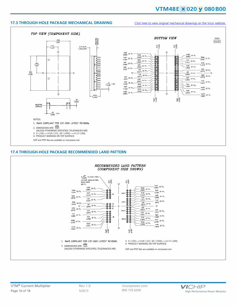
17.4 THROUGH-HOLE PACKAGE RECOMMENDED LAND PATTERN
mm(inch)
17.3 THROUGH-HOLE PACKAGE MECHANICAL DRAWING Click here to view original mechanical drawings on the Vicor website.
VTM® Current Multiplier Rev 1.0 vicorpower.comPage 17 of 18 5/2013 800 735.6200
020 080 B00 yE 48 VTM x
Notes:
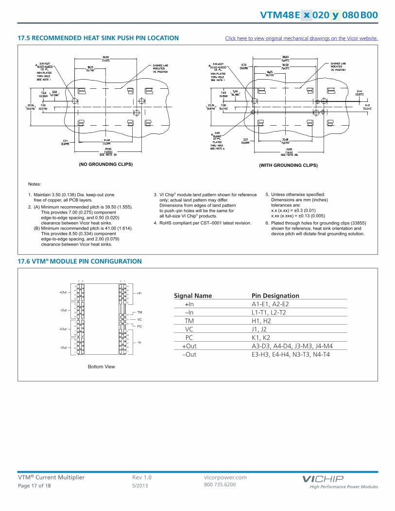
1. Maintain 3.50 (0.138) Dia. keep-out zone free of copper, all PCB layers.2. (A) Minimum recommended pitch is 39.50 (1.555). This provides 7.00 (0.275) component edge-to-edge spacing, and 0.50 (0.020) clearance between Vicor heat sinks. (B) Minimum recommended pitch is 41.00 (1.614). This provides 8.50 (0.334) component edge-to-edge spacing, and 2.00 (0.079) clearance between Vicor heat sinks.
3. VI Chip® module land pattern shown for reference only; actual land pattern may differ. Dimensions from edges of land pattern to push–pin holes will be the same for all full-size VI Chip® products.4. RoHS compliant per CST–0001 latest revision.
(NO GROUNDING CLIPS) (WITH GROUNDING CLIPS)
5. Unless otherwise specified: Dimensions are mm (inches) tolerances are: x.x (x.xx) = ±0.3 (0.01) x.xx (x.xxx) = ±0.13 (0.005)6. Plated through holes for grounding clips (33855) shown for reference, heat sink orientation and device pitch will dictate final grounding solution.
17.5 RECOMMENDED HEAT SINK PUSH PIN LOCATION
-In
PC
VC
TM
+In
-Out
+Out
-Out
+Out
Bottom View
A
B
C
D
E
F
G
H
J
K
L
M
N
P
R
T
4 3 2 1
A
B
C
D
E
H
J
K
L
M
N
P
R
T
17.6 VTM®MODULE PIN CONFIGURATION
Signal Name Pin Designation+In A1-E1, A2-E2–In L1-T1, L2-T2TM H1, H2VC J1, J2PC K1, K2
+Out A3-D3, A4-D4, J3-M3, J4-M4–Out E3-H3, E4-H4, N3-T3, N4-T4
Click here to view original mechanical drawings on the Vicor website.

VTM® Current Multiplier Rev 1.0 vicorpower.comPage 18 of 18 5/2013 800 735.6200
020 080 B00 yE 48 VTM x
Vicor’s comprehensive line of power solutions includes high density AC-DC and DC-DC modules andaccessory components, fully configurable AC-DC and DC-DC power supplies, and complete custompower systems.
Information furnished by Vicor is believed to be accurate and reliable. However, no responsibility is assumed by Vicor for its use. Vicor makes norepresentations or warranties with respect to the accuracy or completeness of the contents of this publication. Vicor reserves the right to makechanges to any products, specifications, and product descriptions at any time without notice. Information published by Vicor has been checked andis believed to be accurate at the time it was printed; however, Vicor assumes no responsibility for inaccuracies. Testing and other quality controls areused to the extent Vicor deems necessary to support Vicor’s product warranty. Except where mandated by government requirements, testing of allparameters of each product is not necessarily performed. Specifications are subject to change without notice.
Vicor’s Standard Terms and ConditionsAll sales are subject to Vicor’s Standard Terms and Conditions of Sale, which are available on Vicor’s webpage or upon request.
Product WarrantyIn Vicor’s standard terms and conditions of sale, Vicor warrants that its products are free from non-conformity to its Standard Specifications (the“Express Limited Warranty”). This warranty is extended only to the original Buyer for the period expiring two (2) years after the date of shipmentand is not transferable.UNLESS OTHERWISE EXPRESSLY STATED IN A WRITTEN SALES AGREEMENT SIGNED BY A DULY AUTHORIZED VICOR SIGNATORY, VICOR DISCLAIMSALL REPRESENTATIONS, LIABILITIES, AND WARRANTIES OF ANY KIND (WHETHER ARISING BY IMPLICATION OR BY OPERATION OF LAW) WITHRESPECT TO THE PRODUCTS, INCLUDING, WITHOUT LIMITATION, ANY WARRANTIES OR REPRESENTATIONS AS TO MERCHANTABILITY, FITNESS FORPARTICULAR PURPOSE, INFRINGEMENT OF ANY PATENT, COPYRIGHT, OR OTHER INTELLECTUAL PROPERTY RIGHT, OR ANY OTHER MATTER.
This warranty does not extend to products subjected to misuse, accident, or improper application, maintenance, or storage. Vicor shall not be liablefor collateral or consequential damage. Vicor disclaims any and all liability arising out of the application or use of any product or circuit and assumesno liability for applications assistance or buyer product design. Buyers are responsible for their products and applications using Vicor products andcomponents. Prior to using or distributing any products that include Vicor components, buyers should provide adequate design, testing andoperating safeguards.
Vicor will repair or replace defective products in accordance with its own best judgment. For service under this warranty, the buyer must contactVicor to obtain a Return Material Authorization (RMA) number and shipping instructions. Products returned without prior authorization will bereturned to the buyer. The buyer will pay all charges incurred in returning the product to the factory. Vicor will pay all reshipment charges if theproduct was defective within the terms of this warranty.
Life Support PolicyVICOR’S PRODUCTS ARE NOT AUTHORIZED FOR USE AS CRITICAL COMPONENTS IN LIFE SUPPORT DEVICES OR SYSTEMS WITHOUT THE EXPRESSPRIOR WRITTEN APPROVAL OF THE CHIEF EXECUTIVE OFFICER AND GENERAL COUNSEL OF VICOR CORPORATION. As used herein, life supportdevices or systems are devices which (a) are intended for surgical implant into the body, or (b) support or sustain life and whose failure to performwhen properly used in accordance with instructions for use provided in the labeling can be reasonably expected to result in a significant injury to theuser. A critical component is any component in a life support device or system whose failure to perform can be reasonably expected to cause thefailure of the life support device or system or to affect its safety or effectiveness. Per Vicor Terms and Conditions of Sale, the user of Vicor productsand components in life support applications assumes all risks of such use and indemnifies Vicor against all liability and damages.
Intellectual Property NoticeVicor and its subsidiaries own Intellectual Property (including issued U.S. and Foreign Patents and pending patent applications) relating to theproducts described in this data sheet. No license, whether express, implied, or arising by estoppel or otherwise, to any intellectual property rights isgranted by this document. Interested parties should contact Vicor's Intellectual Property Department.
The products described on this data sheet are protected by the following U.S. Patents Numbers:5,945,130; 6,403,009; 6,710,257; 6,911,848; 6,930,893; 6,934,166; 6,940,013; 6,969,909; 7,038,917; 7,145,186; 7,166,898; 7,187,263;7,202,646; 7,361,844; D496,906; D505,114; D506,438; D509,472; and for use under 6,975,098 and 6,984,965.
Vicor Corporation25 Frontage Road
Andover, MA, USA 01810Tel: 800-735-6200Fax: 978-475-6715
emailCustomer Service: [email protected] Support: [email protected]


![VTM-200 061733 Rev G - mcsbroadcast.commcsbroadcast.com/2012/manuals/VTM-200_061733_Rev_G[1].pdf · VTM-200 Installation and Operation Handbook OPERATOR'S SAFETY SUMMARY CAUTION —](https://img.pdfslide.us/doc/110x75/5b5e34e47f8b9a057e8bbeff/vtm-200-061733-rev-g-1pdf-vtm-200-installation-and-operation-handbook-operators.jpg)