Embed Size (px)
Citation preview
,V/qJ Ck/9-,3//,7/
S-BAND PARAMETRIC AMPLIFIER MODEL A-471(NASA-CR-139171) DEVELOPMENT AND N75-14961
FABRICATION OF S'BAND CHIP VARACTORPAPAMETRIC AMPLIFIER- Final Report, Aug.1973 - Nov. 1974 (Airborne Instruments Lab.) Unclas
182 p HC ; CSCL 09A G3/33 06932
E. H. KraemerAlL, a division of Cutler-HammerDeer Park, N.Y. 11729
November 1974
Final Report for Period August 1973 - November 1974
Prepared for:
GODDARD SPACE FLIGHT CENTERGreenbelt, Maryland 20771
NATIONAL TECHNICALINFORMATION SERVICE
US DepartMOt Of Co n rce ISpringfield, VA. 221St I
A CUTLER-HAMMERDEER PARK, LONG ISLAND, NEW YORK 11729
https://ntrs.nasa.gov/search.jsp?R=19750006889 2018-06-08T14:09:54+00:00Z
TECHNICAL REPORT STANDARD TITLE PAGE
1. Report No. 2. Government Accession No. 3. Recipient's Catalog No.
4. Title and Subtitle 5. Report DateFinal Report on Development and Fabrication of S-Band Chip November 1974Varactor Parametric Amplifier 6. Performing Organization Code
7. Author(s) 8. Performing Organization Report No.Erich Kramer
9. Performing Organization Name and Address 10. Work Unit No.
AIL, a division of Cutler-Hammer=MeJlviblG, L. I. , N. Y. 11746e-, L.I., N.Y. 11746 1. Contract or Grant No.
NAS5-20460
13. Type of Report and Period Covered
12. Sponsoring Agency Name and Address
Goddard Space Flight CenterGreenbelt, Maryland 20771Mr. Pio Dalle-Mura
14. Sponsoring Agency Code
15. Supplementary Notes
16. AbstractA noncryogenic, S-band parametric amplifier operating in the 2.2 to 2.3 GHz band and having an
average input noise temperature of less than 30 K has been built and tested. The parametric amplifier moduleoccupies a volume of less than 1-1/4 cubic feet and weighs less than 60 pounds. The module is designed foruse in various NASA ground stations to replace larger, more complex cryogenic units which require consid-erably more maintenance because of the cryogenic refrigeration system employed. The amplifier can belocated up to 15 feet from the power supply unit. Optimum performance has been achieved through the useof high-quality unpackaged (chip) varactors in the amplifier design. The attainment of these requirementsconstitutes a significant advancement in low-noise amplifier design and associated semiconductor technology.
17. Key Words 18. Distribution Statement
Parametric AmplifiersS-Band
19. Security Classif. (of this report) 20. Security Classif. (of this page) 21. No. of Pages 22. Price*Unclassified
180
* For sale by the Clearinghouse for Federal Scientific and Technical Information, Springfield, Virginia 22151.
An S-Band Parametric Amplifier achieving a 30 K input noisetemperature without use of cryogenics is described. The entire parampmodule has a volume of less than 1-1/4 cubic feet and weighs less than60 pounds. The following is a summary of the major electrical performancecharacteristics.
Frequency Range 2. 2 to 2.3 GHz
Minimum Gain 30 dB
Maximum Gain Ripple 0. 25 dB
Input Noise Temperature 28 K average
Phase Linearity ±1.5 degrees
Delay Distortion 1.4 nanoseconds maximum
Intermodulation for two -65 dBm 51 dBm downcarriers
Gain Compression (-1 dB) -46.5 dBm input
Gain Stability ±+0. 08 dB over 8 hours ,
Phase Stability +3. 5 degrees over 12 hours
The unit operates from a 115 volt ac power source with a maximurhinput power requirement of 650 watts. The details are reported herein.The unit is designed to replace some cryogenic units in various NASAearth stations.
iii
Page
I. Introduction 1-1
A. General 1-1
B. Requirements 1-2
C. Functional Description 1-6
II. Technical Discussion 2-1
A. Basic Noise Considerations in Ultra Low-Noise 2-1Noncryogenic Paramp Systems
B. Parametric Amplifier 2-5
C. Varactor 2-26
D. Circulator 2-40
E. Pump Source 2-50
F. Environmental Considerations 2-54
G. Packaging Requirements 2-63
H. Reliability Prediction 2-66
III. Measured Performance 3-1
A. General 3-1
B. Breadboard System 3-1
C. Measured Performance - Prototype System 3-3
IV. New Technology Developments 4-1
V. Conclusions and Recommendations 5-1
A. Conclusions 5-1
B. Recommendations 5-1
VI. References 6-1
* v
Page
VII. Appendixes 7-1
A. Computer Model of Parametric Amplifier Circuit A-1
B. Gain Changes as a Function of Circulator Isola- B-1tion Changes
C. Noise Transfer Analysis--Single Stage Para- C-1metric Amplifier
D. Test Procedure for Evaluation of Nonhermetically D-1Sealed Gallium Arsenide Varactor
E. Summary of Diode Evaluation Data E-1
F. Noise Transfer Analysis--General Case for F-1Multistage Parametric Amplifier System
vi
Figure Page
1-1 Specified Mechanical Outline of Paramp Enclosure 1-4
1-2 Simplified Functional Block Diagram of S-Band System 1-7
1-3 Remote Control/Power Supply Unit Block Diagram 1-8
1-4 Paramp Module and Remote Control/Power Supply Unit 1-11Comprising A471 System
2-1 Simple Equivalent Circuit for Calculating Noise 2-4
2-2 Joise Degradation Versus Antenna Return Loss 2-7
2-3 Final System Gain/Noise Temperature Budget 2-8
2-4 Schematic Diagram of Balanced Parametric Amplifier 2-9With Propagating Idler
2-5 Varactors in Waveguide 2-9
2-6 Parametric Amplifier Configuration 2-11
2-7 Block Diagram of Broadband Parametric Amplifier 2-11Theoretical Model
2-8 Noise Temperature as a Function of Pump Frequency 2-16and M
2-9 Theoretical Single Stage Gain for Proposed Balanced 2-16Parametric Amplifier With Ideal Circulator
2-10 Parametric Amplifier Mount 2-19
2-11 Least Squares Error Fit of Theoretical Paramp Phase 2-24Characteristic to Third-Order Polynomial
2-12 Varactor Holder 2-27
2-13 Assembled Quanar Varactor 2-28
2-14 Typical Varactor I Versus V Trace 2-29
2-15 Varactor C Versus V 2-30
vii
Figure Page
2-16 Impedance Plot of M-S Junction 2-32
2-17 Equivalent Circuit of Chip Varactor and Holder 2-33
2-18 Effect of Temperature on Varactor Contact 2-35
2-19 Various Circulator Paramp Configurations 2-41
2-20 Circulator Representation at T = T and T = T + AT 2-44o O
2-21 Magnetization as Function of dc Field and Ms 2-46
2-22 Degradation of Tangential Sensitivity as a Function of 2-52Absolute Power of Interfering Signal
2-23 Typical Bipolar Temperature Controllers 2-55
2-24 Paramp Module, Site Interface Outline 2-56
2-25 Paramp Module 2-60
2-26 First-Stage Circulator-Paramp Assembled to Thermo- 2-61electric Chill Plate and Input Transition
2-27 Lower Compartment Components Drawer (Partially 2-65Wired)
2-28 Remote Control/Power Supply Chassis 2-67
3-1 Measured Breadboard Room Temperature Performance 3-6
3-2 Measured Breadboard System Saturation Characteristics 3-7
3-3 Prototype Components for S-Band Chip Varactor 3-8System - Breadboard Tests
3-4 Gain-Bandwidth Characteristics 3-9
3-5 Noise Temperature Versus Frequency 3-10
3-6 Input-Output VSWR Versus Frequency 3-11
3-7 Dynamic Range Versus Frequency 3-12
3-8 Phase Linearity Versus Frequency 3-13
3-9 Envelope Delay Distortion Versus Frequency 3-14
3-10 Gain Stability Under Thermal Cycling 3-15
5-1 Comparison of the Prototype System With a Typical 5-2Equivalent Cryogenic Unit
viii
Figure Page
5-2 Proposed Production Model - LNA Configuration 5-5
5-3 Proposed Production Model - Front View 5-7
5-4 Proposed Production Model - Lower Compartment 5-9
ix,
A. GENERAL
This report describes an S-band Parametric Amplifier System (AILModel A-471) that has achieved a 30 K effective input noise temperature with-out using cryogenic refrigerators. The entire paramp unit has a volumeof less than 1-1/4 cubic feet and is designed to meet the site interfacerequirements of various NASA ground stations. The remote power supplyunit fits in a standard 19-inch rack and occupies only 7 inches of rackspace. The amplifier is capable of operating over long periods of timewith minimum maintenance. Since production versions of this prototype willeventually be required, the unit has been engineered so that only a minimumof engineering effort will be needed to evolve a production design of highreliability.
A number of approaches were considered in an effort to determine theoptimum configuration that could be used for the paramp system that wouldmeet the required specifications. The overall size limitations normally as-sociated with a system when mounted in operational antenna structures, thethermal and vibration environment encountered, and the desirability for ahigh degree of long-term stability, power requirements, and the humanengineering factors associated with operating and maintaining the systemhave been assessed. With these design criteria and constraints taken intoaccount, the following approach was formulated for the ultra low-noise non-cryogenic S-band paramp system.
The approach evolved for this program is both simple and practicaland has a high probability of success. The system consists of two identicalstages of parametric amplification, each stage consisting of a single-endedparametric amplifier employing the proven AIL passivated quasiplanar(QUANAR) chip-type varactor coupled to a four-port circulator. The pumpsource consists of a separate 50-GHz fundamental Gunn oscillator for eachstage. The first stage parametric amplifier and circulator are temperature-stabilized at -20 0 C using thermoelectric modules, while the remainder ofthe enclosure is stabilized at a temperature of +50 0 C.
The unit exceeds the following original electrical performance require-ments with the exception of gain stability versus ambient temperature whichdeviates slightly more than (1 dB) from the design goal specification (below100C).
1-1
B. REQUIREMENTS
NASA Contract NAS-5-20460 defines the following requirements for
the S-band paramp system:
* Two-stage paramp system, all solid state in design,packaged in a temperature controlled enclosure whichincludes all necessary power supplies
* Center frequency 2250 ±10 MHz
S Bandwidth (-1 dB point) 100 to 150 MHz
* Midband gain 30 dB (minimum)
* Noise temperature 30 K (maximum) from2210 to 2290 MHz
35 K (maximum) from2200 to 2300 MHz
* Gain ripple 0.5 dB peak-to-peak (maximum)over band pass, except 1.0 dBpeak-to-peak (maximum) at bandedges
* Gain compression -50 dBm (minimum) (referred to
(1-dB point) input)
S Input/output VSWR 1.5:1 (maximum) with amplifieroperating at full gain conditionsand terminated with a load havinga return loss of 10 dB or greater
* Phase linearity t2 degrees from 2215 to 2285 MHzt 5 degrees from 2200 to 2215 MHz± 5 degrees from 2285 to 2300 MHz
* Phase slope 0. 5 degree/MHz (maximum)(deviation from linearity) from 2200 to 2300 MHz
* Envelope delay distortion 5 ns (maximum) from 2200 to2300 MHz
* Delay slope 1 ns/MHz (maximum) from2200 to 2300 MHz
* Phase stability 5 degrees over a 12 hour period
* Gain stability ±0.5 dB over an 8 hour periodat an ambient temperature of60 to 80 0 F
1-2
0 Ambient temperature range -15 0 C to +50 0 C
* Gain stability over ambient ±+1 dB (maximum)temperature range
0 Spurious response -100 dBm (maximum) at fp-125 dBm (maximum) at otherfrequencies
0 Intermodulation products At least 50 dB below the outputof two carriers with equal inputpowers of -65 dBm
* Primary power 117 volts ac ± 10 percent,58 to 62 Hz
S Reliability The paramp system shall exhibitan MTBF of 16, 000 hours
* Humidity 10 to 95 percent
* Orientation Any
* Vibration and shock The paramp system shall operatewithin specification when sub-jected to vibration and shocknormally encountered in an an-tenna system employing a hydraulicdrive.
A change in scope after the breadboard phase added the followingrequirements.
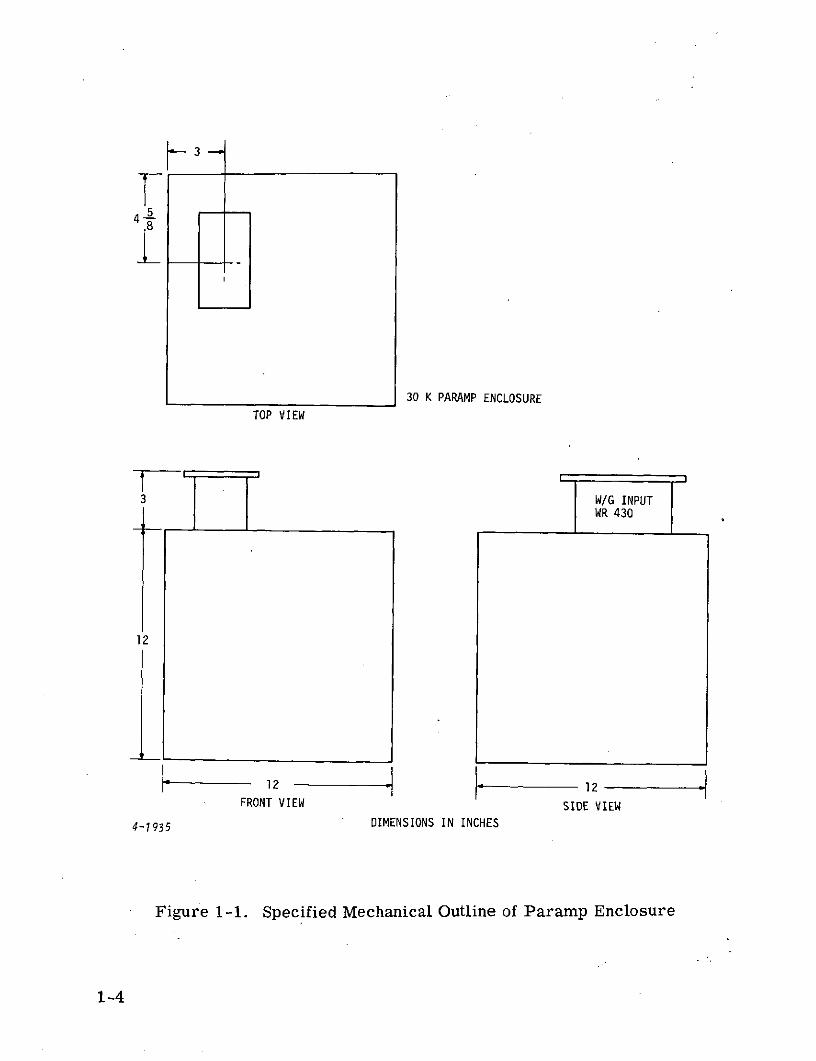
S Figure 1-1 indicates the maximum dimensions permis-sible for the proposed paramp. In addition to the stateddimensions, the enclosure shall have no protrusions onthe sides except for mounting lugs. The unit will bemounted with the back adjacent to a bulkhead surface.Interior access for normal maintenance shall be fromthe front. All connections and controls will be locatedon the front or top surface. They shall be positionedin such a manner that they will not interfere with otherequipment when installed in the system nor shall theyinterfere with the ability to perform normal maintenanceon the paramp.
S The paramp will be installed as a dual system in twoconfigurations. The 28-meter antenna installationrequires close dimensional tolerances on the parampto be physically integrated into the antenna system.This dictates tight design requirements for the me-chanical configuration.
1-3
3-
45
4-8
30 K PARAMP ENCLOSURE
TOP VIEW
3 -'W/G INPUT3WR 430
12
S12 12FRONT VIEW SIDE VIEW
4-1935 DIMENSIONS IN INCHES
Figure 1-1. Specified Mechanical Outline of Paramp Enclosure
1-4
These requirements have been reviewed in detail. The significantareas of design and development that were essential to the successful com-pletion of the program were as follows.
1. VARACTOR
In order to obtain the specified operational levels (primarily noiseperformance), a varactor of superior quality was required. Standard com-mercial packaged varactors provide performance that falls far short ofthe minimum program requirements. The NASA work statement explicitlynoted this in advising the use of a chip varactor.
2. PARAMP/CIRCULATOR
Assuming the availability of a superior varactor, it was essential tominimize all signal circuit losses (including circulator input loss) in thefirst-stage paramp in order to meet the required noise performance. Idlercircuit losses were minimized and varactor current flow at the sum frequencysideband was controlled to prevent the transfer of a positive resistancecomponent from the idler to the signal circuit. Neglect of these importantfactors would have resulted in degraded noise performance.
3. PUMP SOURCE
In addition to the previously listed requirements, it was essential toprovide a millimeter-wave pump source to obtain the noise performancespecified. Additionally, the pump source was all solid state for prolongedlife and high reliability.
4. PHYSICAL REQUIREMENTS
System components have been selected to provide a high degree oflong-term stability. The temperature-controlled enclosure was designedto provide the required gain stability of ± 1 dB over the ambient temperaturerange of -15 0 C to +50 0 C for a continuous period of 30 days.
5. QUALITY ASSURANCE AND RELIABILITY REQUIREMENTS
Quality Assurance and Reliability groups were involved in all phasesof this program from design, procurement, and assembly to acceptancetesting.
1-5
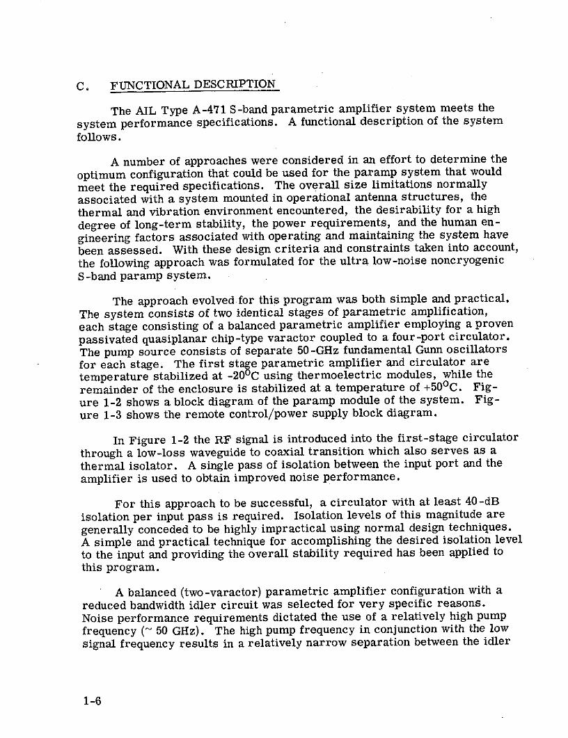
C. FUNCTIONAL DESCRIPTION
The AIL Type A-471 S-band parametric amplifier system meets the
system performance specifications. A functional description of the systemfollows.
A number of approaches were considered in an effort to determine the
optimum configuration that could be used for the paramp system that would
meet the required specifications. The overall size limitations normallyassociated with a system mounted in operational antenna structures, the
thermal and vibration environment encountered, the desirability for a high
degree of long-term stability, the power requirements, and the human en-
gineering factors associated with operating and maintaining the system have
been assessed. With these design criteria and constraints taken into account,the following approach was formulated for the ultra low-noise noncryogenicS-band paramp system.
The approach evolved for this program was both simple and practical.
The system consists of two identical stages of parametric amplification,each stage consisting of a balanced parametric amplifier employing a proven
passivated quasiplanar chip-type varactor coupled to a four-port circulator.
The pump source consists of separate 50-GHz fundamental Gunn oscillatorsfor each stage. The first stage parametric amplifier and circulator are
temperature stabilized at -20 0 C using thermoelectric modules, while the
remainder of the enclosure is stabilized at a temperature of +50 0 C. Fig-
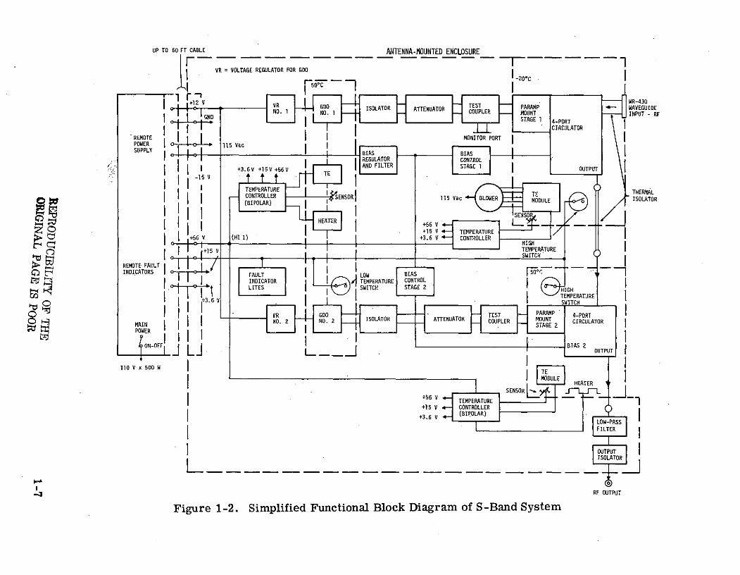
ure 1-2 shows a block diagram of the paramp module of the system. Fig-
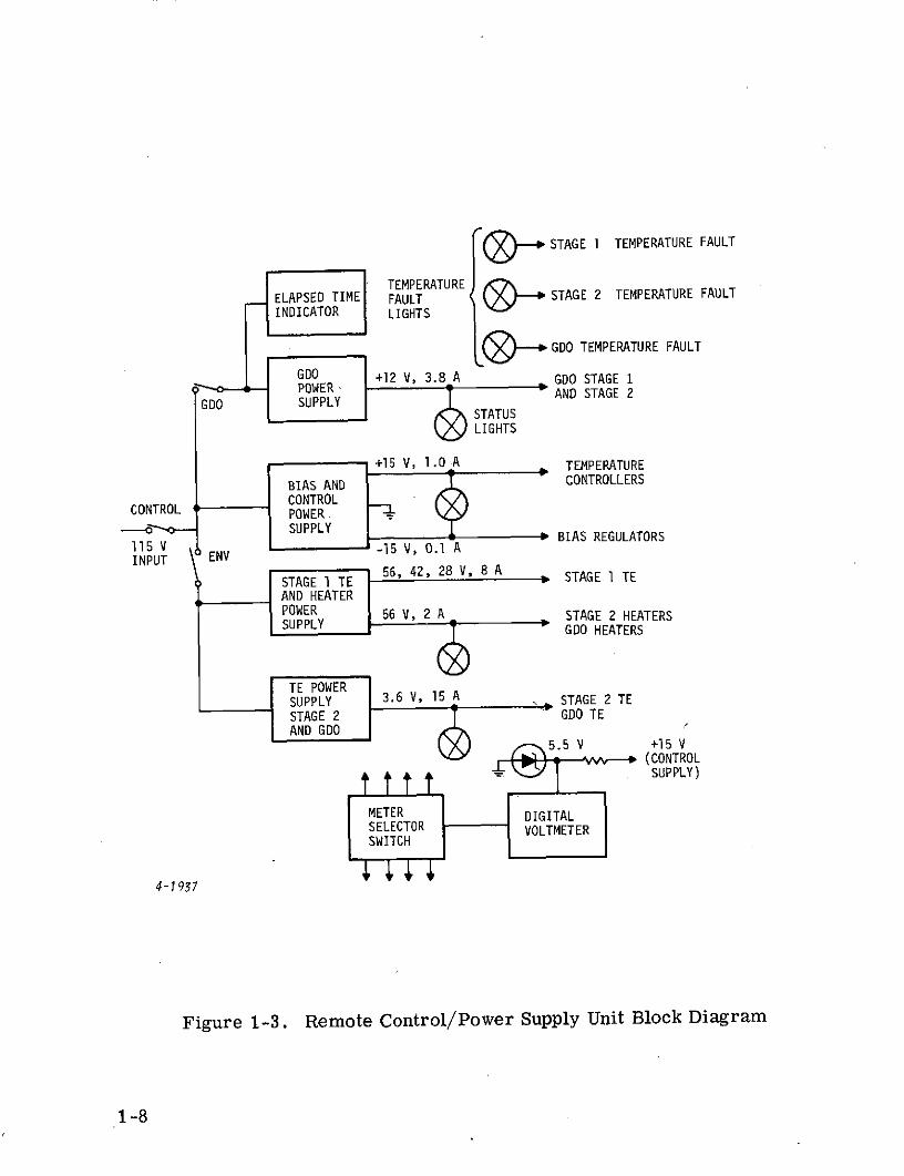
ure 1-3 shows the remote control/power supply block diagram.
In Figure 1-2 the RF signal is introduced into the first-stage circulator
through a low-loss waveguide to coaxial transition which also serves as a
thermal isolator. A single pass of isolation between the input port and the
amplifier is used to obtain improved noise performance.
For this approach to be successful, a circulator with at least 40-dB
isolation per input pass is required. Isolation levels of this magnitude are
generally conceded to be highly impractical using normal design techniques.A simple and practical technique for accomplishing the desired isolation levelto the input and providing the overall stability required has been applied tothis program.
A balanced (two-varactor) parametric amplifier configuration with a
reduced bandwidth idler circuit was selected for very specific reasons.
Noise performance requirements dictated the use of a relatively high pumpfrequency (- 50 GHz). The high pump frequency in conjunction with the low
signal frequency results in a relatively narrow separation between the idler
1-6
UP TO 60 FT CABLE ANTENNA-MOUNTED ENCLOSURE
VR = VOLTAGE REGULATOR FOR GDO I
r- Fc--20*C
,+12 V WR-430GDO L A TEST PARAMP - WAVEGUIDE
D ISOLATOR ATTENUATOR MOUNT INPUT - RFSTAGE 1 4-PORT
REMOTE MONITOR PORTPOWER 115 VacSUPPLY c I I IFAS BIAS
REGULATOR CONTROL
+3.6V +15V +56V AND FILTERSTAGE I OUTPUT
-1 15 V NSORTA 1 : VOcUULEUTO
' I IIi I - t -- I+TEMPERATURE ', THEL
CONTROLLER IENSOR TE VTCOETRo(BIPOLAR) 115 Vac BLOWER MODULE ISOLATOR
+15 V TEMPERATURE1+ ' 6 HI1 +.6 V -CONTROLLER I
cI I TEMPERATURE
REMOTE FAULT SWITCH
INDICATORS FAULTA II I1I
INIATRTEMPERATURE CONTROLI- WLITE ITCH STAGE 2 NIGH.- IITEMPERATURE II SW
IT CH
R NOE . 2 ISOLATOR ATTENUATOR COUPLER -IRCATOR
TESTPARAMP " 4-POR IMAIN liiRULTO IPOWER
ON-OFF BLAS 2I- J _ OUTPUT110 V1x 500 W te
IMODULESENSORLow HEATER I+56 V TEMPERATURE
+15 V CONTROLLER
+ 3 .6 V ( B I P O L A R ) L O :-P A S S
OUTPUT
ISOLATORI
I RF OUTPUT
Figure 1-2. Simplified Functional Block Diagram of S-Band System
O--r STAGE 1 TEMPERATURE FAULT
TEMPERATUREELAPSED TIME FAULT STAGE 2 TEMPERATURE FAULT
INDICATOR LIGHTS
---D GDO TEMPERATURE FAULT
GDO +12 V, 3.8 A GDO STAGE 1
SPOWER AND STAGE 2
LIGHTS
+15 V, 1.0 A TEMPERATURE
BIAS AND CONTROLLERSCNTRCONTROL
POWER 56 V, 2 ASUPPLY
115- V BIAS REGULATORSI5 V E -15 V, 0.1 A
STAGE 1 TE 56, 42, 28 V, 8 A p STAGE 1 TEAND HEATERPOWER 56 V, 2 A STAGE 2 HEATERSSUPPLY - GDO HEATERS
TE POWERSUPPLY 3.6 V, 15 A STAGE 2 TESTAGE 2 GDO TEAND GDO
(CONTROLSUPPLY)
METER DIGITALSELECTOR VOLTMETERSWITCH
4-1937
Figure 1-3. Remote Control/Power Supply Unit Block Diagram
1-8
(difference-frequenoy) sideband and the sum-frequency sideband. Varactorcurrent flow at the sum-frequency sideband is detrimental and results indegraded noise and gain-bandwidth performance. For this reason, the idlercircuit bandwidth has been controlled and cannot be arbitrarily widened.The balanced amplifier configuration is capable of a wider idler bandwidththan a single-ended design, resulting in greater inherent stability, sinceless double-tuning is required to achieve the required gain bandwidth product.
Since the signal frequency .is relatively low, large-diameter coaxiallines were used for signal-circuit tuning and to achieve the required signal-circuit impedance transformations. The propagation of higher-order modesin the coaxial lines, which presents problems in the signal circuit design ofhigher signal frequency paramps such as Ku-band, is not a problem at S-band.
The large-diameter lines which were used minimize signal circuit losses andresult in a high effective varactor quality factor (Mef f) in the signal circuit.
A fundamental Gunn oscillator at a frequency of - 50 GHz was chosenfor the pump source. The Gunn device was chosen primarily because ofnoise considerations; suitable Gunn oscillators with the required power out-put level are available commercially at the present time. The millimeterwave pump circuit is simple and reliable, since a frequency multiplier isnot required. Elaborate stabilization schemes which would be required foran avalanche device are not necessary with a Gunn oscillator.
The choice of a separate pump source for each stage was a judiciousone. This type of operation eliminates interfering signals coupling fromone stage to the other which can happen when a single souce is utilized. Inaddition, for the same stability attained for the source, the overall gainand phase stability of the system is improved over that of a- common sourcesince changes add on an rms basis rather than on a linear basis.
The two stages are coupled with a dc block, which provides the re-quired dc bias isolation between stages. The output of the system also con-tains a dc block and isolator, as well as a low-pass filter to ensure com-pliance with the spurious output requirement by providing rejection at thepump and idler frequencies.
The thermoelectric modules used to stabilize the first stage paramp/circulator at a temperature of -20 0 C also provide an enhancement in noisetemperature for this stage. It is theoretically possible to stabilize the firststage at a somewhat higher temperature and meet the noise performancerequirement by pumping at a higher frequency. This would, however,introduce serious problems in providing low loss separation of the idler andpump frequencies, as well as aggravate the sum frequency problem. To
1-9
obtain sufficient pump power at a higher pump frequency with sufficient
spectral purity, it would be necessary to resort to a Gunn oscillator followed
by a varactor multiplier (doubler). Besides complicating the pump network,this approach would be more complex.
A remote control is provided on the power supply unit for both control
and monitoring system performance. It contains the system on/off switch
and standby/operate switches. Tuning controls on the paramp module con-
sist of a bias voltage adjustment (10-turn pot) and a mechanical adjustment
of the pump power attenuator for each stage, as well as a vernier control
of the GDO voltage. A digital meter is provided on the remote control/
power supply unit for checking the following:
* Paramp bias voltage of each stage
* Gunn oscillator voltage of each stage
* Gunn and thermal stabilization power supply voltages
* Thermal fault indicator voltages
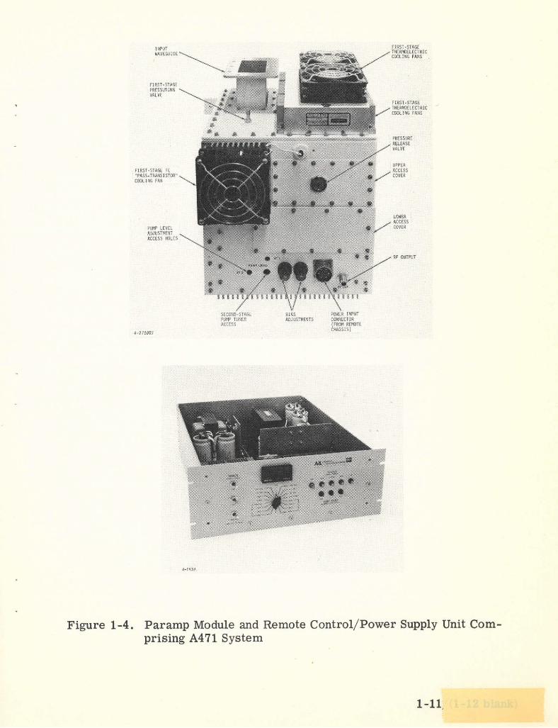
The design concept that was utilized for this program is a modular
approach. This enables simple, rapid, and efficient fault location as well
as repair of the equipment, if required. Figure 1-4 shows the parampmodule (with second stage control access cover removed). Also shown in
this figure is the remote control and power supply unit.
1-10
INPUT FIRST-STAGEWAVEGUIDE THERMOELECTRICWAVEGUIDE COOLING PANS
FIRST-STAGEPRESSURINSVALVE
FIRST-STAGETRETOLECTRIC
RELEASESVALVE
UPPERFIRST-STAGE TE ' ACCESS
PASS-TRANSISTOR" 4 COVERCOOLING FAN
LOWERACCESS
PUMP LEVEL a -','-" COVERADJUSTMENTACCESS HOLES
r RF OUTPUT
/\
SECOND-STAsE BIAS POWER INPUTPUMP TUNER ADJUSTMENTS CONNECTORACCESS (FROM REMOTE
4-2,720RI CHASSIS)
4-1934
Figure 1-4. Paramp Module and Remote Control/Power Supply Unit Com-prising A471 System
1-11.
A. BASIC NOISE CONSIDERATIONS IN ULTRA LOW-NOISE NON-CRYOGENIC PARAMP SYSTEMS
Theoretically, paramps at lower microwave signal frequencies havingmillimeter-wave pumps can exhibit ultra low-noise temperature even whenoperated at or near room temperature because of the high idler-to-signalfrequency ratio. Practically, however, at least three interdependent sourcesof noise temperature degradation must be considered before these ultra lowvalues can be realized. These effects are:
* System input losses
* Sum frequency noise
* Antenna mismatch noise degradation
Two of these effects are direct functions of the physical temperature,which is why they are particularly important in a noncryogenic amplifier.Each of these considerations is discussed in detail in the following para-graphs.
1. SYSTEM INPUT LOSSES
Input circuit losses between the antenna port and the pumped varactoror varactors of the first stage paramp directly degrade the noise tempera-ture in accordance with the relation:
AT =(L - 1) (T L + Tamp) (2-1)
where
L = total loss
TL = physical temperature of losses
T = noise temperature of amplifier in the absence of lossesamp
2-1
As an example, some typical values of L = 0.2 dB, T L = 300 K, and
T = 15 K yield AT = 14. 8 K. The principal source of this loss is forwardamp
loss of the usual input circulator. Minimization of this loss was accom-plished by the use of only one pass ahead of the amplifier as discussed inparagraph D. A possible alternative design, namely the use of a pair ofidentical amplifiers connected to a 90-degree hybrid coupler, while havingthe advantage of lower losses, would be severely degraded by antenna mis-match (paragraph A. 3) and this approach was therefore ruled out early in theprogram.
2. SUM FREQUENCY NOISE
The simple noise temperature formula to be presented in paragraph Bassumes that the varactor or varactors see an open circuit at the sum fre-quency, f = f + f . Qualitatively, this is a good assumption only as long
sum p sas fsum - fi = 2fs (BW)i/2, where (BW)i equals the idler circuit 3-dB band-
width. For high values of idler to signal frequency ratios, such as wereconsidered for this program, this condition can easily be violated. Theresult is that Johnson noise in the sum frequency band originating from thevaractor series resistance is converted by the pump back to the signal bandand can seriously degrade the noise temperature. A complicated analysisof this effect is included in Appendix A, but a simple approximation isgiven by the relation:
AT fi0 (BW)iT f i (2-2)
T 4Q. f 4famp i sO sO
where Qi is the idler circuit Q. As an example, some values typical of a
balanced high idler paramp designed for maximum gain-bandwidth product,namely, Qi = 10, fi0 = 50 GHz, fs0 = 2.25 GHz, and Tamp = 15 K yield
AT 5.6 K.
The obvious cure for this sum frequency noise degradation is to narrowthe idler bandwidth. Then, however, to achieve the desired overall bandwidthperformance, the amount of multiple (double) tuning compensation in the sig-nal circuit must be increased. This results in increased signal circuit losswith consequent noise temperature degradation (paragraph A. 1).
2-2
3. ANTENNA MISMATCH NOISE DEGRADATION
Ordinarily, amplifier noise temperature is specified using a theoreti-cally perfectly matched antenna. Practically, however, some antenna mis-match must be expected, and, if the amplifier noise temperature is severelydegraded by a relatively small antenna mismatch, the effect should be con-sidered by the system designer. Figure 2-1 is a simple representation of howthis degradation arises in the usual circulator-coupled parametric amplifier
for the case of either one or two passes ahead of the amplifier.
Referring to the figure, for either case (A) or (B) and assuming idealcirculators, noise power from the termination R0 at physical temperature
TL is directly transmitted to the antenna port where it encounters reflection
coefficient F ant. The resultant reflected noise power then enters the normal
signal channel to degrade the noise temperature. The magnitude of this effectcan be calculated as follows. The additional noise power referred to the am-
2plifier input terminals is proportional to I r ant I2 L' while the signal channelsuffers a loss in gain by the factor (1 - I and 12). Thus the noise tempera-
andture degradation is:
AT -r f antl T L + T amp_ T
1 - ant2 ampant
(2-3)
Sant +T
1- ant 2 L amp]
As an example, using the typical numbers i ant 2 = 0.04 (corresponding to
a VSWR of 1.5), TL = 300 K, and Tam p -= 15 K yields A.T = 13.1 K. Addi-
tionally, if the passive circulator match at the antenna port is not perfect, itcan phase with the antenna mismatch to give an effective larger value ofIran t
2-3
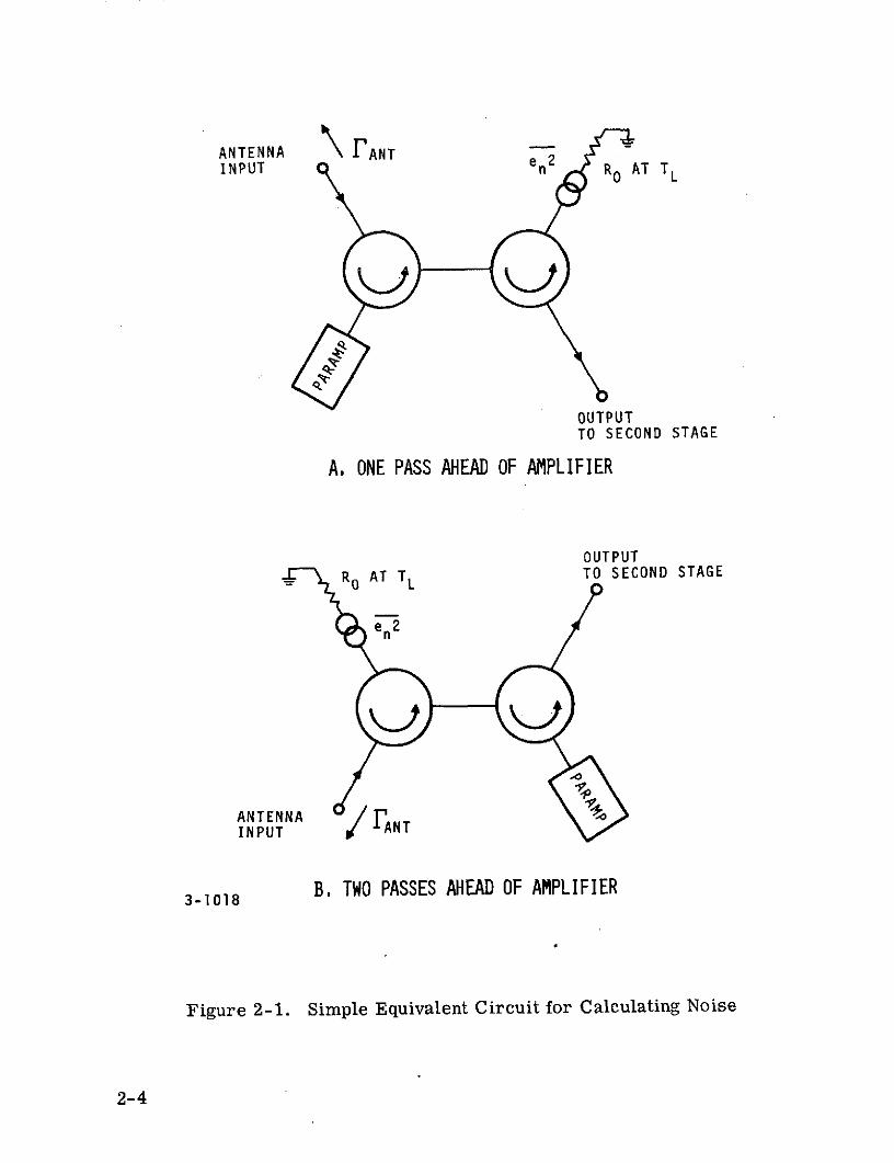
ANTENNA \7N eAT
INPUTn R AT T
OUTPUTTO SECOND STAGE
A. ONE PASS AHEAD OF AMPLIFIER
OUTPUT
ROAT TL TO SECOND STAGE
e n2
ANTENNA ANTINPUT -A
3-1018 B. TWO PASSES AHEAD OF AMPLIFIER
Figure 2-1. Simple Equivalent Circuit for Calculating Noise
2-4
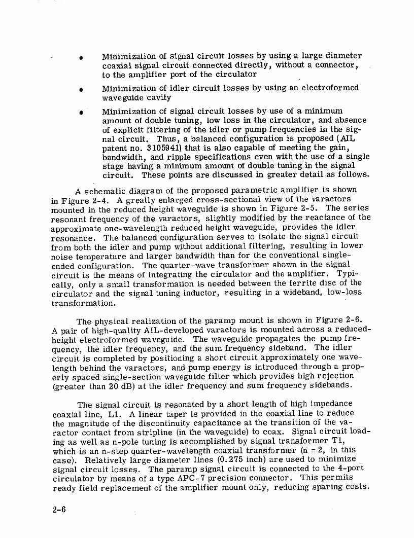
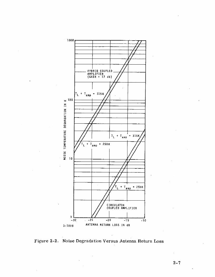
Figure 2-2 shows the noise temperature as a function of antenna returnloss according to equation 2-3 for two values of TL + Tamp = 258 and 315 K.
LampFigure 2-3 shows the system gain/noise budget. Also shown for comparisonare the corresponding values for a hybrid-coupled amplifier with 17-dB gain.This figure clearly shows the extreme sensitivity of the hybrid-coupledamplifier to antenna mismatch. For this reason, only the circulator-coupled amplifier was considered.
B. PARAMETRIC AMPLIFIER
1. GENERAL
The key of the paramp design is the required overall maximum noisetemperature specification of 30 K over most of the band from 2200 to2300 MHz for an ambient temperature of up to +50 0 C. To attain this value,both single-ended and balanced parametric amplifier configurations wereinvestigated. The single-ended approach has an inherently narrower band-width idler circuit, and a theoretical analysis indicated that it would give aslightly lower (16 K versus 18 K) noise temperature. A single-ended mountwas built, and experimental evaluations indicated that the idler loading dueto finite decoupling of the signal circuit chokes reduced the effective idlerfigure of merit. This actually would cause greater degradation in noiseperformance then the reduction in sum-frequency current occasioned bythe narrower bandwidth idler circuit. In addition, the greater degree ofdouble tuning required would also degrade the signal circuit figure of merit,which would again degrade the noise performance. The only solution to theproblem would be a dual set of signal circuit chokes. These would, however,produce more narrowbanding in the signal circuit.
During this period, a balanced mount was successfully developed asan alternate approach. Further pursuit of the single-ended approach wastherefore halted, and the remainder of the effort concentrated on the bal-anced mount.
The following other amplifier parameters and circuit configurationswere used:
* Pump frequency of about 50 GHz which is the highest frequencycommercially available fundamental low-noise Gunn oscillatorsource
* A four-port special low-loss circulator
* A balanced high idler mount with a tuning short located onewavelength from the varactors to minimize sum frequencynoise by using a relatively narrowband idler circuit with highcutoff-frequency chip varactors
2-5
* Minimization of signal circuit losses by using a large diametercoaxial signal circuit connected directly, without a connector,to the amplifier port of the circulator
* Minimization of idler circuit losses by using an electroformedwaveguide cavity
* Minimization of signal circuit losses by use of a minimumamount of double tuning, low loss in the circulator, and absenceof explicit filtering of the idler or pump frequencies in the sig-nal circuit. Thus, a balanced configuration is proposed (AILpatent no. 3105941) that is also capable of meeting the gain,bandwidth, and ripple specifications even with the use of a singlestage having a minimum amount of double tuning in the signalcircuit. These points are discussed in greater detail as follows.
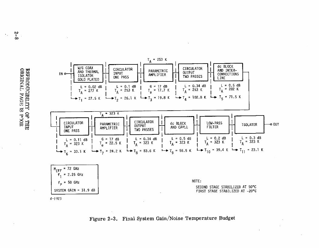
A schematic diagram of the proposed parametric amplifier is shown
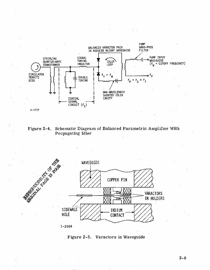
in Figure 2-4. A greatly enlarged cross-sectional view of the varactorsmounted in the reduced height waveguide is shown in Figure 2-5. The series
resonant frequency of the varactors, slightly modified by the reactance of the
approximate one-wavelength reduced height waveguide, provides the idler
resonance. The balanced configuration serves to isolate the signal circuitfrom both the idler and pump without additional filtering, resulting in lower
noise temperature and larger bandwidth than for the conventional single-ended configuration. The quarter-wave transformer shown in the signalcircuit is the means of integrating the circulator and the amplifier. Typi-cally, only a small transformation is needed between the ferrite disc of the
circulator and the signal tuning inductor, resulting in a wideband, low-losstransformation.
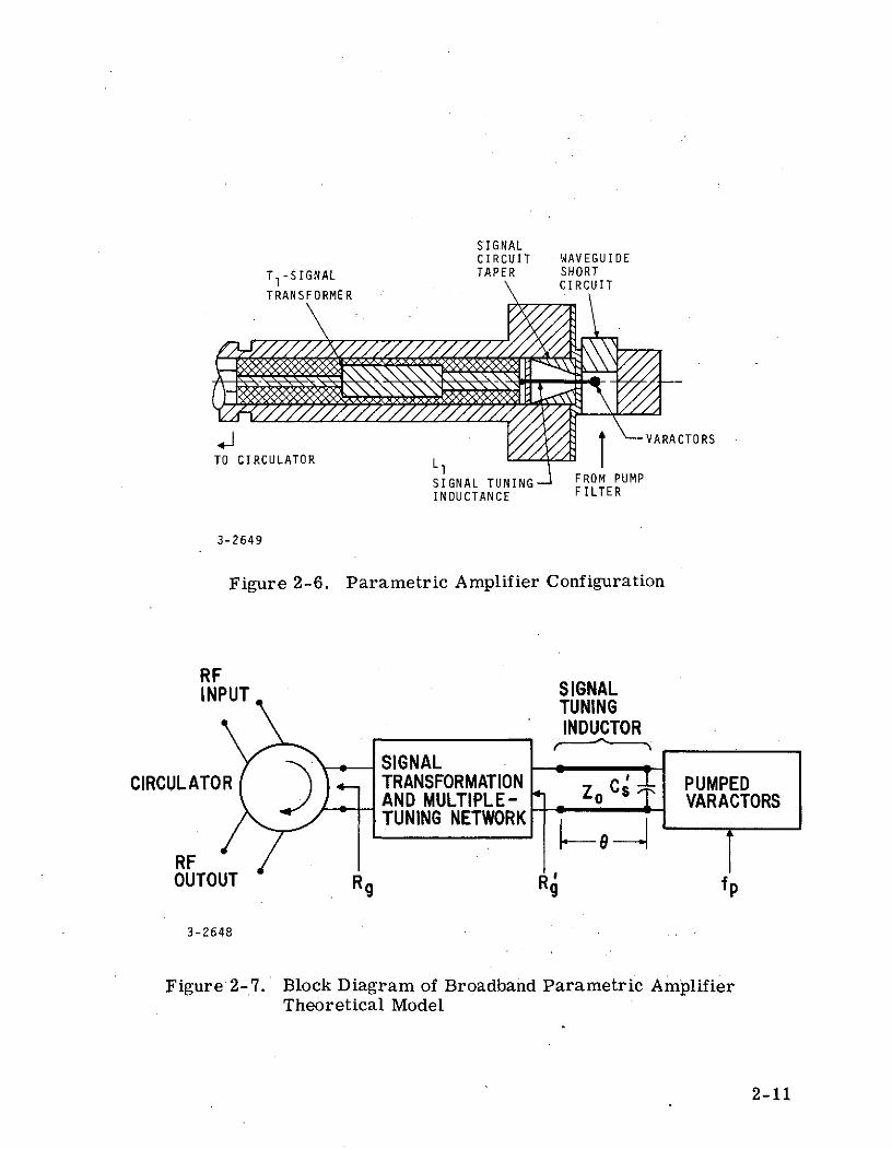
The physical realization of the paramp mount is shown in Figure 2-6.
A pair of high-quality AIL-developed varactors is mounted across a reduced-height electroformed waveguide. The waveguide propagates the pump fre-quency, the idler frequency, and the sum frequency sideband. The idler
circuit is completed by positioning a short circuit approximately one wave-
length behind the varactors, and pump energy is introduced through a prop-
erly spaced single-section waveguide filter which provides high rejection
(greater than 20 dB) at the idler frequency and sum frequency sidebands.
The signal circuit is resonated by a short length of high impedance
coaxial line, L1. A linear taper is provided in the coaxial line to reducethe magnitude of the discontinuity capacitance at the transition of the va-ractor contact from stripline (in the waveguide) to coax. Signal circuit load-
ing as well.as n-pole tuning is accomplished by signal transformer T1,which is an n-step quarter-wavelength coaxial transformer (n = 2, in thiscase). Relatively large diameter lines (0. 275 inch) are used to minimizesignal circuit losses. The paramp signal circuit is connected to the 4-portcirculator by means of a type APC-7 precision connector. This permitsready field replacement of the amplifier mount only, reducing sparing costs.
2-6
1000
HYBRID COUPLEDAMPLIFIER(GAIN = 17 dB)
TL + Tamp =315
100
I-
L
TL + Tamp = 315KL amp
La
TL +Tam p =258K
S10
/ T + T = 258K
ampm
CIRCULATORCOUPLED AMPLIFIER
-30 -25 -20 -15 -10
3-1019 ANTENNA RETURN LOSS IN dB
Figure 2-2. Noise Degradation Versus Antenna Return Loss
2-7
IN AND TRMAL _ CIRCULATOR _ PARAMETRIC CIRCULATOR AND INTER-bAI0- AND THERMAL INPUT PAMLER OUPUONDECTIONSIN ISOLATOR T ONE PASS APIERTWO PASSESCONTIS
GOLD PLATED LINE
L = 0.02 dB L = 0.1 dB G = 17 dB L = 0.34 dB L = 0.5 dB
TA= 277 K TA = 253 K Te = 17.7 K TA= 253 K TA= 282 K
-- Tl = 27.5 K -- T2 = 26.1 K L-.T 3 = 19.8 K '-T = 102.8 K 1a T = 71.5 K12 3 4 5
0) T =323 KA
S CIRCULATOR PARAMETRIC CIRCULATOR dc BLOCK LOW-PASS ISOLATOR OUT
SINPUASS AMPLIFIER TWO PASSES AND CARLE FILTER
L = 0.11 dB G = 17 dB L = 0.34 dB L =0.5 dB L = 0.2 dB L = 0.3 dB
TA = 323 K T = 22.5 K TA = 323 K TA = 323 K TA = 323 K TA
= 323 K
-T6 = 33.1 K '-T 7 = 24.2 K L--T 8 = 83.6 K -- T9 = 56.5 K L- T10 = 39.4 K L-- T11 = 23.1 K
MEFF = 72 GHz
fl = 2.25 GHz
fP = 50 GHz NOTE:
SECOND STAGE STABILIZED AT 500CSYSTEM GAIN = 31.9 dB FIRST STAGE STABILIZED AT -200C
4-1925
Figure 2-3. Final System Gain/Noise Temperature Budget
PUMPBALANCED VARACTOR PAIR BAND-PASSIN REDUCED HEIGHT WAVEGUIDE FILTER
STRIPLINE SIGNAL PUMP INPUT
QUARTER-WAVE TUNING IDL ER - - WAVEGUIDE
TRANSFORMER INDUCTOR LOOP =( CUTOFF FREQUENCY)
CIRCULATOR f> fwFERRITE DOUBLE I 'DISK TUNING f- fP + f iDISI
I I... +ONE-WAVELENGTH
SHORTED IDLERCOAXIAL CAVITYSIGNALCIRCUIT (fS)
4-1757
Figure 2-4. Schematic Diagram of Balanced Parametric Amplifier WithPropagating Idler
WAVEGUIDE
COPPER PIN
___" VARACTORS
IN HOLDERS
SIDEWALL _INDIUMJ
HOLE CONTACT
1-2506
Figure 2-5. Varactors in Waveguide
2-9
2. GAIN/BANDWIDTH PERFORMANCE
During the past several years, many paramp development pro-grams involved the design of high performance wideband amplifiers withgain/bandwidth requirements greater than those required for this program.It was found that many of the simplifying assumptions which were made inearlier theoretical analyses of amplifier performance did not hold for broad-band paramps, or for ultra low-noise paramps such as those required tomeet the design goal specifications for this program, and led to overly opti-mistic predictions. As a result, a very complete theoretical model hasbeen evolved which provides the most accurate representation of a widebandultra low-noise paramp available (Appendix A). In order to perform thenecessary calculation to obtain a gain/bandwidth analysis within a reasonableperiod of time, a computer program was developed using this mode. Amongthe factors considered in this analysis are:
* Effect of sum frequency varactor current
* Actual idler terminating circuit consisting of ashort-circuited length of waveguide
* Distributed nature of the signal tuning inductance,consisting of a short length of high-impedancecoaxial line
* Distributed nature of the signal circuit multipletuning network and transformation network
* Effect of discontinuity capacitances at steps inthe coaxial signal transformer
* Effect of loss in the coaxial signal tuning inductorand multiple tuning/transformer elements
A block diagram of the theoretical model used is shown in Figure 2-7.A derivation of the input impedance of the pumped varactors which includessum frequency effects is presented in Appendix A. Capacitance Cs in Fig-
ure 2-7 is the extra stray capacitance added across the varactors by theparamp mount. The short length (0), of high-impedance coaxial line, Zo,
is the signal tuning inductor. The signal transformation network consists oftwo quarter-wavelength sections of coaxial line for a double-tuned signalcircuit and three sections for a triple-tuned signal circuit. This networkprovides the required signal circuit impedance transformation as well asthe desired degree of multiple-pole tuning.
2-10
SIGNALCIRCUIT WAVEGUIDE
T S IGN AL TAPER SHORT1 \ CIRCUIT
TRANSFORMER
_ IVARACTORSTO CIRCULATOR L
SIGNAL TUNING FROM PUMPINDUCTANCE FILTER
3-2649
Figure 2-6. Parametric Amplifier Configuration
RFINPUT SIGNAL
TUNINGINDUCTOR
SIGNALCIRCULATOR TRANSFORMATION C' PUMPED
AND MULTIPLE- *1 Zo s" VARACTORSTUNING NETWORK
RFOUTOUT Rg R4 fp
3-2648
Figure 2-7. Block Diagram of Broadband Parametric AmplifierTheoretical Model
2-11
This complete model has been used to obtain the theoretical gain/fre-
quency plot that is presented in this section. The varactor and mount param-
eters that were used in this analysis are listed in Table 2-1. C0 represents
the varactor operating junction capacitance and fo represents the varactor
operating cutoff frequency at the idler frequency.
3. NOISE TEMPERATURE
The normalized noise temperature (T) of a high-gain parametric ampli-fier (exclusive of circulator losses) is given by (reference 1, equation 6. 103):
f ff.S Sl
T_+f 2
T i M 2
- = i M(2-4)Td ff.
1M
where
f = signal frequency
f. = idler frequency1
M = varactor figure of merit
Td = physical temperature of varactor in K
A convenient way to include the effect of signal circuit losses is to
recognize that the term M2 in equation 2-4 arises from signal and idler cir-
cuit loss contribution that are generally different. Thus, M can be replaced
by an effective value:
M = Meff = FMM. (2-5)eff s 1
where
M = effective M at the signal frequency, including signals circuit and varactor losses
M9. = effective M at the idler frequency, including idler cir-cuit and varactor losses
2-12
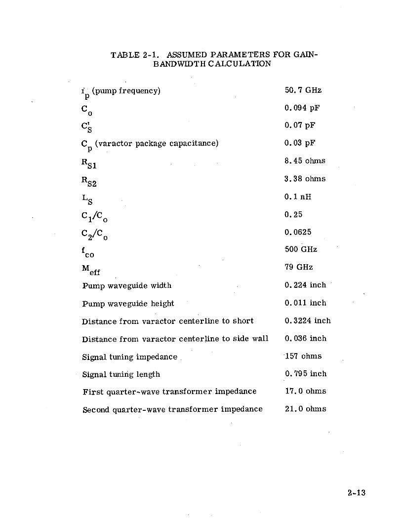
TABLE 2-1. ASSUMED PARAMETERS FOR GAIN-BANDWIDTH CALCULATION
i (pump frequency) 50. 7 GHzP
C 0.094 pF
C 0.07 pF
C (varactor package capacitance) 0.03 pFp
RS1 8.4 5 ohms
RS2 3.38 ohms
LS 0.1 nH
C1/C 0o 0.25
C 2/C o 0.0625
f 500 GHzco
M eff 79 GHz
Pump waveguide width 0. 224 inch
Pump waveguide height 0.011 inch
Distance from varactor centerline to short 0. 3224 inch
Distance from varactor centerline to side wall 0. 036 inch
Signal tuning impedance 157 ohms
Signal tuning length 0.795 inch
First quarter-wave transformer impedance 17. 0 ohms
Second quarter-wave transformer impedance 21.0 ohms
2-13
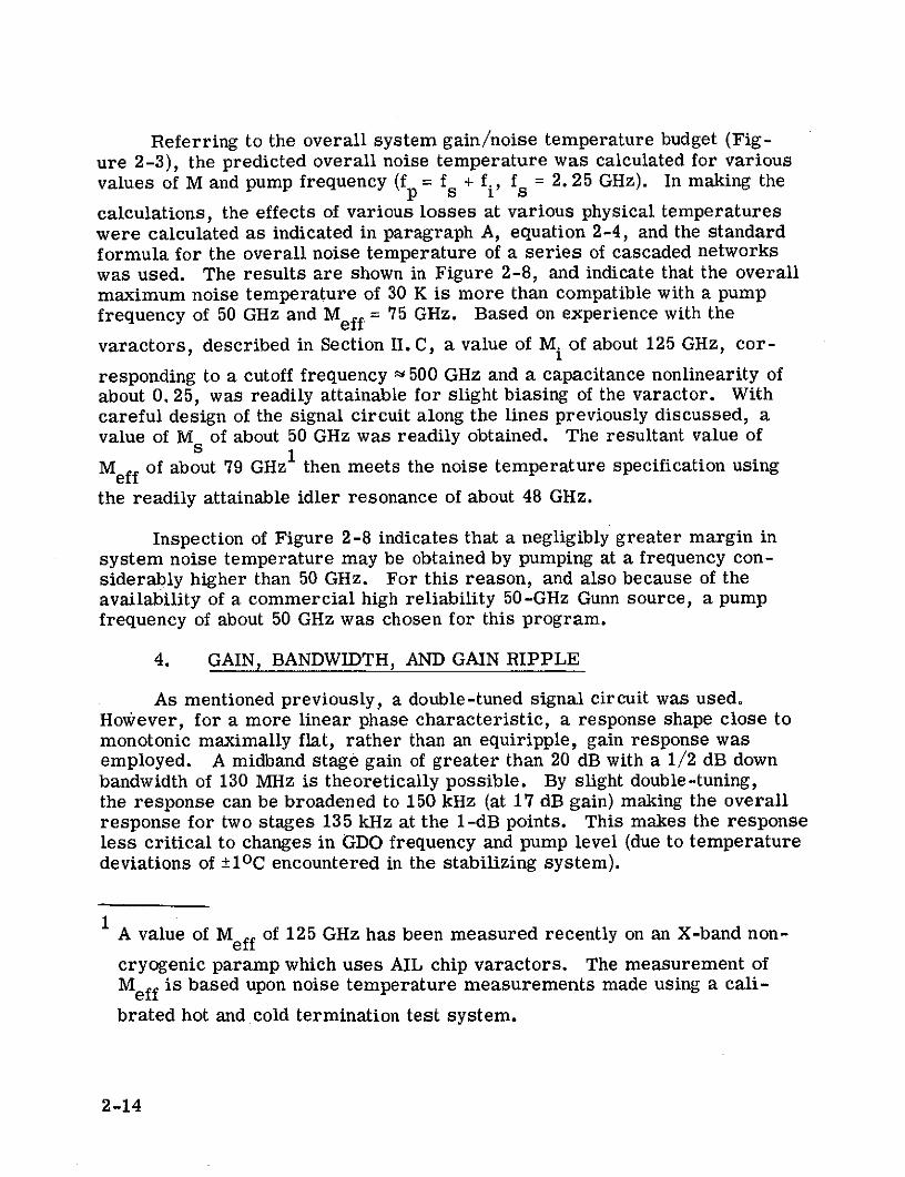
Referring to the overall system gain/noise temperature budget (Fig-ure 2-3), the predicted overall noise temperature was calculated for variousvalues of M and pump frequency (f = f + f f = 2. 25 GHz). In making the
calculations, the effects of various losses at various physical temperatureswere calculated as indicated in paragraph A, equation 2-4, and the standardformula for the overall noise temperature of a series of cascaded networkswas used. The results are shown in Figure 2-8, and indicate that the overallmaximum noise temperature of 30 K is more than compatible with a pumpfrequency of 50 GHz and M ef f = 75 GHz. Based on experience with the
varactors, described in Section II. C, a value of Mi of about 125 GHz, cor-
responding to a cutoff frequency 500 GHz and a capacitance nonlinearity ofabout 0.25, was readily attainable for slight biasing of the varactor. Withcareful design of the signal circuit along the lines previously discussed, avalue of M of about 50 GHz was readily obtained. The resultant value ofs
1M ef f of about 79 GHz then meets the noise temperature specification using
effthe readily attainable idler resonance of about 48 GHz.
Inspection of Figure 2-8 indicates that a negligibly greater margin insystem noise temperature may be obtained by pumping at a frequency con-siderably higher than 50 GHz. For this reason, and also because of theavailability of a commercial high reliability 50-GHz Gunn source, a pumpfrequency of about 50 GHz was chosen for this program.
4. GAIN, BANDWIDTH, AND GAIN RIPPLE
As mentioned previously, a double-tuned signal circuit was used.However, for a more linear phase characteristic, a response shape close tomonotonic maximally flat, rather than an equiripple, gain response wasemployed. A midband stage gain of greater than 20 dB with a 1/2 dB downbandwidth of 130 MHz is theoretically possible. By slight double-tuning,the response can be broadened to 150 kHz (at 17 dB gain) making the overallresponse for two stages 135 kHz at the 1-dB points. This makes the responseless critical to changes in GDO frequency and pump level (due to temperaturedeviations of ±10 C encountered in the stabilizing system).
A value of Meff of 125 GHz has been measured recently on an X-band non-eff
cryogenic paramp which uses AIL chip varactors. The measurement ofMeff is based upon noise temperature measurements made using a cali-
brated hot and cold termination test system.
2-14
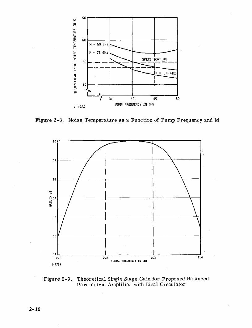
Appendix A summarizes the derivation of the paramp gain as a functionof frequency. Using the computer program and the parameters of Table 2-1,the gain response of Figure 2-3 was obtained for a stage gain level of 20 dB,which exceeds the minimum of 17 dB used in the gain-noise temperaturebudget of Figure 2-9.
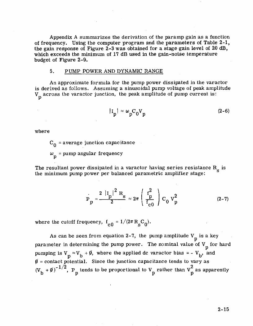
5. PUMP POWER AND DYNAMIC RANGE
An approximate formula for the pump power dissipated in the varactoris derived as follows. Assuming a sinusoidal pump voltage of peak amplitudeV across the varactor junction, the peak amplitude of pump current is:
P
I wCV (2-6)p pop
where
CO = average junction capacitance
w = pump angular frequencyP
The resultant power dissipated in a varactor having series resistance R isthe minimum pump power per balanced parametric amplifier stage:
2 111 Rs f CO V 2
P 2 T 2 C (2-7)p- 2 O p
where the cutoff frequency, f0 = 1/(2r RsC 0)
As can be seen from equation 2-7, the pump amplitude V is a keyP
parameter in determining the pump power. The nominal value of V for hardp
pumping is Vp Vb + 0, where the applied de varactor bias = - Vb, and
0 = contact potential. Since the junction capacitance tends to vary as1/2 2(V + 0) 1/2, p tends to be proportional to V rather than V as apparently
b p p p
2-15
50
W 40z M = 50 GHz
Li
"' M = 75 GHz *- .
SPECIFICATIONH 0
-20
z
30 40 50 60
4-1926 PUMP FREQUENCY IN GHz
Figure 2-8. Noise Temperature as a Function of Pump Frequency and M
19
20 "
iLi
18
17
HI
16
15
1412.1 2.2 2.3 2.4
SIGNAL FREQUENCY IN GHz
4-1759
Figure 2-9. Theoretical Single Stae a Gain for Proposed Balanced
Parametric Amplifier with Ideal Circulator
2-16
indicated by equation 2-7. Nevertheless, there is still a tradeoff to be con-sidered between pump power (or V ) and varactor figure of merit (M). In-
Pcreasing the bias and hence V and the pump power for hard pumping willalso increase both the cutoff frequency and nonlinearity ratio to increase M.In our experience, a bias of about -2.0 V is more than necessary to achievean M. of about 125 GHz. Thus, the pump power is calculated for V p3.0 V
1 p(0 1 V) yielding a value of P 27.4 mW for f = 50.7 GHz, f =500 GHz,
p p coand C = 0.094 pF. In paragraph E it is shown that over 33 mW of pump
0power is attainable which provides a good margin of safety, even for hardpumping.
Reference 1, equation 10. 65, gives the following simple relation be-tween dissipated pump power and input signal power level to cause a frac-tional change in gain (AK/K):
in3/2 sIAKP. ='P K3/2(f.)&K (2-8)in p f K
Using this value of P = 27.4 mW, K = 20 dB (conservative), f = 2.25 GHz,p 5
f = 50.7 GHz, and J K/K = 0.206 (corresponding to -1.0 dB gain com-p
pression) yields Pin = -46.0 dBm at the input to the amplifier, which meets
the dynamic range specification.
6. MEASURED SINGLE-STAGE PERFORMANCE
The following typical single-stage performance has been measured onthe prototype mounts:
Prototype Mount Serial No. B13 B15Gain, dB 15.0 15.0Center frequency, GHz 2.25 2.251 dB down bandwidth, MHz 130 120Response shape MonotonicRipple Less than 0.2 dBBias, Volts -1.9 -2.8Pump frequency, GHz 51.0 50.8
2-17
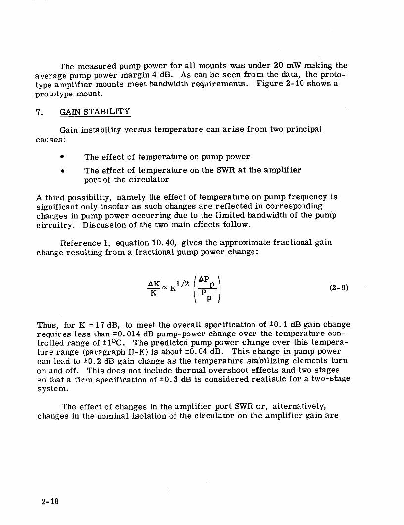
The measured pump power for all mounts was under 20 mW making theaverage pump power margin 4 dB. As can be seen from the data, the proto-type amplifier mounts meet bandwidth requirements. Figure 2-10 shows aprototype mount.
7. GAIN STABILITY
Gain instability versus temperature can arise from two principalcauses:
* The effect of temperature on pump power
* The effect of temperature on the SWR at the amplifierport of the circulator
A third possibility, namely the effect of temperature on pump frequency issignificant only insofar as such changes are reflected in correspondingchanges in pump power occurring due to the limited bandwidth of the pumpcircuitry. Discussion of the two main effects follow.
Reference 1, equation 10.40, gives the approximate fractional gainchange resulting from a fractional pump power change:
AK -K1/2 (2-9)K P
p
Thus, for K = 17 dB, to meet the overall specification of ±0. 1 dB gain changerequires less than ±0. 014 dB pump-power change over the temperature con-trolled range of ±1 0 C. The predicted pump power change over this tempera-ture range (paragraph II-E) is about ±0.04 dB. This change in pump powercan lead to ±0.2 dB gain change as the temperature stabilizing elements turnon and off. This does not include thermal overshoot effects and two stagesso that a firm specification of ±0.3 dB is considered realistic for a two-stagesystem.
The effect of changes in the amplifier port SWR or, alternatively,changes in the nominal isolation of the circulator on the amplifier gain are
2-18
4-1927
ID
Figure 2-10. Parametric Amplifier Mount
derived in Appendix B. The relevant formula is equation B-5 in Appendix B,which is repeated here for completeness:
AK IK 1/2 AL1K L. L. (2-10)
where L. is the nominal magnitude of port-to-port circulator isolation. As-1
suming a normal port isolation L 25 dB and K = 17 dB, leads to an allow-
able L./L i = ±25 dB for K/K = ±0. 1 dB. It is believed that this change in L1i 1
can easily be met with sufficient margin over a temperature range of ± 10lC.The resultant gain change due to this cause and pump power changes, con-sidered to add in an rms fashion. Since this effect is small compared toGunn oscillator power changes the total maximum gain changes to +0.3 dBis realistic.
The gain stability versus time specification is considered a less strin-gent specification than the gain stability versus temperature, and this wasmet by using stable temperature controlled mounting surfaces for theparamp circulators and GDO's.
8. SPURIOUS RESPONSES, IM PRODUCTS
A commonly used equation for predicting third-order intermodulationproducts (the principal ones usually consisting of outputs at frequencies
2f1 - f2 or 2f 2 - f1 , where fl and f2 are two closely separated signal fre-
quencies) is given below:
PIM = P1 + 2P2 + K21
where
PIM = output power at frequency 2f 2 - f 1 in dBm
P = output power at frequency fl in dBm
P2 = output power at frequency f2 f in dBm
K = third-order intermodulation product coefficient in dB21 (an alternative equation, interchanging subscripts 1
and 2 could also be written)
2-20
The key parameter in predicting IM performance is thus K2 1 . Pre-
vious experience at AIL for similar amplifiers employing chip varactorsyielded K 2 1 = +8 dB. Using a developed gain at midband of 33 dB in the speci-
fications, two -65 dBm signals in the 2200 to 2300 MHz band result in apredicted IM level of -88.0 dBm which is 53.0 dB belwo the output of eitherin-band signal output level. This, therefore, meets the 50 dB down require-ment and agrees reasonably well with the measured -51 dB value.
A filter has been incorporated to ensure that the pump leakage is at least-100 dBm at the output of the system. This filter must pass the signal bandnear 2.25 GHz with low loss and greatly attenuate the pump at about 50 GHz.
The form of this filter is a dual pair of radial chokes, each pair spacedone-quarter wavelength at 50 GHz. The measured signal frequency insertionloss of the filter is less than 0. 2 dB while the VSWR is better than 1. 15. Thetwo pairs are separated by one-quarter wavelength at the signal circuit fre-quency. The measured performance of this filter shows greater than 60-dBrejection at the 50. 7-GHz pump frequency. The minimum rejection of thepump frequency due to the balanced paramp configuration, coaxial links, cir-culator, and isolator is greaterthan 50 dB. Compliance with the spuriousoutput requirement of greater than a 60 dB below the desired response witha -65 dBm input signal is possible for the calculated pump level of +14.3 dBm(27.4 mW in paragraph II-B-5). The actual spurious level could not be mea-sured because of limited sensitivity of the spectrum analyzer. No spuriouscould be detected at -85 dBm which was the limit of the analyzer sensitivity.
9. PHASE STABILITY
As for gain, phase instabilities arise from pump-power changes. Pumpfrequency changes, however, are even more important and the situation iscomplicated by the passband characteristics (single or double tuned). Ac-tually, the gain instability calculations in paragraph II-B-7 previously weredone for midband, without regard to the passband shape. Extensive theoretical
2-21
analyses have been made at AIL of both gain and phase changes for single,double, and triple tuned maximally flat responses as a function of pump-
power and frequency changes. However, correlation with experiment hasnot been attempted and it was not deemed worthwhile to include these anal-
yses here. Suffice it to say that the long-term phase stability specificationof +5 degrees across the passband was met when the temperature controlled
enclosure is constant enough in temperature to minimize pump-power andfrequency changes.
10. PHASE LINEARITY AND VARIATION OF PHASE LINEARITY
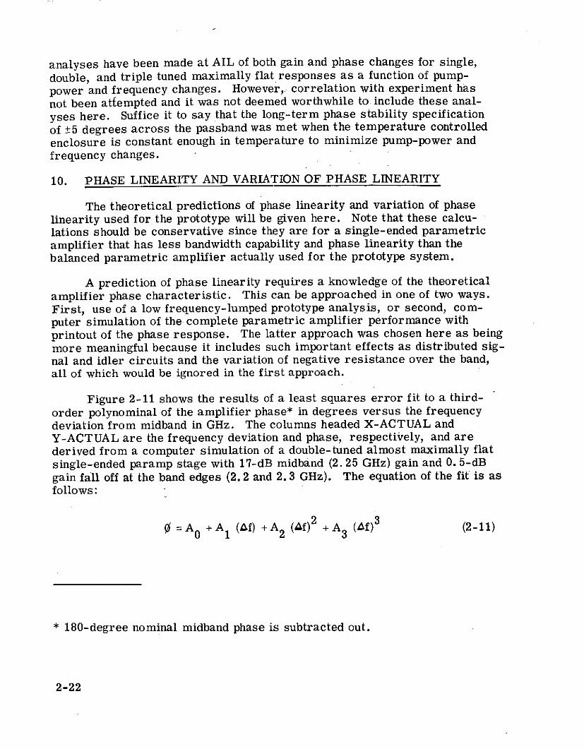
The theoretical predictions of phase linearity and variation of phaselinearity used for the prototype will be given here. Note that these calcu-lations should be conservative since they are for a single-ended parametricamplifier that has less bandwidth capability and phase linearity than thebalanced parametric amplifier actually used for the prototype system.
A prediction of phase linearity requires a knowledge of the theoreticalamplifier phase characteristic. This can be approached in one of two ways.First, use of a low frequency-lumped prototype analysis, or second, com-puter simulation of the complete parametric amplifier performance withprintout of the phase response. The latter approach was chosen here as beingmore meaningful because it includes such important effects as distributed sig-nal and idler circuits and the variation of negative resistance over the band,all of which would be ignored in the first approach.
Figure 2-11 shows the results of a least squares error fit to a third-order polynominal of the amplifier phase* in degrees versus the frequencydeviation from midband in GHz. The columns headed X-ACTUAL andY-ACTUAL are the frequency deviation and phase, respectively, and arederived from a computer simulation of a double-tuned almost maximally flatsingle-ended paramp stage with 17-dB midband (2.25 GHz) gain and 0. 5-dBgain fall off at the band edges (2.2 and 2.3 GHz). The equation of the fit is asfollows:
0 = A 0 + A 1 (Af) +A 2 (&f) 2 + A (f) 3 (2-11)
* 180-degree nominal midband phase is subtracted out.
2-22
where, from Figure 2-11:
A 0 = 0.06
A 1 = 952.2
A 2 = 577.4
A 3 = -10150
From equation 2-11, the deviation from a linear phase characteristicis:
0- A 0 - A 1 (Af) = A2 (&f) 2 + A3 (Af) 3 (2-12)
Considering the signs of A2 and A 3 , the maximum positive deviation from
linear phase will occur for the largest negative value of Af. Thus, for thecenter 60-MHz specification, the worst case is 4f = -0.03 GHz, and for theband-edge specification, the worst case is Af = -0. 05 GHz. Substitutingnumerical values in equation 2-12 yields corresponding maximum phase de-viations of +0.8 and +2.7 degrees, respectively. Furthermore, since thedeviation from linear phase is still positive at the upper band edge (Af =+0.05 GHz), the maximum "negative" deviation from linear phase occurs atmidband (Af = 0) and equals 0. * The total greatest phase deviations fromlinearity for two identical stages, therefore, calculates to be 1. 6 and 5. 4 de-grees for the center and band-edge frequency regions, respectively, com-pared to the specifications of 10 and 15 degrees.
Differentiating, equation 2-11 yields the rate of change of phase withfrequency:
dO A +2A (f) + 3A (f) 2 (2-13)df 1 2
* For the ideal symmetrical parabolic envelope delay characteristic,A = 0 and the maximum positive and negative deviations from linear
phase would be equal and occur at the band edges.
2-23
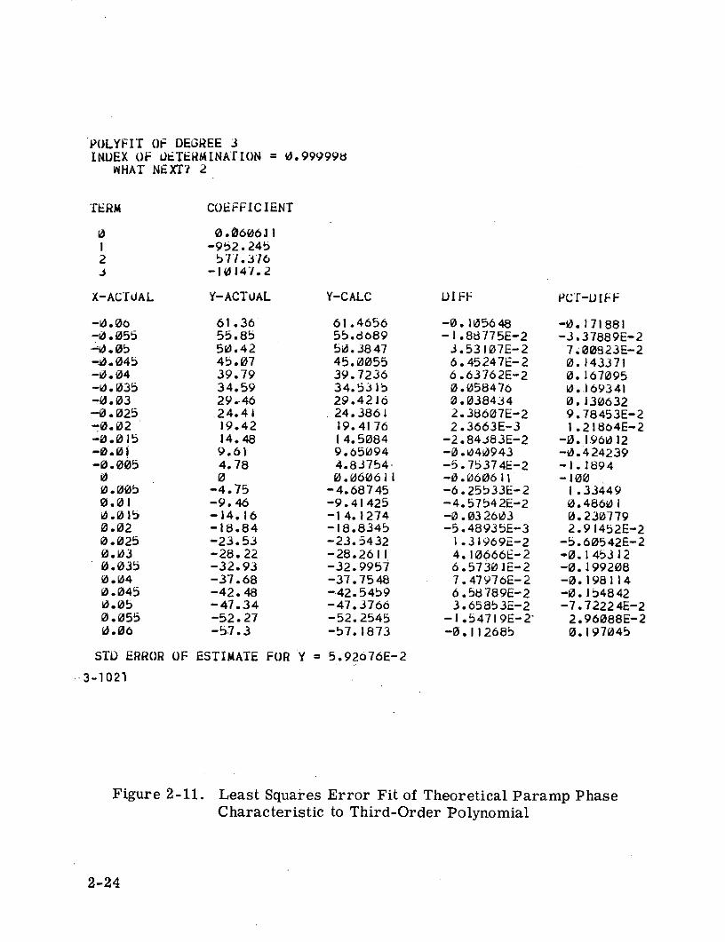
POLYFIT OF DEGREE 3INDEX OF UETERMINATION = 0.999998
WHAT NEXT? 2
TERM COEFFICIENT
0 0.0606JII -952.2452 571.3764 -10147.2
X-ACTUAL Y-ACTUAL Y-CALC DIFF PCT-UIFF
-0.00 61.36 61.4656 -0.105648 -0.171881-0.055 55.85 55.8089 -1.88775E-2 -3.37889E-2-0.05 50.42 50.3847 3.53107E-2 7.00823E-2-0.045 45.07 45.0055 6.45247E-2 0.143371-0.04 39.79 39.7236 6.63762E-2 0.167095-0.035 34.59 34.531b 0.058476 0.169341-0.03 29.-46 29.4216 0.038434 0.130632-0.025 24.41 .24.3861 2.38607E-2 9.78453E-2-0.02 19.42 19.4176 2.3663E-3 I1.21864E-2-0.015 14.48 14.5084 -2.84J83E-2 -0.196012-0.01 9.61 9.65094 -0.040943 -0.424239-0.005 4.78 4.83754 -5.75374E-2 -1.18940 0 0.060611 -0.060611 -1000.005b -4.75 -4.68745 -6.25533E-2 1.334490.01 -9.46 -9.41425 -4.57542E-2 0.486010.015 -14.16 -14.1274 -0.032603 0.2307790.02 -18.84 -18.8345 -5.48935E-3 2.91452E-20.025 -23.53 -23.5432 1.31969E-2 -5.60542E-20.03 -28.22 -28.2611 4.10666E-2 -0.1453120.035 -32.93 -32.9957 6.57301E-2 -0.1992080.04 -37.68 -37.7548 7.47976E-2 -0.1981140.045 -42.48 -42.5459 6.58789E-2 -0.1548420.05 -47.34 -47.3766 3.65853E-2 -7.72224E-20.055 -52.27 -52.2545 -1.54719E-2 2.96088E-20.06 -57.3 -57.1873 -0.112685 0.197045
STD ERROR OF ESTIMATE FOR Y = 5.92o76E-2
3-1021
Figure 2-11. Least Squares Error Fit of Theoretical Paramp PhaseCharacteristic to Third-Order Polynomial
2-24
It is understood that the specification of maximum rate of change of phasewith frequency of 0. 5-degree/MHz refers to the maximum rate of changewith frequency of the deviation of phase from a linear phase characteristic.This latter quantity is given by the derivative of equation 2-12 which isequation 2-13 minus the constant term A 1 .
The worst case is for Af = 0.05 GHz, which yields a value of 0.13 de-gree/MHz. Doubling this value for two identical stages yields 0. 27 degree/MHz compared to the specification of 0. 5 degree/MHz.
2-25
C. VARACTOR
1. GENERAL
Over the past 10 years the Central Research Group of AIL has beenengaged in varactor research. The goal has been to make varactors whichhave very high cutoff frequencies and at the same time have very low para-sitic elements. This work was supported by AIL using internal researchand development funds.
Both Schottky barrier (metal semiconductor) and P-N junction varac-tors having zero-bias cutoff frequencies in excess of 600 GHz with typicalzero-bias capacities of 0. 15 pF have been successfully fabricated duringthis period. The major development effort has been concentrated onSchottky barrier varactors since they offer advantages in ease of fabrication(fewer steps) and inherently lower series resistance.
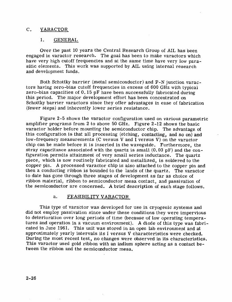
Figure 2-5 shows the varactor configuration used on various parametricamplifier programs from 2 to above 50 GHz. Figure 2-12 shows the basicvaractor holder before mounting the semiconductor chip. The advantage- ofthis configuration is that all processing (etching, contacting, and so on) andlow-frequency measurements (C versus V and I versus V) on the varactorchip can be made before it is inserted in the waveguide. Furthermore, thestray capacitance associated with the quartz is small (0.03 pF) and the con-figuration permits attainment of very small series inductance. The quartzpiece, which is now routinely fabricated and metallized, is soldered to thecopper pin. A processed varactor chip is also attached to the copper pin andthen a conducting ribbon is bounded to the lands of the quartz. The varactorto date has gone through three stages of development as far as choice ofribbon material, ribbon to semiconductor mesa contact, and passivation ofthe semiconductor are concerned. A brief description of each stage follows.
a. FEASIBILITY VARACTOR
This type of varactor was developed for use in cryogenic systems anddid not employ passivation since under these conditions they were imperviousto deterioration over long periods of time (because of low operating tempera-tures and operation in a vacuum environment). A diode of this type was fabri-cated in June 1961. This unit was stored in an open lab environment and atapproximately yearly intervals its I versus V characteristics were checked.During the most recent test, no changes were observed in its characteristics.This varactor used gold ribbon with an indium sphere acting as a contact be-tween the ribbon and the semiconductor mesa.
2-26
METALLIZED QUARTZLAND
SOLDER BOND
CHIP MOUNTINGAREA COPPER
PIN
Y70-"7
Figure 2-12. Varactor Holder
b. PROTOTYPE VARACTOR
This varactor was developed to allow use in paramps that had to bestabilized at temperatures up to 50oC. The indium-gold contact of the feasi-bility varactor was found to gradually diffuse at these temperatures. Aplatinum ribbon was substituted for the gold to overcome this problem.Like a feasibility varactor, this was not passivated.
c. QUANAR VARACTOR
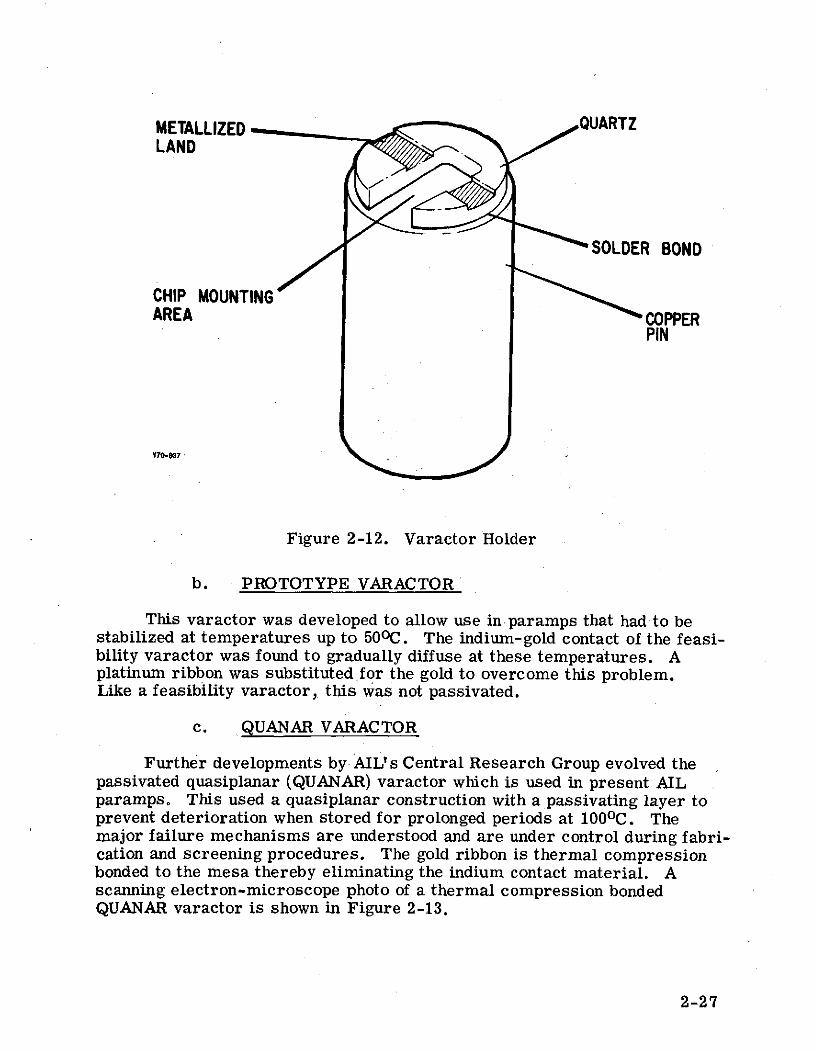
Further developments by AIL's Central Research Group evolved thepassivated quasiplanar (QUANAR) varactor which is used in present AILparamps. This used a quasiplanar construction with a passivating layer toprevent deterioration when stored for prolonged periods at 100 0 C. Themajor failure mechanisms are understood and are under control during fabri-cation and screening procedures. The gold ribbon is thermal compressionbonded to the mesa thereby eliminating the indium contact material. Ascanning electron-microscope photo of a thermal compression bondedQUANAR varactor is shown in Figure 2-13.
2-27
ROP QUCIBI ITY OF THEORIGLNAL PAGE IS POOR
Figure 2-13. Assembled Quanar Varactor
2-28
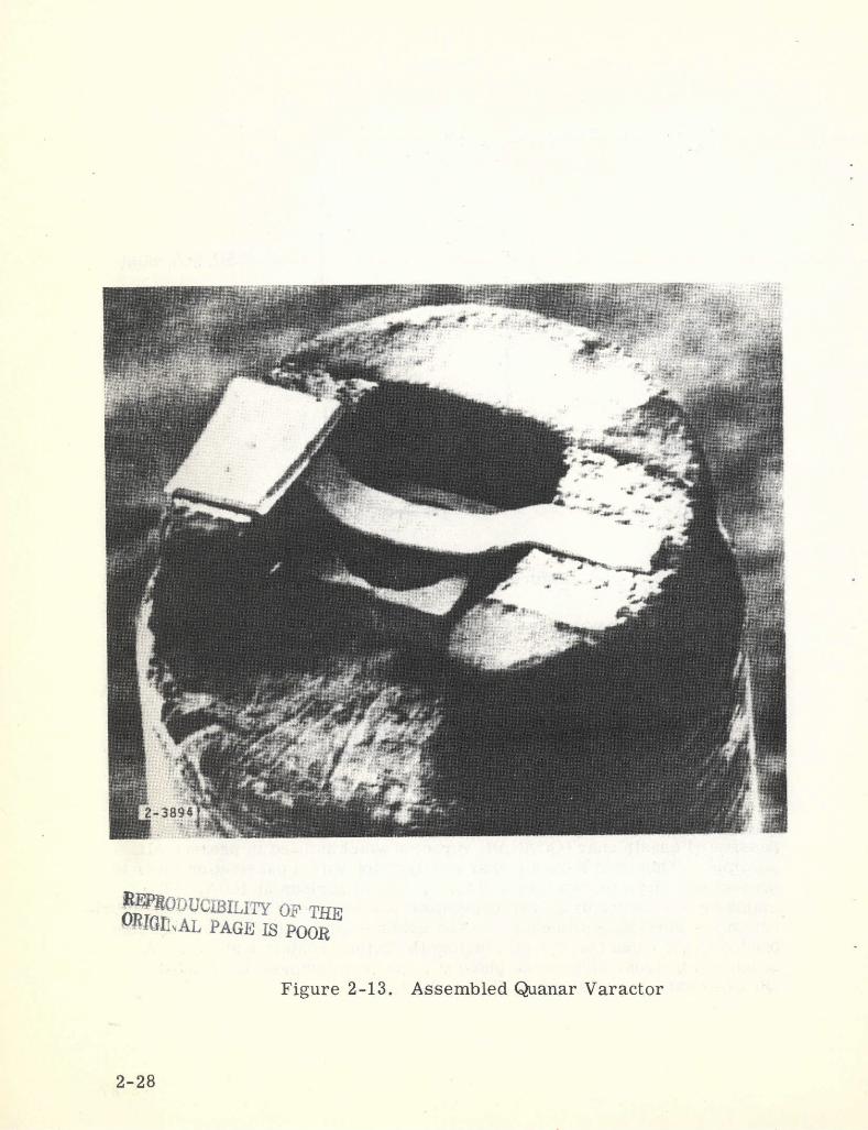
2. CHARACTERIZATION MEASUREMENTS OF VARACTORS
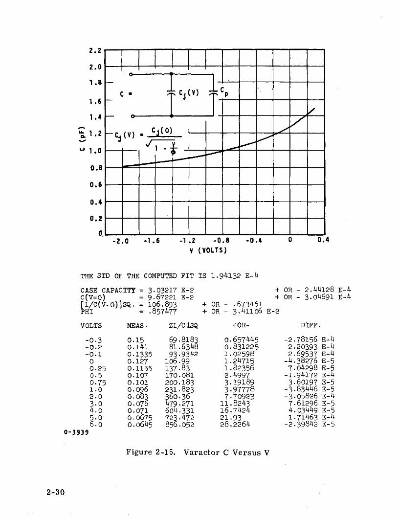
Two low-frequency measurements are made on the varactor before itis inserted into a mount; namely, current versus voltage (I versus V) andcapacitance versus voltage (C versus V). The I versus V data for a typicalvaractor is shown in Figure 2-14. This measurement is made on a Tek-tronix Type 575 Transistor Curve Tracer. Both the reverse breakdownvoltages (Vb) at 1 and 10 uA and the forward voltage (Vf) for 0.1 and 10 uA
are noted. Since the current between these forward and reverse conduction
voltages can be as small as 10 - 1 2 A, the curve tracer shows no current exceptnear the conduction points. However, a General Radio Type 1230A electro-
meter, which is capable of measuring 10-13A, is employed to make I versusV measurements on selected units.
A Boonton Model 75D Capacitance Bridge is used to make C versus Vmeasurements. The maximum ac voltage across the varactor during themeasurement is 15 mV. A direct reading of C versus V is obtained fromthe bridge and this data is then computer processed as shown in Figure 2-15.The extraneous capacitance across the varactor, the built-in (contact) poten-tial of the varactor, and the actual C versus V of the varactor are all calcu-lated by the computer.
I 0 FA At
- +
0-3938RI 0 I VOLT
Figure 2-14. Typical Varactor I Versus V Trace
2-29
2.2-
2.0
'~1.0
1.8 -- c - ,sc (v) -<cp
1.6--
1.2 -C (V) . C (0)
0.8 -
0.6
0.4
0,.2
-2.0 -1.6 -1 .2 -0.8 -0.4 o.4
V (VOLTS)
THE STD OF THE COMPUTED FIT IS 1.94132 E-4
CASE CAPACITY = 3.03217 E-2 + OR - 2.44128 E-4c(v=o) = 9.67221 E-2 + OR - 3.04691 E-4[1/c(v-o)]sQ. = 106.893 + OR - .673461PHI = .857477 + OR - 3.41106 E-2
VOLTS MEAS. Zl/ClISQ +OR- DIFF.
-0.3 0.15 69.8183 0.657445 -2.78156 E-4-0.2 0.141 81.6348 0.831225 2.20393 E-4-0.1 0.1335 93.9342 1.02598 2.69537 E-40 0.127 106.99 1.24715 -4.38276 E-50.25 0.1155 137.83 1.82356 7.04298 E-50.5 0.107 170.081 2.4997 -1.94172 E-40.75 0.101 200.183 3.19189 3.60197 E-51.0 0.096 231.823 3.97778 -3.83446 E-52.0 0.083 360.36 7.70923 -3.05826 E-43.0 0.076 479.271 11.8243 7.61296 E-54.0 0.071 604.331 16.7424 4.03449 E-55.0 0.0675 723.472 21.93 1.71463 E-46.0 0.0645 856.052 28.2264 -2.39842 E-5
0-3939
Figure 2-15. Varactor C Versus V
2-30
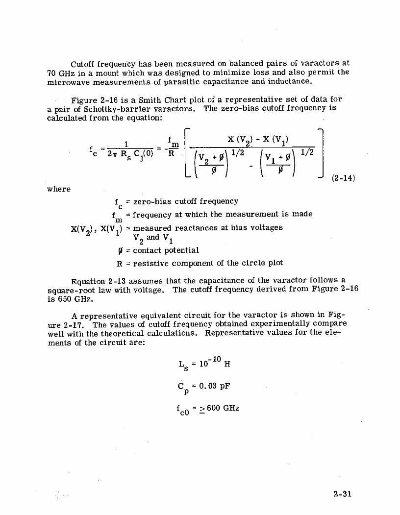
Cutoff frequency has been measured on balanced pairs of varactors at
70 GHz in a mount which was designed to minimize loss and also permit the
microwave measurements of parasitic capacitance and inductance.
Figure 2-16 is a Smith Chart plot of a representative set of data for
a pair of Schottky-barrier varactors. The zero-bias cutoff frequency iscalculated from the equation:
1 fm X(V 2 )-X(V)
1/2 01/2where(0) RL V2 )1/2 (V1- (2-14)
where
f = zero-bias cutoff frequencyc
f = frequency at which the measurement is madem
X(V2 ), X(V 1) = measured reactances at bias voltagesV 2 and V1
0 = contact potential
R = resistive component of the circle plot
Equation 2-13 assumes that the capacitance of the varactor follows a
square-root law with voltage. The cutoff frequency derived from Figure 2-16is 650 GHz.
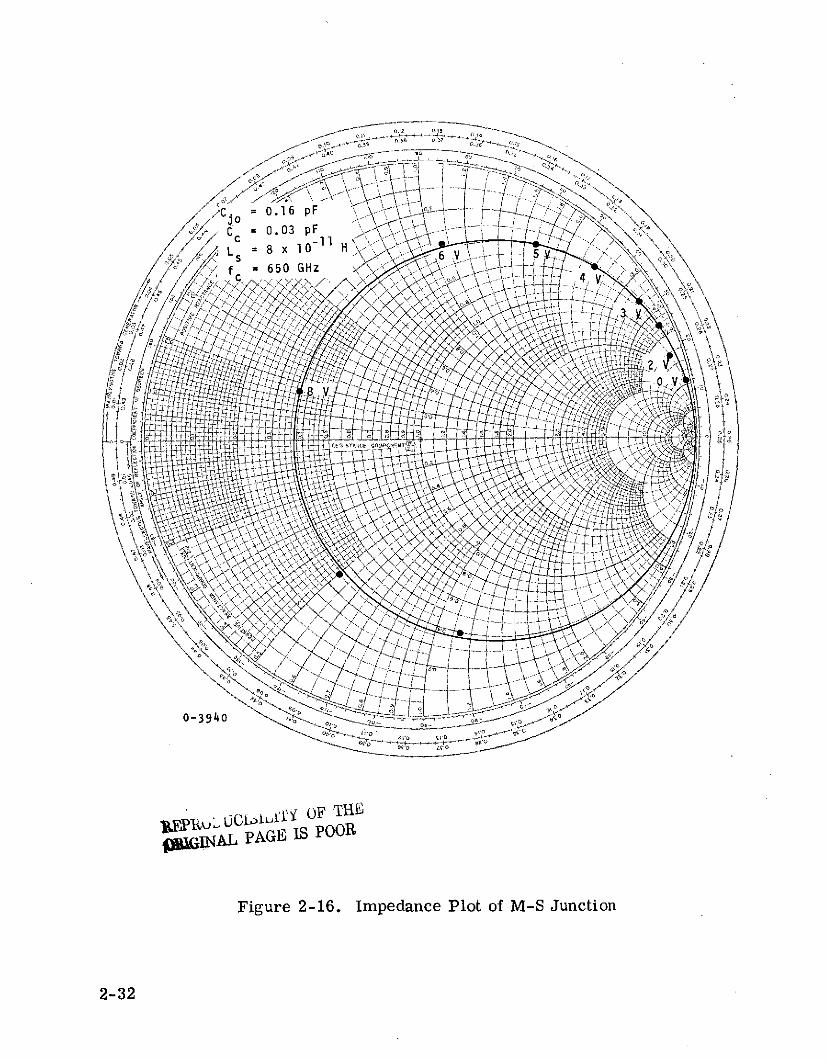
A representative equivalent circuit for the varactor is shown in Fig-
ure 2-17. The values of cutoff frequency obtained experimentally compare
well with the theoretical calculations. Representative values for the ele-ments of the circuit are:
10L = 10 H
C = 0.03 pF
fc = > 600 GHz
2-cO31
2-31
0-104
lt,,FP~gu UCOi- i OFTH
NAL PAGE IS POOR
Figure 2-16. Impedance Plot of M-S Junction
2-32
WHERE:-
C. = JUNCTION CAPACITANCE3L SLS = STRAY INDUCTANCER0 = SERIES RESISTANCE Cp C.
Cp = STRAY CAPACITANCE RESULTING ROFROM METALLIZED LAND
3-1022
Figure 2-17. Equivalent Circuit of Chip Varactor and Holder
Typically, the reverse breakdown voltage of the varactors is greaterthan 10 V. The fabrication techniques permit making varactors with a zero-bias junction capacitance greater than 0.07 pF and a capacitance versus volt-age law that is square root, with contact potential of:
0 = 0.9 V
Based on these considerations, the nominal electrical specifications ofthe paramp varactor is as follows:
* Operating junction capacitance 0. 12 + 0. 005 pF
* Operating cutoff frequency > 600 GHz
* Reverse breakdown (at 1 pA) > 10 V
* Stray capacitance 0.03 ± 0.01 pF
* Lead inductance 10-10 H (nominal)
* Nonlinearity Square law
* Maximum power dissipation 50 mW
3. EVALUATION OF UNPASSIVATED VARACTORS
The results of evaluation tests on the unpassivated feasibility and proto-type varactors are described in this paragraph. These varactors were sub-ject to the evaluation test procedure given in Appendix D. A summary of thetest results follows.
2-33
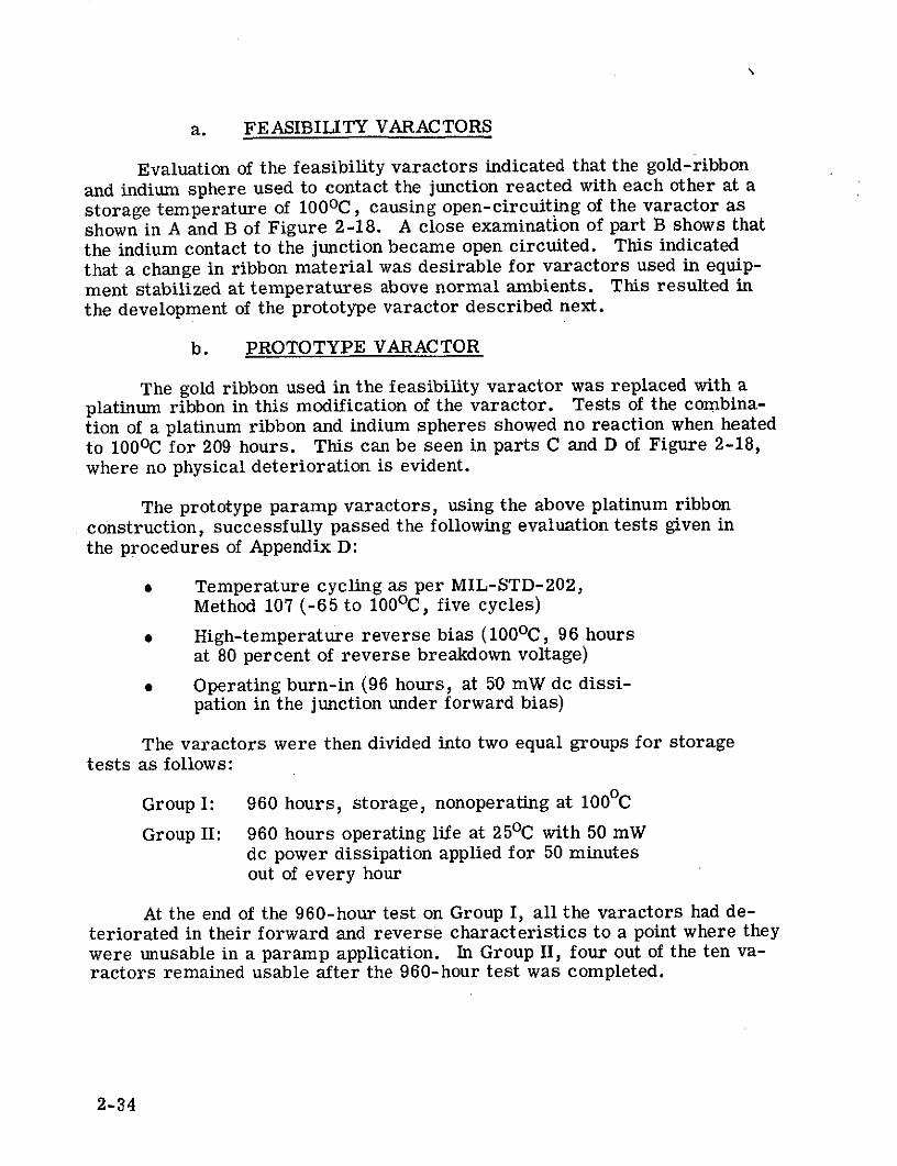
a. FEASIBILITY VARACTORS
Evaluation of the feasibility varactors indicated that the gold-ribbon
and indium sphere used to contact the junction reacted with each other at a
storage temperature of 100 0 C, causing open-circuiting of the varactor asshown in A and B of Figure 2-18. A close examination of part B shows that
the indium contact to the junction became open circuited. This indicatedthat a change in ribbon material was desirable for varactors used in equip-ment stabilized at temperatures above normal ambients. This resulted inthe development of the prototype varactor described next.
b. PROTOTYPE VARACTOR
The gold ribbon used in the feasibility varactor was replaced with aplatinum ribbon in this modification of the varactor. Tests of the combina-tion of a platinum ribbon and indium spheres showed no reaction when heatedto 100 0 C for 209 hours. This can be seen in parts C and D of Figure 2-18,where no physical deterioration is evident.
The prototype paramp varactors, using the above platinum ribbonconstruction, successfully passed the following evaluation tests given inthe procedures of Appendix D:
* Temperature cycling as per MIL-STD-202,Method 107 (-65 to 100 0 C, five cycles)
* High-temperature reverse bias (100 0 C, 96 hoursat 80 percent of reverse breakdown voltage)
* Operating burn-in (96 hours, at 50 mW dc dissi-pation in the junction under forward bias)
The varactors were then divided into two equal groups for storagetests as follows:
Group I: 960 hours, storage, nonoperating at 100 0 C
Group II: 960 hours operating life at 25 0 C with 50 mWde power dissipation applied for 50 minutesout of every hour
At the end of the 960-hour test on Group I, all the varactors had de-teriorated in their forward and reverse characteristics to a point where theywere unusable in a paramp application. In Group II, four out of the ten va-ractors remained usable after the 960-hour test was completed.
2-34
A. PRIOR TO BAKE FEASIBILITY C. PRIOR TO BAKE ETM VARACTORVARACTOR (GOLD RIBBON) (PLATINUM RIBBON)
B. AFTER 150 HOURS AT 101* C D. AFTER 209 HOURS AT 1010 C ETMFEASIBILITY VARACTOR (GOLD RIBBON) VARACTOR (PLATINUM RIBBON)
1-5376
Figure 2-18. Effect of Temperature on Varactor Contact
The results of an intensive study of these tests by AIL's Central Re-search Group indicated that the basic problem was surface diffusion of theindium contact material at 1000C which caused a gradual increase in for-ward conduction, eventually shorting out the junction. This was confirmedby etching away the indium, which restored the original varactor charac-teristics.
In order to overcome the temperature limitations, a quasiplanarvaractor was developed with SiO 2 passivation which greatly reduces the dif-
fusion rate at 1000C. In these varactors, the indium used to contact the mesato the ribbon has been replaced by a thermal-compression bond of the goldribbon to the mesa, thereby eliminating one potential source of failure.
A set of 20 of the thermal-compression bonded quasiplanar varactorswere fabricated. These were subjected to the same evaluation tests as theprototype varactor. The results of these tests are given in detail in the nextpart of the report.
A check of the cutoff frequency of the quasiplanar varactors at 70 GHzshowed that there was no degradation in cutoff frequency over the prototypevaractors.
4. EVALUATION TEST RESULTS--QUANAR VARACTORS
The results of evaluation tests performed on the AIL "QUANAR" passi-vated, thermal-compression bonded varactor, described previously, will bepresented in this paragraph. The evaluation procedure used for these testsis given in Appendix D along with sample data sheets. Initially, a total of28 QUANAR thermal-compression bonded varactors was fabricated for eval-uation purposes. Initially, the V versus I and C versus V characteristics ofthe varactors were measured. As a screening test they were subject to a24-hour nonoperating bake at 150 0 C. The varactors were then thermallyshocked from -65 to 100 0 C (five cycles). Upon measurement of the V versusI and C versus V characteristics, no deterioration was observed in any ofthe varactors with the exception of three units which were open due to de-fective thermal-compression bonds.
Twenty of these varactors were then subjected to the evaluation proce-dure given in Appendix D. A summary of the results of these tests is givenin Table 2-2 with copies of the data given for each varactor in Appendix E.
2-36
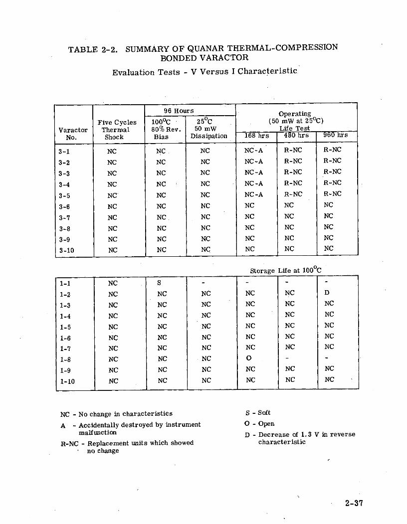
TABLE 2-2. SUMMARY OF QUANAR THERMAL-COMPRESSIONBONDED VARACTOR
Evaluation Tests - V Versus I Characteristic.
96 Hours Operating
Five Cycles 100 0 C 25 0 C (50 mW at 25 0 C)
Varactor Thermal 80% Rev. 50 mW Life TestNo. Shock Bias Dissipation 168 hrs 480 hrs 960 hrs
3-1 NC NC NC NC-A R-NC R-NC
3-2 NC NC NC NC-A R-NC R-NC
3-3 NC NC NC NC-A R-NC R-NC
3-4 NC NC NC NC-A R-NC R-NC
3-5 NC NC NC NC-A R-NC R-NC
3-6 NC NC NC NC NC NC
3-7 NC NC NC NC NC NC
3-8 NC NC NC NC NC NC
3-9 NC NC NC NC NC NC
3-10 NC NC NC NC NC NC
Storage Life at 1000C
1-1 NC S - - - -
1-2 NC NC NC NC NC D
1-3 NC NC NC NC NC NC
1-4 NC NC NC NC NC NC
1-5 NC NC NC NC NC NC
1-6 NC NC NC NC NC NC
1-7 NC NC NC NC NC NC
1-8 NC NC NC O - -
1-9 NC NC NC NC NC NC
1-10 NC NC NC NC NC NC
NC - No change in characteristics S - Soft
A - Accidentally destroyed by instrument O - Openmalfunction D - Decrease of 1.3 V in reverse
R-NC - Replacement units which showed characteristicno change
2-37
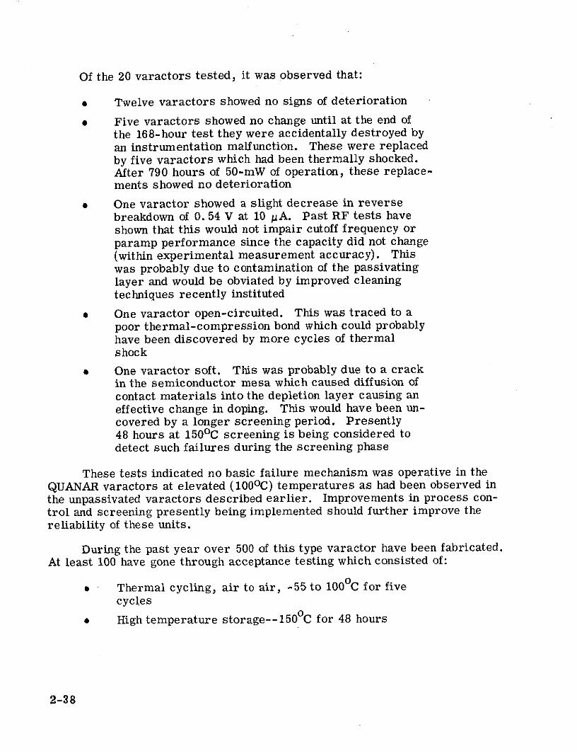
Of the 20 varactors tested, it was observed that:
* Twelve varactors showed no signs of deterioration
* Five varactors showed no change until at the end ofthe 168-hour test they were accidentally destroyed byan instrumentation malfunction. These were replacedby five varactors which had been thermally shocked.After 790 hours of 50-mW of operation, these replace-ments showed no deterioration
* One varactor showed a slight decrease in reversebreakdown of 0. 54 V at 10 pA. Past RF tests haveshown that this would not impair cutoff frequency orparamp performance since the capacity did not change(within experimental measurement accuracy). Thiswas probably due to contamination of the passivatinglayer and would be obviated by improved cleaningtechniques recently instituted
* One varactor open-circuited. This was traced to apoor thermal-compression bond which could probablyhave been discovered by more cycles of thermalshock
* One varactor soft. This was probably due to a crackin the semiconductor mesa which caused diffusion ofcontact materials into the depletion layer causing aneffective change in doping. This would have been un-covered by a longer screening period. Presently48 hours at 150 0 C screening is being considered todetect such failures during the screening phase
These tests indicated no basic failure mechanism was operative in theQUANAR varactors at elevated (100 0 C) temperatures as had been observed inthe unpassivated varactors described earlier. Improvements in process con-trol and screening presently being implemented should further improve thereliability of these units.
During the past year over 500 of this type varactor have been fabricated.At least 100 have gone through acceptance testing which consisted of:
* Thermal cycling, air to air, -55 to 100 0 C for fivecycles
* High temperature storage--1500 C for 48 hours
2-38
High temperature reverse bias--a reverse bias of8 V is applied at 150 0 C for 48 hours in accordancewith MIL-STD-750 Method 1038 Condition A
* Thermal shock--liquid to liquid 0 to 100 0 C for15 cycles in accordance with MIL-STD-750Method 1056
* Mechanical shock--five shocks in both directions ofeach axis at 1500G for 0. 5 ms in accordance withMIL-STD-750 Method 2016
* Power burn-in varactors are subjected alternatelyat a 60-Hz rate to 100-mW power dissipation in theforward direction then 8 V reverse bias for 168 hours
Only one failure occurred during the above testing. This unit becamesoft in the reverse direction and a SEM examination showed a cracked mesadue to the TC bond being made on the edge of the mesa. Ten varactors are
being given additional testing as follows:
* Thermal shock as above for an additional 20 cycles
* Mechanical shock as above
* Operating life test--the power burn-in described above
These varactors were tested after 250 hours and have since undergone
thousands of additional hours of testing. Another group of five varactors have
been subjected to the Moisture Resistance Test, Method 1021 of MIL-STD-750
with no changes occurring.
5. JUNCTION TEMPERATURE
The AIL Central Research Group has developed varactors having over600 GHz cutoff frequency and low parasitic reactances for application in high
performance parametric amplifiers. The QUANAR varactors have reached a
stage of development where they have been passivated to make them impervious
to most contaminants. Evaluation tests reported herein indicate that the va-
ractors are capable of operation at 150 0 C junction temperature for prolonged
periods without significant deterioration in characteristics. Thermal resist-
ance measurements have shown the thermal resistance to be an average of0. 8 mW/oC. Based on this, the maximum safe power dissipation for themaximum stabilization temperatures of 160 0 F and pump power level of 18 mW
per varactor, the junction operating temperature of the paramp varactors
would be 80 0 C or about 55 percent of the maximum rating. This is consid-
ered safe for long-term unattended operation. The previous series of tests
show the direct applicability of the varactor to successfully meet all of the
requirements of the program.
2-39
D. CIRCULATOR
1. GENERAL
One of the key parameters in the design of parametric amplifiers isthe circulator. In noncryogenic system operation, the circulator is respon-sible for a severe degradation of the basic amplifier's low-noise properties.For this reason, considerable effort has been directed toward improvingthe circulator loss characteristic during the last few years.
Since most of the losses are inherent to the physical properties of theferrite material, only limited improvements are to be expected in the nearfuture. The loss of the breadboard prototype circulator covering the 2. 20 to2.30 GHz band is 0. 1-dB per pass. This loss is assumed in the gain/noisetemperature budget discussed earlier.
2. CIRCULATOR DESIGN
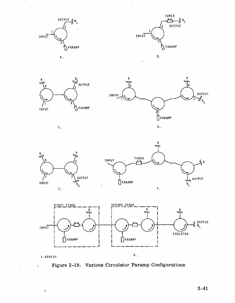
The basic circulator configurations are shown in Figure 2-19.
Let the circulator isolation per pass and the gain of the amplifier asa ratio or in decibels be indicated as L. or L.(dB and K or K respec-
1 L(dB) (dB)'tively.
If Li n+1) is the isolation between the nth and the (n + 2 )th port of athcirculator (circulating in the direction of increasing n) with the (n + 1 )
port terminated in a load R, the VSWR (S) of the terminated port with respectto R is very closely given by:
1+ [L.~l -1/2
S = (n + 1) (2-15)
(n + 1)1 Li(n+l) -1 /2
In the configuration of Figure 2-19, the maximum possible effectiveinput VSWR is then given by:
SZ S (2-16)1 1 Kmax 1-
32-40
2-40
TUNEROUTPUT R RL
3 3 OUTPUT
INPUT INPUT .2 2
PARAMP PARAMP
A. B.
R RL R R
4 3OUTPUT 5 4
INPUOUTPUT
2 3 R1 2 RL
INPUT PARAMP
PARAMP
C. D.
R
R R
4 3 INPUT TUNER R
1 2 OUTPUT OUTPUT
INPUT RL PARAMPRL
E. F.
FIRST STAGE SECOND STAGE
r- R 1R R
OUTPUT
INPUT RL
I I ISOLATOR
PARAMP PARAMPI I I
1-4840 Ri G.
Figure 2-19. Various Circulator Paramp Configurations
2-41
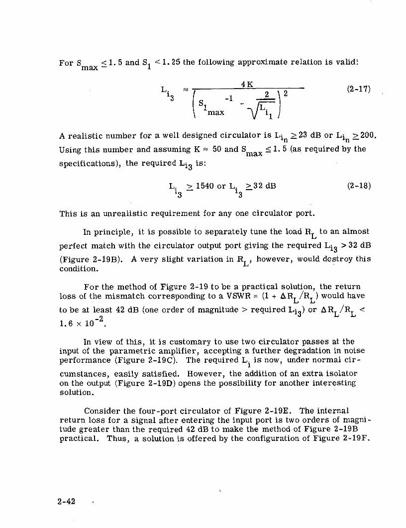
For Smax <1. 5 and S1 <1.25 the following approximate relation is valid:
4KL. )2 (2-17)
1 max i
A realistic number for a well designed circulator is Lin >23 dB or Li > 200.
Using this number and assuming K ; 50 and S ma x 1. 5 (as required by the
specifications), the required Li 3 is:
L. > 1540 or L. > 32 dB (2-18)13 - 13 -
This is an unrealistic requirement for any one circulator port.
In principle, it is possible to separately tune the load RL to an almost
perfect match with the circulator output port giving the required Li 3 > 32 dB
(Figure 2-19B). A very slight variation in RL, however, would destroy thiscondition.
For the method of Figure 2-19 to be a practical solution, the returnloss of the mismatch corresponding to a VSWR = (1 + ARL /R L ) would have
to be at least 42 dB (one order of magnitude > required Li 3 ) or ARL/RL <-2
1.6 x 10 .
In view of this, it is customary to use two circulator passes at theinput of the parametric amplifier, accepting a further degradation in noiseperformance (Figure 2-19C). The required L. is now, under normal cir-
1cumstances, easily satisfied. However, the addition of an extra isolatoron the output (Figure 2-19D) opens the possibility for another interestingsolution.
Consider the four-port circulator of Figure 2-19E. The internalreturn loss for a signal after entering the input port is two orders of magni-tude greater than the required 42 dB to make the method of Figure 2-19Bpractical. Thus, a solution is offered by the configuration of Figure 2-19F.
2-42
The prime feature of this arrangement is that the noise degradation asa result of the second pass input isolation can be avoided. Therefore, AILused the configuration of Figure 2-19G with full integration of the para-metric amplifier, tuning element, and four-port circulator, so that all RFconnectors, except at the input and output, are eliminated.
Under these circumstances, the return loss of the interjunction follow-ing the amplifier can easily be tuned to a value > 40 dB even under the speci-fied mismatch conditions, thereby fully meeting the VSWR specifications andat the same time exploiting the low-noise advantage of operation with a singleinput pass of isolation.
By integrating the parametric amplifier and the circulator, thus elimi-nating the requirement to transform via a 50-ohm impedance level, thetransformation can be kept as simple as possible, resulting in a minimumphysical length between varactor diode and ferrite boundary.
These conditions are all favorable for attaining the lowest possibleloss at the input of the parametric amplifier.
3. STABILITY OF CIRCULATOR CHARACTERISTICS WITH RE-GARD TO TEMPERATURE AND APPLIED FIELD
It is of utmost importance that the circulator characteristics willhave the least possible temperature dependence. This is to minimize changesin the circulator characteristics if the first-stage thermoelectric would failand emergency room temperature of operation is required.
* Temperature sensitivity of the input impedance
* Temperature sensitivity of the return loss of theinterjunction
Moreover, the effect of small changes of the applied field on theseparameters has to be minimized.
Let Figure 2-20A represent an ideal circulator with the indicated im-pedance matrix (Z) at a temperature T = T
O0
If the temperature changes from T to T + AT, the circulator will
generally change its impedance as well as its frequency response.
It can be shown that when T = To + AT the representation given in
Figure 2-20B is valid, so that the input impedance has changed from RtoR+ AR +j AX.
2-43
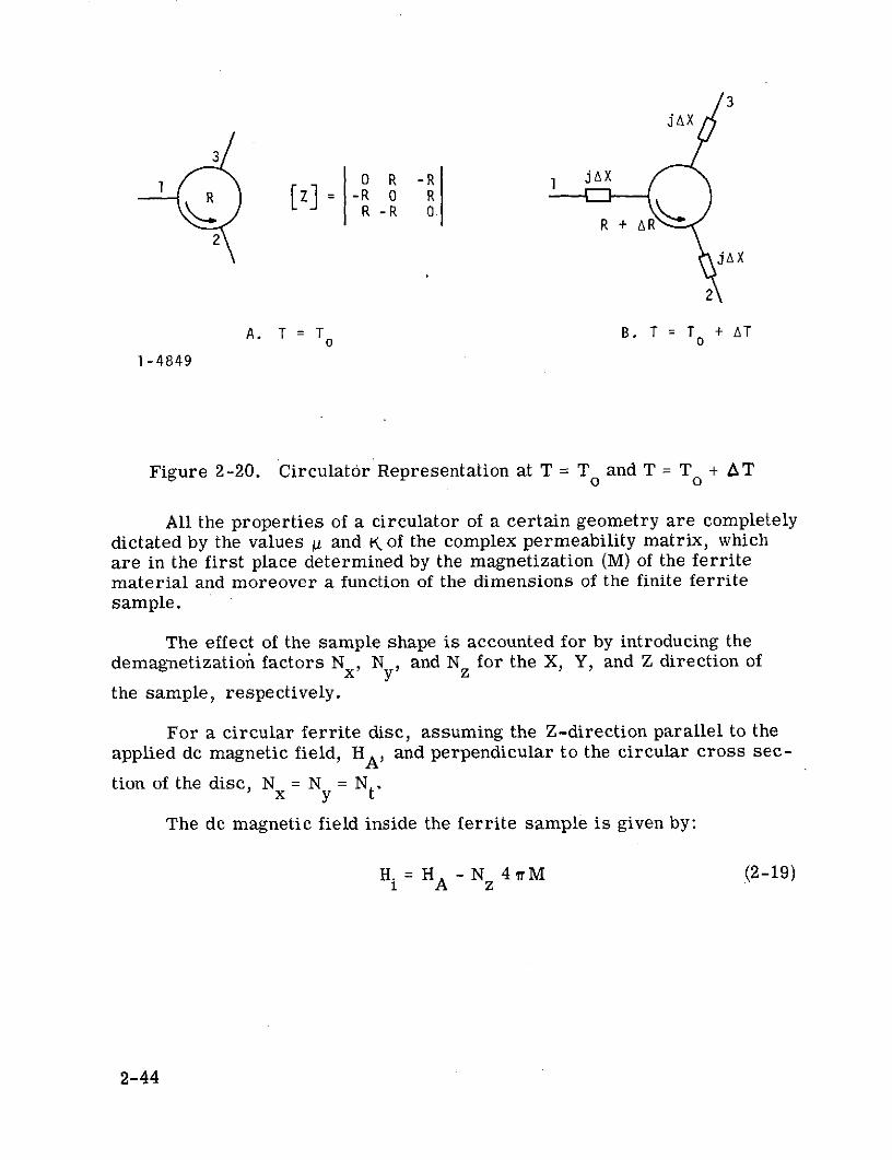
3
1 0 R -R jAXR [Z= -R 0 R
R -R 0R + AR"
jjAX
A. T = T B. T = T + ATo o
1-4849
Figure 2-20. Circulator Representation at T = T and T = T + AT
All the properties of a circulator of a certain geometry are completelydictated by the values L and K, of the complex permeability matrix, whichare in the first place determined by the magnetization (M) of the ferritematerial and moreover a function of the dimensions of the finite ferritesample.
The effect of the sample shape is accounted for by introducing thedemagnetizatiol factors Nx, Ny, and Nz for the X, Y, and Z direction of
the sample, respectively.
For a circular ferrite disc, assuming the Z-direction parallel to theapplied dc magnetic field, HA, and perpendicular to the circular cross sec-
tion of the disc, Nx = N = N t.
The de magnetic field inside the ferrite sample is given by:
H. =H N 4wM (2-19)2-4 A z
2-44
The effective RF resonance field is shown to depend also on the valueof Nt (Kittel) and is given by:
HK = HA + (Nt -Nz) 41M
or (2-20)
H = Hi + Nt 4 M
With these terms defined g and K are given by:
fr Y 41M
=1 + f2 _f 2
r (2-21)
f 4iM
f2 2r
where
fr = VHK
y = gyromagnetic ratio = 2. 8 MHz/oersted
As the circulator characteristics are completely determined by A and )(and assuming HA = constant, it follows that the only way of making the circu-
lator independent of temperature is to keep M constant.
For a circulator biased in the region of magnetic saturation, M = M .s
The saturation magnetization Ms, however, normally varies appre-
ciably with temperature.
Although it is possible to make the magnetic circuit temperature de-pendent, and thus change HA in such a way as to keep one of the parameters,such as HK, constant, thereby changing some of the properties of the circu-
lator less than others, it is impossible to keep the properties constant on allfronts.
2-45
However, there is a solution. From the internal dc magnetic field:
H = HA - N 4r M
therefore, (2-22)
H - H.MA4irM =
Nz
Below saturation M << M s the dc-p of the material is very high. The
result of this is H.i 0, from which 4 1M = HA/NZ so that the value of M is
independent of M s but proportional to HA instead:
M HA for M<<M s
Graphically, this effect is shown in Figure 2-21, where M is given asa function of HA with M s as parameter.
From this graph, it can be seen that, for example at HA 1/2 (4 rMs),M is practically independent of moderate changes of M s
M
MS + AMSM
MS - AMS
NZ 1
27 MS 4 7T MS HA
1-4848
Figure 2-21. Magnetization as Function of de Field and M
2-46
Because in the region H. 0 the Kittel-field HK = Nt 4 1T M is very
small (order of magnitude of Nt = 0. 2) is follows fr << f. Moreover, to
avoid low field losses, the condition of y 4 1 M <f has to be satisfied at alltimes.
Under these conditions, the expressions for U and K go over into
(2-23)
-y 41rMK f
It.can be shown from circulator theory that the frequency determining
parameter is p eff = ( - )/p, whereas the value of R is inversely pro-portional with M.
1
These relations in combination with the above conditions yield:
eff(2-24)
1 -1Ra - aHM A
Thus, for operation below saturation M < Ms, Peff the frequency de-
pendent parameter is independent of temperature as well as of the dc appliedfield so that j AX = 0 (Figure 3-21B). As the expected variation in HA, as a
result of temperature and/or elapsed time, is extremely small in case of theproper choice of magnetic material (for example, Alnico, Cobalt Samarium),the expected AR over the specified temperature range will be far within thelimits allowed by the parametric amplifier as far as the input impedance isconcerned.
However, at first sight, it might be questioned whether this slightchange AR will be small enough not to destroy the critically tuned, high re-turn loss condition of the interjunction that is necessary to make one-passoperation possible.
2-47
Surprisingly, an extra bonus is added in the form of self-regulatingaction of the interjunction, as far as a change in the real value, AR, isconcerned.
As was pointed out, the input impedance, in case of a change of tem-perature or of applied field, is given by:
R + AR + j 6X (2-25)
Under the stated condition of bias field M < M , j AX = 0 so that theinput impedance is R +' R.
This input impedance of the second circulator, however, constitutesthe load impedance of the first circulator which also changed its charac-teristic impedance to R + 4 R, so that, theoretically, a perfect interjunctionmatch is maintained. Even in case slight asymmetries are present, it is,in view of the previous, mechanism, fully justified to render their effectsnegligible.
4. CIRCULATOR MEASURED CHARACTERISTICS
The following are the measured characteristics of the stage 1 and 2prototype circulators and the second-stage output isolator:
a. CIRCULATORS FOR STAGE 1 AND 2
S/N-001 S/N-002
Insertion loss 1-2 (average) 0.10 dB 0. 104 dB
Isolation 2-1 (2. 2 GHz) 38 dB 40 dB
Isolation 2-1 (2. 25 GHz) 40 dB 40 dB
Isolation 2-1 (2. 3 GHz) 43 dB 40 dB
VSWR port 1 1.03 1.07
VSWR port 3 1.03 1.06
Isolation 3-1 (average) 37 dB 32 dB
Insertion loss 2-3 (average) 0.4 0.4 dB
2-48
b. OUTPUT ISOLATION (AVERAGE OVER BAND)
S/N-001
Isolation 2-1 23 dB
Insertion loss 1-2 0. 25 dB
VSWR (input) 1.08
VSWR (output) 1. 06
This indicates that the required high isolation, low forward losstechniques theoretically described in the previous section have been achievedin practice in the S-band system.
2-49
E. PUMP SOURCE
1. GENERAL
The design requirements for the S-band paramp system dictated the
use of a millimeter-wave pump source at an operating frequency of ,-, 50 GHz.
Since a solid-state pump source was specified, the basic choice of oscillator
type was limited to a Gunn-effect device or an IMPATT oscillator. The
main advantage of a Gunn device is that it has a much lower inherent noise
level, while the IMPATT oscillator has the advantage of higher output powerlevels as well as somewhat greater dc-to-RF conversion efficiency. The
pump-power requirements of the amplifier are such that suitable Gunn and
IMPATT devices are both commercially available at the present time.
2. PUMP NOISE CONSIDERATIONS
Since the noise of a pump source can be considered as a random fluctua-tion in instantaneous pump power, the varactor capacitance will fluctuateaccordingly. Because of this, the pump noise is downconverted into thesignal frequency domain, thereby degrading the tangential sensitivity of theamplifier.
In normal operation, even with a noisy pump, this degradation is oftennegligible. However, it has been observed that when a strong interferingsignal is present in close proximity of the received frequency, a severe de-gradation in tangential sensitivity occurred. In this case the pump-derivednoise sidebands of the strong interfering signal increase the input noiselevel at the received frequency. This phenomenon will be explained in somedetail in Appendices C and F, where it will be derived that the degradation in tan-gential sensitivity at f = f as a result of a strong interfering signal Af away,is given by: s
PT(fs f) + K I ps = 1 + F P
PT(f) Top (f) s
where
P = tangential sensitivity at f = fs in the presence
fs ) of an interfering signal 6f away
P = tangential sensitivity at f = f
2-50
K = power gain of amplifier
T = operational temperature T = Tampliier +
signal-sourcew I
-(Af) K figure of merit of pump source
W f) = normalized spectral noise power density of pumposcillator ,f away from carrier
k = Boltzmann's constant = 1.38 x 10- 23 joules/K
P = power of interfering signal 6f away from fsS(A) s
In Figure 2-22, this relation P P is shown graphically as aT(f Af T(fs)
function of Ps(a) with .K/TOp F( f) as parameter.
With the carrier power as 0-reference level, the noise of an oscillatoris often specified by the manufacturer as the decibel-level, seen across asmall bandwidth displaced a given distance from the carrier frequency.From this data, at least one value of W(,) can be obtained.
From reference 2, Figure 2, we derive, as typical numbers for thesepower levels at 100-kHz distance from the carrier in a 100-Hz bandwidth,-128 dB for an IMPATT, and -148 dB for a Gunn effect oscillator. Usingthese numbers we find:
IMPATT: W(1 0 5) = 1.55 x 10 - 1 3 x 10 = 1.55 x 10⁵ (second)
F 5= (10) _ 1.55 x 10- = 1. 12 x 108 (second K)(105) k 1.38 x 10- 23 (joule)
Gunn: W( 1 0 5) = 1.55 x 10
F(10 = 1.12 x 10⁶
2-51
20
107 106 10
15
L T (fSAf) dBT (fS)
10
10
T Op (Af0
103
-60 -50 -40 -30 -20 -10 0
PS (Af) (dBm)
1-4846R1
Figure 2-22. Degradation of Tangential Sensitivity as a Function of
Absolute Power of Interfering Signal
2-52
For an amplifier operational temperature of 100 K and two stages witha gain of 17 dB per stage, it is found that for (K/Top) F(Af) the numbers
are 1.2 x 10⁶ and 1. 12 x 108 for the Gunn and the IMPATT, respectively.
From Figure 2-22, we can derive that the degradation of the tangentialsensitivity will be noticeable when a signal of -60 dBm is present at a dis-tance of 100 kHz when an IMPATT pump source is used.
In the case of a Gunn effect oscillator, the same signal can go up to alevel of -40 dBm before the same degradation is noticed.
The difference of 20 dB in this quite possible range of interfering sig-nal power made AIL decide to choose a Gunn effect oscillator as the pump-power source for the S-band paramp system
3. 50-GHz GUNN OSCILLATOR
A Gunn oscillator was available from Varian Associates which wassuitable for use as a pump source for this program. The pertinent specifi-cations for the type VSQ-9021 Gunn oscillator are:
Frequency 50 GHzPower output (minimum) 75 mW at a flange temperature
of 50 0 CAmplitude variation 0.040 dB/oC (maximum)with temperatureBias voltage 4.0 volts (maximum)Bias current 1.0 ampere (maximum)
Assuming a worst-case total loss of 2. 5 dB for the pump isolator,pump filter, and waveguide sections, a power level of 33.7 mW wouldbe available at the amplifier pump input port. As shown in para-graph II. B. 5, the theoretical pump power required by the amplifier is14. 1 mW which leaves a 3. 8-dB margin in available pump power. Thismargin is sufficient for the system. The final system operated with agood margin of pump power.
The basic unstabilized oscillator has an amplitude stability of0. 040 dB/oC by temperature stabilizing the GDO's at 50 10oC.
An isolator is necessary at the output of the Gunn oscillator to ensureamplitude and frequency stability of the Gunn source. A suitable 50-GHzisolator having a maximum insertion loss of 0. 5 dB and a minimum isolationloss of 20 dB was developed by AIL and is employed in this system.
2-53
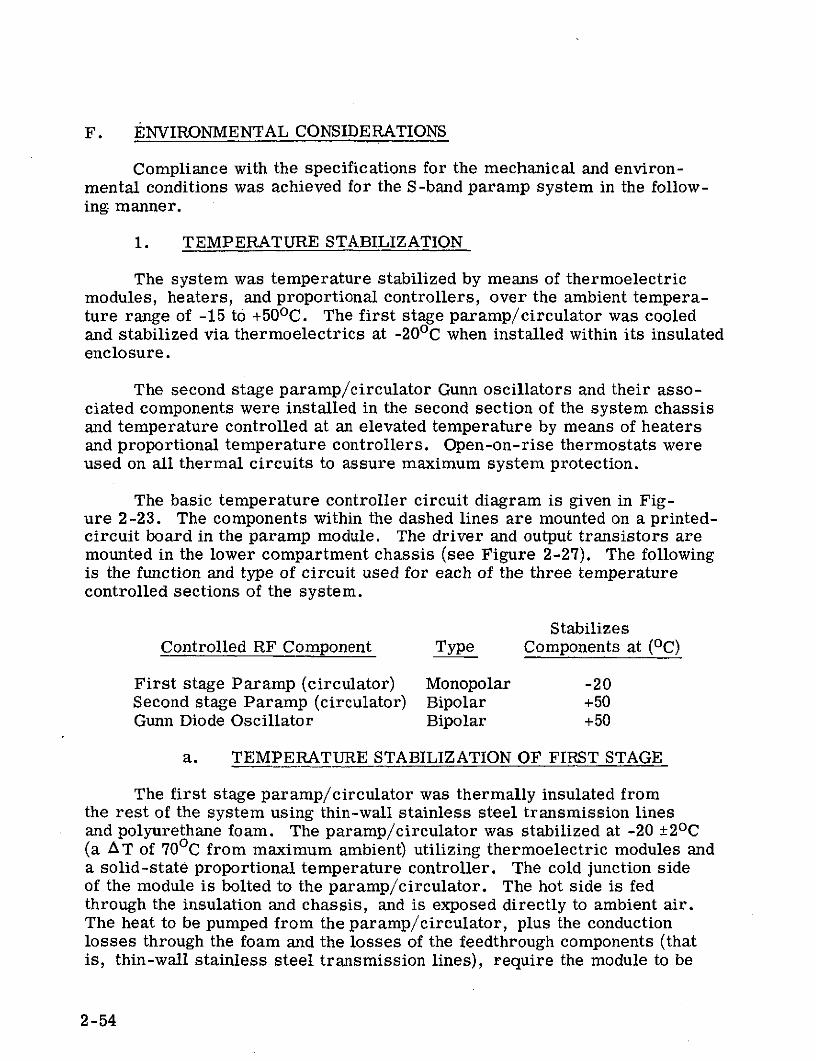
F. ENVIRONMENTAL CONSIDERATIONS
Compliance with the specifications for the mechanical and environ-mental conditions was achieved for the S-band paramp system in the follow-ing manner.
1. TEMPERATURE STABILIZATION
The system was temperature stabilized by means of thermoelectricmodules, heaters, and proportional controllers, over the ambient tempera-ture range of -15 to +50 0 C. The first stage paramp/circulator was cooledand stabilized via thermoelectrics at -20 0 C when installed within its insulatedenclosure.
The second stage paramp/circulator Gunn oscillators and their asso-ciated components were installed in the second section of the system chassisand temperature controlled at an elevated temperature by means of heatersand proportional temperature controllers. Open-on-rise thermostats wereused on all thermal circuits to assure maximum system protection.
The basic temperature controller circuit diagram is given in Fig-ure 2-23. The components within the dashed lines are mounted on a printed-circuit board in the paramp module. The driver and output transistors aremounted in the lower compartment chassis (see Figure 2-27). The followingis the function and type of circuit used for each of the three temperaturecontrolled sections of the system.
StabilizesControlled RF Component Type Components at (oC)
First stage Paramp (circulator) Monopolar -20Second stage Paramp (circulator) Bipolar +50Gunn Diode Oscillator Bipolar +50
a. TEMPERATURE STABILIZATION OF FIRST STAGE
The first stage paramp/circulator was thermally insulated fromthe rest of the system using thin-wall stainless steel transmission linesand polyurethane foam. The paramp/circulator was stabilized at -20 +20 C(a AT of 70 0 C from maximum ambient) utilizing thermoelectric modules anda solid-state proportional temperature controller. The cold junction sideof the module is bolted to the paramp/circulator. The hot side is fedthrough the insulation and chassis, and is exposed directly to ambient air.The heat to be pumped from the paramp/circulator, plus the conductionlosses through the foam and the losses of the feedthrough components (thatis, thin-wall stainless steel transmission lines), require the module to be
2-54
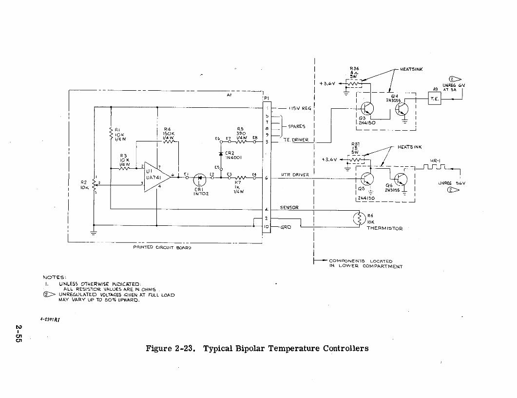
R36 HEATSINKAlp
+I5v RE;Al Q A4A9P 2N3055
7 S E N4150
RI R4 R5 8 SPARESIO K 150K 390 1/4W /4 EG E7 1/4W E8 TE. DRIVER R37
15 HEATSNK
W IN4001 +
V4IN 2 7 E5I t -
UA71 6R2 2 3 L RTR DRIVERUNRE 5
I UNL K CRI 5 2N3055N ,1/4LL 3O VIN OV
PRINTED CIRCUIT BOARD
IN LOWER COMPARTMENT
NOT ES
ALL RESISTOR VALUES ARE IK OHMS1Z ' UNRECGULATED VOLTAES QIVEN AT FULL LOAD
MAY VARY UP TO 50% UP~WARD.
4 -2591R1
Figure 2-23. Typical Bipolar Temperature Controllers
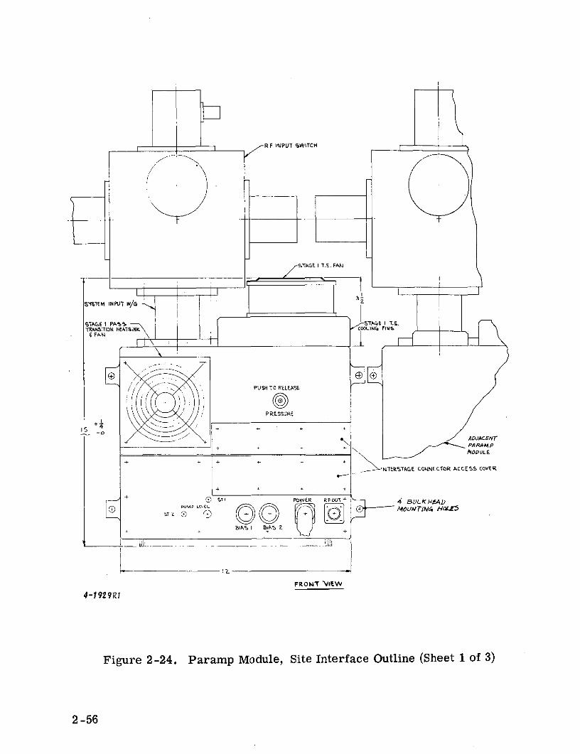
V 1 RF INPUT SWITCH
-tS TEM INPUT W/Gj
STAGE i PASSA I .E.TRANSITION HeAMslK COON FINS
(FA
4
PUSH TO RELEASE
PRLSSURE
ADJACENr+ tPARA M P
-NTRSTAGE CO~N ECTOR ACCESS COVER
0 ST POWER RFOUT 4 BULKMEADSPUMP C L OAITI HoCLLE
I BIAS I WA5 Z
FRONT 'VIEW
4-1929R1
Figure 2-24. Paramp Module, Site Interface Outline (Sheet 1 of 3)
2-56
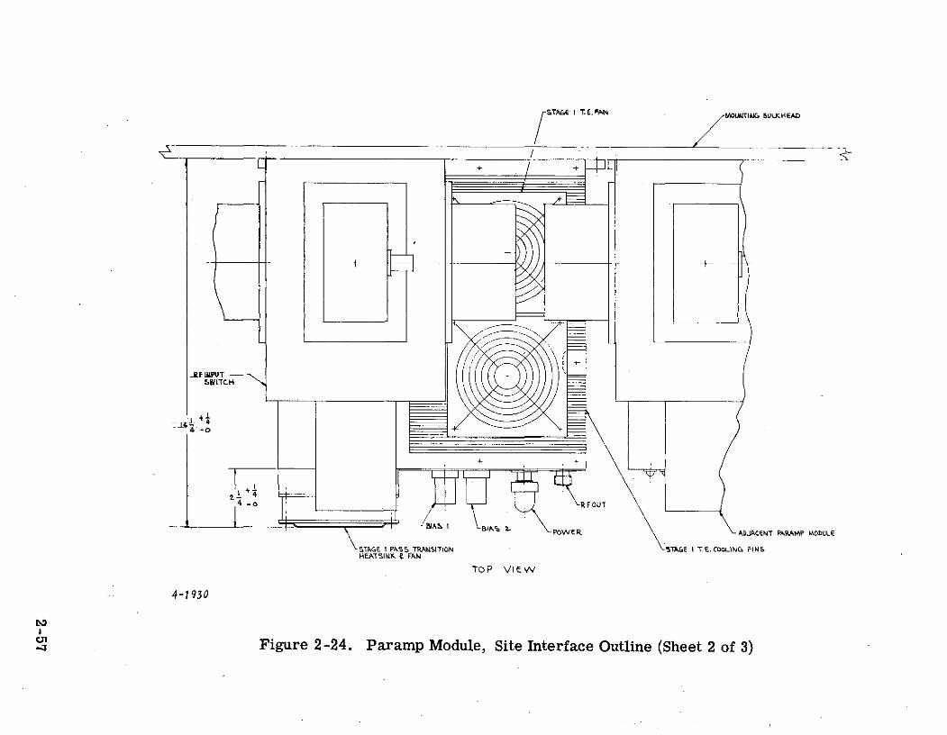
STAGE I TE. FAN MOUNTIG BULKHEAD
++ +
-4,-0A-"
0 \RFOUT
0-7-
IA1 I BIN% 7 POWePR AbJACENT PARAMP MODULE
STAGE I PASS TRANSITION STAGE I T.E.COOLING FINSHEATSIMKK t FAN
TOP VI.Wt
4-1930
Figure 2-24. Paramp Module, Site Interface Outline (Sheet 2 of 3)
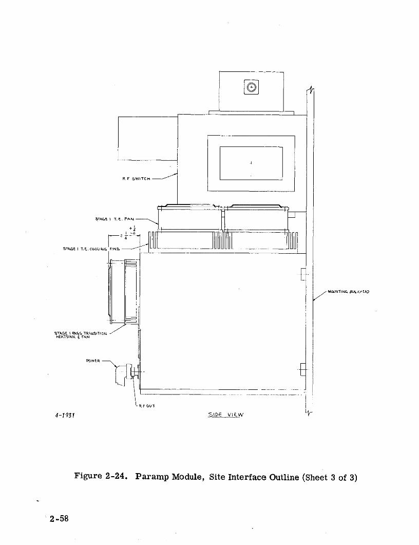
R F SWITCH
S7AZ.t I T. E FAM
S-o
S2-
STAGE I T.E. COOLIMG FINS - _
MOUNtINC4 8ULKH~A
STAGE I PASS TRPMSIToFWHEATS NK , FAN
POWER
RF ouT
4-1931 SIDE VEW
Figure 2-24. Paramp Module, Site Interface Outline (Sheet 3 of 3)
2-58
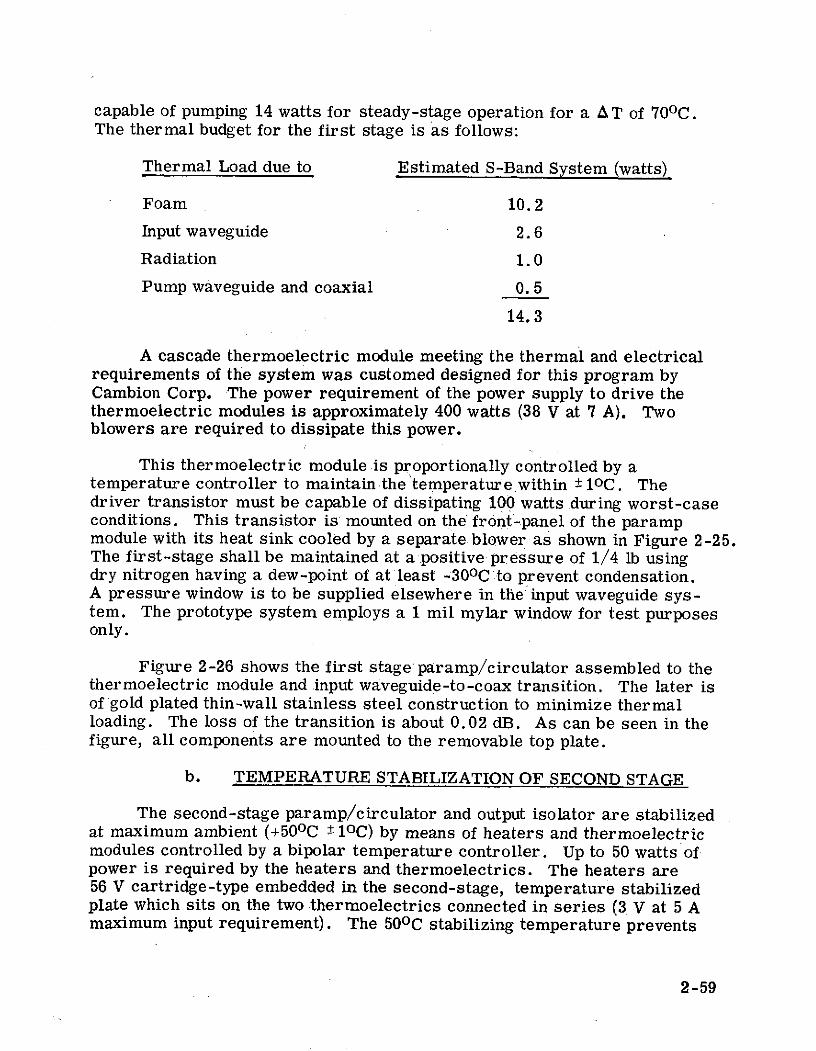
capable of pumping 14 watts for steady-stage operation for a AT of 70 0 C.The thermal budget for the first stage is as follows:
Thermal Load due to Estimated S-Band System (watts)
Foam 10.2
Input waveguide 2.6
Radiation 1.0
Pump waveguide and coaxial 0. 5
14.3
A cascade thermoelectric module meeting the thermal and electricalrequirements of the system was customed designed for this program byCambion Corp. The power requirement of the power supply to drive thethermoelectric modules is approximately 400 watts (38 V at 7 A). Twoblowers are required to dissipate this power.
This thermoelectric module is proportionally controlled by atemperature controller to maintain the temperature within t loC. Thedriver transistor must be capable of dissipating 100 watts during worst-caseconditions. This transistor is mounted on the front-panel of the parampmodule with its heat sink cooled by a separate blower as shown in Figure 2-25.The first-stage shall be maintained at a positive pressure of 1/4 lb usingdry nitrogen having a dew-point of at least -30 0 C to prevent condensation.A pressure window is to be supplied elsewhere in the input waveguide sys-tem. The prototype system employs a 1 mil mylar window for test purposesonly.
Figure 2-26 shows the first stage paramp/circulator assembled to thethermoelectric module and input waveguide-to-coax transition. The later isof gold plated thin-wall stainless steel construction to minimize thermalloading. The loss of the transition is about 0.02 dB. As can be seen in thefigure, all components are mounted to the removable top plate.
b. TEMPERATURE STABILIZATION OF SECOND STAGE
The second-stage paramp/circulator and output isolator are stabilizedat maximum ambient (+50 0 C ± loC) by means of heaters and thermoelectricmodules controlled by a bipolar temperature controller. Up to 50 watts ofpower is required by the heaters and thermoelectrics. The heaters are56 V cartridge-type embedded in the second-stage, temperature stabilizedplate which sits on the two thermoelectrics connected in series (3 V at 5 Amaximum input requirement). The 50 0 C stabilizing temperature prevents
2-59
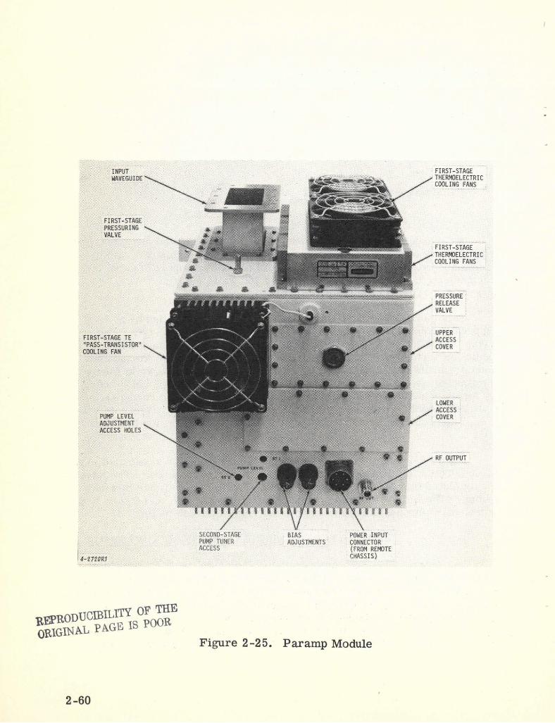
WAVEGUIDE . THERMOELECTRIC, NCOOLING FANS
FIRST-STAGEPRESSURINGVALVE
FIRST-STAGETHERMOELECTRICCOOLING FANS
AL
PRESSURERELEASEVALVE
FIRST-STAGE TE ACCESS"PASS-TRANSISTOR' COVERCOOLING FAN
7 LOWERACCESS
PUMP LEVEL COVERADJUSTMENTACCESS HOLES
RF OUTPUT
SECOND-STAGE BIAS POWER INPUTPUMP TUNER ADJUSTMENTS CONNECTORACCESS (FROM REMOTE
4-2720R1 CHASSIS)
yEPRoDUCIBILITY OF TILEoRIGINAL PAGE IS pOO
Figure 2-25. Paramp Module
2-60
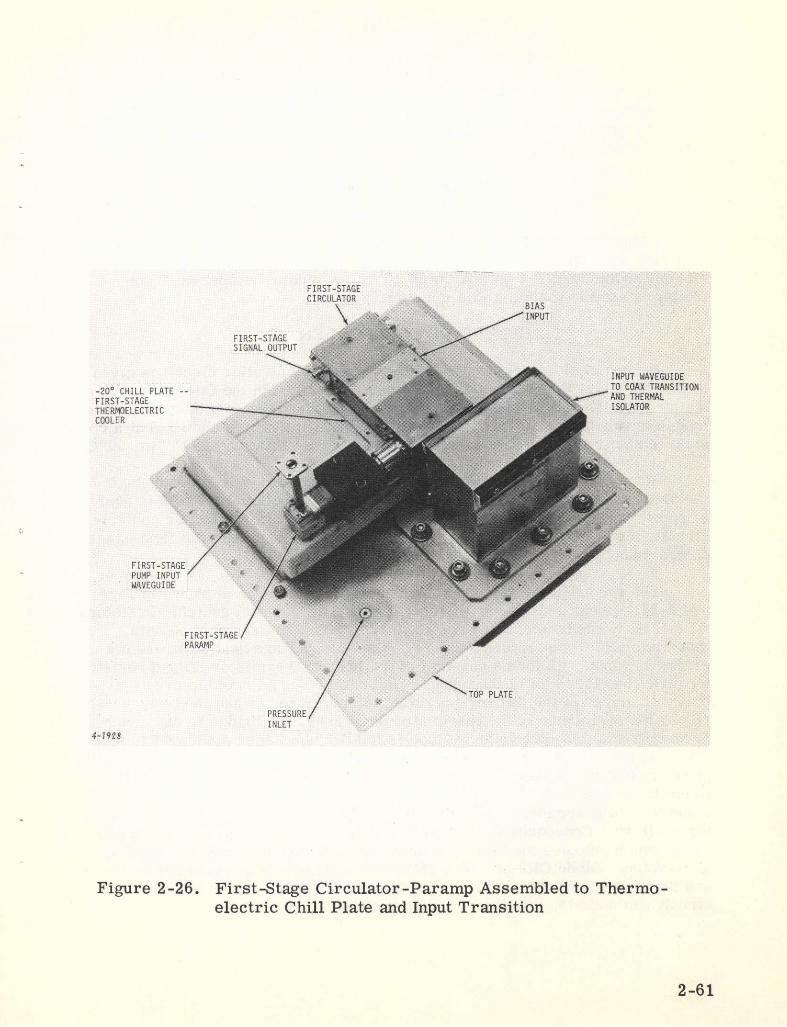
FIRST-STAGECIRCULATOR
BIASINPUT
FIRST-STAGESIGNAL OUTPUT
INPUT WAVEGUIDE
-20 CHILL PLATE -- TO COAX TRANSITION
FIRST-STAGE ISOLATORMA
THERMOELECTRIC ISOLATOR
COOLER
FIRST-STAGEPUMP INPUTWAVEGUIDE
FIRST-STAGEPARAMP
TOP PLATE
PRESSUREINLET
4-1928
Figure 2-26. First-Stage Circulator-Paramp Assembled to Thermo-electric Chill Plate and Input Transition
2-61
condensation since it is equal or higher than maximum ambient. Theprototype design does, however, allow for pressurization of the lower com-partment for use in areas of very severe environmental conditions (humidity,dust, and so on).
c. TEMPERATURE STABILIZATION OF GUNNOSCILLATORS
Both first and second stage Gunn oscillators are mounted on a commonheat sink and stabilized by means of a cartridge heater and two thermo-electric modules (2.6 V at 5 A) at 50 ± 10 C. A bipolar temperature con-troller is used to maintain this temperature.
d. TEMPERATURE CONTROLLER
A functional description of the temperature controller circuit is givenin this section. Exact details of the circuit are given in the Operations andMaintenance Manual. This circuit controls the de power to a thermoelectricmodule and heater element to maintain the amplifier stages and GDO at a con-stant temperature over the baseplate temperature variation of -150 to +50 0 C.
Since the operation of these circuits are similar, only second-stagetemperature controller Al is described. The monopolar circuit A2 is equiva-lent, with the exception that it does not include or require a heater control-circuit, since this is provided by the normal "heat-leak" into the first-stagecompartment.
The second-stage temperature controller schematic is shown in Fig-ure 2-23. Integrated circuit U1 functions as a differential switch. ResistorsR1 and R2 in the temperature control circuit board, in conjunction withthermistor R6 (temperature sensor) on the second stage heat sink, form abridge network. R2 forms one-half of the bridge; thermistor R6 and resistorR1 form the other half of the bridge. Resistor R2 is adjusted to create abalanced bridge at the desired operating temperature. When the temperaturerises, the resistance of the thermistor decreases, the bridge is unbalanced,producing a high output voltage which is fed through Zener diodes CR1, andR5 to Q3 and Q4, the '"Darlington" connected driver transistors, which supplypower to the thermoelectric module (A9). When the circuit is cooled suf-ficiently, the thermistor resistance increases giving reduced output from1 and 0 volts at terminal "E2" (due to the drop through Zener CR1). Thisturns off Q5. Consequently, the collector of Q3 is at high potential, turningon Q6 which actuates the heater to drive the temperature back up to the set-point value. Diode CR2 provides an "offset voltage" to separate the heaterand thermoelectric turn-on points to prevent "hunting. " This controllercircuit can maintain the setpoint temperature to within 0. 50 C.
2-62
Although initial thermal tests of these circuits indicated that proportionalcontrol was maintained at all points in the -15 to +500C temperature range,final system tests show additional heater capacity is required in the GDOstability circuit. A larger heater would be used in the production units.
2. ENVIRONMENT CONSIDERATIONS (SHOCK AND VIBRATION)
The parametric amplifier system has been designed to operate satis-factorily within the dynamic environmental specification as encountered intypical ground base antenna system employing a hydraulic drive system.
Typical specifications for this type of system are vibration levels upto 2 g from 30 to 500 Hz, 0.05-inch maximum double amplitude displace-ment from 1.5 to 30 Hz.
Based upon previous experience with the vibration characteristicsassociated with ground-based antennas, no problem was expected in thedynamic environment as related to this system. The basic design approachfor the structural and dynamic environment was to limit the amplitude ofmotion of the common baseplate below 500 Hz therby isolating the systemcomponents from the dynamic environment.
G. PACKAGING REQUIREMENTS
The type A-471 prototype system has been packaged to meet the siteinterface requirements required for this program as follows.
1. PARAMP MODULE
The module has been designed to be installed against a bulkhead bymeans of four mounting tabs. Access for all tuning adjustment is from thefront-only as required in a 26-meter antenna site where two units are mountedside by side and other components are installed on either side of these.These limitations have required careful layout and design to properly locateall components in the allotted space. Figure 2-24 is an outline drawing of theA-471 system connected to the 26-meter antenna site input RF switch. Sitesusing the 9-meter antennas have less stringent mounting requirements sincethe paramp module will be mounted in a standard rack enclosure.
2-63
The module is divided into an upper area which is pressurized andcontains the first-stage paramp/circulator mounted on the thermoelectriccooler. These components are all mounted to the top plate which isgasketed to maintain a low leakage rate. After fastening the top plate tothe module housing the connections to the second-stage, bias and powerconnections are made by removing the upper gasketed access cover whichcontains an overpressure relief and release valve.
The lower compartment components are mounted on a heat-sink whichcan be slid out of the housing after removing the front-panel screws and dis-connecting the connections to the first stage. The latter are exposed byremoving the lower access cover. The design of the lower compartment issuch as to make it adaptable to pressurization as may be required at somesites. The following components are located in the lower compartment:
* First and second stage Gunn diode oscillators,isolators, test couplers and pump level set attenuators
* Second stage paramp/circulator
* Paramp and Gunn diode bias adjustment potentiometers
* Temperature controller boards
* Integrated regulator modules for paramp bias and GDObias
Pass transistors for all temperature stabilizingelement except first stage thermoelectric module
* Bias divider and monitoring boards
* Output filter
Figure 2-27 shows the layout of the drawer in the prototype unit.The various components listed are identified in this figure. The detailedschematic diagrams are given in the Operations and Maintenance Manualfor this program.
In the production units all terminal boards will be replaced withprinted-circuit boards for ease of assembly and compactness. Terminalboards were used in some circuits of the prototype to facilitate design ad-justments and testing. The paramp module with both access covers in-stalled is shown in Figure 2-25.
The pump level and bias adjustment seen in this figure would beplaced under a separate access cover in the proposed production units tomeet EMI requirements. In addition, an EMI filter box would be incor-porated at the power connector.
2-64
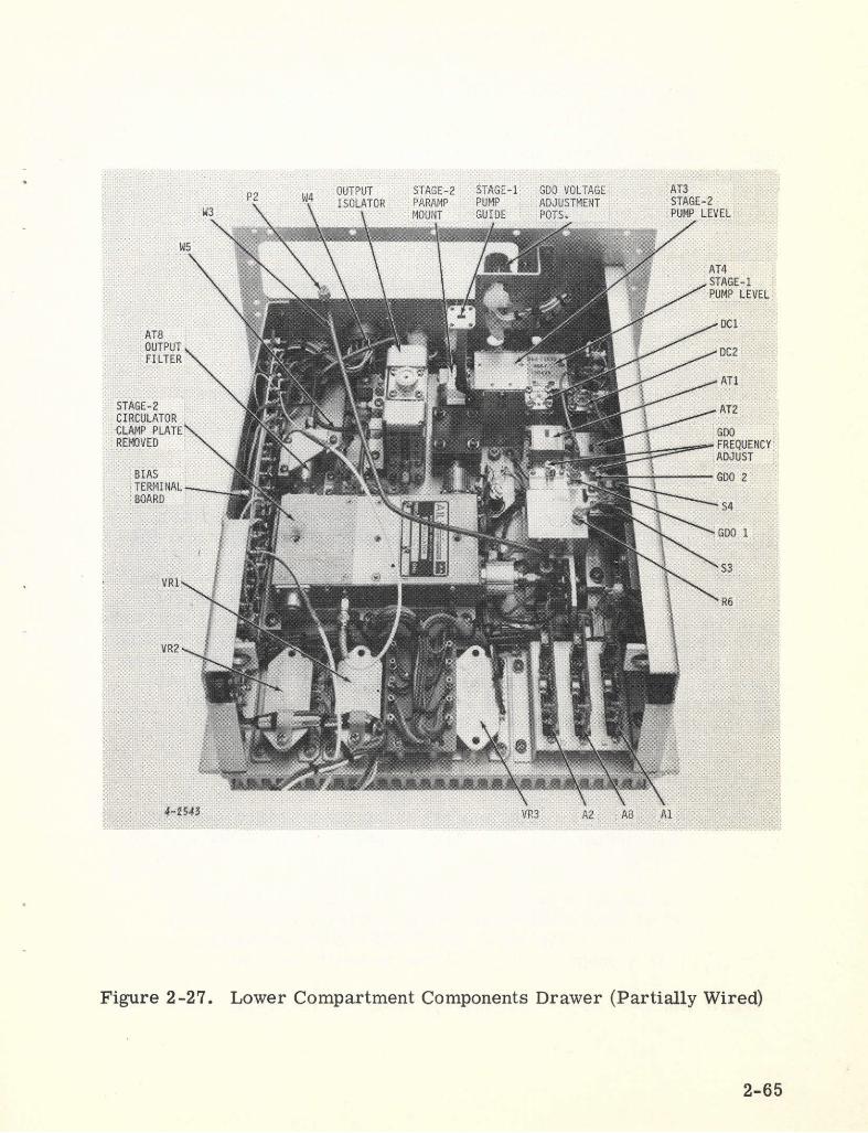
OUTPUT STAGE-2 STAGE-1 GDO VOLTAGE AT3SISOLATOR PARAMP PUMP ADJUSTMENT STAGE-2
W3 MOUNT GUIDE POTS. PUMP LEVEL
W5
W" AT4SSTAGE-1
SPUMP LEVEL
DCCIRCULATAT8OUTPUTFILTER"
AT1
STAGE-2 AT2CIRCULATORCLAMP PLATE GDOREMOVED FREQUENCY
ADJUST
BIAS GDO 2TERMINALBOARD S4
GDO 1
VR2
4-2543 VR3 A2 A8 Al
Figure 2-27. Lower Compartment Components Drawer (Partially Wired)
2-65
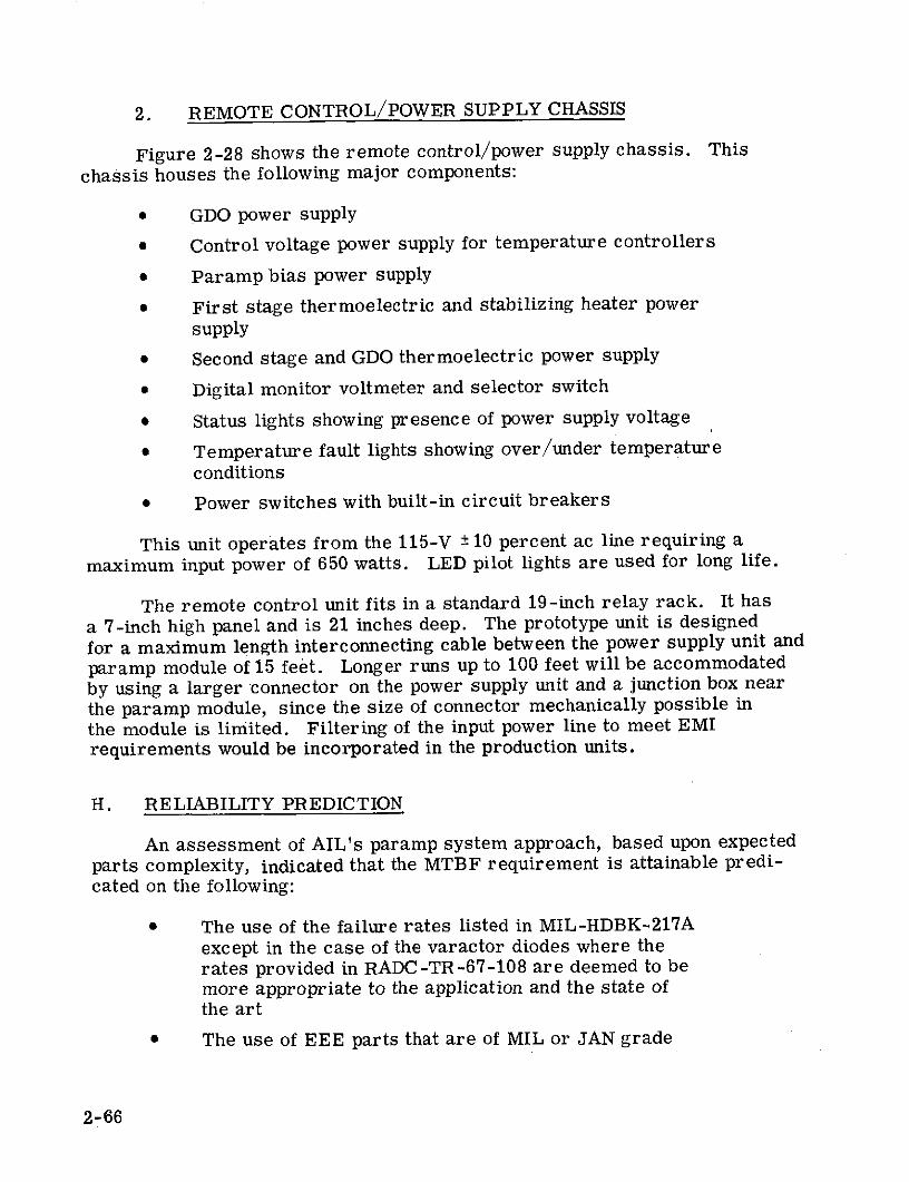
2. REMOTE CONTROL/POWER SUPPLY CHASSIS
Figure 2-28 shows the remote control/power supply chassis. This
chassis houses the following major components:
* GDO power supply
* Control voltage power supply for temperature controllers
* Paramp bias power supply
* First stage thermoelectric and stabilizing heater power
supply
* Second stage and GDO thermoelectric power supply
* Digital monitor voltmeter and selector switch
* Status lights showing presence of power supply voltage
* Temperature fault lights showing over/under temperature
conditions
* Power switches with built-in circuit breakers
This unit operates from the 115-V ± 10 percent ac line requiring amaximum input power of 650 watts. LED pilot lights are used for long life.
The remote control unit fits in a standard 19-inch relay rack. It has
a 7-inch high panel and is 21 inches deep. The prototype unit is designedfor a maximum length interconnecting cable between the power supply unit and
paramp module of 15 feet. Longer runs up to 100 feet will be accommodated
by using a larger connector on the power supply unit and a junction box near
the paramp module, since the size of connector mechanically possible in
the module is limited. Filtering of the input power line to meet EMI
requirements would be incorporated in the production units.
H. RELIABILITY PREDICTION
An assessment of AIL's paramp system approach, based upon expected
parts complexity, indicated that the MTBF requirement is attainable predi-cated on the following:
* The use of the failure rates listed in MIL-HDBK-217Aexcept in the case of the varactor diodes where therates provided in RADC-TR-67-108 are deemed to bemore appropriate to the application and the state ofthe art
* The use of EEE parts that are of MIL or JAN grade
2-66
4-1934
Figure 2-28. Remote Control/Power Supply Chassis
2-67
Note
The use of EEE parts of established reliability grade(ER or JANTX) would yield a predicted increase inMTBF by a factor of approximately 1.17.
Derating of EEE parts to approximately 25 percent ofmanufacturer's ratings at an average ambient parttemperature of approximately 600C
A summary of the failure rate estimates for various units of theS-band paramp system (single varactor diode configuration) is given inTable 2-4. These estimates yield the following values of predicted MTBF:
Total Failure MTBFRate (fpMh) (hours)
55.51 18, 015
This exceeds the minimum 10, 000 hours required in the contract.
2-68
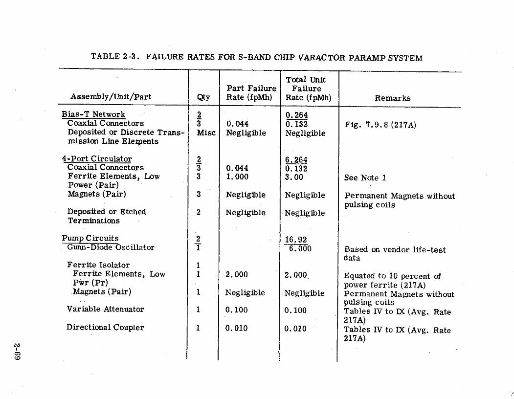
TABLE 2-3. FAILURE RATES FOR S-BAND CHIP VARACTOR PARAMP SYSTEM
Total UnitPart Failure Failure
Assembly/Unit/Part Qty Rate (fpMh) Rate (fpMh) Remarks
Bias-T Network 2 0.264Coaxial Connectors 3 0.044 0.132 Fig. 7.9.8 (217A)Deposited or Discrete Trans- Misc Negligible Negligiblemission Line Elerpents
4-Port Circulator 2 6. 264Coaxial Connectors 3 0.044 0.132Ferrite Elements, Low 3 1.000 3.00 See Note 1Power (Pair)Magnets (Pair) 3 Negligible Negligible Permanent Magnets without
pulsing coilsDeposited or Etched 2 Negligible NegligibleTerminations
Pump Circuits 2 16.92Gunn-Diode Oscillator - 6.000 Based on vendor life-test
dataFerrite Isolator 1
Ferrite Elements, Low 1 2.000 2. 000 Equated to 10 percent ofPwr (Pr) power ferrite (217A)Magnets (Pair) 1 Negligible Negligible Permanent Magnets without
pulsing coilsVariable Attenuator 1 0. 100 0. 100 Tables IV to IX (Avg. Rate
217A)Directional Coupler 1 0. 010 0.010 Tables IV to IX (Avg. Rate
217A)0~3
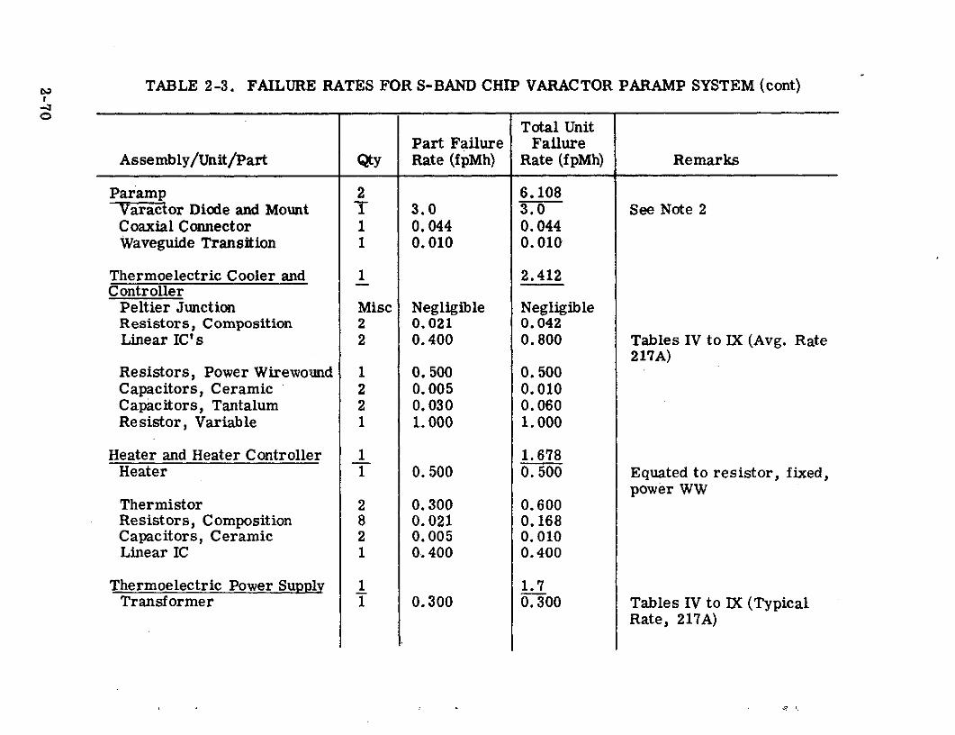
TABLE 2-3. FAILURE RATES FOR S-BAND CHIP VARACTOR PARAMP SYSTEM (cont)
Total UnitPart Failure Failure
Assembly/Unit/Part Qty Rate (fpMh) Rate (fpMh) Remarks
Paramp 2 6.108Varactor Diode and Mount T 3.0 3.0 See Note 2Coaxial Connector 1 0.044 0.044Waveguide Transition 1 0.010 0.010
Thermoelectric Cooler and 1 2.412Controller
Peltier Junction Misc Negligible NegligibleResistors, Composition 2 0.021 0.042Linear IC's 2 0.400 0.800 Tables IV to IX (Avg. Rate
217A)Resistors, Power Wirewound 1 0. 500 0.500Capacitors, Ceramic 2 0.005 0.010Capacitors, Tantalum 2 0.030 0.060Resistor, Variable 1 1. 000 1. 000
Heater and Heater Controller 1 1.678Heater 1 0. 500 0. 500 Equated to resistor, fixed,
power WWThermistor 2 0.300 0.600Resistors, Composition 8 0. 021 0.168Capacitors, Ceramic 2 0.005 0.010Linear IC 1 0.400 0.400
Thermoelectric Power Supply 1 1.7Transformer 1 0.300 0.300 Tables IV to IX (Typical
Rate, 217A)
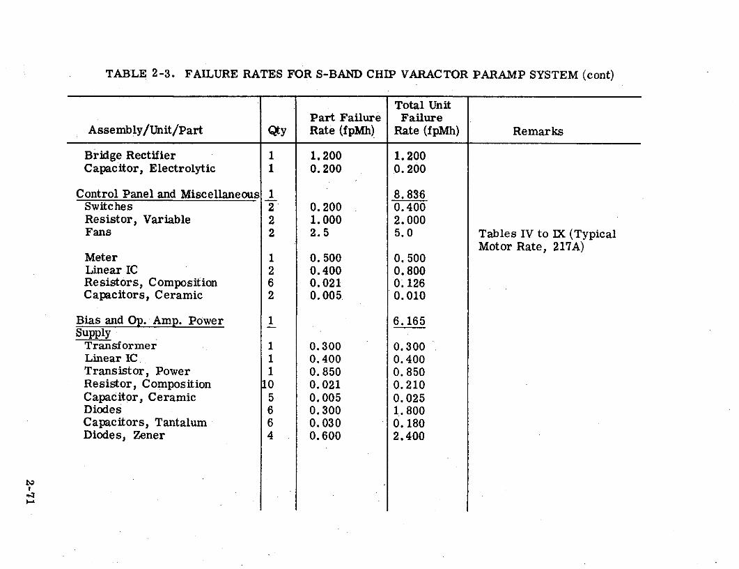
TABLE 2-3. FAILURE RATES FOR S-BAND CHIP VARACTOR PARAMP SYSTEM (cont)
Total UnitPart Failure Failure
Assembly/Unit/Part Qty Rate (fpMh) Rate (fpMh) Remarks
Bridge Rectifier 1 1.200 1. 200Capacitor, Electrolytic 1 0.200 0. 200
Control Panel and Miscellaneous 1 8. 836Switches 2 0.200 0.400Resistor, Variable 2 1.000 2.000Fans 2 2.5 5.0 Tables IV to IX (Typical
Motor Rate, 217A)Meter 1 0. 500 0. 500Linear IC 2 0. 400 0. 800Resistors, Composition 6 0.021 0.126Capacitors, Ceramic 2 0.005 0.010
Bias and Op. Amp. Power 1 6.165Supply
Transformer 1 0.300 0.300Linear IC 1 0.400 0.400Transistor, Power 1 0.850 0. 850Resistor, Composition 10 0.021 0.210Capacitor, Ceramic 5 0.005 0.025Diodes 6 0.300 1.800Capacitors, Tantalum 6 0.030 0.180Diodes, Zener 4 0.600 2.400
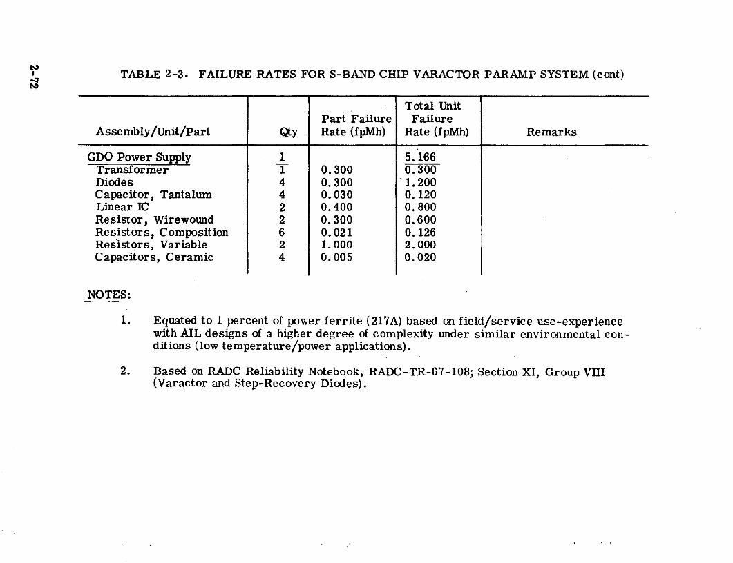
TABLE 2-3. FAILURE RATES FOR S-BAND CHIP VARACTOR PARAMP SYSTEM (cont)
Total UnitPart Failure Failure
Assembly/Unit/Part Qty Rate (fpMh) Rate (fpMh) Remarks
GDO Power Supply 1 5. 166Transformer 1 0.300 0.300Diodes 4 0.300 1.200Capacitor, Tantalum 4 0.030 0.120Linear IC 2 0.400 0.800Resistor, Wirewound 2 0.300 0.600Resistors, Composition 6 0.021 0.126Resistors, Variable 2 1. 000 2. 000Capacitors, Ceramic 4 0.005 0.020
NOTES:
1. Equated to 1 percent of power ferrite (217A) based on field/service use-experiencewith AIL designs of a higher degree of complexity under similar environmental con-ditions (low temperature/power applications).
2. Based on RADC Reliability Notebook, RADC-TR-67-108; Section XI, Group VIII(Varactor and Step-Recovery Diodes).
A. GENERAL
The RF components of the system were assembled about midway throughthe program (February 1974) to evaluate performance with a room tempera-ture first stage. The results of these tests are given in Section A. The re-sults of the tests on the final packaged system, with the first stage cooled to-20 0 C are presented in Section B.
B. BREADBOARD SYSTEM
The Model A471 breadboard system microwave components were as-sembled and measured as a two-stage room temperature system during theFebruary 1974 review.meeting on the prototype development program. Thetests were monitored by the NASA technical officer on this program. Thesummary of the measured performance is given in Table 3-1.
TABLE 3-1. MEASURED PERFORMANCE SUMMARY OF S-BANDPARAMP MOUNT SYSTEM (ROOM TEMPERATURE STAGE 1)
Data Taken: February 14, 1974
A. System Performance
Center Frequency: 2265 MHz
Bandwidth (1 dB down): 145 MHz
1 dB Down Frequencies: 2185 and 2330 MHz
Gain (Port to Port): 31 dB
Input VSWR (Maximum 1.3Operating Over Band):
Compression Level (1 dB -47 dBmDown):
3-1
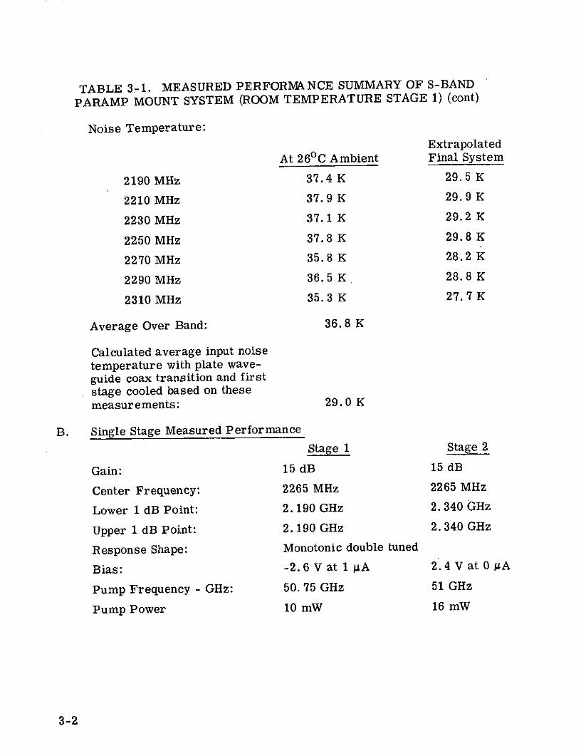
TABLE 3-1. MEASURED PERFORMANCE SUMMARY OF S-BAND
PARAMP MOUNT SYSTEM (ROOM TEMPERATURE STAGE 1) (cont)
Noise Temperature:Extrapolated
At 26 0 C Ambient Final System
2190 MHz 37.4 K 29.5 K
2210 MHz 37.9 K 29.9 K
2230 MHz 37.1 K 29.2 K
2250 MHz 37.8 K 29.8 K
2270 MHz 35.8 K 28.2 K
2290 MHz 36.5 K 28.8 K
2310 MHz 35.3 K 27. 7 K
Average Over Band: 36.8 K
Calculated average input noisetemperature with plate wave-guide coax transition and firststage cooled based on thesemeasurements: 29.0 K
B. Single Stage Measured Performance
Stage 1 Stage 2
Gain: 15 dB 15 dB
Center Frequency: 2265 MHz 2265 MHz
Lower 1 dB Point: 2. 190 GHz 2. 340 GHz
Upper 1 dB Point: 2. 190 GHz 2. 340 GHz
Response Shape: Monotonic double tuned
Bias: -2.6 V at 1 A 2.4 V at 0 IA
Pump Frequency - GHz: 50. 75 GHz 51 GHz
Pump Power 10 mW 16 mW
3-2
Figure 3-1A shows the two-stage pass-band taken during the Februaryreview meeting demonstration. The 136-MHz, 1-dB down bandwidth morethan meets the 100-MHz, 1-dB down, minimum bandwidth requirement. Thenoise temperature data measured during the review meeting is given inTable 3-1 and is plotted in Figure 3-1B. The average noise temperature is36. 8 K for seven frequencies measured across the band. The equivalentaverage final system noise temperature was calculated to be 29 K based on afirst stage stabilized at -20 0 C and a second stage stabilized at +50 0 C. Thisis less than the 30 K maximum noise temperature specification. This hasbeen borne out by subsequent measurements on the final system. Since to-date the prototype system has not been fully tested in the final cooled con-figuration, the 30 K noise temperature can only be taken as a design goalwith 35 K as a firm specification. This is because changes in cooled circu-lator characteristics, and an additional length of input waveguide to matewith the input RF switch may slightly increase the input noise temperature.
The first stage circulator was adjusted for optimum performance at-20 0 C. Performance at room temperature will be possible by readjustmentof the pump and bias levels of the paramp and GDO in case of failure of thefirst-stage thermoelectric module. Operation would be normal except theinput noise temperature would increase about 6 K.
Figure 3-1C shows the measured active and inactive input VSWR acrossthe band. This is less than the 1. 5 to 1 required VSWR. Figure 3-2 givesthe amplifier saturation characteristic. The measured 1-dB compressionpoint is -47.4 dBm which is below the -50 dBm required. A photograph ofthe two-stage system RF components assembled for this test are shown inFigure 3-3.
C. MEASURED PERFORMANCE - PROTOTYPE SYSTEM
Final acceptance tests of the complete prototype system were performedat AIL during October and November 1974 using NASA approved "AcceptanceTest Procedure" No. 376807. The tests were monitored by the NASA tech-nical officer, DCAS, and Quality Assurance at AIL. Results of the tests ascompared with the specifications are given in Table 3-2. As can be seen, thesystem met or exceeded all the electrical performance requirements. Theonly exception was that the gain variation with change in ambient temperatureslightly exceeded specifications below 100 C. This problem can be readilysolved in production units by using higher-power heater elements in the GDOand second-stage stabilizing circuits. The following figures show the majormeasured performance characteristics as plotted from the test data.
3-3
Figure No. Parameters Plotted
3-4 Gain-Bandwidth Characteristics
3-5 Noise Temperature Versus Frequency
3-6 Input-Output VSWR Versus Frequency
3-7 Dynamic Range Versus Frequency
3-8 Phase Linearity Versus Frequency
3-9 Envelope Delay Distortion Versus Frequency
3-10 Gain Stability Versus Thermal Cycling
The plots are basically self-explanatory. It should be noted that thevariation in the phase linearity versus frequency plot (Figure 3-8) near mid-band is possibly attributable to the waveguide-to-coax transition and coaxialbends since it also appears in the reference phase plot.
The level of pump frequency spurious output (Table 3-2) will meetspecifications even though the specified level is below the range of sensitivityof available test equipment. This is based on the fact that the output filterhas a pump-frequency rejection of better than 80 dB and the amplifier/circu-lator normally have rejection levels of 35 dB, giving a total rejection ofgreater than 115 dB. This is above the 100-dB minimum rejection requiredin the specifications.
3-4
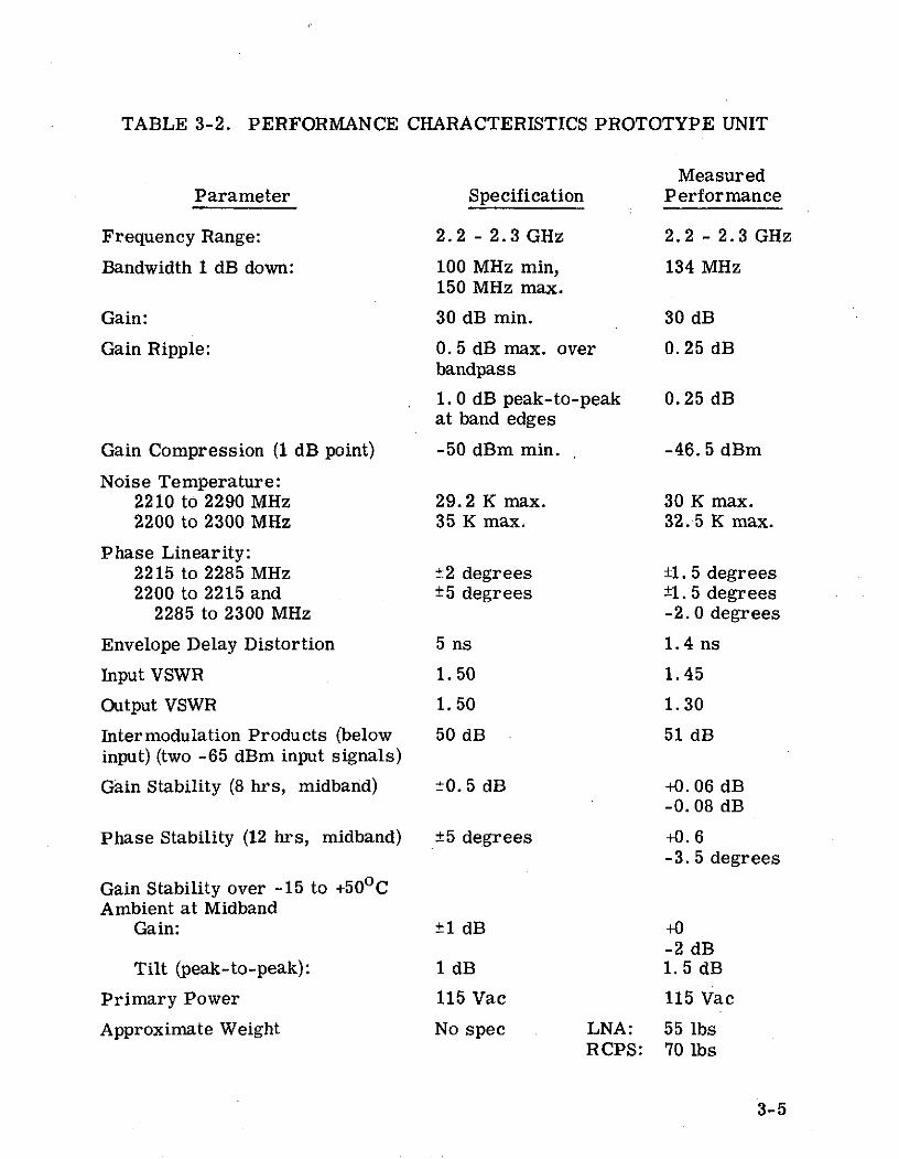
TABLE 3-2. PERFORMANCE CHARACTERISTICS PROTOTYPE UNIT
MeasuredParameter Specification Performance
Frequency Range: 2.2 - 2.3 GHz 2.2 - 2.3 GHz
Bandwidth 1 dB down: 100 MHz min, 134 MHz150 MHz max.
Gain: 30 dB min. 30 dB
Gain Ripple: 0. 5 dB max. over 0.25 dBbandpass
1.0 dB peak-to-peak 0.25 dBat band edges
Gain Compression (1 dB point) -50 dBm min. -46.5 dBm
Noise Temperature:2210 to 2290 MHz 29.2 K max. 30 K max.2200 to 2300 MHz 35 K max. 32.5 K max.
Phase Linearity:2215 to 2285 MHz ±2 degrees ±1. 5 degrees2200 to 2215 and +5 degrees ±1. 5 degrees
2285 to 2300 MHz -2.0 degrees
Envelope Delay Distortion 5 ns 1.4 ns
Input VSWR 1.50 1.45
Output VSWR 1.50 1.30
Intermodulation Products (below 50 dB 51 dBinput) (two -65 dBm input signals)
Gain Stability (8 hrs, midband) ±0. 5 dB +0. 06 dB-0. 08 dB
Phase Stability (12 hrs, midband) ±5 degrees +0. 6-3. 5 degrees
Gain Stability over -15 to +50 0 CAmbient at Midband
Gain: ±1 dB +0-2 dB
Tilt (peak-to-peak): 1 dB 1. 5 dB
Primary Power 115 Vac 115 Vac
Approximate Weight No spec LNA: 55 lbsRCPS: 70 lbs
3-5
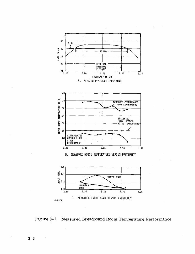
321 dB
30 136 MHz
S28
26 REQUIREDPASSBAND
24 2 STAGES
2.15 2.20 2.25 2.30 2.35
FREQUENCY IN GHz
A. MEASURED 2-STAGE PASSBAND
40
Y 38* MEASURED PERFORMANCE
AT ROOM TEMPERATURE
36
O 34- SPECIFIED
FINAL SYSTEM32 NOISE TEMPERATURE-
6 32
EXTRAPOLATED28 COOLED FIRST
STAGEPERFORMANCE
2.15 2.20 2.25 2.30 2.35
B. MEASURED NOISE TEMPERATURE VERSUS FREQUENCY
1.6
1.4
x PUMPED VSWRI 1.2
1.02.15 2.20 2.25 2.30 2.35
C. MEASURED INPUT VSWR VERSUS FREQUENCY4-1923
Figure 3-1. Measured Breadboard Room Temperature Performance
3-6
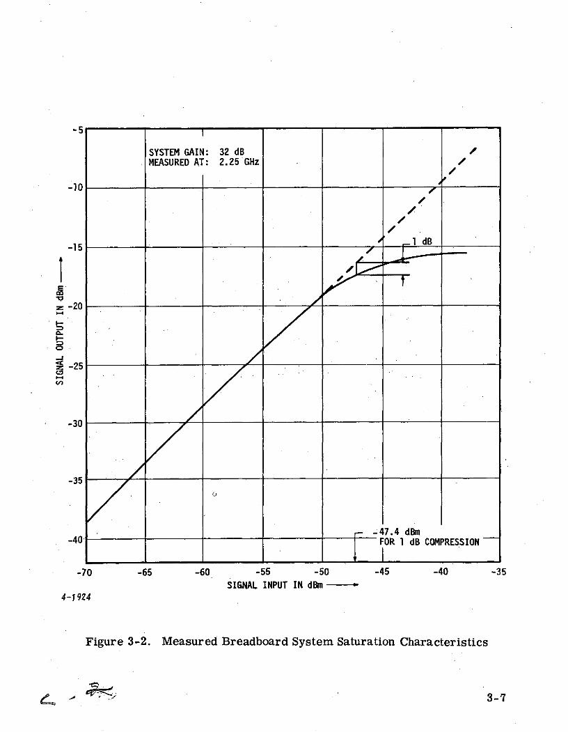
-5
SYSTEM GAIN: 32 dB /MEASURED AT: 2.25 GHz /
10
- dB-15
S-20
-25
-30
I-- /
-35
-47.4 dBm-40 IFOR 1 dB COMPRESSION
-70 -65 -60 -55 -50 -45 -40 -35SIGNAL INPUT IN dBi
4-1924
Figure 3-2. Measured Breadboard System Saturation Characteristics
3-7
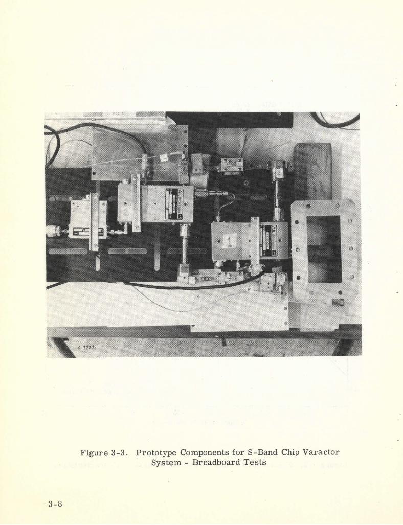
Figure 3-3. Prototype Components for S-Band Chip VaractorSystem - Breadboard Tests
3-8
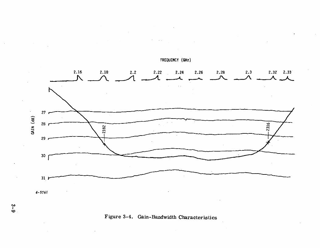
FREQUENCY (GHz)
2.16 2.18 2.2 2.22 2.24 2.26 2.28 2.3 2.32 2.33
27
28
29
30
31
4-3761
Figure 3-4. Gain-Bandwidth Characteristics
I
0
40
" 35
-J
w
L,
o 25
202.20 2.22 2.24 2.26 2.28 2.30
FREQUENCY (GHz)4-Figure 3-5. Noise Temperature Versus Frequenc55
Figure 3-5. Noise Temperature Versus Frequency
1.5
1.4
1.INPUTVSWR
OUTPUTVSWR
1.2
1.12.20 2.22 2.24 2.26 2.28 2.30
4-3156 FREQUENCY (GHz)
Figure 3-6. Input-Output VSWR Versus Frequency
-40
-46. dBA -1 dB
-50
I-
-60
-70-40 -30 -20 -10
INPUT POWER (dBm)4-3757
Figure 3-7. Dynamic Range Versus Frequency
3-12
+2
ADJUSTED AMPLIFIER PLOT
+1
,, i/ADJUSTED REF
-10
-5
2200 2215 2285 2300
4-3758 FREQUENCY (MHz)
Fiure 3-8. Phaseinearity Versus Fre.0uency
Figure 3-8. Phase Linearity Versus Frequency
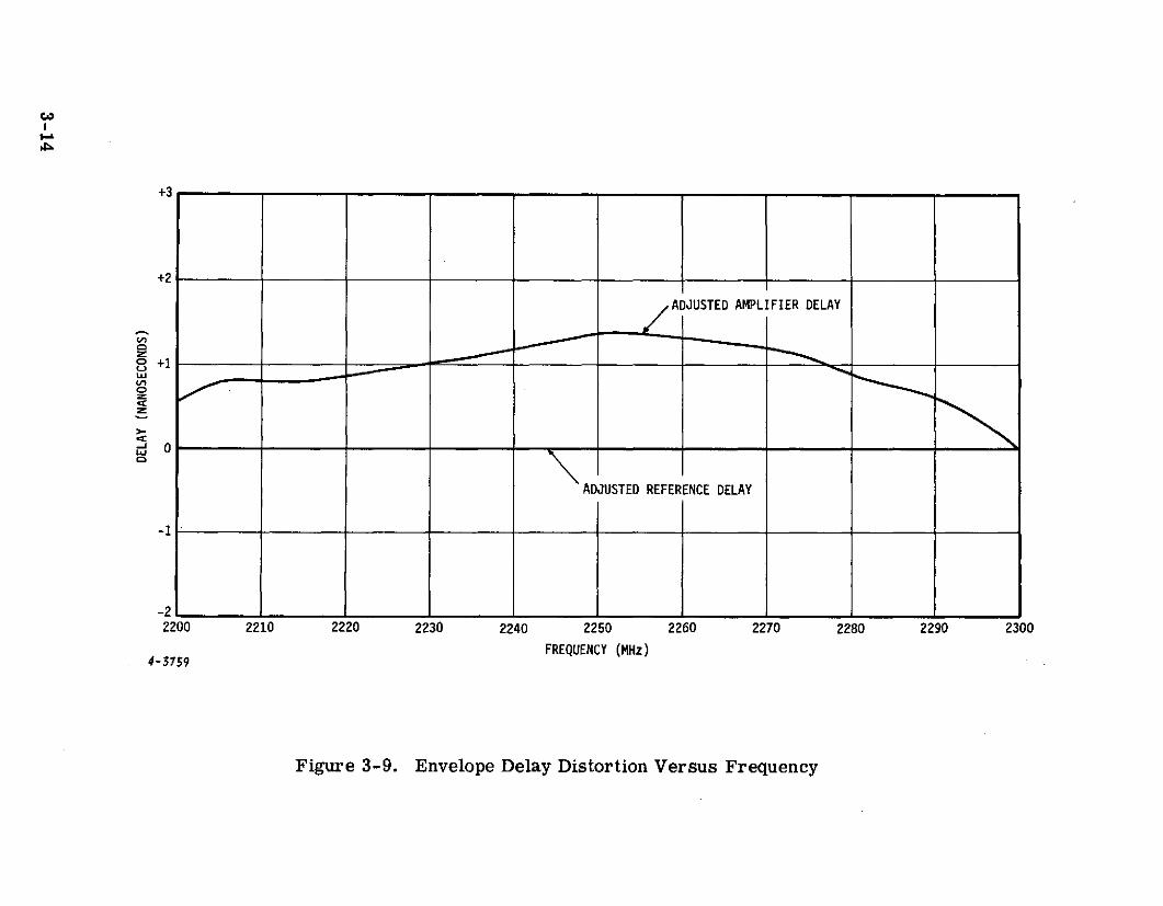
+3
+2
ADJUSTED AMPLIFIER DELAY
+1
0
ADJUSTED REFERENCE DELAY
-1
-22200 2210 2220 2230 2240 2250 2260 2270 2280 2290 2300
FREQUENCY (MHz)4-3759
Figure 3-9. Envelope Delay Distortion Versus Frequency
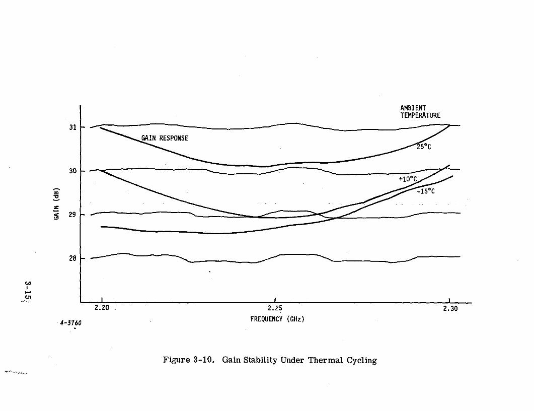
AMBIENTTEMPERATURE
31
GAIN RESPONSE250C
30+100C
-150C
S29
cI I
2.20 2.25 2.30
4-3760 FREQUENCY (GHz)
Figure 3-10. Gain Stability Under Thermal Cycling

No new technology was developed on this program.
4- 1
A. CONCLUSIONS
The S-Band Paramp System has successfully met all the major tech-nical requirements of the program. The design is such as to allow transitionto the production phase with a minimum of further engineering effort. Thesystem represents a significant advance in low-noise amplifier technology inthe following areas:
* Reduced Size, Weight and Power Consumption - Fig-ure 5-1 shows a comparison of size to an equivalentcryogenic system. The reduction in size can readilybe seen. The unit also requires less than one-thirdthe power of a cryogenic system
* Solid-State Reliability - The unit has no movingmechanical parts, such as compressors, cross-heads,pumps, etc., which require periodic maintenance andhave limited life. The only exceptions are four sim-ple blowers which can readily be replaced in the eventof failure and are of the sealed-bearing type requiringno maintenance
* Standby Performance in the Event of First StageCooler Failure - Unlike cryogenic systems, the sys-tem can be operated in the event of failure of thefirst-stage peltier cooler with slightly degradednoise temperature (30 to 37 K), increased inputVSWR, and slightly greater passband ripple
* Lower Initial Costs - Since no expensive cryogenicrefrigerator is required, the system will have lowerinitial and long-term operating costs
B. RECOMMENDATIONS
During the developmental effort and system testing, several areas ofpotential improvement were noted. These would be included in future
5-1
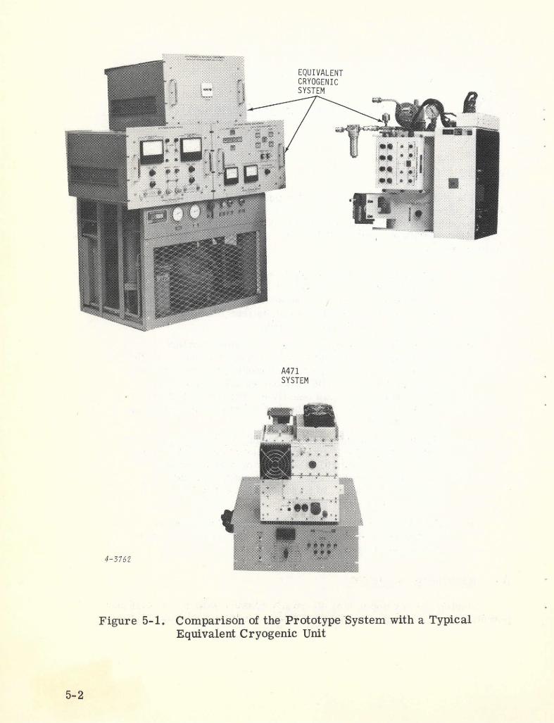
A471SYSTEM
4-3762
Figure 5-1. Comparison of the Prototype System with a TypicalEquivalent Cryogenic Unit
5-2
production units to improve performance, maintainability, and reliabilityas indicated below:
1. LNA MODULE (Figures 5-2, 5-3, and 5-4)
* Relocate Stage 1 GDO - This could be done by locatingthe stage 1 pump chain on the intercompartment bulk-heads as shown in Figure 5-3. This would allow useof a very short pump waveguide run. Changes in thepump waveguide ambient were found to be responsiblefor some thermal instabilities in the prototype model.By running the stage 1 pump line through a flexibleinsulating "pressure-tight" boot, the pump guide willtend to remain at a constant temperature over theambient range, since the GDO end is stabilized at50 0 C and the paramp end at -20 0 C. The waveguidewould be made of stainless steel which is thermallyisolating. This location and method of mounting wouldeliminate "tight" tolerances on location of the pumpline relative to the GDO assembly, since the flexibleboot could be made to accommodate up to +1/32 mis-alignment. The shield over the GDO compartmentwould tend to minimize convection currents fromchanging thermal distributions along the pump chain.
* Stabilize GDO's and Second-Stage at +60 0 C - Thiswould eliminate the necessity of using thermoelectricmodules and simplify the temperature controller cir-cuits. In addition, it would reduce "breathing" of theresponse due to "crossover" between thermoelectricand heater cycles. This would be possible due torecent improvement in the GDO which would allowsatisfactory operation to 60 0 C.
The revised packaging arrangement will greatly improve field main-tainability since GDO replacement and adjustment is greatly simplified.In addition, installation and removal of the lower drawer does not involvemating of assemblies which require close tolerances in their location rela-tive to each other,
Desiccator - A desiccator could be added to absorbmoisture in the first-stage compartment to eliminatethe need for a continuous supply of dry nitrogen.Every 3 months, the desiccator cartridge would bereplaced. This is presently being investigatedfurther on other AIL programs.
5-3
* Mount Entire Second Stage on One Temperature Stabil-
ized Plate (Figure 5-4) - The second stage GDO parampchain components would be mounted on a common therm-
ally isolated plate stabilized at 60 0 C. This would givemuch greater room in the lower compartment. In addi-
tion, this would improve maintainability since the entire
section can be removed as a unit.
* Printed Circuit Boards Mounted on GDO and Bias Regu-
lators (Figure 5-4) - Printed circuit boards mounted on
the voltage regulator pins would make a more compactreliable arrangement than the terminal boards used in
the prototype. The latter were used in the prototypeto facilitate adjustments and design changes.
* Filter Box - All wiring coming into the LNA enclosure
would be properly bypassed by use of a shielded filter
box as shown in Figure 5-4. All gaskets would be made
of conductive materials to eliminate potential EMI
problems.
Larger Lower Access Panel (Figure 5-2) - This would
facilitate adjustments of the GDO frequencies and allow
more ready access to interstage connections.
* High Power Darlington Heater Driver Transistors -
The use of high-power "Darlington" transistors would
reduce the number of discrete components in the tem-
perature controller circuit, therefore, improvingreliability.
* Revised Lower Drawer Gasketing - Since the lower
compartment would probably be pressurized in the
production units, an "L-shaped" frame as shown in
Figure 5-2 would probably be used. This would make
a simpler, more pressure-tight structure than the
shelf arrangement used in the prototype. This con-
struction is possible if 4 to 6 bolts can be employedon the bottom side of the unit to fasten the lower com-
partment assembly to the main frame.
5-4
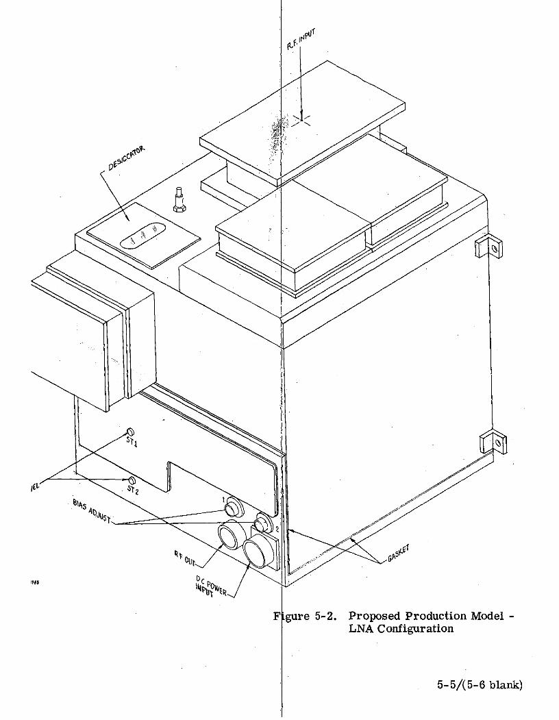
F gure 5-2. Proposed Production Model -LNA Configuration
5-5/(5-6 blank)
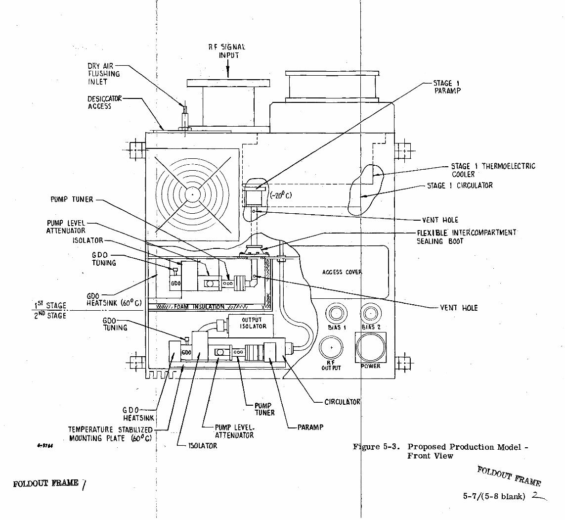
RF 5IGNALINPUT
DRY AIRFLUSHINGINLET STAGE I
PARAMPDESICCATORACCESS
STAGE 1 THERMOELECTRICCOOLER
---- - - STAGE I CIRCULATOR
PUMP TUNER
PUMP LEVEL VENT 14LEATTENUATOR FLXIBLE INTERCOMPARTMENT
SOLATO SEALING BOOT
GDOTUONING
Io .. ACCESS COVET
GDO15T STAGE 14EATSINK (600 G) -X ______VENT HOLE
2"' STAGE
TUNING' L R BIAS E 2
OUPUT POWER
CIRCULATORPUMPGDO TUNERHEATS5NK
TEMPERATURE STABILIZED PUMP LEVEL. PARAMPMOUNTING PLATE (600 C) ATTENUATOR
U - ISOLATOR Figure 5-3. Proposed Production Model -Front View
FOLDOUT lAME /a5-7/(5-8 blank) 2
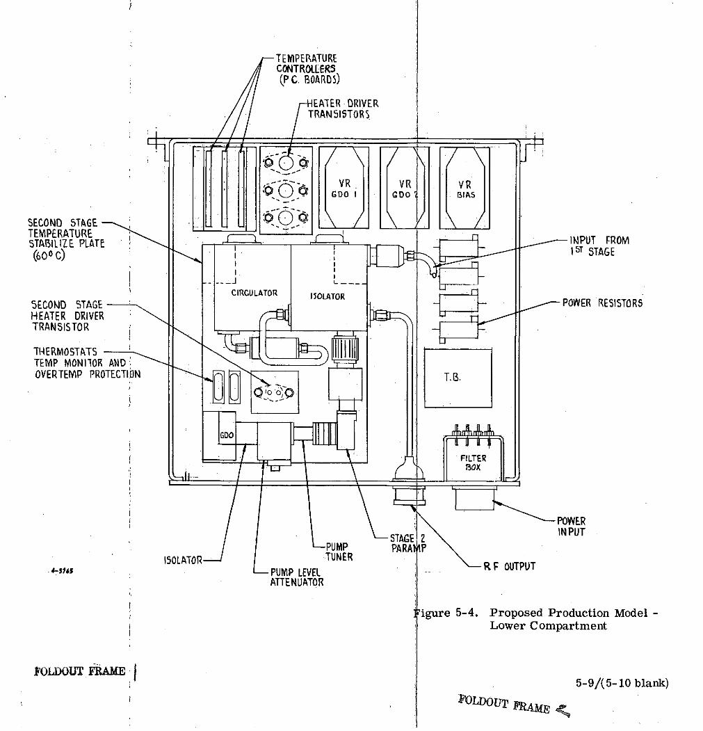
TEVPERATURECONTROLLERS(P C. BOARDS)
HEATER DRIVERTRANSISTORS
VR VR VR0GDo IGDo I As
SECOND STAGETEMPERATURE INPUT FROMSTABILIZE PLATE INPUT FROM(600C) I -- 1 STAGE
ECONDCIRCULATOR 5OLATOR POWER RESISTORS
HEATER DRIVERTRANSISTOR
THERMOSTATS ITEMP MONIIOR AND.OVERTEMP PROTECTION T.B.
FILTERo30X
POWER
STAGE 2 INPUTPUMP PARAMP
150LATOR TUNER.-sl i- _PUMP LEVEL
ATTENUATOR
igure 5-4. Proposed Production Model -Lower Compartment
FoLouT FAME5-9/(5-10 blank)
POLDOT To
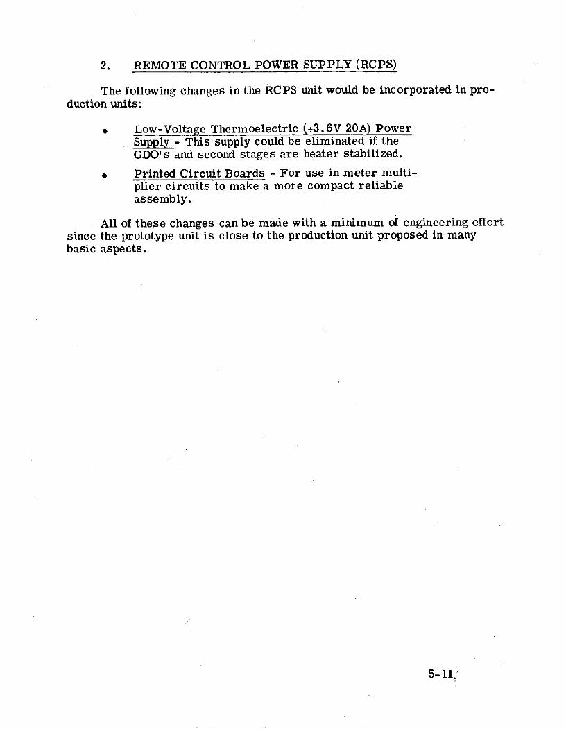
2. REMOTE CONTROL POWER SUPPLY (RCPS)
The following changes in the RCPS unit would be incorporated in pro-duction units:
* Low-Voltage Thermoelectric (+3.6V 20A) PowerSupply - This supply could be eliminated if theGDO's and second stages are heater stabilized.
* Printed Circuit Boards - For use in meter multi-plier circuits to make a more compact reliableassembly.
All of these changes can be made with a minimum of engineering effortsince the prototype unit is close to the production unit proposed in manybasic aspects.
5-11Z
1. P. Penfield, Jr. and R. P. Rafuse, "Varactor Applications," MITPress, Cambridge, Massachusetts, 1962.
2. J. R. Ashley and F. M. Polka, "Reduction of FM Noise in Micro-wave Diode Oscillators by Cavity and Injection Stabilization,"1971 GMTT International Microwave Symposium.
6-1 -

VII. APPENDIXES
Figure A-1 shows a three-port model for the pumped varactor.
Port 1 is at the input frequency (fl). Port 2 is at the idler or difference
frequency (f2 = f pump - fl). Port 3 is at the sum frequency (f3 = pump + fThis model was derived by an extension of the two-port analysis given by
Matthaei 1. The elements of the impedance matrix are given as follows:
11 Rs 1 L s 1 1 ); Z 1 2 = X 1 2 ; Z 1 3 = j X 1 3
Z21 = j X21; 22 = Rs2 + j (X2 2 - w2 Ls); Z2 3 = - j X 2 3
Z 3 1 = jX 3 1; Z3 2 =jX 3 2 ; Z 3 3 =Rs3 + (w 3 Ls- X 3 3)
where wl = 2 fl; 2 = 2? f2 ; W3 = 27 f3
and L s = series lead inductance
For generality different series resistances have been assumed
at each frequency. Also
C 21+
CoX11 = 2
CO[1+ C2 2 C 1
1 G. L. Matthaei, "A Study of the Optimum Design of Wide Band Para-
metric Amplifiers and Up-Converters," IRE Trans on Microwave
Theory and Techniques. January 1961.
A-1
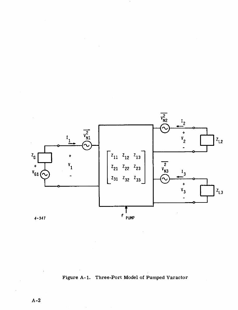
Z2
ZG + Z11 212 Z13
1 21 V22 23 V
V3 ZL3
4-347 f PUMP
Figure A-i. Three-Port Model of Pumped Varactor
A-2
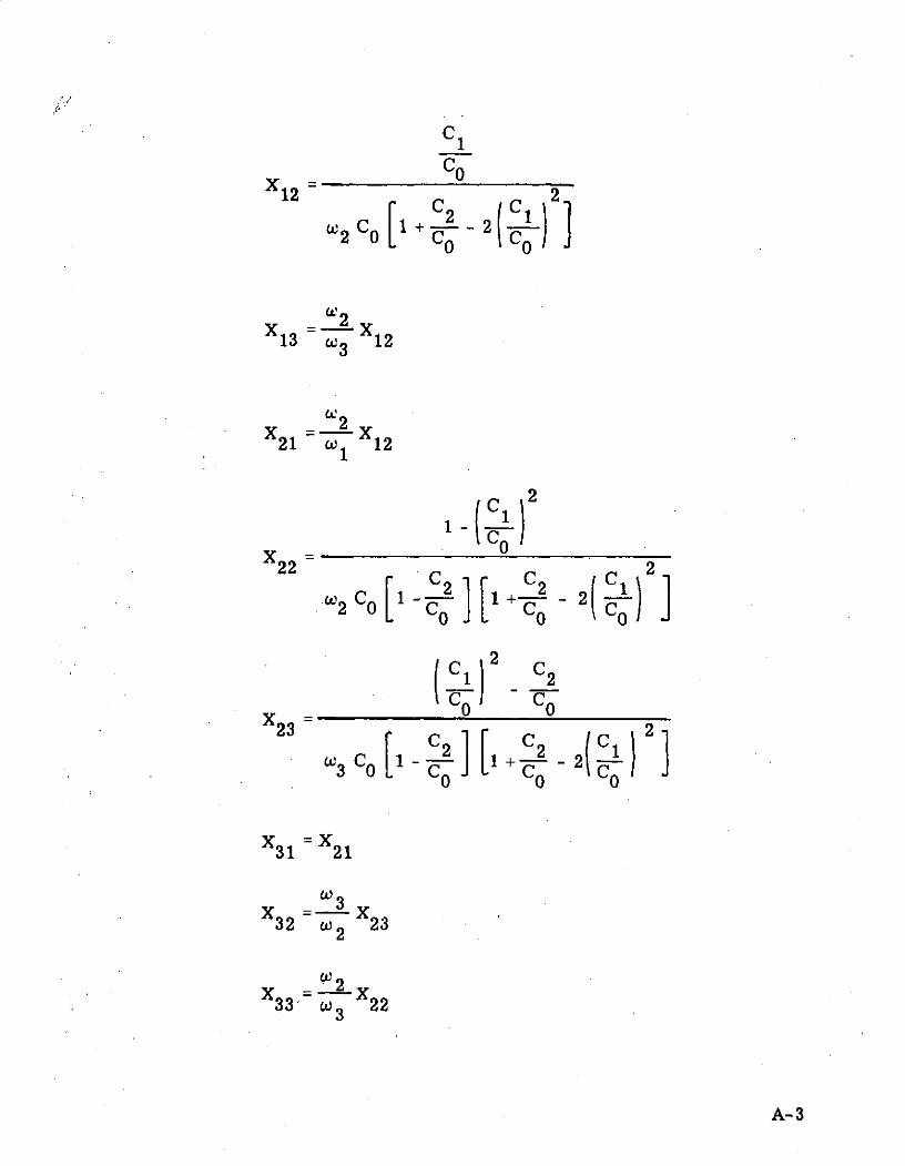
C 1
CO
12= 2
2 C + -2
x1213 = 12
SCL221 w 12
11 )2
22 C2 C2
02 CO I-C- + C 2 cC C C
2 1 12 2
X3 1 21
W 3 2
X33' X22
A-3
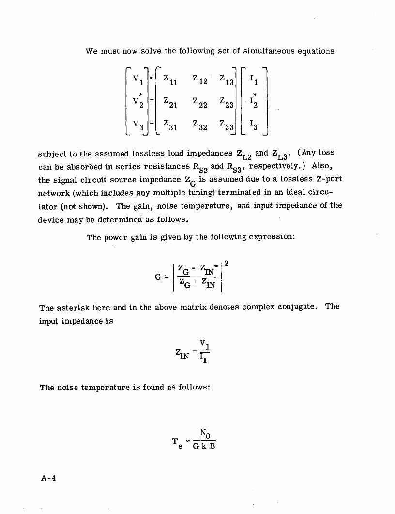
We must now solve the following set of simultaneous equations
V =1 Z1 1 Z 1 2 z13 1
V2 Z21 Z22 Z23 12
V3 Z31 Z32 Z33 3
subject to the assumed lossless load impedances ZL2 and ZL3. (Any loss
can be absorbed in series resistances RS2 and RS3 , respectively.) Also,
the signal circuit source impedance ZG is assumed due to a lossless Z-port
network (which includes any multiple tuning) terminated in an ideal circu-
lator (not shown). The gain, noise temperature, and input impedance of the
device may be determined as follows.
The power gain is given by the following expression:
ZG - ZIN*G=
ZG + ZIN
The asterisk here and in the above matrix denotes complex conjugate. The
input impedance is
V 1
The noise temperature is found as follows:
No
e GkB
A-4
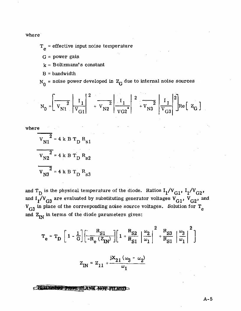
where
Te = effective input noise temperature
G = power gain
k = Boltzmann's constant
B = bandwidth
NO = noise power developed in ZG due to internal noise sources
2 '1 2 1 2 10 NO= N1 V N 2 +VN 3 V e GJ
GI VG2 G3
where
2VN1 =4kBT RN1 D sl
V 2 =4kBT RN2 D s2
2VN3 =4kBT D Rs 3
and TD is the physical temperature of the diode. Ratios Il/VG1, I1/VG2'and I1/VG3 are evaluated by substituting generator voltages VG1, VG 2 , and
VG 3 in place of the corresponding noise source voltages. Solution for Te
and ZIN in terms of the diode parameters gives:
2 2RS, R2 R 2T=T 1- + DSi R S2 2 R 3
De D G R S1 W1 R 1 WJ J
jX2 1 (w 3 -2)ZIN = Zll +
A-5
where
W1 = (Z 2 2 + ZL2*) (Z 3 3 + ZL3) - X 2 3 X 3 2
2 = -jX 1 2 (Z 3 3 + ZL 3 ) + X 1 3 X 3 2
w3 = -X 1 3 (Z 2 2 + ZL 2 *) - X12 X23
The asterisk denotes complex conjugate.
A computer program to find the solution to these equations was
developed by modeling the load impedances ZL2 and ZL3 to include varactor
package capacitance and the dimensions of the waveguide mount. Similar
modeling of the coaxial signal circuit was included. "Tuning up" of the
parametric amplifier on the computer for symmetrical responses and the
proper gain can be accomplished by proper choice of parameter values.
The program is basically intended for the balanced parametric amplifier,
where the signal circuit is geometrically isolated from the idler and sum
circuits. Slight modifications are necessary for other types of mounts
(single-ended, all waveguide, etc.).
A-6
APPENDIX B
GAIN CHANGES AS A FUNCTION OF CIRCULATORISOLATION CHANGES
The active gain of the parametric amplifier depends criticallyon the interaction between the complex reflection coefficient looking into theamplifier port of the circulator and the inherent reflection coefficient of theamplifier. For an almost lossless circulator with high isolation, the netreflection coefficient (complex voltage gain) is approximately given by:
r = Ir lej = m (B-1)r . e
nom1-
1
L.2
where
rnom = nominal value of r for unity SWR of the circulator
L. = nominal magnitude of port-to-port circulator isolation
0 = net phase difference between circulator and amplifier
1
1 rI = magnitude of r = K
0 = phase of r
Differentiating equation H-1 yields the fractional change:
K 2 1 A Li j (0+0) (B-2)S 2 L.
B-1
From equation H-1, the general expression for fractional change of power
gain K(K = r 12) is:
AK 2A - (B-3)
where the asterisk denotes complex conjugate.
Substitution of equation H-1 into equation H-3 yields:
1
A] [ = -A cos(O + 0) + 2A0 sin(O + ) (B-4)K L
Dealing with a relatively narrow band situation, where 0 and $ will notvary appreciably over the band, it is possible to operate with either (0 + 0)i/2 or w, which would mitigate gain changes due to AL. or AO, respectively.Assuming the latter case, equation H-4 reduces to:
1
. . (B-5)K L.
B-2
APPENDIX C
NOISE TRANSFER ANALYSIS--SINGLE STAGEPARAMETRIC AMPLIFIER
1. INTRODUCTION
Since the noise of a pump source will cause a random fluctuation ininstantaneous pump power, the varactor capacitance will fluctuate accordingly.Because of this it will be shown that the pump noise is downconverted into thesignal frequency domain, thereby degrading the tangential sensitivity of theamplifier.
For normal operation, even with a noisy pump, this degradation isoften negligible. However, it has been observed that when a strong interfer-ing signal is present in close proximity of the received frequency, a severedegradation in tangential sensitivity occurred. In this case, the pump-derived noise side bands of the strong interfering signal increase the inputnoise level at the received frequency. This phenomenon will be explained,and an expression for the degradation of the tangential sensitivity as a func-tion of the strength of the interfering signal will be derived.
2. ANALYSIS
Consider an amplitude modulated signal,
aA (1 + ; cos pt) sin wt
where A and a denote peak amplitudes.
As is well known the frequency spectrum of this signal is given byFigure C -1.
C-1
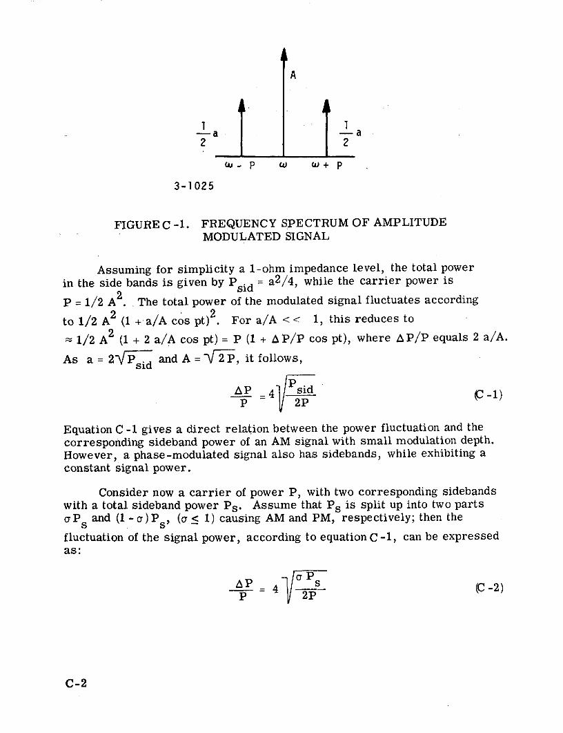
A
1 1-a -a
2 2
u- p w w+ P
3-1025
FIGURE C -1. FREQUENCY SPECTRUM OF AMPLITUDEMODULATED SIGNAL
Assuming for simplicity a 1-ohm impedance level, the total powerin the side bands is given by Psid = a 2 /4, while the carrier power is
P = 1/2 A 2 . .The total power of the modulated signal fluctuates according
to 1/2A 2 (1 +a/Acos pt) . For a/A < < 1, this reduces to
; 1/2 A 2 (1 + 2 a/A cos pt) = P (1 + AP/P cos pt), where A P/P equals 2 a/A.
As a = 2 and A = '2P, it follows,sid
AP =4 -1)P - 2P
Equation C -1 gives a direct relation between the power fluctuation and thecorresponding sideband power of an AM signal with small modulation depth.However, a phase-modulated signal also has sidebands, while exhibiting aconstant signal power.
Consider now a carrier of power P, with two corresponding sidebandswith a total sideband power Ps. Assume that Ps is split up into two partsuPs and (1- a)Ps, (a < 1) causing AM and PM, respectively; then the
fluctuation of the signal power, according to equation C -1, can be expressedas:
SP- 4 Ps (C -2)P 2P
C-2
Pure AM or FM can only be obtained when there is a 100 percentcorrelation between the corresponding sidebands. They have to be of equalamplitude and must have a specific phase relation to make it either pureAM or pure FM.
When there is no correlation between the two sidebands, for example,when the sidebands consist of noise components with random phase andamplitude characteristics, we can assume that the average total sidebandpower will be equally distributed between AM and FM which means that inequation C -2, a = 1/2.
When passing this spectrum through a nonlinear device, however, thenonlinearity will generally cause the sidebands of the output spectrum to becorrelated to some degree.
As an oscillator is basically a nonlinear device, it is to be expected thatthere will be some correlation between its noise sidebands (a # 1/2).
The proper value of a will be determined by the physical mechanismof frequency generation.
Assume a parametric amplifier with a pump source P (watts) atp
frequency f and tuned to a signal frequency f so that the idler frequency
f. = f - f . These frequencies are indicated on a spectral diagram Figure C -2.I p s
Also indicated is the noise spectrum of the pump source and a strong in-terfering signal fs (&f) = fs - Af of power PS( f), and the corresponding
idler frequency fi (if)*
Consider a noise packet around the frequency f = f + Af of widthn p6 f and containing a power APn. The spectral noise power density is then
P(f) = APn/6 f watts/Hz.
As was explained above, this noisy power quantity with its corre-sponding sideband (AP at f - Af) will cause amplitude as well as frequency
modulation of the pump signal. Frequency variations of the pump signalcause corresponding frequency changes in the idler. If the bandwidth ofthe idler circuit is large, however, these frequency variations will not benoticed in the signal circuit.
C-3
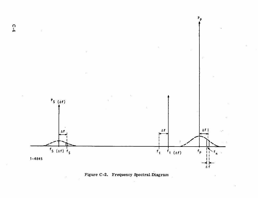
Pp
PS (Af)
A. Af Afl
s (Af)fs fi fi (Af) fP II
1-4845 II
6f
Figure C-2. Frequency Spectral Diagram
Thus, only the amplitude modulation of the pump is of interest.
The amplitude, A P, of the variation in instantaneous pump-power(noise around frequency FM) can be found from equationC -2. With
PS = 2 A Pn (APn represents only one sideband) we find:
a A Pn= 4 (C-3)
P Pp p
The change in gain of a parametric amplifier as a result of a change in pumppower is given by (reference 1, equation 10:40)
AK K1/2 p (C-4)K P
p
The equivalent change of the input power of the interfering signal PS f)is therefore:
P K1/2 AP
s(Af) p S( f) (C-5)
Substitution of C -3 into C -5 yields:
A (f) = 4K 1 /2 Ja A n (C-6)
S(Af) p
This induced noise modulation of PS is pure AM giving two correlated
noise sidebands at fs(f) Af = fs - 2 Af and fs(Af)+ Af = fs, thus(Af)
degrading the tangential sensitivity at f = f .
The corresponding induced noise power APni in each sideband can be
found with the aid of equation C-2. With a = 1 and PS = 2 AlPn.
A-Ps('f) APniPSf S(f)
C-5
Equating C-6 and C-7 yields:
n. P S
If the noise temperatures of the amplifier and the signal source areTA and TS, respectively, the operational temperature is defined as
op A + TS
The tangential sensitivity in the absence of an interfering signal is:
P =kT *B(fs) op
where:
B = system bandwidth
k = Boltzman's constant = 1.38 x 10⁻²³ Joules/K
As was pointed out, the interfering signal PS(A f) increases the noise
background at f = fs from:
k T B to k T B+K n BPop op P S
where (APn)B is the noise power content of the noise spectrum between
the frequencies f - B/2 and fn + B/2 is:
fn + B/2
(APn)B (f) df
f -B/2
This, for small B, can be approximated by:
(APn) B P(fn) B
C-6
so that the tangential sensitivity at f = fs in, the presence of the interferingsignal can be written as:
ap(f n) BP =kT B+K P
T(fAf) op P S(Af)
The tangential sensitivity, therefore, is degraded by the factor:
T(fsf) P(fn)
= 1+K PP kT P s
T(f) op p s(f)
Defining the normalized spectral power density as:
W a n) (second)(Af)- p
(fs Af) K=1+ F P
PTf T (Af) f)T op
(fs)
whereW
F (Af)(Af) k
can be regarded as a figure of merit for the pump source of a parametricamplifier.
C-7
3. CONCLUSION
It has been derived that the degradation in tangential sensitivity for asingle-stage paramp at f = fs as a result of a strong interfering signal
Af away, is given by:
T(fs Af) K ]= 1+ F P
T (f) op (Af)
where
PT = tangential sensitivity at f = fs in the presence of an
(fsf) interfering signal Af awayP
(fs) = tangential sensitivity at f = fs
K = power gain of amplifier
T = operational temperatureop(Top = Tamplifier + T signal-source )
( k(Af) figure of merit of pump source
W = normalized AM spectral noise power density of pumposcillator Af away from carrier
k = Boltzmann's constant = 1.38 x 10⁻²³ Joules/K
P = power of interfering signal Af away from fs (f)s
In FigureC -3, this relation PT s f T(f) is shown graphically as a
function of Ps ) with K/TopJ F(Af) as parameter.
C-8
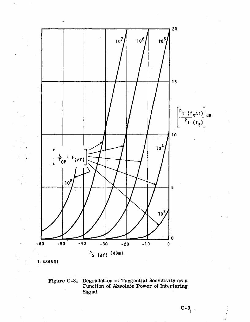
20
107 106 10
15
[ T (f Af)
T (f )
10
S104
108
103
-60 -50 -40 -30 -20 -10 0
PS (Af) (dBm)
1-4846RI
Figure C-3. Degradation of Tangential Sensitivity as aFunction of Absolute Power of InterferingSignal
C-9,

APPENDIX D
TEST PROCEDURE FOR EVALUATION OFNON-HERMETICALLY SEALED GALLIUM
ARSENIDE VARACTOR
D-1
DASH APPLICATION REVISIONSNO. NEXT ASSY USED ON LTR DESCRIPTION DATE APPROVED
THIS DRAWINGINCOMPLETE
WITHOUT ECN'S
APPENDIX D
TFST PROCEDURF
FOR
EVALUATION OF NON-HERMETICALLY SEALED
GALLIUM ARSENIDF VARACTOR
!All PROPRIETARY INFORMATION
LTR
SHEET
LTRSHEET 32 33 34 35 36 37 38 39 40 41 42 43 44 45 46 47 48 49 50 51 52 53 54 55 56 57 58 59 60 61
LTR
SHEET 2 3 4 5 6 7 8 910 11 12 13 14 15: 1 7 18 19 20 21 22 23 24 25 26 27 28 29 30 31
ALL PAGES ARE OF CONTR NO. AIL ais..ion. oORIGINAL ISSUE (A) PR BY cutLA-HAmmER ......... .. Wv.....
EXCEPT AS NOTED. CHK BYREVIEW EVAULATION OF NON-HERMFTICALLY SFALED
ENGR (PROJ) GALLIUM ARSENIDE VARACTOR
PP (RaJ,) SIZE CODE IDENT NO.
V A 00752 381722APIROVAL (GOVT)
SCALE SHEET 1 OF 22
l-F-333 R D-3
Preceding page blank
1.0 PURPOSE OF TFST
This document formulates the test procedures that will be
followed for the Fvaluation of the Non-Hermetically Sealed Gallium
Arsenide Varactor, AIL Part No. 381701.
The order of the tests are to be followed as indicated with
no deviations.
AL RPITARY NFORATIO
SIZE CODE IDENT NO.
AIL- Or..... A 00752 - 381722D0 PARK. LOW* ISLAND NEW YORN 1179
SCALE !SHEET 2 REV
AL-F- 335 RI
D-4
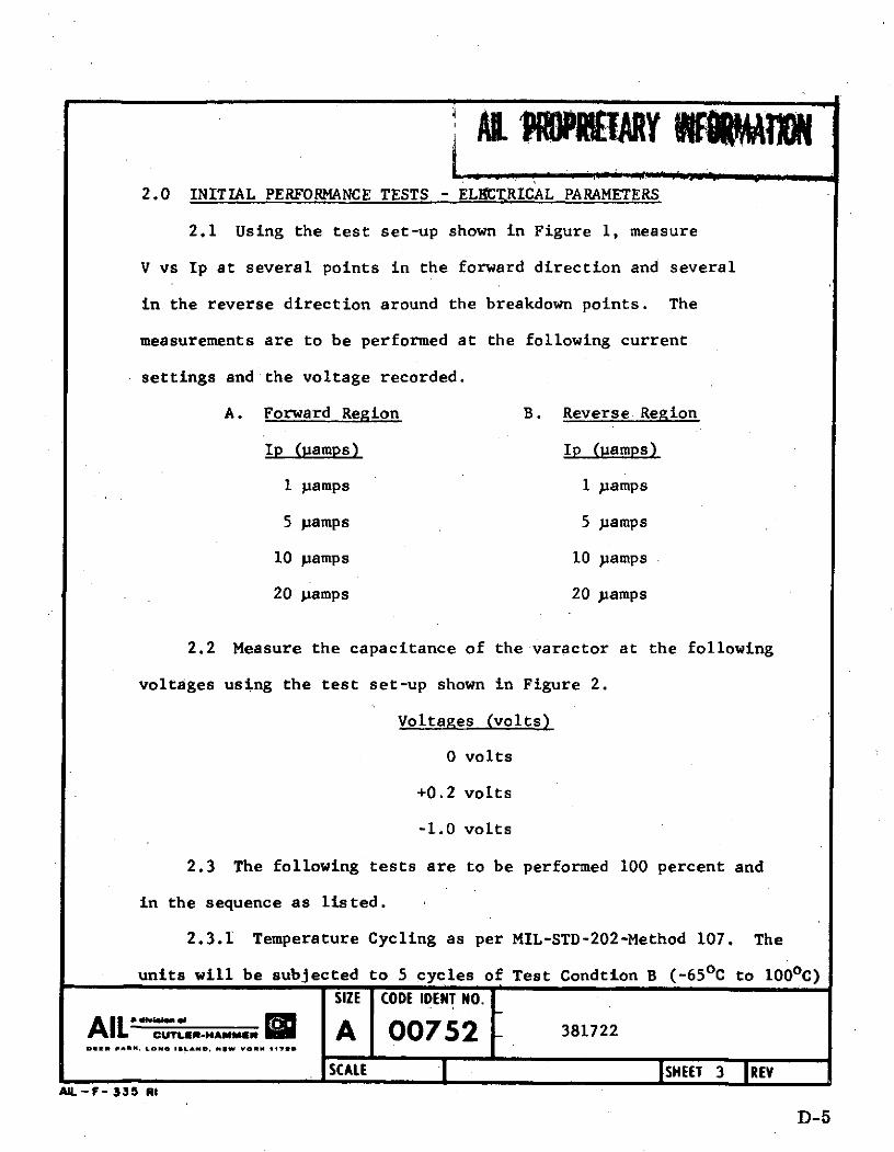
2.0 INITIAL PERFORMANCE TESTS - EL)CTRICAL PARAMETERS
2.1 Using the test set-up shown in Figure 1, measure
V vs Ip at several points in the forward direction and several
in the reverse direction around the breakdown points. The
measurements are to be performed at the following current
settings and the voltage recorded.
A. Forward Region B. Reverse Region
Ip (pamps) Ip (pamps)
1 pamps 1 pamps
5 pamps 5 pamps
10 pamps 10 )amps
20 pamps 20 pamps
2.2 Measure the capacitance of the varactor at the following
voltages using the test set-up shown in Figure 2.
Voltages (volts)
0 volts
+0.2 volts
-1.0 volts
2.3 The following tests are to be performed 100 percent and
in the sequence as listed.
2.3.1 Temperature Cycling as per MIL-STD-202-Method 107. The
units will be subjected to 5 cycles of Test Condtion B (-65 0 C to 1000C)
SIZE CODE IDENT NO.
AIL* CUTLE..HAMME. A 00752 381722ODWW PAWM. LONG *SLAND, N6W YORKM 170
SCALE ISHEET 3 REVAIL-F- 335 RI
D-5
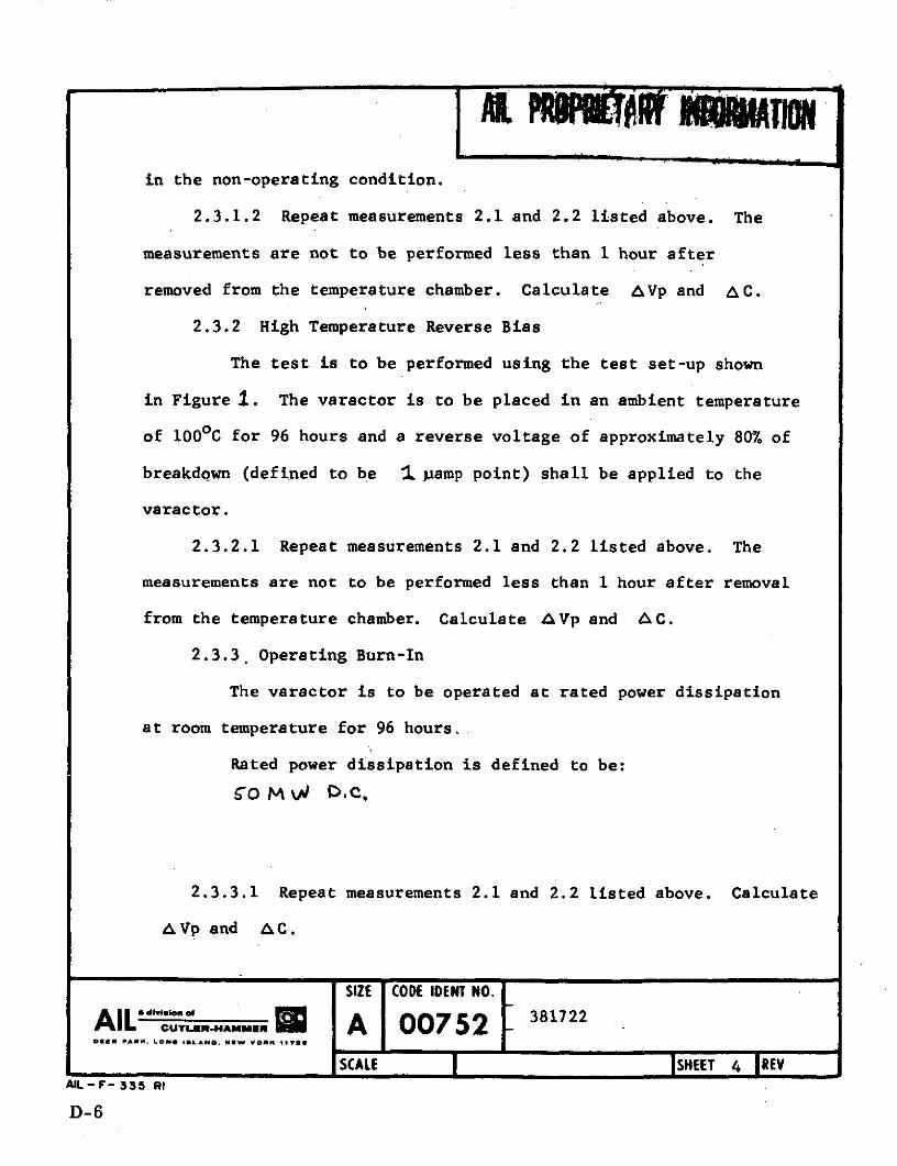
S"m"'- P "'',E "ff aB Qs1lll1
in the non-operating condition.
2.3.1.2 Repeat measurements 2.1 and 2.2 listed above. The
measurements are not to be performed less than 1 hour after
removed from the temperature chamber. Calculate AVp and AC.
2.3.2 High Temperature Reverse Bias
The test is to be performed using the test set-up shown
in Figure 1. The varactor is to be placed in an ambient temperature
of 100 0C for 96 hours and a reverse voltage of approximately 80% of
breakdown (defined to be p pamp point) shall be applied to the
varactor.
2.3.2.1 Repeat measurements 2.1 and 2.2 listed above. The
measurements are not to be performed less than 1 hour after removal
from the temperature chamber. Calculate AVp and AC.
2.3.3, Operating Burn-In
The varactor is to be operated at rated power dissipation
at room temperature for 96 hours.,
Rated power dissipation is defined to be:
2.3.3.1 Repeat measurements 2.1 and 2.2 listed above. Calculate
AVp and AC.
SIZE CODE IDENT NO.
AILO dTLR.HAM.. = U A 00752 81722D0 ER PAM,. LONG SLAN ND. W VOnM 1179
SCALE SHEET 4 REVAL-F- 335 RI
D-6
j IWRIEJARY WORWAI2.4 This series of tests are then concluded. The varactor
will then be subjected to either the Operating Life Test or the
Storage Life Test. This shall be so indicated on the Test Data
Sheets.
2.5 Operating Life Test
The varactor shall be operated at rated power dissipation
and an ambient temperature of 250C for 50 minutes ON and 10 minutes
OFF for a total time of 960 hours. Measurements shall be made per
2.1 and 2.2 at 0, 160, 480, and 960 hours. Calculate AVp and AC.
2.6 Storage Life
The varactor shall be subjected to a storage life test of
+100 0 C without power applied for a period of 960 hours. Measurement
shall be made per 2.1 and 2.2 at 0, 160, 480, and 960 hours.
Calculate AVp and AC. The measurements are not to be performed
less than 1 hour after removal from the temperature chamber.
SIZE CODE IDENT NO. 0
AIL CUTLA.......MM A 00752 381722OD61 PAR. LON* IGLAND. NOW YOR 1t1700
SCALE SHEET 5 iREVAL-F-335 RI
D-7
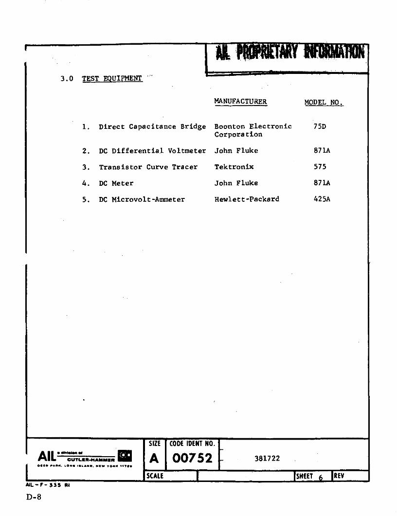
3.0 TEST EQUIPMENT
MANUFACTURER MODEL NO.
i. Direct Capacitance Bridge Boonton Electronic 75DCorporation
2. DC Differential Voltmeter John Fluke 871A
3. Transistor Curve Tracer Tektronix 575
4. DC Meter John Fluke 871A
5. DC Microvolt-Ammeter Hewlett-Packard 425A
SIZE CODE IDENT NO.
AIL 'UTL" UMR A 00752 381722I Ol lES PA , LOe ISLAND. N1W YORK IITI
SSCALE I ISHEET IREVAIL-F- 335 RI
D-8
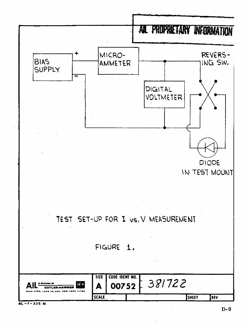
M\cRO- VERS-BIAS AMMETER IiG SW,SUPPLY
VOLTMETER
DODE\W TEST MOUT
TEST SET-UP FOR I vs.V MEASUREMEWT
FIGURE i.
SIZE CODE IDENT NO.
AIL CUSiu.....mi. A 00752 F3 /72 2OmanA ARi. LON* IGLAND. NoW VOlK 412 1 ,. 1
SCALE SHEET REVAlL-F- 335 RI
D-9
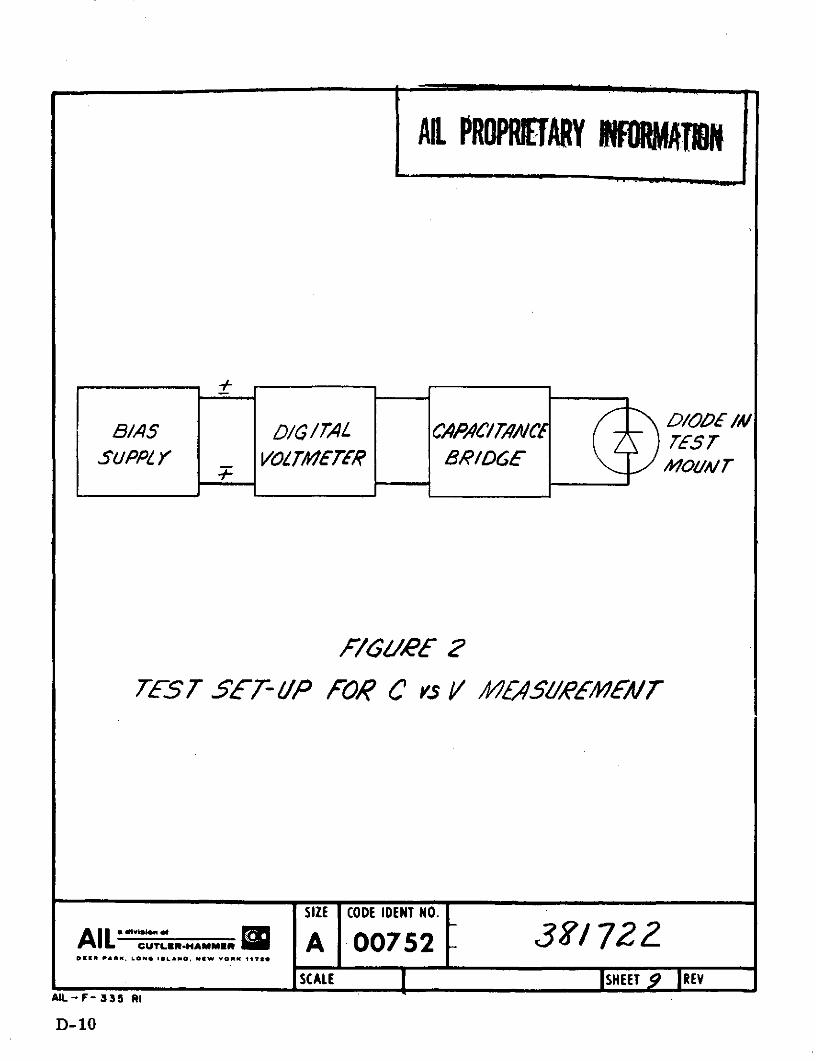
8/AS D/G /AL CAPAC/M7A/CTSUPPL ( VOLTMETER BR/DGE ,O&n ,
F/6U/2E 2
TEST 7SE T- IP FOR C vs VI/ E45/1PM6ENA/T7"
SIZE CODE IDENT NO.
AIL CUL.....HM..EM A 00752 3 722DiR PA M. LONe I LADO, *W YOIN 9171t SSCALE ISHEET IREV
AlL-F- 335 RI
D-10
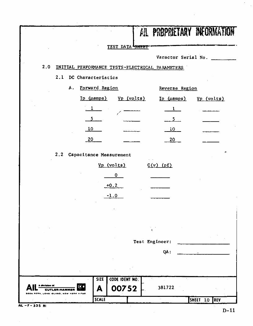
Al PRBPRETARY ORMARTEST DATA '
Varactor Serial No.
2.0 INITIAL PERFORMANCE TESTS-ELECTRICAL PARAMETERS
2.1 DC Characteristics
A. Forward Region Reverse Region
Ip (Pamps) Vp (volts) Ip (jamps) Vp (volts)
1 i
5 5
10 10
20 20
2.2 Capacitance Measurement
Vp (volts) C(v) (pf)
0
+0.2
-1.0
Test Engineer:
QA :
SIZE CODE IDENT NO.
AIL CU.,,.,.... E A 00752 381722DUK PArK. LONe SLANOD. NW VOE 1~7o
__ _ _ AO .L N_@A D_ _ __ _ _70 SCALE SHEET 10 REV
AL -F- 335 RI
D-11
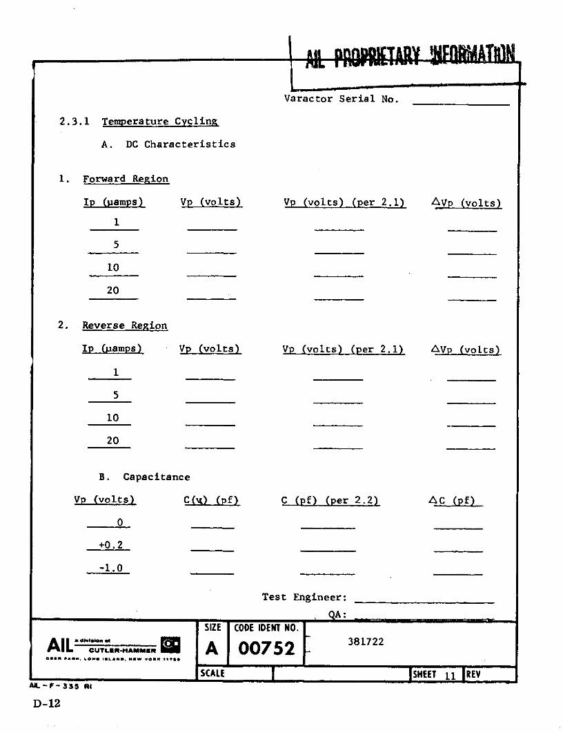
Varactor Serial No.
2.3.1 Temperature Cycling
A. DC Characteristics
1. Forward Region
Ip (pamps) Vp (volts) Vp (volts) (per 2.1) Avp (volts)
1
5
10
20
2. Reverse Region
Ip (jamps) Vp (volts) Vp (volts) (per 2.1) AVp (volts)
I
5
10
20
B. Capacitance
Vp (volts) C(N) (pf) C (pf) (per 2.2) AC (pf)
0
+0.2
-1.0
Test Engineer:
QA:SIZE CODE IDENT NO.
AIL .A 00752 381722
ODIa PAm, LO 1LA*D. HIMW YOM 07e2
SCALE SHEET 11 REV
AlL-F- 335 RI
D-12
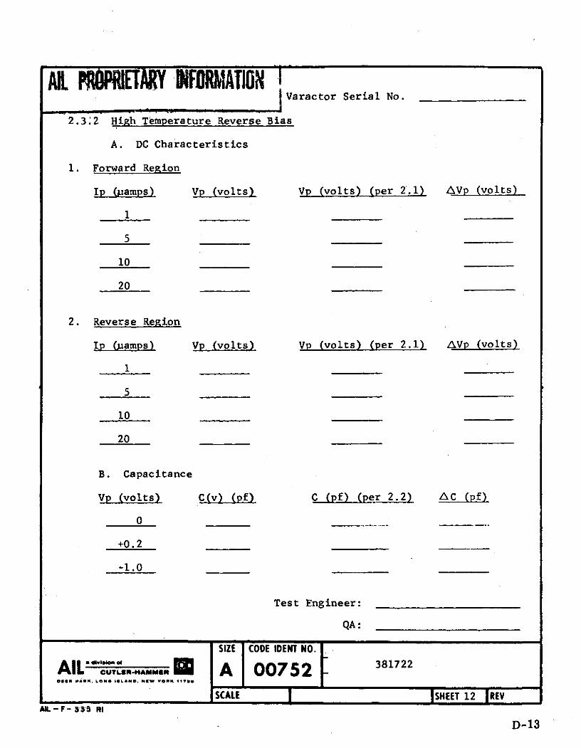
AL PRWPIlETARY FRMATIONVaractor Serial No.
2.3.2 High Temperature Reverse Bias
A. DC Characteristics
1. Forward Region
Ip (jamps) Vp (volts) Vp (volts) (per 2.1) AVp (volts)
i
5
10
20
2. Reverse Region
Ip (pamps) Vp (volts) Vp (volts) (per 2.1) AVp (volts)
1
5
10
20
B. Capacitance
Vp (volts) C(v) (pf) C (pf) (per 2.2) AC (pf)
+0.2
-1.0
Test Engineer:
QA:
SIZE CODE IDENT NO.Ai of 381722AILO CTL........ E A 00752 381722
OSM PAnM. LONO *LAN*. NlW wORm '174l
SCALE ISHEET 12 REV
AL - F - 35 RI
D-13
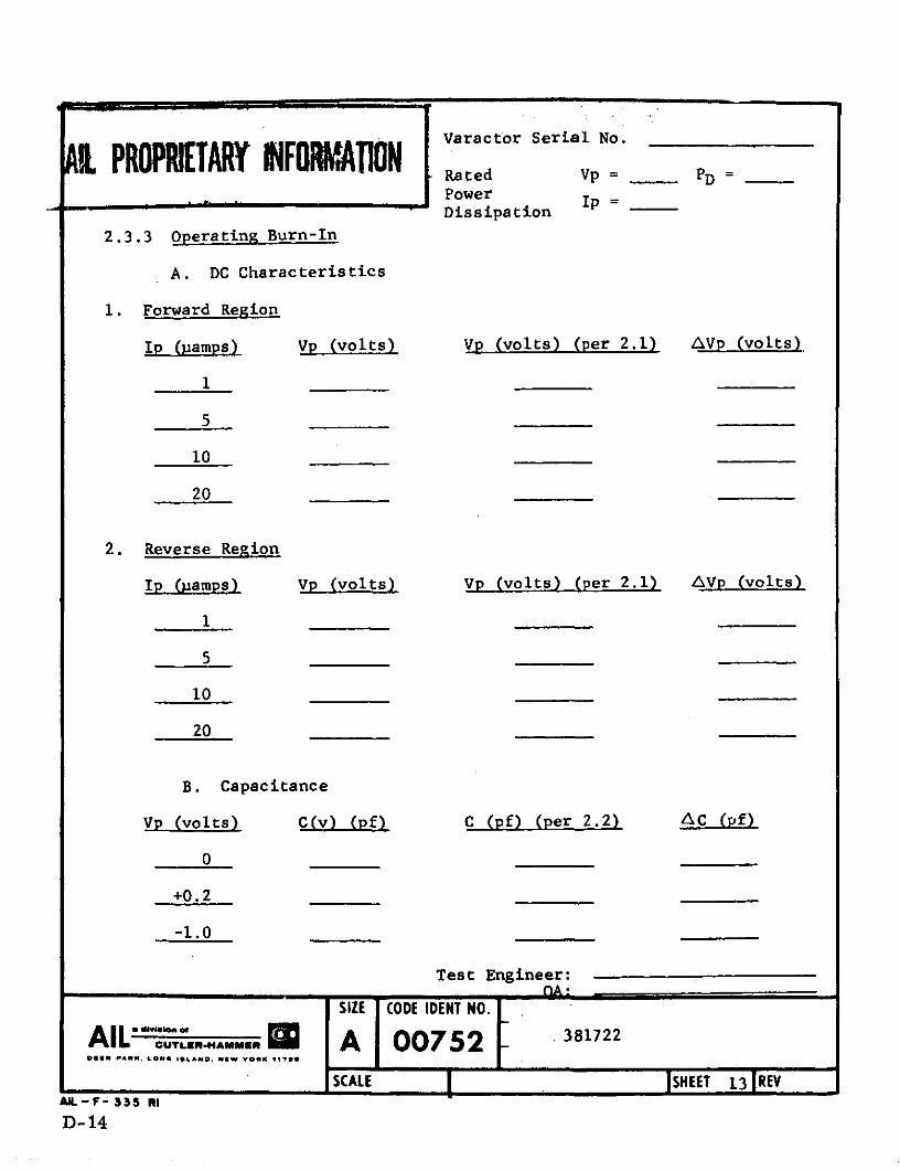
Varactor Serial No.
At PROPRIETARY iFO ATION Rated Vp= PDRated VpPower Ip =Dissipation
2.3.3 Operating Burn-In
A. DC Characteristics
1. Forward Region
Ip (pamps) Vp (volts) Vp (volts) (per 2.1) AVp (volts)
1
5
10
20
2. Reverse Region
Ip (Oamps) Vp (volts) Vp (volts) (per 2.1) AVp (volts)
i1
5
10
20
B. Capacitance
Vp (volts) C(v) (pf) C (pf) (per 2.2) AC (pf)
0
+0.2
-1.0
Test Engineer:
SIZE CODE IDENT NO.
AIL" ' .CUTLR HME A 00752 - 381722Dolg PAR N, LONR ILAND. N W YOmm 179 1
SCALE I ISHEET 13 REVAL- F-1335 I1
D-14
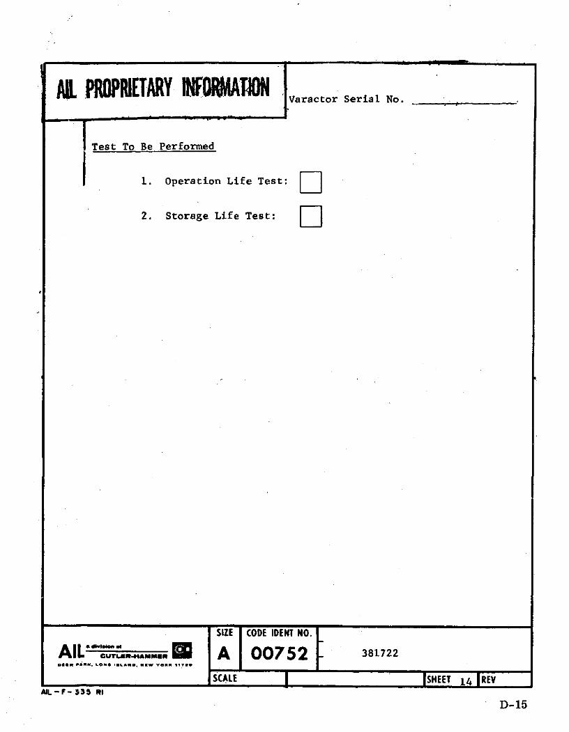
SPROPRIETARY IORMAON Varactor Serial No.
Test To Be Performed
I. Operation Life Test: D2. Storage Life Test:
SIZE CODE IDENT NO.
AIL CUTLER.HAm.m MA 00752 381722oWW PAMU. LOWS S LAND, NIW YOMM 11*72
SCALE ISHEET 14 REV
,IL - F -33 RI
D-15
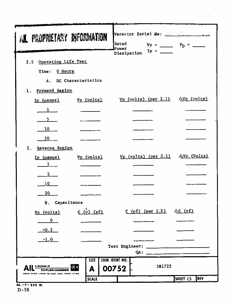
4l P iUA ( O M O aractor Serial N __o:_
Rated Vp = PDPowerDissipation =
2.5 Operating Life Test
Time: 0 Hours
A. DC Characteristics
.1. Forward Region
IP (Pamps) Vp (volts) Vp (volts) (per 2.1) AVp (volts)
1
5
10
20
2. Reverse Region
Ip (pamps) Vp (volts) Vp (volts) (per 2.1) Ap (Volts)
1
5
10
20
B. Capacitance
Vp (volts) C (v) (pf) C (pf) (per 2.2) AC (pf)
0
+0.2
-1.0
Test Engineer:QA:
SIZE CODE IDENT NO.
AIL' CU T LE.HAMM E A 00752 - 38722DjUR PARR. LOne ISLA&ND. NW VOMK 117301
SCALE SHEET 15 REVAIL-F- 335 RI
D-16
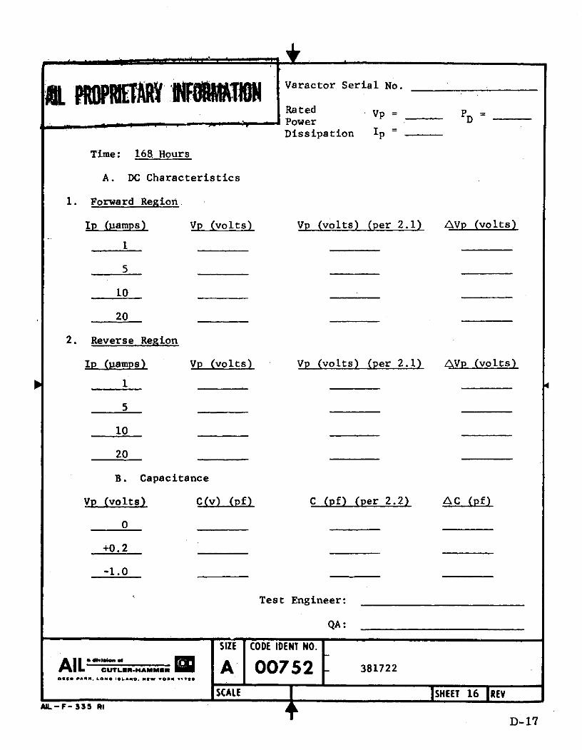
*W PIWP~LFARRY 1~~ Varactor Serial No.
SRated Vp .= PPower DDissipation Ip =
Time: 168 Hours
A. DC Characteristics
1. Forward Region.
Ip (Mamps) Vp (volts) Vp (volts) (per 2.1) AVp (volts)
i1
5
10
20
2. Reverse Region
Ip (pamps) Vp (vos) (volts) Vp (volts) (per 2.1) AVp (volts)
1
5
10
20
B. Capacitance
Vp (volts) C(v) (pf) C (pf) (per 2.2) AC (pf)
+0.2
-1.0
Test Engineer:
QA:
SIZE CODE IDENT NO.
AILO ZmR-AMM E MA 00752 381722Dm PARK. LOe ILAND. NIW 'O0W 1 71eo
SCALE mSHEET 16 REVAL -F- 335 lI
D-17
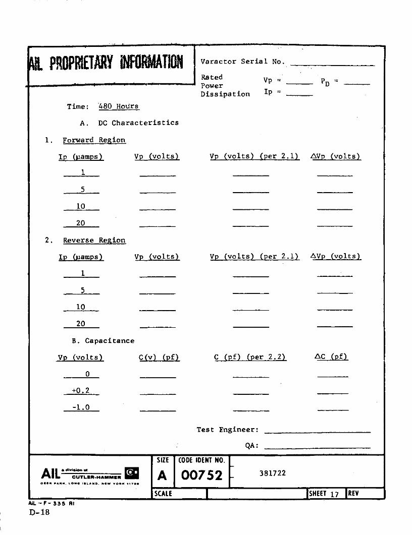
t PROPETARY INORMATION Varactor Serial No.
Rated Vp = ___ "_ Power D
Dissipation Ip =
Time: 480 Hours
A. DC Characteristics
1. Forward Region
Ip (pamps) Vp (volts) Vp (volts) (per 2.1) AVp (volts)
1
5
10
20
2. Reverse Region
IP (pamps) Vp (volts) Vp (volts) (per 2.1) AVp (volts)
1
5
10
20
B. Capacitance
Vp (volts) C(v) (pf) C (pf) (per 2.2) AC (pf)
0
+0.2
-1.0
Test Engineer:
QA:
SIZE CODE IDENT NO.
AIL L. A 00752 3817220 6 0 P A R . L O N G IS L A N D . N O W Y O RM ,1 9 Z g8
SCALE ISHEET 17 REV
DAL-F-335 RI
D-18
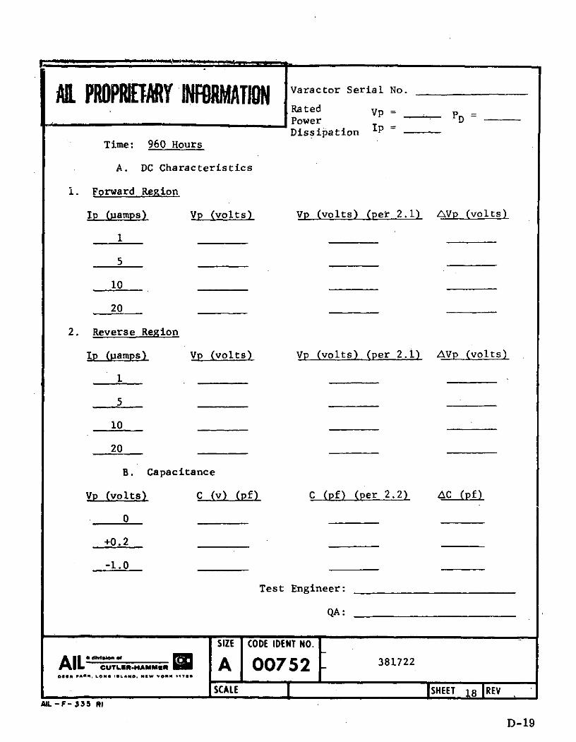
Al IROPRPET Y INtRMATION Varactor Serial No.
Ra ted Vp = PPower D Dissipation Ip =
Time: 960 Hours
A. DC Characteristics
i. Forward Region
Ip (pamps) Vp (volts) Vp (volts) (per 2.1) AVp (volts)
5
10
20
2. Reverse Region
Ip (pamps) Vp (volts) Vp (volts) (per 2.1) AVp (volts)
5
10
20
B. Capacitance
Vp (volts) C (v) (pf) C (pf) (per 2.2) AC (pf)
0
+0.2
-1.0
Test Engineer:
QA:
SIZE CODE IDENT NO.
AIL" CU T LERR... .. E A 00752 3817220D I P A R~ L O N e I S L A N D . N W .YO M N 77 8
SCALE SHEET 18 REVAL-F- 3S5 RI
D-19
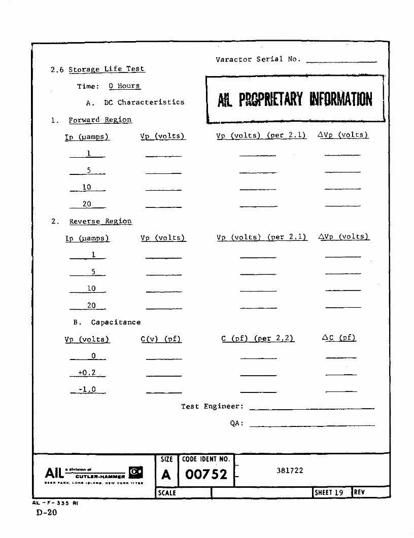
Varactor Serial No.
2.6 Storage Life Test
Time: 0 Hours
A. DC Characteristics A PO MT Y NI A
1. Forward Region I . .. . . ..
Ip (pamps) Vp (volts) Vp (volts) (per 2.1) AVp (volts)
5
10
20
2. Reverse Region
Ip (pamps) Vp (volts) Vp (volts) (per 2.1) AVp (volts)
1
5
10
20
B. Capacitance
Vp (volts) C(v) (pf) C (pf) (per 2.2) AC (pf)
0
+0.2
-1.0
Test Engineer:
QA :
SIZE CODE IDENT NO.
AIL C "U!LZft..SlAMM A 00752 381722Dl2 PAMM, LO*S ILI4O. 16W wor, 1197*
SCALE ISHEET 19 REVAlL-F- 335 RI
D-20
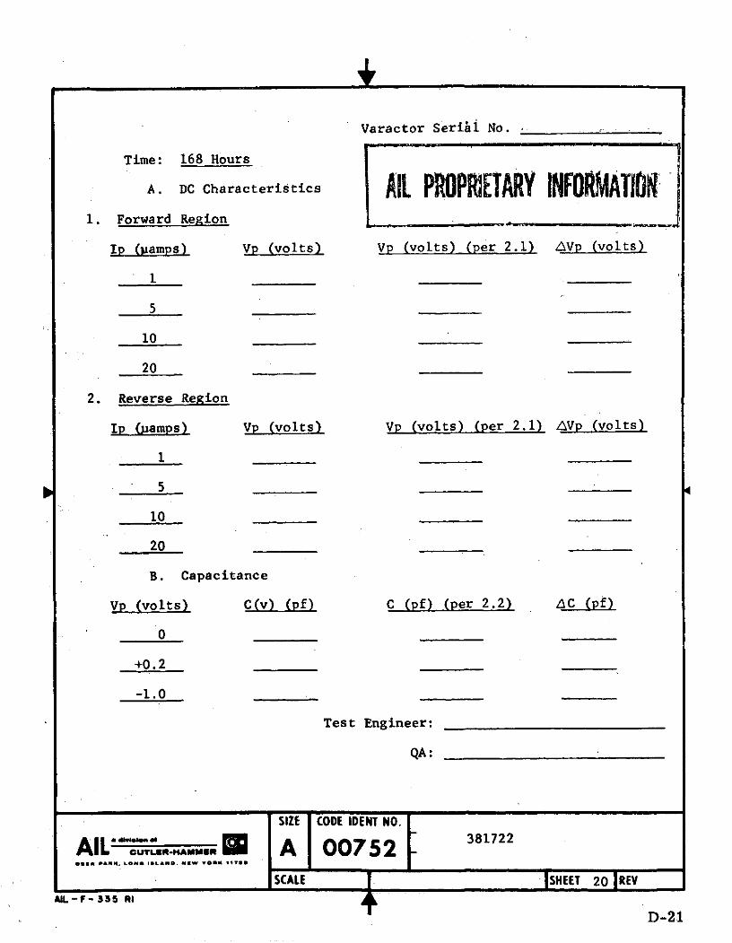
Varactor Serihi No.
Time: 168 Hours
A. DC Characteristics All PROPIETARY INFORMATION1. Forward Region ..
Ip (pamps) Vp (volts) Vp (volts) (per 2.1) AVp (volts)
i
5
10
20
2. Reverse Region
Ip (,uamps) Vp (volts Vp (volts) (per 2.1) AVp (volts)
1010
20
B. Capacitance
Vp (volts) C(v) (pf) C (pf) (per 2.2) LC (pf)
0
+0.2
-1.0
Test Engineer:
QA:
SIZE CODE IDENT NO.
AIL .. ,.-HAMMR A 00752 381722Daga PARK. LONG ILAND, NSW voen 1V9
SCALE I ASHEET 20 REVAL-F- 335 RI
D-21
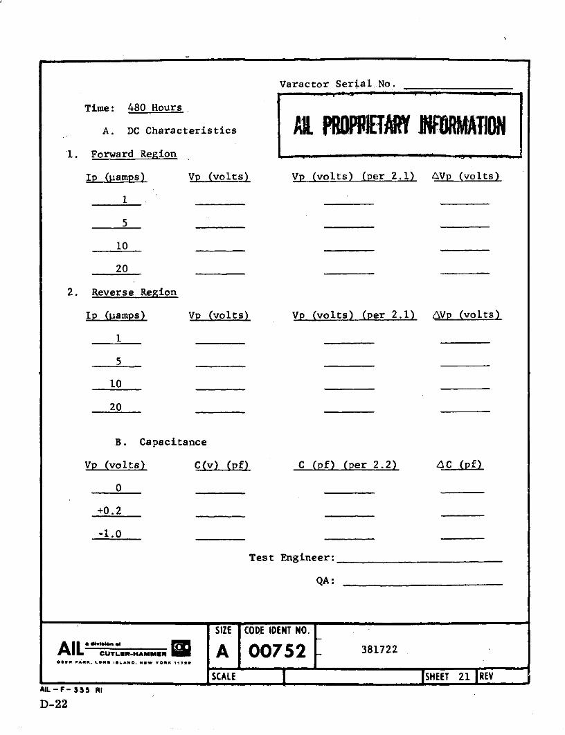
Varactor Serial No.
Time: 480 Hours
A. DC Characteristics Al PROPPIETAW WORM ATIO1. Forward Region
Ip (pamps) Vp (volts) Vp (volts) (per 2.1) AVp (volts)
5
10
20
2. Reverse Region
Ip (pamps) Vp (volts) Vp (volts) (per 2.1) ,Vp (volts)
1
5
10
20
B. Capacitance
Vp (volts) C(v) (pf) C (pf) (per 2.2) 6C (pf)
0
+0.2
-1.0
Test Engineer:
QA:
SIZE CODE IDENT NO.Al'I"VISionoAIL CUTLET~: .- AM A 00752 381722DE0 PARM. LONS iSLADS NEW YORK 11790
SCALE SHEET 21 REV
AlL-F- 335 RI
D-22
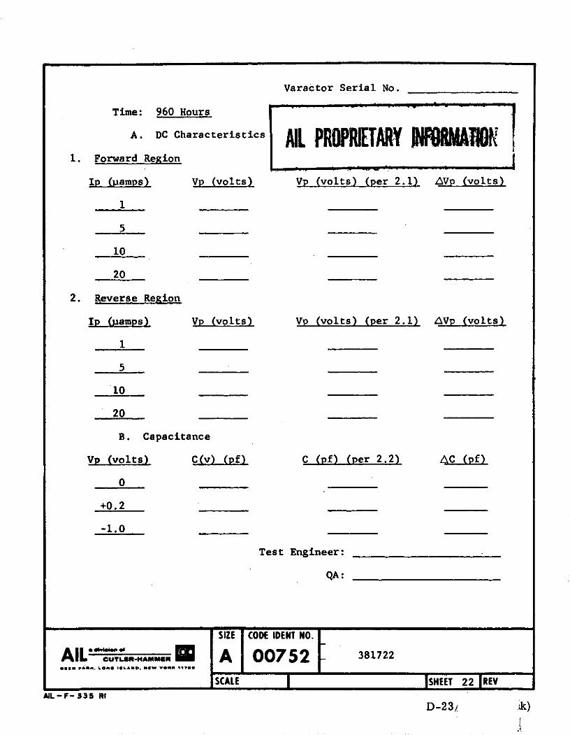
Varactor Serial No.
Time: 960 Hours
A. DC Characteristics A PRO ETARY TOt1. Forward Region R
Ip (pamps) Vp (volts) Vp (volts) (per 2.1) LVp (volts)
5
10
20
2. Reverse Region
Ip (1amps) Vp (volts) Vp (volts) (per 2.1) AVp (volts)
1
5
10
20
B. Capacitance
Vp (volts) C(v) (pf) C (pf) (per 2.2) AC (pf)
+0.2
-1.0
Test Engineer:
QA :
SIZE CODE IDENT NO.
AIL CUTLER-HAME.. A 00752 381722OmEgm PAM. LONo ISLANGD MNW ORNN 1173T
SCALE I SHEET 22 REVAL-F- 5335 I
D-23/ k)
E-1
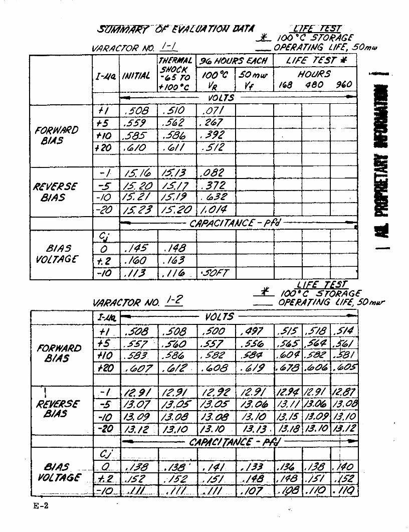
# /00 ' C STORAGEVARACTOR ANO. OPERAT//AG LZ/FE, SOmw
THRALR L 96 HOURS EACH L/FE TEST F
I-4 ///T/AL -5 r 00 OC SO 5ur HOUARS bU*-.
+ /00 oC IR Yf /68 480 960-VOLTS
/ ,508 .5/o .07/
FOR .ARD 6 ,2 _ , -
FO84ARD t .585 . 92.20 ,4/0 - // . 512
-1 /./6 /-;/3 . 82RVEr SE -5 / 20 //.17 .372
8/AS -/o /.. 2/ /.5/9 . 632?f-20 /5 / 201 / 0/
CA C/TAA/CE - P o' -,
8/4S o ,/5 ./48 -
VOLTAG i . _ .160_ ./0-/o .//3 ./(, * OFT
L/FE TEST. /O0* C STORAGEVAPACTOR O. 2 OPE'R,4//G 1/FE, 5 O ar
- - VOL TSS+/.. o8 .508 ,500 ,497 .5/5, .-154
FORWARD S* .5547 .50 .557 .55 , 55 , ~
/4 7210 . 17 . 098 .. 6 - .5&-g 8/
1-/ /R 9/ /29/ / 9 t /2. /291/49// A87REVERS -5" /.3, 7 /; 9, 3. 05 /3 O /OS // /3 /3, 0
8/AS -/0 /36 o9 /.c9 /. 8 1. /o /J. /5 /. /j. /o-zO /./t2 /./ /3.00 /.0 /3/3. , /3/J ./ /1/2
= . .. o€ , CAPAC/ N/C - P, / *
/ ........ ,/8 ./ " ,/ /. , / ,/ ,/-1. I/oVOLTAGE 2 ..ze ./.. / ,/i, /_ ./_/ .. _
S, .. /// .. / ..... 071. / .//o . /E-2
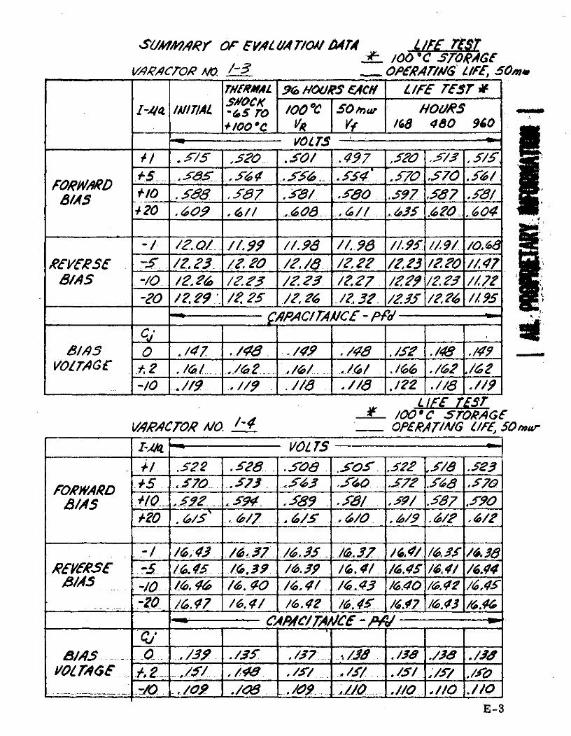
SlkM ARY OF EVAZL r/O A474 LI/CES/oo C Si ORAGE
VARACOR A. /-3 OPRAT/I/G LI/IFE, 50m
THRMA4L 96 HOURS EACH L IF TiEST WSMOCK
Z-44 IA/IT/AL -, ro /O0 C 50 mw HOULRSS/oo * O VR Y 1 /68 480 960
VOLT "/ . 5-5 .20 .50/ .497 -41 ./3 . /_-
f5 . £45 . £€ . .€ . £.4 .£0 ,570 1. /8/AS / ,8 ,587 .89/ .sO8 . ,587 f8/
_20 /aI9 .//8 .1/ .&5 .0 .404
-/.0/ . . //. //.8 //. //90.REVR.SE~~- . .23./. 20 /./ / /. 22 /223 / /ZO // 47
/AS -/0 /2 2 .2?3 /2.2 A, .27 /e f /2. /7-20 /.2. /2 / / 74 /?32 , /! /224 /195
SPAPC/TAA/CE - PFd
8/AS 0 ./47 ./8 /9 ./ ./5 ./48 ./49 __
VOlTAG(E . . /, /2. ,/6 / ./~ I./2 ./62_ -/o0 .1/9 ,//. ./8 [/8 .122 .//8 .19
LIFE TESTS/00 5C STORAGE
V4PAACTOR AO /'4 OP4ERAT/AIG 1/F1, 50omr
_-,_ 141- VOL 75 _
1. . .52. . 28 . 50 ,0522 .5". ,/8 .523R 5S .. 57 . 523 . ~34 .0 .72 . f8 ,570
ARDS 5. .589 . / -/ .587 .590-20 .61/5 .6 -' e/O . 449 .6/? 14/
-. / A A /6.57 /. . /6.7 / . / /4/ " /.38REVERSE .- 5 /.... 45. / .39 /6.9 16. 4/ /6.45 /6.4/ /6.44
_O - /. 7 /6.0 / /6. 1 .6...4 1/~7 /6.43 /.46
- - CAPAC/rA /C-P '
8/AS4 5 .- .39 ./5 ..../7 .. d .... ./38 ./38
_ -/0. .. /0 ./ . / . LO ./ .//. 0 .// O
E-3
/,S4MA. OF EV4L /A TI/OAI 4TA 474E TST)-K- /00 0 C SrOAGE
VRACTOR ANO. 1-5 OP6RAA/6 L/F, 50EmoIT//AMAL 9r HOURS A4C// LIFE TESTSMOCK
-/44 IA//7IAL -I5 rT /00 *C SO/ HOURS1*/o °C I .VR VI /08 480 960
I a_ 'VOLT 75 _-
/ .5?4 ,5 .5081. .o .5/8 .5?Ze .5S/R 5 . ..578 .58 .577 . 58 ."9"
8/AS 0 ,07 . 0.9 ,584 .85 . ! r90 .5820- . /6 . .1/ /S .- / .1//. .6-/3
-/ /3.39 /f. 35 /3.33 /3, 34 /3.38 /3.34 /3.35REVERSE -5 /Jr 5 f. 05 /3.40 /3.4/ / 45 ./3,4t 144
8/AS -/0 /3. 47 /3.49 /3. 42 /3. 44 / .6 4'1 /3.45-20 ./- /35 /34 /3 fe /3f,49 / 45 /3.
C - CAPAC/TAA/CE - PPd
81,4s O ./9 ./9 ./4 ,/5<6 ./3 ./37 ./38VOLTAG I 2 . 15/ . 5 . )8 .. / 1.5/ ./5/ /50 /5/
. -/o . //2 . / ....... o// /,1/ . /// . i/2L IFE TiST
00 /0 C ;TORAGVAPA4COR A. /- M OPERAT77IG L/FE, 50mir
~-kP~F---------- Vol0 75
+1 .528 . 3/ .5/3 .. 0 ..5 .54 .5o5
FORWARD .5 .574 .577 ..566 .X0 .5-7 .57/ .470B/5-AS .. I/0 6-P .. 99 .I ,87 . 9o , 592 ,.5j
-/..... . 3 /., /3 / 6. 8 7. 40 /6,45 / ,43 /6-.REVERSE -5 / ' /. .. /6.42 /6... /.4.. 4 /~.i.44
-/0 i/6. 48 / .43 1.44 /C .41 ,99 16,45 /6.472.O .. 1/.50 /&6.4 14 /.48 /6.5/ /6.47 /1.49
__-____ _ CAPAC/ 4A/CE - P /"J. _. _' _ _
8/45 O .//47 ./3 ./ ./g *//2 .1/3 .//3VOl7 _ 2 .25 ./ .2120 . I4 .1 .14 .le3
.-/0 .090 ,.V90 . ... .. / . I08 .O ; o8E-4
.L /00 C STO7RAGEVRAACTOR ANO. /-Z OPERAATA/G L/FE, 5Oeu
WERf/MAL 96 HOURS 4CH LIFE TEST *SHOCK 'A 5 ro j00 C SO mr, HOURS
+00 oc 1L V Y /68 480 960VOLTS ...5_ ,
i / .508 ,5/0 ,95 '488 .505 .508 .507+5 .555 .557 ,549 ,544 .A43 .?9 .55/
57 7 .575 .557 ,575 .J.74 ;57f8/20 . 00 .603 , 00 ~ 596 .595 ,6 00 .599
/ . / S /2./9 0/2 /8 / // / O/00REVES -5 /7 /. .4 ,3 / / 7 1Z49 / 14
8/AS -/O /0 5/ / ~ / 4 .i , . /5s~ /, 7 // Fo-FO //5t /. 5/ / ..52 /252 /7.54 / A .5
-___ CAPACITANCE - PPo' .
B/AS O ./d -,/d ./> .i8_ . .187 ./9O ./d8VOLTAG( +.2 .20 . F . 2o 1 .207 ./2 1., 0
-_o .-/0 ,45" ./4 ,. / . /3 ./€." , /5O ./€
/Co 0C STORAGEVARACTOR A/O. /-8 OPERAT//6 (/FE, 5Oru-~A t VOLTS 7s
+ .. 5/6/ , 523 .505 .4197 . O
.FOAR1, S 515 . . 6f .558 ,552 PFORWARD8/AS 1 ..85 .859 .I.9 .. 578
.20 ./0o ..../2 ./ .6~ A)
-, / .... i'37 /,.. /3. 20 / . ,R~EVERSE -5.. /. 97.. /59_ /.3 .. /8 . _ "
0/-0 /. f I/3.P7 //0 /3 4.3C'APC/TAA/CE - P V
8/,4 ..... - 4.... , 1 8....:. . ..... ,1 7 .... . . ..VOL T/ . . .157 .55 ,152
- . .7 . o L
E-5
//diwAR c" FVA4L A1/4 T/ON/ 44T L/FE TST7S/00 a C 57TOAGE
VARACTOR AO. /-9 OPERATMA/G L/F 50 on
TiERMAL 96 //OURS EACH LIFE TEST w
1-44 I//TIAL -05 ro /001 C 50 m HOURS+0oo'c v. V, /68 48o 9o60
/ / 5/7 ,.5/.9 .501 .499 .4// .R 2 .513O' 5 .5 4 .565 .556 .'54 .. o 0 .547 .5(43
FORWO4D o8 A ,./O... . d . ,3 . 578 .87 .53 .58420 . L08 . 0 .609 . 04 .403.406 .6o1
-/ /4 5 :40 /5:.7 /.40 /14 / 14//5.4R1V5R-SE -5 / 54 /52' /IS / / 4 / 47/ 5. /5 45
8/AS -/o /5. 47 /:. - 3 /5:. 4 /. 4 /5 8 /. 8 44 I546-,o... /. .. / 4 / S /S. 47 11i... /.45 /r46
CAIPAC/TAACE - pPd
0/3 /s ./5.5 ./5 .15/ . / ./15 ./55 ./VO TA4C . ./73J .0 ./67 ./73 .1/72 .170 .70
...... -/0 . /22 ./20 ./7 .12 O ./? ./20
S/00 C STORAGEVARACTOR /AO. /-/0 OPERAT/A/G (/FE, 50 mr
Z-IA4 " VOL TS/ .2,7 .528 .. /o .52 .5 .5t3 ..5
FOAR . 575 .-5:78 .- 4 . /I ..50 .572 .574FORWARD -H, S.9,1/AS .5 ....9/ .. 88 3, .59/ .598
20 , 9 , 4 .6/ I ., .4
. -.. ,,3 /,. .3 /. 3/ /,.37 /4.1O /.55 /6.37REVE'RSE... -5 /',38 /,35 /, 15 /, 9 /.,4/ /6.37 16,o1// 6, 9 /1,34 /6.37 /6, /6A la.41 69 P. /
___ ___ ______ CAPAC/T44/CE - ___
8/43 -~G'- -- I7 /F 74 //.7 //VOLS............... .i....... /4O . . i/ 0.. ./ .... 1/31/ . ,/ / .
-/0 .1, ., 30 ./.o (01.00 1/6D .4,A 5f
E-6
JS/MiA4RY O EVL Z/AL4 TO/dR /rF Tt/00 'C 5TORAGE
VARA4CT;OR NO. 3f/ OPLEAT/4 LIFE, 50,md
THEfRMAL .99 HOURS CCH L/FE TfEST
1-/ IA1175AL " To /O0 C 50o HOURS+/oo *c VR /68 480 90
VOSL 5/ .524 .525 .507 .507 _
R 5 .572 . .5/ .559 O/ A ../0 . ..9593 .587 ,584 F.
A 20 ., . .. / . /3 " -// 7
-/ /8.o02 /8.o /7. 96 /8.0/
REVESE -5 /8. o0 /8.03 /. 02 /8.o 0(8/AS -/O 18.07 /8.04 /8. O84 /8.08
-..0..0 /8.09 /8.05 1/8.06 /8. 09
CAPACfTAA/CE - P_CI'8/A 0 .1/7 .//1.9 .3. ./9
VOZ7TAG,4. Z ./128 .13/ .152 .130-/o . 097 .095 .1/5 .094
L /,F TEST/00 C SFORAGE
VA4ACroR A/o 3-2 ..... OPERAA1/MG l/ EO SOm,
one_ VOL TS+/ .528 . 533 .5// .509 .SS .573 .576 .5~47 .5 3 o
FORWARD/AS4 /O . 597 .598 .593 .~57 F7
,20 . 20 . 22 ../9 , I/5 T
- /7. /7.93 /7.90 /Z795REVE6SE -5 ./. 97 7 /I94 /7.9, /7 98
As -/ /Z 98 T/ 795 /7 95 /7. 99-O. - /7 99. /79 /79 /8.0/
/- AC/74cA//CE - E -
8/ 0... 0 ,// . /108 .//0 . //VOLT4gE - 9.2 ... / .//9 . // /./ . .. ...
..- /0 .088 085 .087 .068E-7
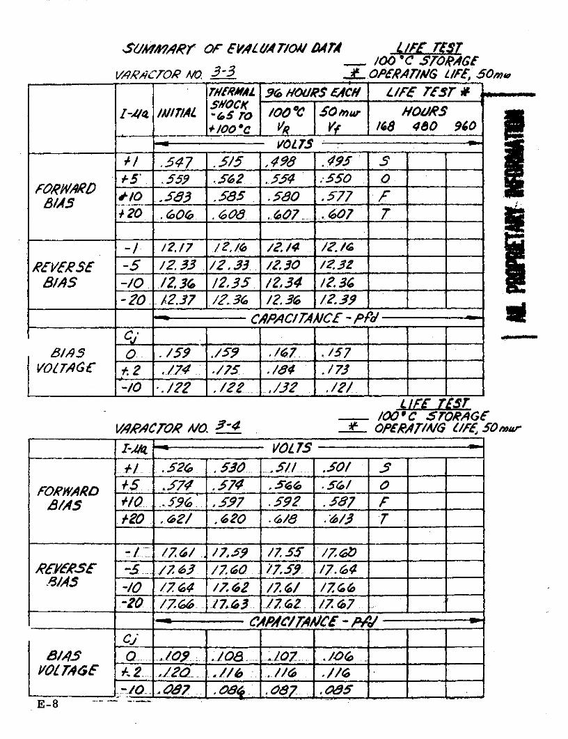
A//A4R- OF EV1 A T/OA/ 4TA L iFE TA EiS/00 ' C STORAGE
V4ARCeOR NO. 3-3 .. .OPERAT/A/ L/F, 5OmwT//RMANL 96 HOUR#IRS E5C LIFE TEST ,SMOCK
Z-44 IA/ITIAL -&5 ro /OO 0C 50 mw HOURS/0oo0 V / 168 480 960
VOL TS/ .547 .5/5 ,498 .495 s ",
, 5 .559 ....5 -2 . 554 .550 O/S4R / 0 583 .585 .580 577 F
+ 2o . 606.. 608 .... 07 .407 7
-/ /2,/7 1/./6 /2.14 /Z./6
yEVERSE -5 /2.33 /2.335 /.30 /3ZB/AS -/0 /2.37 /I2 6 /2.36 / 4 2.3
-20 /2.37 /.35 /2.34 /2.3. 1-'...CAPACTAA/CE - Pd "Pd
B1/3 O.. . /59 ./5 /67.. 57VO/TAGf +. 2 .174 . 75 .184 ./73
-/o ./22 ./2 ./32 ./2LIrS" TES
/00 C STORAGEVAWIACTOR A/O. 34 OPIERATI/AG IFE, 50m,-
r-/ VOLOL 7_
+/ .526 ,530 .5// .50/ __
.FOAR -. . .57 574 .7. .5 o .56/ 0-AS / .9 , 97 . 592 .587 F
720 ,62/1 .620 . /8 ., 7
R5VER6.sE -5 /2 /7. 0 Z7.S. /7.64/1S -/0 / 764 17. 2 /7. / /Z 66
.- 7o /76 /7603 1762 /.Z .7...,_-m CAPCI/ /CCE - y __ ._
8/3 o ...... .... ./. .o.ro ... 1,/06 .VOLT G A 2 2 /..... . 6 .e ..1 .// __
-1o._ 0 7.. o . 09 087 . o*9E-8
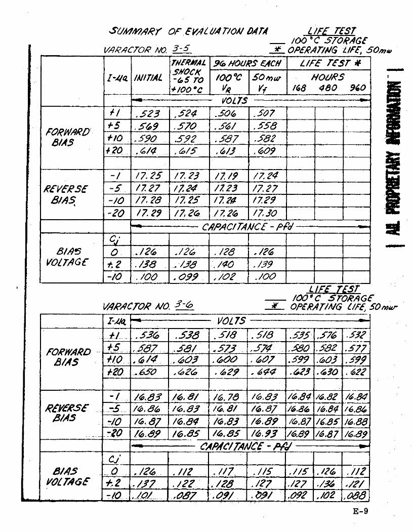
/OA1/,/A4Rr OF EV4AL 6/4 TIONA DTA L /FE TEST- /00 ' C S7ORAGE
V/AR'4TOR , M. 3-5 ' OPAERAT/,G LIFE, 50owTI/IRMAL 96 HOURS C/f L /FE TEST rwS'//OCK "'
I- IA/I/AL -65 To /00 0 C 50 m w HOURS+/0 C Vo R YI /8 480 960
=__ __ VOLTS .. ..-
'/ .523 ,524 .50 .507 .7
-5 .569 .570 .56/ .8 _8
FORWLARD.8/AS I-0 .590 .592 587 -582
20 ....614,... ./3 ... 609
-/ /7.25 /7.23 /7/9 /7 Z24
REVERSE -5 1727 /724 /1723 /7. 27/AS -/o /7. 28 /7 25 /7 2 /729
-20 /7. 29 7,O, / 26 /7 OCAPAC/TAA//'-CEd - P,'
8/AS O .. 12 .126 ./28 , /VOZLTA '. 2 ./38 . J ./0O ./ 39
-/O ./00 O 099 ,/02 ./00L IFE TEST
/00 C STORAGE"W/A CTOR NO/. -- OPERAT/MG /F, 50, wr-~ z"- voLrs -- - =--
__ _zt _VOL 75 _
1 ... 3 .538 .5/8 .5/8 ..55 .576 -53
FOAWAARD 5. .587 .58/ .573 7 , 0 , 52 .5778,/AS 0 4 . .0 0 . 7 59 .~ 03 5.9~9
,20 .650 ,. , 6 .64 .630 .622
- . /~.8 /. 8/ / 78 /6.83 /6.84 /-.82 /.w84RVERE -. .8 /.1 /6. 8/ /. 87 /.86 /6.84 /1.84
BS -0 /. 87 /6,.84 /1~83 /6.89 /6.87 /.85 /.88-O.. /16. /6.85 /4.85 /6s.9 /6.89 /6.87 /6.89
- CAPC/7A/TAICE -P/V -
8/4S -. /26 . // .//7 .1/5 1//5 ./ .//VOLTE AG. 2 ./ 7 ./21 ./28 ./27 ./27 , / I/
-_o._ ,J . /_...... ,'07 , I.. g9 l/ .92 ,/2 ".E
E-9
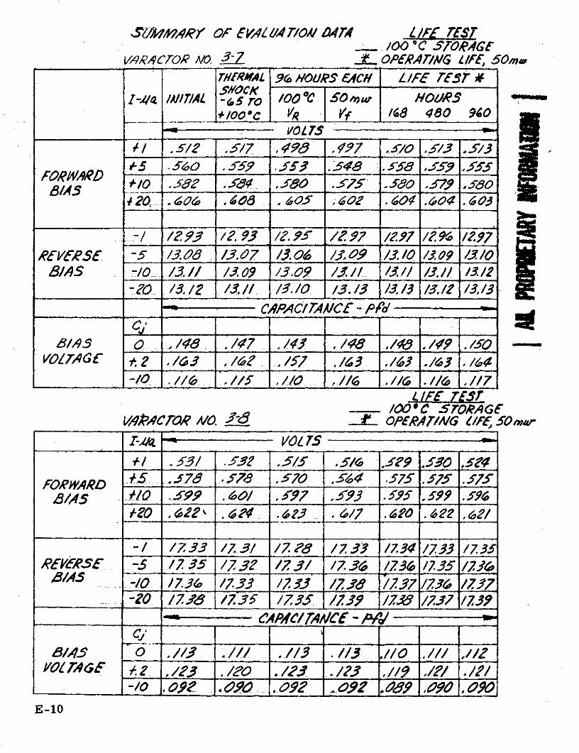
4'I(MAR OF VAZL dA T/OA/ A44T L /F TET/00 °C SOAGE
V/ARCroR NO. A/t OPERAT/NG L/FE 50muTHE7AL 9ro H/OURS EACH L FE TEST AS/lOCK
Z-44 IA/IT/AL -o5 To /O0 C 50 ,SOw HOL/RS/00 oo*C VIf /68 480 940VOL7TS
/ .512 .5/7 ,498 . "7 .O , ~3 5/3
I0/O .59? ,-58. ,580 .s75 5c90 .79 ,57
_ 606 . 608_0 _ ao 00 . /0.04 1_603
.-/ 1. /2 9. /2.9 /M97 /297 A?9 /1297
RYERSE -5 /3. 08 /3.7 /306 /,9 /3./O /o9 /.3/o/AS - /3.// / .o9 /3.9 / .// /..// 3/3/2
,-O /3.12 /.// /3./0 /3.13 /3.13 /./1 /3,/3
CAPAC/TAAC,/C'P - PA Y
8/MS o.. /8 ./47 ./8 . /O ,/ f ,/4P ./O -V/ 7AGE F. 32 /3 ,, 157 . /3 .163 ./63, .64
1.F 1-/0 /F // I // / // , // .1 /C ,//7LI E TOT
/00 C ~S .TORAG FV,4ACOR NO. 8 . OPERAT/NG / /, 50,wu
Z-4a VOL TS .+/ . .9 .5< . /5 4 .5/ .5 . 5f5 . ,7.5
FORWARD _S .78 .578 .570 .5.' .575 .575 .5754BAS i0/ .5.99 .60/ , -97 5,93 ,595 ,,959 .591
20 ,622 .6.3 ., .6/7 .640 .62'2 ,2/
-/ / 33 /7 3/ /7 78 / 7 3 /734 /733 /735RE~VESE -5 /7 35 17,32 /73/ /7.3 /Z3 /735 /7Y,
B/AS -10 /7.36 /733 /7 51 /7Z /737 /73, /7. 7.. 20 /78 /Z 335 /Z 7, /7j. /Zd /737 /739
CAP /TAAI/CE - P -_/
8/4 o .//3 /// ..//3 .//3 j .// //zVOLTAGE .. ,/23 ./O •/2 . 123 ,II ,/2 .12
S-/0 .092 0..... 09 , ,09 09 ,09 90
E-10
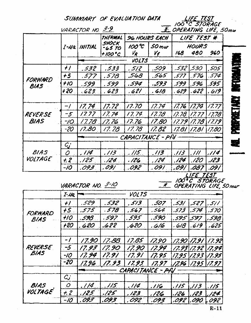
S6'/MAIARY OF EV,/L 4TO/ 1 DATA L/FE TEST- /00 ' C STO7AGE
V/ARAACTrR /VO. -9 .L OPERATI/AG LIFE, 0OmwT//RMAL 96 H/OURS E4CH L/FE TEST rSHOCK
Z-n IA/HIT/AL -,5 ro /00 C SOur HOUR S+/oo *c V 1 /68 480 940
VOL 7 3 _
_3/ .532 .533 .5/? .509 .32 .530 50515 .577 , 578 .5o8 .56 5 ,577 -f7; .574
FORIV//RDO8/AS /A o 59 .99 .59 59. .9 .99 .5% .5958 /A . 23 . 423 .41/ . 4/8 6 ..422 .c /9 --/ /Z 74 /7 72 /7.70 77 /77 /774 /Z 77
REVESE -5 .. 777 /7Z 74 77 74 178 /778 /777 /7788/AS ./0 /Z7Z8 ./Z_ 7.7~ 7. 0 /79 ./Z78 17.79
-?O /7,0.. /Z /77./Z7 78 78/ /8/ /7,80_____ _CAPAC/TAA/CE - Pfd' "
81./AS . //. ./3 1 f .//3 ./ ./ ,//4 *VO TAG" . 2 ./25. ./21 _/__ / /,4 ./20 ,/3 -
,_o .-/0 . . . ., / . o09 ... 09/_ ,, .. .09/L IFE TEST
/OO C STORAGEV4ARACTOR MO. -±-I' OPERAT/A/G 1/FE, SOmr-- L - VOL 7S+. .59 . 2 . 73 .57 .53/ .54?7 ,5//
FOAWARD 5 . 75 .78 .567 .5 573 .57I .570
B/AS -/0.58 .5 97 .. 3 .90 . 97 ,P8O 2 ,20_ .1.... 122 .20 . &4 -4/8 '1/9 L 2
-/ /790 /7,<8 /7,68 /,90 17/90 /.9/ /7.92RIVE, SE -5 /7. 9- /7 90 /7Z O /, / /79 ?2 / 7,99
B/AS - /Z 9# /9/ /7 91 /7 95 /Z75 /)93 1720./ /3 /~/ 97 /7?P / 95 I/.97
_ CAPAC/TAr/CE - N/ .
/I4 , . /... 4 .1/.. .... . / . /5 .1/3 /
-7/0 . FOQ 3j OP3 .... ; .. , 00 092E-ll
a division of
CUTLER-HAMMER SPEC NO. 00752- ENV-72-2DEER PARK, LONG ISLAND, NEW YORK 11729 CODE ;NO.RE
RANDOM VIBRATION TEST REPORT
ON
C.R.G. VARACTOR DIODE
PREPARED BY: DATE: 2-14-72C/ H. Grum
E-12 PAGE 1
AlL F,,66 E1
SPEC NO. 00752- ENV-72-2CODE NO. REV.
TABLE OF CONTENTIS
PAGE
1.0 SCOPE 3
2.0 APPLICABLE DOCUMENTS 3
3.0 TEST CONDITIONS 3
4.0 SEQUENCE OF TESTS 3
5.0 TEST PROCEDURE 4
- 6.0 RESULTS 6
APPENDIX A - PHOTOGRAPHS OF g /cps Vs. Channel No.
PAGE 2 E-13
AIL F ,M 12
SPEC NO. 00752- ENV-72-2 DCODE NO. REV.
1.0 SCOPE
This document defines the Vibration testing performed on four
C.R.G. Varactor Diodes at A.I.L.
2.0 APPLICABLE DOCUMENTS
The document listed below forms a part of this report.
Document No. Title
MIL-STD-810B Notice I Environmental Test Methods
3.0 TEST CONDITIONS
Unless otherwise specified the vibration testing was conducted at am-
bient temperature 750F in the X axis, 1020F in the Z axis, and ambient
pressure of 760 mm of Hg.
3.1 Test Equipment Calibration
All equipment used for testing had been calibrated. All equipment
used for testing exhibited calibration labels stating date of last
calibration, date of next calibration and property number.
4.0 SEQUENCE OF TESTS
4.1 Random vibration X & Y axis at 5.4 to 16.0 gras.
4.2 Electrical check.
4.3 Random vibration Z axis 5.4 to 46.4 grins.
4.4 Random vibration X axis 20.7 to 46.4 grms.
4.5 Electrical check.
E-14 PAGE
MIL F-3A 12
SPEC NO. 00752- ENV-72-2 DCODE NO. REV.
5.0 TEST PROCEDURE
5.1 Vibration Equipment Used
a. Vibration Exciter MB Electronics, Model C60.
b. Power Amplifier, MB Electronics, Model T452-B
c. Equalization Console, MB Electronics, Model T485
d. Spectrum Analyzer, MB Electronics, Model T491
e. Accelerometer, MB Electronics, Model 302
f. Oscilloscope, Tektronics, Model 535A
g. Accelerometer Amplifier, Unholtz, Model 8PMCVA
h. Camera, Dumont, Model 2614
i. Automatic Exciter Control, MB Electronics, Model N575/N576
j. True R.M.S. Meter, MB Electronics, Model N120
5.2 Test Setup
5.2.1 X&Y Axis
The four diodes were placed symmetrically on a 1i inch thick
aluminum plate 7 inches in diameter. This plate was attached to the
horizontal slip plate. The slip plate was floated on an oil film
table. The input was colinear to the X axis. One accelerometer was
oriented to detect vibration in the same axis.
5.2.2 Z Axis
For this axis the aluminum plate was bolted directly to
the moving element of the shaker.
PAGE E-15
AIL F-39 I2
SPEC NO. 00752- ENV-72-2 OCODE NO. REV.
5.3 Random Vibration Equalization
With the accelerometer attached to the vibration fixture
but without the diodes the exciter fixture was equalized via
the Spectrum Analyzer and Random Console to the following power
spectral densities which was test curve AE of MIL-STD-810B.
20 to 100 cps at 6 db per octave roll on
100 to 1000 cps at .02 g2/cps
1000 to 2000 cps at 6 db per octave roll off.
This energy had a overall of 5.4 grms. The on-the-line Spectrum
Analyzer together with the rms meters monitored the acceloerometer.
None of the 48 DC level energy had less than 50 cps bandwidth. When
the system was equalized the levels were brought to zero and the 4-diodes on the fixture were mounted.
5.4 Random Vibration Test
5.4.1 Paragraph 5.3 was repeated with the diodes in place according
to the following:
rest Curve Spectral Density Gras Time (xin) Axis
AB 0.02 5.4 3 X & Y
AF 0.04 7.6 3 X & Y
AG 0.06 9.3 3 X & Y
AH 0.10 12.0 3 X & Y
AJ 0.20 16.9 3 X & Y
E-16 PAGE
AlL F-$G It+
SPEC NO. 00752 - ENV-72-2 ICODE NO.
rest Curve Spectral Density . Grs Time (min.) AXis
AE 0.02 5.4 3 Z
AP 0.04 7.6 3 Z
AG 0.06 9.3 3 Z
AH 0.10 12.0 3 Z
AJ 0.20 16.9 3 Z
AK 0.30 20.7 3 Z
AL 0.40 23.9 3 Z
AM 0.60 29.3 3 Z
AN 1.00 37.9 3 Z
AP 1.50 46.4 30 Z
AK 0.30 20.7 3 X.& Y
AL 0.40 23.0 3 X & Y
AM 0.60 29.3 3 X& Y
AN 1.00 37.9 3 X & Y
AP 1.50 46.4 30 X & Y
6.0 RESULTS
Appendix A contains the on-the-line random vibration data. All
electrical tests were performed by project.
Appendix B contains the electrical test results.
PAGE 6 E-17
AlL F,.8 It
SPEC NO. 00752- ENV-72-2CODE NO. REV
APPENDIX A
The key to the on-the-line Spectrum Analyzer, MB-T491 is the bank of
48 crystal filters resulting in 48 dc voltages displayed on an oscilloscope
indicating proportional g2/cps energy. A complete plot of spectral density
over a 2000 cps band is displayed in each photograph.
Vertical Calibration
The 48 dc voltages are calculated from the photos using millivolt
per ca given times the number of cm shown in the photo. A graph for g2 /cps vs.
voltage then converts voltage to g2 /cps. 4
Horizontal Calibration
Every one of the 48 dc voltage markers is assigned one horizontal
graticule marker.
Channel 1 (12.5 cps) thru 8 (100 cps) are 12.5 cps wide.
Channel 8 (100 cps) thru 25 (200 cps) are 25 cps wide.
Channel 25 (200 cps) thru 48 (2000 cps) are 50 cps wide.
E-18 PAGE Al
AlL Fl30 1A 2
X-Y Axis
Photo Vert. Scale Test Curve
.1 mv/cm AE
.1 mv/cm AF
.1 mv/cm AG
.1 mv/cm AH
.2 mv/cm AJ
.2 mv/cm AK
.2 mv/cm AL
.5 mv/cm AM
.5 mv/cm AN
.5 mv/cm AP
E-19
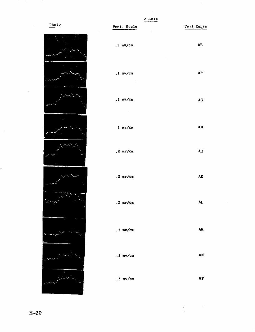
L AXIS
Photo Vert. Scale Test Curve
.1 mv/cm AE
.1 mv/cm AF
.1 mv/cm AG
1 mv/cm AH
.2 mv/cm AJ
.2 mv/cm AK
.2 mv/cm AL
.5 mv/cm AM
.5 mv/cm AN
.5 mv/cm AP
E-20
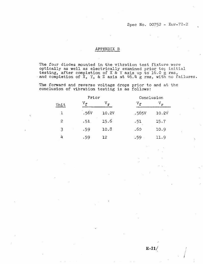
Spec No. 00752 - Env-72-2
APPENDIX B
The four diodes mounted in the vibration test fixture wereoptically as well as electrically examined prior to; initialtesting, after completion of X & Y axis up to 16.0 g rms,and completion of X, Y, & Z axis at 46.4 g rms, with no failures.
The forward and reverse voltage drops prior to and at theconclusion of vibration testing is as follows:
Prior Conclusion
Unit Vf Vr Vf Vr
1 .56v 10.2V .565V 10.2V
2 .51 15.6 .51 15.7
3 .59 10.8 .60 10.9
4 .59 12 .59 11.9
E-21/
APPENDIX FNOISE TRANSFER ANALYSIS--GENERAL CASE FOR
MULTISTAGE PARAMETRIC AMPLIFIER SYSTEM
The analysis in Appendix C was based upon the intefering signalbeing in the passband of the amplifier.
Referring to equation C-8,
APn =K _ nP pni P At
K really represents the gain for the frequency of the interfering signal f
In case K represents the gain in the passband and the interfering signalf is outside the passband, so that the gain at f - f = pK (p < 1), thes5 f) s( f)
general formula should read
A Pin = oK pn P (F-i)p S(Af)
Assume now n cascaded stages with:
Kn = mid-band gain of nth stage
n Kn = gain of nt h stage at f = f
a Pn = noise quantity of the pump of the nt h stageP
p
F-1
The transferred noise to the input of the nt h stage can now be written
as:
Pni N n n P n s (f) NN pn Kn [ n] ( P 5 ) N (F--2)
where the suscript N refers to the fact that those quantities are taken at the
input of the nth stage.
For the noise components falling inside the passband, the noise con-
tribution of the nth stage can be transferred to the input of the first stageaccording to:
P) ni N K r AP 1 (F-3)nn Fn-1 n n 7 s p=n-1
n K p n Kp=l P p=1 P
with:
Fp=n-1
s(af) NL p = 1 P s(f)
it follows:
p=n [7_'_AP ni =T o K n P (F-5)
n n p=1 p n P (f)
F-2F-2
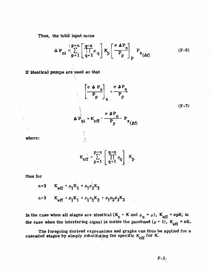
Thus, the total input noise
\p=n =nP =q] F P K[ AP n P (F-6)
ni \= 1 q p s(Af)
If identical pumps are 'used so that
n n
n
(F-7)
a bPAPi =K PSi eff P s('f)
p ()
where:
pK q=n
eff =- pq
thus for
n=2 Keff = P1K1 + P1P2K2
n=3 Keff = p1K1 + olo 2 K2 + olP2p 3 K3
In the case when all stages are identical (Kn = K and pn = p), Keff = npK; in
the case when the interfering signal is inside the passband (p = 1), Keff = nK.
The foregoing derived expressions and graphs can thus be applied for ncascaded stages by simply substituting the specific Keff for K.
F-3


![Horario Abril 2020 - EMILIO VALENZUELA · &rohjlr (plolr 9dohq]xhod &ud %rjrwi-xdq &duorv %hoor $eulo d6f +rudulrv,qj 90 (& /+ 0dw &* (vs &5,qj 90 6rf 35,qj 90 & 1dw && 6rf 35 $uwh](https://img.pdfslide.us/doc/110x75/5f5c8fe268d67d4947799086/horario-abril-2020-emilio-valenzuela-rohjlr-plolr-9dohqxhod-ud-rjrwi-xdq.jpg)


![ABriefIntroductiontoRayTracingand Ionospheric Models · 2018. 2. 23. · potential energy” [Marion and Thorton, 2004] Lagrangian Formulation Z L(qj,q˙j,t)dt =0 L(qj,q˙j,t)=T(˙qj)](https://img.pdfslide.us/doc/110x75/6095fc7435f16d6778597e57/abriefintroductiontoraytracingand-ionospheric-models-2018-2-23-potential-energya.jpg)


![&XUULFXOXP YLWDH 3URI 'U ,QJ $OYDUR *XWLpUUH]](https://img.pdfslide.us/doc/110x75/58a2f8e11a28ab2d678ba55a/xuulfxoxp-ylwdh-3uri-u-qj-oydur-xwlpuuh.jpg)