Embed Size (px)
Citation preview
Journal of Engineering Science and Technology Review 6 (1) (2013) 38-43
Research Article
Voltage Stabilizer Based on SPWM technique Using Microcontroller
K. N. Tarchanidis1,*, J. N. Lygouras2 and P. Botsaris3
1Dept. of Petroleum Engineering, Kavala Institute of Technology, Ag. Loukas - Kavala - Greece
2Dept. of Electrical & Computer Eng., Democritus University of Thrace, Xanthi, TK 67100- Greece 3Dept. Production Eng. and Management, Democritus University of Thrace, Xanthi, TK 67100- Greece
Received 25 June 2012; Accepted 15 January 2013
___________________________________________________________________________________________ Abstract
This paper presents an application of the well known SPWM technique on a voltage stabilizer, using a microcontroller. The stabilizer is AC/DC/AC type. So, the system rectifies the input AC voltage to a suitable DC level and the intelligent control of an embedded microcontroller regulates the pulse width of the output voltage in order to produce through a filter a perfect sinusoidal AC voltage. The control program on the microcontroller has the ability to change the FET transistor firing in order to compensate any input voltage variation. The applied software using the microcontroller’s interrupts managed to achieve concurrency on the running program.
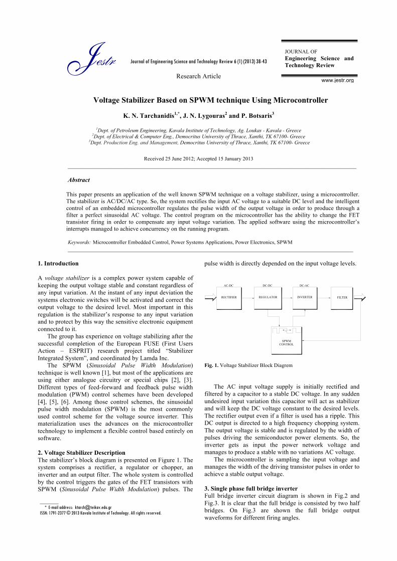
Keywords: Microcontroller Embedded Control, Power Systems Applications, Power Electronics, SPWM __________________________________________________________________________________________ 1. Introduction A voltage stabilizer is a complex power system capable of keeping the output voltage stable and constant regardless of any input variation. At the instant of any input deviation the systems electronic switches will be activated and correct the output voltage to the desired level. Most important in this regulation is the stabilizer’s response to any input variation and to protect by this way the sensitive electronic equipment connected to it. The group has experience on voltage stabilizing after the successful completion of the European FUSE (First Users Action – ESPRIT) research project titled “Stabilizer Integrated System”, and coordinated by Lamda Inc. The SPWM (Sinusoidal Pulse Width Modulation) technique is well known [1], but most of the applications are using either analogue circuitry or special chips [2], [3]. Different types of feed-forward and feedback pulse width modulation (PWM) control schemes have been developed [4], [5], [6]. Among those control schemes, the sinusoidal pulse width modulation (SPWM) is the most commonly used control scheme for the voltage source inverter. This materialization uses the advances on the microcontroller technology to implement a flexible control based entirely on software. 2. Voltage Stabilizer Description The stabilizer’s block diagram is presented on Figure 1. The system comprises a rectifier, a regulator or chopper, an inverter and an output filter. The whole system is controlled by the control triggers the gates of the FET transistors with SPWM (Sinusoidal Pulse Width Modulation) pulses. The
pulse width is directly depended on the input voltage levels.
τ
SPWMCONTROL
RECTIFIER REGULATOR INVERTER FILTER
AC-DC DC-DC DC-AC
Fig. 1. Voltage Stabilizer Block Diagrem
The AC input voltage supply is initially rectified and filtered by a capacitor to a stable DC voltage. In any sudden undesired input variation this capacitor will act as stabilizer and will keep the DC voltage constant to the desired levels. The rectifier output even if a filter is used has a ripple. This DC output is directed to a high frequency chopping system. The output voltage is stable and is regulated by the width of pulses driving the semiconductor power elements. So, the inverter gets as input the power network voltage and manages to produce a stable with no variations AC voltage. The microcontroller is sampling the input voltage and manages the width of the driving transistor pulses in order to achieve a stable output voltage.
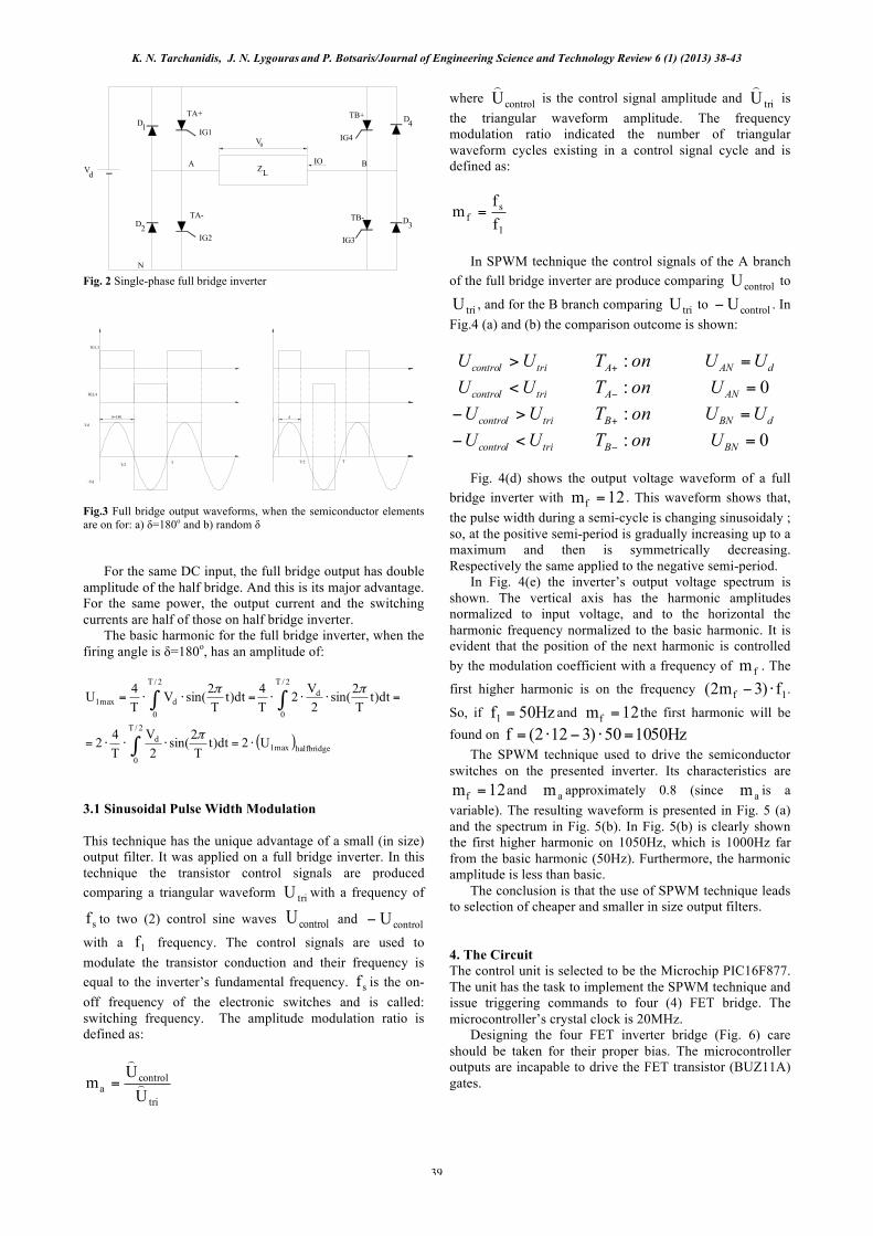
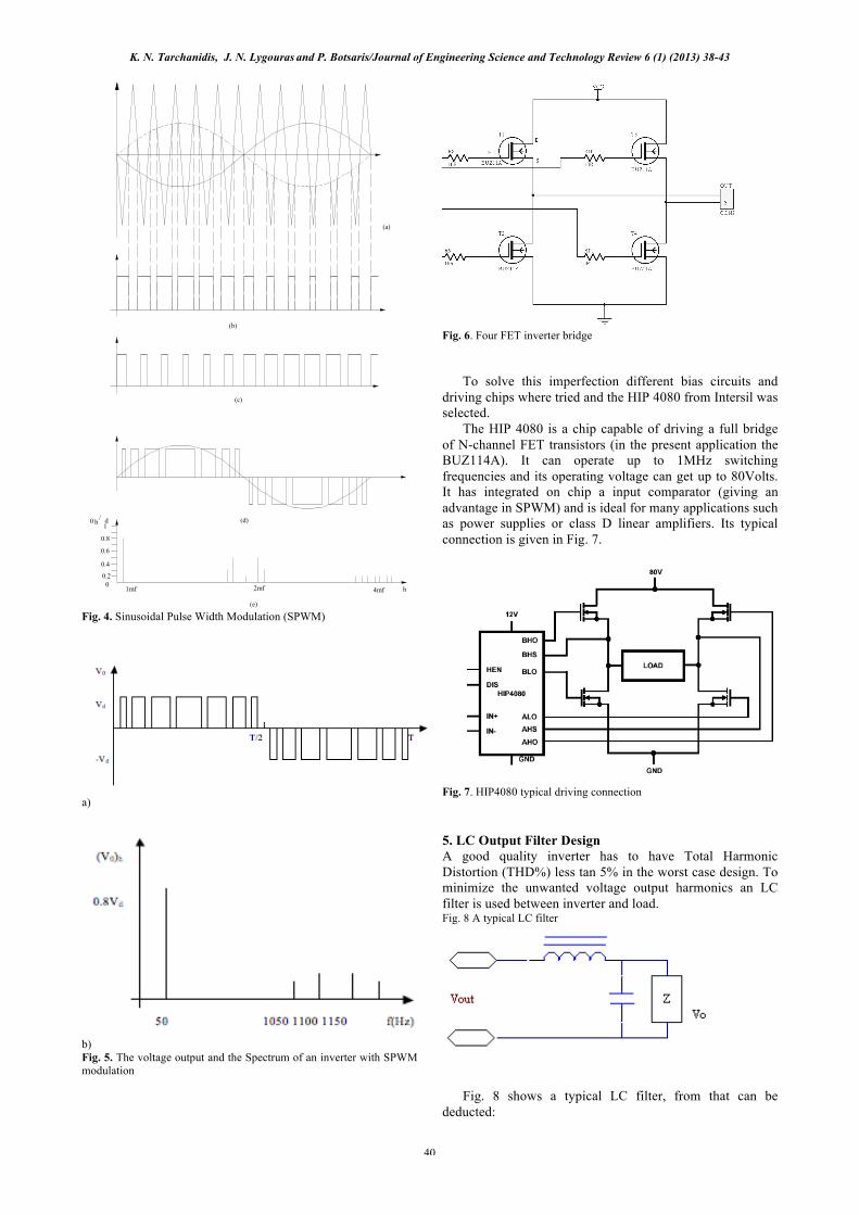
3. Single phase full bridge inverter Full bridge inverter circuit diagram is shown in Fig.2 and Fig.3. It is clear that the full bridge is consisted by two half bridges. On Fig.3 are shown the full bridge output waveforms for different firing angles.
Jestr JOURNAL OF Engineering Science and Technology Review
www.jestr.org
______________ * E-mail address: [email protected] ISSN: 1791-2377 © 2013 Kavala Institute of Technology. All rights reserved.
K. N. Tarchanidis, J. N. Lygouras and P. Botsaris/Journal of Engineering Science and Technology Review 6 (1) (2013) 38-43
39
V0
ZLVd
D1
D2
N
TA+
TA-
A
IG1
IG2
IG4
IG3
TB+
TB-
B
D4
D3
IO
Fig. 2 Single-phase full bridge inverter
δ=180 δ
IG1,3
IG2,4
Vd
-Vd
T/2 T T/2 T
Fig.3 Full bridge output waveforms, when the semiconductor elements are on for: a) δ=180ο and b) random δ For the same DC input, the full bridge output has double amplitude of the half bridge. And this is its major advantage. For the same power, the output current and the switching currents are half of those on half bridge inverter. The basic harmonic for the full bridge inverter, when the firing angle is δ=180ο, has an amplitude of:
( )∫
∫∫
⋅=⋅⋅⋅=
=⋅⋅⋅=⋅⋅=
2/T
0halfbridgemax1
d
2/T
0
d2/T
0dmax1
U2dt)tT2sin(
2V
T42
dt)tT2sin(
2V2
T4dt)t
T2sin(V
T4U
π
ππ
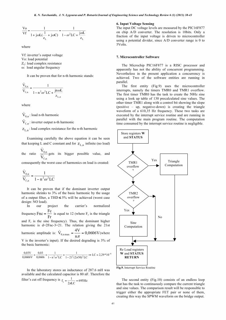
3.1 Sinusoidal Pulse Width Modulation This technique has the unique advantage of a small (in size) output filter. It was applied on a full bridge inverter. In this technique the transistor control signals are produced comparing a triangular waveform triU with a frequency of
sf to two (2) control sine waves controlU and controlU−
with a 1f frequency. The control signals are used to modulate the transistor conduction and their frequency is equal to the inverter’s fundamental frequency. sf is the on-off frequency of the electronic switches and is called: switching frequency. The amplitude modulation ratio is defined as:
tri
controla U
Um
=
where controlU
is the control signal amplitude and triU
is the triangular waveform amplitude. The frequency modulation ratio indicated the number of triangular waveform cycles existing in a control signal cycle and is defined as:
1
sf f
fm =
In SPWM technique the control signals of the A branch of the full bridge inverter are produce comparing controlU to
triU , and for the B branch comparing triU to controlU− . In Fig.4 (a) and (b) the comparison outcome is shown:
tricontrol UU > onTA :+ dAN UU =
tricontrol UU < onTA :− 0=ANU
tricontrol UU >− onTB :+ dBN UU =
tricontrol UU <− onTB :− 0=BNU Fig. 4(d) shows the output voltage waveform of a full bridge inverter with 12mf = . This waveform shows that, the pulse width during a semi-cycle is changing sinusoidaly ; so, at the positive semi-period is gradually increasing up to a maximum and then is symmetrically decreasing. Respectively the same applied to the negative semi-period. In Fig. 4(e) the inverter’s output voltage spectrum is shown. The vertical axis has the harmonic amplitudes normalized to input voltage, and to the horizontal the harmonic frequency normalized to the basic harmonic. It is evident that the position of the next harmonic is controlled by the modulation coefficient with a frequency of fm . The
first higher harmonic is on the frequency 1f f)3m2( ⋅− .
So, if Hz50f1 = and 12mf = the first harmonic will be found on Hz105050)3122(f =⋅−⋅= The SPWM technique used to drive the semiconductor switches on the presented inverter. Its characteristics are
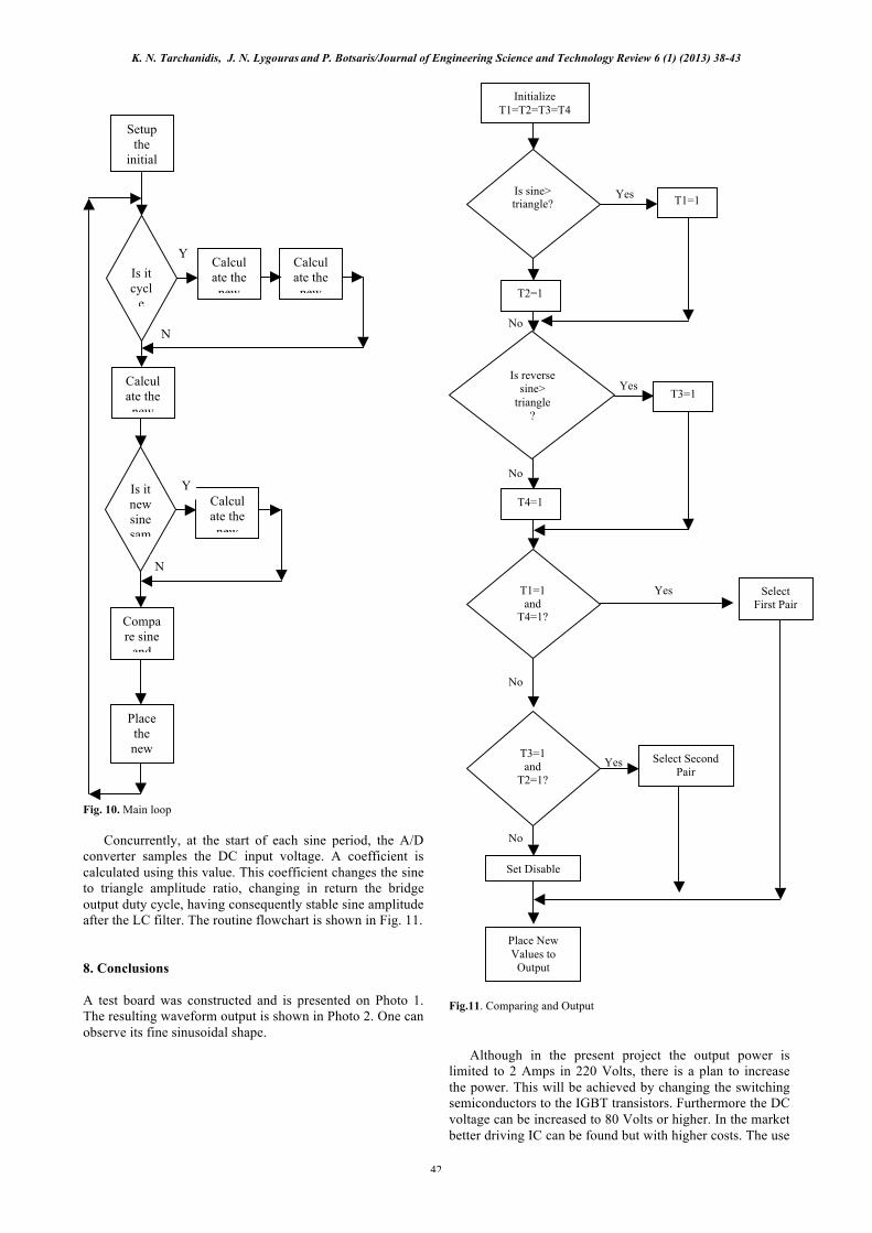
12mf = and am approximately 0.8 (since am is a variable). The resulting waveform is presented in Fig. 5 (a) and the spectrum in Fig. 5(b). In Fig. 5(b) is clearly shown the first higher harmonic on 1050Hz, which is 1000Hz far from the basic harmonic (50Hz). Furthermore, the harmonic amplitude is less than basic. The conclusion is that the use of SPWM technique leads to selection of cheaper and smaller in size output filters. 4. The Circuit The control unit is selected to be the Microchip PIC16F877. The unit has the task to implement the SPWM technique and issue triggering commands to four (4) FET bridge. The microcontroller’s crystal clock is 20MHz. Designing the four FET inverter bridge (Fig. 6) care should be taken for their proper bias. The microcontroller outputs are incapable to drive the FET transistor (BUZ11A) gates.
K. N. Tarchanidis, J. N. Lygouras and P. Botsaris/Journal of Engineering Science and Technology Review 6 (1) (2013) 38-43
40
(a)
(b)
(c)
(d)
(e)
1
00.2
1mf 2mf 4mf
0 h / d
0.8
0.4
0.6
h
Fig. 4. Sinusoidal Pulse Width Modulation (SPWM)
a)
b) Fig. 5. The voltage output and the Spectrum of an inverter with SPWM modulation
Fig. 6. Four FET inverter bridge To solve this imperfection different bias circuits and driving chips where tried and the HIP 4080 from Intersil was selected. The HIP 4080 is a chip capable of driving a full bridge of N-channel FET transistors (in the present application the BUZ114A). It can operate up to 1MHz switching frequencies and its operating voltage can get up to 80Volts. It has integrated on chip a input comparator (giving an advantage in SPWM) and is ideal for many applications such as power supplies or class D linear amplifiers. Its typical connection is given in Fig. 7.
Fig. 7. HIP4080 typical driving connection 5. LC Output Filter Design A good quality inverter has to have Total Harmonic Distortion (THD%) less tan 5% in the worst case design. To minimize the unwanted voltage output harmonics an LC filter is used between inverter and load. Fig. 8 A typical LC filter
Fig. 8 shows a typical LC filter, from that can be deducted:
K. N. Tarchanidis, J. N. Lygouras and P. Botsaris/Journal of Engineering Science and Technology Review 6 (1) (2013) 38-43
41
L
2
L zLjLC1
1
)Cjz1(Lj1
1VfVo
ωωωω +−
=++
=
where Vf: inverter’s output voltage Vo: load potential ΖL: load complex resistance ω: load angular frequency It can be proven that for n-th harmonic stands:
n,L
22n,f
n,0
zLjnLCn1
1VV
ωω +−
=
where
n,0V
: load n-th harmonic
n,fV
: inverter output n-th harmonic
n,Lz : load complex resistance for the n-th harmonic Examining carefully the above equation it can be seen that keeping L and C constant and for n,Lz infinite (no load)
the ratio n,f
n,0
VV
gets its bigger possible value, and
consequently the worst case of harmonics on load is created:
LCn11
VV
22n,f
n,0
ω−=
It can be proven that if the dominant inverter output harmonic shrinks to 3% of the basic harmonic by the usage of a output filter, a THD≤ 5% will be achieved (worst case design: NO load). In our project the carrier’s normalized
frequencyFrFcFnc = is equal to 12 (where Fc is the triangle
and Fr is the sine frequency). Thus, the dominant higher harmonic is d=2Fnc-3=21. The relation giving the 21st
harmonic amplitude is: V0606,0nV4V maxn,0 ==π
(where
V is the inverter’s input). If the desired degrading is 3% of the basic harmonic:
82222 10*29,2LCLC)502(211
1LCn1
10606,003,0
V0606,0V03,0 −=⇒
−=
−==
πω In the laboratory stores an inductance of 287.6 mH was available and the calculated capacitor is 80 nF. Therefore the filter’s cut off frequency is Hz695
LC21fc ==π
6. Input Voltage Sensing The input DC voltage levels are measured by the PIC16F877 on chip A/D converter. The resolution is 10bits. Only a fraction of the input voltage is driven to microcontroller using a potential divider, since A/D converter range is 0 to 5Volts. 7. Microcontroller Software The Microchip PIC16F877 is a RISC processor and apparently has not the ability of concurrent programming. Nevertheless in the present application a concurrency is achieved. Two of the software entities are running in parallel. The first entity (Fig.9) uses the microcontroller interrupts, namely the timers TMR0 and TMR1 overflow. The first timer TMR0 has the task to create the 50Hz sine using a look up table of 130 precalculated sine values. The other timer TMR1 along with a control bit showing the slope (positive – up, negative-down) is creating the triangle waveform of a 610,35 Hz frequency. These two tasks are executed by the interrupt service routine and are running in parallel with the main program routine. The computation time consumed by the interrupt service routine is negligible.
Fig.9. Interrupt Service Routine
The second entity (Fig.10) consists of an endless loop that has the task to continuously compare the current triangle and sine values. The comparison result will be responsible to trigger either the appropriate FET pair or none of them, creating this way the SPWM waveform on the bridge output.
Store registers W and STATUS
TMR1 overflow
?
Triangle
Computation
TMR2 overflow
?
Sine
Computation
Re Load registers W and STATUS
RETURN
Yes
No
Yes
K. N. Tarchanidis, J. N. Lygouras and P. Botsaris/Journal of Engineering Science and Technology Review 6 (1) (2013) 38-43
42
Fig. 10. Main loop
Concurrently, at the start of each sine period, the A/D converter samples the DC input voltage. A coefficient is calculated using this value. This coefficient changes the sine to triangle amplitude ratio, changing in return the bridge output duty cycle, having consequently stable sine amplitude after the LC filter. The routine flowchart is shown in Fig. 11.
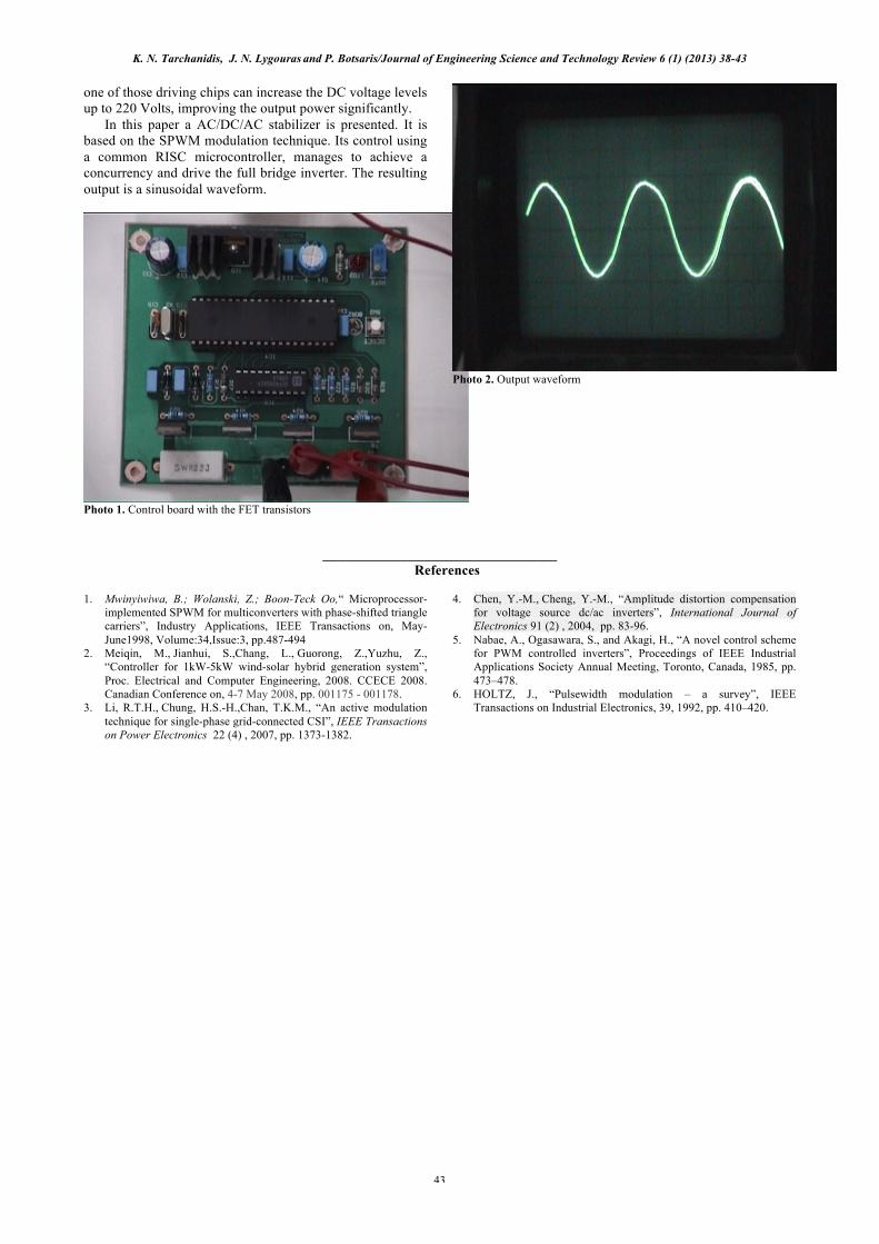
8. Conclusions A test board was constructed and is presented on Photo 1. The resulting waveform output is shown in Photo 2. One can observe its fine sinusoidal shape.
Fig.11. Comparing and Output Although in the present project the output power is limited to 2 Amps in 220 Volts, there is a plan to increase the power. This will be achieved by changing the switching semiconductors to the IGBT transistors. Furthermore the DC voltage can be increased to 80 Volts or higher. In the market better driving IC can be found but with higher costs. The use
Setup the
initial values
Is it cycl
e start
?
YES
Calculate the new sine
coefficient
Calculate the new sine shift
Calculate the new
triangle
Is it new sine sample?
Calculate the new sine
Compare sine
and triangl
e values Place the new
values to
output pins
YES
NO
Yes
NO
Initialize T1=T2=T3=T4
Is sine> triangle? T1=1
T2=1
Is reverse sine>
triangle ?
T3=1
T4=1
T1=1 and
T4=1?
Select First Pair
T3=1 and
T2=1?
Select Second Pair
Set Disable
Place New Values to
Output
Yes
Yes
Yes
Yes
No
No
No
No
K. N. Tarchanidis, J. N. Lygouras and P. Botsaris/Journal of Engineering Science and Technology Review 6 (1) (2013) 38-43
43
one of those driving chips can increase the DC voltage levels up to 220 Volts, improving the output power significantly. In this paper a AC/DC/AC stabilizer is presented. It is based on the SPWM modulation technique. Its control using a common RISC microcontroller, manages to achieve a concurrency and drive the full bridge inverter. The resulting output is a sinusoidal waveform.
Photo 1. Control board with the FET transistors
Photo 2. Output waveform
______________________________
References 1. Mwinyiwiwa, B.; Wolanski, Z.; Boon-Teck Oo,“ Microprocessor-
implemented SPWM for multiconverters with phase-shifted triangle carriers”, Industry Applications, IEEE Transactions on, May-June1998, Volume:34,Issue:3, pp.487-494
2. Meiqin, M., Jianhui, S.,Chang, L., Guorong, Z.,Yuzhu, Z., “Controller for 1kW-5kW wind-solar hybrid generation system”, Proc. Electrical and Computer Engineering, 2008. CCECE 2008. Canadian Conference on, 4-7 May 2008, pp. 001175 - 001178.
3. Li, R.T.H., Chung, H.S.-H.,Chan, T.K.M., “An active modulation technique for single-phase grid-connected CSI”, IEEE Transactions on Power Electronics 22 (4) , 2007, pp. 1373-1382.
4. Chen, Y.-M., Cheng, Y.-M., “Amplitude distortion compensation for voltage source dc/ac inverters”, International Journal of Electronics 91 (2) , 2004, pp. 83-96.
5. Nabae, A., Ogasawara, S., and Akagi, H., “A novel control scheme for PWM controlled inverters”, Proceedings of IEEE Industrial Applications Society Annual Meeting, Toronto, Canada, 1985, pp. 473–478.
6. HOLTZ, J., “Pulsewidth modulation – a survey”, IEEE Transactions on Industrial Electronics, 39, 1992, pp. 410–420.