Embed Size (px)
Citation preview
Distance and Speed Measurements using FPGA andASIC on a high data rate system
Abdul Rehman Buzdar, Liguo Sun, Azhar Latif, Abdullah BuzdarDepartment of Electronic Engineering and Information Science
University of Science and Technology of China (USTC)Hefei, Peoples Republic of China
Abstract—This paper deals with the implementation of FPGAand ASIC designs to calculate the distance and speed of a movingremote object using laser source and echo pulses reflected fromthat remote object. The project proceeded in three phases for theFPGA implementation: All-in-C design using Xilinx Microblazesoft core processor system, an accelerated design with customco-processor and Microblaze soft core processor system, and fullcustom hardware design implemented using VHDL on XilinxFPGA. Later the complete system was implemented on ASIC.The ASIC implementation optimized the modules for area andtiming for a 130nm process technology.
Keywords—Distance; Speed; FPGA; MicroBaze; Co-Design;ASIC
I. INTRODUCTION
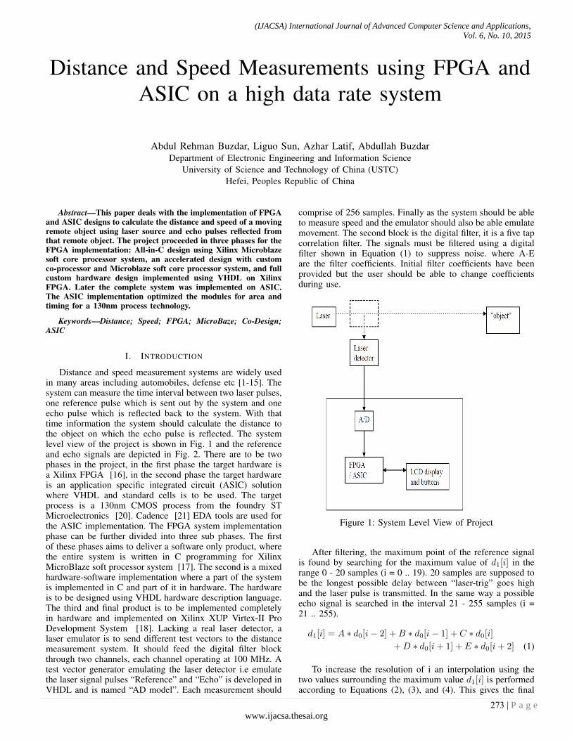
Distance and speed measurement systems are widely usedin many areas including automobiles, defense etc [1-15]. Thesystem can measure the time interval between two laser pulses,one reference pulse which is sent out by the system and oneecho pulse which is reflected back to the system. With thattime information the system should calculate the distance tothe object on which the echo pulse is reflected. The systemlevel view of the project is shown in Fig. 1 and the referenceand echo signals are depicted in Fig. 2. There are to be twophases in the project, in the first phase the target hardware isa Xilinx FPGA [16], in the second phase the target hardwareis an application specific integrated circuit (ASIC) solutionwhere VHDL and standard cells is to be used. The targetprocess is a 130nm CMOS process from the foundry STMicroelectronics [20]. Cadence [21] EDA tools are used forthe ASIC implementation. The FPGA system implementationphase can be further divided into three sub phases. The firstof these phases aims to deliver a software only product, wherethe entire system is written in C programming for XilinxMicroBlaze soft processor system [17]. The second is a mixedhardware-software implementation where a part of the systemis implemented in C and part of it in hardware. The hardwareis to be designed using VHDL hardware description language.The third and final product is to be implemented completelyin hardware and implemented on Xilinx XUP Virtex-II ProDevelopment System [18]. Lacking a real laser detector, alaser emulator is to send different test vectors to the distancemeasurement system. It should feed the digital filter blockthrough two channels, each channel operating at 100 MHz. Atest vector generator emulating the laser detector i.e emulatethe laser signal pulses “Reference” and “Echo” is developed inVHDL and is named “AD model”. Each measurement should
comprise of 256 samples. Finally as the system should be ableto measure speed and the emulator should also be able emulatemovement. The second block is the digital filter, it is a five tapcorrelation filter. The signals must be filtered using a digitalfilter shown in Equation (1) to suppress noise. where A-Eare the filter coefficients. Initial filter coefficients have beenprovided but the user should be able to change coefficientsduring use.
Figure 1: System Level View of Project
After filtering, the maximum point of the reference signalis found by searching for the maximum value of d1[i] in therange 0 - 20 samples (i = 0 .. 19). 20 samples are supposed tobe the longest possible delay between “laser-trig” goes highand the laser pulse is transmitted. In the same way a possibleecho signal is searched in the interval 21 - 255 samples (i =21 .. 255).
d1[i] = A ∗ d0[i− 2] +B ∗ d0[i− 1] + C ∗ d0[i]+D ∗ d0[i+ 1] + E ∗ d0[i+ 2] (1)
To increase the resolution of i an interpolation using thetwo values surrounding the maximum value d1[i] is performedaccording to Equations (2), (3), and (4). This gives the final
(IJACSA) International Journal of Advanced Computer Science and Applications,
Vol. 6, No. 10, 2015
273 | P a g ewww.ijacsa.thesai.org
time sample point j.
b = d1[i− 1]− d1[i+ 1] (2)
c = 2 ∗ (d1[i− 1]− 2 ∗ d1[i] + d1[i+ 1]) (3)
j = i+ b/c (4)
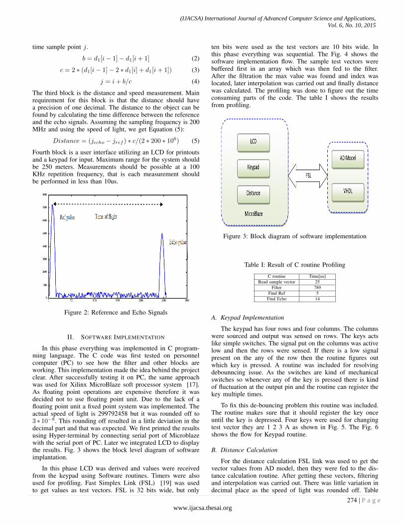
The third block is the distance and speed measurement. Mainrequirement for this block is that the distance should havea precision of one decimal. The distance to the object can befound by calculating the time difference between the referenceand the echo signals. Assuming the sampling frequency is 200MHz and using the speed of light, we get Equation (5):
Distance = (jecho − jref ) ∗ c/(2 ∗ 200 ∗ 106) (5)
Fourth block is a user interface utilizing an LCD for printoutsand a keypad for input. Maximum range for the system shouldbe 250 meters. Measurements should be possible at a 100KHz repetition frequency, that is each measurement shouldbe performed in less than 10us.
Figure 2: Reference and Echo Signals
II. SOFTWARE IMPLEMENTATION
In this phase everything was implemented in C program-ming language. The C code was first tested on personnelcomputer (PC) to see how the filter and other blocks areworking. This implementation made the idea behind the projectclear. After successfully testing it on PC, the same approachwas used for Xilinx MicroBlaze soft processor system [17].As floating point operations are expensive therefore it wasdecided not to use floating point unit. Due to the lack of afloating point unit a fixed point system was implemented. Theactual speed of light is 299792458 but it was rounded off to3 ∗ 10−8. This rounding off resulted in a little deviation in thedecimal part and that was expected. We first printed the resultsusing Hyper-terminal by connecting serial port of Microblazewith the serial port of PC. Later we integrated LCD to displaythe results. Fig. 3 shows the block level diagram of softwareimplantation.
In this phase LCD was derived and values were receivedfrom the keypad using Software routines. Timers were alsoused for profiling. Fast Simplex Link (FSL) [19] was usedto get values as test vectors. FSL is 32 bits wide, but only
ten bits were used as the test vectors are 10 bits wide. Inthis phase everything was sequential. The Fig. 4 shows thesoftware implementation flow. The sample test vectors werebuffered first in an array which was then fed to the filter.After the filtration the max value was found and index waslocated, later interpolation was carried out and finally distancewas calculated. The profiling was done to figure out the timeconsuming parts of the code. The table I shows the resultsfrom profiling.
Figure 3: Block diagram of software implementation
Table I: Result of C routine Profiling
C routine Time[us]Read sample vector 25
Filter 789Find Ref 5
Find Echo 14
A. Keypad Implementation
The keypad has four rows and four columns. The columnswere sourced and output was sensed on rows. The keys actslike simple switches. The signal put on the columns was activelow and then the rows were sensed. If there is a low signalpresent on the any of the row then the routine figures outwhich key is pressed. A routine was included for resolvingdebounncing issue. As the switches are kind of mechanicalswitches so whenever any of the key is pressed there is kindof fluctuation at the output pin and the routine can register thekey multiple times.
To fix this de-bouncing problem this routine was included.The routine makes sure that it should register the key onceuntil the key is depressed. Four keys were used for changingtest vector they are 1 2 3 A as shown in Fig. 5. The Fig. 6shows the flow for Keypad routine.
B. Distance Calculation
For the distance calculation FSL link was used to get thevector values from AD model, then they were fed to the dis-tance calculation routine. After getting these vectors, filteringand interpolation was carried out. There was little variation indecimal place as the speed of light was rounded off. Table
(IJACSA) International Journal of Advanced Computer Science and Applications,
Vol. 6, No. 10, 2015
274 | P a g ewww.ijacsa.thesai.org
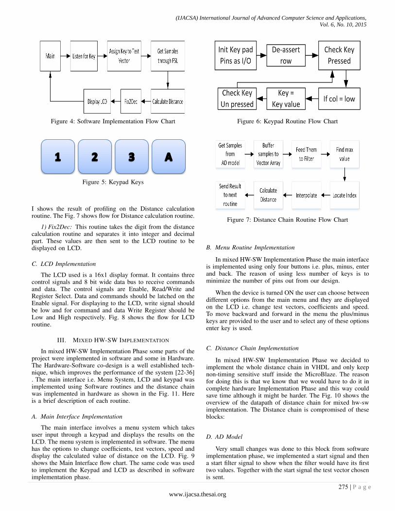
Figure 4: Software Implementation Flow Chart
Figure 5: Keypad Keys
I shows the result of profiling on the Distance calculationroutine. The Fig. 7 shows flow for Distance calculation routine.
1) Fix2Dec: This routine takes the digit from the distancecalculation routine and separates it into integer and decimalpart. These values are then sent to the LCD routine to bedisplayed on LCD.
C. LCD Implementation
The LCD used is a 16x1 display format. It contains threecontrol signals and 8 bit wide data bus to receive commandsand data. The control signals are Enable, Read/Write andRegister Select. Data and commands should be latched on theEnable signal. For displaying to the LCD, write signal shouldbe low and for command and data Write Register should beLow and High respectively. Fig. 8 shows the flow for LCDroutine.
III. MIXED HW-SW IMPLEMENTATION
In mixed HW-SW Implementation Phase some parts of theproject were implemented in software and some in Hardware.The Hardware-Software co-design is a well established tech-nique, which improves the performance of the system [22-36]. The main interface i.e. Menu System, LCD and keypad wasimplemented using Software routines and the distance chainwas implemented in hardware as shown in the Fig. 11. Hereis a brief description of each routine.
A. Main Interface Implementation
The main interface involves a menu system which takesuser input through a keypad and displays the results on theLCD. The menu system is implemented in software. The menuhas the options to change coefficients, test vectors, speed anddisplay the calculated value of distance on the LCD. Fig. 9shows the Main Interface flow chart. The same code was usedto implement the Keypad and LCD as described in softwareimplementation phase.
Figure 6: Keypad Routine Flow Chart
Figure 7: Distance Chain Routine Flow Chart
B. Menu Routine Implementation
In mixed HW-SW Implementation Phase the main interfaceis implemented using only four buttons i.e. plus, minus, enterand back. The reason of using less number of keys is tominimize the number of pins out from our design.
When the device is turned ON the user can choose betweendifferent options from the main menu and they are displayedon the LCD i.e. change test vectors, coefficients and speed.To move backward and forward in the menu the plus/minuskeys are provided to the user and to select any of these optionsenter key is used.
C. Distance Chain Implementation
In mixed HW-SW Implementation Phase we decided toimplement the whole distance chain in VHDL and only keepnon-timing sensitive stuff inside the MicroBlaze. The reasonfor doing this is that we know that we would have to do it incomplete hardware Implementation Phase and this way couldsave time although it might be harder. The Fig. 10 shows theoverview of the datapath of distance chain for mixed hw-swimplementation. The Distance chain is compromised of theseblocks:
D. AD Model
Very small changes was done to this block from softwareimplementation phase, we implemented a start signal and thena start filter signal to show when the filter would have its firsttwo values. Together with the start signal the test vector chosenis sent.
(IJACSA) International Journal of Advanced Computer Science and Applications,
Vol. 6, No. 10, 2015
275 | P a g ewww.ijacsa.thesai.org
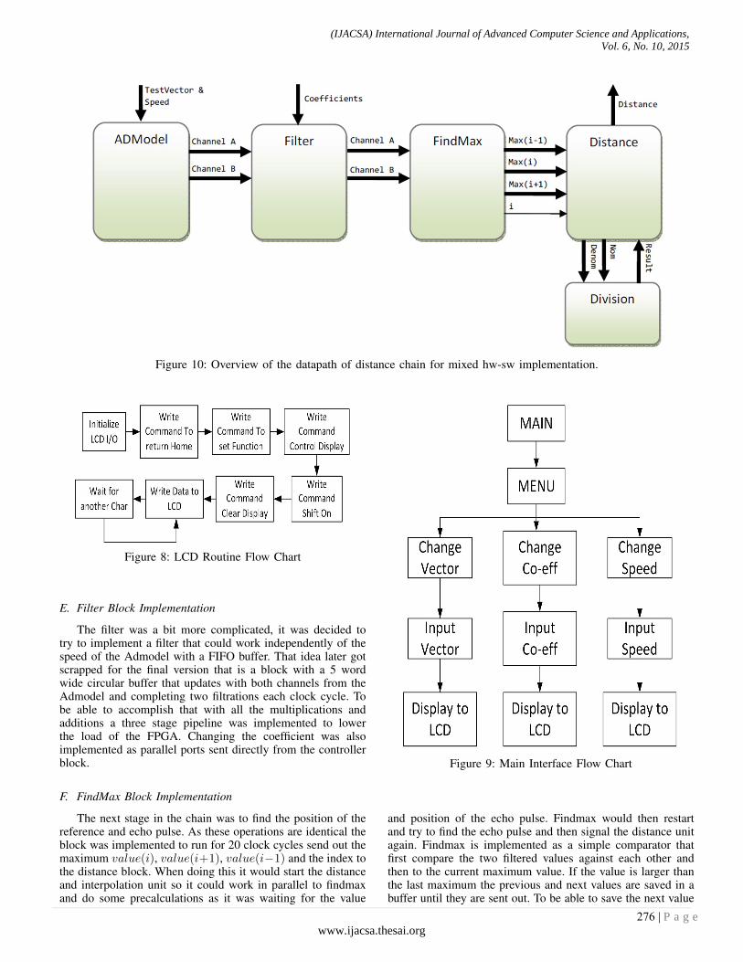
Figure 10: Overview of the datapath of distance chain for mixed hw-sw implementation.
Figure 8: LCD Routine Flow Chart
E. Filter Block Implementation
The filter was a bit more complicated, it was decided totry to implement a filter that could work independently of thespeed of the Admodel with a FIFO buffer. That idea later gotscrapped for the final version that is a block with a 5 wordwide circular buffer that updates with both channels from theAdmodel and completing two filtrations each clock cycle. Tobe able to accomplish that with all the multiplications andadditions a three stage pipeline was implemented to lowerthe load of the FPGA. Changing the coefficient was alsoimplemented as parallel ports sent directly from the controllerblock.
F. FindMax Block Implementation
The next stage in the chain was to find the position of thereference and echo pulse. As these operations are identical theblock was implemented to run for 20 clock cycles send out themaximum value(i), value(i+1), value(i−1) and the index tothe distance block. When doing this it would start the distanceand interpolation unit so it could work in parallel to findmaxand do some precalculations as it was waiting for the value
Figure 9: Main Interface Flow Chart
and position of the echo pulse. Findmax would then restartand try to find the echo pulse and then signal the distance unitagain. Findmax is implemented as a simple comparator thatfirst compare the two filtered values against each other andthen to the current maximum value. If the value is larger thanthe last maximum the previous and next values are saved in abuffer until they are sent out. To be able to save the next value
(IJACSA) International Journal of Advanced Computer Science and Applications,
Vol. 6, No. 10, 2015
276 | P a g ewww.ijacsa.thesai.org
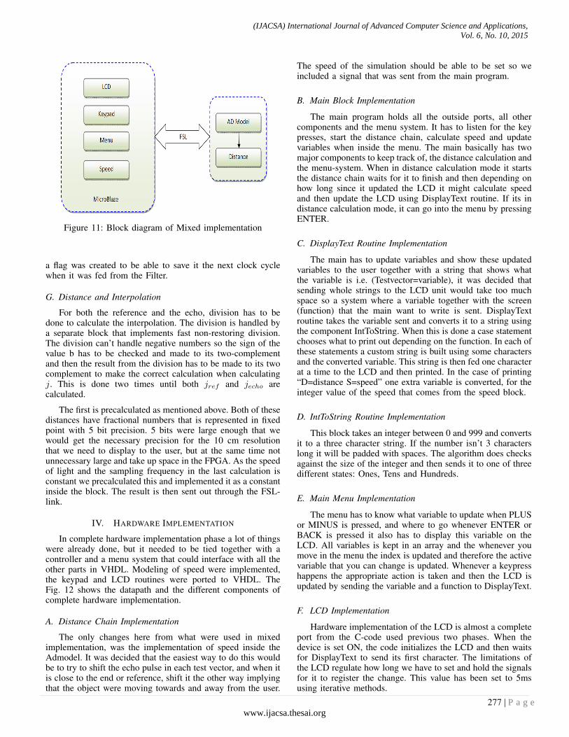
Figure 11: Block diagram of Mixed implementation
a flag was created to be able to save it the next clock cyclewhen it was fed from the Filter.
G. Distance and Interpolation
For both the reference and the echo, division has to bedone to calculate the interpolation. The division is handled bya separate block that implements fast non-restoring division.The division can’t handle negative numbers so the sign of thevalue b has to be checked and made to its two-complementand then the result from the division has to be made to its twocomplement to make the correct calculation when calculatingj. This is done two times until both jref and jecho arecalculated.
The first is precalculated as mentioned above. Both of thesedistances have fractional numbers that is represented in fixedpoint with 5 bit precision. 5 bits were large enough that wewould get the necessary precision for the 10 cm resolutionthat we need to display to the user, but at the same time notunnecessary large and take up space in the FPGA. As the speedof light and the sampling frequency in the last calculation isconstant we precalculated this and implemented it as a constantinside the block. The result is then sent out through the FSL-link.
IV. HARDWARE IMPLEMENTATION
In complete hardware implementation phase a lot of thingswere already done, but it needed to be tied together with acontroller and a menu system that could interface with all theother parts in VHDL. Modeling of speed were implemented,the keypad and LCD routines were ported to VHDL. TheFig. 12 shows the datapath and the different components ofcomplete hardware implementation.
A. Distance Chain Implementation
The only changes here from what were used in mixedimplementation, was the implementation of speed inside theAdmodel. It was decided that the easiest way to do this wouldbe to try to shift the echo pulse in each test vector, and when itis close to the end or reference, shift it the other way implyingthat the object were moving towards and away from the user.
The speed of the simulation should be able to be set so weincluded a signal that was sent from the main program.
B. Main Block Implementation
The main program holds all the outside ports, all othercomponents and the menu system. It has to listen for the keypresses, start the distance chain, calculate speed and updatevariables when inside the menu. The main basically has twomajor components to keep track of, the distance calculation andthe menu-system. When in distance calculation mode it startsthe distance chain waits for it to finish and then depending onhow long since it updated the LCD it might calculate speedand then update the LCD using DisplayText routine. If its indistance calculation mode, it can go into the menu by pressingENTER.
C. DisplayText Routine Implementation
The main has to update variables and show these updatedvariables to the user together with a string that shows whatthe variable is i.e. (Testvector=variable), it was decided thatsending whole strings to the LCD unit would take too muchspace so a system where a variable together with the screen(function) that the main want to write is sent. DisplayTextroutine takes the variable sent and converts it to a string usingthe component IntToString. When this is done a case statementchooses what to print out depending on the function. In each ofthese statements a custom string is built using some charactersand the converted variable. This string is then fed one characterat a time to the LCD and then printed. In the case of printing“D=distance S=speed” one extra variable is converted, for theinteger value of the speed that comes from the speed block.
D. IntToString Routine Implementation
This block takes an integer between 0 and 999 and convertsit to a three character string. If the number isn’t 3 characterslong it will be padded with spaces. The algorithm does checksagainst the size of the integer and then sends it to one of threedifferent states: Ones, Tens and Hundreds.
E. Main Menu Implementation
The menu has to know what variable to update when PLUSor MINUS is pressed, and where to go whenever ENTER orBACK is pressed it also has to display this variable on theLCD. All variables is kept in an array and the whenever youmove in the menu the index is updated and therefore the activevariable that you can change is updated. Whenever a keypresshappens the appropriate action is taken and then the LCD isupdated by sending the variable and a function to DisplayText.
F. LCD Implementation
Hardware implementation of the LCD is almost a completeport from the C-code used previous two phases. When thedevice is set ON, the code initializes the LCD and then waitsfor DisplayText to send its first character. The limitations ofthe LCD regulate how long we have to set and hold the signalsfor it to register the change. This value has been set to 5msusing iterative methods.
(IJACSA) International Journal of Advanced Computer Science and Applications,
Vol. 6, No. 10, 2015
277 | P a g ewww.ijacsa.thesai.org
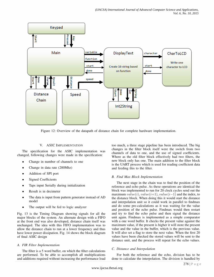
Figure 12: Overview of the datapath of distance chain for complete hardware implementation.
V. ASIC IMPLEMENTATION
The specification for the ASIC implementation waschanged, following changes were made in the specification:
• Change in number of channels to one
• Change in data rate (200Mhz)
• Addition of SPI port
• Signed Coefficients
• Taps input Serially during initialization
• Result is in decimeter
• The data is input from pattern generator instead of ADmodel
• The output will be fed to logic analyzer
Fig. 13 is the Timing Diagram showing signals for all themajor blocks of the system. An alternate design with a FIFOat the front end was also developed, distance chain itself wasunchanged. The idea with this FIFO implementation was toallow the distance chain to run at a lower frequency and thushave lower power dissipation. Fig. 14 shows the block diagramof final ASIC design
A. FIR Filter Implementation
The filter is a 5 word buffer, on which the filter calculationsare performed. To be able to accomplish all multiplicationsand additions required without increasing the performance load
too much, a three stage pipeline has been introduced. The bigchanges in the filter block itself were the switch from twochannels of data to one, and the use of signed coefficients.Where as the old filter block effectively had two filters, thenew block only has one. The main addition to the filter blockis the UART process which is used for reading coefficient dataand feeding this to the filter.
B. Find Max Block Implementation
The next stage in the chain was to find the position of thereference and echo pulse. As these operations are identical theblock was implemented to run for 20 clock cycles send out themaximum value(i), value(i+1), value(i−1) and the index, tothe distance block. When doing this it would start the distanceand interpolation unit so it could work in parallel to findmaxand do some pre-calculations as it was waiting for the valueand position of the echo pulse. Findmax would then restartand try to find the echo pulse and then signal the distanceunit again. Findmax is implemented as a simple comparatorwith a one word buffer. It checks the present value against themaximum value, if the present is higher it will store the presentvalue and the value in the buffer, which is the previous value.It will also set a flag to store the next value. When the first 20values have been checked the stored values will be sent to thedistance unit, and the process will repeat for the echo values.
C. Distance and Interpolation
For both the reference and the echo, division has to bedone to calculate the interpolation. The division is handled by
(IJACSA) International Journal of Advanced Computer Science and Applications,
Vol. 6, No. 10, 2015
278 | P a g ewww.ijacsa.thesai.org
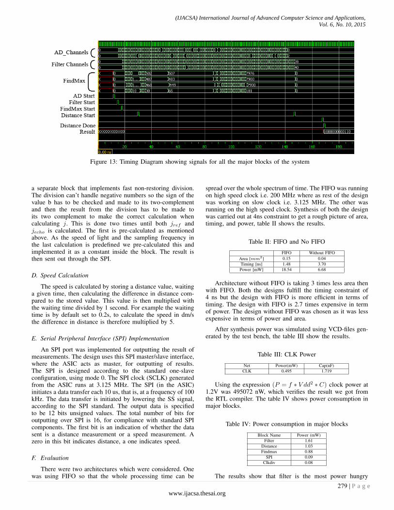
Figure 13: Timing Diagram showing signals for all the major blocks of the system
a separate block that implements fast non-restoring division.The division can’t handle negative numbers so the sign of thevalue b has to be checked and made to its two-complementand then the result from the division has to be made toits two complement to make the correct calculation whencalculating j. This is done two times until both jref andjecho is calculated. The first is pre-calculated as mentionedabove. As the speed of light and the sampling frequency inthe last calculation is predefined we pre-calculated this andimplemented it as a constant inside the block. The result isthen sent out through the SPI.
D. Speed Calculation
The speed is calculated by storing a distance value, waitinga given time, then calculating the difference in distance com-pared to the stored value. This value is then multiplied withthe waiting time divided by 1 second. For example the waitingtime is by default set to 0.2s, to calculate the speed in dm/sthe difference in distance is therefore multiplied by 5.
E. Serial Peripheral Interface (SPI) Implementation
An SPI port was implemented for outputting the result ofmeasurements. The design uses this SPI master/slave interface,where the ASIC acts as master, for outputting of results.The SPI is designed according to the standard one-slaveconfiguration, using mode 0. The SPI clock (SCLK) generatedfrom the ASIC runs at 3.125 MHz. The SPI (in the ASIC)initiates a data transfer each 10 us, that is, at a frequency of 100kHz. The data transfer is initiated by lowering the SS signal,according to the SPI standard. The output data is specifiedto be 12 bits unsigned values. The total number of bits foroutputting over SPI is 16, for compliance with standard SPIcomponents. The first bit is an indication of whether the datasent is a distance measurement or a speed measurement. Azero in this bit indicates distance, a one indicates speed.
F. Evaluation
There were two architectures which were considered. Onewas using FIFO so that the whole processing time can be
spread over the whole spectrum of time. The FIFO was runningon high speed clock i.e. 200 MHz where as rest of the designwas working on slow clock i.e. 3.125 MHz. The other wasrunning on the high speed clock. Synthesis of both the designwas carried out at 4ns constraint to get a rough picture of area,timing, and power, table II shows the results.
Table II: FIFO and No FIFO
FIFO Without FIFOArea [mm2] 0.15 0.04Timing [ns] 1.48 3.70Power [mW] 18.54 6.68
Architecture without FIFO is taking 3 times less area thenwith FIFO. Both the designs fulfill the timing constraint of4 ns but the design with FIFO is more efficient in terms oftiming. The design with FIFO is 2.7 times expensive in termof power. The design without FIFO was chosen as it was lessexpensive in terms of power and area.
After synthesis power was simulated using VCD-files gen-erated by the test bench, the table III show the results.
Table III: CLK Power
Net Power(mW) Cap(nF)CLK 0.495 1.719
Using the expression (P = f ∗ V dd2 ∗ C) clock power at1.2V was 495072 nW, which verifies the result we got fromthe RTL compiler. The table IV shows power consumption inmajor blocks.
Table IV: Power consumption in major blocks
Block Name Power (mW)Filter 1.61
Distance 1.03Findmax 0.88
SPI 0.09Clkdiv 0.08
The results show that filter is the most power hungry
(IJACSA) International Journal of Advanced Computer Science and Applications,
Vol. 6, No. 10, 2015
279 | P a g ewww.ijacsa.thesai.org
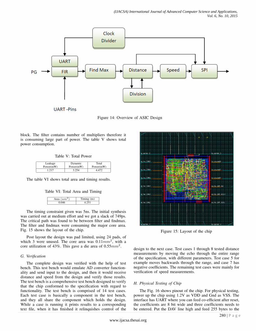
Figure 14: Overview of ASIC Design
block. The filter contains number of multipliers therefore itis consuming large part of power. The table V shows totalpower consumption.
Table V: Total Power
LeakagePower(mW)
DynamicPower(mW)
TotalPower(mW)
1.217 3.254 4.472
The table VI shows total area and timing results.
Table VI: Total Area and Timing
Area (um2) Timing (ns)0.046 4.251
The timing constraint given was 5ns. The initial synthesiswas carried out at medium effort and we got a slack of 749ps.The critical path was found to be between filter and findmax.The filter and findmax were consuming the major core area.Fig. 15 shows the layout of the chip.
Post layout the design was pad limited, using 24 pads, ofwhich 3 were unused. The core area was 0.11mm2, with acore utilization of 43%. This gave a die area of 0.55mm2.
G. Verification
The complete design was verified with the help of testbench. This test bench would emulate AD converter function-ality and send input to the design, and then it would receivedistance and speed from the design and verify those results.The test bench is a comprehensive test bench designed to verifythat the chip conformed to the specification with regard tofunctionality. The test bench is comprised of 14 test cases.Each test case is basically a component in the test bench,and they all share the component which holds the design.While a case is running it prints results to a correspondingtext file, when it has finished it relinquishes control of the
Figure 15: Layout of the chip
design to the next case. Test cases 1 through 8 tested distancemeasurements by moving the echo through the entire rangeof the specification, with different parameters. Test case 5 forexample moves backwards through the range, and case 7 hasnegative coefficients. The remaining test cases were mainly forverification of speed measurements.
H. Physical Testing of Chip
The Fig. 16 shows pinout of the chip. For physical testing,power up the chip using 1.2V as VDD and Gnd as VSS. Theinterface has UART where you can feed co-efficient after reset,the coefficients are 8 bit wide and three coefficients needs tobe entered. Put the DAV line high and feed 255 bytes to the
(IJACSA) International Journal of Advanced Computer Science and Applications,
Vol. 6, No. 10, 2015
280 | P a g ewww.ijacsa.thesai.org
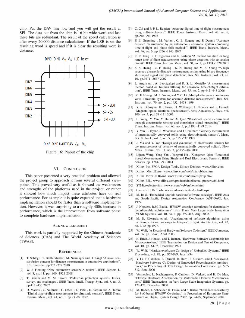
chip. Put the DAV line low and you will get the result atSPI. The data out from the chip is 16 bit wide word and lastthree bits are redundant. The result of the speed calculation isafter every 20,000 distance calculations. If the LSB is set theresulting word is speed and if it is clear the resulting word isdistance.
Figure 16: Pinout of the chip
VI. CONCLUSION
This paper presented a very practical problem and allowedthe project group to approach it from several different view-points. This proved very useful as it showed the weaknessesand strengths of the platforms used in the project, or ratherit showed how much impact these attributes have on realperformance. For example it is quite expected that a hardwareimplementation should be faster than a software implementa-tion. However, it was surprising to a roughly 400x increase inperformance, which is the improvement from software phaseto complete hardware implementation.
ACKNOWLEDGMENT
This work is partially supported by the Chinese Academicof Sciences (CAS) and The World Academy of Sciences(TWAS).
REFERENCES
[1] T. Schlegl , T. Bretterklieber , M. Neumayer and H. Zangl “A novel sen-sor fusion concept for distance measurement in automotive applications”,IEEE Sensors, pp.775 -778 2010
[2] W. J. Fleming “New automotive sensors A review”, IEEE Sensors J.,vol. 8, no. 11, pp.1900 -1921 2008
[3] T. Gandhi and M. M. Trivedi “Pedestrian protection systems: Issues,survey, and challenges”, IEEE Trans. Intell. Transp. Syst., vol. 8, no. 3,pp.413 -430 2007
[4] D. Marioli , C. Narduzzi , C. Offelli , D. Petri , E. Sardini and A. Taroni“Digital time-of-flight measurement for ultrasonic sensors”, IEEE Trans.Instrum. Meas., vol. 41, no. 1, pp.93 -97 1992
[5] C. Cai and P. P. L. Regtien “Accurate digital time-of-flight measurementusing self-interference”, IEEE Trans. Instrum. Meas., vol. 42, no. 6,pp.990 -994 1993
[6] F. E. Gueuning , M. Varlan , C. E. Eugene and P. Dupuis “Accuratedistance measurement by an autonomous ultrasonic system combiningtime-of-flight and phase-shift methods”, IEEE Trans. Instrum. Meas.,vol. 46, no. 6, pp.1236 -1240 1997
[7] C. C. Tong , J. F. Figueroa and E. Barbieri “A method for short or longrange time-of-flight measurements using phase-detection with an analogcircuit”, IEEE Trans. Instrum. Meas., vol. 50, no. 5, pp.1324 -1328 2001
[8] S. S. Huang , C. F. Huang , K. N. Huang and M. S. Young “A highaccuracy ultrasonic distance measurement system using binary frequencyshift-keyed signal and phase detection”, Rev. Sci. Instrum., vol. 73, no.10, pp.3671 -3677 2002
[9] L. Angrisani , A. Baccigalupi and R. S. L. Moriello “A measurementmethod based on Kalman filtering for ultrasonic time-of-flight estima-tion”, IEEE Trans. Instrum. Meas., vol. 55, no. 2, pp.442 -448 2006
[10] C. F. Huang , M. S. Young and Y. C. Li “Multiple-frequency continuouswave ultrasonic system for accurate distance measurement”, Rev. Sci.Instrum., vol. 70, no. 2, pp.1452 -1458 1999
[11] Y. S. Didosyan, H. Hauser, H. Wolfmayr, J. Nicolics and P. Fulmek“Magneto-optical rotational speed sensor”, Sens. Actuators A, Phys., vol.106, no. 3, pp.168 -171 2003
[12] L. Wang, Y. Yan, Y. Hu and X. Qian “Rotational speed measurementthrough electrostatic sensing and correlation signal processing”, IEEETrans. Instrum. Meas., vol. 63, no. 5, pp.1190 -1199 2014
[13] Y. Yan, B. Byrne, S. Woodhead and J. Coulthard “Velocity measurementof pneumatically conveyed solids using electrodynamic sensors”, Meas.Sci. Technol., vol. 6, no. 5, pp.515 -537 1995
[14] J. Ma and Y. Yan “Design and evaluation of electrostatic sensors forthe measurement of velocity of pneumatically conveyed solids”, FlowMeas. Instrum., vol. 11, no. 3, pp.195-204 2000
[15] Lijuan Wang, Yong Yan , Yonghui Hu , Xiangchen Qian “RotationalSpeed Measurement Using Single and Dual Electrostatic Sensors”, IEEESensors, pp. 1784-1793 2014
[16] Xilinx Inc. FPGA Design Tools. Silicon Devices. www.xilinx.com[17] Xilinx. MicroBlaze. www.xilinx.com/tools/microblaze.htm[18] Xilinx Virtex-II Board. www.xilinx.com/univ/xupv2p.html[19] Xilinx FSL. www.xilinx.com/products/intellectual-property/fsl.html[20] STMicroelectronics. www.st.com/web/en/home.html[21] Cadence EDA Tools. www.cadence.com/en/default.aspx[22] M. Imai, “Embedded tutorial: hardware/software codesign”, IEEE Asia
and South Pacific Design Automation Conference (ASP-DAC), Jan.1999.
[23] J. Noguera, R.M. Badia, “HW/SW codesign techniques for dynamicallyreconfigurable architectures” IEEE Trans. Very Large Scale Integration(VLSI) Systems, vol. 10, no. 4, pp. 399-415, Aug. 2002.
[24] M. D. Edwards, et al., “Acceleration of software algorithms usinghardware/software co-design techniques”, J. Syst. Architecture, vol. 42,no. 9/10, pp.1997.
[25] W. Wolf, “A Decade of Hardware/Software Codesign,” IEEE Computer,vol. 36, pp. 38-43, April 2003
[26] R. Ernst, J. Henkel, and T. Benner, “Hardware-Software Cosynthesis forMicrocontrollers,” IEEE Transaction on Design and Test of Computers,vol. 10, pp. 64-75, December 1993
[27] W. Wolf, “Hardware/software Co-design of Embedded Systems,” IEEEProceeding, vol. 82, pp. 967-989, July 1994
[28] Y. Li, T. Callahan, E. Darnell, R. Harr, U. Kurkure, and J. Stockwood,“Hardware-Software Co-Design of Embedded Reconfigurable Architec-tures,” in Proceeding of 37th Design Automation Conference, pp. 507-512, June 2000
[29] Vermeulen, L. Nachtergaele, F. Catthoor, D. Verkest, and H. De Man,“Flexible Hardware Acceleration for Multimedia Oriented Microproces-sors,” IEEE Transactions on Very Large Scale Integration Systems, pp.171-177, December 2000
[30] M. Boden, J. Schneider, K. Feske, and S. Rulke, “Enhanced Reusabilityfor SoC-based HW/SW Co-design,” in Proceeding of Euromicro Sym-posium on Digital System Design 2002, pp. 94-99, September 2002.
(IJACSA) International Journal of Advanced Computer Science and Applications,
Vol. 6, No. 10, 2015
281 | P a g ewww.ijacsa.thesai.org
[31] Kai-Yuan Jan, Chih-Bin Fan, An-Chao Kuo, Wen-Chi Yen, and Youn-Long Lin, “A Platform-based SOC Design Methodology and Its Applica-tion in Image Compression,” Special Issue on HW-SW Codesign for SoC,International Journal of Embedded Systems, Inderscience Publishers,USA. Vol. 1, Issue 1/2, pp. 23-32, 2005.
[32] Chiodo, M. and et al. Hardware-software codesign of embedded sys-tems. In IEEE Micro, 1994.
[33] Ernst, R. and et al. Codesgin of embedded systems: status and trends.In Proceedings of IEEE Design and Test of Computers, 1998.
[34] Gallery, R. and et al. Hardware/software partitioning and simulationwith SystemC. In Proceedings of the 2nd WSEAS ICECSP, 2003.
[35] Hurk, J. and et al. System Level Hardware/Software Co-Design: AnIndustrial Approach, 1997.
[36] De Micheli, G. and et al. Hardware/Software Co-design. In Proceedingsof the IEEE, 1997.
(IJACSA) International Journal of Advanced Computer Science and Applications,
Vol. 6, No. 10, 2015
282 | P a g ewww.ijacsa.thesai.org

![Aalborg Universitet Pathloss Measurements and Modeling for ... · pathloss measurements [4] In [5], measurements in mountainous environments are fit using a log-distance model with](https://img.pdfslide.us/doc/110x75/5e8fddb8019cac093f1a675b/aalborg-universitet-pathloss-measurements-and-modeling-for-pathloss-measurements.jpg)