Embed Size (px)
Citation preview

September 2013 Doc ID 7393 Rev 9 1/31
1
VNB14NV04, VND14NV04VND14NV04-1, VNS14NV04
"OMNIFET II"fully autoprotected Power MOSFET
Features
■ Linear current limitation
■ Thermal shutdown
■ Short circuit protection
■ Integrated clamp
■ Low current drawn from input pin
■ Diagnostic feedback through input pin
■ ESD protection
■ Direct access to the gate of the Power MOSFET (analog driving)
■ Compatible with standard Power MOSFET
DescriptionThe VNB14NV04, VND14NV04, VND14NV04-1 and VNS14NV04 are monolithic devices made using STMicroelectronics VIPower™ M0 technology, intended for replacement of standard power MOSFETS in DC to 50 KHz applications. Built-in thermal shutdown, linear current limitation and overvoltage clamp protect the chip in harsh environments.
Fault feedback can be detected by monitoring the voltage at the input pin.
TYPE RDS(on) Ilim Vclamp
VNB14NV04 VND14NV04VND14NV04-1
VNS14NV04
35 mΩ 12 A 40 V
1
3 32
1
13
TO-252 (DPAK) TO-251 (IPAK)
SO-8 D2PAK
Table 1. Device summary
Package Tube Tube (lead free) Tape and reel Tape and reel (lead free)
D2PAK VNB14NV04 VNB14NV04-E VNB14NV0413TR VNB14NV04TR-E
TO-252 (DPAK) VND14NV04 VND14NV04-E VND14NV0413TR VND14NV04TR-E
TO-251 (IPAK) VND14NV04-1 VND14NV04-1-E - -
SO-8 VNS14NV04 - - -
www.st.com

Contents VNB14NV04, VND14NV04, VND14NV04-1, VNS14NV04
2/31 Doc ID 7393 Rev 9
Contents
1 Block diagram . . . . . . . . . . . . . . . . . . . . . . . . . . . . . . . . . . . . . . . . . . . . . . 5
2 Electrical specification . . . . . . . . . . . . . . . . . . . . . . . . . . . . . . . . . . . . . . . 6
2.1 Absolute maximum rating . . . . . . . . . . . . . . . . . . . . . . . . . . . . . . . . . . . . . . 6
2.2 Thermal data . . . . . . . . . . . . . . . . . . . . . . . . . . . . . . . . . . . . . . . . . . . . . . . 7
2.3 Electrical characteristics . . . . . . . . . . . . . . . . . . . . . . . . . . . . . . . . . . . . . . . 7
3 Protection features . . . . . . . . . . . . . . . . . . . . . . . . . . . . . . . . . . . . . . . . . . 9
4 Package thermal data . . . . . . . . . . . . . . . . . . . . . . . . . . . . . . . . . . . . . . . 18
4.1 DPAK thermal data . . . . . . . . . . . . . . . . . . . . . . . . . . . . . . . . . . . . . . . . . . 18
4.2 SO-8 thermal data . . . . . . . . . . . . . . . . . . . . . . . . . . . . . . . . . . . . . . . . . . 20
4.3 D2PAK thermal data . . . . . . . . . . . . . . . . . . . . . . . . . . . . . . . . . . . . . . . . . 21
5 Package information . . . . . . . . . . . . . . . . . . . . . . . . . . . . . . . . . . . . . . . . 24
5.1 ECOPACK® . . . . . . . . . . . . . . . . . . . . . . . . . . . . . . . . . . . . . . . . . . . . . . . 24
5.2 TO-251 (IPAK) mechanical data . . . . . . . . . . . . . . . . . . . . . . . . . . . . . . . . 24
5.3 D2PAK mechanical data . . . . . . . . . . . . . . . . . . . . . . . . . . . . . . . . . . . . . . 25
5.4 TO-252 (DPAK) mechanical data . . . . . . . . . . . . . . . . . . . . . . . . . . . . . . . 27
5.5 SO-8 mechanical data . . . . . . . . . . . . . . . . . . . . . . . . . . . . . . . . . . . . . . . 28
6 Revision history . . . . . . . . . . . . . . . . . . . . . . . . . . . . . . . . . . . . . . . . . . . 30

VNB14NV04, VND14NV04, VND14NV04-1, VNS14NV04 List of tables
Doc ID 7393 Rev 9 3/31
List of tables
Table 1. Device summary . . . . . . . . . . . . . . . . . . . . . . . . . . . . . . . . . . . . . . . . . . . . . . . . . . . . . . . . . . 1Table 2. Absolute maximum rating . . . . . . . . . . . . . . . . . . . . . . . . . . . . . . . . . . . . . . . . . . . . . . . . . . . 6Table 3. Thermal data. . . . . . . . . . . . . . . . . . . . . . . . . . . . . . . . . . . . . . . . . . . . . . . . . . . . . . . . . . . . . 7Table 4. Electrical characteristics . . . . . . . . . . . . . . . . . . . . . . . . . . . . . . . . . . . . . . . . . . . . . . . . . . . . 7Table 5. DPAK thermal parameter . . . . . . . . . . . . . . . . . . . . . . . . . . . . . . . . . . . . . . . . . . . . . . . . . . 19Table 6. D2PAK thermal parameter . . . . . . . . . . . . . . . . . . . . . . . . . . . . . . . . . . . . . . . . . . . . . . . . . 22Table 7. TO-251 (IPAK) mechanical data. . . . . . . . . . . . . . . . . . . . . . . . . . . . . . . . . . . . . . . . . . . . . 24Table 8. D2PAK mechanical data . . . . . . . . . . . . . . . . . . . . . . . . . . . . . . . . . . . . . . . . . . . . . . . . . . . 26Table 9. TO-252 (DPAK) mechanical data . . . . . . . . . . . . . . . . . . . . . . . . . . . . . . . . . . . . . . . . . . . . 27Table 10. SO-8 mechanical data . . . . . . . . . . . . . . . . . . . . . . . . . . . . . . . . . . . . . . . . . . . . . . . . . . . . 28Table 11. Document revision history . . . . . . . . . . . . . . . . . . . . . . . . . . . . . . . . . . . . . . . . . . . . . . . . . 30

List of figures VNB14NV04, VND14NV04, VND14NV04-1, VNS14NV04
4/31 Doc ID 7393 Rev 9
List of figures
Figure 1. Block diagram . . . . . . . . . . . . . . . . . . . . . . . . . . . . . . . . . . . . . . . . . . . . . . . . . . . . . . . . . . . . 5Figure 2. Current and voltage conventions . . . . . . . . . . . . . . . . . . . . . . . . . . . . . . . . . . . . . . . . . . . . . 6Figure 3. Switching time test circuit for resistive load . . . . . . . . . . . . . . . . . . . . . . . . . . . . . . . . . . . . 10Figure 4. Test circuit for diode recovery times . . . . . . . . . . . . . . . . . . . . . . . . . . . . . . . . . . . . . . . . . . 10Figure 5. Unclamped inductive load test circuits . . . . . . . . . . . . . . . . . . . . . . . . . . . . . . . . . . . . . . . . 11Figure 6. Unclamped inductive waveforms . . . . . . . . . . . . . . . . . . . . . . . . . . . . . . . . . . . . . . . . . . . . 11Figure 7. Input charge test circuit. . . . . . . . . . . . . . . . . . . . . . . . . . . . . . . . . . . . . . . . . . . . . . . . . . . . 11Figure 8. Source-drain diode forward characteristics . . . . . . . . . . . . . . . . . . . . . . . . . . . . . . . . . . . . 12Figure 9. Static drain source on resistance . . . . . . . . . . . . . . . . . . . . . . . . . . . . . . . . . . . . . . . . . . . . 12Figure 10. Derating curve . . . . . . . . . . . . . . . . . . . . . . . . . . . . . . . . . . . . . . . . . . . . . . . . . . . . . . . . . . 12Figure 11. Static drain-source on resistance vs. input voltage (part 1/2) . . . . . . . . . . . . . . . . . . . . . . . 12Figure 12. Static drain-source on resistance vs. input voltage (part 2/2) . . . . . . . . . . . . . . . . . . . . . . . 12Figure 13. Transconductance . . . . . . . . . . . . . . . . . . . . . . . . . . . . . . . . . . . . . . . . . . . . . . . . . . . . . . . 12Figure 14. Static drain-source on resistance vs. id . . . . . . . . . . . . . . . . . . . . . . . . . . . . . . . . . . . . . . . 13Figure 15. Transfer characteristics . . . . . . . . . . . . . . . . . . . . . . . . . . . . . . . . . . . . . . . . . . . . . . . . . . . 13Figure 16. Turn-on current slope (part 1/2) . . . . . . . . . . . . . . . . . . . . . . . . . . . . . . . . . . . . . . . . . . . . . 13Figure 17. Turn-on current slope (part 2/2) . . . . . . . . . . . . . . . . . . . . . . . . . . . . . . . . . . . . . . . . . . . . . 13Figure 18. Input voltage vs. input charge. . . . . . . . . . . . . . . . . . . . . . . . . . . . . . . . . . . . . . . . . . . . . . . 13Figure 19. Turn-off drain source voltage slope (part 1/2). . . . . . . . . . . . . . . . . . . . . . . . . . . . . . . . . . . 13Figure 20. Turn-off drain source voltage slope (part 2/2). . . . . . . . . . . . . . . . . . . . . . . . . . . . . . . . . . . 14Figure 21. Capacitance variations . . . . . . . . . . . . . . . . . . . . . . . . . . . . . . . . . . . . . . . . . . . . . . . . . . . . 14Figure 22. Switching time resistive load (part 1/2) . . . . . . . . . . . . . . . . . . . . . . . . . . . . . . . . . . . . . . . . 14Figure 23. Switching time resistive load (part 2/2) . . . . . . . . . . . . . . . . . . . . . . . . . . . . . . . . . . . . . . . . 14Figure 24. Output characteristics . . . . . . . . . . . . . . . . . . . . . . . . . . . . . . . . . . . . . . . . . . . . . . . . . . . . . 14Figure 25. Normalized on resistance vs. temperature . . . . . . . . . . . . . . . . . . . . . . . . . . . . . . . . . . . . . 14Figure 26. Normalized input threshold voltage vs. temperature . . . . . . . . . . . . . . . . . . . . . . . . . . . . . 15Figure 27. Current limit vs. junction temperatures . . . . . . . . . . . . . . . . . . . . . . . . . . . . . . . . . . . . . . . . 15Figure 28. Step response current limit . . . . . . . . . . . . . . . . . . . . . . . . . . . . . . . . . . . . . . . . . . . . . . . . . 15Figure 29. DPAK maximum turn-off current versus load inductance . . . . . . . . . . . . . . . . . . . . . . . . . . 16Figure 30. DPAK demagnetization. . . . . . . . . . . . . . . . . . . . . . . . . . . . . . . . . . . . . . . . . . . . . . . . . . . . 16Figure 31. D2PAK maximum turn-off current versus load inductance . . . . . . . . . . . . . . . . . . . . . . . . . 17Figure 32. D2PAK demagnetization . . . . . . . . . . . . . . . . . . . . . . . . . . . . . . . . . . . . . . . . . . . . . . . . . . . 17Figure 33. DPAK PC board(1) . . . . . . . . . . . . . . . . . . . . . . . . . . . . . . . . . . . . . . . . . . . . . . . . . . . . . . . 18Figure 34. DPAK Rthj-amb vs PCB copper area in open box free air condition. . . . . . . . . . . . . . . . . . . 18Figure 35. DPAK thermal impedance junction ambient single pulse . . . . . . . . . . . . . . . . . . . . . . . . . . 19Figure 36. Thermal fitting model of an OMNIFET II in DPAK. . . . . . . . . . . . . . . . . . . . . . . . . . . . . . . . 19Figure 37. SO-8 PC board(1) . . . . . . . . . . . . . . . . . . . . . . . . . . . . . . . . . . . . . . . . . . . . . . . . . . . . . . . . 20Figure 38. SO-8 Rthj-amb vs PCB copper area in open box free air condition . . . . . . . . . . . . . . . . . . . 20Figure 39. D2PAK PC board(1). . . . . . . . . . . . . . . . . . . . . . . . . . . . . . . . . . . . . . . . . . . . . . . . . . . . . . . 21Figure 40. D2PAK Rthj-amb vs PCB copper area in open box free air condition . . . . . . . . . . . . . . . . . . 21Figure 41. D2PAK thermal impedance junction ambient single pulse . . . . . . . . . . . . . . . . . . . . . . . . . 22Figure 42. Thermal fitting model of an OMNIFET II in D2PAK. . . . . . . . . . . . . . . . . . . . . . . . . . . . . . . 22Figure 43. TO-251 (IPAK) package dimension . . . . . . . . . . . . . . . . . . . . . . . . . . . . . . . . . . . . . . . . . . 24Figure 44. D2PAK package dimension . . . . . . . . . . . . . . . . . . . . . . . . . . . . . . . . . . . . . . . . . . . . . . . . 25Figure 45. TO-252 (DPAK) package dimension . . . . . . . . . . . . . . . . . . . . . . . . . . . . . . . . . . . . . . . . . 27Figure 46. SO-8 package dimension . . . . . . . . . . . . . . . . . . . . . . . . . . . . . . . . . . . . . . . . . . . . . . . . . . 28

VNB14NV04, VND14NV04, VND14NV04-1, VNS14NV04 Block diagram
Doc ID 7393 Rev 9 5/31
1 Block diagram
Figure 1. Block diagram
Electrical specification VNB14NV04, VND14NV04, VND14NV04-1, VNS14NV04
6/31 Doc ID 7393 Rev 9
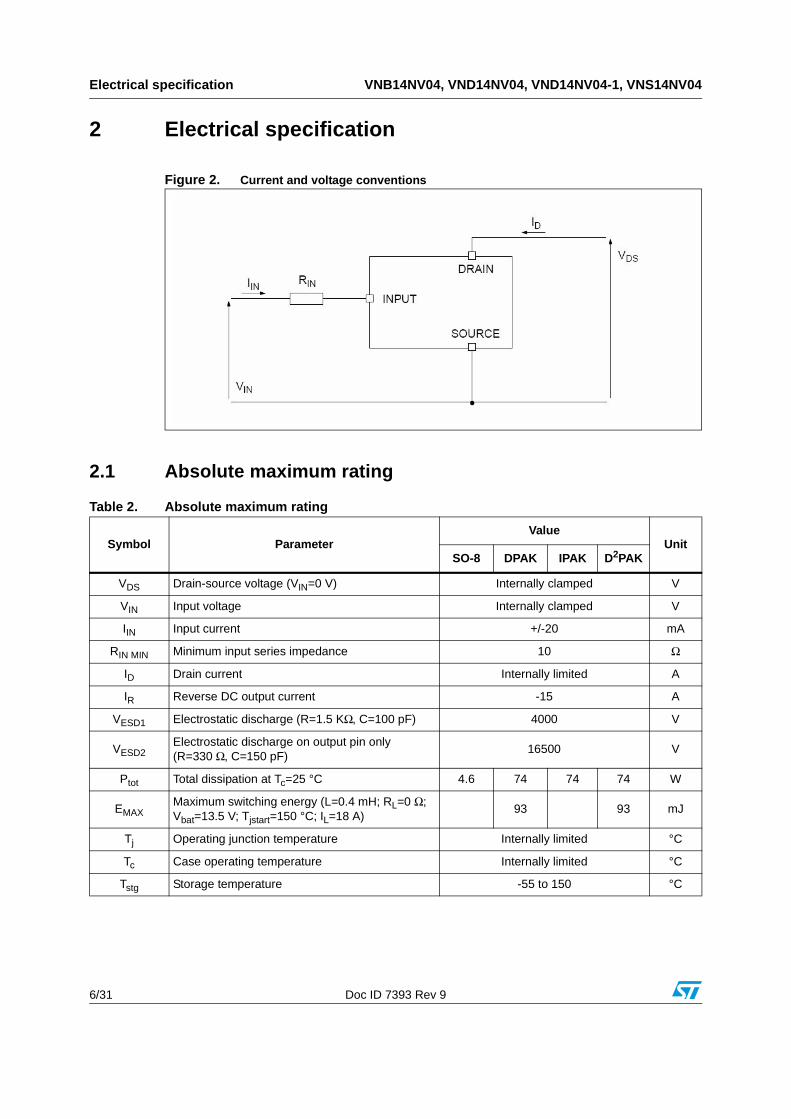
2 Electrical specification
Figure 2. Current and voltage conventions
2.1 Absolute maximum rating
Table 2. Absolute maximum rating
Symbol ParameterValue
UnitSO-8 DPAK IPAK D2PAK
VDS Drain-source voltage (VIN=0 V) Internally clamped V
VIN Input voltage Internally clamped V
IIN Input current +/-20 mA
RIN MIN Minimum input series impedance 10 Ω
ID Drain current Internally limited A
IR Reverse DC output current -15 A
VESD1 Electrostatic discharge (R=1.5 KΩ, C=100 pF) 4000 V
VESD2 Electrostatic discharge on output pin only (R=330 Ω, C=150 pF)
16500 V
Ptot Total dissipation at Tc=25 °C 4.6 74 74 74 W
EMAX Maximum switching energy (L=0.4 mH; RL=0 Ω; Vbat=13.5 V; Tjstart=150 °C; IL=18 A)
93 93 mJ
Tj Operating junction temperature Internally limited °C
Tc Case operating temperature Internally limited °C
Tstg Storage temperature -55 to 150 °C

VNB14NV04, VND14NV04, VND14NV04-1, VNS14NV04 Electrical specification
Doc ID 7393 Rev 9 7/31
2.2 Thermal data
2.3 Electrical characteristics-40 < Tj < 150 °C unless otherwise specified.
Table 3. Thermal data
Symbol Parameter Value
Unit SO-8 DPAK IPAK D2PAK
Rthj-case Thermal resistance junction-case max 1.7 1.7 1.7 °C/W
Rthj-lead Thermal resistance junction-lead max 27 °C/W
Rthj-amb Thermal resistance junction-ambient max 90(1) 65(1) 102 52(1) °C/W
1. When mounted on a standard single-sided FR4 board with 0.5 cm2 of Cu (at least 35 µm thick) connected to all DRAIN pins. Horizontal mounting and no artificial air flow.
Table 4. Electrical characteristics
Symbol Parameter Test Conditions Min Typ Max Unit
Off
VCLAMP Drain-source clamp voltage VIN=0 V; ID=7 A 40 45 55 V
VCLTH
Drain-source clamp threshold voltage
VIN=0 V; ID=2 mA 36 V
VINTH Input threshold voltage VDS=VIN; ID=1 mA 0.5 2.5 V
IISS Supply current from input pin VDS=0 V; VIN=5 V 100 150 µA
VINCL Input-source clamp voltage IIN=1 mAIIN=-1 mA
6-1.0
6.8 8-0.3
V
IDSS Zero input voltage drain current (VIN=0 V)
VDS=13 V; VIN=0 V; Tj=25 °C VDS=25 V; VIN=0 V
3075
µA
On
RDS(on) Static drain-source on resistanceVin = 5 V ID = 7 A Tj = 25 °CVin = 5 V ID = 7 A
3570
mΩ
Dynamic (Tj=25°C, unless otherwise specified)
gfs (1) Forward transconductance VDD = 13 V ID = 7 A 18 S
Coss Output capacitance VDS = 13 V f = 1 MHz VIN = 0 V 400 pF
Switching
td(on) Turn-on delay timeVDD = 15 V ID = 7 A
Vgen = 5 V Rgen = RIN MIN =10 Ω(see Figure 3)
80 250 ns
tr Rise time 350 1000 ns
td(off) Turn-off delay time 450 1350 ns
tf Fall time 150 500 ns

Electrical specification VNB14NV04, VND14NV04, VND14NV04-1, VNS14NV04
8/31 Doc ID 7393 Rev 9
td(on) Turn-on delay timeVDD = 15 V Id = 7 AVgen = 5 V Rgen = 2.2 KΩ(see Figure 3)
1.5 4.5 µs
tr Rise time 9.7 30.0 µs
td(off) Turn-off delay time 25.0 µs
tf Fall time 10.2 30.0 µs
(di/dt)on Turn-on current slopeVDD = 15 V ID = 7 AVgen = 5 V Rgen = RIN MIN =10 Ω
16 A/µs
Qi Total input chargeVDD = 12 V ID = 7 A Vin = 5 V;Igen = 2.13 mA (see Figure 7)
36.8 nC
Source drain diode
VSD(1) Forward on voltage ISD = 7 A Vin = 0 V 0.8 V
trr Reverse recovery time ISD = 7 A; di/dt = 40 A/µsVDD = 30 V L = 200 µH(see test circuit, Figure 4)
300 ns
Qrr Reverse recovery charge 0.8 µC
IRRM Reverse recovery current 5 A
Protection
Ilim Drain current limit VIN = 5 V; VDS = 13 V 12 18 24 A
tdlim Step response current limit VIN = 5 V; VDS = 13 V 45 µs
Tjsh Over temperature shutdown 150 175 200 °C
Tjrs Over temperature reset 135 °C
Igf Fault sink current VIN = 5 V; VDS = 13 V; Tj = Tjsh 10 15 20 mA
Eas Single pulse avalanche energy
starting Tj = 25 °C; VDD = 24 VVIN = 5 V; Rgen = RIN MIN = 10 Ω;L = 24 mH (see Figure 5 and Figure 6)
400 mJ
1. Pulsed: Pulse duration = 300 µs, duty cycle 1.5 %
Table 4. Electrical characteristics (continued)
Symbol Parameter Test Conditions Min Typ Max Unit

VNB14NV04, VND14NV04, VND14NV04-1, VNS14NV04 Protection features
Doc ID 7393 Rev 9 9/31
3 Protection features
During normal operation, the input pin is electrically connected to the gate of the internal power MOSFET through a low impedance path.
The device then behaves like a standard power MOSFET and can be used as a switch from DC up to 50 KHz. The only difference from the user’s standpoint is that a small DC current IISS (typ. 100 µA) flows into the input pin in order to supply the internal circuitry.
The device integrates:
● Overvoltage clamp protection: internally set at 45 V, along with the rugged avalanche characteristics of the Power MOSFET stage give this device unrivalled ruggedness and energy handling capability. This feature is mainly important when driving inductive loads.
● Linear current limiter circuit: limits the drain current ID to Ilim whatever the input pin voltages. When the current limiter is active, the device operates in the linear region, so power dissipation may exceed the capability of the heatsink. Both case and junction temperatures increase, and if this phase lasts long enough, junction temperature may reach the over temperature threshold Tjsh.
● Over temperature and short circuit protection: these are based on sensing the chip temperature and are not dependent on the input voltage. The location of the sensing element on the chip in the power stage area ensures fast, accurate detection of the junction temperature. Over temperature cutout occurs in the range 150 to 190 °C, a typical value being 170 °C. The device is automatically restarted when the chip temperature falls of about 15 °C below shutdown temperature.
● Status feedback: in the case of an over temperature fault condition (Tj > Tjsh), the device tries to sink a diagnostic current Igf through the input pin in order to indicate fault condition. If driven from a low impedance source, this current may be used in order to warn the control circuit of a device shutdown. If the drive impedance is high enough so that the input pin driver is not able to supply the current Igf, the input pin will fall to 0 V. This will not however affect the device operation: no requirement is put on the current capability of the input pin driver except to be able to supply the normal operation drive current IISS.
Additional features of this device are ESD protection according to the Human Body model and the ability to be driven from a TTL Logic circuit.

Protection features VNB14NV04, VND14NV04, VND14NV04-1, VNS14NV04
10/31 Doc ID 7393 Rev 9
Figure 3. Switching time test circuit for resistive load
Figure 4. Test circuit for diode recovery times

VNB14NV04, VND14NV04, VND14NV04-1, VNS14NV04 Protection features
Doc ID 7393 Rev 9 11/31
Figure 5. Unclamped inductive load test circuits
Figure 6. Unclamped inductive waveforms
Figure 7. Input charge test circuit

Protection features VNB14NV04, VND14NV04, VND14NV04-1, VNS14NV04
12/31 Doc ID 7393 Rev 9
Figure 8. Source-drain diode forward characteristics
Figure 9. Static drain source on resistance
Figure 10. Derating curve Figure 11. Static drain-source on resistance vs. input voltage (part 1/2)
Figure 12. Static drain-source on resistance vs. input voltage (part 2/2)
Figure 13. Transconductance

VNB14NV04, VND14NV04, VND14NV04-1, VNS14NV04 Protection features
Doc ID 7393 Rev 9 13/31
Figure 14. Static drain-source on resistance vs. id
Figure 15. Transfer characteristics
Figure 16. Turn-on current slope (part 1/2) Figure 17. Turn-on current slope (part 2/2)
Figure 18. Input voltage vs. input charge Figure 19. Turn-off drain source voltage slope (part 1/2)

Protection features VNB14NV04, VND14NV04, VND14NV04-1, VNS14NV04
14/31 Doc ID 7393 Rev 9
Figure 20. Turn-off drain source voltage slope (part 2/2)
Figure 21. Capacitance variations
Figure 22. Switching time resistive load (part 1/2)
Figure 23. Switching time resistive load (part 2/2)
Figure 24. Output characteristics Figure 25. Normalized on resistance vs. temperature

VNB14NV04, VND14NV04, VND14NV04-1, VNS14NV04 Protection features
Doc ID 7393 Rev 9 15/31
Figure 26. Normalized input threshold voltage vs. temperature
Figure 27. Current limit vs. junction temperatures
Figure 28. Step response current limit

Protection features VNB14NV04, VND14NV04, VND14NV04-1, VNS14NV04
16/31 Doc ID 7393 Rev 9
Figure 29. DPAK maximum turn-off current versus load inductance
Legend:
A= Single pulse at TJstart=150ºC
B= Repetitive pulse at TJstart=100ºC
C= Repetitive pulse at TJstart=125ºC
Conditions:
VCC=13.5 V
Values are generated with RL=0Ω
In case of repetitive pulses, Tjstart (at beginning of each demagnetization) of every pulse must not exceed the temperature specified above for curves B and C.
Figure 30. DPAK demagnetization

VNB14NV04, VND14NV04, VND14NV04-1, VNS14NV04 Protection features
Doc ID 7393 Rev 9 17/31
Figure 31. D2PAK maximum turn-off current versus load inductance
Legend:
A= Single pulse at TJstart=150ºC
B= Repetitive pulse at TJstart=100ºC
C= Repetitive pulse at TJstart=125ºC
Conditions:
VCC=13.5 V
Values are generated with RL=0Ω
In case of repetitive pulses, Tjstart (at beginning of each demagnetization) of every pulse must not exceed the temperature specified above for curves B and C.
Figure 32. D2PAK demagnetization

Package thermal data VNB14NV04, VND14NV04, VND14NV04-1, VNS14NV04
18/31 Doc ID 7393 Rev 9
4 Package thermal data
4.1 DPAK thermal data
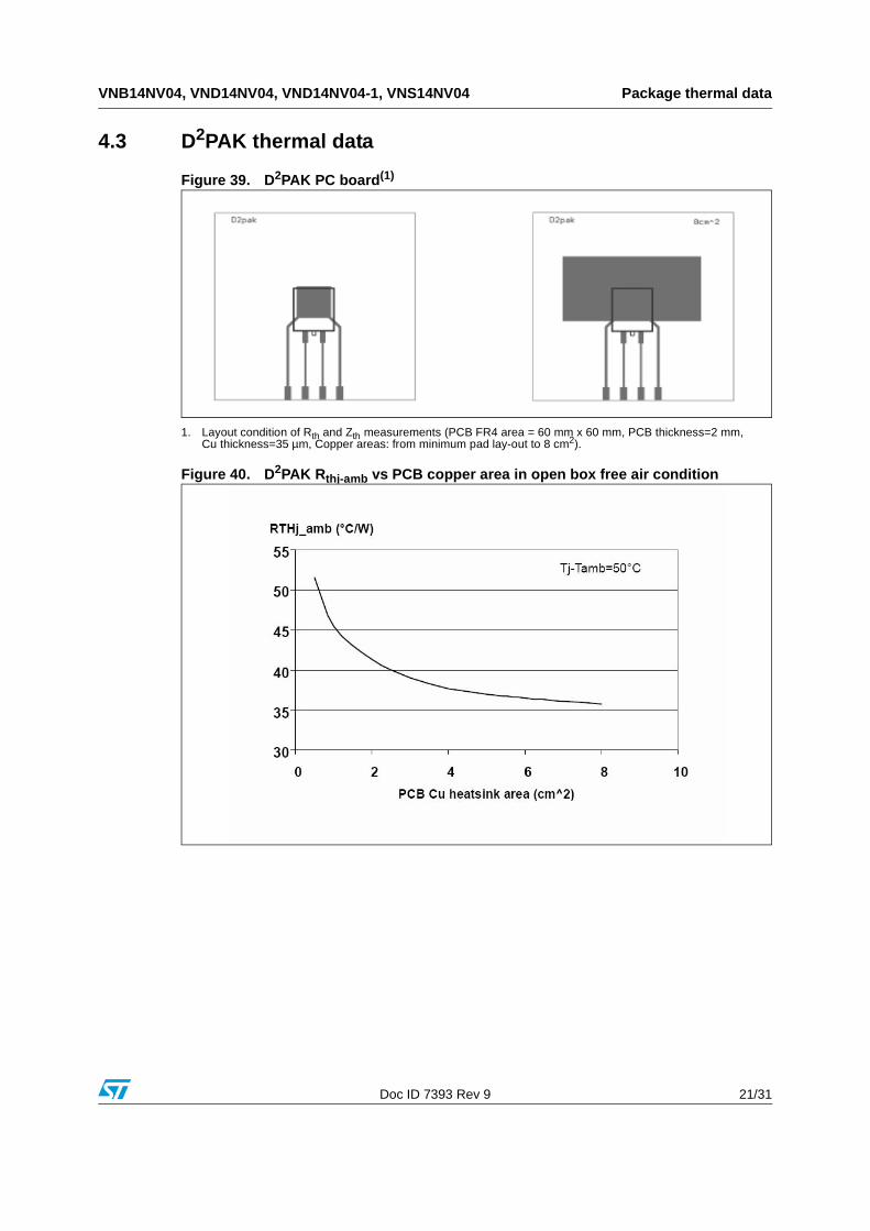
Figure 33. DPAK PC board(1)
1. Layout condition of Rth and Zth measurements (PCB FR4 area = 60 mm x 60 mm, PCB thickness=2 mm, Cu thickness=35 µm, Copper areas: from minimum pad lay-out to 8 cm2).
Figure 34. DPAK Rthj-amb vs PCB copper area in open box free air condition

VNB14NV04, VND14NV04, VND14NV04-1, VNS14NV04 Package thermal data
Doc ID 7393 Rev 9 19/31
Figure 35. DPAK thermal impedance junction ambient single pulse
Figure 36. Thermal fitting model of an OMNIFET II in DPAK
Pulse calculation formula
where
Table 5. DPAK thermal parameter
Area/island(cm2) Footprint 6
R1 (°C/W) 0.1
R2 (°C/W) 0.35
R3 ( °C/W) 1.20
R4 (°C/W) 2
R5 (°C/W) 15
R6 (°C/W) 61 24
C1 (W.s/°C) 0.0006
C2 (W.s/°C) 0.0021
C3 (W.s/°C) 0.05
ZTHδ RTH δ⋅ ZTHtp 1 δ–( )+=
δ tp T⁄=

Package thermal data VNB14NV04, VND14NV04, VND14NV04-1, VNS14NV04
20/31 Doc ID 7393 Rev 9
4.2 SO-8 thermal data
Figure 37. SO-8 PC board(1)
1. Layout condition of Rth and Zth measurements (PCB FR4 area = 58 mm x 58 mm, PCB thickness=2 mm, Cu thickness=35 µm, Copper areas: 0.14 cm2, 0.6 cm2, 1.6 cm2).
Figure 38. SO-8 Rthj-amb vs PCB copper area in open box free air condition
C4 (W.s/°C) 0.3
C5 (W.s/°C) 0.45
C6 (W.s/°C) 0.8 5
Table 5. DPAK thermal parameter (continued)
Area/island(cm2) Footprint 6
VNB14NV04, VND14NV04, VND14NV04-1, VNS14NV04 Package thermal data
Doc ID 7393 Rev 9 21/31
4.3 D2PAK thermal data
Figure 39. D2PAK PC board(1)
1. Layout condition of Rth and Zth measurements (PCB FR4 area = 60 mm x 60 mm, PCB thickness=2 mm, Cu thickness=35 µm, Copper areas: from minimum pad lay-out to 8 cm2).
Figure 40. D2PAK Rthj-amb vs PCB copper area in open box free air condition

Package thermal data VNB14NV04, VND14NV04, VND14NV04-1, VNS14NV04
22/31 Doc ID 7393 Rev 9
Figure 41. D2PAK thermal impedance junction ambient single pulse
Figure 42. Thermal fitting model of an OMNIFET II in D2PAK
Pulse calculation formula
where
Table 6. D2PAK thermal parameter
Area/island(cm2) Footprint 6
R1 (°C/W) 0.1
R2 (°C/W) 0.35
R3 ( °C/W) 0.3
R4 (°C/W) 4
R5 (°C/W) 9
R6 (°C/W) 37 22
C1 (W.s/°C) 0.0006
C2 (W.s/°C) 2.10E-03
ZTHδ RTH δ⋅ ZTHtp 1 δ–( )+=
δ tp T⁄=

VNB14NV04, VND14NV04, VND14NV04-1, VNS14NV04 Package thermal data
Doc ID 7393 Rev 9 23/31
C3 (W.s/°C) 8.00E-02
C4 (W.s/°C) 0.45
C5 (W.s/°C) 2
C6 (W.s/°C) 3 5
Table 6. D2PAK thermal parameter (continued)
Area/island(cm2) Footprint 6

Package information VNB14NV04, VND14NV04, VND14NV04-1, VNS14NV04
24/31 Doc ID 7393 Rev 9
5 Package information
5.1 ECOPACK®
In order to meet environmental requirements, ST offers these devices in different grades of ECOPACK® packages, depending on their level of environmental compliance. ECOPACK®
specifications, grade definitions and product status are available at: www.st.com.
ECOPACK® is an ST trademark.
5.2 TO-251 (IPAK) mechanical data
Figure 43. TO-251 (IPAK) package dimension
Table 7. TO-251 (IPAK) mechanical data
Dim.Millimeters
Min. Typ. Max.
A 2.2 2.4
A1 0.9 1.1
A3 0.7 1.3
B 0.64 0.9
B2 5.2 5.4
VNB14NV04, VND14NV04, VND14NV04-1, VNS14NV04 Package information
Doc ID 7393 Rev 9 25/31
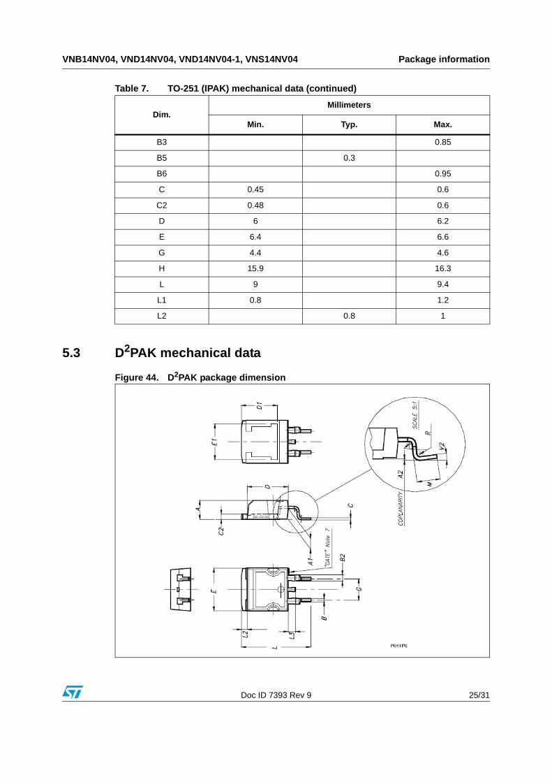
5.3 D2PAK mechanical data
Figure 44. D2PAK package dimension
B3 0.85
B5 0.3
B6 0.95
C 0.45 0.6
C2 0.48 0.6
D 6 6.2
E 6.4 6.6
G 4.4 4.6
H 15.9 16.3
L 9 9.4
L1 0.8 1.2
L2 0.8 1
Table 7. TO-251 (IPAK) mechanical data (continued)
Dim.Millimeters
Min. Typ. Max.

Package information VNB14NV04, VND14NV04, VND14NV04-1, VNS14NV04
26/31 Doc ID 7393 Rev 9
Table 8. D2PAK mechanical data
Dim.Millimeters
Min. Typ. Max.
A 4.4 4.6
A1 2.49 2.69
A2 0.03 0.23
B 0.7 0.93
B2 1.14 1.7
C 0.45 0.6
C2 1.23 1.36
D 8.95 9.35
D1 8
E 10 10.4
E1 8.5
G 4.88 5.28
L 15 15.85
L2 1.27 1.4
L3 1.4 1.75
M 2.4 3.2
R 0.4
V2 0° 8°

VNB14NV04, VND14NV04, VND14NV04-1, VNS14NV04 Package information
Doc ID 7393 Rev 9 27/31
5.4 TO-252 (DPAK) mechanical data
Figure 45. TO-252 (DPAK) package dimension
Table 9. TO-252 (DPAK) mechanical data
Dim.Millimeters
Min. Typ. Max.
A 2.20 2.40
A1 0.90 1.10
A2 0.03 0.23
B 0.64 0.90
B2 5.20 5.40
C 0.45 0.6
C2 0.48 0.6
D 6 6.20
D1 5.1
E 6.4 6.6
E1 4.7
e 2.28
G 4.4 4.6
H 9.35 10.1
L2 0.8

Package information VNB14NV04, VND14NV04, VND14NV04-1, VNS14NV04
28/31 Doc ID 7393 Rev 9
5.5 SO-8 mechanical data
Figure 46. SO-8 package dimension
L4 0.6 1
R 0.2
V2 0° 8°
Package weight Gr. 0.29
Table 9. TO-252 (DPAK) mechanical data (continued)
Dim.Millimeters
Min. Typ. Max.
Table 10. SO-8 mechanical data
Dim.Millimeters
Min. Typ. Max.
A 1.75 2.40
a1 0.25 0.1
a2 1.65
b 0.85 0.35
b1 0.25 0.19

VNB14NV04, VND14NV04, VND14NV04-1, VNS14NV04 Package information
Doc ID 7393 Rev 9 29/31
C 0.5 0.25
c1 45
D 5 4.8
E 6.2 5.8
e 1.27
e3 3.81
F 4 3.8
L 1.27 0.4
M 0.6
F 8
Table 10. SO-8 mechanical data (continued)
Dim.Millimeters
Min. Typ. Max.

Revision history VNB14NV04, VND14NV04, VND14NV04-1, VNS14NV04
30/31 Doc ID 7393 Rev 9
6 Revision history
Table 11. Document revision history
Date Revision Changes
21-Jun-2004 6 Initial release.
03-Apr-2009 7Document reformatted.Added Table 1: Device summary on page 1.Updated Section 5: Package information on page 24
06-Apr-2010 8
Added part number VNS14NV04.Added SO-8 package:
– Updated Table 1: Device summary– Updated Table 2: Absolute maximum rating– Updated Table 3: Thermal data
– Updated Chapter 4: Package thermal data– Updated Chapter 5: Package information
20-Sep-2013 9 Updated Disclaimer.

VNB14NV04, VND14NV04, VND14NV04-1, VNS14NV04
Doc ID 7393 Rev 9 31/31
Please Read Carefully:
Information in this document is provided solely in connection with ST products. STMicroelectronics NV and its subsidiaries (“ST”) reserve theright to make changes, corrections, modifications or improvements, to this document, and the products and services described herein at anytime, without notice.
All ST products are sold pursuant to ST’s terms and conditions of sale.
Purchasers are solely responsible for the choice, selection and use of the ST products and services described herein, and ST assumes noliability whatsoever relating to the choice, selection or use of the ST products and services described herein.
No license, express or implied, by estoppel or otherwise, to any intellectual property rights is granted under this document. If any part of thisdocument refers to any third party products or services it shall not be deemed a license grant by ST for the use of such third party productsor services, or any intellectual property contained therein or considered as a warranty covering the use in any manner whatsoever of suchthird party products or services or any intellectual property contained therein.
UNLESS OTHERWISE SET FORTH IN ST’S TERMS AND CONDITIONS OF SALE ST DISCLAIMS ANY EXPRESS OR IMPLIEDWARRANTY WITH RESPECT TO THE USE AND/OR SALE OF ST PRODUCTS INCLUDING WITHOUT LIMITATION IMPLIEDWARRANTIES OF MERCHANTABILITY, FITNESS FOR A PARTICULAR PURPOSE (AND THEIR EQUIVALENTS UNDER THE LAWSOF ANY JURISDICTION), OR INFRINGEMENT OF ANY PATENT, COPYRIGHT OR OTHER INTELLECTUAL PROPERTY RIGHT.
ST PRODUCTS ARE NOT DESIGNED OR AUTHORIZED FOR USE IN: (A) SAFETY CRITICAL APPLICATIONS SUCH AS LIFESUPPORTING, ACTIVE IMPLANTED DEVICES OR SYSTEMS WITH PRODUCT FUNCTIONAL SAFETY REQUIREMENTS; (B)AERONAUTIC APPLICATIONS; (C) AUTOMOTIVE APPLICATIONS OR ENVIRONMENTS, AND/OR (D) AEROSPACE APPLICATIONSOR ENVIRONMENTS. WHERE ST PRODUCTS ARE NOT DESIGNED FOR SUCH USE, THE PURCHASER SHALL USE PRODUCTS ATPURCHASER’S SOLE RISK, EVEN IF ST HAS BEEN INFORMED IN WRITING OF SUCH USAGE, UNLESS A PRODUCT ISEXPRESSLY DESIGNATED BY ST AS BEING INTENDED FOR “AUTOMOTIVE, AUTOMOTIVE SAFETY OR MEDICAL” INDUSTRYDOMAINS ACCORDING TO ST PRODUCT DESIGN SPECIFICATIONS. PRODUCTS FORMALLY ESCC, QML OR JAN QUALIFIED AREDEEMED SUITABLE FOR USE IN AEROSPACE BY THE CORRESPONDING GOVERNMENTAL AGENCY.
Resale of ST products with provisions different from the statements and/or technical features set forth in this document shall immediately voidany warranty granted by ST for the ST product or service described herein and shall not create or extend in any manner whatsoever, anyliability of ST.
ST and the ST logo are trademarks or registered trademarks of ST in various countries.Information in this document supersedes and replaces all information previously supplied.
The ST logo is a registered trademark of STMicroelectronics. All other names are the property of their respective owners.
© 2013 STMicroelectronics - All rights reserved
STMicroelectronics group of companies
Australia - Belgium - Brazil - Canada - China - Czech Republic - Finland - France - Germany - Hong Kong - India - Israel - Italy - Japan - Malaysia - Malta - Morocco - Philippines - Singapore - Spain - Sweden - Switzerland - United Kingdom - United States of America
www.st.com