Embed Size (px)
Citation preview
VMICPCI-7755Intel Pentium III Processor
with 133MHz Front-Side Bus
Product Manual
12090 South Memorial ParkwayHuntsville, Alabama 35803-3308, USA
(256) 880-0444 w (800) 322-3616 w Fax: (256) 882-0859500-657755-000 Rev. E


COPYRIGHT AND TRADEMARKS
VMICAll Rights Reserved
This document shall not be duplicated, nor its contents used for any purpose, unless granted express written permission from VMIC.
© Copyright 2003. The information in this document has been carefully checked and is believed to be entirely reliable.While all reasonable efforts to ensure accuracy have been taken in the preparation of this manual, VMIC assumes noresponsibility resulting from omissions or errors in this manual, or from the use of information contained herein.
VMIC reserves the right to make any changes, without notice, to this or any of VMIC’s products to improve reliability,performance, function, or design.
VMIC does not assume any liability arising out of the application or use of any product or circuit described herein; nordoes VMIC convey any license under its patent rights or the rights of others.
For warranty and repair policies, refer to VMIC’s Standard Conditions of Sale.
AMXbus, BITMODULE, COSMODULE, DMAbus, IOMax, IOWorks Foundation, IOWorks Manager, IOWorks Server,MAGICWARE, MEGAMODULE, PLC ACCELERATOR (ACCELERATION), Quick Link, RTnet, Soft Logic Link, SRTbus,TESTCAL, “The Next Generation PLC”, The PLC Connection, TURBOMODULE, UCLIO, UIOD, UPLC, Visual Soft LogicControl(ler), VMEaccess, VMEbus Access, VMEmanager, VMEmonitor, VMEnet, VMEnet II, and VMEprobe aretrademarks and The I/O Experts, The I/O Systems Experts, The Soft Logic Experts, and The Total Solutions Provider areservice marks of VMIC.
The I/O man figure, IOWorks, IOWorks man figure, UIOC, Visual IOWorks and the VMIC logo are registeredtrademarks of VMIC.
ActiveX, Microsoft, Microsoft Access, MS-DOS, Visual Basic, Visual C++, Win32, Windows, Windows NT, and XENIXare registered trademarks of Microsoft Corporation.
Celeron and MMX are trademarks, and Intel and Pentium are registered trademarks of Intel Corporation.
PICMG and CompactPCI are registered trademarks of PCI Industrial Computer Manufacturers’ Group.
Other registered trademarks are the property of their respective owners.
(I/O man figure) (IOWorks man figure)


Table Of Contents
Overview . . . . . . . . . . . . . . . . . . . . . . . . . . . . . . . . . . . . . . . . . . . . . . . . . . . . . . . . . . . . . . . . . . . . . . . . . . . . . . . . . . . . 15
Intel 815E Chipset . . . . . . . . . . . . . . . . . . . . . . . . . . . . . . . . . . . . . . . . . . . . . . . . . . . . . . . . . . . . . . . . . . . . . . . . . . 17Organization of the Manual . . . . . . . . . . . . . . . . . . . . . . . . . . . . . . . . . . . . . . . . . . . . . . . . . . . . . . . . . . . . . . . . . 19References . . . . . . . . . . . . . . . . . . . . . . . . . . . . . . . . . . . . . . . . . . . . . . . . . . . . . . . . . . . . . . . . . . . . . . . . . . . . . . . . 20Safety Summary . . . . . . . . . . . . . . . . . . . . . . . . . . . . . . . . . . . . . . . . . . . . . . . . . . . . . . . . . . . . . . . . . . . . . . . . . . . 22Warnings, Cautions and Notes . . . . . . . . . . . . . . . . . . . . . . . . . . . . . . . . . . . . . . . . . . . . . . . . . . . . . . . . . . . . . . 23
Chapter 1 - Installation and Setup . . . . . . . . . . . . . . . . . . . . . . . . . . . . . . . . . . . . . . . . . . . . . . . . . . . . . 25
Unpacking Procedures . . . . . . . . . . . . . . . . . . . . . . . . . . . . . . . . . . . . . . . . . . . . . . . . . . . . . . . . . . . . . . . . . . . . . 25Hardware Setup . . . . . . . . . . . . . . . . . . . . . . . . . . . . . . . . . . . . . . . . . . . . . . . . . . . . . . . . . . . . . . . . . . . . . . . . . . . . 26
Power Requirements . . . . . . . . . . . . . . . . . . . . . . . . . . . . . . . . . . . . . . . . . . . . . . . . . . . . . . . . . . . . . . . . . . . 29Installation . . . . . . . . . . . . . . . . . . . . . . . . . . . . . . . . . . . . . . . . . . . . . . . . . . . . . . . . . . . . . . . . . . . . . . . . . . . . . . . . . 30
BIOS Setup . . . . . . . . . . . . . . . . . . . . . . . . . . . . . . . . . . . . . . . . . . . . . . . . . . . . . . . . . . . . . . . . . . . . . . . . . . . . 31Front/Rear Panel Connectors . . . . . . . . . . . . . . . . . . . . . . . . . . . . . . . . . . . . . . . . . . . . . . . . . . . . . . . . . . . . . . . 33
LED Definition . . . . . . . . . . . . . . . . . . . . . . . . . . . . . . . . . . . . . . . . . . . . . . . . . . . . . . . . . . . . . . . . . . . . . . . . . . 34
Chapter 2 - Standard Features . . . . . . . . . . . . . . . . . . . . . . . . . . . . . . . . . . . . . . . . . . . . . . . . . . . . . . . . . . 37
CPU Socket . . . . . . . . . . . . . . . . . . . . . . . . . . . . . . . . . . . . . . . . . . . . . . . . . . . . . . . . . . . . . . . . . . . . . . . . . . . . . . . . 38Physical Memory . . . . . . . . . . . . . . . . . . . . . . . . . . . . . . . . . . . . . . . . . . . . . . . . . . . . . . . . . . . . . . . . . . . . . . . . . . . 38I/O Port Map . . . . . . . . . . . . . . . . . . . . . . . . . . . . . . . . . . . . . . . . . . . . . . . . . . . . . . . . . . . . . . . . . . . . . . . . . . . . . . . 39Interrupts . . . . . . . . . . . . . . . . . . . . . . . . . . . . . . . . . . . . . . . . . . . . . . . . . . . . . . . . . . . . . . . . . . . . . . . . . . . . . . . . . . 41
System Interrupts . . . . . . . . . . . . . . . . . . . . . . . . . . . . . . . . . . . . . . . . . . . . . . . . . . . . . . . . . . . . . . . . . . . . . . 41PCI Interrupts . . . . . . . . . . . . . . . . . . . . . . . . . . . . . . . . . . . . . . . . . . . . . . . . . . . . . . . . . . . . . . . . . . . . . . 44
PCI Device Interrupt Map . . . . . . . . . . . . . . . . . . . . . . . . . . . . . . . . . . . . . . . . . . . . . . . . . . . . . . . . . . . . . . . 45Integrated Peripherals . . . . . . . . . . . . . . . . . . . . . . . . . . . . . . . . . . . . . . . . . . . . . . . . . . . . . . . . . . . . . . . . . . . . . . 48Ethernet Controller . . . . . . . . . . . . . . . . . . . . . . . . . . . . . . . . . . . . . . . . . . . . . . . . . . . . . . . . . . . . . . . . . . . . . . . . . 49
10BaseT . . . . . . . . . . . . . . . . . . . . . . . . . . . . . . . . . . . . . . . . . . . . . . . . . . . . . . . . . . . . . . . . . . . . . . . . . . . 49100BaseTx . . . . . . . . . . . . . . . . . . . . . . . . . . . . . . . . . . . . . . . . . . . . . . . . . . . . . . . . . . . . . . . . . . . . . . . . . 49
5

Video Graphics Adapter . . . . . . . . . . . . . . . . . . . . . . . . . . . . . . . . . . . . . . . . . . . . . . . . . . . . . . . . . . . . . . . . . . . . 50
Chapter 3 - Embedded PC/RTOS Features . . . . . . . . . . . . . . . . . . . . . . . . . . . . . . . . . . . . . . . . . . . 51
CompactPCI Bus Bridge . . . . . . . . . . . . . . . . . . . . . . . . . . . . . . . . . . . . . . . . . . . . . . . . . . . . . . . . . . . . . . . . . . . . 52PCI Interface . . . . . . . . . . . . . . . . . . . . . . . . . . . . . . . . . . . . . . . . . . . . . . . . . . . . . . . . . . . . . . . . . . . . . . . 52Buffer Architecture . . . . . . . . . . . . . . . . . . . . . . . . . . . . . . . . . . . . . . . . . . . . . . . . . . . . . . . . . . . . . . . . . 52Configuration Register and Control/Status Registers (CSRs) . . . . . . . . . . . . . . . . . . . . . . . . . 52Transaction Forwarding . . . . . . . . . . . . . . . . . . . . . . . . . . . . . . . . . . . . . . . . . . . . . . . . . . . . . . . . . . . . . 52
I2C Support . . . . . . . . . . . . . . . . . . . . . . . . . . . . . . . . . . . . . . . . . . . . . . . . . . . . . . . . . . . . . . . . . . . . . . . . . . . . . . . . 53Embedded PCI Functions . . . . . . . . . . . . . . . . . . . . . . . . . . . . . . . . . . . . . . . . . . . . . . . . . . . . . . . . . . . . . . . . . . 54Timers . . . . . . . . . . . . . . . . . . . . . . . . . . . . . . . . . . . . . . . . . . . . . . . . . . . . . . . . . . . . . . . . . . . . . . . . . . . . . . . . . . . . . 55
General . . . . . . . . . . . . . . . . . . . . . . . . . . . . . . . . . . . . . . . . . . . . . . . . . . . . . . . . . . . . . . . . . . . . . . . . . . . . . . . . 55Timer Control Status Register 1 (TCSR1) . . . . . . . . . . . . . . . . . . . . . . . . . . . . . . . . . . . . . . . . . . . . . . . . 55Timer Control Status Register 2 (TCSR2) . . . . . . . . . . . . . . . . . . . . . . . . . . . . . . . . . . . . . . . . . . . . . . . . 56Timer 1 & 2 Load Count Register (TMRLCR12) . . . . . . . . . . . . . . . . . . . . . . . . . . . . . . . . . . . . . . . . . . 57Timer 3 Load Count Register (TMRLCR3) . . . . . . . . . . . . . . . . . . . . . . . . . . . . . . . . . . . . . . . . . . . . . . . 57Timer 4 Load Count Register (TMRLCR4) . . . . . . . . . . . . . . . . . . . . . . . . . . . . . . . . . . . . . . . . . . . . . . . 58Timer 1 & 2 Current Count Register (TMRCCR12) . . . . . . . . . . . . . . . . . . . . . . . . . . . . . . . . . . . . . . . 58Timer 3 Current Count Register (TMRCCR3) . . . . . . . . . . . . . . . . . . . . . . . . . . . . . . . . . . . . . . . . . . . . 58Timer 4 Current Count Register (TMRCCR4) . . . . . . . . . . . . . . . . . . . . . . . . . . . . . . . . . . . . . . . . . . . . 59Timer 1 IRQ Clear (T1IC) . . . . . . . . . . . . . . . . . . . . . . . . . . . . . . . . . . . . . . . . . . . . . . . . . . . . . . . . . . . . . . . 59Timer 2 IRQ Clear (T12C) . . . . . . . . . . . . . . . . . . . . . . . . . . . . . . . . . . . . . . . . . . . . . . . . . . . . . . . . . . . . . . 59Timer 3 IRQ Clear (T3IC) . . . . . . . . . . . . . . . . . . . . . . . . . . . . . . . . . . . . . . . . . . . . . . . . . . . . . . . . . . . . . . . 59Timer 4 IRQ Clear (T4IC) . . . . . . . . . . . . . . . . . . . . . . . . . . . . . . . . . . . . . . . . . . . . . . . . . . . . . . . . . . . . . . . 60
Watchdog Timer . . . . . . . . . . . . . . . . . . . . . . . . . . . . . . . . . . . . . . . . . . . . . . . . . . . . . . . . . . . . . . . . . . . . . . . . . . . 61General . . . . . . . . . . . . . . . . . . . . . . . . . . . . . . . . . . . . . . . . . . . . . . . . . . . . . . . . . . . . . . . . . . . . . . . . . . . . . . . . 61WDT Control Status Register (WCSR) . . . . . . . . . . . . . . . . . . . . . . . . . . . . . . . . . . . . . . . . . . . . . . . . . . 61WDT Keepalive Register (WKPA) . . . . . . . . . . . . . . . . . . . . . . . . . . . . . . . . . . . . . . . . . . . . . . . . . . . . . . . 62
NVSRAM . . . . . . . . . . . . . . . . . . . . . . . . . . . . . . . . . . . . . . . . . . . . . . . . . . . . . . . . . . . . . . . . . . . . . . . . . . . . . . . . . . 63Flash Disk . . . . . . . . . . . . . . . . . . . . . . . . . . . . . . . . . . . . . . . . . . . . . . . . . . . . . . . . . . . . . . . . . . . . . . . . . . . . . . . . . 64
Configuration . . . . . . . . . . . . . . . . . . . . . . . . . . . . . . . . . . . . . . . . . . . . . . . . . . . . . . . . . . . . . . . . . . . . . . . . . . 64Functionality . . . . . . . . . . . . . . . . . . . . . . . . . . . . . . . . . . . . . . . . . . . . . . . . . . . . . . . . . . . . . . . . . . . . . . . . . . . 65
Advanced Configuration . . . . . . . . . . . . . . . . . . . . . . . . . . . . . . . . . . . . . . . . . . . . . . . . . . . . . . . . . . . . 65Remote Ethernet Booting . . . . . . . . . . . . . . . . . . . . . . . . . . . . . . . . . . . . . . . . . . . . . . . . . . . . . . . . . . . . . . . . . . . 67
BootWare Features: . . . . . . . . . . . . . . . . . . . . . . . . . . . . . . . . . . . . . . . . . . . . . . . . . . . . . . . . . . . . . . . . 67
Chapter 4 - Maintenance . . . . . . . . . . . . . . . . . . . . . . . . . . . . . . . . . . . . . . . . . . . . . . . . . . . . . . . . . . . . . . . . . 69
Maintenance Prints . . . . . . . . . . . . . . . . . . . . . . . . . . . . . . . . . . . . . . . . . . . . . . . . . . . . . . . . . . . . . . . . . . . . . . . . . 69
6

Appendix A - Connector Pinouts . . . . . . . . . . . . . . . . . . . . . . . . . . . . . . . . . . . . . . . . . . . . . . . . . . . . . . . 71
J1 Connector Pinout . . . . . . . . . . . . . . . . . . . . . . . . . . . . . . . . . . . . . . . . . . . . . . . . . . . . . . . . . . . . . . . . . . . . . . . . 72J2 Connector Pinout . . . . . . . . . . . . . . . . . . . . . . . . . . . . . . . . . . . . . . . . . . . . . . . . . . . . . . . . . . . . . . . . . . . . . . . . 73J3 Connector Pinout . . . . . . . . . . . . . . . . . . . . . . . . . . . . . . . . . . . . . . . . . . . . . . . . . . . . . . . . . . . . . . . . . . . . . . . . 74J4 Connector Pinout (Optional) . . . . . . . . . . . . . . . . . . . . . . . . . . . . . . . . . . . . . . . . . . . . . . . . . . . . . . . . . . . . . 75J5 Connector Pinout . . . . . . . . . . . . . . . . . . . . . . . . . . . . . . . . . . . . . . . . . . . . . . . . . . . . . . . . . . . . . . . . . . . . . . . . 76Ethernet Connector Pinout (J6) . . . . . . . . . . . . . . . . . . . . . . . . . . . . . . . . . . . . . . . . . . . . . . . . . . . . . . . . . . . . . 77Video Connector Pinout (P3) . . . . . . . . . . . . . . . . . . . . . . . . . . . . . . . . . . . . . . . . . . . . . . . . . . . . . . . . . . . . . . . . 78Keyboard and Mouse Connectors and Pinout (J7) . . . . . . . . . . . . . . . . . . . . . . . . . . . . . . . . . . . . . . . . . . . 79PMC Connector Pinout . . . . . . . . . . . . . . . . . . . . . . . . . . . . . . . . . . . . . . . . . . . . . . . . . . . . . . . . . . . . . . . . . . . . . 80
PMC #1 (J11)/PMC #2 (J15) Connector and Pinout . . . . . . . . . . . . . . . . . . . . . . . . . . . . . . . . . . 80PMC #1 (J10)/PMC #2 (J14) Connector and Pinout . . . . . . . . . . . . . . . . . . . . . . . . . . . . . . . . . . 81PMC #1 (J8) Connector and Pinout . . . . . . . . . . . . . . . . . . . . . . . . . . . . . . . . . . . . . . . . . . . . . . . . . . 82PMC #2 (J12) Connector and Pinout . . . . . . . . . . . . . . . . . . . . . . . . . . . . . . . . . . . . . . . . . . . . . . . . 83
Appendix B - System Driver Software . . . . . . . . . . . . . . . . . . . . . . . . . . . . . . . . . . . . . . . . . . . . . . . . . 85
Using USB Keyboard/Mouse with Microsoft Windows OSs . . . . . . . . . . . . . . . . . . . . . . . . . . . . . . . . . . . 86Windows 98 SE/Windows 2000 . . . . . . . . . . . . . . . . . . . . . . . . . . . . . . . . . . . . . . . . . . . . . . . . . . . . . 86Windows NT 4.0 . . . . . . . . . . . . . . . . . . . . . . . . . . . . . . . . . . . . . . . . . . . . . . . . . . . . . . . . . . . . . . . . . . . . 86
BIOS Setup . . . . . . . . . . . . . . . . . . . . . . . . . . . . . . . . . . . . . . . . . . . . . . . . . . . . . . . . . . . . . . . . . . . . . . . . . . . . . . . . 87Microsoft Windows 98 SE Software Driver Installation . . . . . . . . . . . . . . . . . . . . . . . . . . . . . . . . . . . . . . . . 88
Intel 815 Chipset Software Installation . . . . . . . . . . . . . . . . . . . . . . . . . . . . . . . . . . . . . . . . . . . . . . . . . . . 88Ultra ATA Storage Driver Installation . . . . . . . . . . . . . . . . . . . . . . . . . . . . . . . . . . . . . . . . . . . . . . . . . . . . 89Video Driver Installation . . . . . . . . . . . . . . . . . . . . . . . . . . . . . . . . . . . . . . . . . . . . . . . . . . . . . . . . . . . . . . . . 89Create an Ethernet Adapter Driver Disk . . . . . . . . . . . . . . . . . . . . . . . . . . . . . . . . . . . . . . . . . . . . . . . . . 89Ethernet Adapter Driver Installation . . . . . . . . . . . . . . . . . . . . . . . . . . . . . . . . . . . . . . . . . . . . . . . . . . . . . . 89
Microsoft Windows NT 4.0 Software Driver Installation . . . . . . . . . . . . . . . . . . . . . . . . . . . . . . . . . . . . . . . 91Ultra ATA Storage Driver Installation . . . . . . . . . . . . . . . . . . . . . . . . . . . . . . . . . . . . . . . . . . . . . . . . . . . . 91Video Driver Installation . . . . . . . . . . . . . . . . . . . . . . . . . . . . . . . . . . . . . . . . . . . . . . . . . . . . . . . . . . . . . . . . 91Create an Ethernet Adapter Driver Disk . . . . . . . . . . . . . . . . . . . . . . . . . . . . . . . . . . . . . . . . . . . . . . . . . 91Ethernet Adapter Driver Installation . . . . . . . . . . . . . . . . . . . . . . . . . . . . . . . . . . . . . . . . . . . . . . . . . . . . . . 92
Microsoft Windows 2000 Software Driver Installation . . . . . . . . . . . . . . . . . . . . . . . . . . . . . . . . . . . . . . . . . 93Intel 815 Chipset Software Installation . . . . . . . . . . . . . . . . . . . . . . . . . . . . . . . . . . . . . . . . . . . . . . . . . . . 93Ultra ATA Storage Driver Installation . . . . . . . . . . . . . . . . . . . . . . . . . . . . . . . . . . . . . . . . . . . . . . . . . . . . 93Video Driver Installation . . . . . . . . . . . . . . . . . . . . . . . . . . . . . . . . . . . . . . . . . . . . . . . . . . . . . . . . . . . . . . . . 93Ethernet Adapter Driver Installation . . . . . . . . . . . . . . . . . . . . . . . . . . . . . . . . . . . . . . . . . . . . . . . . . . . . . . 94
Status of PCI Devices Listed in Windows Device Manager . . . . . . . . . . . . . . . . . . . . . . . . . . . . . . . . . . . 95
Appendix C - Phoenix BIOS . . . . . . . . . . . . . . . . . . . . . . . . . . . . . . . . . . . . . . . . . . . . . . . . . . . . . . . . . . . . . 97
System BIOS Setup Utility . . . . . . . . . . . . . . . . . . . . . . . . . . . . . . . . . . . . . . . . . . . . . . . . . . . . . . . . . . . . . . 97
7

Help Window . . . . . . . . . . . . . . . . . . . . . . . . . . . . . . . . . . . . . . . . . . . . . . . . . . . . . . . . . . . . . . . . . . . . . . . . . . . 97First Boot . . . . . . . . . . . . . . . . . . . . . . . . . . . . . . . . . . . . . . . . . . . . . . . . . . . . . . . . . . . . . . . . . . . . . . . . . . . . . . 98
Main Menu . . . . . . . . . . . . . . . . . . . . . . . . . . . . . . . . . . . . . . . . . . . . . . . . . . . . . . . . . . . . . . . . . . . . . . . . . . . . . . . . . 99QuickBoot . . . . . . . . . . . . . . . . . . . . . . . . . . . . . . . . . . . . . . . . . . . . . . . . . . . . . . . . . . . . . . . . . . . . . . . . . . . . . 99System Time . . . . . . . . . . . . . . . . . . . . . . . . . . . . . . . . . . . . . . . . . . . . . . . . . . . . . . . . . . . . . . . . . . . . . . . . . . . 99System Date . . . . . . . . . . . . . . . . . . . . . . . . . . . . . . . . . . . . . . . . . . . . . . . . . . . . . . . . . . . . . . . . . . . . . . . . . . . 99Legacy Diskette . . . . . . . . . . . . . . . . . . . . . . . . . . . . . . . . . . . . . . . . . . . . . . . . . . . . . . . . . . . . . . . . . . . . . . . . 100
Floppy Drive A . . . . . . . . . . . . . . . . . . . . . . . . . . . . . . . . . . . . . . . . . . . . . . . . . . . . . . . . . . . . . . . . . . . . . 100Primary Master/Slave . . . . . . . . . . . . . . . . . . . . . . . . . . . . . . . . . . . . . . . . . . . . . . . . . . . . . . . . . . . . . . . . . . . 100Secondary Master . . . . . . . . . . . . . . . . . . . . . . . . . . . . . . . . . . . . . . . . . . . . . . . . . . . . . . . . . . . . . . . . . . . . . . 101Keyboard Features . . . . . . . . . . . . . . . . . . . . . . . . . . . . . . . . . . . . . . . . . . . . . . . . . . . . . . . . . . . . . . . . . . . . . 101
NumLock . . . . . . . . . . . . . . . . . . . . . . . . . . . . . . . . . . . . . . . . . . . . . . . . . . . . . . . . . . . . . . . . . . . . . . . . . . 101Key Click . . . . . . . . . . . . . . . . . . . . . . . . . . . . . . . . . . . . . . . . . . . . . . . . . . . . . . . . . . . . . . . . . . . . . . . . . . 101Keyboard Auto-Repeat Rate (Chars/Sec) . . . . . . . . . . . . . . . . . . . . . . . . . . . . . . . . . . . . . . . . . . . . 101Keyboard Auto-Repeat Delay (sec) . . . . . . . . . . . . . . . . . . . . . . . . . . . . . . . . . . . . . . . . . . . . . . . . . . 102Keyboard Test . . . . . . . . . . . . . . . . . . . . . . . . . . . . . . . . . . . . . . . . . . . . . . . . . . . . . . . . . . . . . . . . . . . . . 102
Console Redirection . . . . . . . . . . . . . . . . . . . . . . . . . . . . . . . . . . . . . . . . . . . . . . . . . . . . . . . . . . . . . . . . . . . . 102Com Port Address . . . . . . . . . . . . . . . . . . . . . . . . . . . . . . . . . . . . . . . . . . . . . . . . . . . . . . . . . . . . . . . . . . 102Baud Rate . . . . . . . . . . . . . . . . . . . . . . . . . . . . . . . . . . . . . . . . . . . . . . . . . . . . . . . . . . . . . . . . . . . . . . . . . 102Console Type . . . . . . . . . . . . . . . . . . . . . . . . . . . . . . . . . . . . . . . . . . . . . . . . . . . . . . . . . . . . . . . . . . . . . . 102Flow Control . . . . . . . . . . . . . . . . . . . . . . . . . . . . . . . . . . . . . . . . . . . . . . . . . . . . . . . . . . . . . . . . . . . . . . . 103Console Connection . . . . . . . . . . . . . . . . . . . . . . . . . . . . . . . . . . . . . . . . . . . . . . . . . . . . . . . . . . . . . . . . 103Continue C.R. After POST . . . . . . . . . . . . . . . . . . . . . . . . . . . . . . . . . . . . . . . . . . . . . . . . . . . . . . . . . . 103
System Memory . . . . . . . . . . . . . . . . . . . . . . . . . . . . . . . . . . . . . . . . . . . . . . . . . . . . . . . . . . . . . . . . . . . . . . . . 103Extended Memory . . . . . . . . . . . . . . . . . . . . . . . . . . . . . . . . . . . . . . . . . . . . . . . . . . . . . . . . . . . . . . . . . . . . . . 103Extended Memory . . . . . . . . . . . . . . . . . . . . . . . . . . . . . . . . . . . . . . . . . . . . . . . . . . . . . . . . . . . . . . . . . . . . . . 103
Advanced Menu . . . . . . . . . . . . . . . . . . . . . . . . . . . . . . . . . . . . . . . . . . . . . . . . . . . . . . . . . . . . . . . . . . . . . . . . . . . . 104Advanced Chipset Control . . . . . . . . . . . . . . . . . . . . . . . . . . . . . . . . . . . . . . . . . . . . . . . . . . . . . . . . . . . . . . 104
Video Boot Type . . . . . . . . . . . . . . . . . . . . . . . . . . . . . . . . . . . . . . . . . . . . . . . . . . . . . . . . . . . . . . . . . . . 105Enable Memory Gap . . . . . . . . . . . . . . . . . . . . . . . . . . . . . . . . . . . . . . . . . . . . . . . . . . . . . . . . . . . . . . . 105
Cache Memory . . . . . . . . . . . . . . . . . . . . . . . . . . . . . . . . . . . . . . . . . . . . . . . . . . . . . . . . . . . . . . . . . . . . . . . . . 105I/O Device Configuration . . . . . . . . . . . . . . . . . . . . . . . . . . . . . . . . . . . . . . . . . . . . . . . . . . . . . . . . . . . . . . . . 106Reset Configuration Data . . . . . . . . . . . . . . . . . . . . . . . . . . . . . . . . . . . . . . . . . . . . . . . . . . . . . . . . . . . . . . . 106Installed O/S . . . . . . . . . . . . . . . . . . . . . . . . . . . . . . . . . . . . . . . . . . . . . . . . . . . . . . . . . . . . . . . . . . . . . . . . . . . 106Large Disk Access Mode . . . . . . . . . . . . . . . . . . . . . . . . . . . . . . . . . . . . . . . . . . . . . . . . . . . . . . . . . . . . . . . 106LBA Assisted Translation . . . . . . . . . . . . . . . . . . . . . . . . . . . . . . . . . . . . . . . . . . . . . . . . . . . . . . . . . . . . . . . 106Local Bus IDE Adapter . . . . . . . . . . . . . . . . . . . . . . . . . . . . . . . . . . . . . . . . . . . . . . . . . . . . . . . . . . . . . . . . . 107Assign Interrupt To USB . . . . . . . . . . . . . . . . . . . . . . . . . . . . . . . . . . . . . . . . . . . . . . . . . . . . . . . . . . . . . . . . 107Legacy USB Support . . . . . . . . . . . . . . . . . . . . . . . . . . . . . . . . . . . . . . . . . . . . . . . . . . . . . . . . . . . . . . . . . . . 107Cardbus Memory Size . . . . . . . . . . . . . . . . . . . . . . . . . . . . . . . . . . . . . . . . . . . . . . . . . . . . . . . . . . . . . . . . . . 107POST Errors . . . . . . . . . . . . . . . . . . . . . . . . . . . . . . . . . . . . . . . . . . . . . . . . . . . . . . . . . . . . . . . . . . . . . . . . . . . 107
8

Force Hard Reset . . . . . . . . . . . . . . . . . . . . . . . . . . . . . . . . . . . . . . . . . . . . . . . . . . . . . . . . . . . . . . . . . . . . . . 107Security . . . . . . . . . . . . . . . . . . . . . . . . . . . . . . . . . . . . . . . . . . . . . . . . . . . . . . . . . . . . . . . . . . . . . . . . . . . . . . . . . . . . 108
Password On Boot . . . . . . . . . . . . . . . . . . . . . . . . . . . . . . . . . . . . . . . . . . . . . . . . . . . . . . . . . . . . . . . . . 108Fixed Disk Sector . . . . . . . . . . . . . . . . . . . . . . . . . . . . . . . . . . . . . . . . . . . . . . . . . . . . . . . . . . . . . . . . . . . 108Diskette Access . . . . . . . . . . . . . . . . . . . . . . . . . . . . . . . . . . . . . . . . . . . . . . . . . . . . . . . . . . . . . . . . . . . . 108
Power . . . . . . . . . . . . . . . . . . . . . . . . . . . . . . . . . . . . . . . . . . . . . . . . . . . . . . . . . . . . . . . . . . . . . . . . . . . . . . . . . . . . . 109Boot Menu . . . . . . . . . . . . . . . . . . . . . . . . . . . . . . . . . . . . . . . . . . . . . . . . . . . . . . . . . . . . . . . . . . . . . . . . . . . . . . . . . 110Exit Menu . . . . . . . . . . . . . . . . . . . . . . . . . . . . . . . . . . . . . . . . . . . . . . . . . . . . . . . . . . . . . . . . . . . . . . . . . . . . . . . . . . 111
Exit Saving Changes . . . . . . . . . . . . . . . . . . . . . . . . . . . . . . . . . . . . . . . . . . . . . . . . . . . . . . . . . . . . . . . . . . . 111Exit Discarding Changes . . . . . . . . . . . . . . . . . . . . . . . . . . . . . . . . . . . . . . . . . . . . . . . . . . . . . . . . . . . . . . . . 111Load Setup Defaults . . . . . . . . . . . . . . . . . . . . . . . . . . . . . . . . . . . . . . . . . . . . . . . . . . . . . . . . . . . . . . . . . . . . 111Discard Changes . . . . . . . . . . . . . . . . . . . . . . . . . . . . . . . . . . . . . . . . . . . . . . . . . . . . . . . . . . . . . . . . . . . . . . . 111Save Changes . . . . . . . . . . . . . . . . . . . . . . . . . . . . . . . . . . . . . . . . . . . . . . . . . . . . . . . . . . . . . . . . . . . . . . . . . 111
Appendix D - LANWorks BIOS . . . . . . . . . . . . . . . . . . . . . . . . . . . . . . . . . . . . . . . . . . . . . . . . . . . . . . . . . . 113
Boot Menus . . . . . . . . . . . . . . . . . . . . . . . . . . . . . . . . . . . . . . . . . . . . . . . . . . . . . . . . . . . . . . . . . . . . . . . . . . . . . . . . 114First Boot Menu . . . . . . . . . . . . . . . . . . . . . . . . . . . . . . . . . . . . . . . . . . . . . . . . . . . . . . . . . . . . . . . . . . . . . . . . 114Boot Menu . . . . . . . . . . . . . . . . . . . . . . . . . . . . . . . . . . . . . . . . . . . . . . . . . . . . . . . . . . . . . . . . . . . . . . . . . . . . . 114
BIOS Features Setup . . . . . . . . . . . . . . . . . . . . . . . . . . . . . . . . . . . . . . . . . . . . . . . . . . . . . . . . . . . . . . . . . . . . . . . 116RPL . . . . . . . . . . . . . . . . . . . . . . . . . . . . . . . . . . . . . . . . . . . . . . . . . . . . . . . . . . . . . . . . . . . . . . . . . . . . . . . . . . . 116TCP/IP . . . . . . . . . . . . . . . . . . . . . . . . . . . . . . . . . . . . . . . . . . . . . . . . . . . . . . . . . . . . . . . . . . . . . . . . . . . . . . . . . 116Netware . . . . . . . . . . . . . . . . . . . . . . . . . . . . . . . . . . . . . . . . . . . . . . . . . . . . . . . . . . . . . . . . . . . . . . . . . . . . . . . 117PXE . . . . . . . . . . . . . . . . . . . . . . . . . . . . . . . . . . . . . . . . . . . . . . . . . . . . . . . . . . . . . . . . . . . . . . . . . . . . . . . . . . . 117
Appendix E - Sample C Software . . . . . . . . . . . . . . . . . . . . . . . . . . . . . . . . . . . . . . . . . . . . . . . . . . . . . . . 119
Directory \21154 . . . . . . . . . . . . . . . . . . . . . . . . . . . . . . . . . . . . . . . . . . . . . . . . . . . . . . . . . . . . . . . . . . . . . . . . 119Directory \fpga . . . . . . . . . . . . . . . . . . . . . . . . . . . . . . . . . . . . . . . . . . . . . . . . . . . . . . . . . . . . . . . . . . . . . . . . . 119Directory \i2c . . . . . . . . . . . . . . . . . . . . . . . . . . . . . . . . . . . . . . . . . . . . . . . . . . . . . . . . . . . . . . . . . . . . . . . . . . . 120Directory \include . . . . . . . . . . . . . . . . . . . . . . . . . . . . . . . . . . . . . . . . . . . . . . . . . . . . . . . . . . . . . . . . . . . . . . . 120Directory \max1617 . . . . . . . . . . . . . . . . . . . . . . . . . . . . . . . . . . . . . . . . . . . . . . . . . . . . . . . . . . . . . . . . . . . . . 120Directory \support . . . . . . . . . . . . . . . . . . . . . . . . . . . . . . . . . . . . . . . . . . . . . . . . . . . . . . . . . . . . . . . . . . . . . . 120Directory \vlm . . . . . . . . . . . . . . . . . . . . . . . . . . . . . . . . . . . . . . . . . . . . . . . . . . . . . . . . . . . . . . . . . . . . . . . . . . 120
Appendix F - Serial ROM for the 21154 . . . . . . . . . . . . . . . . . . . . . . . . . . . . . . . . . . . . . . . . . . . . . . . . 121
VMICPCI-7755 21154 SROM Code . . . . . . . . . . . . . . . . . . . . . . . . . . . . . . . . . . . . . . . . . . . . . . . . . 121
9

10

List Of Figures
Figure 1 VMICPCI-7755 Block Diagram . . . . . . . . . . . . . . . . . . . . . . . . . . . . . . . . . . . . . . . . . . . . . . 18
Figure 1-1 VMICPCI-7755 PMC and Jumper Locations . . . . . . . . . . . . . . . . . . . . . . . . . . . . . . . . . . . . 27
Figure 1-2 Installing a PMC Card on the VMICPCI-7755 . . . . . . . . . . . . . . . . . . . . . . . . . . . . . . . . . . . 32
Figure 1-3 Front Panel LED Positions . . . . . . . . . . . . . . . . . . . . . . . . . . . . . . . . . . . . . . . . . . . . . . . . . . 34
Figure 2-1 Connections for the PC Interrupt Logic Controller . . . . . . . . . . . . . . . . . . . . . . . . . . . . . . . . 46
Figure 3-1 Typical System Configuration . . . . . . . . . . . . . . . . . . . . . . . . . . . . . . . . . . . . . . . . . . . . . . . 64
Figure A-1 J1 Connector and Pinout . . . . . . . . . . . . . . . . . . . . . . . . . . . . . . . . . . . . . . . . . . . . . . . . . . . 72
Figure A-2 J2 Connector and Pinout . . . . . . . . . . . . . . . . . . . . . . . . . . . . . . . . . . . . . . . . . . . . . . . . . . . 73
Figure A-3 J3 Connector and Pinout . . . . . . . . . . . . . . . . . . . . . . . . . . . . . . . . . . . . . . . . . . . . . . . . . . . 74
Figure A-4 J4 Connector (optional) and Pinout . . . . . . . . . . . . . . . . . . . . . . . . . . . . . . . . . . . . . . . . . . . 75
Figure A-5 J5 Connector and Pinout . . . . . . . . . . . . . . . . . . . . . . . . . . . . . . . . . . . . . . . . . . . . . . . . . . . 76
Figure A-6 Ethernet Connector and Pinout . . . . . . . . . . . . . . . . . . . . . . . . . . . . . . . . . . . . . . . . . . . . . . 77
Figure A-7 Video Connector and Pinout . . . . . . . . . . . . . . . . . . . . . . . . . . . . . . . . . . . . . . . . . . . . . . . . 78
Figure A-8 Keyboard/Mouse Connector and Pinout . . . . . . . . . . . . . . . . . . . . . . . . . . . . . . . . . . . . . . . 79
11

12

List Of Tables
Table 1-1 CPU Board Connectors . . . . . . . . . . . . . . . . . . . . . . . . . . . . . . . . . . . . . . . . . . . . . . . 28
Table 1-2 Password Clear (User Configurable) - Jumper (E1) . . . . . . . . . . . . . . . . . . . . . . . . . 28
Table 1-3 Factory Configured - BIOS Write Protect - Jumper (E6) . . . . . . . . . . . . . . . . . . . . . . 29
Table 1-4 Status Indications . . . . . . . . . . . . . . . . . . . . . . . . . . . . . . . . . . . . . . . . . . . . . . . . . . . . 35
Table 2-1 VMICPCI-7755 I/O Address Map . . . . . . . . . . . . . . . . . . . . . . . . . . . . . . . . . . . . . . . . 39
Table 2-2 PC Hardware Interrupt Line Assignments . . . . . . . . . . . . . . . . . . . . . . . . . . . . . . . . . 41
Table 2-3 PC Interrupt Vector Table . . . . . . . . . . . . . . . . . . . . . . . . . . . . . . . . . . . . . . . . . . . . . 42
Table 2-4 PCI Device Interrupt Mapping by the BIOS . . . . . . . . . . . . . . . . . . . . . . . . . . . . . . . . 45
Table 2-5 NMI Register Bit Descriptions . . . . . . . . . . . . . . . . . . . . . . . . . . . . . . . . . . . . . . . . . . 47
Table 2-6 Supported Graphics Video Resolutions . . . . . . . . . . . . . . . . . . . . . . . . . . . . . . . . . . . 50
Table 3-1 I2C-bus Through J1 . . . . . . . . . . . . . . . . . . . . . . . . . . . . . . . . . . . . . . . . . . . . . . . . . . 53
Table 3-2 PCI Configuration Space Registers . . . . . . . . . . . . . . . . . . . . . . . . . . . . . . . . . . . . . . 54
Table A-1 Keyboard/Mouse Y Splitter Cable . . . . . . . . . . . . . . . . . . . . . . . . . . . . . . . . . . . . . . . 79
Table A-2 PMC #1 (J11)/PMC #2 (J15) Connector Pinout . . . . . . . . . . . . . . . . . . . . . . . . . . . . . 80
Table A-3 PMC #1 (J10)/PMC #2 (J14) Connector Pinout . . . . . . . . . . . . . . . . . . . . . . . . . . . . . 81
Table A-4 PMC #1 J8 Connector Pinout . . . . . . . . . . . . . . . . . . . . . . . . . . . . . . . . . . . . . . . . . . . 82
Table A-5 PMC #2 J12 Connector Pinout . . . . . . . . . . . . . . . . . . . . . . . . . . . . . . . . . . . . . . . . . . 83
13

14

Overview
Introduction
VMIC’s VMICPCI-7755 is a full featured Pentium III compatible computer in a single-slot, passively cooled, Eurocard form factor that utilizes the advanced technology of Intel’s 815E chipset running at a front-side bus rate of 133 MHz. The VMICPCI-7755 is compliant with the CompactPCI Specification Rev. 2.1 and features a transparent PCI-to-PCI bridge, allowing the board to function as a controller CPU in multi-CPU systems
The VMICPCI-7755 provides features typically found on desktop systems such as:
• Up to 512MB PC133 SDRAM
• Built-in SVGA support with 4 Mbytes DRAM display cache• Built-in 10/100 Mbit Ethernet
• IDE drive support• Floppy drive support
• Two RS232 serial ports• USB port
• Real-Time clock/calendar• Front panel reset switch
• Miniature speaker• Keyboard/Mouse port
The 815E chipset allows the VMICPCI-7755 to provide enhanced features such as 133MHz front-side bus support and ATA-100 IDE support. The VMICPCI-7755 is capable of executing many of today’s desktop operating systems such as Microsoft’s Windows 95, Windows 98SE, Windows NT 4.0, Windows 2000 and a wide variety of Linux based operating systems. The standard desktop features of the VMICPCI-7755 are described in Chapter 2 of this manual.
15

VMICPCI-7755 Product Manual
The VMICPCI-7755 provides features useful to embedded applications such as:
• I2C bus support• Remote Ethernet booting
• Up to 192 Mbytes of bootable compact flash (optional)• Four general-purpose programmable timers (two 16-bit and two 32-bit)
• Software-selectable Watchdog Timer with reset• 32KB Non-volatile SRAM
Additionally, the VMICPCI-7755 offers two PMC expansion sites with front-panel access and I/O routing to the J3/J5 connectors of the CompactPCI bus. The VMICPCI-7755 is capable of executing many of today’s embedded operating systems such as VxWorks, QNX, Solaris, LynxOS and Microsoft’s embedded Windows NT. The embedded features of the VMICPCI-7755 are described in Chapter 3 of this manual.
The VMICPCI-7755 is suitable for use in applications ranging from telecommunications, simulation, instrumentation, industrial control, process control and monitoring, factory automation, automated test systems, data acquisition systems and anywhere that the highest performance processing power in a single CompactPCI slot is desired.
16

Intel 815E Chipset
Intel 815E Chipset
The VMICPCI-7755 incorporates the latest Intel chipset technology, the 815E. This chipset departs from previous generation devices by utilizing a new Advanced Hub Architecture (AHA). The AHA allows for increased system performance by separating many high-bandwidth I/O accesses (like IDE or USB devices) from PCI accesses, relieving bottlenecks on the PCI bus. Furthermore, the 815E chipset brings new levels of integration to motherboard chipsets and provides additional features (like ATA-100 support) over other chipsets.
17

VMICPCI-7755 Product Manual
Figure 1 VMICPCI-7755 Block Diagram
COM Port 1
Floppy Drive
PC133
4 MbyteDisplay Cache
Memory bus
Host bus
SUPERI/O
PMC
COM Port 2
PS/2
Processor withPentium III
SODIMM
815EGraphics and Memory
Intel 82815
BIOS
AGPVideo
256 Kbyte ATC L2 Cache
Controller Hub (GMCH) SDRAM
Advanced HubArchitecture (AHA)
Bus
I/O ControllerHub
Intel 82801BA
(ICH2)
CompactPCI
CompactPCI
CompactPCI
FirmwareHub
Intel 82802AB
SVGA
LPC/FWHBus
CompactPCI
USB
Ultra DMA
CompactPCI
IDE
Expansion 1PMC
Expansion 2
5V 5V
PCI Bus (32 bit)
PCIInterface
FPGA
Timers
WatchdogTimer
EthernetControllerIntel 82559ER
LAN10BaseT
100BaseTX
EmbeddedPCI Bridge
Intel 21154
32 KbyteNVRAM
Keyboardand
Mouse
CompactPCI Bus (64 Bit)
Compact Flash
IDENationalPC87366
18

Organization of the Manual
Organization of the Manual
This manual is composed of the following chapters and appendices:
Chapter 1 - Installation and Setup describes unpacking, inspection, hardware jumper settings, connector definitions, installation, system setup and operation of the VMICPCI-7755.
Chapter 2 - Standard Features describes the unit design in terms of the standard PC memory and I/O maps, along with the standard interrupt architecture.
Chapter 3 - Embedded PC/RTOS Features describes the unit features that are beyond standard functions.
Chapter 4 - Maintenance provides information relative to the care and maintenance of the unit.
Appendix A - Connector Pinouts illustrates and defines the connectors included in the unit’s I/O ports.
Appendix B - System Driver Software provides details for installing drivers under Windows 98 SE and Windows NT.
Appendix C - Phoenix BIOS describes the menus and options associated with the Phoenix (system) BIOS.
Appendix D - LANWorks BIOS describes the menus and options associated with the LANWorks BIOS.
Appendix E - Sample C Software provides example code to use with the VMICPCI-7755.
Appendix F - Serial ROM for the Intel 21154 Chip provides the default configuration for the SROM used to load the 21154 Embedded PCI bridge chip at power up and reset.
19
VMICPCI-7755 Product Manual
References
Pentium III Processor for the PGA370 Socket at 500MHz to 1.0 GHzAugust 2000, Order Number 245264-006
Intel 815 Chipset Family: 82815 Graphics and Memory Controller Hub (GMCH)June 2000, Order Number 290687-001
Intel 82801 BA I/O Controller Hub 2 (ICH2)June 2000, Order Number 290687-001
Intel 21154 Embedded PCI-to-PCI Bridge for VMIC’s CompactPCI CPU500-000210-000
VMIC12090 South Memorial Pkwy
Huntsville, AL 35803-3308(800) 322-3616
www.vmic.com
PCI Local Bus Specification, Rev. 2.1PCI Special Interest Group
P.O. Box 14070Portland, OR 97214(800) 433-5177 (U.S.)
(503) 797-4207 (International)(503) 234-6762 (FAX)
PC87366 128-Pin LPC Super I/O with System Hardware Monitoring, MIDI and Game Ports
National Semiconductor2900 Semiconductor Dr.
P.O. Box 58090Santa Clara, CA 95052-8090
(800) 272-9959(800) 737-7018 (FAX)
CMC Specification, P1386/Draft 2.0 from:IEEE Standards DepartmentCopyrights and Permissions
445 Hoes Lanes, P.O. Box 1331Piscataway, NJ 08855-1331, USA
PMC Specification, P1386.1/Draft 2.0 from:IEEE Standards DepartmentCopyrights and Permissions
445 Hoes Lanes, P.O. Box 1331Piscataway, NJ 08855-1331, USA
Digital Semiconductor 21154 PCI-to-PCI Bridge DatasheetDigital Equipment Corporation
Maynard, MAwww.digital.com/info/semiconductor
20

References
For a detailed description and specification of the CompactPCI bus, please refer to:
CompactPCI Specification PICMG 2.0 R2.1PCI Industrial Computer Manufactures’ Group
301 Edgewater PlaceSuite 220
Wakefield, MA 01880 (617) 224-1100
(617) 224-1239 (FAX)www.picmg.org
The following is useful information related to remote Ethernet booting of the VMICPCI-7755:
Microsoft Windows NT Server Resource KitMicrosoft Corporation
ISBN: 1-57231-344-7www.microsoft.com
The following is useful information related to the operation of the I2C controllers:
The I2C Specification version 2.0Philips Semiconductor811 East Arques Ave.
Sunnyvale, CA 94088-3409(800) 234-7381
www.semiconductors.philips.com
21

VMICPCI-7755 Product Manual
Safety Summary
The following general safety precautions must be observed during all phases of the operation, service and repair of this product. Failure to comply with these precautions or with specific warnings elsewhere in this manual violates safety standards of design, manufacture and intended use of this product.
VMIC assumes no liability for the customer’s failure to comply with these requirements.
Ground the System
To minimize shock hazard, the chassis and system cabinet must be connected to an electrical ground. A three-conductor AC power cable should be used. The power cable must either be plugged into an approved three-contact electrical outlet or used with a three-contact to two-contact adapter with the grounding wire (green) firmly connected to an electrical ground (safety ground) at the power outlet.
Do Not Operate in an Explosive Atmosphere
Do not operate the system in the presence of flammable gases or fumes. Operation of any electrical system in such an environment constitutes a definite safety hazard.
Keep Away from Live Circuits
Operating personnel must not remove product covers. Component replacement and internal adjustments must be made by qualified maintenance personnel. Do not replace components with power cable connected. Under certain conditions, dangerous voltages may exist even with the power cable removed. To avoid injuries, always disconnect power and discharge circuits before touching them.
Do Not Service or Adjust Alone
Do not attempt internal service or adjustment unless another person capable of rendering first aid and resuscitation is present.
Do Not Substitute Parts or Modify System
Because of the danger of introducing additional hazards, do not install substitute parts or perform any unauthorized modification to the product. Return the product to VMIC for service and repair to ensure that safety features are maintained.
Dangerous Procedure Warnings
Warnings, such as the example below, precede only potentially dangerous procedures throughout this manual. Instructions contained in the warnings must be followed.
WARNING: Dangerous voltages, capable of causing death, are present in this system. Use extreme caution when handling, testing and adjusting.
22

Warnings, Cautions and Notes
Warnings, Cautions and Notes
STOP informs the operator that a practice or procedure should not be performed. Actions could result in injury or death to personnel, or could result in damage to or destruction of part or all of the system.
WARNING denotes a hazard. It calls attention to a procedure, practice, or condition, which, if not correctly performed or adhered to, could result in injury or death to personnel.
CAUTION denotes a hazard. It calls attention to an operating procedure, practice, or condition, which, if not correctly performed or adhered to, could result in damage to or destruction of part or all of the system.
NOTE denotes important information. It calls attention to a procedure, practice, or condition which is essential to highlight.
23

VMICPCI-7755 Product Manual
24

CHAPTER
1
Installation and Setup
Contents
Unpacking Procedures . . . . . . . . . . . . . . . . . . . . . . . . . . . . . . . . . . . . . . . . . . . . . . . 25Hardware Setup . . . . . . . . . . . . . . . . . . . . . . . . . . . . . . . . . . . . . . . . . . . . . . . . . . . . . 26
Installation . . . . . . . . . . . . . . . . . . . . . . . . . . . . . . . . . . . . . . . . . . . . . . . . . . . . . . . . . 30
Introduction
This chapter describes the hardware jumper settings, connector descriptions, installation, system setup and operation of the VMICPCI-7755.
Unpacking Procedures
Any precautions found in the shipping container should be observed. All items should be carefully unpacked and thoroughly inspected for damage that might have occurred during shipment. The board(s) should be checked for broken components, damaged printed circuit board(s), heat damage and other visible contamination. All claims arising from shipping damage should be filed with the carrier and a complete report sent to VMIC Customer Service along with a request for advice concerning the disposition of the damaged item(s).
CAUTION: Some of the components assembled on VMIC’s products may be sensitive to electrostatic discharge and damage may occur on boards that are subjected to a high energy electrostatic field. When the board is placed on a bench for configuring, etc., it is suggested that conductive material be inserted under the board to provide a conductive shunt. Unused boards should be stored in the same protective boxes in which they were shipped.
25

1 VMICPCI-7755 Product Manual
Hardware Setup
The VMICPCI-7755 is factory populated with user-specified options as part of the VMICPCI-7755 ordering information. The CPU speed, RAM size, and flash memory size are not user-upgradable. To change CPU speeds, or RAM/Flash size, contact customer service to receive a Return Material Authorization (RMA).
VMIC Customer Service is available at: 1-800-240-7782.
Or E-mail us at [email protected]
The VMICPCI-7755 is tested for system operation and shipped with factory-installed header jumpers. The physical location of the jumpers and connectors for the single board CPU are illustrated in Figure 1-1 on page 27. The definitions of the CPU board jumpers and connectors are included in Table 1-1 through Table 1-4. Please note that the VMICPCI-7755 offers two PMC sites designated PMC #1 and PMC #2 as shown in Figure 1-1 on page 27.
CAUTION: All jumpers marked User Configurable in the following tables may be changed or modified by the user. All jumpers marked factory configured should not be modified by the user.
Care must be taken when making jumper modifications to ensure against improper settings or connections. Improper settings may result in damage to the unit.
Modifying any jumper not marked “User Configurable” will void the Warranty and may damage the unit. The default jumper condition of the VMICPCI-7755 is expressed in Table 1-1 through Table 1-4 with bold text in the table cells.
26

Hardware Setup 1
Figure 1-1 VMICPCI-7755 PMC and Jumper Locations
PMC 1
PMC 2
27

1 VMICPCI-7755 Product Manual
NOTE: The BIOS has the capability (not currently enabled) of password protecting casual access to the unit’s CMOS set-up screens. The Password Clear jumper allows the user to clear the password in the case of a forgotten password.
To clear the CMOS password:
1. Turn off power to the unit.
2. Move the jumper on E1 to pins 2-3.
3. Wait approximately 5 seconds.
4. Move jumper shunt on E1 back to pins 1-2.
5. Power up the unit.
When power is reapplied to the unit, the CMOS password will have been cleared.
Table 1-1 CPU Board Connectors
Connector Function
J7 Mouse/Keyboard
J6 Ethernet
J5 USB, COM1, IDE
J3 COM2, Floppy
P3 Video
E30, E36, E40 Factory ReservedDo Not Use
E38 ITP
E37 I2C Header
E34 Fan
J8, J10, J11 PMC Slot 1
J12, J14, J15 PMC Slot 2
J1, J2, J3, J5 CompactPCI
Table 1-2 Password Clear (User Configurable) - Jumper (E1)
Jumper Position
Normal 1-2
Clear CMOS/Password 2-3
28

Hardware Setup 1
Power Requirements
The VMICPCI-7755 requires +5V, +3.3V, +12V and -12V from the CompactPCI backplane. Below are the voltage and current requirements.
Supply Current (Typical) Current (Maximum)
+5V 2.8A 3.5A
+3.3V 2.2A 2.5A
+12V 105mA 200mA
-12V 50mA 75mA
The VMICPCI-7755 provides power to the two PMC sites in accordance with the PMC specification. The maximum current provided on the +5V supply is 1.5A per PMC site. The maximum current provided on the +3.3V supply is 1.5A per PMC site.
The +12V and -12V supplies are provided to both PMC sites and to the rear-transition board (such as the ACC-0577 board). The total +12v or -12v current provided to the VMICPCI-7755 (as indicated above), the two PMC sites and the rear-transition board must not exceed 1A each, in accordance with the IEC 61076-4-101 Specification.
Table 1-3 Factory Configured - BIOS Write Protect - Jumper (E6)
Select Jumper Position
Write Protected & Top Locked In
Not Write Protected OUT
29

1 VMICPCI-7755 Product Manual
Installation
The VMICPCI-7755 conforms to the CompactPCI physical specification for a 6U board. The VMICPCI-7755 is a System Controller board. It can be plugged directly into any standard chassis accepting this type of board. The following pictures illustrate the symbols used to identify the slots in a standard CompactPCI chassis.
The following steps describe the VMIC-recommended method for installation and powerup of the VMICPCI-7755:
1. If a PMC module is to be used, connect it to the VMICPCI-7755 prior to board installation (as shown in Figure 1-2 on page 32). Refer to the Product Manual for the PMC module for configuration and setup.
2. The VMICPCI-7755 must be installed in a designated system controller slot of the CompactPCI backplane (see symbols above for selection of the correct slot).
NOTE: Air flow requirements as measured at output side of heatsink is to be greater than 350LFM.
3. Insert the VMICPCI-7755 into a CompactPCI chassis system controller slot. While ensuring that the board is properly aligned and oriented in the supporting board guides, slide the board smoothly forward against the mating connector. Use the ejector handles to firmly seat the board.
4. All needed peripherals can be accessed from the front panel and the rear I/O VMIACC-0577 Rear Transition utility board. Each connector is clearly labeled on the front panel, and detailed pinouts are in Appendix A.
5. Connect a keyboard and, optionally, a mouse if the system has not been previously configured.
6. The VMICPCI-7755 features an optional Flash Disk resident on the board. Refer to Chapter 3 for set up details.
7. If an external drive module is installed, the BIOS Setup program must be used to configure the drive types. See Appendix C to properly configure the system.
8. If a drive module is present, install the operating system according to the manufacturer’s instructions.
Refer to Appendix B for instructions on installing VMICPCI-7755 peripheral driver software during operating system installation.
This symbol identifies the System Controller slot
This symbol identifies peripheral slots
30

Installation 1
BIOS Setup
The VMICPCI-7755 has an on-board BIOS Setup program that controls many configuration options. These options are saved in a special non-volatile, battery-backed memory chip and are collectively referred to as the board’s ‘CMOS Configuration’. The CMOS configuration controls many details concerning the behavior of the hardware from the moment power is applied.
The VMICPCI-7755 is shipped from the factory with hard drive type configuration set to AUTO in the CMOS.
Details of the VMICPCI-7755 BIOS setup program are included in Appendix C.
31

1 VMICPCI-7755 Product Manual
Figure 1-2 Installing a PMC Card on the VMICPCI-7755
Third PartyPMC Expansion Board
Standoff
32

Front/Rear Panel Connectors 1
Front/Rear Panel Connectors
The VMICPCI-7755 provides front-panel access for both PMC expansion sites, the VGA connector, the 10/100 Ethernet connector, the manual reset switch, a mouse and keyboard and the status LEDs. A drawing of the VMICPCI-7755 front-panel is shown in Figure 1-3. The front-panel connectors and indicators are labeled as follows:
• LAN 10/100 Mbit Ethernet connector
• SVGA SVGA video connector• RST Manual reset switch
• M/K Dual mouse and keyboard connector• S Status LEDs
The VMICPCI-7755 provides rear I/O support for the following: PMC I/O for both expansion sites, IDE drive, floppy drive, two serial ports and one USB port. These signals are accessed by the use of a rear-panel transition board such as the VMIACC-0577, which terminate into industry standard connectors.
The front panel connectors, including connector pinouts and orientation, for the VMICPCI-7755 are defined in Appendix A. Rear panel connections are defined in the appropiate rear panel transition utility board Installation Guide. See the VMICPCI-7755 product specification for compatible rear panel transistion utility boards offered by VMIC.
33

1 VMICPCI-7755 Product Manual
LED Definition
Switch Reset - Allows the system to be reset from the front panel.
LED 1 System - Indicates BIOS Boot is in progress. When LED is off, CPU has finished POST and is ready, (Red LED).
LED 2 IDE Indicator - Indicates when IDE activity is occurring, (Yellow LED).
LED 3 Power - Indicates when power is applied to the board, (Green LED).
LED 4 Reset - Lights during reset condition, (Red LED).
LAN Active Indicates the Ethernet is active, (yellow LED).
10/100BaseTx Indicates whether 10BaseT or 100BaseTx mode. Yellow LED indicates 10BaseT, and Green LED indicates 100BaseTx.
Figure 1-3 Front Panel LED Positions
RST
CompactPCI
M/K
LAN
SVGA
TM
S
MEZZANINE
CARD
MEZZANINE
CARD
Switch
LED 1
LED 3LED 2
LAN Active
10BaseT/100BaseTx
LED 4
PMC 1
PMC 2
34

Front/Rear Panel Connectors 1
In addition, the front-panel LEDs are used to indicate various modes of operational status that can occur with the VMICPCI-7755. The table below is a summary of these indications.
Table 1-4 Status Indications
State Indication
Board is in Reset “LAN 10BaseT/100BaseT” LED alternates Yellow/Green and Red “Reset” LED is illuminated
CPU Not Present Green “Power” LED is illuminated and the Red “Reset” LED flashes at a rapid rate
Normal Operation LED 1 = Off (Boot Completed)LED 2 = Off or Flashing (IDE Activity)LED 3 = On (Power is up and good)LED 4 = Off (Out of Reset)
VRM Failure Green “Power” LED is off and the red “Reset” LED flashes at a rapid rate
Throttling Active(Not a Fault Mode)
Green “Power” LED flashes at a slow rate
35

1 VMICPCI-7755 Product Manual
36

CHAPTER
2
Standard Features
Contents
CPU Socket. . . . . . . . . . . . . . . . . . . . . . . . . . . . . . . . . . . . . . . . . . . . . . . . . . . . . . . . . 38 Physical Memory . . . . . . . . . . . . . . . . . . . . . . . . . . . . . . . . . . . . . . . . . . . . . . . . . . . 38
I/O Port Map. . . . . . . . . . . . . . . . . . . . . . . . . . . . . . . . . . . . . . . . . . . . . . . . . . . . . . . 39 Interrupts . . . . . . . . . . . . . . . . . . . . . . . . . . . . . . . . . . . . . . . . . . . . . . . . . . . . . . . . . . 41
Integrated Peripherals . . . . . . . . . . . . . . . . . . . . . . . . . . . . . . . . . . . . . . . . . . . . . . . 48 Ethernet Controller . . . . . . . . . . . . . . . . . . . . . . . . . . . . . . . . . . . . . . . . . . . . . . . . . . 49
Video Graphics Adapter . . . . . . . . . . . . . . . . . . . . . . . . . . . . . . . . . . . . . . . . . . . . . 50
Introduction
The VMICPCI-7755 is an Intel Pentium III processor-based single board computer compatible with modern industry standard desktop systems. The VMICPCI-7755 therefore retains industry standard memory and I/O maps along with a standard interrupt architecture. The integrated peripherals described in this section (such as serial ports, USB ports, IDE drives, floppy drives, video controller and Ethernet controller) are all memory mapped the same as similarly equipped desktop systems, ensuring compatibility with modern operating systems.
The following sections describe the standard features of the VMICPCI-7755.
37

2 VMICPCI-7755 Product Manual
CPU Socket
The VMICPCI-7755 CPU socket is factory populated with a high-speed Pentium III processor. The CPU speed and RAM/flash size are user specified as part of the VMICPCI-7755 ordering information.
To change CPU speeds, RAM size or flash size contact customer service to receive a Return Material Authorization (RMA).
VMIC Customer Service is available at: 1-800-240-7782, or E-mail us at [email protected].
Physical Memory
The VMICPCI-7755 provides Synchronous DRAM (SDRAM) as on-board system memory. Memory can be accessed as bytes, words or longwords.
The VMICPCI-7755 accepts one 144-pin SDRAM SODIMM for a maximum capacity of 512 Mbytes. The on-board DRAM is dual-ported to the CompactPCI bus through the PCI-to-PCI bridge and is addressable by the local processor.
NOTE: When using the Configure utility of VMIC’s IOWorks Access with Windows NT 4.0 to configure RAM, do not request more than 25 percent of the physical RAM. Exceeding the 25 percent limit may result in a known Windows NT bug that causes unpredictable behavior during the Windows NT boot sequence, and requires the use of an emergency repair disk to restore the computer. The bug is present in Windows NT 4.0 service pack level 3. It is recommended that an emergency repair disk be kept up-to-date and easily accessible.
The VMICPCI-7755 includes 32 Kbyte of non-volatile SRAM which can be accessed by the CPU at any time, and is used to store system data that must not be lost during power-off conditions.
NOTE: Memory capacity may be extended as parts become available.
38

I/O Port Map 2
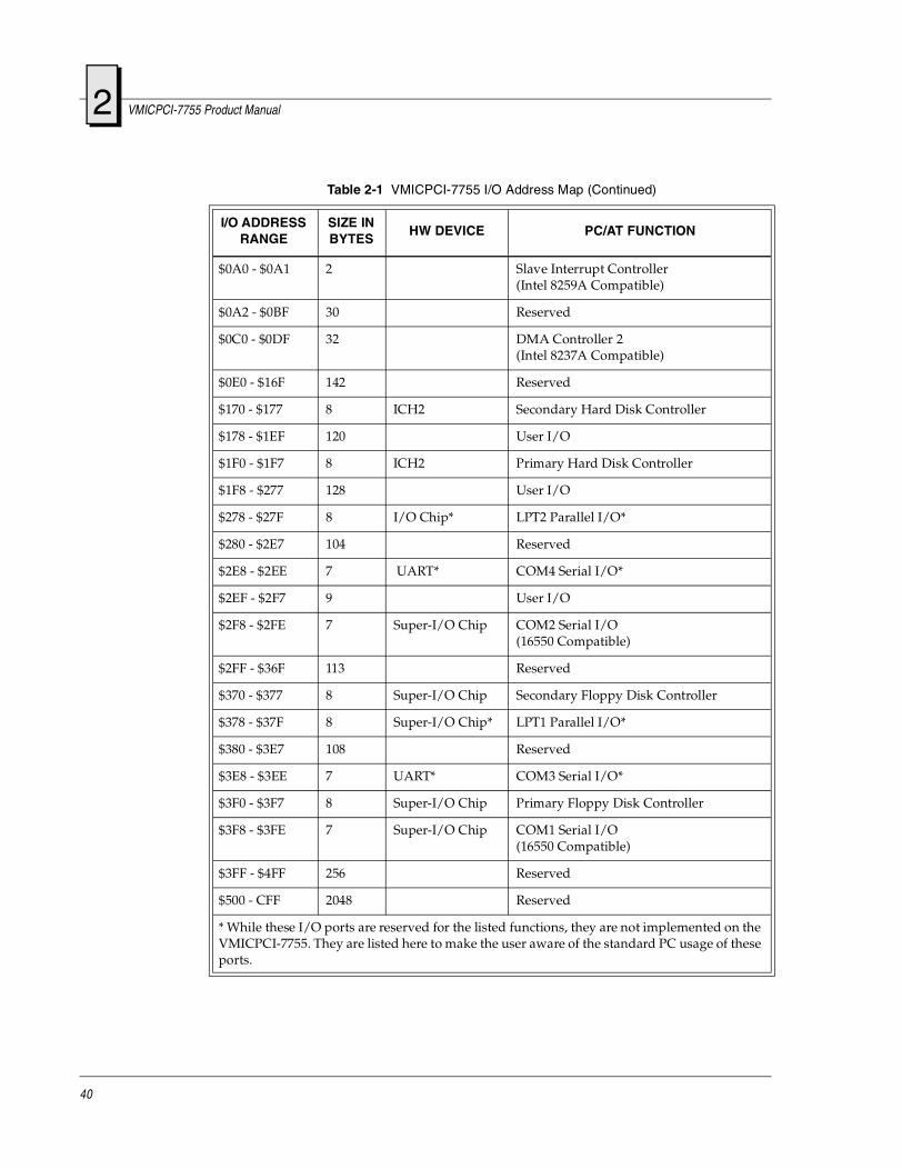
I/O Port Map
Like a desktop system, the VMICPCI-7755 includes special input/output instructions that access I/O peripherals residing in I/O addressing space (separate and distinct from memory addressing space). Locations in I/O address space are referred to as ports. When the CPU decodes and executes an I/O instruction, it produces a 16-bit I/O address on lines A00 to A15 and identifies the I/O cycle with the M/I/O control line. Thus, the CPU includes an independent 64 Kbyte I/O address space, which is accessible as bytes, words or longwords.
Standard hardware circuitry reserves only 1,024 byte of I/O addressing space from I/O $000 to $3FF for peripherals. All standard PC I/O peripherals, such as serial and parallel ports, hard and floppy drive controllers, video system, real-time clock, system timers and interrupt controllers are addressed in this region of I/O space. The BIOS initializes and configures all these registers properly; adjusting these I/O ports directly is not normally necessary.
The assigned and user-available I/O addresses are summarized in the I/O Address Map, Table 2-1.
Table 2-1 VMICPCI-7755 I/O Address Map
I/O ADDRESS RANGE
SIZE INBYTES
HW DEVICE PC/AT FUNCTION
$000 - $00F 16 DMA Controller 1(Intel 8237A Compatible)
$010 - $01F 16 Reserved
$020 - $021 2 Master Interrupt Controller(Intel 8259A Compatible)
$022 - $03F 30 Reserved
$040 - $043 4 Programmable Timer(Intel 8254 Compatible)
$044 - $05F 30 Reserved
$060 - $064 5 Keyboard, Speaker, System Configuration(Intel 8042 Compatible)
$065 - $06F 11 Reserved
$070 - $071 2 Real-Time Clock
$072 - $07F 14 Reserved
$080 - $08F 16 DMA Page Registers
$090 - $091 2 Reserved
$092 1 Alt. Gate A20/Fast Reset Register
$093 - $09F 11 Reserved
39
2 VMICPCI-7755 Product Manual
$0A0 - $0A1 2 Slave Interrupt Controller(Intel 8259A Compatible)
$0A2 - $0BF 30 Reserved
$0C0 - $0DF 32 DMA Controller 2(Intel 8237A Compatible)
$0E0 - $16F 142 Reserved
$170 - $177 8 ICH2 Secondary Hard Disk Controller
$178 - $1EF 120 User I/O
$1F0 - $1F7 8 ICH2 Primary Hard Disk Controller
$1F8 - $277 128 User I/O
$278 - $27F 8 I/O Chip* LPT2 Parallel I/O*
$280 - $2E7 104 Reserved
$2E8 - $2EE 7 UART* COM4 Serial I/O*
$2EF - $2F7 9 User I/O
$2F8 - $2FE 7 Super-I/O Chip COM2 Serial I/O(16550 Compatible)
$2FF - $36F 113 Reserved
$370 - $377 8 Super-I/O Chip Secondary Floppy Disk Controller
$378 - $37F 8 Super-I/O Chip* LPT1 Parallel I/O*
$380 - $3E7 108 Reserved
$3E8 - $3EE 7 UART* COM3 Serial I/O*
$3F0 - $3F7 8 Super-I/O Chip Primary Floppy Disk Controller
$3F8 - $3FE 7 Super-I/O Chip COM1 Serial I/O(16550 Compatible)
$3FF - $4FF 256 Reserved
$500 - CFF 2048 Reserved
* While these I/O ports are reserved for the listed functions, they are not implemented on the VMICPCI-7755. They are listed here to make the user aware of the standard PC usage of these ports.
Table 2-1 VMICPCI-7755 I/O Address Map (Continued)
I/O ADDRESS RANGE
SIZE INBYTES
HW DEVICE PC/AT FUNCTION
40

Interrupts 2
Interrupts
System Interrupts
In addition to an I/O port address, an I/O device has a separate hardware interrupt line assignment. Assigned to each interrupt line is a corresponding interrupt vector in the 256-vector interrupt table at $00000 to $003FF in memory. The 16 maskable interrupts and the single Non-Maskable Interrupt (NMI) are listed in Table 2-2 along with their functions. Table 2-3 on page 42 details the vectors in the interrupt vector table. The interrupt number in HEX and decimal are also defined for real and protected mode in Table 2-3 on page 42.
The interrupt hardware implementation on the VMICPCI-7755 is standard for computers built around the PC architecture, which evolved from the IBM PC/XT. In the IBM PC/XT computers, only eight interrupt request lines exist, numbered from IRQ0 to IRQ7 at the PIC. The IBM PC/AT computer added eight more IRQx lines, numbered IRQ8 to IRQ15, by cascading a second slave PIC into the original master PIC. IRQ2 at the master PIC was committed as the cascade input from the slave PIC. This architecture is represented in Figure 2-1 on page 46.
To maintain backward compatibility with PC/XT systems, IBM chose to use the new IRQ9 input on the slave PIC to operate as the old IRQ2 interrupt line on the PC/XT Expansion Bus. Thus, in AT systems, the IRQ9 interrupt line connects to the old IRQ2 pin (pin B4) on the AT Expansion Bus (or ISA bus).
Table 2-2 PC Hardware Interrupt Line Assignments
IRQ AT FUNCTION COMMENTS
NMI Parity Errors(Must be enabled in BIOS Setup)
Used by VMICPCI-7755 PCIbus Interface
0 System Timer Set by BIOS Setup
1 Keyboard Set by BIOS Setup
2 Duplexed to IRQ9
3 COM2
4 COM1
5 Unused
6 Floppy Controller
7 Unused
8 Real-Time Clock
9 Old IRQ2 SVGA or Network I/O
10 Not Assigned Determined by BIOS
11 Not Assigned Determined by BIOS
41

2 VMICPCI-7755 Product Manual
12 Mouse
13 Math Coprocessor
14 AT Hard Drive
15 Flash Drive
Table 2-3 PC Interrupt Vector Table
INTERRUPT NO.IRQLINE
REAL MODE PROTECTED MODEHEX DEC
00 0 Divide Error Same as Real Mode
01 1 Debug Single Step Same as Real Mode
02 2 NMI Memory Parity Error,CompactPCI Interrupts
Same as Real Mode(Must be enabled in BIOS Setup)
03 3 Debug Breakpoint Same as Real Mode
04 4 ALU Overflow Same as Real Mode
05 5 Print Screen Array Bounds Check
06 6 Invalid OpCode
07 7 Device Not Available
08 8 IRQ0 Timer Tick Double Exception Detected
09 9 IRQ1 Keyboard Input Coprocessor Segment Overrun
0A 10 IRQ2 BIOS Reserved Invalid Task State Segment
0B 11 IRQ3 COM2 Serial I/O Segment Not Present
0C 12 IRQ4 COM1 Serial I/O Stack Segment Overrun
0D 13 IRQ5 Unassigned Unassigned
0E 14 IRQ6 Floppy Disk Controller Page Fault
0F 15 IRQ7 Unassigned Unassigned
10 16 BIOS Video I/O Coprocessor Error
11 17 System Configuration Check Same as Real Mode
12 18 Memory Size Check Same as Real Mode
13 19 XT Floppy/Hard Drive Same as Real Mode
14 20 BIOS Comm I/O Same as Real Mode
15 21 BIOS Cassette Tape I/O Same as Real Mode
Table 2-2 PC Hardware Interrupt Line Assignments (Continued)
IRQ AT FUNCTION COMMENTS
42

Interrupts 2
16 22 BIOS Keyboard I/O Same as Real Mode
17 23 BIOS Printer I/O Same as Real Mode
18 24 ROM BASIC Entry Point Same as Real Mode
19 25 Bootstrap Loader Same as Real Mode
1A 26 Time of Day Same as Real Mode
1B 27 Control/Break Handler Same as Real Mode
1C 28 Timer Control Same as Real Mode
1D 29 Video Parameter Table Pntr Same as Real Mode
1E 30 Floppy Parm Table Pntr Same as Real Mode
1F 31 Video Graphics Table Pntr Same as Real Mode
20 32 DOS Terminate Program Same as Real Mode
21 33 DOS Function Entry Point Same as Real Mode
22 34 DOS Terminate Handler Same as Real Mode
23 35 DOS Control/Break Handler Same as Real Mode
24 36 DOS Critical Error Handler Same as Real Mode
25 37 DOS Absolute Disk Read Same as Real Mode
26 38 DOS Absolute Disk Write Same as Real Mode
27 39 DOS Program Terminate, Stay Resident
Same as Real Mode
28 40 DOS Keyboard Idle Loop Same as Real Mode
29 41 DOS CON Dev. Raw Output Same as Real Mode
2A 42 DOS 3.x+ Network Comm Same as Real Mode
2B 43 DOS Internal Use Same as Real Mode
2C 44 DOS Internal Use Same as Real Mode
2D 45 DOS Internal Use Same as Real Mode
2E 46 DOS Internal Use Same as Real Mode
2F 47 DOS Print Spooler Driver Same as Real Mode
30-60 48-96 Reserved by DOS Same as Real Mode
61-66 97-102 User Available Same as Real Mode
Table 2-3 PC Interrupt Vector Table (Continued)
INTERRUPT NO.IRQLINE
REAL MODE PROTECTED MODEHEX DEC
43

2 VMICPCI-7755 Product Manual
PCI Interrupts
Interrupts on Peripheral Component Interconnect (PCI) Local Bus are optional and defined as “level sensitive,” asserted low (negative true), using open drain output drivers. The assertion and de-assertion of an interrupt line, INTx#, is asynchronous to CLK. A device asserts its INTx# line when requesting attention from its device driver. Once the INTx# signal is asserted, it remains asserted until the device driver clears the pending request. When the request is cleared, the device de-asserts its INTx# signal.
PCI defines one interrupt line for a single function device and up to four interrupt lines for a multifunction device or connector. For a single function device, only INTA# may be used while the other three interrupt lines have no meaning. Figure 2-1 on page 46 depicts the VMICPCI-7755 interrupt logic pertaining to CompactPCI operations and the PMC site.
Any function on a multifunction device can be connected to any of the INTx# lines. The Interrupt Pin register defines which INTx# line the function uses to request an interrupt. If a device implements a single INTx# line, it is called INTA#; if it implements two lines, they are called INTA# and INTB#; and so forth. For a multifunction device, all functions may use the same INTx# line, or each may have its own (up to a maximum of four functions), or any combination thereof. A single function can never generate an interrupt request on more than one INTx# line.
The slave PIC accepts the CompactPCI interrupts through lines that are defined by the BIOS. The BIOS defines which interrupt line to utilize depending on which system requires the use of the line.
67-6F 103-111 Reserved by DOS Same as Real Mode
70 112 IRQ8 Real Time Clock
71 113 IRQ9 Redirect to IRQ2
72 114 IRQ10 Not Assigned
73 115 IRQ11 Not Assigned
74 116 IRQ12 Mouse
75 117 IRQ13 Math Coprocessor
76 118 IRQ14 AT Hard Drive
77 119 IRQ15 Flash Drive
78-7F 120-127 Reserved by DOS Same as Real Mode
80-F0 128-240 Reserved for BASIC Same as Real Mode
F1-FF 241-255 Reserved by DOS Same as Real Mode
Table 2-3 PC Interrupt Vector Table (Continued)
INTERRUPT NO.IRQLINE
REAL MODE PROTECTED MODEHEX DEC
44

Interrupts 2
PCI Device Interrupt Map
The PCI bus-based external devices include the PMC sites, Ethernet controller and the PCI-to-PCI bridge. The default BIOS maps these external devices to the PCI Interrupt Request (PIRQx) lines of the ICH2. This mapping is illustrated in Figure 2-1 on page 46 and is defined in Table 2-4.
The device PCI interrupt lines (INTA through INTD) that are present on each device cannot be modified.
Table 2-4 PCI Device Interrupt Mapping by the BIOS
DEVICE COMPONENT VENDORID
DEVICEID
CPU ADDRESS
MAP ID SELECT
PCI IRQArbitration
Request Line
PCI-to-PCI Bridge Intel 21154 0x1011 0x0026 AD26 N/A REQ0
Timer/SRAM FPGA VMIC Proprietary 0x114A 0x6504 AD20 INTD N/A
PMC1 N/A N/A N/A AD31 INTC REQ3
PMC2 N/A N/A N/A AD30 INTA REQ2
Ethernet Controller Intel 82559ER 0x8086 0x1209 AD22 INTE REQ1
PCI Host Bridge GMCH 0x8086 0x1130 N/A N/A N/A
VGA Controller GMCH 0x8086 0x1132 N/A N/A N/A
PCI-LPC Bridge ICH2 0x8086 0x2440 N/A N/A N/A
VGA Controller ICH2 0x8086 0x2442 N/A N/A N/A
USB Controller #1 ICH2 0x8086 0x2443 N/A N/A N/A
SMBus Controller ICH2 0x8086 0x2444 N/A N/A N/A
USB Controller #2 ICH2 0x8086 0x244B N/A N/A N/A
PCI-to-Hub Bridge ICH2 0x8086 0x244B N/A N/A N/A
45

2 VMICPCI-7755 Product Manual
Figure 2-1 Connections for the PC Interrupt Logic Controller
8259 MASTER- PORTS $020-$021
IRQ0 IRQ1 IRQ2 IRQ4 IRQ5 IRQ7
EMBEDDED
INTA
PCI INTERRUPT
IRQ6IRQ3
CPUINTR
CONNECTIONS
MAPPED BY BIOS
PMC Site #1
BRIDGE
C
PC
bus
Timer Keybd Com 2 Com 1 Unused FloppyControl
Interrupt 8-15
Unused
Real-TmClock
Mouse Math AT FlashHard Drv
NANACoproc
PIRQA PIRQB PIRQC PIRQD
IRQ2
INTB
INTC
INTD
MAPPER
8259 SLAVE- PORTS $0A0-$0A1
I/O Controller HubICH2
INT
Drive
I
BusPCI to PCI
INTA
PMC Site #2
INTB
INTC
INTD
Ethernet
INT
PIRQE
IRQ8 IRQ9 IRQ10 IRQ12IRQ11 IRQ13 IRQ14 IRQ15
FPGA
INT
Timers/SRAM
ompact
46

Interrupts 2
The PCI-to-PCI Bridge has the capability of generating a Non-Maskable Interrupt (NMI) via the PCI SERR# line. Table 2-5 describes the register bits that are used by the NMI. The SERR interrupt is routed through logic back to the NMI input line on the CPU. The CPU reads the NMI Status Control register to determine the NMI source (bits set to 1). After the NMI interrupt routine processes the interrupt, software clears the NMI status bits by setting the corresponding enable/disable bit to 1. The NMI Enable and Real-Time Clock register can mask the NMI signal and disable/enable all NMI sources.
Table 2-5 NMI Register Bit Descriptions
Status Control Register (I/O Address $061, Read/Write, Read Only)
Bit 7SERR# NMI Source Status (Read Only) - This bit is set to 1 if a system board agent detects a system board error. It then asserts the PCI SERR# line. To reset the interrupt, set Bit 2 to 0 and then set it to 1. When writing to port $061, Bit 7 must be 0.
Bit 2 PCI SERR# Enable (Read/Write) - 1 = Clear and Disable, 0 = Enable
Enable and Real-Time Clock Address Register (I/O Address $070, Write Only)
Bit 7 NMI Enable - 1 = Disable, 0 = Enable
47

2 VMICPCI-7755 Product Manual
Integrated Peripherals
The VMICPCI-7755 incorporates a National Semiconductor Super I/O (SIO) chip. The SIO provides the VMICPCI-7755 with a standard floppy drive controller, two 16550 UART-compatible serial ports keyboard and mouse ports, and general purpose I/O for system monitoring functions. The floppy and serial port signals are available via the CompactPCI backplane connectors and can be accessed with the appropriate transition utility board.
The IDE interface is provided by the Intel I/O Controller Hub (ICH2) chip. The IDE interface supports two channels known as the primary and secondary channels. The secondary channel is routed on-board to the optional compact flash socket. The primary channel is routed out the CompactPCI backplane to a transition utility board which terminates into a standard 40-pin header. This channel can support two drives, a master and slave. The IDE interface on the VMICPCI-7755 supports ATA-33, ATA-66, and ATA-100 drives and automatically determines the proper operating mode based on the type of drive used. In order to properly function in the ATA-100 mode, a special 80 conductor cable must be used instead of the standard 40 conductor cable. This cable is typically available from the ATA-100 drive manufacturer.
48

Ethernet Controller 2
Ethernet Controller
The network capability is provided by the Intel 82559ER Ethernet Controller. This Ethernet controller is PCI bus based and is software configurable. The VMICPCI-7755 supports 10BaseT and 100BaseTx Ethernet.
10BaseT
A network based on the 10BaseT standard uses unshielded twisted-pair cables, providing an economical solution to networking by allowing the use of existing telephone wiring and connectors. The RJ-45 connector is used with the 10BaseT standard. 10BaseT has a maximum length of 100 meters.
100BaseTx
The VMICPCI-7755 also supports the 100BaseTx Ethernet. A network based on a 100BaseTx standard uses unshielded twisted-pair cables and a RJ-45 connector. The 100BaseTx has a maximum length of 100 meters.
49

2 VMICPCI-7755 Product Manual
Video Graphics Adapter
The SVGA port on the VMICPCI-7755 is controlled by the Intel Graphic and Memory Controller Hub (GMCH) chip with 4 Mbyte video DRAM. The GMCH is hardware and BIOS compatible with the industry EGA and SVGA standards supporting both VESA high-resolution and extended video modes. Table 2-6 shows the graphics video modes supported by the GMCH video controller.
Not all SVGA monitors support resolutions and refresh rates beyond 640 x 480 at 85 Hz. Do not attempt to drive a monitor to a resolution or refresh rate beyond its capability.
Table 2-6 Supported Graphics Video Resolutions
Screen Resolution
Maximum Colors
Maximum Refresh Rates (Hz)
640 x 480 16 M 85
800 x 600 16 M 85
1024 x 768 16 M 85
1280 x 1024 16 M 85
1600 x 900 64 K 85
1600 x 1200 256 75
50

CHAPTER
3
Embedded PC/RTOS Features
Contents
CompactPCI Bus Bridge . . . . . . . . . . . . . . . . . . . . . . . . . . . . . . . . . . . . . . . . . . . . . . 52I2C Support . . . . . . . . . . . . . . . . . . . . . . . . . . . . . . . . . . . . . . . . . . . . . . . . . . . . . . . . . 53
Embedded PCI Functions . . . . . . . . . . . . . . . . . . . . . . . . . . . . . . . . . . . . . . . . . . . . . 54Timers . . . . . . . . . . . . . . . . . . . . . . . . . . . . . . . . . . . . . . . . . . . . . . . . . . . . . . . . . . . . . 55
Watchdog Timer . . . . . . . . . . . . . . . . . . . . . . . . . . . . . . . . . . . . . . . . . . . . . . . . . . . . . 61NVSRAM. . . . . . . . . . . . . . . . . . . . . . . . . . . . . . . . . . . . . . . . . . . . . . . . . . . . . . . . . . . 63
Flash Disk . . . . . . . . . . . . . . . . . . . . . . . . . . . . . . . . . . . . . . . . . . . . . . . . . . . . . . . . . . 64Remote Ethernet Booting . . . . . . . . . . . . . . . . . . . . . . . . . . . . . . . . . . . . . . . . . . . . . 67
Introduction
VMIC’s VMICPCI-7755 features additional capabilities beyond those of a typical desktop computer system. The unit provides four software-controlled, general-purpose timers along with a programmable Watchdog Timer for synchronizing and controlling multiple events in embedded applications. The VMICPCI-7755 also provides a bootable Flash Disk system and 32 Kbyte of non-volatile SRAM. Also, the VMICPCI-7755 supports an embedded intelligent CompactPCI bridge to allow compatibility with the most demanding CompactPCI applications. These features make the unit ideal for embedded applications, particularly where standard hard drives and floppy disk drives cannot be used. The VMICPCI-7755 also supports I2C by integrating specialized circuitry for these functions.
51

3 VMICPCI-7755 Product Manual
CompactPCI Bus Bridge
The VMICPCI-7755 incorporates a PCI peripheral device that performs PCI bridging functions for embedded and intelligent I/O applications. The PCI device acts as a gateway to an intelligent subsystem. It allows the local VMICPCI-7755 processor to configure and control the on-board local subsystem independent from the CompactPCI bus host processor. The VMICPCI-7755 local PCI subsystem is presented to the CompactPCI bus host as a single CompactPCI device. For detailed information concerning the embedded PCI bus bridge, consult the DEC/Intel datasheet “21154 PCI-to-PCI Bridge for Embedded Applications”.
The VMICPCI-7755 PCI bridge device provides the following features:
PCI Interface
• Full compliance with the PCI Local Bus Specification, Revision 2.1• 3.3 V operation with 5.0 V tolerant I/O• Concurrent local (secondary) and CompactPCI (primary) bus operation
Buffer Architecture
• Queuing of multiple transactions in either direction• 256 byte of posted write (data and address) buffering in each direction• 256 byte of read data buffering in each direction• Four delayed transaction entries in each direction
Configuration Register and Control/Status Registers (CSRs)
• Two sets of standard PCI configuration registers corresponding to the local and CompactPCI interfaces: accessible from either the local or CompactPCI interface
• Four 32-bit base address configuration registers mapping the CSRs
Transaction Forwarding
• Four primary interface base address configuration registers for downstream forwarding with size and prefetchable programming for all four address ranges
• Direct offset address translation for downstream memory and I/O transactions• Three secondary interface address ranges for upstream forwarding, with size
and prefetchable programming for all three address ranges• Inverse decoding above 4 Gbyte address boundary for upstream
Digital-to-Analog Controllers (DACs)• Ability to generate type 0 and type 1 configuration commands on the primary
or secondary interface by way of configuration cycles or I/O cycles accessing the CSR
52

I2C Support 3
I2C Support
The VMICPCI-7755 supports the I2C-bus and can operate as an I2C-bus master or slave per the I2C-bus specification, version 2.0, developed by Philips Semiconductor. Communication over the I2C-bus is accomplished through the use of the National Semiconductor Super I/O I2C-bus controller. This controller is capable of communicating on the I2C-bus on a byte-wise basis using interrupt or polled handshaking and supports a programmable clock rate when operating in Master mode. The I2C-bus signals are routed through the VMICPCI-7755’s J1 connector as shown in Table 3-1.
Because multiple processors may share the I2C signals, the VMICPCI-7755 does not provide pull-ups on the I2C signals. This gives the system the flexibility of setting the pull-up voltage level of the I2C bus with a single pair of pull-up resisters located on the system controller, backplane or any other connected system device.
The controller can issue interrupts to the VMICPCI-7755 when handshaking on the I2C-bus. When the I2C-bus controller drives the interrupt active, software must service and then clear the interrupt. Software can determine the cause of the interrupt by reading the bit of the status register.
For more information related to programming the I2C-bus controller, see the section “Access, Bus Interface (ACB)” in the “PC87366 128-pin LPC Super I/O with System Hardware Monitoring and MIDI and Game Ports” datasheet available from National Semiconductor.
Table 3-1 I2C-bus Through J1
Signal Name Pin
I2C_SCL B17
I2C_SDA C17
The user must supply appropriate pullups on these pins.
53

3 VMICPCI-7755 Product Manual
Embedded PCI Functions
The VMICPCI-7755 provides non-volatile RAM (NVRAM), Timers and a Watchdog Timer via the PCI bus. These functions are required for embedded and real time applications. The PCI configuration space of these embedded functions are shown below.
The “Device ID” field indicates that the device is for CompactPCI products (65) and indicates the supported embedded feature set.
The “Vender ID” and “Subsystem Vendor ID” fields indicate VMIC’s PICMG assigned Vender ID (114A).
The “Subsystem ID” field indicates the model number of the product (7755).
Table 3-2 PCI Configuration Space Registers
31 16 15 00 RegisterAddress
Device ID 6504 Vendor ID 114A 00h
Status Command 04h
Class Code Revision ID 08h
BIST Header Type Latency Timer Cache Line Size 0Ch
PCI Base Address 0 for Memory-Mapped 32kb NVRAM 10h
PCI Base Address 1 for Memory-Mapped Watchdog and other Timers 14h
Reserved 18h
Reserved 1Ch
Reserved 20h
Reserved 24h
Reserved 28h
Subsystem ID 7755 Subsystem Vendor ID 114A 2Ch
Reserved 30h
Reserved 34h
Reserved 38h
Max_Lat Min_gnt Interrupt Pin Interrupt Line 3Ch
54

Timers 3
Timers
General
The VMICPCI-7755 provides four user-programmable timers (two 16-bit and two 32-bit) which are dedicated completely to user applications and are not required for any standard system function. Each timer is clocked by independent generators with selectable rates of 2MHz, 1MHz, 500kHz and 250kHz. Each timer may be independently enabled and each is capable of generating a system interrupt on timeout.
Events can be timed by either polling the timers or enabling the interrupt capability of the timer. A status register allows for application software to determine which timer is the cause of any interrupt.
Timer Control Status Register 1 (TCSR1)
The timers are controlled and monitored via the Timer Control Status Register 1 (TCSR1) located at offset 0x00 from the address in BAR1. The mapping of the bits in this register are as follows:
Field Bits Read or Write
Timer 1 Caused IRQ TCSR1[0] R/W
Timer 1 Enable TCSR1[1] R/W
Timer 1 IRQ Enable TCSR1[2] R/W
Timer 1 Clock Select TCSR1[4..3] R/W
Timer 2 Caused IRQ TCSR1[8] R/W
Timer 2 Enable TCSR1[9] R/W
Timer 2 IRQ Enable TCSR1[10] R/W
Timer 2 Clock Select TCSR1[12..11] R/W
Timer 3 Caused IRQ TCSR1[16] R/W
Timer 3 Enable TCSR1[17] R/W
Timer 3 IRQ Enable TCSR1[18] R/W
Timer 3 Clock Select TCSR1[20..19] R/W
Timer 4 Caused IRQ TCSR1[24] R/W
Timer 4 Enable TCSR1[25] R/W
Timer 4 IRQ Enable TCSR1[26] R/W
Timer 4 Clock Select TCSR1[28..27] R/W
Reserved All Other Bits R/W
All of these bits default to “0” after system reset.
55
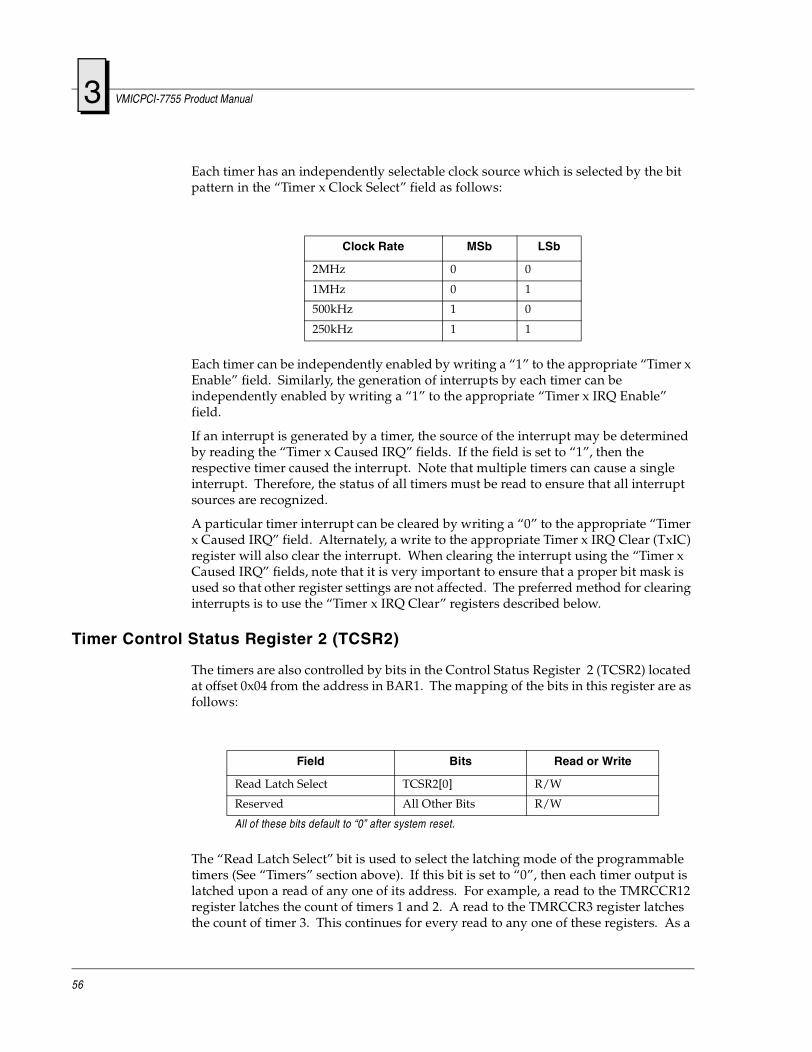
3 VMICPCI-7755 Product Manual
Each timer has an independently selectable clock source which is selected by the bit pattern in the “Timer x Clock Select” field as follows:
Each timer can be independently enabled by writing a “1” to the appropriate “Timer x Enable” field. Similarly, the generation of interrupts by each timer can be independently enabled by writing a “1” to the appropriate “Timer x IRQ Enable” field.
If an interrupt is generated by a timer, the source of the interrupt may be determined by reading the “Timer x Caused IRQ” fields. If the field is set to “1”, then the respective timer caused the interrupt. Note that multiple timers can cause a single interrupt. Therefore, the status of all timers must be read to ensure that all interrupt sources are recognized.
A particular timer interrupt can be cleared by writing a “0” to the appropriate “Timer x Caused IRQ” field. Alternately, a write to the appropriate Timer x IRQ Clear (TxIC) register will also clear the interrupt. When clearing the interrupt using the “Timer x Caused IRQ” fields, note that it is very important to ensure that a proper bit mask is used so that other register settings are not affected. The preferred method for clearing interrupts is to use the “Timer x IRQ Clear” registers described below.
Timer Control Status Register 2 (TCSR2)
The timers are also controlled by bits in the Control Status Register 2 (TCSR2) located at offset 0x04 from the address in BAR1. The mapping of the bits in this register are as follows:
The “Read Latch Select” bit is used to select the latching mode of the programmable timers (See “Timers” section above). If this bit is set to “0”, then each timer output is latched upon a read of any one of its address. For example, a read to the TMRCCR12 register latches the count of timers 1 and 2. A read to the TMRCCR3 register latches the count of timer 3. This continues for every read to any one of these registers. As a
Clock Rate MSb LSb
2MHz 0 0
1MHz 0 1
500kHz 1 0
250kHz 1 1
Field Bits Read or Write
Read Latch Select TCSR2[0] R/W
Reserved All Other Bits R/W
All of these bits default to “0” after system reset.
56

Timers 3
result, it is not possible to capture the values of all four timers at a give instance in time. However, by setting this bit to “1”, all four timer outputs will be latched only on reads to the Timer 1 & 2 Current Count Register (TMRCCR12). Therefore, to capture the current count of all four timers at the same time, perform a read to the TMRCCR12 first (with a 32-bit read), followed by a read to TMRCCR3 and TMRCCR4. The first read (to the TMRCCR12 register) causes all four timer values to be latched at the same time. The subsequent reads to the TMRCCR3 and TMRCCR4 registers do not latch new count values, allowing the count of all timers at the same instance in time to be obtained.
Timer 1 & 2 Load Count Register (TMRLCR12)
Timers 1 & 2 are 16-bits wide and obtain their load count from the Timer 1 & 2 Load Count Register (TMRLCR12), located at offset 0x10 from the address in BAR1. The mapping of bits in this register are as follows:
When either of these fields are written (either by a single 32-bit write or separate 16-bit writes), the respective timer is loaded with the written value on the next rising edge of the timer clock, regardless of whether the timer is enabled or disabled. The value stored in this register is also automatically reloaded on terminal count (or timeout) of the timer.
Timer 3 Load Count Register (TMRLCR3)
Timer 3 is 32-bits wide and obtains its load count from the Timer 3 Load Count Register (TMRLCR3), located at offset 0x14 from the address in BAR1. The mapping of bits in this register are as follows:
When this field is written, Timer 3 is loaded with the written value on the next rising edge of the timer clock, regardless of whether the timer is enabled or disabled. The value stored in this register is also automatically reloaded on terminal count (or timeout) of the timer.
Field Bits Read or Write
Timer 2 Load Count TMRLCR12[31..16] R/W
Timer 1 Load Count TMRLCR12[15..0] R/W
Field Bits Read or Write
Timer 3 Load Count TMRLCR3[31..0] R/W
57

3 VMICPCI-7755 Product Manual
Timer 4 Load Count Register (TMRLCR4)
Timer 4 is 32-bits wide and obtains its load count from the Timer 4 Load Count Register (TMRLCR4), located at offset 0x18 from the address in BAR1. The mapping of bits in this register are as follows:
When this field is written, Timer 4 is loaded with the written value on the next rising edge of the timer clock, regardless of whether the timer is enabled or disabled. The value stored in this register is also automatically reloaded on terminal count (or timeout) of the timer.
Timer 1 & 2 Current Count Register (TMRCCR12)
The current count of timers 1 & 2 may be read via the Timer 1 & 2 Current Count Register (TMRCCR12), located at offset 0x20 from the address in BAR1. The mapping of bits in this register are as follows:
When either field is read, the current count value is latched and returned. There are two modes that determine how the count is latched depending on the setting of the “Read Latch Select” bit in the WDT Control Status Register (CSR2). See the CSR2 register description for more information on these two modes.
Timer 3 Current Count Register (TMRCCR3)
The current count of Timer 3 may be read via the Timer 3 Current Count Register (TMRCCR3), located at offset 0x24 from the address in BAR1. The mapping of bits in this register are as follows:
Field Bits Read or Write
Timer 4 Load Count TMRLCR4[31..0] R/W
Field Bits Read or Write
Timer 2 Count TMRCCR12[31..16] R.O.
Timer 1 Count TMRCCR12[15..0] R.O.
Field Bits Read or Write
Timer 3 Count TMRCCR3[31..0] R.O.
58

Timers 3
When this field is read, the current count value is latched and returned. There are two modes that determine how the count is latched depending on the setting of the “Read Latch Select” bit in the WDT Control Status Register (CSR2). See the CSR2 register description for more information on these two modes.
Timer 4 Current Count Register (TMRCCR4)
The current count of Timer 3 may be read via the Timer 4 Current Count Register (TMRCCR4), located at offset 0x28 from the address in BAR1. The mapping of bits in this register are as follows:
When this field is read, the current count value is latched and returned. There are two modes that determine how the count is latched depending on the setting of the “Read Latch Select” bit in the WDT Control Status Register (CSR2). See the CSR2 register description for more information on these two modes.
Timer 1 IRQ Clear (T1IC)
The Timer 1 IRQ Clear (T1IC) register is used to clear an interrupt caused by Timer 1. Writing to this register, located at offset 0x30 from the address in BAR1, causes the interrupt from Timer 1 to be cleared. This can also be done by writing a “0” to the appropriate “Timer x Caused IRQ” field of the timer Control Status Register (CSR1). This register is write only and the data written is irrelevant.
Timer 2 IRQ Clear (T12C)
The Timer 2 IRQ Clear (T2IC) register is used to clear an interrupt caused by Timer 2. Writing to this register, located at offset 0x34 from the address in BAR1, causes the interrupt from Timer 2 to be cleared. This can also be done by writing a “0” to the appropriate “Timer x Caused IRQ” field of the timer Control Status Register (CSR1). This register is write only and the data written is irrelevant.
Timer 3 IRQ Clear (T3IC)
The Timer 3 IRQ Clear (T3IC) register is used to clear an interrupt caused by Timer 3. Writing to this register, located at offset 0x38 from the address in BAR1, causes the interrupt from Timer 3 to be cleared. This can also be done by writing a “0” to the appropriate “Timer x Caused IRQ” field of the timer Control Status Register (CSR1). This register is write only and the data written is irrelevant.
Field Bits Read or Write
Timer 4 Count TMRCCR4[31..0] R.O.
59

3 VMICPCI-7755 Product Manual
Timer 4 IRQ Clear (T4IC)
The Timer 4 IRQ Clear (T4IC) register is used to clear an interrupt caused by Timer 4. Writing to this register, located at offset 0x3C from the address in BAR1, causes the interrupt from Timer 4 to be cleared. This can also be done by writing a “0” to the appropriate “Timer x Caused IRQ” field of the timer Control Status Register (CSR1). This register is write only and the data written is irrelevant.
60

Watchdog Timer 3
Watchdog Timer
General
The VMICPCI-7755 provides a programmable Watchdog Timer (WDT) which can be used to reset the system if software integrity fails.
WDT Control Status Register (WCSR)
The WDT is controlled and monitored by the WDT Control Status Register (WCSR) which is located at offset 0x08 from the address in BAR1. The mapping of the bits in this register are as follows:
The “WDT Timeout Select” field is used to select the timeout value of the Watchdog Timer as follows:
The “SERR/RST Select” bit is used to select whether the WDT generates an SERR# on the local PCI bus or a system reset. If this bit is set to “0”, the WDT will generate a system reset. Otherwise, the WDT will make the local PCI bus SERR# signal active.
Field Bits Read or Write
SERR/RST Select WCSR[16] R/W
WDT Timeout Select WCSR[10..8] R/W
WDT Enable WCSR[0] R/W
All of these bits default to “0” after system reset. All other bits are reserved.
Timeout WCSR[10] WCSR[9] WCSR[8]
135s 0 0 0
33.6s 0 0 1
2.1s 0 1 0
524ms 0 1 1
262ms 1 0 0
131ms 1 0 1
32.768ms 1 1 0
2.048ms 1 1 1
61
3 VMICPCI-7755 Product Manual
The “WDT Enable” bit is used to enable the Watchdog Timer function. This bit must be set to “1” in order for the Watchdog Timer to function. Note that since all registers default to zero after reset, the Watchdog Timer is always disabled after a reset. The Watchdog Timer must be re-enabled by the application software after reset in order for the Watchdog Timer to continue to operate. Once the Watchdog Timer is enabled, the application software must refresh the Watchdog Timer within the selected timeout period to prevent a reset or SERR# from being generated. The Watchdog Timer is refreshed by performing a write to the WDT Keepalive register (WKPA). The data written is irrelevant.
WDT Keepalive Register (WKPA)
When enabled, the Watchdog Timer is prevented from resetting the system by writing to the WDT Keepalive Register (WKPA) located at offset 0x0C from the address in BAR1 within the selected timeout period. The data written to this location is irrelevant.
62

NVSRAM 3
NVSRAM
The VMICPCI-7755 provides 32KBytes of non-volatile SRAM. This memory is mapped in 32K of address space starting at the address in BAR0. This memory is available at any time and supports byte, short word and long word accesses from the PCI bus. The contents of this memory is retained when the power to the board is removed.
63

3 VMICPCI-7755 Product Manual
Flash Disk
The VMICPCI-7755 features an optional on-board Compact Flash mass storage system with a capacity of up to 192 Mbyte. This Flash Disk appears to the user as an intelligent ATA (IDE) disk drive with the same functionality and capabilities as a “rotating media” IDE hard drive. The VMICPCI-7755 BIOS includes an option to allow the board to boot from the Flash Disk.
Configuration
The Flash Disk resides on the VMICPCI-7755 as the secondary IDE bus master device (the secondary IDE bus slave device is not assignable). The default setting in the Phoenix BIOS ‘STANDARD CMOS SETUP’ screen is the ‘AUTO’ setting. In the Phoenix BIOS ‘PERIPHERAL SETUP’ screen, the secondary PCI IDE interface must be enabled for the Flash Disk to be functional. Refer to Appendix C for additional details.
Figure 3-1 maps the configuration possibilities for a typical system consisting of the VMICPCI-7755 with a resident Flash Disk, a hard drive attached to the Primary IDE interface, and a floppy drive attached to the floppy interface.
Figure 3-1 Typical System Configuration
The Primary and Secondary PCI IDE Interfaces are controlled (enabled or disabled) in the Integrated Peripheral Setup screen of the Phoenix BIOS. The First Boot Device is selected in the BIOS Features Setup screen.
Figure 3-1 identifies the drive letter assigned to each physical device, and indicates in bold lettering the device booted from in each configuration, using devices that are bootable. A bootable device is one on which an operating system has been installed, or formatted as a system disk using MS-DOS.
Hard Drive C: C: D: C: C: C: N/A N/A N/A
Flash Disk D: D: C: N/A N/A N/A C: C: C:
Floppy Drive A: A: A: A: A: A: A: A: A:
Primary and Secondary
Primary Only Secondary Only
A: C; SCSIC: A; SCSIFlash Disk{Selected
“Boot Sequence”
PCI IDE Interface Enabled
64

Flash Disk 3
Functionality
The Flash Disk performs identically to a standard IDE hard drive. Reads and writes to the device are performed using the same methods, utilizing DOS command line entries or the file managers resident in the chosen operating system.
Advanced Configuration
The previous discussion is based on using the IDE disk devices formatted as one large partition per device. Some applications may require the use of multiple partitions. The following discussion of these partitions includes special procedures that must be followed to create multiple partitions on the VMICPCI-7755 IDE disk devices (including the resident Flash Disk).
Partitions may be either a primary or an extended partition. An extended partition may be subdivided farther into logical partitions. Each device may have up to four main partitions; one of which may be an extended partition. However, if multiple primary partitions are created, only one partition may be active at a time. Data in the non-active partitions are not accessible.
Following the creation of the partitioning scheme, the partitions can be formatted to contain the desired file system.
As discussed earlier, a typical system consists of the VMICPCI-7755 with its resident Flash Disk configured as the Secondary IDE device, a hard drive attached to the Primary IDE interface, and a floppy drive attached to the floppy interface.
Using this configuration, it may be desirable to have a logical device on either IDE device, configured as a bootable device, allowing the selection of the first boot device by way of the Advanced CMOS Setup screen. Using this capability, a user could have a system configured with multiple operating systems that would be selectable by assigning the IDE logical device as the boot device.
The DOS utility FDISK is commonly used to configure the partition structure on a hard drive. Comments on the following page pertain to partitioning efforts using FDISK.
CAUTION: Deleting a partition will erase all the data previously stored in that partition.
The Flash Disk will be configured as a single partition device as delivered from the factory. The following sample sequence illustrates a proven method for creating two 8 Mbyte partitions, with one as an active primary partition. Take note of the instructions to exit FDISK. This has been shown to be an important step in a successful partitioning effort.
1. Power up the VMICPCI-7755 and enter the CMOS set-up.
2. Set IDE HDD Master to “Not Installed”.
65

3 VMICPCI-7755 Product Manual
3. Set Flash Disk Master to “AUTO”.
4. Set boot device to floppy.
5. Boot DOS from the floppy, and verify that the System Configuration Screen shows only the Flash Disk.
6. Run FDISK.
7. Delete all current partitions (any data currently stored in the partitions will be lost).
8. Exit FDISK (this will cause a reboot), then run FDISK again.
9. Create an 8 Mbyte primary partition.
10. Create an 8 Mbyte extended partition.
11. Set-up a logical device for the 8 Mbyte extended partition.
12. Set the Primary partition as an active partition.
13. Exit FDISK.
If an operating system has been installed on the Flash Disk that modifies the Master Boot Record (MBR), the following steps are required to rewrite the MBR for DOS.
14. Run FDISK/MBR.
15. Run FORMAT C: (use the extension /s option if you want the Flash Disk as a bootable DOS device).
16. Format D: (this is only required if two partitions were created).
17. Reset the CPU and enter the CMOS set-up.
18. Set Primary Master to “AUTO”.
19. Set boot device to desired boot source.
Drive letter assignments for a simple system are illustrated in Figure 3-1 on page 64. Understanding the order the operating system assigns drive letters is necessary for these multiple partition configurations. The operating system assigns drive letter C to the active primary partition on the first hard disk (the boot device). Drive D is assigned to the first recognized primary partition on the next hard disk. The operating system will continue to assign drive letters to the primary partitions in an alternating fashion between the two drives. The next logical partitions will be assigned drive letters starting on the first hard drive, lettering each logical device sequentially, until all are assigned a drive letter. The system will then perform the same sequential lettering of each logical partition on the second hard disk.
NOTE: Drive letter changes caused by adding an additional drive or changing the initial partitioning scheme may cause difficulties with an operating system installed prior to the changes. Plan your configuration prior to installing the operating system to minimize difficulties.
66

Remote Ethernet Booting 3
Remote Ethernet Booting
The VMICPCI-7755 is capable of booting from a server over a network utilizing Lanworks BootWare BIOS. The BootWare BIOS gives you the ability to remotely boot the VMICPCI-7755 using a variety of network protocols. The Ethernet must be connected through the LAN front panel (RJ-45) connector to boot remotely. This feature allows users to create systems without the worry of disk drive reliability, or the extra cost of adding Flash drives.
BootWare Features:
• Netware (802.1, 802.3 or EthII), TCP/IP (DHCP or BootP), RPL and PXE boot support
• Unparalleled boot sector virus protection• Detailed boot configuration screens
• Comprehensive diagnostics• Optional disabling of local boots
• Dual-boot option lets users select network or local booting
67

3 VMICPCI-7755 Product Manual
68

CHAPTER
4
Maintenance
If a VMIC product malfunctions, please verify the following:
1. Software resident on the product
2. System configuration
3. Electrical connections
4. Jumper or configuration options
5. Boards are fully inserted into their proper connector location
6. Connector pins are clean and free from contamination
7. No components or adjacent boards were disturbed when inserting or removing the board from the chassis
8. Quality of cables and I/O connections
If products must be returned, contact VMIC for a Return Material Authorization (RMA) Number. This RMA Number must be obtained prior to any return.
VMIC Customer Service is available at: 1-800-240-7782.Or E-mail us at [email protected]
Maintenance Prints
User level repairs are not recommended. The drawings and diagrams in this manual are for reference purposes only.
69

4 VMICPCI-7755 Product Manual
70

Appendix
A
Connector Pinouts
Contents
J1 Connector Pinout. . . . . . . . . . . . . . . . . . . . . . . . . . . . . . . . . . . . . . . . . . . . . . . . . . 72J2 Connector Pinout. . . . . . . . . . . . . . . . . . . . . . . . . . . . . . . . . . . . . . . . . . . . . . . . . . 73
J3 Connector Pinout. . . . . . . . . . . . . . . . . . . . . . . . . . . . . . . . . . . . . . . . . . . . . . . . . . 74J4 Connector Pinout (Optional) . . . . . . . . . . . . . . . . . . . . . . . . . . . . . . . . . . . . . . . . 75
J5 Connector Pinout. . . . . . . . . . . . . . . . . . . . . . . . . . . . . . . . . . . . . . . . . . . . . . . . . . 76Ethernet Connector Pinout (J6) . . . . . . . . . . . . . . . . . . . . . . . . . . . . . . . . . . . . . . . . 77
Video Connector Pinout (P3) . . . . . . . . . . . . . . . . . . . . . . . . . . . . . . . . . . . . . . . . . . 78Keyboard and Mouse Connectors and Pinout (J7) . . . . . . . . . . . . . . . . . . . . . . . . 79
PMC Connector Pinout . . . . . . . . . . . . . . . . . . . . . . . . . . . . . . . . . . . . . . . . . . . . . . . 80
Introduction
The VMICPCI-7755 CompactPCI Peripheral SBC has several connectors for its I/O ports. Wherever possible, the VMICPCI-7755 uses connectors and pinouts typical for any desktop PC. This ensures maximum compatibility with a variety of systems.
Connector diagrams in this appendix are generally shown in a natural orientation with the controller board mounted in a CompactPCI bus chassis.
71

A VMICPCI-7755 Product Manual
J1 Connector Pinout
The VMICPCI-7755 utilitizes a high-density 110-pin, low inductance, and controlled impedance connector. This connector meets the IEC-1076 international standard for CompactPCI connectors. An additional external metal shield is required. The large number of ground pins ensures adequate shielding and grounding for low ground bounce and reliable operation in noisy environments. The key prevents misalignment of the board when installing in the chassis. Figure A-1 below depicts the J1 connector and the connector pinout.
Figure A-1 J1 Connector and Pinout
Pin No. Row A Row B Row C Row D Row E Row F
25 +5 V C_REQ64# C_ENUM# CPCI_3.3 +5 V GND
24 C_AD[1] +5 V CPCI_VIO C_AD[0] C_ACK64# N/C
23 CPCI_3.3 C_AD[4] C_AD[3] +5 V C_AD[2] GND
22 C_AD[7] GND CPCI_3.3 C_AD[6] C_AD[5] N/C
21 CPCI_3.3 C_AD[9] C_AD[8] GND C_C/BE0# GND
20 C_AD[12] GND CPCI_VIO C_AD[11] C_AD[10] N/C
19 CPCI_3.3 C_AD[15] C_AD[14] GND C_AD[13] GND
18 C_SERR# GND CPCI_3.3 C_PAR C_C/BE1# N/C
17 CPCI_3.3 I2C_SCL I2C_SDA GND C_PERR# GND
16 C_DEVSEL# GND CPCI_VIO C_STOP# C_LOCK# N/C
15 CPCI_3.3 C_FRAME C_IRDY# N/C C_TRDY# GND
12 through 14 are lost to the keying area
11 C_AD[18] C_AD[17] C_AD[16] GND C_C/BE2# GND
10 C_AD[21] GND CPCI_3.3 C_AD[20] C_AD[19] N/C
9 C_CBE3# N/C C_AD[23] GND C_AD[22] GND
8 C_AD[26] GND CPCI_VIO C_AD[25] C_AD[24] N/C
7 C_AD[30] C_AD[29] C_AD[28] GND C_AD[27] GND
6 C_REQ# GND CPCI_3.3 C_CLK C_AD[31] N/C
5 N/C N/C C_RST# GND C_GNT# GND
4 N/C N/C CPCI_VIO N/C N/C N/C
3 C_INTA# C_INTB# C_INTC# +5 V C_INTD# GND
2 C_TCK +5 V C_TMS N/C C_TDI N/C
1 +5 V -12 V C_TRST# +12 V +5 V GND
72

J2 Connector Pinout A
J2 Connector Pinout
The VMICPCI-7755 J2 connector is a 2mm “Hard Metric” CompactPCI connector, with 5 rows of 22 pins each. J2 is required for system slot CPUs. An additional external metal shield, labeled row F, is also used. This connector’s controlled impedance minimizes unwanted signal reflections. Figure A-2 illustrates the J2 connector and the connector pinout.
Figure A-2 J2 Connector and Pinout
Pin No. Row A Row B Row C Row D Row E Row F
22 N/C N/C N/C N/C N/C GND
21 C_CLK6 GND N/C N/C N/C N/C
20 C_CLK5 GND N/C GND N/C GND
19 GND GND N/C N/C N/C N/C
18 N/C N/C N/C GND N/C GND
17 N/C GND C_PRST# C_REQ6# C_GNT6# N/C
16 N/C N/C PULLUP GND N/C GND
15 N/C GND PULLUP C_REQ5# C_GNT5# N/C
14 C_AD35 C_AD34 C_AD33 GND C_AD32 GND
13 C_AD38 GND CPCI_VIO C_AD37 C_AD36 N/C
12 C_AD42 C_AD41 C_AD40 GND C_AD39 GND
11 C_AD45 GND CPCI_VIO C_AD44 C_AD43 N/C
10 C_AD49 C_AD48 C_AD47 GND C_AD46 GND
9 C_AD52 GND CPCI_VIO C_AD57 C_AD50 N/C
8 C_AD56 C_AD55 C_AD54 GND C_AD53 GND
7 C_AD59 GND CPCI_VIO C_AD58 C_AD57 N/C
6 C_AD63 C_AD62 C_AD61 GND C_AD60 GND
5 C_BE5# C_64E# CPCI_VIO C_BE4# C_PAR64 N/C
4 CPCI_VIO N/C C_BE7# GND C_BE6# GND
3 C_CLK4 GND C_GNT3# C_REQ4# C_GNT4# N/C
2 C_CLK2 C_CLK3 GND C_GNT2# C_REQ3# GND
1 C_CLK1 GND C_REQ1# C_GNT1# C_REQ2# N/C
* CPCI_VIO - The VMICPCI-7755 is a universal VIO design.* The VMICPCI-7755 supports a 64-bit CompactPCI bus.* J2 Row C pins 15 and 16 are not supported.
22212019181716151413121110987654321
73

A VMICPCI-7755 Product Manual
J3 Connector Pinout
The J3 connector is a 5 row, 19 pins each, 2mm “Hard Metric” CompactPCI connector. An additional external metal shield is also used, labeled row F. Figure A-3 illustrates the J3 connector and the connector pinout. This connector is used to route the I/O signals of the PMC Site #2 and the serial and floppy drive signals to the backplane I/O.
Figure A-3 J3 Connector and Pinout
NOTE: Backplane designs should route P3 signals straight through to rear J3. The VMIACC-0577 board can then be utilized.
Pin No. Row A Row B Row C Row D Row E Row F
19 WGATE# WDATA STEP# WPT# DSKCHG# GND
18 DRVSB# DRATE0 TRK0# RDATA# DIR# GND
17 MOTEA# DRVSA# INDEX# SIDE1# MOTEB# GND
16 REDWC# SP1_RX SP1_RTS# SP1_R1 SP1_DTR# GND
15 VIO SP1_TX SP1_CTS# SP1_DC0# SP1_DSR# GND
14 VCC_3.3 VCC_3.3 VCC_3.3 VCC_5.0 VCC_5.0 GND
13 J12_5 J12_4 J12_3 J12_2 J12_1 GND
12 J12_10 J12_9 J12_8 J12_7 J12_6 GND
11 J12_15 J12_14 J12_13 J12_12 J12_11 GND
10 J12_20 J12_19 J12_18 J12_17 J12_16 GND
9 J12_25 J12_24 J12_23 J12_22 J12_21 GND
8 J12_30 J12_29 J12_28 J12_27 J12_26 GND
7 J12_35 J12_34 J12_33 J12_32 J12_31 GND
6 J12_40 J12_39 J12_38 J12_37 J12_36 GND
5 J12_45 J12_44 J12_43 J12_42 J12_41 GND
4 J12_50 J12_49 J12_48 J12_47 J12_46 GND
3 J12_55 J12_54 J12_53 J12_52 J12_51 GND
2 J12_60 J12_59 J12_58 J12_57 J12_56 GND
1 VIO J12_64 J12_63 J12_62 J12_61 GND
74

J4 Connector Pinout (Optional) A
J4 Connector Pinout (Optional)
The VMICPCI-7755 utilitizes a high-density 110-pin, low inductance, and controlled impedance connector. This connector meets the IEC-1076 international standard for CompactPCI connectors. An additional external metal shield is required. The large number of ground pins ensures adequate shielding and grounding for low ground bounce and reliable operation in noisy environments. The key prevents misalignment of the board when installing in the chassis. Figure A-4 below depicts the optional J4 connector and the connector pinout.
Figure A-4 J4 Connector (optional) and Pinout
NOTE: Only the “raw” parallel port signals are provided here. These signals are unterminated and will need termination to function. A 4.7k Ohm pullup resister to +5v, a 33 Ohm series resistor, and a 180pF bypass cap to ground are suggested for each signal.
Pin No. Row A Row B Row C Row D Row E Row F
25 RSV* P_SLCT N/C RSV RSV GND
24 RSV P_PE N/C RSV RSV N/C
23 RSV P_BSY_WT# N/C RSV RSV GND
22 RSV P_ACK# RSV RSV RSV N/C
21 RSV P_SLIN# RSV RSV RSV GND
20 RSV P_INIT# N/C RSV RSV N/C
19 N/C N/C RSV] RSV RSV GND
18 P_STB# GPIO[24] RSV RSV RSV N/C
17 P_AFD# GPIO[25] RSV RSV RSV GND
16 P_ERR# GPIO[27] RSV RSV RSV N/C
15 N/C GPIO[28] RSV N/C N/C GND
12 through 14 are lost to the keying area
11 P_D[7] N/C] RSV N/C N/C GND
10 P_D[6] N/C RSV N/C N/C N/C
9 P_D[5] RSV RSV N/C N/C GND
8 P_D[4] RSV RSV N/C RSV N/C
7 P_D[3] RSV RSV N/C RSV GND
6 P_D[2] N/C RSV N/C RSV N/C
5 P_D[1] RSV RSV N/C N/C GND
4 P_D[0] RSV RSV RSV RSV N/C
3 N/C RSV RSV RSV RSV GND
2 RSV RSV RSV RSV RSV N/C
1 RSV RSV RSV RSV RSV GND
*RSV = Reserved. Do not connect. Damage to the unit may occur if connected.
75

A VMICPCI-7755 Product Manual
J5 Connector Pinout
The VMICPCI-7755 J5 connector is a 2mm “Hard Metric” CompactPCI connector, with 5 rows of 22 pins each. An additional external metal shield is also used, labeled row F. This connector is used to route the I/O signals of PMC Site #1, and the IDE, serial and USB signals to the backplane I/O. This connector ’s controlled impedance minimizes unwanted signal reflections. Figure A-5 illustrates the J5 connector and the connector pinout.
Figure A-5 J5 Connector and Pinout
Pin No. Row A Row B Row C Row D Row E Row F
22 J8_5 J8_4 J8_3 J8_2 J8_1 GND
21 J8_10 J8_9 J8_8 J8_7 J8_6 GND
20 J8_15 J8_14 J8_13 J8_12 J8_11 GND
19 J8_20 J8_19 J8_18 J8_17 J8_16 GND
18 J8_25 J8_24 J8_23 J8_22 J8_21 GND
17 J8_30 J8_29 J8_28 J8_27 J8_26 GND
16 J8_35 J8_34 J8_33 J8_32 J8_31 GND
15 J8_40 J8_39 J8_38 J8_37 J8_36 GND
14 J8_45 J8_44 J8_43 J8_42 J8_41 GND
13 J8_50 J8_49 J8_48 J8_47 J8_46 GND
12 J8_55 J8_54 J8_53 J8_52 J8_51 GND
11 J8_60 J8_59 J8_58 J8_57 J8_56 GND
10 VIO J8_64 J8_63 J8_62 J8_61 GND
9 DDP[0] DOP[1] DOP[2] DOP[3] DOP[4] GND
8 DDP[5] DOP[6] DOP[7 DOP[8] DOP[9] GND
7 DDP[10] DOP[11] DOP[12] DOP[13] DOP[14] GND
6 DDP[15] IDEIOR0# IDEIORDY0 IDEIOW0# IDECS01# GND
5 HD_ACTA# IDECS03#] IRQ[14] IDEDACK0# IDEDRQ0 GND
4 IDERST# DAP0 DAP1 DAP2 USBOC0#_C GND
3 CBL_DET SP0_RI SP0_TX N/C USBP0-R_C GND
2 N/C SP0_DCD# SP0_RX SP0_CTS# USBP0+R_C GND
1 VCC_M12.0 SP0_DTR# SP0_DSR# SP0_RTS# VCC_12.0 GND
22212019181716151413121110987654321
76

Ethernet Connector Pinout (J6) A
Ethernet Connector Pinout (J6)
The pinout diagram for the Ethernet 10BaseT and 100BaseTx connector is shown in Figure A-6.
Figure A-6 Ethernet Connector and Pinout
ETHERNET CONNECTOR (10BaseT, 100BaseTx)
PIN Signal Name
1 TD+ Transmit Data
2 TD- Transmit Data
3 RD+ Receive Data
4 TX_CT_OUT Transmit Center Tap Out
5 TX_CT_OUT Transmit Center Tap Out
6 RD- Receive Data
7 RX_CT_OUT Receive Center Tap Out
8 RX_CT_OUT Receive Center Tap Out
Connector OpeningPin#1
Top View
77

A VMICPCI-7755 Product Manual
Video Connector Pinout (P3)
The video port uses a micro DB9 connector. Figure A-7 illustrates the connector and pinout.
Figure A-7 Video Connector and Pinout
NOTE: An adapter to convert the micro DB9 connector to a standard female high-density DB15 connector is available as an option (order # 360-000168-004).
Video Connector
Pin Direction Function
1 Out Red
2 Out Green
3 Out Blue
4 Out Horizontal Sync
5 Out Vertical Sync
6 Out 5V
7 I/O DDC Data
8 I/O DDC Clock
9 Out Ground
16
9
5
78

Keyboard and Mouse Connectors and Pinout (J7) A
Keyboard and Mouse Connectors and Pinout (J7)
The keyboard and mouse connectors are standard 6-pin female mini-DIN PS/2 connectors as shown in Figure A-8 and Table A-1.
Figure A-8 Keyboard/Mouse Connector and Pinout
Table A-1 Keyboard/Mouse Y Splitter Cable
Keyboard Mouse
Pin Dir Function Pin Dir Function
1 In/Out Keyboard Data 1 In/Out Mouse Data
2 Unused 2 Unused
3 Ground 3 Ground
4 +5 V 4 +5 V
5 Out Keyboard Clock 5 Out Mouse Clock
6 Unused 6 Unused
Shield Chassis Ground Shield Chassis Ground
1
2
3
4
5
6
Keyboard/Mouse Connector*
Pin Dir Function
1 In/Out Mouse Data
2 In/Out Keyboard Data
3 Ground
4 +5 V
5 Out Mouse Clock
6 Out Keyboard Clock
Shield Chassis Ground
*An adapter cable is included with the VMICPCI-7755 to separate the keyboard and mouse connector.
J10
79

A VMICPCI-7755 Product Manual
PMC Connector Pinout
PMC #1 (J11)/PMC #2 (J15) Connector and Pinout
The PCI Mezzanine Card (PMC) carries the same signals as the PCI standard; however, the PMC standard uses a completely different form factor. Tables A-2 through A-5 are the pinouts for the PMC connectors (J8, J10, J11, J12, J14 and J15).
Table A-2 PMC #1 (J11)/PMC #2 (J15) Connector Pinout
PMC Connector (J11/J15) PMC Connector (J11/J15)
Left Side Right Side Left Side Right Side
Pin Name Pin Name Pin Name Pin Name
1 GND 2 -12 33 FRAME# 34 GND
3 GND 4 INTA# 35 GND 36 IRDY#
5 INTB# 6 INTC# 37 DEVSEL# 38 +5 V
7 BMODE1A 8 +5 V 39 GND 40 LOCK#
9 INTD# 10 NC 41 SDONE# 42 NC
11 GND 12 NC 43 PAR 44 GND
13 CLK 14 GND 45 +5 V 46 AD[15]
15 GND 16 GNT# 47 AD[12] 48 AD[11]
17 REQ# 18 +5 V 49 AD[9] 50 +5 V
19 +5 V 20 AD[31] 51 GND 52 C/BE0#
21 AD[28] 22 AD[27] 53 AD[6] 54 AD[5]
23 AD[25] 24 GND 55 AD[4] 56 GND
25 GND 26 C/BE3# 57 +5 V 58 AD[3]
27 AD[22] 28 AD[21] 59 AD[2] 60 AD[1]
29 AD[19] 30 +5 V 61 AD[0] 62 +5 V
31 +5 V 32 AD[17] 63 GND 64 REQ64#
80

PMC Connector Pinout A
PMC #1 (J10)/PMC #2 (J14) Connector and Pinout
Table A-3 PMC #1 (J10)/PMC #2 (J14) Connector Pinout
PMC Connector (J10/J14) PMC Connector (J10/J14)
Left Side Right Side Left Side Right Side
Pin Name Pin Name Pin Name Pin Name
1 +12 V 2 +5 V 33 GND 34 NC
3 GND 4 NC 35 TRDY 36 +3.3 V
5 +5 V 6 GND 37 GND 38 STOP#
7 GND 8 NC 39 PERR# 40 GND
9 NC 10 NC 41 +3.3 V 42 SERR#
11 PRSNT2 12 +3.3 V 43 C/BE1# 44 GND
13 RST# 14 GND 45 AD[14] 46 AD[13]
15 +3.3 V 16 GND 47 GND 48 AD[10]
17 NC 18 GND 49 AD[8] 50 +3.3 V
19 AD[30] 20 AD[29] 51 AD[7] 52 NC
21 GND 22 AD[26] 53 +3.3 V 54 NC
23 AD[24] 24 +3.3 V 55 NC 56 GND
25 IDSEL 26 AD[23] 57 NC 58 NC
27 +3.3 V 28 AD[20] 59 GND 60 NC
29 AD[18] 30 GND 61 ACK64# 62 +3.3 V
31 AD[16] 32 C/BE2# 63 GND 64 NC
81
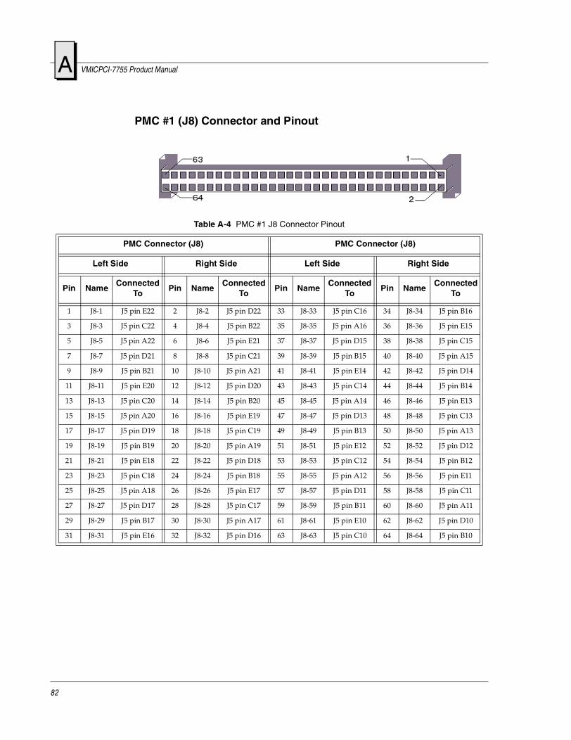
A VMICPCI-7755 Product Manual
PMC #1 (J8) Connector and Pinout
Table A-4 PMC #1 J8 Connector Pinout
PMC Connector (J8) PMC Connector (J8)
Left Side Right Side Left Side Right Side
Pin NameConnected
ToPin Name
ConnectedTo
Pin NameConnected
ToPin Name
ConnectedTo
1 J8-1 J5 pin E22 2 J8-2 J5 pin D22 33 J8-33 J5 pin C16 34 J8-34 J5 pin B16
3 J8-3 J5 pin C22 4 J8-4 J5 pin B22 35 J8-35 J5 pin A16 36 J8-36 J5 pin E15
5 J8-5 J5 pin A22 6 J8-6 J5 pin E21 37 J8-37 J5 pin D15 38 J8-38 J5 pin C15
7 J8-7 J5 pin D21 8 J8-8 J5 pin C21 39 J8-39 J5 pin B15 40 J8-40 J5 pin A15
9 J8-9 J5 pin B21 10 J8-10 J5 pin A21 41 J8-41 J5 pin E14 42 J8-42 J5 pin D14
11 J8-11 J5 pin E20 12 J8-12 J5 pin D20 43 J8-43 J5 pin C14 44 J8-44 J5 pin B14
13 J8-13 J5 pin C20 14 J8-14 J5 pin B20 45 J8-45 J5 pin A14 46 J8-46 J5 pin E13
15 J8-15 J5 pin A20 16 J8-16 J5 pin E19 47 J8-47 J5 pin D13 48 J8-48 J5 pin C13
17 J8-17 J5 pin D19 18 J8-18 J5 pin C19 49 J8-49 J5 pin B13 50 J8-50 J5 pin A13
19 J8-19 J5 pin B19 20 J8-20 J5 pin A19 51 J8-51 J5 pin E12 52 J8-52 J5 pin D12
21 J8-21 J5 pin E18 22 J8-22 J5 pin D18 53 J8-53 J5 pin C12 54 J8-54 J5 pin B12
23 J8-23 J5 pin C18 24 J8-24 J5 pin B18 55 J8-55 J5 pin A12 56 J8-56 J5 pin E11
25 J8-25 J5 pin A18 26 J8-26 J5 pin E17 57 J8-57 J5 pin D11 58 J8-58 J5 pin C11
27 J8-27 J5 pin D17 28 J8-28 J5 pin C17 59 J8-59 J5 pin B11 60 J8-60 J5 pin A11
29 J8-29 J5 pin B17 30 J8-30 J5 pin A17 61 J8-61 J5 pin E10 62 J8-62 J5 pin D10
31 J8-31 J5 pin E16 32 J8-32 J5 pin D16 63 J8-63 J5 pin C10 64 J8-64 J5 pin B10
82

PMC Connector Pinout A
PMC #2 (J12) Connector and Pinout
Table A-5 PMC #2 J12 Connector Pinout
PMC Connector (J12) PMC Connector (J12)
Left Side Right Side Left Side Right Side
Pin NameConnected
ToPin Name
ConnectedTo
Pin NameConnected
ToPin Name
ConnectedTo
1 J12-1 J3 pin E22 2 J12-2 J3 pin D22 33 J12-33 J3 pin C16 34 J12-34 J3 pin B16
3 J12-3 J3 pin C22 4 J12-4 J3 pin B22 35 J12-35 J3 pin A16 36 J12-36 J3 pin E15
5 J12-5 J3 pin A22 6 J12-6 J3 pin E21 37 J12-37 J3 pin D15 38 J12-38 J3 pin C15
7 J12-7 J3 pin D21 8 J12-8 J3 pin C21 39 J12-39 J3 pin B15 40 J12-40 J3 pin A15
9 J12-9 J3 pin B21 10 J12-10 J3 pin A21 41 J12-41 J3 pin E14 42 J12-42 J3 pin D14
11 J12-11 J3 pin E20 12 J12-12 J3 pin D20 43 J12-43 J3 pin C14 44 J12-44 J3 pin B14
13 J12-13 J3 pin C20 14 J12-14 J3 pin B20 45 J12-45 J3 pin A14 46 J12-46 J3 pin E13
15 J12-15 J3 pin A20 16 J12-16 J3 pin E19 47 J12-47 J3 pin D13 48 J12-48 J3 pin C13
17 J12-17 J3 pin D19 18 J12-18 J3 pin C19 49 J12-49 J3 pin B13 50 J12-50 J3 pin A13
19 J12-19 J3 pin B19 20 J12-20 J3 pin A19 51 J12-51 J3 pin E12 52 J12-52 J3 pin D12
21 J12-21 J3 pin E18 22 J12-22 J3 pin D18 53 J12-53 J3 pin C12 54 J12-54 J3 pin B12
23 J12-23 J3 pin C18 24 J12-24 J3 pin B18 55 J12-55 J3 pin A12 56 J12-56 J3 pin E11
25 J12-25 J3 pin A18 26 J12-26 J3 pin E17 57 J12-57 J3 pin D11 58 J12-58 J3 pin C11
27 J12-27 J3 pin D17 28 J12-28 J3 pin C17 59 J12-59 J3 pin B11 60 J12-60 J3 pin A11
29 J12-29 J3 pin B17 30 J12-30 J3 pin A17 61 J12-61 J3 pin E10 62 J12-62 J3 pin D10
31 J12-31 J3 pin E16 32 J12-32 J3 pin D16 63 J12-63 J3 pin C10 64 J12-64 J3 pin B10
83

A VMICPCI-7755 Product Manual
84

Appendix
B
System Driver Software
Contents
Using USB Keyboard/Mouse with Microsoft Windows OSs. . . . . . . . . . . . . . . 86 BIOS Setup . . . . . . . . . . . . . . . . . . . . . . . . . . . . . . . . . . . . . . . . . . . . . . . . . . . . . . . . . 87
Microsoft Windows 98 SE Software Driver Installation . . . . . . . . . . . . . . . . . . . 88 Microsoft Windows NT 4.0 Software Driver Installation . . . . . . . . . . . . . . . . . . 91
Microsoft Windows 2000 Software Driver Installation . . . . . . . . . . . . . . . . . . . . 93 Status of PCI Devices Listed in Windows Device Manager . . . . . . . . . . . . . . . . 95
Introduction
The VMICPCI-7755 provides high-performance video, Ultra ATA storage device control and Local Area Network (LAN) access by means of on-board PCI-based adapters and associated software drivers. High performance video and Ultra ATA storage device control are provided by the embedded Intel 815E chipset. High performance LAN operation, including 10BaseT and 100BaseTx, is provided by the Intel GD82559ER Fast Ethernet adapter chip.
To optimize performance of each of these PCI-based subsystems, the user must install the driver software located on the distribution CD-ROM provided with the unit. Detailed instructions for installation of the drivers during installation of Windows 98 SE, Windows NT (Version 4.0) and Windows 2000 operating systems are described in the following sections.
85

B VMICPCI-7755 Product Manual
Using USB Keyboard/Mouse with Microsoft Windows OSs
This section applies if either a USB keyboard or USB mouse is connected. It does not apply if a PS/2 keyboard and mouse are used.
Windows 98 SE/Windows 2000
The use of a USB keyboard/mouse with an operating system that supports USB devices requires changing the default BIOS settings before and after the installation of Windows 98 SE/2000.
‘Legacy USB Support’ must be enabled in the BIOS to allow a USB keyboard/mouse to operate as a PS/2 device during the installation of Windows 98 SE/2000. After the installation is complete, the computer will restart and actually boot Windows 98 SE/2000. As the computer is restarting to boot the operating system for the first time, ‘Legacy USB Support’ must be disabled and ‘Assign Interrupt to USB’ must be enabled. If Legacy USB Support is not disabled, Windows 98 SE/2000 will attempt to load a device driver for a device (USB) that is not present at that point. See “BIOS Setup” on page 87 for guidelines on changing BIOS settings.
A suggested workaround to this situation is to connect a PS/2 keyboard and mouse, disable ‘Legacy USB Support’ and enable ‘Assign Interrupt to USB’ in the BIOS, and install Windows 98 SE/2000. At some point after the installation is complete, replace the PS/2 keyboard and mouse with a USB keyboard and mouse and make the changed mentioned above to the BIOS. This approach might be easier since you don’t have to worry about making changes to the BIOS at exactly the right time.
Windows NT 4.0
The use of a USB keyboard/mouse with an operating system that does not support USB devices requires changing the default BIOS settings.
‘Legacy USB Support’ must be enabled in the BIOS to allow a USB keyboard/mouse to operate as a PS/2 device. This setting must be enabled prior to the installation and during the operation of Windows NT 4.0. See ‘BIOS Setup’ on page 87 for guidelines on changing BIOS settings.
86

BIOS Setup B
BIOS Setup
To enable/disable Legacy USB Support and/or assign an interrupt to the USB controller, perform the appropriate actions as outlined below:
1. Immediately after the CPU has been powered on or reset, press F2 to enter the ‘Phoenix BIOS Setup Utility’.
2. Using the arrow keys, select the ‘Advanced’ menu.
3. Using the arrow keys, select the ‘Installed OS’ setting. Press + or - on the number keypad to toggle the setting between ‘Other’, ‘Win 95’ and ‘Win 98/Win2000’.
4. Using the arrow keys, select the ‘Assign Interrupt to USB’ setting. Press + or – on the number keypad to toggle the setting between ‘Enabled’ and ‘Disabled’.
NOTE: See “Using USB Keyboard/Mouse with Microsoft Windows Operating Systems” on page 86 for proper setting.
5. Using the arrow keys, select the ‘Legacy USB Support’ setting. Press the + or - keys on the number keypad to toggle the setting between ‘Enabled’ and ‘Disabled’.
6. Press F10 then ENTER to save settings and exit the BIOS.
87

B VMICPCI-7755 Product Manual
Microsoft Windows 98 SE Software Driver Installation
1. Prior to installing Windows 98 SE, ensure the BIOS is set to assign an interrupt to the USB controller. Also ensure ‘Installed OS’ is set to ‘Win98/Win2000’. See ‘BIOS Setup’ on page 87 for guidelines on changing BIOS settings.
2. Begin installation of Windows 98 SE, following the instructions provided by the Windows 98 SE manual.
3. At the ‘Setup Options’ portion of the ‘Windows 98 Setup Wizard’, ensure ‘Typical’ is selected and click ‘Next’.
4. Enter the user ’s name and the company’s name as appropriate and click ‘Next’.
5. At the ‘Windows Components’ portion of the Setup Wizard, ensure ‘Install the most common components’ is selected and click ‘Next’.
6. Continue with the installation until Windows 98 SE is completely installed and has restarted for the last time. Please note that the computer will re-boot several times during the Windows 98 SE installation process.
NOTE: Leave the Windows 98 SE installation CD-ROM in the CD-ROM drive during the entire setup process as additional files may need to be copied.
Intel 815 Chipset Software Installation
1. If not already present, insert the ‘Windows Drivers’ CD-ROM.
2. Click ‘Start’, ‘Run’, ‘Browse’. In the ‘Look in’ pull-down selection menu, select the ‘Windows Drivers’ CD-ROM. Double-click on the ‘Win98’ folder. Double-click on the ‘815chpst’ folder. Double-click on the ‘Disk1’ folder. Double-click on ‘Setup’. Click ‘OK’.
3. At the ‘Welcome’ window, click ‘Next’.
4. Click ‘Yes’ to agree to the software license agreement.
5. Click ‘Next’ at the ‘Readme Information’ window.
6. At the ‘Setup Complete’ window, ensure ‘Yes, I want to restart my computer now’ is selected and click ‘Finish’. The computer will re-boot.
7. Windows 98 SE will find new hardware and install the necessary software. At the ‘System Settings Change’ window, click ‘Yes’ to re-boot the computer.
8. After the unit has re-booted, Windows 98 SE will find additional hardware and present the ‘System Settings Change’ window again. Click ‘Yes’ to re-boot the computer.
88

Microsoft Windows 98 SE Software Driver Installation B
Ultra ATA Storage Driver Installation
1. If not already present, insert the ‘Windows Drivers’ CD-ROM.
2. Click ‘Start’, ‘Run’, ‘Browse’. In the ‘Look in’ pull-down selection menu, select the ‘Windows Drivers’ CD-ROM. Double-click on the ‘Win98’ folder. Double-click on the ‘UltraATA’ folder. Double-click on ‘UltraATA’. Click ‘OK’.
3. At the ‘Intel Ultra ATA storage Driver 6.1 Setup’ window, click ‘Next’. Click ‘Yes’ to agree to the license agreement. Click ‘Next’ twice.
4. Ensure ‘Yes, I want to restart my computer now’ is selected and click ‘Finish’. The computer will re-boot.
Video Driver Installation
1. If not already present, insert the ‘Windows Drivers’ CD-ROM.
2. Click ‘Start’, ‘Run’, ‘Browse’. In the ‘Look in’ pull-down selection menu, select the ‘Windows Drivers’ CD-ROM. Double-click on the ‘Win98’ folder. Double-click on the ‘Video’ folder. Double-click on ‘Setup’. Click ‘OK’.
3. At the ‘Intel 810/810E/815/815E/815EM Chipset Graphics Driver Software Setup’ window, click ‘Next’.
4. Click ‘Yes’ to agree to the software license agreement.
5. Ensure ‘Yes, I want to restart my computer now’ is selected and click ‘Finish’. The computer will re-boot.
Create an Ethernet Adapter Driver Disk
1. Insert a blank floppy disk. The disk will be formatted and files will automatically be copied onto the disk. If not already present, insert the ‘Windows Drivers’ CD-ROM.
2. Click ‘Start’, ‘Run’, ‘Browse’. In the ‘Look in’ pull-down selection menu, select the ‘Windows Drivers’ CD-ROM. Double-click on the ‘LAN’ folder. Double-click on ‘make disk’. Click ‘OK’.
3. Follow the on-screen prompts, then remove the disk and label it ‘Intel GD82559ER Fast ethernet Adapter ’.
4. When the MS-DOS window title changes to ‘Finished-Make disk’, click ’X’ to close the window.
5. Remove the CD-ROM.
Ethernet Adapter Driver Installation
1. Insert the Windows 98 SE installation CD-ROM. Insert the ‘Intel GD82559ER Fast Ethernet Adapter’ floppy disk.
2. Right-click on ‘My Computer ’ and select ‘Properties’. Click on the ‘Device Manager’ tab.
89

B VMICPCI-7755 Product Manual
3. Select ‘PCI Ethernet Controller’ (found under ‘Other devices’) and click ‘Properties’.
4. In the ‘PCI Ethernet Controller Properties’ windows, click on the ‘Driver ’ tab. Click ‘Update Driver’. Click ‘Next’ twice. Ensure ‘Floppy disk drives’ is the only location selected and click ‘Next’.
5. Confirm the ‘Update Device Driver Wizard’ displays ‘Windows driver file search for the device: Intel GD82559ER PCI Adapter ’. Click ‘Next’. If a ‘Copying Files’ window appears asking for the location of the Windows 98 SE CD-ROM, specify the path to the CD-ROM drive containing the Windows 98 SE CD-ROM, (for example d:\) and click ‘OK’. After files have been copied, click ‘Finish’ and remove the floppy disk and CD-ROM.
6. At the ‘System Settings Change’ window that says ‘Do you want to restart your computer now?’, click ‘Yes’.
7. When the computer re-boots, changes can be made to the display and network configurations as desired.
90

Microsoft Windows NT 4.0 Software Driver Installation B
Microsoft Windows NT 4.0 Software Driver Installation
1. Follow the normal Windows NT 4.0 installation until the ‘Windows NT Workstation Setup’ window that states ‘Windows NT needs to know how this computer should participate on a network’ is displayed.
2. Select ‘Do not connect this computer to a network at this time’ and click ‘Next’.
3. Click ‘Finish’.
4. Continue through this portion of Setup. Allow the computer to restart and boot Windows NT.
5. Log on as ‘Administrator ’, using the password provided during the first portion of Setup.
6. Install Service Pack 6a from the CD-ROM provided. Allow the computer to restart and boot Windows NT.
7. Log on as ‘Administrator’.
Ultra ATA Storage Driver Installation
1. If not already present, insert the ‘Windows Drivers’ CD-ROM.
2. Click ‘Start’, ‘Run’, ‘Browse’. In the ‘Look in’ pull-down selection menu, select the ‘Windows Drivers’ CD-ROM. Double-click on the ‘WinNT’ folder. Double-click on the ‘UltraATA’ folder. Double-click on ‘UltraATA’. Click ‘OK’.
3. At the ‘Intel Ultra ATA storage Driver 6.1 Setup’ window, click ‘Next’. Click ‘Yes’ to agree to the license agreement. Click ‘Next’ twice.
4. Ensure ‘Yes, I want to restart my computer now’ is selected and click ‘Finish’. The computer will re-boot.
Video Driver Installation
1. If not already present, insert the ‘Windows Drivers’ CD-ROM.
2. Click ‘Start’, ‘Run’, ‘Browse’. In the ‘Look in’ pull-down selection menu, select the ‘Windows Drivers’ CD-ROM. Double-click on the ‘WinNT’ folder. Double-click on the ‘Video’ folder. Double-click on ‘Setup’ and click ‘OK’.
3. In the ‘Intel 810/810E/815/815E/815EM Chipset Graphics Driver Software Setup’ window, click ‘Next’. Click ‘Yes’ to agree to the license agreement.
4. Select ‘Yes, I want to restart my computer now’ and click ‘Finish’. The computer will re-boot.
Create an Ethernet Adapter Driver Disk
1. Insert a blank floppy disk. The disk will be formatted and files will be automatically copied onto the disk.
91

B VMICPCI-7755 Product Manual
2. If not already present, insert the ‘Windows Drivers’ CD-ROM. Click ‘Start’, ‘Run’, ‘Browse’. In the ‘Look in’ pull-down selection menu, select the ‘Windows Drivers’ CD-ROM. Double-click on the ‘WinNT’ folder. Double-click on the ‘LAN’ folder. Double-click on ‘Makedisk’. Click ‘OK’.
3. Follow the on-screen prompts, then remove the floppy disk and label it ‘Intel GD82559ER Fast Ethernet Adapter’.
4. Remove the CD-ROM.
Ethernet Adapter Driver Installation
1. Insert the ‘Intel GD82559ER Fast Ethernet Adapter ’ driver disk. Insert the Windows NT 4.0 installation CD-ROM. If the ‘Windows NT CD-ROM’ window appears automatically, click ‘X’ to close the window.
2. Click ‘Start’, ‘Settings’, ‘Control Panel’. Double-click on ‘Network’.
3. In the ‘Network Configuration’ window, click ‘Yes’ to install Windows NT Networking.
4. In the ‘Network Setup Wizard’ window, ensure ‘Wired to the network’ is selected and click ‘Next’.
5. Click ‘Select from list’. Click ‘Have Disk’, ‘OK’.
6. In the ‘Select OEM Option’ window, ensure ‘Intel GD82559ER Fast Ethernet Adapter’ is selected and click ‘OK’.
7. In the following window, ensure ‘Intel GD82559ER Fast Ethernet Adapter’ is selected and click ‘Next’.
8. Select the desired protocols and click ‘Next’.
9. Click ‘Next’ two more times.
10. In the ‘Windows NT Setup’ window, enter ‘D:’. If a drive letter other than ‘D’ is assigned to the CD-ROM drive, provide that drive letter in place of ‘D’. Click ‘Continue’.
11. Continue through remaining network setup screens, providing data relative to the network configuration.
12. At ‘Network Settings Change’ window, remove the floppy disk and CD-ROM and click ‘Yes’ to re-boot the computer.
13. When the computer re-boots, log on as ‘Administrator’. A ‘Service Control Manager’ window may appear indicating that a service or driver failed to start. This occurs because during the installation of Windows NT Networking, some updated files were overwritten by files that were copied from the Windows NT 4.0 installation CD-ROM. To fix this issue, re-install Service Pack 6a and re-boot the computer.
92

Microsoft Windows 2000 Software Driver Installation B
Microsoft Windows 2000 Software Driver Installation
1. Prior to installing Windows 2000, ensure the BIOS is set to assign an interrupt to the USB controller. Also ensure ‘Installed O/S’ is set to ‘Win98/Win2000’. See “BIOS Setup” on page 87 for guidelines on changing BIOS settings.
2. Complete the installation of Windows 2000, following the instructions provided by the Windows 2000 manual. Please note that the computer will restart several times during the Windows 2000 installation process.
NOTE: Leave the Windows 2000 installation CD-ROM in the CD-ROM drive during the entire setup process as additional files may need to be copied.
Intel 815 Chipset Software Installation
1. If not already present, insert the Windows Drivers CD-ROM.
2. Click ‘Start’, ‘Run’, ‘Browse’. In the ‘Look in’ pull-down selection menu, select the Windows Drivers CD-ROM. Double-click on the ‘Win2000’ folder. Double-click on the ‘815CPHST’ folder. Double-click on the ‘DISK1’ folder. Double-click on ‘SETUP’. Click ‘OK’.
3. At the ‘Welcome’ window, click ‘Next’.
4. Click ‘Yes’ to agree to the software license agreement.
5. Click ‘Next’ at ‘Readme Information’ window.
6. At the ‘Setup Complete’ window, ensure ‘Yes, I want to restart my computer now’ is selected and click ‘Finish’. Windows 2000 will restart, find new hardware, and install the necessary software.
Ultra ATA Storage Driver Installation
1. If not already present, insert the ‘Windows Drivers’ CD-ROM.
2. Click ‘Start’, ‘Run’, ‘Browse’. In the ‘Look in’ pull-down selection menu, select the ‘Windows Drivers’ CD-ROM. Double-click on the ‘Win2000’ folder. Double-click on the ‘UltraATA’ folder. Double-click on ‘UltraATA’. Click ‘OK’.
3. At the ‘Intel Ultra ATA storage Driver 6.1 Setup’ window, click ‘Next’. Click ‘Yes’ to agree to the license agreement. Click ‘Next’ twice.
4. Ensure ‘Yes, I want to restart my computer now’ is selected and click ‘Finish’. The computer will re-boot.
Video Driver Installation
1. If not already present, insert the ‘Windows Drivers’ CD-ROM.
93

B VMICPCI-7755 Product Manual
2. Click ‘Start’, ‘Run’, ‘Browse’. In the ‘Look in’ pull-down selection menu, select the ‘Windows Drivers’ CD-ROM. Double-click on the ‘Win2000’ folder. Double-click on the ‘Video’ folder. Double-click on ‘Setup’. Click ‘OK’.
3. At the ‘Intel 810/810E/815/815E/815EM Chipset Graphics Drivers’ window, click ‘Next’.
4. In the ‘Save files in folder ’ box, enter the drive letter and path to a temporary directory where the driver files can be stored. (For example, ‘c:\i815temp’.) Click ‘Next’.
5. At the ‘Intel 810/810E/815/815E/815EM Chipset Graphics Driver Software Setup’ window, click ‘Next’.
6. Click ‘Yes’ to agree to the software license agreement.
7. Ensure ‘Yes, I want to restart my computer now’ is selected and click ‘Finish’. The computer will re-boot. The temporary directory created in step 4 can now be safely deleted.
Ethernet Adapter Driver Installation
1. Insert the Windows Drivers CD-ROM.
2. Right-click on ‘My Computer ’ and select ‘Properties’. Click on the ‘Hardware’ tab. Click ‘Device Manager ’.
3. Double-click on ‘Ethernet Controller’ (found under ‘Other devices’).
4. In the ‘Ethernet Controller Properties’ window, click on the ‘Driver’ tab. Click ‘Update Driver ’. Click ‘Next’ twice. Ensure ‘Specify a location’ is the only search location selected (checked) and click ‘Next’.
5. In the ‘Upgrade Device Driver Wizard’ window, click ‘Browse’. In the ‘Look in’ pull-down selection menu, select the Windows Drivers CD-ROM. Double-click on the ‘Win2000’ folder. Double-click on the ‘LAN’ folder. Double-click on ‘OEMSETUP’. Click ‘OK’, then ‘Next’.
6. At the ‘Digital Signature Not Found’ window, click ‘Yes’. After files have been copied, click ‘Finish’ and remove the CD-ROM.
7. At the ‘Intel GD82559ER PCI Adapter Properties’ window, click ‘Close’. Click ‘X’ to close the ‘Device Manager ’ window. Click ‘X’ to close the ‘System Properties’ window.
8. Changes may be made to the network configuration as desired.
94

Status of PCI Devices Listed in Windows Device Manager B
Status of PCI Devices Listed in Windows Device Manager
After installing all of the drivers provided on the Windows Drivers CD-ROM, Device Manager will still indicate that several PCI devices do not have drivers loaded. These devices are the PCI-to-PCI bridge and the VMIC proprietary FPGA. Although these devices are listed as non-functioning by Windows, the hardware is functioning as designed.
95

B VMICPCI-7755 Product Manual
96

Appendix
C
Phoenix BIOS
Contents
Main Menu . . . . . . . . . . . . . . . . . . . . . . . . . . . . . . . . . . . . . . . . . . . . . . . . . . . . . . . . . 99Advanced Menu. . . . . . . . . . . . . . . . . . . . . . . . . . . . . . . . . . . . . . . . . . . . . . . . . . . . . 104Security . . . . . . . . . . . . . . . . . . . . . . . . . . . . . . . . . . . . . . . . . . . . . . . . . . . . . . . . . . . . 108Power . . . . . . . . . . . . . . . . . . . . . . . . . . . . . . . . . . . . . . . . . . . . . . . . . . . . . . . . . . . . . . 109Boot Menu . . . . . . . . . . . . . . . . . . . . . . . . . . . . . . . . . . . . . . . . . . . . . . . . . . . . . . . . . . 110Exit Menu . . . . . . . . . . . . . . . . . . . . . . . . . . . . . . . . . . . . . . . . . . . . . . . . . . . . . . . . . . 111
Introduction
The VMICPCI-7755 utilizes the BIOS (Basic Input/Output System) in the same manner as other PC/AT compatible computers. This appendix describes the menus and options associated with the VMICPCI-7755 BIOS.
System BIOS Setup Utility
During system bootup, press the F2 key to access the Phoenix BIOS Main screen. From this screen, the user can select any section of the Phoenix (system) BIOS for configuration, such as floppy drive configuration or system memory. The parameters shown throughout this section are the default values.
Help Window
The help window on the right side of each menu displays the help text for the currently selected field. It updates as you move the cursor to each field. Pressing F1 or ALT-H on any menu brings up the General Help window that describes the legend keys and their alternates. The scroll bar on the right of any window indicates that there is more than one page of information in the window. Use PGUP and PGDN to display each page. Pressing HOME and END displays the first and last page. Pressing ENTER displays each page. Press ESC to exit the current window.
97

C VMICPCI-7755 Product Manual
First Boot
The VMICPCI-7755 has a First Boot menu enabling the user to, on a one time basis, select a drive device to boot from. This feature is useful when installing from a bootable disk. For example, when installing Windows NT from a CD, enter the First Boot menu and use the arrows keys to highlight ATAPI CD-ROM Drive. Press ENTER to continue with system boot.
This feature is accessed by pressing the ESC at the very beginning of the boot cycle. The selection made from this screen applies to the current boot only, and will not be used during the next boot-up of the system. If you have trouble accessing this feature, disable the QuickBoot Mode in the Main BIOS setup screen. Exit, saving changes and retry accessing the First Boot menu.
%RRW�0HQX
�� ��5HPRYDEOH�'HYLFHV�
�� ��+DUG�'ULYH
�� $7$3,�&'�520�'ULYH
�� 0%$�81',��%XV���6ORW���
�(QWHU�6HWXS!
98

Main Menu C
Main Menu
The Main menu allows the user to select QuickBoot, set the system clock and calendar, record disk drive parameters, and set selected functions for the keyboard.
QuickBoot
When enabled, certain checks normally performed during the POST are omitted, decreasing the time required to run the POST. The default is Enabled.
System Time
The time format is based on the 24-hour military-time clock. For example, 1 PM is 13:00:00. Press the left or right arrow key to move the cursor to the desired field (hour, minute, seconds). Press the PGUP or PGDN key to step through the available choices, or type in the information.
System Date
Press the left or right arrow key to move the cursor to the desired field (month, day, year). Press the PGUP or PGDN key to step through the available choices, or type in the information.
3KRHQL[�6HWXS�8WLOLW\
0$,1 $GYDQFHG 6HFXULW\ 3RZHU %RRW ([LW
,WHP�6SHFLILF�+HOS4XLFN%RRW�0RGH� >(QDEOHG@
6\VWHP�7LPH� >��������@$OORZV�WKH�V\VWHP�WRVNLS�FHUWDLQ�WHVWVZKLOH�ERRWLQJ��7KLVZLOO�GHFUHDVH�WKHWLPH�QHHGHG�WR�ERRWWKH�V\VWHP�
6\VWHP�'DWH� >����������@
/HJDF\�'LVNHWWH�$� >����������0%��òµ@
# 3ULPDU\�0DVWHU >����0%@
# 3ULPDU\�6ODYH >&'�520@
# 6HFRQGDU\�0DVWHU >��0%@
6HFRQGDU\�6ODYH >1RQH@
# .H\ERDUG�)HDWXUHV
# &RQVROH�5HGLUHFWLRQ
6\VWHP�0HPRU\� ����N%
([WHQGHG�0HPRU\� �������N%
([WHQGHG�0HPRU\� ����0%
)�+HOS↑ ↓ 6HOHFW�,WHP���&KDQJH�9DOXHV)�6HWXS�'HIDXOWV(6&([LW← → 6HOHFW�0HQX(QWHU6HOHFW�#�6XE�0HQX)��6DYH�DQG�([LW
99

C VMICPCI-7755 Product Manual
Legacy Diskette
Floppy Drive A
The VMICPCI-7755 supports one floppy disk drive. The options are:
• Disabled No diskette drive installed• 360K, 5.25 in 5-1/4 inch PC-type standard drive; 360 kilobyte capacity
• 1.2M, 5.25 in 5-1/4 inch AT-type high-density drive; 1.2 megabyte capacity• 720K, 3.5 in 3-1/2 double-sided drive; 720 kilobyte capacity
• 1.44M, 3.5 in 3-1/2 inch double-sided drive; 1.44 megabyte capacity• 2.88M, 3.5 in 3-1/2 inch double-sided drive; 2.88 megabyte capacity
Use PGUP or PGDN to select the floppy drive. The default is 1.44M, 3.5 inch.
Primary Master/Slave
The VMICPCI-7755 is capable of utilizing one IDE hard disk drive on the Primary Master bus. The default setting is Auto. The Primary Slave is assigned to the CD-ROM (if installed). If a setting other than Auto is selected the user must match the settings to the hardware.
3KRHQL[�6HWXS�8WLOLW\
0$,1
,WHP�6SHFLILF�+HOS3ULPDU\�0DVWHU�>����@
8VHU� �\RX�HQWHUSDUDPHWHUV�RI�KDUG�GLVNGULYH�LQVWDOOHG�DW�WKLVFRQQHFWLRQ�$XWR� �DXWRW\SHV�KDUG�GULYHLQVWDOOHG�KHUH������ �\RX�VHOHFW�SUH�GHWHUPLQHG�W\SH�RIKDUG�GULYHLQVWDOOHG�KHUH�&'�520� �D�&'�520�GULYHLV�LQVWDOOHG�KHUH�$7$3,�5HPRYDEOH� �5HPRYDEOH�GLVN�GULYH�LVLQVWDOOHG�KHUH�
7\SH� >$XWR@
0XOWL�6HFWRU�7UDQVIHUV >���6HFWRUV@
/%$�0RGH�&RQWURO >(QDEOHG@
���%LW�,�2 >'LVDEOHG@
7UDQVIHU�0RGH� >)DVW�3,2��@
8OWUD�'0$�0RGH� >0RGH��@
)�+HOS↑ ↓ 6HOHFW�,WHP���&KDQJH�9DOXHV)�6HWXS�'HIDXOWV(6&([LW← → 6HOHFW�0HQX(QWHU6HOHFW�#�6XE�0HQX)��6DYH�DQG�([LW
100

Main Menu C
Secondary Master
The Secondary Master is the resident Flash Disk (if installed). The default setting is Auto.
Keyboard Features
The Keyboard Features allows the user to set several keyboard functions.
NumLock
The NumLock can be set to Auto, On or Off to control the state of the NumLock key when the system boots. When set to Auto or On, the numeric keypad generates numbers instead of controlling the cursor operations. The default is Auto.
Key Click
This option enables or disables the Keyboard Auto-Repeat Rate and Delay settings. When disabled, the values in the Typematic Rate and Delay are ignored. The default is Disabled.
Keyboard Auto-Repeat Rate (Chars/Sec)
If the Key Click is enabled this determines the rate a character is repeated when a key is held down. The options are: 30, 26.7, 21.8, 18.5, 13.3, 10, 6 or 2 characters per second. The default is 30.
3KRHQL[�6HWXS�8WLOLW\
0$,1
,WHP�6SHFLILF�+HOS.H\ERDUG�)HDWXUHV
6HOHFWV�3RZHU�RQ�VWDWHIRU�1XP/RFN�
1XP/RFN� >$XWR@
.H\�&OLFN� >'LVDEOHG@
.H\ERDUG�$XWR�5HSHDW�5DWH� >���VHF@
.H\ERDUG�$XWR�5HSHDW�'HOD\�>����VHF@
.H\ERDUG�7HVW >'LVDEOHG@
)�+HOS↑ ↓ 6HOHFW�,WHP���&KDQJH�9DOXHV)�6HWXS�'HIDXOWV(6&([LW← → 6HOHFW�0HQX(QWHU6HOHFW�#�6XE�0HQX)��6DYH�DQG�([LW
101

C VMICPCI-7755 Product Manual
Keyboard Auto-Repeat Delay (sec)
If the Key Click is enabled, this determines the delay before a character starts repeating when a key is held down. The options are: 1/4, 1/2, 3/4 or 1 second. The default is 1/2.
Keyboard Test
When enabled, this feature will test the keyboard during boot-up.
Console Redirection
Console Redirection allows for remote access and control of the PC functions to a remote terminal via the serial port. Selecting Console Redirection provides additional menus used to configure the console.
Com Port AddressIf enabled, it will allow remote access through the serial port. The options are: Disabled, Motherboard Com A and Motherboard Com B. The default is Disabled.
Baud RateSelects a baud rate for the serial port. The options are: 600, 1200, 2400, 4800, 9600, 19.2, 38.4 and 115.2. The default is 19.2.
Console TypeSelects the type of console to be used. The options are: PC ANSI or VT100. The default is PC ANSI.
3KRHQL[�6HWXS�8WLOLW\
0$,1
,WHP�6SHFLILF�+HOS&RQVROH�5HGLUHFWLRQ
,I�HQDEOHG��LW�ZLOOXVH�D�SRUW�RQ�WKH�PRWKHUERDUG�
&RP�3RUW�$GGUHVV >'LVDEOHG@
%DXG�5DWH >����@
&RQVROH�7\SH >3&�$16,@
)ORZ�&RQWURO >&76�576@
&RQVROH�FRQQHFWLRQ� >'LUHFW@
&RQWLQXH�&�5��$IWHU�3267� >2II@
)�+HOS↑ ↓ 6HOHFW�,WHP���&KDQJH�9DOXHV)�6HWXS�'HIDXOWV(6&([LW← → 6HOHFW�0HQX(QWHU6HOHFW�#�6XE�0HQX)��6DYH�DQG�([LW
102

Main Menu C
Flow ControlEnables or disables Flow Control. The options are No Flow Control, XON/XOFF or CTS/RTS. The default is CTS/RTS.
Console ConnectionIndicates whether the console is connected directly to the system, or if a modem is being used to connect. The options are: Direct or Via Modem. The default is Direct.
Continue C.R. After POSTThis enables console redirection after the operating system has loaded. The options are OFF or ON. The default setting is OFF.
System Memory
The System Memory field is for informational purposes only and cannot be modified by the user. This field displays the base memory installed in the system.
Extended Memory
The Extended Memory field is for informational purposes only and cannot be modified by the user. This field displays the total amount of memory installed in the system in Kbytes.
Extended Memory
The Extended Memory field is for informational purposes only and cannot be modified by the user. This field displays the total amount of memory installed in the system in Mbytes.
103

C VMICPCI-7755 Product Manual
Advanced Menu
Selecting Advanced from the Main menu will display the screen shown below.
Advanced Chipset Control
Selecting Advanced Chipset Control opens the menu below. Use this menu to change the values in the chipset register for optimizing your system’s performance.
3KRHQL[�6HWXS�8WLOLW\
0DLQ $'9$1&(' 6HFXULW\ 3RZHU %RRW ([LW
,WHP�6SHFLILF�+HOS# $GYDQFHG�&KLSVHW�&RQWURO
# &DFKH�0HPRU\6HOHFW�WKH�RSHUDWLQJV\VWHP�LQVWDOOHGRQ�\RXU�V\VWHP�ZKLFK\RX�ZLOO�XVH�PRVWFRPPRQO\�
1RWH��$Q�LQFRUUHFWVHWWLQJ�FDQ�FDXVHVRPH�RSHUDWLQJV\VWHPV�WR�GLVSOD\XQH[SHFWHG�EHKDYLRU�
# ,�2�'HYLFH�&RQILJXUDWLRQ
5HVHW�&RQILJXUDWLRQ�'DWD >1R@
,QVWDOOHG�2�6� >2WKHU@
/DUJH�'LVN�$FFHVV�0RGH� >'26@
/%$�$VVLVWHG�7UDQVODWLRQ >'LVDEOHG@
/RFDO�%XV�,'(�DGDSWHU� >%RWK@
$VVLJQ�,QWHUUXSW�7R�86% >(QDEOHG@
/HJDF\�86%�6XSSRUW >'LVDEOHG@
&DUG%XV�%ULGJH�0HPRU\�6L]H >����NE\WH@
3267�(UURUV >(QDEOHG@
)RUFH�+DUG�UHVHW >'LVDEOHG@
)�+HOS↑ ↓ 6HOHFW�,WHP���&KDQJH�9DOXHV)�6HWXS�'HIDXOWV(6&([LW← → 6HOHFW�0HQX(QWHU6HOHFW�#�6XE�0HQX)��6DYH�DQG�([LW
3KRHQL[�6HWXS�8WLOLW\
$'9$1&('
,WHP�6SHFLILF�+HOS$GYDQFHG�&KLSVHW�&RQWURO
6HOHFW�¶2QERDUG�9LGHR·WR�HQDEOH�WKH�RQERDUGYLGHR�FRQWUROOHU�DVWKH�ERRW�GLVSOD\GHYLFH��6HOHFW�HLWKHU���N�RU���0%�RI�6\VWHP0HPRU\�WR�EH�DOORFDWHGWR�WKH�RQERDUG�YLGHRFRQWUROOHU�
6HOHFW¶'LVDEOH�2QERDUG�9LGHR·WR�GLVDEOH�WKH�RQERDUGYLGHR�FRQWUROOHU��1R6\VWHP�0HPRU\�ZLOO�EHDOORFDWHG�IRU�YLGHR�
9LGHR�ERRW�W\SH >2QERDUG�9LGHR@
(QDEOH�PHPRU\�JDS� >'LVDEOHG@
)�+HOS↑ ↓ 6HOHFW�,WHP���&KDQJH�9DOXHV)�6HWXS�'HIDXOWV(6&([LW← → 6HOHFW�0HQX(QWHU6HOHFW�#�6XE�0HQX)��6DYH�DQG�([LW
104

Advanced Menu C
Video Boot Type
Select “Onboard Video’ to enable the onboard video controller as the boot display device. Select “Disable Onboard Video’ to disable the onboard video controller.
Enable Memory Gap
If enabled, turn system RAM off to free address space for use with an option card. Either a 128KB conventional memory gap, starting at 512KB, or a 1MB extended memory gap, starting at 15MB, will be created in the system RAM. The options are Disabled, Conventional or Extended. The default is Disabled.
Cache Memory
Enabling the cache memory enhances the speed of the processor. When the CPU requests data, the system transfers the requested data from the main DRAM into the cache memory where it is stored until processed by the CPU. The default is Enabled.
3KRHQL[�6HWXS�8WLOLW\
$'9$1&('
,WHP�6SHFLILF�+HOS&DFKH�0HPRU\
6HWV�WKH�VWDWH�RI�WKHPHPRU\�FDFKH
0HPRU\�&DFKH >(QDEOHG@
&DFKH�6\VWHP�%,26�DUHD� >:ULWH�3URWHFW@
&DFKH�9LGHR�%,26�DUHD� >:ULWH�3URWHFW@
&DFKH�%DVH������N� >:ULWH�%DFN@
&DFKH�%DVH����N����N� >:ULWH�%DFN@
&DFKH�([WHQGHG�0HPRU\�$UHD� >:ULWH�%DFN@
&DFKH�$����$)))� >'LVDEOHG@
&DFKH�%����%)))� >'LVDEOHG@
&DFKH�&����&%))� >:ULWH�7KURXJK@
&DFKH�&&���&)))� >:ULWH�7KURXJK@
&DFKH�'����'�))� >:ULWH�7KURXJK@
&DFKH�'����'�))� >:ULWH�7KURXJK@
&DFKH�'����'%))� >:ULWH�7KURXJK@
&DFKH�'&���'))) >:ULWH�7KURXJK@
&DFKH�(����(�)) >:ULWH�7KURXJK@
)�+HOS↑ ↓ 6HOHFW�,WHP���&KDQJH�9DOXHV)�6HWXS�'HIDXOWV(6&([LW← → 6HOHFW�0HQX(QWHU6HOHFW�#�6XE�0HQX)��6DYH�DQG�([LW
105

C VMICPCI-7755 Product Manual
I/O Device Configuration
Select this menu to configure your I/O devices, if required.
Reset Configuration Data
Select Yes if you want to clear the extended system configuration data. The default is No.
Installed O/S
Use this feature to select the operating system to use with your system.
Large Disk Access Mode
The options for the Large Disk Access Mode are UNIX Novell Netware or Other.
If you are installing new software and the drive fails, change this selection and try again. Different operating systems require different representations of drive geometries. The default is DOS.
LBA Assisted Translation
LBA (Logical Block Addressing): During drive accesses, the IDE controller transforms the data address described by sector, head, and cylinder number into a physical block address. This significantly improves data transfer rates for drives with greater than 1024 cylinders. The default is Disabled.
3KRHQL[�6HWXS�8WLOLW\
$'9$1&('
,WHP�6SHFLILF�+HOS,�2�'HYLFH�&RQILJXUDWLRQ
&RQILJXUH�VHULDO�SRUW�$XVLQJ�RSWLRQV�
>'LVDEOHG@1R�&RQILJXUDWLRQ
>(QDEOHG@8VHU�&RQILJXUDWLRQ
>$XWR@%,26�RU�26�FKRRVHV�26�&RQWUROOHG�'LVSOD\HG�ZKHQFRQWUROOHG�E\�26
6HULDO�SRUW�$� >$XWR@
6HULDO�SRUW�%� >$XWR@
)ORSS\�GLVN�FRQWUROOHU� >(QDEOHG@
36���0RXVH >$XWR�'HWHFW@
)�+HOS↑ ↓ 6HOHFW�,WHP���&KDQJH�9DOXHV)�6HWXS�'HIDXOWV(6&([LW← → 6HOHFW�0HQX(QWHU6HOHFW�#�6XE�0HQX)��6DYH�DQG�([LW
106

Advanced Menu C
Local Bus IDE Adapter
This enables or disables the intergrated local bus IDE adapter. The options are: Disabled, Primary, Secondary or Both. The default is Both.
Assign Interrupt To USB
Enabled assigns an interrupt to the USB. The default is Enabled.
Legacy USB Support
Enabled supports a legacy keyboard and mouse on the USB. The default is Disabled.
Cardbus Memory Size
When enabled, allows resources to be allocated from a Cardbus controller located behind a PCI-to-PCI Bridge. When enabled the screen will show the amount allocated. The default is Enabled.
POST Errors
Pauses and displays Setup Entry or Resume Boot prompt if an error occurs on boot. If disabled, the prompt will be bypassed and the system will attempt to boot. The default is Enabled.
Force Hard Reset
A reboot causes a warm restart which does not issue board resets and executes only a subset of BIOS POST to reduce boot time. If an OS reboot causes boot failure or a PCI device requires a reset, enable this function to force a hard reset during reboot. The default is Disabled.
107

C VMICPCI-7755 Product Manual
Security
Utilize this screen to set a user password.
Password On Boot
Enables password entry on boot. The default is Disabled.
Fixed Disk Sector
Write protects boot sector on the hard disk to protect against viruses. The default is Normal.
Diskette Access
Controls access to the diskette drives. The default is User.
3KRHQL[�6HWXS�8WLOLW\
6HFXULW\
,WHP�6SHFLILF�+HOS6HFXULW\
6XSHUYLVRU�3DVVZRUGFRQWUROV�$FFHVV�WR�WKHVHWXS�XWLOLW\�
���6HW�8VHU�3DVVZRUG >�(QWHU�@
���6HW�6XSHUYLVRU�3DVVZRUG >(QWHU@
���3DVVZRUG�RQ�ERRW� >'LVDEOHG@
���)L[HG�GLVN�ERRW�VHFWRU >1RUPDO@
���'LVNHWWH�DFFHVV���� >8VHU@
)�+HOS↑ ↓ 6HOHFW�,WHP���&KDQJH�9DOXHV)�6HWXS�'HIDXOWV(6&([LW← → 6HOHFW�0HQX(QWHU6HOHFW�#�6XE�0HQX)��6DYH�DQG�([LW
108

Power C
Power
This screen, selected from the Main screen, allows the user to configure power saving options on the VMICPCI-7755.
The Throttling and CPU Throttling back hysteresis selections will only be shown if CPU DIE Temp is enabled. The default for Throttling is 50%. The default for CPU Throttling back hysteresis is 10C.
3KRHQL[�6HWXS�8WLOLW\
0DLQ $GYDQFHG 6HFXULW\ 32:(5 %RRW ([LW
,WHP�6SHFLILF�+HOS&38�7KURWWOLQJ�'RZQ�7KUHVKROG >'LVDEOHG@
&38�7KURWWOLQJ�EDFN�K\VWHUHVLV >��&@0D[LPXP�3RZHU�VDYLQJVFRQVHUYHV�WKH�JUHDWHVWDPRXQW�RI�V\VWHP�SRZHU�0D[LPXP�3HUIRUPDQFHFRQVHUYHV�SRZHU�EXWDOORZV�JUHDWHVW�V\VWHPSHUIRUPDQFH��7R�DOWHUWKHVH�VHWWLQJV��FKRRVH&XVWRPL]HG��7R�WXUQ�RII�SRZHU�PDQDJHPHQW�FKRRVH�'LVDEOHG�
7KURWWOLQJ�� >���@
3RZHU�6DYLQJV� >'LVDEOHG@
:DNHXS�7LPH� >2II@
5HVXPH�7LPH� >��������@
)�+HOS↑ ↓ 6HOHFW�,WHP���&KDQJH�9DOXHV)�6HWXS�'HIDXOWV(6&([LW← → 6HOHFW�0HQX(QWHU6HOHFW�#�6XE�0HQX)��6DYH�DQG�([LW
109

C VMICPCI-7755 Product Manual
Boot Menu
The Boot priority is determined by the stack order, with the top having the highest priority and the bottom the least. The order can be modified by highlighting a device and, using the <+> or <-> keys, moving it to the desired order in the stack. A device can be boot disabled by highlighting the particular device and pressing <Shift 1>. <Enter> expands or collapses devices with a + or - next to them.
3KRHQL[�6HWXS�8WLOLW\
0$,1 $GYDQFHG 6HFXULW\ 3RZHU %RRW ([LW
,WHP�6SHFLILF�+HOS��5HPRYDEOH�'HYLFHV�
��+DUG�'ULYH.H\V�XVHG�WR�YLHZ�RUFRQILJXUH�GHYLFHV��(QWHU!�H[SDQGV�RUFROODSVHV�GHYLFHV�ZLWKD���RU���&WUO���(QWHU!�H[SDQGVDOO�6KLIW����!�HQDEOHV�RUGLVDEOHV�D�GHYLFH���!�DQG���!�PRYHV�WKH�GHYLFH�XS�RU�GRZQ��Q!�PD\�PRYH�UHPRYDEOHGHYLFH�EHWZHHQ�+DUG�'LVN�RU�5HPRYDEOH�'LVN�G!�UHPRYH�D�GHYLFHWKDW�LV�QRW�LQVWDOOHG�
��&'�520�'ULYH
��0%$�81',��%XV��6ORW��
)�+HOS↑ ↓ 6HOHFW�,WHP���&KDQJH�9DOXHV)�6HWXS�'HIDXOWV(6&([LW← → 6HOHFW�0HQX(QWHU6HOHFW�#�6XE�0HQX)��6DYH�DQG�([LW
110
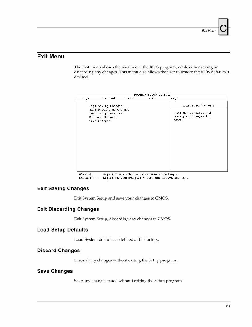
Exit Menu C
Exit Menu
The Exit menu allows the user to exit the BIOS program, while either saving or discarding any changes. This menu also allows the user to restore the BIOS defaults if desired.
Exit Saving Changes
Exit System Setup and save your changes to CMOS.
Exit Discarding Changes
Exit System Setup, discarding any changes to CMOS.
Load Setup Defaults
Load System defaults as defined at the factory.
Discard Changes
Discard any changes without exiting the Setup program.
Save Changes
Save any changes made without exiting the Setup program.
3KRHQL[�6HWXS�8WLOLW\
0DLQ $GYDQFHG 3RZHU %RRW ([LW
,WHP�6SHFLILF�+HOS([LW�6DYLQJ�&KDQJHV
([LW�'LVFDUGLQJ�&KDQJHV([LW�6\VWHP�6HWXS�DQGVDYH�\RXU�FKDQJHV�WR&026�
/RDG�VHWXS�'HIDXOWV
'LVFDUG�&KDQJHV
6DYH�&KDQJHV
)�+HOS↑ ↓ 6HOHFW�,WHP���&KDQJH�9DOXHV)�6HWXS�'HIDXOWV(6&([LW← → 6HOHFW�0HQX(QWHU6HOHFW�#�6XE�0HQX)��6DYH�DQG�([LW
111

C VMICPCI-7755 Product Manual
112

Appendix
D
LANWorks BIOS
Contents
Boot Menus . . . . . . . . . . . . . . . . . . . . . . . . . . . . . . . . . . . . . . . . . . . . . . . . . . . . . . . . 114BIOS Features Setup . . . . . . . . . . . . . . . . . . . . . . . . . . . . . . . . . . . . . . . . . . . . . . . . . 116
Introduction
The VMICPCI-7755 includes a LANWorks option which allows the VMICPCI-7755 to be booted from a network. This appendix describes the procedures to enable this option and the LANWorks BIOS Setup screens.
113

D VMICPCI-7755 Product Manual
Boot Menus
There are two methods of enabling the LANWorks BIOS option. The first method is the First Boot menu. The second is the Boot menu from the BIOS Setup Utility.
First Boot Menu
Press ESC at the very beginning of the boot cycle, which will access the First Boot menu. Selecting “Managed PC Boot Agent (MBA)” to boot from the LAN in this screen applies to the current boot only, at the next re-boot the VMICPCI-7755 will revert back to the setting in the Boot menu.
Using the arrow keys, highlight Managed PC Boot Agent (MBA), and press the ENTER key to continue with the system boot.
Boot Menu
The second method of enabling the LANWorks BIOS option is to press the F2 key during system boot. This will access the BIOS Setup Utility. Advance to the Boot menu and, using the arrow keys, highlight the Managed PC Boot Agent (MBA) option. Repeat entering <+> until MBA is at the top of the list.
Advance to the Exit menu, select “Exit Saving Changes” and press ENTER. When the system prompts for confirmation, press “Yes”. The computer will then restart the system boot-up.
%RRW�0HQX
��5HPRYDEOH�'HYLFHV�
��+DUG�'ULYH
$7$3,�&'�520�'ULYH
0DQDJHG�3&�%RRW�$JHQW��0%$�
�(QWHU�6HWXS!
114

Boot Menus D
3KRHQL[�6HWXS�8WLOLW\
0$,1 $GYDQFHG 6HFXULW\ 3RZHU %RRW ([LW
,WHP�6SHFLILF�+HOS0DQDJHG�3&�%RRW�$JHQW��0%$�
��5HPRYDEOH�'HYLFHV�.H\V�XVHG�WR�YLHZ�RUFRQILJXUH�GHYLFHV��(QWHU!�H[SDQGV�RUFROODSVHV�GHYLFHV�ZLWKD���RU���&WUO���(QWHU!�H[SDQGVDOO�6KLIW����!�HQDEOHV�RUGLVDEOHV�D�GHYLFH���!�DQG���!�PRYHV�WKH�GHYLFH�XS�RU�GRZQ��Q!�PD\�PRYH�UHPRYDEOHGHYLFH�EHWZHHQ�+DUG�'LVN�RU�5HPRYDEOH�'LVN�G!�UHPRYH�D�GHYLFHWKDW�LV�QRW�LQVWDOOHG�
��+DUG�'ULYH
��$7$3,�&'�520�'ULYH
��5HPRYDEOH�'HYLFHV�
)�+HOS↑ ↓ 6HOHFW�,WHP���&KDQJH�9DOXHV)�6HWXS�'HIDXOWV(6&([LW← → 6HOHFW�0HQX(QWHU6HOHFW�#�6XE�0HQX)��6DYH�DQG�([LW
115
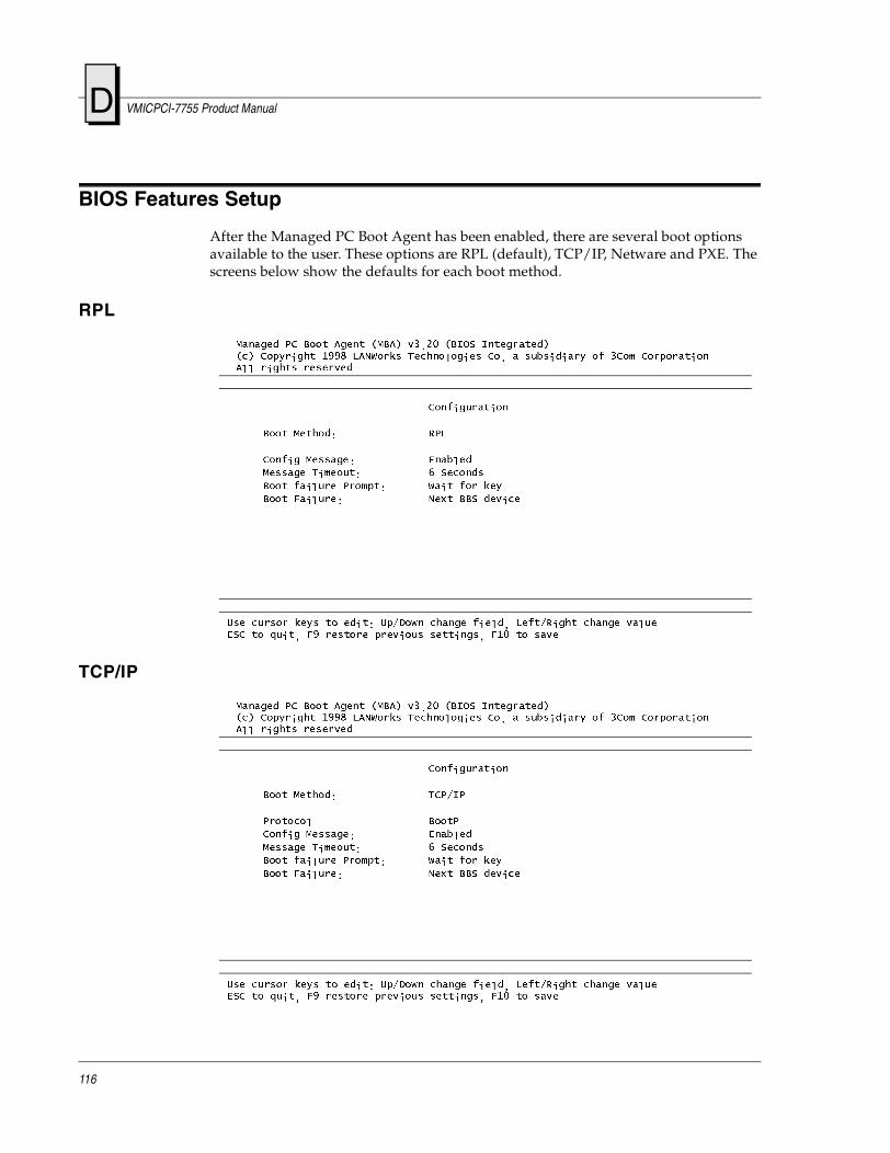
D VMICPCI-7755 Product Manual
BIOS Features Setup
After the Managed PC Boot Agent has been enabled, there are several boot options available to the user. These options are RPL (default), TCP/IP, Netware and PXE. The screens below show the defaults for each boot method.
RPL
TCP/IP
0DQDJHG�3&�%RRW�$JHQW��0%$��Y������%,26�,QWHJUDWHG��F��&RS\ULJKW������/$1:RUNV�7HFKQRORJLHV�&R��D�VXEVLGLDU\�RI��&RP�&RUSRUDWLRQ$OO�ULJKWV�UHVHUYHG
&RQILJXUDWLRQ
%RRW�0HWKRG� 53/
&RQILJ�0HVVDJH� (QDEOHG
0HVVDJH�7LPHRXW� ��6HFRQGV
%RRW�IDLOXUH�3URPSW� :DLW�IRU�NH\
%RRW�)DLOXUH� 1H[W�%%6�GHYLFH
8VH�FXUVRU�NH\V�WR�HGLW��8S�'RZQ�FKDQJH�ILHOG��/HIW�5LJKW�FKDQJH�YDOXH(6&�WR�TXLW��)��UHVWRUH�SUHYLRXV�VHWWLQJV��)���WR�VDYH
0DQDJHG�3&�%RRW�$JHQW��0%$��Y������%,26�,QWHJUDWHG��F��&RS\ULJKW������/$1:RUNV�7HFKQRORJLHV�&R��D�VXEVLGLDU\�RI��&RP�&RUSRUDWLRQ$OO�ULJKWV�UHVHUYHG
&RQILJXUDWLRQ
%RRW�0HWKRG� 7&3�,3
3URWRFRO %RRW3
&RQILJ�0HVVDJH� (QDEOHG
0HVVDJH�7LPHRXW� ��6HFRQGV
%RRW�IDLOXUH�3URPSW� :DLW�IRU�NH\
%RRW�)DLOXUH� 1H[W�%%6�GHYLFH
8VH�FXUVRU�NH\V�WR�HGLW��8S�'RZQ�FKDQJH�ILHOG��/HIW�5LJKW�FKDQJH�YDOXH(6&�WR�TXLW��)��UHVWRUH�SUHYLRXV�VHWWLQJV��)���WR�VDYH
116

BIOS Features Setup D
Netware
PXE
0DQDJHG�3&�%RRW�$JHQW��0%$��Y������%,26�,QWHJUDWHG��F��&RS\ULJKW������/$1:RUNV�7HFKQRORJLHV�&R��D�VXEVLGLDU\�RI��&RP�&RUSRUDWLRQ$OO�ULJKWV�UHVHUYHG
&RQILJXUDWLRQ
%RRW�0HWKRG� 1HWZDUH
3URWRFRO �����
&RQILJ�0HVVDJH� (QDEOHG
0HVVDJH�7LPHRXW� ��6HFRQGV
%RRW�IDLOXUH�3URPSW� :DLW�IRU�NH\
%RRW�)DLOXUH� 1H[W�%%6�GHYLFH
8VH�FXUVRU�NH\V�WR�HGLW��8S�'RZQ�FKDQJH�ILHOG��/HIW�5LJKW�FKDQJH�YDOXH(6&�WR�TXLW��)��UHVWRUH�SUHYLRXV�VHWWLQJV��)���WR�VDYH
0DQDJHG�3&�%RRW�$JHQW��0%$��Y������%,26�,QWHJUDWHG��F��&RS\ULJKW������/$1:RUNV�7HFKQRORJLHV�&R��D�VXEVLGLDU\�RI��&RP�&RUSRUDWLRQ$OO�ULJKWV�UHVHUYHG
&RQILJXUDWLRQ
%RRW�0HWKRG� 3;(
8VH�FXUVRU�NH\V�WR�HGLW��8S�'RZQ�FKDQJH�ILHOG��/HIW�5LJKW�FKDQJH�YDOXH(6&�WR�TXLW��)��UHVWRUH�SUHYLRXV�VHWWLQJV��)���WR�VDYH
117

D VMICPCI-7755 Product Manual
118
Appendix
E
Sample C Software
Contents
Directory \21154 . . . . . . . . . . . . . . . . . . . . . . . . . . . . . . . . . . . . . . . . . . . . . . . . . . . . 119 Directory \fpga . . . . . . . . . . . . . . . . . . . . . . . . . . . . . . . . . . . . . . . . . . . . . . . . . . . . . 119
Directory \i2c . . . . . . . . . . . . . . . . . . . . . . . . . . . . . . . . . . . . . . . . . . . . . . . . . . . . . . 120 Directory \include . . . . . . . . . . . . . . . . . . . . . . . . . . . . . . . . . . . . . . . . . . . . . . . . . . 120
Directory \max1617 . . . . . . . . . . . . . . . . . . . . . . . . . . . . . . . . . . . . . . . . . . . . . . . . . 120 Directory \support . . . . . . . . . . . . . . . . . . . . . . . . . . . . . . . . . . . . . . . . . . . . . . . . . . 120
Directory \vlm . . . . . . . . . . . . . . . . . . . . . . . . . . . . . . . . . . . . . . . . . . . . . . . . . . . . . 120
Introduction
This appendix provides listings of a library of sample code that the programmer may utilize to build applications. These files are provided in the directory “\sample code” on CD 320-500077-000, labeled “Windows Drivers”, included with the VMICPCI-7755.
These files are provided without warranty. All source code is 2001, VMIC Corporation.
Directory \21154
This directory contains code used to test accesses across the CompactPCI bus between a peripheral CPU card (for example, the VMICPCI-7756) and a system controller CPU (for example, the VMICPCI-7755).
Directory \fpga
This directory contains code used to test the functions of the VMIC-designed FPGA such as timers, SRAM controller and Watchdog Timer.
119

E VMICPCI-7755 Product Manual
Directory \i2c
This directory contains code that demonstrates how to send data using the I2C controller in the super I/O component and also how to manipulate the I2C mux which is used to direct the super I/O’s I2C back to the CompactPCI backplane.
Directory \include
This directory contains common files required to compile several of the sample code applications.
Directory \max1617
This directory contains code that demonstrates how to read the temperatures from the max1617 device on the VMICPCI-7755.
Directory \support
This directory contains memory and PCI access routines used by many of the sample code applications.
Directory \vlm
This directory contains code that demonstrates how to read the voltages from the analog inputs of the super I/O component on the VMICPCI-7755.
120

Appendix
F
Serial ROM for the 21154
Introduction
The VMICPCI-7755 is shipped with a default configuration for the SROM used to load the 21154 Embedded PCI bridge chip at power up and reset.
The contents of the SROM are as follows:
VMICPCI-7755 21154 SROM Code
;Preload enable (bit 7 set for preload enable)
:00 80
:01 00
:02 00
:03 00
;Primary Class Code
:04 00
:05 80
:06 06
;Subvendor IDs
:07 55
:08 77
:09 4A
:0A 11
;Primary Min GNT, Max Lat
:0B 00
:0C 00
121
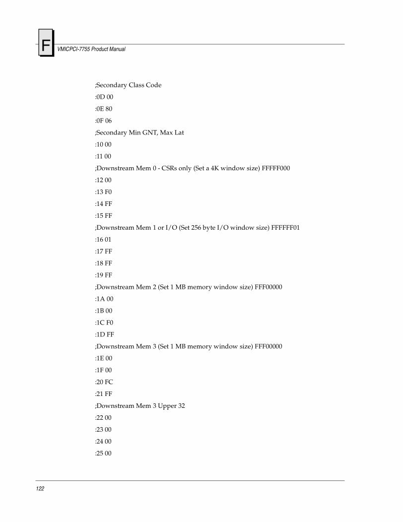
F VMICPCI-7755 Product Manual
;Secondary Class Code
:0D 00
:0E 80
:0F 06
;Secondary Min GNT, Max Lat
:10 00
:11 00
;Downstream Mem 0 - CSRs only (Set a 4K window size) FFFFF000
:12 00
:13 F0
:14 FF
:15 FF
;Downstream Mem 1 or I/O (Set 256 byte I/O window size) FFFFFF01
:16 01
:17 FF
:18 FF
:19 FF
;Downstream Mem 2 (Set 1 MB memory window size) FFF00000
:1A 00
:1B 00
:1C F0
:1D FF
;Downstream Mem 3 (Set 1 MB memory window size) FFF00000
:1E 00
:1F 00
:20 FC
:21 FF
;Downstream Mem 3 Upper 32
:22 00
:23 00
:24 00
:25 00
122

F
;Expansion ROM (Set 1 MB expansion ROM size)
:26 01
:27 F0
;Upstream Mem 0 or I/O (Set 256 byte I/O window size) FFFFFF01
:28 01
:29 FF
:2A FF
:2B FF
;Upstream Mem 1 (Set 256 MB memory window size) F0000000
:2C 00
:2D 00
:2E 00
:2F F0
;Chip Control 0
:30 00
;Clear lockout bit
:31 00
;Chip Control 1
:32 00
;LUT disable, I2O disable
:33 90
;Arbiter control (Sets internal 21154 secondary bus req. to high priority ring)
:34 00
:35 02
;System error disable
:36 00
:37 00
;Power management
:38 00
:39 00
:3A 00
:3B 00
123

F VMICPCI-7755 Product Manual
:3C 00
:3D 00
:3E 00
:3F 00
:40 00
:41 00
:42 00
Upstream or Outbound means going out to the CompactPCI backplane from the local processor, Downstream or Inbound means coming into the local CPU bus from the CompactPCI backplane.
The CPCI-7755, 21154 bridge will be programmed as follows:
The outbound memory window is 256MBytes, inbound is 1MByte.
Both I/O windows are 256 bytes, inbound and outbound.
Address translation registers power up at 0 values such that the mapping forces the absolute address to 0 for outbound and inbound memory and I/O windows.
The user MUST load program translation offset registers if a value other than zero is required.
124

Index
Numerics100BaseTx 49, 7710BaseT 49, 77
BBIOS 31, 44BIOS setup 87BIOS setup screens 97
CCMOS configuration 31connectors 26CPU board diagram 27Customer Service 26
DDMA controller 39DMA page registers 39
Eethernet adapter driver 89ethernet driver 91
FFirst Boot 98Floppy Disk Drive 100Floppy Drive A 100
II/O
address space 39port map 39
installation 30Intel 815 Chipset 88Intel 82559 Ethernet Controller 49interrupt line assignment 41
Jjumper locations 27
LLPT1 Parallel I/O 40LPT2 Parallel I/O 40
Mmaster interrupt controller 39
NNon-Maskable Interrupt (NMI) 39, 41, 47
PPCI
interrupt lines 44local bus 44
PCI Configuration Space Registers 54programmable time 39protected mode 42
Rreal mode 42real-time clock 39Return Material Authorization (RMA) number 69
125

VMIVME-7755 Product Manual
SSerial I/O (COM1,2,3 & 4) 40SERR interrupt 47System BIOS Setup Utility 97
Uunpacking procedures 25
Vvector interrupt table 41video driver installation 89, 91, 93
WWindows 2000 Installation 93Windows 98 SE Installation 88Windows NT 4.0 91
126


![Designingenergyefficient’ microprocessor:Howtofight ... Memory ... [MHz] 8086 80286 386DX 486DX 486DX4 Pentium Pentium Pro Pentium II Pentium MMX Pentium III ... Delay buffers are](https://img.pdfslide.us/doc/110x75/5ac1a5637f8b9ac6688d9ef1/designingenergyecient-microprocessorhowtoght-memory-mhz-8086.jpg)