Embed Size (px)
DESCRIPTION
VLSI System Design using Verilog gives you a knowledge about Veilog HDL and different styles of modelling such as Behavioural, Structural, Data flow, Gate level.Verilog, standardized as IEEE 1364, is a hardware description language (HDL) used to model electronic systems. It is most commonly used in the design and verification of digital circuits at the register-transfer level of abstraction. It is also used in the verification of analog circuits and mixed-signal circuitsVLSI System Design Book Provides you a step by procedure for learning VLSI Design using cadence Incisive tool.This book gives you a through understanding of System design and VLSI Concepts using Incisive Enterprise Simulator- Product of Cadence Design SystemsIncisive Enterprise Simulator Multi-language simulation fuels testbench automation, low-power, metric driven verification, and mixed-signal verificationIncisive Enterprise Simulator (IES) provides the most comprehensive IEEE language support with unique capabilities supporting the intent, abstraction, and convergence needed to speed silicon realization. IES is the core engine for low-power verification working closely with Conformal LP, the digital engine for mixed-signal verification working with Virtuoso simulators, the testbench engine for simulation acceleration with Xtreme and Palladium, and the RTL engine working with TLM verification solutions
Citation preview
Using VLSI System Design
IES–XL Simulator

Copyright © CADD Centre Training Services Private Limited
October, 2012
All Rights Reserved
This publication, or parts thereof, may not be reproduced, transmitted, transcribed, stored in a retrieval system or translated into any language or computer language in any form or by any means, electronic, mechanical, photographic, manual or
otherwise, in whole or in part, without prior written permission of CADD Centre Training Services Private Limited.
Editors
Senthilkumar. B Elangovan. M
Curriculum and Product Development Team
We appreciate your valuable feedback/suggestion on this courseware.
Kindly do mail it to us at: [email protected]
All the above logos are Trademarks of CADD Centre Training Services Pvt Ltd.
All other brand names and trademarks used in this material belong to their respective companies.
CCTSPLV117912
Preface
Dear Engineers,
Welcome to the world of Electronic Design Automation.
LIVE WIRE offers comprehensive course on VLSI System Design in India which is powered by CADD Centre, Largest Training Network in the world. This technology helps the Engineers to design a Digital IC and simulate the designed IC to verify as it is intended to do the task, which involves in packing more & more logic devices into smaller and smaller areas.
This book is designed to emphasize several topics that are essential. To practice the VLSI digital design as a system design discipline with the formation of the various architectures and application of complete VLSI system design. Also, a person who has never designed VLSI Digital system can still benefit from this book.
The course provides a good exposure of EDA tool for VLSI system design. Every chapter ends with conclusion and review questions ranges from simple exercises to unsolved problems that can be used as discussion points for better understanding.
Thus this book allows Engineers to learn the possibilities in Simulation of Digital IC design and the work involved in this field practiced by VLSI design system developers. We are confident that you will enjoy the course and benefit from it.
Wish you best of luck!
S. Karaiadiselvan,Managing Director,
CADD Centre Training Services Pvt. Ltd.
Know your guide
1. The main fonts are Palatino.
(e.g.) Verilog has in–built primitives like gates, transmission gates, and switches. These primitives are instantiated like modules except that they are pre–defined and already installed in Verilog and hence do not need a module definition.
2. The main topics are represented in Warnock font in Red color.
(e.g.) 2.1 INTRODUCTION TO GATE LEVEL MODELING
3. The subtopics are represented in Warnock font in Orange color.
(e.g.) 2.1.1 Array of instances
4. The subtopics are represented in Warnock font in Aqua color.
(e.g.) 2.1.2.1 Rise Delay
5. Menu path and command names are highlighted in bold characters.
Note Useful notes for various topics are specified in this representation.
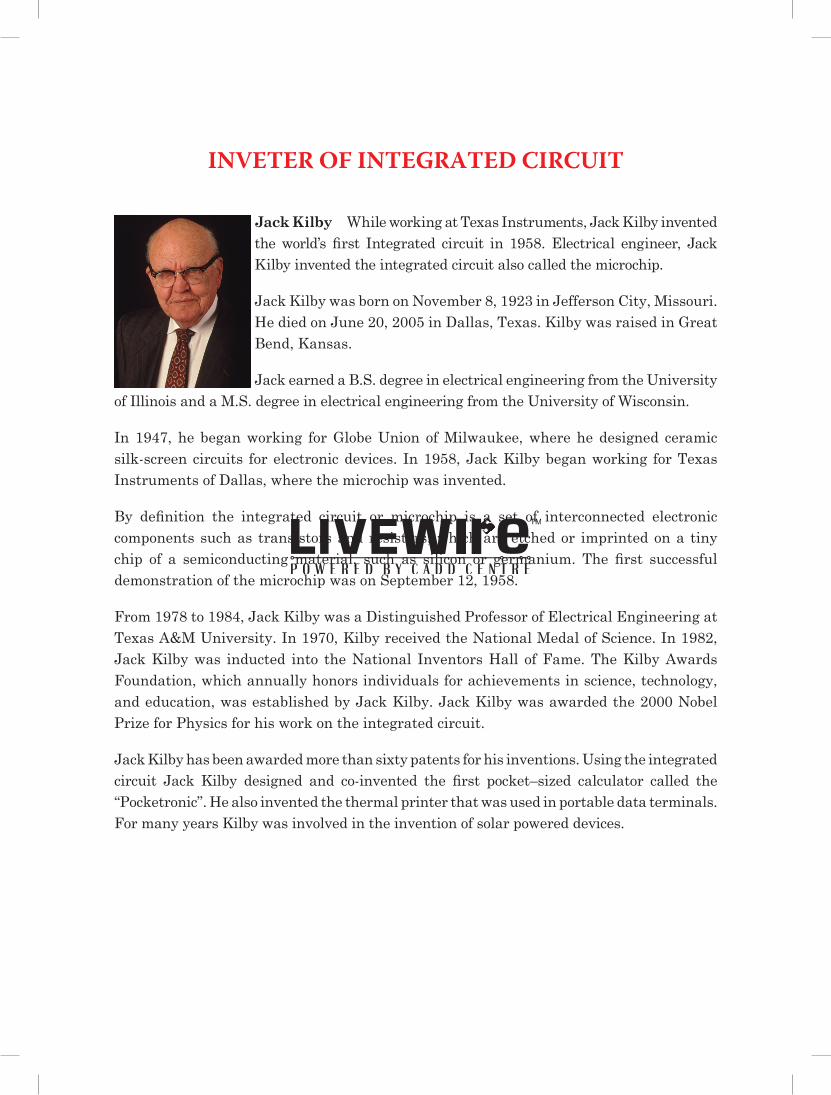
INVETER OF INTEGRATED CIRCUIT
Jack Kilby While working at Texas Instruments, Jack Kilby invented the world’s first Integrated circuit in 1958. Electrical engineer, Jack Kilby invented the integrated circuit also called the microchip.
Jack Kilby was born on November 8, 1923 in Jefferson City, Missouri. He died on June 20, 2005 in Dallas, Texas. Kilby was raised in Great Bend, Kansas.
Jack earned a B.S. degree in electrical engineering from the University of Illinois and a M.S. degree in electrical engineering from the University of Wisconsin.
In 1947, he began working for Globe Union of Milwaukee, where he designed ceramic silk-screen circuits for electronic devices. In 1958, Jack Kilby began working for Texas Instruments of Dallas, where the microchip was invented.
By definition the integrated circuit or microchip is a set of interconnected electronic components such as transistors and resistors, which are etched or imprinted on a tiny chip of a semiconducting material, such as silicon or germanium. The first successful demonstration of the microchip was on September 12, 1958.
From 1978 to 1984, Jack Kilby was a Distinguished Professor of Electrical Engineering at Texas A&M University. In 1970, Kilby received the National Medal of Science. In 1982, Jack Kilby was inducted into the National Inventors Hall of Fame. The Kilby Awards Foundation, which annually honors individuals for achievements in science, technology, and education, was established by Jack Kilby. Jack Kilby was awarded the 2000 Nobel Prize for Physics for his work on the integrated circuit.
Jack Kilby has been awarded more than sixty patents for his inventions. Using the integrated circuit Jack Kilby designed and co-invented the first pocket–sized calculator called the “Pocketronic”. He also invented the thermal printer that was used in portable data terminals. For many years Kilby was involved in the invention of solar powered devices.

Disclaimer
This Reference Guide is intended solely for the use of individual who has registered for a course at CADD Centre. This
guide covers most of the prescribed industry specific curriculum. You are welcome to refer other manuals and books to
gain wider knowledge on the subject. This guide contains additional portions and topics for your self-learning after gaining
required expertise on the curriculum covered during the instructor led training by CADD Centre.
Do not assume that all the topics included in the book will be covered during the instructor led training program at
CADD Centre as it is a reference guide meant for your use even after the course with us. This Reference Guide is a
life time ready reference material for the respective application too. Changes may be made and enforced time to time
at company’s discretion.
For feedback/suggestion on the contents of this material please write to [email protected]
C O N T E N T S vii
ContentsCHAPTER 1
VERILOG HDL DESIGN AND VLSI DESIGN FLOW .................................................................. 3
1.1 Overview of a Design using Verilog HDL ................................................................................................................ 4
1.2 Verilog Hardware Description Language ................................................................................................................... 5
1.3 System Representation ................................................................................................................................................... 7
1.4 Data Types & Nets ......................................................................................................................................................... 8
1.5 Strength Levels & Contention ...................................................................................................................................... 9
CHAPTER 2
GATE LEVEL MODELING ............................................................................................................. 17
2.1 Introduction to Gate Level Modeling ......................................................................................................................18
2.2 Design and Simulation of Full adder .......................................................................................................................23
2.3 Test bench .......................................................................................................................................................................25
2.4 Example for a testbench ..............................................................................................................................................28
CHAPTER 3
ELABORATION & SIMULATION METHODOLOGY OF DESIGN ....................................... 33
3.1 Elaboration of Full adder ...........................................................................................................................................34
3.2 Simulation of a Full adder ..........................................................................................................................................35
3.3 Alternate way of Simulation–1 .................................................................................................................................36
3.4 Frequently used options ..............................................................................................................................................41
3.5 Alternate way of Simulation–2 .................................................................................................................................42
3.6 Design of 4:1 Multiplexer ..........................................................................................................................................46
3.7 Schematic Tracer window ............................................................................................................................................48
3.8 User Defined Primitives ..............................................................................................................................................49
C O N T E N T Sviii
CHAPTER 4
DATAFLOW MODELING .............................................................................................................. 57
4.1 Introduction to Dataflow Modeling.........................................................................................................................58
4.2 Continuous Assignment ..............................................................................................................................................58
4.3 Implicit Continuous Assignment ..............................................................................................................................59
4.4 Delays ..............................................................................................................................................................................60
4.5 Operators and Operands .............................................................................................................................................61
4.6 Designing an Octal–to–Binary Encoder ..................................................................................................................74
4.7 Design of 4:1 Multiplexer ..........................................................................................................................................76
CHAPTER 5
BEHAVIORAL MODELING ........................................................................................................... 81
5.1 Introduction to Behavioral Modeling .......................................................................................................................82
5.2 Structured Procedures ..................................................................................................................................................82
5.3 Procedural Assignments ..............................................................................................................................................85
5.4 Race around condition ................................................................................................................................................88
5.5 Timing Controls ............................................................................................................................................................89
5.6 Event–Based Timing Control .....................................................................................................................................93
5.7 Conditional Statements ...............................................................................................................................................96
5.8 Loop Statements ...........................................................................................................................................................99
5.9 Procedural Continuous Assignment ...................................................................................................................... 103
5.10 Sequential and Parallel Blocks .............................................................................................................................. 106
5.11 Tasks & Functions ................................................................................................................................................... 108
5.12 Compiler Directives ................................................................................................................................................ 114
SELF ASSESSMENT ......................................................................................................................123
WORK BOOK .................................................................................................................................127
VERILOG HDL DESIGN AND VLSI
DESIGN FLOW1

VERILOG HDL DESIGN AND VLSI DESIGN FLOW
INTRODUCTION
In this chapter, we come to learn about VLSI (Very Large
Scale Integration) design flow, which relates to representing
a model right from its specification to the physical design
itself. Also, the different approaches in the VLSI methodology
is briefed. Features and attributes of HDL Verilog comprise
another essential part in this chapter, including definitions
for modules, ports and nets.
VLSI System design using IES–XL Simulatorchapter14
1.1 Overview of a Design using Verilog HDLSeveral aspects go into a hardware while designing it. To gain knowledge over its design process, complete information regarding both the behavioural and structural aspects of the hardware are required. In that information, however, our focus might rest on a particular aspect of interest. This is called abstraction in designing.
The hardware description language Verilog has been developed to provide a means of describing, validating, maintaining and exchanging design information on complex digital VLSI chips across several levels of design abstractions used in the design process.
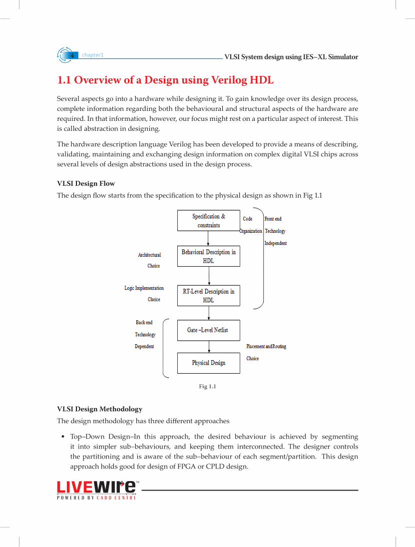
VLSI Design FlowThe design flow starts from the specification to the physical design as shown in Fig 1.1
Fig 1.1
VLSI Design MethodologyThe design methodology has three different approaches
• Top–Down Design–In this approach, the desired behaviour is achieved by segmenting it into simpler sub–behaviours, and keeping them interconnected. The designer controls the partitioning and is aware of the sub–behaviour of each segment/partition. This design approach holds good for design of FPGA or CPLD design.

VLSI System design using IES–XL Simulator chapter1 5
• Bottom–up Design the desired behavior is realized by interconnecting available component parts. This design approach holds good for ASIC design
• Mixed top–down and bottom–up methodology–It is a blend of both the top–down and bottom–up methodology. This design approach holds good for reuse of the component in various designs.
1.2 Verilog Hardware Description LanguageVerilog was started initially as a proprietary hardware modeling language by Gateway Design Automation Inc. around 1984. It is rumored that the original language was designed by borrowing features from the most popular HDL language of the time, called HiLo, as well as from traditional computer languages such as C. Verilog simulator was first used in 1985 and was extended substantially through 1987. Verilog–XL, a new version of simulator with the enhanced language and simulator was introduced in 1985. It gained a strong foothold among the high–end designers for the following reasons:
• Behavioral construct models of Verilog could be described as both hardware and test stimulus
• Verilog–XL simulator was fast, especially at the gate level and could handle designs in excess–of more than 100,000 gates.
• In 1990, Cadence decided to open the language to the public, and thus OVI (Open Verilog International) was formed.
• In 1993, an IEEE working group was established under the Design Automation Sub–Committee to produce the IEEE Verilog 1364.
• In December 1995, the final draft of Verilog was approved and the result is known as IEEE Std. 1364–1995.IEEE 1364–2005 is the latest Verilog HDL standard.
Importance of HDLs• Designs can be described at a very abstract level by use of HDLs. Designers can write their
RTL description without choosing a specific fabrication technology.
• By designing through HDLs, functional verification of the design can be done early in the design cycle itself.
• Designing with HDL is analogous to the computer programming.
VLSI System design using IES–XL Simulatorchapter16
Features of VerilogVerilog is a universal concept. It allows the entire design process to be performed within a single design environment.
• Industrial support–Verilog supports switch level modeling, hence has always been popular with ASIC designers, as it allows fast simulation and effective synthesis.
• Extensibility–The IEEE standard 1364 contains definition of PLI (Programming Language interface) that allows for extension of Verilog capabilities.
• Similarity with C–Similar syntax to the C programming language.
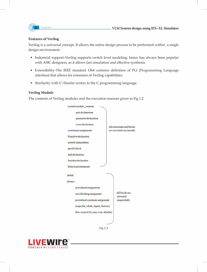
Verilog ModuleThe contents of Verilog modules and the execution manner given in Fig 1.2
Fig 1.2
VLSI System design using IES–XL Simulator chapter1 7
1.3 System Representation
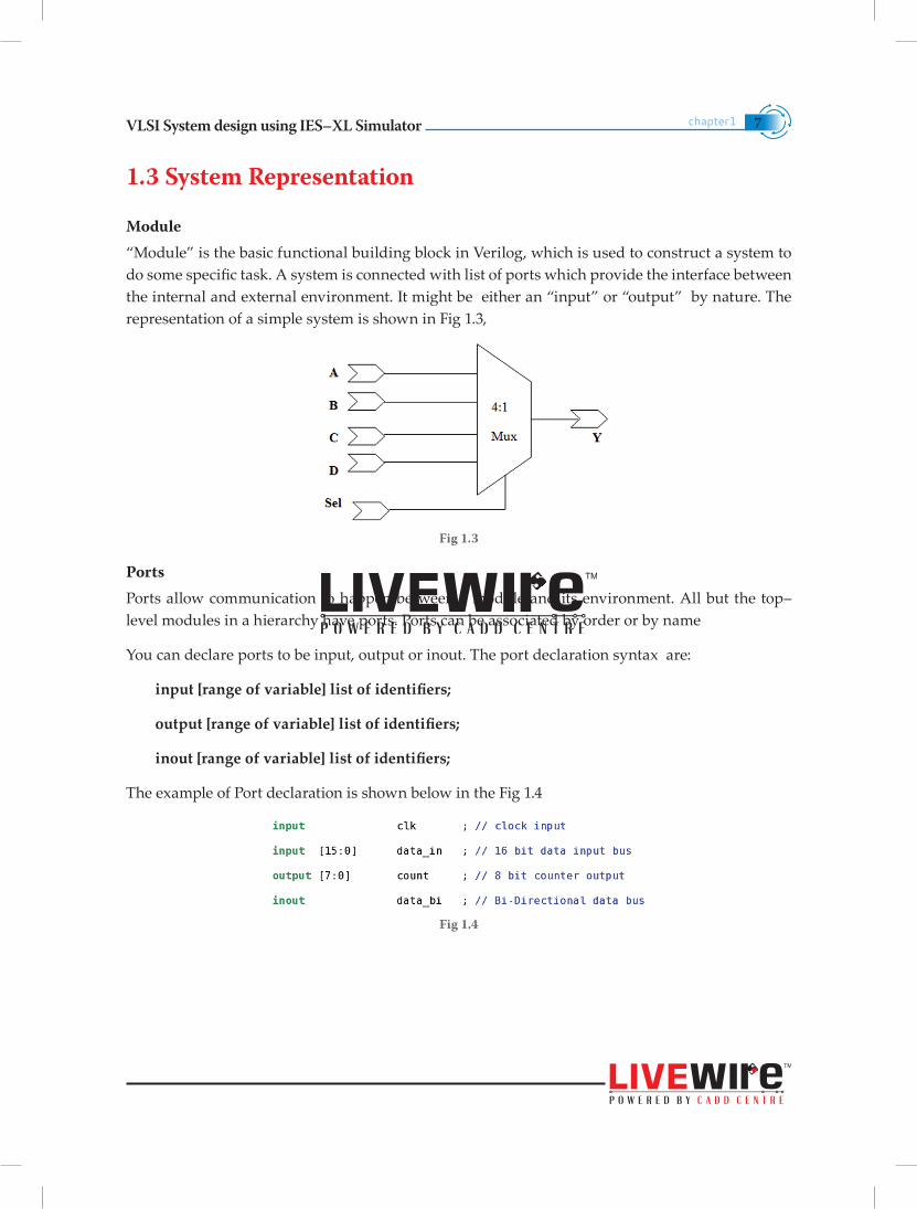
Module“Module” is the basic functional building block in Verilog, which is used to construct a system to do some specific task. A system is connected with list of ports which provide the interface between the internal and external environment. It might be either an “input” or “output” by nature. The representation of a simple system is shown in Fig 1.3,
Fig 1.3
PortsPorts allow communication to happen between a module and its environment. All but the top–level modules in a hierarchy have ports. Ports can be associated by order or by name
You can declare ports to be input, output or inout. The port declaration syntax are:
input [range of variable] list of identifiers;
output [range of variable] list of identifiers;
inout [range of variable] list of identifiers;
The example of Port declaration is shown below in the Fig 1.4
Fig 1.4
VLSI System design using IES–XL Simulatorchapter18
Port Connection RulesInternally, the inputs must always be of type net, whereas externally, the inputs can be connected to a variable of type “reg” or “net”.
Outputs, internally can be of type “net” or “reg”, whereas externally, the outputs must be connected to a variable of type net.
Inouts, whether internally or externally, must always be type “net”, can only be connected to a variable net type. The representation of port connection is shown in Fig 1.5
Fig 1.5
NoteIt is legal to connect the internal and external ports even though they are of different sizes. But sometimes the synthesis tool could report problems relating to the connection.
Unconnected ports are allowed by using a “,”
A net data type is required if a signal can be driven to a structural connection.
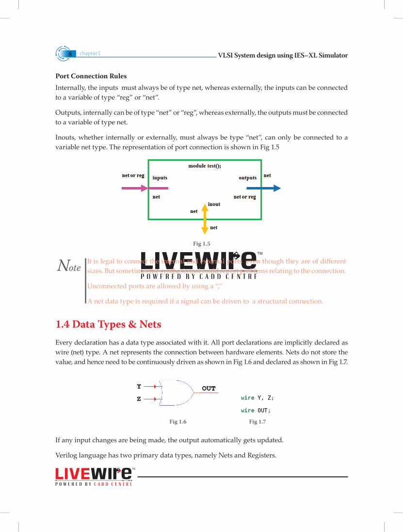
1.4 Data Types & NetsEvery declaration has a data type associated with it. All port declarations are implicitly declared as wire (net) type. A net represents the connection between hardware elements. Nets do not store the value, and hence need to be continuously driven as shown in Fig 1.6 and declared as shown in Fig 1.7.
Fig 1.6 Fig 1.7
If any input changes are being made, the output automatically gets updated.
Verilog language has two primary data types, namely Nets and Registers.

VLSI System design using IES–XL Simulator chapter1 9
Nets: They Represent the structural connection between the components.
Registers: They Represent variables required to store data.
Types of NetsTo model the functionality of net for different kind of hardware’s, we might go with different types of Nets which are given in Fig 1.8.
Fig 1.8
1.5 Strength Levels & ContentionVerilog allows signals to have both logic values and strength values. It holds the logic values as 0,1, X and Z. Strength values are generally used to resolve combinations of multiple signals and represent the behavior of actual hardware elements as accurately as possible.
Driving strengths are used for signal values that are driven on a net. Storage strengths are used to model charge storage in “trireg” type nets.
In case of signal contention, its value is resolved using logic strengths.
The Strength Level for logic 1 is given in Fig 1.9.,
Fig 1.9
VLSI System design using IES–XL Simulatorchapter110
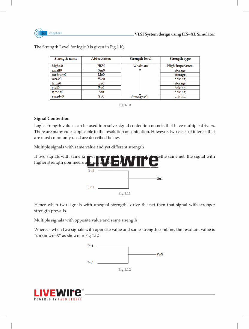
The Strength Level for logic 0 is given in Fig 1.10,
Fig 1.10
Signal ContentionLogic strength values can be used to resolve signal contention on nets that have multiple drivers. There are many rules applicable to the resolution of contention. However, two cases of interest that are most commonly used are described below,
Multiple signals with same value and yet different strength
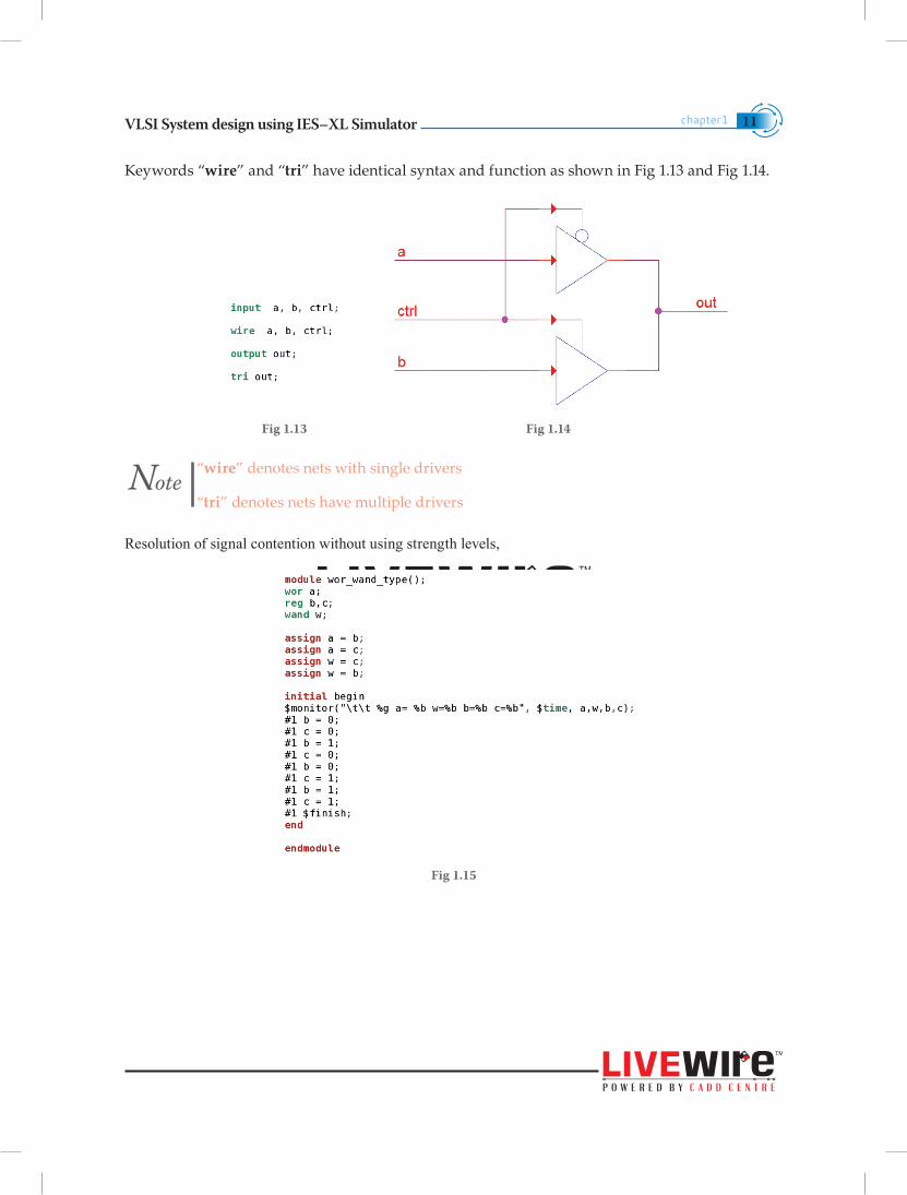
If two signals with same known value and different strength drive the same net, the signal with higher strength domineers as shown in Fig 1.11
Fig 1.11
Hence when two signals with unequal strengths drive the net then that signal with stronger strength prevails.
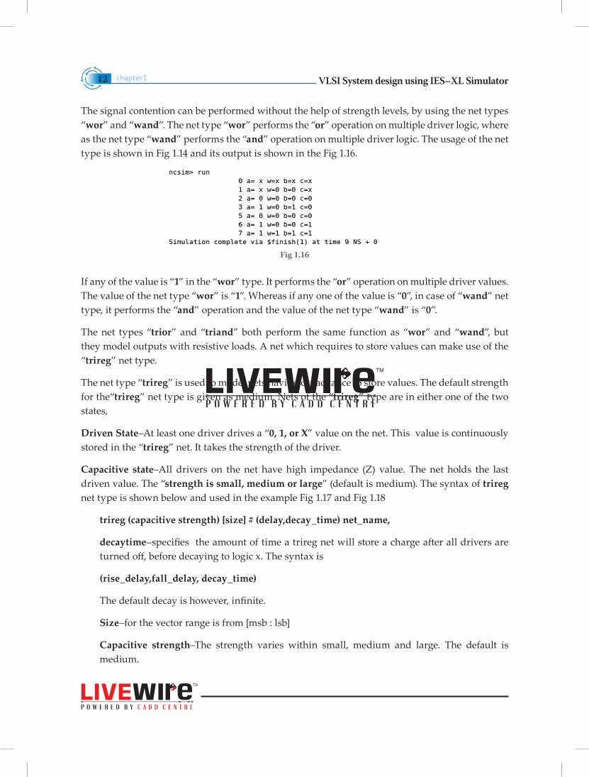
Multiple signals with opposite value and same strength
Whereas when two signals with opposite value and same strength combine, the resultant value is “unknown–X” as shown in Fig 1.12
Fig 1.12
VLSI System design using IES–XL Simulator chapter1 11
Keywords “wire” and “tri” have identical syntax and function as shown in Fig 1.13 and Fig 1.14.
Fig 1.13 Fig 1.14
Note“wire” denotes nets with single drivers
“tri” denotes nets have multiple drivers
Resolution of signal contention without using strength levels,
Fig 1.15
VLSI System design using IES–XL Simulatorchapter112
The signal contention can be performed without the help of strength levels, by using the net types “wor” and “wand”. The net type “wor” performs the “or” operation on multiple driver logic, where as the net type “wand” performs the “and” operation on multiple driver logic. The usage of the net type is shown in Fig 1.14 and its output is shown in the Fig 1.16.
Fig 1.16
If any of the value is “1” in the “wor” type. It performs the “or” operation on multiple driver values. The value of the net type “wor” is “1”. Whereas if any one of the value is “0”, in case of “wand” net type, it performs the “and” operation and the value of the net type “wand” is “0”.
The net types “trior” and “triand” both perform the same function as “wor” and “wand”, but they model outputs with resistive loads. A net which requires to store values can make use of the “trireg” net type.
The net type “trireg” is used to model nets having capacitance to store values. The default strength for the“trireg” net type is given as medium. Nets of the “trireg” type are in either one of the two states,
Driven State–At least one driver drives a “0, 1, or X” value on the net. This value is continuously stored in the “trireg” net. It takes the strength of the driver.
Capacitive state–All drivers on the net have high impedance (Z) value. The net holds the last driven value. The “strength is small, medium or large” (default is medium). The syntax of trireg net type is shown below and used in the example Fig 1.17 and Fig 1.18
trireg (capacitive strength) [size] # (delay,decay_time) net_name,
decaytime–specifies the amount of time a trireg net will store a charge after all drivers are turned off, before decaying to logic x. The syntax is
(rise_delay,fall_delay, decay_time)
The default decay is however, infinite.
Size–for the vector range is from [msb : lsb]
Capacitive strength–The strength varies within small, medium and large. The default is medium.
VLSI System design using IES–XL Simulator chapter1 13
This chapter explains
• An Overview of Digital Design with Verilog HDL. VLSI Design flow and design methodology using hierarchical Modeling concepts.
• Identifying the components of a Verilog module definition such as module contents and understanding how to define the port list for a module and declare it in Verilog.
• Defining the logic value set and data types.
• Learning the strength level of the signals and signal contention.
The usage of trireg net type to module the logic contention is shown below in the Fig 1.17 and Fig 1.18
Fig 1.17 Fig 1.18
Highlights
VLSI System design using IES–XL Simulatorchapter114
1. What do you mean by module? What are the basic components of a module?
2. Define module with the module name “test_module” consisting of 4 user defined input ports, 2 user defined output ports and 1 input/output ports of 4–bit variables.
3. Declare 4 net with user defined names, the first net should be of 1–bit value, the second net should be of 3–bit value, the third & fourth net should be of 4–bit fixed value to logic value “1010” and “0101”.
4. Declare a variable reset that can hold its value of 1–bit value and after 100 time unit reset should be de–asserted.
5. Define a scalar net variable of 1–bit value and two vectors net of 5–bit value. Do the same the register variables.
6. What are the port connection rules?
7. Why the ports of type “input” and “inout” cannot be declared as “reg” datatype?
8. What do you mean by signal contention?
Questions
GATE LEVEL MODELING 2

GATE LEVEL MODELING
INTRODUCTION
Gate level modeling, is the most simplest version of modeling,
which can be used by designers who are beginners with
minimal knowledge of digital circuit designing. The various
aspects of gate level modeling, including the gate & switch
delays and testbench with appropriate examples are discussed
in this chapter. A design and simulation methodology of a
full adder, and also a case application of test bench on a full
adder is descriptively explained in this chapter.
VLSI System design using IES–XL Simulatorchapter118
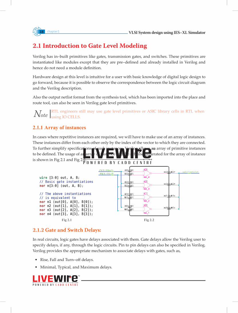
2.1 Introduction to Gate Level ModelingVerilog has in–built primitives like gates, transmission gates, and switches. These primitives are instantiated like modules except that they are pre–defined and already installed in Verilog and hence do not need a module definition.
Hardware design at this level is intuitive for a user with basic knowledge of digital logic design to go forward, because it is possible to observe the correspondence between the logic circuit diagram and the Verilog description.
Also the output netlist format from the synthesis tool, which has been imported into the place and route tool, can also be seen in Verilog gate level primitives.
NoteRTL engineers still may use gate level primitives or ASIC library cells in RTL when using IO CELLS.
2.1.1 Array of instances
In cases where repetitive instances are required, we will have to make use of an array of instances. These instances differ from each other only by the index of the vector to which they are connected. To further simplify specifications of such instances, Verilog allows an array of primitive instances to be defined. The usage of an array of instance and the scheme generated for the array of instance is shown in Fig 2.1 and Fig 2.2.
Fig 2.1 Fig 2.2
2.1.2 Gate and Switch Delays:
In real circuits, logic gates have delays associated with them. Gate delays allow the Verilog user to specify delays, if any, through the logic circuits. Pin to pin delays can also be specified in Verilog. Verilog provides the appropriate mechanism to associate delays with gates, such as,
• Rise, Fall and Turn–off delays.
• Minimal, Typical, and Maximum delays.
VLSI System design using IES–XL Simulator chapter1 19
In Verilog, delays can be denoted with the symbol #’num’ as shown in the examples below, where # is a special character to indicate a delay, and ‘num’ is the number of ticks a simulator is supposed to delay the current statement execution.
#10 A = B : Delay by 10, i.e. execute after 10 unit of time,
#20 xor (Out, X, Y) : Delay by 20 units of time assigned to “Out”.
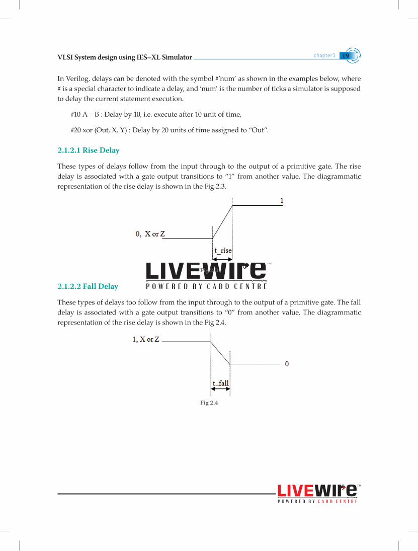
2.1.2.1 Rise Delay
These types of delays follow from the input through to the output of a primitive gate. The rise delay is associated with a gate output transitions to “1” from another value. The diagrammatic representation of the rise delay is shown in the Fig 2.3.
Fig 2.3
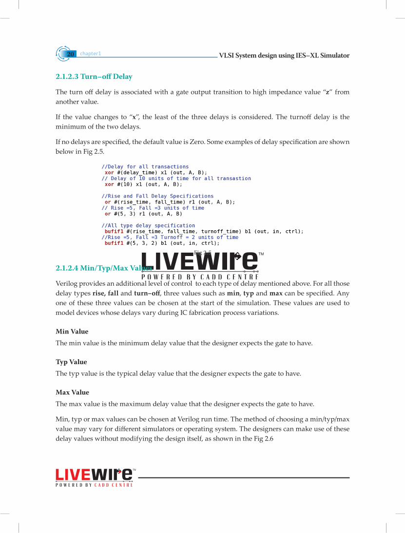
2.1.2.2 Fall Delay
These types of delays too follow from the input through to the output of a primitive gate. The fall delay is associated with a gate output transitions to “0” from another value. The diagrammatic representation of the rise delay is shown in the Fig 2.4.
Fig 2.4
VLSI System design using IES–XL Simulatorchapter120
2.1.2.3 Turn–off Delay
The turn off delay is associated with a gate output transition to high impedance value “z” from another value.
If the value changes to “x”, the least of the three delays is considered. The turnoff delay is the minimum of the two delays.
If no delays are specified, the default value is Zero. Some examples of delay specification are shown below in Fig 2.5.
Fig 2.5
2.1.2.4 Min/Typ/Max Values
Verilog provides an additional level of control to each type of delay mentioned above. For all those delay types rise, fall and turn–off, three values such as min, typ and max can be specified. Any one of these three values can be chosen at the start of the simulation. These values are used to model devices whose delays vary during IC fabrication process variations.
Min ValueThe min value is the minimum delay value that the designer expects the gate to have.
Typ ValueThe typ value is the typical delay value that the designer expects the gate to have.
Max ValueThe max value is the maximum delay value that the designer expects the gate to have.
Min, typ or max values can be chosen at Verilog run time. The method of choosing a min/typ/max value may vary for different simulators or operating system. The designers can make use of these delay values without modifying the design itself, as shown in the Fig 2.6
VLSI System design using IES–XL Simulator chapter1 21
Fig 2.6
2.1.2.5 Examples for Gate Delays
Let us consider a simple example to illustrate the use of gate delays to model the timing in logic circuits. In this example we will compile, elaborate and simulate the gate delays. The HDL for Gate delays have been listed below in the Fig 2.7,
Fig 2.7
VLSI System design using IES–XL Simulatorchapter122
After creating the design using HDL, cross check whether the design meets the specifications listed by you as it is being designed. Compile the Verilog design units with the ncvlog compiler, Which does performs,
• Checks on the syntax and semantics
• Generates Design Data
• Produces ncvlog.log log file.
The compilation of the delay example is shown in the Fig 2.8,
Fig 2.8
To construct the design hierarchy and to connect the signals, elaborate your design with ncelab command as shown in the Fig 2.9.
Fig 2.9
VLSI System design using IES–XL Simulator chapter1 23
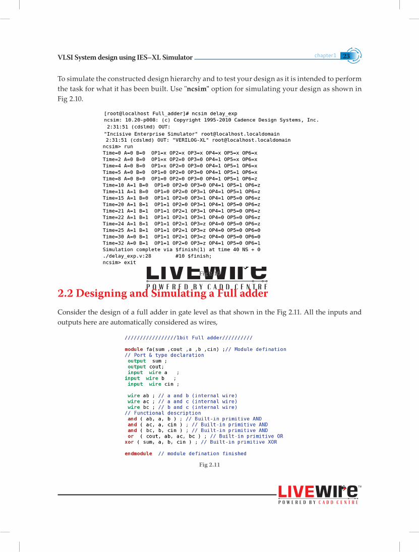
To simulate the constructed design hierarchy and to test your design as it is intended to perform the task for what it has been built. Use "ncsim" option for simulating your design as shown in Fig 2.10.
Fig 2.10
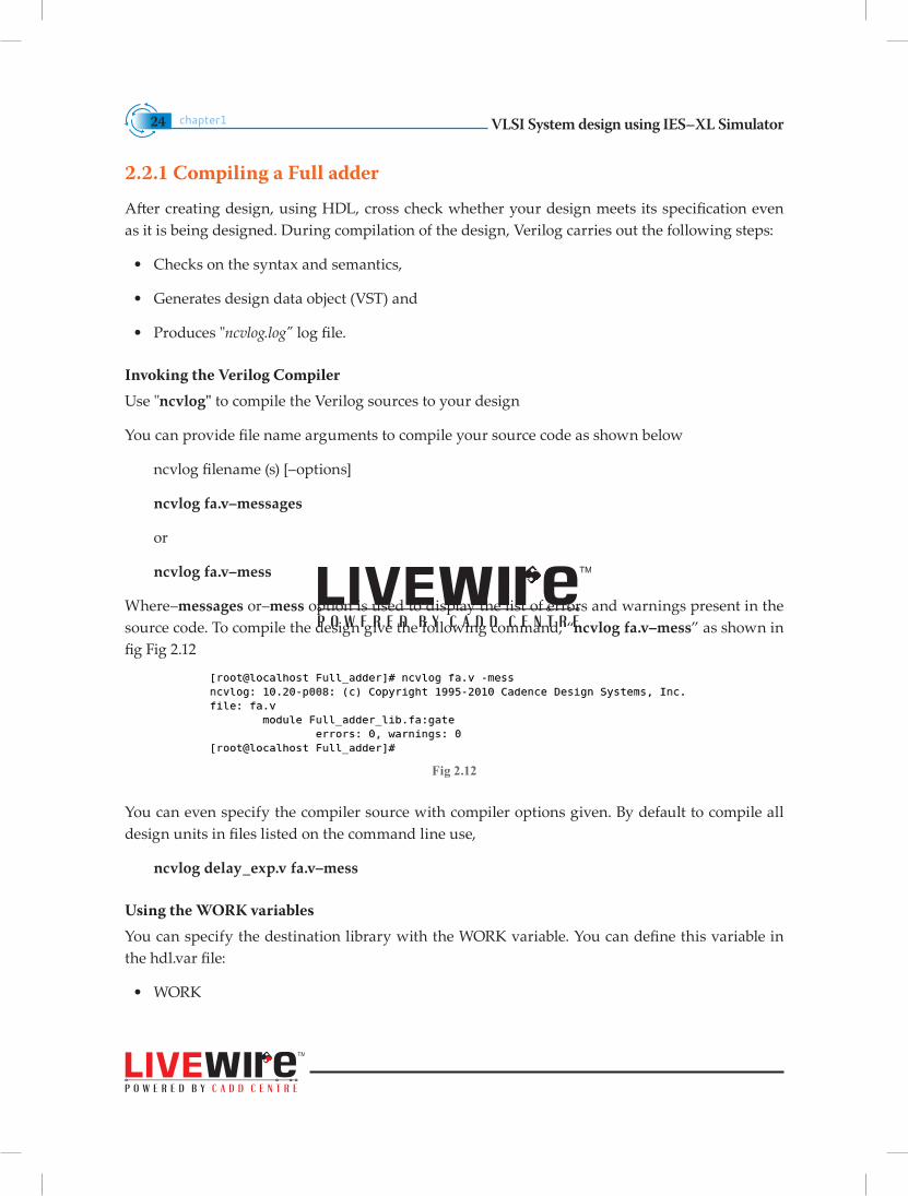
2.2 Designing and Simulating a Full adderConsider the design of a full adder in gate level as that shown in the Fig 2.11. All the inputs and outputs here are automatically considered as wires,
Fig 2.11
VLSI System design using IES–XL Simulatorchapter124
2.2.1 Compiling a Full adder
After creating design, using HDL, cross check whether your design meets its specification even as it is being designed. During compilation of the design, Verilog carries out the following steps:
• Checks on the syntax and semantics,
• Generates design data object (VST) and
• Produces "ncvlog.log" log file.
Invoking the Verilog CompilerUse "ncvlog" to compile the Verilog sources to your design
You can provide file name arguments to compile your source code as shown below
ncvlog filename (s) [–options]
ncvlog fa.v–messages
or
ncvlog fa.v–mess
Where–messages or–mess option is used to display the list of errors and warnings present in the source code. To compile the design give the following command, “ncvlog fa.v–mess” as shown in fig Fig 2.12
Fig 2.12
You can even specify the compiler source with compiler options given. By default to compile all design units in files listed on the command line use,
ncvlog delay_exp.v fa.v–mess
Using the WORK variablesYou can specify the destination library with the WORK variable. You can define this variable in the hdl.var file:
• WORK
VLSI System design using IES–XL Simulator chapter1 25
It suggests a suitable library in which to store the compiled objects. This variable overrides the LIB_MAP variable
Define WORK worklib
2.3 Test benchThe functionality of the design block can be tested by applying stimulus and checking the results. Such a block is called the stimulus block. This stimulus block is also commonly called a test bench. Test benches help you verify the correctness of a design. A test bench is a top level module without inputs and outputs. Two styles of stimulus application are possible with it.
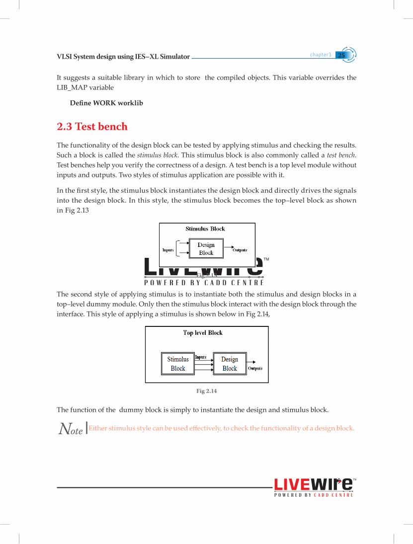
In the first style, the stimulus block instantiates the design block and directly drives the signals into the design block. In this style, the stimulus block becomes the top–level block as shown in Fig 2.13
Fig 2.13
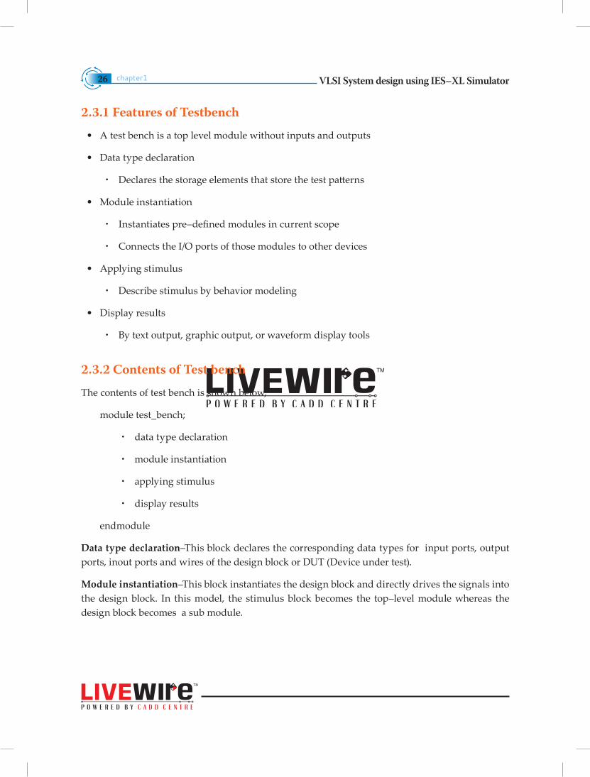
The second style of applying stimulus is to instantiate both the stimulus and design blocks in a top–level dummy module. Only then the stimulus block interact with the design block through the interface. This style of applying a stimulus is shown below in Fig 2.14,
Fig 2.14
The function of the dummy block is simply to instantiate the design and stimulus block.
Note Either stimulus style can be used effectively, to check the functionality of a design block.
VLSI System design using IES–XL Simulatorchapter126
2.3.1 Features of Testbench
• A test bench is a top level module without inputs and outputs
• Data type declaration
x Declares the storage elements that store the test patterns
• Module instantiation
x Instantiates pre–defined modules in current scope
x Connects the I/O ports of those modules to other devices
• Applying stimulus
x Describe stimulus by behavior modeling
• Display results
x By text output, graphic output, or waveform display tools
2.3.2 Contents of Test bench
The contents of test bench is shown below,
module test_bench;
x data type declaration
x module instantiation
x applying stimulus
x display results
endmodule
Data type declaration–This block declares the corresponding data types for input ports, output ports, inout ports and wires of the design block or DUT (Device under test).
Module instantiation–This block instantiates the design block and directly drives the signals into the design block. In this model, the stimulus block becomes the top–level module whereas the design block becomes a sub module.

VLSI System design using IES–XL Simulator chapter1 27
Applying stimulus–This block declares the stimulus for the input ports present within the design block or DUT.
Display results–This block displays and monitors the result of a design block or DUT. Verilog provides a standard set of system tasks for certain routine operations. All the system tasks appear in the form of $<keyword>. Some of the frequently used system tasks are listed below,
$display–It is the main system task for displaying values of variables or strings or expressions. Usage of display system task is shown below,
$display (d1,d2,d3…..dn);Where d1,d2,d3….dn can be quoted if strings or variables or expressions are used.
$monitor–This system task provides a mechanism to monitor a signal when its value changes. Usage of a monitor system task is shown below,
$monitor (d1,d2,d3…..dn);Where the parameters d1,d2,d3….dn can be variables, signal names or quoted strings. This system task continuously monitors the values of the variables or signals specified in the parameter list.
$time–This system task monitors the change of signal values according to the delay value assigned to the variables.
$stop–This task is used whenever the designer wants to suspend the simulation and examine the values of signals in the design. This task puts the simulation in an interactive mode. The designer can then debug the design from staying in the interactive mode.
$finish–This task terminates the simulation forcibly.
VLSI System design using IES–XL Simulatorchapter128
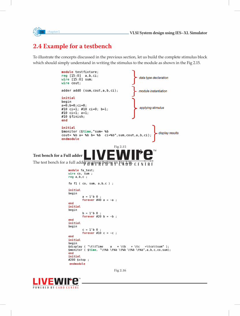
2.4 Example for a testbenchTo illustrate the concepts discussed in the previous section, let us build the complete stimulus block which should simply understand in writing the stimulus to the module as shown in the Fig 2.15.
Fig 2.15
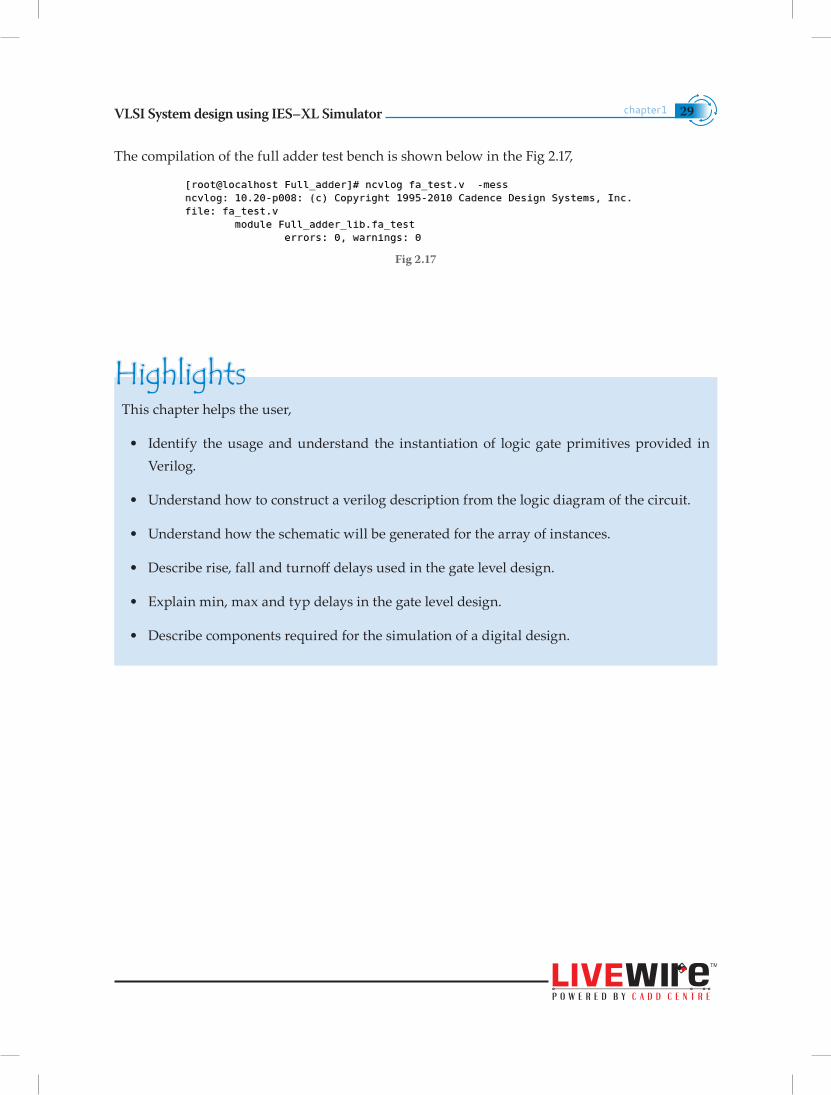
Test bench for a Full adderThe test bench for a full adder is given below in Fig 2.16,
Fig 2.16
VLSI System design using IES–XL Simulator chapter1 29
This chapter helps the user,
• Identify the usage and understand the instantiation of logic gate primitives provided in Verilog.
• Understand how to construct a verilog description from the logic diagram of the circuit.
• Understand how the schematic will be generated for the array of instances.
• Describe rise, fall and turnoff delays used in the gate level design.
• Explain min, max and typ delays in the gate level design.
• Describe components required for the simulation of a digital design.
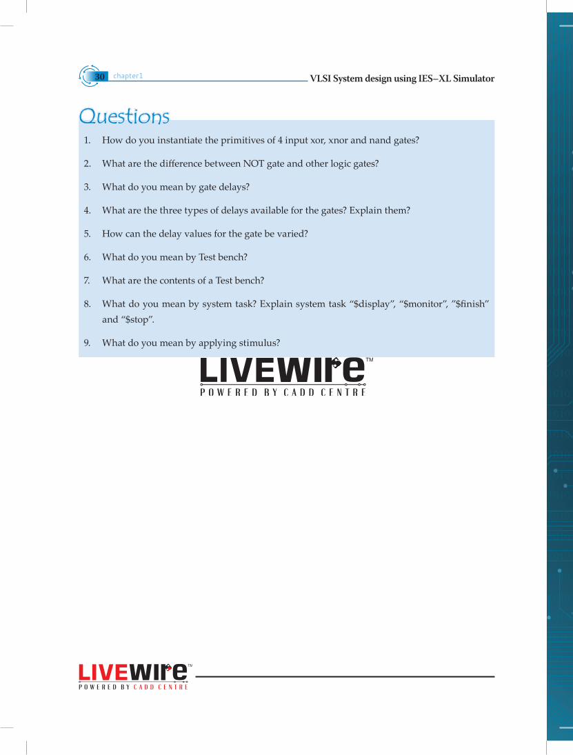
The compilation of the full adder test bench is shown below in the Fig 2.17,
Fig 2.17
Highlights
VLSI System design using IES–XL Simulatorchapter130
1. How do you instantiate the primitives of 4 input xor, xnor and nand gates?
2. What are the difference between NOT gate and other logic gates?
3. What do you mean by gate delays?
4. What are the three types of delays available for the gates? Explain them?
5. How can the delay values for the gate be varied?
6. What do you mean by Test bench?
7. What are the contents of a Test bench?
8. What do you mean by system task? Explain system task “$display”, “$monitor”, ”$finish” and “$stop”.
9. What do you mean by applying stimulus?
Questions
ELABORATION & SIMULATION
METHODOLOGY OF DESIGN
3

ELABORATION & SIMULATION METHODOLOGY OF DESIGN
INTRODUCTION
This chapter predominantly deals with the elaboration and simulation
facilities available with Verilog. These facilities work on ensuring
the correctness of a design. Full adder compilations, simulations and
elaborations are done in detail for understanding. Also features of Verilog
such as Multiplexer, that strives to achieve an output from multiple inputs
and user defined primitives are described.
VLSI System design using IES–XL Simulatorchapter 334
3.1 Elaboration of Full adderThe Elaboration facility specifies the top level design units that are to be elaborated, the design configuration, the destination snapshot name and maximize subsequent simulator performance. The elaboration facility of your compiled Verilog design performs the following operations:
• Constructs design hierarchy and connect signals
• Creates signature object (SIG) and code object (COD),
• Creates initial simulation snapshot object (SSS)
• Produces “ncelab.log” log file.
3.1.1 Invoking the Elaborator
The design can be elaborated using “ncelab”. The argument can be either a compiled Verilog configuration or at least one compiled top level design unit.
You can provide file name arguments to elaborate upon your source code as shown below
ncelab filename (without extension) [–options]
ncelab fa_test–access +wc–status
or
ncelab fa_test –message
or
ncelab fa_test –mess
Where–messages or–mess option is used to display the list of design hierarchy summary present in the source code.
VLSI System design using IES–XL Simulator chapter 3 35
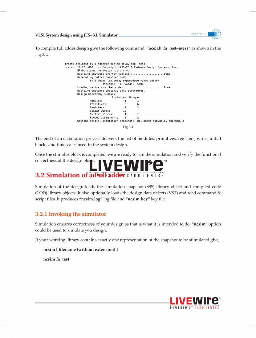
To compile full adder design give the following command, “ncelab fa_test–mess” as shown in the Fig 3.1,
Fig 3.1
The end of an elaboration process delivers the list of modules, primitives, registers, wires, initial blocks and timescales used in the system design.
Once the stimulus block is completed, we are ready to run the simulation and verify the functional correctness of the design block.
3.2 Simulation of a Full adderSimulation of the design loads the simulation snapshot (SSS) library object and compiled code (COD) library objects. It also optionally loads the design data objects (VST) and read command & script files. It produces “ncsim.log” log file and “ncsim.key” key file.
3.2.1 Invoking the simulator
Simulation ensures correctness of your design as that is what it is intended to do. “ncsim” option could be used to simulate you design.
If your working library contains exactly one representation of the snapshot to be stimulated give,
ncsim [ filename (without extension) ]
ncsim fa_test
VLSI System design using IES–XL Simulatorchapter 336
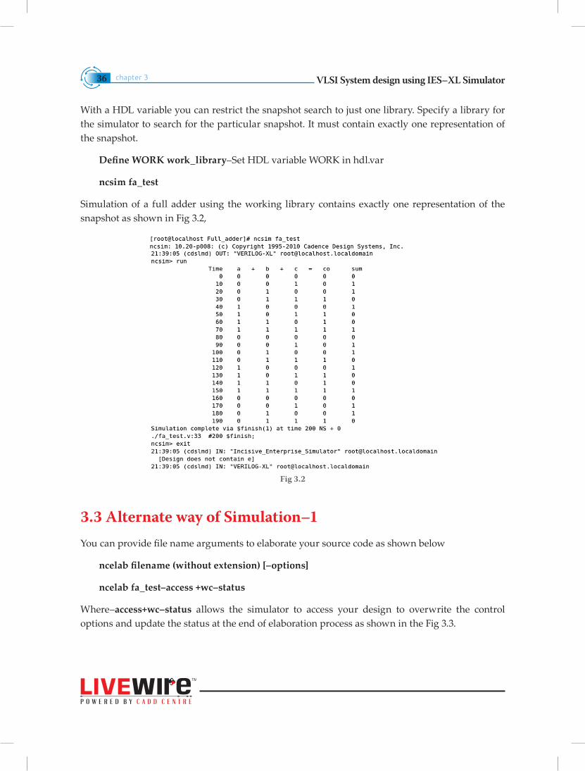
With a HDL variable you can restrict the snapshot search to just one library. Specify a library for the simulator to search for the particular snapshot. It must contain exactly one representation of the snapshot.
Define WORK work_library–Set HDL variable WORK in hdl.var
ncsim fa_test
Simulation of a full adder using the working library contains exactly one representation of the snapshot as shown in Fig 3.2,
Fig 3.2
3.3 Alternate way of Simulation–1You can provide file name arguments to elaborate your source code as shown below
ncelab filename (without extension) [–options]
ncelab fa_test–access +wc–status
Where–access+wc–status allows the simulator to access your design to overwrite the control options and update the status at the end of elaboration process as shown in the Fig 3.3.
VLSI System design using IES–XL Simulator chapter 3 37
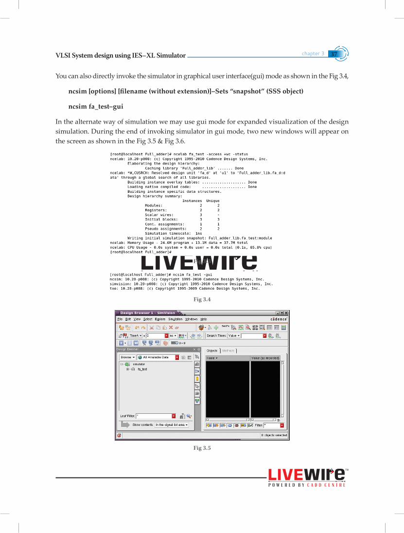
You can also directly invoke the simulator in graphical user interface(gui) mode as shown in the Fig 3.4,
ncsim [options] [filename (without extension)]–Sets “snapshot” (SSS object)
ncsim fa_test–gui
In the alternate way of simulation we may use gui mode for expanded visualization of the design simulation. During the end of invoking simulator in gui mode, two new windows will appear on the screen as shown in the Fig 3.5 & Fig 3.6.
Fig 3.3
Fig 3.4
Fig 3.5
VLSI System design using IES–XL Simulatorchapter 338
Fig 3.6
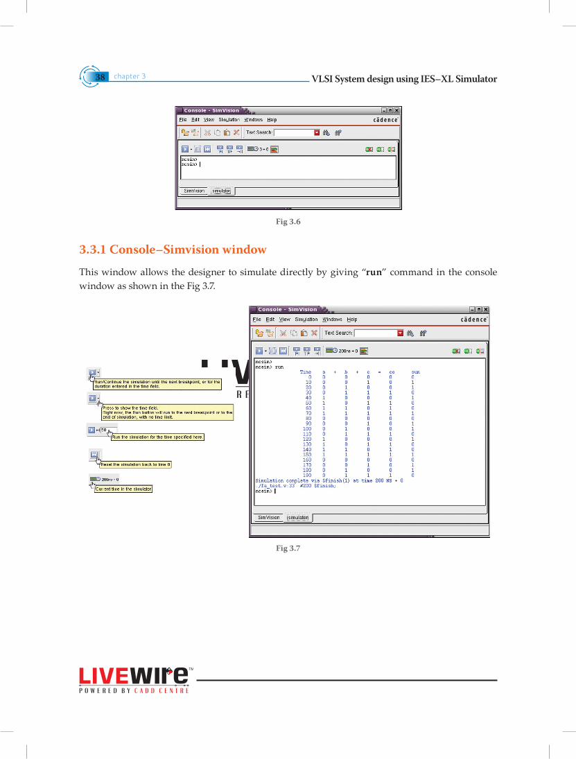
3.3.1 Console–Simvision window
This window allows the designer to simulate directly by giving “run” command in the console window as shown in the Fig 3.7.
Fig 3.7
VLSI System design using IES–XL Simulator chapter 3 39
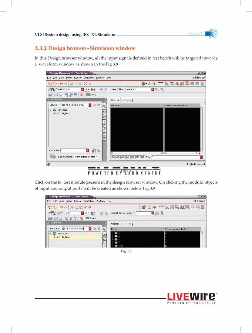
3.3.2 Design browser–Simvision window
In this Design browser window, all the input signals defined in test bench will be targeted towards a waveform window as shown in the Fig 3.8
Fig 3.8
Click on the fa_test module present in the design browser window. On clicking the module, objects of input and output ports will be created as shown below Fig 3.9,
Fig 3.9
VLSI System design using IES–XL Simulatorchapter 340
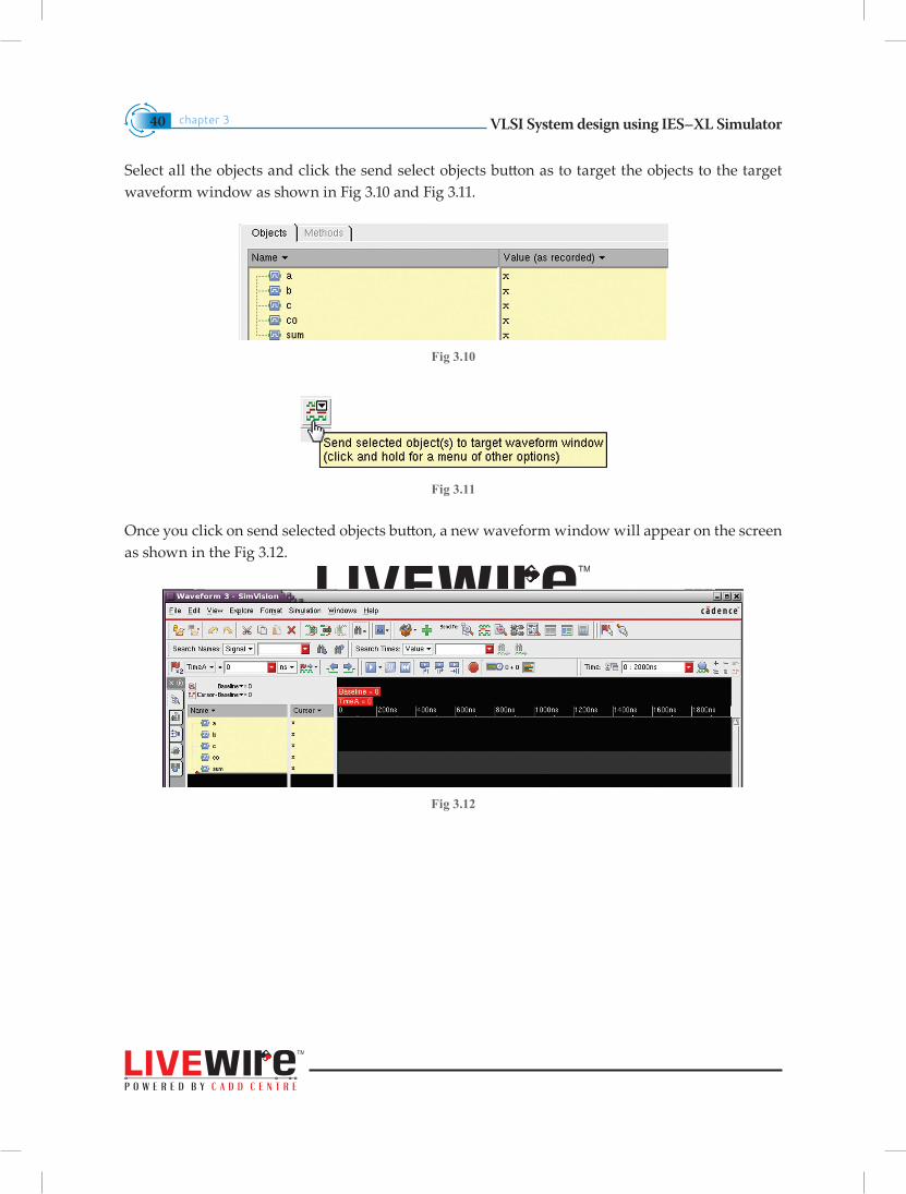
Select all the objects and click the send select objects button as to target the objects to the target waveform window as shown in Fig 3.10 and Fig 3.11.
Fig 3.10
Fig 3.11
Once you click on send selected objects button, a new waveform window will appear on the screen as shown in the Fig 3.12.
Fig 3.12
VLSI System design using IES–XL Simulator chapter 3 41
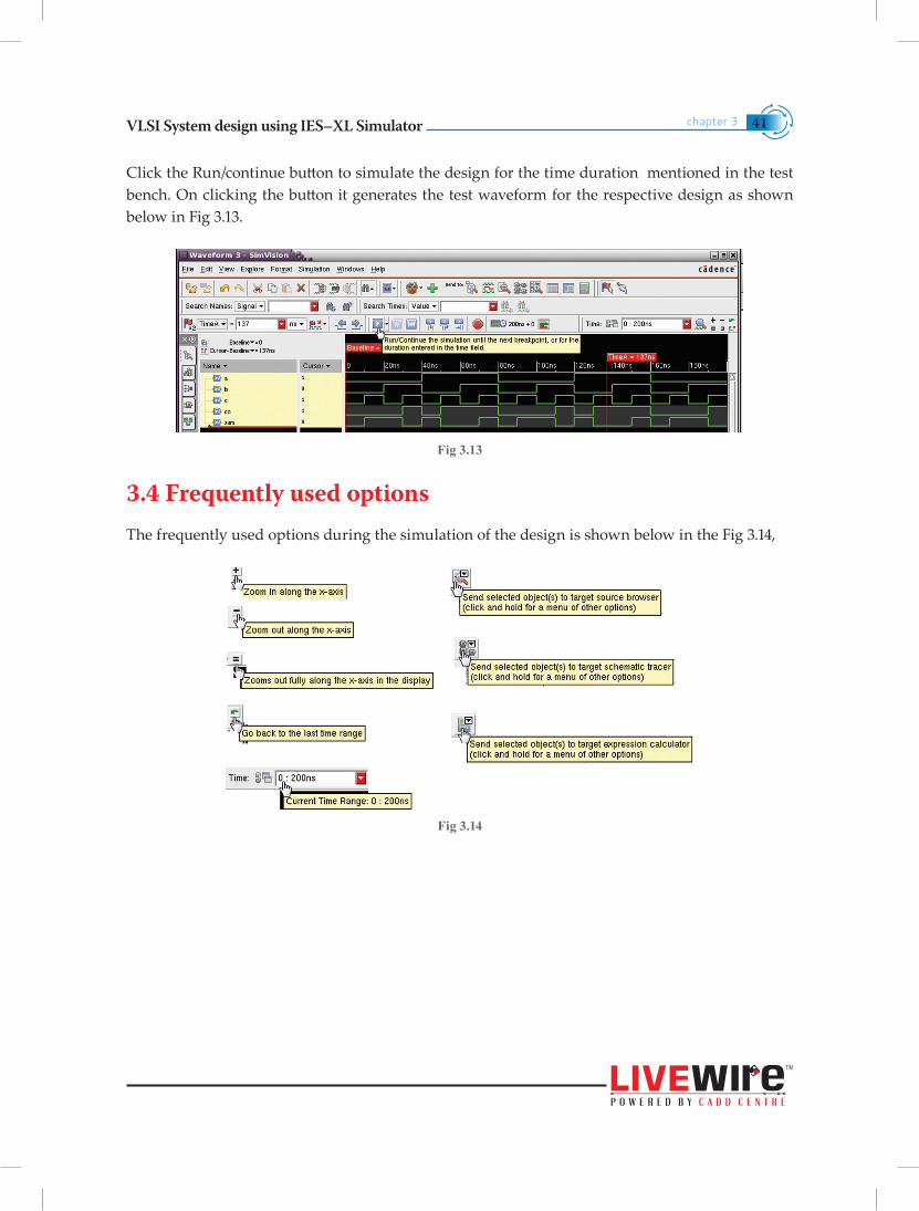
Click the Run/continue button to simulate the design for the time duration mentioned in the test bench. On clicking the button it generates the test waveform for the respective design as shown below in Fig 3.13.
Fig 3.13
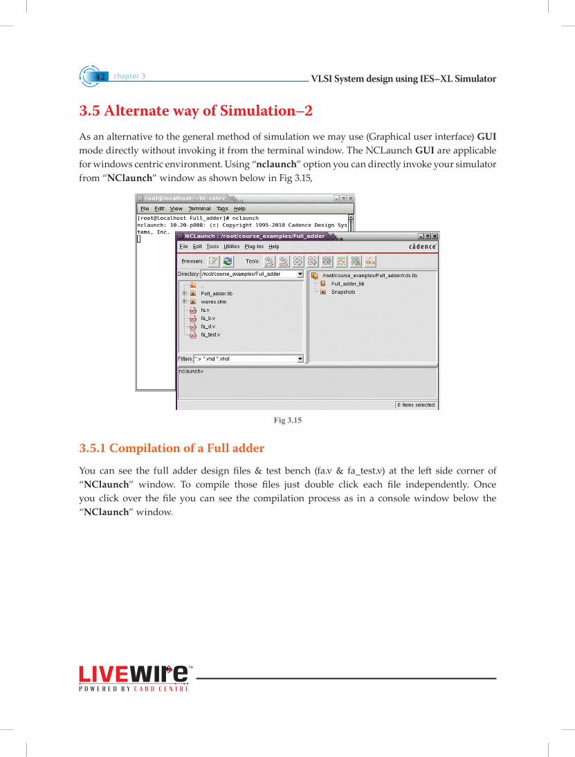
3.4 Frequently used optionsThe frequently used options during the simulation of the design is shown below in the Fig 3.14,
Fig 3.14
VLSI System design using IES–XL Simulatorchapter 342
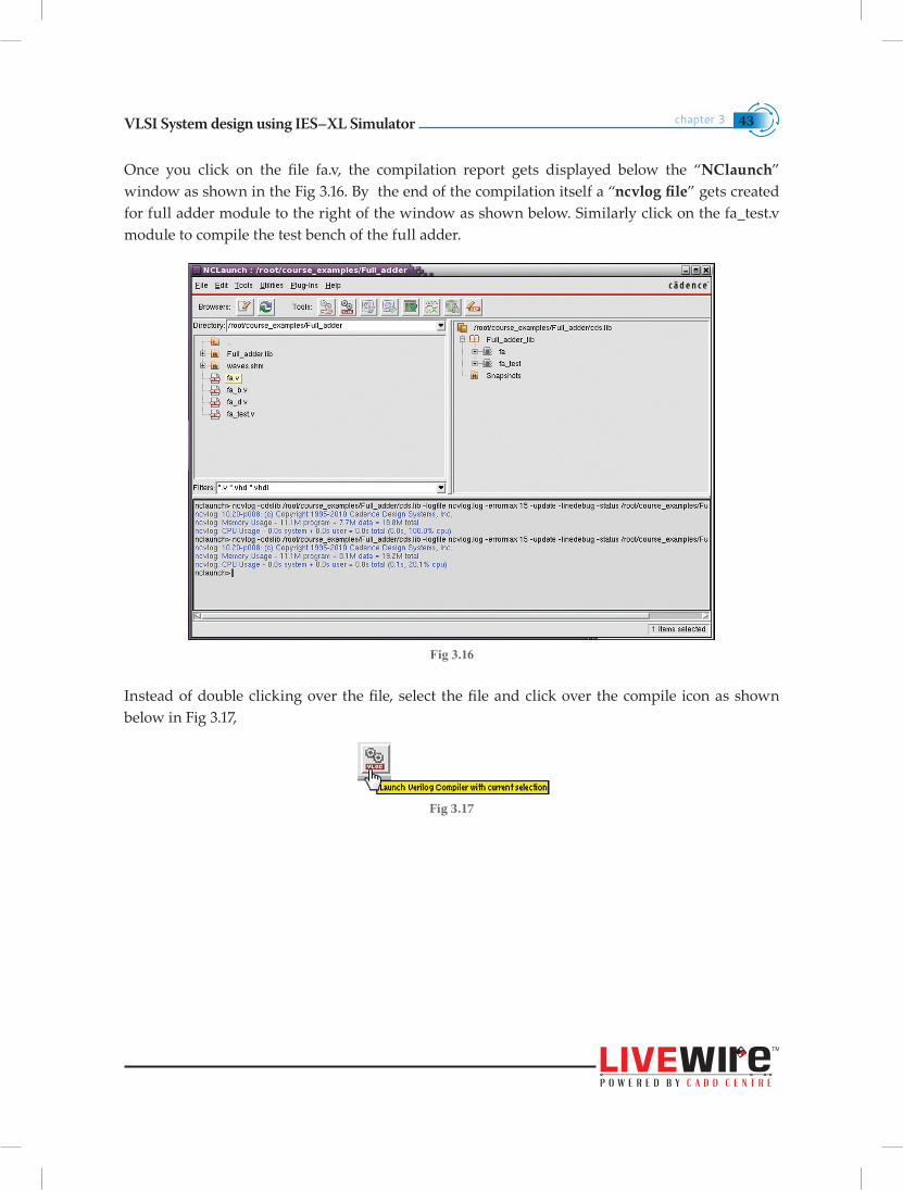
3.5 Alternate way of Simulation–2As an alternative to the general method of simulation we may use (Graphical user interface) GUI mode directly without invoking it from the terminal window. The NCLaunch GUI are applicable for windows centric environment. Using “nclaunch” option you can directly invoke your simulator from “NClaunch” window as shown below in Fig 3.15,
Fig 3.15
3.5.1 Compilation of a Full adder
You can see the full adder design files & test bench (fa.v & fa_test.v) at the left side corner of “NClaunch” window. To compile those files just double click each file independently. Once you click over the file you can see the compilation process as in a console window below the “NClaunch” window.
VLSI System design using IES–XL Simulator chapter 3 43
Once you click on the file fa.v, the compilation report gets displayed below the “NClaunch” window as shown in the Fig 3.16. By the end of the compilation itself a “ncvlog file” gets created for full adder module to the right of the window as shown below. Similarly click on the fa_test.v module to compile the test bench of the full adder.
Fig 3.16
Instead of double clicking over the file, select the file and click over the compile icon as shown below in Fig 3.17,
Fig 3.17
VLSI System design using IES–XL Simulatorchapter 344
3.5.2 Elaboration of Full adder
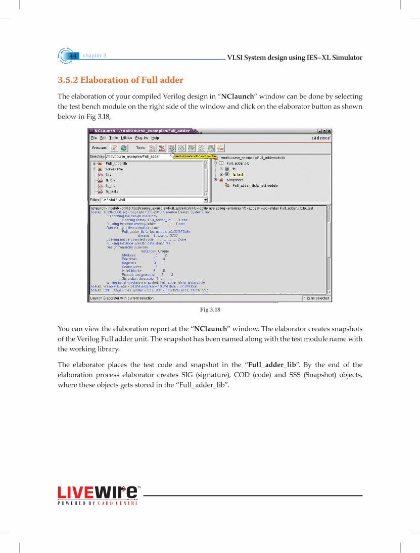
The elaboration of your compiled Verilog design in “NClaunch” window can be done by selecting the test bench module on the right side of the window and click on the elaborator button as shown below in Fig 3.18,
Fig 3.18
You can view the elaboration report at the “NClaunch” window. The elaborator creates snapshots of the Verilog Full adder unit. The snapshot has been named along with the test module name with the working library.
The elaborator places the test code and snapshot in the “Full_adder_lib”. By the end of the elaboration process elaborator creates SIG (signature), COD (code) and SSS (Snapshot) objects, where these objects gets stored in the “Full_adder_lib”.
VLSI System design using IES–XL Simulator chapter 3 45
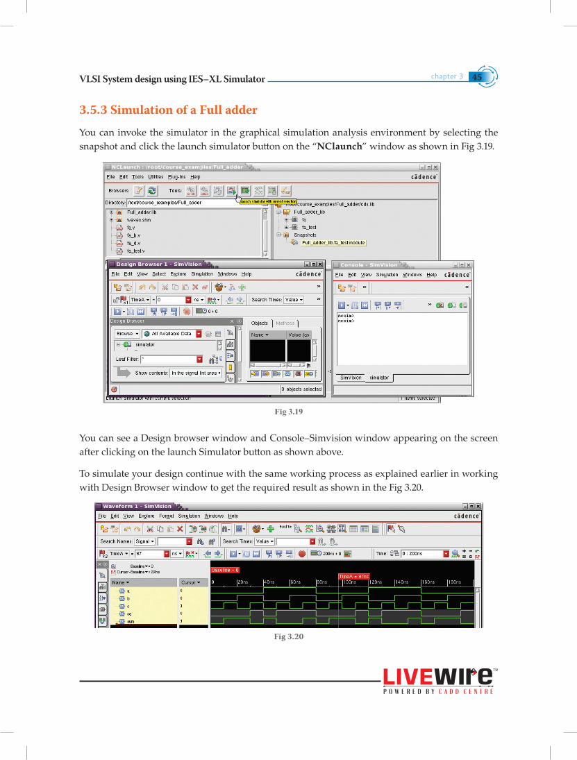
3.5.3 Simulation of a Full adder
You can invoke the simulator in the graphical simulation analysis environment by selecting the snapshot and click the launch simulator button on the “NClaunch” window as shown in Fig 3.19.
Fig 3.19
You can see a Design browser window and Console–Simvision window appearing on the screen after clicking on the launch Simulator button as shown above.
To simulate your design continue with the same working process as explained earlier in working with Design Browser window to get the required result as shown in the Fig 3.20.
Fig 3.20
VLSI System design using IES–XL Simulatorchapter 346
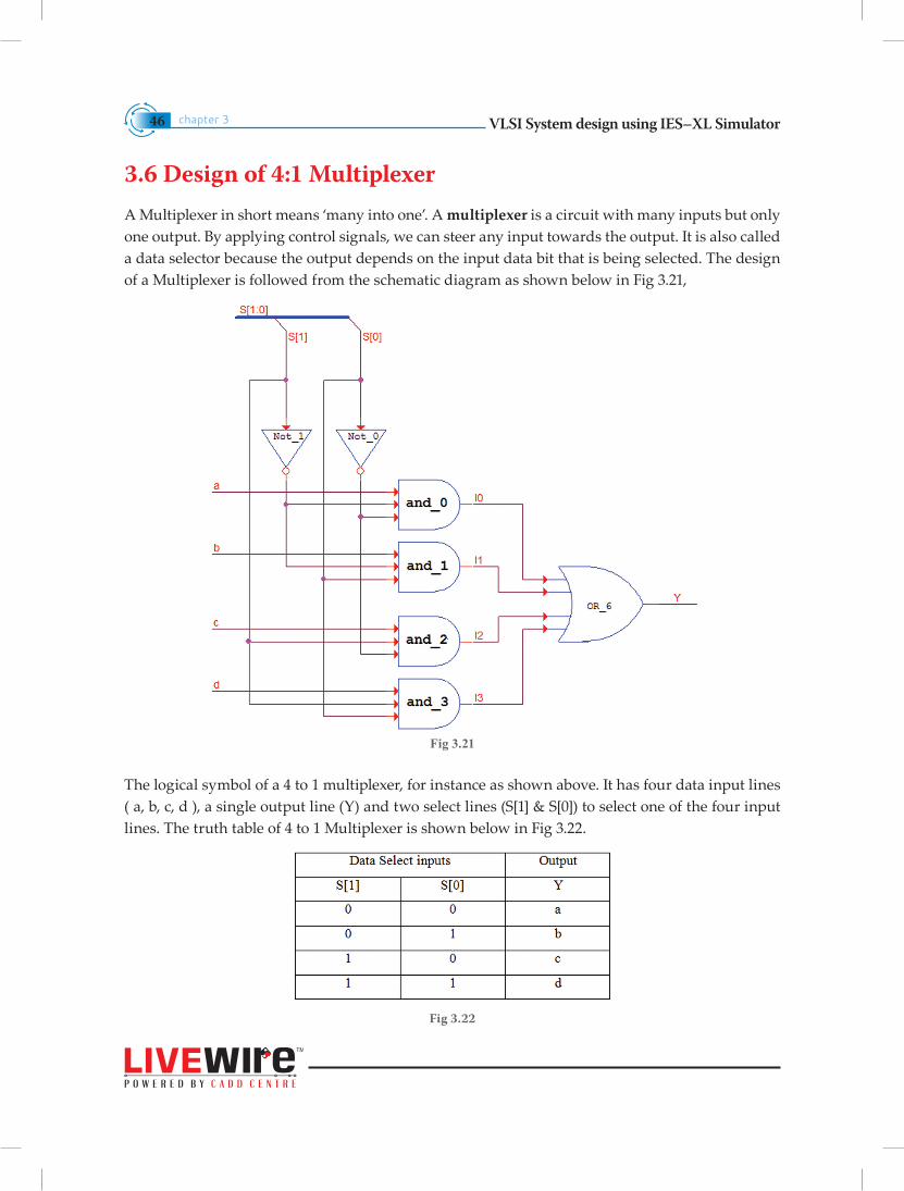
3.6 Design of 4:1 MultiplexerA Multiplexer in short means ‘many into one’. A multiplexer is a circuit with many inputs but only one output. By applying control signals, we can steer any input towards the output. It is also called a data selector because the output depends on the input data bit that is being selected. The design of a Multiplexer is followed from the schematic diagram as shown below in Fig 3.21,
Fig 3.21
The logical symbol of a 4 to 1 multiplexer, for instance as shown above. It has four data input lines ( a, b, c, d ), a single output line (Y) and two select lines (S[1] & S[0]) to select one of the four input lines. The truth table of 4 to 1 Multiplexer is shown below in Fig 3.22.
Fig 3.22
VLSI System design using IES–XL Simulator chapter 3 47
The output “Y = data input”, if and only based on the Selector line “S”
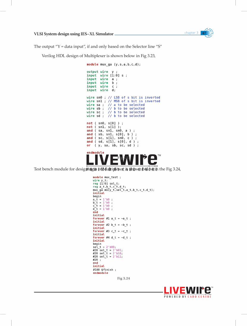
Verilog HDL design of Multiplexer is shown below in Fig 3.23,
Fig 3.23
Test bench module for designing a of Multiplexer is shown below in the Fig 3.24,
Fig 3.24
VLSI System design using IES–XL Simulatorchapter 348
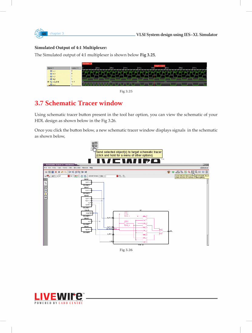
Simulated Output of 4:1 Multiplexer:The Simulated output of 4:1 multiplexer is shown below Fig 3.25,
Fig 3.25
3.7 Schematic Tracer windowUsing schematic tracer button present in the tool bar option, you can view the schematic of your HDL design as shown below in the Fig 3.26.
Once you click the button below, a new schematic tracer window displays signals in the schematic as shown below,
Fig 3.26
VLSI System design using IES–XL Simulator chapter 3 49
3.8 User Defined PrimitivesVerilog has built–in primitives like gates, transmission gates, and switches. This is a rather small number of primitives; if we need more complex primitives, then Verilog provides UDP, or simply User Defined Primitives, where it allows the user to define his own primitives. These UDP’s are self contained & are instantiated like gate level primitives. There are two types of UDP’s
• Combinational Logic UDP
• Sequential Logic UDP
We can include the timing information along with these UDP to model complete ASIC library models.
3.8.1 UDP Port Rules
• UDP’s can take only scalar input terminals (1 bit),
• Multiple input terminals are permitted in an UDP,
• They can have ONLY 1–bit scalar output,
• Output terminal must appear first in the terminal list,
• Multiple output terminals are disallowed,
• Inputs are declared with a keyword “input”, Outputs is declared with a keyword “output”
Note UDP’s do not support inout ports.
• In sequential UDP’s, the output is declared as reg,
• The state in a sequential UDP can be initialized with an initial statement. This statement is optional,
• State table defines the state of output under different input conditions. It can have entries, which contain values such as ‘0’, ‘1’ or ‘x’. Where ‘z’ values passed to the UDP are treated as ‘x’
• UDP’s are defined at the same level as that of modules. UDP’s cannot be defined within modules, they can only be instantiated just like gate primitives.
VLSI System design using IES–XL Simulatorchapter 350
3.8.2 UDP format
As UDPs cannot be defined within the modules, they can only be instantiated within them. The design block of a UDP is shown in the Fig 3.27
• A UDP definition starts with the keyword primitive,
• The primitive name, output terminal and input terminals are specified,
• Terminals are declared as output or input in the terminal declaration section,
• For sequential UDP’s there is an optional initial statement that initializes the output terminal of UDP,
• UDP state table is the most important part of the UDP. Keywords used are table and end table
Fig 3.27
Primitive definition is completed with the keyword “endprimitve”.
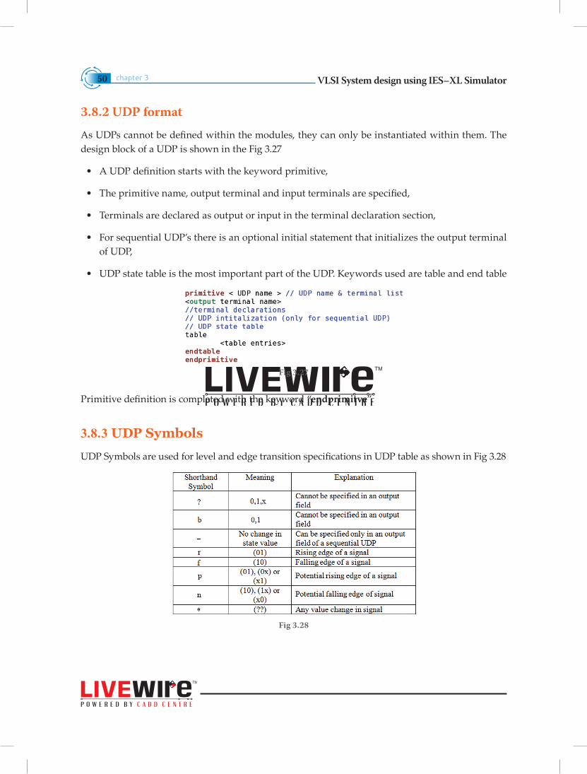
3.8.3 UDP Symbols
UDP Symbols are used for level and edge transition specifications in UDP table as shown in Fig 3.28
Fig 3.28
VLSI System design using IES–XL Simulator chapter 3 51
3.8.4 USER DEFINED PRIMITIVES Examples
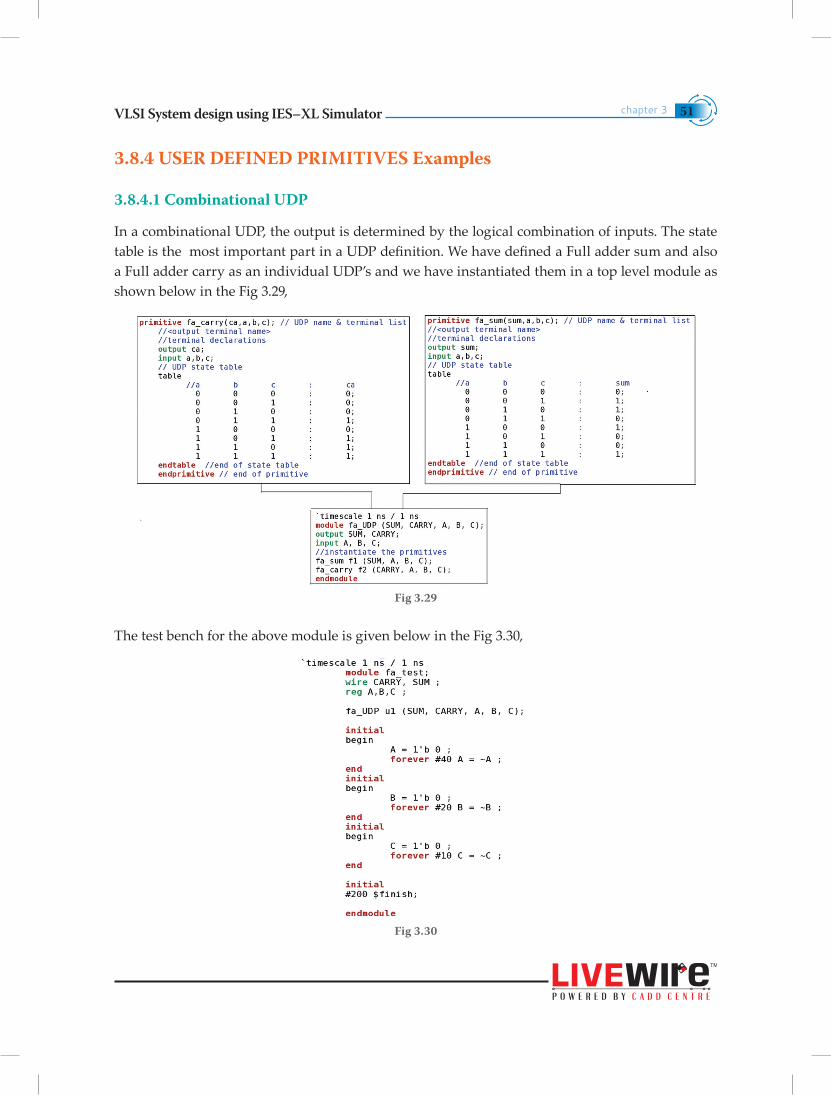
3.8.4.1 Combinational UDP
In a combinational UDP, the output is determined by the logical combination of inputs. The state table is the most important part in a UDP definition. We have defined a Full adder sum and also a Full adder carry as an individual UDP’s and we have instantiated them in a top level module as shown below in the Fig 3.29,
Fig 3.29
The test bench for the above module is given below in the Fig 3.30,
Fig 3.30
VLSI System design using IES–XL Simulatorchapter 352
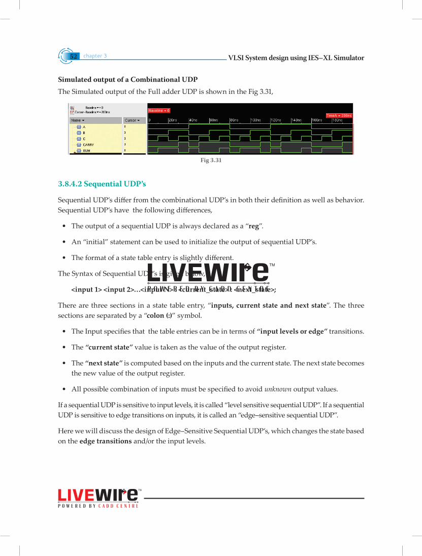
Simulated output of a Combinational UDPThe Simulated output of the Full adder UDP is shown in the Fig 3.31,
Fig 3.31
3.8.4.2 Sequential UDP’s
Sequential UDP’s differ from the combinational UDP’s in both their definition as well as behavior. Sequential UDP’s have the following differences,
• The output of a sequential UDP is always declared as a “reg”.
• An “initial” statement can be used to initialize the output of sequential UDP’s.
• The format of a state table entry is slightly different.
The Syntax of Sequential UDP’s is given below,
<input 1> <input 2>…<input N> : <current_state> : <next_state>;
There are three sections in a state table entry, “inputs, current state and next state”. The three sections are separated by a “colon (:)” symbol.
• The Input specifies that the table entries can be in terms of “input levels or edge” transitions.
• The “current state” value is taken as the value of the output register.
• The “next state” is computed based on the inputs and the current state. The next state becomes the new value of the output register.
• All possible combination of inputs must be specified to avoid unknown output values.
If a sequential UDP is sensitive to input levels, it is called “level sensitive sequential UDP”. If a sequential UDP is sensitive to edge transitions on inputs, it is called an “edge–sensitive sequential UDP”.
Here we will discuss the design of Edge–Sensitive Sequential UDP’s, which changes the state based on the edge transitions and/or the input levels.
VLSI System design using IES–XL Simulator chapter 3 53
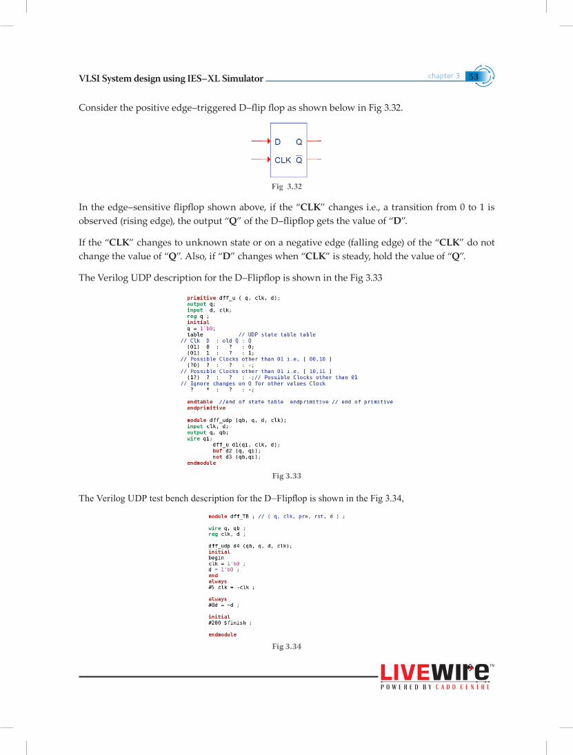
Consider the positive edge–triggered D–flip flop as shown below in Fig 3.32.
Fig 3.32
In the edge–sensitive flipflop shown above, if the “CLK” changes i.e., a transition from 0 to 1 is observed (rising edge), the output “Q” of the D–flipflop gets the value of “D”.
If the “CLK” changes to unknown state or on a negative edge (falling edge) of the “CLK” do not change the value of “Q”. Also, if “D” changes when “CLK” is steady, hold the value of “Q”.
The Verilog UDP description for the D–Flipflop is shown in the Fig 3.33
Fig 3.33
The Verilog UDP test bench description for the D–Flipflop is shown in the Fig 3.34,
Fig 3.34
VLSI System design using IES–XL Simulatorchapter 354
1. What do you mean by elaboration and simulation?
2. What do you understand by Console simvision window?
3. What do you understand by Design browser window?
4. What do you mean by UDP?
5. Define combinational UDP?
6. Define Sequential UDP?
7. Define the rules and regulations of defining an UDP?
This chapter helps
• Describe the features of elaboration and simulation of the design,
• Understand How to invoke the elaboration and simulation process,
• Learn the Alternate way of simulating a digital design using the tool,
• Understand UDP definition rules and parts of UDP definition,
• Define sequential and combinational UDP’s and Identify UDP shorthand symbols for more conciseness and guidelines for the UDP design.
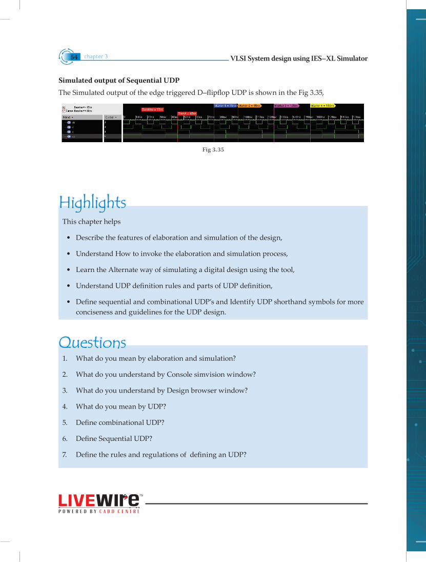
Simulated output of Sequential UDPThe Simulated output of the edge triggered D–flipflop UDP is shown in the Fig 3.35,
Fig 3.35
Highlights
Questions

DATAFLOW MODELING 4

DATAFLOW MODELING
INTRODUCTION
This chapter deals with a higher level of abstraction than that
in the gate level modeling. Dataflow modeling consists of
continuous assignments that replaces the primitive gates with
expressions. Operations, operands etc., which form the basis
of dataflow modeling are discussed on their various types,
along with the procedure to work on them. Further design
methodology for a multiplexer is also given in this chapter.
VLSI System design using IES–XL Simulatorchapter 458
4.1 Introduction to Dataflow ModelingThe designers can design more effectively if they concentrate on implementing functions at a level of abstraction higher than the gate level. This approach allows the designer to concentrate on optimizing the circuit in terms of data flow.
Rapid increase in the chips density has resulted, data flow modeling in gaining great importance. The designer concentrates in optimizing the circuit in terms of data flow. Dataflow modeling has become a popular design approach as logic synthesis tools have become sophisticated
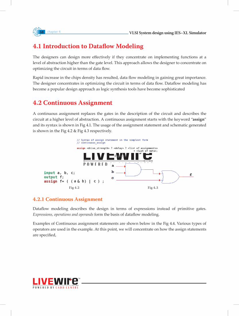
4.2 Continuous AssignmentA continuous assignment replaces the gates in the description of the circuit and describes the circuit at a higher level of abstraction. A continuous assignment starts with the keyword “assign” and its syntax is shown in Fig 4.1. The usage of the assignment statement and schematic generated is shown in the Fig 4.2 & Fig 4.3 respectively.
Fig 4.1
Fig 4.2 Fig 4.3
4.2.1 Continuous Assignment
Dataflow modeling describes the design in terms of expressions instead of primitive gates. Expressions, operations and operands form the basis of dataflow modeling.
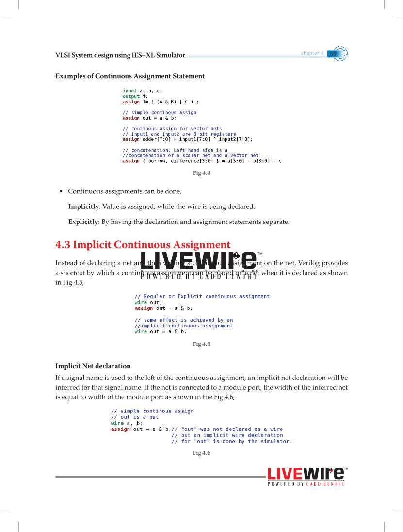
Examples of Continuous assignment statements are shown below in the Fig 4.4. Various types of operators are used in the example. At this point, we will concentrate on how the assign statements are specified,
VLSI System design using IES–XL Simulator chapter 4 59
Examples of Continuous Assignment Statement
Fig 4.4
• Continuous assignments can be done,
Implicitly: Value is assigned, while the wire is being declared.
Explicitly: By having the declaration and assignment statements separate.
4.3 Implicit Continuous AssignmentInstead of declaring a net and then writing a continuous assignment on the net, Verilog provides a shortcut by which a continuous assignment can be placed on a net when it is declared as shown in Fig 4.5,
Fig 4.5
Implicit Net declarationIf a signal name is used to the left of the continuous assignment, an implicit net declaration will be inferred for that signal name. If the net is connected to a module port, the width of the inferred net is equal to width of the module port as shown in the Fig 4.6,
Fig 4.6
VLSI System design using IES–XL Simulatorchapter 460
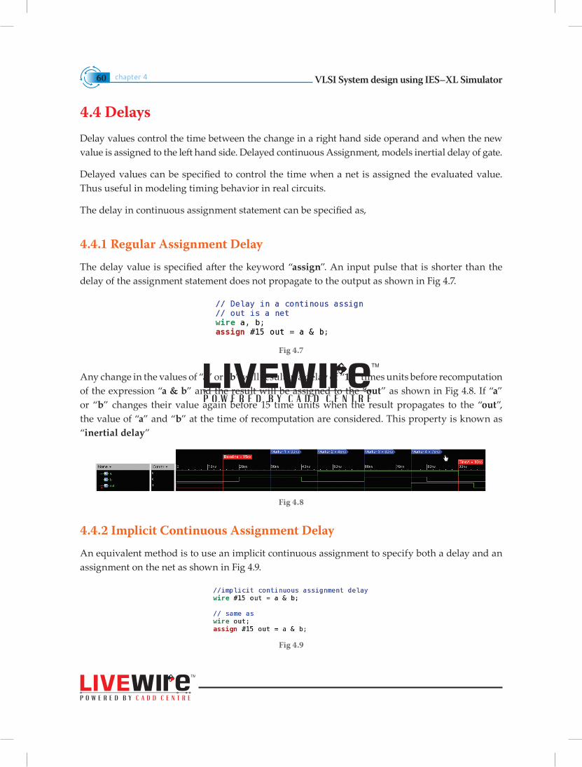
4.4 DelaysDelay values control the time between the change in a right hand side operand and when the new value is assigned to the left hand side. Delayed continuous Assignment, models inertial delay of gate.
Delayed values can be specified to control the time when a net is assigned the evaluated value. Thus useful in modeling timing behavior in real circuits.
The delay in continuous assignment statement can be specified as,
4.4.1 Regular Assignment Delay
The delay value is specified after the keyword “assign”. An input pulse that is shorter than the delay of the assignment statement does not propagate to the output as shown in Fig 4.7.
Fig 4.7
Any change in the values of “a” or “b” will result in a delay of “15” times units before recomputation of the expression “a & b” and the result will be assigned to the “out” as shown in Fig 4.8. If “a” or “b” changes their value again before 15 time units when the result propagates to the “out”, the value of “a” and “b” at the time of recomputation are considered. This property is known as “inertial delay”
Fig 4.8
4.4.2 Implicit Continuous Assignment Delay
An equivalent method is to use an implicit continuous assignment to specify both a delay and an assignment on the net as shown in Fig 4.9.
Fig 4.9
VLSI System design using IES–XL Simulator chapter 4 61
The declaration above has the same effect as defining a “wire out” and declaring a continuous assignment on “out”.
4.4.3 Net Declaration Delay
A delay can be specified on a net when it is declared without putting a continuous assignment on the net too. If a delay is specified on a net out, then any value change applied to the net out is delayed accordingly as shown in Fig 4.10,
Fig 4.10
4.5 Operators and OperandsDataflow modeling describes the design in terms of expressions instead of primitive gates. Expressions, operators and operands from the basis of dataflow modeling.
4.5.1 Arithmetic Operators
There are two types of arithmetic operators, binary and unary.
• Binary Operators: +,–, *, /, % (the modulus operator),
• Unary: +,–(This is used to specify the sign),
• Integer division truncates any fractional part,
• The result of a modulus operation takes the sign of the first operand,
• If any operand bit value is the unknown value “x”, then the entire result value is also “x”,
• Register data types are used as unsigned values (Negative numbers are stored in two’s complement form).
VLSI System design using IES–XL Simulatorchapter 462
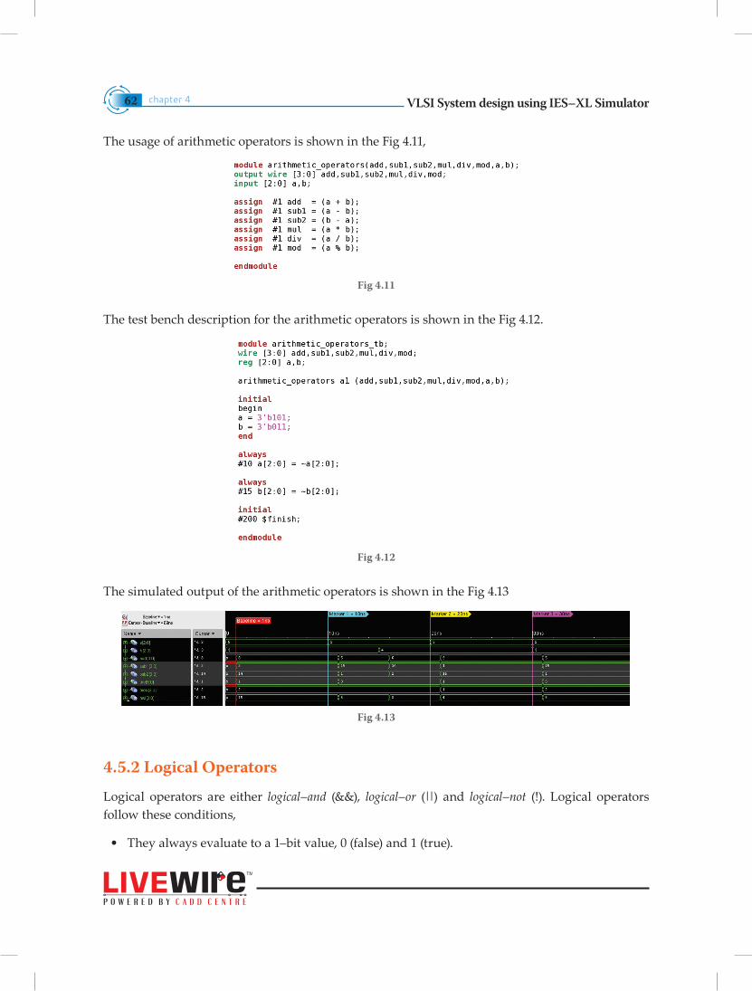
The usage of arithmetic operators is shown in the Fig 4.11,
Fig 4.11
The test bench description for the arithmetic operators is shown in the Fig 4.12.
Fig 4.12
The simulated output of the arithmetic operators is shown in the Fig 4.13
Fig 4.13
4.5.2 Logical Operators
Logical operators are either logical–and (&&), logical–or (||) and logical–not (!). Logical operators follow these conditions,
• They always evaluate to a 1–bit value, 0 (false) and 1 (true).
VLSI System design using IES–XL Simulator chapter 4 63
• If an operand is not equal to zero, it is equivalent to a logical “1” (true condition), if it is equal to zero, it is equivalent to a logical “0” (false condition). If any operand bit is “x or z”, it is equivalent to “x” and it is normally treated by simulator as a false condition.
• Expressions connected by “&&” and “||” are evaluated from left to right
• Evaluation stops as soon as the result is known
• The result is a scalar value:
x “0” if the relation is false
x “1” if the relation is true & “x” if any of the operands has “x” (unknown) bits
The usage of logical operators is shown in the Fig 4.14,
Fig 4.14
The test bench description for the logical operators is shown in the Fig 4.15
Fig 4.15
VLSI System design using IES–XL Simulatorchapter 464
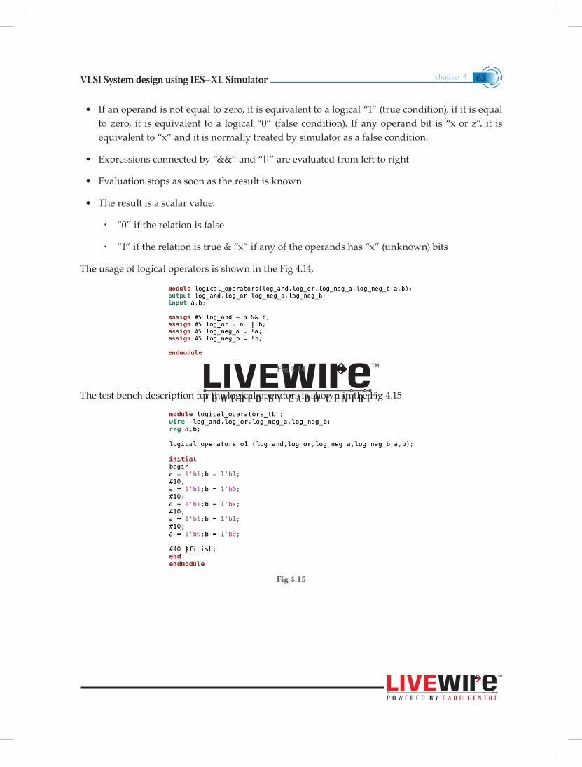
The simulated output of the logical operators is shown in the Fig 4.16.
Fig 4.16
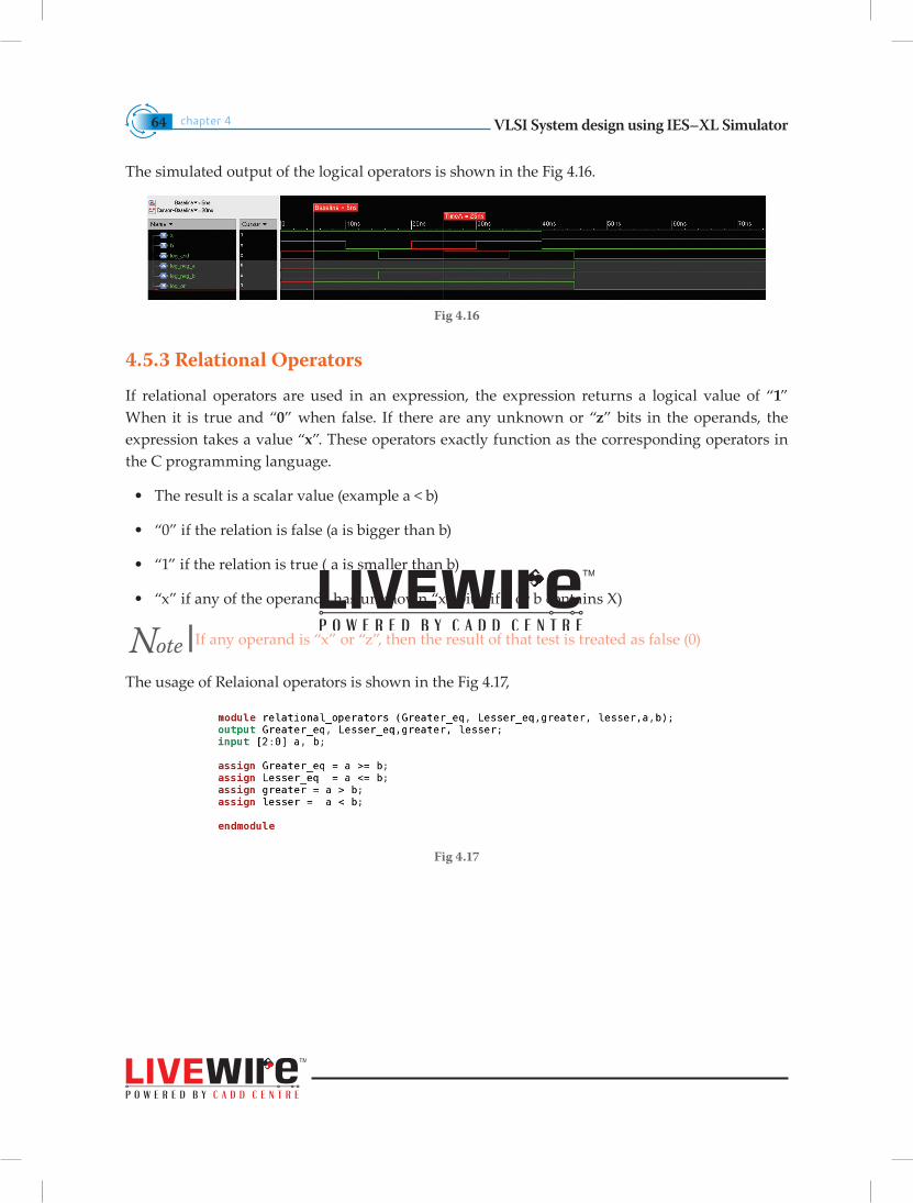
4.5.3 Relational Operators
If relational operators are used in an expression, the expression returns a logical value of “1” When it is true and “0” when false. If there are any unknown or “z” bits in the operands, the expression takes a value “x”. These operators exactly function as the corresponding operators in the C programming language.
• The result is a scalar value (example a < b)
• “0” if the relation is false (a is bigger than b)
• “1” if the relation is true ( a is smaller than b)
• “x” if any of the operands has unknown “x” bits (if a or b contains X)
Note If any operand is “x” or “z”, then the result of that test is treated as false (0)
The usage of Relaional operators is shown in the Fig 4.17,
Fig 4.17
VLSI System design using IES–XL Simulator chapter 4 65
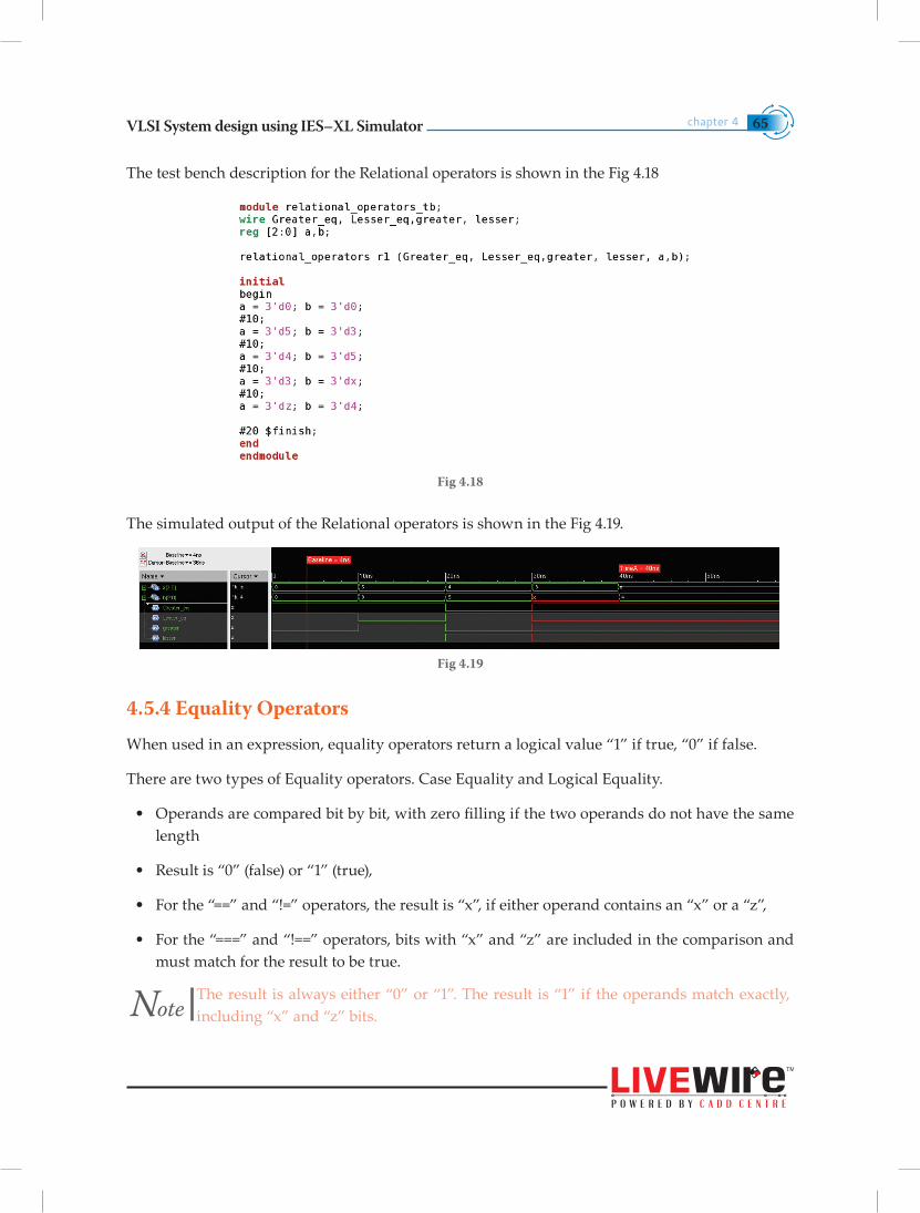
The test bench description for the Relational operators is shown in the Fig 4.18
Fig 4.18
The simulated output of the Relational operators is shown in the Fig 4.19.
Fig 4.19
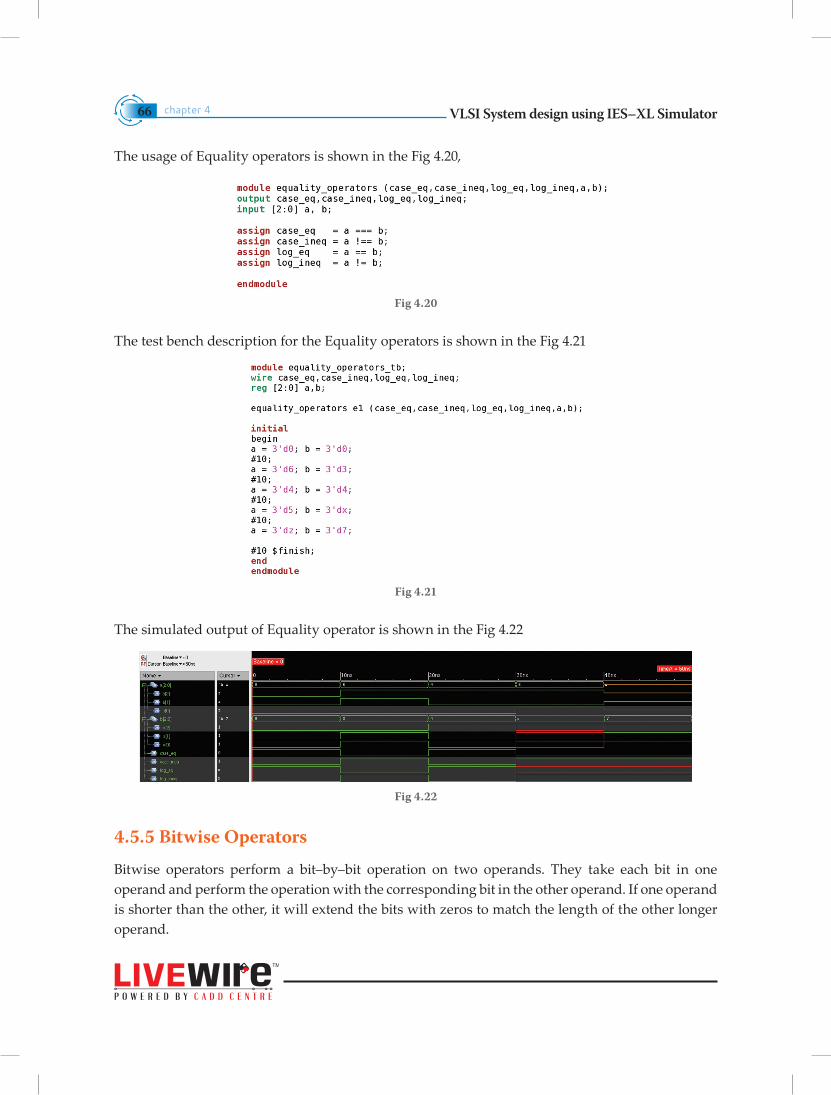
4.5.4 Equality Operators
When used in an expression, equality operators return a logical value “1” if true, “0” if false.
There are two types of Equality operators. Case Equality and Logical Equality.
• Operands are compared bit by bit, with zero filling if the two operands do not have the same length
• Result is “0” (false) or “1” (true),
• For the “==” and “!=” operators, the result is “x”, if either operand contains an “x” or a “z”,
• For the “===” and “!==” operators, bits with “x” and “z” are included in the comparison and must match for the result to be true.
NoteThe result is always either “0” or “1”. The result is “1” if the operands match exactly, including “x” and “z” bits.
VLSI System design using IES–XL Simulatorchapter 466
The usage of Equality operators is shown in the Fig 4.20,
Fig 4.20
The test bench description for the Equality operators is shown in the Fig 4.21
Fig 4.21
The simulated output of Equality operator is shown in the Fig 4.22
Fig 4.22
4.5.5 Bitwise Operators
Bitwise operators perform a bit–by–bit operation on two operands. They take each bit in one operand and perform the operation with the corresponding bit in the other operand. If one operand is shorter than the other, it will extend the bits with zeros to match the length of the other longer operand.
VLSI System design using IES–XL Simulator chapter 4 67
• Computations include unknown bits, in the following manner :
x ~x = x
x 0 & x = 0
x 1 & x = x & x = x
x 1|x = 1
x 0|x = x|x = x
x 0^x = 1̂ x = x^x = x
x 0^~x = 1̂ ~x = x^~x = x
Logical Operators Bitwise OperatorsIt yield a logical value of 0,1,X It yield only a bit value
It does not provide its operation bit by bit. It provides bit by bit operation.
The usage of Bitwise operators is shown in the Fig 4.23,
Fig 4.23
The test bench description for the Bitwise operators is shown in the Fig 4.24
Fig 4.24
VLSI System design using IES–XL Simulatorchapter 468
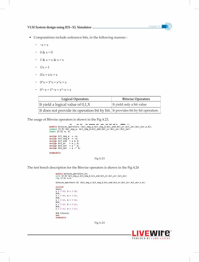
The simulated output of the Bitwise operators is shown in the Fig 4.25.
Fig 4.25
4.5.6 Reduction Operators
Reduction operators take only one operand at a time. They perform a bitwise operation on a single vector operand and yield a 1–bit result. Reduction unary NAND and NOR operators operate as AND and OR respectively, but only with their outputs negated.
The usage of Reduction operators is shown in the Fig 4.26,
Fig 4.26
The test bench description for the Reduction operators is shown in the Fig 4.27
Fig 4.27
VLSI System design using IES–XL Simulator chapter 4 69
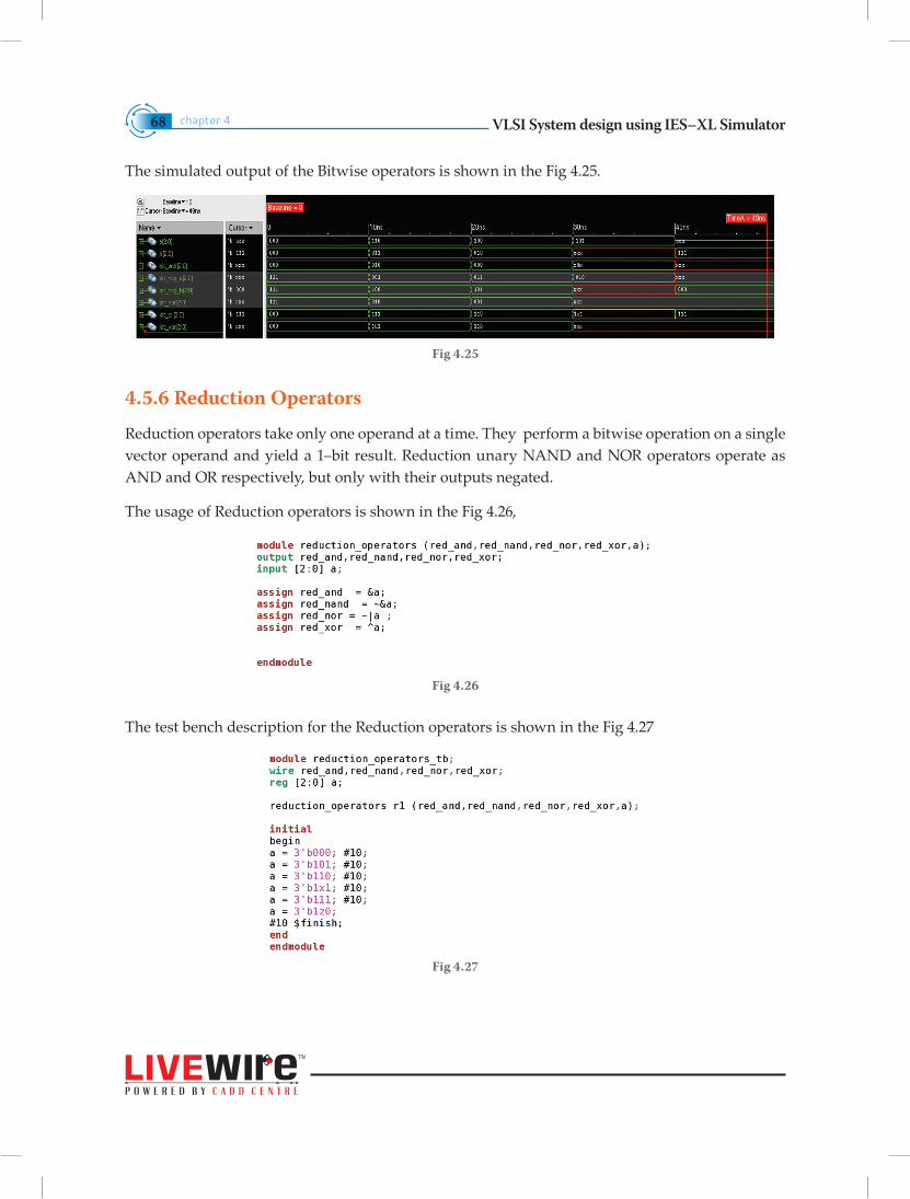
The simulated output of the Reduction operators is shown in the Fig 4.28.
Fig 4.28
4.5.7 Shift Operators
Regular shift operators shift a vector operand to the right or the left by a specified number of bits. The operands are the vectors and the number of bits to shift. When the bits are shifted, the vacant bit positions are filled with zeros. Shift operations do not wrap around. The usage of Shift operators is shown in the Fig 4.29,
Fig 4.29
The test bench description for the Shift operators is shown in the Fig 4.30,
Fig 4.30
VLSI System design using IES–XL Simulatorchapter 470
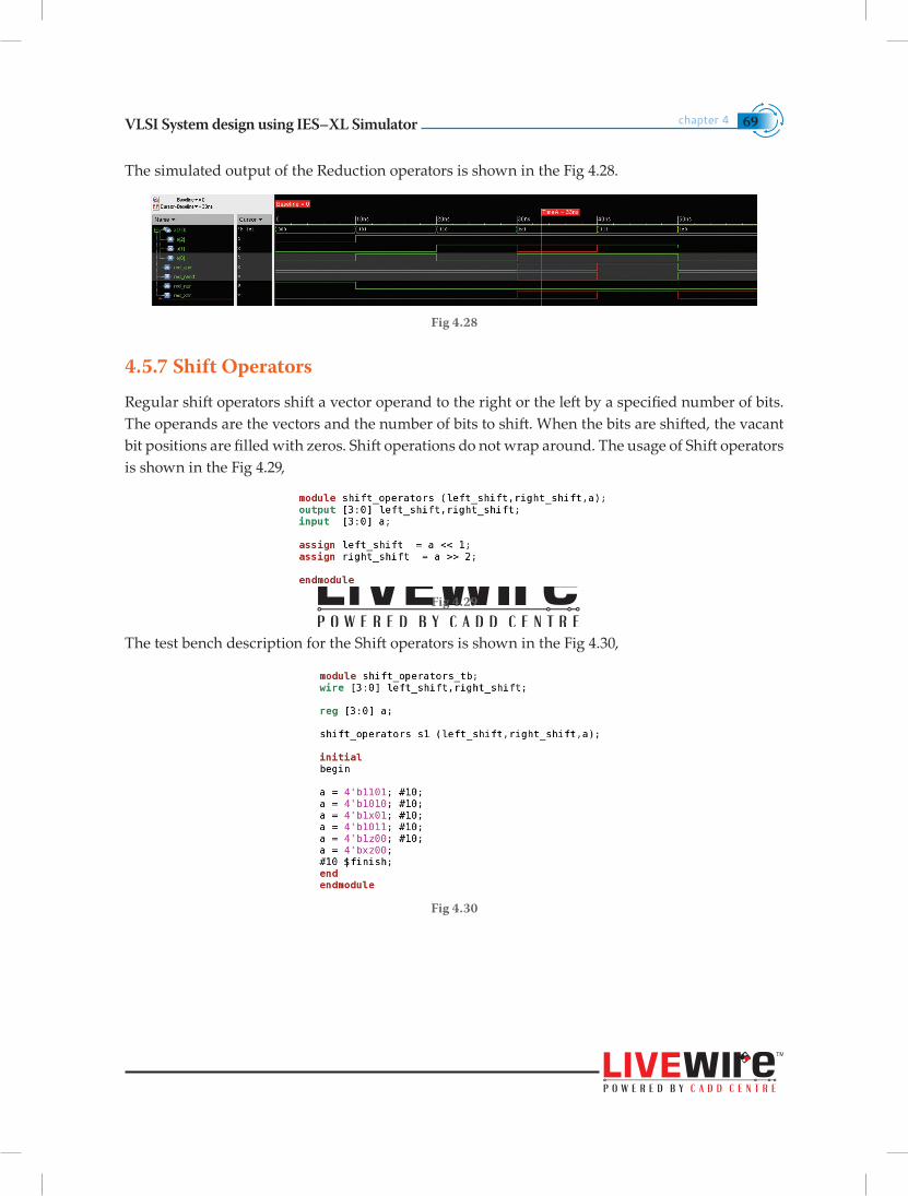
The simulated output of the Shift operators is shown in the Fig 4.31,
Fig 4.31
4.5.8 Concatenation Operators
This operator provides a mechanism to append multiple operands. The operands must be sized. Unsized operands are not allowed because the size of each operand must be known for computing the size of the result. The usage of concatenation operators is shown in the Fig 4.32,
Fig 4.32
The test bench description for the Concatenation operators is shown in the Fig 4.33,
Fig 4.33
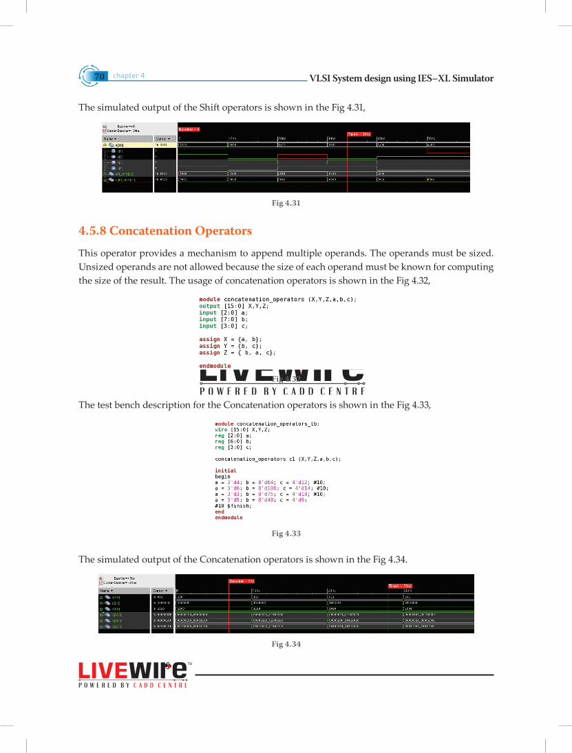
The simulated output of the Concatenation operators is shown in the Fig 4.34.
Fig 4.34
VLSI System design using IES–XL Simulator chapter 4 71
Concatenations are expressed as operands within braces, with commas separating the operands. Operands can be scalar nets or registers, vector nets or registers, bit–select, part select or sized constants.
4.5.9 Replication Operator
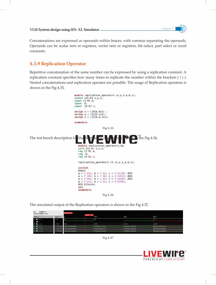
Repetitive concatenation of the same number can be expressed by using a replication constant. A replication constant specifies how many times to replicate the number within the brackets ( { } ). Nested concatenations and replication operator are possible. The usage of Replication operators is shown in the Fig 4.35,
Fig 4.35
The test bench description for the Replication operators is shown in the Fig 4.36,
Fig 4.36
The simulated output of the Replication operators is shown in the Fig 4.37,
Fig 4.37
VLSI System design using IES–XL Simulatorchapter 472
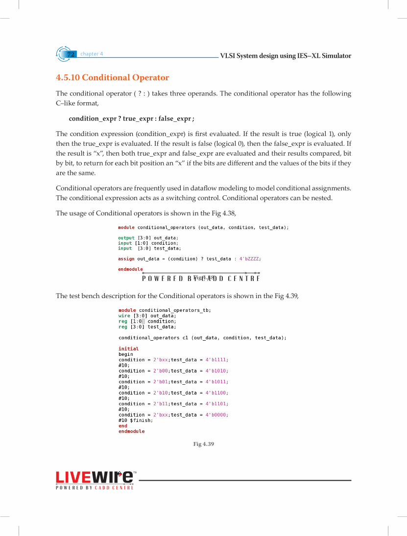
4.5.10 Conditional Operator
The conditional operator ( ? : ) takes three operands. The conditional operator has the following C–like format,
condition_expr ? true_expr : false_expr ;
The condition expression (condition_expr) is first evaluated. If the result is true (logical 1), only then the true_expr is evaluated. If the result is false (logical 0), then the false_expr is evaluated. If the result is “x”, then both true_expr and false_expr are evaluated and their results compared, bit by bit, to return for each bit position an “x” if the bits are different and the values of the bits if they are the same.
Conditional operators are frequently used in dataflow modeling to model conditional assignments. The conditional expression acts as a switching control. Conditional operators can be nested.
The usage of Conditional operators is shown in the Fig 4.38,
Fig 4.38
The test bench description for the Conditional operators is shown in the Fig 4.39,
Fig 4.39
VLSI System design using IES–XL Simulator chapter 4 73
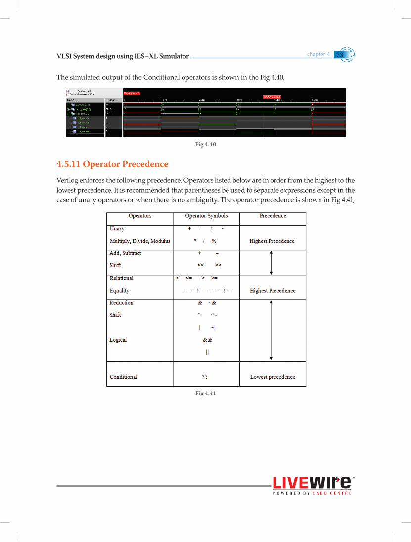
The simulated output of the Conditional operators is shown in the Fig 4.40,
Fig 4.40
4.5.11 Operator Precedence
Verilog enforces the following precedence. Operators listed below are in order from the highest to the lowest precedence. It is recommended that parentheses be used to separate expressions except in the case of unary operators or when there is no ambiguity. The operator precedence is shown in Fig 4.41,
Fig 4.41

VLSI System design using IES–XL Simulatorchapter 474
4.6 Designing an Octal–to–Binary EncoderAn octal to binary encoder accepts eight inputs and produces a three bit output code corresponding to the activated input. The truth table for the Octal to binary encoder is shown below in Fig 4.42,
Fig 4.42
The truth table shows that Bin [0] (LSB of Output code) must be 1 whenever the input,
Bin [0] = Oct[1] OR Oct[3] OR Oct[5] OR Oct[7],
Similarly,
Bin [1] = Oct[2] OR Oct[3] OR Oct[6] OR Oct[7],
Bin [2] = Oct[4] OR Oct[5] OR Oct[6] OR Oct[7].
The HDL design of the Octal to binary encoder is given below in Fig 4.43,
Fig 4.43
VLSI System design using IES–XL Simulator chapter 4 75
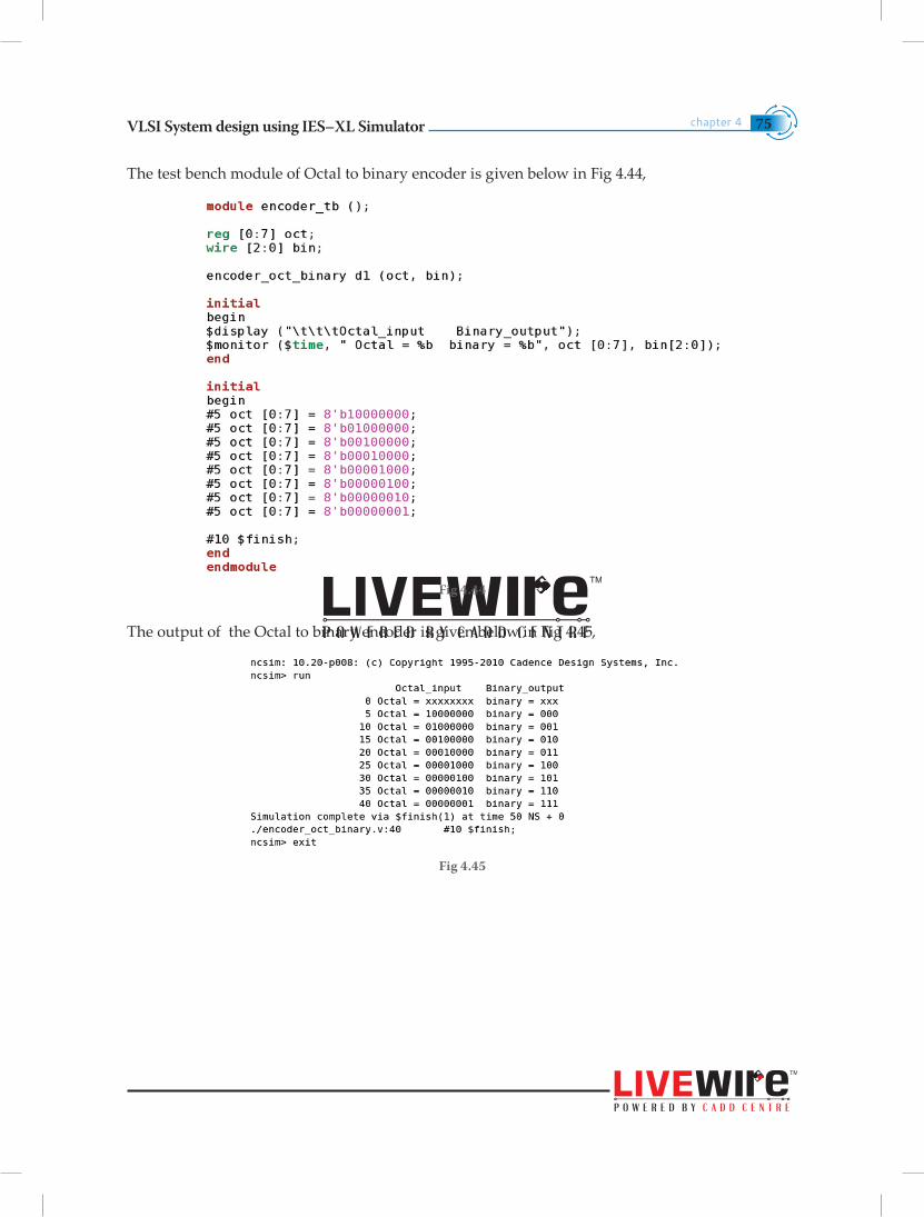
The test bench module of Octal to binary encoder is given below in Fig 4.44,
Fig 4.44
The output of the Octal to binary encoder is given below in Fig 4.45,
Fig 4.45
VLSI System design using IES–XL Simulatorchapter 476
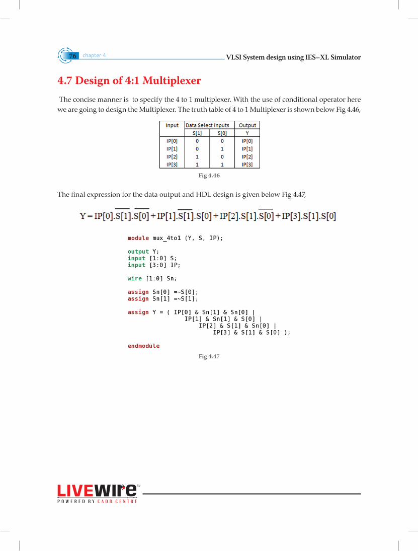
4.7 Design of 4:1 Multiplexer The concise manner is to specify the 4 to 1 multiplexer. With the use of conditional operator here we are going to design the Multiplexer. The truth table of 4 to 1 Multiplexer is shown below Fig 4.46,
Fig 4.46
The final expression for the data output and HDL design is given below Fig 4.47,
Fig 4.47
VLSI System design using IES–XL Simulator chapter 4 77
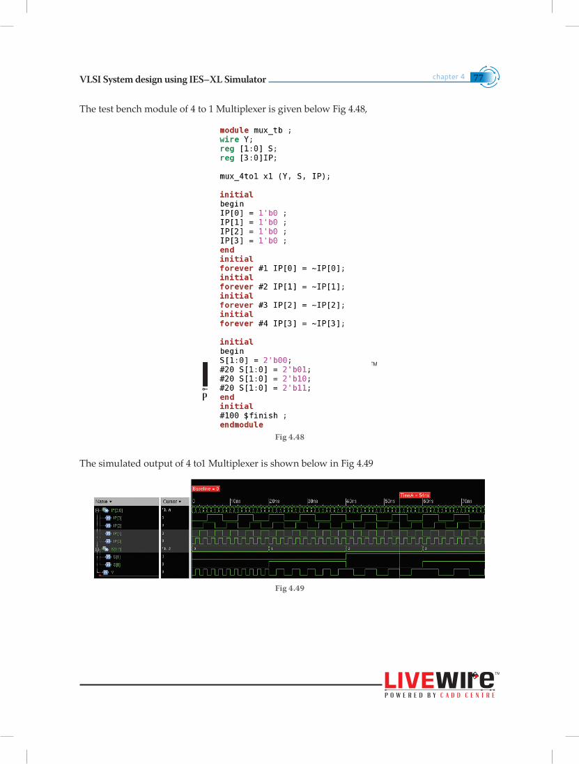
The test bench module of 4 to 1 Multiplexer is given below Fig 4.48,
Fig 4.48
The simulated output of 4 to1 Multiplexer is shown below in Fig 4.49
Fig 4.49
VLSI System design using IES–XL Simulatorchapter 478
1. What is the usage of Continuous Assignment statement in Data flow modeling?
2. What is the difference between the continuous & implicit continuous assignment statements?
3. Define implicit continuous Assignment Delay.
4. Define Expressions, Operators and Operands.
5. Differentiate the Logical Operators and Bitwise Operators.
6. Describe the functionality of Concatenation and Conditional Operator?
7. What do you mean by operators of Highest precedence and Lowest precedence?
The user learns
• Describing the usage of continuous assignment statement
• How to explain the usage of implicit assignment delay and net declaration delay for continuous assignment statements.
• How to explain the usage of assigning delays to operand
• How to define the expressions making use of the operators and operands.
• How to use dataflow constructs to model practical digital circuits
Highlights
Questions

BEHAVIORAL MODELING 5

BEHAVIORAL MODELING
INTRODUCTION
A higher level of abstraction is observed in the behavioral
modeling, in comparison to other two previously described
abstraction levels. The two predominant structural procedure
statements in Verilog, for behavioral modeling are explained.
Also the other procedural assignments, blocking and non–
blocking statements, timing controls, conditional statements,
loop statements and other attributes of behavioral modeling
in verilog such as sequential and parallel blocks, tasks and
functions are also detailed.
VLSI System design using IES–XL Simulatorchapter 582
5.1 Introduction to Behavioral ModelingThe architectural evaluation takes place at an algorithmic level while opting for behavioral modeling, where the designers do not necessarily think in terms of logic gates or data flow but in terms of the algorithm they wish to implement in the hardware itself.
Behavioral modeling describes the functionality in an algorithmic manner. After the architecture and algorithm are finalized, designers focus in building the digital circuit to implement the algorithm. The HDL Code is independent of vendor technology.
Design at this level resembles C programming more than it would resemble a digital circuit. Verilog is rich in behavioral constructs that provide the designer with great amount of flexibility.
5.2 Structured ProceduresThere are two structured procedural statements in Verilog
• Initial – This block execute only once at time zero (start execution at time zero).
• Always – This block executes over and over again; in other words, as the name suggests, it executes always.
Verilog is a concurrent programming language unlike the C programming language which is sequential in nature. The above mentioned two statements are basic statements in behavioral modeling. Each “always” and “initial” statements represents a separate activity flow in Verilog.
5.2.1 Initial Statement
If there are multiple “initial” blocks, each block starts to execute concurrently at time “0”. Multiple behavioral statements must be grouped, typically using the keyword “begin” and “end”. It is activated at the beginning of the simulation.
VLSI System design using IES–XL Simulator chapter 5 83
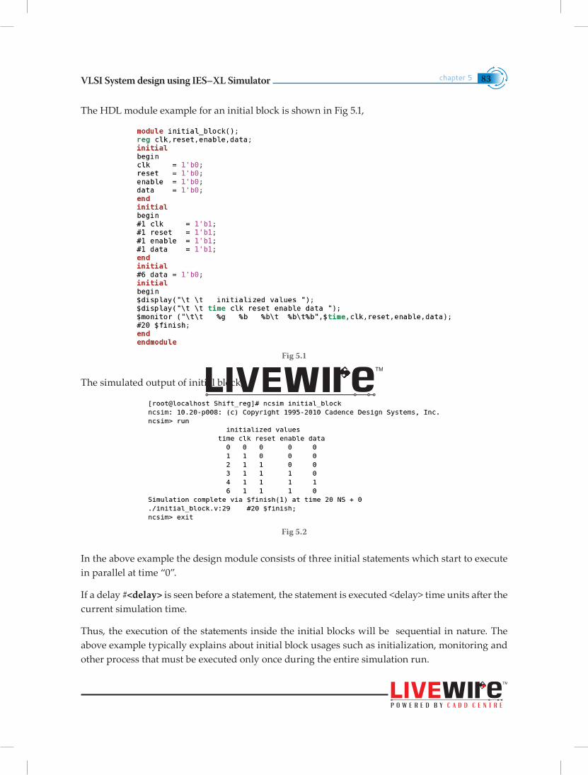
The HDL module example for an initial block is shown in Fig 5.1,
Fig 5.1
The simulated output of initial block,
Fig 5.2
In the above example the design module consists of three initial statements which start to execute in parallel at time “0”.
If a delay #<delay> is seen before a statement, the statement is executed <delay> time units after the current simulation time.
Thus, the execution of the statements inside the initial blocks will be sequential in nature. The above example typically explains about initial block usages such as initialization, monitoring and other process that must be executed only once during the entire simulation run.
VLSI System design using IES–XL Simulatorchapter 584
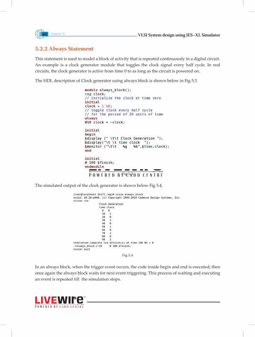
5.2.2 Always Statement
This statement is used to model a block of activity that is repeated continuously in a digital circuit. An example is a clock generator module that toggles the clock signal every half cycle. In real circuits, the clock generator is active from time 0 to as long as the circuit is powered on.
The HDL description of Clock generator using always block is shown below in Fig 5.3
Fig 5.3
The simulated output of the clock generator is shown below Fig 5.4,
Fig 5.4
In an always block, when the trigger event occurs, the code inside begin and end is executed; then once again the always block waits for next event triggering. This process of waiting and executing an event is repeated till the simulation stops.
VLSI System design using IES–XL Simulator chapter 5 85
In the above example the always statement starts at time “0” and executes the statement “clock = ~ clock” every 10 time units. Initialization of the clock has to be done inside a separate initial statement.
Once the initialization of clock has been done inside the always block, the clock will be initialized every time the “always” is entered. The simulation must be halted inside an initial statement. If there is no “$stop” or “$finish” statement to halt the simulation, the clock generator will be running forever.
The “always” block is used to model both the synchronous & combinational logic.
5.3 Procedural AssignmentsProcedural assignments update values of reg, integer, real or time variables. The syntax of the procedural assignment statement is shown below,
<assignment> :: = <value> = <expression>
Procedural statement <value> can be one of the following,
• A reg, integer, real or time register variable or a memory element.
• A bit select of these variables (e.g., adder [0])
• A part select of these variables (e.g., adder[15 : 10]
• A concatenation of any of the above.
For procedural assignments to registers,
• If right hand side has more bits than the register variable, the right hand side is truncated to match the width of the register variable.
• Least significant bits are selected and the most significant bits are discarded
• If the right hand side has fewer bits, zeros are filled in the most significant bits of the register variable.
There are two types of procedural assignments
• Blocking statements
• Non blocking statements
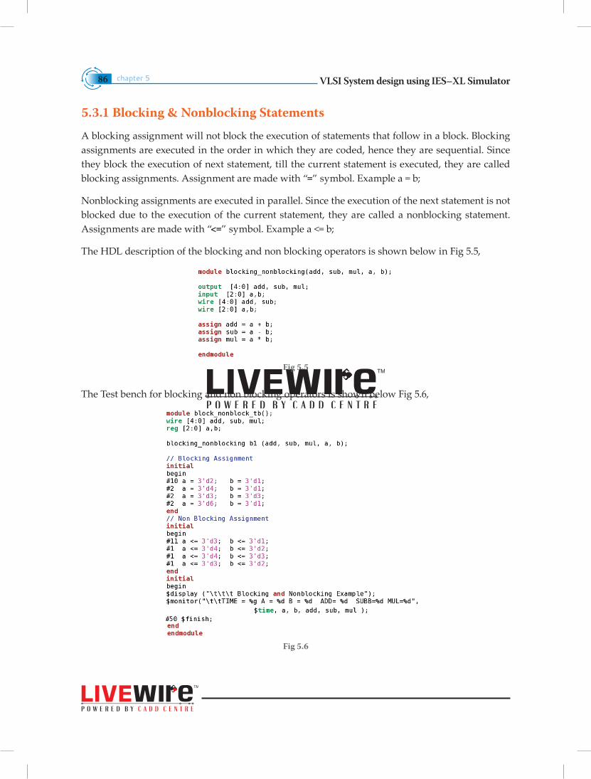
VLSI System design using IES–XL Simulatorchapter 586
5.3.1 Blocking & Nonblocking Statements
A blocking assignment will not block the execution of statements that follow in a block. Blocking assignments are executed in the order in which they are coded, hence they are sequential. Since they block the execution of next statement, till the current statement is executed, they are called blocking assignments. Assignment are made with “=” symbol. Example a = b;
Nonblocking assignments are executed in parallel. Since the execution of the next statement is not blocked due to the execution of the current statement, they are called a nonblocking statement. Assignments are made with “<=” symbol. Example a <= b;
The HDL description of the blocking and non blocking operators is shown below in Fig 5.5,
Fig 5.5
The Test bench for blocking and non blocking operators is shown below Fig 5.6,
Fig 5.6
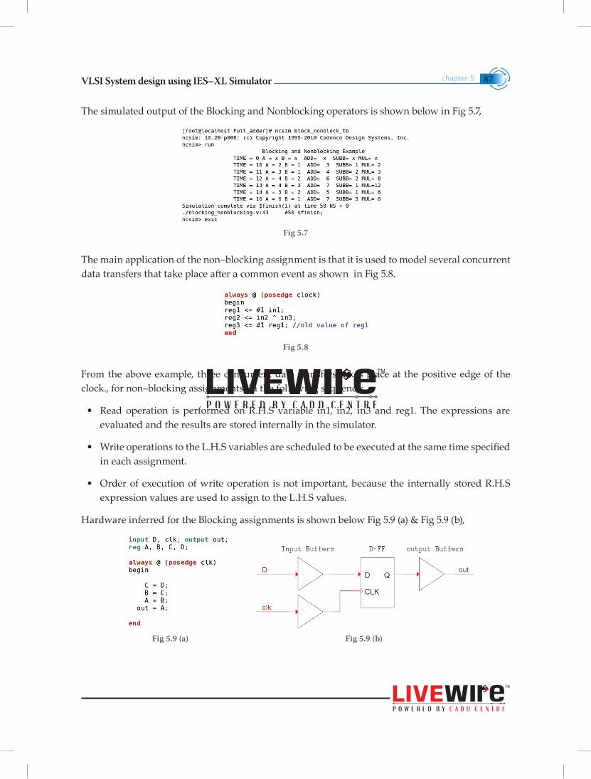
VLSI System design using IES–XL Simulator chapter 5 87
The simulated output of the Blocking and Nonblocking operators is shown below in Fig 5.7,
Fig 5.7
The main application of the non–blocking assignment is that it is used to model several concurrent data transfers that take place after a common event as shown in Fig 5.8.
Fig 5.8
From the above example, three concurrent data transfers takes place at the positive edge of the clock., for non–blocking assignments, in the following sequence:
• Read operation is performed on R.H.S variable in1, in2, in3 and reg1. The expressions are evaluated and the results are stored internally in the simulator.
• Write operations to the L.H.S variables are scheduled to be executed at the same time specified in each assignment.
• Order of execution of write operation is not important, because the internally stored R.H.S expression values are used to assign to the L.H.S values.
Hardware inferred for the Blocking assignments is shown below Fig 5.9 (a) & Fig 5.9 (b),
Fig 5.9 (a) Fig 5.9 (b)
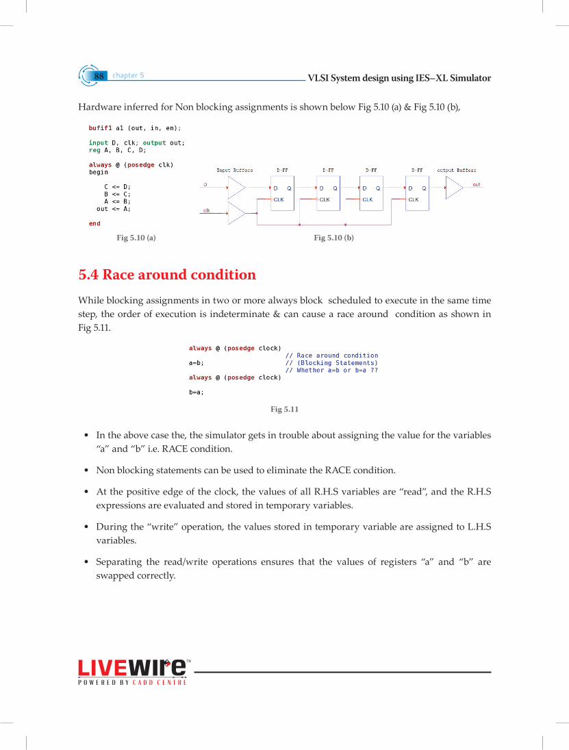
VLSI System design using IES–XL Simulatorchapter 588
Hardware inferred for Non blocking assignments is shown below Fig 5.10 (a) & Fig 5.10 (b),
Fig 5.10 (a) Fig 5.10 (b)
5.4 Race around conditionWhile blocking assignments in two or more always block scheduled to execute in the same time step, the order of execution is indeterminate & can cause a race around condition as shown in Fig 5.11.
Fig 5.11
• In the above case the, the simulator gets in trouble about assigning the value for the variables “a” and “b” i.e. RACE condition.
• Non blocking statements can be used to eliminate the RACE condition.
• At the positive edge of the clock, the values of all R.H.S variables are “read”, and the R.H.S expressions are evaluated and stored in temporary variables.
• During the “write” operation, the values stored in temporary variable are assigned to L.H.S variables.
• Separating the read/write operations ensures that the values of registers “a” and “b” are swapped correctly.
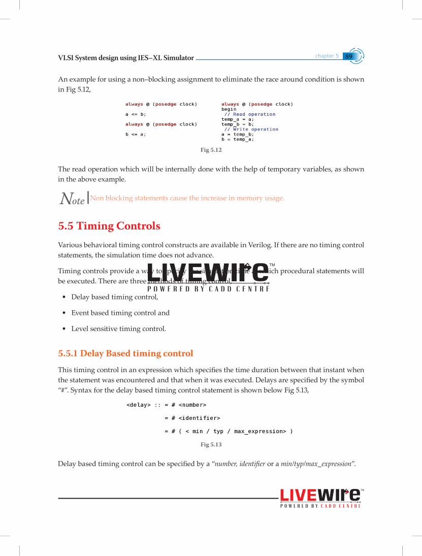
VLSI System design using IES–XL Simulator chapter 5 89
An example for using a non–blocking assignment to eliminate the race around condition is shown in Fig 5.12,
Fig 5.12
The read operation which will be internally done with the help of temporary variables, as shown in the above example.
Note Non blocking statements cause the increase in memory usage.
5.5 Timing ControlsVarious behavioral timing control constructs are available in Verilog. If there are no timing control statements, the simulation time does not advance.
Timing controls provide a way to specify the simulation time at which procedural statements will be executed. There are three methods of timing control,
• Delay based timing control,
• Event based timing control and
• Level sensitive timing control.
5.5.1 Delay Based timing control
This timing control in an expression which specifies the time duration between that instant when the statement was encountered and that when it was executed. Delays are specified by the symbol “#”. Syntax for the delay based timing control statement is shown below Fig 5.13,
Fig 5.13
Delay based timing control can be specified by a “number, identifier or a min/typ/max_expression”.
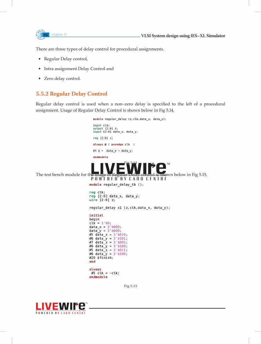
VLSI System design using IES–XL Simulatorchapter 590
There are three types of delay control for procedural assignments.
• Regular Delay control,
• Intra assignment Delay Control and
• Zero delay control.
5.5.2 Regular Delay Control
Regular delay control is used when a non–zero delay is specified to the left of a procedural assignment. Usage of Regular Delay Control is shown below in Fig 5.14,
Fig 5.14
The test bench module for the usage of Regular Delay control is shown below in Fig 5.15,
Fig 5.15
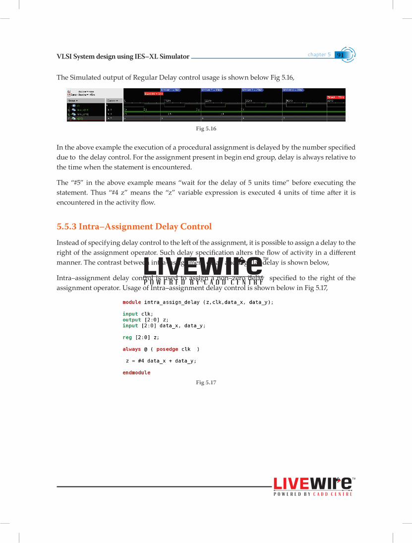
VLSI System design using IES–XL Simulator chapter 5 91
The Simulated output of Regular Delay control usage is shown below Fig 5.16,
Fig 5.16
In the above example the execution of a procedural assignment is delayed by the number specified due to the delay control. For the assignment present in begin end group, delay is always relative to the time when the statement is encountered.
The “#5” in the above example means “wait for the delay of 5 units time” before executing the statement. Thus “#4 z” means the “z” variable expression is executed 4 units of time after it is encountered in the activity flow.
5.5.3 Intra–Assignment Delay Control
Instead of specifying delay control to the left of the assignment, it is possible to assign a delay to the right of the assignment operator. Such delay specification alters the flow of activity in a different manner. The contrast between intra–assignment delay and regular delay is shown below,
Intra–assignment delay control is used to assign a non–zero delay specified to the right of the assignment operator. Usage of Intra–assignment delay control is shown below in Fig 5.17,
Fig 5.17
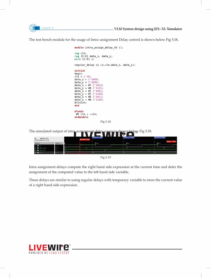
VLSI System design using IES–XL Simulatorchapter 592
The test bench module for the usage of Intra–assignment Delay control is shown below Fig 5.18,
Fig 5.18
The simulated output of intra assignment delay usage is shown below Fig 5.19,
Fig 5.19
Intra assignment delays compute the right hand side expression at the current time and defer the assignment of the computed value to the left hand side variable.
These delays are similar to using regular delays with temporary variable to store the current value of a right hand side expression.
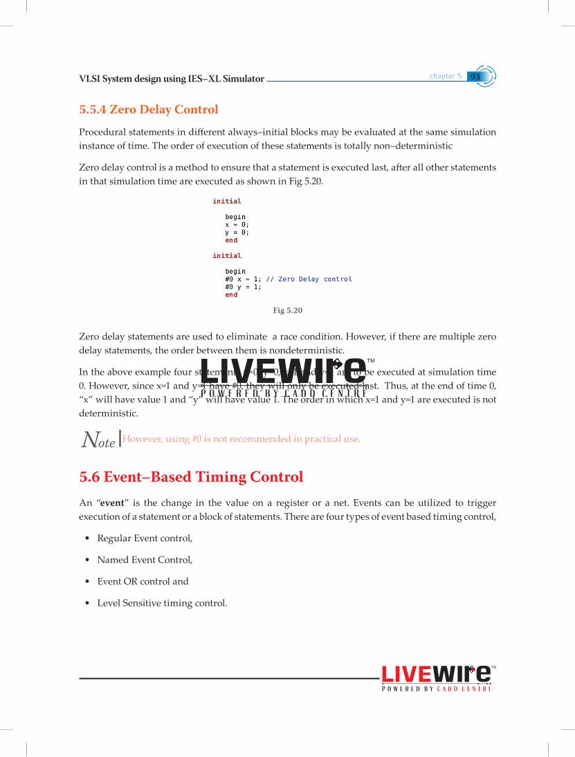
VLSI System design using IES–XL Simulator chapter 5 93
5.5.4 Zero Delay Control
Procedural statements in different always–initial blocks may be evaluated at the same simulation instance of time. The order of execution of these statements is totally non–deterministic
Zero delay control is a method to ensure that a statement is executed last, after all other statements in that simulation time are executed as shown in Fig 5.20.
Fig 5.20
Zero delay statements are used to eliminate a race condition. However, if there are multiple zero delay statements, the order between them is nondeterministic.
In the above example four statements x=0, y=0, x=1 and y=1 are to be executed at simulation time 0. However, since x=1 and y=1 have #0, they will only be executed last. Thus, at the end of time 0, “x” will have value 1 and “y” will have value 1. The order in which x=1 and y=1 are executed is not deterministic.
Note However, using #0 is not recommended in practical use.
5.6 Event–Based Timing ControlAn “event” is the change in the value on a register or a net. Events can be utilized to trigger execution of a statement or a block of statements. There are four types of event based timing control,
• Regular Event control,
• Named Event Control,
• Event OR control and
• Level Sensitive timing control.
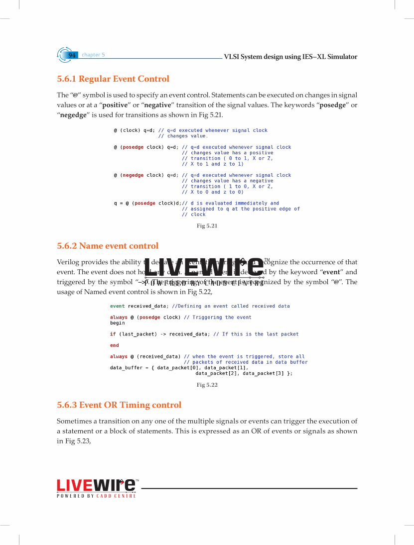
VLSI System design using IES–XL Simulatorchapter 594
5.6.1 Regular Event Control
The “@” symbol is used to specify an event control. Statements can be executed on changes in signal values or at a “positive” or “negative” transition of the signal values. The keywords “posedge” or “negedge” is used for transitions as shown in Fig 5.21.
Fig 5.21
5.6.2 Name event control
Verilog provides the ability to declare an event, then trigger and recognize the occurrence of that event. The event does not hold any data. A named event is declared by the keyword “event” and triggered by the symbol “–>”. The triggering of the event is recognized by the symbol “@”. The usage of Named event control is shown in Fig 5.22,
Fig 5.22
5.6.3 Event OR Timing control
Sometimes a transition on any one of the multiple signals or events can trigger the execution of a statement or a block of statements. This is expressed as an OR of events or signals as shown in Fig 5.23,
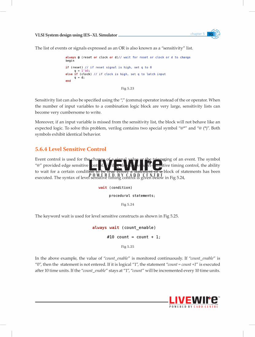
VLSI System design using IES–XL Simulator chapter 5 95
The list of events or signals expressed as an OR is also known as a “sensitivity” list.
Fig 5.23
Sensitivity list can also be specified using the “,” (comma) operator instead of the or operator. When the number of input variables to a combination logic block are very large, sensitivity lists can become very cumbersome to write.
Moreover, if an input variable is missed from the sensitivity list, the block will not behave like an expected logic. To solve this problem, verilog contains two special symbol “@*” and “@ (*)”. Both symbols exhibit identical behavior.
5.6.4 Level Sensitive Control
Event control is used for the change of a signal value or the triggering of an event. The symbol “@” provided edge sensitive control. Verilog also allows level–sensitive timing control, the ability to wait for a certain condition to be true before a statement or a block of statements has been executed. The syntax of level sensitive timing control is given below in Fig 5.24,
Fig 5.24
The keyword wait is used for level sensitive constructs as shown in Fig 5.25.
Fig 5.25
In the above example, the value of “count_enable” is monitored continuously. If “count_enable” is “0”, then the statement is not entered. If it is logical “1”, the statement “count = count +1” is executed after 10 time units. If the “count_enable” stays at “1”, “count” will be incremented every 10 time units.
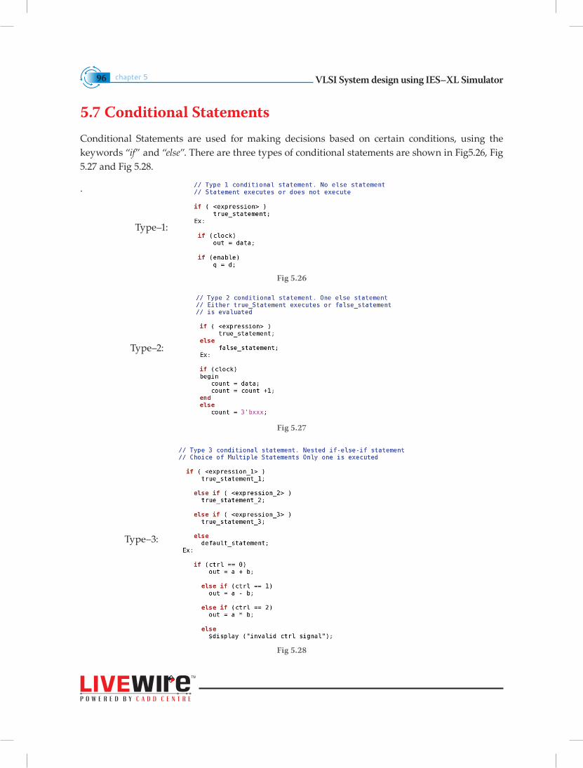
VLSI System design using IES–XL Simulatorchapter 596
5.7 Conditional StatementsConditional Statements are used for making decisions based on certain conditions, using the keywords “if” and “else”. There are three types of conditional statements are shown in Fig5.26, Fig 5.27 and Fig 5.28.
.
Fig 5.26
Fig 5.27
Fig 5.28
Type–1:
Type–2:
Type–3:
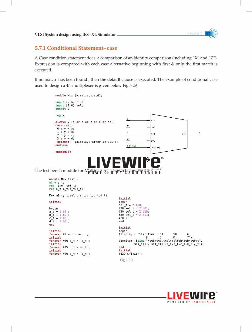
VLSI System design using IES–XL Simulator chapter 5 97
5.7.1 Conditional Statement–case
A Case condition statement does a comparison of an identity comparison (including “X” and “Z”). Expression is compared with each case alternative beginning with first & only the first match is executed.
If no match has been found , then the default clause is executed. The example of conditional case used to design a 4:1 multiplexer is given below Fig 5.29,
Fig 5.29
The test bench module for Multiplexer is shown below Fig 5.30,
Fig 5.30

VLSI System design using IES–XL Simulatorchapter 598
The Output of 4:1 Mux using conditional statement is shown below Fig 5.31,
Fig 5.31
When the sample input is checked under each conditions case, it appears as a simpler alternative
to “if” statement. Output must be explicitly or implicitly defined for all possible values of the case
expression to avoid undefined values.
Default output can be described either before the case statement with a variable assignment or in
case statement with a default clause.
Note Case statement in Verilog also generates a prioritized encoded hardware logic.
5.7.2 Case Variation–casex, casez
There are two variations of the case statement. They are denoted by keywords, casex and casez.
casex: Special version of a case in which “z” or “x” logic values in the case item or case expression
are considered to be don’t cares.
casez: Special version of case in which “z” logic values in the case item are treated as don’t cares.
Only one bit is considered to determine the next state whereas the other bits are ignored.
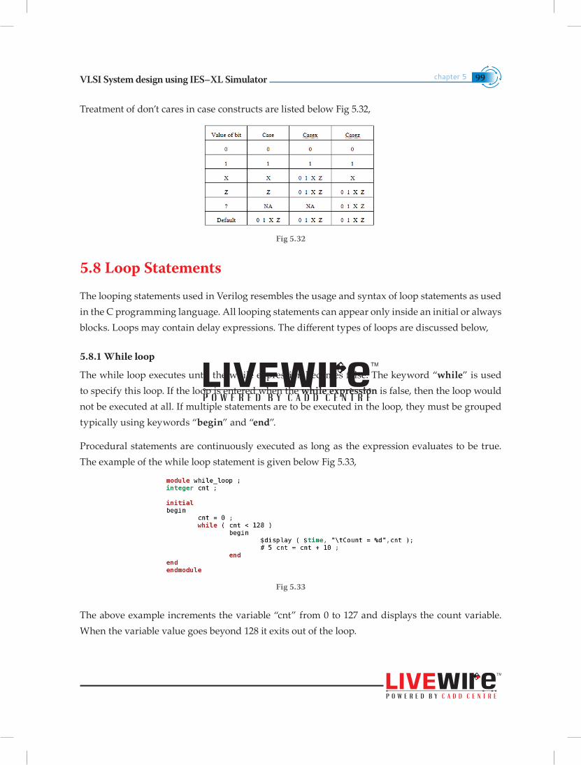
VLSI System design using IES–XL Simulator chapter 5 99
Treatment of don’t cares in case constructs are listed below Fig 5.32,
Fig 5.32
5.8 Loop Statements
The looping statements used in Verilog resembles the usage and syntax of loop statements as used in the C programming language. All looping statements can appear only inside an initial or always blocks. Loops may contain delay expressions. The different types of loops are discussed below,
5.8.1 While loop
The while loop executes until the while expression becomes false. The keyword “while” is used to specify this loop. If the loop is entered when the while expression is false, then the loop would not be executed at all. If multiple statements are to be executed in the loop, they must be grouped typically using keywords “begin” and “end”.
Procedural statements are continuously executed as long as the expression evaluates to be true. The example of the while loop statement is given below Fig 5.33,
Fig 5.33
The above example increments the variable “cnt” from 0 to 127 and displays the count variable. When the variable value goes beyond 128 it exits out of the loop.
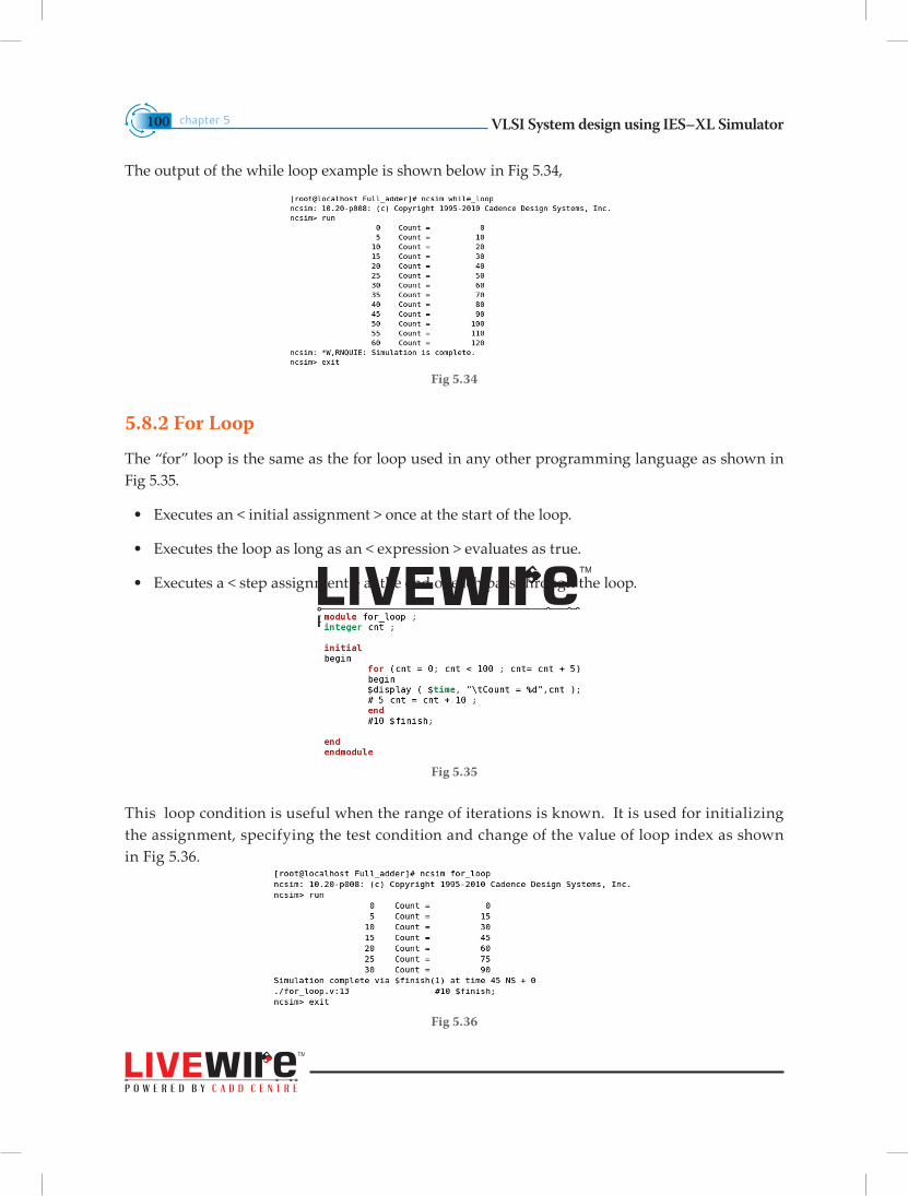
VLSI System design using IES–XL Simulatorchapter 5100
The output of the while loop example is shown below in Fig 5.34,
Fig 5.34
5.8.2 For Loop
The “for” loop is the same as the for loop used in any other programming language as shown in Fig 5.35.
• Executes an < initial assignment > once at the start of the loop.
• Executes the loop as long as an < expression > evaluates as true.
• Executes a < step assignment > at the end of each pass through the loop.
Fig 5.35
This loop condition is useful when the range of iterations is known. It is used for initializing the assignment, specifying the test condition and change of the value of loop index as shown in Fig 5.36.
Fig 5.36
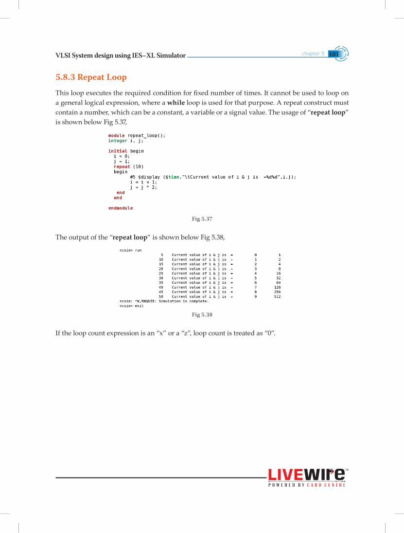
VLSI System design using IES–XL Simulator chapter 5 101
5.8.3 Repeat Loop
This loop executes the required condition for fixed number of times. It cannot be used to loop on a general logical expression, where a while loop is used for that purpose. A repeat construct must contain a number, which can be a constant, a variable or a signal value. The usage of “repeat loop” is shown below Fig 5.37,
Fig 5.37
The output of the “repeat loop” is shown below Fig 5.38,
Fig 5.38
If the loop count expression is an “x” or a “z”, loop count is treated as “0”.
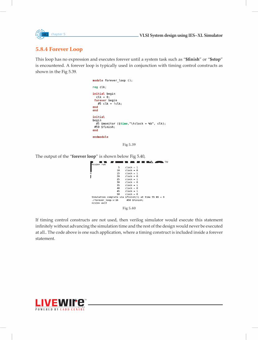
VLSI System design using IES–XL Simulatorchapter 5102
5.8.4 Forever Loop
This loop has no expression and executes forever until a system task such as “$finish” or “$stop” is encountered. A forever loop is typically used in conjunction with timing control constructs as shown in the Fig 5.39.
Fig 5.39
The output of the “forever loop” is shown below Fig 5.40,
Fig 5.40
If timing control constructs are not used, then verilog simulator would execute this statement infinitely without advancing the simulation time and the rest of the design would never be executed at all.. The code above is one such application, where a timing construct is included inside a forever statement.
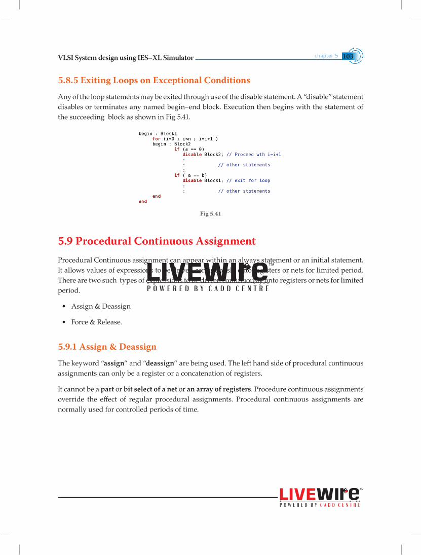
VLSI System design using IES–XL Simulator chapter 5 103
5.8.5 Exiting Loops on Exceptional Conditions
Any of the loop statements may be exited through use of the disable statement. A “disable” statement disables or terminates any named begin–end block. Execution then begins with the statement of the succeeding block as shown in Fig 5.41.
Fig 5.41
5.9 Procedural Continuous AssignmentProcedural Continuous assignment can appear within an always statement or an initial statement. It allows values of expressions to be driven continuously onto registers or nets for limited period. There are two such types of expressions to be driven continuously onto registers or nets for limited period.
• Assign & Deassign
• Force & Release.
5.9.1 Assign & Deassign
The keyword “assign” and “deassign” are being used. The left hand side of procedural continuous assignments can only be a register or a concatenation of registers.
It cannot be a part or bit select of a net or an array of registers. Procedure continuous assignments override the effect of regular procedural assignments. Procedural continuous assignments are normally used for controlled periods of time.
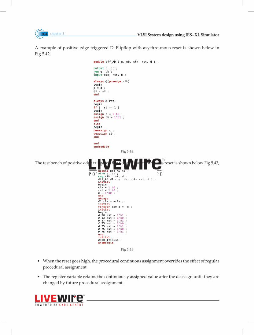
VLSI System design using IES–XL Simulatorchapter 5104
A example of positive edge triggered D–Flipflop with asychrounous reset is shown below in Fig 5.42,
Fig 5.42
The test bench of positive edge triggered flip flop with asynchronous reset is shown below Fig 5.43,
Fig 5.43
• When the reset goes high, the procedural continuous assignment overrides the effect of regular procedural assignment.
• The register variable retains the continuously assigned value after the deassign until they are changed by future procedural assignment.
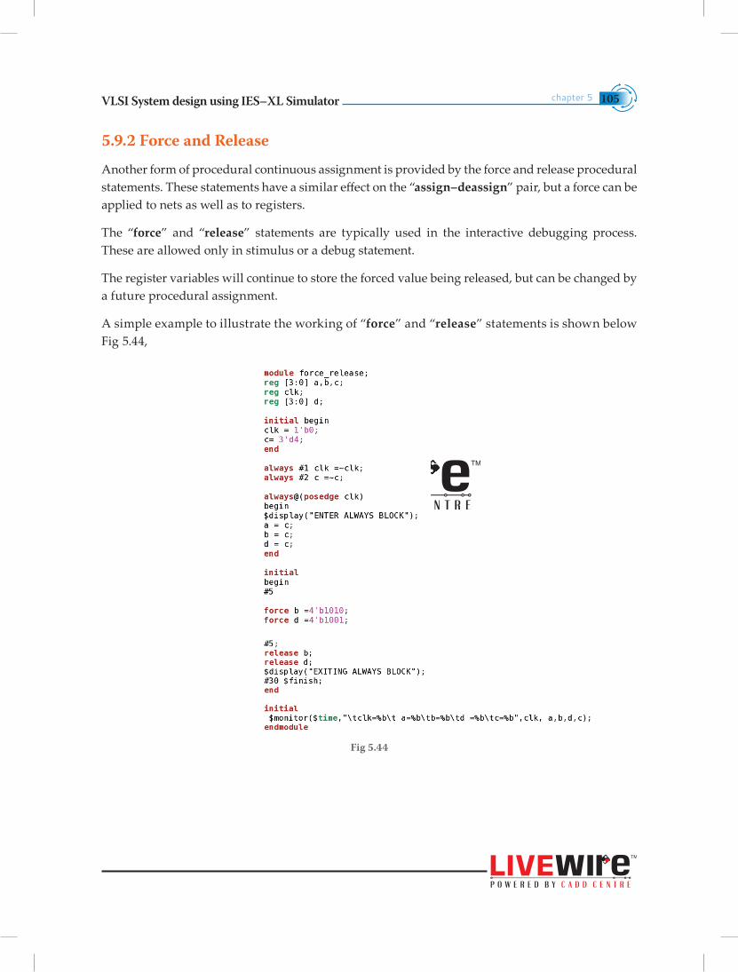
VLSI System design using IES–XL Simulator chapter 5 105
5.9.2 Force and Release
Another form of procedural continuous assignment is provided by the force and release procedural statements. These statements have a similar effect on the “assign–deassign” pair, but a force can be applied to nets as well as to registers.
The “force” and “release” statements are typically used in the interactive debugging process. These are allowed only in stimulus or a debug statement.
The register variables will continue to store the forced value being released, but can be changed by a future procedural assignment.
A simple example to illustrate the working of “force” and “release” statements is shown below Fig 5.44,
Fig 5.44
VLSI System design using IES–XL Simulatorchapter 5106
The response of the force and release statements shown as below in Fig 5.45,
Fig 5.45
Note Force and Release statements cannot be used inside design blocks.
5.10 Sequential and Parallel BlocksBlock statements are used to group multiple statements to act together as one. In previous cases we have used keywords like “begin” and “end” to group multiple statements. In order to execute the statements to be executed in sequential or parallel we need to use two types of blocks,
• “sequential” blocks and
• “parallel” blocks.
5.10.1 Sequential blocks
This block is used where the statements in the block execute one after another. The keywords “begin” and “end” is used to group statements into sequential blocks.
The characteristics of Sequential Blocks are,
• The statements in a sequential block are processed in the order they are specified. A statement is executed only after its preceding statement completes the execution (except for non blocking assignments with intra assignment timing control).
• If the delay or event control is specified, it is relative to the simulation time when the previous statement in the block completed execution.
• Block finishes after the last statement in the block is executed.
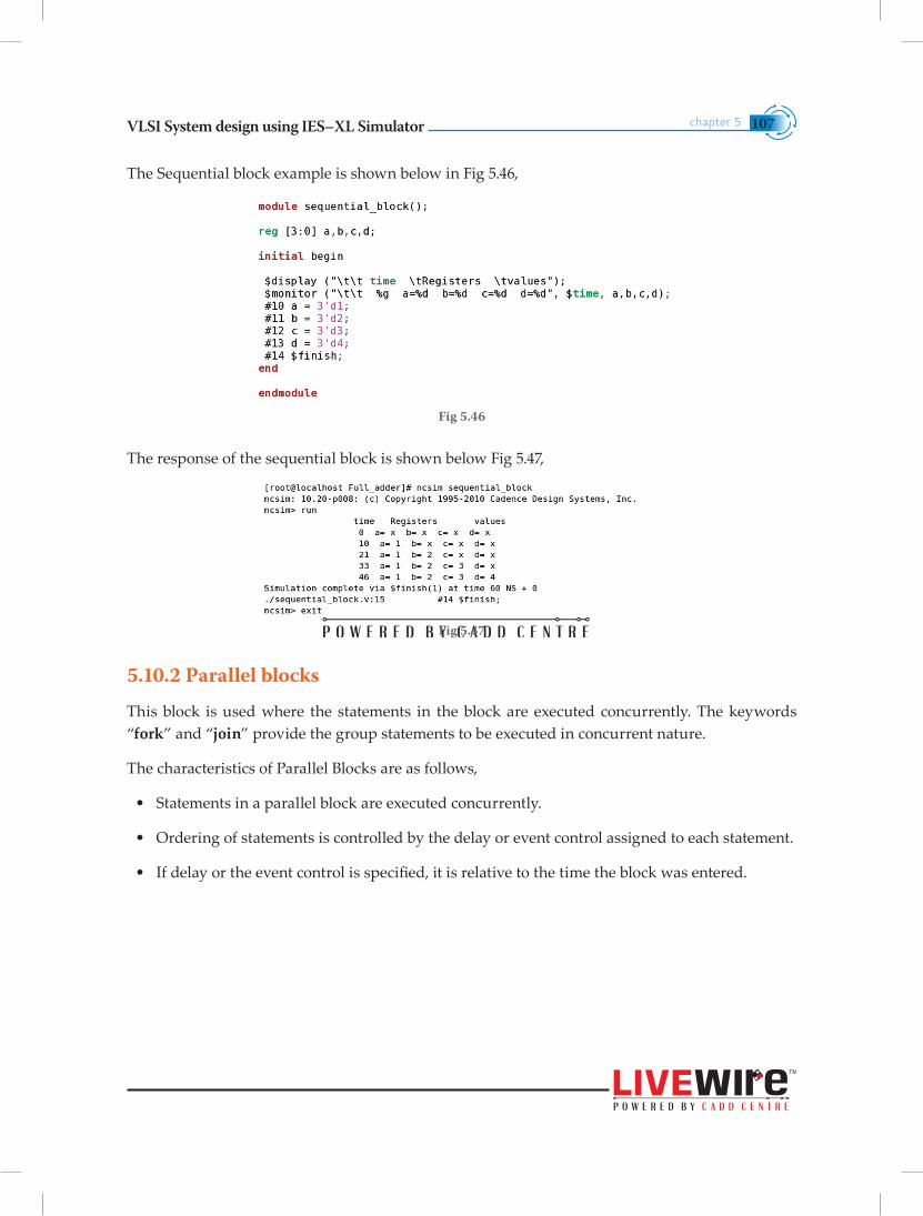
VLSI System design using IES–XL Simulator chapter 5 107
The Sequential block example is shown below in Fig 5.46,
Fig 5.46
The response of the sequential block is shown below Fig 5.47,
Fig 5.47
5.10.2 Parallel blocks
This block is used where the statements in the block are executed concurrently. The keywords “fork” and “join” provide the group statements to be executed in concurrent nature.
The characteristics of Parallel Blocks are as follows,
• Statements in a parallel block are executed concurrently.
• Ordering of statements is controlled by the delay or event control assigned to each statement.
• If delay or the event control is specified, it is relative to the time the block was entered.
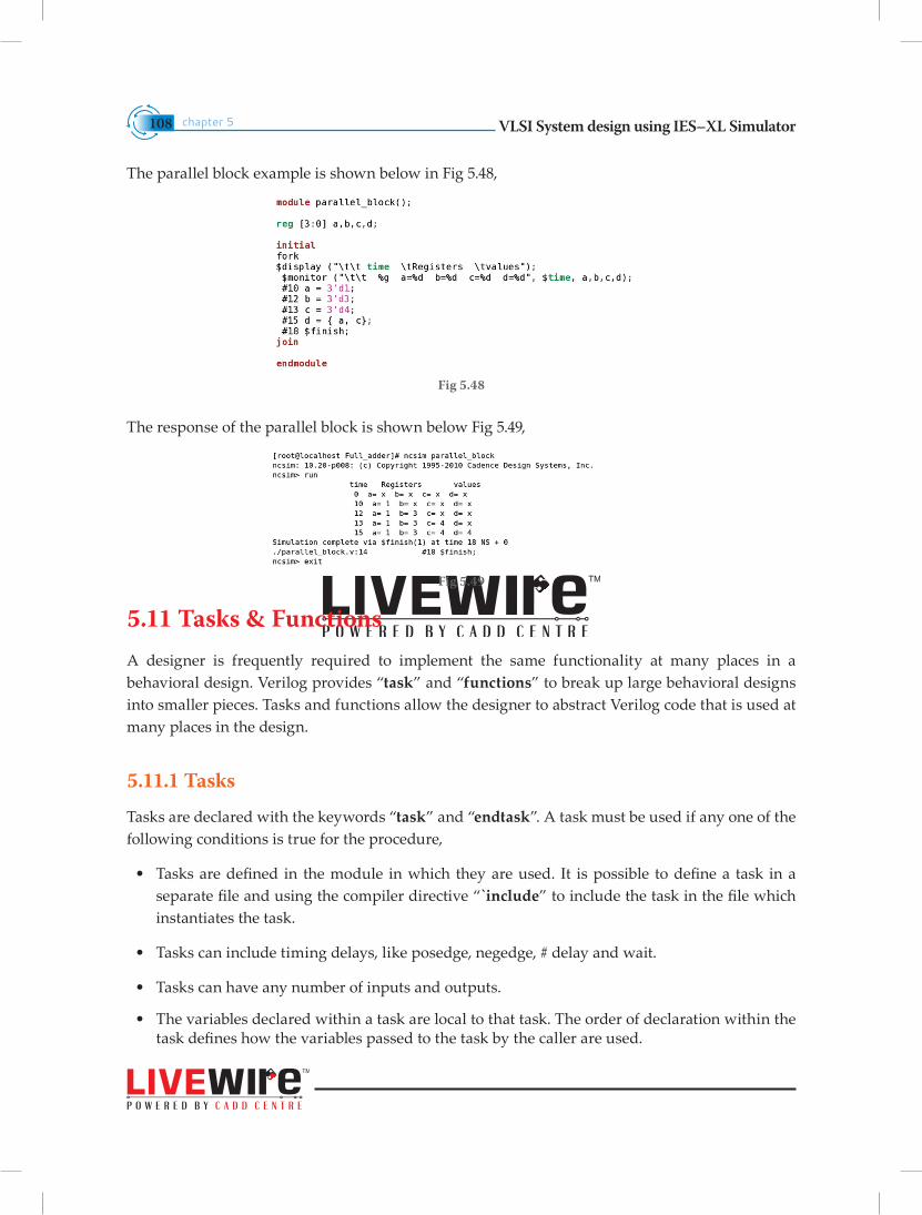
VLSI System design using IES–XL Simulatorchapter 5108
The parallel block example is shown below in Fig 5.48,
Fig 5.48
The response of the parallel block is shown below Fig 5.49,
Fig 5.49
5.11 Tasks & FunctionsA designer is frequently required to implement the same functionality at many places in a behavioral design. Verilog provides “task” and “functions” to break up large behavioral designs into smaller pieces. Tasks and functions allow the designer to abstract Verilog code that is used at many places in the design.
5.11.1 Tasks
Tasks are declared with the keywords “task” and “endtask”. A task must be used if any one of the following conditions is true for the procedure,
• Tasks are defined in the module in which they are used. It is possible to define a task in a separate file and using the compiler directive “`include” to include the task in the file which instantiates the task.
• Tasks can include timing delays, like posedge, negedge, # delay and wait.
• Tasks can have any number of inputs and outputs.
• The variables declared within a task are local to that task. The order of declaration within the task defines how the variables passed to the task by the caller are used.
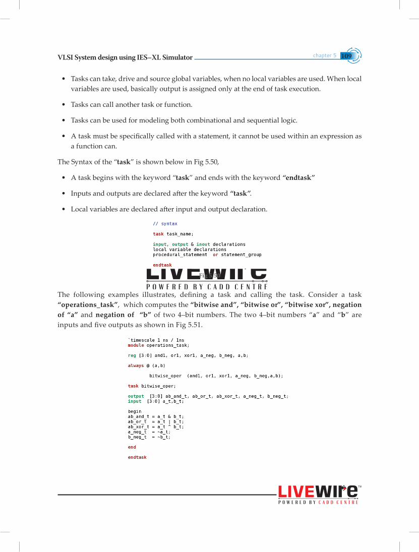
VLSI System design using IES–XL Simulator chapter 5 109
• Tasks can take, drive and source global variables, when no local variables are used. When local variables are used, basically output is assigned only at the end of task execution.
• Tasks can call another task or function.
• Tasks can be used for modeling both combinational and sequential logic.
• A task must be specifically called with a statement, it cannot be used within an expression as a function can.
The Syntax of the “task” is shown below in Fig 5.50,
• A task begins with the keyword “task” and ends with the keyword “endtask”
• Inputs and outputs are declared after the keyword “task”.
• Local variables are declared after input and output declaration.
Fig 5.50
The following examples illustrates, defining a task and calling the task. Consider a task “operations_task”, which computes the “bitwise and”, “bitwise or”, “bitwise xor”, negation of “a” and negation of “b” of two 4–bit numbers. The two 4–bit numbers “a” and “b” are inputs and five outputs as shown in Fig 5.51.
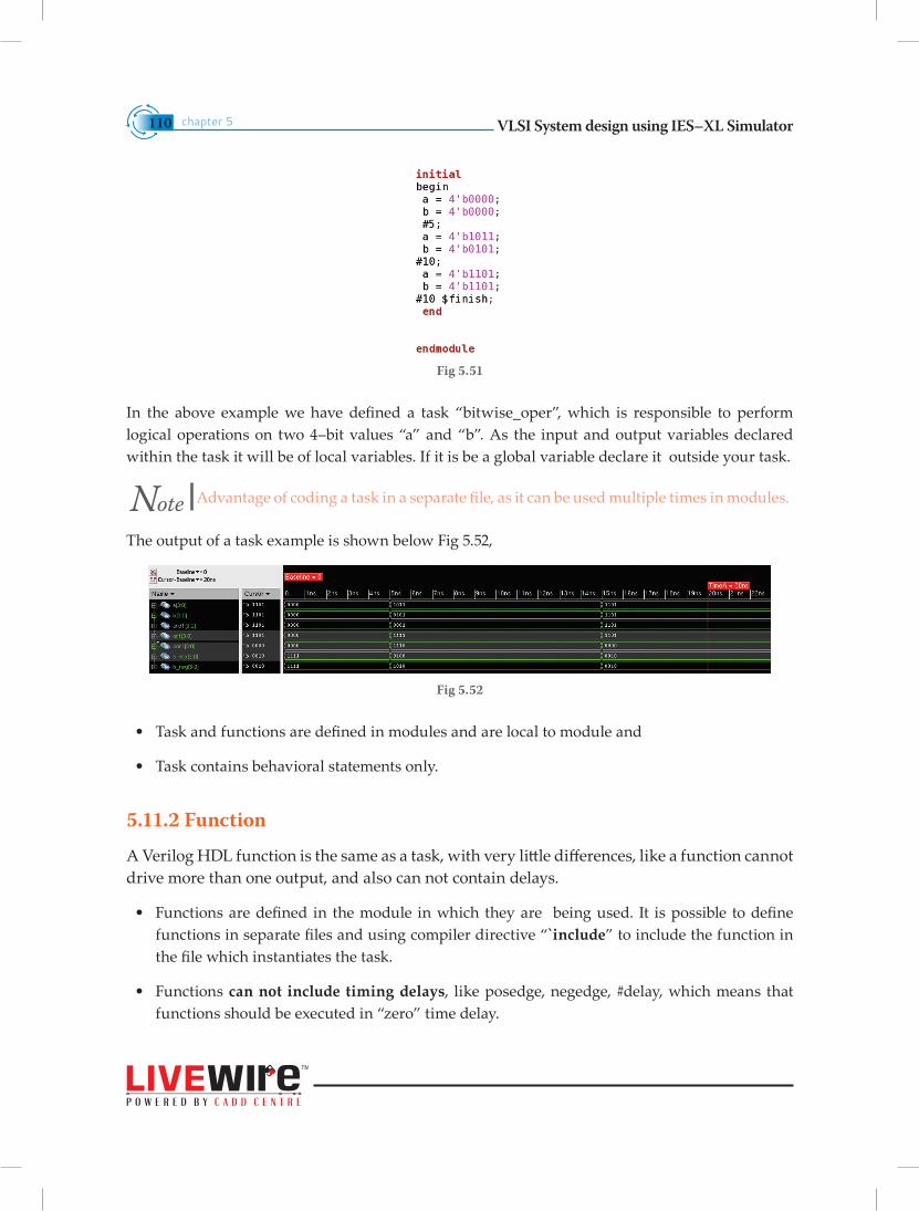
VLSI System design using IES–XL Simulatorchapter 5110
Fig 5.51
In the above example we have defined a task “bitwise_oper”, which is responsible to perform logical operations on two 4–bit values “a” and “b”. As the input and output variables declared within the task it will be of local variables. If it is be a global variable declare it outside your task.
Note Advantage of coding a task in a separate file, as it can be used multiple times in modules.
The output of a task example is shown below Fig 5.52,
Fig 5.52
• Task and functions are defined in modules and are local to module and
• Task contains behavioral statements only.
5.11.2 Function
A Verilog HDL function is the same as a task, with very little differences, like a function cannot drive more than one output, and also can not contain delays.
• Functions are defined in the module in which they are being used. It is possible to define functions in separate files and using compiler directive “`include” to include the function in the file which instantiates the task.
• Functions can not include timing delays, like posedge, negedge, #delay, which means that functions should be executed in “zero” time delay.
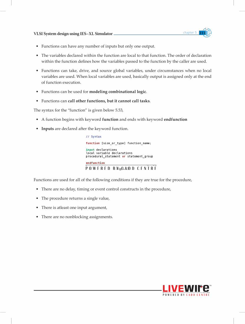
VLSI System design using IES–XL Simulator chapter 5 111
• Functions can have any number of inputs but only one output.
• The variables declared within the function are local to that function. The order of declaration within the function defines how the variables passed to the function by the caller are used.
• Functions can take, drive, and source global variables, under circumstances when no local variables are used. When local variables are used, basically output is assigned only at the end of function execution.
• Functions can be used for modeling combinational logic.
• Functions can call other functions, but it cannot call tasks.
The syntax for the “function” is given below 5.53,
• A function begins with keyword function and ends with keyword endfunction
• Inputs are declared after the keyword function.
Fig 5.53
Functions are used for all of the following conditions if they are true for the procedure,
• There are no delay, timing or event control constructs in the procedure,
• The procedure returns a single value,
• There is atleast one input argument,
• There are no nonblocking assignments.
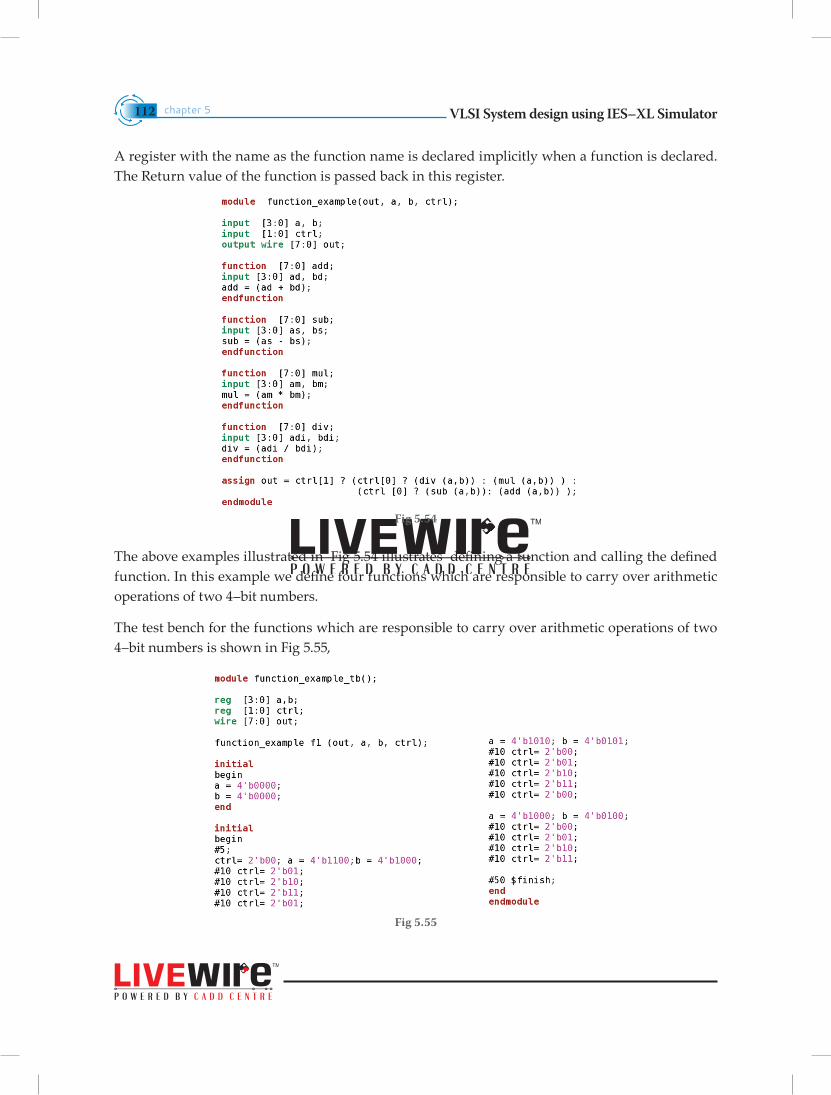
VLSI System design using IES–XL Simulatorchapter 5112
A register with the name as the function name is declared implicitly when a function is declared. The Return value of the function is passed back in this register.
Fig 5.54
The above examples illustrated in Fig 5.54 illustrates defining a function and calling the defined function. In this example we define four functions which are responsible to carry over arithmetic operations of two 4–bit numbers.
The test bench for the functions which are responsible to carry over arithmetic operations of two 4–bit numbers is shown in Fig 5.55,
Fig 5.55
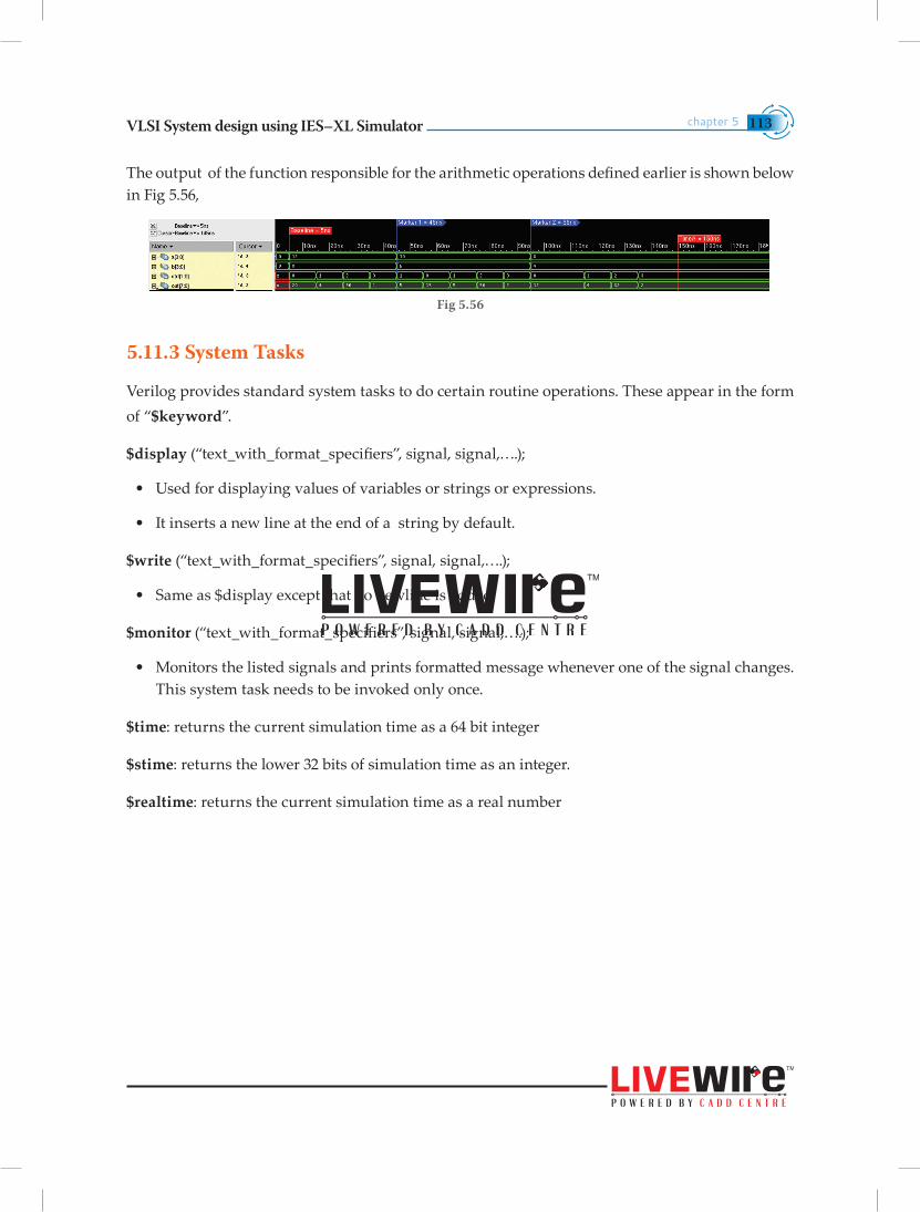
VLSI System design using IES–XL Simulator chapter 5 113
The output of the function responsible for the arithmetic operations defined earlier is shown below in Fig 5.56,
Fig 5.56
5.11.3 System Tasks
Verilog provides standard system tasks to do certain routine operations. These appear in the form of “$keyword”.
$display (“text_with_format_specifiers”, signal, signal,….);
• Used for displaying values of variables or strings or expressions.
• It inserts a new line at the end of a string by default.
$write (“text_with_format_specifiers”, signal, signal,….);
• Same as $display except that no newline is added.
$monitor (“text_with_format_specifiers”, signal, signal,….);
• Monitors the listed signals and prints formatted message whenever one of the signal changes. This system task needs to be invoked only once.
$time: returns the current simulation time as a 64 bit integer
$stime: returns the lower 32 bits of simulation time as an integer.
$realtime: returns the current simulation time as a real number
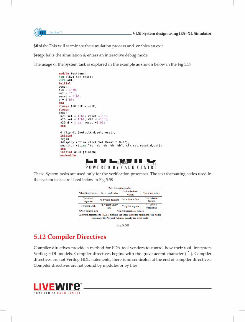
VLSI System design using IES–XL Simulatorchapter 5114
$finish: This will terminate the simulation process and enables an exit.
$stop: halts the simulation & enters an interactive debug mode.
The usage of the System task is explored in the example as shown below in the Fig 5.57
Fig 5.57
These System tasks are used only for the verification processes. The text formatting codes used in the system tasks are listed below in Fig 5.58
Fig 5.58
5.12 Compiler DirectivesCompiler directives provide a method for EDA tool vendors to control how their tool interprets Verilog HDL models. Compiler directives begins with the grave accent character ( ` ). Compiler directives are not Verilog HDL statements, there is no semicolon at the end of compiler directives. Compiler directives are not bound by modules or by files.
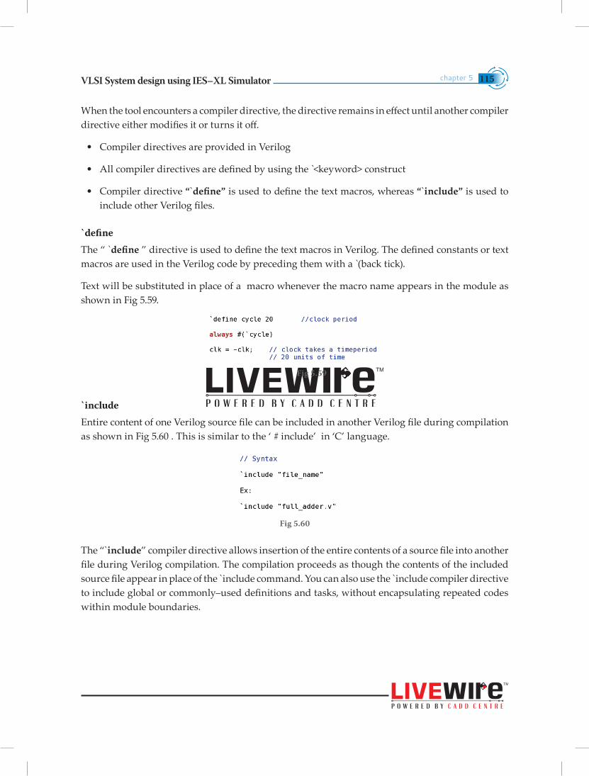
VLSI System design using IES–XL Simulator chapter 5 115
When the tool encounters a compiler directive, the directive remains in effect until another compiler directive either modifies it or turns it off.
• Compiler directives are provided in Verilog
• All compiler directives are defined by using the <̀keyword> construct
• Compiler directive “`define” is used to define the text macros, whereas “`include” is used to include other Verilog files.
`defineThe “ `define ” directive is used to define the text macros in Verilog. The defined constants or text macros are used in the Verilog code by preceding them with a (̀back tick).
Text will be substituted in place of a macro whenever the macro name appears in the module as shown in Fig 5.59.
Fig 5.59
`includeEntire content of one Verilog source file can be included in another Verilog file during compilation as shown in Fig 5.60 . This is similar to the ‘ # include’ in ‘C’ language.
Fig 5.60
The “`include” compiler directive allows insertion of the entire contents of a source file into another file during Verilog compilation. The compilation proceeds as though the contents of the included source file appear in place of the ̀ include command. You can also use the ̀ include compiler directive to include global or commonly–used definitions and tasks, without encapsulating repeated codes within module boundaries.
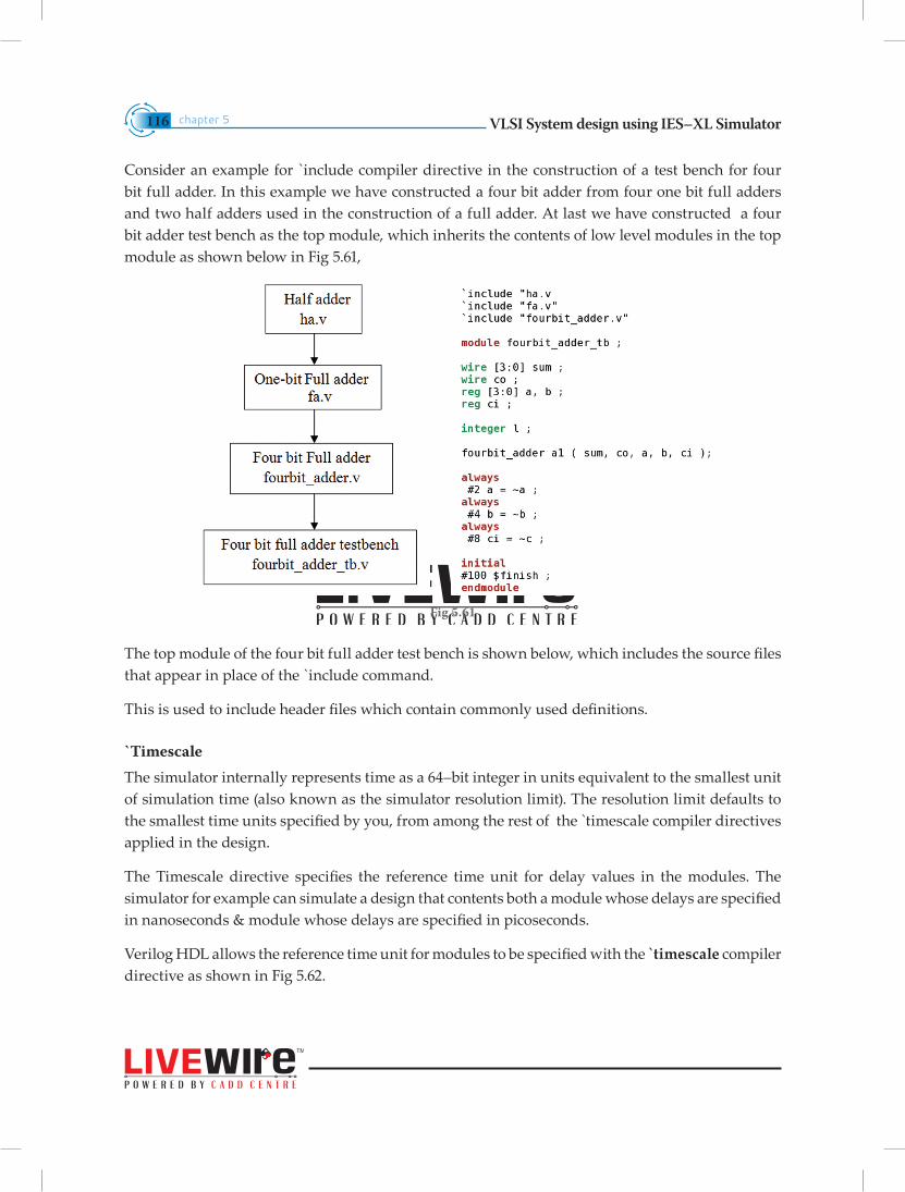
VLSI System design using IES–XL Simulatorchapter 5116
Consider an example for `include compiler directive in the construction of a test bench for four bit full adder. In this example we have constructed a four bit adder from four one bit full adders and two half adders used in the construction of a full adder. At last we have constructed a four bit adder test bench as the top module, which inherits the contents of low level modules in the top module as shown below in Fig 5.61,
Fig 5.61
The top module of the four bit full adder test bench is shown below, which includes the source files that appear in place of the `include command.
This is used to include header files which contain commonly used definitions.
`TimescaleThe simulator internally represents time as a 64–bit integer in units equivalent to the smallest unit of simulation time (also known as the simulator resolution limit). The resolution limit defaults to the smallest time units specified by you, from among the rest of the `timescale compiler directives applied in the design.
The Timescale directive specifies the reference time unit for delay values in the modules. The simulator for example can simulate a design that contents both a module whose delays are specified in nanoseconds & module whose delays are specified in picoseconds.
Verilog HDL allows the reference time unit for modules to be specified with the ̀ timescale compiler directive as shown in Fig 5.62.
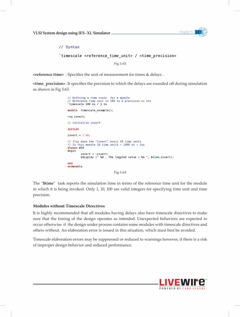
VLSI System design using IES–XL Simulator chapter 5 117
Fig 5.62
<reference time> : Specifies the unit of measurement for times & delays .
<time_precision> : It specifies the precision to which the delays are rounded off during simulation as shown in Fig 5.63.
Fig 5.63
The “$time” task reports the simulation time in terms of the reference time unit for the module in which it is being invoked. Only 1, 10, 100 are valid integers for specifying time unit and time precision.
Modules without Timescale Directives It is highly recommended that all modules having delays also have timescale directives to make sure that the timing of the design operates as intended. Unexpected behaviors are expected to occur otherwise if the design under process contains some modules with timescale directives and others without. An elaboration error is issued in this situation, which must best be avoided.
Timescale elaboration errors may be suppressed or reduced to warnings however, if there is a risk of improper design behavior and reduced performance.
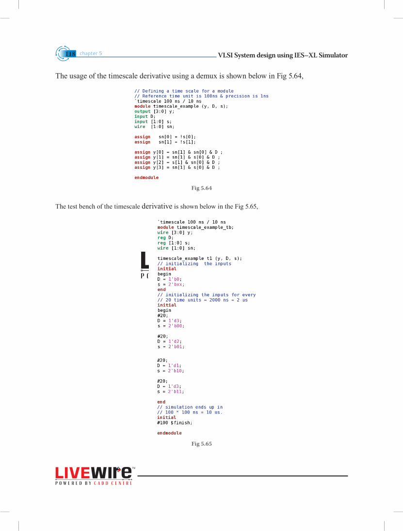
VLSI System design using IES–XL Simulatorchapter 5118
The usage of the timescale derivative using a demux is shown below in Fig 5.64,
Fig 5.64
The test bench of the timescale derivative is shown below in the Fig 5.65,
Fig 5.65
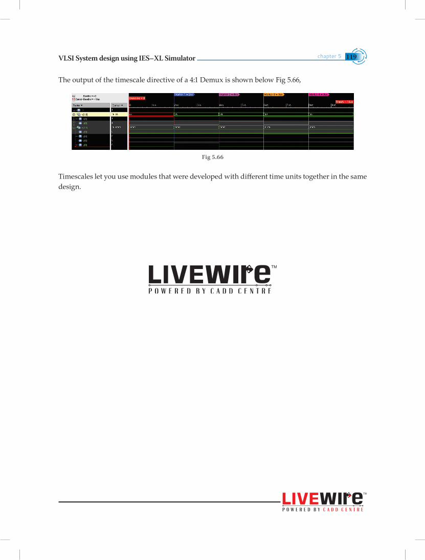
VLSI System design using IES–XL Simulator chapter 5 119
The output of the timescale directive of a 4:1 Demux is shown below Fig 5.66,
Fig 5.66
Timescales let you use modules that were developed with different time units together in the same design.
VLSI System design using IES–XL Simulatorchapter 5120
1. What do you mean by structured procedure always ?
2. What do you mean by structured procedure initial?
3. Differentiae blocking and non blocking statements?
4. What do you mean by race around condition and how it can be avoided using procedural statements?
5. What do you mean by timing control and what are the types of timing control?
6. How intra assignment Delay control is used?
7. Define Event based delay control and classify the types of Event control.
8. Explain assign and deassign statements.
9. Define force and release.
10. Differentiate between Sequential and Parallel block.
11. Differentiate between Task and Function.
12. What do you mean by system task and give some examples?
13. What do you mean by text formatting code?
14. Define compiler directive.
15. What do you mean by timescale?
This chapter
• Explains the significance of structured procedures always and initial in behavioral modeling
• Describes the usage of the blocking and nonblocking procedural assignments
• Enables the user to understand the delay based timing control mechanism in behavioral modeling.
• Describes the usage of conditional and looping statements.
Highlights
Questions

Self Assessment


VLSI System design using IES–XL Simulator Self Assessment 123
Self Assessment
1. Explain the typical design flow for designing VLSI IC circuit?
2. Describe the four levels of abstraction to represent a full substractor independently?
3. What do you mean by instantiation?
4. What is the purpose of stimulus block? How many styles of stimulus block application are possible.
5. Design a clock with the time period of 30 by using the always and initial statements. The value of clock at time = 0 should be initialized to ‘0’.
6. Using continuous assignment statements describe verilog description for a full adder. Use 5 units of delay for XOR gate and 3 units of time for AND & OR gate.
7. Design 4 to 1 multiplexer using if and else statements.
8. When to model a functionality as UDP ?
9. Define a function to calculate the factorial of a 3 bit number. The output is 4 bit value. Invoke the function by using stimulus and check results.
10. Write a truth table for the Boolean function Output = ((A|B)|(C&D)). Define a UDP that implements this Boolean function. Assume no input value ‘X’.
11. What do you mean by FSM?
12. What is the use of schematic tracer window?
13. What does source browser window does?
14. Differentiate Mealy and Moore Machine.
15. What does `timescale 1 ns/1 ps signify in a verilog code?
16. What is the difference between the following two lines of Verilog code?
#5 a = b; a = #5 b;
17. Design a 4–bit PRBS generator using LFSR in behavioural modeling.


Work Book

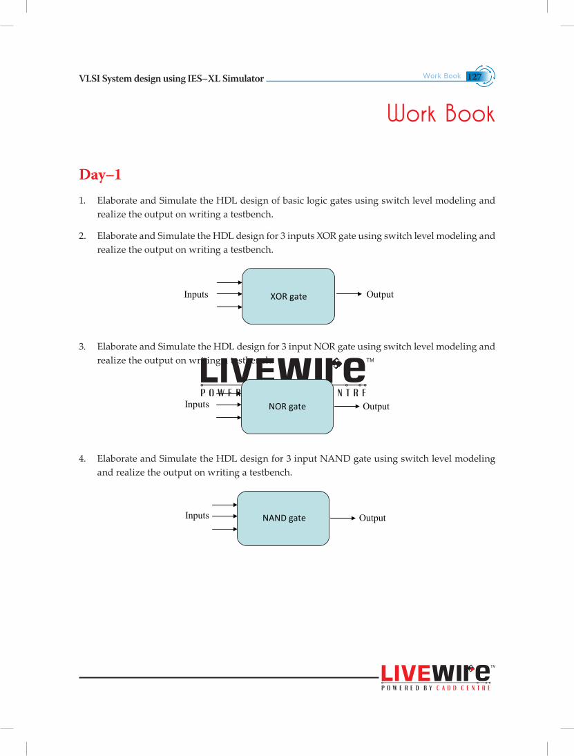
VLSI System design using IES–XL Simulator Work Book 127
Work Book
Day–1 1. Elaborate and Simulate the HDL design of basic logic gates using switch level modeling and
realize the output on writing a testbench.
2. Elaborate and Simulate the HDL design for 3 inputs XOR gate using switch level modeling and realize the output on writing a testbench.
3. Elaborate and Simulate the HDL design for 3 input NOR gate using switch level modeling and realize the output on writing a testbench.
4. Elaborate and Simulate the HDL design for 3 input NAND gate using switch level modeling and realize the output on writing a testbench.
XOR gate Inputs Output
NOR gate
Inputs Output
NAND gate
Inputs Output
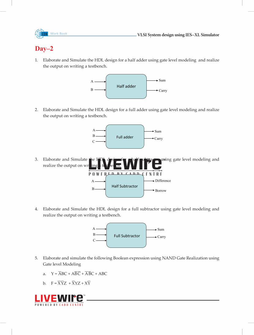
VLSI System design using IES–XL SimulatorWork Book128
Day–2 1. Elaborate and Simulate the HDL design for a half adder using gate level modeling and realize
the output on writing a testbench.
2. Elaborate and Simulate the HDL design for a full adder using gate level modeling and realize the output on writing a testbench.
3. Elaborate and Simulate the HDL design for a half subtractor using gate level modeling and realize the output on writing a testbench.
4. Elaborate and Simulate the HDL design for a full subtractor using gate level modeling and realize the output on writing a testbench.
5. Elaborate and simulate the following Boolean expression using NAND Gate Realization using Gate level Modeling
a. Y = ABC + AB C + A BC + ABC
b. F = X YZ + XYZ + XY
Half adder
A Sum
B
Carry
Full adder
A
Sum B
Carry C
Half Subtractor
A Difference
B Borrow
Full Subtractor
A Sum
B Carry
C
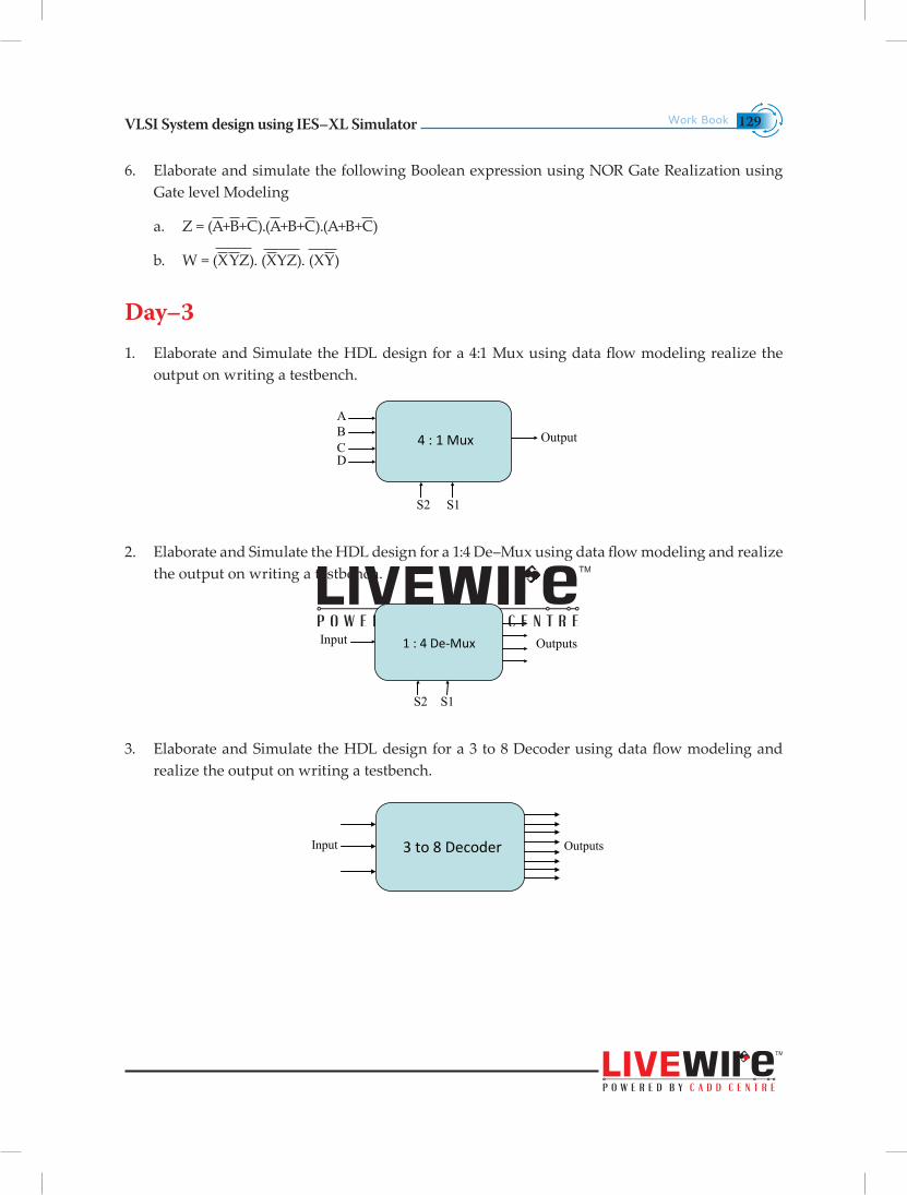
VLSI System design using IES–XL Simulator Work Book 129
6. Elaborate and simulate the following Boolean expression using NOR Gate Realization using Gate level Modeling
a. Z = (A+B+C).(A+B+C).(A+B+C)
b. W = (X YZ). (XYZ). (XY)
Day–31. Elaborate and Simulate the HDL design for a 4:1 Mux using data flow modeling realize the
output on writing a testbench.
2. Elaborate and Simulate the HDL design for a 1:4 De–Mux using data flow modeling and realize the output on writing a testbench.
3. Elaborate and Simulate the HDL design for a 3 to 8 Decoder using data flow modeling and realize the output on writing a testbench.
4 : 1 Mux
A
B
Output
C
D
S2 S1
1 : 4 De-Mux
Input Outputs
S2 S1
3 to 8 Decoder
Input Outputs
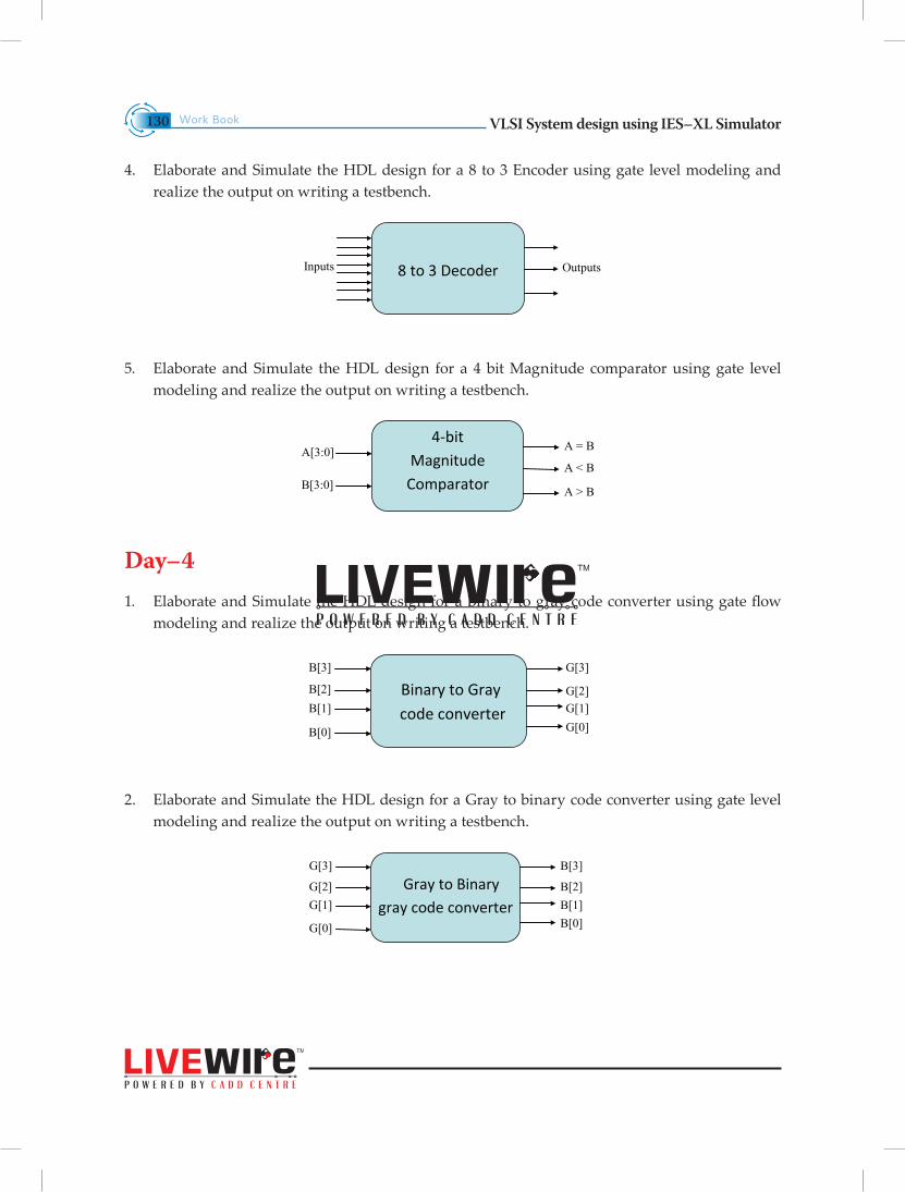
VLSI System design using IES–XL SimulatorWork Book130
4. Elaborate and Simulate the HDL design for a 8 to 3 Encoder using gate level modeling and realize the output on writing a testbench.
5. Elaborate and Simulate the HDL design for a 4 bit Magnitude comparator using gate level modeling and realize the output on writing a testbench.
Day–4 1. Elaborate and Simulate the HDL design for a Binary to gray code converter using gate flow
modeling and realize the output on writing a testbench.
2. Elaborate and Simulate the HDL design for a Gray to binary code converter using gate level modeling and realize the output on writing a testbench.
8 to 3 Decoder
Inputs Outputs
4-bit Magnitude
Comparator
A[3:0] A = B
A < B
B[3:0]
A > B
Binary to Gray code converter
B[3]
G[3]
B[2]
G[2]
B[1] G[1]
B[0] G[0]
Gray to Binary gray code converter
G[3]
B[3]
G[2]
B[2]
G[1] B[1]
G[0] B[0]
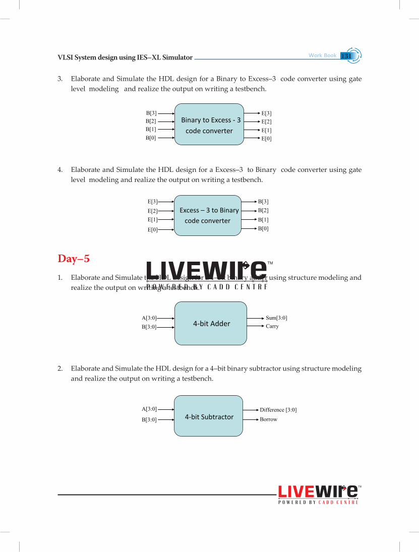
VLSI System design using IES–XL Simulator Work Book 131
3. Elaborate and Simulate the HDL design for a Binary to Excess–3 code converter using gate level modeling and realize the output on writing a testbench.
4. Elaborate and Simulate the HDL design for a Excess–3 to Binary code converter using gate level modeling and realize the output on writing a testbench.
Day–5 1. Elaborate and Simulate the HDL design for a 4–bit binary adder using structure modeling and
realize the output on writing a testbench.
2. Elaborate and Simulate the HDL design for a 4–bit binary subtractor using structure modeling and realize the output on writing a testbench.
Binary to Excess - 3 code converter
B[3] E[3] B[2] E[2] B[1] E[1]
B[0] E[0]
Excess – 3 to Binary code converter
E[3]
B[3]
E[2] B[2]
E[1] B[1]
E[0] B[0]
4-bit Adder
A[3:0]
Sum[3:0]
B[3:0] Carry
4-bit Subtractor
A[3:0] Difference [3:0]
B[3:0] Borrow
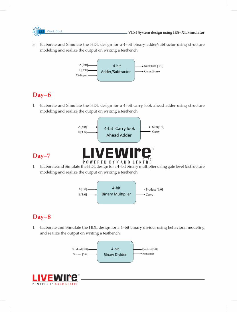
VLSI System design using IES–XL SimulatorWork Book132
3. Elaborate and Simulate the HDL design for a 4–bit binary adder/subtractor using structure modeling and realize the output on writing a testbench.
Day–6 1. Elaborate and Simulate the HDL design for a 4–bit carry look ahead adder using structure
modeling and realize the output on writing a testbench.
Day–7 1. Elaborate and Simulate the HDL design for a 4–bit binary multiplier using gate level & structure
modeling and realize the output on writing a testbench.
Day–8 1. Elaborate and Simulate the HDL design for a 4–bit binary divider using behavioral modeling
and realize the output on writing a testbench.
4-bit Adder/Subtractor
A[3:0] Sum/Diff [3:0]
B[3:0] Carry/Borro
Ctrlinput
4-bit Carry look Ahead Adder
A[3:0]
Sum[3:0]
B[3:0] Carry
4-bit Binary Multiplier
A[3:0] Product [6:0]
B[3:0] Carry
4-bit Binary Divider
Dividend [3:0]
Quotient [3:0] Divisor [3:0] Remainder
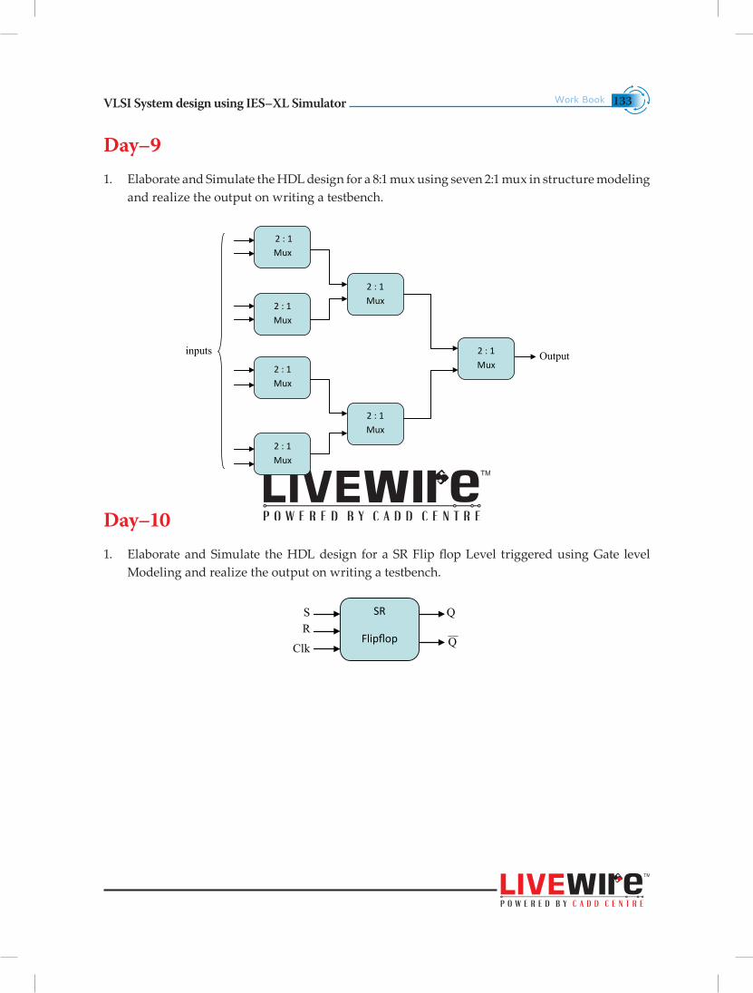
VLSI System design using IES–XL Simulator Work Book 133
Day–9 1. Elaborate and Simulate the HDL design for a 8:1 mux using seven 2:1 mux in structure modeling
and realize the output on writing a testbench.
Day–101. Elaborate and Simulate the HDL design for a SR Flip flop Level triggered using Gate level
Modeling and realize the output on writing a testbench.
2 : 1 Mux
2 : 1 Mux
2 : 1 Mux
2 : 1 Mux
2 : 1 Mux
2 : 1 Mux
2 : 1 Mux
inputs
Output
SR
Flipflop
S
Q
R Q
Clk
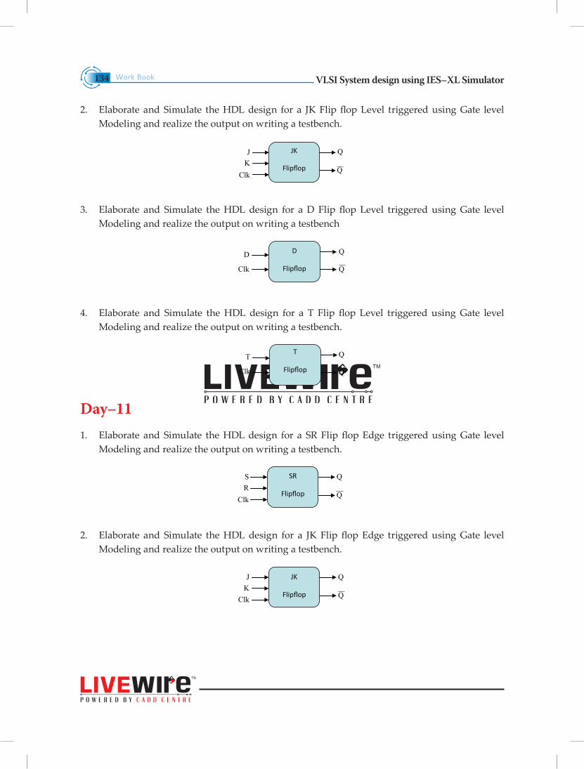
VLSI System design using IES–XL SimulatorWork Book134
2. Elaborate and Simulate the HDL design for a JK Flip flop Level triggered using Gate level Modeling and realize the output on writing a testbench.
3. Elaborate and Simulate the HDL design for a D Flip flop Level triggered using Gate level Modeling and realize the output on writing a testbench
4. Elaborate and Simulate the HDL design for a T Flip flop Level triggered using Gate level Modeling and realize the output on writing a testbench.
Day–111. Elaborate and Simulate the HDL design for a SR Flip flop Edge triggered using Gate level
Modeling and realize the output on writing a testbench.
2. Elaborate and Simulate the HDL design for a JK Flip flop Edge triggered using Gate level Modeling and realize the output on writing a testbench.
JK
Flipflop
J
Q
K Q
Clk
D
Flipflop
D
Q
Clk
Q
T
Flipflop
T
Q
Clk
Q
SR
Flipflop
S
Q
R Q
Clk
JK
Flipflop
J
Q
K Q
Clk
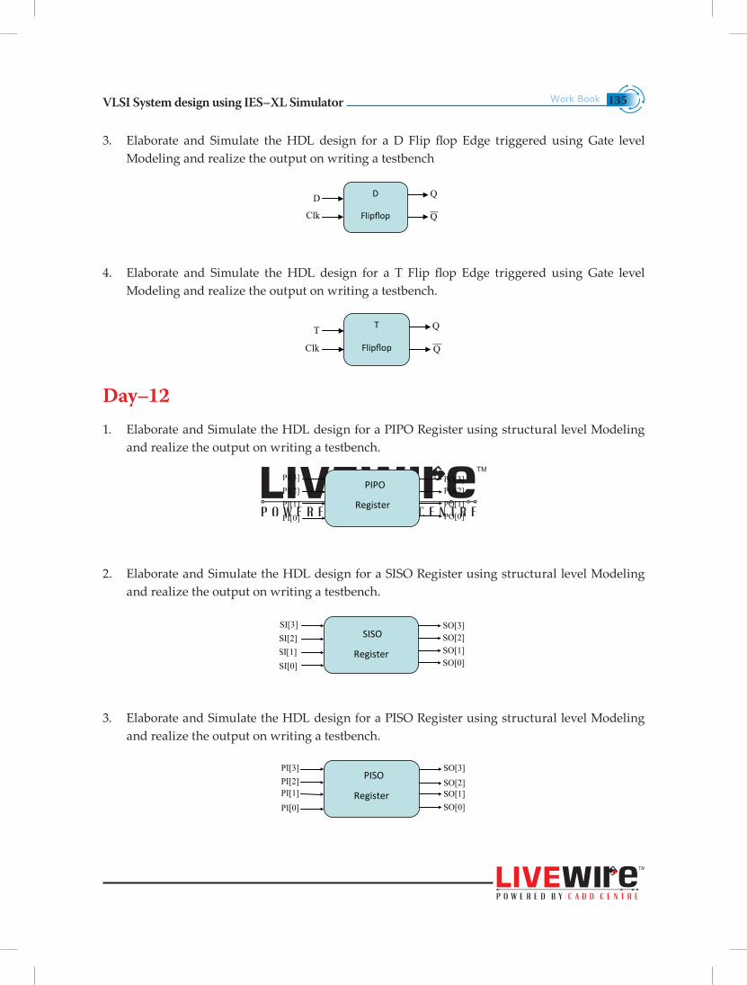
VLSI System design using IES–XL Simulator Work Book 135
3. Elaborate and Simulate the HDL design for a D Flip flop Edge triggered using Gate level Modeling and realize the output on writing a testbench
4. Elaborate and Simulate the HDL design for a T Flip flop Edge triggered using Gate level Modeling and realize the output on writing a testbench.
Day–121. Elaborate and Simulate the HDL design for a PIPO Register using structural level Modeling
and realize the output on writing a testbench.
2. Elaborate and Simulate the HDL design for a SISO Register using structural level Modeling and realize the output on writing a testbench.
3. Elaborate and Simulate the HDL design for a PISO Register using structural level Modeling and realize the output on writing a testbench.
D
Flipflop
D
Q
Clk
Q
T
Flipflop
T
Q
Clk
Q
PIPO
Register
PI[3] PO[3]
PI[2] PO[2]
PI[1] PO[1]PO[0]
PI[0]
SISO
Register
SI[3] SO[3]
SI[2] SO[2] SI[1]
SO[1]
SI[0] SO[0]
PISO
Register
PI[3] SO[3]
PI[2] SO[2]
PI[1] SO[1]
PI[0] SO[0]
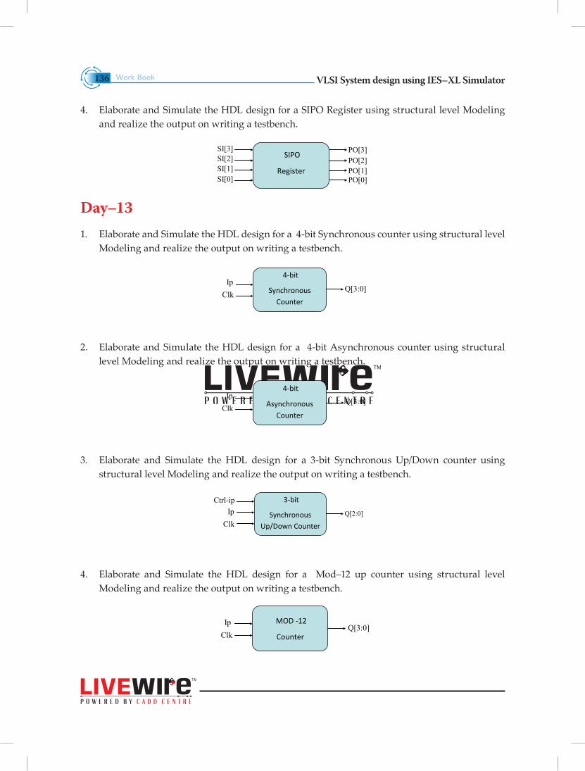
VLSI System design using IES–XL SimulatorWork Book136
4. Elaborate and Simulate the HDL design for a SIPO Register using structural level Modeling and realize the output on writing a testbench.
Day–131. Elaborate and Simulate the HDL design for a 4-bit Synchronous counter using structural level
Modeling and realize the output on writing a testbench.
2. Elaborate and Simulate the HDL design for a 4-bit Asynchronous counter using structural level Modeling and realize the output on writing a testbench.
3. Elaborate and Simulate the HDL design for a 3-bit Synchronous Up/Down counter using structural level Modeling and realize the output on writing a testbench.
4. Elaborate and Simulate the HDL design for a Mod–12 up counter using structural level Modeling and realize the output on writing a testbench.
SIPO
Register
SI[3]SI[2]SI[1]SI[0]
PO[3]PO[2]PO[1]PO[0]
4-bit
Synchronous Counter
Ip
Clk Q[3:0]
4-bit
Asynchronous Counter
Ip
Clk Q[3:0]
3-bit
Synchronous Up/Down Counter
Ctrl-ip
Ip
Clk Q[2:0]
MOD -12
Counter
Ip
Clk Q[3:0]
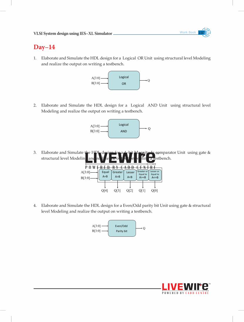
VLSI System design using IES–XL Simulator Work Book 137
Day–141. Elaborate and Simulate the HDL design for a Logical OR Unit using structural level Modeling
and realize the output on writing a testbench.
2. Elaborate and Simulate the HDL design for a Logical AND Unit using structural level Modeling and realize the output on writing a testbench.
3. Elaborate and Simulate the HDL design for a 4–bit Magnitude comparator Unit using gate & structural level Modeling and realize the output on writing a testbench.
4. Elaborate and Simulate the HDL design for a Even/Odd parity bit Unit using gate & structural level Modeling and realize the output on writing a testbench.
Logical
OR
A[3:0]
B[3:0] Q
Logical
AND
A[3:0]
B[3:0] Q
A[3:0]
B[3:0]
Q[4] Q[3] Q[2] Q[1] Q[0]
Greater A>B
Lesser
A<B
A>=B
Equal A=B
A<=B Greater or
Equal toLesser or Equal to
Even/Odd
Parity bit
A[3:0]
B[3:0] Q
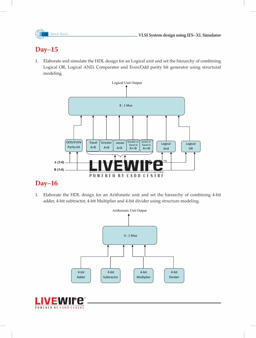
VLSI System design using IES–XL SimulatorWork Book138
Day–151. Elaborate and simulate the HDL design for an Logical unit and set the hierarchy of combining
Logical OR, Logical AND, Comparator and Even/Odd parity bit generator using structural modeling.
Day–16 1. Elaborate the HDL design for an Arithmetic unit and set the hierarchy of combining 4-bit
adder, 4-bit subtractor, 4-bit Multiplier and 4-bit divider using structure modeling.
Greater A>B
ODD/EVEN Parity bit
Logical And
Logical OR
8 : 1 Mux
Lesser
A<B
A>=B
Equal A=B
A<=B
Logical Unit Output
A [3:0]
B [3:0]
Greater or Equal to
Lesser or Equal to
4-bit Subtractor
4-bit Adder
4-bit Multiplier
4-bit Divider
4 : 1 Mux
Arithematic Unit Output
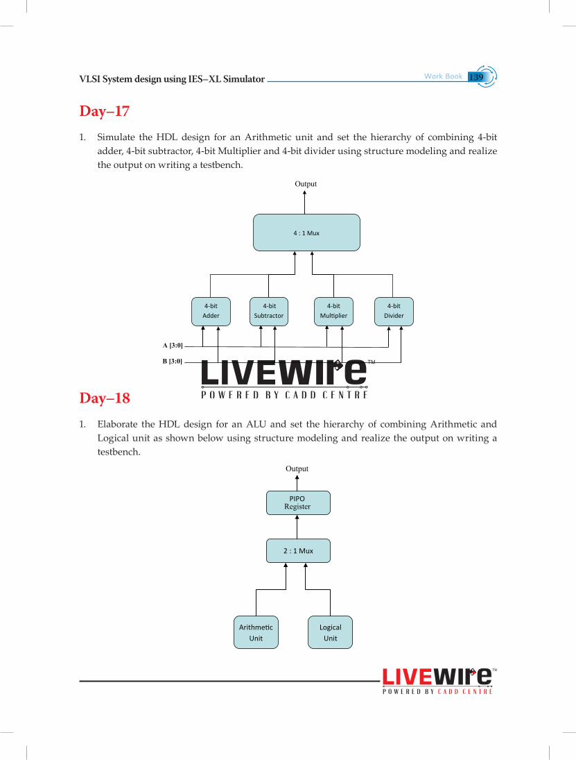
VLSI System design using IES–XL Simulator Work Book 139
Day–171. Simulate the HDL design for an Arithmetic unit and set the hierarchy of combining 4-bit
adder, 4-bit subtractor, 4-bit Multiplier and 4-bit divider using structure modeling and realize the output on writing a testbench.
Day–181. Elaborate the HDL design for an ALU and set the hierarchy of combining Arithmetic and
Logical unit as shown below using structure modeling and realize the output on writing a testbench.
4-bit Subtractor
4-bit Adder
4-bit Multiplier
4-bit Divider
4 : 1 Mux
Output
A [3:0]
B [3:0]
Arithmetic Unit
Logical Unit
2 : 1 Mux
PIPO
Output
Register
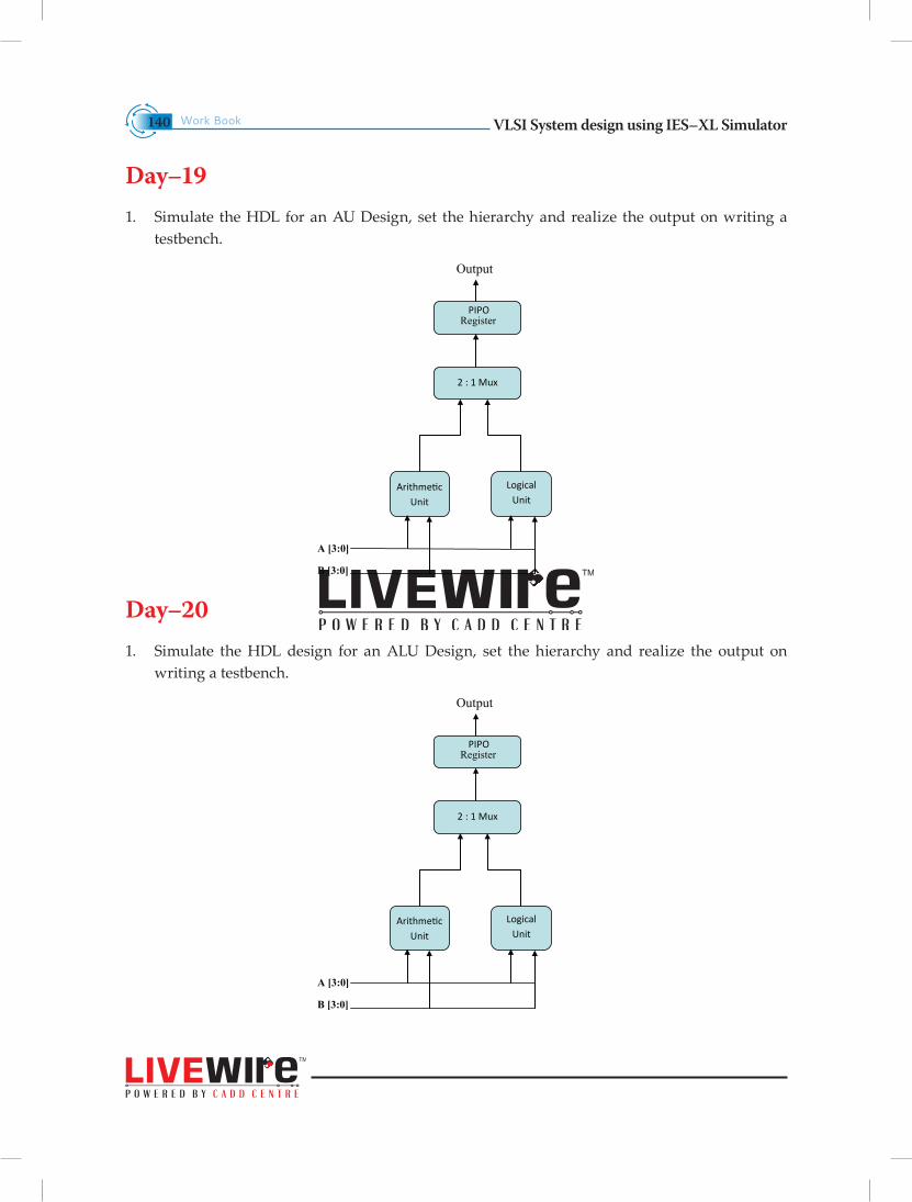
VLSI System design using IES–XL SimulatorWork Book140
Day–191. Simulate the HDL for an AU Design, set the hierarchy and realize the output on writing a
testbench.
Day–201. Simulate the HDL design for an ALU Design, set the hierarchy and realize the output on
writing a testbench.
Arithmetic Unit
Logical Unit
2 : 1 Mux
PIPO
Output
Register
A [3:0]
B [3:0]
Arithmetic Unit
Logical Unit
2 : 1 Mux
PIPO
Output
Register
A [3:0]
B [3:0]
I N D E X 141
IndexA
Alternate way of Simulation–1 36Alternate way of Simulation–2 42Always Statement 84Applying stimulus 27Arithmetic Operators 61Array of instances 18Assign & Deassign 103
B
Bitwise Operators 66Blocking & Nonblocking 86
C
Case Variation–casex, casez 98Combinational UDP 51Compilation of a Full adder 42Compiler Directives 114Concatenation Operators 70Conditional Operator 72Conditional Statement–case 97Conditional Statements 96Console–Simvision window 38Continuous Assignment 58
D
Data type declaration 26Day–1(workbook) 127Day–2 (workbook) 128Day–3 (workbook) 129Day–4 (workbook) 130Day–5 (workbook) 131Day–6 (workbook) 132Day–7 (workbook) 132Day–8 (workbook) 132Day–9 (workbook) 133Day–10 (workbook) 133Day–11 (workbook) 134Day–12 (workbook) 135Day–13 (workbook) 136
Day–14 (workbook) 137Day–15 (workbook) 138Day–16 (workbook) 138Day–17 (workbook) 139Day–18 (workbook) 139Day–19 (workbook) 140Day–20 (workbook) 140Delay Based timing control 89Delays 60Design browser–Simvision window 39Design of 4:1 Multiplexer 46, 76Display results 27
E
Elaboration of Full adder 44Equality Operators 65Event–Based Timing Control 93Event OR Timing control 94Examples for Gate Delays 21
F
Fall Delay 19Features of Testbench 26Features of Verilog 6Force 105Forever Loop 102For Loop 100Function 110
I
Implicit Continuous Assignment 59Implicit Continuous Assignment Delay 60Initial Statement 82Intra–Assignment Delay Control 91Invoking the Elaborator 34Invoking the simulator 35Invoking the Verilog Compiler 24
I N D E X142
L
Level Sensitive Control 95Logical Operators 62Loop Statements 99
M
Max Value 20Min Value 20Module 7Module instantiation 26
N
Name event control 94Net Declaration Delay 61Nets 9
O
Octal–to–Binary Encoder 74Operator Precedence 73
P
Parallel blocks 107Port Connection Rules 8Ports 7Procedural Assignments 85
R
Race around condition 88Reduction Operators 68Regular Assignment Delay 60Regular Delay Control 90Regular Event Control 94Relational Operators 64Release 105Repeat Loop 101Replication Operator 71Rise Delay 19
S
Schematic Tracer window 48Sequential blocks 106Sequential UDP’s 52Shift Operators 69Signal Contention 10Simulation of a Full adder 45Structured Procedures 82System Tasks 113
T
Tasks 108Test bench 25Timescale 116Timing Controls 89Turn–off Delay 20Types of Nets 9Typ Value 20
U
UDP format 50UDP Port Rules 49UDP Symbols 50User Defined Primitives 49
V
VLSI Design Methodology 4
W
While loop 99
Z
Zero Delay Control 93