Embed Size (px)
Citation preview
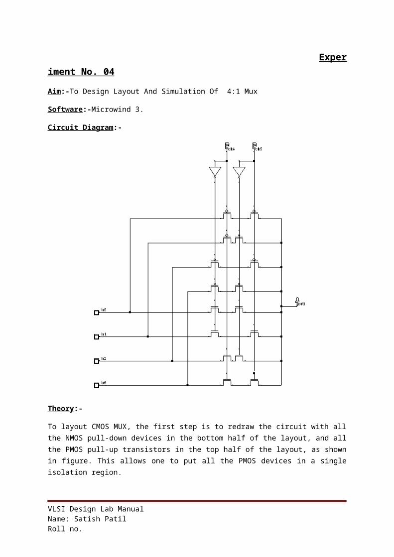
Experiment No. 04
Aim:-To Design Layout And Simulation Of 4:1 Mux
Software:-Microwind 3.
Circuit Diagram:-
Theory:-
To layout CMOS MUX, the first step is to redraw the circuit with all the NMOS pull-down devices in the bottom half of the layout, and all the PMOS pull-up transistors in the top half of the layout, as shown in figure. This allows one to put all the PMOS devices in a single isolation region.
While simple to lay out, conventional CMOS multiplexers take lots of real estate. The pull-down part of the circuit is an NMOS multiplexer and pass transistor logic must supply both pull-up and pull-down paths.A static pull-up can be obtained by running the output, out through an inverter and feeding the inverted signal, out-BAR , to the gate of a PMOS pull-up transistor.
VLSI Design Lab ManualName: Satish Patil Roll no.

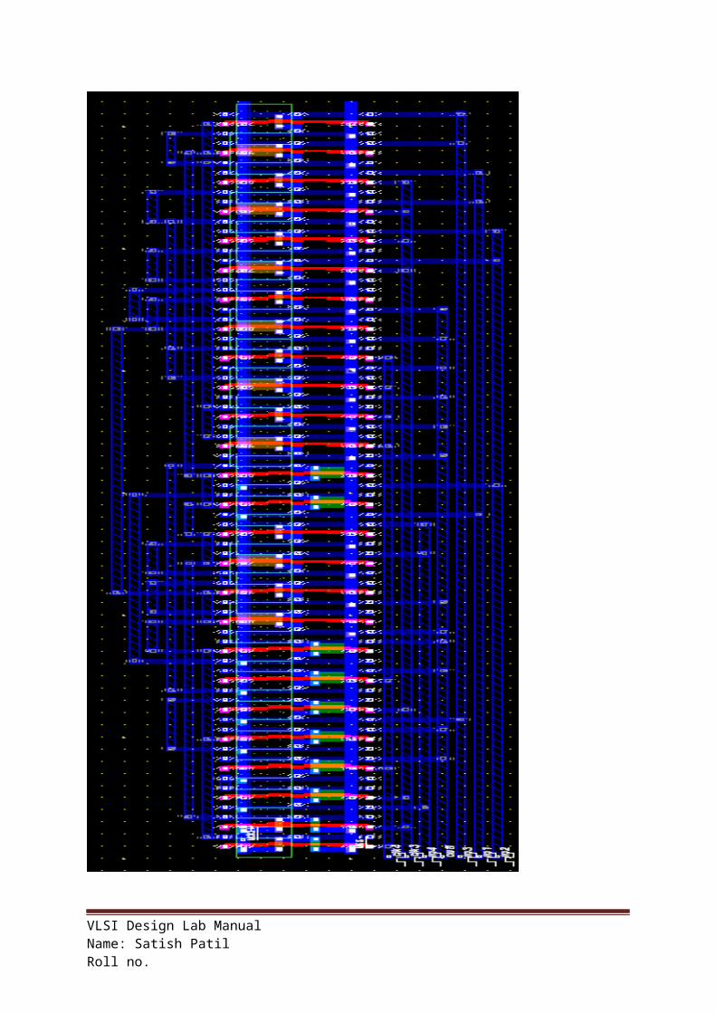
Layout:-
VLSI Design Lab ManualName: Satish Patil Roll no.
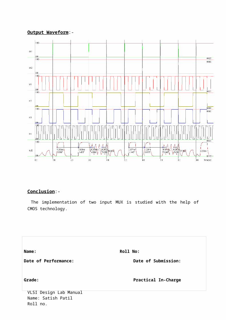
Output Waveform:-
Conclusion:-
The implementation of two input MUX is studied with the help of CMOS technology.
VLSI Design Lab ManualName: Satish Patil Roll no.
Name: Roll No:
Date of Performance: Date of Submission:
Grade: Practical In-Charge
VLSI Design Lab ManualName: Satish Patil Roll no.


![Etu02 Mux Man[1]](https://img.pdfslide.us/doc/110x75/5436e8ae219acd5b118b477c/etu02-mux-man1.jpg)