Embed Size (px)
Citation preview
VLSI Design
Circuits & Layout
Outline
CMOS Gate Design Pass Transistors CMOS Latches & Flip-Flops Standard Cell Layouts Stick Diagrams
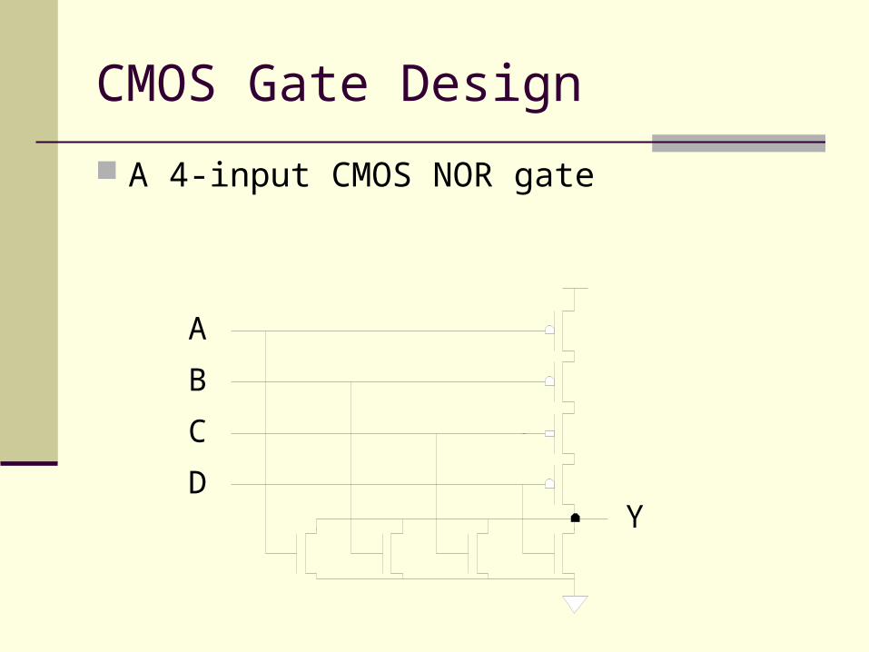
CMOS Gate Design
A 4-input CMOS NOR gate
A
B
C
DY
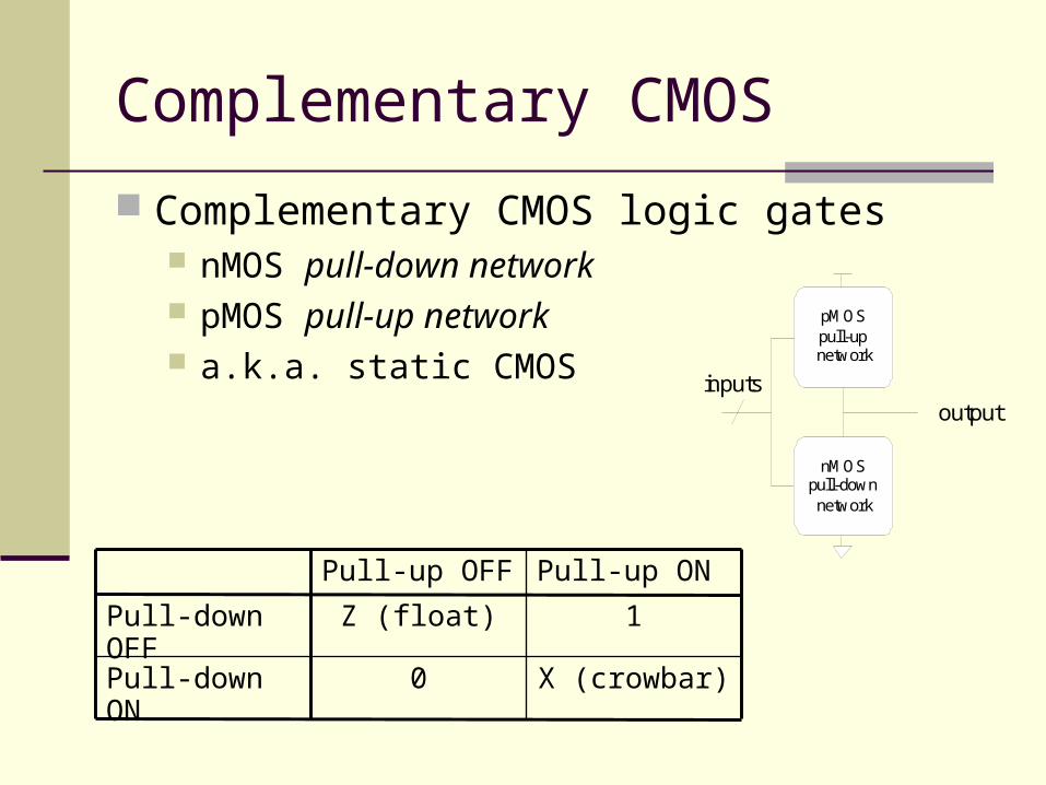
Complementary CMOS
Complementary CMOS logic gates nMOS pull-down network pMOS pull-up network a.k.a. static CMOS
pMOSpull-upnetwork
outputinputs
nMOSpull-downnetwork
X (crowbar)0Pull-down ON
1Z (float)Pull-down OFF
Pull-up ONPull-up OFF
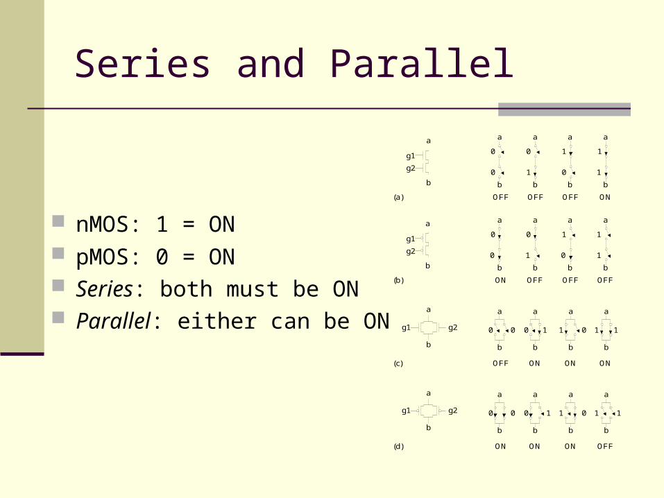
Series and Parallel
nMOS: 1 = ON pMOS: 0 = ON Series: both must be ON Parallel: either can be ON
(a)
a
b
a
b
g1
g2
0
0
a
b
0
1
a
b
1
0
a
b
1
1
OFF OFF OFF ON
(b)
a
b
a
b
g1
g2
0
0
a
b
0
1
a
b
1
0
a
b
1
1
ON OFF OFF OFF
(c)
a
b
a
b
g1 g2 0 0
OFF ON ON ON
(d) ON ON ON OFF
a
b
0
a
b
1
a
b
11 0 1
a
b
0 0
a
b
0
a
b
1
a
b
11 0 1
a
b
g1 g2
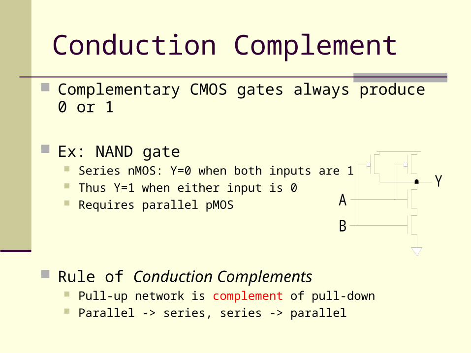
Conduction Complement Complementary CMOS gates always produce 0 or 1
Ex: NAND gate Series nMOS: Y=0 when both inputs are 1 Thus Y=1 when either input is 0 Requires parallel pMOS
Rule of Conduction Complements Pull-up network is complement of pull-down Parallel -> series, series -> parallel
A
B
Y
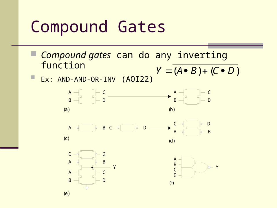
Compound Gates
Compound gates can do any inverting function Ex: AND-AND-OR-INV (AOI22)
A
B
C
D
A
B
C
D
A B C DA B
C D
B
D
YA
CA
C
A
B
C
D
B
D
Y
(a)
(c)
(e)
(b)
(d)
(f)
)()( DCBAY
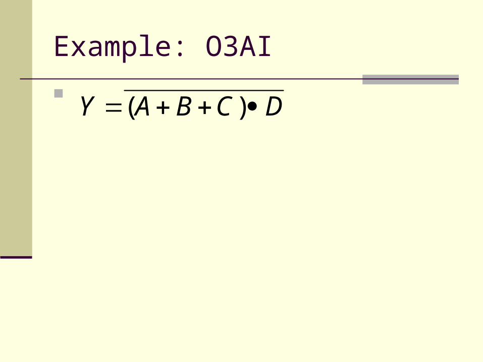
Example: O3AI
DCBAY )(
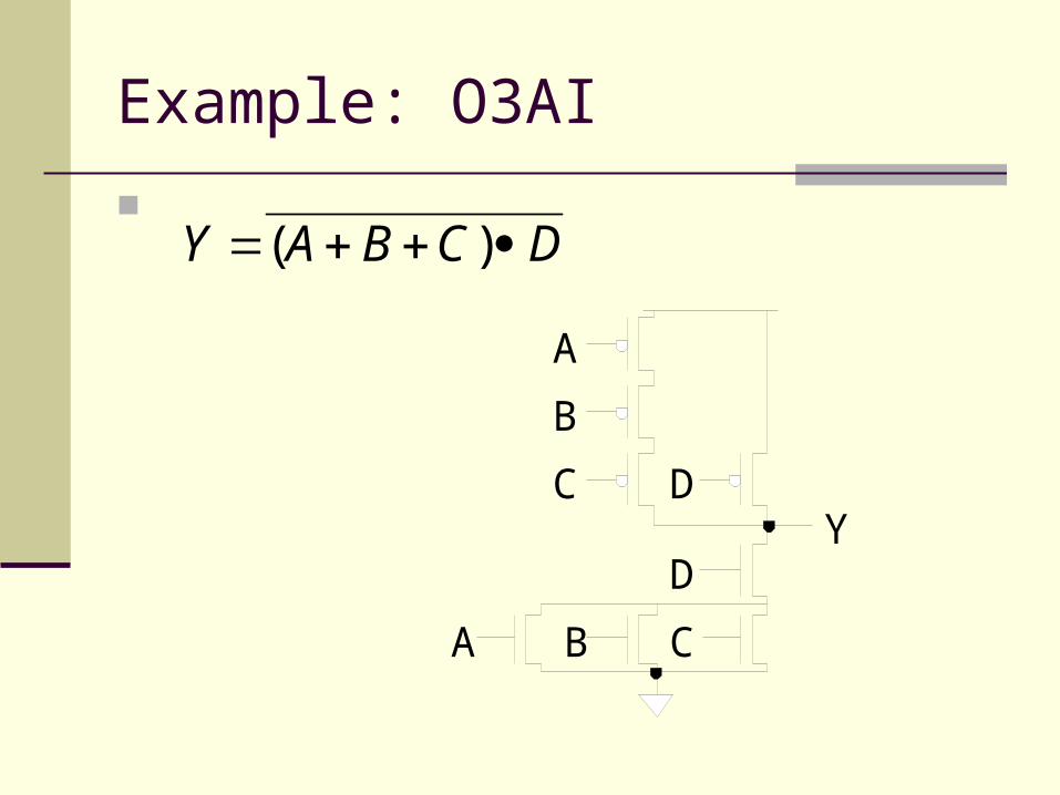
Example: O3AI
A B
Y
C
D
DC
B
A
DCBAY )(
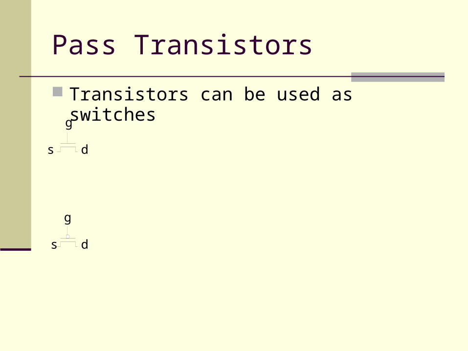
Pass Transistors
Transistors can be used as switches
g
s d
g
s d
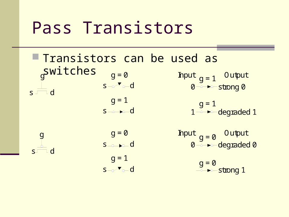
Pass Transistors
Transistors can be used as switches
g
s d
g = 0s d
g = 1s d
0 strong 0
Input Output
1 degraded 1
g
s d
g = 0
s d
g = 1
s d
0 degraded 0
Input Output
strong 1
g = 1
g = 1
g = 0
g = 0
Signal Strength
Strength of signal How close it approximates ideal voltage source
VDD and GND rails are strongest 1 and 0
nMOS pass strong 0 But degraded or weak 1
pMOS pass strong 1 But degraded or weak 0
Thus NMOS are best for pull-down network Thus PMOS are best for pull-up network
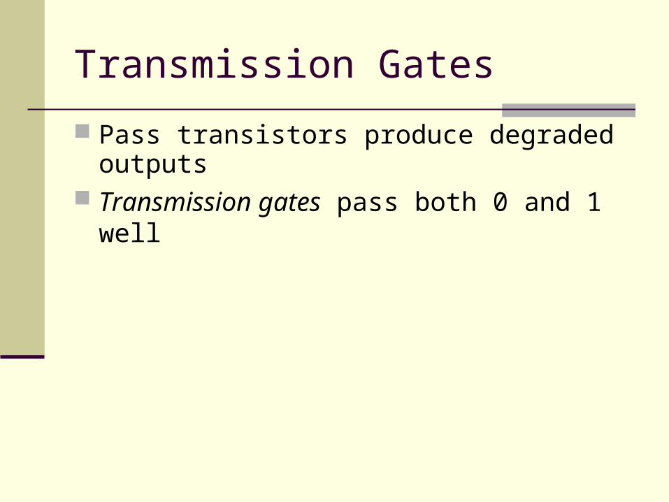
Transmission Gates
Pass transistors produce degraded outputs Transmission gates pass both 0 and 1 well
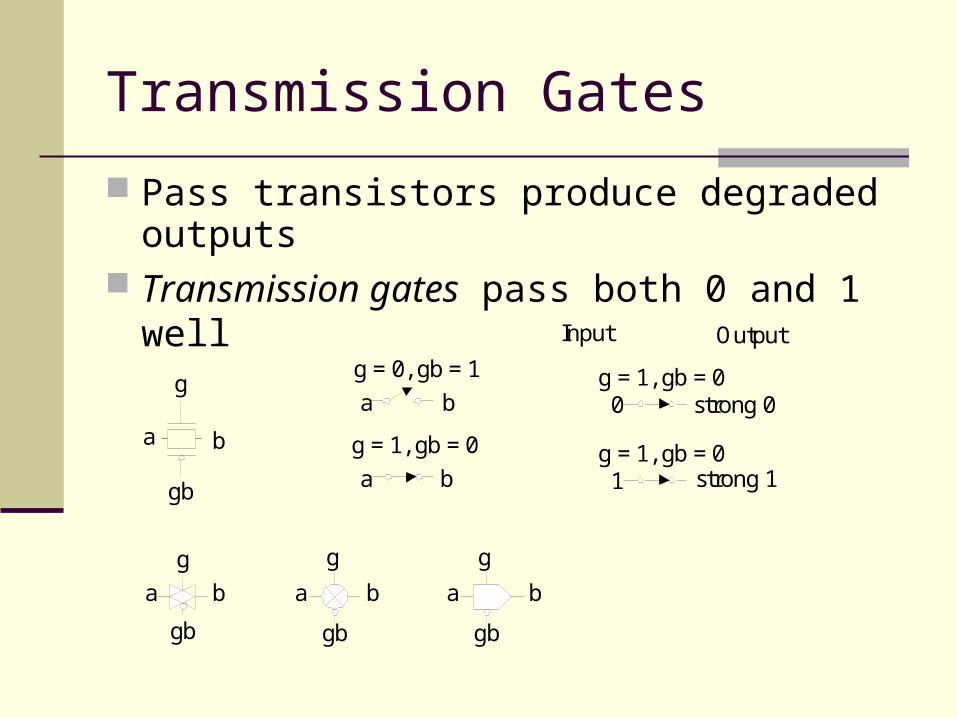
Transmission Gates
Pass transistors produce degraded outputs Transmission gates pass both 0 and 1 well
g = 0, gb = 1
a b
g = 1, gb = 0
a b
0 strong 0
Input Output
1 strong 1
g
gb
a b
a b
g
gb
a b
g
gb
a b
g
gb
g = 1, gb = 0
g = 1, gb = 0
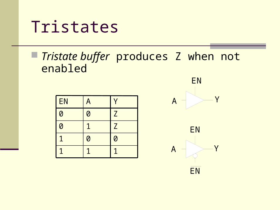
Tristates
Tristate buffer produces Z when not enabled
111
001
Z10
Z00
YAEN A Y
EN
A Y
EN
EN
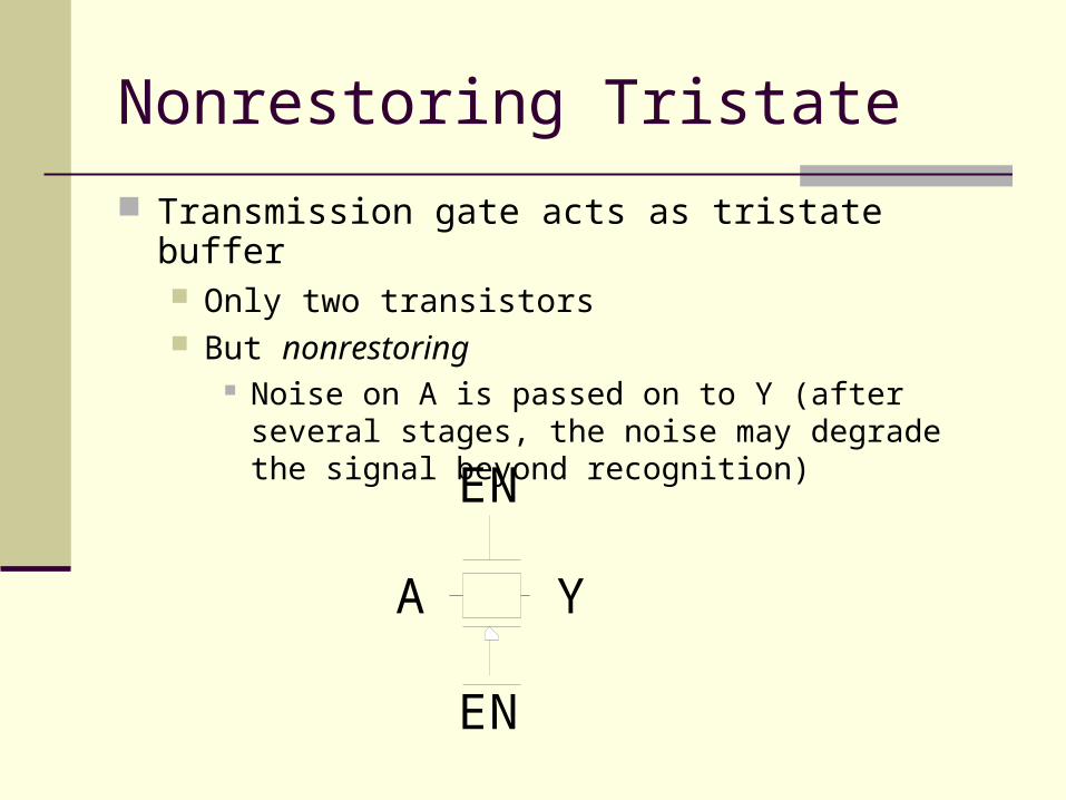
Nonrestoring Tristate
Transmission gate acts as tristate buffer Only two transistors But nonrestoring
Noise on A is passed on to Y (after several stages, the noise may degrade the signal beyond recognition)
A Y
EN
EN
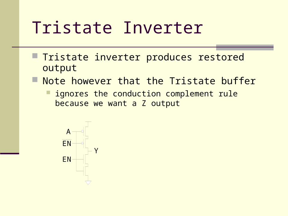
Tristate Inverter
Tristate inverter produces restored output Note however that the Tristate buffer
ignores the conduction complement rule because we want a Z output
A
YEN
EN
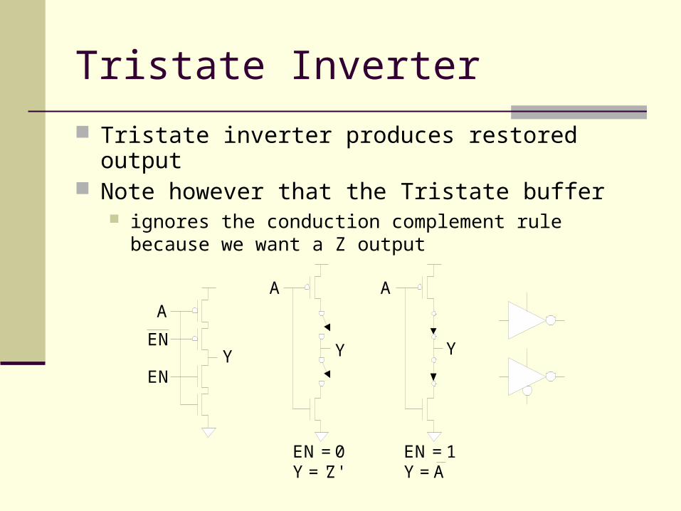
Tristate Inverter
Tristate inverter produces restored output Note however that the Tristate buffer
ignores the conduction complement rule because we want a Z output
A
YEN
A
Y
EN = 0Y = 'Z'
Y
EN = 1Y = A
A
EN
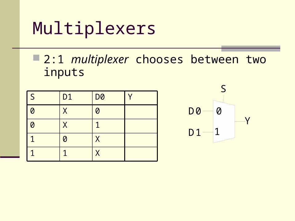
Multiplexers
2:1 multiplexer chooses between two inputs
X11
X01
1X0
0X0
YD0D1S
0
1
S
D0
D1Y
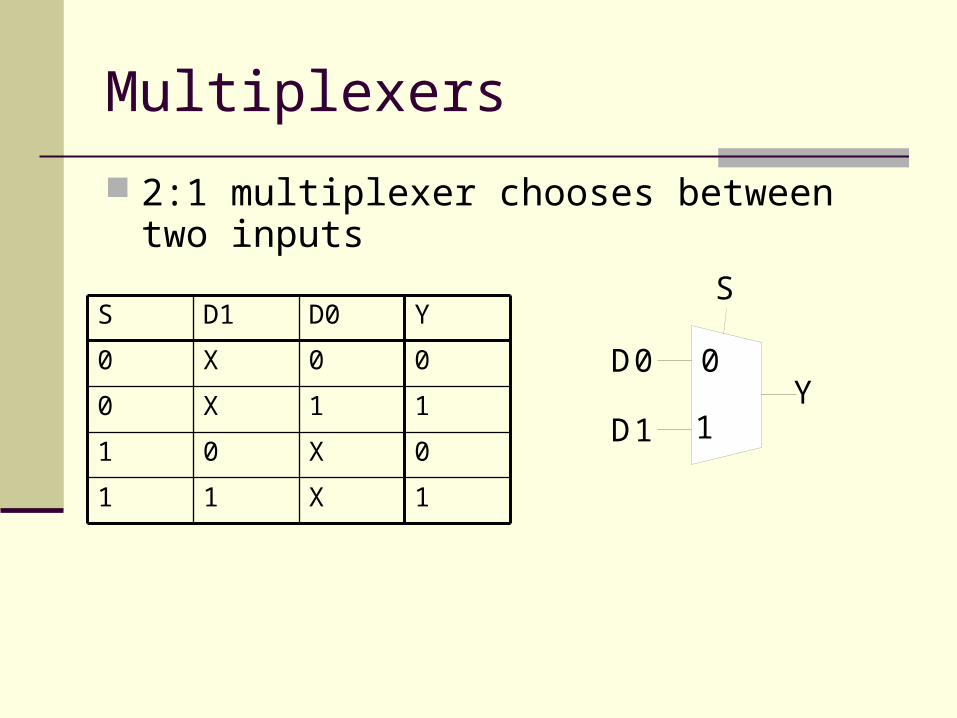
Multiplexers
2:1 multiplexer chooses between two inputs
1X11
0X01
11X0
00X0
YD0D1S
0
1
S
D0
D1Y
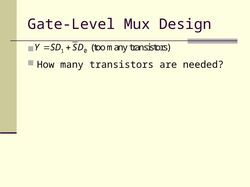
Gate-Level Mux Design
How many transistors are needed?
1 0 (too many transistors)Y SD SD
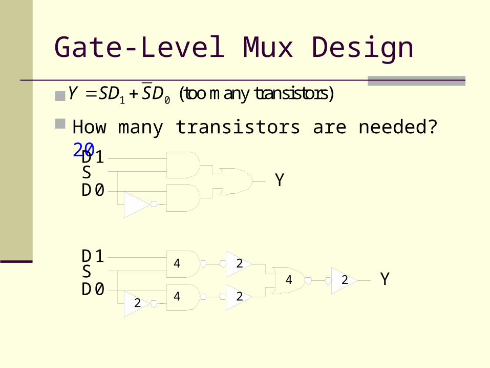
Gate-Level Mux Design
How many transistors are needed? 20
1 0 (too many transistors)Y SD SD
44
D1
D0S Y
4
2
22 Y
2
D1
D0S
Transmission Gate Mux
Nonrestoring mux uses two transmission gates
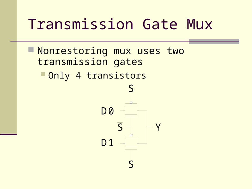
Transmission Gate Mux
Nonrestoring mux uses two transmission gates Only 4 transistors
S
S
D0
D1
YS
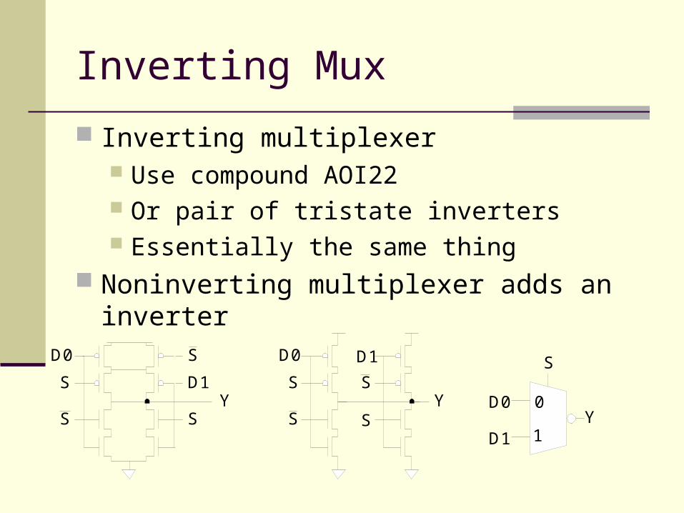
Inverting Mux
Inverting multiplexer Use compound AOI22 Or pair of tristate inverters Essentially the same thing
Noninverting multiplexer adds an inverter
S
D0 D1
Y
S
D0
D1Y
0
1S
Y
D0
D1
S
S
S
S
S
S
4:1 Multiplexer
4:1 mux chooses one of 4 inputs using two selects
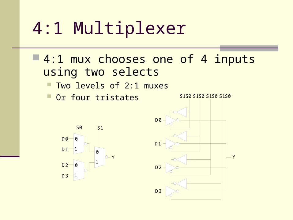
4:1 Multiplexer
4:1 mux chooses one of 4 inputs using two selects Two levels of 2:1 muxes Or four tristates
S0
D0
D1
0
1
0
1
0
1Y
S1
D2
D3
D0
D1
D2
D3
Y
S1S0 S1S0 S1S0 S1S0
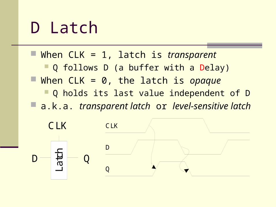
D Latch
When CLK = 1, latch is transparent Q follows D (a buffer with a Delay)
When CLK = 0, the latch is opaque Q holds its last value independent of D
a.k.a. transparent latch or level-sensitive latch
CLK
D Q
Latc
h D
CLK
Q
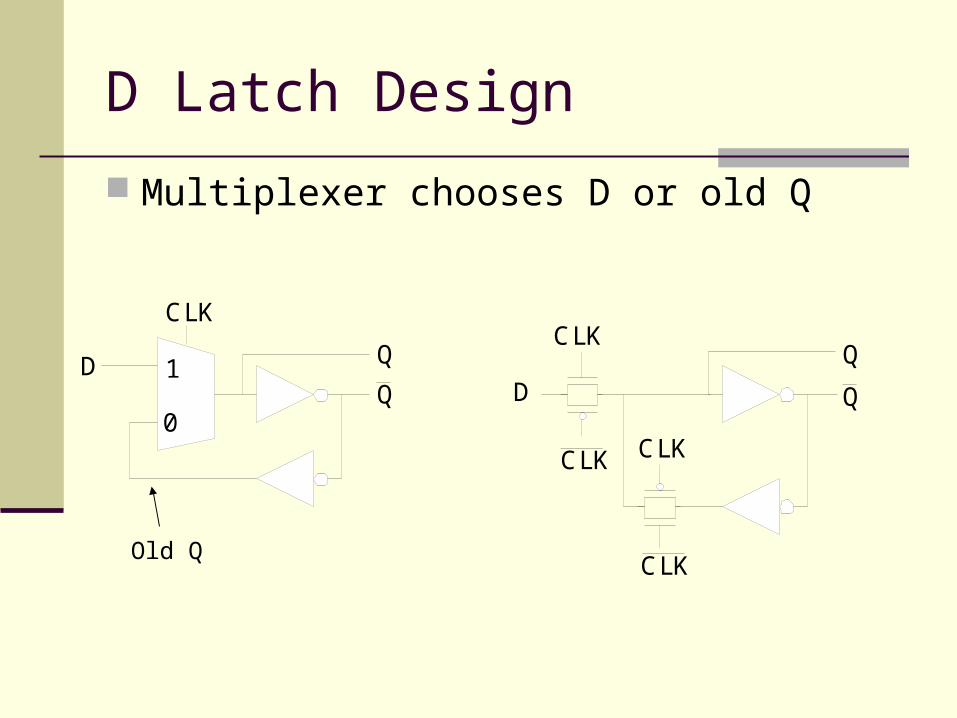
D Latch Design
Multiplexer chooses D or old Q
1
0
D
CLK
QCLK
CLKCLK
CLK
DQ Q
Q
Old Q
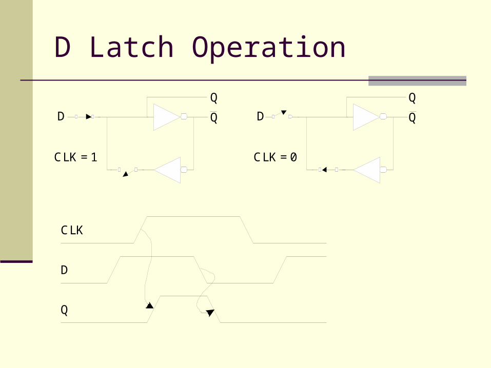
D Latch Operation
CLK = 1
D Q
Q
CLK = 0
D Q
Q
D
CLK
Q
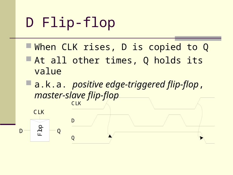
D Flip-flop
When CLK rises, D is copied to Q At all other times, Q holds its value a.k.a. positive edge-triggered flip-flop, master-
slave flip-flop
Flo
p
CLK
D Q
D
CLK
Q
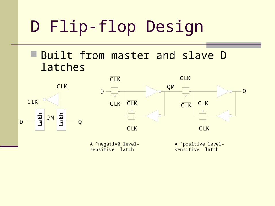
D Flip-flop Design
Built from master and slave D latches
QM
CLK
CLKCLK
CLK
Q
CLK
CLK
CLK
CLK
D
Latc
h
Latc
h
D QQM
CLK
CLK
A “negative level-sensitive” latch A “positive level-sensitive” latch
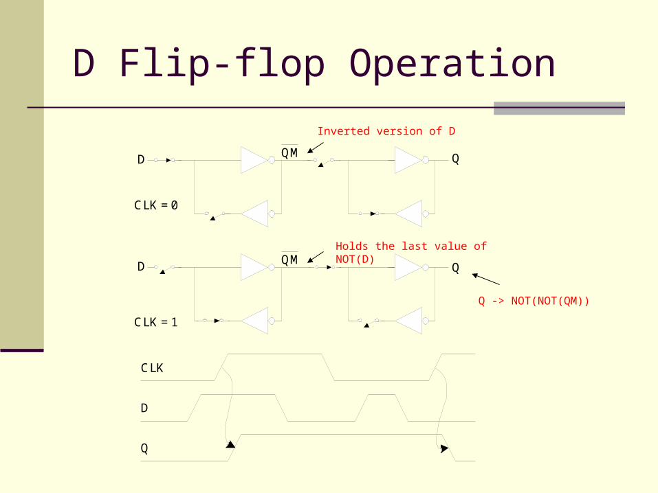
D Flip-flop Operation
CLK = 1
D
CLK = 0
Q
D
QM
QMQ
D
CLK
Q
Inverted version of D
Q -> NOT(NOT(QM))
Holds the last value of NOT(D)
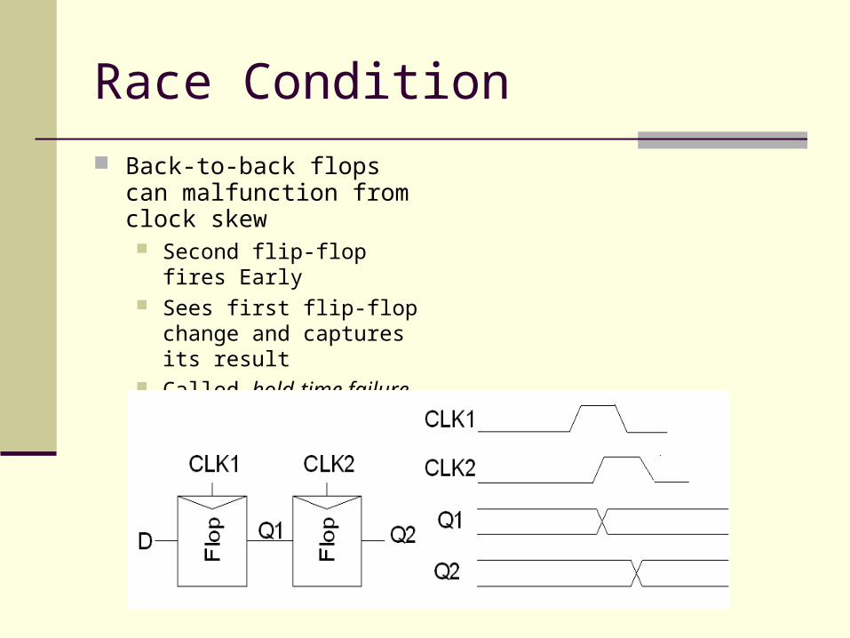
Race Condition
Back-to-back flops can malfunction from clock skew Second flip-flop fires Early Sees first flip-flop change
and captures its result Called hold-time failure or
race condition
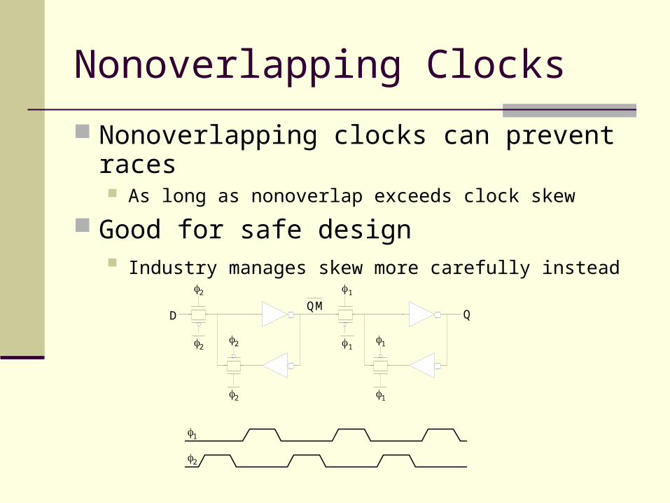
Nonoverlapping Clocks
Nonoverlapping clocks can prevent races As long as nonoverlap exceeds clock skew
Good for safe design Industry manages skew more carefully instead
1
11
1
2
22
2
2
1
QMQD
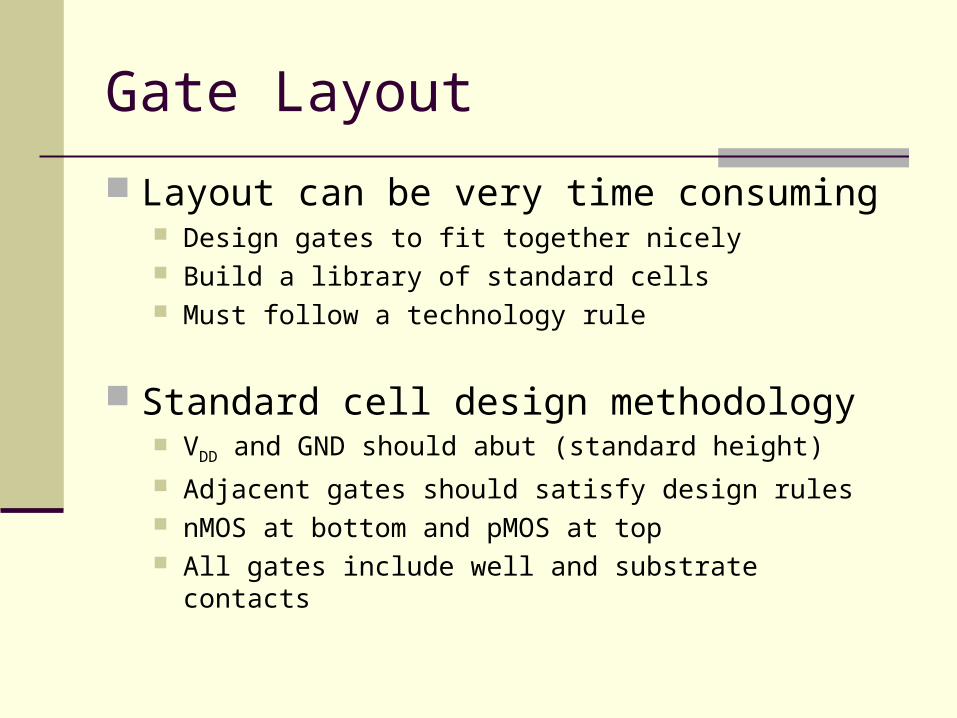
Gate Layout
Layout can be very time consuming Design gates to fit together nicely Build a library of standard cells Must follow a technology rule
Standard cell design methodology VDD and GND should abut (standard height)
Adjacent gates should satisfy design rules nMOS at bottom and pMOS at top All gates include well and substrate contacts
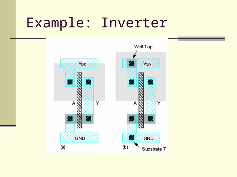
Example: Inverter
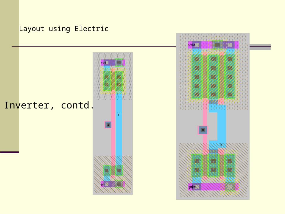
Inverter, contd..
Layout using Electric
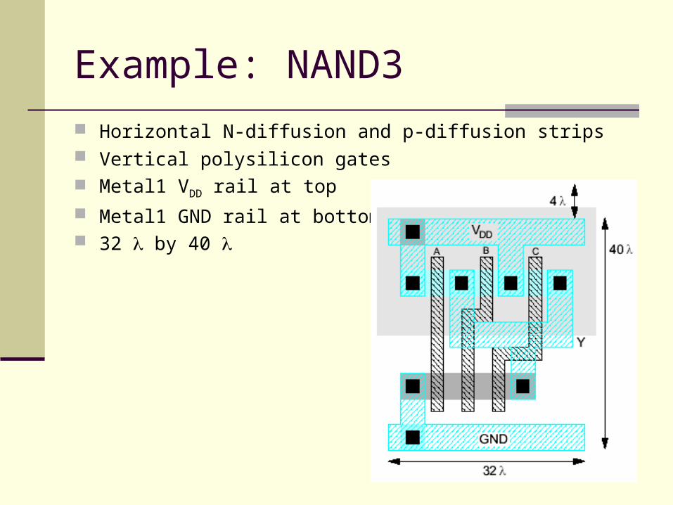
Example: NAND3
Horizontal N-diffusion and p-diffusion strips Vertical polysilicon gates Metal1 VDD rail at top
Metal1 GND rail at bottom 32 by 40
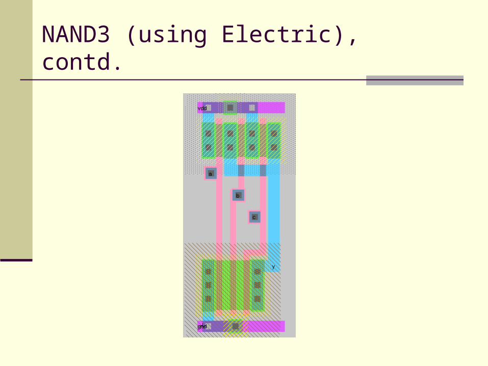
NAND3 (using Electric), contd.
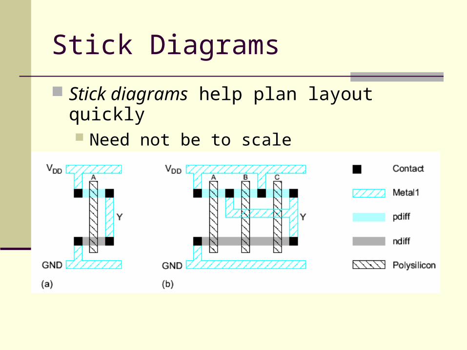
Stick Diagrams
Stick diagrams help plan layout quickly Need not be to scale Draw with color pencils or dry-erase markers
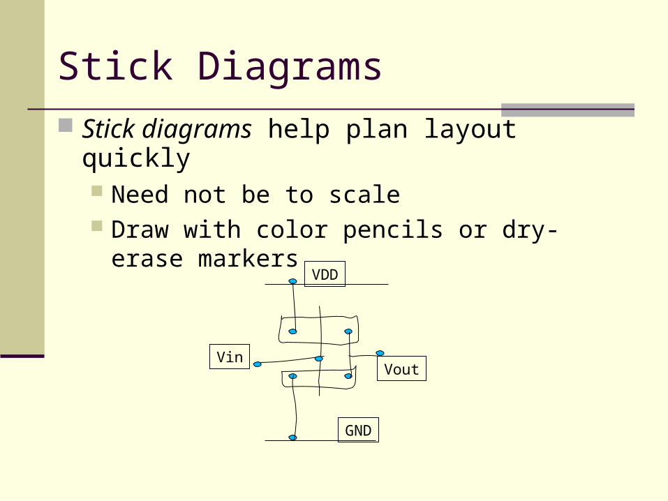
Stick Diagrams
Stick diagrams help plan layout quickly Need not be to scale Draw with color pencils or dry-erase markers
VinVout
VDD
GND
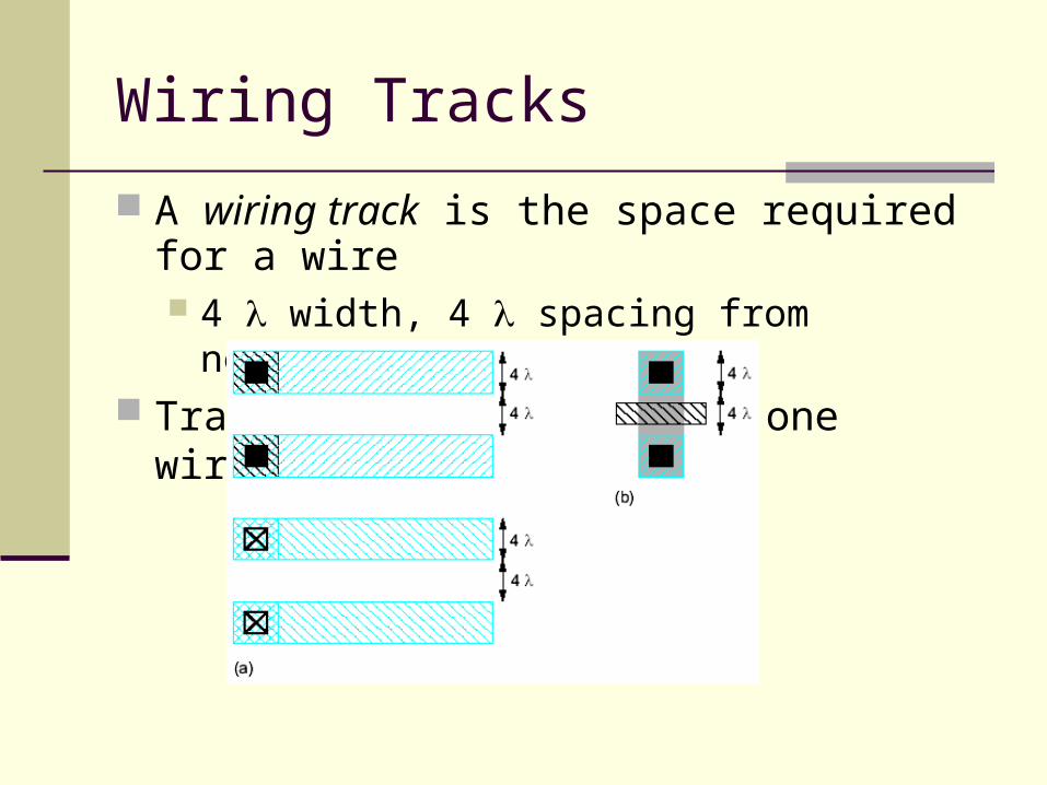
Wiring Tracks
A wiring track is the space required for a wire 4 width, 4 spacing from neighbor = 8
pitch Transistors also consume one wiring track
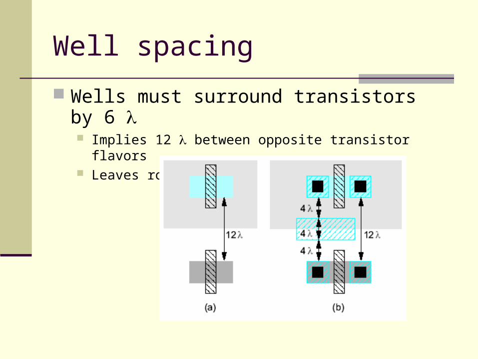
Well spacing
Wells must surround transistors by 6 Implies 12 between opposite transistor flavors Leaves room for one wire track
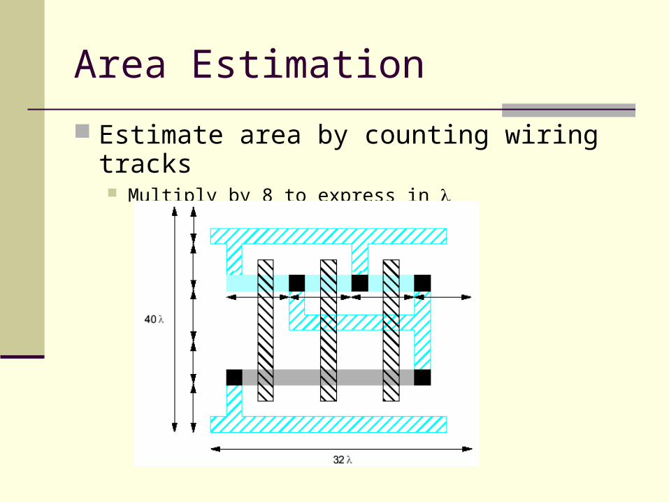
Area Estimation
Estimate area by counting wiring tracks Multiply by 8 to express in
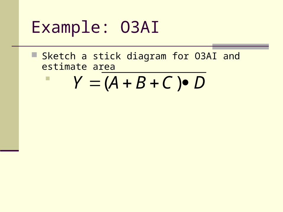
Example: O3AI
Sketch a stick diagram for O3AI and estimate area
DCBAY )(
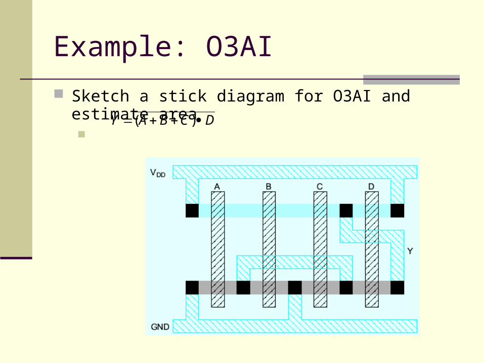
Example: O3AI
Sketch a stick diagram for O3AI and estimate area DCBAY )(
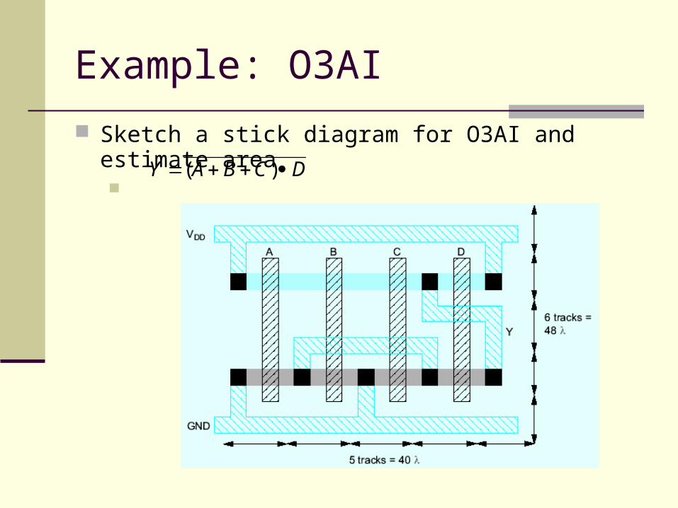
Example: O3AI
Sketch a stick diagram for O3AI and estimate area DCBAY )(