Embed Size (px)
DESCRIPTION
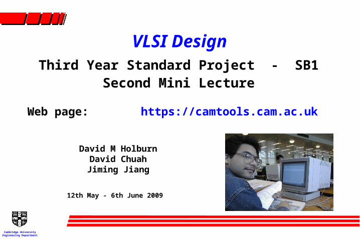
VLSI Design. Third Year Standard Project - SB1 Second Mini Lecture Web page: https://camtools.cam.ac.uk. David M Holburn David Chuah Jiming Jiang. 12th May - 6th June 2009. Summary of progress so far. Developed ring oscillator (RO) concept Confirmed using VHDL & ModelSim - PowerPoint PPT Presentation
Citation preview
Cambridge University
Engineering Department
VLSI DesignThird Year Standard Project - SB1
Second Mini Lecture
Web page: https://camtools.cam.ac.uk
12th May - 6th June 2009
David M HolburnDavid ChuahJiming Jiang
Cambridge University
Engineering Department
Summary of progress so far Developed ring oscillator (RO) concept Confirmed using VHDL & ModelSim Explored effect of varying NOR delays
(ModelSim) Built symbol & schematic Incorporated RO in Frequency Synthesiser
design Used Eldo to predict timing characteristics of
RO using AMS NOR2 design Investigated characteristics of real RO
design using oscilloscope/counter
Cambridge University
Engineering Department
Labs 5 & 6
Lab Guide 5 Gain familiarity with layout and IC Station layout editor Adapt mask layouts for the 2-input NOR gate nor2x Identify/correct design rule violations in nor2 layout
Lab Guide 6 Verification - check for proper correspondence between
your nor2x layout & the nor2x transistor schematic Check transistor dimensions W & L Investigate effect of parasitic elements C and R in layout Simulate the gate’s characteristics with parasitics using
Eldo
Cambridge University
Engineering Department
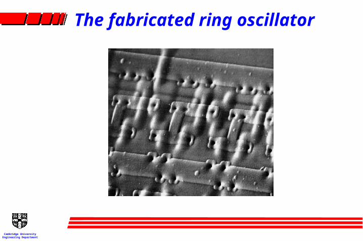
The fabricated ring oscillator
Cambridge University
Engineering Department
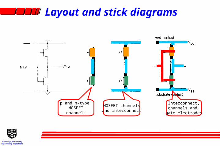
Layout and stick diagrams
p and n-type MOSFETchannels
MOSFET channelsand interconnect
Interconnect,channels and
gate electrodes
Cambridge University
Engineering Department
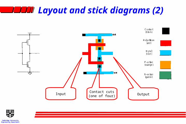
Layout and stick diagrams (2)
OutputContact cuts(one of four)
Input
Cambridge University
Engineering Department
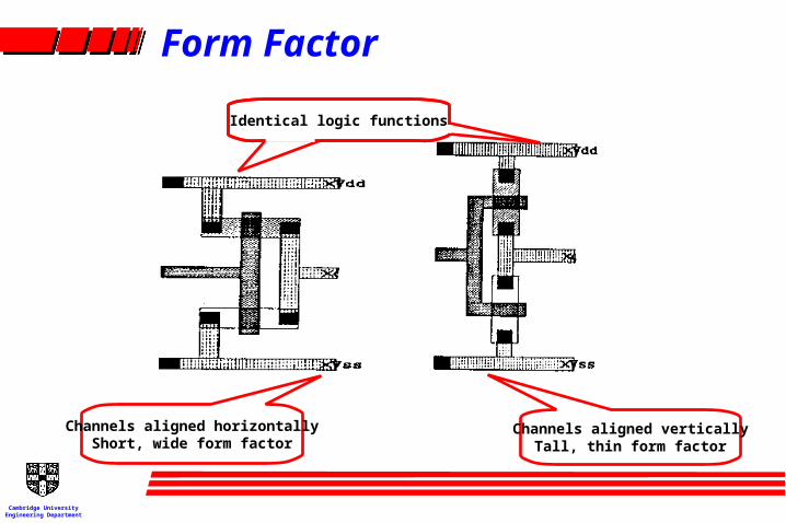
Form Factor
Channels aligned horizontallyShort, wide form factor
Channels aligned verticallyTall, thin form factor
Identical logic functions
Cambridge University
Engineering Department
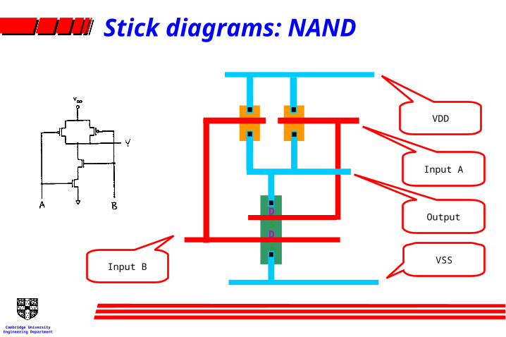
Stick diagrams: NAND
Output
Input B
Input A
VDD
VSS
D
SD
S
Cambridge University
Engineering Department
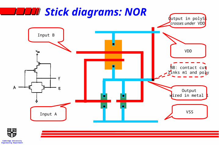
Output in polySicrosses under VDD
Stick diagrams: NOR
Outputwired in metal 1
Input B
Input A
VDD
VSS
NB: contact cutlinks m1 and poly
Cambridge University
Engineering Department
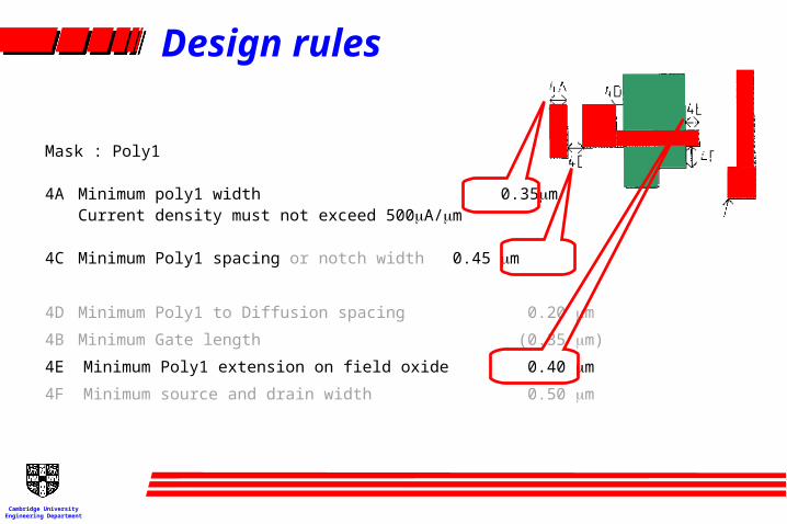
Design rules
Mask : Poly1
4A Minimum poly1 width 0.35m Current density must not exceed 500A/m
4C Minimum Poly1 spacing or notch width 0.45 m
4D Minimum Poly1 to Diffusion spacing 0.20 m
4B Minimum Gate length (0.35 m)
4E Minimum Poly1 extension on field oxide 0.40 m
4F Minimum source and drain width 0.50 m
Cambridge University
Engineering Department
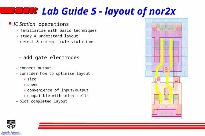
Lab Guide 5 - layout of nor2x
– add gate electrodes
IC Station operations– familiarise with basic techniques– study & understand layout– detect & correct rule violations
– connect output– consider how to optimise layout
» size» speed» convenience of input/output» compatible with other cells
– plot completed layout
Cambridge University
Engineering Department
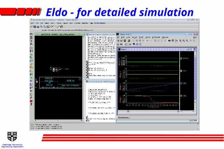
Eldo - for detailed simulation
Cambridge University
Engineering Department
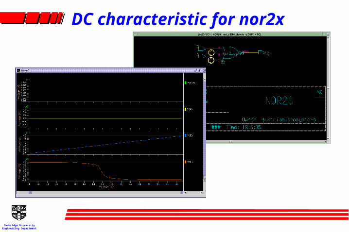
DC characteristic for nor2x
Cambridge University
Engineering Department
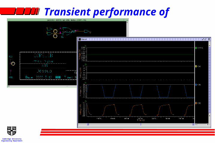
Transient performance of nor2x
Cambridge University
Engineering Department
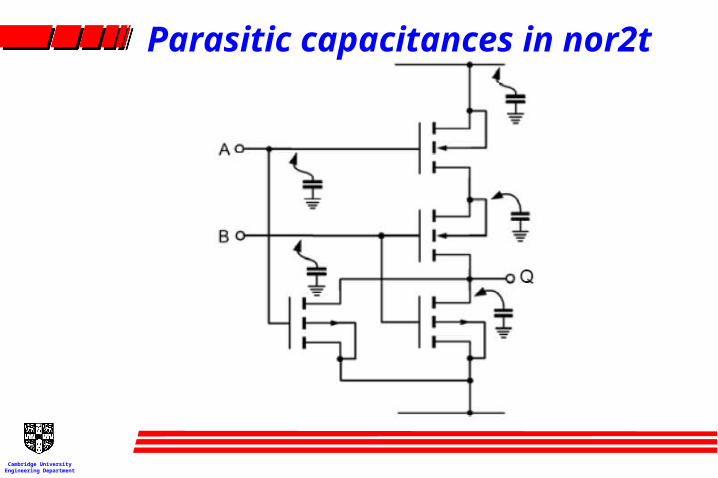
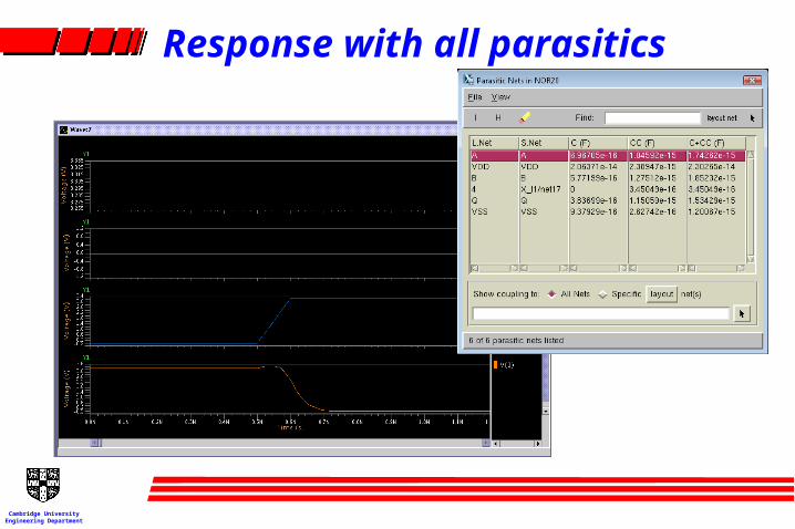
Parasitic capacitances in nor2t
Cambridge University
Engineering Department
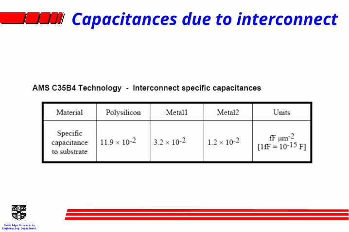
Capacitances due to interconnect
Cambridge University
Engineering Department
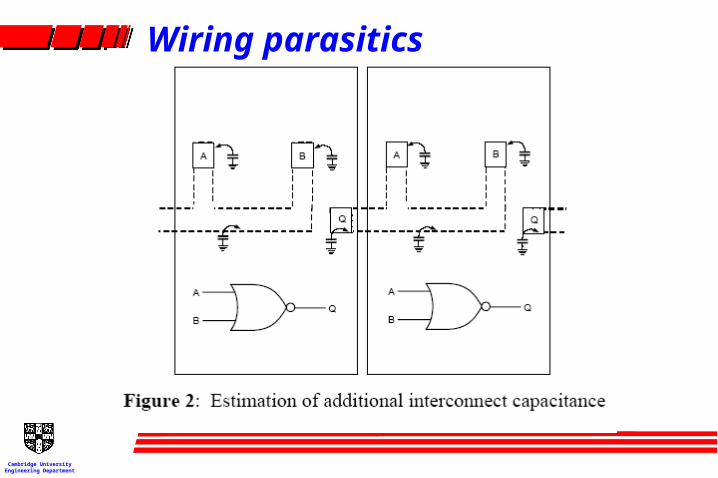
Wiring parasitics
Cambridge University
Engineering Department
Response with all parasitics
Cambridge University
Engineering Department
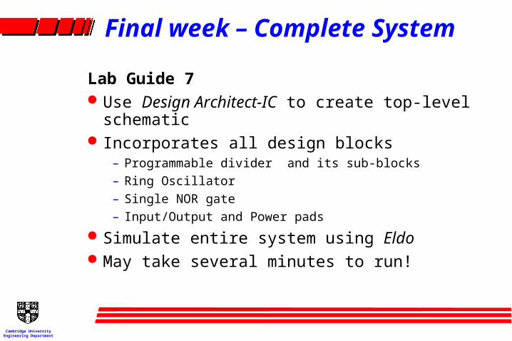
Final week – Complete System
Lab Guide 7 Use Design Architect-IC to create top-level
schematic Incorporates all design blocks
– Programmable divider and its sub-blocks– Ring Oscillator– Single NOR gate– Input/Output and Power pads
Simulate entire system using Eldo May take several minutes to run!
Cambridge University
Engineering Department
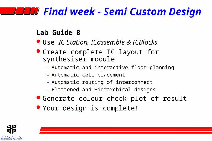
Final week - Semi Custom Design
Lab Guide 8 Use IC Station, ICassemble & ICBlocks Create complete IC layout for synthesiser
module– Automatic and interactive floor-planning– Automatic cell placement– Automatic routing of interconnect– Flattened and Hierarchical designs
Generate colour check plot of result Your design is complete!
Cambridge University
Engineering Department
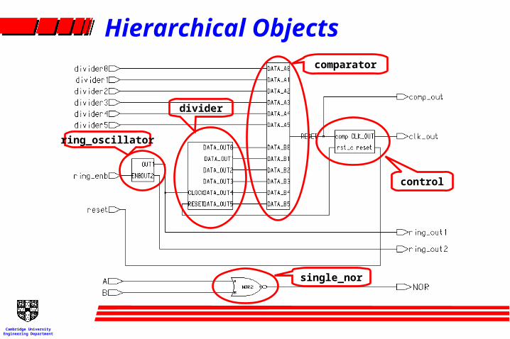
Hierarchical layout design Hierarchy - a methodology for creating
larger design from smaller design objects At lowest level objects are polygons, shapes
and paths (leaf cells), e.g. nor2, nand2 Inserted in a multi-tiered, hierarchical
design Designer controls visibility of detail Allows construction of libraries of commonly
used parts e.g. divider (based on count4) Permits re-use of designs in other projects
Cambridge University
Engineering Department
Hierarchical Objects
ring_oscillator
control
divider
comparator
single_nor
Cambridge University
Engineering Department
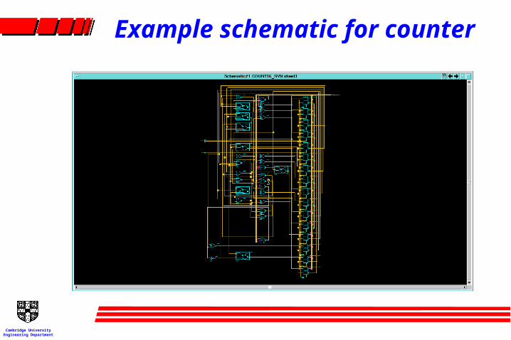
Example schematic for counter
Cambridge University
Engineering Department
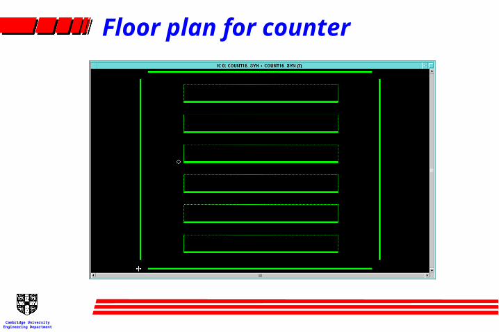
Floor plan for counter
Cambridge University
Engineering Department
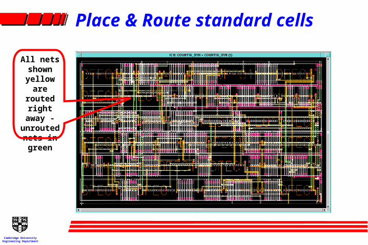
Place & Route standard cells
All nets shown
yellow are routed
right away - unrouted
nets in green
Cambridge University
Engineering Department
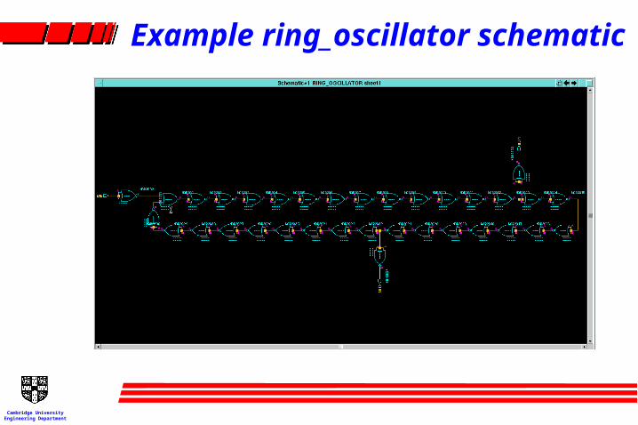
Example ring_oscillator schematic
Cambridge University
Engineering Department
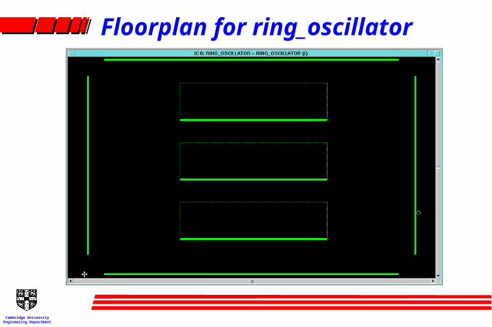
Floorplan for ring_oscillator
Cambridge University
Engineering Department
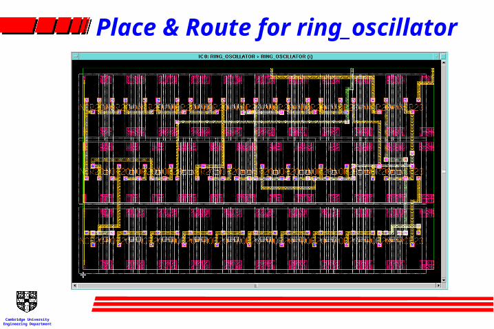
Place & Route for ring_oscillator
Cambridge University
Engineering Department
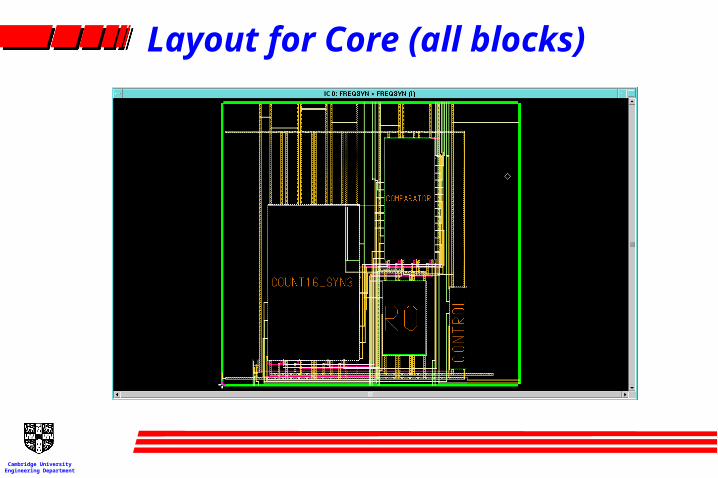
Layout for Core (all blocks)
Cambridge University
Engineering Department
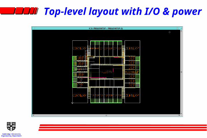
Top-level layout with I/O & power
Cambridge University
Engineering Department
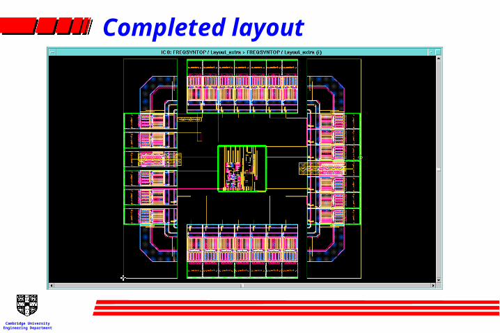
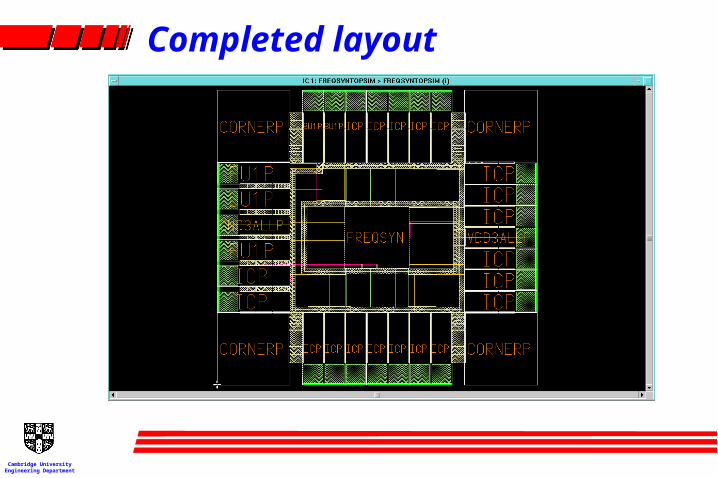
Completed layout
Cambridge University
Engineering Department
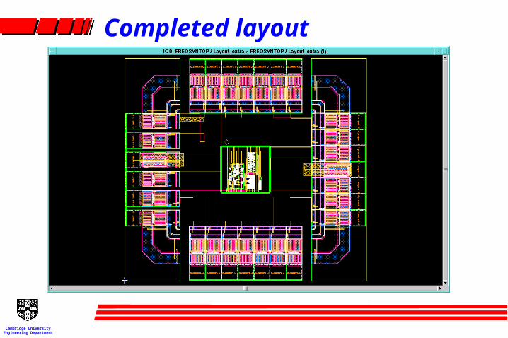
Completed layout
Cambridge University
Engineering Department
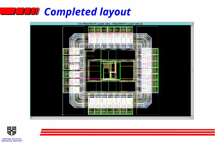
Completed layout
Cambridge University
Engineering Department
Completed layout

Cambridge University
Engineering Department
The End - 2009
Cambridge University
Engineering Department
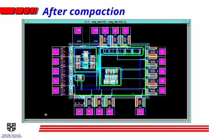
After compaction
Cambridge University
Engineering Department
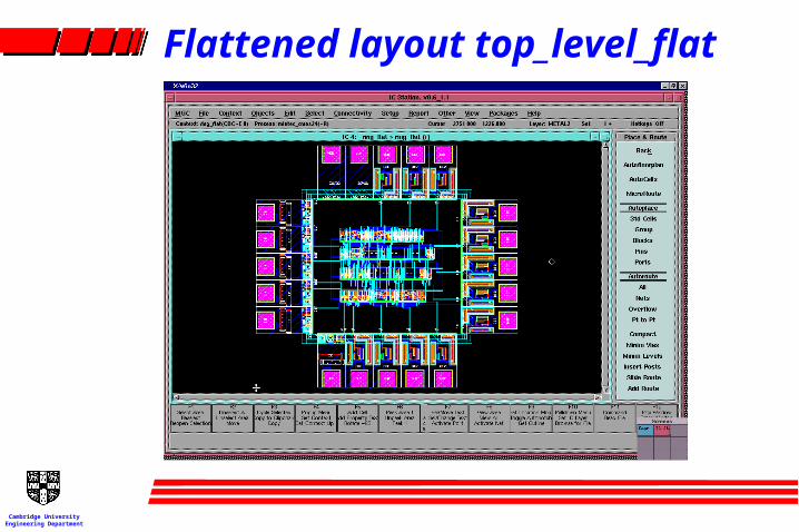
Flattened layout top_level_flat