Embed Size (px)
Citation preview
Birck Nanotechnology Center
Vladimir M. Shalaev
Purdue University
Birck Nanotechnology Center
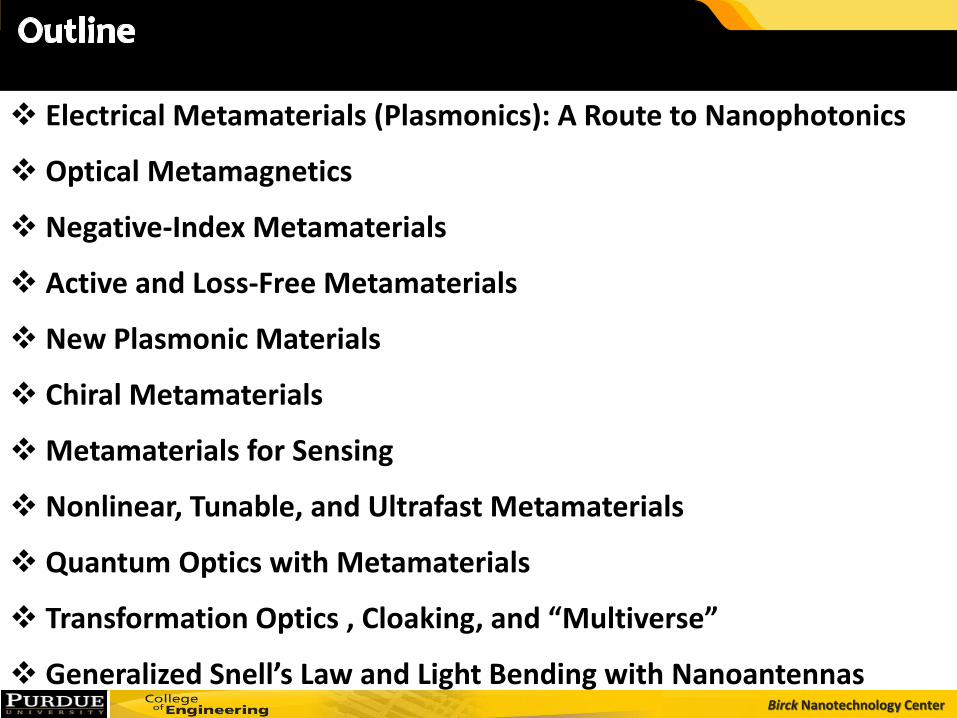
Electrical Metamaterials (Plasmonics): A Route to Nanophotonics
Optical Metamagnetics
Negative-Index Metamaterials
Active and Loss-Free Metamaterials
New Plasmonic Materials
Chiral Metamaterials
Metamaterials for Sensing
Nonlinear, Tunable, and Ultrafast Metamaterials
Quantum Optics with Metamaterials
Transformation Optics , Cloaking, and “Multiverse”
Generalized Snell’s Law and Light Bending with Nanoantennas
Birck Nanotechnology Center
3
Birck Nanotechnology Center
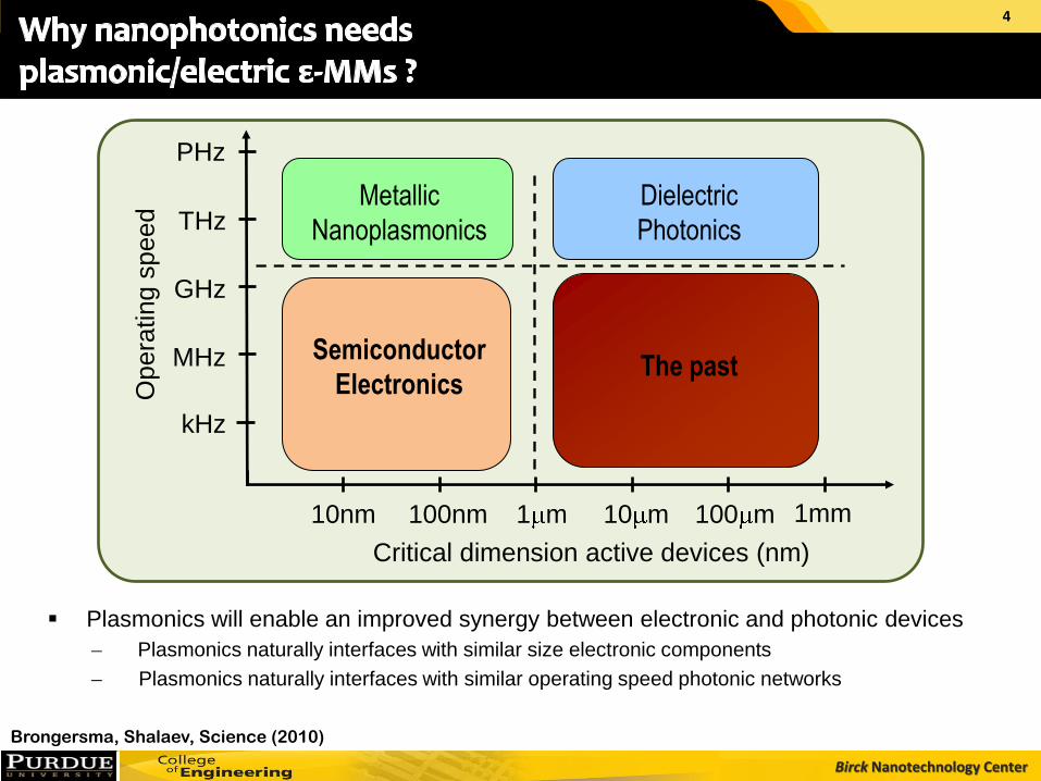
4
Plasmonics will enable an improved synergy between electronic and photonic devices
Plasmonics naturally interfaces with similar size electronic components
Plasmonics naturally interfaces with similar operating speed photonic networks
Brongersma, Shalaev, Science (2010)
Critical dimension active devices (nm)
Opera
ting s
peed
THz
GHz
MHz
kHz
10nm 100nm 1 m 10 m 1mm 100 m
Semiconductor
Electronics
Metallic
Nanoplasmonics
Dielectric
Photonics
The past
PHz
Birck Nanotechnology Center
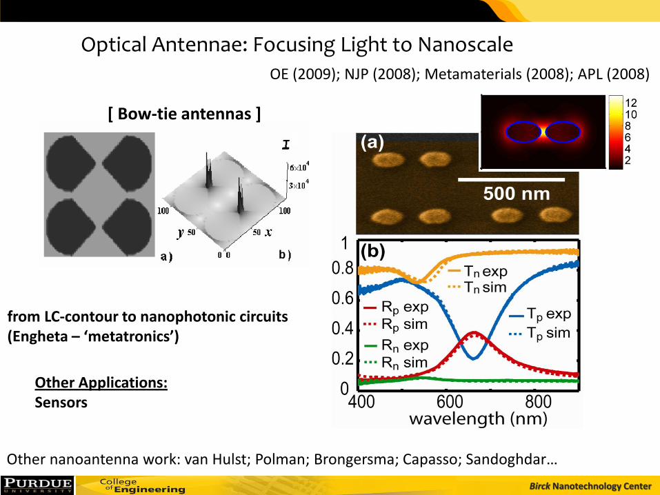
Optical Antennae: Focusing Light to Nanoscale
[ Bow-tie antennas ]
Other Applications: Sensors
from LC-contour to nanophotonic circuits (Engheta – ‘metatronics’)
Other nanoantenna work: van Hulst; Polman; Brongersma; Capasso; Sandoghdar…
OE (2009); NJP (2008); Metamaterials (2008); APL (2008)
Birck Nanotechnology Center
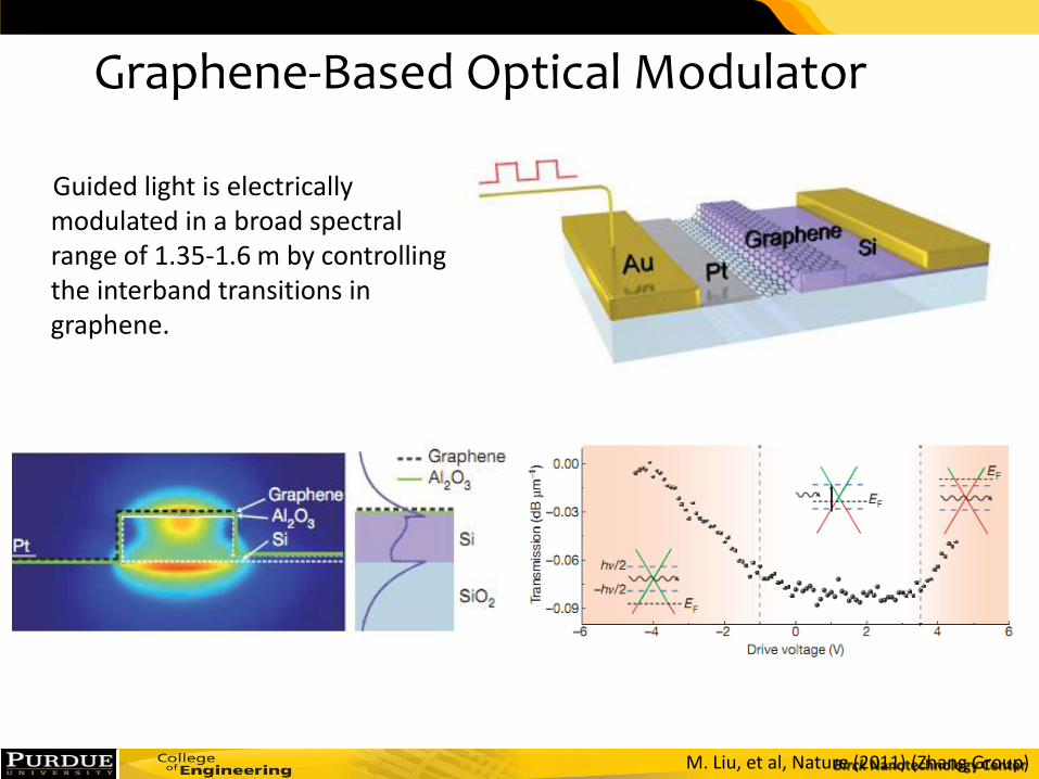
Graphene-Based Optical Modulator
M. Liu, et al, Nature (2011) (Zhang Group)
Guided light is electrically modulated in a broad spectral range of 1.35-1.6 m by controlling the interband transitions in graphene.
Birck Nanotechnology Center
d)
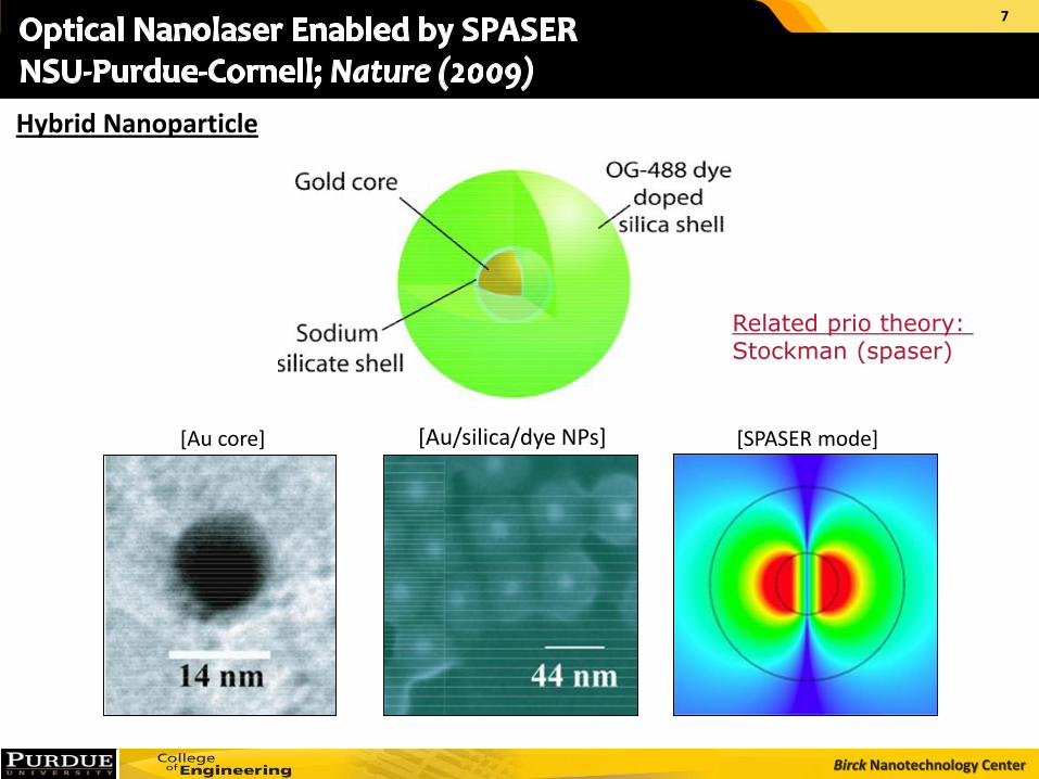
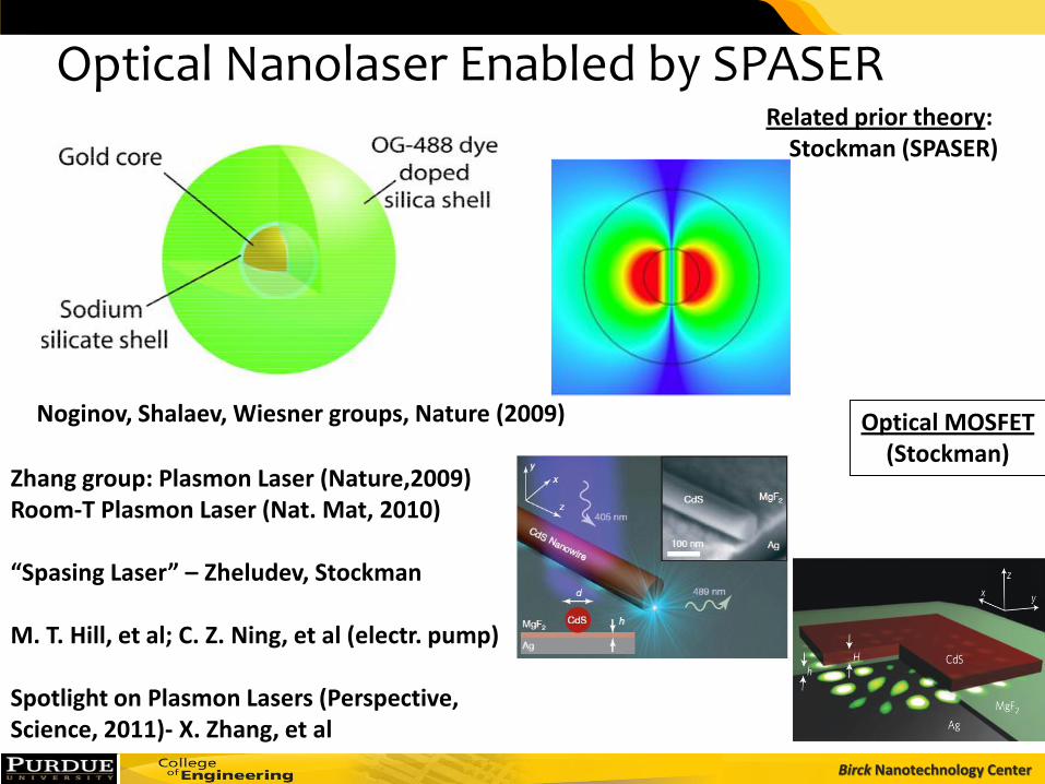
[Au core] [Au/silica/dye NPs] [SPASER mode]
Related prio theory: Stockman (spaser)
Hybrid Nanoparticle
7
Birck Nanotechnology Center
0
100
200
300
400
500
600
700
0 0.005 0.01 0.015 0.02 0.025
Em
issi
on
(re
l. u
nits
)Pumping (J)
Absorbed pumping per nanoparticle (10 -13 J)
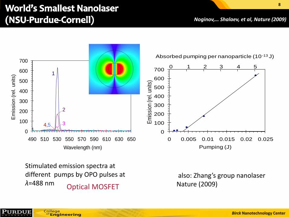
1 2 3 4 50
0
100
200
300
400
500
600
700
490 510 530 550 570 590 610 630 650
Em
issio
n (re
l. u
nits)
Wavelength (nm)
1
2
34,5
Stimulated emission spectra at different pumps by OPO pulses at λ=488 nm
Noginov,… Shalaev, et al, Nature (2009)
also: Zhang’s group nanolaser Nature (2009) Optical MOSFET
8
Birck Nanotechnology Center
Optical Nanolaser Enabled by SPASER Related prior theory:
Stockman (SPASER)
Zhang group: Plasmon Laser (Nature,2009) Room-T Plasmon Laser (Nat. Mat, 2010) “Spasing Laser” – Zheludev, Stockman M. T. Hill, et al; C. Z. Ning, et al (electr. pump) Spotlight on Plasmon Lasers (Perspective, Science, 2011)- X. Zhang, et al
Optical MOSFET (Stockman)
Noginov, Shalaev, Wiesner groups, Nature (2009)
Birck Nanotechnology Center Birck Nanotechnology Center
Birck Nanotechnology Center
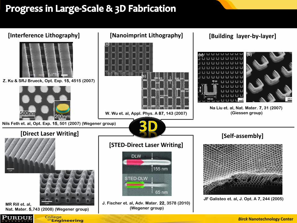
[Interference Lithography]
Z. Ku & SRJ Brueck, Opt. Exp. 15, 4515 (2007)
Nils Feth et. al, Opt. Exp. 15, 501 (2007) (Wegener group)
[Direct Laser Writing]
MR Rill et. al,
Nat. Mater. 5,743 (2008) (Wegener group)
[STED-Direct Laser Writing]
J. Fischer et. al, Adv. Mater. 22, 3578 (2010)
(Wegener group)
[Self-assembly]
Na Liu et. al, Nat. Mater. 7, 31 (2007)
(Giessen group)
JF Galisteo et. al, J. Opt. A 7, 244 (2005)
[Building layer-by-layer] [Nanoimprint Lithography]
W. Wu et. al, Appl. Phys. A 87, 143 (2007)
Birck Nanotechnology Center
12
Birck Nanotechnology Center
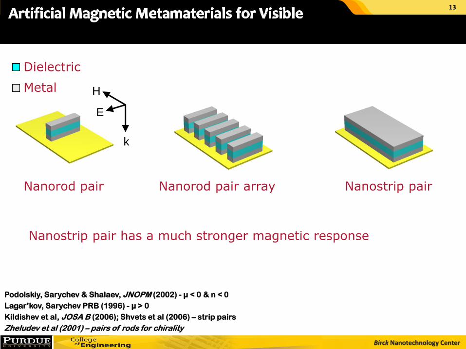
E
H
k
Dielectric
Metal
Nanorod pair Nanorod pair array Nanostrip pair
Nanostrip pair has a much stronger magnetic response
Podolskiy, Sarychev & Shalaev, JNOPM (2002) - µ < 0 & n < 0
Lagar’kov, Sarychev PRB (1996) - µ > 0
Kildishev et al, JOSA B (2006); Shvets et al (2006) – strip pairs
Zheludev et al (2001) – pairs of rods for chirality
13
Birck Nanotechnology Center
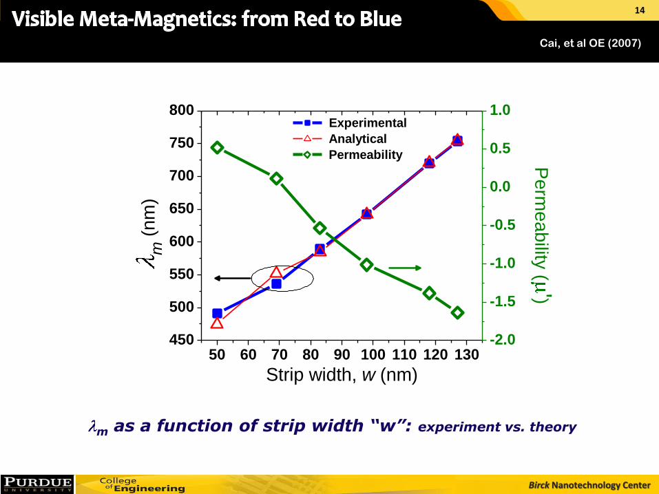
m as a function of strip width “w”: experiment vs. theory
50 60 70 80 90 100 110 120 130450
500
550
600
650
700
750
800 Experimental
Analytical
Permeability
Strip width, w (nm)
m (
nm
)
-2.0
-1.5
-1.0
-0.5
0.0
0.5
1.0P
erm
eability
(')
Cai, et al OE (2007)
14
Birck Nanotechnology Center
15

Birck Nanotechnology Center
Sir Arthur Schuster Sir Horace Lamb
L. I. Mandel’stam
V. G. Veselago
Sir John Pendry
… energy can be carried forward at the group velocity
but in a direction that is anti-parallel to the phase
velocity…
Schuster, 1904
Negative refraction and backward propagation of
waves
Mandel’stam, 1945
Left-handed materials: the electrodynamics of substances
with simultaneously negative values of and
Veselago, 1968
Pendry, the one who whipped up the recent boom
of NIM researches
Perfect lens (2000)
EM cloaking (2006) Others: Sivukhin. Agranovich,…
16
Birck Nanotechnology Center
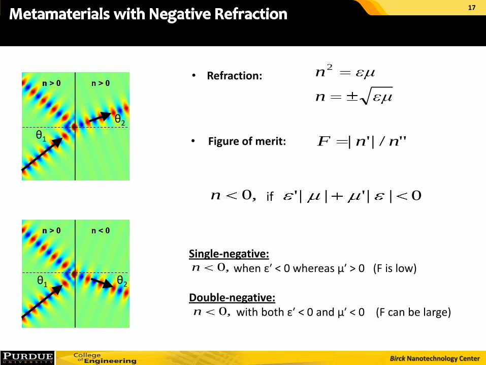
Single-negative: when ε′ < 0 whereas μ′ > 0 (F is low) Double-negative: with both ε′ < 0 and μ′ < 0 (F can be large)
if ,0n
• Refraction:
• Figure of merit: θ1
θ2
θ1 θ2
"/|'| nnF
εμn
εμn2
0 ||' ||'
,0n
,0n
17
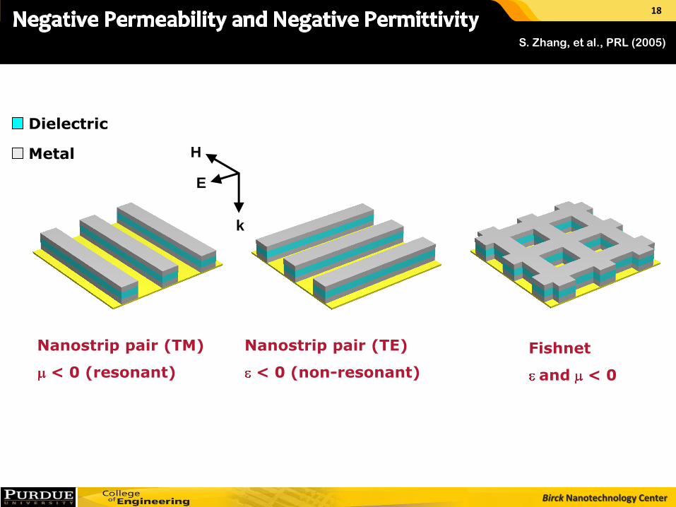
Birck Nanotechnology Center
E
H
k
Dielectric
Metal
Nanostrip pair (TM)
< 0 (resonant)
Nanostrip pair (TE)
< 0 (non-resonant)
Fishnet
and < 0
S. Zhang, et al., PRL (2005)
18
Birck Nanotechnology Center
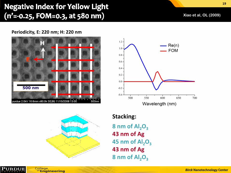
Periodicity, E: 220 nm; H: 220 nm
Stacking:
8 nm of Al2O3 43 nm of Ag 45 nm of Al2O3
43 nm of Ag 8 nm of Al2O3
E
H
500 nm
Xiao et al, OL (2009)
19
Birck Nanotechnology Center
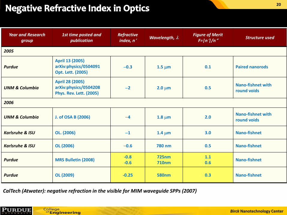
Year and Research group
1st time posted and publication
Refractive index, n
Wavelength, Figure of Merit
F=|n |/n Structure used
2005
Purdue
April 13 (2005) arXiv:physics/0504091 Opt. Lett. (2005)
0.3 1.5 m 0.1 Paired nanorods
UNM & Columbia
April 28 (2005) arXiv:physics/0504208 Phys. Rev. Lett. (2005)
2 2.0 m 0.5 Nano-fishnet with round voids
2006
UNM & Columbia J. of OSA B (2006) 4 1.8 m 2.0 Nano-fishnet with round voids
Karlsruhe & ISU OL. (2006) 1 1.4 m 3.0 Nano-fishnet
Karlsruhe & ISU OL (2006) 0.6 780 nm 0.5 Nano-fishnet
Purdue MRS Bulletin (2008) -0.8 -0.6
725nm 710nm
1.1 0.6
Nano-fishnet
Purdue OL (2009) -0.25 580nm 0.3 Nano-fishnet
CalTech (Atwater): negative refraction in the visible for MIM waveguide SPPs (2007)
20
Birck Nanotechnology Center
Birck Nanotechnology Center
Birck Nanotechnology Center
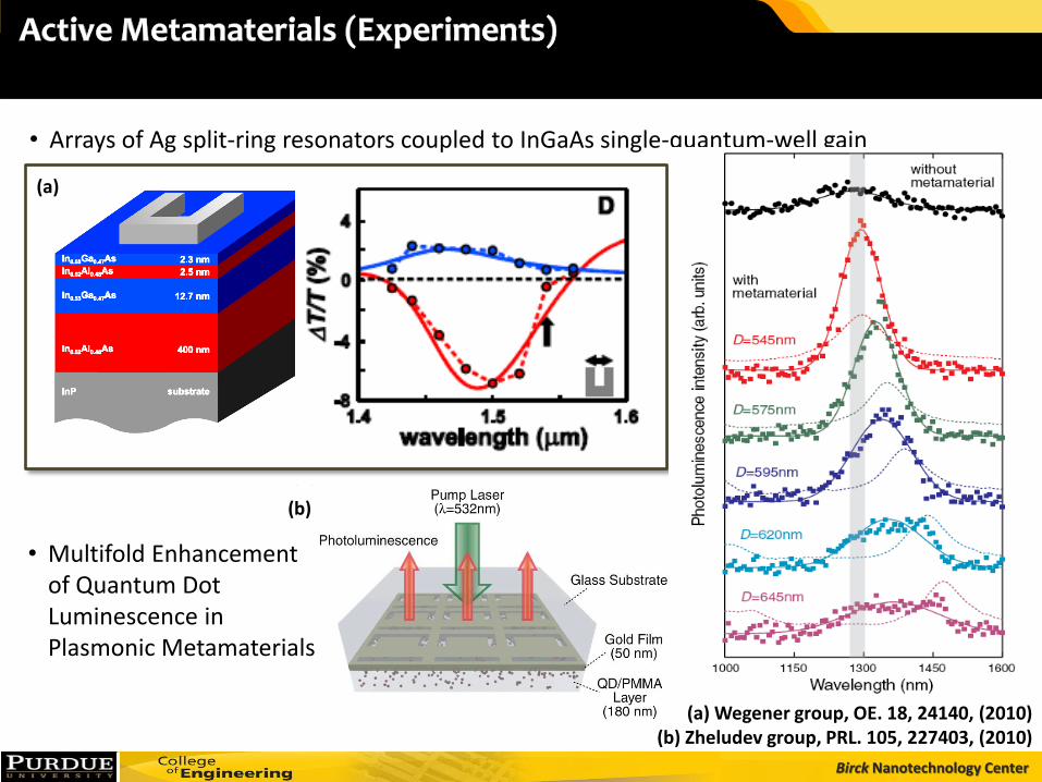
(a) Wegener group, OE. 18, 24140, (2010) (b) Zheludev group, PRL. 105, 227403, (2010)
• Arrays of Ag split-ring resonators coupled to InGaAs single-quantum-well gain
• Multifold Enhancement of Quantum Dot Luminescence in Plasmonic Metamaterials
(a)
(b)
Birck Nanotechnology Center
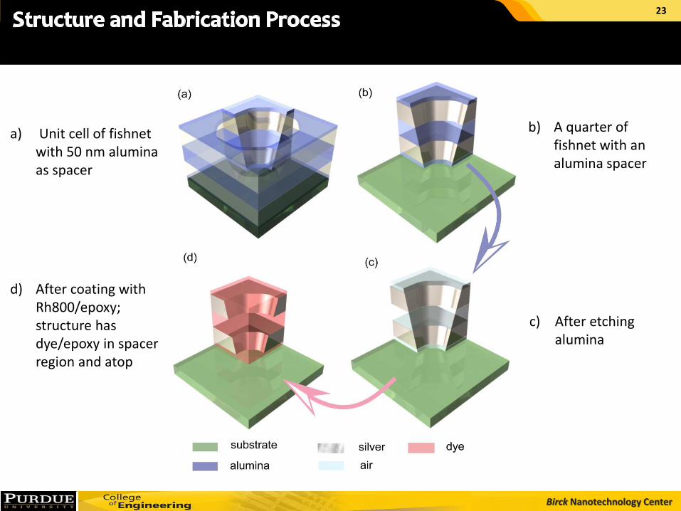
a) Unit cell of fishnet with 50 nm alumina as spacer
b) A quarter of fishnet with an alumina spacer
c) After etching alumina
d) After coating with Rh800/epoxy; structure has dye/epoxy in spacer region and atop
23
Birck Nanotechnology Center
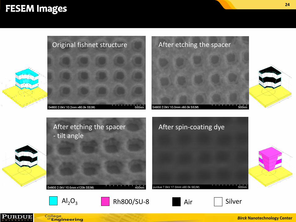
Al2O3 Rh800/SU-8
Original fishnet structure After etching the spacer
After etching the spacer - tilt angle
After spin-coating dye
Air Silver
24
Birck Nanotechnology Center
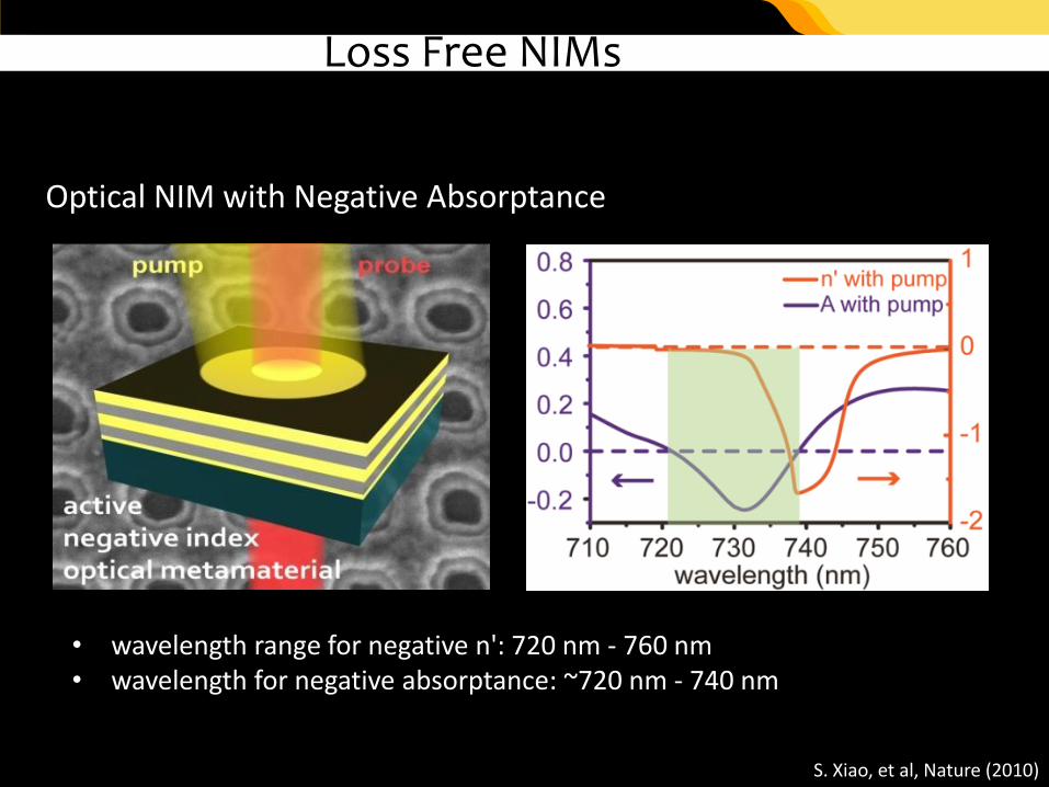
Loss Free NIMs
S. Xiao, et al, Nature (2010)
Optical NIM with Negative Absorptance
• wavelength range for negative n': 720 nm - 760 nm • wavelength for negative absorptance: ~720 nm - 740 nm
Birck Nanotechnology Center
Toward Better Materials for
Negative Refraction (Boltasseva group)
Birck Nanotechnology Center
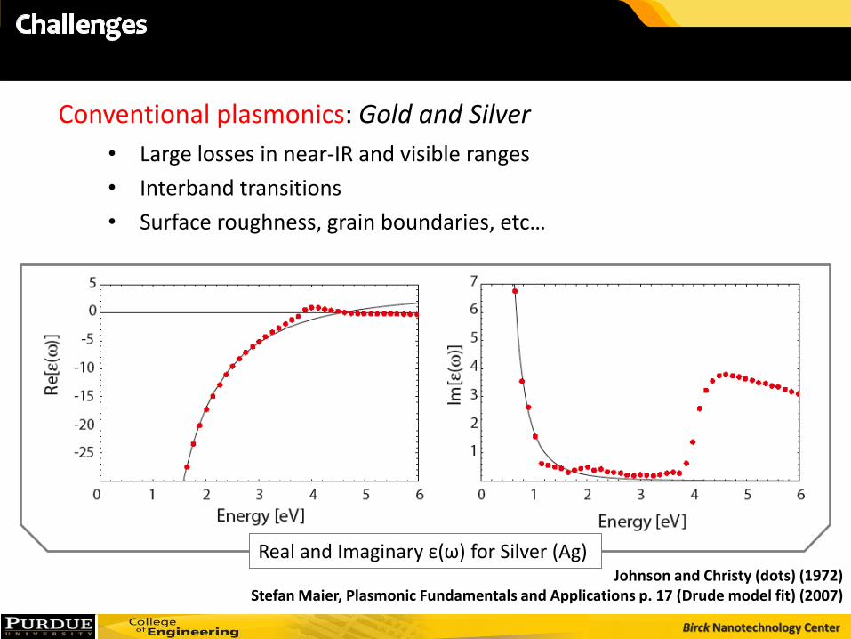
Conventional plasmonics: Gold and Silver
• Large losses in near-IR and visible ranges
• Interband transitions
• Surface roughness, grain boundaries, etc…
Real and Imaginary ε(ω) for Silver (Ag) Johnson and Christy (dots) (1972)
Stefan Maier, Plasmonic Fundamentals and Applications p. 17 (Drude model fit) (2007)
Birck Nanotechnology Center
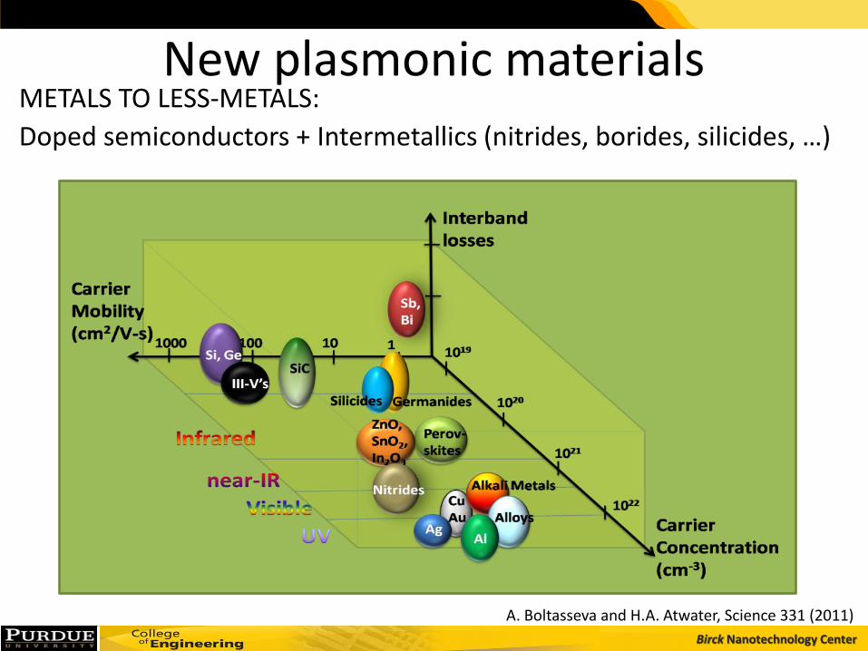
METALS TO LESS-METALS:
Doped semiconductors + Intermetallics (nitrides, borides, silicides, …)
New plasmonic materials
A. Boltasseva and H.A. Atwater, Science 331 (2011)
Birck Nanotechnology Center
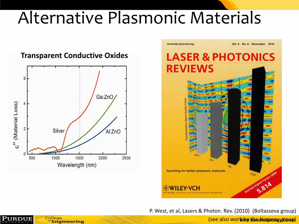
Alternative Plasmonic Materials
P. West, et al, Lasers & Photon. Rev. (2010) (Boltasseva group)
(see also work by the Noginov group)
Transparent Conductive Oxides
Birck Nanotechnology Center
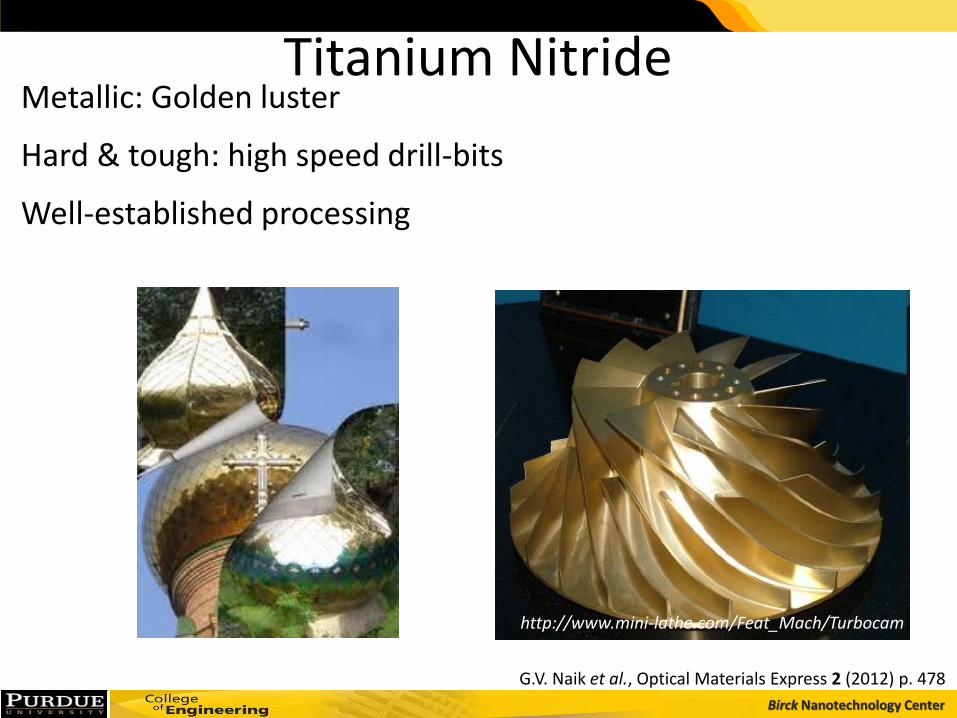
Metallic: Golden luster Hard & tough: high speed drill-bits Well-established processing
Titanium Nitride
G.V. Naik et al., Optical Materials Express 2 (2012) p. 478
http://www.mini-lathe.com/Feat_Mach/Turbocam
Birck Nanotechnology Center
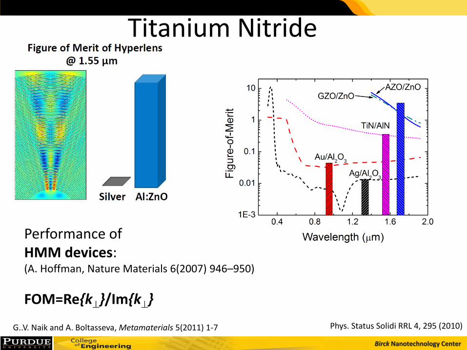
Titanium Nitride
Performance of HMM devices: (A. Hoffman, Nature Materials 6(2007) 946–950)
FOM=Re{k }/Im{k }
Phys. Status Solidi RRL 4, 295 (2010) G..V. Naik and A. Boltasseva, Metamaterials 5(2011) 1-7
Birck Nanotechnology Center
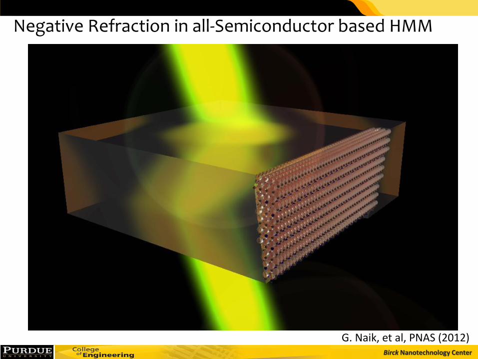
Negative Refraction in all-Semiconductor based HMM
G. Naik, et al, PNAS (2012)
Birck Nanotechnology Center
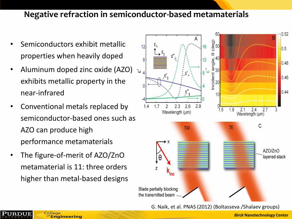
Negative refraction in semiconductor-based metamaterials
• Semiconductors exhibit metallic
properties when heavily doped
• Aluminum doped zinc oxide (AZO)
exhibits metallic property in the
near-infrared
• Conventional metals replaced by
semiconductor-based ones such as
AZO can produce high
performance metamaterials
• The figure-of-merit of AZO/ZnO
metamaterial is 11: three orders
higher than metal-based designs
G. Naik, et al. PNAS (2012) (Boltasseva /Shalaev groups)
Birck Nanotechnology Center Birck Nanotechnology Center
Birck Nanotechnology Center
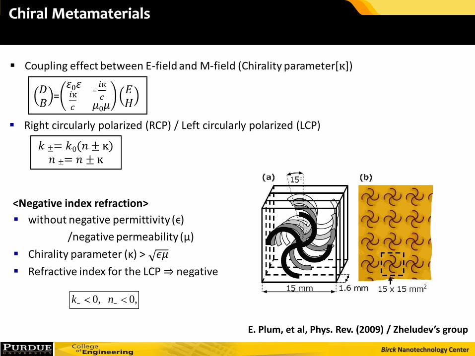
0, 0,k n
Right circularly polarized (RCP) / Left circularly polarized (LCP)
<Negative index refraction>
E. Plum, et al, Phys. Rev. (2009) / Zheludev’s group
Birck Nanotechnology Center
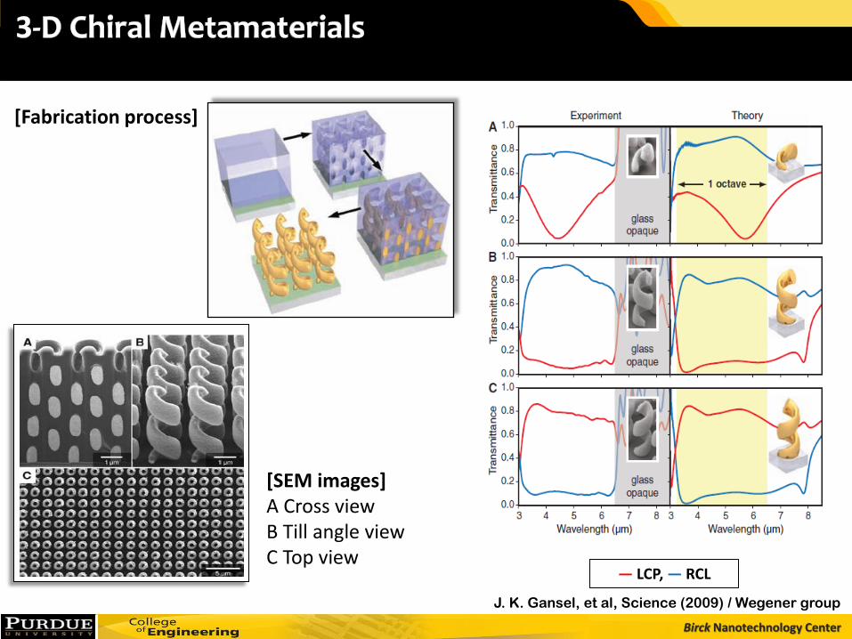
J. K. Gansel, et al, Science (2009) / Wegener group
— LCP, — RCL
[Fabrication process]
[SEM images] A Cross view B Till angle view C Top view
Birck Nanotechnology Center Birck Nanotechnology Center
Birck Nanotechnology Center
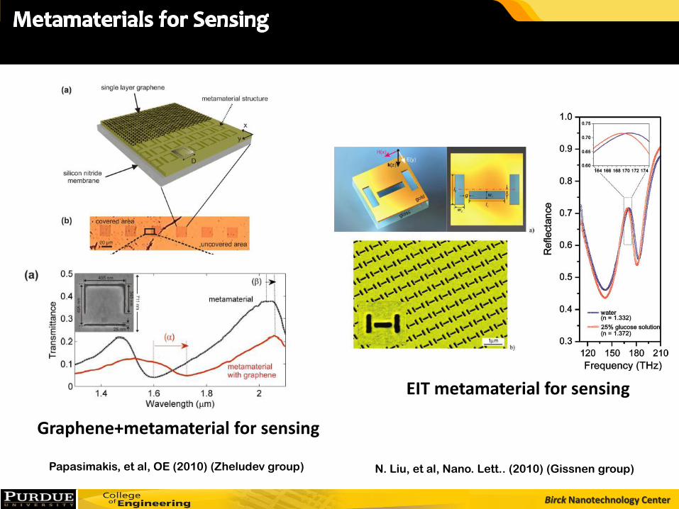
EIT metamaterial for sensing
Graphene+metamaterial for sensing
Papasimakis, et al, OE (2010) (Zheludev group) N. Liu, et al, Nano. Lett.. (2010) (Gissnen group)
Birck Nanotechnology Center
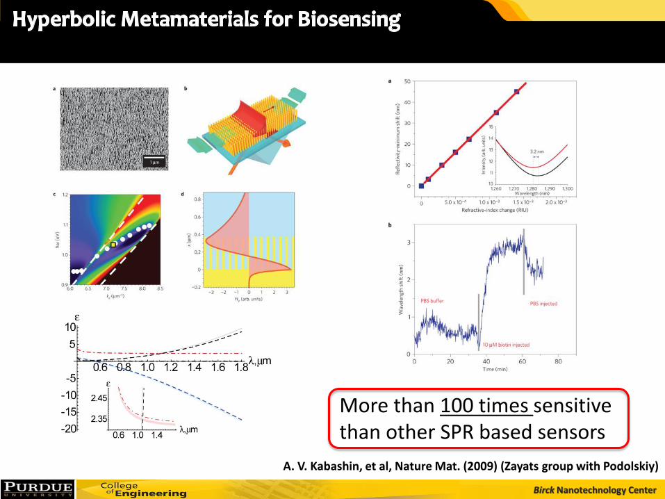
More than 100 times sensitive than other SPR based sensors
A. V. Kabashin, et al, Nature Mat. (2009) (Zayats group with Podolskiy)
Birck Nanotechnology Center
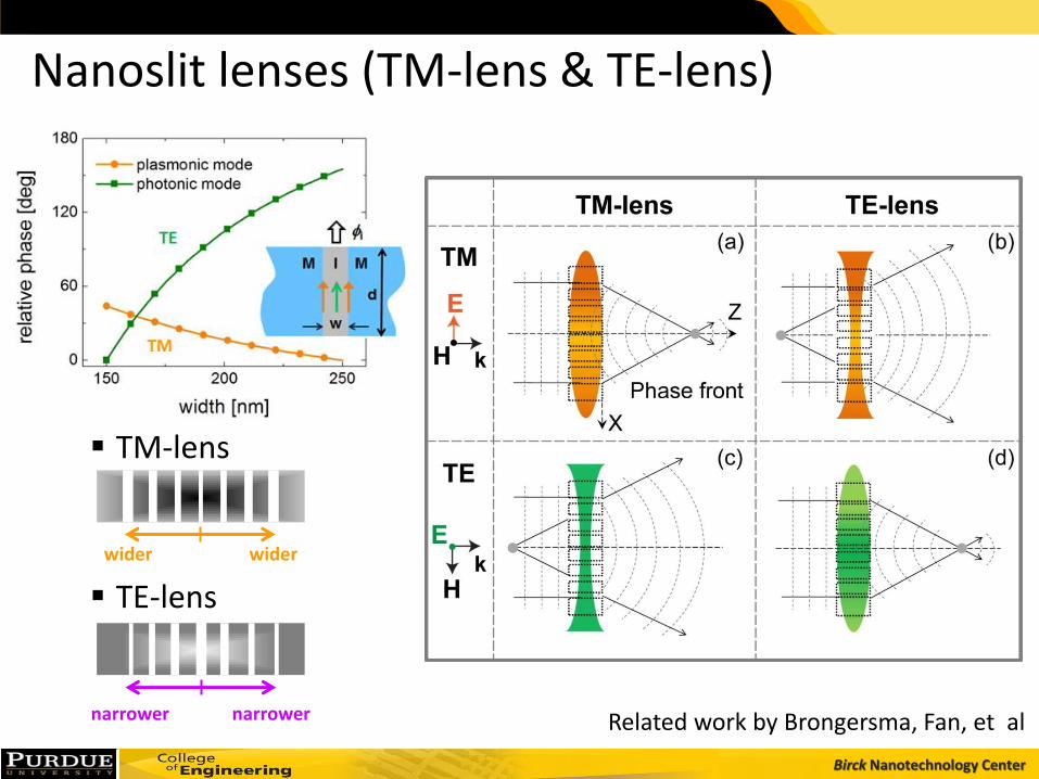
Nanoslit Lenses
Key author: Satoshi Ishii (see his poster)
Birck Nanotechnology Center
Nanoslit lenses (TM-lens & TE-lens)
TM-lens
TE-lens
wider wider
narrower narrower Related work by Brongersma, Fan, et al
Birck Nanotechnology Center
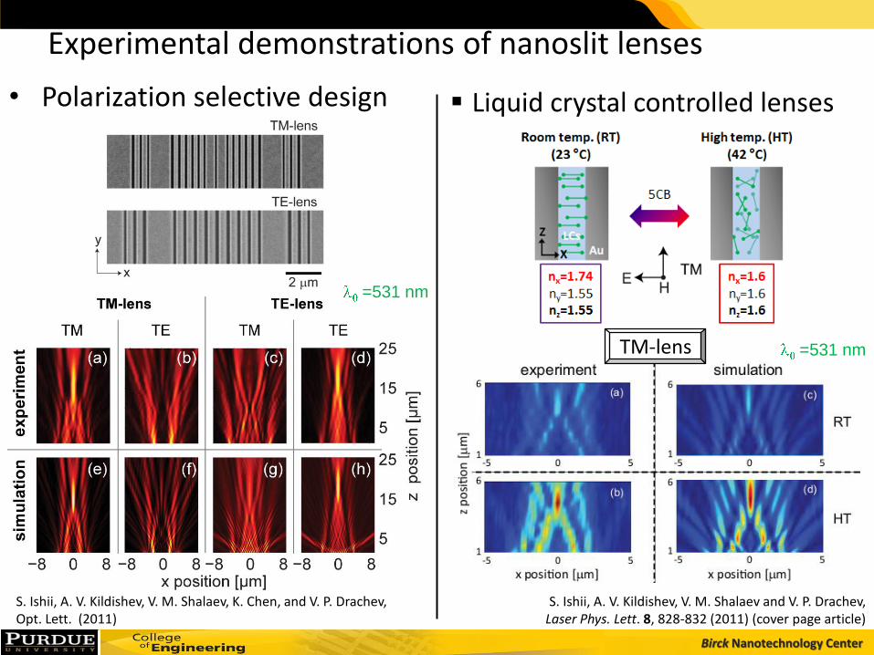
Experimental demonstrations of nanoslit lenses
S. Ishii, A. V. Kildishev, V. M. Shalaev and V. P. Drachev, Laser Phys. Lett. 8, 828-832 (2011) (cover page article)
=531 nm
=531 nm
S. Ishii, A. V. Kildishev, V. M. Shalaev, K. Chen, and V. P. Drachev, Opt. Lett. (2011)
• Polarization selective design Liquid crystal controlled lenses
TM-lens
Birck Nanotechnology Center
Negative-Index Metamaterials
and Nonlinear Optics
Birck Nanotechnology Center
44
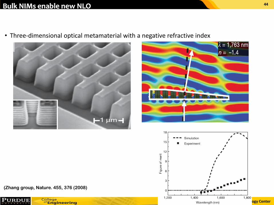
(Zhang group, Nature. 455, 376 (2008)
• Three-dimensional optical metamaterial with a negative refractive index
Birck Nanotechnology Center 45
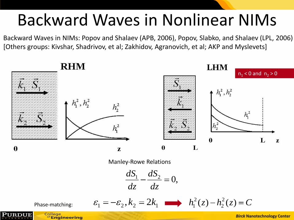
Backward Waves in Nonlinear NIMs
Backward Waves in NIMs: Popov and Shalaev (APB, 2006), Popov, Slabko, and Shalaev (LPL, 2006) [Others groups: Kivshar, Shadrivov, et al; Zakhidov, Agranovich, et al; AKP and Myslevets]
02
2
2
2
2
2
1
1
1
dz
dhk
dz
dhkCzhzh )()( 2
2
2
1
Manley-Rowe Relations
,021
dz
dS
dz
dS
Czhzh )()( 2
2
2
11221 2, kkPhase-matching:
n1 < 0 and n2 > 0
Birck Nanotechnology Center
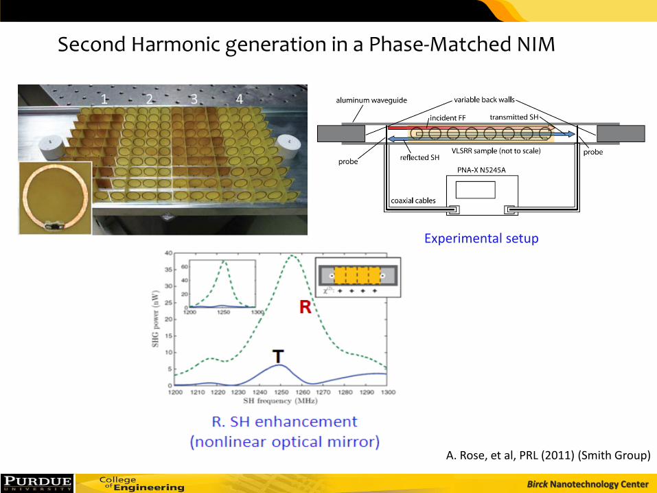
Second Harmonic generation in a Phase-Matched NIM
A. Rose, et al, PRL (2011) (Smith Group)
Experimental setup
Birck Nanotechnology Center
47
Birck Nanotechnology Center
Birck Nanotechnology Center
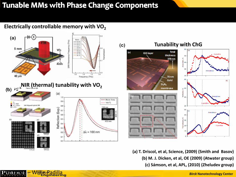
(a) T. Driscol, et al, Science, (2009) (Smith and Basov)
(b) M. J. Dicken, et al, OE (2009) (Atwater group)
(c) Sámson, et al, APL, (2010) (Zheludev group)
NIR (thermal) tunability with VO2
Tunability with ChG
(b)
(c)
Electrically controllable memory with VO2
(a)
THz range – Willie Padilla
Birck Nanotechnology Center
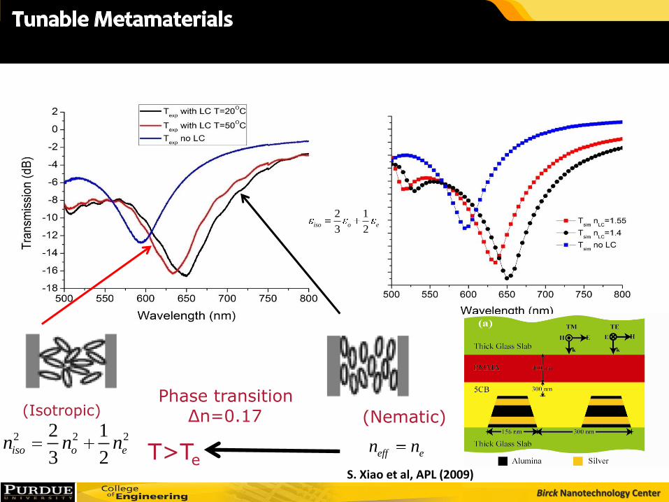
2 1
3 2iso o e
'
Phase transition Δn=0.17
eff en n
(Nematic) (Isotropic)
T>Te
2 2 22 1
3 2iso o en n n
S. Xiao et al, APL (2009)
Birck Nanotechnology Center
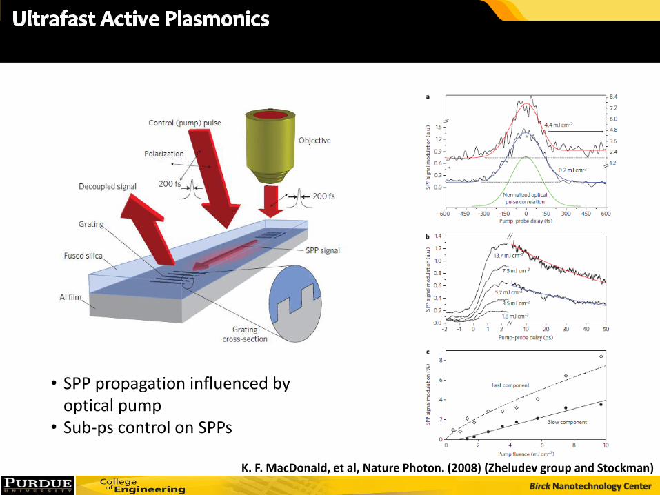
K. F. MacDonald, et al, Nature Photon. (2008) (Zheludev group and Stockman)
• SPP propagation influenced by optical pump
• Sub-ps control on SPPs
Birck Nanotechnology Center
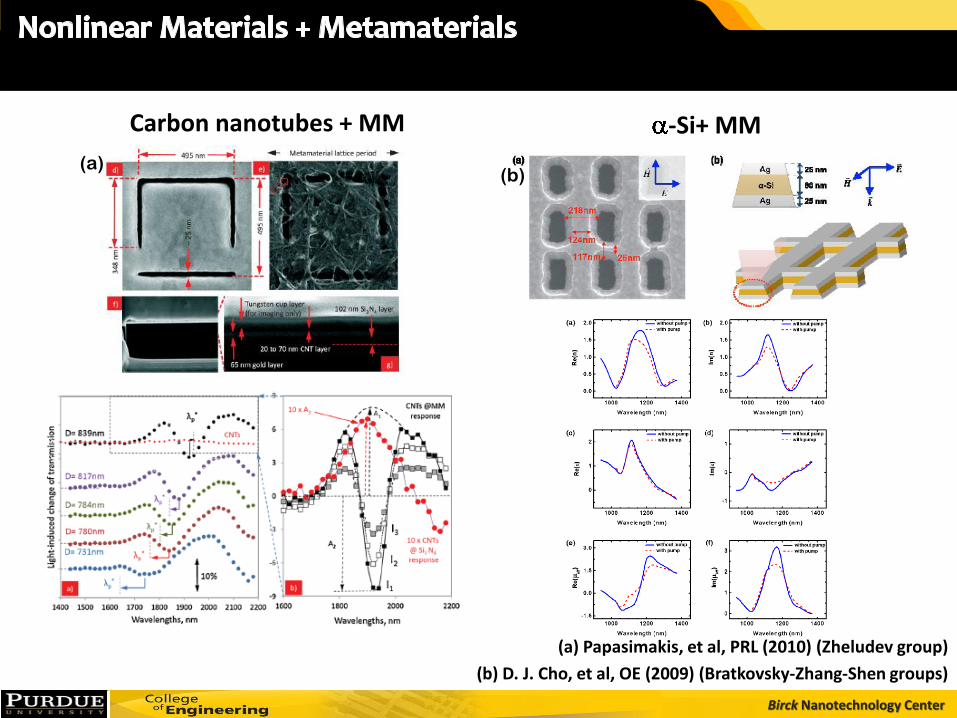
Carbon nanotubes + MM -Si+ MM
(a) Papasimakis, et al, PRL (2010) (Zheludev group)
(b) D. J. Cho, et al, OE (2009) (Bratkovsky-Zhang-Shen groups)
(a) (b)
Birck Nanotechnology Center
J.-Y. Kim, G. V. Naik, Z. Jacob, V. P. Drachev,
Alexandra Boltasseva, Evgenii E. Narimanov and Vladimir M. Shalaev
52
Birck Nanotechnology Center
“Regular” dielectric
“Strongly Anisotropic” media
Special case of “Indefinite Media”, D.Smith et al, 2003
53
Birck Nanotechnology Center
Unlimited wavenumbers
“Infinite” refractive index
No diffraction limit for imaging
Z. Jacob et. al, Opt. Express (2007), Hyperlens
54
Birck Nanotechnology Center
Unlimited wavenumbers
“Infinite” refractive index
No diffraction limit for imaging
HYPERLENS
Ag/ Al2O3 multilayers
Hyperlens
Theory : E.Narimanov et al, N. Engheta et at, 2006
Experiment : X. Zhang et al, 2007
55
Birck Nanotechnology Center
Hyperbolic dispersion supports high spatial wavevectors compared to vacuum
Large contribution to DOS from the “high k” states (think beyond imaging!)
εx > 0 εz > 0
εy < 0
[vacuum]
[metamaterial] (|k| unbounded)
56
Birck Nanotechnology Center
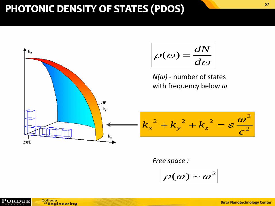
N(ω) - number of states with frequency below ω
d
dN)(
2)(
2
2222
ckkk zyx
Free space :
57
Birck Nanotechnology Center
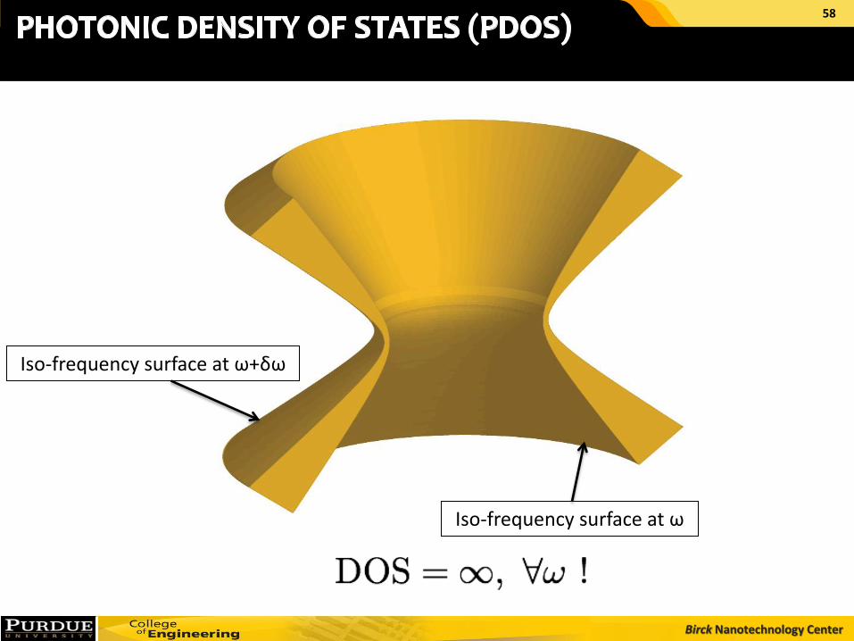
Iso-frequency surface at ω
Iso-frequency surface at ω+δω
58
Birck Nanotechnology Center
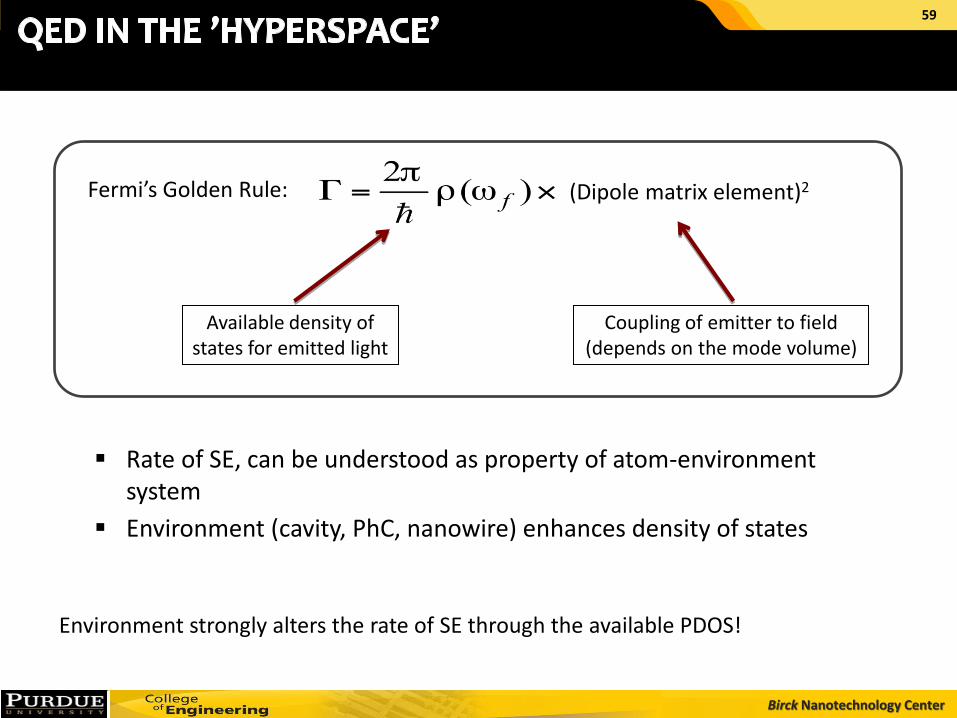
Rate of SE, can be understood as property of atom-environment system
Environment (cavity, PhC, nanowire) enhances density of states
(Dipole matrix element)2
Environment strongly alters the rate of SE through the available PDOS!
Fermi’s Golden Rule:
Available density of states for emitted light
Coupling of emitter to field (depends on the mode volume)
59
Birck Nanotechnology Center
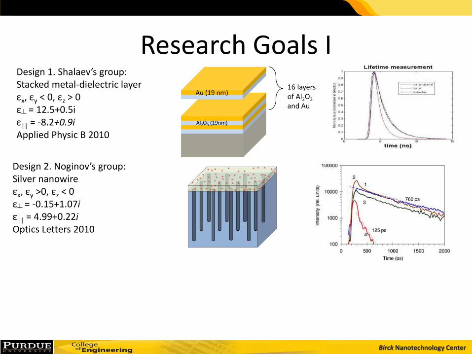
Research Goals I
Al2O3 (19nm)
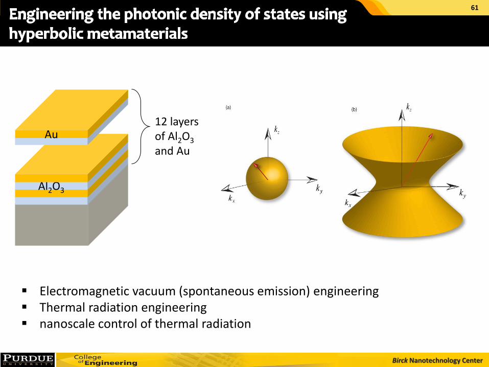
Au (19 nm) 16 layers of Al2O3 and Au
Design 1. Shalaev’s group: Stacked metal-dielectric layer εx, εy < 0, εz > 0 ε┴ = 12.5+0.5i ε|| = -8.2+0.9i Applied Physic B 2010
Design 2. Noginov’s group: Silver nanowire εx, εy >0, εz < 0 ε┴ = -0.15+1.07i ε|| = 4.99+0.22i Optics Letters 2010
Birck Nanotechnology Center
Al2O3
Au 12 layers of Al2O3 and Au
Electromagnetic vacuum (spontaneous emission) engineering Thermal radiation engineering nanoscale control of thermal radiation
61
Birck Nanotechnology Center
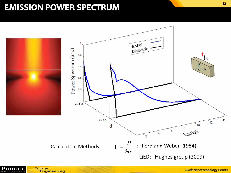
: Ford and Weber (1984)
QED: Hughes group (2009)
Calculation Methods:
62
Birck Nanotechnology Center
V. M. Shalaev, Transforming Light, Science, Oct. 17, 2008
63
Birck Nanotechnology Center
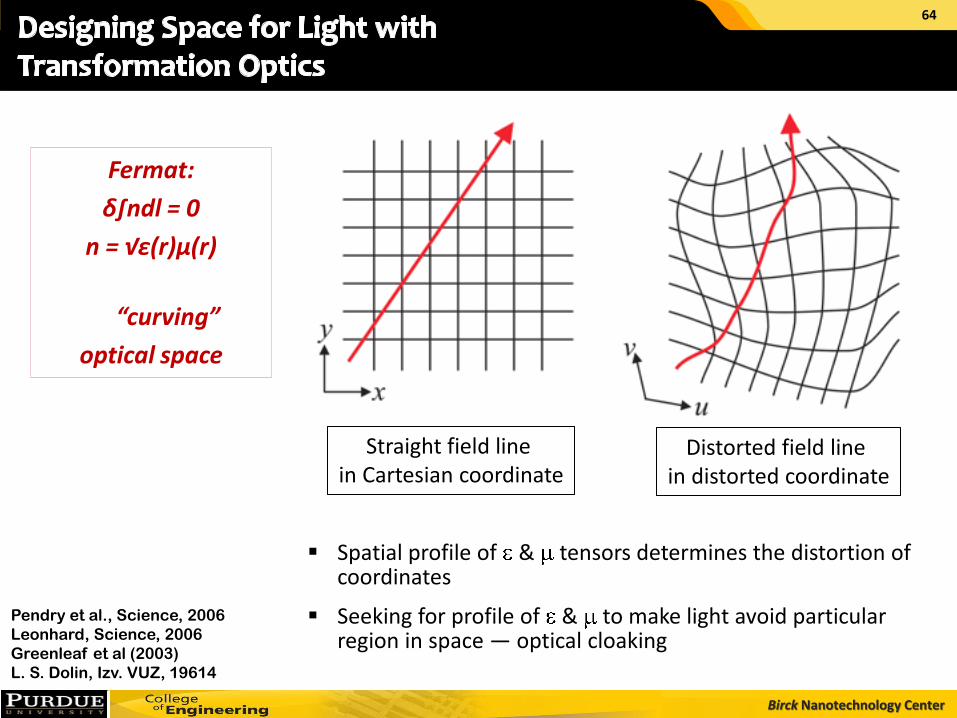
Spatial profile of & tensors determines the distortion of coordinates
Seeking for profile of & to make light avoid particular region in space — optical cloaking
Fermat:
δ∫ndl = 0
n = √ε(r)μ(r)
“curving”
optical space
Distorted field line in distorted coordinate
Straight field line in Cartesian coordinate
Pendry et al., Science, 2006
Leonhard, Science, 2006
Greenleaf et al (2003)
L. S. Dolin, Izv. VUZ, 19614
64
Birck Nanotechnology Center
Narimanov, Kildishev
65
Birck Nanotechnology Center
66
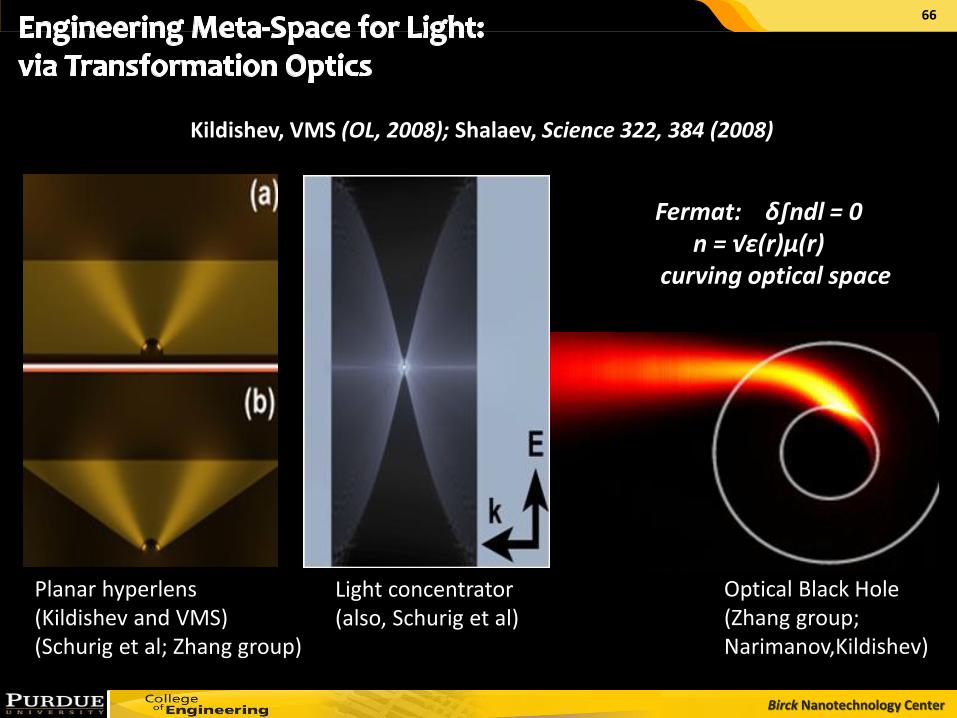
Kildishev, VMS (OL, 2008); Shalaev, Science 322, 384 (2008)
Optical Black Hole (Zhang group; Narimanov,Kildishev)
(b)
Fermat: δ∫ndl = 0 n = √ε(r)μ(r)
curving optical space
Planar hyperlens (Kildishev and VMS) (Schurig et al; Zhang group)
Light concentrator (also, Schurig et al)
Birck Nanotechnology Center
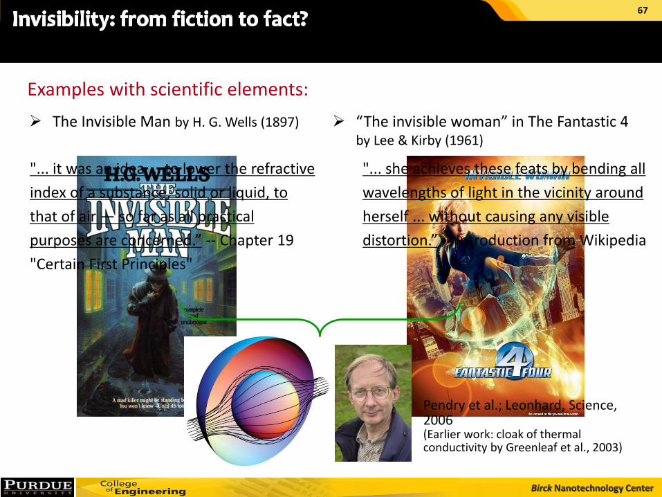
The Invisible Man by H. G. Wells (1897)
“The invisible woman” in The Fantastic 4 by Lee & Kirby (1961)
Examples with scientific elements:
"... it was an idea ... to lower the refractive
index of a substance, solid or liquid, to
that of air — so far as all practical
purposes are concerned.” -- Chapter 19
"Certain First Principles"
"... she achieves these feats by bending all
wavelengths of light in the vicinity around
herself ... without causing any visible
distortion.” -- Introduction from Wikipedia
Pendry et al.; Leonhard, Science, 2006 (Earlier work: cloak of thermal conductivity by Greenleaf et al., 2003)
67
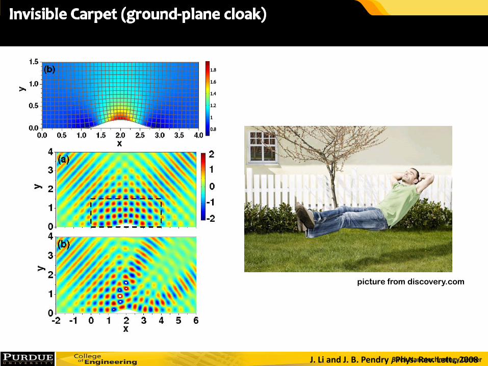
Birck Nanotechnology Center J. Li and J. B. Pendry , Phys. Rev. Lett., 2008
picture from discovery.com
Birck Nanotechnology Center
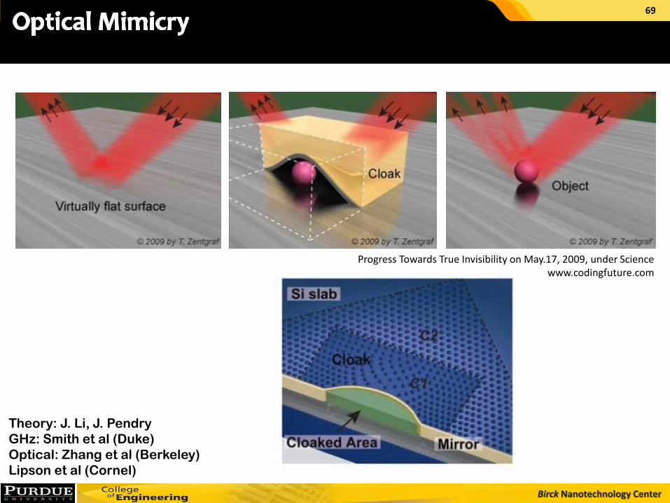
Progress Towards True Invisibility on May.17, 2009, under Science www.codingfuture.com
Theory: J. Li, J. Pendry
GHz: Smith et al (Duke)
Optical: Zhang et al (Berkeley)
Lipson et al (Cornel)
69
Birck Nanotechnology Center
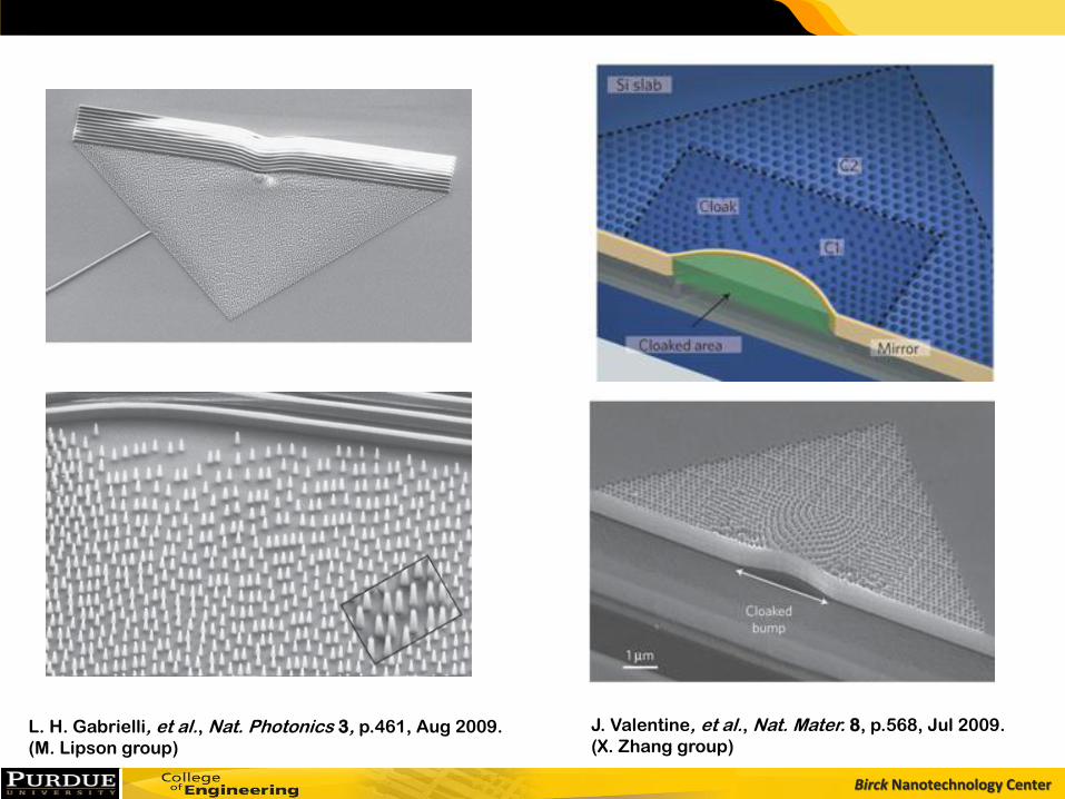
L. H. Gabrielli, et al., Nat. Photonics 3, p.461, Aug 2009.
(M. Lipson group)
J. Valentine, et al., Nat. Mater. 8, p.568, Jul 2009.
(X. Zhang group)
Birck Nanotechnology Center
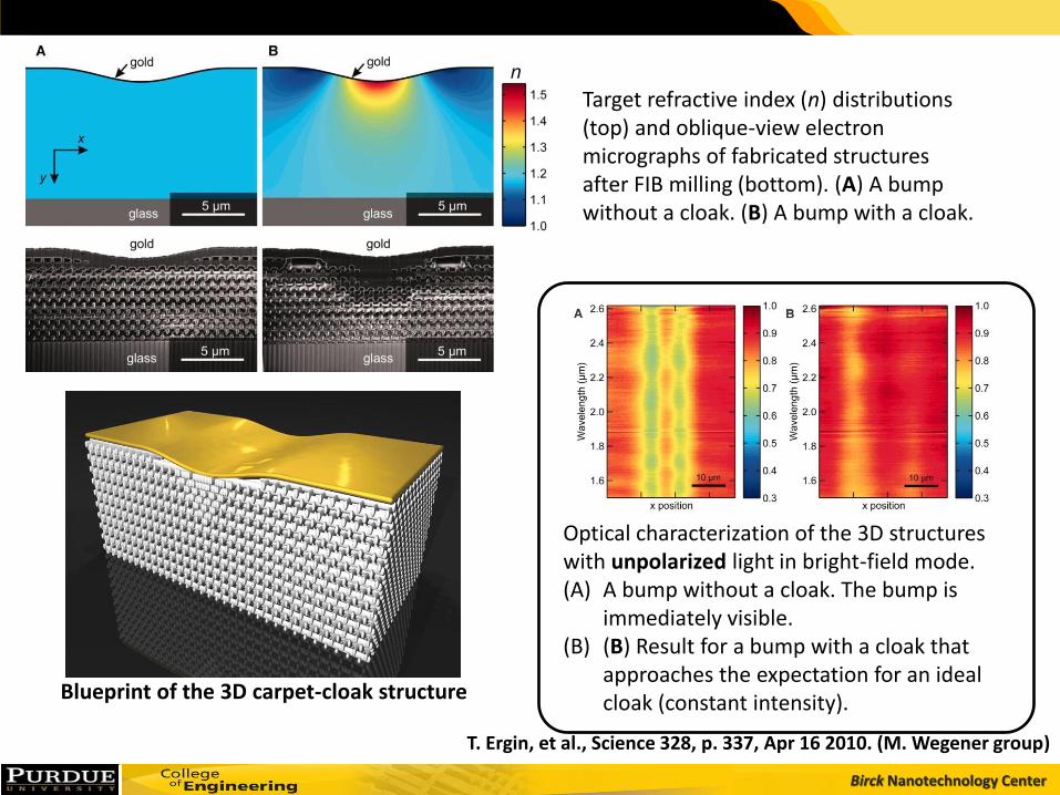
T. Ergin, et al., Science 328, p. 337, Apr 16 2010. (M. Wegener group)
Target refractive index (n) distributions (top) and oblique-view electron micrographs of fabricated structures after FIB milling (bottom). (A) A bump without a cloak. (B) A bump with a cloak.
Blueprint of the 3D carpet-cloak structure
Optical characterization of the 3D structures with unpolarized light in bright-field mode. (A) A bump without a cloak. The bump is
immediately visible. (B) (B) Result for a bump with a cloak that
approaches the expectation for an ideal cloak (constant intensity).
Birck Nanotechnology Center
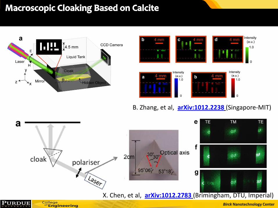
B. Zhang, et al, arXiv:1012.2238 (Singapore-MIT)
X. Chen, et al, arXiv:1012.2783 (Brimingham, DTU, Imperial)
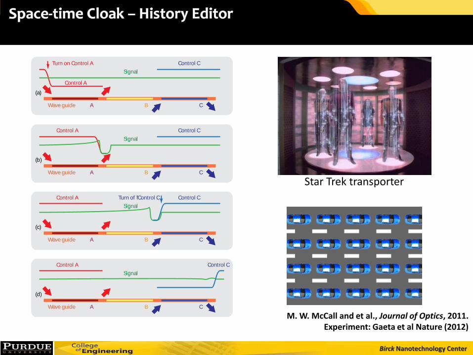
Birck Nanotechnology Center
Signal
Signal
Signal
Signal
Control C
Wave guide
Wave guide
Wave guide
Wave guide
(a)
(b)
(c)
(d)
Control C
Control C
Control C
Control A
Control A
Control A
Control A
Turn on Control A
Turn of fControl C
A B C
A B C
A B C
A B C
M. W. McCall and et al., Journal of Optics, 2011. Experiment: Gaeta et al Nature (2012)
Star Trek transporter
Birck Nanotechnology Center
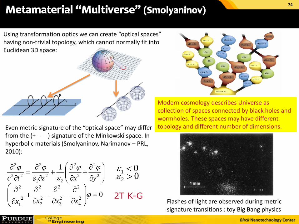
Modern cosmology describes Universe as collection of spaces connected by black holes and wormholes. These spaces may have different topology and different number of dimensions.
Using transformation optics we can create “optical spaces” having non-trivial topology, which cannot normally fit into Euclidean 3D space:
Even metric signature of the “optical space” may differ from the (+ - - - ) signature of the Minkowski space. In hyperbolic materials (Smolyaninov, Narimanov – PRL, 2010):
2
2
2
2
2
2
1
2
22
2 1
yxztc
0102
02
4
2
2
3
2
2
2
2
2
1
2
xxxx Flashes of light are observed during metric signature transitions : toy Big Bang physics
2T K-G
74
Birck Nanotechnology Center
Generalized Snell’s Law
and Negative Refraction with
Plasmonic Nanoantennas
Birck Nanotechnology Center
Birck Nanotechnology Center
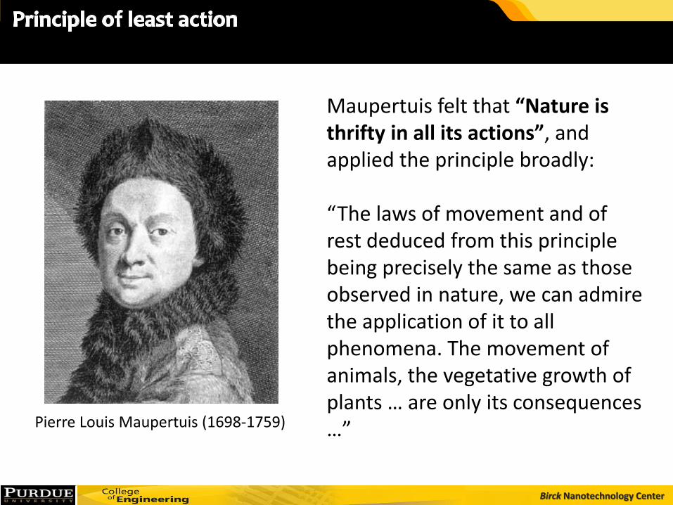
Maupertuis felt that “Nature is thrifty in all its actions”, and applied the principle broadly: “The laws of movement and of rest deduced from this principle being precisely the same as those observed in nature, we can admire the application of it to all phenomena. The movement of animals, the vegetative growth of plants … are only its consequences …” Pierre Louis Maupertuis (1698-1759)
Birck Nanotechnology Center
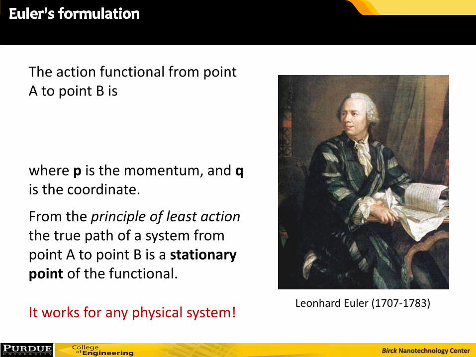
where p is the momentum, and q is the coordinate.
From the principle of least action the true path of a system from point A to point B is a stationary point of the functional.
The action functional from point A to point B is
It works for any physical system! Leonhard Euler (1707-1783)
Birck Nanotechnology Center
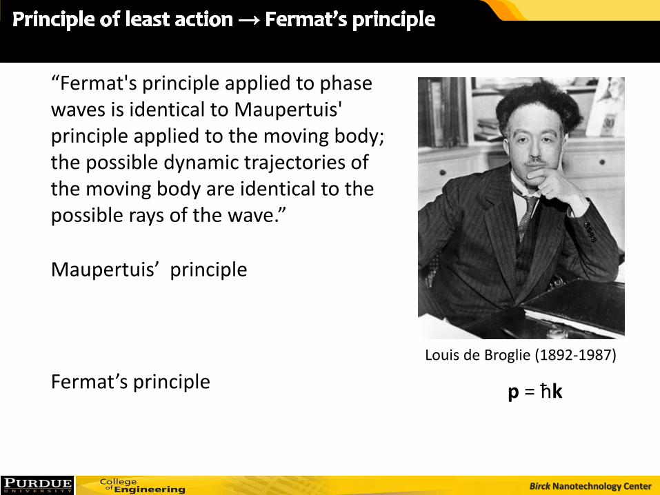
“Fermat's principle applied to phase waves is identical to Maupertuis' principle applied to the moving body; the possible dynamic trajectories of the moving body are identical to the possible rays of the wave.”
Maupertuis’ principle
Fermat’s principle
Louis de Broglie (1892-1987)
p = ħk
Birck Nanotechnology Center
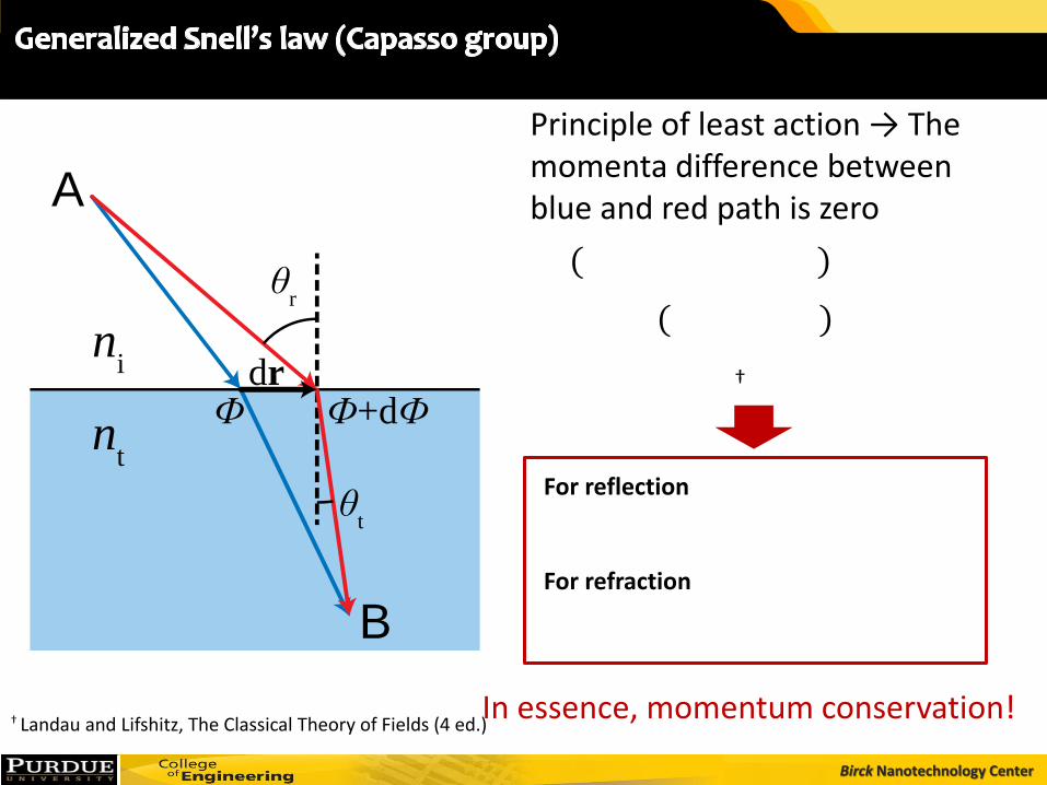
Principle of least action → The momenta difference between blue and red path is zero
For refraction
For reflection
† Landau and Lifshitz, The Classical Theory of Fields (4 ed.)
A
B
ni
Ф Ф+dФdr
θt
θr
nt
†
In essence, momentum conservation!
Birck Nanotechnology Center
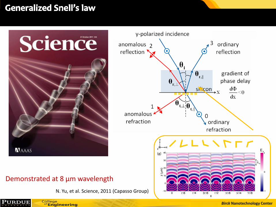
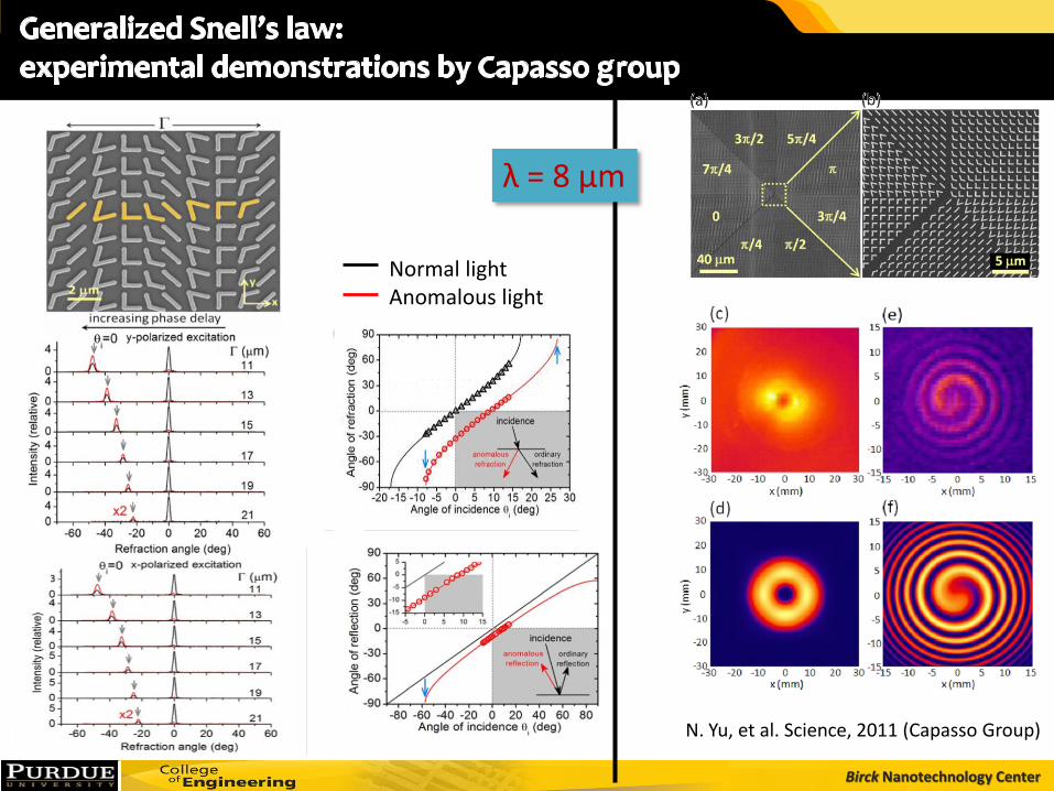
N. Yu, et al. Science, 2011 (Capasso Group)
Demonstrated at 8 µm wavelength
Birck Nanotechnology Center
Normal light Anomalous light
N. Yu, et al. Science, 2011 (Capasso Group)
λ = 8 µm
Birck Nanotechnology Center
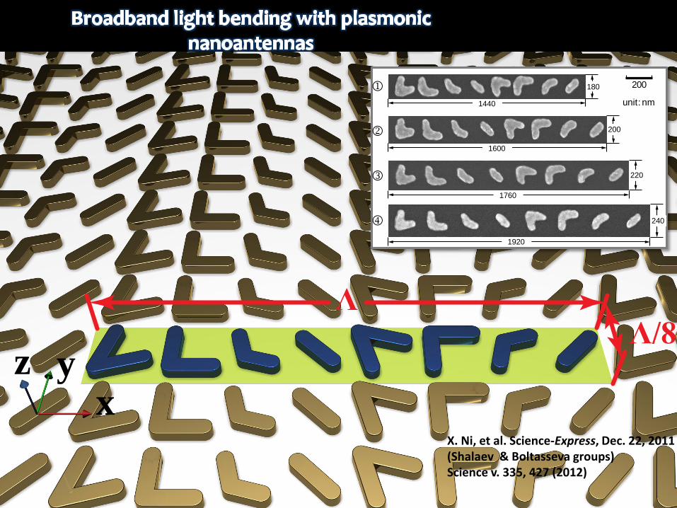
ΛΛ/8
xyz
200
1920
240
1760
220
1600
200
1440
180
unit: nm
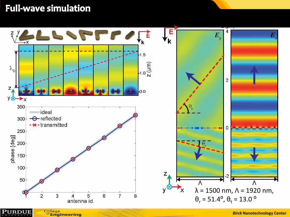
X. Ni, et al. Science-Express, Dec. 22, 2011 (Shalaev & Boltasseva groups) Science v. 335, 427 (2012)
Birck Nanotechnology Center
λ = 1500 nm, Λ = 1920 nm, θr = 51.4⁰, θt = 13.0 ⁰
Birck Nanotechnology Center
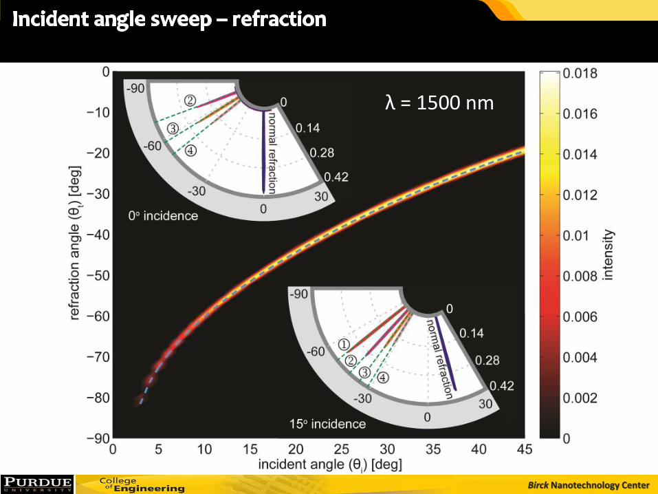
λ = 1500 nm
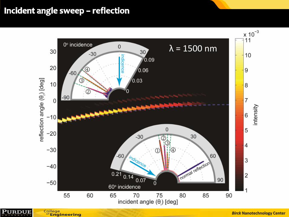
Birck Nanotechnology Center
λ = 1500 nm
Birck Nanotechnology Center
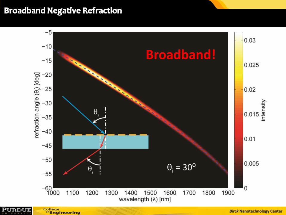
θi = 30⁰
Broadband!

Birck Nanotechnology Center
Electrical Metamaterials (Plasmonics): A Route to Nanophotonics
Optical Metamagnetics
Negative-Index Metamaterials
Active and Loss-Free Metamaterials
New Plasmonic Materials
Chiral Metamaterials
Metamaterials for Sensing
Nonlinear, Tunable, and Ultrafast Metamaterials
Quantum Optics with Metamaterials
Transformation Optics , Cloaking, and “Multiverse”
Generalized Snell’s Law and Light Bending with Nanoantennas
Birck Nanotechnology Center
88


![Mark L. Brongersma arXiv:0909.4968v2 [physics.optics] 14 Oct 2009 · 2009. 10. 14. · 17.J. P. McKelvey, “Simple iterative procedures for solving transcendental equations with](https://img.pdfslide.us/doc/110x75/606bf69e539fe12508655f69/mark-l-brongersma-arxiv09094968v2-14-oct-2009-2009-10-14-17j-p-mckelvey.jpg)


![Mark L. Brongersma arXiv:0909.4968v2 [physics.optics] 14](https://img.pdfslide.us/doc/110x75/62062ec7ce88f42f0700debb/mark-l-brongersma-arxiv09094968v2-14-.jpg)