Embed Size (px)
Citation preview
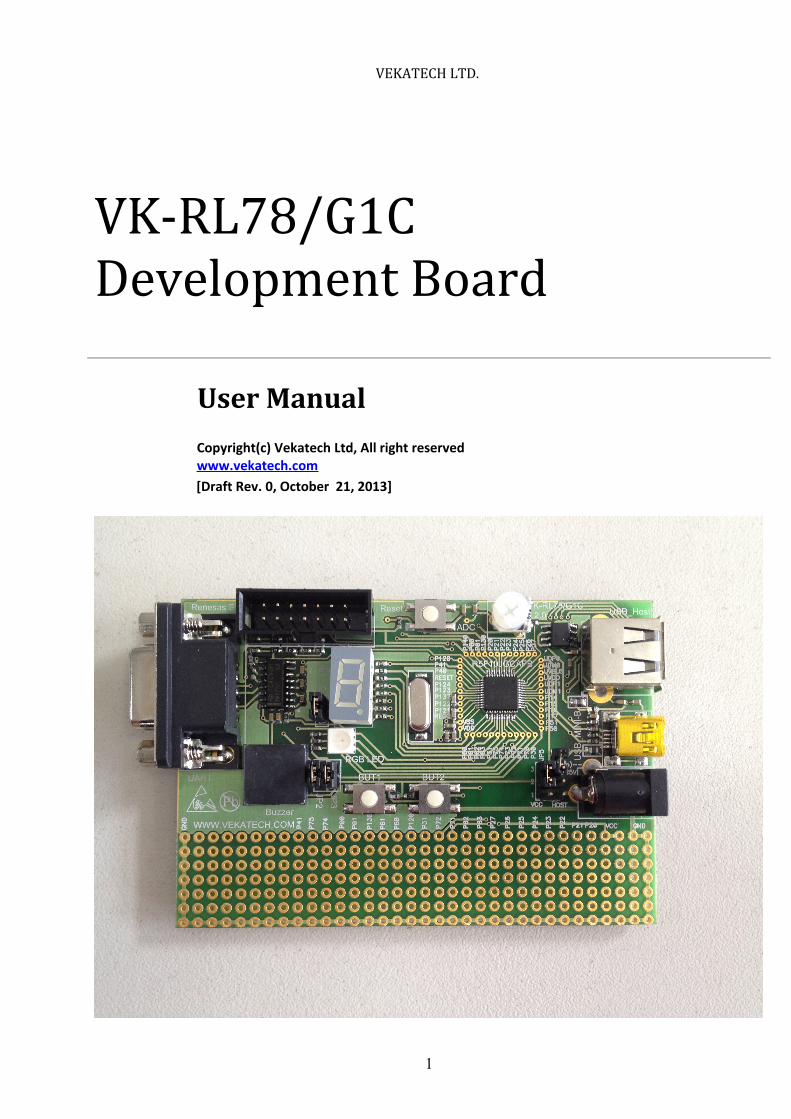
VEKATECH LTD.
VK-RL78/G1CDevelopment Board
User Manual
Copyright(c) Vekatech Ltd, All right reserved www.vekatech.com [Draft Rev. 0, October 21, 2013]
1

The document is intended to guide users with background in embedded systems to use VK-RL78/G1C Development Board in their applications.
Table of ContentsChapter 1: Introduction...............................................................................................................................3
1.1 Main features of VK-RL78/G1C......................................................................................................3
1.2 Electrostatic warning........................................................................................................................3
1.3 Processor Features............................................................................................................................3
1.4 System requirements.........................................................................................................................4
1.5 Package contents...............................................................................................................................4
1.6 Trademarks.......................................................................................................................................4
Chapter 2: VK-RL78/G1C System Configuration.....................................................................................5 2.1 Power supply circuit.........................................................................................................................5
Via DC Power Adapter:.......................................................................................................................5
Via “USB Mini-B Function Device” interface:...................................................................................5
Chapter 3: Hardware...................................................................................................................................53.1 Block Diagram..................................................................................................................................6
3.2 Hardware Components......................................................................................................................8
3.2.1 Clock Circuits:............................................................................................................................8
3.2.2 LED's:.........................................................................................................................................8
3.2.3 7 SEG LED:................................................................................................................................8
3.2.4 Piezo buzzer:...............................................................................................................................8
3.2.5 Push buttons:...............................................................................................................................8
3.2.6 ADC Potentiometer:...................................................................................................................8
3.2.7 Connectors Description:.............................................................................................................9
3.3 Jumper’s Configuration..................................................................................................................11
3.3.1 System power source................................................................................................................11
3.3.2 Host power source....................................................................................................................11
3.3.3 Power supply for BUZZER, RGB LED and 7 SEG LED........................................................12
Chapter 4: On-Chip Debugging and Flash Program................................................................................124.1 OCD via E1 Debbuger.....................................................................................................................12
Chapter 5: Software Installation...............................................................................................................12Chapter 6: Demo Project..........................................................................................................................12
6.1 Test of RP1 & 7 SEG LED..............................................................................................................13
6.2 Test of RGB LED & BUZZER.......................................................................................................13
6.3 Test of UART & USB Function.....................................................................................................14
6.4 Test of USB Host............................................................................................................................14
Chapter 7: Mechanical Dimensions...........................................................................................................15Chapter 9: Reference Designators.............................................................................................................16Chapter 10: Schematics.............................................................................................................................17Chapter 11: Troubleshooting.....................................................................................................................19Chapter 12: End.........................................................................................................................................19
2

Chapter 1: Introduction
VK-RL78/G1C is a development board, which uses MCU R5F10JGC from Renesas Electronics. This 16bit MCU supports serial interfaces such as USB HOST/FUNCTION, Serial array unit (SPI/UART/simplified I2C), I2C etc.. In addition, you will find 14 pins interface for E1 debugging, user push buttons, RGB LED, 7 Seg LED indicator, buzzer, . All this, with power supply connector connected to pin headers, unused pins of R5F10JGC, allow you to build a diversity of user applications, which could be used in a wide range of embedded tasks.
1.1 Main features of VK-RL78/G1C
MCU: RL78/G1C – R5F10JGC 1-USB HOST interface 1-USB FUNCTION interface 1-RS232 interface (MAX232) 14 pins Debug E1 connector. User 1 RGB LED and 7 segment LED. User 2 push buttons and RESET button. Power connector for External 5V Power supply. FR-4, 1.6 mm, Green/White solder mask, component print. Dimensions: 95,3mm x 65,8mm
1.2 Electrostatic warningThe VK-RL78/G1C board is shipped in protective anti-static packaging. The board must not be
subject to high electrostatic potentials. General practice for working with static sensitive devices should be applied when working with this board.
1.3 Processor FeaturesThe VK-RL78/G1C board use 16bit RL78/G1C MCU R5F10JGC from Renesas Electronics
with the following features:
ROM: 32 KB FlashData Flash: 2 KBRAM: 5632 BOperating Voltage: 2.4 V to 5.5 VMax. Frequency: 24 MHzPackage: 48 LFQFPCPU: RL78G1C coreSafety Functions: Flash CRC, RAM parity, RAM & SFR guard, Invalid memory
access, Frequency detection, A/D test, Digital output signal levelDMA: 2 channelsMain oscillator : 1 - 20 MHzLow speed internal oscillator: 15 kHz typ.High speed internal oscillator: 48/24 MHz typ. PLL: x6/x8 or 48 MHz max when using USB.I/O port: 42 (CMOS I/O: 32 + CMOS I: 5 + CMOS O: 1 + N-ch open drain I/O: 4)A/D Converter: 9 channels
3
Timers :
Timer Array Unit: 16-bit x 1 unit x 4 channels Window watchdog timer: 1 channel Real-time clock: 1 channel Interval timer: 12-bit 1 unit x 1 channel
Serial Interface :
SERIAL ARRAY UNIT:
CSI x 2 channels / UART x 1 channel / Simplified I2C x 2 channel
I2C: 1 channel
Interrupt:
Maskable: External 10
Power on ResetVoltage DetectorKey interrupt: 6 channelsClock output / Buzzer outputBCD correctionOn-chip debugg functionOperating temperature:-40 to +85 °C
For more information, please visit www.renesas.eu
1.4 System requirementsHost PC: A PC for CubeSuite+ V2.0.00.00 demo-version supportingWindows 2000, Windows XP, Windows Vista or Widows 7.Adobe Acrobat Reader.
1.5 Package contentsVK-RL78/G1C board.3M glue legs.CD with demo projects.
1.6 TrademarksCopyright © 2013 Vekatech Ltd. Copyrighted materials not owned by Vekatech & Associates
are the property of their respective owners. All other trademarks and service marks contained on this article are the trademarks of their respective owners.
4
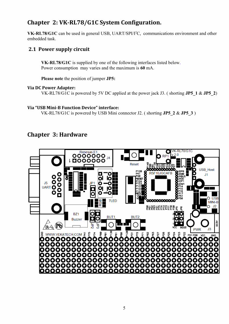
Chapter 2: VK-RL78/G1C System Configuration.
VK-RL78/G1C can be used in general USB, UART/SPI/I2C, communications environment and other embedded task.
2.1 Power supply circuit
VK-RL78/G1C is supplied by one of the following interfaces listed below. Power consumption may varies and the maximum is 60 mA.
Please note the position of jumper JP5:
Via DC Power Adapter:VK-RL78/G1C is powered by 5V DC applied at the power jack J3. ( shorting JP5_1 & JP5_2)
Via “USB Mini-B Function Device” interface:VK-RL78/G1C is powered by USB Mini connector J2. ( shorting JP5_2 & JP5_3 )
Chapter 3: Hardware
5
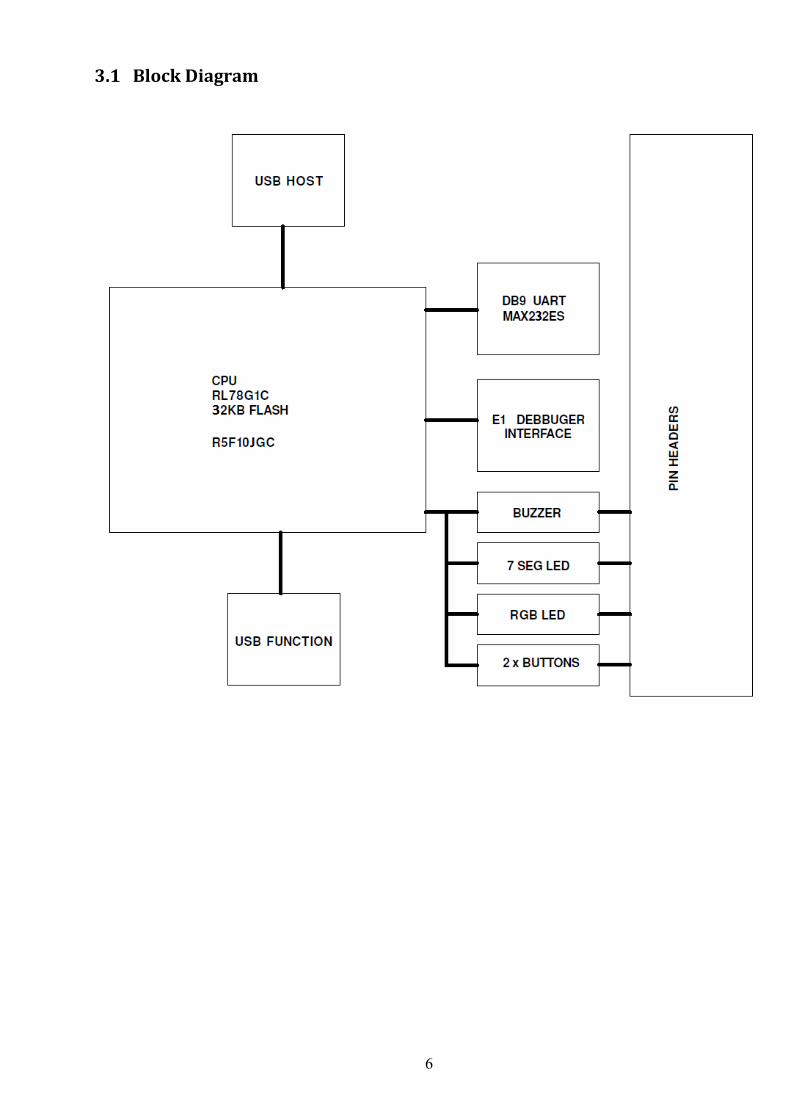
3.1 Block Diagram
6

3.2 Hardware Components
3.2.1 Clock Circuits:Quartz crystal 8.000 MHz is connected to R5F10JGC (X1) 45 pin and (X2) 44 pin.
3.2.2 LED's:RGB LED
Component Signal name Pin name MCU pinD4 Red R_PWM P3_1 5 pin (R5F10JGC)D4 Green G_PWM P7_2 9 pin (R5F10JGC)D4 Blue B_PWM P7_1 10 pin (R5F10JGC)
3.2.3 7 SEG LED:Kingbright SA36-11SRWA
Signal Name Pin name Pin #SEG_A P4_1 38SEG_B P6_0 1SEG_C P7_5 6SEG_D P13_0 33SEG_E P0_1 34SEG_F P6_1 2SEG_G P7_4 7
SEG_DP P0_0 35
3.2.4 Piezo buzzer:Murrata PKLCS 1212E4001-R1
Component Signal name Pin name MCU pin BZ1 BUZZER P140 36
3.2.5 Push buttons:Component Signal name Pin name MCU pinSW1 T_RESET_N RESET 40SW2 BUT1 P62 3SW3 BUT2 P63 4
3.2.6 ADC Potentiometer:Component Signal name Pin name MCU pinRP1 ADC_POT P120 37
7
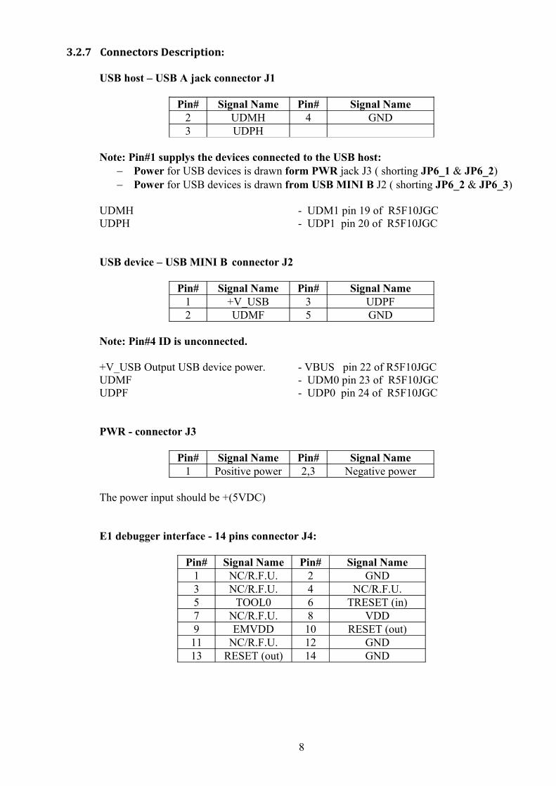
3.2.7 Connectors Description:
USB host – USB A jack connector J1
Pin# Signal Name Pin# Signal Name2 UDMH 4 GND3 UDPH
Note: Pin#1 supplys the devices connected to the USB host: Power for USB devices is drawn form PWR jack J3 ( shorting JP6_1 & JP6_2) Power for USB devices is drawn from USB MINI B J2 ( shorting JP6_2 & JP6_3)
UDMH - UDM1 pin 19 of R5F10JGCUDPH - UDP1 pin 20 of R5F10JGC
USB device – USB MINI B connector J2
Pin# Signal Name Pin# Signal Name1 +V_USB 3 UDPF2 UDMF 5 GND
Note: Pin#4 ID is unconnected.
+V_USB Output USB device power. - VBUS pin 22 of R5F10JGCUDMF - UDM0 pin 23 of R5F10JGCUDPF - UDP0 pin 24 of R5F10JGC
PWR - connector J3
Pin# Signal Name Pin# Signal Name1 Positive power 2,3 Negative power
The power input should be +(5VDC)
E1 debugger interface - 14 pins connector J4:
Pin# Signal Name Pin# Signal Name1 NC/R.F.U. 2 GND3 NC/R.F.U. 4 NC/R.F.U.5 TOOL0 6 TRESET (in)7 NC/R.F.U. 8 VDD9 EMVDD 10 RESET (out)11 NC/R.F.U. 12 GND13 RESET (out) 14 GND
8
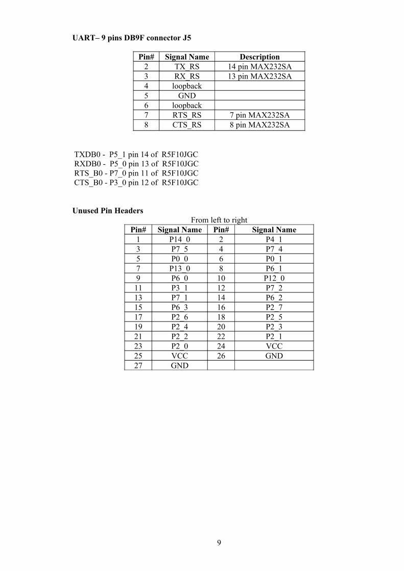
UART– 9 pins DB9F connector J5
Pin# Signal Name Description2 TX_RS 14 pin MAX232SA3 RX_RS 13 pin MAX232SA4 loopback5 GND6 loopback7 RTS_RS 7 pin MAX232SA8 CTS_RS 8 pin MAX232SA
TXDB0 - P5_1 pin 14 of R5F10JGCRXDB0 - P5_0 pin 13 of R5F10JGCRTS_B0 - P7_0 pin 11 of R5F10JGCCTS_B0 - P3_0 pin 12 of R5F10JGC
Unused Pin Headers From left to right
Pin# Signal Name Pin# Signal Name1 P14_0 2 P4_13 P7_5 4 P7_45 P0_0 6 P0_17 P13_0 8 P6_19 P6_0 10 P12_011 P3_1 12 P7_213 P7_1 14 P6_215 P6_3 16 P2_717 P2_6 18 P2_519 P2_4 20 P2_321 P2_2 22 P2_123 P2_0 24 VCC25 VCC 26 GND27 GND
9
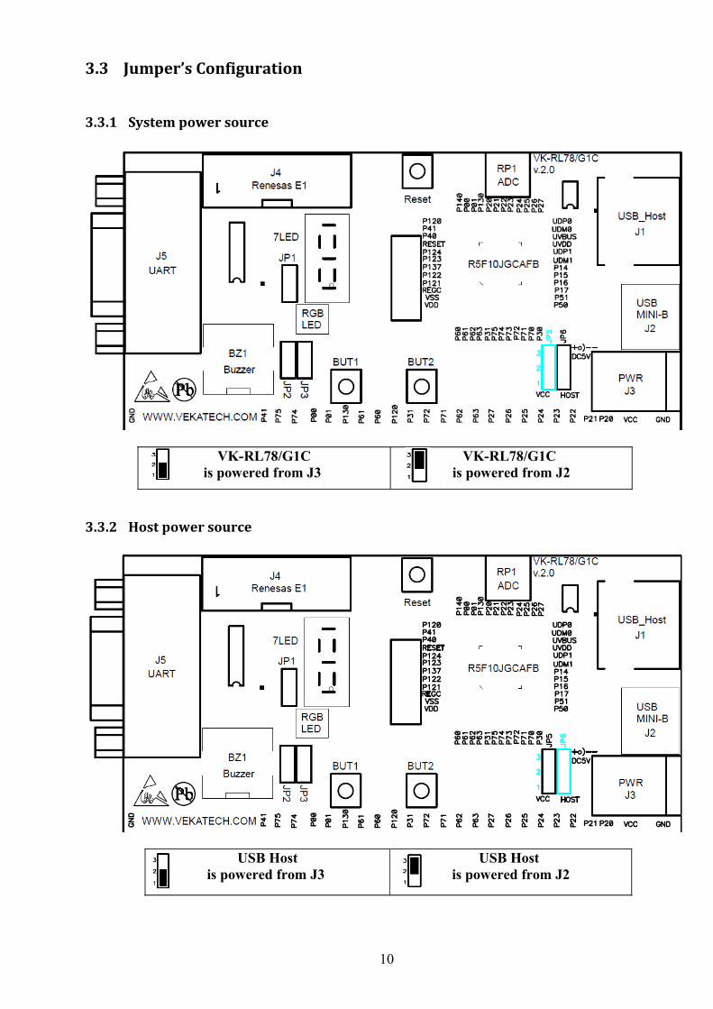
3.3 Jumper’s Configuration
3.3.1 System power source
VK-RL78/G1Cis powered from J3
VK-RL78/G1C is powered from J2
3.3.2 Host power source
USB Hostis powered from J3
USB Host is powered from J2
10

3.3.3 Power supply for BUZZER, RGB LED and 7 SEG LED
JP1 powers the7 SEG LED
JP2 powers theBUZZER
JP3 powers theRGB LED
Chapter 4: On-Chip Debugging and Flash Program
4.1 OCD via E1 DebbugerE1 Debugger can be connected to J4 to debug user applications. Renesas Electronics Flash
Programmer 2.00 can be used as Flash programming tool.
Chapter 5: Software Installation
This manual is not intended to guide you through installation procedures of any development or application software. Please refer to the relevant sources.
Chapter 6: Demo Project
It contains sample application which tests the periphery of the kit VK- RL78\G1CThe test includes: RP1, 7 SEG LED, RGB LED, BUZZER, UART, USB FUNCTION, USB HOST, BUT1, BUT2.
The available project is prepared to compile with Cubesuit+ tool chain.
The project is located in CD \ sw_kit \ RENESAS \
11
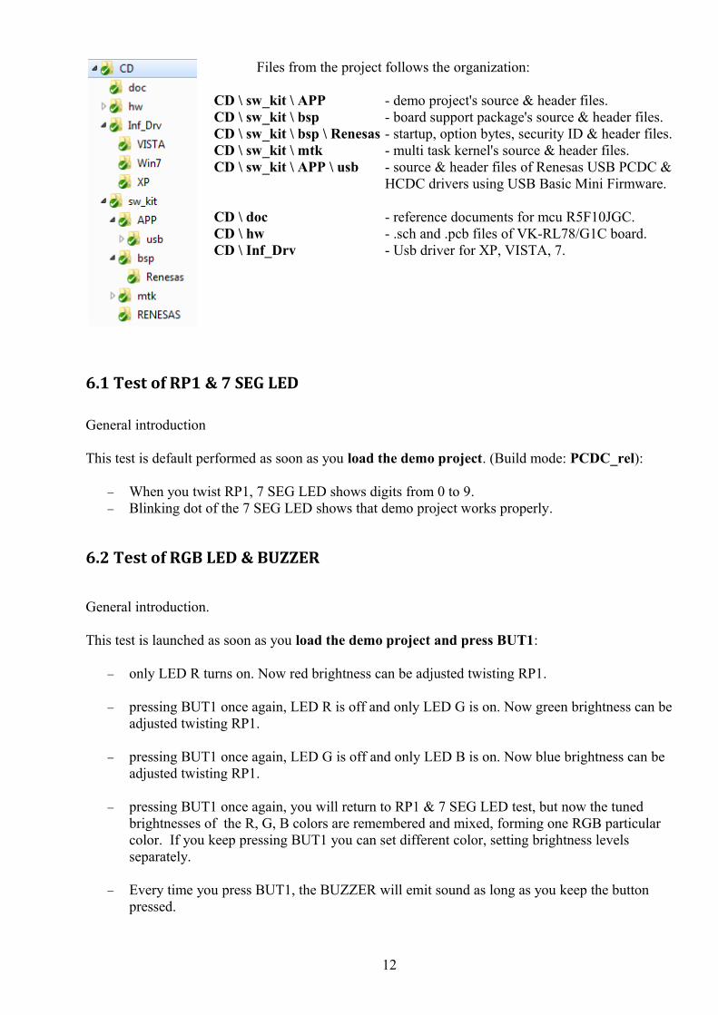
Files from the project follows the organization:
CD \ sw_kit \ APP - demo project's source & header files.CD \ sw_kit \ bsp - board support package's source & header files.CD \ sw_kit \ bsp \ Renesas - startup, option bytes, security ID & header files.CD \ sw_kit \ mtk - multi task kernel's source & header files.CD \ sw_kit \ APP \ usb - source & header files of Renesas USB PCDC &
HCDC drivers using USB Basic Mini Firmware.
CD \ doc - reference documents for mcu R5F10JGC.CD \ hw - .sch and .pcb files of VK-RL78/G1C board.CD \ Inf_Drv - Usb driver for XP, VISTA, 7.
6.1 Test of RP1 & 7 SEG LED
General introduction
This test is default performed as soon as you load the demo project. (Build mode: PCDC_rel):
When you twist RP1, 7 SEG LED shows digits from 0 to 9. Blinking dot of the 7 SEG LED shows that demo project works properly.
6.2 Test of RGB LED & BUZZER
General introduction.
This test is launched as soon as you load the demo project and press BUT1:
only LED R turns on. Now red brightness can be adjusted twisting RP1.
pressing BUT1 once again, LED R is off and only LED G is on. Now green brightness can be adjusted twisting RP1.
pressing BUT1 once again, LED G is off and only LED B is on. Now blue brightness can be adjusted twisting RP1.
pressing BUT1 once again, you will return to RP1 & 7 SEG LED test, but now the tuned brightnesses of the R, G, B colors are remembered and mixed, forming one RGB particular color. If you keep pressing BUT1 you can set different color, setting brightness levels separately.
Every time you press BUT1, the BUZZER will emit sound as long as you keep the button pressed.
12
6.3 Test of UART & USB Function
General introduction.
This test is launched as soon as you load the demo project. This test needs a PC application such as (Terminal, PUTTY, Hyper terminal, ets.) and mini usb cable. PC recognizes VK-RL78/G1C as virtual COM port. To perform the test please connect pin2 and pin3 of the DB9F connector (to build loop back connection).
USB <=> UART: performs echo on virtual COM port. When this port is open with default configuration (9600 bps, 8 bit data, No parity, 1 stop) comport application should read the same data that was sent. If everyting's right (see the same as what you are typing) it means that USB Function and UART works properly.
6.4 Test of USB Host
General introduction.
This test is launched as soon as you load the demo project. (Build mode: HCDC_rel):This test needs another VK-RL78/G1C board (programmed with Build mode: PCDC_rel) or any other USB <=> UART converter ( using Abstract Control Model Serial Emulation Device CDC Class ), a PC application (such as Terminal, PUTTY, Hyper terminal, ets.), a serial cable and com port.
USB Host: performs echo of the incoming characters from VK-RL78/G1C usb function board USB <=> UART converter. Default configuration after reset is 9600 bps, 8 bit data, No parity, 1 stop.
pressing BUT1, the 7 SEG LED shows 'b'. which means baud rate can be changed. Pressing BUT2 frequently, the 7 SEG LED shows '0', '1', '2', '3', '4', '5', '6', '7', '0', … which means 1200bps, 2400bps, 4800bps, 9600bps, 14400bps, 19200bps, 38400bps, 57600bps, 1200bps ...is selected. Pressing BUT1 applies the selected baud rate and turns the LED R on. Now red brightness can be adjusted twisting RP1.
pressing BUT1 frequently, the behavior is the same as Build mode: PCDC_rel. You can read theposition of the RP1, set the brightnesses of R, G, B colors separately or change the baud rate. Every press of BUT1 will make the BUZZER to emit sound. The sound will last as long as BUT1 is kept pressed.
13
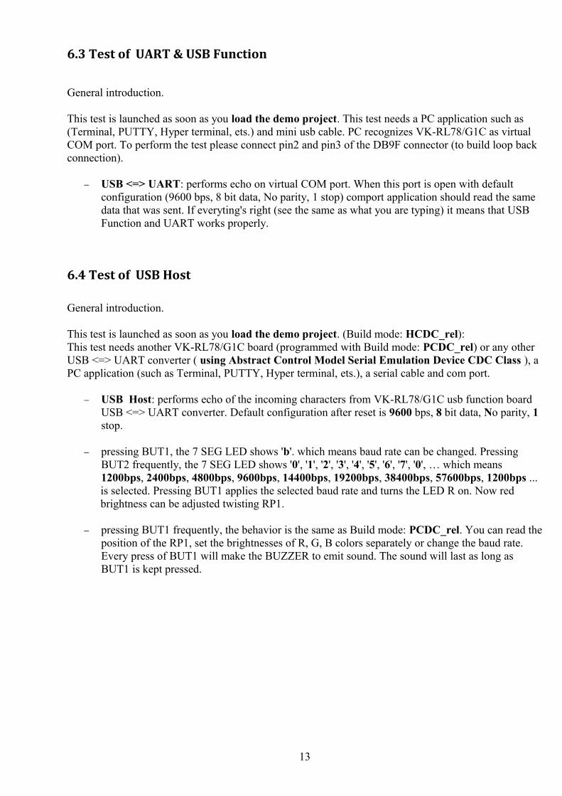
Chapter 7: Mechanical Dimensions
All measures are in mm.
14
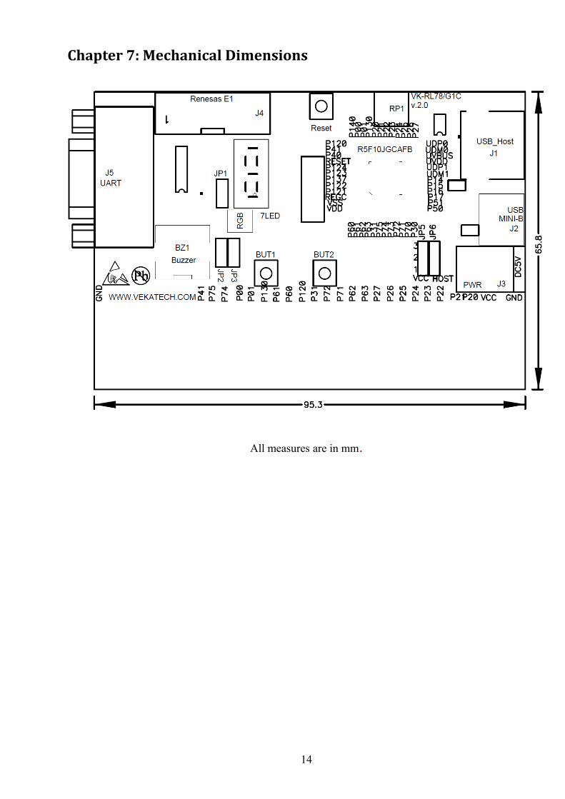
Chapter 9: Reference Designators
15

Chapter 10: Schematics
16
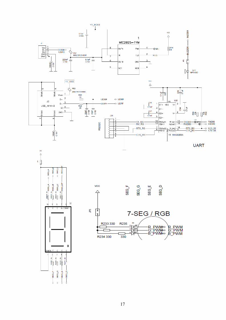
17
Chapter 11: Troubleshooting
Chapter 12: End
18