Embed Size (px)
Citation preview

1
VIVEKANANDHA COLLEGE OF ENGINEERING FOR
WOMEN (Autonomous Institution, Affiliated to Anna University, Chennai)
Elayampalayam, Tiruchengode – 637 205
M.E. VLSI DESIGN
Regulation 2015
CHOICE BASED CREDIT SYSTEM
PROGRAMME EDUCATIONAL OBJECTIVES (PEOS)
PEO I. To acquire a background in Basic science and Mathematics and ability to
use these tools in VLSI Design.
PEO II. Teach students to understand the principles involved in the latest software
required for designing and critically analyzing electronic systems relevant
to industry and society.
PEO III. To attain the qualities of professional leadership to deliver effectively in a
multi-disciplinary team and domains
PEO IV. Mould students to be able to communicate efficiently
PEO V. Motivate students to take up socially relevant and challenging projects and
propose innovative solution to problems for the benefit of society.

2
PROGRAMME OUTCOMES (POS)
PO 1. Apply knowledge of Mathematics, Science, Engineering fundamentals and an
Engineering specialization to the conceptualization of Engineering models.
PO 2. Identify, formulate, research literature and solve complex Electronics and
communication Engineering problems reaching substantiated conclusions
using first principles of Mathematics and Engineering sciences.
PO 3. Design solutions for complex Electronics and Communication Engineering
problems and design systems, components or processes that meet specified
needs with appropriate consideration for public health and safety, cultural,
societal, and environmental considerations.
PO 4. Conduct investigations of complex problems including design of experiments,
analysis and interpretation of data, and synthesis of information to provide
valid conclusions.
PO 5. Create, select and apply appropriate techniques, resources, and modern
Engineering tools, including prediction and modeling, to complex Electronics
and Communication Engineering activities, with an understanding of the
limitations.
PO 6. Function effectively as an individual, and as a member or leader in diverse
teams and in multi - disciplinary settings.
PO 7. Communicate effectively on complex Electronics and Communication
Engineering activities with the Engineering community and with society at
large, such as being able to comprehend and write effective reports and design
documentation, make effective presentations, and give and receive clear
instructions.
PO 8. Demonstrate understanding of the societal, health, safety, legal and cultural
issues and the consequent responsibilities relevant to Engineering practice.
PO 9. Understand and commit to professional ethics and responsibilities and norms
of Engineering practice.
PO 10. Understand the impact of Engineering solutions in a societal context and
demonstrate knowledge of and need for sustainable development.
PO 11. Demonstrate a knowledge and understanding of management and business
practices, such as risk and change management, and understand their
limitations.
PO 12. Recognize the need for, and have the ability to engage in independent and
lifelong learning.

3
MAPPING OF PROGRAMME EDUCATIONAL OBJECTIVES (PEOS) WITH
PROGRAMME OUTCOMES (POS)
A broad relation between the programme objective and the outcomes is given in the
following table
PROGRAMME
EDUCATIONAL
OBJECTIVES
PROGRAMME OUTCOMES
PO 1 PO 2 PO 3 PO 4 PO 5 PO 6 PO 7 PO 8 PO 9 PO 10 PO 11 PO 12
PEO 1
PEO 2
PEO 3
PEO 4
PEO 5

4
SEM Course PO1 PO2 PO3 PO4 PO5 PO6 PO7 PO8 PO 9 PO10 PO11 PO12
I
Applied
Mathematics
Advanced
Digital System
Design
Solid State
Devices
VLSI
Technology
CMOS Analog
VLSI Design
Professional
Elective – I
VLSI
Laboratory - I
II
Low Power
VLSI Design
Testing and
Verification of
VLSI Circuits
Research
Methodology
and Data
analysis
Professional
Elective – II
Professional
Elective – III
Open Elective -
I
VLSI
Laboratory - II
Technical
Seminar
III
Professional
Elective – IV
Professional
Elective - V
Open Elective
- II
Project Phase -
I
IV Project Phase -
II

5
VIVEKANANDHA COLLEGE OF ENGINEERING FOR WOMEN
(Autonomous Institution Affiliated to Anna University Chennai)
Elayampalayam, Tiruchengode – 637 205
Programme M.E. Programme Code 205 Regulation 2015
Department VLSI DESIGN / ELECTRONICS AND
COMMUNICATION ENGINEERING Semester I
CURRICULUM
(Applicable to the students admitted from the academic year 2015-2016 onwards)
Course Code Course Name Category Periods / Week Credit Maximum Marks
L T P C CA ESE Total
THEORY
P15MA102 Applied Mathematics FC 3 0 0 3 50 50 100
P15VD101 Advanced Digital System
Design PC 3 0 0 3 50 50 100
P15VD102 Solid State Devices PC 3 0 0 3 50 50 100
P15VD103 VLSI Technology PC 3 0 0 3 50 50 100
P15VD104 CMOS Analog VLSI Design PC 3 0 0 3 50 50 100
Professional Elective – I PE 3 0 0 3 50 50 100
PRACTICAL
P15VD105 VLSI Laboratory - I PC 0 0 4 2 50 50 100
Total Credits 20 350 350 700
CA - Continuous Assessment, ESE - End Semester Examination, PC – Professional Core, PE –
Professional Elective, FC – Foundation Course

6
VIVEKANANDHA COLLEGE OF ENGINEERING FOR WOMEN
(Autonomous Institution Affiliated to Anna University Chennai)
Elayampalayam, Tiruchengode – 637 205
Programme M.E. Programme Code 205 Regulation 2015
Department VLSI DESIGN / ELECTRONICS AND
COMMUNICATION ENGINEERING Semester II
CURRICULUM
(Applicable to the students admitted from the academic year 2015-2016 onwards)
Course Code Course Name Category Periods / Week Credit Maximum Marks
L T P C CA ESE Total
THEORY
P15VD206 Low Power VLSI Design PC 3 0 0 3 50 50 100
P15VD207 Testing and Verification of
VLSI Circuits PC 3 0 0 3 50 50 100
P15VD208 Research Methodology and
Data analysis EEC 3 0 0 3 50 50 100
Open Elective - I OE 3 0 0 3 50 50 100
Professional Elective – II PE 3 0 0 3 50 50 100
Professional Elective – III PE 3 0 0 3 50 50 100
PRACTICAL
P15VD209 VLSI Laboratory – II PC 0 0 4 2 50 50 100
P15VD210 Technical Seminar EEC 0 0 2 1 100 -- 100
Total Credits 21 450 350 800
PC – Professional Course, PE – Professional Elective, OE – Open Elective, EEC – Enhanced
Employability Course, CA - Continuous Assessment, ESE - End Semester Examination
*Common syllabus for M.E.-.AE, M.E.- CSE, M.E.- PSE & M.Tech.- IT

7
VIVEKANANDHA COLLEGE OF ENGINEERING FOR WOMEN
(Autonomous Institution Affiliated to Anna University Chennai)
Elayampalayam, Tiruchengode – 637 205
Programme M.E. Programme Code 205 Regulation 2015
Department VLSI DESIGN / ELECTRONICS AND
COMMUNICATION ENGINEERING Semester III
CURRICULUM
(Applicable to the students admitted from the academic year 2015-2016 onwards)
Course Code Course Name Category Periods / Week Credit Maximum Marks
L T P C CA ESE Total
THEORY
Open Elective - II PE 3 0 0 3 50 50 100
Professional Elective – IV PE 3 0 0 3 50 50 100
Professional Elective - V OE 3 0 0 3 50 50 100
PRACTICAL
P15VD311 Project Phase - I EEC 0 0 12 6 60 40 100
Total Credits 15 210 190 400
PE – Professional Elective, OE – Open Elective, EEC – Enhanced Employability Course,
CA - Continuous Assessment, ESE - End Semester Examination

8
VIVEKANANDHA COLLEGE OF ENGINEERING FOR WOMEN
(Autonomous Institution Affiliated to Anna University Chennai)
Elayampalayam, Tiruchengode – 637 205
Programme M.E. Programme Code 205 Regulation 2015
Department VLSI DESIGN / ELECTRONICS AND
COMMUNICATION ENGINEERING Semester IV
CURRICULUM
(Applicable to the students admitted from the academic year 2015-2016 onwards)
Course Code Course Name Category Periods / Week Credit Maximum Marks
L T P C CA ESE Total
PRACTICAL
P15VD412 Project Phase – II EEC 0 0 24 12 60 40 100
Total Credits 12 60 40 100
EEC – Enhanced Employability Course, CA - Continuous Assessment, ESE - End Semester
Examination
Cumulative Course Credits - 68

9
PROFESSIONAL CORE (PC)
Course
Code Course Name Category
Periods / Week Credit Maximum Marks
L T P C CA ESE Total
P15VD101 Advanced Digital
System Design PC 3 0 0 3 50 50 100
P15VD102 Solid State Devices PC 3 0 0 3 50 50 100
P15VD103 VLSI Technology PC 3 0 0 3 50 50 100
P15VD104 CMOS Analog VLSI
Design PC 3 0 0 3 50 50 100
P15VD105 VLSI Laboratory - I PC 0 0 4 2 50 50 100
P15VD206 Low Power VLSI
Design
PC
3 0 0 3 50 50 100
P15VD207 Testing and Verification
of VLSI Circuits PC 3 0 0 3 50 50 100
P15VD209 VLSI Laboratory – II PC 0 0 4 2 50 50 100
ENHANCED EMPLOYABILITY COURSES (EEC)
Course
Code Course Name Category
Periods / Week Credit Maximum Marks
L T P C CA ESE Total
Research
Methodology and
Data analysis
EEC 3 0 0 3 50 50 100
Technical Seminar EEC 0 0 2 1 100 - 100
Project Phase – II EEC 0 0 24 12 50 50 100
FOUNDATION COURSE (FC)
Course
Code Course Name Category
Periods / Week Credit Maximum Marks
L T P C CA ESE Total
P15MA102 Applied
Mathematics FC 3 0 0 3 50 50 100

10
PROFESSIONAL ELECTIVE (PE)
Course Code Course Name Periods / Week Credit Maximum Marks
L T P C CA ESE Total
P15VDE01 Simulation of Circuits and Devices 3 0 0 3 50 50 100
P15VDE02 Hardware Design Verification Techniques 3 0 0 3 50 50 100
P15VDE03 Advanced Digital Signal Processing 3 0 0 3 50 50 100
P15VDE04 RF Microelectronics Chip Design 3 0 0 3 50 50 100
P15VDE05 Physics of MOS Transistors 3 0 0 3 50 50 100
P15VDE06 VLSI Design 3 0 0 3 50 50 100
P15VDE07 Foundations of VLSI CAD 3 0 0 3 50 50 100
P15VDE08 Wavelets and Sub Band Coding 3 0 0 3 50 50 100
P15VDE09 Embedded System Design 3 0 0 3 50 50 100
P15VDE10 VLSI Signal Processing 3 0 0 3 50 50 100
P15VDE11 Mixed Signal VLSI Design 3 0 0 3 50 50 100
P15VDE12 Hardware Description Language 3 0 0 3 50 50 100
P15VDE13 Processors and Embedded Controllers 3 0 0 3 50 50 100
P15VDE14 Multimedia Compression Techniques 3 0 0 3 50 50 100
P15VDE15 Analog VLSI Design 3 0 0 3 50 50 100
P15VDE16 Introduction to MEMS 3 0 0 3 50 50 100
P15VDE17 Reconfigurable Architectures and
Computing 3 0 0 3 50 50 100
P15VDE18 Semiconductor Memory Design 3 0 0 3 50 50 100
P15VDE19 System Design using FPGA 3 0 0 3 50 50 100
P15VDE20 System on Chip Design 3 0 0 3 50 50 100
P15VDE21 Nano Electronics 3 0 0 3 50 50 100
P15VDE22 Communication Networks 3 0 0 3 50 50 100
P15VDE23 VLSI for Wireless Communication 3 0 0 3 50 50 100
P15VDE24 Three Dimensional Networks on Chip 3 0 0 3 50 50 100
P15VDE25 ARM Processors and Applications 3 0 0 3 50 50 100
P15VDE26 ASIC Design 3 0 0 3 50 50 100
CA - Continuous Assessment, ESE - End Semester Examination

11
VIVEKANANDHA COLLEGE OF ENGINEERING FOR WOMEN
(Autonomous Institution Affiliated to Anna University Chennai)
Elayampalayam, Tiruchengode – 637 205
Programme M.E. Programme Code 205 Regulation 2015
Department VLSI DESIGN / ELECTRONICS AND
COMMUNICATION ENGINEERING Semester I
Course
Code Course Name
Periods / Week Credit Maximum Marks
L T P C CA ESE Total
P15MA102 Applied Mathematics 3 0 0 3 50 50 100
Course
Objective
To expose fundamental knowledge in 1D Random Variables and testing the
hypothesis.
To analyze linear programming, Computational methods in Engineering and various
queuing models.
Unit – I ONE DIMENSIONAL RANDOM VARIABLE Periods 9
Random Variables- Probability Function-Moments-Moment Generating Function & their Properties-
Binomial, Poisson, Geometric, Uniform, Exponential Distributions.
Unit – II TESTING OF HYPOTHESIS Periods 9
Basic Definitions:- ( Population, Sampling, Tests of Significance, Testing a Hypothesis, Null Hypothesis,
Alternative Hypothesis, Level of Significance, Types of Errors ) – Testing of Hypothesis using : „t‟-Test , „F‟-
Test , Chi Square Test ( ψ2) - Test for Independence of Attributes & Goodness of Fit.
Unit – III LINEAR PROGRAMMING Periods 9
Formulation-Graphical solution-Simplex Method -Transportation and Assignment problems.
Unit – IV DYNAMIC PROGRAMMING Periods 9
Dynamic Programming-principle of optimality-forward and backward recursion-DP Applications (Cargo
loading method)-Problems of dimensionality.
Unit – V QUEUING MODELS Periods 9
Introduction-Markovian Models: M/M/1: infinite capacity-M/M/C: infinite capacity-M/M/1: finite capacity –
M/M/C: finite capacity, Little‟s formula.
Total Periods 45
REFERENCES:
1. B. V. Ramana,“Higher Engineering Mathematics”, Tata Mc Graw Hill Publishing Pvt Ltd, New Delhi,
2008.
2. Taha,H.a. “Operations Research: An Introduction”, 7
th Edition, Person Education , Asia, New Delhi,
2002.
3. Moon, T. K., Sterling, W. C., “Mathematical Methods and Algorithms for Signal Processing”, Pearson
Education, 2000.
4. Donald Gross and Carl M. Harris, “Fundamentals of Queuing Theory”, 2
nd Edition, John Wiley and
Sons, New York, 1985.
5. Richard Johnson, Miller & Freund‟s “Probability and Statistics for Engineers”, 7
th Edition, Prentice-
Hall of India, Private Ltd., New Delhi, 2007.
Course
Outcome
Can expose fundamental knowledge in 1D Random Variables and testing the
hypothesis.
Able to analyze linear programming, Computational methods in Engineering and
various queuing models.

12
VIVEKANANDHA COLLEGE OF ENGINEERING FOR WOMEN
(Autonomous Institution Affiliated to Anna University Chennai)
Elayampalayam, Tiruchengode – 637 205
Programme M.E. Programme Code 205 Regulation 2015
Department VLSI DESIGN /ELECTRONICS AND
COMMUNICATION ENGINEERING Semester I
Course Code Course Name
Periods / Week Credit Maximum Marks
L T P C CA ESE Total
P15VD101 Advanced Digital System Design 3 0 0 3 50 50 100
Course
Objective
To provide an in-depth knowledge of synchronous and asynchronous sequential
circuits analysis and design.
To provide the basics of fault diagnosis and testing algorithms.
To study the design of synchronous sequential circuits using PLDs.
To study the design of digital systems using VHDL.
Unit - I SEQUENTIAL CIRCUIT DESIGN Periods 9
Analysis of clocked synchronous sequential circuits and modeling- State diagram, state table, state
assignment and state reduction-Design of synchronous sequential circuits -Design of iterative circuits-ASM
chart and realization using ASM.
Unit - II ASYNCHRONOUS SEQUENTIAL CIRCUIT DESIGN Periods 9
Analysis of asynchronous sequential circuit – flow table reduction-races-state assignment-transition table and
problems in transition table- design of asynchronous sequential circuit-Static, dynamic and essential hazards –
data synchronizers – Mixed operating mode asynchronous circuits.
Unit - III FAULT DIAGNOSIS AND TESTABILITY
ALGORITHMS Periods 9
Fault table method-path sensitization method – Boolean difference method-D algorithm - Tolerance
techniques – The compact algorithm – Fault in PLA – Test generation-DFT schemes – Built in self test.
Unit - IV SYNCHRONOUS DESIGN USING PROGRAMMABLE
DEVICES Periods 9
Programming logic device families – Designing a synchronous sequential circuit using PLA/PAL –
Realization of finite state machine using PLD – FPGA – Xilinx FPGA-Xilinx 4000.
Unit - V SYSTEM DESIGN USING VHDL Periods 9
VHDL operators – Arrays – concurrent and sequential statements – packages- Data flow – Behavioral –
structural modeling – compilation and simulation of VHDL code –Test bench - Realization of combinational
and sequential circuits using HDL – Registers – counters – sequential machine – serial adder – Multiplier-
Divider – Design of simple microprocessor.
Total Periods 45
REFERENCES:
1. Donald D.Givone, “Digital Principles and Design”, Tata McGraw-Hall, 19th 2011.
2. Nripendra N Biswas ,“Logic Design Theory” ,Prentice Hall of India, 2001
3. Charles H Roth, Jr. “Fundamentals of Logic Design” ,Thomson Learning, 2004
4. Douglas L.Perry, “VHDL programming by Example”, Tata McGraw.Hill – 2006
5. Charles H Roth Jr. ,“Digital Systems Design Using VHDL”,Thomson Asia Pvt Ltd., 2001
Course
Outcome
Provides an in-depth knowledge of synchronous and asynchronous sequential
networks for analysis and design.
Provides the basics of fault diagnosis and testing algorithms.
Able to design of synchronous sequential circuits using PLDs.
Able to design of digital systems using VHDL.

13
VIVEKANANDHA COLLEGE OF ENGINEERING FOR WOMEN
(Autonomous Institution Affiliated to Anna University Chennai)
Elayampalayam, Tiruchengode – 637 205
Programme M.E. Programme code 205 Regulation 2015
Department VLSI DESIGN / ELECTRONICS AND
COMMUNICATION ENGINEERING Semester I
Course
Code Course Name
Periods / Week Credit Maximum Marks
L T P C CA ESE Total
P15VD102 Solid State Devices 3 0 0 3 50 50 100
Course
Objective
To study and analyze MOSFET & advanced MOSFET.
To analyze Opto-electronic devices
To understand the process variation and quality assurance.
To study energy bands and charge carriers in semiconductors
Unit- I MOSFET DEVICE PHYSICS Periods 9
Equivalent circuit representation of MOS transistor, High frequency behavior of MOS transistor and A.C
small signal modeling, model parameter extraction, modeling parasitic BJT, Resistors, Capacitors,
Inductors.
Unit- II METAL OXIDE SEMICONDUCTOR FET Periods 9
High Electron Mobility Transistor - Short channel Effects – Metal Insulator Semiconductor FET - Basic
Operation and Fabrication - Effects of Real Surfaces - Threshold Voltage - MOS capacitance Measurements -
current – Voltage Characteristics of MOS Gate Oxides - MOS Field Effect Transistor – Output
Characteristics - Transfer characteristics - Short channel MOSFET V-I characteristics -Control of Threshold
Voltage - Substrate Bias Effects - Sub threshold characteristics -Equivalent Circuit for MOSFET - MOSFET
Scaling and Hot Electron Effects - Drain -Induced Barrier Lowering - short channel and Narrow Width Effect
- Gate Induced Drain Leakage.
Unit- III OPTO ELCTRONIC DEVICES Periods 9
Photodiodes - Current and Voltage in illuminated Junction - Solar Cells - Photo detectors- Noise and
Bandwidth of Photo detectors - Light Emitting Diodes - Light Emitting Materials - Fiber Optic
Communications Multilayer Hetero junctions for LEDs - Lasers -Semiconductor lasers - Population Inversion
at a Junction Emission Spectra for p-n junction - Basic Semiconductor lasers - Materials for Semiconductor
lasers.
Unit- IV ENERGY BANDS AND CHARGE CARRIERS IN
SEMICONDUCTORS AND JUNCTIONS Periods 9
Energy bands in Solids, Energy Bands in Metals, Semiconductors and Insulators -Direct and Indirect
Semiconductors-Charge Carriers in Semiconductors - Electrons and Holes - Electrons and Holes in Quantum
Wells - Carrier Concentrations - Fermi Level - Electron and Hole Concentrations at Equilibrium -
Temperature Dependence of Carrier Concentrations -Compensation and Space Charge Neutrality - Drift of
Carrier in Electric and Magnetic Fields conductivity and Mobility - Drift and Resistance - Effects of
Temperature and Doping on Mobility - High field effects - Hall Effect - invariance of Fermi level at
equilibrium - Fabrication of p-n junctions, Metal semiconductor junctions.
Unit- V HIGH FREQUENCY AND HIGH POWER DEVICES Periods 9
Tunnel Diodes, IMPATT Diode, operation of TRAPATT and BARITT Diodes, Gunn Diode - transferred -
electron mechanism, formation and drift of space charge domains-n-p-n Diode, Semiconductor Controlled
Rectifier, Insulated Gate Bipolar Transistor.
Total Periods 45
REFERENCES:

14
1. Trond Ytterdal, Yuhua Cheng , Tor A. Fjeldly and Wayne Wolf, “Device Modeling for Analog and RF
CMOS Circuit Design”, John Wiley & Sons Ltd, 2003.
2. Christian C. Enz, Eric A. Vittoz, “Charge-based MOS Transistor Modeling the EKV model for Low-
Power and RF IC Design”, John Wiley & Sons, Ltd, 2006.
3. Donald A. Neaman, “Semiconductor Physics and Devices”, 3rd
Edition, TMH, 2002.
4. Yannis Tsividis, “Operation & Mode line of MOS Transistor”, 2
nd Edition, Oxford University Press,
1999.
5. Nandita Das Gupta & Aamitava Das Gupta, “Semiconductor Devices Modeling Technology”, PHI,
2004.
6. D.K. Bhattacharya & Rajinish Sharma, “Solid State Electronic Devices”, Oxford University Press,
2007.
Course
Outcome
Able to study and model MOSFET and advanced MOSFET.
Can be Modeled the Process Variation and quality assurance.
Able to analyze high frequency and high power devices
Able to construct semiconductor controlled rectifier
15
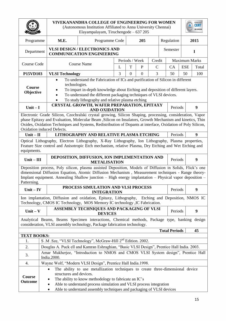
VIVEKANANDHA COLLEGE OF ENGINEERING FOR WOMEN (Autonomous Institution Affiliated to Anna University Chennai)
Elayampalayam, Tiruchengode – 637 205
Programme M.E. Programme Code 205 Regulation 2015
Department VLSI DESIGN / ELECTRONICS AND
COMMUNICATION ENGINEERING Semester
I
Course Code Course Name Periods / Week Credit Maximum Marks
L T P C CA ESE Total
P15VD103 VLSI Technology 3 0 0 3 50 50 100
Course
Objective
To understand the Fabrication of ICs and purification of Silicon in different
technologies.
To impart in-depth knowledge about Etching and deposition of different layers.
To understand the different packaging techniques of VLSI devices.
To study lithography and relative plasma etching
Unit – I CRYSTAL GROWTH, WAFER PREPARATION, EPITAXY
AND OXIDATION Periods 9
Electronic Grade Silicon, Czochralski crystal growing, Silicon Shaping, processing, consideration, Vapor
phase Epitaxy and Evaluation, Molecular Beam ,Silicon on Insulators, Growth Mechanism and kinetics, Thin
Oxides, Oxidation Techniques and Systems, Redistribution of Dopants at interface, Oxidation of Poly Silicon,
Oxidation induced Defects.
Unit – II LITHOGRAPHY AND RELATIVE PLASMA ETCHING Periods 9
Optical Lithography, Electron Lithography, X-Ray Lithography, Ion Lithography, Plasma properties,
Feature Size control and Anisotropic Etch mechanism, relative Plasma, Dry Etching and Wet Etching and
equipments.
Unit – III DEPOSITION, DIFFUSION, ION IMPLEMENTATION AND
METALISATION Periods 9
Deposition process, Poly silicon, plasma assisted Deposition, Models of Diffusion in Solids, Flick‟s one
dimensional Diffusion Equation, Atomic Diffusion Mechanism , Measurement techniques - Range theory-
Implant equipment. Annealing Shallow junction – High energy implantation – Physical vapor deposition –
Patterning.
Unit – IV PROCESS SIMULATION AND VLSI PROCESS
INTEGRATION Periods 9
Ion implantation, Diffusion and oxidation, Epitaxy, Lithography, Etching and Deposition, NMOS IC
Technology, CMOS IC Technology, MOS Memory IC technology ,IC Fabrication.
Unit – V ASSEMBLY TECHNIQUES AND PACKAGING OF VLSI
DEVICES Periods 9
Analytical Beams, Beams Specimen interactions, Chemical methods, Package type, banking design
consideration, VLSI assembly technology, Package fabrication technology.
Total Periods 45
TEXT BOOKS:
1. S .M .Sze, “VLSI Technology”, McGraw-Hill 2nd
Edition. 2002.
2. Douglas A. Puck ell and Kamran Eshraghian, “Basic VLSI Design”, Prentice Hall India. 2003.
3. Amar Mukherjee, “Introduction to NMOS and CMOS VLSI System design”, Prentice Hall
India.2000.
4. Wayne Wolf, “Modern VLSI Design”, Prentice Hall India.1998.
Course
Outcome
The ability to use metallization techniques to create three-dimensional device
structures and devices.
The ability to know methodology to fabricate an IC‟s
Able to understand process simulation and VLSI process integration
Able to understand assembly techniques and packaging of VLSI devices

16
VIVEKANANDHA COLLEGE OF ENGINEERING FOR WOMEN
(Autonomous Institution Affiliated to Anna University Chennai)
Elayampalayam, Tiruchengode – 637 205
Programme M.E. Programme Code 205 Regulation 2015
Department VLSI DESIGN / ELECTRONICS AND
COMMUNICATION ENGINEERING Semester I
Course Code Course Name Periods / Week Credit Maximum Marks
L T P C CA ESE Total
P15VD104 CMOS Analog VLSI Design 3 0 0 3 50 50 100
Course
Objectives
To study the basic CMOS analog circuits.
To understand the concept of Current Source, sink and Reference Circuits.
To design CMOS Amplifiers and converters.
To study IC packaging and process technology
Unit – I DYNAMIC ANALOG CIRCUITS Periods 9
MOSFET Small Signal Model-MOSFET as a Switch- Switched Capacitor Integrator-MOS Diode/Resistor-
Resistor Realization using Switched Capacitor-Switched Capacitor Filter- Comparator-D/A and A/D
Converter, PLL, Field Programmable Analog Array.
Unit – II CURRENT SOURCE-SINK AND REFERNCES Periods 9
The Current Mirror: The Cascode Connection-Sensitivity Analysis-Temperature Analysis-Transient
Response-Layout of the Simple Current Mirror-matching in MOSFET Mirrors-References: Voltage Dividers-
Current Source Self Biasing: Threshold Voltage Referenced Self-Biasing-Diode Referenced Self-Biasing-
Thermal Voltage Referenced Self Biasing-Band gap Voltage References-Beta Multiplier Referenced Self
Biasing.
Unit – III CMOS ANALOG AMPLIFIERS Periods 9
Amplifiers: Gate-Drain Connected Loads-Current Source Loads-Noise and Distortion in Amplifiers-Feedback
Amplifiers: Properties of Negative Feedback on Amplifier Design-Recognizing Feedback Topologies-
Voltage Amplifier- Transimpedance Amplifier –Transconductance Amplifier – Current Amplifier-Output
Amplifier -Cascode Amplifiers- Source Follower-Voltage Level Shifter-CMOS Operational Amplifier-
Differential Amplifier.
Unit – IV DATA CONVERTERS AND ARCHITECTURES Periods 9
Analog Versus Discrete Time Signals- S/H Characteristics- Mixed Signal Layout Issues-DAC Specifications
and Architectures: Digital Input Code- Resistor String-R-2R Ladder networks-Current Steering-Charge
Scaling DACs-Cyclic DAC- Pipeline DAC- ADC Specifications and Architectures: Flash-Two-Step Flash
ADC-Pipeline ADC-Integrating ADC-Successive Approximation ADC-Oversampling ADC.
Unit - V IC PACKAGING AND PROCESS TECHNOLOGY Periods 9
IC Packaging: Types and Modeling-Electrical Package Modeling- Thermal Modeling- Stress Modeling-
Package Simulation- Flip-Chip Package- VLSI Process Technology: Chrystal Growth- Photolithography-
Oxidation- Diffusion- Ion Implantation- Etching- Epitaxial Growth- Metallization- Packaging.
Total Periods 45
REFERENCES:
1. R. Jacob Baker, Harry W. Li, David E. Boyce, “CMOS Circuit Design, Layout and Simulation”,
IEEE Press Series on Microelectronics Systems Stuart K. Tewksbuy, Series Edition.
2. Debaprasad Das, “VLSI Design” Oxford University Press.
3. Neil H. E. Weste, David Harris, Ayan Banerjee, "CMOS VLSI Design”, Pearson, 3rd
Edition.
4. Malcom R.Haskard, LanC.May,“AnalogVLSIDesign- NMOSandCMOS",PrenticeHall,1998.

17
Course
Outcome
Able to
Analyze various types of amplifiers used in analog VLSI design
Identify the issues in dynamic analog circuits
Classify CMOS Amplifiers and converters
analyze feedback amplifiers
18
VIVEKANANDHA COLLEGE OF ENGINEERING FOR WOMEN
(Autonomous Institution Affiliated to Anna University Chennai)
Elayampalayam, Tiruchengode – 637 205
Programme M.E. Programme Code 205 Regulation 2015
Department VLSI DESIGN / ELECTRONICS AND
COMMUNICATION ENGINEERING Semester
I
Course Code Course Name
Periods / Week Credit Maximum Marks
L T P C CA ESE Total
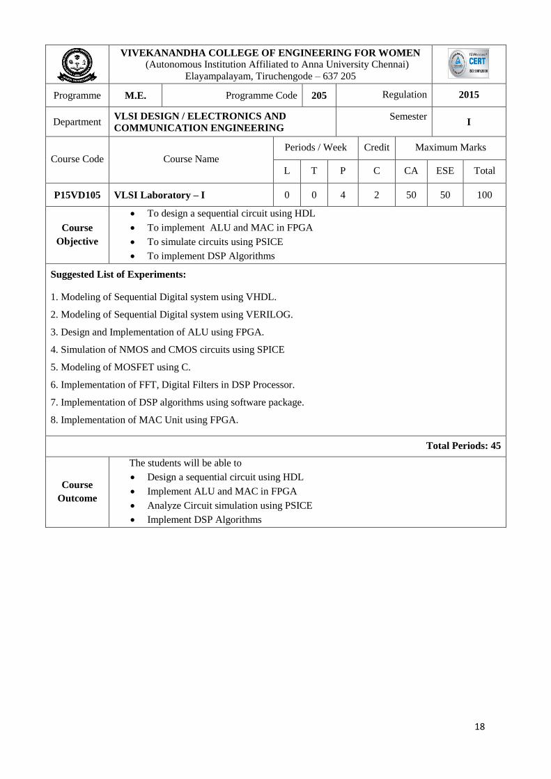
P15VD105 VLSI Laboratory – I 0 0 4 2 50 50 100
Course
Objective
To design a sequential circuit using HDL
To implement ALU and MAC in FPGA
To simulate circuits using PSICE
To implement DSP Algorithms
Suggested List of Experiments:
1. Modeling of Sequential Digital system using VHDL.
2. Modeling of Sequential Digital system using VERILOG.
3. Design and Implementation of ALU using FPGA.
4. Simulation of NMOS and CMOS circuits using SPICE
5. Modeling of MOSFET using C.
6. Implementation of FFT, Digital Filters in DSP Processor.
7. Implementation of DSP algorithms using software package.
8. Implementation of MAC Unit using FPGA.
Total Periods: 45
Course
Outcome
The students will be able to
Design a sequential circuit using HDL
Implement ALU and MAC in FPGA
Analyze Circuit simulation using PSICE
Implement DSP Algorithms

19
VIVEKANANDHA COLLEGE OF ENGINEERING FOR WOMEN
(Autonomous Institution Affiliated to Anna University Chennai)
Elayampalayam, Tiruchengode – 637 205
Programme M.E. Programme Code 205 Regulation 2015
Department VLSI DESIGN / ELECTRONICS AND
COMMUNICATION ENGINEERING Semester II
Course Code Course Name Periods / Week Credit Maximum Marks
L T P C CA ESE Total
P15VD206 Low Power VLSI Design 3 0 0 3 50 50 100
Course
Objective
To study the principle of low power design.
To explore the concept of power optimization and estimation analysis.
To understand the layout design and special techniques.
To study the software design for low power techniques.
Unit - I POWER DISSIPATION IN CMOS Periods 9
Hierarchy of limits of power – Sources of power consumption – Physics of power dissipation in CMOS FET
devices- Basic principle of low power design.
Unit - II POWER OPTIMIZATION Periods 9
Logical level power optimization – Circuit level low power design – Circuit techniques for reducing power
consumption in adders and multipliers.
Unit - III DESIGN OF LOW POWER CMOS CIRCUITS Periods 9
Computer Arithmetic techniques for low power systems – Reducing power consumption in memories – Low
power clock, Interconnect and layout design – Advanced techniques – Special techniques.
Unit - IV POWER ESTIMATION Periods 9
Power estimation techniques – Logic level power estimation – Simulation power analysis– Probabilistic
power analysis.
Unit - V SYNTHESIS AND SOFTWARE DESIGN FOR LOW
POWER Periods 9
Synthesis for low power –Behavioral level transforms- Software design for low power
Total Periods 45
REFERENCES:
1. K.Roy & S.C. Prasad, “Low Power CMOS VLSI Circuit Design” Wiley, 2000.
2. Dimitrios Soudris, Chirstian Pignet, Costas Goutis, “Designing CMOS Circuits for Low Power”,
Kluwer Academic Publishers, 2002.
3. J.B. Kuo and J.H Lou, “Low Voltage CMOS VLSI Circuits, Wiley 1999.
4. A.P.Chandrakasan and R.W. Broadersen, “Low Power Digital CMOS Design”, Kluwer
Academic Publishers 1995.
5. Gary Yeap, “Practical Low Power Digital VLSI Design”, Kluwer, 1998.
6. Abdellatif Bellaouar, Mohamed.I. Elmasry, “Low Power Digital VLSI Design”, Kluwer
Academic Publishers 1995.
7. James B. Kuo, Shin – chia Lin, “Low Voltage SOI CMOS VLSI Devices and Circuits”. John
Wiley & sons, Inc 2001.
Course
Outcome
The students will be able to
Design logic circuit layouts for both static CMOS and dynamic clocked CMOS circuits
Extract the analog parasitic elements from the layout
Analyze the circuit timing using a logic simulator and an analog simulator .
Design a software for low power

20
VIVEKANANDHA COLLEGE OF ENGINEERING FOR
WOMEN (Autonomous Institution Affiliated to Anna University
Chennai)
Elayampalayam, Tiruchengode – 637 205
Programme M.E. Programme Code 205 Regulation 2015
Department VLSI DESIGN / ELECTRONICS AND
COMMUNICATION ENGINEERING Semester II
Course Code Course Name
Periods / Week Credit Maximum Marks
L T P C CA ESE Total
P15VD207 Testing and Verification of VLSI
Circuits 3 0 0 3 50 50 100
Course
Objective
To study the fault modeling and detection techniques.
To understand the test generation for combinational and sequential logic circuits.
To explore the design for testability and self test methods.
To study the fault diagnosis
Unit – I FUNDAMENTALS OF TESTING Periods 9
Scope of testing and verification in VLSI design process. Issues in test and verification of complex chips,
embedded cores and SOCs; Fundamentals of VLSI testing.
Unit – II TEST GENERATION AND SIMLUATION Periods 9
Automatic test pattern generation. Design for testability. Scan design. Test interface and boundary scan.
System testing and test for SOCs. Iddq testing.
Unit – III FAULT MODELS Periods 9
Fault models: Delay fault testing. BIST for testing of logic and memories. Test automation.
Unit – IV DESIGN AND VERIFICATION OF VLSI CIRCUITS Periods 9
Design verification techniques based on simulation, Analytical and Formal approaches. Functional
verification of VLSI circuits.
Unit – V TIMING VERIFICATION OF VLSI CIRCUITS Periods 9
Timing verification. Formal verification. Basics of equivalence checking and model checking. Hardware
emulation.
Total Periods 45
REFERENCES:
1. M. Bushnell and V. D. Agrawal, "Essentials of Electronic Testing for Digital”, Memory and
Mixed-Signal VLSI Circuits", Kluwer Academic Publishers, 2000.
2. M. Abramovici, M. A. Breuer and A. D. Friedman, "Digital Systems Testing and Testable
Design", IEEE Press, 1990.
3. T.Kropf, "Introduction to Formal Hardware Verification", Springer Verlag, 2000.
4. P. Rashinkar, Paterson and L. Singh, "System-on-a-Chip Verification-Methodology and
Techniques", Kluwer Academic Publishers, 2001.
Course
Outcome
Able to
Insert elementary testing hardware into the VLSI chip
Analyze VLSI circuit timing using Logical Effort analysis
Estimate and compute the power consumption of a VLSI chip
Understand the concept of test generation and simulation

21
VIVEKANANDHA COLLEGE OF ENGINEERING FOR WOMEN
(Autonomous Institution Affiliated to Anna University ,Chennai)
Elayampalayam, Tiruchengode – 637 205
Programme M.E. Programme code 205 Regulation 2015
Department ME-CSE, ME- PSE, ME- VLSI & M. Tech- IT Semester II
Course code Course Name Periods / Week Credit Maximum Marks
L T P C CA ESE Total
P15VD208 Research Methodology and Data
Analysis 3 0 0 3 50 50 100
Course
Objective
To understand the importance of Research
To acquire knowledge in Data Collection and Analysis of Data
To effectively write reports
Unit – I INTRODUCTION TO RESEARCH Periods 7
Nature, scope, and design of social research; Review of literature: qualitative (literary), quantitative (meta-
analysis)
Unit – II HYPOTHESIS Periods 9
Hypothesis: sources, types and characteristics; Sample survey: sample and census survey, probability, non-
probability and mixed sampling
Unit – III DATA COLLECTION Periods 11
Methods of data collection: historical method, case study, observation, ethnographic methods, interview,
questionnaire, focus group discussion, participatory rural appraisal, experimental method, pre-testing, and
pilot survey; Scaling techniques different scales, item analysis, reliability, validity; Method of secondary data
collection: sources, sample criteria, characteristics.
Unit – IV DATA ANALYSIS Periods 9
Data analysis: descriptive statistics, mean difference test, analysis of variance and experimental design;
Bivariate and multivariate correlation and regression; Factor analysis, Cluster analysis, Discriminant analysis,
Structural equation modelling, non-parametric statistics, Content analysis
Unit – V REPORT WRITING Periods 9
Report writing: review, qualitative, and empirical article writing.
Total Periods 45
REFERENCES:
1. C.M.Chaudhary, “Research Methodology”, RBSA Publishers, Jaipur, India 2009.
2. R.Paneerselvam, “Research Methodology”, PHI Learning Pvt Ltd., New Delhi 2009.
Course
Outcome
Can formulate researchable questions
Can define a research strategy and design a research project to answer a research
question
Can discuss the practice and principles of qualitative and quantitative social research
22
VIVEKANANDHA COLLEGE OF ENGINEERING FOR
WOMEN (Autonomous Institution, Affiliated to Anna University
,Chennai)
Elayampalayam, Tiruchengode – 637 205 Programme M.E. Programme Code 205 Regulation 2015
Department VLSI DESIGN / ELECTRONICS AND
COMMUNICATION ENGINEERING Semester II
Course Code Course Name
Periods / Week Credit Maximum Marks
L T P C CA ESE Total
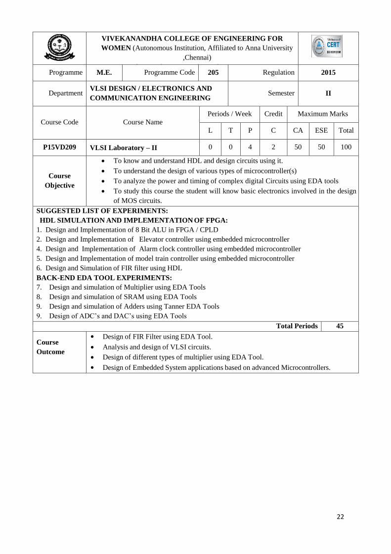
P15VD209 VLSI Laboratory – II 0 0 4 2 50 50 100
Course
Objective
To know and understand HDL and design circuits using it.
To understand the design of various types of microcontroller(s)
To analyze the power and timing of complex digital Circuits using EDA tools
To study this course the student will know basic electronics involved in the design
of MOS circuits.
SUGGESTED LIST OF EXPERIMENTS:
HDL SIMULATION AND IMPLEMENTATION OF FPGA:
1. Design and Implementation of 8 Bit ALU in FPGA / CPLD
2. Design and Implementation of Elevator controller using embedded microcontroller
4. Design and Implementation of Alarm clock controller using embedded microcontroller
5. Design and Implementation of model train controller using embedded microcontroller
6. Design and Simulation of FIR filter using HDL
BACK-END EDA TOOL EXPERIMENTS:
7. Design and simulation of Multiplier using EDA Tools
8. Design and simulation of SRAM using EDA Tools
9. Design and simulation of Adders using Tanner EDA Tools
9. Design of ADC‟s and DAC‟s using EDA Tools
Total Periods 45
Course
Outcome
Design of FIR Filter using EDA Tool.
Analysis and design of VLSI circuits.
Design of different types of multiplier using EDA Tool.
Design of Embedded System applications based on advanced Microcontrollers.

23
VIVEKANANDHA COLLEGE OF ENGINEERING FOR
WOMEN (Autonomous Institution Affiliated to Anna University
Chennai)
Elayampalayam, Tiruchengode – 637 205
Programme M.E. Programme Code 205 Regulation 2015
Department VLSI DESIGN / ELECTRONICS AND
COMMUNICATION ENGINEERING Semester -
Course Code Course Name
Periods / Week Credit Maximum Marks
L T P C CA ESE Total
P15VDE01 Simulation of Circuits and
Devices 3 0 0 3 50 50 100
Course
Objective
To understand different types of network
To study memory mesh analysis.
To study semiconductor devices.
To study FET technologies.
Unit – I NODAL ANALYSIS Periods 9
Formulation of network equations: Nodal, mesh, modified nodal and hybrid analysis equations. Sparse matrix
techniques; Solution of nonlinear networks through Newton-Raphson technique.
Unit – II NETWORK ANALYSIS Periods 9
Multistep methods: convergence and stability; Special classes of multistep methods: Adams-bashforth,
Adams-Moulton and Gear's methods; Solution of stiff systems of equations; Adaptation of multistep methods
to the solution of electrical networks.
Unit – III SEMICONDUCTORS Periods 9
Semiconductors General purpose circuit simulators. Review of semiconductor equations (Poisson,
continuity, drift-diffusion, trap rate). Finite difference formulation of these equations in 1D and 2D. Grid
generation. General purpose circuit simulators. Review of semiconductor equations (Poisson, continuity,
drift-diffusion, trap rate). Finite difference formulation of these equations in 1D and 2D. Grid generation.
Unit – IV SMALL SIGNAL ANALYSIS Periods 9
Computation of characteristics of simple devices (p-n junction, MOS capacitor, MOSFET, etc.); Small-
signal analysis.
Unit – V FET TECHNOLOGIES Periods 9
High-current and high- frequency effects; Heterojunction bipolar transistors; Junction FETs; JFET, MESFET
and heterojunction FET.
Total Periods 45
REFERENCES:
1. L.O.Chua & P.M.Lin, “Computer aided analysis and electronic circuits”, Prentice Hall, 1975.
2. S. Selberherr, “Analysis and Simulation of Semiconductor Devices”, Springer-Verlag, 1984.
3. N.J. McCalla, “Fundamentals of Computer Aided Circuit Simulation”, Kluwer Academic
Publishers, 1988.
Course
Outcome
The students will be able to
Compare the working principle of various types of semiconductor
Analyze the small signal amplifiers
Understand nodal analysis and network analysis
Know basic definitions and properties associated with semiconductors.

24
VIVEKANANDHA COLLEGE OF ENGINEERING FOR WOMEN
(Autonomous Institution Affiliated to Anna University ,Chennai)
Elayampalayam, Tiruchengode – 637 205
Programme M.E. Programme code 205 Regulation 2015
Department VLSI DESIGN / ELECTRONICS AND
COMMUNICATION ENGINEERING Semester -
Course code Course Name Periods / Week Credit Maximum Marks
L T P C CA ESE Total
P15VDE02 Hardware Design Verification
Techniques 3 0 0 3 50 50 100
Course
Objective
To understand the Concepts of Verification Techniques and Tools.
To study the concepts of Verification Plan, Stimulus and Response.
To understand the concepts of Architecting Test benches and System Verilog.
To impart in-depth knowledge about RTL design.
Unit – I VERIFICATION TECHNIQUES AND TOOLS Periods 9
Testing vs. Verification – Verification and Design Reuse - Functional Verification, Timing Verification,
FormalVerification, Linting Tools – Simulators – Third Party Models – Waveform Viewers – Code
Coverage issue–Tracking Metrics.
Unit – II VERIFICATION PLAN Periods 9
Verification plan – Levels of Verification – Verification Strategies – Specification Features – Test cases
– Test Benches
Unit – III STIMULUS AND RESPONSE Periods 9
Simple Stimulus – Output Verification – Self Checking Test Benches – Complex Stimulus and
Response –Prediction of Output
Unit – IV ARCHITECTING TEST BENCHES Periods 9
Reusable Verification Components – VHDL and Verilog Implementation – Autonomous Generation and
Monitoring– Input and Output Paths –– Verifying Configurable Design.
Unit – V SYSTEM VERILOG Periods 9
Data types, RTL design, Interfaces, clocking, Assertion based verification, classes, Test bench
automation and constraints.
Total Periods 45
REFERENCES:
1 Janick Bergeron, “Writing Test Benches Functional Verification of HDL Models”, Springer,
2003.
2 Andreas Meyer, “Principles of Functional Verification”, Newnes, 2003.
3 Samir Palnitkar, “Design Verification with E”, Prentice Hall, 2003.
4 T.Kropf, “Introduction to Formal Hardware Verification”, Springer Verlag, 2010.
5 Chris Spear, “ System Verilog for Verification: A Guide to Learning the Test bench
Language Features”, Springer, 2008
6 Janick Bergeron, Edward Cerny, Alan Hunter and Andrew Nightingale, “Verification
Methodology Manual for System Verilog”, Springer, 2005.
Course
Outcome
Able to analyze and design small scale combinational logic circuits using HDLs.
Able to analyze the problems in digital design using HDLs.
Able to view VLSI design from a hierarchical viewpoint.
Select appropriate analysis for circuit design

25
VIVEKANANDHA COLLEGE OF ENGINEERING FOR WOMEN
(Autonomous Institution Affiliated to Anna University Chennai)
Elayampalayam, Tiruchengode – 637 205
Programme M.E. Programme Code 205 Regulation 2015
Department VLSI DESIGN / ELECTRONICS AND
COMMUNICATION ENGINEERING Semester -
Course Code Course Name Periods / Week Credit Maximum Marks
L T P C CA ESE Total
P15VDE03 Advanced Digital Signal
Processing 3 0 0 3 50 50 100
Course
Objective
To introduce advanced digital signal processing techniques
To explore the concepts of multi rate signal processing and multi rate filters.
To study the adaptive filters and its applications.
To learn fundamental concepts on signal processing in power spectrum estimation.
Unit – I MULTIRATE SIGNAL PROCESSING Periods 9
Introduction-Sampling and Signal Reconstruction-Sampling rate conversion – Decimation by an integer
factor – Interpolation by an integer factor –Sampling rate conversion by a rational factor –poly-phase FIR
structures – FIR structures with time varying coefficients - Sampling rate conversion by a rational factor-
Multistage design of decimator and interpolator.
Unit – II MULTIRATE FIR FILTER DESIGN Periods 9
Design of FIR filters for sampling rate conversion –Applications of Interpolation and decimation in signal
processing –Filter bank implementation –Two channel filter banks-QMF filter banks –Perfect Reconstruction
Filter banks – tree structured filter banks - DFT filter Banks – M-channel filter banks- octave filter banks
Unit – III ADAPTIVE FILTERS Periods 9
FIR Adaptive filters - Newton's steepest descent method – Adaptive filters based on steepest descent method -
LMS Adaptive algorithm – other LMS based adaptive filters- RLS Adaptive filters - Exponentially weighted
RLS - Sliding window RLS - Simplified IIR LMS Adaptive filter-Applications: Adaptive channel
equalization - Adaptive echo canceller - Adaptive noise cancellation.
Unit – IV POWER SPECTRAL ESTIMATION Periods 9
Estimation of spectra from finite duration observations of a signal –The Periodogram-Use of DFT in Power
spectral Estimation –Non Parametric methods for Power spectrum Estimation – Bartlett. Welch and
Blackman–Tukey methods –Comparison of performance of Non Parametric power spectrum Estimation
methods – Application: speech enhancement using power spectrum estimation
Unit – V PARAMETRIC METHODS OF POWER SPECTRUM
ESTIMATION Periods 9
Relationship between auto correlation and model parameters – AR (Auto –Regressive) process and Linear
prediction –Yule –Walker, Burg & Unconstrained Least squares methods –Moving average (MA) and ARMA
Models – Minimum variance method –Pisarenko‟s harmonic De composition Method – MUSIC method.
Total Periods 45
REFERENCES:
1. H. Monson Hayes, “Statistical Digital Signal Processing and Modeling”, John Wiley and Sons, Inc.,
2008.
2. G. John Proakis and G. Dimitris Manolakis, “Digital Signal Processing”, Pearson Education, 2006.
3. P.P.Vaidyanathan , “Multirate Syatems and Filter Banks”, Pearson Education, 2008.
4. N.J.Filege, “Multirate Digital Signal Processing”, John Wiley and Sons, 2000.
5. G..John Proakis, “Algorithms for Statistical Signal Processing”, Pearson Education, 2002.
6. G.Dimitris and G.Manolakis., “Statistical and Adaptive Signal Processing”, McGraw Hill, 2002.
7. Sophoncles J. Orfanidis, “Optimum Signal Processing”, McGraw Hill, 2007.

26
Course
Outcome
Acquiring knowledge of how a multi rate system works.
Ability to design and implement decimator and interpolator and to design multi rate
filter bank.
Understanding different spectral estimation techniques and linear prediction.
Ability to design LMS and RLS adaptive filters for signal enhancement, channel
equalization.
27
VIVEKANANDHA COLLEGE OF ENGINEERING FOR
WOMEN (Autonomous Institution Affiliated to Anna University
Chennai)
Elayampalayam, Tiruchengode – 637 205
Programme M.E. Programme Code 205 Regulation 2015
Department VLSI DESIGN / ELECTRONICS AND
COMMUNICATION ENGINEERING Semester -
Course Code Course Name
Periods / Week Credit Maximum Marks
L T P C CA ESE Total
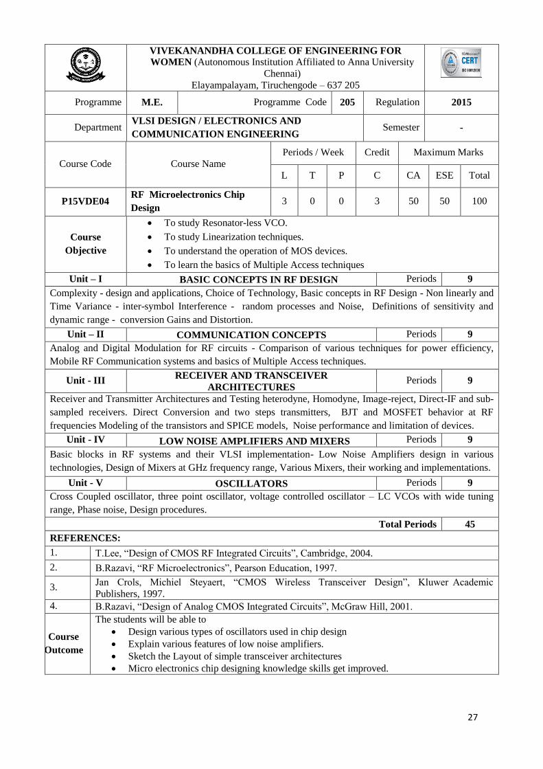
P15VDE04 RF Microelectronics Chip
Design 3 0 0 3 50 50 100
Course
Objective
To study Resonator-less VCO.
To study Linearization techniques.
To understand the operation of MOS devices.
To learn the basics of Multiple Access techniques
Unit – I BASIC CONCEPTS IN RF DESIGN Periods 9
Complexity - design and applications, Choice of Technology, Basic concepts in RF Design - Non linearly and
Time Variance - inter-symbol Interference - random processes and Noise, Definitions of sensitivity and
dynamic range - conversion Gains and Distortion.
Unit – II COMMUNICATION CONCEPTS Periods 9
Analog and Digital Modulation for RF circuits - Comparison of various techniques for power efficiency,
Mobile RF Communication systems and basics of Multiple Access techniques.
Unit - III RECEIVER AND TRANSCEIVER
ARCHITECTURES Periods 9
Receiver and Transmitter Architectures and Testing heterodyne, Homodyne, Image-reject, Direct-IF and sub-
sampled receivers. Direct Conversion and two steps transmitters, BJT and MOSFET behavior at RF
frequencies Modeling of the transistors and SPICE models, Noise performance and limitation of devices.
Unit - IV LOW NOISE AMPLIFIERS AND MIXERS Periods 9
Basic blocks in RF systems and their VLSI implementation- Low Noise Amplifiers design in various
technologies, Design of Mixers at GHz frequency range, Various Mixers, their working and implementations.
Unit - V OSCILLATORS Periods 9
Cross Coupled oscillator, three point oscillator, voltage controlled oscillator – LC VCOs with wide tuning
range, Phase noise, Design procedures.
Total Periods 45
REFERENCES:
1. T.Lee, “Design of CMOS RF Integrated Circuits”, Cambridge, 2004.
2. B.Razavi, “RF Microelectronics”, Pearson Education, 1997.
3. Jan Crols, Michiel Steyaert, “CMOS Wireless Transceiver Design”, Kluwer Academic
Publishers, 1997.
4. B.Razavi, “Design of Analog CMOS Integrated Circuits”, McGraw Hill, 2001.
Course
Outcome
The students will be able to
Design various types of oscillators used in chip design
Explain various features of low noise amplifiers.
Sketch the Layout of simple transceiver architectures
Micro electronics chip designing knowledge skills get improved.

28
VIVEKANANDHA COLLEGE OF ENGINEERING FOR
WOMEN (Autonomous Institution Affiliated to Anna University
Chennai)
Elayampalayam, Tiruchengode – 637 205
Programme M.E. Programme Code 205 Regulation 2015
Department VLSI DESIGN / ELECTRONICS AND
COMMUNICATION ENGINEERING Semester -
Course Code Course Name
Periods / Week Credit Maximum Marks
L T P C CA ESE Total
P15VDE05 Physics of MOS Transistors 3 0 0 3 50 50 100
Course
Objective
To provide an in-depth knowledge in VLSI Design methodology.
To enhance the fundamentals of different scaling rules.
To study NANO MOS transistors
To study properties of optical receiver
Unit – I MOS TRANSISTORS Periods 9
The MOS transistor: Pao-Sah and Brews models; Short channel effects in MOS transistors. Hot-carrier effects
in MOS transistors; Quasi-static compact models of MOS transistors; Measurement of MOS transistor
parameters.
Unit – II SCALING RULES Periods 9
Scaling and transistors structures for ULSI; Silicon-on-insulator transistors; High-field and radiation effects in
transistors, The bipolar transistor.
Unit – III SMALL SIGNAL ANALYSIS Periods 9
Ebers-Moll model; charge control model; small-signal and switching characteristics; Graded-base and graded-
emitter transistors; High-current and high- frequency effects; Hetero junction bipolar transistors; Junction
FETs; JFET, MESFET and hetero junction FET.
Unit – IV NANO MOS TRANSISTOR Periods 9
Schrödinger equation, states and operators, particle-in-a-box, density-of-states, harmonic oscillator, hydrogen
atom, tunneling, two-level systems. Electrons in a crystal lattice, quantum well, wire and dot devices.
Unit – V OPTICAL PROPERTIES Periods 9
Maxwell‟s equations in dielectric media, polarization in insulators, ferroelectrics, polarons and polaritons,
direct and indirect transitions in semiconductors, excitons, optoelectronic and photovoltaic devices.
Total Periods 45
REFERENCES:
1. R.M.Warner , B.L.Grung , “ MOSFET – Theory and Design” Published by Oxford
University Press, 1999.
2. Y.Tsividis, “ Operation and Modeling of the MOSFET”, TMH publication
3. Simon M. Sze, Kwe K. Ng, “ Physics of Semiconductor Devices” Wiley 3rd
Edition.
4. P.I.Varghese, T. Pradeep, A.Ashok Reddy, “A Text Book of Nanoscience and
Nanotechnology”.
Course
Outcome
Students will be able to
Analyze a NANO MOS transistor model.
Design and analyzis of circuits in different scaling.
Analyze small signal transistor
Understand different optical properties

29
VIVEKANANDHA COLLEGE OF ENGINEERING FOR WOMEN
(Autonomous Institution Affiliated to Anna University Chennai)
Elayampalayam, Tiruchengode – 637 205
Programme M.E. Programme Code 205 Regulation 2015
Department VLSI DESIGN / ELECTRONICS AND
COMMUNICATION ENGINEERING Semester -
Course Code Course Name Periods / Week Credit Maximum Marks
L T P C CA ESE Total
P15VDE06 VLSI Design 3 0 0 3 50 50 100
Course
Objective
To understand the concepts of NMOS and PMOS transistors.
To understand the Basic CMOS technology.
To study the Multiplexers.
To understand the concepts of digital design with Verilog HDL.
Unit – I MOS TRANSISTOR THEORY Periods 9
NMOS Enhancement Transistor and PMOS Enhancement transistors, Threshold voltage- Body effect- MOS
device design equations-MOS Models-Small signal AC characteristics-Complementary CMOS Inverter-DC
Characteristics-Static Load MOS Inverters.
Unit – II CMOS PROCESSING TECHNOLOGY AND LOGIC
DESIGN Periods 9
Silicon Semiconductor Technology- overview- Basic CMOS technology-CMOS process Enhancements:
Interconnect –Circuit Elements-Layout Design Rules-Latch UP- Switch Logic-Design of ALU subsystem-
Design of Manchester Carry Chain.
Unit – III CIRCUIT CHARACTERISATION AND PERFORMANCE
ESTIMATION Periods 9
Resistance estimation, Capacitance estimation, Inductance, switching characteristics, CMOS –Gate transistor
sizing, power dissipation and design margining, Charge sharing ,Yield and Reliability-Scaling of MOS
transistor.
Unit – IV SUBSYSTEM DESIGN AND LAYOUT Periods 9
Gate logic-Combinational Logic-Clocked Sequential Circuits-Precharged Bus Concept-Power dissipation for
CMOS and BICMOS circuits-Design of 4-bit arithmetic Processor-Design of 4-bit Shifter-Memory
elements-Finite State Machines.
Unit – V VERILOG HARDWARE DESCRIPTION LANGUAGE Periods 9
Overview of digital design with Verilog HDL, hierarchical modeling concepts, modules and port definitions,
gate level modeling, data flow modeling, behavioral modeling, task & functions, Test Bench.
Total Periods 45
REFERENCES:
1. N. Weste and K. Eshranghian, “Principles of CMOS VLSI Design”, Addison Wesley. 1985
2. Douglas.A.Pucknell Kamran Eshranghian, “Basic VLSI Design”, 3rd Edition, 1994.
3. Samir Palnitkar, “Verilog HDL”, Pearson Education, 2nd
Edition, 2004.
4. Eugene D.Fabricius, “Introduction to VLSI Design”, McGraw Hill International Editions, 1990.
Course
Outcome
Able to understand the concepts of NMOS and PMOS transistors.
Able to understand the Basic CMOS technology.
Able to understand the concepts of digital design with Verilog HDL.
• Understand the concepts of digital design with Verilog HDL.
30
VIVEKANANDHA COLLEGE OF ENGINEERING FOR WOMEN
(Autonomous Institution Affiliated to Anna University Chennai)
Elayampalayam, Tiruchengode – 637 205
Programme M.E. Programme Code 205 Regulation 2015
Department VLSI DESIGN / ELECTRONICS AND
COMMUNICATION ENGINEERING Semester -
Course Code Course Name
Periods Per Week Credit Maximum Marks
L T P C CA ESE Total
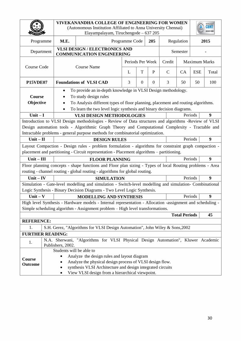
P15VDE07 Foundations of VLSI CAD 3 0 0 3 50 50 100
Course
Objective
To provide an in-depth knowledge in VLSI Design methodology.
To study design rules
To Analysis different types of floor planning, placement and routing algorithms.
To learn the two level logic synthesis and binary decision diagrams.
Unit – I VLSI DESIGN METHODOLOGIES Periods 9
Introduction to VLSI Design methodologies - Review of Data structures and algorithms -Review of VLSI
Design automation tools - Algorithmic Graph Theory and Computational Complexity - Tractable and
Intractable problems - general purpose methods for combinatorial optimization.
Unit – II DESIGN RULES Periods 9
Layout Compaction - Design rules - problem formulation - algorithms for constraint graph compaction -
placement and partitioning - Circuit representation - Placement algorithms – partitioning.
Unit – III FLOOR PLANNING Periods 9
Floor planning concepts - shape functions and Floor plan sizing - Types of local Routing problems - Area
routing - channel routing - global routing - algorithms for global routing.
Unit – IV SIMULATION Periods 9
Simulation - Gate-level modelling and simulation - Switch-level modelling and simulation- Combinational
Logic Synthesis - Binary Decision Diagrams - Two Level Logic Synthesis.
Unit – V MODELLING AND SYNTHESIS Periods 9
High level Synthesis - Hardware models - Internal representation - Allocation -assignment and scheduling -
Simple scheduling algorithm - Assignment problem – High level transformations.
Total Periods 45
REFERENCE:
1. S.H. Gerez, "Algorithms for VLSI Design Automation", John Wiley & Sons,2002
FURTHER READING:
1. N.A. Sherwani, "Algorithms for VLSI Physical Design Automation", Kluwer Academic
Publishers, 2002.
Course
Outcome
Students will be able to
Analyze the design rules and layout diagram
Analyze the physical design process of VLSI design flow.
synthesis VLSI Architecture and design integrated circuits
View VLSI design from a hierarchical viewpoint.
31
VIVEKANANDHA COLLEGE OF ENGINEERING FOR WOMEN
(Autonomous Institution Affiliated to Anna University Chennai)
Elayampalayam, Tiruchengode – 637 205
Programme M.E. Programme Code 205 Regulation 2015
Department VLSI DESIGN / ELECTRONICS AND
COMMUNICATION ENGINEERING Semester -
Course Code Course Name Periods / Week Credit Maximum Marks
L T P C CA ESE Total
P15VDE08 Wavelets and Sub Band Coding 3 0 0 3 50 50 100
Course
Objective
To understand the Fourier analyze
To study continuous Wavelet Transform & Multi Resolution Analysis
To understand Multi Rate systems
To study applications of Wavelets
Unit – I FOURIER ANALYSIS Periods 9
Signal spaces - concept of Convergence - Hilbert spaces for energy signals. Fourier basis & Fourier
Transform – failure of Fourier Transform – Need for Time-Frequency Analysis, Spectrogram plot - Phase-
Space plot in Time-Frequency plane, Time and Frequency Limitations, Tiling of the Time-Frequency Plane
for STFT – Heisenberg‟s Uncertainty principle – Short time Fourier transform (STFT) Analysis- short
comings of STFT- Need for Wavelets.
Unit – II CONTINUOUS WAVELET TRANSFORM(CWT) AND
MULTI RESOLUTION ANALYSIS (MRA) Periods 9
Wavelet basis – concept of scale and its relation with frequency, Continuous time Wavelet Transform
equation – series expansion using wavelets – CWT – need for scaling function – Multi-Resolution Analysis
(MRA) –- Tiling of time-scale plane for CWT. Important wavelets: Haar, Mexican hat, Meyer, Shannon,
Daubechies
Unit – III MULTIRATE SYSTEMS, FILTER BANKS AND
DISCRETE WAVELET TRANSFORM (DWT) Periods 9
Decimation and Interpolation in Time domain - Decimation and Interpolation in Frequency domain – Multi
rate systems for a rational factor, Two channel filter bank – Perfect Reconstruction (PR) condition –
relationship between filter banks and wavelet basis – DWT – Filter banks for Daubechies wavelet function.
Unit – IV SPECIAL TOPICS Periods 9
Wavelet packet transforms Multidimensional wavelets, Bi-orthogonal basis-B-Splines, Lifting scheme of
wavelet generation, Multiwavelets.
Unit – V APPLICATIONS OF WAVELETS Periods 9
Signal Denoising - Sub-band coding of Speech and music– Image Compression using 2-D DWT- Fractal
Signal Analysis.
Total Periods 45
REFERENCES:
1. Jaideva C Goswami and Andrew K Chan, “Fundamentals of Wavelets – Theory, Algorithms and
Applications”, John Wiley and Sons, Inc., Singapore, 1999.
2. Soman K P and Ramachandran K I, “Insight into Wavelets from Theory to Practice”, Prentice Hall
India, First Edition, 2004.
3. Vetterli M, and Kovacevic J, "Wavelets and Subband Coding," Prentice Hall, 1995.
4. Fliege. N J, “Multirate Digital Signal Processing”, John Wiley and Sons, Newyork, 1994.
5. Stephane G Mallat, “A Wavelet Tour of Signal Processing”, Academic Press, 2nd
Edition, 1999.

32
6. Wornell G W, "Signal Processing with Fractals: A Wavelet Based Approach”, Prentice Hall, 1995.
Course
Outcome
Able to understand the Fourier analyze
Able to Understand the CWT & MRA
Comprehend Multi Rate systems
Understand the applications of Wavelets

33
VIVEKANANDHA COLLEGE OF ENGINEERING FOR WOMEN
(Autonomous Institution, Affiliated to Anna University ,Chennai)
Elayampalayam, Tiruchengode – 637 205
Programme M.E. Programme Code 205 Regulation 2015
Department VLSI DESIGN / ELECTRONICS AND
COMMUNICATION ENGINEERING Semester -
Course Code Course Name Periods / Week Credit Maximum Marks
L T P C CA ESE Total
P15VDE09 Embedded System Design 3 0 0 3 50 50 100
Course
Objective
To study the overview of Embedded System Architecture
To provide an in-depth knowledge of embedded system Design.
To study the interfacing Concepts.
To study the design of Software.
Unit - I EMBEDDED DESIGN LIFE CYCLE Periods 09
Product specification – Hardware / Software partitioning – Detailed hardware and software design –
Integration – Product testing – Selection Processes – Microprocessor Vs Micro Controller – Performance tools –
Bench marking – RTOS Micro Controller – Performance tools – Bench marking – RTOS availability – Tool
chain availability – Other issues in selection processes.
Unit - II PARTITIONING DECISION Periods 09
Hardware / Software duality – coding Hardware – ASIC revolution – Managing the Risk – Co-verification –
execution environment – memory organization – System startup – Hardware manipulation – memory
mapped access – speed and code density.
Unit – III INTERRUPT SERVICE ROUTINES Periods 09
Watch dog timers – Flash Memory basic toolset – Host based debugging – Remote debugging – ROM emulators
– Logic analyzer – Caches – Computer optimization – Statistical profiling
Unit – IV IN CIRCUIT EMULATORS Periods 09
Bullet proof run control – Real time trace – Hardware break points – Overlay memory – Timing constraints –
Usage issues – Triggers.
Unit - V TESTING Periods 09
Bug tracking – reduction of risks & costs – Performance – Unit testing – Regression testing – Choosing test
cases – Functional tests – Coverage tests – Testing embedded software – Performance testing – Maintenance.
Total Periods 45
REFERENCES:
1 Arnold S. Berger – “Embedded System Design”, CMP books, USA 2002.
2 J.W. Valvano, "Embedded Microcomputer System: Real Time Interfacing", Brooks/Cole, 2000
3 ARKIN, R.C., “Behaviour-based Robotics”, The MIT Press, 1998
4 Sriram Iyer, “Embedded Real time System Programming”
Course To understand the embedded Design life cycle.

34
Outcome To analyze partition decision and interrupt service routine
Able to analyze in -circuit emulators area
Able to analyse different types of test.
35
VIVEKANANDHA COLLEGE OF ENGINEERING FOR
WOMEN (Autonomous Institution Affiliated to Anna University
Chennai)
Elayampalayam, Tiruchengode – 637 205
Programme M.E. Programme Code 205 Regulation 2015
Department VLSI DESIGN / ELECTRONICS AND
COMMUNICATION ENGINEERING Semester -
Course Code Course Name
Periods Per
Week Credit Maximum Marks
L T P C CA ESE Total
P15VDE10 VLSI Signal Processing 3 0 0 3 50 50 100
Course
Objective
To study the DSP Systems, Pipelining and parallel processing of FIR Filters.
To understand the concept of Retiming, Algorithmic strength reduction.
To explore the Fast Convolution, Pipelining and Parallel Processing of IIR
Filters.
To understand Scaling, Round-Off Noise, Bit-Level Arithmetic Architectures
and Numerical Strength Reduction, Synchronous, Wave and Asynchronous
Pipelining.
Unit - I INTRODUCTION TO DSP SYSTEMS, PIPELINING
AND PARALLEL PROCESSING OF FIR FILTERS Periods 9
Introduction To DSP Systems -Typical DSP algorithms; Iteration Bound – data flow graph representations,
loop bound and iteration bound, Longest path Matrix algorithm; Pipelining and parallel processing –
Pipelining of FIR digital filters, parallel processing, pipelining and parallel processing for low power.
Unit - II RETIMING, ALGORITHMIC STRENGTH
REDUCTION Periods 9
Retiming - definitions and properties; Unfolding – an algorithm for Unfolding, properties of unfolding,
sample period reduction and parallel processing application; Algorithmic strength reduction in filters and
transforms – 2-parallel FIR filter, 2-parallel fast FIR filter, DCT algorithm architecture transformation,
parallel architectures for rank-order filters, Odd- Even Merge- Sort architecture, parallel rank-order filters.
Unit - III FAST CONVOLUTION, PIPELINING AND
PARALLEL PROCESSING OF IIR FILTERS Periods 9
Fast convolution – Cook-Toom algorithm, modified Cook-Toom algorithm, Pipelined and parallel recursive
filters – Look-Ahead pipelining in first-order IIR filters, Look-Ahead pipelining with power-of-2
decomposition, Clustered look-ahead pipelining, Parallel processing of IIR filters, combined pipelining and
parallel processing of IIR filters.
Unit - IV SCALING, ROUND-OFF NOISE, BIT-LEVEL
ARITHMETIC ARCHITECTURES Periods 9
Scaling and round-off noise – scaling operation, round-off noise, state variable description of digital filters,
scaling and round-off noise computation, round-off noise in pipelined IIR filters, Bit-level arithmetic
architectures – parallel multipliers with sign extension, parallel carry-ripple and carry-save multipliers,
Design of Lyon‟s bit-serial multipliers using Horner‟s rule, bit-serial FIR filter, CSD representation, CSD
multiplication using Horner‟s rule for precision improvement, Distributed Arithmetic fundamentals and FIR
filters.
Unit - V NUMERICAL STRENGTH REDUCTION,
SYNCHRONOUS, WAVE AND ASYNCHRONOUS
PIPELINING
Periods 9
Numerical strength reduction – sub expression elimination, multiple constant multiplication, iterative
matching, synchronous pipelining and clocking styles, clock skew in edge-triggered single phase clocking,
two-phase clocking, wave pipelining. Asynchronous pipelining bundled data versus dual rail protocol.

36
Total Periods 45
REFERENCES:
1. Keshab K. Parhi, “ VLSI Digital Signal Processing Systems, Design and implementation”,Wiley,
Inter science, 2007.
2. U. Meyer – Baese, “ Digital Signal Processing with Field Programmable Gate Arrays”, Springer,
Second Edition, 2004.
Course
Outcome
The student will be able to
Learn DSP algorithms.
Understand and analysis the concept of pipelining and other processing for DSP
applications.
Construct FIR digital filters
Develop Longest path Matrix algorithm.
37
VIVEKANANDHA COLLEGE OF ENGINEERING FOR WOMEN
(Autonomous Institution Affiliated to Anna University Chennai)
Elayampalayam, Tiruchengode – 637 205
Programme M.E. Programme Code 205 Regulation 2015
Department VLSI DESIGN / ELECTRONICS AND
COMMUNICATION ENGINEERING Semester
-
Course Code Course Name
Periods / Week Credit Maximum Marks
L T P C CA ESE Total
P15VDE11 Mixed Signal VLSI Design 3 0 0 3 50 50 100
Course
Objective
To understand the types of filters.
To understand the different techniques of ADC and DAC. To focus on Submicron CMOS process flow To gain knowledge on data converters.
Unit – I INTRODUCTION AND BASIC MOS DEVICES
9
Challenges in analog design-Mixed signal layout issues- MOSFET structures and characteristics-large signal
model – small signal model- single stage Amplifier-Source follower- Common gate stage – Cascode Stage.
Unit – II SUBMICRON CIRCUIT DESIGN 9
Submicron CMOS process flow, Capacitors and resistors, Current mirrors, Digital Circuit Design,Delay
Elements – Adders- OP Amp parameters and Design.
Unit – III DATA CONVERTERS 9
Characteristics of Sample and Hold- Digital to Analog Converters- architecture-Differential Non linearity-
Integral Non linearity-Voltage Scaling-Cyclic DAC-Pipeline DAC-Analog to Digital Converters- architecture
– Flash ADC-Pipeline ADC-Differential Non linearity-Integral Non linearity.
Unit – IV SNR IN DATA CONVERTERS 9
Overview of SNR of Data Converters- Clock Jitters- Improving Using Averaging – Decimating Filters for
ADC- Band pass and High Pass Sinc Filters- Interpolating Filters for DAC.
Unit –V SWITCHED CAPACITOR CIRCUITS 9
Resistors, First order low pass Circuit, Switched capacitor Amplifier, Switched Capacitor Integrator
Interconnects, Phase locked loops, Delay locked loops.
Total Periods 45
REFERRENCES:
1. Vineetha P.Gejji, “Analog and Mixed Mode Design” , Prentice Hall, 1st Edition , 2011
2. Jeya Gowri, “Analog and Mixed Mode Design”,Sapna Publishing House 2011.
3. R. Jacob Baker , “CMOS Mixed-signal circuit design”, Wiley India, IEEE press, reprint 2008.
FURTHER READINGS:
1. Rudy V. Deplassche , “CMOS Integrated ADCs and DACs”, Springer, Indian edition, 2005
2. Behzad Razavi ,“Design of analog CMOS integrated circuits”, McGraw-Hill, 2003
Course
Outcome
The ability to use DAC and ADC techniques for data conversions.
The ability to program, Mixed Signal VLSI Circuits.
Able to understand various signal conversion techniques
An ability to identify and analyze the different techniques involved in mixed signal VLSI
design
38
VIVEKANANDHA COLLEGE OF ENGINEERING FOR WOMEN
(Autonomous Institution, Affiliated to Anna University ,Chennai)
Elayampalayam, Tiruchengode – 637 205
Programme M.E. Programme Code 205 Regulation 2015
Department VLSI DESIGN /
ELECTRONICS AND COMMUNICATION
ENGINEERING
Semester -
Course Code Course Name
Periods / Week Credit Maximum Marks
L T P C CA ESE Total
P15VDE12 Hardware Description Language 3 0 0 3 50 50 100
Course
Objective
To understand the Concepts of Hardware Description Language.
To study the Concepts of Statements and Programming of VHDL and Verilog HDL.
To understand the Concepts of Timing Issues and System Modeling in HDL. To understand the Concepts timing issues in VHDL
Unit – I BASIC CONCEPTS OF HARDWARE DESCRIPTION
LANGUAGE Periods 09
Comparison between HDL and High Level Language Hierarchy, Concurrency, Logic and Delay Modeling,Structural, Data flow, Behavioral Styles of Hardware Description, Architecture of event driven simulation
Unit – II VHDL Periods 09
Data Types, Operators, Classes of Objects, entities and architectures, Attributes – concurrent statements – sequential statements – signals and variables – Behavior, dataflow and structural modeling – Configurations, functions –procedures – packages – test benches – Design examples
Unit – III VERILOG Periods 09
Signals, Identifier Names, Net and Variable Types, operators, Gate instantiations, Verilog module, concurrent and procedural statements, UDP, sub circuit parameters, function and tasks – test benches – Design Examples
Unit – IV TIMING ISSUES Periods 09
Modeling delay, timing modeling, timing modeling, timing assertion, setup and hold times for clocked devices.
Unit – V SYSTEM MODELING
Periods 09
Processor model, RAM model, UART model, interrupt controller.
Total Periods 45
REFERENCES:
1 J.Bhasker, “A VHDL Primer”, Prentice Hall, 1998.
2 .J.Bhasker, “VHDL Synthesis Primer”, Prentice Hall.1998
3 J.Bhasker, “A Verilog Primer”, Prentice Hall 2005.
4 Michel D Ciletti, “ Advanced Digital Design with Verilog HDL”, Pearson education, 2010.
5 Samir Palnitkar, “Verilog HDL a Guide to Digital Design and Synthesis”, Prentice Hall NJ, USA,
1996.
6 Neil Weste and Kamran Eshranghian, “ Principles of CMOS VLSI Design”, Addison Wesley, 2000.
Course
Outcome
Able to use hardware description language to design and simulate a combinational logic
circuit.
Able to use hardware description language to describe and simulate sequential
designs in more complex systems.
Ability to design UART model
Ability to analyze entities and architectures in VHDL
39
VIVEKANANDHA COLLEGE OF ENGINEERING FOR WOMEN
(Autonomous Institution, Affiliated to Anna University ,Chennai)
Elayampalayam, Tiruchengode – 637 205
Programme M.E. Programme Code 205 Regulation 2015
Department VLSI DESIGN / ELECTRONICS AND
COMMUNICATION ENGINEERING Semester -
Course Code Course Name
Periods / Week Credit Maximum Marks
L T P C CA ESE Total
P15VDE13 Processors and Embedded
Controllers 3 0 0 3 50 50 100
Course
Objective
To understand RISC and CISC architecture and evaluation
To acquire sound knowledge about ARM processors and CPU cores. To understand the concepts of 32 bit Free scale Cold Fire Processors and
Programming skills. To understand the concept of Ethernet and CAN interfacing
Unit – I MICROPROCESSOR ARCHITECTURE Periods 09
Instruction set – Data formats – Instruction formats – Addressing modes – Memory hierarchy – register file Cache –Virtual memory and paging – Segmentation – Pipelining – The instruction pipeline – pipeline Hazards Instruction level parallelism – reduced instruction set – Computer principles – RISC versus CISC RISC properties – RISC evaluation – On-chip register files versus cache evaluation
Unit – II HIGH PERFORMANCE CISC ARCHITECTURE
:PENTIUM Periods 09
The software model – functional description – CPU pin descriptions – RISC concepts – bus operations – Super scalar architecture – pipe lining – Branch prediction – The instruction and caches – Floating point unit –protected mode operation – Segmentation – paging – Protection – multitasking – Exception and interrupts – Input /Output – Virtual 8086 model – Interrupt processing -Instruction types – Addressing modes – Processor flags– Instruction set-programming the Pentium processor.
Unit – III HIGH PERFORMANCE RISC ARCHITECTURE:
ARM Periods 09
The ARM architecture – ARM assembly language program – ARM organization and implementation –The ARM instruction set - The thumb instruction set – ARM CPU cores.
Unit – IV FREE SCALE COLDFIRE 32 BIT PROCESSOR Periods 09
Introduction to ColdFire Core, User and Supervisor Programming Model, Addressing modes, Special
instructions, Exceptions and Interrupt controller, EMAC, - TheMCF5223X Microprocessor- The 5223X
Microprocessor, SDRAM controller,Flex CAN, Fast Ethernet Controller USB.
Unit – V FREE SCALE COLDFIRE 32 BIT PROCESSOR,
PROGRAMMING Periods 09
Tools and Software - Interfacing SDRAM and Flash to Cold Fire Processor - UART, USB, Ethernet and CAN interfacing - C programming examples with Code Warrior tools.
Total Periods 45
REFERENCES:
1 Daniel Tabak, “Advanced Microprocessors”, McGraw Hill,2001.
2 L. James Antonakos, “The Pentium Microprocessor”, Pearson Education, 2000
3 Munir Bannaoura, Rudan Bettelheim and Richard Soja, “ColdFire Microprocessors and
Microcontrollers”, AMT Publishing 2007
4 Steve Furber, “ARM System –On Chip Architecture”, Addison Wesley, 2000
5 S.P. Das, “Microcontrollers and Applications”, NPTEL Courseware, 2004.

40
Course
Outcome
The student will be able to
Analyze the different types of Architectures
Learn about instruction Set for different architectures
Understand and analysis about the Assembly language Program for various
industry based applications
Apply knowledge in c programming with code warrior tools to analysis the
functions of peripherals in Cold fire processor

41
VIVEKANANDHA COLLEGE OF ENGINEERING FOR WOMEN
(Autonomous Institution Affiliated to Anna University Chennai)
Elayampalayam, Tiruchengode – 637 205
Programme M.E. Programme Code 205 Regulation 2015
Department VLSI DESIGN /ELECTRONICS AND
COMMUNICATION ENGINEERING Semester -
Course Code Course Name
Periods Per Week Credit Maximum Marks
L T P C CA ESE Total
P15VDE14 Multimedia Compression
Techniques 3 0 0 3 50 50 100
Course
Objective
To explore the special features and representations of different data types. To analyze different compression techniques for text data and audio signals To analyze various compression techniques for image and video signals..
Unit – I INTRODUCTION Periods 9
Special features of Multimedia – Graphics and Image Data Representations – Fundamental Concepts
in Text, Images, Graphics, Video and Digital Audio – Storage requirements for multimedia applications -
Need for Compression – Lossy & Lossless compression techniques – Overview of source coding,
Information theory & source models- Kraft McMillan Inequality – vector quantization –LBZ algorithm.
Unit – II TEXT COMPRESSION Periods 9
Compression techniques – Huffmann coding – adaptive Huffmann coding – arithmetic coding –
Shannon- Fano coding – dictionary techniques –LZ77, LZ78, LZW family algorithms.
Unit – III AUDIO COMPRESSION Periods 9
Audio compression techniques - μ- Law and A- Law compounding - Frequency domain and filtering –
Basic sub- band coding –DPCM- ADPCM-DM-LPC-CELP -Application to speech coding – G.722 –
Application to audio coding – MPEG audio, progressive encoding for audio – Silence compression
techniques.
Unit – IV IMAGE COMPRESSION Periods 9
MMR coding –Transform Coding – JPEG Standard – Sub-band coding algorithms - Design of Filter
banks – Wavelet based compression - Implementation using filters – EZW, SPIHT coders – JPEG 2000
standards - JBIG, JBIG2 standards- Run length coding.
Unit – V VIDEO COMPRESSION Periods 9
Video compression techniques and standards – MPEG Video Coding I: MPEG – 1 and 2 – MPEG Video
Coding II -MPEG – 4 and 7 – Motion estimation and compensation techniques – H.261 Standard – DVI
technology – DVI real time compression – Packet Video.
Total Periods 45
REFERENCES:
1 www.ics.uci.edu/~dan/pubs/DataCompression.html
FURTHER READINGS:
2 IEEE Transactions on “Information Theory”.
3 http://www.arturocampos.com/compression.html
Course
Outcome
The ability to use Compression techniques in multimedia.
The ability to know different compression techniques and its application.
Able to Identify various properties of audio, image, video and animation data and
how different they are from text
Identification of new developments in multimedia compression techniques

42
VIVEKANANDHA COLLEGE OF ENGINEERING FOR WOMEN
(Autonomous Institution, Affiliated to Anna University ,Chennai)
Elayampalayam, Tiruchengode – 637 205
Programme M.E. Programme Code 205 Regulation 2015
Department VLSIDESIGN / ELECTRONICS AND
COMMUNICATION ENGINEERING Semester
-
Course
Code Course Name
Periods / Week Credit Maximum Marks
L T P C CA ESE Total
P15VDE15 Analog VLSI Design 3 0 0 3 50 50 100
Course
Objective
To study the basic CMOS & BICMOS circuit techniques in VLSI signal processing.
To understand the concept of A/D Converters and Analog Integrated Sensors.
To understand DFT and Analog VLSI Interconnects.
To understand the concepts of Statistical Modeling and Simulation, Aided Design and
Analog and Mixed Analog Digital Layout.
Unit – I BASIC CMOS CIRCUIT TECHNIQUES Periods 9
Mixed-Signal VLSI Chips-Basic CMOS Circuits-Basic Gain Stage-Gain Boosting Techniques-Super
MOS Transistor- Primitive Analog Cells-Linear Voltage-Current Converters-MOS Multipliers and
Resistors-CMOS, Bipolar and Low-Voltage BiCMOS Op- Amp Design-Instrumentation Amplifier Design-
Low Voltage Filters.
Unit – II CURRENT MODE SIGNAL PROCESSING AND
NEURAL INFORMATION PROCESSING Periods 9
Continuous Time Signal Processing-Sampled Data Signal Processing-Switched Current Data Converters-
Practical Considerations in SI Circuits Biologically-Inspired Neural Networks - Floating - Gate, Low Power
Neural Networks-CMOS Technology and Models-Design Methodology-Networks-Contrast Sensitive Silicon
Retina.
Unit – III SAMPLED DATA ANALOG FILTERS, OVER
SAMPLED A/D CONVERTERS Periods 9
First order and Second SC Circuits-Bilinear Transformation - Cascade Design-Switched Capacitor Ladder
Filter-Synthesis of Switched Current Filter- Modulators for Over sampled A/D Conversion- Delta
Modulators-Interpolative Modulators –Cascaded Architecture-Decimation Filters- Sensor to Sensor
Interfaces.
Unit - IV DESIGN FOR TESTABILITY AND ANALOG VLSI
INTERCONNECTS Periods 9
Fault modelling and Simulation - Testability-Analysis Technique-Ad Hoc Methods and General Guidelines-
Scan Techniques-Boundary Scan-Built in Self Test-Analog Test Buses-Design for Electron -Beam Testablity-
Physics of Interconnects in VLSI-Scaling of Interconnects-A Model for Estimating Wiring Density.
Unit - V STATISTICAL MODELING AND SIMULATION Periods 9
Review of Statistical Concepts - Statistical Device Modeling- Statistical Circuit Simulation- Automation
Analog Circuit Design-automatic Analog Layout-CMOS Transistor Layout- Resistor Layout-Capacitor
Layout-Analog Cell Layout-Mixed Analog -Digital Layout.
Total periods 45
REFERENCES:
1. Mohammed Ismail, Terri Fief, “Analog VLSI signal and Information Processing ", McGraw- Hill
International Editons, 1994
2. Malcom R.Haskard, Lan C.May, “Analog VLSI Design - NMOS and CMOS ",PrenticeHall,1998
3. Randall L Geiger, Phillip E. Allen, Noel K.Strader, “VLSI Design Techniques for Analog and Digital
Circuits”, Mc Graw Hill International Company, 1990

43
4. Jose E.France, Yannis Tsividis, “Design of Analog-Digital VLSI Circuits for Tele communication and
Signal Processing ", Prentice Hall, 1994
Course
Outcome
Able to analyze the basic CMOS & BICMOS circuit techniques in VLSI signal
processing.
Understand the concept of A/D Converters and Analog Integrated Sensors.
Comprehend DFT and Analog VLSI Interconnects.
Understand the concepts of Statistical Modeling and Simulation, Aided Design and
Analog and Mixed Analog Digital Layout.

44
VIVEKANANDHA COLLEGE OF ENGINEERING FOR WOMEN
(Autonomous Institution Affiliated to Anna University Chennai)
Elayampalayam, Tiruchengode – 637 205
Programme M.E. Programme Code 205 Regulation 2015
Department VLSI DESIGN / ELECTRONICS AND
COMMUNICATION ENGINEERING Semester -
Course Code Course Name Periods / Week Credit Maximum Marks
L T P C CA ESE Total
P15VDE16 Introduction to MEMS 3 0 0 3 50 50 100
Course
Objective
To study the concepts of Materials for MEMS and Micro Sensors.
To understand the concepts of Microsystems Design
To study the concepts of Micro Sensors and Bio-MEMS Applications.
To acquire sound knowledge about micro actuators
Unit – I INTRODUCTION TO MEMS Periods 9
Historical Background: Silicon Pressure sensors, Micromachining, MicroElectroMechanical
Systems.;Microfabrication and Micromachining : Integrated Circuit Processes, Bulk Micromachining.
Unit – II ETCHING Periods 9
Isotropic Etching and Anisotropic Etching, Wafer Bonding, High Aspect-Ratio Processes (LIGA);Physical
Micro sensors : Classification of physical sensors, Integrated, Intelligent, or Smart sensors, Sensor Principles
and Examples : Thermal sensors, Electrical Sensors, Mechanical Sensors, Chemical and Biosensors.
Unit – III MICRO ACTUATORS Periods 9
Micro actuators: Electromagnetic and Thermal micro actuation, Mechanical design of micro actuators, Micro
actuator examples, micro valves, micro pumps, Micromotors- Microactuator systems: Success Stories, Ink-Jet
printer heads, Micro-mirror TV Projector.; Surface Micromachining: One or two sacrificial layer processes,
Surface micromachining requirements.
Unit – IV MECHANICAL MEMS Periods 9
Polysilicon surface micromachining, Other compatible materials, Silicon Dioxide, Silicon Nitride,
Piezoelectric materials, Surface Micro machined Systems : Success Stories, Micro motors, Gear trains,
Mechanisms.; Application Areas: All-mechanical miniature devices, 3-D electromagnetic actuators and
sensors.
Unit – V OPTICAL MEMS Periods 9
RF/Electronics devices, Optical/Photonic devices, Medical devices e.g. DNA-chip, micro-
arrays.;Lab/Design:(two groups will work on one of the following design project as a part of the course),
Optical/Photonic device/system, Medical device e.g. DNA-chip, micro-arrays.
Total Periods 45
REFERENCES:
1. Stephen Santuria, “Microsystems Design”, Kluwer publishers, 2000
2. Nadim Maluf, “An introduction to Micro electro Mechanical System Design”, Artech House, 2000
3. Mohamed Gad-el-Hak, editor, “The MEMS Handbook”, CRC press Baco Raton,2002
4. Tai Ran Hsu, “MEMS & Micro Systems Design and Manufacture”, Tata McGraw Hill, New Delhi, 2002.
Course
Outcome
Ability to understand the products and materials used in MEMS and Micro sensors An ability to construct and analyze the various models of micro sensors Ability to use the reconfigurable design implementation in MEMS Ability to design physical sensors

45
VIVEKANANDHA COLLEGE OF ENGINEERING FOR WOMEN
(Autonomous Institution Affiliated to Anna University Chennai)
Elayampalayam, Tiruchengode – 637 205
Programme M.E. Programme Code 205 Regulation 2015
Department VLSI DESIGN / ELECTRONICS AND
COMMUNICATION ENGINEERING Semester -
Course Code Course Name Periods / Week Credit Maximum Marks
L T P C CA ESE Total
P15VDE17 Reconfigurable Architectures
and Computing 3 0 0 3 50 50 100
Course
Objective
To study RC architectures and fine grained architecture
To design FPGA.
To study parallel processing
To study the principle of signal and image processing.
Unit – I INTRODUCTION Periods 9
Goals and motivations - History, state of the art, future trends-Basic concepts and related fields of study-
Performance, Power, and other metrics –Algorithm analysis and speed up projections- RC Architectures-
Device characteristics-Fine-grained architectures- Coarse grained architectures.
Unit – II FPGA DESIGN Periods 9
FPGA Physical Design Tools-Technology Mapping-Placement & routing- Register transfer (RT)/Logic
Synthesis-Controller/Data path synthesis-Logic minimization.
Unit – III PARALLEL PROCESSING Periods 9
RC Application Design-parallelism-systolic arrays-pipelining-optimizations-Bottlenecks High level Design-
High level synthesis-High level languages-Design tools.
Unit – IV ARCHITECTURES Periods 9
Hybrid architectures-communications-HW/SW partitioning-Soft core microprocessors-System architectures-
system design strategies-System services-Small scale architectures-HPC-architectures-HPEC architectures-
System synthesis-Architectural design space explorations.
Unit – V CASE STUDY Periods 9
Case Studies-Signal and image processing-Security-Special Topics-Partial Reconfiguration-Numerical
Analysis-Performance Analysis/Prediction-Fault Tolerance.
Total Periods 45
REFERENCES:
1. C. Maxfield, “The Design Warrior‟s Guide to FPGAs: Devices, Tools and flows”, Newnes, 2004.
2. M. Gokhale and P. Graham, “Reconfigurable computing: Accelerating Computation with Field-
Programmable Gate Arrays”, Springer, 2005.
3. C. Bobda,”Introduction to Reconfigurable Computing: Architectures, Algorithms and Applications”,
Springer, 2007
4. P.Lysaght and W. Rosenstiel, “New Algorithms, Architectures and Applications for Reconfigurable
Computing”, Springer, 2005.
5. D. Pellerin and S. Thibault, “Practical FPGA Programming in C”, Prentice-Hall, 2005.
6. W.Wolf, “FPGA Based System Design”, Prentice-Hall, 2004.
7. R. Cofer and B. Harding, “Rapid System Prototyping with FPGAs: Accelerating the Design Process”,
Newnes, 2005

46
Course
Outcome
Able to analyze
Basics of Reconfigurable architectures
Different architectures
Different applications of Reconfigurable Architectures
Small scale architectures

47
VIVEKANANDHA COLLEGE OF ENGINEERING FOR WOMEN
(Autonomous Institution Affiliated to Anna University Chennai)
Elayampalayam, Tiruchengode – 637 205
Programme M.E. Programme Code 205 Regulation 2015
Department VLSI DESIGN / ELECTRONICS AND
COMMUNICATION ENGINEERING Semester -
Course Code Course Name Periods / Week Credit Maximum Marks
L T P C CA ESE Total
P15VDE18 Semiconductor Memory Design 3 0 0 3 50 50 100
Course
Objective
To acquire knowledge about different types of semiconductor memories. To study about architecture and operations of different semiconductor memories. To comprehend the low power design techniques and methodologies. To study the advanced memory technology
Unit – I RANDOM ACCESS MEMORY TECHNOLOGIES Periods 9
Static Random Access Memories (SRAM): SRAM cell structure, MOS SRAM Architecture, MOS SRAM
cell and peripheral Circuit Operation, Bipolar SRAM Technologies, Silicon on Insulator (SOI) technology.
Advanced SRAM Architectures and Technologies, Application Specified SRAMs. Dynamic Random access
Memories (DRAM): DRAM Technology Development, CMOS DRAM, DRAM cell theory and advanced cell
structure, BiCMOS DRAM, soft error failure in DRAM, Advanced DRAM Design and Architecture,
Application Specific DRAM
Unit – II NON- VOLATILE MEMORIES Periods 9
Masked Read only Memories (ROM), High density ROMs, Programmable ROM, Bipolar ROMs, CMOS
PROMs, Erasable (UV) programmable ROM (EPROM), Floating, Gate EPROM cell, one time programmable
EPROM ( OTPEPROM), Electrically Erasable PROMS, EEPROM Technology and architecture, Non
Volatile SRAM, Flash Memories (EPROM and EEPROM), Advance flash memory Architecture
Unit – III SEMICONDUCTOR MEMORY RELIABILITY Periods 9
General Reliability issue- RAM Failure modes and Mechanism - non volatile memory Reliability-
Reliability modeling and failure rate prediction- Design for reliability – Reliability test structure- reliability
screening and qualification.
Unit – IV SEMICONDUCTOR MEMORY RADIATION EFFECTS Periods 9
Single Event Phenomenon (SEP). Radiation Hardening Technique- Radiation hardening process and design
issue- radiation hardened memory characteristics –– Radiation hardness assurance and testing.
Unit – V ADVANCED MEMORY TECHNOLOGY Periods 9
Ferroelectric Random Access Memories (FRAMs) – Gallium Arsenide (GaAs) FRAMs – Analog Memories-
Magneto resistive RAMs (MRAMs) - Experimental memory device.
Total Periods 45
REFERENCES:
1 Ashok K Sharna, “Semiconductor Memories Technology”, Testing and Reliability, Wiley 2002.
2 Ashok K Sharna, “Advanced Semiconductor Memories – Architecture, Design and Applications”,
Wiley2002.
3 Anjan Ghosh, “High Speed Semiconductor Devices”, NPTEL Courseware, 2009.

48
Course
Outcome
Analyze the different types of RAM, ROM designs.
Analyze the different RAM and ROM architecture and interconnects.
Analyze the design and characterization technique.
Identification of new developments in semiconductor memory design.

49
VIVEKANANDHA COLLEGE OF ENGINEERING FOR WOMEN
(Autonomous Institution Affiliated to Anna University Chennai)
Elayampalayam, Tiruchengode – 637 205
Programme M.E. Programme Code 205 Regulation 2015
Department VLSI DESIGN / ELECTRONICS AND
COMMUNICATION ENGINEERING Semester -
Course Code Course Name Periods / Week Credit Maximum Marks
L T P C CA ESE Total
P15VDE19 System Design Using FPGA 3 0 0 3 50 50 100
Course
Objective
To study PLA and PLE.
To understand the concept of configurable logic blocks.
To study Xilinx CAD tools.
To study the general concepts in testing
Unit – I PROGRAMMABLE LOGIC DEVICES& FPGA Periods 9
Introduction to FPGA- FPGA vs Custom VLSI- FPGA Design Flow- Basic concepts - Programming techniques -Programmable Logic Element (PLE) -Programmable Logic Array (PLA) - Programmable Array Logic (PAL) –CPLDs- CPLD Architectures- CPLD Design Flow Comparison with FPGAs.
Unit – II FIELD PROGRAMMABLE GATE ARRAYS (FPGAS) Periods 9
FPGA Architectures- Configurable Logic Blocks (CLB) - Xilinx XC3000, Xilinx XC4000, Xilinx XC5200
series- Configurable I/O Blocks (I/OB)- Programmable Interconnect- Technology Issues
Unit – III FPGA DESIGN FLOW Periods 9
Design Entry- Functional Simulation- Technology Mapping- Synthesis- Timing Simulation-
Verification- Implementation
Unit – IV DESIGN TECHNIQUES, RULES, AND GUIDELINES Periods 9
Verilog -Hardware Description Languages-Various Levels of Modeling-Top-Down Design-Synchronous
Design- Xilinx CAD Tools-with design examples.
Unit – V VERIFICATION AND TESTING
Periods 9
Introduction about General concepts in testing -Design For Test (DFT)- Built-In Self-Test (BIST)-
Signature Analysis- Static Timing Analysis- Formal Verification.
Total Periods 45
REFERENCES:
1 Bob Zeidman, “Designing with FPGAs and CPLDs”, Elsevier, CMP Books, 2002
2 Ion Grout, “Digital Systems Design with FPGAs and CPLDs”, Elsevier, 2008.
3 Samir Palnitkar, “Verilog HDL”, Pearson Education, 2ndEdition, 2004
4 Michael john Sebastian Smith, “ Application Specific Integrated Circuits”, Addison Wesley, Ninth
Indian Reprint, 2004.
5 W.Wolf, “FPGA- based System Design”, Pearson, 2004
6 Michael L. Bushnell and Vishwani D. Agarwal, “Essentials of Electronic Testing for Digital
and MixedSignal VLSI Circuits”, Springer, 2000.
Course
Outcome
Ability to identify the various challenges in FPGA Able to Understand and recognize the design techniques ,rules and
guidelines Able to Analyze the FPGA design flow Able to understand technology issues

50
VIVEKANANDHA COLLEGE OF ENGINEERING FOR WOMEN
(Autonomous Institution, Affiliated to Anna University ,Chennai)
Elayampalayam, Tiruchengode – 637 205
Programme M.E. Programme Code 205 Regulation 2015
Department VLSI DESIGN / ELECTRONICS AND
COMMUNICATION ENGINEERING Semester -
Course Code Course Name Periods / Week Credit Maximum Marks
L T P C CA ESE Total
P15VDE20 System on Chip Design 3 0 0 3 50 50 100
Course
Objective
To understand the concepts of System on Chip Design methodology for Logic and
Analog Cores.
To understand the concepts of System on Chip Design Validation.
To understand the concepts of SOC Testing.
To study A to D converter.
Unit - I INTRODUCTION Periods 9
System tradeoffs and evolution of ASIC Technology- System on chip concepts and methodology – SOC
design issues -SOC challenges and components.
Unit - II DESIGN METHODOLOGICAL FOR LOGIC CORES Periods 9
SOC Design Flow – On-chip buses –Design process for hard cores –Soft and firm cores –Designing with hard
cores, soft cores- Core and SOC design examples.
Unit - III DESIGN METHODOLOGY FOR MEMORY AND ANALOG
CORES Periods 9
Embedded memories –Simulation modes Specification of analog circuits – A to D converter –Phase- located
loops –High I/O.
Unit - IV DESIGN VALIDATION Periods 9
Core level validation –Test benches –SOC design validation – Co simulation –hardware/ Software co-
verification. Case Study: Validation and test of systems on chip.
Unit - V SOC TESTING Periods 9
SOC Test Issues – Testing of digital logic cores –Cores with boundary scan –Test methodology for design
reuse–Testing of microprocessor cores – Built in self method –testing of embedded memories. Case Study:
Integrating BIST techniques for on-line SOC testing.
Total Periods 45
REFERENCES:
1. Rochit Rajsunah, “System-on-a-Chip: Design and Test”, Artech House, 2007.
2. Prakash Raslinkar, Peter Paterson & Leena Singh, “System-on-a-Chip Verification:Methodology
and Techniques”, Kluwer Academic Publishers, 2000.
3. M.Keating, D.Flynn, R.Aitken, A, GibbonsShi, “Low Power Methodology Manual for System-
on-Chip Design Series: Integrated Circuits and Systems”, Springer, 2007.
4. L.Balado, E. Lupon, “Validation and Test of Systems on Chip”, IEEE conference on
SIC/SOC,1999.
5.
A.Manzone, P.Bernardi, M.Grosso, M. Rebaudengo, E. Sanchez, M.SReorda, Centro Ricerche
Fiat, “Integrating BIST Techniques for On-line SoC Testing”, IEEE Symposium on On-Line
testing, 2005.
Course
Outcome
Understand the concepts of System on Chip Design methodology for Logic and Analog
Cores.
Comprehend System on Chip Design Validation.
Analyze SOC with various testing.
Able to analyze various types of testing.

51
VIVEKANANDHA COLLEGE OF ENGINEERING FOR WOMEN
(Autonomous Institution, Affiliated to Anna University ,Chennai)
Elayampalayam, Tiruchengode – 637 205
Programme M.E. Programme Code 205 Regulation 2015
Department VLSI DESIGN / ELECTRONICS AND
COMMUNICATION ENGINEERING Semester
-
Course
Code Course Name
Periods / Week Credit Maximum Marks
L T P C CA ESE Total
P15VDE21 Nano Electronics 3 0 0 3 50 50 100
Course
Objective
To acquire knowledge about fundamental quantum mechanics.
To study about architecture and operations of different nano structures.
To comprehend the low dimension, high speed and low power design techniques and
methodologies.
To study photonic networks.
Unit - I TECHNOLOGY AND ANALYSIS Periods 9
Film Deposition Methods – Lithography- Material removing techniques - Etching and Chemical-Mechanical
Polishing - Scanning Probe Techniques.
Unit - II CARBON NANO STRUCTURES Periods 9
Carbon Clusters - Carbon Nano tubes – Fabrication – Electrical, Mechanical and Vibrational Properties –
Applications of Carbon Nano tubes.
Unit - III LOGIC DEVICES Periods 9
Silicon MOSFET‟s – Novel materials and alternative concepts – Ferroelectric Field Effect Transistors – Super
conductor digital electronics – Carbon Nano tubes for data processing.
Unit - IV RANDOM ACCESS MEMORIES AND MASS
STORAGE DEVICES Periods 9
High Permittivity material for DRAM‟s – Ferro electric Random Access memories – Magneto- resistive
RAM- Hard Disk Drives – Magneto Optical Disks – Rewriteable DVDs based on Phase Change Materials –
Holographic Data Storage.
Unit - V DATA TRANSMISSION AND INTERFACES AND
DISPLAYS Periods 9
Photonic Networks – Microwave Communication System – Liquid Crystal Displays – Organic Light emitting
diodes.
Total periods 45
REFERENCES:
1. Rainer Waser, “Nano Electronics and Technology”, Wiley VCH, 2003.
2. Charles Poole, “Introduction to Nano Technology”, Wiley Inter science, 2003.
3. C.Wasshuber, Simon , “Simulation of Nano Structures Computational Single-Electronics”, Springer-
Velag,2001.
4. Rainer Waser, “Nano Electronics and Information Technology Advanced Electronic Materials and
Novel Devices”, Wiley –VcH Verlag GmBh-KgaH, Germany, 2005.
5. A. Mark Reed and Takhee Lee, “Molecular Nano Electronics”, American Scientific Publisher,
California, 2003.
Course
Outcome
Comprehend fundamental quantum mechanics.
Able to study about architecture and operations of different Nano structures.
Comprehend the low dimension, high speed and low power design techniques and
methodologies.
Able to Understand data transmission techniques.

52
VIVEKANANDHA COLLEGE OF ENGINEERING FOR WOMEN
(Autonomous Institution, Affiliated to Anna University ,Chennai)
Elayampalayam, Tiruchengode – 637 205
Programme M.E. Programme Code 205 Regulation 2015
Department VLSIDESIGN / ELECTRONICS AND
COMMUNICATION ENGINEERING Semester -
Course
Code Course Name
Periods / Week Credit Maximum Marks
L T P C CA ESE Total
P15VDE22 Communication Networks 3 0 0 3 50 50 100
Course
Objective
To study about the wired and wireless LANs and backbone networks.
To gain depth knowledge about the routing protocol and congestion controls. To focus on simulation and modeling of Qualnet and NS2 simulators.. To study simulation and modeling.
Unit - I WIRED LANS Periods 9
Standard Ethernet- Mac sub layer-physical layer, Bridged Ethernet, switched Ethernet, Fast Ethernet, GigabitEthernet. Backbone Networks Connecting devices, Hubs, Bridges, Routers, Gateway, three layer switches, VirtualLAN-SONET.
Unit - II FLOW/CONGESTION CONTROL Periods 9
Implementation, modeling, fairness, stability, open-loop vs closed-loop vs hybrid, traffic specification
(LBAP, leaky-bucket), window vs rate, hop-by-hop vs end-to-end, implicit vs explicit feedback, aggregate
flow control, reliable multicast. TCP variants (Tahoe, Reno, Vegas, New-Reno, SACK), DEC bit, Packet
Pair, NETBLT, ATM Forum EERC, T/TCP.
Scheduling and Buffer Management
Implementation, performance bounds, admission control, priorities, work conservation, scheduling best-effort
(BE) flows, scheduling guaranteed service (GS) flows (GPS, WRR, DRR, WFQ, EDD, RCSP), aggregation,
drop strategies (tail-drop, RED, WRED).
Unit - III ROUTING Periods 9
Implementation, stability/convergence, link-state vs distance-vector vs link-vector, conventional routing,
Routing Information Protocol (RIP), Open Shortest Path First (OSPF), Multicast OSPF (MOSPF), Distance
Vector Multicast Routing Protocol (DVMRP), BGP instability, Fair queuing, TCP congestion control, TCP
variants, Random Early Detect, TCP RTT estimation, Fast retransmit. Fast recovery.
Unit - IV CONGESTION CONTROL Periods 9
Congestion Control-open loop-closed loop, congestion control in TCP, congestion control in Frame relay-
Quality of service- Integrated Services, Resource Reservation Protocol (RSVP), Differentiated Services,
Overlay Networks, Peer-to-Peer Networks, Chord.
Unit - V SIMULATION AND MODELING Periods 9
Wide-Area Traffic Modeling, End-to-end Internet Packet Dynamics, Traffic engineering, Multi-Protocol
Label Switching (MPLS), Network Simulators- NS2, OPNET, QualNet.
IP Next Generation
IP Next Layer (IPNL), IPV6 features, including transition, Mobile IPV6 operation, Models to support
(WLAN)network roaming, IPV6 transition methods, Advanced IP routing and multihoming IP Multicast.
Total periods 45
REFERENCES:
1. Larry Peterson and Bruce Davie, “Computer Networks: A Systems Approach”, Morgan Kaufmann,
2007.
2. Michael A Gallo and William M Hancock, “Computer Communications and Networking
Technologies”, Thomson Learning, 2002.
3. Jim Kurose and Keith Ross, “Computer Networking: A Top-Down Approach Featuring
the Internet”,Addison- Wesley, 2004.
4. William Stallings, “Data and Computer Communications”, Prentice Hall, 2006.

53
5. Andrew S Tanenbaum, “Computer Networks”, Prentice Hall, 2002.
Course
Outcome
Understanding of application of VLSI circuits in wireless communication.
Knowledge of various architectures used in implementing wireless systems.
Discussion about design and simulation of low power techniques using software
Learn the VLSI design of wireless circuits..

54
VIVEKANANDHA COLLEGE OF ENGINEERING FOR WOMEN
(Autonomous Institution, Affiliated to Anna University ,Chennai)
Elayampalayam, Tiruchengode – 637 205
Programme M.E. Programme Code 205 Regulation 2015
Department VLSIDESIGN / ELECTRONICS
AND COMMUNICATION ENGINEERING Semester
-
Course
Code Course Name
Periods / Week Credit Maximum Marks
L T P C CA ESE Total
P15VDE23 VLSI for Wireless Communication 3 0 0 3 50 50 100
Course
Objective
To understand the basics of wireless communication. To understand the concepts of transceiver architectures. To introduce to the students the low power design techniques of VLSI circuits. To learn the design and implementation of various VLSI circuits for wireless
communication systems. .
Unit - I WIRELESS COMMUNICATION BASICS Periods 9
Digital communication systems- minimum bandwidth requirement, Shanon limit- overview of
modulation schemes- classical channel- wireless channel description- path loss- multipath fading- basics of
spread spectrum and spread spectrum techniques- PN sequence
Unit – II TRANSCEIVER ARCHITECTURE Periods 9
Transceiver design constraints- baseband subsystem design- RF subsystem design- Super heterodyne
receiver and direct conversion receiver- Receiver front-end- filter design- non-idealities and design
parameters- derivation of noise figure and IP3 of receiver front end.
Unit – III LOW POWER DESIGN TECHNIQUES Periods 9
Source of power dissipation- estimation of power dissipation- reducing power dissipation at device and
circuit levels- low voltage and low power operation- reducing power dissipation at architecture and algorithm
levels
Unit – IV WIRELESS CIRCUITS Periods 9
VLSI Design of LNA-wideband and narrow band-impedance matching. Automatic Gain Control (AGC) amplifier-power amplifier- Active mixer- analysis, conversion gain, distortion analysis- low frequency and high frequency case, noise. Passive mixer- sampling mixer and switching mixer- analysis of distortion, conversion gain and noise in these mixers.
Unit – V VLSI DESIGN OF SYNTHESIZERS Periods 9
VLSI design of Frequency Synthesizers (FS) – Parameters of FS - PLL based frequency synthesizer,
phase detector/charge pump- dividers- VCO- LC oscillators- ring oscillator- phase noise- loop filter-
description design approaches
Total periods 45
REFERENCES:
1. Bosco Leung, “VLSI for Wireless Communication”, Springer, 2011.
2. Elmad N Farag and Mohamed I Elmasry, “Mixed Signal VLSI Wireless Design-Circuits and Systems”,
Kluwer Academic Publishers, 2002.
Course
Outcome
Understanding of application of VLSI circuits in wireless communication. Knowledge of various architectures used in implementing wireless systems. Discussion about design and simulation of low power techniques using software Learn the VLSI design of wireless circuits.

55
VIVEKANANDHA COLLEGE OF ENGINEERING FOR WOMEN
(Autonomous Institution Affiliated to Anna University Chennai)
Elayampalayam, Tiruchengode – 637 205
Programme M.E. Programme Code 205 Regulation 2015
Department VLSI DESIGN / ELECTRONICS AND
COMMUNICATION ENGINEERING Semester -
Course
Code Course Name
Periods / Week Credit Maximum Marks
L T P C CA ESE Total
P15VDE24 Three Dimensional Networks on Chip 3 0 0 3 50 50 100
Course
Objective
To introduce the concept of 3D NOC.
To study the architectures and protocols of 3D NOC.
To identify the types of fault and study the testing methods for fault rectification.
To learn DIMDE router for 3D NOC.
Unit – I INTRODUCTION TO THREE DIMENSIONAL Periods 9
Three-Dimensional Networks-on-Chips Architectures. – Resource Allocation for QOS On-Chip
Communication – Networks-on-Chip Protocols-On-Chip Processor Traffic Modeling for Networks-on Chip
Unit – II TEST AND FAULT TOLERANCE OF NOC Periods 9
Design-Security in Networks-on-Chips-Formal Verification of Communications in Networks-on-Chips Test
and Fault Tolerance for Networks-on-Chip Infrastructures-Monitoring Services for Networks-on Chips.
Unit – III ENERGY AND POWER ISSUES OF NOC Periods 9
Energy and Power Issues in Networks-on-Chips-The CHAIN works Tool Suite: A Complete Industrial
Design Flow for Networks-on-Chips
Unit – IV MICRO-ARCHITECTURE OF NOC ROUTER Periods 9
Baseline NOC Architecture – MICRO-Architecture Exploration ViChaR: A Dynamic Virtual Channel
Regulator for NOC Routers- ROCO: The Row-Column Decoupled Router – A Gracefully Degrading and
Energy-Efficient Modular Router Architecture for On-Chip Networks. Exploring Fault Tolerant Networks-
on-Chip Architectures
Unit – V DIMDE ROUTER FOR 3D NOC Periods 9
A Novel Dimensionally-Decomposed Router for On-Chip Communication in 3D Architectures-Digest of
Additional NOC MACRO-Architectural Research
Total Periods 45
REFERENCES:
1. Chrysostomos Nicopoulos, Vijaykrishnan Narayanan, Chita R.Da, “Networks-on - Chip Architectures a
Holistic Design Exploration”, Springer.
2. Fayezgebali, Haythamelmiligi, Hqhahed Watheq E1-Kharashi “Networks-on-Chips Theory
and Practice,” CRC Press
Course
Outcome
Able to understand the concept of 3D NOC
Analyze the fault tolerance of NOC
Comprehend the energy and power tolerance of NOC
Understand the DIMDE router for 3D NOC

56
VIVEKANANDHA COLLEGE OF ENGINEERING FOR WOMEN
(Autonomous Institution Affiliated to Anna University Chennai)
Elayampalayam, Tiruchengode – 637 205
Programme M.E. Programme Code 205 Regulation 2015
Department VLSI DESIGN / ELECTRONICS AND
COMMUNICATION ENGINEERING Semester -
Course
Code Course Name
Periods / Week Credit Maximum Marks
L T P C CA ESE Total
P15VDE25 ARM Processors and Applications 3 0 0 3 50 50 100
Course
Objective
To study the concepts of Architecture and Assembly language programming of ARM
Processor.
To study the concepts of Architectural Support for High level language and memory
hierarchy.
To study the concepts of Architectural support for system Development and Operating
system
To understand the concept of ARM Co-Processor Interface.
Unit – I ARM ARCHITECTURE Periods 9
Abstraction in hardware design – MUO -Acorn RISC Machine – Architecture Inheritance – ARM
programming model – ARM Development Tools – 3 and 5 Stage Pipeline ARM Organization – ARM
Instruction Execution and Implementation – ARM Co-Processor Interface.
Unit – II ARM ASSEMBLY LANGUAGE PROGRAMMING Periods 9
ARM Instruction Types – data Transfer, Data Processing and Control Flow Instructions – ARM Instruction
set–Co-Processor Instruction.
Unit – III ARCHITECTURAL SUPPORT FOR HIGH LEVEL
LANGUAGE AND MEMORY HIERARCHY Periods 9
Data Types – Abstraction in software design – expressions – Loops – Functions and Procedures – Conditional
Statements – use of memory- Memory size and speed – On Chip Memory – Caches Design – an example –
Memory management.
Unit – IV ARCHITECTURAL SUPPORT FOR SYSTEM
DEVELOPMENT Periods 9
Advantaged Microcontroller Bus Architecture – ARM memory Interface – ARM Reference Peripheral
Specification– Hardware System Prototyping Tools – Emulator – Debug Architecture
Unit – V ARCHITECTURAL SUPPORT FOR OPERATING
SYSTEM Periods 9
An introduction to Operating systems – ARM system Control Coprocessor – CP15 Protection unit Registers –
ARM Protection unit – CP15 MMU Registers – ARM MMU Architecture – Synchronization context
Switching input and output
Total Periods 45
REFERENCES:
1 Steve Furber, “ARM System on Chip Architecture”, Addison –Wesley Professional, 2000
2 Ricardo Reis, “Design of System on a Chip: Devices and Components”, Springer, 2004
3 Jason Andrews, “Verification of Hardware and Software for ARM System on Chip Design
(EmbeddedTechnology)”, Ewnes, BK and CD-ROM, Aug 2004.
4 P.Rashinkar, L.Paterson and Singh, “System on a Chip Verification- Methodologies and
Techniques”, Kluwer Academic Publishers, 2000.

57
Course
Outcome
Able to Analysis the different types of Architectures.
Able to understand and analysis about the Assembly language Program for various
industry based applications
Have knowledge about the applications of ARM Processors.
Able to describe the general architecture of ARM.

58
VIVEKANANDHA COLLEGE OF ENGINEERING FOR WOMEN
(Autonomous Institution Affiliated to Anna University Chennai)
Elayampalayam, Tiruchengode – 637 205
Programme M.E. Programme code 205 Regulation 2015
Department VLSI DESIGN / ELECTRONICS AND
COMMUNICATION ENGINEERING Semester -
Course code Course name
Periods per week Credit Maximum Marks
L T P C CA ESE Total
P15VDE26 ASIC Design 3 0 0 3 50 50 100
Course
Objective
To study about ASIC fundamentals.
To study different level of ASIC flow .
To explore modeling of ASIC design.
To study FPGA partitioning.
Unit – I INTRODUCTION TO ASICS, CMOS LOGIC AND ASIC LIBRARY
DESIGN Periods 9
Types of ASICs - Design flow - CMOS transistors CMOS Design rules - Combinational Logic Cell – Sequential logic cell - Data path logic cell - Transistors as Resistors - Transistor Parasitic Capacitance- Logical effort –Library cell design - Library architecture.
Unit – II PROGRAMMABLE ASICS, PROGRAMMABLE ASIC LOGIC
CELLS AND PROGRAMMABLE ASIC I/O CELLS Periods 9
Anti fuse - static RAM - EPROM and EEPROM technology - PREP benchmarks - Actel ACT - Xilinx LCA –Altera FLEX - Altera MAX DC & AC inputs and outputs - Clock & Power inputs - Xilinx I/O blocks.
Unit – III PROGRAMMABLE ASIC INTERCONNECT, PROGRAMMABLE
ASIC DESIGN SOFTWARE AND LOW LEVEL DESIGN ENTRY Periods 9
Actel ACT -Xilinx LCA - Xilinx EPLD - Altera MAX 5000 and 7000 - Altera MAX 9000 - Altera FLEX –Design systems - Logic Synthesis - Half gate ASIC -Schematic entry - Low level design language - PLA tools -EDIF- CFI design representation.
Unit – IV LOGIC SYNTHESIS, SIMULATION AND TESTING Periods 9
Verilog and logic synthesis -VHDL and logic synthesis - types of simulation -boundary scan test - fault
simulation - automatic test pattern generation.
Unit – V ASIC CONSTRUCTION, FLOOR PLANNING, PLACEMENT AND
ROUTING Periods 9
System partition - FPGA partitioning - partitioning methods - floor planning - placement - physical design flow –global routing - detailed routing - special routing - circuit extraction - DRC.
Total Periods 45
REFERENCES:
1. M.J.S .Smith, “Application - Specific Integrated Circuits " - Addison -Wesley Longman Inc., 1997.
2. Andrew Brown, " VLSI Circuits and Systems in Silicon", McGraw Hill, 1991
3. S.D. Brown, R.J. Francis, J. Rox, Z.G. Uranesic, " Field Programmable Gate Arrays ", Kluwer
Academic Publishers, 1992.
4. Mohammed Ismail and Terri Fiez, " Analog VLSI Signal and Information Processing ", Mc Graw
Hill, 1994.
5. S. Y. Kung, H. J. Whilo House, T. Kailath, " VLSI and Modern Signal Processing ", Prentice Hall, 1985.
6. Jose E. France, Yannis Tsividis,"Design of Analog - Digital VLSI Circuits for Telecommunication and Signal Processing ", Prentice Hall, 1994.

59
Course
Outcome
Able to understand ASICS, CMOS logic and ASIC library design
Able to analyze altera MAX 9000
Able to analyze the VHDL and logic synthesis
Able to understand the ASIC construction
60
Annexure-I
List of Service Courses
Programme: M.E - VLSI DESIGN
Semester Course Code Course Name Service Programme
- - - -


![Vivekanandha College of Engineering for Women - Tiruchengode PROJECT REPORT-UG re.doc · Web viewVIVEKANANDHA COLLEGE OF ENGINEERING FOR WOMEN [Autonomous] Approved by AICTE, New](https://img.pdfslide.us/doc/110x75/613732a20ad5d206764876eb/vivekanandha-college-of-engineering-for-women-tiruchengode-project-report-ug-redoc.jpg)