Embed Size (px)
Citation preview
. . . . . .. . . .
. . . . . . . . . .
KETEK GmbH
VITUS Silicon Drift Detectors
User’s Manual
KETEK GmbH
Hofer Str. 3
81737 München
Phone +49-89-673467-70
Fax +49-89-673467-77

Steffen Pahlke
KETEK GmbH, Hofer Str. 3, D-81737 München, Germany Tel: +49-(0)89-67346770 Fax: +49-(0)89-67346777
www.ketek.net ©2012 KETEK GmbH. All rights reserved.
Rev. 6 Infor mati on furnished by KETEK is believed to be accurate and reliable. However, no r esponsibility is assumed by KETEK for its use, nor for any infringements of patents or other rights of third parties that may result from its use. Specifications given in this document subjec t to change without notice. No
license is granted by i mplicati on or otherwise under any patent or patent rights of KETEK. Trademar ks and registered trademarks are the property of their respective owners.
KETEK VITUS SDD Manual
Rev. 6 Page 3 of 29 KETEK GmbH
1. Table of Contents
1. Table of Contents...................................................................................................................3
2. Revision History .....................................................................................................................3
3. Features ................................................................................................................................5
4. Applications ...........................................................................................................................5
5. Functional Block Diagram .......................................................................................................5
6. General Description ...............................................................................................................5
7. Safety ...................................................................................................................................6
8. General Restrictions ...............................................................................................................7
9. Specifications ........................................................................................................................8
10. Absolute Maximum Ratings ................................................................................................9
11. Ambient Conditions .......................................................................................................... 10
12. ESD Caution.................................................................................................................... 10
13. Pin Configuration and Functional Descriptions ................................................................... 10
14. Typical Performance Characteristics ................................................................................. 11
15. Theory of Operation ......................................................................................................... 17
16. Applications and Operations Information............................................................................ 19
16.1. Wiring ......................................................................................................................... 19
16.2. Mechanical Connection ................................................................................................ 19
16.3. Readout Circuit for Temperature Sensor........................................................................ 20
16.4. Operating Voltages ...................................................................................................... 21
16.5. Preamplifier Design ...................................................................................................... 22
16.6. Peltier Characteristics .................................................................................................. 23
17. Collimator ........................................................................................................................ 25
18. Outline Dimensions .......................................................................................................... 26
19. Footprint .......................................................................................................................... 27
20. Ordering Guide ................................................................................................................ 28
21. Optional .......................................................................................................................... 28
22. Contact ........................................................................................................................... 29
2. Revision History
11/07 – Revision 0: Initial Version
12/03 – Revision 1: Minor textual changes, accommodation of Specifications
12/08 – Revision 2: Minor textual changes, accommodation of Specifications
13/01 – Revision 3: Update Gain of SDD, update Typical Performance Characteristics due to new FET,
update spectral definitions, completion of specification
13/08 – Revision 4: Updated technical drawings chapter 18. Outline Dimensions ,
additional picture concerning thermal budget of low-energy SDDs
13/11 – Revision 5: Updated technical drawings chapter 18. Outline Dimensions
17/10 – Revision 6: Updated technical drawings chapter 18. Outline Dimensions

KETEK VITUS SDD Manual
Rev. 6 Page 4 of 29 KETEK GmbH
KETEK VITUS SDD Manual
Rev. 6 Page 5 of 29 KETEK GmbH
3. Features
Silicon Drift Detector
energy resolution down to 123eV FWHM at Mn-Kα
excellent peak-to-background
operable at an ambient temperature of up to +80°C with excellent performance
high count rate capability up to 1,000,000 cps
efficient integrated Peltier element
no liquid nitrogen cooling required
radiation hardness during more than 10 years standard count rate exposure
easy to use
active areas from 7 to 100mm² available
4. Applications
XRF
µ-XRF
EDX
EDS
TXRF
XRD
Handheld
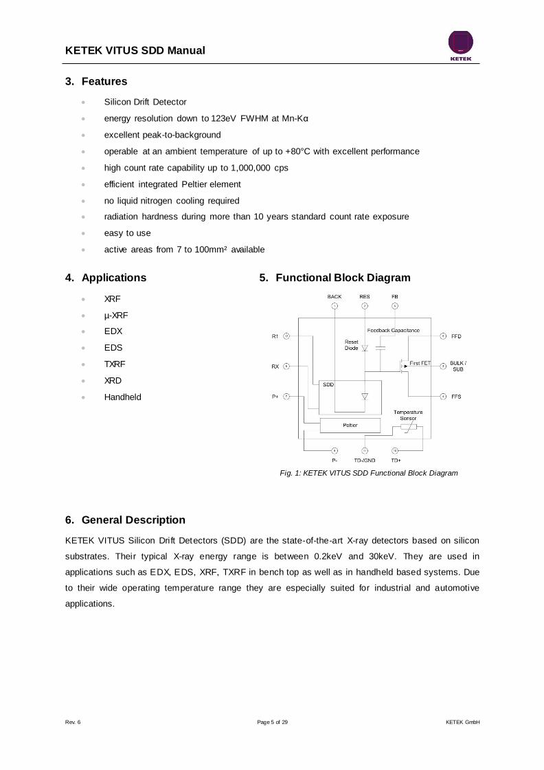
5. Functional Block Diagram
Fig. 1: KETEK VITUS SDD Functional Block Diagram
6. General Description
KETEK VITUS Silicon Drift Detectors (SDD) are the state-of-the-art X-ray detectors based on silicon
substrates. Their typical X-ray energy range is between 0.2keV and 30keV. They are used in
applications such as EDX, EDS, XRF, TXRF in bench top as well as in handheld based systems. Due
to their wide operating temperature range they are especially suited for industrial and automotive
applications.
KETEK VITUS SDD Manual
Rev. 6 Page 6 of 29 KETEK GmbH
7. Safety
It is strongly recommended to read this user manual carefully and completely before installing or
activating the SDD. Please keep this user manual always with the system for that any operator can get
this important information. In case of resale – even when second hand – or in case of scrapping at the
end of lifetime this manual has to be given along with the system. Please handle the attached
documents “Beryllium Material Data Sheet” and “Statement of contamination…” the same way.
WARNING!
The detector contains a thin, fragile Be window. If this window is damaged, the detector will be destroyed and cannot be repaired.
Be windows damaged due to improper handling are not covered under warranty.
This product uses – a very small amount - of toxic beryllium material at the inner side of the detector foil. Beryllium is preferred as an entrance window coating because i t
provides a light-tight seal and, further, does not introduce spurious peaks in the measured spectrum. In normal operation there is no danger to get in contact with any toxic materials. If the SDD window was destroyed by accident, follow our safety
instructions.
Scrapping at end of lifetime has to be done according to the (local) legal requirements. Make the “Beryllium Material Data Sheet” available to your waste disposal contractor. Do not scrap the SDD to your domestic waste.
Due to the very thin window foil you should take care neither to touch it with fingers nor
to bring other things or materials under test too near to it. Keep away excessive dust particle streams from the SDD window.
Excessive electrostatic discharge might destroy the window. Take care ESD is well bled
off in your application.
Some of the SDD types are evacuated. A damaged entrance window may implode scattering small beryllium particles in the immediate vicinity of the SDD. In this case, rigorously clean the SDD and its surrounding area following all the precautions
mentioned in the “Beryllium Material Safety Data Sheet”.
Always keep the SDD protection cap with the system, even if fixed mounted. It’s necessary for cleaning, service and shipping to be able to protect the beryllium window.
CAUTION!
High voltages need to be applied to the detector for use. To prevent electrical shock, do not touch the detector.
Do not drop or cause mechanical shock to the detector. Components inside the detector
are mechanically fragile and may be damaged if the unit is dropped. Avoid temperature shocks. If the detector is out of allowed temperature range, make
sure to acclimate slowly. Avoid air pressure shocks. Especially in evacuated applications take care to ventilate
slowly. Let the protection cap be mounted at the SDD as long as the system isn’t mounted in its
end application. Your end application has to be designed that way to make unexpected, damaging contact with the SDD window impossible. Make sure your samples under test might never touch the SDD window.
Do not remove the protective cap from the detector until data is to be taken. The detector
window is made from thin beryllium which is extremely brittle and can shatter very easily. Do not have any object come in contact with the window. Do not touch the detector because the oil from the fingers will cause it to oxidize. Use gloves. The window cannot
be repaired. If the window is damaged the detector assembly must be replaced. Be windows damaged due to improper handling will not be covered under warranty. Keep the protective cover nearby at all times and cover the detector when the instrument is not
in use.
KETEK VITUS SDD Manual
Rev. 6 Page 7 of 29 KETEK GmbH
Radiation damage to the detector will occur i f it is exposed to a high flux environment.
Synchrotron Radiation Beams should be modified with attenuators before they are allowed to strike the detector or the fluorescence target. Damage to the detector will be
permanent if the flux from an X-Ray Tube, a strong nuclear radiation source, or an accelerator is not attenuated.
No user serviceable parts inside the units. Refer servicing to KETEK GmbH. To prevent electrical shock, do not remove covers.
Keep the device dry and clean!
Warranty
KETEK GmbH warrants to the original purchaser this instrument to be free from defects in materials
and workmanship for a period of one year from shipment. KETEK GmbH will, without charge, repair or
replace (at its option) a defective instrument upon return to the factory. This warranty does not apply in
the event of misuse or abuse of the instrument or unauthorized alterations or repair. KETEK GmbH
shall not be liable for any consequential damages, including without limitation, damages resulting from
the loss of use due to failure of this instrument. All products returned under the warranty must be
shipped prepaid to the factory with documentation describing the problem and the circumstances
under which it was observed. Additionally the statement of contamination must be filled out completely
and returned with the product. KETEK must be notified prior to return shipment. The instrument will be
evaluated, repaired or replaced, and promptly returned if the warranty claims are substantiated. A
nominal fee will be charged for unsubstantiated claims. Please include the model and serial number i n
all correspondence with KETEK.
Care Instructions
Do not clean the SDD under any circumstances. Do not use any alcoholic, acid or rubbing cleaning
agents.
8. General Restrictions and Recommendations
- do not use detector without heat sink connection. Overheating will destroy the module
- do not solder the pins or any other part of the detector module
- avoid touching the detector module
- use gloves to avoid corrosion
- avoid touching the entrance window of the detector module. It contains hazardous materials
KETEK VITUS SDD Manual
Rev. 6 Page 8 of 29 KETEK GmbH
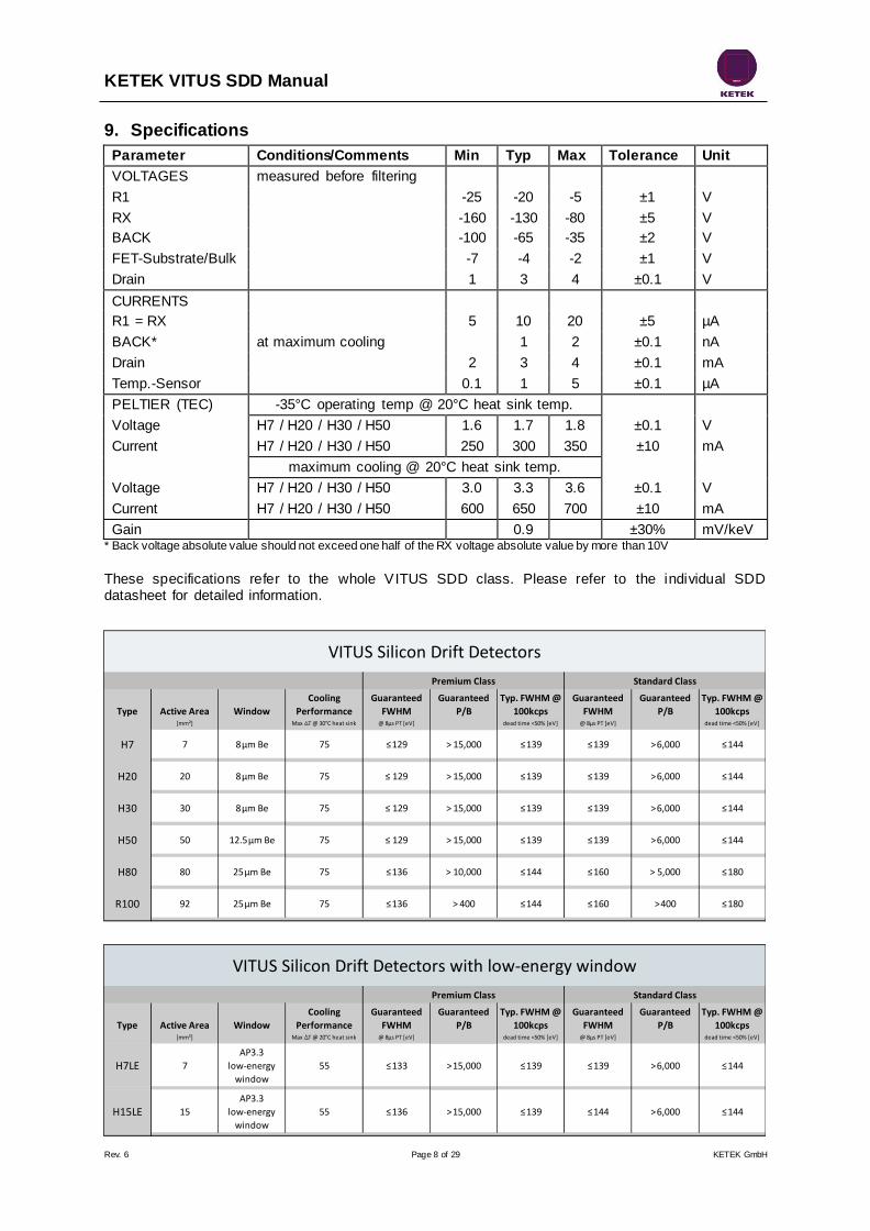
9. Specifications
Parameter Conditions/Comments Min Typ Max Tolerance Unit
VOLTAGES measured before filtering
R1 -25 -20 -5 ±1 V
RX -160 -130 -80 ±5 V
BACK -100 -65 -35 ±2 V
FET-Substrate/Bulk -7 -4 -2 ±1 V
Drain 1 3 4 ±0.1 V
CURRENTS
R1 = RX 5 10 20 ±5 µA
BACK* at maximum cooling 1 2 ±0.1 nA
Drain 2 3 4 ±0.1 mA
Temp.-Sensor 0.1 1 5 ±0.1 µA
PELTIER (TEC) -35°C operating temp @ 20°C heat sink temp.
Voltage H7 / H20 / H30 / H50 1.6 1.7 1.8 ±0.1 V
Current H7 / H20 / H30 / H50 250 300 350 ±10 mA
maximum cooling @ 20°C heat sink temp.
Voltage H7 / H20 / H30 / H50 3.0 3.3 3.6 ±0.1 V
Current H7 / H20 / H30 / H50 600 650 700 ±10 mA
Gain 0.9 ±30% mV/keV * Back voltage absolute value should not exceed one half of the RX voltage absolute value by more than 10V
These specifications refer to the whole VITUS SDD class. Please refer to the individual SDD datasheet for detailed information.
Type Active Area Window
Cooling
Performance
Guaranteed
FWHM
Guaranteed
P/B
Typ. FWHM @
100kcps
Guaranteed
FWHM
Guaranteed
P/B
Typ. FWHM @
100kcps[mm²] Max T @ 30°C heat sink @ 8µs PT [eV] dead time <50% [eV] @ 8µs PT [eV] dead time <50% [eV]
H7 7 8 µm Be 75 ≤ 129 > 15,000 ≤ 139 ≤ 139 > 6,000 ≤ 144
H20 20 8 µm Be 75 ≤ 129 > 15,000 ≤ 139 ≤ 139 > 6,000 ≤ 144
H30 30 8 µm Be 75 ≤ 129 > 15,000 ≤ 139 ≤ 139 > 6,000 ≤ 144
H50 50 12.5 µm Be 75 ≤ 129 > 15,000 ≤ 139 ≤ 139 > 6,000 ≤ 144
H80 80 25 µm Be 75 ≤ 136 > 10,000 ≤ 144 ≤ 160 > 5,000 ≤ 180
R100 92 25 µm Be 75 ≤ 136 > 400 ≤ 144 ≤ 160 > 400 ≤ 180
Type Active Area Window
Cooling
Performance
Guaranteed
FWHM
Guaranteed
P/B
Typ. FWHM @
100kcps
Guaranteed
FWHM
Guaranteed
P/B
Typ. FWHM @
100kcps[mm²] Max T @ 20°C heat sink @ 8µs PT [eV] dead time <50% [eV] @ 8µs PT [eV] dead time <50% [eV]
H7LE 7
AP3.3
low-energy
window
55 ≤ 133 > 15,000 ≤ 139 ≤ 139 > 6,000 ≤ 144
H15LE 15
AP3.3
low-energy
window
55 ≤ 136 > 15,000 ≤ 139 ≤ 144 > 6,000 ≤ 144
Premium Class Standard Class
VITUS Silicon Drift Detectors
VITUS Silicon Drift Detectors with low-energy window
Premium Class Standard Class
KETEK VITUS SDD Manual
Rev. 6 Page 9 of 29 KETEK GmbH
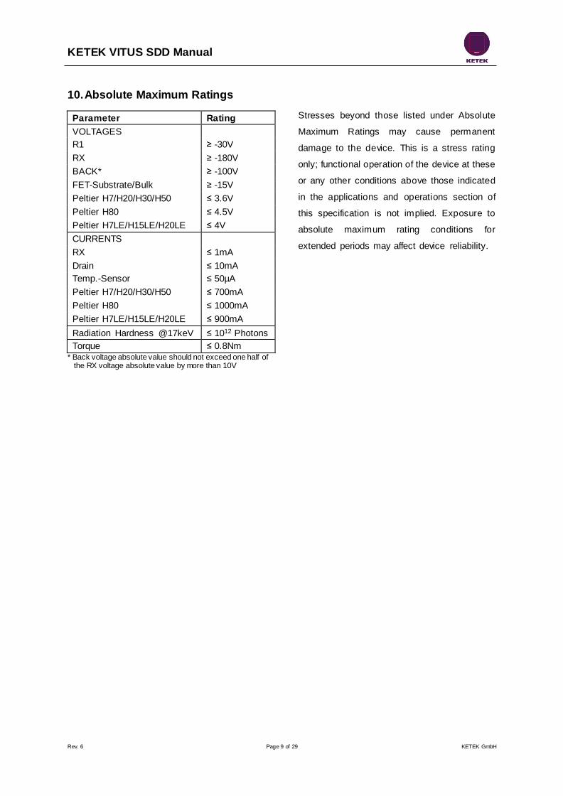
10. Absolute Maximum Ratings
Parameter Rating
VOLTAGES
R1 ≥ -30V
RX ≥ -180V
BACK* ≥ -100V
FET-Substrate/Bulk ≥ -15V
Peltier H7/H20/H30/H50 ≤ 3.6V
Peltier H80 ≤ 4.5V
Peltier H7LE/H15LE/H20LE ≤ 4V
CURRENTS
RX ≤ 1mA
Drain ≤ 10mA
Temp.-Sensor ≤ 50µA
Peltier H7/H20/H30/H50 ≤ 700mA
Peltier H80 ≤ 1000mA
Peltier H7LE/H15LE/H20LE ≤ 900mA
Radiation Hardness @17keV ≤ 1012 Photons
Torque ≤ 0.8Nm
Stresses beyond those listed under Absolute
Maximum Ratings may cause permanent
damage to the device. This is a stress rating
only; functional operation of the device at these
or any other conditions above those indicated
in the applications and operations section of
this specification is not implied. Exposure to
absolute maximum rating conditions for
extended periods may affect device reliability.
* Back voltage absolute value should not exceed one half of the RX voltage absolute value by more than 10V
KETEK VITUS SDD Manual
Rev. 6 Page 10 of 29 KETEK GmbH
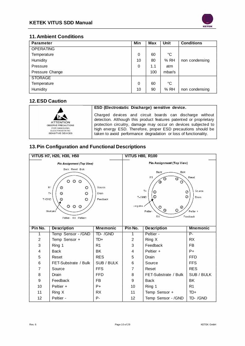
11. Ambient Conditions
Parameter Min Max Unit Conditions
OPERATING
Temperature 0 60 °C
Humidity 10 80 % RH non condensing
Pressure 0 1.1 atm
Pressure Change 100 mbar/s
STORAGE
Temperature 0 60 °C
Humidity 10 90 % RH non condensing
12. ESD Caution
ESD (Electrostatic Discharge) sensitive device.
Charged devices and circuit boards can discharge without detection. Although this product features patented or proprietary
protection circuitry, damage may occur on devices subjected to high energy ESD. Therefore, proper ESD precautions should be taken to avoid performance degradation or loss of functionality.
13. Pin Configuration and Functional Descriptions
VITUS H7, H20, H30, H50 VITUS H80, R100
Pin No. Description Mnemonic Pin No. Description Mnemonic
1 Temp Sensor - /GND TD- /GND 1 Peltier - P-
2 Temp Sensor + TD+ 2 Ring X RX
3 Ring 1 R1 3 Feedback FB
4 Back BK 4 Peltier + P+
5 Reset RES 5 Drain FFD
6 FET-Substrate / Bulk SUB / BULK 6 Source FFS
7 Source FFS 7 Reset RES
8 Drain FFD 8 FET-Substrate / Bulk SUB / BULK
9 Feedback FB 9 Back BK
10 Peltier + P+ 10 Ring 1 R1
11 Ring X RX 11 Temp Sensor + TD+
12 Peltier - P- 12 Temp Sensor - /GND TD- /GND
KETEK VITUS SDD Manual
Rev. 6 Page 11 of 29 KETEK GmbH
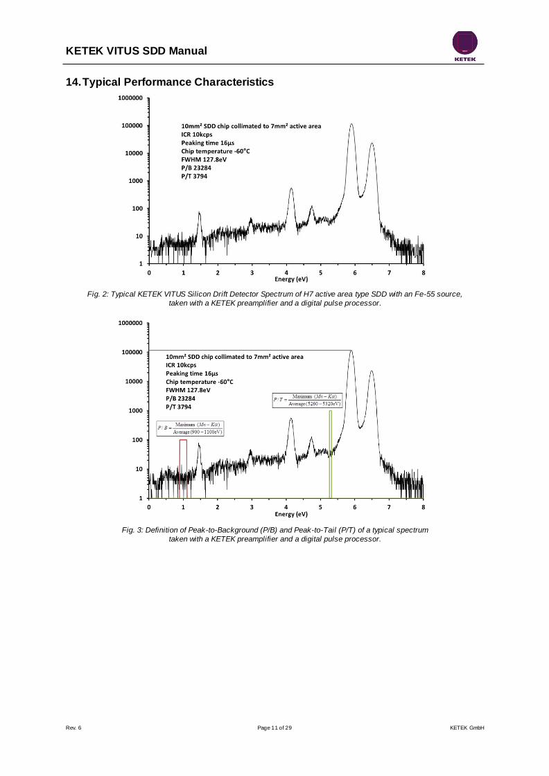
14. Typical Performance Characteristics
Fig. 2: Typical KETEK VITUS Silicon Drift Detector Spectrum of H7 active area type SDD with an Fe-55 source,
taken with a KETEK preamplifier and a digital pulse processor.
Fig. 3: Definition of Peak-to-Background (P/B) and Peak-to-Tail (P/T) of a typical spectrum
taken with a KETEK preamplifier and a digital pulse processor.
KETEK VITUS SDD Manual
Rev. 6 Page 12 of 29 KETEK GmbH
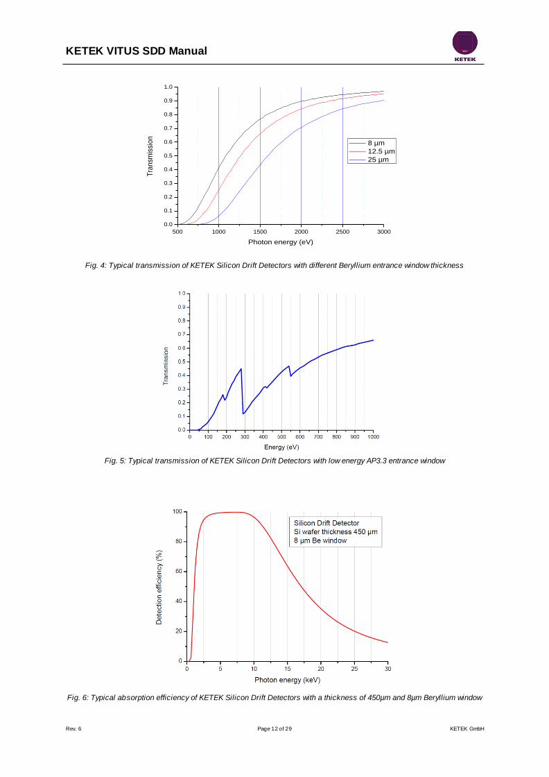
Fig. 4: Typical transmission of KETEK Silicon Drift Detectors with different Beryllium entrance window thickness
Fig. 5: Typical transmission of KETEK Silicon Drift Detectors with low energy AP3.3 entrance window
Fig. 6: Typical absorption efficiency of KETEK Silicon Drift Detectors with a thickness of 450µm and 8µm Beryllium window
500 1000 1500 2000 2500 3000
0.0
0.1
0.2
0.3
0.4
0.5
0.6
0.7
0.8
0.9
1.0
Tra
nsm
issi
on
Photon energy (eV)
8 µm
12.5 µm
25 µm
KETEK VITUS SDD Manual
Rev. 6 Page 13 of 29 KETEK GmbH
20 25 30 35 40 45 50 55 60 65 70 75 80
-40
-35
-30
-25
-20
-15
-10
-5
0
5
10
SD
D C
hip
Te
mp
era
ture
[°C
]
Heat Sink Temperature [°C]
e.g. stable 0°C chip temperature
up to +70°C heat sink temperature
e.g. stable -10°C chip temperature
up to +55°C heat sink temperature
e.g. stable -20°C chip temperature
up to +40°C heat sink temp.
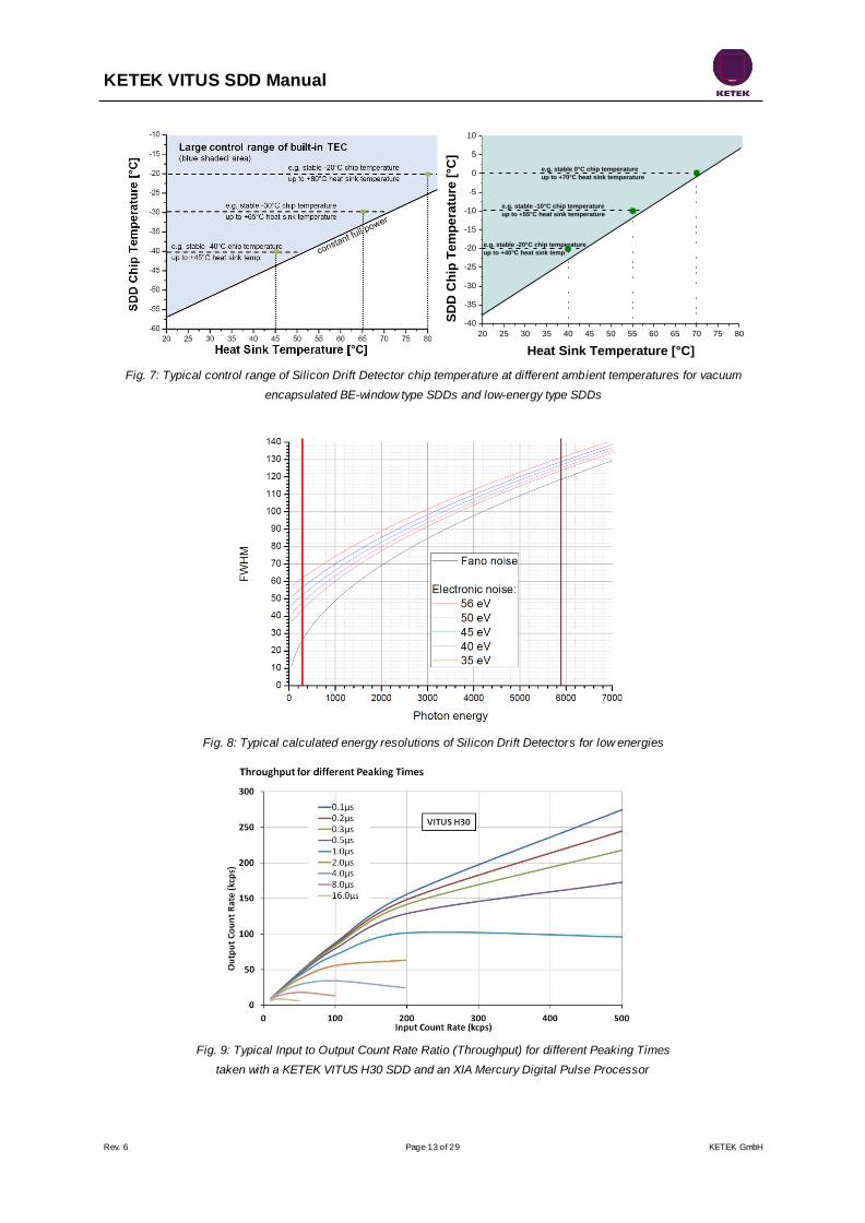
Fig. 7: Typical control range of Silicon Drift Detector chip temperature at different ambient temperatures for vacuum
encapsulated BE-window type SDDs and low-energy type SDDs
Fig. 8: Typical calculated energy resolutions of Silicon Drift Detectors for low energies
Fig. 9: Typical Input to Output Count Rate Ratio (Throughput) for different Peaking Times
taken with a KETEK VITUS H30 SDD and an XIA Mercury Digital Pulse Processor
KETEK VITUS SDD Manual
Rev. 6 Page 14 of 29 KETEK GmbH
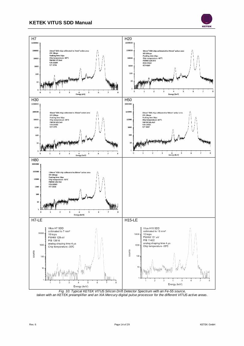
H7
H20
H30
H50
H80
H7-LE
H15-LE
Fig. 10: Typical KETEK VITUS Silicon Drift Detector Spectrum with an Fe-55 source, taken with an KETEK preamplifier and an XIA Mercury digital pulse processor for the different VITUS active areas.
KETEK VITUS SDD Manual
Rev. 6 Page 15 of 29 KETEK GmbH
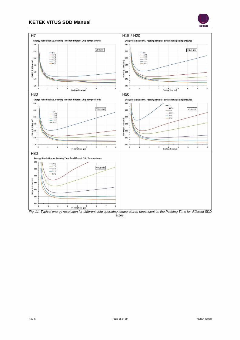
H7
H15 / H20
H30
H50
H80
Fig. 11: Typical energy resolution for different chip operating temperatures dependent on the Peaking Time for different SDD sizes.
KETEK VITUS SDD Manual
Rev. 6 Page 16 of 29 KETEK GmbH
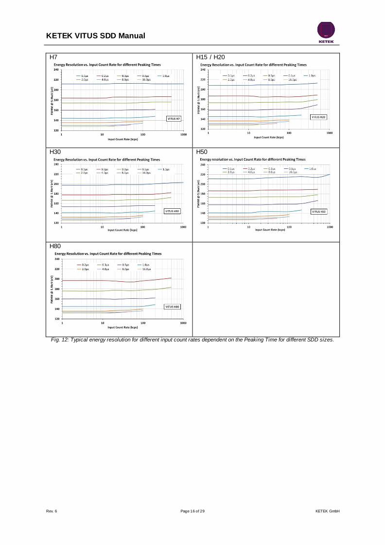
H7
H15 / H20
H30
H50
H80
Fig. 12: Typical energy resolution for different input count rates dependent on the Peaking Time for different SDD sizes.
KETEK VITUS SDD Manual
Rev. 6 Page 17 of 29 KETEK GmbH
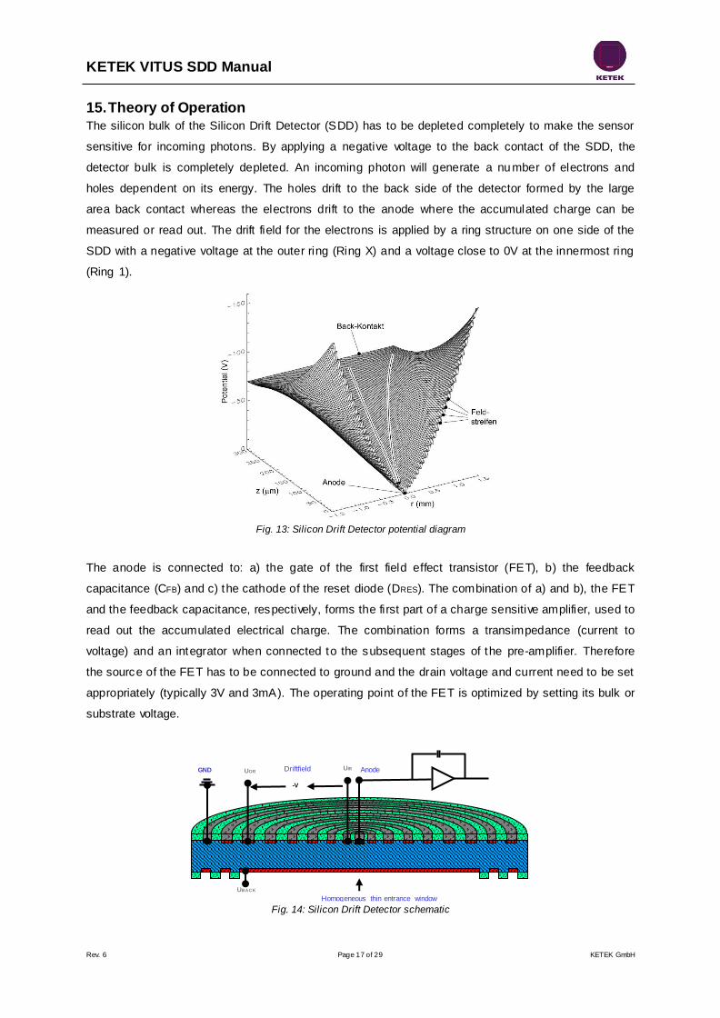
15. Theory of Operation
The silicon bulk of the Silicon Drift Detector (SDD) has to be depleted completely to make the sensor
sensitive for incoming photons. By applying a negative voltage to the back contact of the SDD, the
detector bulk is completely depleted. An incoming photon will generate a number of electrons and
holes dependent on its energy. The holes drift to the back side of the detector formed by the large
area back contact whereas the electrons drift to the anode where the accumulated charge can be
measured or read out. The drift field for the electrons is applied by a ring structure on one side of the
SDD with a negative voltage at the outer ring (Ring X) and a voltage close to 0V at the innermost ring
(Ring 1).
Fig. 13: Silicon Drift Detector potential diagram
The anode is connected to: a) the gate of the first field effect transistor (FET), b) the feedback
capacitance (CFB) and c) the cathode of the reset diode (DRES). The combination of a) and b), the FET
and the feedback capacitance, respectively, forms the first part of a charge sensitive amplifier, used to
read out the accumulated electrical charge. The combination forms a transimpedance (current to
voltage) and an integrator when connected to the subsequent stages of the pre-amplifier. Therefore
the source of the FET has to be connected to ground and the drain voltage and current need to be set
appropriately (typically 3V and 3mA). The operating point of the FET is optimized by setting its bulk or
substrate voltage.
Fig. 14: Silicon Drift Detector schematic
GND UOR UIR
UBACK
Homogeneous thin entrance window
-V
Driftfield Anode
KETEK VITUS SDD Manual
Rev. 6 Page 18 of 29 KETEK GmbH
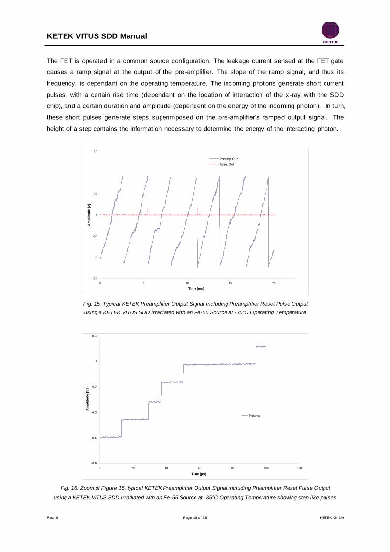
The FET is operated in a common source configuration. The leakage current sensed at the FET gate
causes a ramp signal at the output of the pre-amplifier. The slope of the ramp signal, and thus its
frequency, is dependant on the operating temperature. The incoming photons generate short current
pulses, with a certain rise time (dependant on the location of interaction of the x -ray with the SDD
chip), and a certain duration and amplitude (dependent on the energy of the incoming photon). In turn,
these short pulses generate steps superimposed on the pre-amplifier’s ramped output signal. The
height of a step contains the information necessary to determine the energy of the interacting photon.
Fig. 15: Typical KETEK Preamplifier Output Signal including Preamplifier Reset Pulse Output
using a KETEK VITUS SDD irradiated with an Fe-55 Source at -35°C Operating Temperature
Fig. 16: Zoom of Figure 15, typical KETEK Preamplifier Output Signal including Preamplifier Reset Pulse Output
using a KETEK VITUS SDD irradiated with an Fe-55 Source at -35°C Operating Temperature showing step like pulses
-1,5
-1
-0,5
0
0,5
1
1,5
0 5 10 15 20
Time [ms]
Am
pli
tud
e [
V]
Preamp Out
Reset Out
-0,16
-0,12
-0,08
-0,04
0
0,04
0 20 40 60 80 100 120
Time [µs]
Am
pli
tud
e [
V]
PreampOut
KETEK VITUS SDD Manual
Rev. 6 Page 19 of 29 KETEK GmbH
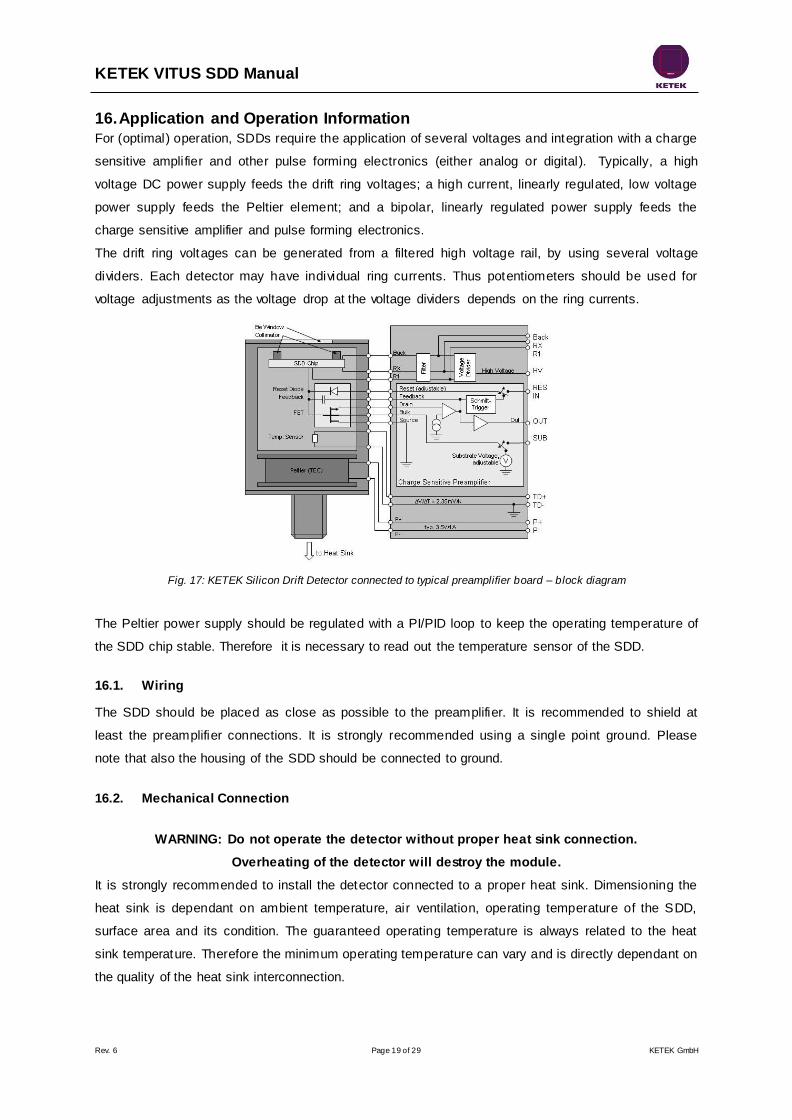
16. Application and Operation Information
For (optimal) operation, SDDs require the application of several voltages and integration with a charge
sensitive amplifier and other pulse forming electronics (either analog or digital). Typically, a high
voltage DC power supply feeds the drift ring voltages; a high current, linearly regulated, low voltage
power supply feeds the Peltier element; and a bipolar, linearly regulated power supply feeds the
charge sensitive amplifier and pulse forming electronics.
The drift ring voltages can be generated from a filtered high voltage rail, by using several voltage
dividers. Each detector may have individual ring currents. Thus potentiometers should be used for
voltage adjustments as the voltage drop at the voltage dividers depends on the ring currents.
Fig. 17: KETEK Silicon Drift Detector connected to typical preamplifier board – block diagram
The Peltier power supply should be regulated with a PI/PID loop to keep the operating temperature of
the SDD chip stable. Therefore it is necessary to read out the temperature sensor of the SDD.
16.1. Wiring
The SDD should be placed as close as possible to the preamplifier. It is recommended to shield at
least the preamplifier connections. It is strongly recommended using a single point ground. Please
note that also the housing of the SDD should be connected to ground.
16.2. Mechanical Connection
WARNING: Do not operate the detector without proper heat sink connection.
Overheating of the detector will destroy the module.
It is strongly recommended to install the detector connected to a proper heat sink. Dimensioning the
heat sink is dependant on ambient temperature, air ventilation, operating temperature of the SDD,
surface area and its condition. The guaranteed operating temperature is always related to the heat
sink temperature. Therefore the minimum operating temperature can vary and is directly dependant on
the quality of the heat sink interconnection.
KETEK VITUS SDD Manual
Rev. 6 Page 20 of 29 KETEK GmbH
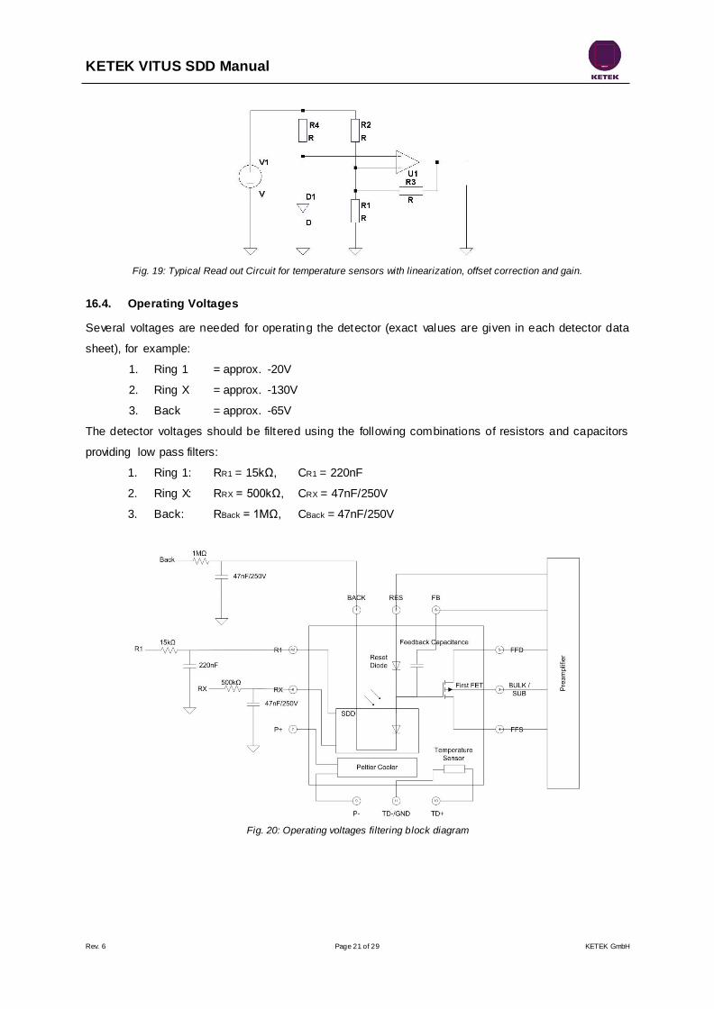
16.3. Read out Circuit for Temperature Sensor
a) Temperature Diode:
Using a diode as temperature sensor leads to a linear relationship between the measured voltage and
sensor temperature. The line’s slope depends on the diode bias current . For the recommended 1µA,
the slope is 2.35mV/K. It is recommended to apply a constant current.
b) Thermistor (NTC resistor):
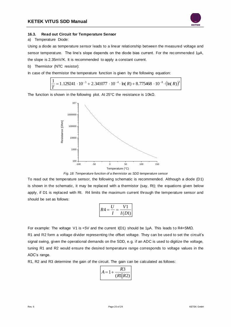
In case of the thermistor the temperature function is given by the following equation:
3843 )ln(10775468.8)ln(10341077.210129241.11
RRT
The function is shown in the following plot. At 25°C the resistance is 10kΩ.
Fig. 18: Temperature function of a thermistor as SDD temperature sensor
To read out the temperature sensor, the following schematic is recommended. Although a diode (D1)
is shown in the schematic, it may be replaced with a thermistor (say, Rt); the equations given below
apply, if D1 is replaced with Rt. R4 limits the maximum current through the temperature sensor and
should be set as follows:
)1(
14
DI
V
I
UR
For example: The voltage V1 is +5V and the current I(D1) should be 1µA. This leads to R4=5MΩ.
R1 and R2 form a voltage divider representing the offset voltage. They can be used to set the circuit’s
signal swing, given the operational demands on the SDD, e.g. i f an ADC is used to digitize the voltage,
tuning R1 and R2 would ensure the desired temperature range corresponds to voltage values in the
ADC’s range.
R1, R2 and R3 determine the gain of the circuit. The gain can be calculated as follows:
)21(
31
RR
RA
-100 -50 0 50 100 150
100
1000
10000
100000
1000000
1E7
Re
sis
tan
ce
[O
hm
]
Temperature (°C)
KETEK VITUS SDD Manual
Rev. 6 Page 21 of 29 KETEK GmbH
Fig. 19: Typical Read out Circuit for temperature sensors with linearization, offset correction and gain.
16.4. Operating Voltages
Several voltages are needed for operating the detector (exact values are given in each detector data
sheet), for example:
1. Ring 1 = approx. -20V
2. Ring X = approx. -130V
3. Back = approx. -65V
The detector voltages should be filtered using the following combinations of resistors and capacitors
providing low pass filters:
1. Ring 1: RR1 = 15kΩ, CR1 = 220nF
2. Ring X: RRX = 500kΩ, CRX = 47nF/250V
3. Back: RBack = 1MΩ, CBack = 47nF/250V
Fig. 20: Operating voltages filtering block diagram
KETEK VITUS SDD Manual
Rev. 6 Page 22 of 29 KETEK GmbH
Before switching on the system, the output-signal of the preamplifier and the shaped signal should be
connected to an oscilloscope.
The preamplifier operating voltage must be switched on first.
The detector voltages should be switched on in the following order:
R1 – RX – Back
The voltages to be applied must be set according to the detector datasheet . Typical currents flowing
are several μA through Ring 1 and Ring X (voltage divider) and approx. 1nA for the back contact if the
back voltage is applied. R1 and RX currents should be equal!
After switching on the detector voltages the signal of the preamplifier should show a ramp. The ramp
period depends on the chip temperature. At -35°C the ramp period should be in the range of several
microseconds.
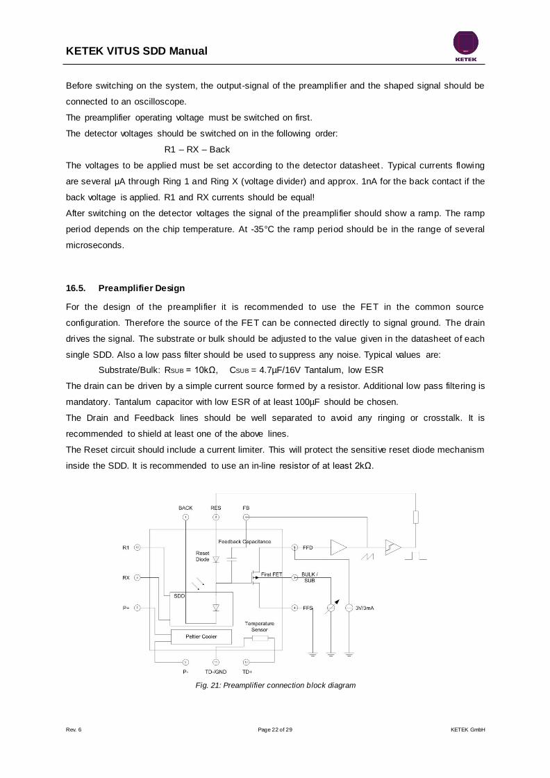
16.5. Preamplifier Design
For the design of the preamplifier it is recommended to use the FET in the common source
configuration. Therefore the source of the FET can be connected directly to signal ground. The drain
drives the signal. The substrate or bulk should be adjusted to the value given in the datasheet of each
single SDD. Also a low pass filter should be used to suppress any noise. Typical values are:
Substrate/Bulk: RSUB = 10kΩ, CSUB = 4.7µF/16V Tantalum, low ESR
The drain can be driven by a simple current source formed by a resistor. Additional low pass filtering is
mandatory. Tantalum capacitor with low ESR of at least 100µF should be chosen.
The Drain and Feedback lines should be well separated to avoid any ringing or crosstalk. It is
recommended to shield at least one of the above lines.
The Reset circuit should include a current limiter. This will protect the sensitive reset diode mechanism
inside the SDD. It is recommended to use an in-line resistor of at least 2kΩ.
Fig. 21: Preamplifier connection block diagram
KETEK VITUS SDD Manual
Rev. 6 Page 23 of 29 KETEK GmbH
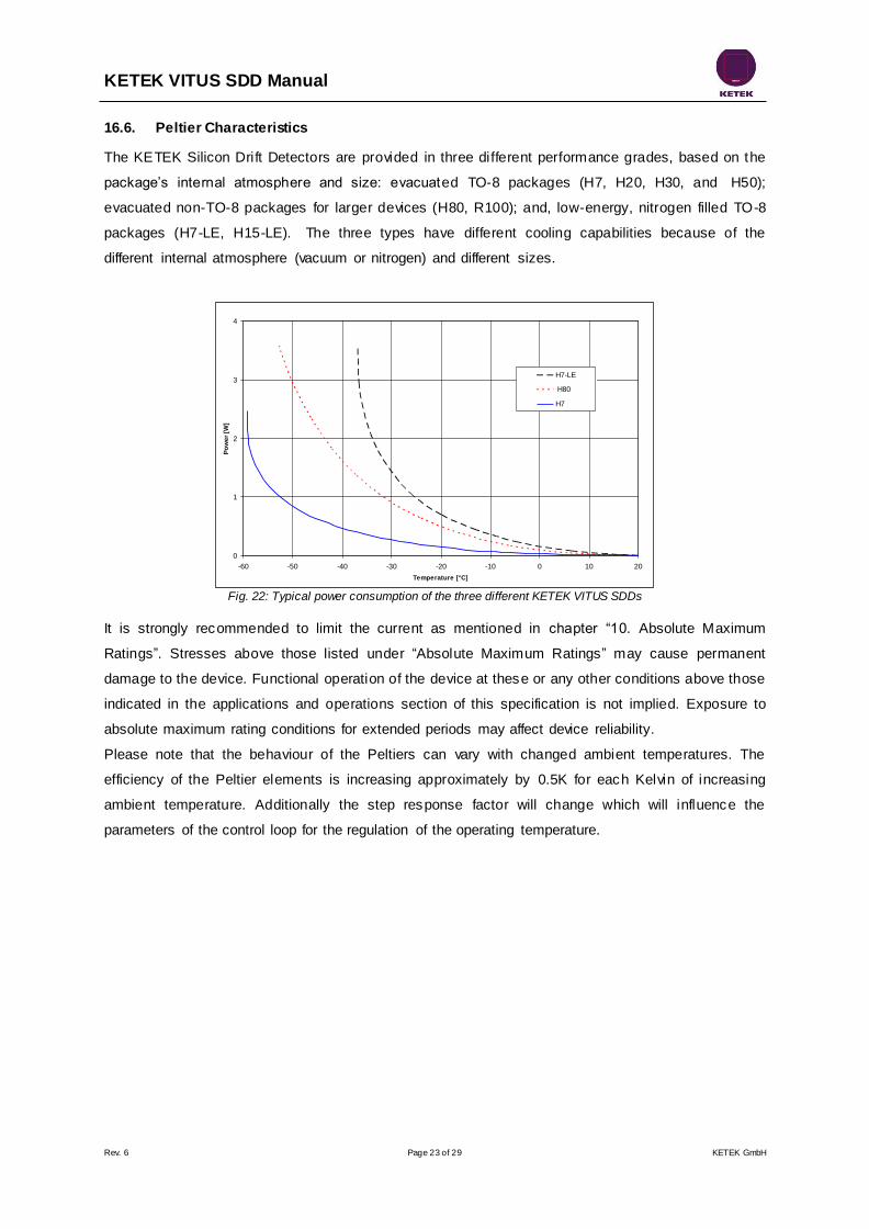
16.6. Peltier Characteristics
The KETEK Silicon Drift Detectors are provided in three different performance grades, based on the
package’s internal atmosphere and size: evacuated TO-8 packages (H7, H20, H30, and H50);
evacuated non-TO-8 packages for larger devices (H80, R100); and, low-energy, nitrogen filled TO-8
packages (H7-LE, H15-LE). The three types have different cooling capabilities because of the
different internal atmosphere (vacuum or nitrogen) and different sizes.
Fig. 22: Typical power consumption of the three different KETEK VITUS SDDs
It is strongly recommended to limit the current as mentioned in chapter “10. Absolute Maximum
Ratings”. Stresses above those listed under “Absolute Maximum Ratings” may cause permanent
damage to the device. Functional operation of the device at these or any other conditions above those
indicated in the applications and operations section of this specification is not implied. Exposure to
absolute maximum rating conditions for extended periods may affect device reliability.
Please note that the behaviour of the Peltiers can vary with changed ambient temperatures. The
efficiency of the Peltier elements is increasing approximately by 0.5K for each Kelvin of increasing
ambient temperature. Additionally the step response factor will change which will influence the
parameters of the control loop for the regulation of the operating temperature.
0
1
2
3
4
-60 -50 -40 -30 -20 -10 0 10 20
Temperature [°C]
Po
we
r [W
]
H7-LE
H80
H7
KETEK VITUS SDD Manual
Rev. 6 Page 24 of 29 KETEK GmbH
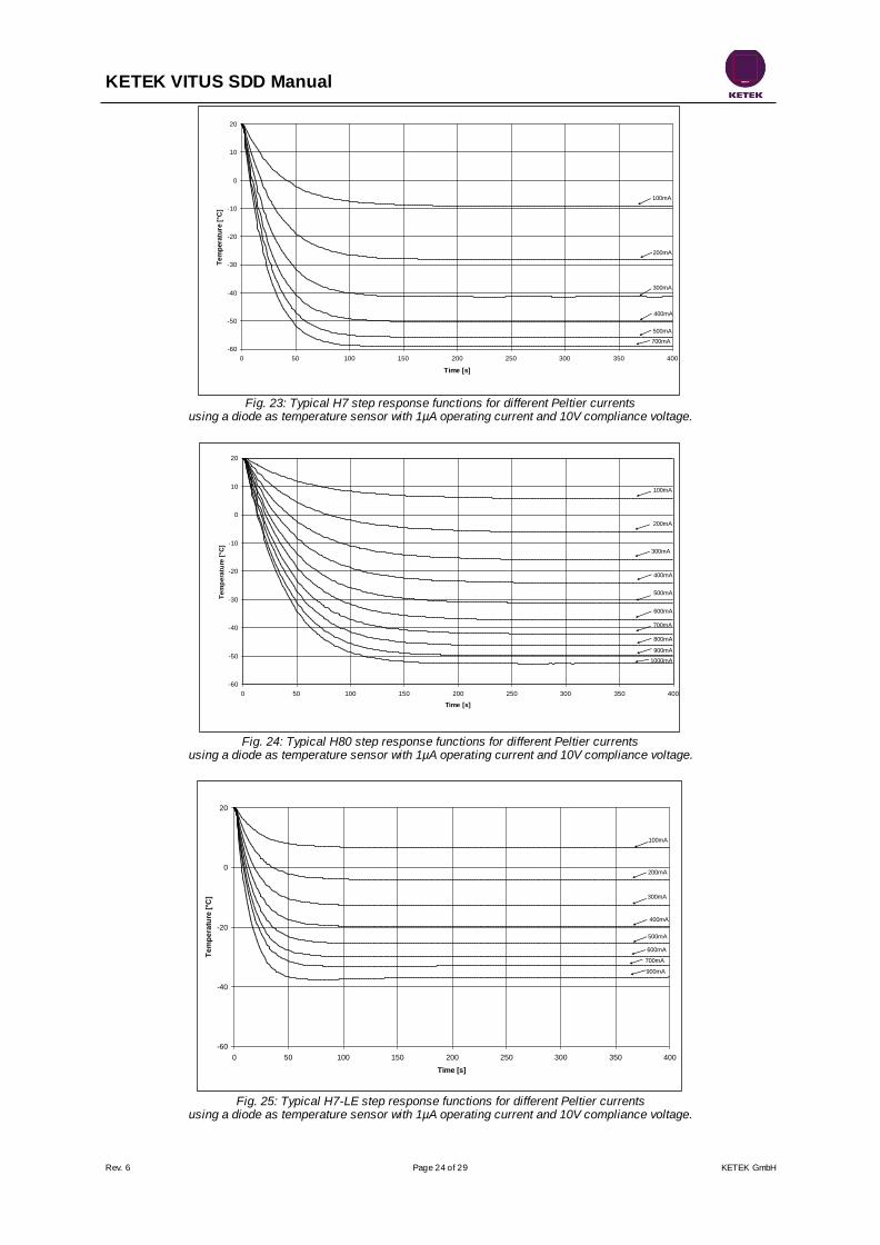
Fig. 23: Typical H7 step response functions for different Peltier currents
using a diode as temperature sensor with 1µA operating current and 10V compliance voltage.
Fig. 24: Typical H80 step response functions for different Peltier currents
using a diode as temperature sensor with 1µA operating current and 10V compliance voltage.
Fig. 25: Typical H7-LE step response functions for different Peltier currents
using a diode as temperature sensor with 1µA operating current and 10V compliance voltage.
-60
-50
-40
-30
-20
-10
0
10
20
0 50 100 150 200 250 300 350 400
Time [s]
Tem
pera
ture
[°C
]
100mA
200mA
300mA
400mA
500mA
700mA
-60
-50
-40
-30
-20
-10
0
10
20
0 50 100 150 200 250 300 350 400
Time [s]
Te
mp
era
ture
[°C
]
100mA
200mA
300mA
400mA
500mA
600mA
700mA
800mA
1000mA
900mA
-60
-40
-20
0
20
0 50 100 150 200 250 300 350 400
Time [s]
Te
mp
era
ture
[°C
]
100mA
200mA
300mA
400mA
500mA
600mA
700mA
900mA
KETEK VITUS SDD Manual
Rev. 6 Page 25 of 29 KETEK GmbH
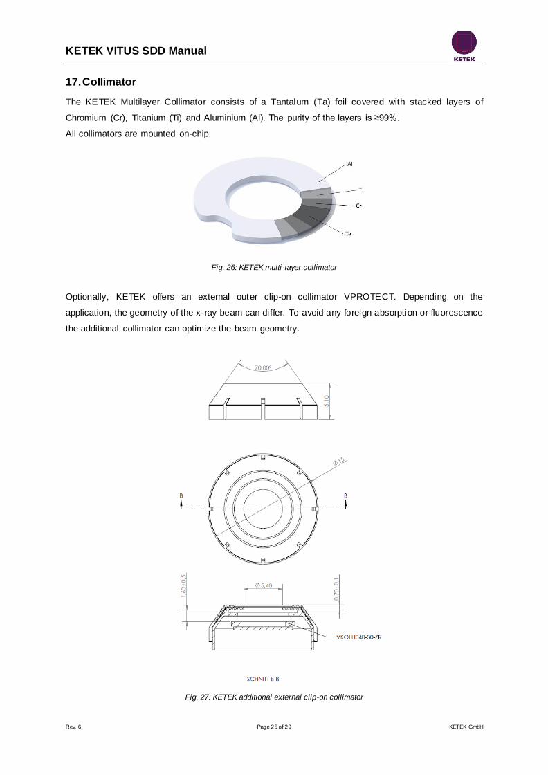
17. Collimator
The KETEK Multilayer Collimator consists of a Tantalum (Ta) foil covered with stacked layers of
Chromium (Cr), Titanium (Ti) and Aluminium (Al). The purity of the layers is ≥99%.
All collimators are mounted on-chip.
Fig. 26: KETEK multi-layer collimator
Optionally, KETEK offers an external outer clip-on collimator VPROTECT. Depending on the
application, the geometry of the x-ray beam can differ. To avoid any foreign absorption or fluorescence
the additional collimator can optimize the beam geometry.
Fig. 27: KETEK additional external clip-on collimator
KETEK VITUS SDD Manual
Rev. 6 Page 26 of 29 KETEK GmbH
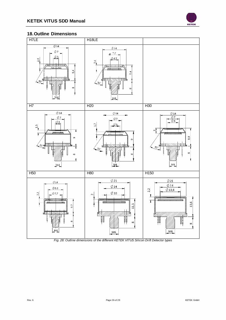
18. Outline Dimensions
H7LE H18LE
H7 H20 H30
H50 H80 H150
Fig. 28: Outline dimensions of the different KETEK VITUS Silicon Drift Detector types
Ø
KETEK VITUS SDD Manual
Rev. 6 Page 27 of 29 KETEK GmbH
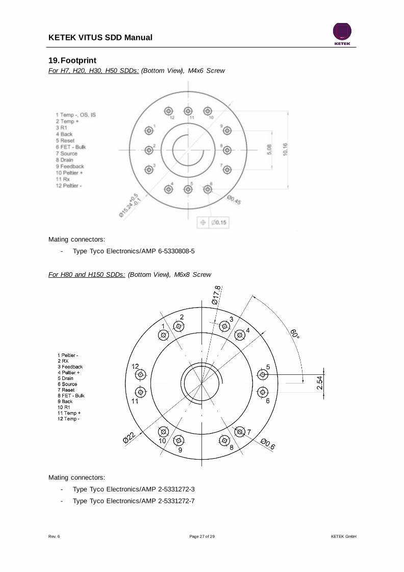
19. Footprint
For H7, H20, H30, H50 SDDs: (Bottom View), M4x6 Screw
Mating connectors:
- Type Tyco Electronics/AMP 6-5330808-5
For H80 and H150 SDDs: (Bottom View), M6x8 Screw
Mating connectors:
- Type Tyco Electronics/AMP 2-5331272-3
- Type Tyco Electronics/AMP 2-5331272-7
KETEK VITUS SDD Manual
Rev. 6 Page 28 of 29 KETEK GmbH
20. Ordering Guide
V 5 F 2 O - -
Pro
duct
VIT
US
Chip
thic
kness
450µ
m
FE
T
Peltie
r
Tem
p.
Sensor
Chip
entr
ance
win
dow
Active a
rea
Colli
mato
r
mate
rial
Cap
Win
dow
Encapsula
tion
Example:
V5F2T0-H30-ML8BEV: VITUS 450µm SDD Chip with low capacitance FET and a Thermistor as
temperature sensor, active area of 30mm² with high peak-to-background ratio, multilayer collimator in
a bevelled cap with a Be window sealed under vacuum.
21. Optional
Optional available are different KETEK products in combination with the VITUS Silicon Drift Detector:
- KETEK Preamplifier: High performance stand-alone preamplifier for SDD applications
- KETEK VICO: VITUS Components, -PA: Preamplifier, -TC: TEC/Peltier Controller, -HV: High
Voltage Power Supply, -DP: Digital Pulse Processor, -EV: Evaluation Board
- KETEK VIAMP: VITUS SDD in combination with preamplifier
- KETEK AXAS: Analytical X-ray Acquisition System
- KETEK VPROTECT: external collimator
For detailed information please contact KETEK Sales and Marketing Office.
KETEK VITUS SDD Manual
Rev. 6 Page 29 of 29 KETEK GmbH
22. Contact
KETEK Headquarter Sales Office
KETEK GmbH
Hofer Str. 3
81737 München
Email [email protected]
Phone +49 (0) 89 673467 75
Fax +49 (0) 89 673467 77
www.ketek.net