Embed Size (px)
Citation preview
Visible three-dimensional metallic photonic crystal with non-localized propagating modes
beyond waveguide cutoff Allan S. P. Chang1*, Yong Sung Kim1, Minfeng Chen1,2, Zu-Po Yang1, James A. Bur1,
Shawn-Yu Lin1, and Kai-Ming Ho3 1Future Chips Constellation & Department of Physics, Applied Physics and Astronomy,
Rensselaer Polytechnic Institute, Troy, NY 12180 2Graduate Institute of Electro-Optical Engineering, National Taiwan University, Taipei, Taiwan, R.O.C.
3Department of Physics and Astronomy, Iowa State University, & Ames Lab, Ames, IA 50011 *Corresponding Author: [email protected]
Abstract: We report experimental realization of a 5-layer three-dimensional (3D) metallic photonic crystal structure that exhibits characteristics of a 3D complete bandgap extending from near-infrared down to visible wavelength at around 650 nm. The structure also exhibits a new kind of non-localized passband mode in the infrared far beyond its metallic waveguide cutoff. This new passband mode is drastically different from the well-known defect mode due to point or line defects. Three-dimensional finite-difference-time-domain simulations were carried out and the results suggest that the passband modes are due to intra-structure resonances.
©2007 Optical Society of America
OCIS codes: (160.3900) Metals; (160.4670) Optical materials; (160.4760) Optical properties; (260.1180) Anisotropic media (crystal optics).
References and links
1. S. John, “Strong localization of photons in certain disordered dielectric superlattices,” Phys. Rev. Lett. 58, 2486-2489 (1987).
2. E. Yablonovitch, “Inhibited spontaneous emission in solid-state physics and electronics,” Phys. Rev. Lett. 58, 2059-2062 (1987).
3. D. M. Whittaker, “Inhibited emission in photonic crystal lattices,” Opt. Lett. 25, 779-781 (2000). 4. S. Y. Lin, J. G. Fleming, E. Chow, J. Bur, K. K. Choi, and A. Goldberg, “Enhancement and suppression of
thermal emission by a three-dimensional photonic crystal,” Phys. Rev. B 62, R2243-2246 (2000). 5. J. G. Fleming, S. Y. Lin, I. El-Kady, R. Biswas, and K. M. Ho, “All-metallic three-dimensional photonic
crystals with a large infrared bandgap,” Nature 417, 52-55 (2002). 6. J. G. Fleming, and S. Y. Lin, “Three-dimensional photonic crystal with a stop band from 1.35 to 1.95 μm,”
Opt. Lett. 24, 49-51 (1999). 7. S. Noda, K. Tomoda, N. Yamamoto, and A. Chutinan, “Full three-dimensional photonic bandgap crystals at
near-infrared wavelengths,” Nature 289, 604-606 (2000). 8. M. Deubel, G. V. Freymann, M. Wegener, S. Pereira, K. Busch, and C. M. Soukoulis, “Direct laser writing
of three-dimensional photonic-crystal templates for telecommunications,” Nat. Mater. 3, 444-447 (2004). 9. Y. Lin, P. R. Herman, and K. Darmawikarta, “Design and holographic fabrication of tetragonal and cubic
photonic crystals with phase mask: toward the mass-production of three-dimensional photonic crystals,” Appl. Phys. Lett. 86, 071117 (2005).
10. J. E. G. J. Wijnhoven and W. L. Vos, “Preparation of photonic crystals made of air spheres in titania,” Science 281, 802-804 (1998).
11. T. Sato, K. Miura, N. Ishino, Y. Ohtera, T. Tamamura, and S. Kawakami, “Photonic crystals for the visible range fabricated by autocloning technique and their application,” Opt. Quantum Electron. 34, 63-70 (2002).
12. S. Y. Lin, D. X. Ye, T. M. Lu, J. Bur, Y. S. Kim, and K. M. Ho, “Achieving a photonic band edge near visible wavelengths by metallic coatings,” J. Appl. Phys. 99, 083104 (2006).
13. S. Y. Lin, J. G. Fleming, Z. Y. Li, I. El-Kady, R. Biswas, and K. M. Ho, “Origin of absorption enhancement in a tungsten, three-dimensional photonic crystal,” J. Opt. Soc. Am. B 20, 1538-1541 (2003).
14. S. Y. Lin, J. G. Fleming, and I. El-Kady, “Highly efficient light emission at λ = 1.5 μm by a three-dimensional tungsten photonic crystal,” Opt. Lett. 28, 1683-1685 (2003).
#81763 - $15.00 USD Received 3 Apr 2007; revised 14 Jun 2007; accepted 15 Jun 2007; published 21 Jun 2007
(C) 2007 OSA 25 June 2007 / Vol. 15, No. 13 / OPTICS EXPRESS 8428

15. D. L. C. Chan, M. Soljacic, and J. D. Joannopoulos, “Direct calculation of thermal emission for three-dimensionally periodic photonic crystal slabs,” Phys. Rev. E 74, 036615 (2006).
16. M. J. Loboda, C. M. Grove, and R. F. Schneider, “Properties of a-SiOx:H thin films deposited from hydrogen silsesquioxane resins,” J. Electrochem. Soc. 145, 2861-2866 (1998).
17. C. R. Simovski and P. A. Belov, “Low-frequency spatial dispersion in wire media,” Phys. Rev. E 70, 046616 (2004).
18. G. Subramania, and S. Y. Lin, “Fabrication of three-dimensional photonic crystal with alignment based on electron beam lithography,” Appl. Phys. Lett. 85, 5037-5039 (2004).
19. Z. Y. Li and L. L. Lin, “Photonic band structures solved by a plane-wave-based transfer-matrix method,” Phys. Rev. E 67, 046607 (2003).
20. E. D. Palik, ed., Handbook of optical constants of solids (Academic Press, San Diego, 1998), pp. 294-295. 21. M. Qi, E. Lidorikis, P. T. Rakich, S. G. Johnson, J. D. Joannopoulos, E. P. Ippen, and H. I. Smith, “A
three-dimensional optical photonic crystal with designed point defects,” Nature 429, 538-542 (2004). 22. H. Y. Sang, Z. Y. Li, and B. Y. Gu, “Engineering the structure-induced enhanced absorption in three-
dimensional metallic photonic crystals,” Phys. Rev. E 70, 066611 (2004). 23. H. Y. Sang, Z. Y. Li, and B. Y. Gu, “Photonic states deep into the waveguide cutoff frequency of metallic
mesh photonic crystal filters,” J. Appl. Phys. 97, 033102 (2005). 24. Z. Y. Li and K. M. Ho, “Analytic modal solution to light propagation through layer-by-layer metallic
photonic crystals,” Phys. Rev. B 67, 165104 (2003). 25. Z. Y. Li, I. El-Kady, K. M. Ho, S. Y. Lin, and J. G. Fleming, “Photonic band gap effect in layer-by-layer
metallic photonic crystals,” J. Appl. Phys. 93, 38-42 (2003). 26. M. Laroche, R. Carminati, and J. J. Greffet, “Resonant optical transmission through a photonic crystal in
the forbidden gap,” Phys. Rev. B 71, 155113 (2005). 27. L. L. Chang, L. Esaki, and R. Tsu, “Resonant tunneling in semiconductor double barriers,” Appl. Phys.
Lett. 24, 593-595 (1974). 28. S. Y. Lin and G. Arjavalingam, “Photonic bound states in two-dimensional photonic crystals probed by
coherent-microwave transient spectroscopy,” J. Opt. Soc. Am. B 11, 2124-2127 (1994). 29. S. Y. Lin, V. M. Hietala, and S. K. Lyo, “Photonic band gap quantum well and quantum box structures: a
high-Q resonant cavity,” Appl. Phys. Lett. 68, 3233-3235 (1996). 30. E. Ozbay, B. Temelkuran, M. Sigalas, G. Tuttle, C. M. Soukuolis, and K. M. Ho, “Defect structures in
metallic photonic crystals,” Appl. Phys. Lett. 69, 3797-3799 (1996).
1. Introduction
Photonic crystals offer unique properties and promising prospects for intriguing applications such as localization of light within small mode volume of a few cubic wavelengths [1], suppression of spontaneous emission [2], and modification of blackbody radiation [3, 4]. To fully exploit these possibilities, a complete bandgap from a three-dimensional (3D) structure is desirable. Yet, complete bandgap at visible wavelengths has so far been elusive due to the technological challenges in fabricating high-quality 3D crystals with sub-wavelength-scale features. Here, we report experimental demonstration of 3D metallic woodpile-like structure [5] with shortest pitch to date (300 nm) over large area (5 mm x 5 mm) that shows omnidirectional bandgap extending from near-infrared down to visible wavelength at around 650nm. Furthermore, a new kind of passband mode far beyond the metallic waveguide cutoff of the structure is first experimentally observed, opening up possibilities of new phenomena and applications.
To realize 3D photonic crystals in the optical wavelengths, numerous fabrication techniques including silicon micromachining [6], wafer bonding [7], direct laser write [8], and phase mask holography [9], have been demonstrated to push 3D photonic bandgap down into the near-infrared regime. In the visible regime, pseudo-gaps have been achieved and studied through self-assembly [10] and autocloning [11]. Recently, a 3D copper structure obtained by electroless deposition (ELD) over a silicon template is reported with band edge reaching a wavelength of 750 nm [12], demonstrating the potential of metallic structure in reaching the visible.
Compared to dielectrics and semiconductors, metallic photonic crystals have the advantages of very large full bandgap that extends well into infrared and high reflectance from relatively small number of stacking layers due to the large refractive index of metals. It is also well known that at around the band-edge of a metallic photonic crystal, many interesting and useful physical phenomena can arise, such as enhancement of absorption [13].
#81763 - $15.00 USD Received 3 Apr 2007; revised 14 Jun 2007; accepted 15 Jun 2007; published 21 Jun 2007
(C) 2007 OSA 25 June 2007 / Vol. 15, No. 13 / OPTICS EXPRESS 8429
Indeed, material absorption may mean that emission can be given by the material. A 3D photonic crystal is effective in modifying and controlling the emission at band edges [14, 15] for energy applications. A major advance of this work is to extend such an emission control into the photonic band gap regime using a novel passband mode.
2. Structure of visible 3D metallic photonic crystal and its fabrication process
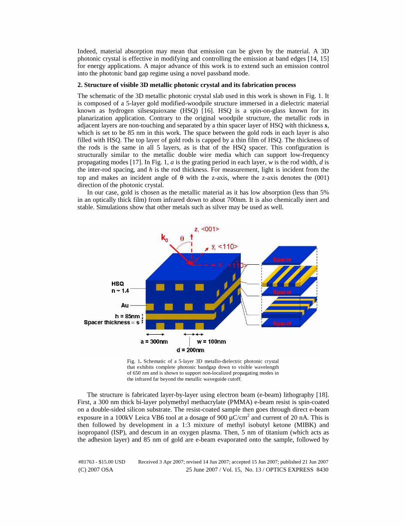
The schematic of the 3D metallic photonic crystal slab used in this work is shown in Fig. 1. It is composed of a 5-layer gold modified-woodpile structure immersed in a dielectric material known as hydrogen silsesquioxane (HSQ) [16]. HSQ is a spin-on-glass known for its planarization application. Contrary to the original woodpile structure, the metallic rods in adjacent layers are non-touching and separated by a thin spacer layer of HSQ with thickness s, which is set to be 85 nm in this work. The space between the gold rods in each layer is also filled with HSQ. The top layer of gold rods is capped by a thin film of HSQ. The thickness of the rods is the same in all 5 layers, as is that of the HSQ spacer. This configuration is structurally similar to the metallic double wire media which can support low-frequency propagating modes [17]. In Fig. 1, a is the grating period in each layer, w is the rod width, d is the inter-rod spacing, and h is the rod thickness. For measurement, light is incident from the top and makes an incident angle of θ with the z-axis, where the z-axis denotes the (001) direction of the photonic crystal.
In our case, gold is chosen as the metallic material as it has low absorption (less than 5% in an optically thick film) from infrared down to about 700nm. It is also chemically inert and stable. Simulations show that other metals such as silver may be used as well.
The structure is fabricated layer-by-layer using electron beam (e-beam) lithography [18]. First, a 300 nm thick bi-layer polymethyl methacrylate (PMMA) e-beam resist is spin-coated on a double-sided silicon substrate. The resist-coated sample then goes through direct e-beam exposure in a 100kV Leica VB6 tool at a dosage of 900 μC/cm2 and current of 20 nA. This is then followed by development in a 1:3 mixture of methyl isobutyl ketone (MIBK) and isopropanol (ISP), and descum in an oxygen plasma. Then, 5 nm of titanium (which acts as the adhesion layer) and 85 nm of gold are e-beam evaporated onto the sample, followed by
Fig. 1. Schematic of a 5-layer 3D metallo-dielectric photonic crystal that exhibits complete photonic bandgap down to visible wavelength of 650 nm and is shown to support non-localized propagating modes in the infrared far beyond the metallic waveguide cutoff.
#81763 - $15.00 USD Received 3 Apr 2007; revised 14 Jun 2007; accepted 15 Jun 2007; published 21 Jun 2007
(C) 2007 OSA 25 June 2007 / Vol. 15, No. 13 / OPTICS EXPRESS 8430
liftoff in methylene chloride. This results in the first layer of gold gratings being patterned onto the substrate. To planarize the structure for the next cycle to stack up another layer, a commercially available (Dow Corning) HSQ dissolved in MIBK is spun on with a thickness of 170nm. SEM and AFM imaging show good step coverage and planarization. The HSQ is then cured at 350 0C for 1 hour on a hotplate at atmospheric pressure. The whole process is repeated for the next layer and the cycle can be carried out to the desired number of layers. Alignment between layers is achieved using gold alignment marks deposited in the same step as the first layer gratings. The total sample area is 5 mm x 5 mm obtained by stitching 324 write fields, and the individual field size is around 300 x 300 μm.
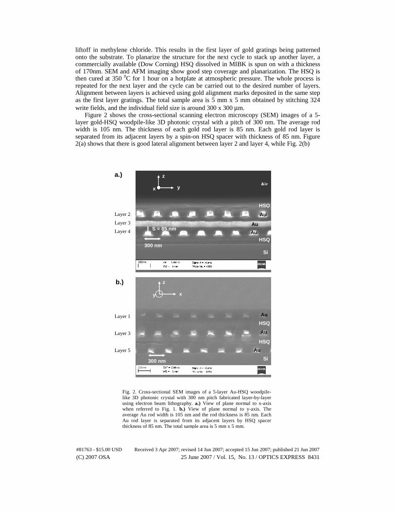
Figure 2 shows the cross-sectional scanning electron microscopy (SEM) images of a 5-layer gold-HSQ woodpile-like 3D photonic crystal with a pitch of 300 nm. The average rod width is 105 nm. The thickness of each gold rod layer is 85 nm. Each gold rod layer is separated from its adjacent layers by a spin-on HSQ spacer with thickness of 85 nm. Figure 2(a) shows that there is good lateral alignment between layer 2 and layer 4, while Fig. 2(b)
Fig. 2. Cross-sectional SEM images of a 5-layer Au-HSQ woodpile-like 3D photonic crystal with 300 nm pitch fabricated layer-by-layer using electron beam lithography. a.) View of plane normal to x-axis when referred to Fig. 1. b.) View of plane normal to y-axis. The average Au rod width is 105 nm and the rod thickness is 85 nm. Each Au rod layer is separated from its adjacent layers by HSQ spacer thickness of 85 nm. The total sample area is 5 mm x 5 mm.
300 nm Si
HSQ
HSQ
Au
Au
Au
Air
S = 85 nm
300 nm
y x
z
x
z
y
Layer 2
Layer 3
Layer 4
Layer 1
Layer 3
Layer 5
b.)
Si
HSQ Au
Au
Au
HSQ
a.)
b.)
#81763 - $15.00 USD Received 3 Apr 2007; revised 14 Jun 2007; accepted 15 Jun 2007; published 21 Jun 2007
(C) 2007 OSA 25 June 2007 / Vol. 15, No. 13 / OPTICS EXPRESS 8431
shows that layer 3 and layer 5 are well aligned with each other. Layer 1 is misaligned with layers 3 and 5 possibly due to the cumulative field-stitching error in the multi-field electron-beam writing over large area. The refractive index of HSQ is measured to be 1.4 by an interference method and shows little variation for wavelength above 700 nm.
3. Fourier transform infrared spectroscopy measurements
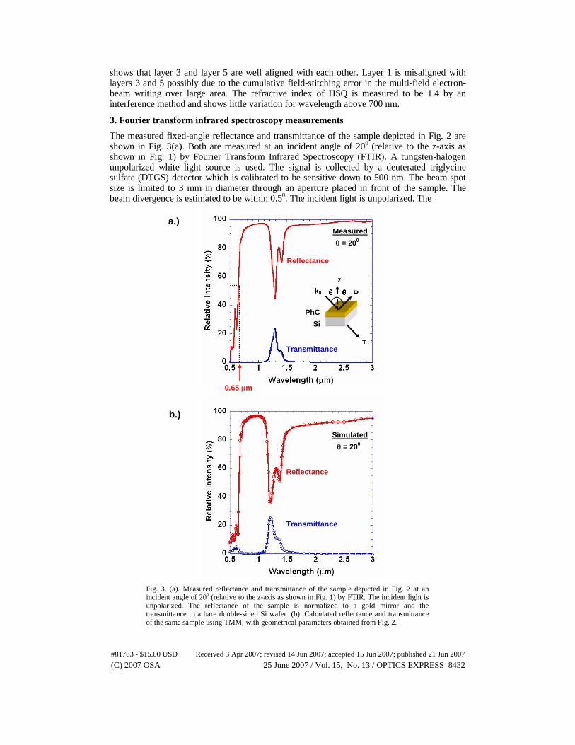
The measured fixed-angle reflectance and transmittance of the sample depicted in Fig. 2 are shown in Fig. 3(a). Both are measured at an incident angle of 200 (relative to the z-axis as shown in Fig. 1) by Fourier Transform Infrared Spectroscopy (FTIR). A tungsten-halogen unpolarized white light source is used. The signal is collected by a deuterated triglycine sulfate (DTGS) detector which is calibrated to be sensitive down to 500 nm. The beam spot size is limited to 3 mm in diameter through an aperture placed in front of the sample. The beam divergence is estimated to be within 0.50. The incident light is unpolarized. The
Reflectance
Transmittance
Measured
θ = 200
0.65 μm
Reflectance
Transmittance
Simulated
θ = 200
a.)
b.)
z
θ k0
PhC
Si
R
T
θ
Fig. 3. (a). Measured reflectance and transmittance of the sample depicted in Fig. 2 at an incident angle of 200 (relative to the z-axis as shown in Fig. 1) by FTIR. The incident light is unpolarized. The reflectance of the sample is normalized to a gold mirror and the transmittance to a bare double-sided Si wafer. (b). Calculated reflectance and transmittance of the same sample using TMM, with geometrical parameters obtained from Fig. 2.
#81763 - $15.00 USD Received 3 Apr 2007; revised 14 Jun 2007; accepted 15 Jun 2007; published 21 Jun 2007
(C) 2007 OSA 25 June 2007 / Vol. 15, No. 13 / OPTICS EXPRESS 8432

reflectance of the sample is normalized to a gold mirror and the transmittance to a bare double-sided silicon wafer.
The data shows a photonic bandgap extending into the visible wavelength range with a band-edge at around 650 nm where it reaches 50% reflectance. In the infrared, the photonic bandgap has very high reflectance as is characteristic of metallic crystals and extends to beyond 3 μm. It is important to note that in the visible region the structure gives rise to photonic bandgap effect as opposed to having just the same characteristics of a uniform gold film of the same total thickness. This is evident at the bottom of the band-edge at 500 nm, where the reflectance drops to less than 10% of a uniform gold film. It is known that enhancement of absorption as well as appearance of transmission window can occur at the band-edge of a 3D metallic photonic crystal [5]. This can be exploited for visible applications through, for example, incorporation of active light emitting materials within the photonic crystal.
The data also shows a narrow transmission band well within the high-reflectance region with peak transmittance of 25% at a wavelength of λ1,exp = 1.3 μm and a secondary peak of just below 10% at λ2,exp = 1.4 μm. There is a corresponding “double-dip” in the reflectance that matches the positions of the transmittance peaks. Note that the slit opening d (see Fig. 1) between individual gold lines in each layer is only d = 200 nm, and that (nHSQ · d) / λ1,exp = 0.215 while the perfect-conducting metallic waveguide cutoff condition is (nHSQ · d) / λcutoff = 0.5. The observed passband modes are thus located far beyond the metallic waveguide cutoff of the structure.
Shown in Fig. 3(b) are the calculated reflectance and transmittance of the same sample using Transfer Matrix Method (TMM) [19], with geometrical parameters measured from Fig. 2 and realistic metallic dielectric constants taking into account the frequency-dependent complex permittivity of gold [20] were used. The calculated band-edge position matches the measured data well. Two reflectance dips appear at λ1,cal = 1.2 μm and λ2,cal = 1.35 μm in the calculation. The calculated position, magnitude and shape of the reflectance dips and transmittance peak agree well with the measurement, adding further evidence to the existence of the propagating modes.
To investigate the effect of incident angle on the optical characteristics of the 3D metallic structure, variable-angle FTIR spectroscopy is performed in reflectance mode. Figure 4 shows the measured tilt-angle reflectance of the sample depicted in Fig. 2 at incident angles from 200 to 600 at 100 increments. The data for 200 is re-plotted here from Fig. 3 for completeness. The tilt-angle geometry is as shown in the inset. The data shows a band-edge fixed at visible wavelength of around 650 nm indicating a 3D complete bandgap exists above this wavelength. It also shows consistent high-reflectance extending to beyond 3 μm in the infrared. Within the high-reflectance region, the “double-dip” in reflectance clearly shifts to shorter wavelength (“blue-shifts”) with incident angle and without change in overall spectral shape. The total spectral shift is about 200 nm for the measurement range. The data shows that in striking contrast to defect modes induced by a 3D cavity resulting from point defect, the observed passband mode is angular dependent and does not exhibit a characteristic of a 3D cavity [21].
FTIR-reflectance measurement is also performed using a microscope that focuses normal incident light to a 50 μm by 50 μm spot size to probe the reflectance at 5 random surface spots on the same sample. It is found that the spectral positions as well as the magnitude of the reflectance dip differ by less than 1.7% both across the measured sample points and with the mainbench results. Thus it appears that the observed passband mode exists across the entire sample area, further demonstrating that it does not originate from unintentional point defects (e.g. 3D cavity) or line defects (e.g. waveguide).
#81763 - $15.00 USD Received 3 Apr 2007; revised 14 Jun 2007; accepted 15 Jun 2007; published 21 Jun 2007
(C) 2007 OSA 25 June 2007 / Vol. 15, No. 13 / OPTICS EXPRESS 8433
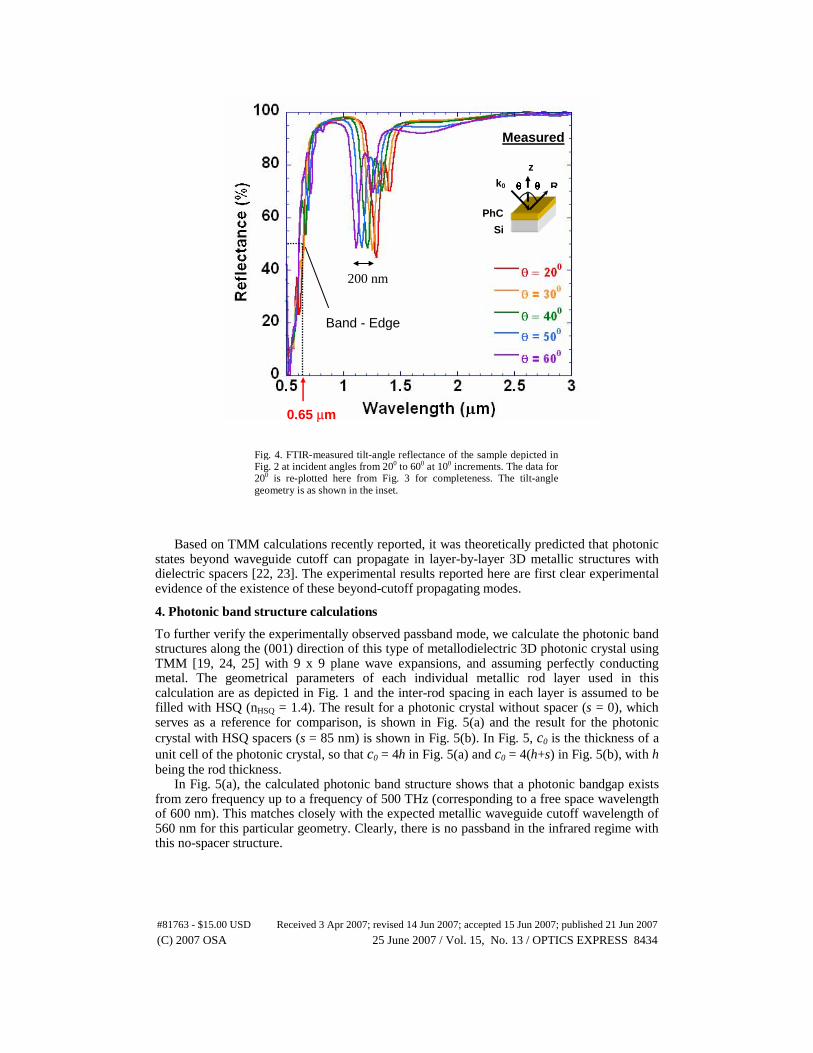
Based on TMM calculations recently reported, it was theoretically predicted that photonic states beyond waveguide cutoff can propagate in layer-by-layer 3D metallic structures with dielectric spacers [22, 23]. The experimental results reported here are first clear experimental evidence of the existence of these beyond-cutoff propagating modes.
4. Photonic band structure calculations
To further verify the experimentally observed passband mode, we calculate the photonic band structures along the (001) direction of this type of metallodielectric 3D photonic crystal using TMM [19, 24, 25] with 9 x 9 plane wave expansions, and assuming perfectly conducting metal. The geometrical parameters of each individual metallic rod layer used in this calculation are as depicted in Fig. 1 and the inter-rod spacing in each layer is assumed to be filled with HSQ (nHSQ = 1.4). The result for a photonic crystal without spacer (s = 0), which serves as a reference for comparison, is shown in Fig. 5(a) and the result for the photonic crystal with HSQ spacers (s = 85 nm) is shown in Fig. 5(b). In Fig. 5, c0 is the thickness of a unit cell of the photonic crystal, so that c0 = 4h in Fig. 5(a) and c0 = 4(h+s) in Fig. 5(b), with h being the rod thickness.
In Fig. 5(a), the calculated photonic band structure shows that a photonic bandgap exists from zero frequency up to a frequency of 500 THz (corresponding to a free space wavelength of 600 nm). This matches closely with the expected metallic waveguide cutoff wavelength of 560 nm for this particular geometry. Clearly, there is no passband in the infrared regime with this no-spacer structure.
200 nm
Measured
Band - Edge
0.65 μm
z
θ k0
PhC
Si
R θ
Fig. 4. FTIR-measured tilt-angle reflectance of the sample depicted in Fig. 2 at incident angles from 200 to 600 at 100 increments. The data for 200 is re-plotted here from Fig. 3 for completeness. The tilt-angle geometry is as shown in the inset.
#81763 - $15.00 USD Received 3 Apr 2007; revised 14 Jun 2007; accepted 15 Jun 2007; published 21 Jun 2007
(C) 2007 OSA 25 June 2007 / Vol. 15, No. 13 / OPTICS EXPRESS 8434
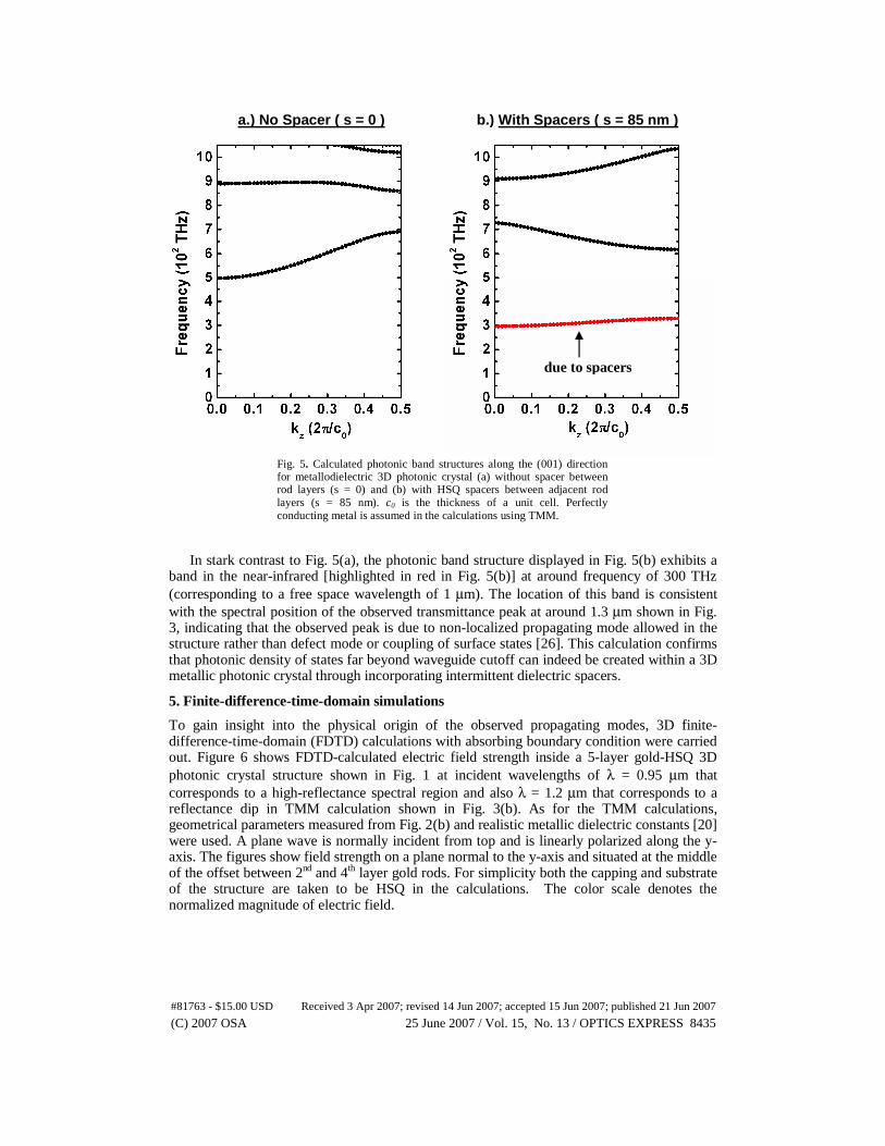
In stark contrast to Fig. 5(a), the photonic band structure displayed in Fig. 5(b) exhibits a band in the near-infrared [highlighted in red in Fig. 5(b)] at around frequency of 300 THz (corresponding to a free space wavelength of 1 μm). The location of this band is consistent with the spectral position of the observed transmittance peak at around 1.3 μm shown in Fig. 3, indicating that the observed peak is due to non-localized propagating mode allowed in the structure rather than defect mode or coupling of surface states [26]. This calculation confirms that photonic density of states far beyond waveguide cutoff can indeed be created within a 3D metallic photonic crystal through incorporating intermittent dielectric spacers.
5. Finite-difference-time-domain simulations
To gain insight into the physical origin of the observed propagating modes, 3D finite-difference-time-domain (FDTD) calculations with absorbing boundary condition were carried out. Figure 6 shows FDTD-calculated electric field strength inside a 5-layer gold-HSQ 3D photonic crystal structure shown in Fig. 1 at incident wavelengths of λ = 0.95 μm that corresponds to a high-reflectance spectral region and also λ = 1.2 μm that corresponds to a reflectance dip in TMM calculation shown in Fig. 3(b). As for the TMM calculations, geometrical parameters measured from Fig. 2(b) and realistic metallic dielectric constants [20] were used. A plane wave is normally incident from top and is linearly polarized along the y-axis. The figures show field strength on a plane normal to the y-axis and situated at the middle of the offset between 2nd and 4th layer gold rods. For simplicity both the capping and substrate of the structure are taken to be HSQ in the calculations. The color scale denotes the normalized magnitude of electric field.
due to spacers
a.) No Spacer ( s = 0 ) b.) With Spacers ( s = 85 nm )
Fig. 5. Calculated photonic band structures along the (001) direction for metallodielectric 3D photonic crystal (a) without spacer between rod layers (s = 0) and (b) with HSQ spacers between adjacent rod layers (s = 85 nm). c0 is the thickness of a unit cell. Perfectly conducting metal is assumed in the calculations using TMM.
#81763 - $15.00 USD Received 3 Apr 2007; revised 14 Jun 2007; accepted 15 Jun 2007; published 21 Jun 2007
(C) 2007 OSA 25 June 2007 / Vol. 15, No. 13 / OPTICS EXPRESS 8435
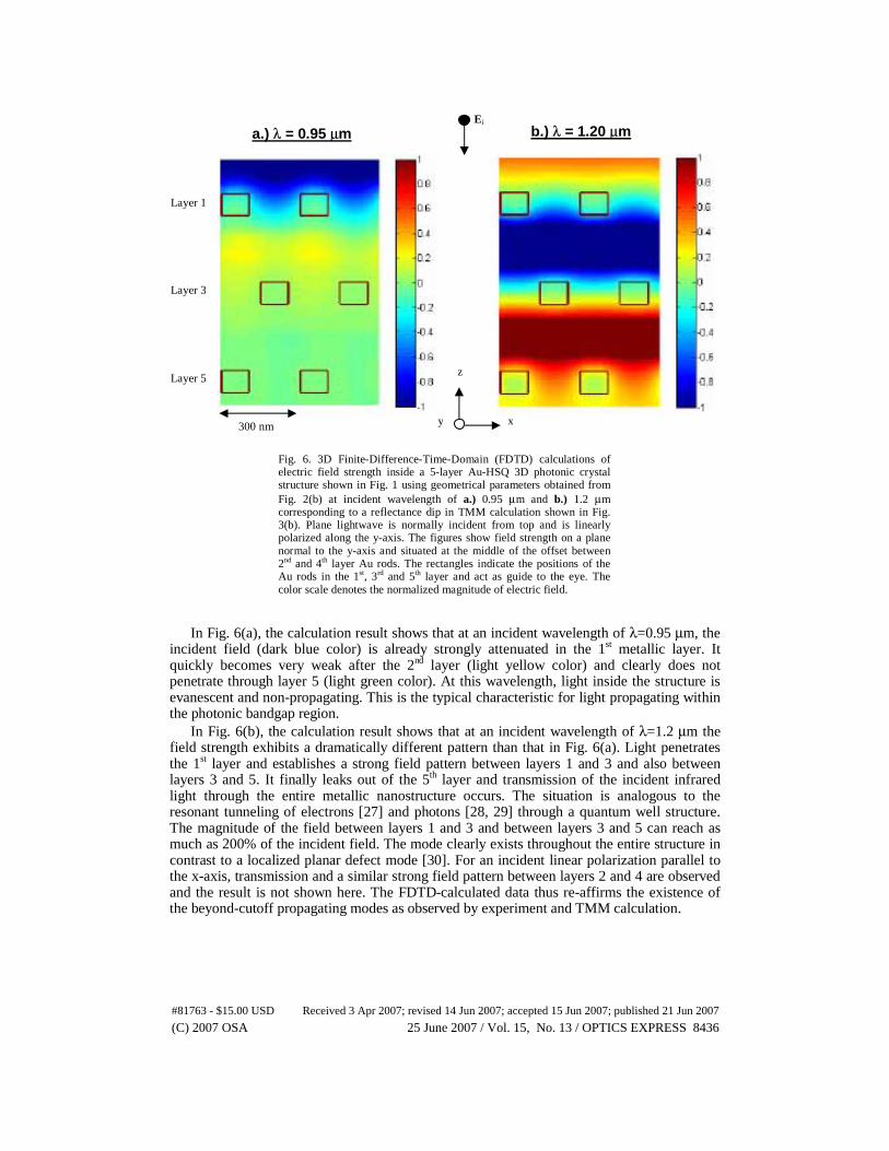
In Fig. 6(a), the calculation result shows that at an incident wavelength of λ=0.95 μm, the incident field (dark blue color) is already strongly attenuated in the 1st metallic layer. It quickly becomes very weak after the 2nd layer (light yellow color) and clearly does not penetrate through layer 5 (light green color). At this wavelength, light inside the structure is evanescent and non-propagating. This is the typical characteristic for light propagating within the photonic bandgap region.
In Fig. 6(b), the calculation result shows that at an incident wavelength of λ=1.2 μm the field strength exhibits a dramatically different pattern than that in Fig. 6(a). Light penetrates the 1st layer and establishes a strong field pattern between layers 1 and 3 and also between layers 3 and 5. It finally leaks out of the 5th layer and transmission of the incident infrared light through the entire metallic nanostructure occurs. The situation is analogous to the resonant tunneling of electrons [27] and photons [28, 29] through a quantum well structure. The magnitude of the field between layers 1 and 3 and between layers 3 and 5 can reach as much as 200% of the incident field. The mode clearly exists throughout the entire structure in contrast to a localized planar defect mode [30]. For an incident linear polarization parallel to the x-axis, transmission and a similar strong field pattern between layers 2 and 4 are observed and the result is not shown here. The FDTD-calculated data thus re-affirms the existence of the beyond-cutoff propagating modes as observed by experiment and TMM calculation.
x
z
y
Layer 1
Layer 3
300 nm
Layer 5
a.) λ = 0.95 μm b.) λ = 1.20 μm Ei
Fig. 6. 3D Finite-Difference-Time-Domain (FDTD) calculations of electric field strength inside a 5-layer Au-HSQ 3D photonic crystal structure shown in Fig. 1 using geometrical parameters obtained from Fig. 2(b) at incident wavelength of a.) 0.95 μm and b.) 1.2 μm corresponding to a reflectance dip in TMM calculation shown in Fig. 3(b). Plane lightwave is normally incident from top and is linearly polarized along the y-axis. The figures show field strength on a plane normal to the y-axis and situated at the middle of the offset between 2nd and 4th layer Au rods. The rectangles indicate the positions of the Au rods in the 1st, 3rd and 5th layer and act as guide to the eye. The color scale denotes the normalized magnitude of electric field.
#81763 - $15.00 USD Received 3 Apr 2007; revised 14 Jun 2007; accepted 15 Jun 2007; published 21 Jun 2007
(C) 2007 OSA 25 June 2007 / Vol. 15, No. 13 / OPTICS EXPRESS 8436

6. Discussion
It is well-known that a single layer of metallic gratings can act as a reflector for incident polarization parallel to its lines. The calculation result shown in Fig. 6(b) seems to suggest that with each layer of metallic lines acting as reflector, a cavity is formed between layers 1 and 3, and another cavity is formed between layers 3 and 5. These cavities may have played a role in the physical origin of the observed propagating modes.
This phenomenon may have interesting applications as it opens up the possibilities of new ways of controlling light through introduction of propagating modes and filtering function into a photonic bandgap material without the need for the often difficult writing and aligning of individual defects into 3D structures, or precise alignment of the incident light beam to these defects, thereby greatly reducing the cost and complexity in the fabrication and implementation of structures and devices. In effect, the spacers can serve as an extra design parameter in tailoring the photonic bandgap of this type of metallic photonic crystal. As the appearance of these passband modes does not rely on highly localized defects, it is possible to have large mode volume extending in two dimensions across the entire sample area for emission applications if a layer of active light-emitting material is incorporated as a spacer layer in the structure.
7. Conclusion
In summary, an omnidirectional photonic bandgap down to the visible regime at wavelength of λ = 650 nm has been demonstrated using a metallic woodpile-like structure with shortest pitch (300 nm) to date, which may extend the exploration of applications of full photonic bandgap into the visible. It is also shown experimentally for the first time that if dielectric spacer layers are incorporated into metallic photonic crystal, it is possible to generate non-localized passband modes far beyond the waveguide cutoff of the structure. This result has great potential to facilitate new ways to tailor and engineer photonic bandgaps, and possibly opens up new exciting prospects for 3D photonic crystals in many applications such as light-emitting devices.
Acknowledgments
The authors thank Prof. H.C. Chang of National Taiwan University for the use of 3D FDTD code. Fabrication of sample was done at the Cornell NanoScale Science and Technology Facility (CNF). Dr. Shawn-Yu Lin would like to acknowledge the financial support of DOE-BES under grant number DE-FG02-06ER46347 and AFOSR under grant number FA95500610431.
#81763 - $15.00 USD Received 3 Apr 2007; revised 14 Jun 2007; accepted 15 Jun 2007; published 21 Jun 2007
(C) 2007 OSA 25 June 2007 / Vol. 15, No. 13 / OPTICS EXPRESS 8437