Embed Size (px)
Citation preview

®
April 2002 1/16
AN1546- APPLICATION NOTE
VIPower: SELF–OSCILLATING CONVERTER USINGVK05CFL FOR COMPACT FLUORESCENT LAMPS
N. Aiello - S. Messina
ABSTRACTThis application note introduces a new self–oscillating converter based on VK05CFL device to drive“SE”, “DE”, and “TE” fluorescent tubes. The design is intended for 5 to 23W fluorescent lamps and 110V,230V ± 20% main voltage.
1. INTRODUCTIONCompact fluorescent lamps are the most popular in the consumer market because compared to thetraditional incandescent lamps they offer the following advantages:- Low power consumption (about 80% lower);- Very high brightness (five times higher);- Very long life (from five to ten times higher).The proposed converter is based on the new VK05CFL VIPower device in half bridge configuration andoffers the following economical benefits:- Monolithic solution with Power and control part on the same chip;- No saturable coil transformer is required;- Reduced number of component with consequent PCB miniaturization;- Single device for all CFL power range, 5W ÷ 23W.
2. THE BALLAST CONCEPTWhen a fluorescent lamp is turned on, the main voltage is not sufficient to cause the initial ionization. Anelement is needed to provide high voltage across the tube to start the process.Figure 1 schematically shows the relationship between the voltage and the current of the arc dischargein a fluorescent lamp.
Figure 1: Static volt-ampere characteristic of a gas discharge
2/16
AN1546 - APPLICATION NOTE
There is a region where the arc discharge characteristic has a negative slope: in this region most of thedischarge lamps operate. To prevent current runaway and ensure stable operation from a constantvoltage power supply the negative characteristic must be counterbalanced by a circuit element orcomponent having positive characteristic. This element is called ballast.
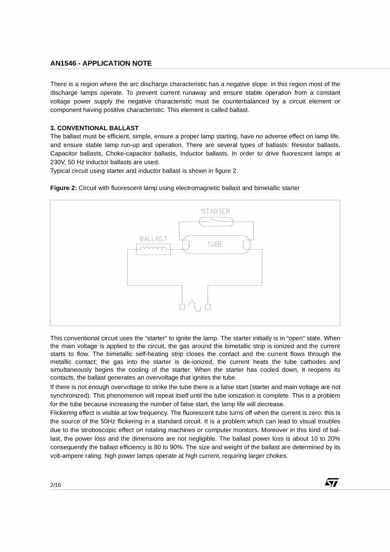
3. CONVENTIONAL BALLASTThe ballast must be efficient, simple, ensure a proper lamp starting, have no adverse effect on lamp life,and ensure stable lamp run-up and operation. There are several types of ballasts: Resistor ballasts,Capacitor ballasts, Choke-capacitor ballasts, Inductor ballasts. In order to drive fluorescent lamps at230V, 50 Hz inductor ballasts are used.Typical circuit using starter and inductor ballast is shown in figure 2.
Figure 2: Circuit with fluorescent lamp using electromagnetic ballast and bimetallic starter
This conventional circuit uses the “starter” to ignite the lamp. The starter initially is in “open” state. Whenthe main voltage is applied to the circuit, the gas around the bimetallic strip is ionized and the currentstarts to flow. The bimetallic self-heating strip closes the contact and the current flows through themetallic contact; the gas into the starter is de-ionized, the current heats the tube cathodes andsimultaneously begins the cooling of the starter. When the starter has cooled down, it reopens itscontacts, the ballast generates an overvoltage that ignites the tube.
If there is not enough overvoltage to strike the tube there is a false start (starter and main voltage are notsynchronized). This phenomenon will repeat itself until the tube ionization is complete. This is a problemfor the tube because increasing the number of false start, the lamp life will decrease.Flickering effect is visible at low frequency. The fluorescent tube turns off when the current is zero: this isthe source of the 50Hz flickering in a standard circuit. It is a problem which can lead to visual troublesdue to the stroboscopic effect on rotating machines or computer monitors. Moreover in this kind of bal-last, the power loss and the dimensions are not negligible. The ballast power loss is about 10 to 20%consequently the ballast efficiency is 80 to 90%. The size and weight of the ballast are determined by itsvolt-ampere rating: high power lamps operate at high current, requiring larger chokes.
3/16
AN1546 - APPLICATION NOTE
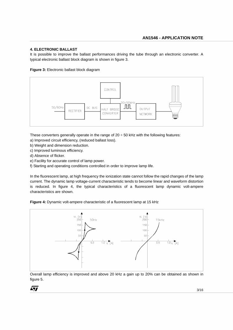
4. ELECTRONIC BALLASTIt is possible to improve the ballast performances driving the tube through an electronic converter. Atypical electronic ballast block diagram is shown in figure 3.
Figure 3: Electronic ballast block diagram
These converters generally operate in the range of 20 ÷ 50 kHz with the following features:a) Improved circuit efficiency, (reduced ballast loss).b) Weight and dimension reduction.c) Improved luminous efficiency.d) Absence of flicker.e) Facility for accurate control of lamp power.f) Starting and operating conditions controlled in order to improve lamp life.
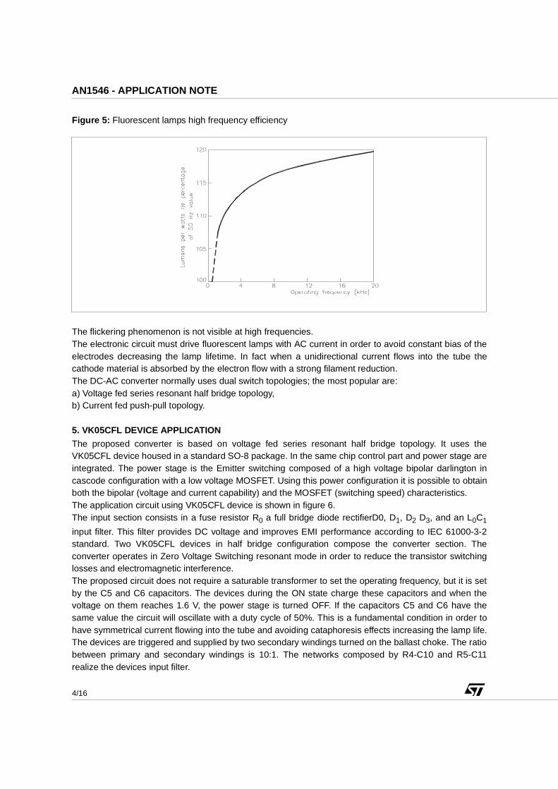
In the fluorescent lamp, at high frequency the ionization state cannot follow the rapid changes of the lampcurrent. The dynamic lamp voltage-current characteristic tends to become linear and waveform distortionis reduced. In figure 4, the typical characteristics of a fluorescent lamp dynamic volt-amperecharacteristics are shown.
Figure 4: Dynamic volt-ampere characteristic of a fluorescent lamp at 15 kHz
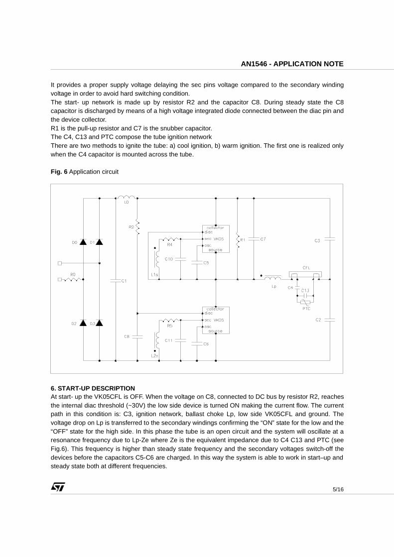
Overall lamp efficiency is improved and above 20 kHz a gain up to 20% can be obtained as shown infigure 5.
4/16
AN1546 - APPLICATION NOTE
Figure 5: Fluorescent lamps high frequency efficiency
The flickering phenomenon is not visible at high frequencies.The electronic circuit must drive fluorescent lamps with AC current in order to avoid constant bias of theelectrodes decreasing the lamp lifetime. In fact when a unidirectional current flows into the tube thecathode material is absorbed by the electron flow with a strong filament reduction.The DC-AC converter normally uses dual switch topologies; the most popular are:a) Voltage fed series resonant half bridge topology,b) Current fed push-pull topology.
5. VK05CFL DEVICE APPLICATION
The proposed converter is based on voltage fed series resonant half bridge topology. It uses theVK05CFL device housed in a standard SO-8 package. In the same chip control part and power stage areintegrated. The power stage is the Emitter switching composed of a high voltage bipolar darlington incascode configuration with a low voltage MOSFET. Using this power configuration it is possible to obtainboth the bipolar (voltage and current capability) and the MOSFET (switching speed) characteristics.The application circuit using VK05CFL device is shown in figure 6.The input section consists in a fuse resistor R0 a full bridge diode rectifierD0, D1, D2 D3, and an L0C1
input filter. This filter provides DC voltage and improves EMI performance according to IEC 61000-3-2standard. Two VK05CFL devices in half bridge configuration compose the converter section. Theconverter operates in Zero Voltage Switching resonant mode in order to reduce the transistor switchinglosses and electromagnetic interference.The proposed circuit does not require a saturable transformer to set the operating frequency, but it is setby the C5 and C6 capacitors. The devices during the ON state charge these capacitors and when thevoltage on them reaches 1.6 V, the power stage is turned OFF. If the capacitors C5 and C6 have thesame value the circuit will oscillate with a duty cycle of 50%. This is a fundamental condition in order tohave symmetrical current flowing into the tube and avoiding cataphoresis effects increasing the lamp life.The devices are triggered and supplied by two secondary windings turned on the ballast choke. The ratiobetween primary and secondary windings is 10:1. The networks composed by R4-C10 and R5-C11realize the devices input filter.
5/16
AN1546 - APPLICATION NOTE
It provides a proper supply voltage delaying the sec pins voltage compared to the secondary windingvoltage in order to avoid hard switching condition.The start- up network is made up by resistor R2 and the capacitor C8. During steady state the C8capacitor is discharged by means of a high voltage integrated diode connected between the diac pin andthe device collector.R1 is the pull-up resistor and C7 is the snubber capacitor.The C4, C13 and PTC compose the tube ignition networkThere are two methods to ignite the tube: a) cool ignition, b) warm ignition. The first one is realized onlywhen the C4 capacitor is mounted across the tube.
Fig. 6 Application circuit
6. START-UP DESCRIPTIONAt start- up the VK05CFL is OFF. When the voltage on C8, connected to DC bus by resistor R2, reachesthe internal diac threshold (~30V) the low side device is turned ON making the current flow. The currentpath in this condition is: C3, ignition network, ballast choke Lp, low side VK05CFL and ground. Thevoltage drop on Lp is transferred to the secondary windings confirming the “ON” state for the low and the“OFF” state for the high side. In this phase the tube is an open circuit and the system will oscillate at aresonance frequency due to Lp-Ze where Ze is the equivalent impedance due to C4 C13 and PTC (seeFig.6). This frequency is higher than steady state frequency and the secondary voltages switch-off thedevices before the capacitors C5-C6 are charged. In this way the system is able to work in start–up andsteady state both at different frequencies.

6/16
AN1546 - APPLICATION NOTE
Since Ce>>C4
is possible neglect its contribution in the resonance formulae obtaining (cool ignition):
Where: fr = Start-up resonance frequency.
Lp = Ballast choke.
C4 = Tube ignition capacitor.
If warm ignition is applied the fr will be related to the PTC resistance variation.
7. STEADY STATE DESCRIPTIONWhen the tube is ignited the resonance frequency becomes:
Where: f’r = Steady state resonance frequency.
While the steady state frequency is set by two capacitors C5 and C6 connected to osc pin. It is possibleto calculate the steady state frequency with the following relationship:
Where:
Where:
R = Internal resistance = 12 kΩ.C = C4 or C5.tstorage is the power storage time. It is a function of collector peak current and temperature (see datasheet
VK05CFL “ELECTRONIC DRIVER FOR CFL APPLICATION”).tdv/dt is a function of collector peak current snubber capacitor value, and collector voltage
For example if we consider
C5=C6=1.2nF; ton=12 x 103 x 1.2 x 10-9 x 0.91 = 13µs.
tstorage = 0.4ms, and C7 = 680nF, tdv/dt ≈ 0.8µs.
T = 2 x (13+0.4+0.8) = 2 x(14.2) = 28.4µs, ⇒ f = 35 kHz.
32 CCCe += (1)
42
1
CLf
p
r ⋅⋅=
π (2)
r
ep
rf
CLf <<
⋅⋅=
π2
1’
(3)
Tf
1= (4)
dtdvstorageONttt
T/2
++= (5)
2
5nON
lCRt ⋅⋅= (6)
7/16
AN1546 - APPLICATION NOTE
8. SECONDARY FILTER DESIGNAccording to schematic shown in Fig. 6 the R4-C10 R5-C11 filters design must perform with the following
consideration:1) The sec filtered voltage must achieve the device ON at the end of the negative dV/dt and before the
end of the freewheeling diode conduction in order to avoid hard switching or switching-on delay.2) The filtered voltage must be high enough (greater than 5V at the end of ton in order to guarantee the
right working frequency.This second condition is strongly related to the load (power of the tube) because the drop on the chokeprimary winding decreases increasing the load current (see Fig 16). A good choice is to fix the time
constant (τ = R x C) in the range: 1.5µs ÷ 3.3µs.The resistors R4, and R5 must be designed according to power dissipated on them during pre-heatingphase (worst case: higher voltage on the secondary winding).
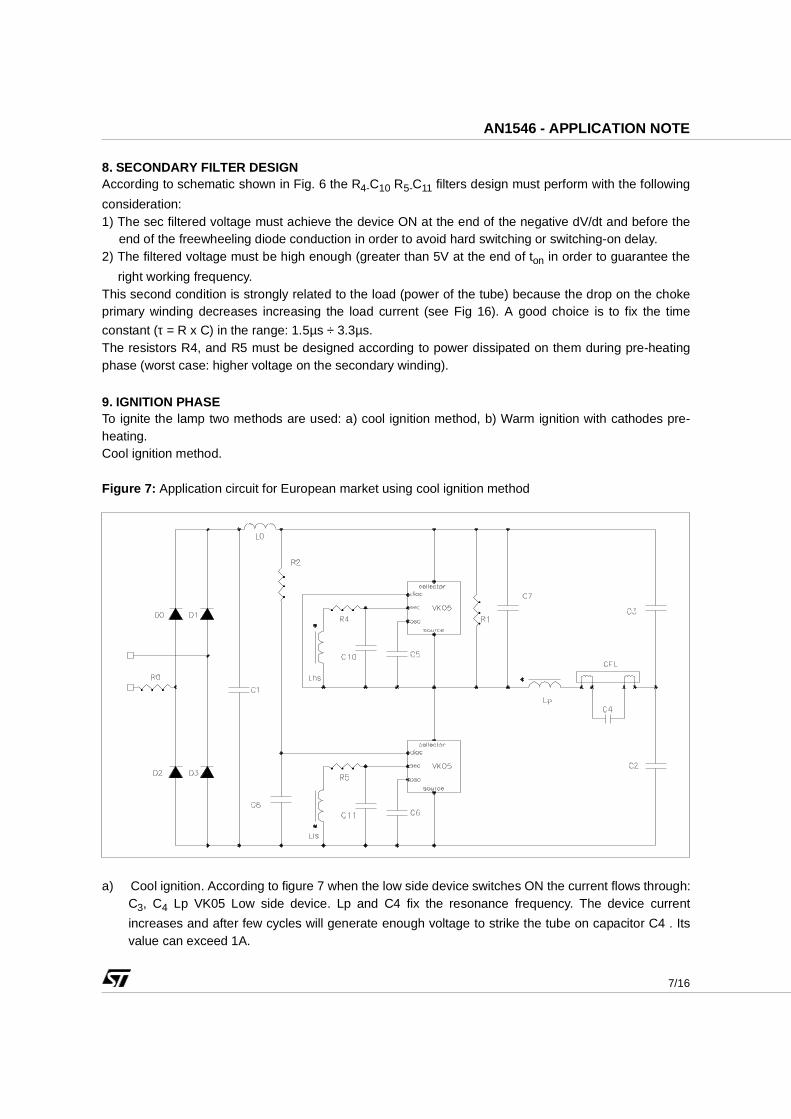
9. IGNITION PHASETo ignite the lamp two methods are used: a) cool ignition method, b) Warm ignition with cathodes pre-heating.Cool ignition method.
Figure 7: Application circuit for European market using cool ignition method
a) Cool ignition. According to figure 7 when the low side device switches ON the current flows through:C3, C4 Lp VK05 Low side device. Lp and C4 fix the resonance frequency. The device current
increases and after few cycles will generate enough voltage to strike the tube on capacitor C4 . Itsvalue can exceed 1A.
8/16
AN1546 - APPLICATION NOTE
b) Warm ignition. In figure 6 a typical application circuit is shown. The warm ignition heats the cathodesin order to increase the electron emission without striking the tube. In this way the followingadvantages are achieved: the tube is ignited with a moderate voltage (lower than cool ignition); thelamp life will increase. In the application board the cathodes pre-heating is obtained using a PTCresistor.
10. VK05CFL APPLICATION BOARD
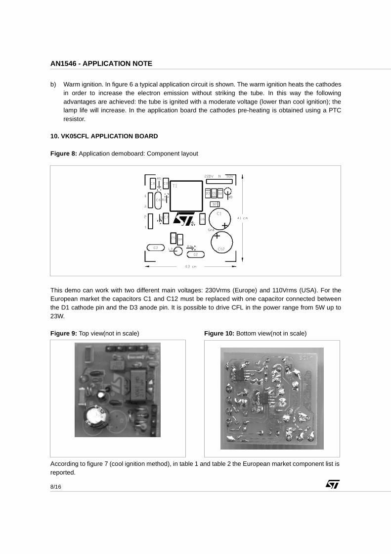
Figure 8: Application demoboard: Component layout
This demo can work with two different main voltages: 230Vrms (Europe) and 110Vrms (USA). For theEuropean market the capacitors C1 and C12 must be replaced with one capacitor connected betweenthe D1 cathode pin and the D3 anode pin. It is possible to drive CFL in the power range from 5W up to23W.
Figure 9: Top view(not in scale) Figure 10: Bottom view(not in scale)
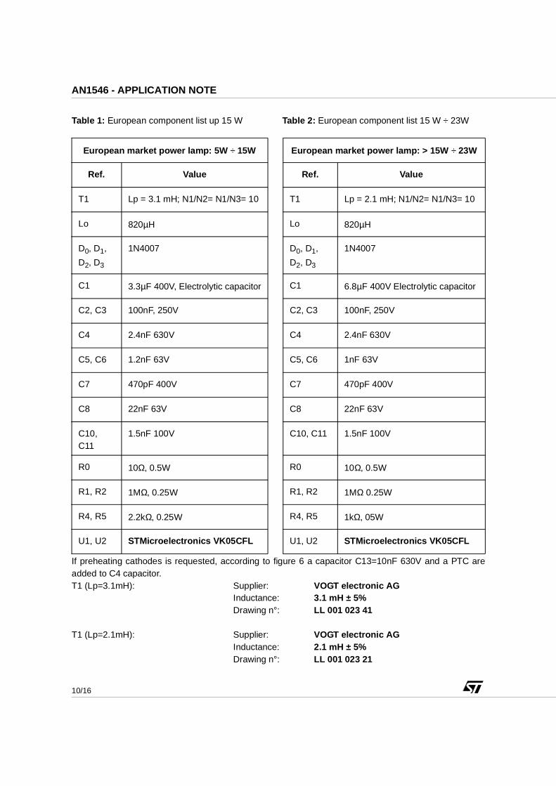
According to figure 7 (cool ignition method), in table 1 and table 2 the European market component list is reported.

9/16
AN1546 - APPLICATION NOTE
For US market the electrical scheme becomes:Figure 11: Application circuit for US market
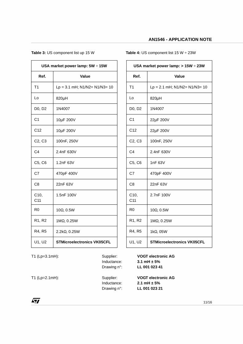
In Table 3 and table 4 the US component list is shown.
10/16
AN1546 - APPLICATION NOTE
Table 1: European component list up 15 W Table 2: European component list 15 W ÷ 23W
If preheating cathodes is requested, according to figure 6 a capacitor C13=10nF 630V and a PTC areadded to C4 capacitor.T1 (Lp=3.1mH): Supplier: VOGT electronic AG
Inductance: 3.1 mH ± 5%Drawing n°: LL 001 023 41
T1 (Lp=2.1mH): Supplier: VOGT electronic AGInductance: 2.1 mH ± 5%Drawing n°: LL 001 023 21
European market power lamp: 5W ÷ 15W European market power lamp: > 15W ÷ 23W
Ref. Value Ref. Value
T1 Lp = 3.1 mH; N1/N2= N1/N3= 10 T1 Lp = 2.1 mH; N1/N2= N1/N3= 10
Lo 820µH Lo 820µH
D0, D1,
D2, D3
1N4007 D0, D1,
D2, D3
1N4007
C1 3.3µF 400V, Electrolytic capacitor C1 6.8µF 400V Electrolytic capacitor
C2, C3 100nF, 250V C2, C3 100nF, 250V
C4 2.4nF 630V C4 2.4nF 630V
C5, C6 1.2nF 63V C5, C6 1nF 63V
C7 470pF 400V C7 470pF 400V
C8 22nF 63V C8 22nF 63V
C10, C11
1.5nF 100V C10, C11 1.5nF 100V
R0 10Ω, 0.5W R0 10Ω, 0.5W
R1, R2 1MΩ, 0.25W R1, R2 1MΩ 0.25W
R4, R5 2.2kΩ, 0.25W R4, R5 1kΩ, 05W
U1, U2 STMicroelectronics VK05CFL U1, U2 STMicroelectronics VK05CFL
11/16
AN1546 - APPLICATION NOTE
Table 3: US component list up 15 W Table 4: US component list 15 W ÷ 23W
T1 (Lp=3.1mH): Supplier: VOGT electronic AGInductance: 3.1 mH ± 5%Drawing n°: LL 001 023 41
T1 (Lp=2.1mH): Supplier: VOGT electronic AGInductance: 2.1 mH ± 5%Drawing n°: LL 001 023 21
USA market power lamp: 5W ÷ 15W USA market power lamp: > 15W ÷ 23W
Ref. Value Ref. Value
T1 Lp = 3.1 mH; N1/N2= N1/N3= 10 T1 Lp = 2.1 mH; N1/N2= N1/N3= 10
Lo 820µH Lo 820µH
D0, D2 1N4007 D0, D2 1N4007
C1 10µF 200V C1 22µF 200V
C12 10µF 200V C12 22µF 200V
C2, C3 100nF, 250V C2, C3 100nF, 250V
C4 2.4nF 630V C4 2.4nF 630V
C5, C6 1.2nF 63V C5, C6 1nF 63V
C7 470pF 400V C7 470pF 400V
C8 22nF 63V C8 22nF 63V
C10, C11
1.5nF 100V C10, C11
2.7nF 100V
R0 10Ω, 0.5W R0 10Ω, 0.5W
R1, R2 1MΩ, 0.25W R1, R2 1MΩ, 0.25W
R4, R5 2.2kΩ, 0.25W R4, R5 1kΩ, 05W
U1, U2 STMicroelectronics VK05CFL U1, U2 STMicroelectronics VK05CFL
12/16
AN1546 - APPLICATION NOTE
11. EXPERIMENTAL RESULTSIn this section the evaluation of the dynamic board is reported. The results have been obtainedconsidering the following conditions:a) Main voltage Vmain = 230Vrms
b) Power lamp Plamp = 23W
c) Ambient temperature Ta = 25°C
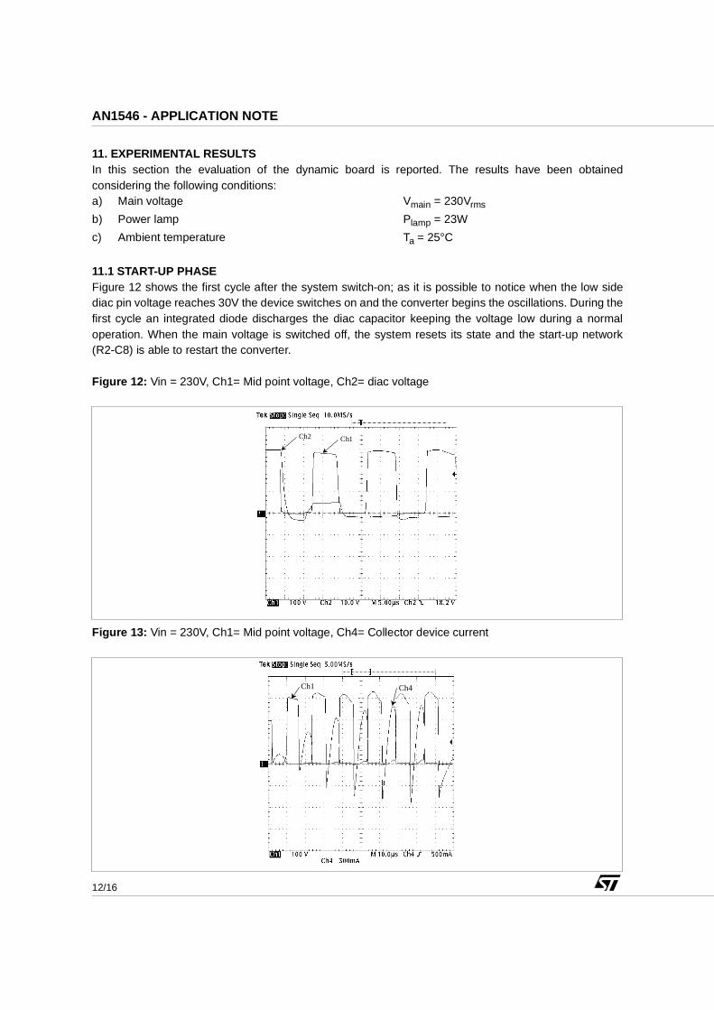
11.1 START-UP PHASEFigure 12 shows the first cycle after the system switch-on; as it is possible to notice when the low sidediac pin voltage reaches 30V the device switches on and the converter begins the oscillations. During thefirst cycle an integrated diode discharges the diac capacitor keeping the voltage low during a normaloperation. When the main voltage is switched off, the system resets its state and the start-up network(R2-C8) is able to restart the converter.
Figure 12: Vin = 230V, Ch1= Mid point voltage, Ch2= diac voltage
Figure 13: Vin = 230V, Ch1= Mid point voltage, Ch4= Collector device current
Ch1 Ch2
Ch1 Ch4

13/16
AN1546 - APPLICATION NOTE
In figure 13 the start up phase with 23W lamp is shown using cool ignition method. The device current(Ch4) rapidly increases; after six cycles its value is able to generate an overvoltage to ignite the tube,using a start-up capacitor.
Figure 14: Vin = 230V,Ch4= Cathodes current during pre-heating phase
In figure 14 the start up phase using 23W lamp with warm ignition method is shown. The ignition time ofthe lamp is lower than 1s.The current lamp with pre-heating circuit is about 3 times lower than the cool ignition, ensuring theheating of the cathodes. Figure 15 shows the cathodes resistance variation in this phase. The hot/coldcathode resistance ratio is about 5.
Figure 15: Vin = 230V Math1 = Cathodes resistance during pre-heating phase
Ch4
Math1
14/16
AN1546 - APPLICATION NOTE
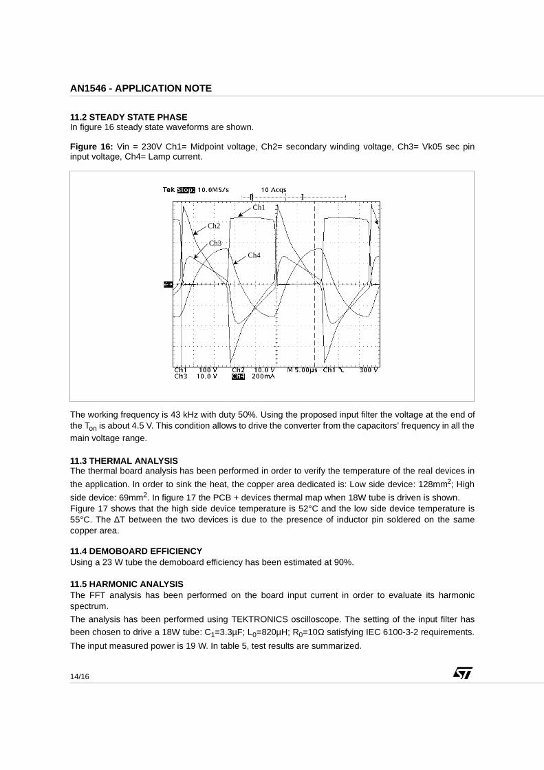
11.2 STEADY STATE PHASEIn figure 16 steady state waveforms are shown.
Figure 16: Vin = 230V Ch1= Midpoint voltage, Ch2= secondary winding voltage, Ch3= Vk05 sec pininput voltage, Ch4= Lamp current.
The working frequency is 43 kHz with duty 50%. Using the proposed input filter the voltage at the end ofthe Ton is about 4.5 V. This condition allows to drive the converter from the capacitors’ frequency in all themain voltage range.
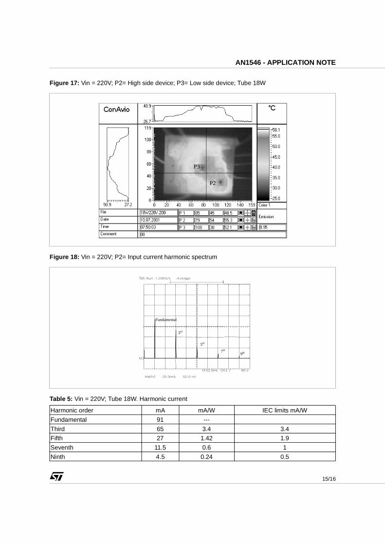
11.3 THERMAL ANALYSISThe thermal board analysis has been performed in order to verify the temperature of the real devices in
the application. In order to sink the heat, the copper area dedicated is: Low side device: 128mm2; High
side device: 69mm2. In figure 17 the PCB + devices thermal map when 18W tube is driven is shown.Figure 17 shows that the high side device temperature is 52°C and the low side device temperature is55°C. The ∆T between the two devices is due to the presence of inductor pin soldered on the samecopper area.
11.4 DEMOBOARD EFFICIENCYUsing a 23 W tube the demoboard efficiency has been estimated at 90%.
11.5 HARMONIC ANALYSISThe FFT analysis has been performed on the board input current in order to evaluate its harmonicspectrum.
The analysis has been performed using TEKTRONICS oscilloscope. The setting of the input filter has
been chosen to drive a 18W tube: C1=3.3µF; L0=820µH; R0=10Ω satisfying IEC 6100-3-2 requirements.
The input measured power is 19 W. In table 5, test results are summarized.
Ch1
Ch3
Ch4
Ch2
15/16
AN1546 - APPLICATION NOTE
Figure 17: Vin = 220V; P2= High side device; P3= Low side device; Tube 18W
Figure 18: Vin = 220V; P2= Input current harmonic spectrum
Table 5: Vin = 220V; Tube 18W. Harmonic current
Harmonic order mA mA/W IEC limits mA/W
Fundamental 91 ---
Third 65 3.4 3.4
Fifth 27 1.42 1.9
Seventh 11.5 0.6 1
Ninth 4.5 0.24 0.5
P2
P3
5th
3rd
7th 9th
Fundamental

16/16
AN1546 - APPLICATION NOTE
Information furnished is believed to be accurate and reliable. However, STMicroelectronics assumes no responsibility for the consequencesof use of such information nor for any infringement of patents or other rights of third parties which may results from its use. No license isgranted by implication or otherwise under any patent or patent rights of STMicroelectronics. Specifications mentioned in this publication aresubject to change without notice. This publication supersedes and replaces all information previously supplied. STMicroelectronics productsare not authorized for use as critical components in life support devices or systems without express written approval of STMicroelectronics.
The ST logo is a trademark of STMicroelectronics
2002 STMicroelectronics - Printed in ITALY- All Rights Reserved.
STMicroelectronics GROUP OF COMPANIESAustralia - Brazil - Canada - China - Finland - France - Germany - Hong Kong - India - Israel - Italy - Japan - Malaysia -
Malta - Morocco - Singapore - Spain - Sweden - Switzerland - United Kingdom - U.S.A.
http://www.st.com