Embed Size (px)
Citation preview
Introduction to Radiation Detectors and Electronics Copyright 1998 by Helmuth SpielerVIII.3. Bipolar Transistors
1
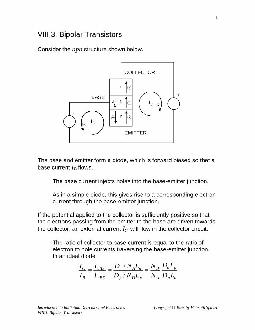
VIII.3. Bipolar Transistors
Consider the npn structure shown below.
The base and emitter form a diode, which is forward biased so that abase current IB flows.
The base current injects holes into the base-emitter junction.
As in a simple diode, this gives rise to a corresponding electron current through the base-emitter junction.
If the potential applied to the collector is sufficiently positive so thatthe electrons passing from the emitter to the base are driven towardsthe collector, an external current IC will flow in the collector circuit.
The ratio of collector to base current is equal to the ratio of electron to hole currents traversing the base-emitter junction.In an ideal diode
n
p
n+
+
IB
IC -
-
+
+ -
-
-
BASE
COLLECTOR
EMITTER
np
pn
A
D
pDp
nAn
pBE
nBE
B
C
LD
LD
N
N
LND
LND
I
I
I
I ===
/
/
Introduction to Radiation Detectors and Electronics Copyright 1998 by Helmuth SpielerVIII.3. Bipolar Transistors
2
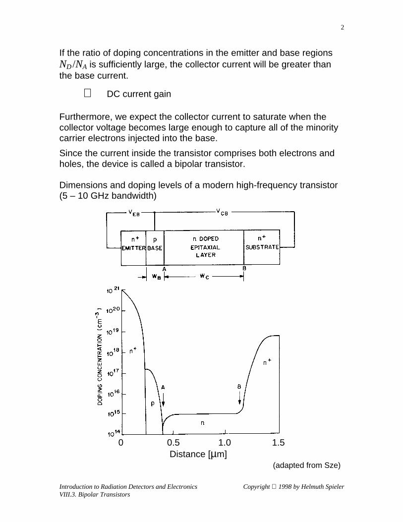
If the ratio of doping concentrations in the emitter and base regionsND /NA is sufficiently large, the collector current will be greater thanthe base current.
⇒ DC current gain
Furthermore, we expect the collector current to saturate when thecollector voltage becomes large enough to capture all of the minoritycarrier electrons injected into the base.
Since the current inside the transistor comprises both electrons andholes, the device is called a bipolar transistor.
Dimensions and doping levels of a modern high-frequency transistor(5 – 10 GHz bandwidth)
0 0.5 1.0 1.5 Distance [µm]
(adapted from Sze)
Introduction to Radiation Detectors and Electronics Copyright 1998 by Helmuth SpielerVIII.3. Bipolar Transistors
3
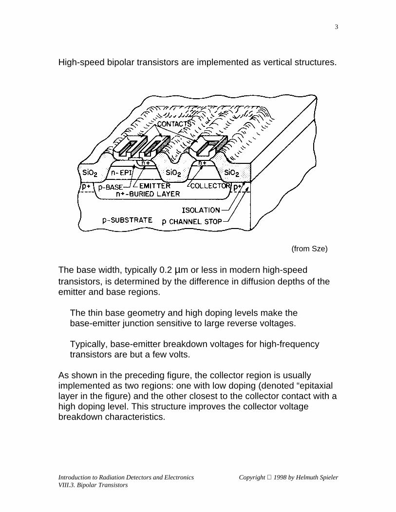
High-speed bipolar transistors are implemented as vertical structures.
(from Sze)
The base width, typically 0.2 µm or less in modern high-speedtransistors, is determined by the difference in diffusion depths of theemitter and base regions.
The thin base geometry and high doping levels make thebase-emitter junction sensitive to large reverse voltages.
Typically, base-emitter breakdown voltages for high-frequencytransistors are but a few volts.
As shown in the preceding figure, the collector region is usuallyimplemented as two regions: one with low doping (denoted “epitaxiallayer in the figure) and the other closest to the collector contact with ahigh doping level. This structure improves the collector voltagebreakdown characteristics.
Introduction to Radiation Detectors and Electronics Copyright 1998 by Helmuth SpielerVIII.3. Bipolar Transistors
4
Quantitative analysis of the bipolar junction transistor (BJT)
1. Holes are injected into the base through the external contact.
The potential distribution drives them towards the emitter.Since they are majority carriers in the base, few will recombine.
Holes entering the base-emitter depletion region will either
a) pass through the depletion region into the emitterb) be lost due to recombination
2. As shown in the discussion of the pn-junction, coupled with thehole current is an electron current originating in the emitter. Thiselectron current will flow towards the collector, driven by the morepositive potential.
These electrons either
a) enter the collector to become the collector currentb) recombine in the base region. The holes required for the
recombination are furnished by the base current.
3. Thus, the base current is the sum of the
a) hole current entering the emitterb) hole losses due to recombination in the base-emitter depletion
regionc) electron losses due to recombination in the base during
transport to the collector
Introduction to Radiation Detectors and Electronics Copyright 1998 by Helmuth SpielerVIII.3. Bipolar Transistors
5
The transport of minority carriers in the base is driven by diffusion, so
At the boundary to the base-emitter depletion region
The equilibrium concentration of electrons in the base is determinedby the base acceptor doping level NAB
At the collector boundary all minority carriers will be immediatelyswept away by the reverse bias field, so that the boundary conditionbecomes
Then the solution of the diffusion equation is
If VBE >> 4kBT/qe the non-equilibrium concentration will dominate
so this simplifies to
002
2
=−
−n
pppn
nn
dx
ndD
τ
TkVqpp
Bbeeenn /0)0( =
0)( =Bp Wn
AB
ip N
nn
2
0 =
n
B
n
B
pp
n
B
npp
L
WL
xW
nn
L
WL
x
nxnsinh
sinh
))0((sinh
sinh
1)( 00
−
−+
−=
0)0( pp nn >>
n
B
n
B
pp
L
WL
xW
nxnsinh
sinh
)0()(
−
=
Introduction to Radiation Detectors and Electronics Copyright 1998 by Helmuth SpielerVIII.3. Bipolar Transistors
6
Since the base width WB in good transistors is much smaller than thediffusion length Ln, the concentration profile can be approximated bya linear distribution.
Now we can evaluate the individual current components.
In this approximation the diffusion current of electrons in the baseregion becomes
where DnB is the diffusion constant of electrons in the base.
Similarly, the diffusion current of holes injected into the emitter, underthe assumption that the emitter depth is much smaller than thediffusion length, is
For the moment, we’ll neglect recombination of holes in the base-emitter depletion region. Under this assumption, the base current is
where AJE is the area of the emitter junction.
−=
Bpp W
xnxn 1)0()(
TkVq
BAB
inBenB
BBEeeWN
nDqJ /
2
=
TkVq
EDE
ipEepE
BBEeeWN
nDqJ /
2
=
JEpEB AJI =
Introduction to Radiation Detectors and Electronics Copyright 1998 by Helmuth SpielerVIII.3. Bipolar Transistors
7
The collector current is primarily the electron current injected into thebase, minus any losses due to recombination during diffusion. Thecollector transport factor
Using the above result this becomes
Recalling that the base width is to be much smaller than the diffusionlength, this expression can be approximated as
The resulting collector current is the diffusion current of electrons inthe base times the transport factor
One of the most interesting parameters of a bipolar transistor is theDC current gain which is the ratio of collector current to base current
n
BT
L
Wcosh
1=α
2
21
1
−≈
n
BT L
Wα
B
CDC I
I=β
TJEnBC AJI α=
0=
===
x
p
Wx
p
T
dx
dn
dx
dn
emitterfrominjectedcurrentelectron
collectorreachingcurrentelectronB
α
Introduction to Radiation Detectors and Electronics Copyright 1998 by Helmuth SpielerVIII.3. Bipolar Transistors
8
Using the above results
Primarily, the DC current gain is determined by the ratio of dopingconcentrations in the emitter and the base.
This simple result reflects the distribution of current in theforward biased diode between electrons and holes.
Transistors with high current gains always have much higher dopinglevels in the emitter than in the base.
BpE
EnB
AB
DEDC
TkVq
EDE
ipEe
TkVq
BAB
inBe
DC
WD
WD
N
N
eWN
nDq
eWN
nDq
BBEe
BBEe
⋅=
=
β
β/
2
/2
Introduction to Radiation Detectors and Electronics Copyright 1998 by Helmuth SpielerVIII.3. Bipolar Transistors
9
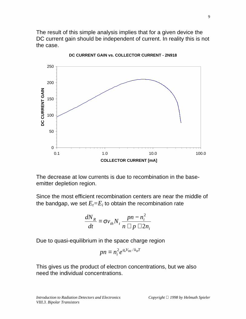
The result of this simple analysis implies that for a given device theDC current gain should be independent of current. In reality this is notthe case.
The decrease at low currents is due to recombination in the base-emitter depletion region.
Since the most efficient recombination centers are near the middle ofthe bandgap, we set Et=Ei to obtain the recombination rate
Due to quasi-equilibrium in the space charge region
This gives us the product of electron concentrations, but we alsoneed the individual concentrations.
i
itth
R
npn
npnNv
dt
dN
2
2
++−= σ
TkVqi
BBEeenpn /2=
DC CURRENT GAIN vs. COLLECTOR CURRENT - 2N918
0
50
100
150
200
250
0.1 1.0 10.0 100.0
COLLECTOR CURRENT [mA]
DC
CU
RR
EN
T G
AIN
Introduction to Radiation Detectors and Electronics Copyright 1998 by Helmuth SpielerVIII.3. Bipolar Transistors
10
For a given forward bias the maximum recombination rate willcoincide with the minimum concentration, i.e.
and since pn= const.
or
at the point of maximum recombination.
Hence, the carrier concentrations are
or
Inserting these concentrations into the expression for therecombination rate yields
This maximum recombination rate will not prevail throughout thedepletion region, but only over a region where the potential changesno more than ~kBT/qe. If we assume that the average field isVBE /WBE, a suitable averaging distance is
Nevertheless, for simplicity assume that recombination is uniformthroughout the depletion region.
0)( =+ npd
dpp
pndndp 2=−=
np =
TkVqi
BBEeenpn 2/==
TkVqi
BBEeenpnpn /222 ===
)1(2
)1(2/
/2
+−= TkVq
i
TkVqi
tthR
BBEe
BBEe
en
enNv
dt
dN σ
BE
BE
e
B
V
W
q
Tkw =
Introduction to Radiation Detectors and Electronics Copyright 1998 by Helmuth SpielerVIII.3. Bipolar Transistors
11
For VBE >> kBT/qe this yields the recombination current to be madeup by holes from the base current
Now the base current becomes
so the DC current gain with recombination is
Because of the factor ½ in the exponent of the recombination term
which can be rewritten in a more informative form as
where β0 is the DC current gain without recombination. Increasing the
concentration of traps Nt decreases the current gain βDC, whereasdecreasing the base width WB reduces the effect of traps. Since asmaller base width translates to increased speed (reduced transittime through the base), fast transistors tend to be less sensitive totrapping.
, )( JERpEB AJJI +=
,
22/
0
2
2
TkVqBE
i
EDE
ipE
BAB
inB
DCBBEeeW
n
WN
nD
WN
nD
−+=
τ
β
TkVqBEitthe
Repr
BBEeeWnNvqdt
dNqJ 2/
2
1 σ≈=
TkVqitthe
TkVq
EDE
ipEe
TkVq
BAB
inBe
DCBBEeBBEe
BBEe
WenNvqeWN
nDq
eWN
nDq
2//2
/2
2
1 σβ
+=
TkVqi
thtB
nB
BEAB
DC BBEeen
vNW
D
WN2/
0
11 σββ
+=
Introduction to Radiation Detectors and Electronics Copyright 1998 by Helmuth SpielerVIII.3. Bipolar Transistors
12
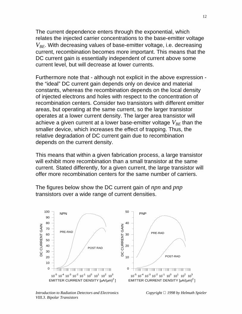
The current dependence enters through the exponential, whichrelates the injected carrier concentrations to the base-emitter voltageVBE. With decreasing values of base-emitter voltage, i.e. decreasingcurrent, recombination becomes more important. This means that theDC current gain is essentially independent of current above somecurrent level, but will decrease at lower currents.
Furthermore note that - although not explicit in the above expression -the “ideal” DC current gain depends only on device and materialconstants, whereas the recombination depends on the local densityof injected electrons and holes with respect to the concentration ofrecombination centers. Consider two transistors with different emitterareas, but operating at the same current, so the larger transistoroperates at a lower current density. The larger area transistor willachieve a given current at a lower base-emitter voltage VBE than thesmaller device, which increases the effect of trapping. Thus, therelative degradation of DC current gain due to recombinationdepends on the current density.
This means that within a given fabrication process, a large transistorwill exhibit more recombination than a small transistor at the samecurrent. Stated differently, for a given current, the large transistor willoffer more recombination centers for the same number of carriers.
The figures below show the DC current gain of npn and pnptransistors over a wide range of current densities.
10-5
10-4
10-3
10-2
10-1
100
101
102
103
EMITTER CURRENT DENSITY [µA/(µm)2 ]
0
10
20
30
40
50
60
70
80
90
100
DC
CU
RR
EN
T G
AIN
PRE-RAD
POST RAD
10-5
10-4
10-3
10-2
10-1
100
101
102
103
EMITTER CURRENT DENSITY [µA/(µm)2 ]
0
10
20
30
40
50
DC
CU
RR
EN
T G
AIN
PRE-RAD
POST-RAD
NPN PNP
Introduction to Radiation Detectors and Electronics Copyright 1998 by Helmuth SpielerVIII.3. Bipolar Transistors
13
As shown in the figures, the DC current gain in modern devices isquite uniform over orders of magnitude of emitter current. Thedecrease in DC current gain at low current densities due to increasedrecombination is apparent. The figures also show the degradation ofcurrent gain after irradiation, here after exposure to the equivalent of1014 minimum ionizing protons/cm2. Radiation damage increases theconcentration of trapping sites Nt proportional to fluence Φ, so theabove equation can be rewritten to express the degradation of currentgain with fluence for a given current density (fixed VBE ).
where the constant K encompasses the device constants andoperating point. In a radiation-damaged transistor the reduction incurrent gain for a given DC current will be less for smaller devicesand faster transistors tend to be less sensitive to radiation damage.
Why does the DC current gain drop off at high currents?
a) with increasing current the high field region shifts towards thecollector, effectively increasing the base width (“Kirk effect”).
b) at high current levels the injected carrier concentration becomescomparable with the bulk doping.
a) reduction in injection efficiencyb) at very high current densities band-gap narrowing
c) voltage drops in base and emitter resistance
d) Auger recombination
Auger effect:
In an atomic transition, instead of photon emission an electronis emitted.
Assume a Kα transition (i.e. from the L to the K shell).
Φ+= KDC 0
11
ββ
Introduction to Radiation Detectors and Electronics Copyright 1998 by Helmuth SpielerVIII.3. Bipolar Transistors
14
If the ionization of an L electron is less than the Kα transitionenergy, instead of a photon an L electron can be emitted withan energy
In semiconductors the Auger effect manifests itself asrecombination of an electron-hole pair with emission of anenergetic majority carrier.
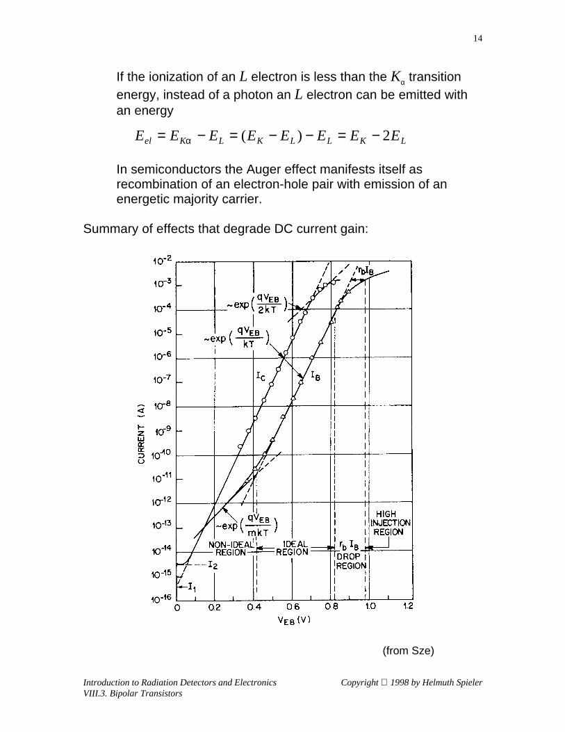
Summary of effects that degrade DC current gain:
(from Sze)
LKLLKLKel EEEEEEEE 2)( −=−−=−= α
Introduction to Radiation Detectors and Electronics Copyright 1998 by Helmuth SpielerVIII.3. Bipolar Transistors
15
Bipolar Transistors in Amplifiers
Although the bipolar transistor is a current driven device, it is oftenconvenient to consider its response to input voltage.
Since the dependence of base current on base-emitter voltage isgiven by the diode equation
The resulting collector current is
The transconductance, i.e. the change in collector current vs. base-emitter voltage
The transconductance depends only on collector current, so for anybipolar transistor – regardless of its internal design – setting thecollector current determines the transconductance.
Since at room temperature kBT/qe= 26 mV
TkVqR
TkVqRB
BBEeBBEe eIeII // )1( ≈−=
TkVqRDCBDCC
BBEeeIII /ββ ==
CB
eTkVq
B
eRDC
BE
Cm I
Tk
qe
Tk
qI
dV
dIg BBEe ==≡ /β
CC
m II
g 40026.0
≈=
Introduction to Radiation Detectors and Electronics Copyright 1998 by Helmuth SpielerVIII.3. Bipolar Transistors
16
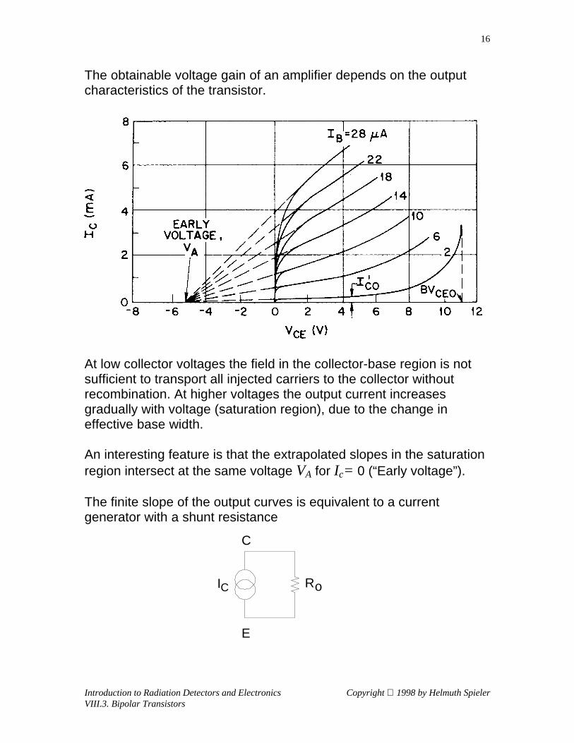
The obtainable voltage gain of an amplifier depends on the outputcharacteristics of the transistor.
At low collector voltages the field in the collector-base region is notsufficient to transport all injected carriers to the collector withoutrecombination. At higher voltages the output current increasesgradually with voltage (saturation region), due to the change ineffective base width.
An interesting feature is that the extrapolated slopes in the saturationregion intersect at the same voltage VA for Ic= 0 (“Early voltage”).
The finite slope of the output curves is equivalent to a currentgenerator with a shunt resistance
IC Ro
C
E
Introduction to Radiation Detectors and Electronics Copyright 1998 by Helmuth SpielerVIII.3. Bipolar Transistors
17
where
K is a device-specific constant of order 1.
The maximum obtainable voltage gain is
which at room temperature is about (40VA K).
Note that to first order the maximum obtainable voltage gain isindependent of current.
Transistors with large Early voltages will allow higher voltage gain.
C
Ao I
VKR =
eB
A
C
A
eB
Como
BE
Cv qTk
VK
I
VK
qTk
IRgR
dV
dIA
/
/max, ====
Introduction to Radiation Detectors and Electronics Copyright 1998 by Helmuth SpielerVIII.3. Bipolar Transistors
18
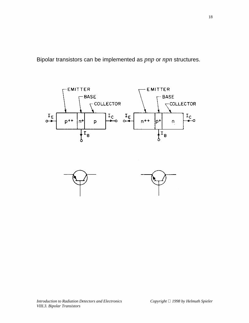
Bipolar transistors can be implemented as pnp or npn structures.
Introduction to Radiation Detectors and Electronics Copyright 1998 by Helmuth SpielerVIII.3. Bipolar Transistors
19
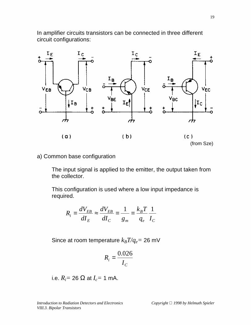
In amplifier circuits transistors can be connected in three differentcircuit configurations:
(from Sze)
a) Common base configuration
The input signal is applied to the emitter, the output taken from the collector.
This configuration is used where a low input impedance is required.
Since at room temperature kBT/qe= 26 mV
i.e. Ri= 26 Ω at Ic= 1 mA.
Ce
B
mC
EB
E
EBi Iq
Tk
gdI
dV
dI
dVR
11 ==≈=
Ci I
R026.0=
Introduction to Radiation Detectors and Electronics Copyright 1998 by Helmuth SpielerVIII.3. Bipolar Transistors
20
b) Common emitter configuration
The input signal is applied to the base, the output taken from the collector.
The input resistance is higher than that of the common base stage.
Since the base current is about βDC times smaller than the emitter current, the input resistance of the common emitter stage is βDC times larger than that of the common base stage.
For βDC = 100 and Ic= 1 mA, Ri= 2600 Ω.
c) Common collector configuration
The signal is applied to the base and the output taken from the emitter (“emitter folower”).
The voltage gain of this configuration cannot exceed 1, but the input resistance can be very high.
Since the load resistance RL introduces local negative feedback, the input resistance depends on the load
The output resistance of the emitter follower is
so at 1 mA collector current Ro= 26 Ω, i.e. although the stage only has unity voltage gain, it does have current gain.
C
DC
e
B
m
DC
C
BEDC
B
BEi Iq
Tk
gdI
dV
dI
dVR
βββ ==≈=
Li RR β≈
mE
BE
E
BEin
out
outo gdI
dV
dI
VVd
dI
dVR
1)( ≈≈−==
Introduction to Radiation Detectors and Electronics Copyright 1998 by Helmuth SpielerVIII.3. Bipolar Transistors
21
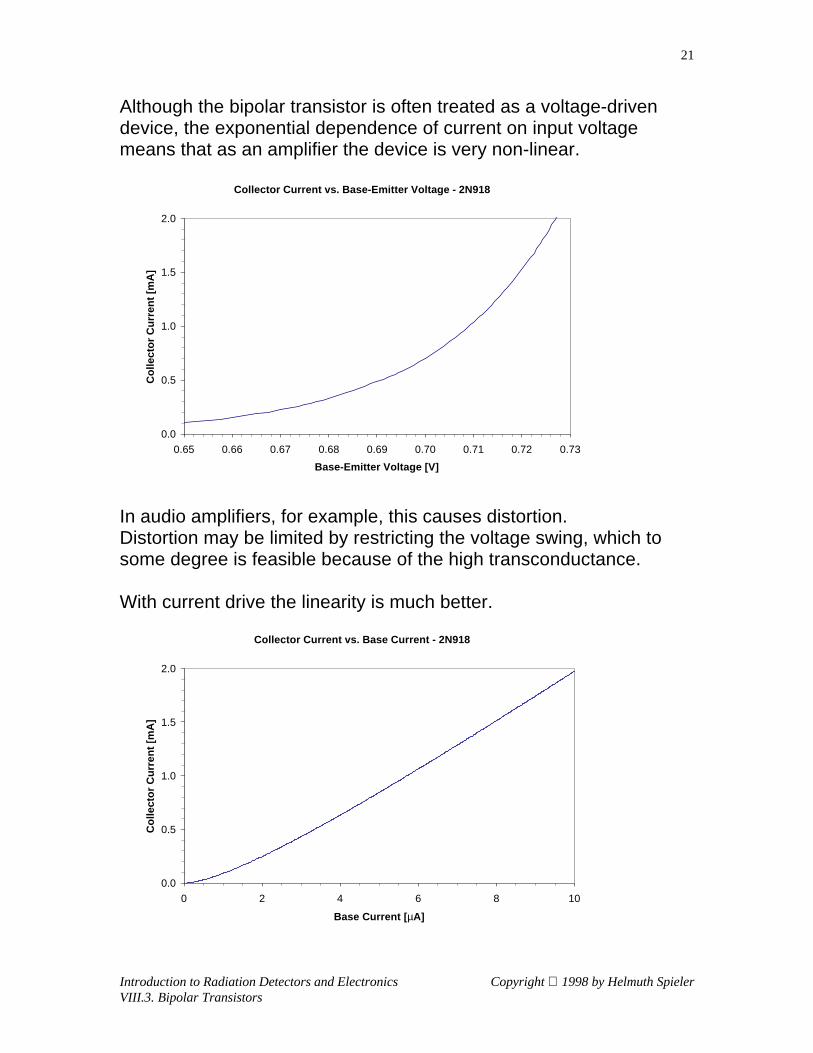
Although the bipolar transistor is often treated as a voltage-drivendevice, the exponential dependence of current on input voltagemeans that as an amplifier the device is very non-linear.
In audio amplifiers, for example, this causes distortion.Distortion may be limited by restricting the voltage swing, which tosome degree is feasible because of the high transconductance.
With current drive the linearity is much better.
Collector Current vs. Base-Emitter Voltage - 2N918
0.0
0.5
1.0
1.5
2.0
0.65 0.66 0.67 0.68 0.69 0.70 0.71 0.72 0.73
Base-Emitter Voltage [V]
Co
llect
or
Cu
rren
t [m
A]
Collector Current vs. Base Current - 2N918
0.0
0.5
1.0
1.5
2.0
0 2 4 6 8 10
Base Current [µA]
Co
llect
or
Cu
rren
t [m
A]