Embed Size (px)
Citation preview
Chapter twoCombinational and Sequential Circuits
2. Combinational and Sequential Circuits2.1. Boolean AlgebraBoolean logic forms the basis for computation in modern binary computer systems. You can represent any algorithm, or any electronic computer circuit, using a system of Boolean equations. After reading this section, you should understand the link among Boolean algebra, truth tables, and Boolean expressions. And later you will link this concept to logic gates and then to the design of common combinational circuits and even to sequential circuits.
Boolean algebra is a deductive mathematical (don’t worry what deductive means now) system closed over the values zero and one. Any binary operator defined over this set of values accepts a pair of Boolean inputs and produces a single Boolean value. For example, the Boolean AND operator accepts two Boolean inputs and produces a single Boolean output (the logical AND of the two inputs).
For any given algebra system, there are some initial assumptions, or postulates, that the system follows. You can deduce additional rules, theorems, and other properties of the system from this basic set of postulates. Boolean algebra systems often employ the following postulates:
Closure. The Boolean system is closed with respect to a binary operator if for every pair of Boolean values, it produces a Boolean result. For example, logical AND is closed in the Boolean system because it accepts only Boolean operands and produces only Boolean results.
Commutatively. A binary operator "%" is said to be commutative if A%B = B%A for all possible Boolean values A and B.
Associatively. A binary operator "%" is said to be associative if (A % B) % C = A % (B % C) for all Boolean values A, B, and C.
Distribution. Two binary operators "%" and "#" are distributive if A % (B # C) = (A % B) # (A % C) for all Boolean values A, B, and C.
Identity. A Boolean value I is said to be the identity element with respect to some binary operator "%" if A % I = A.
Inverse. A Boolean value A is said to be the inverse element of B with respect to some binary operator "%" if (A % B) = (B%A) = I (i.e., B is the opposite value of A in a Boolean system).
For our purposes, we will base Boolean algebra on the following set of operators and values: The two possible values in the Boolean system are zero and one. Often we will call these
values false and true (respectively). The symbol "●" represents the logical AND operation; e.g., A●B is the result of logically
ANDing of the Boolean values A and B. When using single letter variable names, we usually drop the "●" symbol; Therefore, AB also represents the logical AND of the
1
variables A and B (we will also call this the product of A and B). A●B is also represented as AB.
The symbol "+" represents the logical OR operation; e.g., A + B is the result of logically ORing of the Boolean values A and B. (We will also call this the sum of A and B.)
Logical complement, negation, or not, is a unary operator. We will use the (') symbol to denote logical negation. For example, A' denotes the logical NOT of A.
If several different operators appear in a single Boolean expression, the result of the expression depends on the precedence of the operators. We'll use the following precedence (from highest to lowest) for the Boolean operators: parenthesis, logical NOT, logical AND, then logical OR. The logical AND and OR operators are left associative. If two operators with the same precedence are adjacent, you must evaluate them from left to right (i.e., it is called left justified). The logical NOT operation is right associative (or right justified), although it would produce the same result using left or right associatively since it is a unary operator.
2.2. Axioms and Basic Terms of Boolean AlgebraThe followings are set of postulates:
P1: Boolean algebra is closed under the AND, OR, and NOT operations. P2: The identity element with respect to AND is one and OR is zero. There is no identity
element with respect to logical NOT. P3: The AND and OR operators are commutative. P4: AND and OR are distributive with respect to one another. That is, A ● (B + C) = (A
●B) + (A● C) and A + (B● C) = (A + B) ● (A + C). P5: For every value A there exists a value A' such that AA' = 0 and A+A' = 1. This value is
the logical complement (or NOT) of A. P6: AND and OR are both associative. That is, (AB)C = A(BC) and (A+B)+C = A+(B+C). Note
that A●B can also be written as AB for simplicity.You can prove all other theorems in Boolean algebra using these postulates. We will do a formal proof of some of the Theorems; however, it is a good idea to familiarize yourself with some important theorems in Boolean algebra. A sampling includes: Th1: A + A = A Th2: A A = A Th3: A + 0 = A Th4: A 1 = A Th5: A 0 = 0 Th6: A + 1 = 1 Th7: (A + B)' = A' B' Th8: (A B)' = A' + B' Th9: A + AB = A Th10: A (A + B) = A Th11: A + A'B = A+B Th12: A' (A + B') = A'B' Th13: AB + AB' = A Th14: (A'+B') (A' + B) = A'
2
Th15: A + A' = 1 Th16: A A' = 0
Theorems seven and eight above are known as DeMorgan's Theorems after the mathematician who discovered them. DeMorgan’s theorem is a very powerful tool, as can be seen in the next sections.
The theorems above appear in pairs. Each pair (e.g., Th1 & Th2, Th3 & Th4, etc.) form a dual. An important principle in the Boolean algebra system is that of duality. Any valid expression you can create using the postulates and theorems of Boolean algebra remains valid if you interchange the operators and constants appearing in the expression. Specifically, if you exchange the ● and + operators and swap the 0 and 1 values in an expression, you will wind up with an expression that obeys all the rules of Boolean algebra. This does not mean the dual expression computes the same values, it only means that both expressions are legal in the Boolean algebra system. Therefore, this is an easy way to generate a second theorem for any fact you prove in the Boolean algebra system.
We will use these theorems to show that two Boolean equations are identical. This is an important operation when attempting to produce canonical representations (discussed later) of a Boolean expression or when simplifying a Boolean expression.
2.3. Boolean Functions and Truth TablesA Boolean expression is a sequence of zeros, ones, and literals separated by Boolean operators. A literal is a primed (negated) or un primed variable name.‐ For our purposes, all variable names will be a single alphabetic character. A Boolean function is a specific Boolean expression; we will generally give Boolean functions the name "F" with a possible subscript.For example, consider the following Boolean function: F0 = AB+C
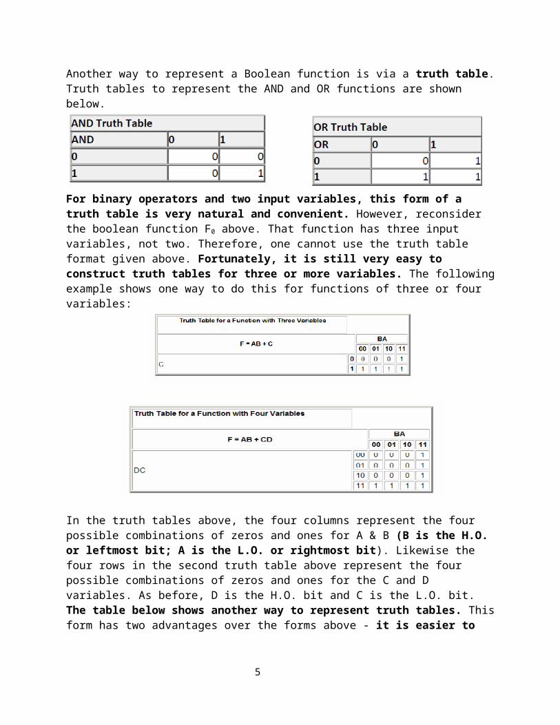
This function computes the logical AND of A and B and then logically ORs this result with C. If A=1, B=0, and C=1, then F0 returns the value one (1●0 + 1 = 1).Another way to represent a Boolean function is via a truth table. Truth tables to represent the AND and OR functions are shown below.
For binary operators and two input variables, this form of a truth table is very natural and convenient. However, reconsider the boolean function F0 above. That function has three input variables, not two. Therefore, one cannot use the truth table format given above. Fortunately, it is still very easy to construct truth tables for three or more variables. The following example shows one way to do this for functions of three or four variables:
3
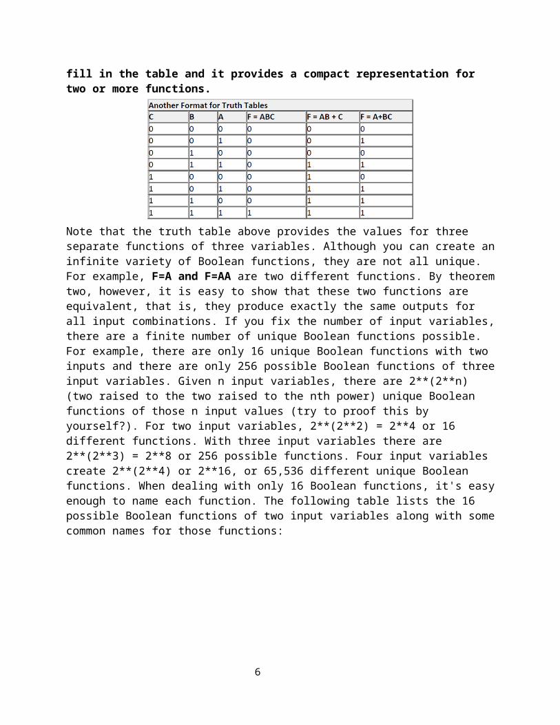
In the truth tables above, the four columns represent the four possible combinations of zeros and ones for A & B (B is the H.O. or leftmost bit; A is the L.O. or rightmost bit). Likewise the four rows in the second truth table above represent the four possible combinations of zeros and ones for the C and D variables. As before, D is the H.O. bit and C is the L.O. bit. The table below shows another way to represent truth tables. This form has two advantages over the forms above ‐ it is easier to fill in the table and it provides a compact representation for two or more functions.
Note that the truth table above provides the values for three separate functions of three variables. Although you can create an infinite variety of Boolean functions, they are not all unique. For example, F=A and F=AA are two different functions. By theorem two, however, it is easy to show that these two functions are equivalent, that is, they produce exactly the same outputs for all input combinations. If you fix the number of input variables, there are a finite number of unique Boolean functions possible. For example, there are only 16 unique Boolean functions with two inputs and there are only 256 possible Boolean functions of three input variables. Given n input variables, there are 2**(2**n) (two raised to the two raised to the nth power) unique Boolean functions of those n input values (try to proof this by yourself?). For two input variables, 2**(2**2) = 2**4 or 16 different functions. With three input variables there are 2**(2**3) = 2**8 or 256 possible functions. Four input variables create 2**(2**4) or 2**16, or 65,536 different unique Boolean functions. When dealing with only 16 Boolean
4
functions, it's easy enough to name each function. The following table lists the 16 possible Boolean functions of two input variables along with some common names for those functions:
2.3.1. Algebraic Manipulation of Boolean ExpressionsYou can transform one Boolean expression into an equivalent expression by applying the postulates and the theorems of Boolean algebra. This is important if you want to convert a given expression to a canonical form (to be discuss later) or if you want to minimize the number of literals (primed or un primed variables) or terms in an expression. ‐ Minimizing terms and expressions can be important because electrical circuits often consist of individual components that implement each term or literal for a given expression. Minimizing the expression allows the designer to use fewer electrical components and, therefore, can reduce the cost of the system. Remember you design a component once but that component is manufactured in abundant number. A small saving in design benefits a lot of cost and effort during manufacture. Unfortunately, there are no fixed rules you can apply to optimize a given expression. Much like constructing mathematical proofs, an individual's ability to easily do these transformations is usually a function of experience. Nevertheless, a few examples can show the possibilities:
5
Students can use postulate and theorems of Boolean algebra to simplify Boolean expression. However, any motivated student is highly recommended to read about K-Map which is a very powerful simplification tool.
Here it is important to notify some definition:Literal: a single variable in a Boolean expressioin which can be primed (negated) or unprimed each literal forms a separate input line to the logic unit during implementation.Term: is an expression that contains literal combination with an AND (in sum of minterms) or OR (in product of max terms ) expression. For example, identify literals, terms in the following Boolean expression.
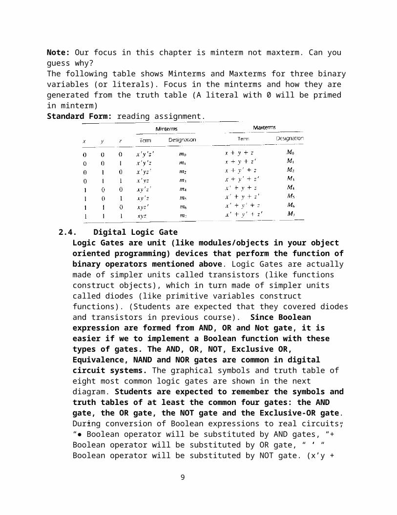
F = a’bc + b + c’ + a’b’ Canonical form: it is a Boolean expression form that one can directly derive from a truth table. Its unique characteristic is that each term contains one variable (literal).In a canonical form a term can be minterm or maxterm. Minterm: is an expression resulted when all possible inputs variables are combined with an AND binary operator (which finally resulted in an AND gate during circuit realization). A literal with 0 will be primed.Maxterm: is an expression resulted when all possible inputs variable are combined with an OR binary operator (which finally resulted in an OR gate during circuit realization). A literal with 1 will be primed.Note: Our focus in this chapter is minterm not maxterm. Can you guess why?The following table shows Minterms and Maxterms for three binary variables (or literals). Focus in the minterms and how they are generated from the truth table (A literal with 0 will be primed in minterm)Standard Form: reading assignment.
6

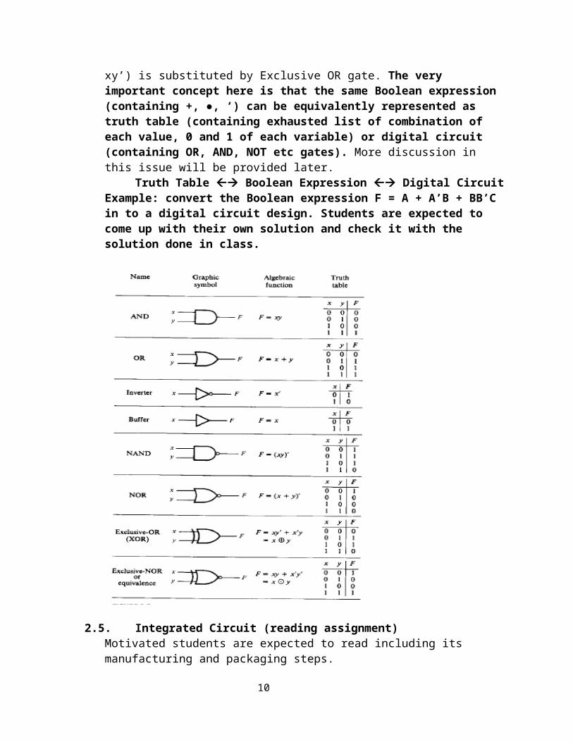
2.4. Digital Logic GateLogic Gates are unit (like modules/objects in your object oriented programming) devices that perform the function of binary operators mentioned above. Logic Gates are actually made of simpler units called transistors (like functions construct objects), which in turn made of simpler units called diodes (like primitive variables construct functions). (Students are expected that they covered diodes and transistors in previous course). Since Boolean expression are formed from AND, OR and Not gate, it is easier if we to implement a Boolean function with these types of gates. The AND, OR, NOT, Exclusive OR, Equivalence, NAND and NOR gates are common in digital circuit systems. The graphical symbols and truth table of eight most common logic gates are shown in the next diagram. Students are expected to remember the symbols and truth tables of at least the common four gates: the AND gate, the OR gate, the NOT gate and the Exclusive-OR gate. During conversion of Boolean expressions to real circuits, “●”Boolean operator will be substituted by AND gates, “+” Boolean operator will be substituted by OR gate, “ ‘ “ Boolean operator will be substituted by NOT gate. (x’y + xy’) is substituted by Exclusive OR gate. The very important concept here is that the same Boolean expression (containing +, ●, ‘) can be equivalently represented as truth table (containing exhausted list of combination of each value, 0 and 1 of each variable) or digital circuit (containing OR, AND, NOT etc gates). More discussion in this issue will be provided later.
Truth Table Boolean Expression Digital CircuitExample: convert the Boolean expression F = A + A’B + BB’C in to a digital circuit design. Students are expected to come up with their own solution and check it with the solution done in class.
7

2.5. Integrated Circuit (reading assignment)Motivated students are expected to read including its manufacturing and packaging steps.
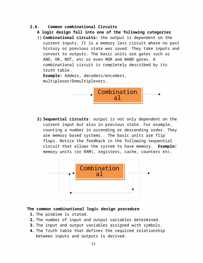
2.6. Common combinational CircuitsA logic design fall into one of the following categories1) Combinational circuits: the output is dependent on the current inputs. It is a
memory less circuit where no past history or previous state was saved. They take inputs and convert to outputs. The basic units are gates such as AND, OR, NOT, etc or even NOR and NAND gates. A combinational circuit is completely described by its truth table.Example: Adders, decoders/encoders, multiplexer/Demultiplexers.
8
CombinationalCircuit
2) Sequential circuits: output is not only dependent on the current input but also in previous state. For example, counting a number in ascending or descending order. They are memory based systems. The basic units are flip flops. Notice the feedback in the following sequential circuit that allows the system to have memory. Example: memory units (or RAM), registers, cache, counters etc.
The common combinational logic design procedure1. The problem is stated.2. The number of input and output variables determined.3. The input and output variables assigned with symbols.4. The Truth table that defines the required relationship between inputs and outputs is
derived.5. The simplified Boolean function for each output is obtained.6. The logic diagram is drawn. (or realized)
All the above steps were discussed in the previous section, now it is time to mix them and come up with a general picture.
2.6.1. Binary Adders Handles binary addition (this means they also deal with Subtraction with proper signed
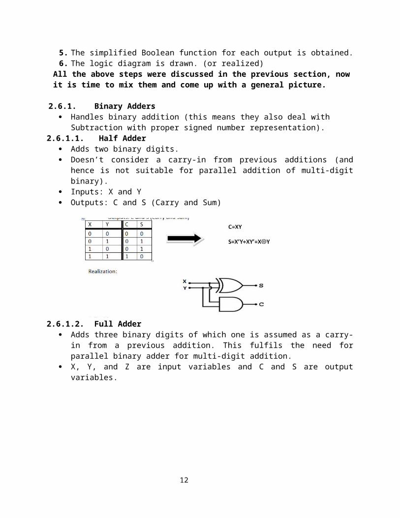
number representation).2.6.1.1. Half Adder
Adds two binary digits. Doesn’t consider a carry-in from previous additions (and hence is not suitable for
parallel addition of multi-digit binary). Inputs: X and Y Outputs: C and S (Carry and Sum)
9
CombinationalCircuit
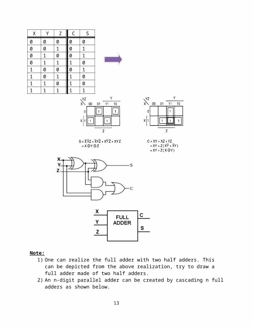
2.6.1.2. Full Adder Adds three binary digits of which one is assumed as a carry-in from a previous addition.
This fulfils the need for parallel binary adder for multi-digit addition. X, Y, and Z are input variables and C and S are output variables.
10
X Y Z C S0 0 0 0 00 0 1 0 10 1 0 0 1
0 1 1 1 01 0 0 0 11 0 1 1 01 1 0 1 01 1 1 1 1
Note:1) One can realize the full adder with two half adders. This can be depicted from the above
realization, try to draw a full adder made of two half adders.2) An n-digit parallel adder can be created by cascading n full adders as shown below.
AnAn-1……A2A1A0
+ BnBn-1…….B2B1B0
CoutSnSn-1……..S2S1S0
2.6.2. Encoders and DecodersEncoder: An encoder is a device used to change a signal or data into a code. The code may serve any of a number of purposes such as compressing information for transmission or storage, encrypting or adding redundancies to the input code, or translating from one code to another. In digital electronics this would mean that a decoder is a multiple-input, multiple-output logic circuit (2n to n).
Decoder: A decoder is a device which does the reverse of an encoder, undoing the encoding so that the original information can be retrieved. The same method used to encode is usually just reversed in order to decode. In digital electronics this would mean that a decoder is a multiple-input, multiple-output logic circuit (n to 2n).
11
Our discussion shall focus on Decoders as they can be used as a building block to realize any Boolean expression.
A Decoder is a combinational circuit that converts binary information from n input lines to a maximum of 2n unique output lines. If the n-bit decoded information has ‘unused’ components or don’t care conditions, the unique output shall be less than 2n.
To demonstrate, let’s consider a 3x8 Decoder. Inputs X, Y, Z Output D0, D1, D2, D3, D4, D5, D6, D7
As you may notice from the basic property of the decoder, each output corresponds to a unique minterm. Therefore, Decoders are also called Minterm Generators. For each of the input combinations, exactly one output is true. Each output equation contains all of the input variables. These properties hold for all sizes of decoders.
As the say goes, any logic circuit is fully explained by a truth table and the truth table can be expressed as a sum of minterms. Therefore, a decoder can serve as a kind of universal device to deploy any Boolean function with the help of one external OR gate (one OR gate per output function). The only pre-requisite is to have the Boolean expression in Canonical form as a Sum of Minterms (SOM).
Examples:1) Deploy the full adder circuit using a 3x8 decoder.
Solution: From our previous discussion of adders, use decoder to implement sum (S) and carry (C) of a full adder. Decoder and two or gates (one for each output) can be used in a straight forward manner.
12
D0=X ' Y ' Z 'D1=X ' Y ' ZD2=X ' YZ 'D3=X ' YZD4=XY ' Z 'D5=XY ' ZD6=XYZ 'D7=XYZ
2) Realize f (a ,b , c , d )=a ' b+abcd+d+c '+b ' cd
using a decoder. (Class work. Hint: First you need to convert the expression in to Canonical form and then utilize a 4 x 16 decoder to realize the function).
3) Design a BCD to Decimal converter. (Class work. Hint: Inputs a, b, c, d Outputs 0,1,2,3,4,5,6,7,8,9. Use a 4x 16 decoder and take output from the minterms and leave the don’t care conditions disconnected). You should have the knowledge of K-Map to simplify Boolean expression to solve this problem.
2.6.3. Multiplexers/Demultiplexers Multiplexing implies channel sharing; that means transmitting a large number of
information sources over a smaller number of channels or lines. It quite often happens, in the design of large-scale digital systems, that a single line is
required to carry two or more different digital signals. (as an example: instead of having single path for each car, it is resource efficient to have a single wide path and letting all cars use it with traffic light – the multiplexer. Of course, only one signal at a time can be placed on the one line. What is required is a device that will allow us to select, at different instants, the signal we wish to place on this common line (like the traffic light). Such a circuit is referred to as a Multiplexer.
A digital multiplexer (mux) is a combinational circuit that selects binary information from one of many input lines and directs it to a single output line. The selection of the particular input line is controlled by a set of selector lines.
A 2n-to-1 multiplexer sends one of 2n input lines to a single output line. o A multiplexer has two sets of inputs:
2n data input lines n select lines, to pick one of the 2n data inputs
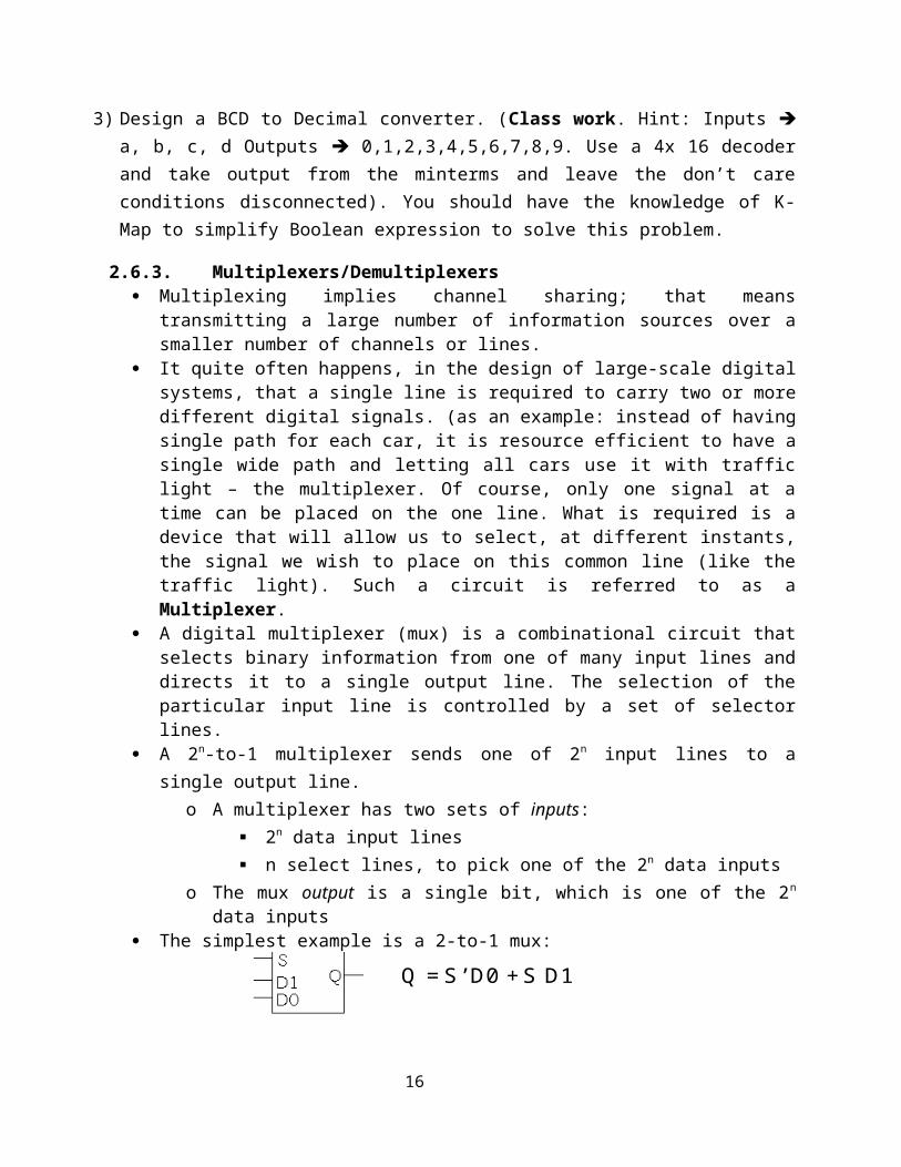
o The mux output is a single bit, which is one of the 2n data inputs The simplest example is a 2-to-1 mux:
Q = S’ D0 + S D1
o The select bit S controls which of the data bits D0-D1 is chosen: If S=0, then D0 is the output (Q=D0). If S=1, then D1 is the output (Q=D1).
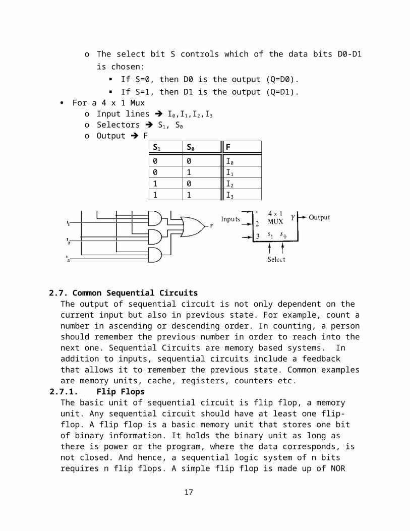
For a 4 x 1 Muxo Input lines I0,I1,I2,I3
o Selectors S1, S0
o Output FS1 S0 F0 0 I0
13

0 1 I1
1 0 I2
1 1 I3
2.7. Common Sequential CircuitsThe output of sequential circuit is not only dependent on the current input but also in previous state. For example, count a number in ascending or descending order. In counting, a person should remember the previous number in order to reach into the next one. Sequential Circuits are memory based systems. In addition to inputs, sequential circuits include a feedback that allows it to remember the previous state. Common examples are memory units, cache, registers, counters etc.
2.7.1. Flip FlopsThe basic unit of sequential circuit is flip flop, a memory unit. Any sequential circuit should have at least one flip-flop. A flip flop is a basic memory unit that stores one bit of binary information. It holds the binary unit as long as there is power or the program, where the data corresponds, is not closed. And hence, a sequential logic system of n bits requires n flip flops. A simple flip flop is made up of NOR gates or NAND gates. The following is the basic diagram of flip flop. It has two inputs, Reset (R) and Set (S). It has two outputs, Q and Q’. Q is considered the normal (functional) output of the flip flop that determines its states. Q’ is negated output of Q. In flip flops, Q should never be equal with Q’. As can be seen from the following truth table, when S=1, R=0 then Q=1. When S=0, R=1 then Q=0. When S=0 and R=0 then the flip flop keeps its state i.e., Q keeps what it has. When S=1, R=1 then Q=0 and Q’=0 which is indeterminate. Can you try to determine the above cases by tracing in flip flop circuit?
2.7.1.1. Synchronous RS Flip Flop.
14

Synchronous RS Flip flops are the most common types of flip flops. To make the flip flop synchronous, additional control circuitry is put to the left of the flip flop. This will make the flip flop to respond to inputs when only the clock pulse (CP) is on. Such circuits are known as synchronous. The behavior of RS flip flop is as follow: When S=1, R=0 then Q=1. When S=0, R=1 then Q=0. When S=0 and R=0 then Q keeps what it has. S=1, R=1 then Q=0 and Q’=1 which is indeterminate. Always remember that the state of the flip flop is specified by the value of Q. The graphical symbol of RS flip flop is as shown below. It takes two inputs S and R and changes the state of the flip flop (that means Q) accordingly only when the clock pulse (C) is on. Other flip flops are constructed by modifying RS flip flop in order to make it more suitable for a specific purpose. Some of them are D-Flip flop, JK flip flop, T flip flop. The graphical symbol of RS flip flops is as follow.
2.7.1.2. D Flip FlopD Flip flops are known as Data flip flops. The logic diagram for D flip flop is shown in the next diagram. It is a single input flip flop. The input to D flip flop is labeled as D. The characteristic of D flip flop is as follow: When D=0 then Q=0. When D=1, then Q=1. i.e., the state of D flip flop is the same as the D input. What do you think the use of D flip flops? As can be seen from its characteristic table D flip flops are used to store data which makes them suitable for memory devices like registers and cache and RAM.
15
2.7.1.3. JK Flip FlopJK flip flop is designed to cancel the indeterminate nature of RS flip flop. J is equivalent with S and K is equivalent with R in RS flip flop. It has similar behavior with RS flip flop but the JK flip flop toggles (complement) the state of flip flop when J=1 and R=1. Note that the RS flip flop is indeterminate for this case. The characteristic of JK flip flop is as follow: when J=0 and K=0, then the flip flop keeps what it has. When J=1 and K=0, then the flip flop is set to 1 i.e., Q=1. When J=0 and K=1, then the flip flop is set to 0. When J=1 and K=1, then the flip flop toggles (converts or complements) its state i.e., the value of Q is toggled. Note that this case gives indeterminate in RS flip flop.
2.7.1.4. T flip flopT flip flop is a single input version of JK flip flop, it has the capability to toggle, or complement its state. The input to T flip flop is labeled as T. The characteristic of T flip flop is as follow: when T=0, then it keeps its current state (Q). When T=1 its current state
16
is toggled. What do you think the use of T flip flop? It is used in binary counters which in turn has applications in design of control unit of computers.
2.7.2. Memory Units RegistersMemory units are made up of D-flip flops. To write 1 to the flip flop D is set to 1 whereas to write 0 to the flip flop D is set to 0. An n bit memory is made up of n D flip flops. For example: an 8 bit RAM (register) contains 8 memory units made up of 8 D-flip flops in which data can be written to it by setting the D inputs or read by reading the Q value. This process is known as memory write/read operation. More discussion about Memory will be given in later chapters.
2.7.3. Binary CountersCounters are made up of T flip flops. To increment the counter value, the state of the appropriate flip flop/flip flops is changed by setting its T inputs. For example: for a counter that counts from 0 up to 3, how many flip flops are needed? Two flip flops. When the state of the two flip flop is 00 (i.e., it is at state 0), when the state of the two flip flop is 01 (i.e., it is at state 1), when the state of the two flip flop is 10 (i.e., it is at state 2), and finally When the state of the two flip flop is 11 (i.e., it is at state 3),. Assume the current state of the flip flop is at state 10 (which is at state 2), then to increment the counter to 3; the T input to the first flip flop is set at 0 (keep what you have i.e., at state 0), the T- input to the second flip flop is set to 1 (toggle its state from 0 to 1). Now the state of the two flip flops is changed from 10 (which is 2) to state 11 (which is 3). This is just like counting from 2 to 3.
The design of sequential circuits is much wider than combinational circuits. It adds several concepts on top of combinational circuit design procedure. Any interested student can go deep in to the concept and welcomed to come up with any challenge to the instructor.
17