Embed Size (px)
Citation preview

INTRODUCTION TO ACTIVE AND PASSIVE ANALOG
FILTER DESIGN INCLUDING SOME INTERESTING AND
UNIQUE CONFIGURATIONS
Speaker:
Arthur Williams – Chief Scientist Telebyte Inc.
Thursday November 20th 2008

• Introduction • Basic Filter Polynomial types• Frequency and Impedance Scaling • Active Low-Pass Filters• Design of D-Element Active Low-Pass Filters• High-Pass Filters• Band-Pass Filters• Band-Reject Filters• High-Q Notch Filters• Q-Multiplier Active Band-Pass Filters• Some Useful Passive Filter Transformations• Attenuators• Power Splitters• Miscellaneous Circuits• Questions and Answers
TOPICS

Introduction
Generalized Passive Filter
)(
)()(
sD
sN
E
EsT
s
L ==
122
1)(
23 +++=
ssssT
N=3 ButterworthNormalized 3dB at 1 Rad/s
Pole Zero Plot on j-Omega Axis

Most Popular Filter Polynomial Types
ButterworthChebyshevLinear Phase Elliptic Function

Butterworth
The Butterworth approximation based on the assumpt ion that a flat response at zero frequency is more important than the respo nse at other frequencies.Normalized transfer function is an all-pole typeRoots all fall on a unit circle The attenuation is 3 dB at 1 rad/s.
Normalized Frequency Response
Roots on j-Omega Axis
N=5 Butterworth LPF and its Dual

Butterworth LC Element Values (Representative Table , Extensive tables in reference)
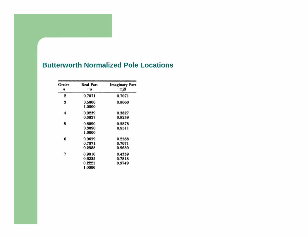
Butterworth Normalized Pole Locations
Chebyshev
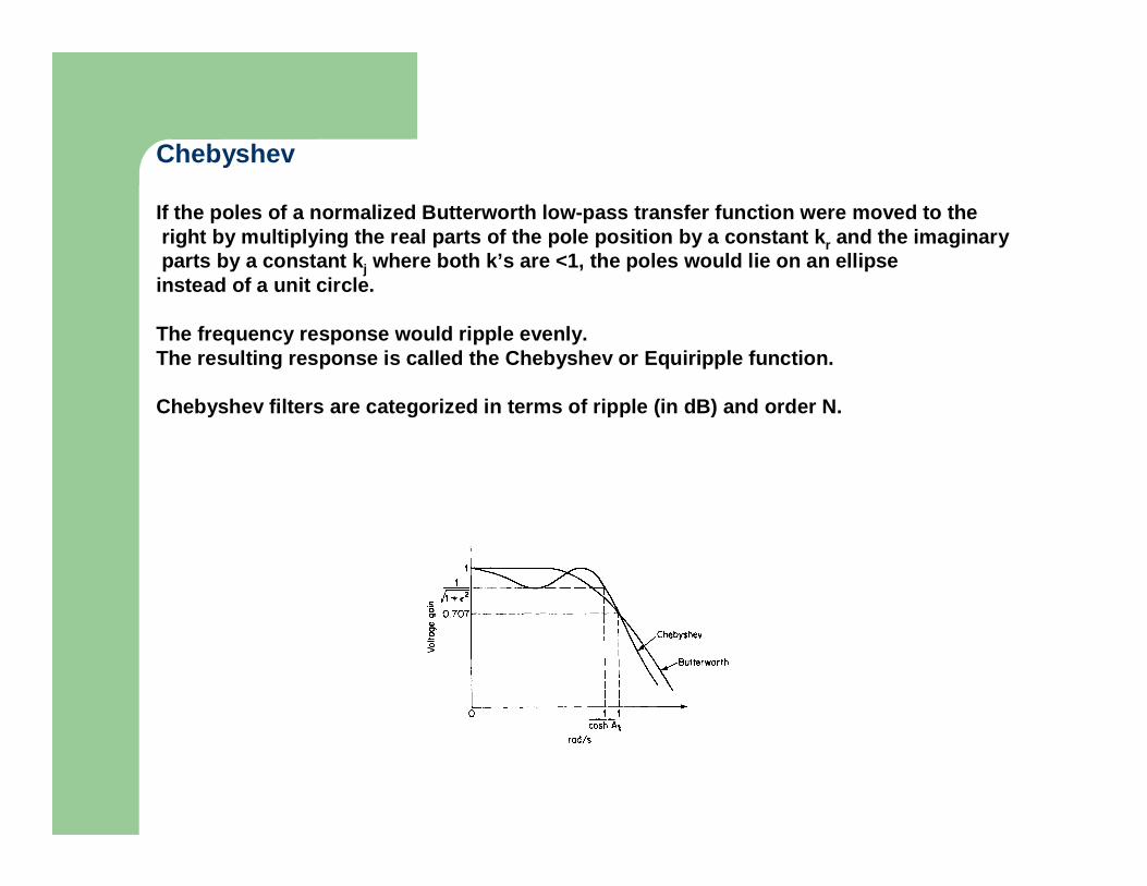
If the poles of a normalized Butterworth low-pass t ransfer function were moved to theright by multiplying the real parts of the pole pos ition by a constant kr and the imaginaryparts by a constant kj where both k’s are <1, the poles would lie on an ellipse instead of a unit circle.
The frequency response would ripple evenly. The resulting response is called the Chebyshev or Eq uiripple function.
Chebyshev filters are categorized in terms of ripple (in dB) and order N.

Chebyshev Low-Pass Filter

Linear Phase Low Pass Filters
Butterworth filters - good amplitude and transient characteristics
Chebyshev family of filters- increased selectivity but poor transient behavior Bessel transfer function - optimized to obtain a linear phase, i.e., a maximally flat delay
Frequency response- Much less selective than other filter types
The low-pass approximation to a constant delay can be expressed as the following general Bessel transfer function:
sssT
coshsinh
1)(
+=
sssT
coshsinh
1)(
+=

Linear Phase Low-Pass Filters
Other Linear Phase Filter Families– Gaussian– Gaussian to 6dB– Gaussian to 12dB– Linear Phase with Equiripple Error (0.05°and 0.5°)– Maximally Flat Delay with Chebyshev Stop-Band
Extensive tables are available in the reference

Effects of Non-Linear Phase
Amplitude and Phase Response ofN=3 Butterworth Low-Pass Filter
Group Delay of N=3 Butterworth Low-Pass Filter
Square Wave containing Fourier Seriesa) Equally delayed componentsb) Unequally delayed components

Elliptic Function
All filter types previously discussed are all-pole networks.Infinite rejection occurs only at the extremes of t he stop-band.Elliptic-function filters have zeros as well as pol es at finite frequencies.Introduction of transmission zeros allows the stee pest rate of descent theoretically possible for a given number of poles. However the highly non-linear phase response results in poor transient performance.

Normalized Elliptic Function Low-Pass Filter
RdB = Ripple in dB up to cut-off (1 Rad/sec)Amin= Minimum Stop-Band Attenuation in dBΩS = Normalized Frequency (Rad/sec) to achieve A min (Steepness Factor)

Frequency and Impedance Scaling from Normalized Circuit
frequency reference existing
frequency reference desiredFSF =
Frequency Scaling
Normalized N ==== 3 Butterworth low-pass filter normalized to 1 rad/sec : (a) LC filter; ( b) active filter; (c) frequency response

Denormalized low-pass filter scaled to 1000Hz: (a) LC filter; ( b) active filter; (c) frequency response.
All Ls and Cs of the normalized Low-Pass filter are divided by 2 π FC where FC=1,000 Hz
Note Impractical Values

Impedance Scaling
A transfer function of a network remains unchanged if all impedances are multiplied (or divided) by the same factor.
This factor can be a fixed number or a variable, as long as every impedance element that appears in the transfer function is mu ltiplied (or divided) by the same factor.
Rule

Impedance scaling can be mathematically expressed as
R′′′′ ==== ZxR
L′′′′ ==== ZxL
C’=C
Z
Frequency and impedance scaling are normally combined into one step rather than performed sequentially. The denormalized values are then given by
L′ = ZxL/FSF
C’=Z x FSF
C
Impedance-scaled filters using Z=1K : (a) LC filter; ( b) active filter.

Bartlett’s Bisection Theorem
A passive network designed to operate between two e qual terminations canbe modified to work between two unequal termination s and still have the same Transfer Function (except for a constant multi plier) if the network is symmetrical. It can then be bisected and either half scaled in impedance.
Normalized N=3 LPF Bisected LPF
Right half impedance scaled by 1.5 Re-combined LPF
Resulting filter frequency and impedance scaled to 200Hz, 1K Source, 1.5K Load

Active Low-Pass Filters
Unity gain Active Low-Pass N=2 and N=3
12
1)(
22
21 ++=
sCsCCsT
N=2 Section
121
1)(
22
2
22+
β+α
α+
β+α
=
sssT
α=
11C 222
β+α
α=C
1
1)(
23 +++=
sCBsAsST
N=3 Section
A = C1C2C3
B = 2C3(C1 + C2)C = C2 + 3C3
Values can be frequency and Impedance scaled

Design of D-Element Active Low-Pass Filters and a Bi-Directional Impedance Converter for Resistive Loads
Generalized Impedance Converters (GIC)
Z11= Z2Z4
Z1Z3Z5By substituting RC combinations for Z1 through Z5a variety of impedances can be realized.

sCR1R3R5
R2
Z11=
If Z 4 consists of a capacitor having an impedance 1/sC where s=јωand all other elements are resistors, the driving point impedance becomes:
The impedance is proportional to frequency and is therefore identical to an inductor having an inductance of:
Note: If R1 and R2 and part of a digital potentiometer the value of L can be digitally programmable.
CR1R3R5
R2
L=
GIC Inductor Simulation

If both Z 1 and Z3 are capacitors C and Z2,Z4 and Z5 are resistors,the resulting driving point impedance becomes:
R5
s2C2R2R4Z11=
An impedance proportional to 1/s2 is called a D Element.
1s2DZ11= where: C2R2R4
R5D =
If we let C=1F,R2=R5=1 Ω and R4=R we get D=R so:
1s2RZ11=
If we let s=јω the result is a Frequency Dependant Negative Resistor FDNR
1-ω2RZ11=
D Element

D Element Circuit

A transfer function of a network remains unchanged if all impedances are multiplied (or divided) by the samefactor. This factor can be a fixed number or a variable, as long as every impedance element that appears in the transfer function is multiplied (or divided) by the same factor.
The 1/S transformation involves multiplying all impedances in a network by 1/S.
Rule
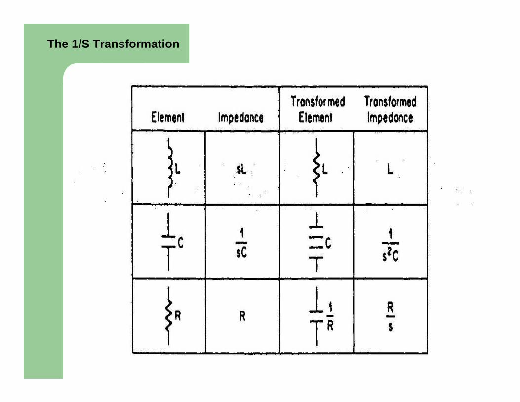
The 1/S Transformation

Normalized Low-Pass filter 1/S Transformation
Realization of D Element
Frequency and Impedance Scaled Final Circuit
Filter is Linear Phase ±0.5° Type
Design of Active Low-Pass filter with 3dB point at 400Hz using D Elements
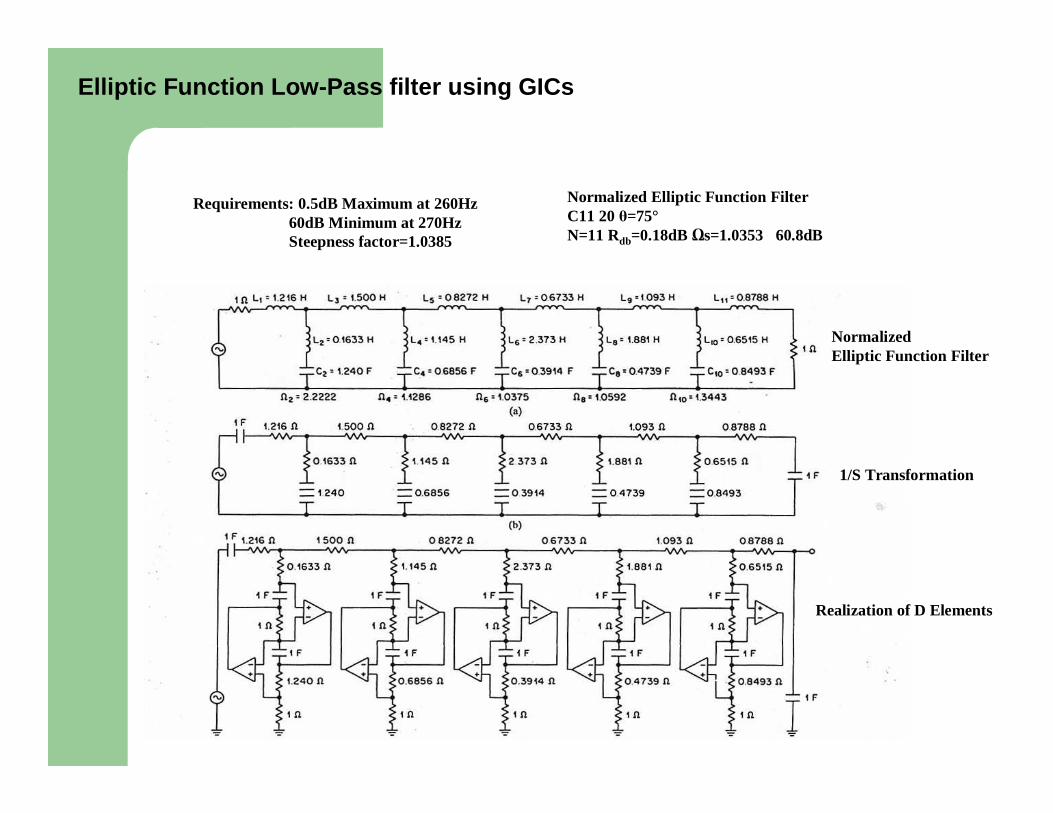
Requirements: 0.5dB Maximum at 260Hz60dB Minimum at 270HzSteepness factor=1.0385
Normalized Elliptic Function FilterC11 20 θ=75°N=11 Rdb=0.18dB Ωs=1.0353 60.8dB
NormalizedElliptic Function Filter
1/S Transformation
Realization of D Elements
Elliptic Function Low-Pass filter using GICs

Frequency and Impedance Scaled Final Circuit
Note: 1 meg termination resistor is needed to provide DC return path.

+ +
R RR R
Rs
Rs CGIC
CGIC
Value of R ArbitraryRs is source and load resistive terminationsCGIC is D Element Circuit Capacitive Terminations
Bi-Directional Impedance Converter for Matching D E lement Filters RequiringCapacitive Loads to Resistive Terminations

High–Pass Filters
Normalized Reciprocal Low-Pass High-Pass Relationsh ip

Passive High-Pass Filters
Low-Pass to High-Pass Transformation for Normalized Values
Lphp
1
LC =
LPhp
1
CL =
Replace Low-Pass Values by Reciprocal ComponentsThen frequency and impedance scale to desired cut-o ff

Active High-Pass Filters
To convert a normalized active low-pass filter into an active high-pass filter replace each resistor by a capacitor having t he reciprocal value and vice versa. The filter can then be scaled to the des ired cut-off and impedance level.
This conversion does not apply to feedback resistor s that determine an amplifiers gain which applies to some active configur ations.

Band-Pass Filters
Low-Pass to Band-Pass Transformation
This figure shows the relationship of a low-pass fi lter when transformed into a band-pass filter. The response at frequencies of the low-pass filter results in the same attenuation at corresponding bandwidths of the band-pass filter.

Band-Pass Filters
Band-Pass Transformation Procedure for LC Filters1) Design a low-pass filter having the desired Bandw idth of the band-pass filter and
impedance level.2) Resonate each inductor with a series capacitor and resonate each capacitor with
a parallel inductor. The resonant frequency should be the desi red center frequency of the band-pass filter.
Normalized N=3 Butterworth Low-Pass Filter Scaled to 3dB at 100Hz and 600-ohms
Resulting Band-Pass TransformationπFo=
1
2 LC

Wide Band Band-Pass Filters
Cascade of Low-Pass and High-Pass Example of Wide Band Band-Pass Filter
Effect of Interaction for Less Than an Octave of Se paration of Cut-Offs
To prevent impedance interaction between a passive low-pass filter and high-pass filter, a 3dB Attenuator between fil ters is helpful.

Band Reject Filters
This figure shows the relationship of a high-pass f ilter when transformed into a band-reject filter. The response at frequencies of the high-pass filter results in the same attenuation at corresponding bandwidths of the band-reject filter.

Band-Reject Filters
Band-Reject Transformation Procedure for LC Filters1) Design a high-pass filter having the desired Band width of the band-reject filter
and impedance level.2) Resonate each inductor with a parallel capacitor and resonate each capacitor
with a series inductor. The resonant frequency should be the desi red center frequency of the band-reject filter.
a) N=3 Normalized 1dB Chebyshev LPFb) Transformed HPFc) Frequency and Impedance Scaled HPF (500Hz BW)d) Resonate inductors and capacitorse) Resulting Response

This circuit is in the form of a bridge where a signal is applied across terminals’ 1 and 2 the output is measured across terminals’ 3 and 4. At ω=1all branches have equal impedances of 0.707 ∠∠∠∠-45°so a null occurs across the output.
High-Q Notch Filters

The circuit is redrawn in figure B in the form of a lattice. Circuit C is the Identical circuit shown as two lattices in parallel.

There is a theorem which states that any branch in series with both the ZA and ZB branches of a lattice can be extracted and placed outside the lattice. The branch is replaced by a short. This is shown in figure D above. The resulting circuit is known as a Twin-T. This circuit has a null at 1 radian for the normalized values shown.

To calculate values for this circuit pick a convenient value for C. Then
R1=1
2πfoC
The Twin-T has a Q (fo/BW3dB ) of only ¼ which is far from selective.
Note: R-source <<R1 R-load >>R1

Circuit A above illustrates bootstrapping a network β with a factor K. If β is a twin-T the resulting Q becomes:
Q =
If we select a positive K <1, and sufficiently close to 1, the circuit Q can be dramatically increased. The resulting circuit is shown in figure B.
14(1-K)
C L
C
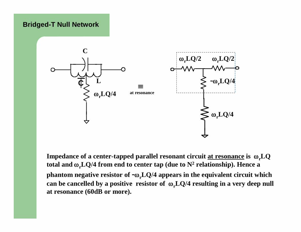
ωωωωrLQ/4≡≡≡≡
at resonance
ωωωωrLQ/2ωωωωrLQ/2
-ωωωωrLQ/4
ωωωωrLQ/4
Impedance of a center-tapped parallel resonant circuit at resonanceis ωωωωrLQtotal and ωωωωrLQ/4 from end to center tap (due to N2 relationship). Hence a
phantom negative resistor of -ωωωωrLQ/4 appears in the equivalent circuit which can be cancelled by a positive resistor of ωωωωrLQ/4 resulting in a very deep null at resonance (60dB or more).
Bridged-T Null Network

T(s)ΣIn
Out
1
+1
T(s) can be any band-pass circuit having properties of unity gain at fr,adjustable Q and adjustable fr.
Adjustable Q and Frequency Null Network

If T(s) in circuit A corresponds to a band-pass transfer function of:
The overall circuit transfer function becomes:
OutIn
The middle term of the denominator has been modified so the circuit Q is given by Q/(1-β) where
0<β <1. The Q can then be increased by the factor 1/(1-β) . Note that the circuit gain is increasedby the same factor.
Q Multiplier Active Bandpass Filters

A simple implementation of this circuit is shown in figure B.The design equations are:
First calculate β from β= 1 - Qr
Qeff
where Qeff is the overall circuit Q and Qr is the design Q of the bandpass section.
The component values can be computed from:
R1b=R1a
2Qr2-1
Where R and C can be conveniently chosen.

C1
C2
L
NC2
C2 N(N-1)
L
N2
N=1+CB
CA
Advantages :Reduces value of LAllows for parasitic capacity across inductor
CA
CB
LA
CA
N
CA(1-1/N)N2LA
Advantages:Increases value of L
N=1+C1
C2
Some Useful Passive Filter Transformations to Impro ve Realizability

This transformation can be used to reduce the value of a terminating resistorand yet maintain the narrow-band response.
Narrow Band Approximations
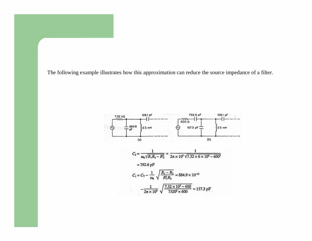
The following example illustrates how this approximation can reduce the source impedance of a filter.

An inductor can be used as an auto-transformer by adding a tap
Resonant circuit capacitor values can be reduced
Using the Tapped Inductor

Intermediate branches can be scaled in impedance
Leakage inductance can wreak havoc

Effect of leakage inductance can be minimized by splitting capacitors which adds additional poles
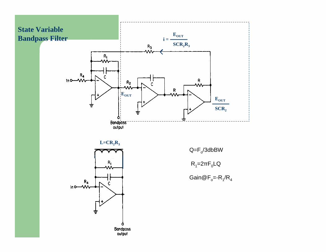
EOUTEOUT
SCR2
EOUT
SCR2R3
i =
EOUTEOUT
SCR2
EOUT
SCR2R3
i =L=CR2R3
State Variable Bandpass Filter
Q=Fo/3dbBW
R1=2πF0LQ
Gain@Fo=-R1/R4

Attenuators
Minimum Loss Resistive Pad For Impedance Matching
Rs 1-
RL
Rs
R1=
RL
R2=
1-RL
Rs
R1(R2+RL )
R2RL
+1Voltage Loss dB=20Log
10
Rs
RL
Power Loss dB= Voltage Loss dB - 10 Log10
R sR1
R2 RL
R s RL
R s>RL

Symmetrical T and π AttenuatorsdB/20
K= 10
For a Symmetrical T Attenuator
ZR1 =K+1
K-1 2 Z KR 3=
K 2- 1
R1
R3
Z Z
(a)
R3
R1/2 R1/2
R1/2 R1/2
Z Z
(b)
R1
Unbalanced Balanced

For a Symmetrical π Attenuator
(a) (b)
R1
R3
Z ZR1
Z Z
R3/2
R3/2
R1R1
ZR 1= K+1K-1
ZR 3=K2-12K
Unbalanced Balanced

T and PI Attenuators at 500-ohms Impedance LevelValues can be scaled to other impedances

Bridged T Attenuator
R1
RoRo
R2
RoRo
R0R1=
K-1R2 =R0 (K-1)
K= 10 dB/20 where
Only R 1 and R2 change to vary attenuation and they change inversel y
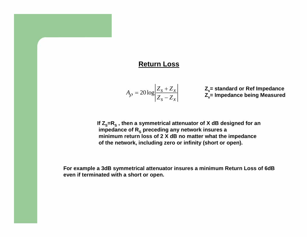
xs
xs
ZZ
ZZA
−
+= log20ρ
Return Loss
If ZS=RS , then a symmetrical attenuator of X dB designed fo r animpedance of R S preceding any network insures aminimum return loss of 2 X dB no matter what the im pedanceof the network, including zero or infinity (short o r open).
For example a 3dB symmetrical attenuator insures a minimum Return Loss of 6dBeven if terminated with a short or open.
Zs= standard or Ref ImpedanceZx= Impedance being Measured

Resistive Power Splitter
Port 1
Port 2
Port 3
Port K
R
R
R
R
N= total number of ports - 1 (N=K-1)
R 0R =N+1
N-1
where R 0 is the impedance at all ports.
Power Loss dB = 10 Log101
N2

Miscellaneous Circuits and Topics

Constant Delay High Pass Filter Delay of N=3 Butterworth High-Pass Filter3dB at 100Hz
Delay peaks near 3dB Cutoff and approaches zero at higher frequenciesNot acceptable if constant delay is desired in the Pass-Band

Solution
Constant DelayLow Pass Filter
Delay = T
All-PassDelay LineDelay = T
+
Low-Pass Filter has unity gain in stop-band
All-Pass Delay Line has unity gain
In pass-band of Low-Pass Filter signals are cancell ed in summer by subtraction
In stop-band of Low-Pass Filter the signal path is through the delay line

Simple Active Shunt Inductor
+1
R1
R2
C
L
Let R 2>>R1
L=R1R2C
πFQmax=
1
2 C R1R2
Qmax=12
R2
R1

All-Pass Delay Line Section
C
0.2432 F
1.605 F
1.605 H
1-Ohm 1-Ohm
Flat delay of 1.60 Sec within 1% to 1 Rad/S
π 2 F T total
1.6N =
Round off to nearest higher NUse N sections each scaled to delay of T total /NImpedance scale to practical values
Use high-Q Inductors to avoid dips at parallel resonant frequency

DualityAny ladder network has a dual which has the same tr ansfer function. In order to transform a network into its dual:• Inductors are transformed into capacitors and vice versa havingthe same element values (henrys into farads and vic e versa)
•Resistors are transformed into conductances ( ohms i nto mhos)•Open circuit becomes a short circuit and vice versa•Voltage sources become current sources and vice ver sa•Series branches become shunt branches and vice vers a•Elements in parallel become elements in series and vice versa
Note that the following table has schematics on bot h top and bottom which are duals of each other

Out of Band Impedance of Low-Pass and High-Pass Fil ters to Allow Combining
•The input and/or output impedance of a low-pass and high-pass filter is determined to a great extent by the last element.
•For example a low-pass filter having a series induc tor
at the load end has a rising impedance at that end i n the stop band (for rising frequencies).
•A high-pass filter having a series capacitor at the load end has a rising impedance In the stop band (for lower frequencies).
•This property allows the paralleling of low-pass an d high-pass filters with minimal interaction as long as the pass-bands don’t overlap. By selecting odd or even order filters and/or by using a circuits’ dual, the appropriate series
terminating element can be forced.

Balanced Series Inductors
Combined Shunt Inductorand Transformer
Low-Pass Filter3dB at 4KHz
High-Pass Filter3dB at 10KHz
Voice
DSL
Line
Simplified Low-Pass High-Pass Combining at Output
Practical Implementation in POTS Splitter
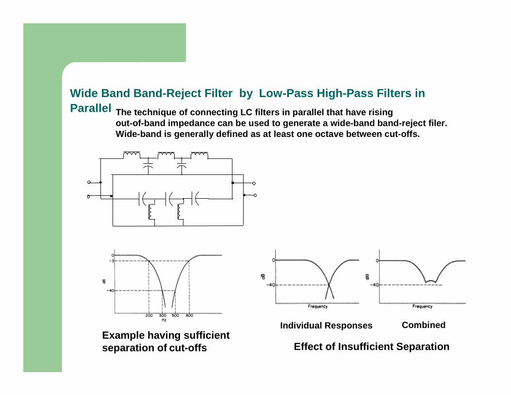
Wide Band Band-Reject Filter by Low-Pass High-Pass Filters in Parallel The technique of connecting LC filters in parallel that have rising
out-of-band impedance can be used to generate a wid e-band band-reject filer. Wide-band is generally defined as at least one octa ve between cut-offs.
Example having sufficient separation of cut-offs Effect of Insufficient Separation
Individual Responses Combined

REFERENCE:
Electronic Filter Design HandbookFourth Edition (McGraw-Hill Handbooks)Arthur Williams (Author) Fred J. Taylor (Author)
From Amazon http://www.amazon.com/
Or from McGraw Hillhttp://www.mhprofessional.com/Then enter Electronic Filter Design Handbook for search
This is the fourth edition of the Electronic Filter Design Handbook. This book was firstpublished in 1981. It was expanded in 1988 to inclu de five additional chapters on digital filters andupdated in 1995. This revised edition contains new material on both analog and digital filters. ACD-ROM has been included containing a number of pro grams which allow rapid design of analog filtersfrom input requirements without the tedious mathema tical computations normally encountered. The digital filter chapters are all integrated with a p rofusion of MATLAB examples.
Additional reference: “Filter Solutions” Software ht tp://www.filter-solutions.com/


![Introduction to KZ mechanism[File: Viewgraphs New/KibbleZurek/KZ- MechanismIntro.ai]](https://img.pdfslide.us/doc/110x75/5697bf9c1a28abf838c9308b/introduction-to-kz-mechanismfile-viewgraphs-newkibblezurekkz-mechanismintroai.jpg)


![Troop JLT Viewgraphs[1]](https://img.pdfslide.us/doc/110x75/577d2f881a28ab4e1eb1fb6a/troop-jlt-viewgraphs1.jpg)