Embed Size (px)
Citation preview

Layer-by-layer assembly of Zn(II) and Ni(II) 5,10,15,20-tetra(4-ethynylphenyl)porphyrin multilayers on Au using copper catalyzed azide-alkyne cycloaddition{
Alexandra Krawicz,a Joseph Palazzo,b Gwo-Ching Wangb and Peter H. Dinolfo*a
Received 9th March 2012, Accepted 7th June 2012
DOI: 10.1039/c2ra20440a
We have developed a versatile layer-by-layer (LbL) fabrication method to assemble porphyrin based
multilayer thin-films on electron-beam evaporated Au surfaces utilizing copper(I) catalyzed azide-
alkyne cycloaddition (CuAAC) as both a means of anchoring the films to the Au surface and coupling
the individual molecular layers together. The molecular based multilayer films are comprised of Zn(II)
and Ni(II) 5,10,15,20-tetra(4-ethynylphenyl)porphyrin and a bis-azido linker layer. Herein, we
describe the fabrication and characterization of multilayer films on Au surfaces modified with an
azido-terminated alkanethiol self assembled monolayer. The absorbance growth trends, as followed
by UV-vis absorption, show a consistent linear increase that extends over tens of bilayers. Multilayer
film thicknesses were obtained from spectroscopic ellipsometry, using a Cauchy model applied over
the transparent range, and resulted in a consistent linear growth trend. Optical constants, index of
refraction and extinction coefficients, were then determined using an oscillator model over the entire
visible region. The resulting extinction coefficients were consistent with those typical of Zn(II) and
Ni(II) porphyrin absorption spectra. The topology of the films and surface roughness was analyzed by
tapping mode atomic force microscopy (TM-AFM) and confirmed the continuous nature of the films.
X-Ray photoelectron spectroscopy (XPS) was consistent with the expected elemental composition of
the porphyrin based films assembled on Au surfaces. Additionally, XPS was used to examine the
utility of ethylenediaminetetraacetic acid disodium salt (Na2EDTA) as a Cu chelator to remove
adventitious catalyst following multilayer fabrication.
Introduction
The modification of electrode surfaces using molecularly ordered
thin films, with tunable electrochemical and photophysical
properties, has widespread applications in the field of molecular
electronics, and photovoltaics, among others.1–4 One of the most
common methods of adding functionality to electrode surfaces is
through the use of self assembled monolayers (SAMs).5 Another
method is the layer-by-layer (LbL) fabrication technique, which
can generate ordered thin films, composed of multiple building
blocks, efficiently and inexpensively.6 This methodology has the
potential to control the orientation and ordering of the films’
components at the molecular level through simple solution
deposition techniques. The LbL approach is a convenient and
precise technique, which allows for the facile engineering of
electronic, photophysical, and chemical properties into the
nanostructured films.7,8
LbL thin film formation can be accomplished by a series of
sequential self-limiting coupling reactions that each deposit a single
layer of material on the surface at a time. A wide variety of multilayer
thin films have been assembled on different substrate surfaces via this
technique using polymer, inorganic and molecular building blocks.
There exist a variety of interlayer coupling reactions which have been
explored as coupling techniques for the LbL assembly method.
Examples include electrostatically assembled polyelectrolytes,8
alpha-zirconium phosphate coupled dyes,9–16 Langmuir–Blodgett
films, palladium-pyridyl coordination,17–21 polymeric layers made
through siloxane polymerization,22–28 or various other organic
reactions.29–34
We have recently developed a molecular LbL thin film
fabrication methodology utilizing copper(I)-catalyzed azide-
alkyne cycloaddition (CuAAC) reactions as both a means to
link the layers together and attach them to oxide surfaces.35–37
This technique was used to assemble nanoscale multilayer films
of tetraphenyl-Zn(II)-porphyrins and perylenediimide building
blocks on several substrates, including SiO2, indium tin oxide
(ITO), quartz and glass. The resulting films showed reproducible
and linear growth trends for absorbance and thickness over tens
aDepartment of Chemistry and Chemical Biology, Rensselaer PolytechnicInstitute, 110 8th Street, Troy, NY, 12180, USA. E-mail: [email protected] of Physics, Applied Physics and Astronomy, RensselaerPolytechnic Institute, 110 8th Street, Troy, NY, 12180, USA{ Electronic Supplementary Information (ESI) available: experimentalprocedures, visible transmission and specular reflection, TM-AFMimages, and survey and high-resolution XPS spectra. See DOI:10.1039/c2ra20440a
RSC Advances Dynamic Article Links
Cite this: RSC Advances, 2012, 2, 7513–7522
www.rsc.org/advances PAPER
This journal is � The Royal Society of Chemistry 2012 RSC Adv., 2012, 2, 7513–7522 | 7513
Dow
nloa
ded
on 1
3 A
ugus
t 201
2Pu
blis
hed
on 1
3 Ju
ne 2
012
on h
ttp://
pubs
.rsc
.org
| do
i:10.
1039
/C2R
A20
440A
View Online / Journal Homepage / Table of Contents for this issue

of layers.35–37 Discovered in 2001 by Sharpless and coworkers38
and Meldal and coworkers,39 CuAAC has been popularized as a
rapid, facile, and robust cycloaddition reaction utilizing inex-
pensive Cu(I) catalyst. This simple reaction is tolerant of a
variety of conditions and other functional groups, and has been
used extensively as a surface modification technique on multiple
surfaces.40–45 While a few other groups have used this reaction to
fabricate triazole-linked polymer based multilayers,46–49 to our
knowledge we were the first to report the use of CuAAC to build
molecular multilayer films.35–37
In this report, we describe the extension of this LbL multilayer
fabrication method to include tetraphenylporphyrin building
blocks assembled on electron-beam (e-beam) evaporated Au
surfaces that will allow for the examination of charge transport
properties via electrochemical methods and scanning probe
microscopies.50 E-beam evaporated gold provides an ideal
surface for the growth of nanostructured thin films due to its
relatively smooth surface and ability to form high-quality mixed
azido-alkane SAMs required for CuAAC based multilayer
growth.40,41,51,52 Multilayer formation on Au electrode surfaces
opens up the possibility of additional characterization methods
for nanoscale thin films and provides a reproducible platform to
analyze electrochemical electron transfer rates.51 Since our initial
report of molecular LbL thin film fabrication on oxide surfaces,
others have used CuAAC for LbL generation of phenyl-triazole
based molecular wires on Au(111) electrodes.53
We have been particularly interested in the use of porphyrin
building blocks in the assembly of these films. The highly tunable
electrical and optical properties of porphyrins have led to their
use in a wide range of materials chemistry applications.54
Multilayer thin films assembled using porphyrin based molecular
building blocks could lead to a wide range of applications
including artificial photosynthetic processes,3,55,56 semiconduc-
tor sensitization,57–60 and catalysts,42,61–63 among others.64,65
Previously, porphyrin based molecular multilayer films have
been assembled in a LbL fashion using a variety of covalent and
non-covalent coupling methods including, transition metal
coordination,14–16,66–68 electrostatic interactions between electro-
lytes,69–71 and purely organic linkages.32–34
Herein, we describe the synthesis and characterization of
multilayer films of Zn(II) and Ni(II) 5,10,15,20-tetra(4-ethynyl-
phenyl)porphyrin (1 and 2 respectively) assembled by CuAAC
on e-beam evaporated Au surfaces. Multilayer growth was
monitored by UV-visible spectroscopy, observing an increase in
absorbance at the porphyrin Soret and Q-bands with each
additional porphyrin layer. Spectroscopic ellipsometry was used
to determine the film thickness and optical constants, which are
important to predict or understand the nonlinear optical
properties of these multilayers. The surface morphology was
explored by AFM, commonly employed in the analysis of films
composed of porphyrins and phthalocyanines,72 to obtain a
representative image of the topology and to inspect the integrity
and roughness of the film. X-Ray photoelectron spectroscopy
(XPS) was used to analyze the chemical composition, along with
determining the left over copper catalyst in the film structures.
Porous materials created via CuAAC often contain excess copper
ions, but several extraction methods have been employed to
remove the adventitious catalyst.73,74 XPS was used herein to
determine the amount of copper remaining in the Au supported
porphyrin multilayer films before and after treatment with
ethylenediaminetetraacetic acid disodium salt (Na2EDTA).
Results and discussion
Multilayer growth
Fig. 1 outlines our methodology for assembling molecular
multilayers using CuAAC reactivity. The process relies on two
sequential self-limiting CuAAC reactions of a multi-ethynyl
functionalized tetraphenylporphyrin (1 or 2) and a multi-azido
linker (3 or 4). The fabrication process begins with a mixed
azido-alkane SAM formed on an e-beam evaporated Au surface
to provide the initial attachment point. The azide-terminated
SAM is then reacted with the ethynyl functionalized porphyrin (1
or 2) under CuAAC conditions (step 1, Fig. 1). This step results
in a densely packed monolayer of porphyrin attached to the
SAM through 1,4-subsituted 1,2,3-triazole linkages and a surface
that is now terminated in acetylene groups. After a series of
solvent washes to remove unreacted starting material and
catalyst, another CuAAC reaction is performed on the surface
with a multi-azido linker creating an azide terminated surface
(step 2 in Fig. 1). The combination of steps 1 and 2 result in one
molecular bilayer added to the surface. The two self-limiting
reactions are then repeated sequentially to yield additional
molecular bilayers which are covalently attached to the surface
via 1,4-subsituted 1,2,3-triazoles.
Fig. 2 shows the visible absorption spectra taken throughout
the fabrication of a multilayer of 1 and 4 on a glass supported
20 nm thick, optically semi-transparent Au surface. With each
consecutive CuAAC reaction of 1 with the azide terminated
surface there was a consistent increase in absorbance for the
Soret peak at y440 nm. The refractive index of Au changes
dramatically over the visible region; n is y1.45 from 400–450
nm, but drops sharply to y0.13 in the range of 600–900 nm.75
This drastic difference in refractive index creates artifacts in the
absorbance and reflectance spectra of multilayers grown on Au.
In the region between 600–900 nm, the Fresnel equations predict
that a large percentage of incident light is reflected back from the
surface due to the significant difference in the refractive index
between water (n = 1.33), in which the sample is placed, and Au
(y0.13). As the multilayer is assembled on the surface, the
refractive index rises to that of the film (y1.5, vide infra)
resulting in less reflected light (greater transmission) and the
appearance of a negative absorption region. Within that
increased transmission range, the appearance of two Q-bands
associated with 1 can clearly be seen at 560 and 600 nm. Similar
absorptivity changes were observed when linker 3 was incorpo-
rated into the films (Figure S1{).
Multilayer fabrication was also followed using near-normal
specular reflection off of thicker Au surfaces (100 nm). Fig. 3
shows the Fresnel reflectivity for the visible region throughout
multilayer growth from 1 through 16 bilayers of 1 and 4. The
spectra consistently decrease in reflectivity as each bilayer is
added to the Au surface. The spectra show similar porphyrin
features as found in the transmission mode measurements (see
Fig. 2 above) with decreases in reflectivity at the Soret and
Q-band region. The bands are shifted towards longer wave-
lengths by approximately 10–20 nm due to complications from
the Kramers–Kronig effect. The complex index of refraction (n)
7514 | RSC Adv., 2012, 2, 7513–7522 This journal is � The Royal Society of Chemistry 2012
Dow
nloa
ded
on 1
3 A
ugus
t 201
2Pu
blis
hed
on 1
3 Ju
ne 2
012
on h
ttp://
pubs
.rsc
.org
| do
i:10.
1039
/C2R
A20
440A
View Online

is composed of the real refractive index (n) and the imaginary
part (ik) according to the Kramers–Kronig relationship (eqn (1)),
where k is the extinction coefficient of the film.76
n(l) = n(l) + ik(l) (1)
Due to the high optical density of the porphyrin based
multilayers, the reflectivity spectra of these samples show a first-
derivative like line shape, with increased reflectance on the high
energy side of the absorption features, as predicted by the
Kramers–Kronig effect.77 Similar trends in specular reflectivity
changes were observed for multilayers formed with 2 and 4
(Figure S2{).
Spectroscopic ellipsometry
Ellipsometry is a non-destructive surface analysis technique that
is capable of determining the thickness and optical properties of
nanoscale thin films. Spectroscopic ellipsometry measures the
change in phase (D) and amplitude (Y) of elliptically polarized
light reflected off of a substrate surface as a function of
wavelength (l). The data for D(l) and Y(l) are then fit to a
Fig. 1 Schematic representation of molecular LbL multilayer growth using CuAAC reactivity on Au surfaces.
Fig. 2 Top: UV-Vis spectra of multilayers of 1 and 4 assembled on an
azide-terminated SAM on optically transparent e-beam evaporated Au
(20 nm thickness). The absorption spectra for porphyrin layers are
shown. Bottom: Absorbance vs. the number of bilayers at the Soret and
Q-bands illustrate the linear dependence for multilayer growth.
Fig. 3 Specular reflectivity scans of 1 through 16 bilayers of 1 and 4 on
100 nm thick Au. Only porphyrin layer spectra are shown for clarity.
This journal is � The Royal Society of Chemistry 2012 RSC Adv., 2012, 2, 7513–7522 | 7515
Dow
nloa
ded
on 1
3 A
ugus
t 201
2Pu
blis
hed
on 1
3 Ju
ne 2
012
on h
ttp://
pubs
.rsc
.org
| do
i:10.
1039
/C2R
A20
440A
View Online
model describing the complex index of refraction (n) and
thickness of the material as described above in eqn (1) for the
Kramers–Kronig relationship.76 The porphyrin based films
described in this study have strong, localized absorptions in
the visible region due to the Soret and Q-band transitions, thus
somewhat complicating the analysis of the ellipsometry data.
Spectroscopic ellipsometry was employed throughout the
growth of multilayers on Au substrates to provide information
on both the thickness and optical constants of the thin films.
Fig. 4 shows the measured D(l) data in the range of 405–742 nm,
collected at a 65u angle of incidence, for multilayers of 1 and 4.
The D(l) parameters are particularly sensitive to thickness
changes of the material.78–80 As additional bilayer reactions are
performed on the Au surface, there is a consistent decrease in
D(l), especially in the region around 460 nm where the Soret
band of 1 is located. This is consistent with the increasing
multilayer thickness from 4 to 16 bilayers. Similar trends in D(l)
were observed during multilayer growth using the other
molecular components outlined in Fig. 1.
To calculate the thickness of the multilayer thin films, we
employed the Cauchy dispersion model (eqn (2)), over the non-
absorbing region (674–741 nm) of the porphyrin, to describe the
refractive index (n) as a function of the wavelength (l).80
n(l)~AzB
l2z
C
l4(2)
This methodology allows for the straightforward determina-
tion of film thickness, without additional fitting parameters
required to describe k(l) for the material. Ellipsometry has been
used to find the film thickness of other absorbing materials such
as porphyrins,32,81 phthalocyanines,55,72,82,83 LbL assembled
polypyridyl–PdCl2 films,21 and even CuAAC coupled dendri-
meric films49 using similar methods.
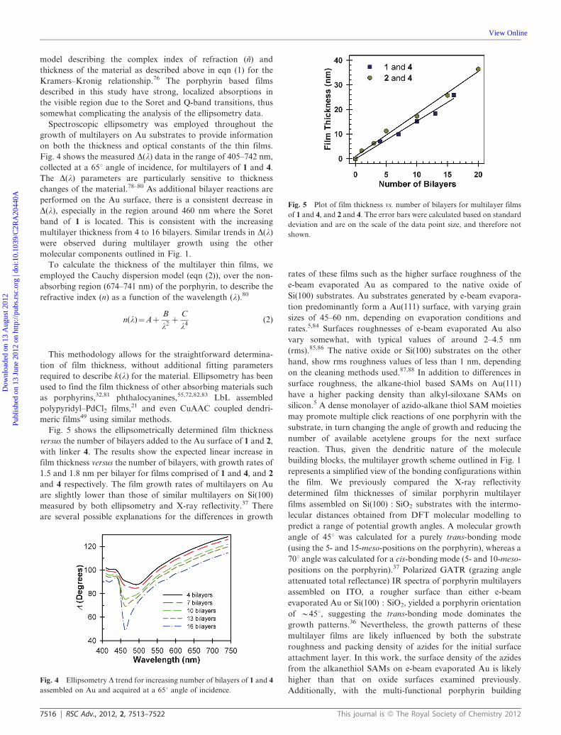
Fig. 5 shows the ellipsometrically determined film thickness
versus the number of bilayers added to the Au surface of 1 and 2,
with linker 4. The results show the expected linear increase in
film thickness versus the number of bilayers, with growth rates of
1.5 and 1.8 nm per bilayer for films comprised of 1 and 4, and 2
and 4 respectively. The film growth rates of multilayers on Au
are slightly lower than those of similar multilayers on Si(100)
measured by both ellipsometry and X-ray reflectivity.37 There
are several possible explanations for the differences in growth
rates of these films such as the higher surface roughness of the
e-beam evaporated Au as compared to the native oxide of
Si(100) substrates. Au substrates generated by e-beam evapora-
tion predominantly form a Au(111) surface, with varying grain
sizes of 45–60 nm, depending on evaporation conditions and
rates.5,84 Surfaces roughnesses of e-beam evaporated Au also
vary somewhat, with typical values of around 2–4.5 nm
(rms).85,86 The native oxide or Si(100) substrates on the other
hand, show rms roughness values of less than 1 nm, depending
on the cleaning methods used.87,88 In addition to differences in
surface roughness, the alkane-thiol based SAMs on Au(111)
have a higher packing density than alkyl-siloxane SAMs on
silicon.5 A dense monolayer of azido-alkane thiol SAM moieties
may promote multiple click reactions of one porphyrin with the
substrate, in turn changing the angle of growth and reducing the
number of available acetylene groups for the next surface
reaction. Thus, given the dendritic nature of the molecule
building blocks, the multilayer growth scheme outlined in Fig. 1
represents a simplified view of the bonding configurations within
the film. We previously compared the X-ray reflectivity
determined film thicknesses of similar porphyrin multilayer
films assembled on Si(100) : SiO2 substrates with the intermo-
lecular distances obtained from DFT molecular modelling to
predict a range of potential growth angles. A molecular growth
angle of 45u was calculated for a purely trans-bonding mode
(using the 5- and 15-meso-positions on the porphyrin), whereas a
70u angle was calculated for a cis-bonding mode (5- and 10-meso-
positions on the porphyrin).37 Polarized GATR (grazing angle
attenuated total reflectance) IR spectra of porphyrin multilayers
assembled on ITO, a rougher surface than either e-beam
evaporated Au or Si(100) : SiO2, yielded a porphyrin orientation
of y45u, suggesting the trans-bonding mode dominates the
growth patterns.36 Nevertheless, the growth patterns of these
multilayer films are likely influenced by both the substrate
roughness and packing density of azides for the initial surface
attachment layer. In this work, the surface density of the azides
from the alkanethiol SAMs on e-beam evaporated Au is likely
higher than that on oxide surfaces examined previously.
Additionally, with the multi-functional porphyrin building
Fig. 4 Ellipsometry D trend for increasing number of bilayers of 1 and 4
assembled on Au and acquired at a 65u angle of incidence.
Fig. 5 Plot of film thickness vs. number of bilayers for multilayer films
of 1 and 4, and 2 and 4. The error bars were calculated based on standard
deviation and are on the scale of the data point size, and therefore not
shown.
7516 | RSC Adv., 2012, 2, 7513–7522 This journal is � The Royal Society of Chemistry 2012
Dow
nloa
ded
on 1
3 A
ugus
t 201
2Pu
blis
hed
on 1
3 Ju
ne 2
012
on h
ttp://
pubs
.rsc
.org
| do
i:10.
1039
/C2R
A20
440A
View Online

blocks employed, it is possible that cross-linking can occur
within the multilayer structure, leading to a combination of
binding motifs present within the film.
Optical constants have also been obtained ellipsometrically for
absorbing films, containing porphyrins and phthalocyanines, by
modeling the dielectric functions of the material with an
oscillator model covering the full spectral range.72,82,89 These
methods typically use a fixed film thickness obtained from
Cauchy modeling in the transparent region, or other methods.89
We performed a full spectroscopic ellipsometry analysis of the
thicker multilayer structures. The upper plots in Fig. 6 show
representative ellipsometry data (D(l) and Y(l)) and fits for the
range of 410.0 to 741.5 nm (44 data points) for multilayers of 1
and 4, and 2 and 4 on Au(111) surfaces. The resulting model for
D(l) and Y(l), shown as solid lines, is in excellent agreement
with the measured data.
The bottom plots show the resulting n(l) and k(l) profiles for
the multilayer films as derived from the modeled dielectric
constants. As can be observed in the lower plots of Fig. 6, the
k(l) profiles closely match those of the absorption profile obtained
from UV-vis spectroscopy for the porphyrin multilayers
assembled on transparent Au (see Fig. 2). The multilayers
containing 1 (left plots) show a Soret absorbance feature at
435 nm and Q-bands at 560 and 610 nm. These are red-shifted
relative to the solution spectra of 1 due to aggregation effects within
the film.35–37 The k(l) profile for multilayers containing 2 display
Soret and Q-band features at 410 and 530 nm, which are closer to
those of the solution spectra of 2. Additionally, the n(l) spectrum of
both porphyrin based multilayers matches that of the specular
reflectivity assembled on opaque Au(111) substrates (see Fig. 3 and
S2{). The refractive index (n) for the porphyrin multilayer films is in
the range of 1.4–1.5 for films of 1 and 4, and 1.45–1.55 for films of 2
and 4 in the non-resonant region (674–741.5 nm).
Although optical constants for phthalocyanine are more
commonly reported in the literature than for porphyrin films,
the n(l) spectrum of vacuum evaporated thin films of free base
porphyrin was reported to be between 1.2–1.4 (in the range of 4–
12 eV) with prominent features between 0.5–4eV.90 Additionally,
the k(l) profile had prominent features that reflected the UV-vis
absorption profile.90 The literature value of the extinction
coefficient for phthalocyanine films from spectroscopic ellipso-
metry also shows agreement with the absorption spectra and the
refractive index range is comparable to our porphyrin multi-
layers.91 Others have reported refractive index values for
phthalocyanine containing films in the range of 1.6–1.8 in the
nonresonant region of the visible spectrum.72
Fig. 6 Spectroscopic ellipsometry data (410.0 to 741.5 nm, 44 data points) and fitting results for multilayers of 1 and 4 (left panels, a–c) and 2 and 4
(right panels, d–f). The top and middle panels show the D and Y data (open symbols) and fits (solid lines) collected at an incident angle of 55, 60, 65, 70,
and 75u. The bottom panel shows the resulting optical constants for the multilayer films as determined by the oscillator model. The index of refraction
(n) is shown as a dashed red line and the extinction coefficient (k) as a solid blue line.
This journal is � The Royal Society of Chemistry 2012 RSC Adv., 2012, 2, 7513–7522 | 7517
Dow
nloa
ded
on 1
3 A
ugus
t 201
2Pu
blis
hed
on 1
3 Ju
ne 2
012
on h
ttp://
pubs
.rsc
.org
| do
i:10.
1039
/C2R
A20
440A
View Online

Tapping mode atomic force microscopy
Topography and surface roughness was analyzed with tapping
mode atomic force microscopy (TM-AFM) to confirm the
continuity and integrity of the film on the Au surfaces. Fig. 7
shows representative 1 mm 6 1 mm topography and amplitude
TM-AFM images for multilayers comprised of 2 and 4. The
amplitude images remove long-range variations and offsets, and
therefore are sometimes better for visualization of the surface
features.92 The values of root mean squared roughness (rms) for
the images in Fig. 7 are 2.1, 2.6 and 3.7 nm for 1, 10 and 20 bilayers
of 2 and 4, respectively. The TM-AFM images of the multilayers
of 1 and 4 are shown in Fig. S3{ and yielded rms values of 2.5, 2.1
and 3.8 for 4, 10 and 16 bilayers, respectively. Larger area scans of
10 mm 6 10 mm show continuous multilayer films and comparable
roughness values. There was no apparent surface damage after
repeated TM-AFM scans of the same area. The rms tends to
increase slightly as more layers are deposited, and is similar to
observations made for similar multilayers on silicon.37 The
roughness of the multilayer films is similar to that of the
underlying Au surface,85,86 suggesting that the film morphology
is templated somewhat by the underlying substrate.55
X-Ray photoelectron spectroscopy and copper removal methods
We employed X-ray photoelectron spectroscopy (XPS) to
confirm the surface attachment of the molecular components
and to estimate the amount of copper catalyst remaining in the
multilayer film. XPS is a common surface characterization
technique and has been used to analyze porphyrin films on
gold93 and other surfaces.32 Copper contamination was reported
by others who used CuAAC reactivity in the assembly of
LbL films and the functionalization of acetylene-terminated
monolayers.94 In some cases, the remaining copper catalyst was
removed by EDTA37 or other chelating agents.73
A representative XPS spectrum of a multilayer film consisting
of 2 bilayers of 1 and 4 before and after treatment with 0.01 M
Na2EDTA is shown in Fig. 8. (The XPS spectra for multilayers
of 1 and 3 are shown in Fig. S4.{) The spectrum shows all of the
expected atomic peaks for the empirical formula for the 1 and 4
multilayer structure. High resolution spectra of the N 1s peak
(Fig. S5{) display a broadened spectrum with binding energies
around 398–401 eV due to multiple types of nitrogen atoms
in the film, including the porphyrin ring, 1,2,3-triazole and
unreacted azide groups. Additionally, high-resolution spectra for
the Zn 2p1/2 and 2p3/2 (Fig. S6{) show peaks at binding energies
of 1044.6 ¡ 0.2 and 1021.7 ¡ 0.2 eV, respectively, in close
agreement with values previously reported for other Zn
porphyrins.4,32,95–99
Table 1 contains atomic composition data taken from XPS
spectra for 2 bilayers of 1 and 3 and 1 and 4, before and after
treatment with Na2EDTA(aq). Table 1 also includes a compar-
ison of the atomic ratios of Cu and N to that of Zn. It is clear
from the XPS elemental spectra that some copper catalyst
remains in the film following multilayer fabrication. In an
attempt to remove the left over Cu, we exposed each film to a
0.01 M Na2EDTA solution (pH = 4.8) following each CuAAC
reaction. As can be seen in Table 1, the percentage of Zn did not
change significantly after Na2EDTA(aq) treatment and stayed
within 0.9 to 1.2%. Meanwhile, the amount of Cu detected was
between 1–2.8 times higher with respect to Zn before
Na2EDTA(aq) treatment, but dropped to a ratio of 1–1.3
afterwards.
While Na2EDTA was not effective in removing all of the
CuAAC catalyst from the multilayer films, XPS was able to
Fig. 7 TM-AFM images of 1 (left), 10 (middle) and 20 (right) bilayers of multilayers based on 2 and 4. The upper images are topography AFM height
profiles and the lower are amplitude scans, a pseudoderivative of the topography data to emphasize the structural characteristics. All TM-AFM images
areas are 1 mm 6 1 mm.
7518 | RSC Adv., 2012, 2, 7513–7522 This journal is � The Royal Society of Chemistry 2012
Dow
nloa
ded
on 1
3 A
ugus
t 201
2Pu
blis
hed
on 1
3 Ju
ne 2
012
on h
ttp://
pubs
.rsc
.org
| do
i:10.
1039
/C2R
A20
440A
View Online

provide information about the nature of the remaining Cu
species. Fig. 9 shows the high-resolution spectra of the Cu 2p3/2
peaks for multilayers of 1 and 3 and 1 and 4 before and after
treatment with Na2EDTA(aq). The high-resolution XPS spectra
show a broad set of Cu 2p1/2 and 2p3/2 peaks, consistent with
multiple Cu species. Deconvolution of the spectra, shown in
Fig. S7{, reveal the presence of both Cu(I) and Cu(II) species at
binding energies of 932.4 ¡ 0.2 and 934.4 ¡ 0.2 eV,
respectively.100–102 Table 2 contains a comparison of the
Cu(II)/Cu(I) ratios, from deconvolution of the Cu 2p3/2 peaks,
before and after Na2EDTA(aq) treatment. Following treatment
with Na2EDTA, the XPS data shows a marked decrease in the
Cu(II) 2p3/2 peaks relative to Cu(I) (see the ESI{), and the
disappearance of the Cu(II) satellite peaks at approximate
binding energies of 944 and 962 eV. This data suggests that
Na2EDTA(aq) is more effective at removing Cu(II) species than
Cu(I) from the multilayer films.
We previously found that untreated multilayer films of 1 and 3
assembled on the native oxide of Si(100) substrates had a
Cu : Zn ratio of 1.36 : 1, whereas films of 1 and 4 had a
significantly lower ratio, 0.16 : 1.37 We proposed that the higher
amounts of Cu in the multilayers with linker 4 may be a result of
the two sulfonates compared to 3 which does not contain any
anionic groups. The Na+ peak in the high-resolution XPS spectra
was relatively small for the expected atomic composition of the
multilayers grown with 4, suggesting that Cu ions exchanged
with the sulfonate cations of 4. The comparable amount of Cu
present in the multilayers containing linker 3 suggests that there
Fig. 8 XPS spectra of multilayers of 1 and 4 before (green dashed line) and after (red solid line) treatment with Na2EDTA(aq).
Table 1 Percentage atomic composition data derived from XPS data of multilayer films
Atomic peak 1 and 3 1 and 3 Na2EDTA 1 and 4 1 and 4 Na2EDTA Monolayer of 5 Monolayer of 5 Na2EDTA
C 1s 69.3 68.9 66.3 63.2 63.8 64.0N 1s 10.2 9.8 9.5 11.5 9.5 5.8O 1s 8.2 7.5 7.1 6.5 0.6 3.7Au 4f7/2 8.8 11.1 12.3 16.1 22.8 23.5Cu 2p3/2 2 1.3 2.5 1.6 1.3 0.1Zn 2p3/2 1.2 1.1 0.9 1.2 1.8 1.4S 2p 0.3 0.3 1.4 ,0.1 1.3 1.5
Ratios of atomiccomposition to Zn
Cu 2p3/2 1.7 1.2 2.8 1.3 0.7 0.1Zn 2p3/2 1.0 1.0 1.0 1.0 1.0 1.0N 1s 8.5 8.9 10.6 9.6 5.4 4.2
Fig. 9 High resolution spectra of the Cu 2p3/2 peak for multilayer films of 2 bilayers of 1 and 3 (left) and 1 and 4 (right) before (dashed red line) and
after (solid green line) treatment with Na2EDTA(aq).
This journal is � The Royal Society of Chemistry 2012 RSC Adv., 2012, 2, 7513–7522 | 7519
Dow
nloa
ded
on 1
3 A
ugus
t 201
2Pu
blis
hed
on 1
3 Ju
ne 2
012
on h
ttp://
pubs
.rsc
.org
| do
i:10.
1039
/C2R
A20
440A
View Online

is another functional group, such as unreacted alkynes in 1, that
is capable of sequestering Cu. There is a wide range of
structurally characterized Cu(I)–alkyne complexes known in
the literature.103
We previously reported the structural characterization of
multilayer films of 1 and 3 and 1 and 4 on ITO electrode surfaces
using grazing-angle attenuated total reflectance FTIR spectro-
scopy.36 These results, combined with previous thickness
determinations,37 established that the porphyrin building blocks
are bonded in a trans fashion within the multilayer films, using
only two of the available phenyl-ethynyl groups. Thus, the
remaining ethynyl groups from 1 could potentially form a Cu(I)–
acylide complex, thus sequestering Cu in the film. This is
consistent with the observed Cu(I) peaks in the XPS spectra of
the multilayers following Na2EDTA(aq) treatment.
To further explore the possibility of Cu(I)–acetylide formation
within the multilayer structures comprised of 1, we examined the
retention of Cu by a monolayer film of a monoethynyl
functionalized porphyrin, Zn(II) 5-(4-ethynylphenyl)-10,15,20-
tri-phenyl porphyrin (5). The CuAAC reaction of the single
phenyl-ethynyl group with the azido surface would not leave an
unreacted alkyne for Cu(I) binding. Comparison of monolayer
films of 5 before and after Na2EDTA(aq) showed that the vast
majority of Cu(I) and Cu(II) were removed, supporting the
assignment of Cu(I)–acetylide binding as the mode of Cu
retention in the films (see Fig. S8{). Efforts are currently
underway to synthesize trans-di-ethynyl molecules for LbL
formation that would limit the number of unreacted functional
groups within the films that could sequester excess Cu.
Conclusions
The UV-vis spectroscopy and spectroscopic ellipsometry results
show that the Au(111) surfaces were effectively functionalized
with an azide terminated SAM creating a functional platform
onto which porphyrins were clicked. Furthermore these azide
terminated surfaces enabled the growth of the mixed porphyrin
based multilayers as evidenced by the absorbance and film
thickness trends. Deviations from linear trends in film thickness
may stem from the changing surface properties of the surface onto
which the layers are deposited. This technique of thin-film
multilayer deposition can control the thickness, bonding archi-
tecture, and thus the overall structure and properties of the
macroscopic film. The methodology also enables the introduction
of different functionalities into the molecular multilayer films.
Acknowledgements
This material is based upon work supported by the National
Science Foundation under Grant No. 0333314 and Rensselaer
Polytechnic Institute.
References
1 J. S. Lindsey and D. F. Bocian, Acc. Chem. Res., 2011, 44, 638–650.2 B. R. Danger, K. Bedient, M. Maiti, I. J. Burgess and R. P. Steer, J.
Phys. Chem. A, 2010, 114, 10960–10968.3 H. Yamada, H. Imahori, Y. Nishimura, I. Yamazaki, T. K. Ahn, S.
K. Kim, D. Kim and S. Fukuzumi, J. Am. Chem. Soc., 2003, 125,9129–9139.
4 K. M. Roth, A. A. Yasseri, Z. Liu, R. B. Dabke, V. Malinovskii,K.-H. Schweikart, L. Yu, H. Tiznado, F. Zaera, J. S. Lindsey, W. G.Kuhr and D. F. Bocian, J. Am. Chem. Soc., 2003, 125, 505–517.
5 J. C. Love, L. A. Estroff, J. K. Kriebel, R. G. Nuzzo and G. M.Whitesides, Chem. Rev., 2005, 105, 1103–1170.
6 K. Ariga, J. P. Hill and Q. M. Ji, Phys. Chem. Chem. Phys., 2007, 9,2319–2340.
7 Y. Lvov, G. Decher and H. Mohwald, Langmuir, 1993, 9, 481–486.8 G. Decher, Science, 1997, 277, 1232–1237.9 J. Kerimo, D. M. Adams, P. F. Barbara, D. M. Kaschak and T. E.
Mallouk, J. Phys. Chem. B, 1998, 102, 9451–9460.10 G. Cao, H. G. Hong and T. E. Mallouk, Acc. Chem. Res., 1992, 25,
420–427.11 H. C. Yang, K. Aoki, H. G. Hong, D. D. Sackett, M. F. Arendt,
S. L. Yau, C. M. Bell and T. E. Mallouk, J. Am. Chem. Soc., 1993,115, 11855–11862.
12 H. Lee, L. J. Kepley, H. G. Hong, S. Akhter and T. E. Mallouk, J.Phys. Chem., 1988, 92, 2597–2601.
13 H. Lee, L. J. Kepley, H. G. Hong and T. E. Mallouk, J. Am. Chem.Soc., 1988, 110, 618–620.
14 A. B. F. Martinson, A. M. Massari, S. J. Lee, R. W. Gurney, K. E.Splan, J. T. Hupp and S. T. Nguyen, J. Electrochem. Soc., 2006, 153,A527–A532.
15 K. E. Splan and J. T. Hupp, Langmuir, 2004, 20, 10560–10566.
Fig. 10 Structure of Zn(II) 5-(4-ethynylphenyl)-10,15,20-tri-phenyl
porphyrin (5).
Table 2 Ratios of Cu(II) and Cu(I) species derived from the deconvolution of the Cu 2p3/2 XPS peak before and after Na2EDTA(aq) treatment
1 and 4 1 and 4 Na2EDTA 1 and 3 1 and 3 Na2EDTA Monolayer of 5 Monolayer of 5 Na2EDTA
Cu(II) 0.6 0.3 0.7 0.6 0.4 N/ACu(I) 1 1 1 1 1 N/A
7520 | RSC Adv., 2012, 2, 7513–7522 This journal is � The Royal Society of Chemistry 2012
Dow
nloa
ded
on 1
3 A
ugus
t 201
2Pu
blis
hed
on 1
3 Ju
ne 2
012
on h
ttp://
pubs
.rsc
.org
| do
i:10.
1039
/C2R
A20
440A
View Online

16 A. M. Massari, R. W. Gurney, M. D. Wightman, C. H. K. Huang,S. B. T. Nguyen and J. T. Hupp, Polyhedron, 2003, 22, 3065–3072.
17 M. Altman, A. D. Shukla, T. Zubkov, G. Evmenenko, P. Dutta andM. E. van der Boom, J. Am. Chem. Soc., 2006, 128, 7374–7382.
18 M. Altman, O. Zenkina, G. Evmenenko, P. Dutta and M. E. van derBoom, J. Am. Chem. Soc., 2008, 130, 5040–5041.
19 L. Motiei, M. Feller, G. Evmenenko, P. Dutta and M. E. van derBoom, Chem. Sci., 2012, 3, 66–71.
20 L. Motiei, M. Altman, T. Gupta, F. Lupo, A. Gulino, G.Evmenenko, P. Dutta and M. E. van der Boom, J. Am. Chem.Soc., 2008, 130, 8913–8915.
21 L. Motiei, M. Sassi, R. Kaminker, G. Evmenenko, P. Dutta, M. A.Iron and M. E. van der Boom, Langmuir, 2011, 27, 1319–1325.
22 G. Evmenenko, M. E. V. D. Boom, J. Kmetko, S. W. Dugan, T. J.Marks and P. Dutta, J. Chem. Phys., 2001, 115, 6722–6727.
23 A. Facchetti, A. Abbotto, L. Beverina, M. E. van der Boom, P.Dutta, G. Evmenenko, G. A. Pagani and T. J. Marks, Chem.Mater., 2003, 15, 1064–1072.
24 D. Li, M. A. Ratner, T. J. Marks, C. Zhang, J. Yang and G. K.Wong, J. Am. Chem. Soc., 1990, 112, 7389–7390.
25 W. Lin, W. Lin, G. K. Wong and T. J. Marks, J. Am. Chem. Soc.,1996, 118, 8034–8042.
26 N. Tillman, A. Ulman and T. L. Penner, Langmuir, 1989, 5,101–111.
27 M. E. van der Boom, A. G. Richter, J. E. Malinsky, P. A. Lee, N. R.Armstrong, P. Dutta and T. J. Marks, Chem. Mater., 2000, 13,15–17.
28 M. E. van der Boom, P. Zhu, G. Evmenenko, J. E. Malinsky, W.Lin, P. Dutta and T. J. Marks, Langmuir, 2002, 18, 3704–3707.
29 P. Kohli and G. J. Blanchard, Langmuir, 2000, 16, 4655–4661.30 Y.-h. Li, D. Wang and J. M. Buriak, Langmuir, 2010, 26,
1232–1238.31 I. Schmidt, J. Jiao, P. Thamyongkit, D. S. Sharada, D. F. Bocian
and J. S. Lindsey, J. Org. Chem., 2006, 71, 3033–3050.32 J. Jiao, F. Anariba, H. Tiznado, I. Schmidt, J. S. Lindsey, F. Zaera
and D. F. Bocian, J. Am. Chem. Soc., 2006, 128, 6965–6974.33 D. Li, B. I. Swanson, J. M. Robinson and M. A. Hoffbauer, J. Am.
Chem. Soc., 1993, 115, 6975–6980.34 D. Li, C. T. Buscher and B. I. Swanson, Chem. Mater., 1994, 6,
803–810.35 P. K. B. Palomaki and P. H. Dinolfo, Langmuir, 2010, 26,
9677–9685.36 P. K. B. Palomaki and P. H. Dinolfo, ACS Appl. Mater. Interfaces,
2011, 3, 4703–4713.37 P. K. B. Palomaki, A. Krawicz and P. H. Dinolfo, Langmuir, 2011,
27, 4613–4622.38 V. V. Rostovtsev, L. G. Green, V. V. Fokin and K. B. Sharpless,
Angew. Chem., Int. Ed., 2002, 41, 2596–2599.39 C. W. Tornoe, C. Christensen and M. Meldal, J. Org. Chem., 2002,
67, 3057–3064.40 J. P. Collman, N. K. Devaraj and C. E. D. Chidsey, Langmuir, 2004,
20, 1051–1053.41 J. P. Collman, N. K. Devaraj, T. P. A. Eberspacher and C. E. D.
Chidsey, Langmuir, 2006, 22, 2457–2464.42 J. P. Collman, N. K. Devaraj, R. A. Decreau, Y. Yang, Y. L. Yan,
W. Ebina, T. A. Eberspacher and C. E. D. Chidsey, Science, 2007,315, 1565–1568.
43 S.-Y. Ku, K.-T. Wong and A. J. Bard, J. Am. Chem. Soc., 2008, 130,2392–2393.
44 T. Lummerstorfer and H. Hoffmann, J. Phys. Chem. B, 2004, 108,3963–3966.
45 S. Prakash, T. M. Long, J. C. Selby, J. S. Moore and M. A.Shannon, Anal. Chem., 2006, 79, 1661–1667.
46 D. E. Bergbreiter and B. S. Chance, Macromolecules, 2007, 40,5337–5343.
47 R. Azumi, M. Matsumoto, Y. Kawabata, S. Kuroda, M. Sugi, L. G.King and M. J. Crossley, J. Phys. Chem., 1993, 97, 12862–12869.
48 G. Rydzek, J.-S. B. Thomann, N. Ben Ameur, L. C. Jierry, P.Meesini, A. Ponche, C. Contal, A. E. El Haitami, J.-C. Voegel, B.Senger, P. Schaaf, B. t. Frisch and F. Boulmedais, Langmuir, 2009,26, 2816–2824.
49 R. Vestberg, M. Malkoch, M. Kade, P. Wu, V. V. Fokin, K. B.Sharpless, E. Drockenmuller and C. J. Hawker, J. Polym. Sci., PartA: Polym. Chem., 2007, 45, 2835–2846.
50 A. L. Eckermann, D. J. Feld, J. A. Shaw and T. J. Meade, Coord.Chem. Rev., 2010, 254, 1769–1802.
51 N. K. Devaraj, R. A. Decreau, W. Ebina, J. P. Collman and C. E.D. Chidsey, J. Phys. Chem. B, 2006, 110, 15955–15962.
52 N. K. Devaraj, P. H. Dinolfo, C. E. D. Chidsey and J. P. Collman,J. Am. Chem. Soc., 2006, 128, 1794–1795.
53 L. Luo and C. D. Frisbie, J. Am. Chem. Soc., 2010, 132, 8854–8855.54 K. Kadish, K. M. Smith and R. Guilard, The Porphyrin Handbook,
Academic Press, New York, 1999.55 F. B. Abdelrazzaq, R. C. Kwong and M. E. Thompson, J. Am.
Chem. Soc., 2002, 124, 4796–4803.56 M. R. Wasielewski, Chem. Rev., 1992, 92, 435–461.57 S. Cherian and C. C. Wamser, J. Phys. Chem. B, 2000, 104,
3624–3629.58 F. Odobel, E. Blart, M. Lagree, M. Villieras, H. Boujtita, N. El
Murr, S. Caramori and C. Alberto Bignozzi, J. Mater. Chem., 2003,13, 502–510.
59 Y. Tachibana, S. A. Haque, I. P. Mercer, J. R. Durrant and D. R.Klug, J. Phys. Chem. B, 2000, 104, 1198–1205.
60 A. Yella, H.-W. Lee, H. N. Tsao, C. Yi, A. K. Chandiran, M. K.Nazeeruddin, E. W.-G. Diau, C.-Y. Yeh, S. M. Zakeeruddin and M.Gratzel, Science, 2011, 334, 629–634.
61 A. M. D. R. Gonsalves and M. M. Pereira, J. Mol. Catal. A: Chem.,1996, 113, 209–221.
62 M. L. Merlau, M. del Pilar Mejia, S. T. Nguyen and J. T. Hupp,Angew. Chem., Int. Ed., 2001, 40, 4239–4242.
63 J. Nakazawa, B. J. Smith and T. D. P. Stack, J. Am. Chem. Soc.,2012, 134, 2750–2759.
64 C. M. Drain, A. Varotto and I. Radivojevic, Chem. Rev., 2009, 109,1630–1658.
65 M. Jurow, A. E. Schuckman, J. D. Batteas and C. M. Drain, Coord.Chem. Rev., 2010, 254, 2297–2310.
66 D.-J. Qian, C. Nakamura and J. Miyake, Chem. Commun., 2001,2312–2313.
67 H.-T. Chen, B. Liu, H.-T. Wang, Z.-D. Xiao, M. Chen and D.-J.Qian, Mater. Sci. Eng., C, 2007, 27, 639–645.
68 A. Liu, M. Chen and D.-J. Qian, Colloids Surf., A, 2010, 366,183–190.
69 K. Araki, M. J. Wagner and M. S. Wrighton, Langmuir, 1996, 12,5393–5398.
70 G. Bazzan, W. Smith, L. C. Francesconi and C. M. Drain,Langmuir, 2008, 24, 3244–3249.
71 H.-L. Wang, Q. Sun, M. Chen, J. Miyake and D.-J. Qian, Langmuir,2011, 27, 9880–9889.
72 D. Li, M. Lutt, M. R. Fitzsimmons, R. Synowicki, M. E. Hawleyand G. W. Brown, J. Am. Chem. Soc., 1998, 120, 8797–8804.
73 P. Wu, A. K. Feldman, A. K. Nugent, C. J. Hawker, A. Scheel, B.Voit, J. Pyun, J. M. J. Frechet, K. B. Sharpless and V. V. Fokin,Angew. Chem., Int. Ed., 2004, 43, 3928–3932.
74 M. Wyszogrodzka and R. Haag, Chem.–Eur. J., 2008, 14,9202–9214.
75 L. G. Schulz and F. R. Tangherlini, J. Opt. Soc. Am., 1954, 44,362–367.
76 N. Pantelic, C. M. Wansapura, W. R. Heineman and C. J. Seliskar,J. Phys. Chem. B, 2005, 109, 13971–13979.
77 F. Stern, S. Frederick and T. David, Solid State Physics, AcademicPress, 1963, pp. 299–408.
78 M. A. Hempenius, M. Peter, N. S. Robins, E. S. Kooij and G. J.Vancso, Langmuir, 2002, 18, 7629–7634.
79 E. S. Kooij, Y. Ma, M. A. Hempenius, G. J. Vancso and B.Poelsema, Langmuir, 2010, 26, 14177–14181.
80 Guide to Using WVASE32 Spectroscopic Ellipsometry DataAcquisition and Analysis Software, J. A. Woollam Co., Inc., 2008.
81 D. M. Kaschak, J. T. Lean, C. C. Waraksa, G. B. Saupe, H. Usamiand T. E. Mallouk, J. Am. Chem. Soc., 1999, 121, 3435–3445.
82 T. Basova, V. Plyashkevich and A. Hassan, Surf. Sci., 2008, 602,2368–2372.
83 B. Brauer, M. Fronk, D. Lehmann, D. R. T. Zahn and G. Salvan, J.Phys. Chem. B, 2009, 113, 14957–14961.
84 J. C. Love, D. B. Wolfe, R. Haasch, M. L. Chabinyc, K. E. Paul,G. M. Whitesides and R. G. Nuzzo, J. Am. Chem. Soc., 2003, 125,2597–2609.
85 E. A. Weiss, G. K. Kaufman, J. K. Kriebel, Z. Li, R. Schalek andG. M. Whitesides, Langmuir, 2007, 23, 9686–9694.
This journal is � The Royal Society of Chemistry 2012 RSC Adv., 2012, 2, 7513–7522 | 7521
Dow
nloa
ded
on 1
3 A
ugus
t 201
2Pu
blis
hed
on 1
3 Ju
ne 2
012
on h
ttp://
pubs
.rsc
.org
| do
i:10.
1039
/C2R
A20
440A
View Online

86 S. Lani, A. Bosseboeuf, B. Belier, C. Clerc, C. Gousset and J.Aubert, Microsyst. Technol., 2006, 12, 1021–1025.
87 D. Resnik, D. Vrtacnik, U. Aljancic and S. Amon, Sens. Actuators,A, 2000, 80, 68–76.
88 H.-W. Park, B.-K. Ju, Y.-H. Lee, In-Byeong Kang, D. S. Noel, R.H. Malcolm, J.-H. Park and M.-H. Oh, Proc. SPIE, 3046, 1997, 328.
89 J. S. Louis, D. Lehmann, M. Friedrich and D. R. T. Zahn, J. Appl.Phys., 2007, 101, 013503-1–013503-7.
90 B. H. Schechtman and W. E. Spicer, J. Mol. Spectrosc., 1970, 33, 28–48.91 A. B. Djurisic, C. Y. Kwong, T. W. Lau, Z. T. Liu, H. S. Kwok,
L. S. M. Lam and W. K. Chan, Appl. Opt., 2003, 42, 6382–6386.92 D. Li, M. Lutt, M. R. Fitzsimmons, R. Synowicki, M. E. Hawley
and G. W. Brown, J. Am. Chem. Soc., 1998, 120, 8797–8804.93 Y.-H. Chan, A. E. Schuckman, L. M. Perez, M. Vinodu, C. M.
Drain and J. D. Batteas, J. Phys. Chem. C, 2008, 112, 6110–6118.94 S. Ciampi, T. Bocking, K. A. Kilian, M. James, J. B. Harper and
J. J. Gooding, Langmuir, 2007, 23, 9320–9329.
95 G. Polzonetti, A. Ferri, M. V. Russo, G. Iucci, S. Licoccia and R.Paolesse, J. Vac. Sci. Technol., A, 1999, 17, 832–839.
96 Z. Zhang, R. Hu and Z. Liu, Langmuir, 2000, 16, 1158–1162.97 L. Wei, H. Tiznado, G. Liu, K. Padmaja, J. S. Lindsey, F. Zaera and
D. F. Bocian, J. Phys. Chem. B, 2005, 109, 23963–23971.98 A. A. Yasseri, D. Syomin, R. S. Loewe, J. S. Lindsey, F. Zaera and
D. F. Bocian, J. Am. Chem. Soc., 2004, 126, 15603–15612.99 A. A. Yasseri, D. Syomin, V. L. Malinovskii, R. S. Loewe, J. S.
Lindsey, F. Zaera and D. F. Bocian, J. Am. Chem. Soc., 2004, 126,11944–11953.
100 D. Briggs and M. P. Seah, Practical Surface Analysis, John Wiley &Sons, Chichester, England, 1990.
101 D. C. Frost, A. Ishitani and C. A. McDowell, Mol. Phys., 1972, 24,861–877.
102 C. Battistoni, G. Mattogno, E. Paparazzo and L. Naldini, Inorg.Chim. Acta, 1985, 102, 1–3.
103 M. Meldal and C. W. Tornøe, Chem. Rev., 2008, 108, 2952–3015.
7522 | RSC Adv., 2012, 2, 7513–7522 This journal is � The Royal Society of Chemistry 2012
Dow
nloa
ded
on 1
3 A
ugus
t 201
2Pu
blis
hed
on 1
3 Ju
ne 2
012
on h
ttp://
pubs
.rsc
.org
| do
i:10.
1039
/C2R
A20
440A
View Online