Embed Size (px)
Citation preview

This is an Accepted Manuscript, which has been through the Royal Society of Chemistry peer review process and has been accepted for publication.
Accepted Manuscripts are published online shortly after acceptance, before technical editing, formatting and proof reading. Using this free service, authors can make their results available to the community, in citable form, before we publish the edited article. We will replace this Accepted Manuscript with the edited and formatted Advance Article as soon as it is available.
You can find more information about Accepted Manuscripts in the Information for Authors.
Please note that technical editing may introduce minor changes to the text and/or graphics, which may alter content. The journal’s standard Terms & Conditions and the Ethical guidelines still apply. In no event shall the Royal Society of Chemistry be held responsible for any errors or omissions in this Accepted Manuscript or any consequences arising from the use of any information it contains.
Accepted Manuscript
Nanoscale
www.rsc.org/nanoscale
View Article OnlineView Journal
This article can be cited before page numbers have been issued, to do this please use: S. Deng, M.
Kurttepeli, S. Deheryan, D. Cott, P. M. Vereecken, J. Martens, S. Bals, G. Van Tendeloo and C. Detavernier,
Nanoscale, 2014, DOI: 10.1039/C4NR00982G.
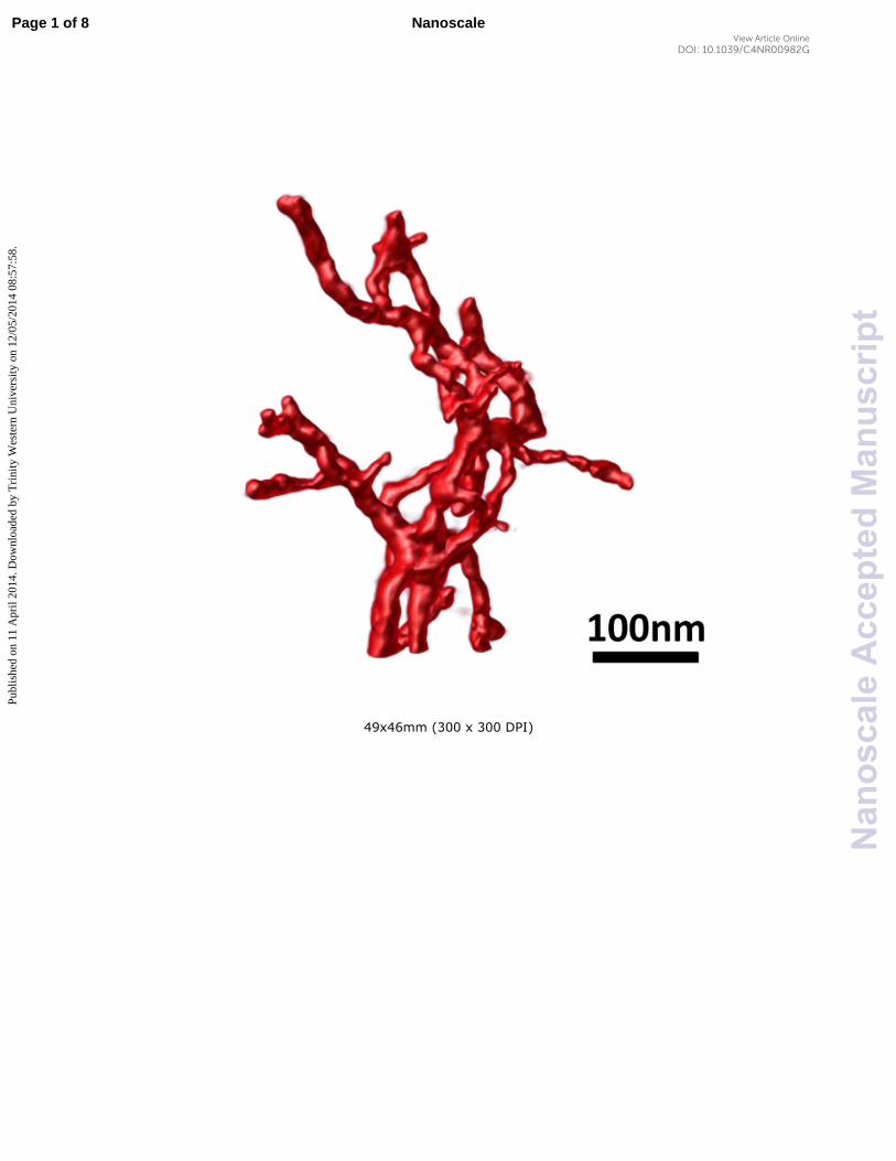
49x46mm (300 x 300 DPI)
Page 1 of 8 Nanoscale
Nan
osca
leA
ccep
ted
Man
uscr
ipt
Publ
ishe
d on
11
Apr
il 20
14. D
ownl
oade
d by
Tri
nity
Wes
tern
Uni
vers
ity o
n 12
/05/
2014
08:
57:5
8.
View Article OnlineDOI: 10.1039/C4NR00982G

Porous 3D network of platinum nanowires has been successfully synthesized by atomic layer
deposition on carbon nanotubes and following calcination.
Page 2 of 8Nanoscale
Nan
osca
leA
ccep
ted
Man
uscr
ipt
Publ
ishe
d on
11
Apr
il 20
14. D
ownl
oade
d by
Tri
nity
Wes
tern
Uni
vers
ity o
n 12
/05/
2014
08:
57:5
8.
View Article OnlineDOI: 10.1039/C4NR00982G
Journal Name RSCPublishing
ARTICLE
This journal is © The Royal Society of Chemistry 2013 J. Name., 2013, 00, 1-3 | 1
Cite this: DOI: 10.1039/x0xx00000x
Received 00th January 2012,
Accepted 00th January 2012
DOI: 10.1039/x0xx00000x
www.rsc.org/
3D network of Pt nanowires by atomic layer
deposition on carbonaceous template
Shaoren Deng, ‡a
Mert Kurttepeli, ‡b Stella Deheryan,
c Daire J. Cott,
c Philippe M.
Vereecken, c, d
Johan A. Martens, d
Sara Bals, b
Gustaaf van Tendeloo,b and
Christophe Detavernier*a
The formation of a 3D network composed of free standing and interconnected Pt nanowires is
achieved by a two-step method, consisting of conformal deposition of Pt by atomic layer
deposition (ALD) on a forest of carbon nanotubes and subsequent removal of the carbonaceous
template. Detailed characterization of this novel 3D nanostructure was carried out by
transmission electron microscopy (TEM) and electrochemical impedance spectroscopy (EIS).
These characterizations showed that this pure 3D nanostructure of platinum is self-supported
and offers an enhancement of the electrochemically active surface area by a factor of 50.
Introduction
As an effective catalyst, platinum (Pt) has been widely used
in many applications including water splitting, fuel cells and
automobile emission control.1-3 Different synthesis methods
have been so far employed to synthesize Pt nanostructures with
various morphologies. Electrospinning was for instance
successfully carried out for the synthesis of Pt nanowires.4
Yang et al. reported the production of Pt nanoparticles by
reducing chloroplatinic acid (H2PtCl6) in formic acid at low
temperature.5 In case of porous Pt structures synthesis, the use
of a template material with a large surface area is widely
preferred. Sun et al. used an aqueous method to grow ultra-
small Pt nanowires on nitrogen-doped carbon nanotubes.6
Sattayasamitsathit et al. demonstrated a delicate three-
dimensional (3D) porous carbon structure decorated with Pt
nanoparticles by electro-depositing.7 3D ordered networks of
platinum nanowires were synthesized by S. Akbar et al. using
lipid as an electrochemical template with a high surface area.
Dealloying Pt-M (Al, Fe, Au…) alloy is another popular way to
fabricate porous Pt nanowires and has therefore been under
intensive research in the recent years.8-10
Atomic layer deposition (ALD) is an effective method to
functionalize porous materials and tune the pore size.11-12
Different types of porous materials, e.g. Pt nanotubes or hybrid
catalysts, have been successfully produced using ALD.13-15 Liu
et al. for instance deposited Pt nanoparticles on carbon
nanotubes (CNTs) support for fuel cell applications.16 On the
other hand, support-free and porous Pt nanostructures can be
advantageous for certain applications, e.g., in aggressive
environments where the supports are potentially not stable. As
an example, Pt nanoparticles dispersed on a carbon support may
suffer from instability issues during oxygen reduction
reactions.17-18
Here, we report ALD of Pt on ordered multi-walled carbon
nanotubes (MWCNTs) and the formation of a 3D network
comprising pure self-supporting Pt nanowires upon removal of
the MWCNTs through annealing. Electrochemical impedance
spectroscopy (EIS) tests showed that the resulting 3D network
of Pt nanowires exhibit a large and electrochemically active
surface area. Henceforth, the ALD Pt coated MWCNTs and the
3D network of Pt nanowires (i.e. after removal of the
carbonaceous support) will be referred to as “Pt-MWCNTs”
and “3D-Pt” throughout this paper, respectively.
Experimental
MWCNTs with 10µm height were synthesized using a
C2H4/H2 mixture gas in a microwave (2.45 GHz) plasma
enhanced chemical vapor deposition chamber (PECVD, TEL,
Japan) on 1nm Co/70nm TiN coated Si wafers. A home built
ALD reactor with base pressure of ~5*10-7 mbar was used for
ALD depositions.19 ALD of Pt was carried out at 200oC with
alternating pulses of (methylcyclopentadienyl)
trimethylplatinum (MeCpPtMe3) (Sigma Aldrich) and ozone
with a concentration of 150 µg per mL supplied by an ozone
generator (Yanco Industry LTD).20 For each pulse, the pulse
pressure was ~0.8 mbar. A Bruker D8 Discovery system was
used for the X-ray fluorescence (XRF) measurements. Scanning
electron microscopy (SEM) and energy dispersive X-ray
spectroscopy (EDS) measurements were done in FEI Quanta
200F. The in situ X-ray Diffraction (XRD) measurements and
the post deposition annealing were carried out in a home
modified Bruker D8 Discovery system. Transmission electron
microscopy (TEM) samples were prepared by scraping off the
Page 3 of 8 Nanoscale
Nan
osca
leA
ccep
ted
Man
uscr
ipt
Publ
ishe
d on
11
Apr
il 20
14. D
ownl
oade
d by
Tri
nity
Wes
tern
Uni
vers
ity o
n 12
/05/
2014
08:
57:5
8.
View Article OnlineDOI: 10.1039/C4NR00982G
ARTICLE Journal Name
2 | J. Name., 2012, 00, 1-3 This journal is © The Royal Society of Chemistry 2012
Pt-containing layer from the substrate surface, and suspending
the resulting powder in ethanol. A drop of this suspension was
deposited on a carbon coated TEM grid. Bright-field TEM
(BFTEM) images and selected area electron diffraction (SAED)
patterns were acquired using a FEI Tecnai F20 TEM operated
at 200 kV. High-angle annular dark field scanning TEM
(HAADF-STEM) images and energy-dispersive X-ray (EDX)
elemental maps were collected using a FEI Titan 60-300 TEM
operated at 300 kV, equipped with the ChemiSTEM system for
EDX analysis. HAADF-STEM electron tomography tilt series
were collected using either a FEI Titan 60-300 TEM operated at
300 kV, or using a FEI Tecnai F20 TEM operated at 200 kV,
both of which equipped with an advanced tomography holder
from Fischione Instruments and the FEI XPlore3D software
package. For the tomography experiments, 71 HAADF-STEM
images were acquired over the range of ±70° with 2° tilt
increments. Alignment and reconstruction of the tomography
data were carried out using the FEI Inspect3D software
package. The reconstructions were performed using the
“Simultaneous Iterative Reconstruction Technique” (SIRT)
with 25 iterations implemented in Inspect 3D. Amira software
(Visage Imaging GmbH) was used for visualizations.
Electrochemical characterization of the samples was done with
1M Na2SO4 in H2O under ambient conditions and a room
temperature. All the chemicals were delivered from Sigma-
Aldrich, USA. The experiments were performed in a three-
electrode electrochemical cell, with a Pt mesh (Sigma-Aldrich,
US) as counter electrode and a Ag/AgCl, KCl (sat'd) (BASi
USA) as reference electrode. Top contacts were made using a
copper tape (Sigma-Aldrich, U.S.A) on four corners of the
working electrode. The active surface area in both set-ups was
equal to 0.95 cm2. Measurements were done using an Autolab
PGSTAT302N potentiostat integrated with frequency response
analyzer and controlled by Nova 1.8 software (Ecochemie,
Netherlands). All electrochemical impedance Spectroscopy
Measurements were performed after Cyclic Voltametry
measurements on the same sample. CV measurements with four
consecutive scans with a sweep rate of 20mV/s from negative
voltages towards positive were carried out. EIS measurements
were performed over a frequency range of 10 KHz to 1 Hz with
an AC amplitude of 10 mV without agiation. Nova V1.8
software was used to do nonlinear least-squares fitting of the
EIS spectra.
Results and discussion
Conformal coating of MWCNTs requires adequate pulse
times of precursor and oxidant during the ALD process. In situ
and ex situ X-ray fluorescence (XRF) characterization has been
proved to be an effective method for identifying the saturation
condition for ALD coating of porous materials.21 50 cycles of
ALD were applied on MWCNTs with different pulse times of
20, 30, 40 and 60 sec of MeCpPtMe3 and ozone with a fixed
pumping time of 60 sec for each half cycle. Ex situ XRF
measurement on this batch of samples showed different
intensities. For pulse times of 40 sec and longer, the intensity of
the PtL fluorescence leveled, which indicates that 40 sec
exposure is sufficient for the conformal coating on the
MWCNTs (Fig. S1). A scanning electron microscopy (SEM)
image of the Pt-MWCNTs (Fig. 1(a)) shows that after 50 cycles
Pt coating, no obvious morphological changes were observed at
the micrometer-scale after ALD. A TEM study of the samples
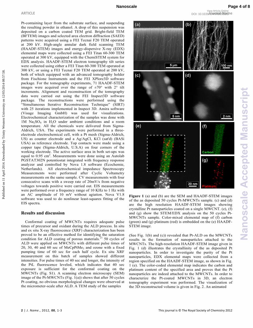
Figure 1 (a) and (b) are the SEM and HAADF-STEM images
of the as deposited 50 cycles Pt-MWCNTs sample. (c) and (d)
are the high resolution HAADF-STEM images showing
crystalline Pt nanoparticles coated on a single MWCNT. (e), (f)
and (g) show the STEM/EDX analysis on the 50 cycles Pt-
MWCNTs sample. Color-mixed elemental map of (f) carbon
(green) and (g) platinum (red) is embedded on the (e) HAADF-
STEM image.
(See Fig. 1(b) and (c)) revealed that Pt-ALD on the MWCNTs
results in the formation of nanoparticles attached to the
MWCNTs. The high-resolution HAADF-STEM image given in
Fig. 1 (d) illustrates the crystallinity of the as deposited Pt
nanoparticles. In order to investigate the purity of the Pt
nanoparticles, EDX elemental maps were collected from a
region specified on the HAADF-STEM image, as shown in Fig.
1 (e). The color-coded elemental map indicates the carbon and
platinum content of the specified area and proves that the Pt
nanoparticles are indeed attached to the MWCNTs. In order to
characterize the Pt-coated MWCNTs in 3D, an electron
tomography experiment was performed. The visualization of
the 3D reconstructed volume is given in Fig. 2. An animated
Page 4 of 8Nanoscale
Nan
osca
leA
ccep
ted
Man
uscr
ipt
Publ
ishe
d on
11
Apr
il 20
14. D
ownl
oade
d by
Tri
nity
Wes
tern
Uni
vers
ity o
n 12
/05/
2014
08:
57:5
8.
View Article OnlineDOI: 10.1039/C4NR00982G
Journal Name ARTICLE
This journal is © The Royal Society of Chemistry 2012 J. Name., 2012, 00, 1-3 | 3
Figure 2 The visualization of the 3D tomography and the
distribution of Pt nanoparticle size from 50 cycles Pt-MWCNTs
sample (only Pt nanoparticles are shown).
version of the tomogram is provided in the supporting
information as a video (See supporting information). The
formation of randomly distributed Pt nanoparticles on the
MWCNTs is clearly observed in the 3D visualization. The size
distribution of the Pt nanoparticles was obtained from the
electron tomography experiment. It was found that the
nanoparticles have an average particle radius around 3nm, as
shown in Fig. 2.
In view of the wide spacing in between neighboring Pt
nanoparticles on the MWCNTs, one could expect that removal
of the carbonaceous support would induce a complete collapse
of the structure. Surprisingly, the overall forest-type
morphology was preserved after calcination of the Pt-
MWCNTs. In Fig. 3, SEM images and EDS results are used to
schematically illustrate the transformation of Pt-MWCNTs into
a free standing 3D-Pt nanostructure. Even though the
MWCNTs were removed during the calcination, the overall
structure was largely preserved; although a clear shrinkage of
the height can be observed. Detailed characterization of the
resulting 3D-Pt sample was carried out by TEM (see Fig. 4.).
Fig. 4(a) and (b) depict this 3D network comprising Pt
nanowires with different diameter ranging from 10 to 50nm.
Such variation of the diameter is likely to result from the
merging of Pt coating on adjacent MWCNTs into larger
crystalline wires, whereas the Pt coating on isolated MWCNTs
Figure 3 A combined figure of schematic illustration, SEM
images and EDS results shows the morphology and elementary
transformation from MWCNTs (a) to Pt-MWCNTs (b) and to
3D-Pt (c).
Figure 4 (a) and (b) are BF-TEM and HAADF-STEM images
of 50 cycles 3D-Pt sample. (c) is the high resolution HAADF-
STEM images of 50 cycles 3D-Pt sample. (d) shows the SAED
pattern of the part of 50 cycles 3D-Pt sample given in (a).
forms thinner nanowires. The high-resolution HAADF-STEM
image shown in Fig. 4 (c) reveals that these Pt nanowires are
zigzag shaped and composed of crystalline nanoparticles. The
SAED pattern (see Fig. 4 (d)) shows no diffraction rings from
Page 5 of 8 Nanoscale
Nan
osca
leA
ccep
ted
Man
uscr
ipt
Publ
ishe
d on
11
Apr
il 20
14. D
ownl
oade
d by
Tri
nity
Wes
tern
Uni
vers
ity o
n 12
/05/
2014
08:
57:5
8.
View Article OnlineDOI: 10.1039/C4NR00982G
ARTICLE Journal Name
4 | J. Name., 2012, 00, 1-3 This journal is © The Royal Society of Chemistry 2012
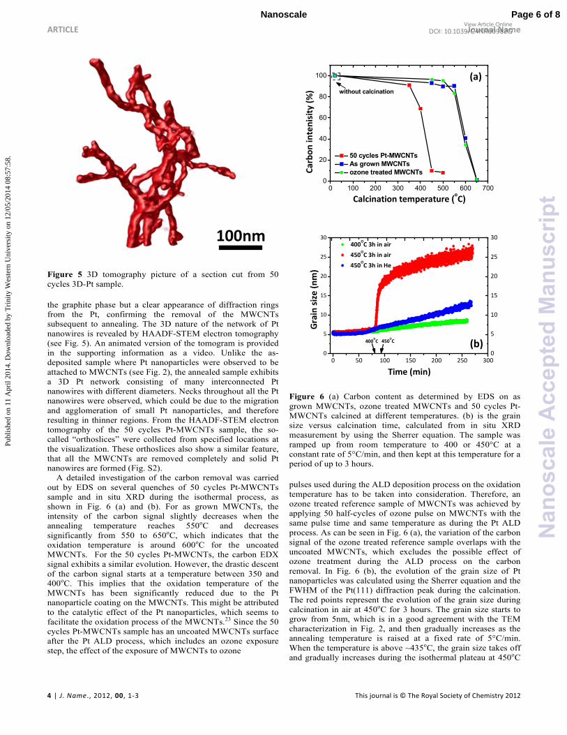
Figure 5 3D tomography picture of a section cut from 50
cycles 3D-Pt sample.
the graphite phase but a clear appearance of diffraction rings
from the Pt, confirming the removal of the MWCNTs
subsequent to annealing. The 3D nature of the network of Pt
nanowires is revealed by HAADF-STEM electron tomography
(see Fig. 5). An animated version of the tomogram is provided
in the supporting information as a video. Unlike the as-
deposited sample where Pt nanoparticles were observed to be
attached to MWCNTs (see Fig. 2), the annealed sample exhibits
a 3D Pt network consisting of many interconnected Pt
nanowires with different diameters. Necks throughout all the Pt
nanowires were observed, which could be due to the migration
and agglomeration of small Pt nanoparticles, and therefore
resulting in thinner regions. From the HAADF-STEM electron
tomography of the 50 cycles Pt-MWCNTs sample, the so-
called “orthoslices” were collected from specified locations at
the visualization. These orthoslices also show a similar feature,
that all the MWCNTs are removed completely and solid Pt
nanowires are formed (Fig. S2).
A detailed investigation of the carbon removal was carried
out by EDS on several quenches of 50 cycles Pt-MWCNTs
sample and in situ XRD during the isothermal process, as
shown in Fig. 6 (a) and (b). For as grown MWCNTs, the
intensity of the carbon signal slightly decreases when the
annealing temperature reaches 550oC and decreases
significantly from 550 to 650oC, which indicates that the
oxidation temperature is around 600oC for the uncoated
MWCNTs. For the 50 cycles Pt-MWCNTs, the carbon EDX
signal exhibits a similar evolution. However, the drastic descent
of the carbon signal starts at a temperature between 350 and
400oC. This implies that the oxidation temperature of the
MWCNTs has been significantly reduced due to the Pt
nanoparticle coating on the MWCNTs. This might be attributed
to the catalytic effect of the Pt nanoparticles, which seems to
facilitate the oxidation process of the MWCNTs.23 Since the 50
cycles Pt-MWCNTs sample has an uncoated MWCNTs surface
after the Pt ALD process, which includes an ozone exposure
step, the effect of the exposure of MWCNTs to ozone
0 100 200 300 400 500 600 700
0
20
40
60
80
100
50 cycles Pt-MWCNTs
As grown MWCNTs
ozone treated MWCNTs
C
arb
on
in
ten
isit
y (
%) without calcination
Calcination temperature (oC)
(a)
0 50 100 150 200 250 3000
5
10
15
20
25
30
400OC 3h in air
450OC 3h in air
450OC 3h in He
Gra
in s
ize
(n
m)
Time (min)
0
5
10
15
20
25
30
400OC 450
OC (b)
Figure 6 (a) Carbon content as determined by EDS on as
grown MWCNTs, ozone treated MWCNTs and 50 cycles Pt-
MWCNTs calcined at different temperatures. (b) is the grain
size versus calcination time, calculated from in situ XRD
measurement by using the Sherrer equation. The sample was
ramped up from room temperature to 400 or 450°C at a
constant rate of 5°C/min, and then kept at this temperature for a
period of up to 3 hours.
pulses used during the ALD deposition process on the oxidation
temperature has to be taken into consideration. Therefore, an
ozone treated reference sample of MWCNTs was achieved by
applying 50 half-cycles of ozone pulse on MWCNTs with the
same pulse time and same temperature as during the Pt ALD
process. As can be seen in Fig. 6 (a), the variation of the carbon
signal of the ozone treated reference sample overlaps with the
uncoated MWCNTs, which excludes the possible effect of
ozone treatment during the ALD process on the carbon
removal. In Fig. 6 (b), the evolution of the grain size of Pt
nanoparticles was calculated using the Sherrer equation and the
FWHM of the Pt(111) diffraction peak during the calcination.
The red points represent the evolution of the grain size during
calcination in air at 450oC for 3 hours. The grain size starts to
grow from 5nm, which is in a good agreement with the TEM
characterization in Fig. 2, and then gradually increases as the
annealing temperature is raised at a fixed rate of 5°C/min.
When the temperature is above ~435oC, the grain size takes off
and gradually increases during the isothermal plateau at 450oC
Page 6 of 8Nanoscale
Nan
osca
leA
ccep
ted
Man
uscr
ipt
Publ
ishe
d on
11
Apr
il 20
14. D
ownl
oade
d by
Tri
nity
Wes
tern
Uni
vers
ity o
n 12
/05/
2014
08:
57:5
8.
View Article OnlineDOI: 10.1039/C4NR00982G
Journal Name ARTICLE
This journal is © The Royal Society of Chemistry 2012 J. Name., 2012, 00, 1-3 | 5
and reaches a range of 24-27 nm at the end of the plateau.
According to the EDX results in Fig. 6 (a), the carbon intensity
drops steeply between 400 and 450oC. Since this coincides with
the dramatic increase of the Pt grain size, the removal of the
carbon appears to assist the merging of the Pt nanoparticles into
larger grains. The limited increase of Pt grain size (blue points)
of a control sample calcined at 450oC in He for 3 hours is in
agreement with this interpretation. The grain size does not
increase spectacularly when then sample was annealed at 400 oC in air for 3 hours (green points), although this long anneal
also resulted in complete removal of the carbon according to
EDX. This indicates that the calcination temperature is an
important factor in the growth of the Pt grains.
Figure 7 SEM pictures of 50 cycles (a), 100 cycles (b,) and 200
cycles (c) Pt-WCNTs samples after calcination at 450oC in air
for 3 hours.
To investigate the effect of the amount of Pt on the
morphology after carbon removal, 100 and 200 cycles Pt-
MWCNTs samples were also annealed using the same process.
SEM images of the annealed samples are shown in Fig. 7(a) –
(c). For all the samples, a similar morphology was observed for
the 3D-Pt structure. However, a considerable decrease of the
overall layer thickness was observed. The thicknesses of 50,
100 and 200 cycles 3D-Pt were measured as ~5.82, ~6.82 and
~7.0µm, respectively. The reduced shrinkage of the height for
the sample with more ALD Pt cycles indicates that the presence
of a larger amount of as deposited Pt coating reduces the
shrinkage during calcination.
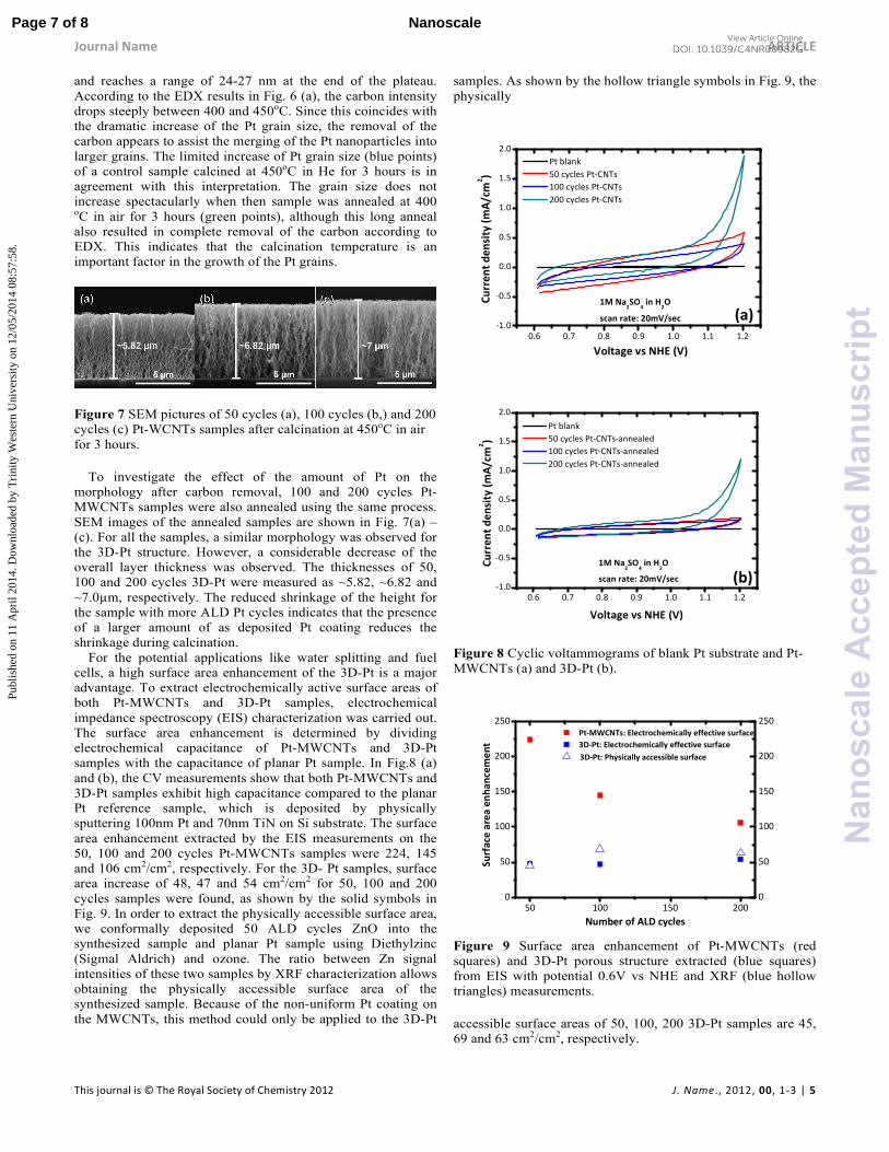
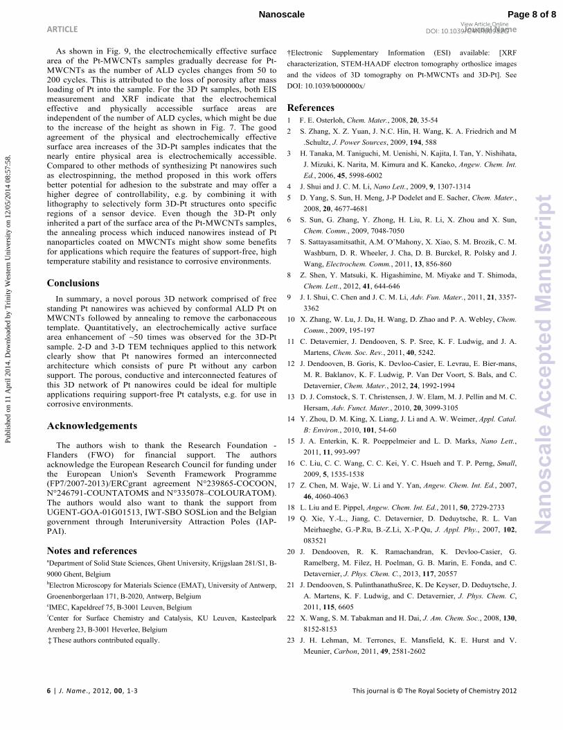
For the potential applications like water splitting and fuel
cells, a high surface area enhancement of the 3D-Pt is a major
advantage. To extract electrochemically active surface areas of
both Pt-MWCNTs and 3D-Pt samples, electrochemical
impedance spectroscopy (EIS) characterization was carried out.
The surface area enhancement is determined by dividing
electrochemical capacitance of Pt-MWCNTs and 3D-Pt
samples with the capacitance of planar Pt sample. In Fig.8 (a)
and (b), the CV measurements show that both Pt-MWCNTs and
3D-Pt samples exhibit high capacitance compared to the planar
Pt reference sample, which is deposited by physically
sputtering 100nm Pt and 70nm TiN on Si substrate. The surface
area enhancement extracted by the EIS measurements on the
50, 100 and 200 cycles Pt-MWCNTs samples were 224, 145
and 106 cm2/cm2, respectively. For the 3D- Pt samples, surface
area increase of 48, 47 and 54 cm2/cm2 for 50, 100 and 200
cycles samples were found, as shown by the solid symbols in
Fig. 9. In order to extract the physically accessible surface area,
we conformally deposited 50 ALD cycles ZnO into the
synthesized sample and planar Pt sample using Diethylzinc
(Sigmal Aldrich) and ozone. The ratio between Zn signal
intensities of these two samples by XRF characterization allows
obtaining the physically accessible surface area of the
synthesized sample. Because of the non-uniform Pt coating on
the MWCNTs, this method could only be applied to the 3D-Pt
samples. As shown by the hollow triangle symbols in Fig. 9, the
physically
0.6 0.7 0.8 0.9 1.0 1.1 1.2
-1.0
-0.5
0.0
0.5
1.0
1.5
2.0
1M Na2SO
4 in H
2O
scan rate: 20mV/sec
C
urr
en
t d
en
sity
(m
A/c
m2)
Pt blank
50 cycles Pt-CNTs
100 cycles Pt-CNTs
200 cycles Pt-CNTs
Voltage vs NHE (V)
(a)
0.6 0.7 0.8 0.9 1.0 1.1 1.2
-1.0
-0.5
0.0
0.5
1.0
1.5
2.0
Cu
rre
nt
de
nsi
ty (
mA
/cm
2)
Voltage vs NHE (V)
Pt blank
50 cycles Pt-CNTs-annealed
100 cycles Pt-CNTs-annealed
200 cycles Pt-CNTs-annealed
1M Na2SO
4 in H
2O
scan rate: 20mV/sec
(b)
Figure 8 Cyclic voltammograms of blank Pt substrate and Pt-
MWCNTs (a) and 3D-Pt (b).
50 100 150 2000
50
100
150
200
250
Pt-MWCNTs: Electrochemically effective surface
3D-Pt: Electrochemically effective surface
Su
rfa
ce a
rea
en
ha
nce
me
nt
Number of ALD cycles
0
50
100
150
200
250
3D-Pt: Physically accessible surface
Figure 9 Surface area enhancement of Pt-MWCNTs (red
squares) and 3D-Pt porous structure extracted (blue squares)
from EIS with potential 0.6V vs NHE and XRF (blue hollow
triangles) measurements.
accessible surface areas of 50, 100, 200 3D-Pt samples are 45,
69 and 63 cm2/cm2, respectively.
Page 7 of 8 Nanoscale
Nan
osca
leA
ccep
ted
Man
uscr
ipt
Publ
ishe
d on
11
Apr
il 20
14. D
ownl
oade
d by
Tri
nity
Wes
tern
Uni
vers
ity o
n 12
/05/
2014
08:
57:5
8.
View Article OnlineDOI: 10.1039/C4NR00982G
ARTICLE Journal Name
6 | J. Name., 2012, 00, 1-3 This journal is © The Royal Society of Chemistry 2012
As shown in Fig. 9, the electrochemically effective surface
area of the Pt-MWCNTs samples gradually decrease for Pt-
MWCNTs as the number of ALD cycles changes from 50 to
200 cycles. This is attributed to the loss of porosity after mass
loading of Pt into the sample. For the 3D Pt samples, both EIS
measurement and XRF indicate that the electrochemical
effective and physically accessible surface areas are
independent of the number of ALD cycles, which might be due
to the increase of the height as shown in Fig. 7. The good
agreement of the physical and electrochemically effective
surface area increases of the 3D-Pt samples indicates that the
nearly entire physical area is electrochemically accessible.
Compared to other methods of synthesizing Pt nanowires such
as electrospinning, the method proposed in this work offers
better potential for adhesion to the substrate and may offer a
higher degree of controllability, e.g. by combining it with
lithography to selectively form 3D-Pt structures onto specific
regions of a sensor device. Even though the 3D-Pt only
inherited a part of the surface area of the Pt-MWCNTs samples,
the annealing process which induced nanowires instead of Pt
nanoparticles coated on MWCNTs might show some benefits
for applications which require the features of support-free, high
temperature stability and resistance to corrosive environments.
Conclusions
In summary, a novel porous 3D network comprised of free
standing Pt nanowires was achieved by conformal ALD Pt on
MWCNTs followed by annealing to remove the carbonaceous
template. Quantitatively, an electrochemically active surface
area enhancement of ~50 times was observed for the 3D-Pt
sample. 2-D and 3-D TEM techniques applied to this network
clearly show that Pt nanowires formed an interconnected
architecture which consists of pure Pt without any carbon
support. The porous, conductive and interconnected features of
this 3D network of Pt nanowires could be ideal for multiple
applications requiring support-free Pt catalysts, e.g. for use in
corrosive environments.
Acknowledgements
The authors wish to thank the Research Foundation -
Flanders (FWO) for financial support. The authors
acknowledge the European Research Council for funding under
the European Union's Seventh Framework Programme
(FP7/2007-2013)/ERCgrant agreement N°239865-COCOON,
N°246791-COUNTATOMS and N°335078–COLOURATOM).
The authors would also want to thank the support from
UGENT-GOA-01G01513, IWT-SBO SOSLion and the Belgian
government through Interuniversity Attraction Poles (IAP-
PAI).
Notes and references aDepartment of Solid State Sciences, Ghent University, Krijgslaan 281/S1, B-
9000 Ghent, Belgium bElectron Microscopy for Materials Science (EMAT), University of Antwerp,
Groenenborgerlaan 171, B-2020, Antwerp, Belgium cIMEC, Kapeldreef 75, B-3001 Leuven, Belgium dCenter for Surface Chemistry and Catalysis, KU Leuven, Kasteelpark
Arenberg 23, B-3001 Heverlee, Belgium
‡ These authors contributed equally.
†Electronic Supplementary Information (ESI) available: [XRF
characterization, STEM-HAADF electron tomography orthoslice images
and the videos of 3D tomography on Pt-MWCNTs and 3D-Pt]. See
DOI: 10.1039/b000000x/
References
1 F. E. Osterloh, Chem. Mater., 2008, 20, 35-54 2 S. Zhang, X. Z. Yuan, J. N.C. Hin, H. Wang, K. A. Friedrich and M
.Schultz, J. Power Sources, 2009, 194, 588
3 H. Tanaka, M. Taniguchi, M. Uenishi, N. Kajita, I. Tan, Y. Nishihata,
J. Mizuki, K. Narita, M. Kimura and K. Kaneko, Angew. Chem. Int.
Ed., 2006, 45, 5998-6002
4 J. Shui and J. C. M. Li, Nano Lett., 2009, 9, 1307-1314
5 D. Yang, S. Sun, H. Meng, J-P Dodelet and E. Sacher, Chem. Mater.,
2008, 20, 4677-4681
6 S. Sun, G. Zhang, Y. Zhong, H. Liu, R. Li, X. Zhou and X. Sun,
Chem. Comm., 2009, 7048-7050
7 S. Sattayasamitsathit, A.M. O’Mahony, X. Xiao, S. M. Brozik, C. M.
Washburn, D. R. Wheeler, J. Cha, D. B. Burckel, R. Polsky and J.
Wang, Electrochem. Comm., 2011, 13, 856-860
8 Z. Shen, Y. Matsuki, K. Higashimine, M. Miyake and T. Shimoda,
Chem. Lett., 2012, 41, 644-646
9 J. I. Shui, C. Chen and J. C. M. Li, Adv. Fun. Mater., 2011, 21, 3357-
3362
10 X. Zhang, W. Lu, J. Da, H. Wang, D. Zhao and P. A. Webley, Chem.
Comm., 2009, 195-197
11 C. Detavernier, J. Dendooven, S. P. Sree, K. F. Ludwig, and J. A.
Martens, Chem. Soc. Rev., 2011, 40, 5242.
12 J. Dendooven, B. Goris, K. Devloo-Casier, E. Levrau, E. Bier-mans,
M. R. Baklanov, K. F. Ludwig, P. Van Der Voort, S. Bals, and C.
Detavernier, Chem. Mater., 2012, 24, 1992-1994
13 D. J. Comstock, S. T. Christensen, J. W. Elam, M. J. Pellin and M. C.
Hersam, Adv. Funct. Mater., 2010, 20, 3099-3105
14 Y. Zhou, D. M. King, X. Liang, J. Li and A. W. Weimer, Appl. Catal.
B: Environ., 2010, 101, 54-60
15 J. A. Enterkin, K. R. Poeppelmeier and L. D. Marks, Nano Lett.,
2011, 11, 993-997
16 C. Liu, C. C. Wang, C. C. Kei, Y. C. Hsueh and T. P. Perng, Small,
2009, 5, 1535-1538
17 Z. Chen, M. Waje, W. Li and Y. Yan, Angew. Chem. Int. Ed., 2007,
46, 4060-4063
18 L. Liu and E. Pippel, Angew. Chem. Int. Ed., 2011, 50, 2729-2733
19 Q. Xie, Y.-L., Jiang, C. Detavernier, D. Deduytsche, R. L. Van
Meirhaeghe, G.-P.Ru, B.-Z.Li, X.-P.Qu, J. Appl. Phy., 2007, 102,
083521
20 J. Dendooven, R. K. Ramachandran, K. Devloo-Casier, G.
Ramelberg, M. Filez, H. Poelman, G. B. Marin, E. Fonda, and C.
Detavernier, J. Phys. Chem. C., 2013, 117, 20557
21 J. Dendooven, S. PulinthanathuSree, K. De Keyser, D. Deduytsche, J.
A. Martens, K. F. Ludwig, and C. Detavernier, J. Phys. Chem. C,
2011, 115, 6605
22 X. Wang, S. M. Tabakman and H. Dai, J. Am. Chem. Soc., 2008, 130,
8152-8153
23 J. H. Lehman, M. Terrones, E. Mansfield, K. E. Hurst and V.
Meunier, Carbon, 2011, 49, 2581-2602
Page 8 of 8Nanoscale
Nan
osca
leA
ccep
ted
Man
uscr
ipt
Publ
ishe
d on
11
Apr
il 20
14. D
ownl
oade
d by
Tri
nity
Wes
tern
Uni
vers
ity o
n 12
/05/
2014
08:
57:5
8.
View Article OnlineDOI: 10.1039/C4NR00982G