Embed Size (px)
Citation preview

ViaLiteHD Development programming kit
User Guide
HRx-HD-DEV103-HB-6
CR3487 21/07/2016
Pulse Power & Measurement Ltd, 65 Shrivenham Hundred Business Park, Watchfield, Swindon, Wiltshire SN68TY, UK
Tel +44 (0)1793 784389 Fax +44 (0)1793 784391 Email [email protected] Web www.vialite.com
HRX-HD-DEV103-HB-6 VIALITEHD DEVELOPMENT BOARD HANDBOOK
2
Instrument Care and Safety Information
Please read the whole of this section before using your ViaLiteHD product. It contains important safety
information and will enable you to get the most out of your Fibre Optic Link. Electrical Safety
The ViaLiteHD development kit power supply is a class 2 product (double isolated). When operating the equipment note the following precautions:
Hazardous voltages exist within the equipment. There are no user serviceable parts inside; the covers should only be removed by a qualified technician.
There are no user replaceable fuses. The ViaLiteHD development board is a safety extra-low voltage (SELV) device. ESD Precautions
The ViaLiteHD systems are equipped with high frequency active electronics, without the correct handing they will be susceptible to damage. Precautions for handling electro-static sensitive devices should be observed when handling all ViaLiteHD modules. Technicians should ensure that they use effective personal grounding (i.e. ESD wrist strap etc.) when servicing the equipment. Any equipment or tools used should be grounded to prevent static charge build-up. Good practice should be observed at all times for reference see relevant standards. EN 61340-5-1, “Protection of Electronic Devices from Electrostatic Phenomena – General Requirements”
Optical Safety
The ViaLiteHD RF Fibre Optic Transmitters, Dual Transmitters and Transceivers contain optical sources (usually laser diodes) operating at nominal wavelengths of 1270nm to 1610nm. These devices are rated as EN60825-1:2007 as CLASS 1 radiation emitting devices. A class 1 laser is safe under all conditions of normal use. When operating the equipment note the following precautions:
Never look into the end of an optical fibre directly or by reflection either with the naked eye or through an optical instrument.
Never leave equipment with radiating bare fibres – always cap the connectors.
Do not remove equipment external covers when operating.

HRX-HD-DEV103-HB-6 VIALITEHD DEVELOPMENT BOARD HANDBOOK
3
Table of contents
1 INTRODUCTION ................................................................................................................................................................................. 5 Development kit, inventory 5 1.1 Internal architecture, block diagram 6 1.2
2 SOFTWARE INSTALLATION .............................................................................................................................................................. 7 Computer requirement 7 2.1 Software installation procedure 7 2.2
3 DEVELOPMENT BOARD PHYSICAL ............................................................................................................................................... 10 Setting up the hardware interfaces 10 3.1 ViaLiteHD and ViaLite Classic compatibility 10 3.2 Main board, external connections 10 3.3 Main board, USB connection 11 3.4 Main board, power 15 way D type 11 3.5 Power supply module connections 11 3.6 Main board, signal 9 way D type 11 3.7 Physical interfaces, module interface board 12 3.8
3.8.1 Physical interfaces, module interface board, connection to the main board 12 3.8.2 Physical interfaces, module interface board, connection to a plug in module 13 3.8.3 Physical interfaces, module interface board, connection to an OEM module 13 3.8.4 Physical interfaces, module interface board, connection to an EDGE module 14
Physical interface, test signals 14 3.93.9.1 Physical interface, test signals, to modules 14 3.9.2 Physical interface, test signals, common 15 3.9.3 Physical interface, test hooks 15 3.9.4 Physical interface, alarm simulation connectors 15
Activity LEDs 16 3.10 More information on connected hardware 16 3.11
4 SOFTWARE ...................................................................................................................................................................................... 17 Starting the program 17 4.1 Start-up screen 17 4.2
4.2.1 Start-up screen, general information 17 4.2.2 Start-up screen, module information window 17 4.2.3 Start-up screen, accessing module control screen 17
Control screen, general 18 4.34.3.1 Control screen, general, information panel 18 4.3.2 Control screen, general, panel LED colours 18 4.3.3 Control screen, general, configuration control buttons 18 4.3.4 Control screen, general, gain adjustment 18
Control screen, general, gain adjustment, gain control priorities ..................................................... 18 4.3.4.1 Control screen, general, gain adjustment, AGC mode for RX functions........................................... 18 4.3.4.2 Control screen, general, gain adjustment, soft gain control ............................................................. 18 4.3.4.3 Control screen, general, gain adjustment, automatic gain control ................................................... 18 4.3.4.4 Control screen, general, gain adjustment, default gain .................................................................... 19 4.3.4.5
Control screen, general, Part number and serial number window 19 4.4 TX module control screen 20 4.5
4.5.1 TX module control screen, Module A configuration 20 4.5.2 TX module control screen, Module A monitor and alarm 20 4.5.3 TX module control screen, Module A alarms 20 4.5.4 TX module control screen, Module A status 21 4.5.5 TX module control screen, Configuration control, buttons 21 4.5.6 TX module control screen, closing the screen 21
DWDM TX module control screen 22 4.64.6.1 DWDM TX module control screen, Module A configuration 22 4.6.2 DWDM TX module control screen, Module A monitor and alarm 22 4.6.3 DWDM TX module control screen, Module A alarms 22 4.6.4 DWDM TX module control screen, Module A status 23 4.6.5 DWDM TX module control screen, Configuration control, buttons 23 4.6.6 DWDM TX module control screen, closing the screen 23
RX module control screen 24 4.74.7.1 RX module control screen, Module A configuration 24 4.7.2 RX module control screen, Module A monitor and alarm 24 4.7.3 RX module control screen, Module A alarms 24 4.7.4 RX module control screen, Module A status 25 4.7.5 RX module control screen, Configuration control, buttons 25 4.7.6 RX module control screen, closing the screen 25
LNB control screen, accessing 25 4.84.8.1 LNB control screen 26 4.8.2 LNB control screen, alarms 26 4.8.3 LNB control screen, status 26 4.8.4 LNB control screen, Configuration control, buttons 26 4.8.5 LNA control screen, closing the screen 26
TRX control screen 27 4.9 Dual TX control screen 28 4.10 Dual RX control screen 29 4.11
HRX-HD-DEV103-HB-6 VIALITEHD DEVELOPMENT BOARD HANDBOOK
4
Serial Digital control screen, accessing 30 4.124.12.1 Serial Digital module control screen, monitor and alarm 30 4.12.2 Serial Digital module control screen, alarms 30 4.12.3 Serial Digital module control screen, status 30 4.12.4 Serial Digital module control screen, Configuration control, buttons 31 4.12.5 Serial Digital module control screen, closing the screen 31
Switch control screen, accessing 32 4.134.13.1 Switch module control screen, Configuration 32 4.13.2 Switch module control screen, switch priority 32 4.13.3 Switch module control screen, Mode setting 32 4.13.4 Switch module control screen, alarms 32 4.13.5 Switch module control screen, closing the screen 32
Switched splitter, control screen, accessing 33 4.144.14.1 Switched splitter module control screen, Configuration 33 4.14.2 Switched splitter module control screen, switch priority 33 4.14.3 Switched splitter module control screen, Monitor 33 4.14.4 Switched splitter module control screen, alarms 33 4.14.5 Switched splitter module control screen, closing the screen 33
Modules with limited functionality 34 4.15 Unsupported Modules 34 4.16 Closing the program 34 4.17
5 CONTROLLING VIALITEHD MODULE USING I2C .......................................................................................................................... 35 Example of setting module gain 35 5.1 I2C map for the TX function 36 5.2 I2C map for the RX function 37 5.3 I2C map for the on board LNB power supply function 38 5.4 I2C map for the Serial Digital function 39 5.5 I2C map for the Switch function 40 5.6
6 MAINTENANCE AND FAULT-FINDING GUIDE ................................................................................................................................ 41
7 GLOSSARY ...................................................................................................................................................................................... 42
8 PRODUCT WARRANTY ................................................................................................................................................................... 43
9 FCC APPROVAL .............................................................................................................................................................................. 44
HRX-HD-DEV103-HB-6 VIALITEHD DEVELOPMENT BOARD HANDBOOK
5
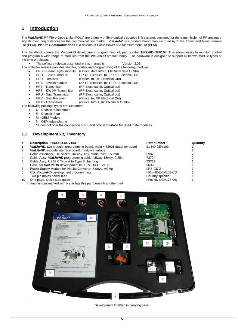
1 Introduction
The ViaLiteHD RF Fibre Optic Links (FOLs) are a family of fibre optically coupled link systems designed for the transmission of RF analogue signals over long distances for the communications market. ViaLiteHD is a product brand manufactured by Pulse Power and Measurement Ltd (PPM). ViaLite Communications is a division of Pulse Power and Measurement Ltd (PPM). This handbook covers the ViaLiteHD development programming kit, part number HRX-HD-DEV103. This allows users to monitor, control and program a wide range of modules from the ViaLiteHD product family. The hardware is designed to support all known module types at the time of release.
The software release described in this manual is: Version 3.01 The software release provides monitor, control and programming of the following modules
HRB – Serial Digital module (Optical data In/out, Electrical data Out/In)
HRD – Splitter module (1 * RF Electrical In, 2 * RF Electrical Out)
HRR - Receiver (Optical In, RF Electrical Out)
HRS – Switch module (2 * RF Electrical In, 1 * RF Electrical Out)
HRT - Transmitter (RF Electrical In, Optical out)
HRT – DWDM Transmitter (RF Electrical In, Optical out)
HRU - Dual Transmitter (RF Electrical In, Optical out)
HRV - Dual Receiver (Optical In, RF Electrical Out)
HRX - Transceiver (Optical In/out, RF Electrical Out/In) The following package types are supported
D - Chassis Blind mate*
R - Chassis Plug
M - OEM Module
N - OEM edge plug-in * Does not offer the connection of RF and optical interface for Blind mate modules.
Development kit, inventory 1.1
# Description HRX-HD-DEV103. Part number Quantity 1 ViaLiteHD, two module, programming board, main + 53901 daughter board 81-HD-DEV103 1 2 ViaLiteHD, module interface board, module interface 2 3 Cable assembly, IDC socket, 34 way, key, strain relief, 150mm 59822 2 4 Cable Assy, ViaLiteHD programming cable, 15way-15way, 0.25m 73724 2 5 Cable Assy, USB2.0 Type A to Type B, 1m long 73727 1 6 Case, for ViaLiteHD development kit, HRx-HD-DEV103 96028 1 7 Power Supply Module for ViaLite Converter Sleeve, AC i/p LPS-CS-2 1 8 CD, ViaLiteHD development programming HRx-HD-DEV103-CD 1 9 Two pin mains power lead Country specific 1 10 One page, Quick start guide HRx-HD-DEV103-QS 1 * any number marked with a star has this part beneath another part
Development kit fitted in carrying case
1
7
5
3 3
2*
4
9
10
2*
4
6
8*
HRX-HD-DEV103-HB-6 VIALITEHD DEVELOPMENT BOARD HANDBOOK
6
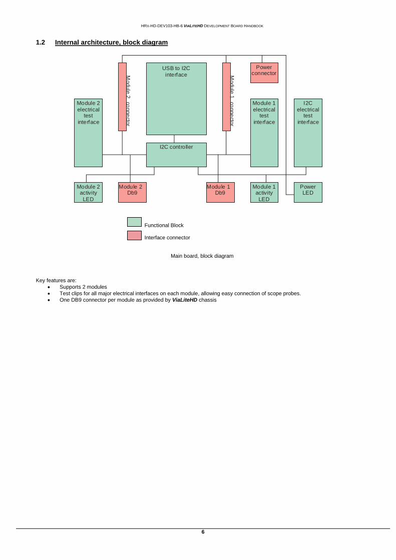
Internal architecture, block diagram 1.2
Functional Block Interface connector
Main board, block diagram Key features are:
Supports 2 modules
Test clips for all major electrical interfaces on each module, allowing easy connection of scope probes.
One DB9 connector per module as provided by ViaLiteHD chassis
Module 2 activity
LED
Module 2Db9
Module 1Db9
Module 1 activity
LED
Power LED
Module 1
electrical test
interface
Power connector
Module 2
electrical test
interface
I2C
electrical test
interface
Module
2 co
nne
ctor
Module
1 co
nne
ctor
USB to I2C
interface
I2C controller
HRX-HD-DEV103-HB-6 VIALITEHD DEVELOPMENT BOARD HANDBOOK
7
2 Software installation
Before the development kit is used the software needs to be installed.
Computer requirement 2.1
It is necessary to ensure that your connected computer is correctly configured. Firstly ensure that your PC meets the minimum requirements, it must have:
1. Windows XP, service pack 2 or later (functionality confirmed on Windows Vista, Windows 7 and 8) 2. Microsoft Internet Explorer 8.0 or later 3. One USB port
Software installation procedure 2.2
To install the software follow these steps. Software should be installed before connecting to the board.
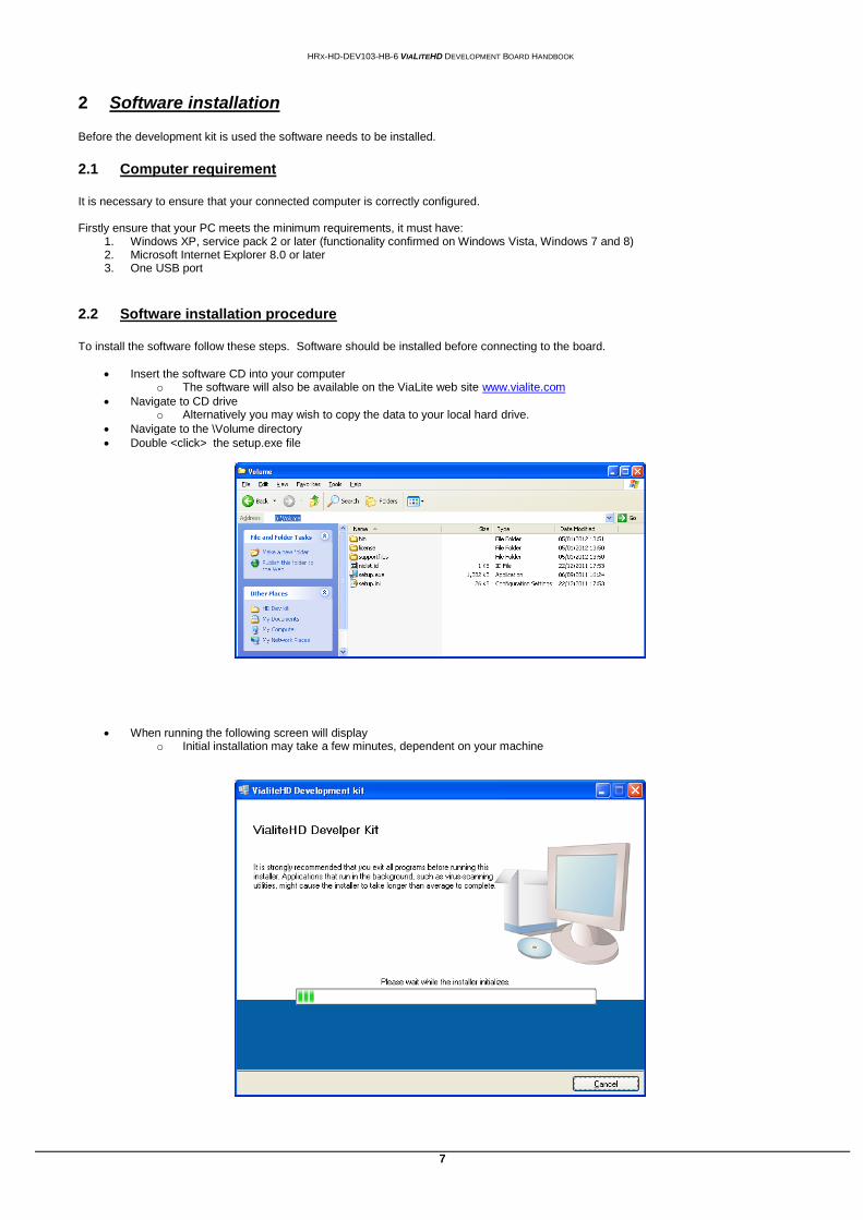
Insert the software CD into your computer o The software will also be available on the ViaLite web site www.vialite.com
Navigate to CD drive o Alternatively you may wish to copy the data to your local hard drive.
Navigate to the \Volume directory
Double <click> the setup.exe file
When running the following screen will display o Initial installation may take a few minutes, dependent on your machine
HRX-HD-DEV103-HB-6 VIALITEHD DEVELOPMENT BOARD HANDBOOK
8
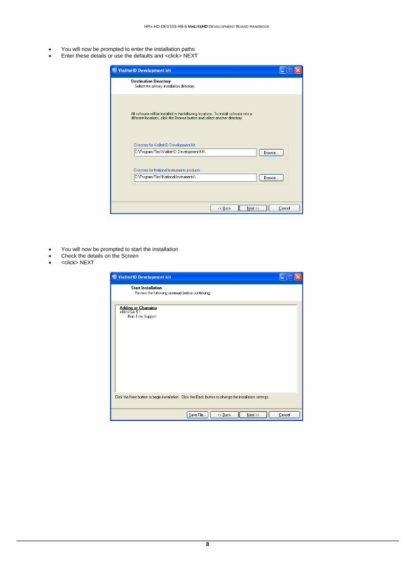
You will now be prompted to enter the installation paths
Enter these details or use the defaults and <click> NEXT
You will now be prompted to start the installation
Check the details on the Screen
<click> NEXT
HRX-HD-DEV103-HB-6 VIALITEHD DEVELOPMENT BOARD HANDBOOK
9
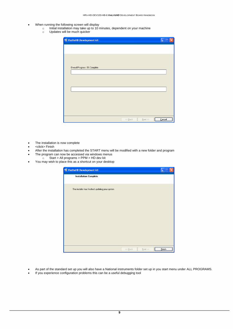
When running the following screen will display o Initial installation may take up to 10 minutes, dependent on your machine o Updates will be much quicker
The installation is now complete
<click> Finish
After the installation has completed the START menu will be modified with a new folder and program
The program can now be accessed via windows menus o Start > All programs > PPM > HD dev kit
You may wish to place this as a shortcut on your desktop
As part of the standard set up you will also have a National instruments folder set up in you start menu under ALL PROGRAMS.
If you experience configuration problems this can be a useful debugging tool

HRX-HD-DEV103-HB-6 VIALITEHD DEVELOPMENT BOARD HANDBOOK
10
3 Development board physical
Setting up the hardware interfaces 3.1
The development kit must be correctly connected for it to operate. The following connections must be made, in this order.
Connect the supplied USB cable type A end to your PC.
Connect the USB cable type B end to Daughter board connector J2. o You should observe the daughter board LED DS1 flashing.
It may take up to 10 second to establish communication o This shows USB communication has been established.
Turn the mains power OFF.
Connect the LPS-CS-2 power supply to the main board, via the 15 way D type J17.
Connect the LPS-CS-2 to its AC power source via the supplied mains cable.
Turn ON the mains power. o The +12V LED should illuminate.
Connect the supplied ribbon cable 59822 to position J6 for module 1 on the motherboard.
Connect the supplied ribbon cable 59822 to position J13 for module 2 on the motherboard. o Note this connector has a keyway which must be aligned.
Connect the other end of the ribbon cable to module interface board J5 (or J12).
Connect the module interface boards to your ViaLiteHD device under test. o ONLY 1 device maybe connected to each module interface board.
WARNING, connection of more than 1 device may cause damage. o Use J1 (or J8) for OEM units. o Use J2 (or J16) for EDGE unit (NOTE the edge connector can only be inserted one way). o Use J4 (or J11) for Plug in units. o The IDs in brackets are for the second module interface board.
ViaLiteHD and ViaLite Classic compatibility 3.2
This development kit will only work with ViaLiteHD equipment; it does not support ViaLite Classic equipment.
Main board, external connections 3.3
USB interface DB15 interface +12V power
Cable to module 1 interconnect board
Cable to module 2 interconnect board
DB9 interface to module 2 DB9 interface to module 1
Daughter board
USB activity LED DS1
+12V power LED
Module 1 I2C activity LED
Module 2 I2C activity LED
HRX-HD-DEV103-HB-6 VIALITEHD DEVELOPMENT BOARD HANDBOOK
11
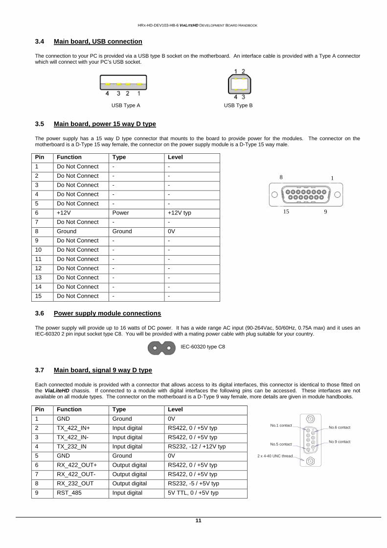
Main board, USB connection 3.4
The connection to your PC is provided via a USB type B socket on the motherboard. An interface cable is provided with a Type A connector which will connect with your PC’s USB socket.
Main board, power 15 way D type 3.5
The power supply has a 15 way D type connector that mounts to the board to provide power for the modules. The connector on the motherboard is a D-Type 15 way female, the connector on the power supply module is a D-Type 15 way male.
Pin Function Type Level
1 Do Not Connect - -
2 Do Not Connect - -
3 Do Not Connect - -
4 Do Not Connect - -
5 Do Not Connect - -
6 +12V Power +12V typ
7 Do Not Connect - -
8 Ground Ground 0V
9 Do Not Connect - -
10 Do Not Connect - -
11 Do Not Connect - -
12 Do Not Connect - -
13 Do Not Connect - -
14 Do Not Connect - -
15 Do Not Connect - -
Power supply module connections 3.6
The power supply will provide up to 16 watts of DC power. It has a wide range AC input (90-264Vac, 50/60Hz, 0.75A max) and it uses an IEC-60320 2 pin input socket type C8. You will be provided with a mating power cable with plug suitable for your country.
Main board, signal 9 way D type 3.7
Each connected module is provided with a connector that allows access to its digital interfaces, this connector is identical to those fitted on the ViaLiteHD chassis. If connected to a module with digital interfaces the following pins can be accessed. These interfaces are not available on all module types. The connector on the motherboard is a D-Type 9 way female, more details are given in module handbooks.
Pin Function Type Level
1 GND Ground 0V
2 TX_422_IN+ Input digital RS422, 0 / +5V typ
3 TX_422_IN- Input digital RS422, 0 / +5V typ
4 TX_232_IN Input digital RS232, -12 / +12V typ
5 GND Ground 0V
6 RX_422_OUT+ Output digital RS422, 0 / +5V typ
7 RX_422_OUT- Output digital RS422, 0 / +5V typ
8 RX_232_OUT Output digital RS232, -5 / +5V typ
9 RST_485 Input digital 5V TTL, 0 / +5V typ
USB Type B USB Type A
IEC-60320 type C8
No.1 contact
2 x 4-40 UNC thread
9
1
6
5
No.5 contact
No.6 contact
No.9 contact
9 15
1
9
8
HRX-HD-DEV103-HB-6 VIALITEHD DEVELOPMENT BOARD HANDBOOK
12
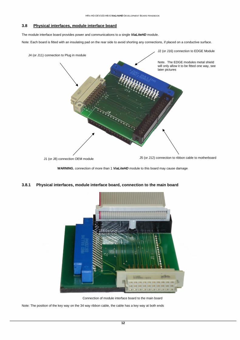
Physical interfaces, module interface board 3.8
The module interface board provides power and communications to a single ViaLiteHD module. Note: Each board is fitted with an insulating pad on the rear side to avoid shorting any connections, if placed on a conductive surface.
WARNING, connection of more than 1 ViaLiteHD module to this board may cause damage
3.8.1 Physical interfaces, module interface board, connection to the main board
Connection of module interface board to the main board
Note: The position of the key way on the 34 way ribbon cable, the cable has a key way at both ends
J2 (or J16) connection to EDGE Module Note. The EDGE modules metal shield will only allow it to be fitted one way, see later pictures
J5 (or J12) connection to ribbon cable to motherboard J1 (or J8) connection OEM module
J4 (or J11) connection to Plug in module
HRX-HD-DEV103-HB-6 VIALITEHD DEVELOPMENT BOARD HANDBOOK
13
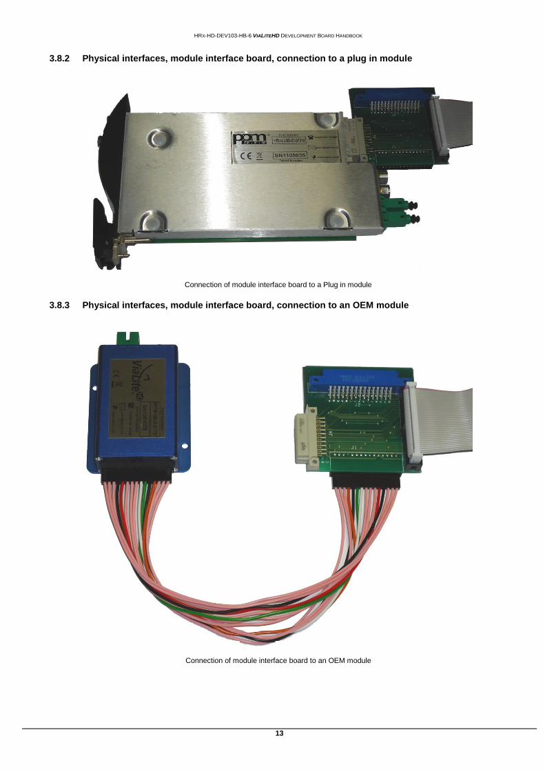
3.8.2 Physical interfaces, module interface board, connection to a plug in module
Connection of module interface board to a Plug in module
3.8.3 Physical interfaces, module interface board, connection to an OEM module
Connection of module interface board to an OEM module
HRX-HD-DEV103-HB-6 VIALITEHD DEVELOPMENT BOARD HANDBOOK
14
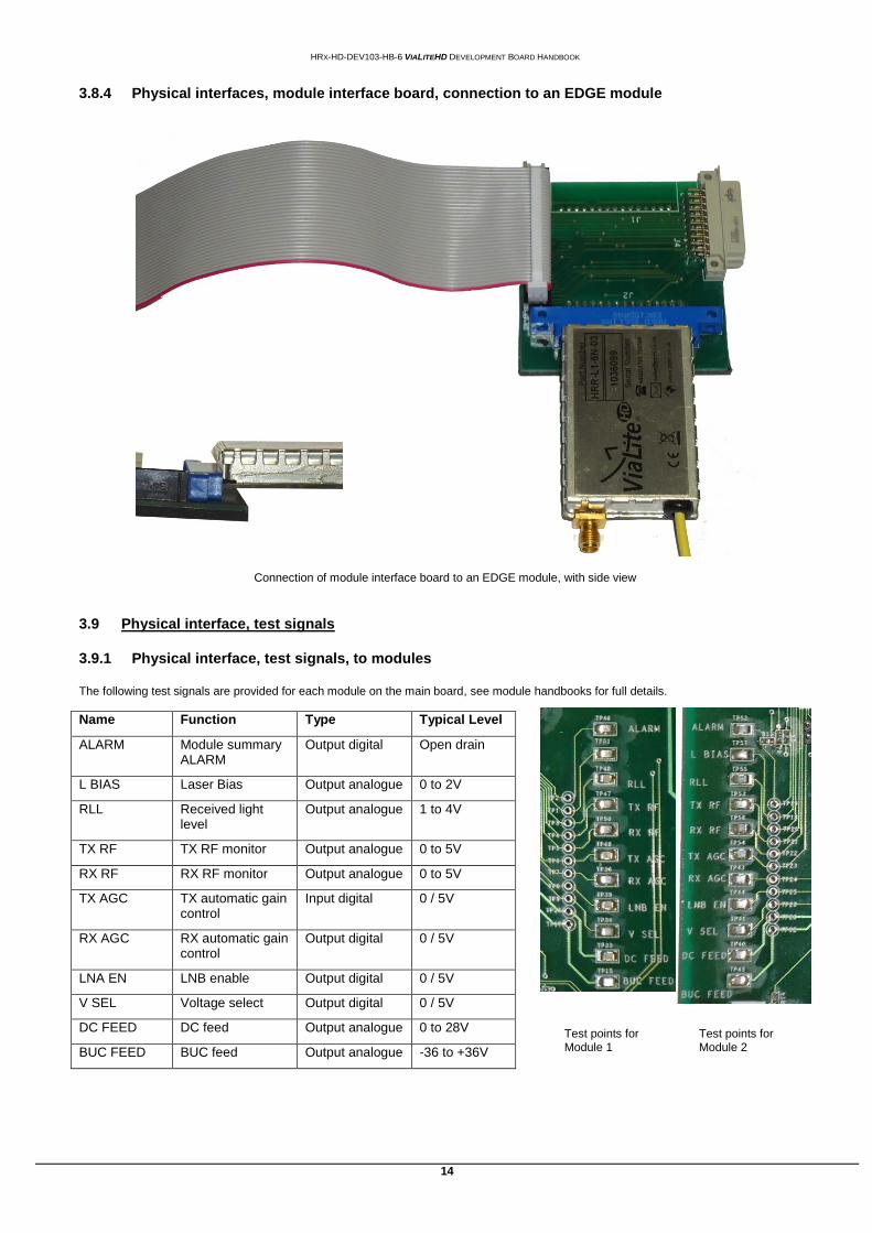
3.8.4 Physical interfaces, module interface board, connection to an EDGE module
Connection of module interface board to an EDGE module, with side view
Physical interface, test signals 3.9
3.9.1 Physical interface, test signals, to modules
The following test signals are provided for each module on the main board, see module handbooks for full details.
Name Function Type Typical Level
ALARM Module summary ALARM
Output digital Open drain
L BIAS Laser Bias Output analogue 0 to 2V
RLL Received light level
Output analogue 1 to 4V
TX RF TX RF monitor Output analogue 0 to 5V
RX RF RX RF monitor Output analogue 0 to 5V
TX AGC TX automatic gain control
Input digital 0 / 5V
RX AGC RX automatic gain control
Output digital 0 / 5V
LNA EN LNB enable Output digital 0 / 5V
V SEL Voltage select Output digital 0 / 5V
DC FEED DC feed Output analogue 0 to 28V
BUC FEED BUC feed Output analogue -36 to +36V
Test points for Module 1
Test points for Module 2
HRX-HD-DEV103-HB-6 VIALITEHD DEVELOPMENT BOARD HANDBOOK
15
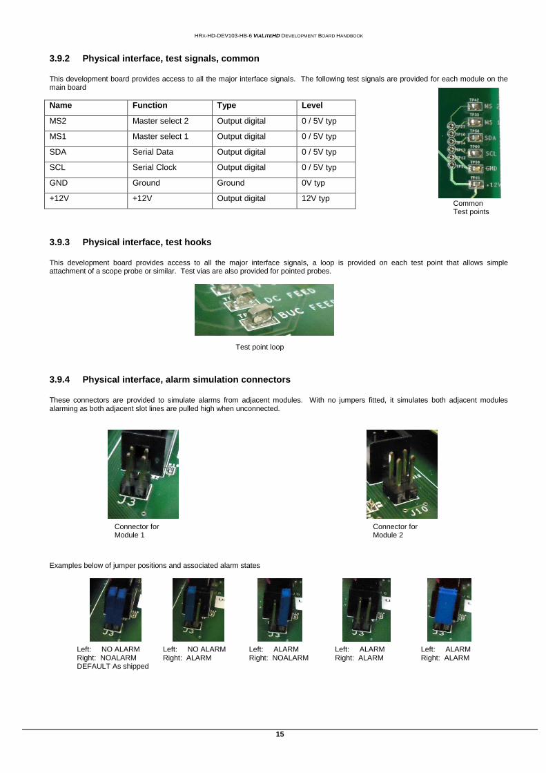
3.9.2 Physical interface, test signals, common
This development board provides access to all the major interface signals. The following test signals are provided for each module on the main board
Name Function Type Level
MS2 Master select 2 Output digital 0 / 5V typ
MS1 Master select 1 Output digital 0 / 5V typ
SDA Serial Data Output digital 0 / 5V typ
SCL Serial Clock Output digital 0 / 5V typ
GND Ground Ground 0V typ
+12V +12V Output digital 12V typ
3.9.3 Physical interface, test hooks
This development board provides access to all the major interface signals, a loop is provided on each test point that allows simple attachment of a scope probe or similar. Test vias are also provided for pointed probes.
3.9.4 Physical interface, alarm simulation connectors
These connectors are provided to simulate alarms from adjacent modules. With no jumpers fitted, it simulates both adjacent modules alarming as both adjacent slot lines are pulled high when unconnected.
Examples below of jumper positions and associated alarm states
Test point loop
Connector for Module 1
Connector for Module 2
Left: ALARM Right: ALARM
Left: NO ALARM Right: ALARM
Left: ALARM Right: NOALARM
Left: NO ALARM Right: NOALARM DEFAULT As shipped
Left: ALARM Right: ALARM
Common Test points
HRX-HD-DEV103-HB-6 VIALITEHD DEVELOPMENT BOARD HANDBOOK
16
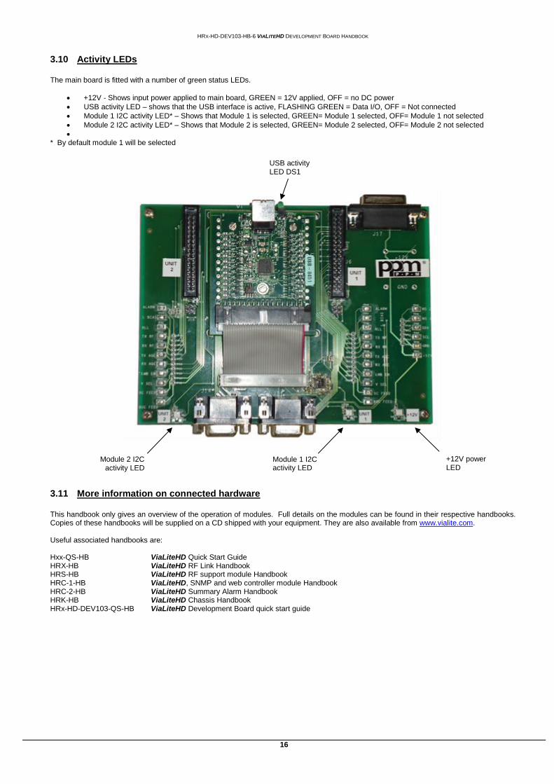
Activity LEDs 3.10
The main board is fitted with a number of green status LEDs.
+12V - Shows input power applied to main board, GREEN = 12V applied, OFF = no DC power
USB activity LED – shows that the USB interface is active, FLASHING GREEN = Data I/O, OFF = Not connected
Module 1 I2C activity LED* – Shows that Module 1 is selected, GREEN= Module 1 selected, OFF= Module 1 not selected
Module 2 I2C activity LED* – Shows that Module 2 is selected, GREEN= Module 2 selected, OFF= Module 2 not selected
* By default module 1 will be selected
More information on connected hardware 3.11
This handbook only gives an overview of the operation of modules. Full details on the modules can be found in their respective handbooks. Copies of these handbooks will be supplied on a CD shipped with your equipment. They are also available from www.vialite.com. Useful associated handbooks are: Hxx-QS-HB ViaLiteHD Quick Start Guide HRX-HB ViaLiteHD RF Link Handbook HRS-HB ViaLiteHD RF support module Handbook HRC-1-HB ViaLiteHD, SNMP and web controller module Handbook HRC-2-HB ViaLiteHD Summary Alarm Handbook HRK-HB ViaLiteHD Chassis Handbook HRx-HD-DEV103-QS-HB ViaLiteHD Development Board quick start guide
USB activity LED DS1
+12V power LED
Module 1 I2C activity LED
Module 2 I2C activity LED
HRX-HD-DEV103-HB-6 VIALITEHD DEVELOPMENT BOARD HANDBOOK
17
4 Software
Starting the program 4.1
To start the software, simply navigate to the “HD Dev kit” icon and <double click>. The default path is START> ALL PROGRAMS > PPM > HD DEV KIT You can also <click> the program ICON
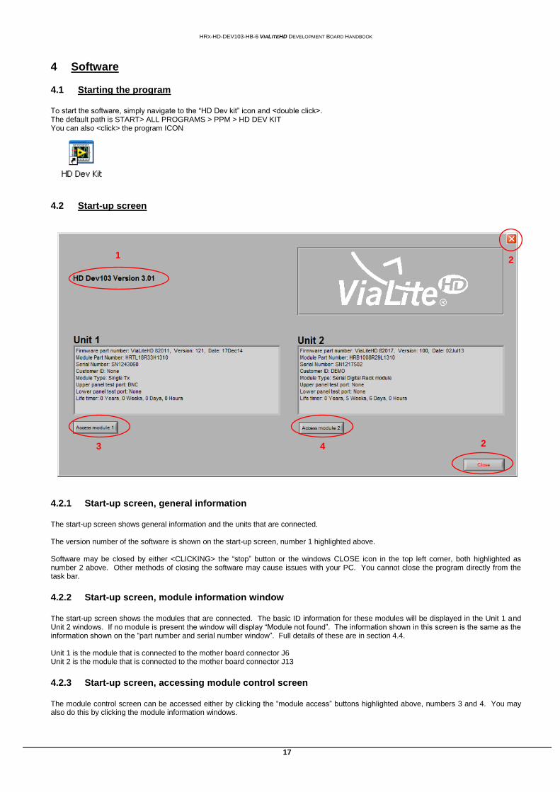
Start-up screen 4.2
4.2.1 Start-up screen, general information
The start-up screen shows general information and the units that are connected. The version number of the software is shown on the start-up screen, number 1 highlighted above. Software may be closed by either <CLICKING> the “stop” button or the windows CLOSE icon in the top left corner, both highlighted as number 2 above. Other methods of closing the software may cause issues with your PC. You cannot close the program directly from the task bar.
4.2.2 Start-up screen, module information window
The start-up screen shows the modules that are connected. The basic ID information for these modules will be displayed in the Unit 1 and Unit 2 windows. If no module is present the window will display “Module not found”. The information shown in this screen is the same as the information shown on the “part number and serial number window”. Full details of these are in section 4.4. Unit 1 is the module that is connected to the mother board connector J6 Unit 2 is the module that is connected to the mother board connector J13
4.2.3 Start-up screen, accessing module control screen
The module control screen can be accessed either by clicking the “module access” buttons highlighted above, numbers 3 and 4. You may also do this by clicking the module information windows.
1 2
2 4 3
HRX-HD-DEV103-HB-6 VIALITEHD DEVELOPMENT BOARD HANDBOOK
18
Control screen, general 4.3
4.3.1 Control screen, general, information panel
Information panels are shown for each module that provides information on the COMMON part and serial number data, configuration, monitor and alarm for each functional block
4.3.2 Control screen, general, panel LED colours
All ALARM lights are VERY DARK RED (unlit) for INACTIVE or RED (lit) for active All STATUS lights are VERY DARK GREEN (unlit) for INACTIVE or GREEN (lit) for active
4.3.3 Control screen, general, configuration control buttons
The configuration control buttons can be used to toggle the status of various lines. The buttons should be clicked only once, the button will flash to give the USER visual feedback. As the commands are buffered and fed to the modules clicking them twice will have no net effect. The modules status is updated approximately once a second. The FSK DIS and GPS MODE will only work for modules that have these functions. Modules without these functions do not care what their status is.
4.3.4 Control screen, general, gain adjustment
Control screen, general, gain adjustment, gain control priorities 4.3.4.1
There are a number of methods by which the gain may be controlled depending on module type. It is possible to make a number of them active simultaneously. In this case the module firmware will discriminate by order of priority. Highest Priority MGC, manual gain control set using module hardware switches, available on chassis modules SGC, soft gain control, set via controller AGC, Automatic gain control, set via controller Lowest Priority Default gain, Factory pre-set gain The gain set by MGC is not reported through the control interface
Control screen, general, gain adjustment, AGC mode for RX functions 4.3.4.2
The AGC MODE is used on the receiver function to select AGC controlled by either RLL (received light level) or RF power. The LED is used to indicate which of these is selected AGC MODE, LED status GREEN RLL mode selected OFF RF mode selected
Control screen, general, gain adjustment, soft gain control 4.3.4.3
The module can be soft gain controlled using the following steps.
Ensure that the SGC status LED in the status panel is illuminated o If not <CLICK> the <SGC> button in the configuration control panel ONCE o The SGC status LED should illuminate after approximately 1 second o You may now use SGC on this module o It is good practice to toggle the AGC OFF
In the gain adjustment screen <TYPE> in the desired gain o Hovering over the window will show the valid gain range
<CLICK> the <Apply Soft gain> button
The gain will be updated in approximately 2 seconds o This can be verified by checking the RF gain in the Monitor and alarm window
Note: Check that the modules DIP switches are not set to MGC ON
Control screen, general, gain adjustment, automatic gain control 4.3.4.4
AGC gain control can be set using the following steps.
Ensure that the SGC LED is NOT illuminated (as SGC has higher priority) o If not <CLICK> the <SGC> button in the configuration control panel ONCE o The SGC status LED should extinguish after approximately 1 second o You may now AGC control the module
Ensure that the AGC status LED in the status panel is illuminated o If not <CLICK> the <AGC> button in the configuration control panel ONCE o The SGC status LED should illuminate after approximately 1 second o You may now use AGC on this module
HRX-HD-DEV103-HB-6 VIALITEHD DEVELOPMENT BOARD HANDBOOK
19
For RX module ensure that the correct AGC MODE is selected o This mode may be toggled by clicking the <AGC mode> button in the configuration control panel ONCE
In the gain adjustment screen <TYPE> in the desired gain o Hovering over the window will show the valid gain range o The software will not allow you to enter an invalid gain o The module firmware will round the gain to the nearest 0.5dB
<CLICK> the <Apply Soft gain> button
The gain will be updated in approximately 2 seconds o This can be verified by checking the RF gain in the Monitor and alarm window
Note: Check that the module’s DIP switches are not set to MGC ON Check that the module’s SGC is OFF
Control screen, general, gain adjustment, default gain 4.3.4.5
If neither MGC, SGC nor AGC mode is enabled the unit will have its default gain. o This can be verified by checking the RF gain in the Monitor and alarm window
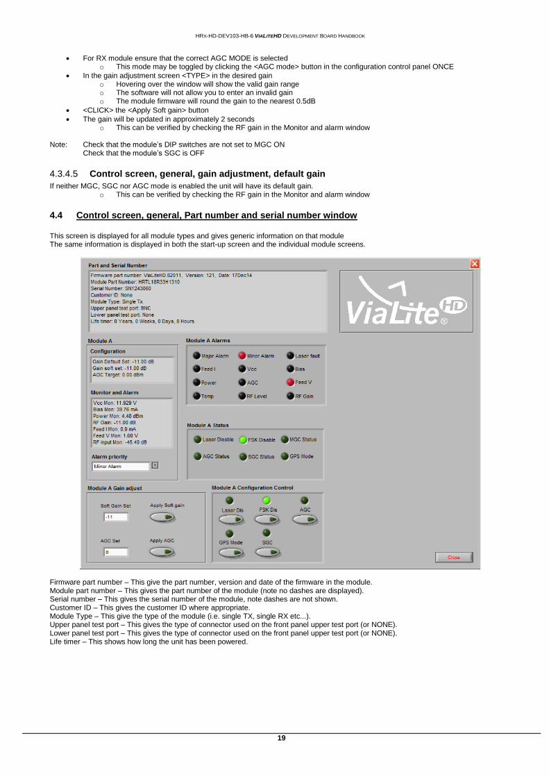
Control screen, general, Part number and serial number window 4.4
This screen is displayed for all module types and gives generic information on that module The same information is displayed in both the start-up screen and the individual module screens.
Firmware part number – This give the part number, version and date of the firmware in the module. Module part number – This gives the part number of the module (note no dashes are displayed). Serial number – This gives the serial number of the module, note dashes are not shown. Customer ID – This gives the customer ID where appropriate. Module Type – This give the type of the module (i.e. single TX, single RX etc...). Upper panel test port – This gives the type of connector used on the front panel upper test port (or NONE). Lower panel test port – This gives the type of connector used on the front panel upper test port (or NONE). Life timer – This shows how long the unit has been powered.
HRX-HD-DEV103-HB-6 VIALITEHD DEVELOPMENT BOARD HANDBOOK
20
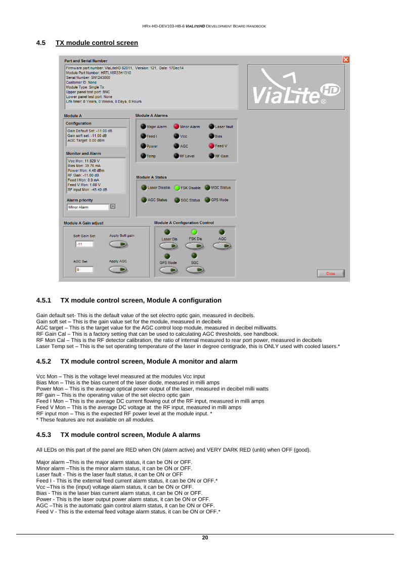
TX module control screen 4.5
4.5.1 TX module control screen, Module A configuration
Gain default set- This is the default value of the set electro optic gain, measured in decibels. Gain soft set – This is the gain value set for the module, measured in decibels AGC target – This is the target value for the AGC control loop module, measured in decibel milliwatts. RF Gain Cal – This is a factory setting that can be used to calculating AGC thresholds, see handbook. RF Mon Cal – This is the RF detector calibration, the ratio of internal measured to rear port power, measured in decibels Laser Temp set – This is the set operating temperature of the laser in degree centigrade, this is ONLY used with cooled lasers.*
4.5.2 TX module control screen, Module A monitor and alarm
Vcc Mon – This is the voltage level measured at the modules Vcc input Bias Mon – This is the bias current of the laser diode, measured in milli amps Power Mon – This is the average optical power output of the laser, measured in decibel milli watts RF gain – This is the operating value of the set electro optic gain Feed I Mon – This is the average DC current flowing out of the RF input, measured in milli amps Feed V Mon – This is the average DC voltage at the RF input, measured in milli amps RF input mon – This is the expected RF power level at the module input. * * These features are not available on all modules.
4.5.3 TX module control screen, Module A alarms
All LEDs on this part of the panel are RED when ON (alarm active) and VERY DARK RED (unlit) when OFF (good). Major alarm –This is the major alarm status, it can be ON or OFF. Minor alarm –This is the minor alarm status, it can be ON or OFF. Laser fault - This is the laser fault status, it can be ON or OFF Feed I - This is the external feed current alarm status, it can be ON or OFF.* Vcc –This is the (input) voltage alarm status, it can be ON or OFF. Bias - This is the laser bias current alarm status, it can be ON or OFF. Power - This is the laser output power alarm status, it can be ON or OFF. AGC –This is the automatic gain control alarm status, it can be ON or OFF. Feed V - This is the external feed voltage alarm status, it can be ON or OFF.*
HRX-HD-DEV103-HB-6 VIALITEHD DEVELOPMENT BOARD HANDBOOK
21
Temp – This is the laser temperature alarm. It is triggered by the TEC control loop status; it can be ON or OFF.* RF Level –This is the RF power level alarm status, it can be ON or OFF.* RF Gain – This is the RF gain alarm status; it can be ON or OFF. * These features are not available on all modules
4.5.4 TX module control screen, Module A status
All LEDs on this part of the panel are GREEN when ON and VERY DARK GREEN (unlit) when OFF. Laser Disable – This is the laser status, the LED indicator is ON (disabled) or OFF (enabled) FSK Disable - This shows if an FSK low speed digital carrier status, the LED indicator is ON (disabled) or OFF (enabled) MGC status – This is the manual gain control status, it can ON or OFF. AGC status – This is the automatic gain control status, it can be ON (enabled) or OFF (disabled). SGC status – This is the software gain control status, it can ON or OFF. GPS mode - This shows the status of the GPS mode, it can be ON (enabled) or OFF (disabled).* * These features are not available on all modules
4.5.5 TX module control screen, Configuration control, buttons
All LEDs on this part of the panel are GREEN when ON and VERY DARK GREEN (unlit) when OFF. The LEDs on the buttons flash as the buttons are actuated, please see noted in section 4.3.3. Laser Dis –This is the laser disable button and is used to toggle the status between ON (disabled) and OFF (enabled). FSK Dis –This is the FSK disable button and is used to toggle the FSK modulator status between ON (disabled) and OFF (enabled). AGC – This is the automatic gain control button and is used to toggle the status between ON (enabled) or OFF (disabled). GPS mode - This is the GPS mode button and is used to toggle the status between ON or OFF. ONLY available for GPS modules.* SGC – This is the software gain control status and is used to toggle the status between ON or OFF. * These features are not available on all modules.
4.5.6 TX module control screen, closing the screen
This window may be closed by either the <CLICKING> “stop” button or the windows CLOSE icon in the top right corner. This will return you to the start-up screen.
HRX-HD-DEV103-HB-6 VIALITEHD DEVELOPMENT BOARD HANDBOOK
22
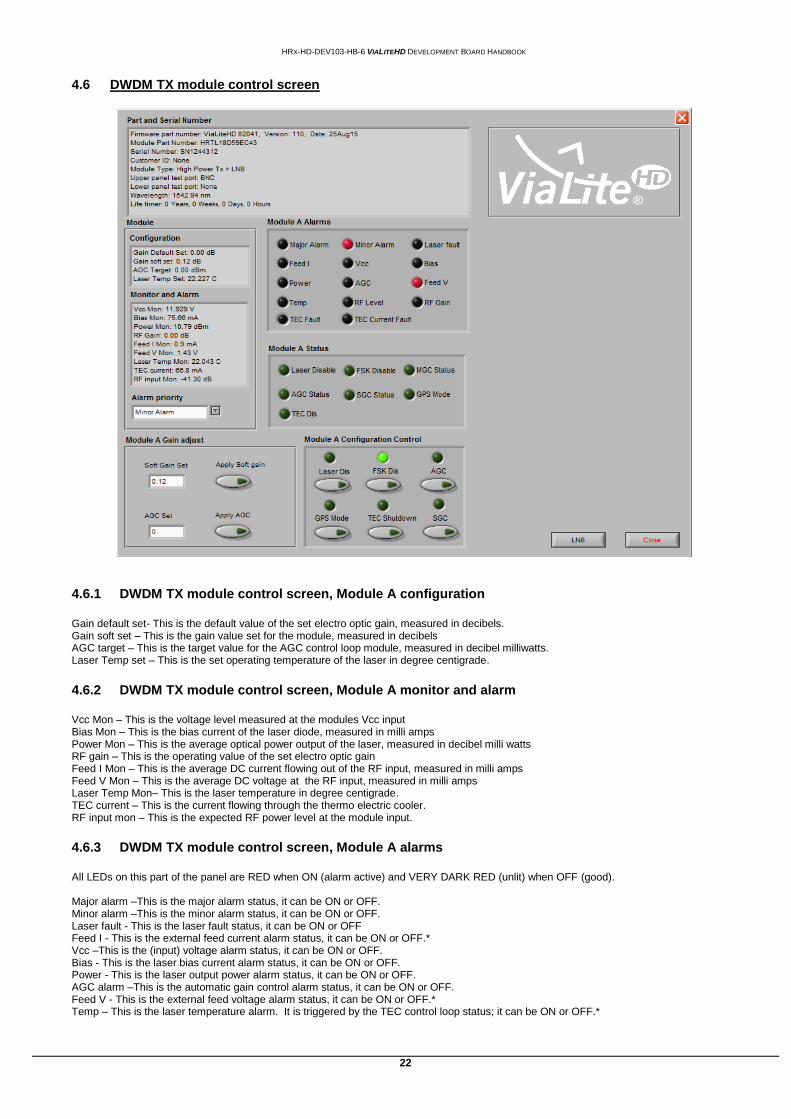
DWDM TX module control screen 4.6
4.6.1 DWDM TX module control screen, Module A configuration
Gain default set- This is the default value of the set electro optic gain, measured in decibels. Gain soft set – This is the gain value set for the module, measured in decibels AGC target – This is the target value for the AGC control loop module, measured in decibel milliwatts. Laser Temp set – This is the set operating temperature of the laser in degree centigrade.
4.6.2 DWDM TX module control screen, Module A monitor and alarm
Vcc Mon – This is the voltage level measured at the modules Vcc input Bias Mon – This is the bias current of the laser diode, measured in milli amps Power Mon – This is the average optical power output of the laser, measured in decibel milli watts RF gain – This is the operating value of the set electro optic gain Feed I Mon – This is the average DC current flowing out of the RF input, measured in milli amps Feed V Mon – This is the average DC voltage at the RF input, measured in milli amps Laser Temp Mon– This is the laser temperature in degree centigrade. TEC current – This is the current flowing through the thermo electric cooler. RF input mon – This is the expected RF power level at the module input.
4.6.3 DWDM TX module control screen, Module A alarms
All LEDs on this part of the panel are RED when ON (alarm active) and VERY DARK RED (unlit) when OFF (good). Major alarm –This is the major alarm status, it can be ON or OFF. Minor alarm –This is the minor alarm status, it can be ON or OFF. Laser fault - This is the laser fault status, it can be ON or OFF Feed I - This is the external feed current alarm status, it can be ON or OFF.* Vcc –This is the (input) voltage alarm status, it can be ON or OFF. Bias - This is the laser bias current alarm status, it can be ON or OFF. Power - This is the laser output power alarm status, it can be ON or OFF. AGC alarm –This is the automatic gain control alarm status, it can be ON or OFF. Feed V - This is the external feed voltage alarm status, it can be ON or OFF.* Temp – This is the laser temperature alarm. It is triggered by the TEC control loop status; it can be ON or OFF.*
HRX-HD-DEV103-HB-6 VIALITEHD DEVELOPMENT BOARD HANDBOOK
23
RF Level –This is the RF power level alarm status, it can be ON or OFF.* RF Gain – This is the RF gain alarm status; it can be ON or OFF. TEC fault – This is the TEC control loop fault status; it can be ON or OFF.* TEC current fault – This is the TEC current fault status trigger by the current being outside of threshold; it can be ON or OFF.* * These features are not available on all modules
4.6.4 DWDM TX module control screen, Module A status
All LEDs on this part of the panel are GREEN when ON and VERY DARK GREEN (unlit) when OFF. Laser disable – This is the laser status, the LED indicator is ON (disabled) or OFF (enabled) FSK disable - This shows if an FSK low speed digital carrier status, the LED indicator is ON (disabled) or OFF (enabled) MGC status – This is the manual gain control status, it can ON or OFF. AGC status – This is the automatic gain control status, it can be ON (enabled) or OFF (disabled). SGC status – This is the software gain control status, it can ON or OFF. GPS mode - This shows the status of the GPS mode, it can be ON (enabled) or OFF (disabled).* TEC dis - This shows the status of the TEC controller, the LED indicator is ON (disabled) or OFF (enabled) * These features are not available on all modules
4.6.5 DWDM TX module control screen, Configuration control, buttons
All LEDs on this part of the panel are GREEN when ON and VERY DARK GREEN (unlit) when OFF. The LEDs on the buttons flash as the buttons are actuated, please see noted in section 4.3.3. Laser Dis –This is the laser disable button and is used to toggle the status between ON (disabled) and OFF (enabled). FSK Dis –This is the FSK disable button and is used to toggle the FSK modulator status between ON (disabled) and OFF (enabled). AGC – This is the automatic gain control button and is used to toggle the status between ON (enabled) or OFF (disabled). GPS mode - This is the GPS mode button and is used to toggle the status between ON or OFF. ONLY available for GPS modules.* TEC shutdown –This TEC shutdown button is used to toggle the status between ON (TEC off) and OFF (TEC on). SGC – This is the software gain control status and is used to toggle the status between ON or OFF.
4.6.6 DWDM TX module control screen, closing the screen
This window may be closed by either the <CLICKING> “stop” button or the windows CLOSE icon in the top right corner. This wil l return you to the start-up screen.
HRX-HD-DEV103-HB-6 VIALITEHD DEVELOPMENT BOARD HANDBOOK
24
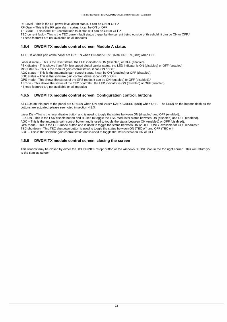
RX module control screen 4.7
4.7.1 RX module control screen, Module A configuration
RLL set – This is the set receive light monitor, the voltage level corresponding to 3mW of laser power. Gain default set- This is the default value of the set electro optic gain, measured in decibels. Gain soft set – This is the gain value set for the module, measured in decibels AGC target – This is the target value for the AGC control loop module, measured in decibel milliwatts.
4.7.2 RX module control screen, Module A monitor and alarm
Vcc Mon – This is the voltage level measured at the modules Vcc input RLL Mon – This is the received light level measured at the modules optical input RF gain – This is the operating value of the set electro optic gain RF output mon – This is the expected RF power level at the module output.* * These features are not available on all modules.
4.7.3 RX module control screen, Module A alarms
All LEDs on this part of the panel are RED when ON (alarm active) and VERY DARK RED (unlit) when OFF (good). Major alarm –This is the major alarm status, it can be ON or OFF. Minor alarm –This is the minor alarm status, it can be ON or OFF. AGC –This is the automatic gain control alarm status, it can be ON or OFF. RF Gain – This is the RF gain alarm status; it can be ON or OFF. Vcc –This is the (input) voltage alarm status, it can be ON or OFF. RLL – This is the received light level alarm status, it can be ON (alarm active) or OFF (good). RF Level –This is the RF power level alarm status, it can be ON or OFF.
HRX-HD-DEV103-HB-6 VIALITEHD DEVELOPMENT BOARD HANDBOOK
25
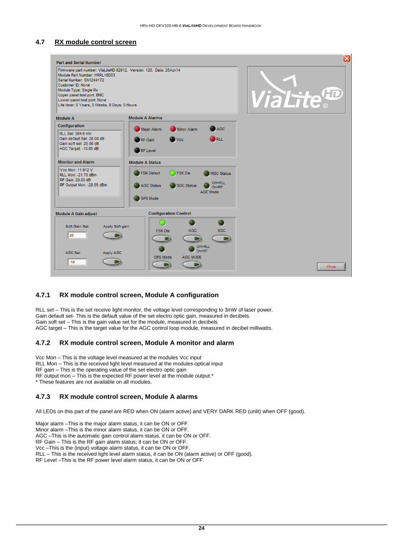
4.7.4 RX module control screen, Module A status
All LEDs on this part of the panel are GREEN when ON and VERY DARK GREEN (unlit) when OFF. FSK detect - This shows if an FSK low speed digital carrier has been detected, it can ON (carrier present) or OFF (no carrier). FSK Dis –This is the frequency shift key digital communications channel status, it can be ON (disabled) or OFF (enabled). MGC status – This is the manual gain control status, it can ON or OFF. AGC status – This is the automatic gain control status, it can be ON (enabled) or OFF (disabled). SGC status – This is the software gain control status, it can ON or OFF. AGC mode - This is the automatic gain control mode, it can be OFF (RLL ) or ON (RF) GPS mode - This shows the status of the GPS mode, it can be ON (enabled) or OFF (disabled), ONLY available for GPS modules.* * These features are not available on all modules.
4.7.5 RX module control screen, Configuration control, buttons
All LEDs on this part of the panel are GREEN when ON and VERY DARK GREEN (unlit) when OFF. The LEDs on the buttons flash as the buttons are actuated, please see noted in paragraph 4.3.3. FSK Dis –This is the FSK disable button and is used to toggle the status between ON (disabled) and OFF (enabled). AGC – This is the automatic gain control button and is used to toggle the status between ON (enabled) or OFF (disabled). SGC – This is the software gain control status and is used to toggle the status between ON or OFF. GPS mode - This is the GPS mode button and is used to toggle the status between ON or OFF. ONLY available for GPS modules.* AGC mode - This is the automatic gain control mode, it can be ON (RF) or OFF (RLL). * These features are not available on all modules.
4.7.6 RX module control screen, closing the screen
This window may be closed by either the <CLICKING> “stop” button or the windows CLOSE icon in the top right corner. This will return you to the start-up screen.
LNB control screen, accessing 4.8
The LNA control screen can be accessed by <CLICKING> the “LNB” button on any transmit module equipped with an internal 13/18V power supply. This is shown in the right of the control screen, see below. This feature is not available on all modules.
HRX-HD-DEV103-HB-6 VIALITEHD DEVELOPMENT BOARD HANDBOOK
26
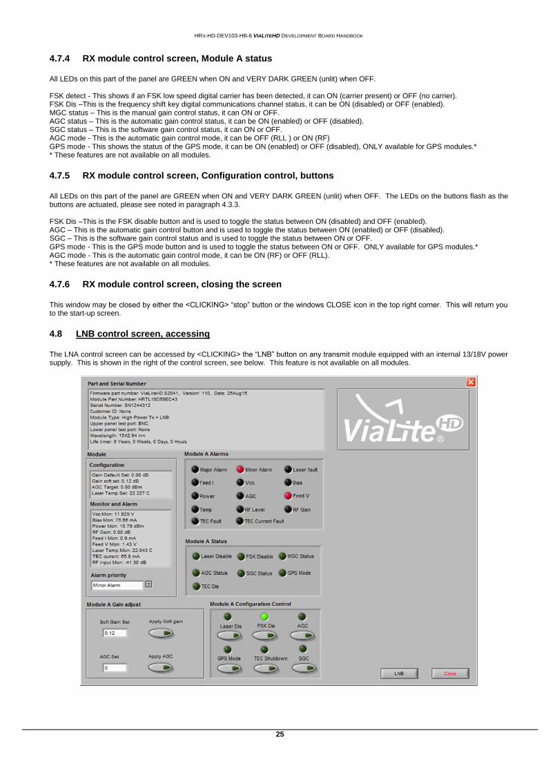
4.8.1 LNB control screen
4.8.2 LNB control screen, alarms
All LEDs on this part of the panel are RED when ON (alarm active) and VERY DARK RED (unlit) when OFF (good). Overload – This is the maximum output current status, it can be ON (alarm active) or OFF (good). Over temperature – This is the over temperature alarm status (of the PSU chip), it can be ON (alarm active) or OFF (good).
4.8.3 LNB control screen, status
All LEDs on this part of the panel are GREEN when ON and VERY DARK GREEN (unlit) when OFF. Power Block Enabled – This shows the power block status, it can be ON (enabled) or OFF (disabled). Output Select – This shows the output voltage selection, it can be OFF (13V nominal) or HIGH (18V nominal). Tone Monitor - This shows the output tone status, it can be ON (22kHz tone) or OFF (no tone). Voltage Monitor – This shows the voltage status, it can be ON (alarm) or OFF (good) Output Current – This shows the output current status, it can be ON (alarm) or OFF (good) Compensation – This shows the cable loss compensation, it can be ON (+1 Volt) or OFF (no extra voltage)
4.8.4 LNB control screen, Configuration control, buttons
All LEDs on this part of the panel are GREEN when ON and VERY DARK GREEN (unlit) when OFF. The LEDs on the buttons flash as the buttons are actuated, please see noted in paragraph 4.3.3. AUX – This toggle auxiliary modes and boost the output voltage, it can be ON (Vout = 22V) or OFF (normal). ITEST – This is the low current threshold, it can be ON (12mA) or OFF (6mA). EN – This is power block enable, it can be ON (power block on) or OFF (power block off). VSEL – This is the output voltage select, it can be ON (18V) or OFF (13V)., LLC – This is the cable loss compensation, it can be ON (voltage output +1V) or OFF (no boost). TEN – This is the tone mode, it can be ON (tone active) or OFF (DSQIN). TTX – This is the tone generator enable, it can be ON (22kHz tone present) or OFF (no tone). PCL – This sets the current limit mode, it can be ON (static) or OFF (pulse) * These features are not available on all modules.
4.8.5 LNA control screen, closing the screen
This window may be closed by either the <CLICKING> “stop” button or the windows CLOSE icon in the top right corner. This wil l return you to the start-up screen.
HRX-HD-DEV103-HB-6 VIALITEHD DEVELOPMENT BOARD HANDBOOK
27
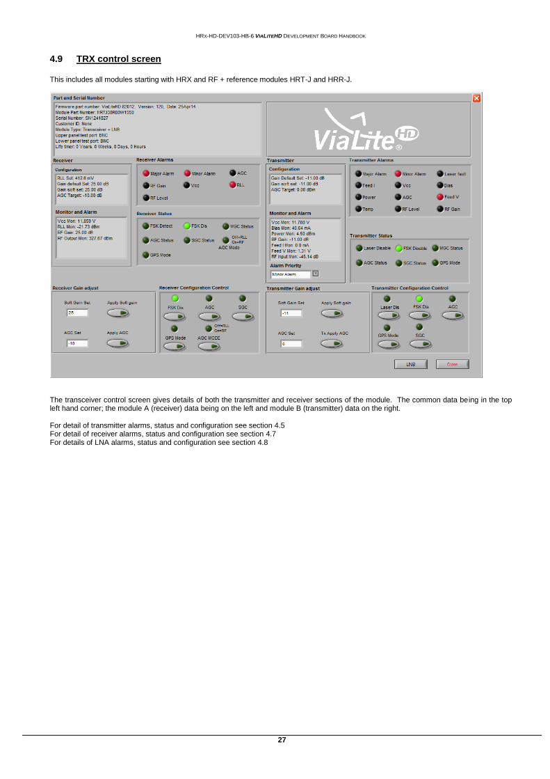
TRX control screen 4.9
This includes all modules starting with HRX and RF + reference modules HRT-J and HRR-J.
The transceiver control screen gives details of both the transmitter and receiver sections of the module. The common data being in the top left hand corner; the module A (receiver) data being on the left and module B (transmitter) data on the right. For detail of transmitter alarms, status and configuration see section 4.5 For detail of receiver alarms, status and configuration see section 4.7 For details of LNA alarms, status and configuration see section 4.8
HRX-HD-DEV103-HB-6 VIALITEHD DEVELOPMENT BOARD HANDBOOK
28
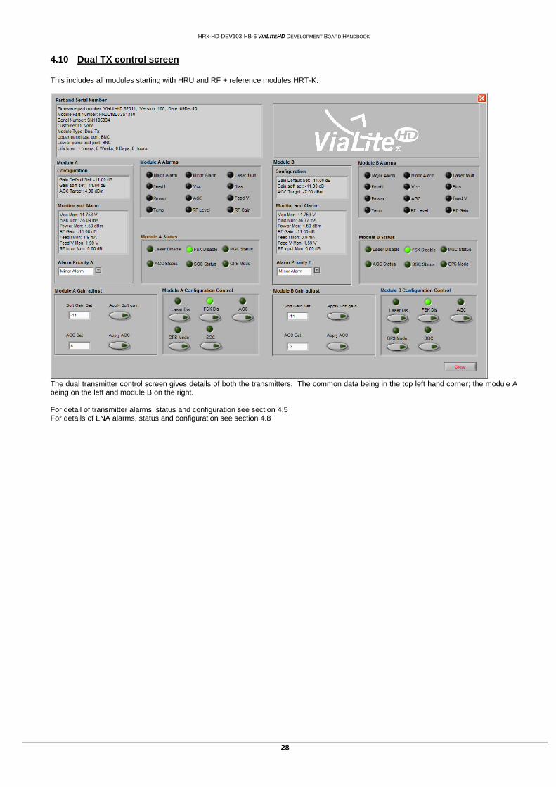
Dual TX control screen 4.10
This includes all modules starting with HRU and RF + reference modules HRT-K.
The dual transmitter control screen gives details of both the transmitters. The common data being in the top left hand corner; the module A being on the left and module B on the right. For detail of transmitter alarms, status and configuration see section 4.5 For details of LNA alarms, status and configuration see section 4.8
HRX-HD-DEV103-HB-6 VIALITEHD DEVELOPMENT BOARD HANDBOOK
29
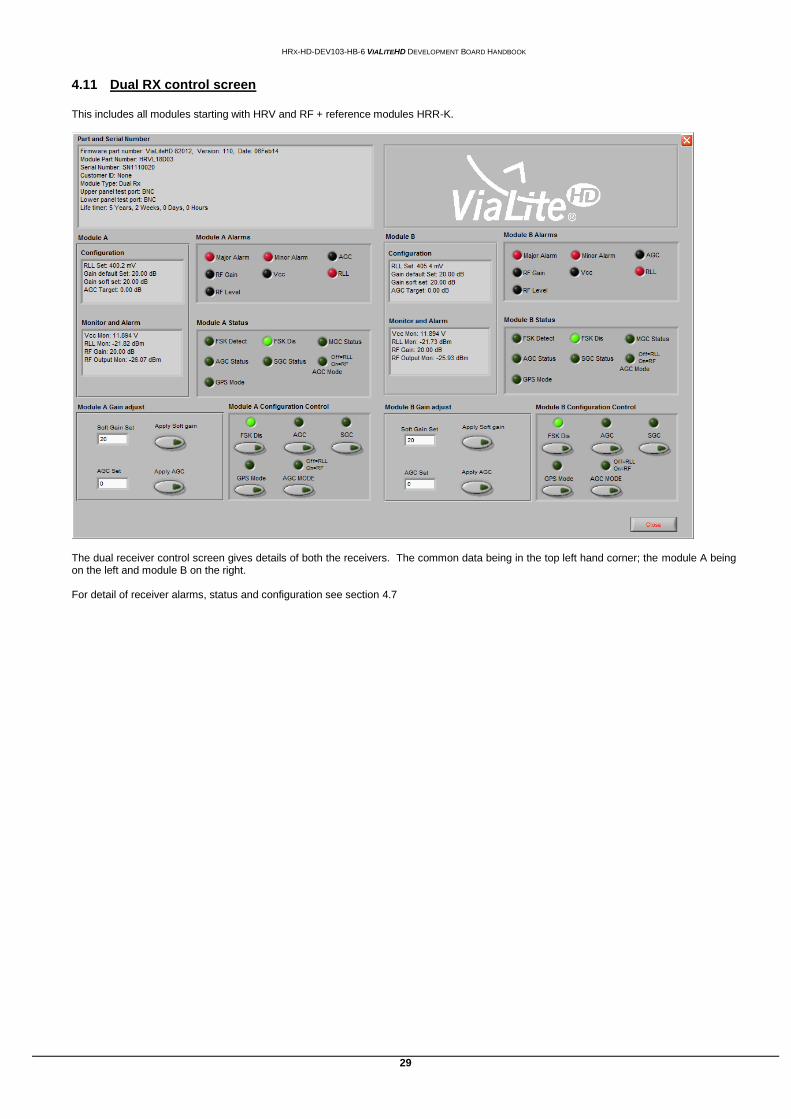
Dual RX control screen 4.11
This includes all modules starting with HRV and RF + reference modules HRR-K.
The dual receiver control screen gives details of both the receivers. The common data being in the top left hand corner; the module A being on the left and module B on the right. For detail of receiver alarms, status and configuration see section 4.7
HRX-HD-DEV103-HB-6 VIALITEHD DEVELOPMENT BOARD HANDBOOK
30
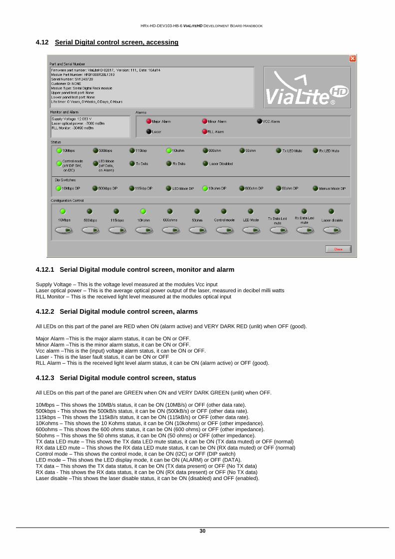
Serial Digital control screen, accessing 4.12
4.12.1 Serial Digital module control screen, monitor and alarm
Supply Voltage – This is the voltage level measured at the modules Vcc input Laser optical power – This is the average optical power output of the laser, measured in decibel milli watts RLL Monitor – This is the received light level measured at the modules optical input
4.12.2 Serial Digital module control screen, alarms
All LEDs on this part of the panel are RED when ON (alarm active) and VERY DARK RED (unlit) when OFF (good). Major Alarm –This is the major alarm status, it can be ON or OFF. Minor Alarm –This is the minor alarm status, it can be ON or OFF. Vcc alarm –This is the (input) voltage alarm status, it can be ON or OFF. Laser - This is the laser fault status, it can be ON or OFF RLL Alarm – This is the received light level alarm status, it can be ON (alarm active) or OFF (good).
4.12.3 Serial Digital module control screen, status
All LEDs on this part of the panel are GREEN when ON and VERY DARK GREEN (unlit) when OFF. 10Mbps – This shows the 10MB/s status, it can be ON (10MB/s) or OFF (other data rate). 500kbps - This shows the 500kB/s status, it can be ON (500kB/s) or OFF (other data rate). 115kbps – This shows the 115kB/s status, it can be ON (115kB/s) or OFF (other data rate). 10Kohms – This shows the 10 Kohms status, it can be ON (10kohms) or OFF (other impedance). 600ohms – This shows the 600 ohms status, it can be ON (600 ohms) or OFF (other impedance). 50ohms – This shows the 50 ohms status, it can be ON (50 ohms) or OFF (other impedance). TX data LED mute – This shows the TX data LED mute status, it can be ON (TX data muted) or OFF (normal) RX data LED mute – This shows the RX data LED mute status, it can be ON (RX data muted) or OFF (normal) Control mode – This shows the control mode, it can be ON (I2C) or OFF (DIP switch) LED mode – This shows the LED display mode, it can be ON (ALARM) or OFF (DATA). TX data – This shows the TX data status, it can be ON (TX data present) or OFF (No TX data) RX data - This shows the RX data status, it can be ON (RX data present) or OFF (No TX data) Laser disable –This shows the laser disable status, it can be ON (disabled) and OFF (enabled).

HRX-HD-DEV103-HB-6 VIALITEHD DEVELOPMENT BOARD HANDBOOK
31
The lower section shows the setting set by the DIP switches, these will be displayed irrespective of the control mode setting (manual/ I2C). There are no DIP switches for either 10Mbps or 10 kohm, these settings are selected if either no other rate/impedance switch is set or if an illegal setting (i.e. DIP switches both selecting 500kBps and 115kBps or both 600 ohms and 50 ohms) is selected. 10Mbps DIP– This shows the 10MB/s DIP switch setting, it can be ON (10MB/s) or OFF (other data rate); no hardware switch 500kbps DIP- This shows the 500kB/s DIP switch setting, it can be ON (500kB/s) or OFF (other data rate). 115kbps DIP – This shows the 115kB/s DIP switch setting, it can be ON (115kB/s) or OFF (other data rate). LED mode DIP – This shows the LED display mode switch setting, it can be ON (ALARM) or OFF (DATA). 10Kohms DIP – This shows the 10 Kohms DIP switch setting, it can be ON (10kohms) or OFF (other impedance); no hardware switch 600ohms DIP – This shows the 600 ohms DIP switch setting, it can be ON (600 ohms) or OFF (other impedance). 50ohms DIP – This shows the 50 ohms DIP switch setting, it can be ON (50 ohms) or OFF (other impedance). Manual Mode – This shows the Manual mode DIP switch setting, it can be ON (DIP switch control) or OFF (I2C/software)
4.12.4 Serial Digital module control screen, Configuration control, buttons
All LEDs on this part of the panel are GREEN when ON and VERY DARK GREEN (unlit) when OFF. The LEDs on the buttons flash as the buttons are actuated, please see noted in section 4.3.3. 10Mbps – This sets the data rate of the module to 10MB/s it can be ON (10MB/s) or OFF (other data rate). 500kbps - This sets the data rate of the module to 500kB/s it can be ON (500kB/s) or OFF (other data rate). 115kbps – This sets the data rate of the module to 115kB/s it can be ON (115kB/s) or OFF (other data rate). Note: ENABLING any data rate button will disable the other data rates 10Kohms – This sets the impedance of the module to 10 Kohms it can be ON (10kohms) or OFF (other impedance). 600ohms - This sets the impedance of the module to 600 ohms it can be ON (600 ohms) or OFF (other impedance). 50ohms – This sets the impedance of the module to 50 ohms it can be ON (50 ohms) or OFF (other impedance). Note: ENABLING any impedance button will disable the other data rates Control mode – This toggles the control mode between I2C software and DIP switch, it can be ON (I2C) or OFF (DIP switch) LED mode – This toggles the LED mode between DATA and ALARM, it can be ON (ALARM) or OFF (DATA). TX data Led mute – This toggles the TX data mute input to the data LED, it can be ON (TX data muted) or OFF (normal) RX data Led mute – This toggles the RX data mute input to the data LED, it can be ON (RX data muted) or OFF (normal) Laser disable – This is the laser disable button and is used to toggle the status between ON (disabled) and OFF (enabled).
4.12.5 Serial Digital module control screen, closing the screen
This window may be closed by either the <CLICKING> “stop” button or the windows CLOSE icon in the top right corner. This wil l return you to the start-up screen.
HRX-HD-DEV103-HB-6 VIALITEHD DEVELOPMENT BOARD HANDBOOK
32
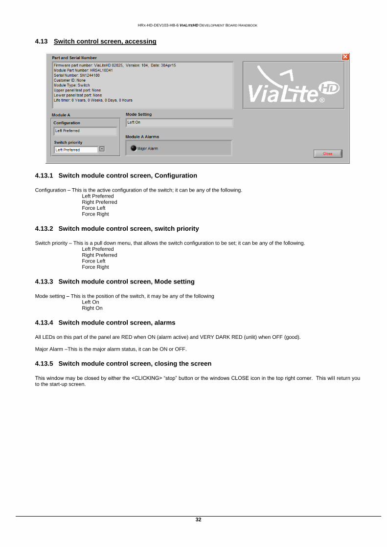
Switch control screen, accessing 4.13
4.13.1 Switch module control screen, Configuration
Configuration – This is the active configuration of the switch; it can be any of the following. Left Preferred Right Preferred Force Left Force Right
4.13.2 Switch module control screen, switch priority
Switch priority – This is a pull down menu, that allows the switch configuration to be set; it can be any of the following. Left Preferred Right Preferred Force Left Force Right
4.13.3 Switch module control screen, Mode setting
Mode setting – This is the position of the switch, it may be any of the following Left On Right On
4.13.4 Switch module control screen, alarms
All LEDs on this part of the panel are RED when ON (alarm active) and VERY DARK RED (unlit) when OFF (good). Major Alarm –This is the major alarm status, it can be ON or OFF.
4.13.5 Switch module control screen, closing the screen
This window may be closed by either the <CLICKING> “stop” button or the windows CLOSE icon in the top right corner. This wil l return you to the start-up screen.
HRX-HD-DEV103-HB-6 VIALITEHD DEVELOPMENT BOARD HANDBOOK
33
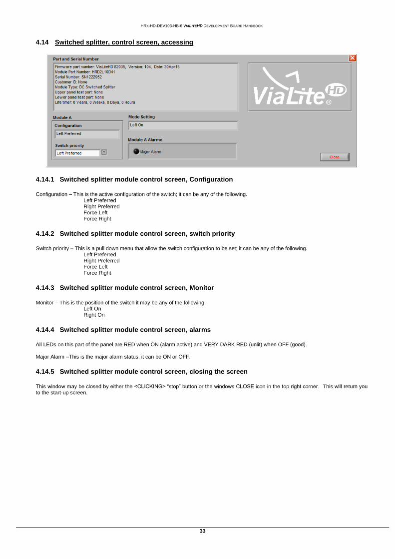
Switched splitter, control screen, accessing 4.14
4.14.1 Switched splitter module control screen, Configuration
Configuration – This is the active configuration of the switch; it can be any of the following. Left Preferred Right Preferred Force Left Force Right
4.14.2 Switched splitter module control screen, switch priority
Switch priority – This is a pull down menu that allow the switch configuration to be set; it can be any of the following. Left Preferred Right Preferred Force Left Force Right
4.14.3 Switched splitter module control screen, Monitor
Monitor – This is the position of the switch it may be any of the following Left On Right On
4.14.4 Switched splitter module control screen, alarms
All LEDs on this part of the panel are RED when ON (alarm active) and VERY DARK RED (unlit) when OFF (good). Major Alarm –This is the major alarm status, it can be ON or OFF.
4.14.5 Switched splitter module control screen, closing the screen
This window may be closed by either the <CLICKING> “stop” button or the windows CLOSE icon in the top right corner. This will return you to the start-up screen.
HRX-HD-DEV103-HB-6 VIALITEHD DEVELOPMENT BOARD HANDBOOK
34
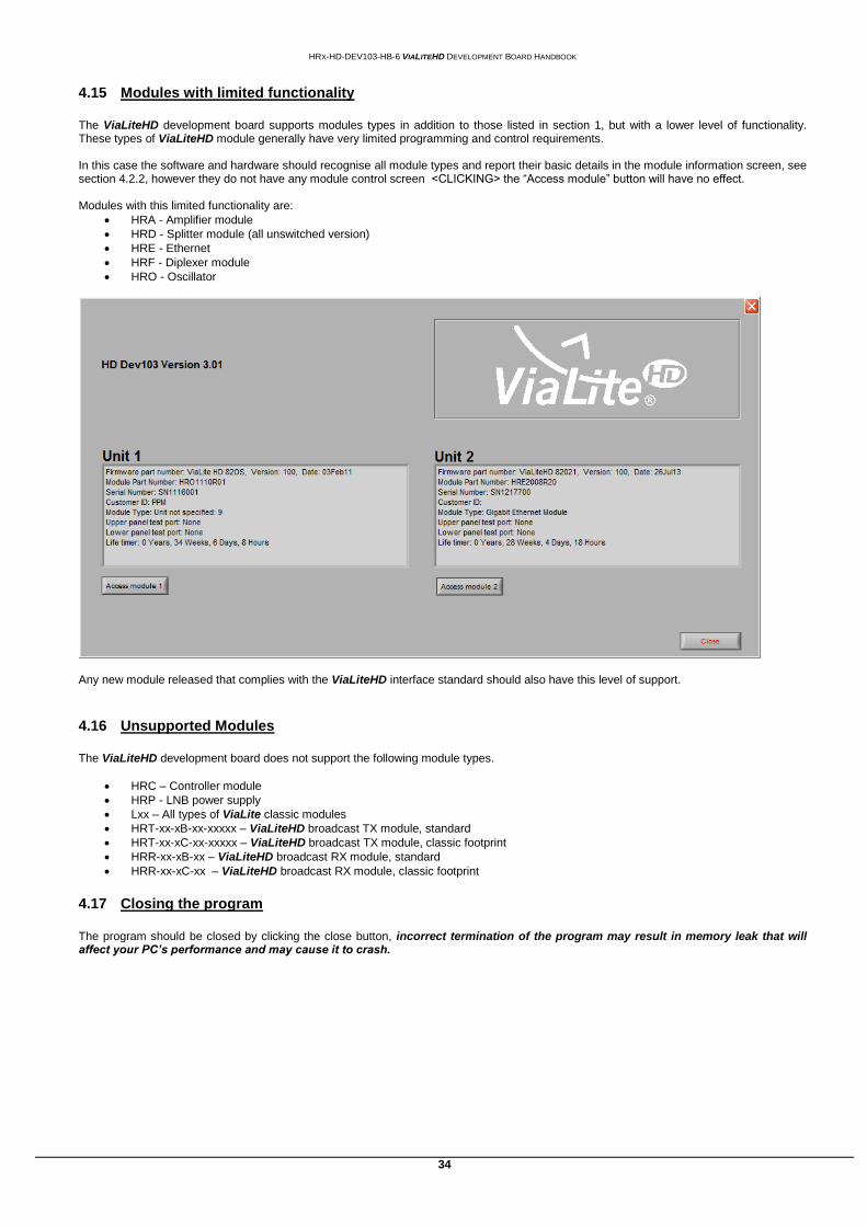
Modules with limited functionality 4.15
The ViaLiteHD development board supports modules types in addition to those listed in section 1, but with a lower level of functionality. These types of ViaLiteHD module generally have very limited programming and control requirements. In this case the software and hardware should recognise all module types and report their basic details in the module information screen, see section 4.2.2, however they do not have any module control screen <CLICKING> the “Access module” button will have no effect. Modules with this limited functionality are:
HRA - Amplifier module
HRD - Splitter module (all unswitched version)
HRE - Ethernet
HRF - Diplexer module
HRO - Oscillator
Any new module released that complies with the ViaLiteHD interface standard should also have this level of support.
Unsupported Modules 4.16
The ViaLiteHD development board does not support the following module types.
HRC – Controller module
HRP - LNB power supply
Lxx – All types of ViaLite classic modules
HRT-xx-xB-xx-xxxxx – ViaLiteHD broadcast TX module, standard
HRT-xx-xC-xx-xxxxx – ViaLiteHD broadcast TX module, classic footprint
HRR-xx-xB-xx – ViaLiteHD broadcast RX module, standard
HRR-xx-xC-xx – ViaLiteHD broadcast RX module, classic footprint
Closing the program 4.17
The program should be closed by clicking the close button, incorrect termination of the program may result in memory leak that will affect your PC’s performance and may cause it to crash.
HRX-HD-DEV103-HB-6 VIALITEHD DEVELOPMENT BOARD HANDBOOK
35
5 Controlling ViaLiteHD module using I2C
When ViaLiteHD modules are configured they will continue operating in their current configuration, even after power cycling. Hence the development board may be used to set up a module. For users who wish to address the modules directly or read memory locations within their own system, the following paragraphs contain all the required details. The OEM and EDGE modules may be addressed directly. The chassis mount and blind mate modules require that their module select line are high to address them, details of the pin outs can be found in the appropriate module handbooks Great care should be taken when controlling the module. All factory calibration and operational code areas are password protected to guard them against accidental erasure.
Example of setting module gain 5.1
For this example we will set the gain of a receiver, using SGC mode. Terms used below relate to I2C maps shown on the following pages.
1. The module in use is an OEM module so it has I2C address of A4 2. Read the value of “Gain soft set min” to determine minimum allowable gain, memory address given in following table 3. Read the value of “Gain soft set max” to determine maximum allowable gain, memory address given in following table
You now have the valid range over which you can control the gain. Any values outside of this range will be trapped by the modules firmware and assigned the nearest valid value. Note: The table the gain is a signed value (i.e. positive or negative) of two bytes, with each unit being 10mdB (0.01dB).
The value of “Gain soft set max” from memory address 0x80 – 0x81 is 0xFF06 is -2.5dB The value of “Gain soft set min” from memory address 0x82 – 0x83 is 0x0514 is +13.0dB
4. Read value of “Gain soft set”, to establish the current gain The value of “Gain soft set” from memory address 0xA4 – 0xA5 is 0x01F4 is +5.0dB Note: This value will only be valid if the module is operating in SGC mode If none of the gain modes is set the unit will have the “Gain default set” value from address 0xA2 – 0xA3
5. Read value of “FSK Dis status”, this will be needed to construct the control byte 6. Read value of “AGC Status” , this will be needed to construct the control byte 7. Read value of “SGC Status” , this will be needed to construct the control byte 8. Read value of “AGC Mode” , this will be needed to construct the control byte 9. Read value of “GPS Mode” , this will be needed to construct the control byte
All the status bits above share a status byte. The value of the status bit from memory address 0xFD read was 0x40, 01000000 This indicates that FSK detect = 0, No signal bit 0 FSK Dis Status= 1, Disabled bit 1 MGC Status = 0, Disabled bit 2 AGC Status = 0, Disabled bit 3 SGC Status = 0, Disabled bit 4 AGC Mode Sel = 0, Disabled bit 5 GPS Mode Sel = 1, Enabled bit 6 Not used bit 7 You now know the current set value of all the other bits required by the control word. This will allow you to write the control word that set the mode of operation and preserve any current set value if desired. The memory address given in following table
10. If the units is not already set into SGC mode write to the memory map to set the module into SGC mode Assuming you wish to change the unit to SGC mode and leave all other parameters as previously: Rx Ctrl: FSK Dis= 1, Disabled bit 0 Rx Ctrl: AGC = 0, Disabled bit 1 Rx Ctrl: SGC = 1 Enabled bit 2 Rx Ctrl: AGC Mode Sel = 0, Disabled bit 3 Rx Ctrl: GPS Mode Sel = 1, Enabled bit 4 Not use bit 5-15 Write the control word to memory address 0xCC – 0xCD this is 00000000 00010100 = 0x0014 See the memory map for the appropriate address
11. Write the new SGC value to “Gain soft set” Assume that you wish to increase the gain by 1dB, from +5dB (read previously) to +6dB Write the control word to “Gain soft set” memory address 0xA4 – 0xA5 with value of 0x0258
12. You have now increased the gain and set the unit into SGC mode
HRX-HD-DEV103-HB-6 VIALITEHD DEVELOPMENT BOARD HANDBOOK
36
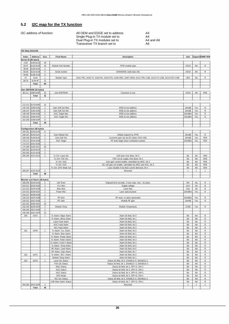
I2C map for the TX function 5.2
I2C address of function: All OEM and EDGE set to address A4 Single Plug-in TX module set to A4 Dual Plug-in TX modules set to A4 and A6 Transceiver TX branch set to A6
Ignis Tx I2C Map (10Jul15)
Index Address Size Field Name Description Unit Signed SNMP R/W
Serial ID (80 bytes)
0-28 0x00-0x1C 29
29-47 0x1D-0x2F 19 Module Part Number PPM module type ASCII NA R
48-49 0x30-0x31 2
50-58 0x32-0x3A 9 Serial number SNXXXXXXX, build date info ASCII NA R
59-66 0x3B-0x42 8
67 0x43 1 Module Type 0x01=TRx, 0x02=Tx, 0x03=Rx, 0x04=DTx, 0x05=DRx, 0x0F=OEM, 0xC1=TRx+LNB, 0xC2=Tx+LNB, 0xC4=DTx+LNB HEX NA R
68-79 0x44-4F 12
Total 80
User EEPROM (32 bytes)
80-111 0X50-0x6F 32 User EEPROM Customer to use ASCII NA R/W
Total 32
112-113 0x70-0x8F 32
144-145 0x90-0x91 2 Gain Soft Set Max MSB at low address 10mdB Yes R
146-147 0x92-0x93 2 Gain Soft Set Min MSB at low address 10mdB Yes R
148-149 0x94-0x95 2 AGC Target Max MSB at low address 10mdBm Yes R
150-151 0x96-0x97 2 AGC Target Min MSB at low address 10mdBm Yes R
152-159 0x98-0x9F 8
Total 48
Configuration (48 bytes)
160-161 0xA0-0xA5 6
166-167 0xA6-0xA7 2 Gain Default Set Default setpoint by PPM 10mdB Yes R
168-169 0xA8-0xA9 2 Gain Soft Set Customer gain set via I2C (when SGC=ON) 10mdB Yes R/W
170-171 0xAA-0xAB 2 AGC Target RF level target (laser modulation power) 10mdBm Yes R/W
172-173 0xAC-0xAD 2
174-199 0xAE-0xC7 26
200-201 0xC8-0xC9 2
202-203 0xCA-0xCB 2
204-205 0xCC-0xCD 2 Tx Ctrl: Laser Dis Soft laser shut down, bit 0 Bit NA R/W
Tx Ctrl: FSK Dis FSK circuit supply shut down, bit 1 Bit NA R/W
Tx Ctrl: AGC Auto gain control enable, overridden by MGC, bit 2 Bit NA R/W
Tx Ctrl: SGC I2C soft gain set enable, overridden by MGC and AGC, bit 3 Bit NA R/W
Tx Ctrl: GPS Mode Sel Laser disable if low feed current detected, bit 4 Bit NA R/W
206-207 0xCE-0xCF 2 Reserved x x x
Total 48
Monitor and Alarm (48 bytes)
208-209 0xD0-0xD1 2 Life Timer Elapsed-time recorder, 2 hour step, max ~15 years 2Hr No R
210-211 0xD2-0xD3 2 Vcc Mon Supply voltage 1mV No R
212-213 0xD4-0xD5 2 Bias Mon Laser bias 2uA No R
214-215 0xD6-0xD7 2 Power Mon Laser optical power 10mdBm Yes R
216-217 0xD8-0xD9 2
218-219 0xDA-0xDB 2 RF Mon RF level, no alarm generated 10mdBm Yes R
220-221 0xDC-0xDD 2 RF Gain Module RF gain 10mdB Yes R
222-231 0xDE-0xE7 10
232-233 0xE8-0xE9 2 Module Temp Module Temperature C/256 Yes R
234-235 0xEA-0xEB 2
235-249 0xEC-0xF9 14
250 0xFA 1 Tx Alarm: Major Alarm Alarm bit field, bit 0 Bit NA R
Tx Alarm: Minor Alarm Alarm bit field, bit 1 Bit NA R
Laser Fault Alarm Alarm bit field, bit 2 Bit NA R
AGC Fault Alarm Alarm bit field, bit 3 Bit NA R
TEC Fault Alarm Alarm bit field, bit 4 Bit NA R
251 0xFB 1 Tx Alarm: Vcc Alarm Alarm bit field, bit 0 Bit NA R
Tx Alarm: Bias Alarm Alarm bit field, bit 1 Bit NA R
Tx Alarm: Power Alarm Alarm bit field, bit 2 Bit NA R
Tx Alarm: Feed I Alarm Alarm bit field, bit 3 Bit NA R
Tx Alarm: Feed V Alarm Alarm bit field, bit 4 Bit NA R
Tx Alarm: Temp Alarm Alarm bit field, bit 5 Bit NA R
RF Alarm: Level Alarm Alarm bit field, bit 6 Bit NA R
RF Alarm: Gain Alarm Alarm bit field, bit 7 Bit NA R
252 0xFC 1 Tx Alarm: TEC I Alarm Alarm bit field, bit 0 Bit NA R
Moduel Temp Alarm Alarm bit field, bit 1 Bit NA R
253 0xFD 1 Laser Dis Status Status bit field, bit 0, ENABLE=0, DISABLE=1 Bit NA R
FSK Dis Status Status bit field, bit 1, ENABLE= 0, DISABLE=1 Bit NA R
MGC Status Status bit field, bit 2, OFF=0, ON=1 Bit NA R
AGC Status Status bit field, bit 3, OFF=0, ON=1 Bit NA R
SGC Status Status bit field, bit 4, OFF=0, ON=1 Bit NA R
GPS Mode Status bit field, bit 5, OFF=0, ON=1 Bit NA R
TEC Dis Status Status bit field, bit 6, ENABLE=0, DISABLE=1 Bit NA R
LNB Main Alarm Status Status bit field, bit 7, OFF=0, ON=1 Bit NA R
254-255 0xFE-0xFF 2 Reserved x x x
Total 48
HRX-HD-DEV103-HB-6 VIALITEHD DEVELOPMENT BOARD HANDBOOK
37
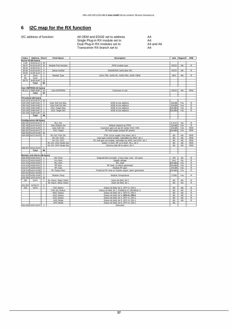
6 I2C map for the RX function
I2C address of function: All OEM and EDGE set to address A4 Single Plug-in RX module set to A4 Dual Plug-in RX modules set to A4 and A6 Transceiver RX branch set to A4
Index Address Size Field Name Description Unit Signed R/W
Seiral ID (80 bytes)
0-28 0x00-0x1C 29
29-47 0x1D-0x2F 19 Module Part Number PPM module type ASCII NA R
48-49 0x30-0x31 2
50-58 0x32-0x3A 9 Serial number SNXXXXXXX, build date info ASCII NA R
59-66 0x3B-0x42 8
67 0x43 1 Module Type 0x01=TRx, 0x03=Rx, 0x05=DRx, 0x0F=OEM HEX NA R
68 0x44 1
69-79 0x45-0x4F 11
Total 80
User EEPROM (32 bytes)
80-111 0X50-0x6F 32 User EEPROM Customer to use ASCII NA R/W
Total 32
Threshold (48 bytes)
112-127 0x70-0x7F 16
128-129 0x80-0x81 2 Gain Soft Set Max MSB at low address 10mdB Yes R
130-131 0x82-0x83 2 Gain Soft Set Min MSB at low address 10mdB Yes R
132-133 0x84-0x85 2 AGC Target Max MSB at low address 10mdBm Yes R
134-135 0x86-0x87 2 AGC Target Min MSB at low address 10mdBm Yes R
136-159 0x88-0x9F 24
Total 48
Configuration (48 bytes)
160-161 0xA0-0xA1 2 RLL Set 0.1mV No R
162-163 0xA2-0xA3 2 Gain Default Set Default setpoint by PPM 10mdB Yes R
164-165 0xA4-0xA5 2 Gain Soft Set Customer gain set via I2C (when SGC=ON) 10mdB Yes R/W
166-167 0xA6-0xA7 2 AGC Target RF level target (output RF power) 10mdBm Yes R/W
168-203 0xA8-0xCB 36
204-205 0xCC-0xCD 2 Rx Ctrl: FSK Dis FSK circuit supply shut down, bit 0 Bit NA R/W
Rx Ctrl: AGC Auto gain control enable, overridden by MGC, bit 1 Bit NA R/W
Rx Ctrl: SGC I2C soft gain set enable, overridden by MGC and AGC, bit 2 Bit NA R/W
Rx Ctrl: AGC Mode Sel Select 1=AGC_RF or 0=AGC_RLL, bit 3 Bit NA R/W
Rx Ctrl: GPS Mode Sel Dummy load off on alarm, bit 4 Bit NA R/W
206-207 0xCE-0xCF 2
Total 48
Monitor and Alarm (48 bytes)
208-209 0xD0-0xD1 2 Life Timer Elapsed-time recorder, 2 hour step, max ~15 years 2Hr No R
210-211 0xD2-0xD3 2 Vcc Mon Supply voltage 1mV No R
212-213 0xD4-0xD5 2 RLL Mon RLL level 10mdBm Yes R
214-215 0xD6-0xD7 2 RF Mon RF level, no alarm generated 10mdBm Yes R
216-217 0xD8-0xD9 2 RF Gain Module RF gain 10mdB Yes R
218-219 0xDA-0xDB 2 RF Output Mon Predicted RF level at module output, alarm generated 10mdBm Yes R
220-221 0xDC-0xDD 2
222-223 0xDE-0xDF 2 Module Temp Module Temperature C/256 Yes R
228-249 0xE0-0xF9 26
250 0xFA 1 Rx Alarm: Major Alarm Alarm bit field, bit 0 Bit NA R
Rx Alarm: Minor Alarm Alarm bit field, bit 1 Bit NA R
251-252 0xFB-FC 2
253 0xFD 1 FSK Detect Status bit field, bit 0, OFF=0, ON=1 Bit NA R
FSK Dis Status Status bit field, bit 1, ENABLE=0, DISABLE=1 Bit NA R
MGC Status Status bit field, bit 2, OFF=0, ON=1 Bit NA R
AGC Status Status bit field, bit 3, OFF=0, ON=1 Bit NA R
SGC Status Status bit field, bit 4, OFF=0, ON=1 Bit NA R
AGC Mode Status bit field, bit 5, OFF=0, ON=1 Bit NA R
GPS Mode Status bit field, bit 6, OFF=0, ON=1 Bit
254-255 0xFE-0xFF 2 Reserved
HRX-HD-DEV103-HB-6 VIALITEHD DEVELOPMENT BOARD HANDBOOK
38
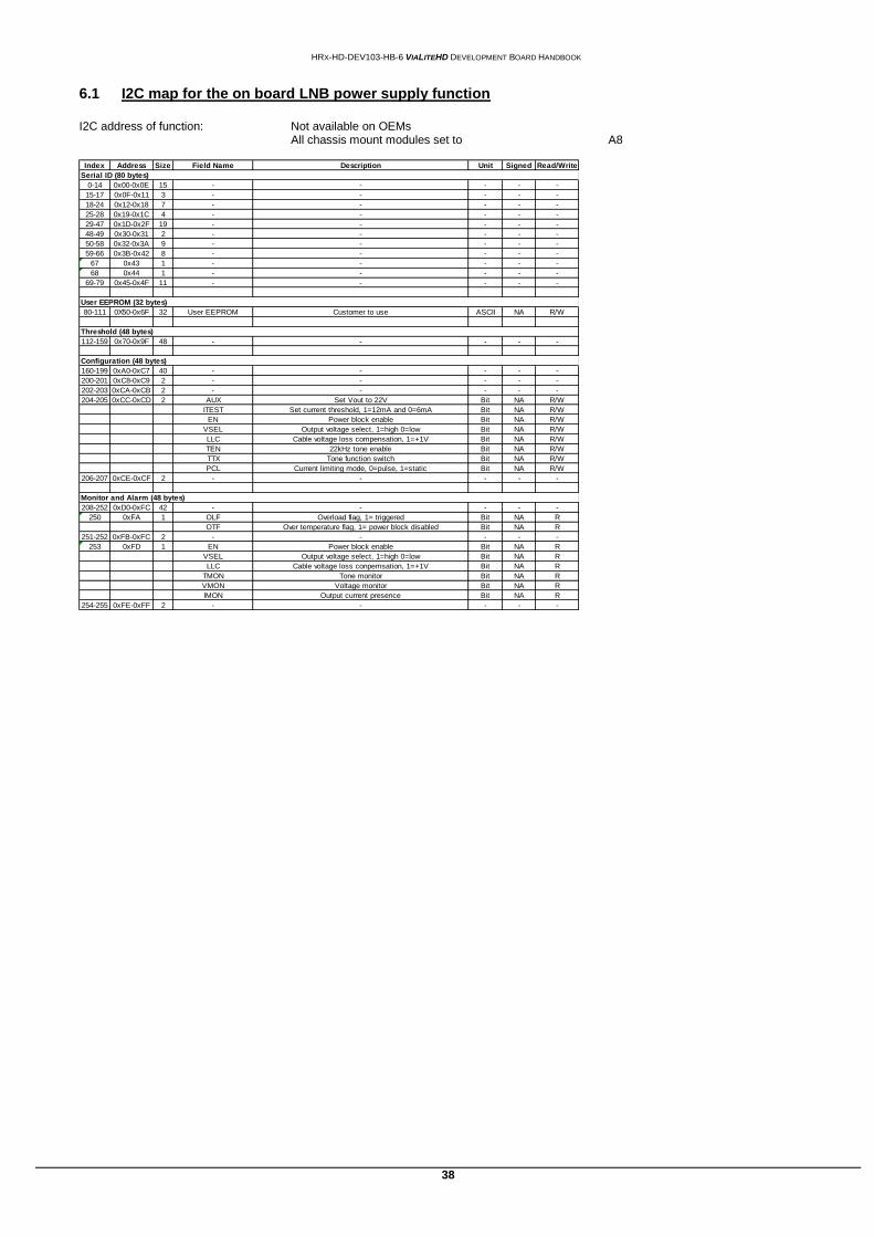
I2C map for the on board LNB power supply function 6.1
I2C address of function: Not available on OEMs All chassis mount modules set to A8
Index Address Size Field Name Description Unit Signed Read/Write
0-14 0x00-0x0E 15 - - - - -
15-17 0x0F-0x11 3 - - - - -
18-24 0x12-0x18 7 - - - - -
25-28 0x19-0x1C 4 - - - - -
29-47 0x1D-0x2F 19 - - - - -
48-49 0x30-0x31 2 - - - - -
50-58 0x32-0x3A 9 - - - - -
59-66 0x3B-0x42 8 - - - - -
67 0x43 1 - - - - -
68 0x44 1 - - - - -
69-79 0x45-0x4F 11 - - - - -
80-111 0X50-0x6F 32 User EEPROM Customer to use ASCII NA R/W
112-159 0x70-0x9F 48 - - - - -
160-199 0xA0-0xC7 40 - - - - -
200-201 0xC8-0xC9 2 - - - - -
202-203 0xCA-0xCB 2 - - - - -
204-205 0xCC-0xCD 2 AUX Set Vout to 22V Bit NA R/W
ITEST Set current threshold, 1=12mA and 0=6mA Bit NA R/W
EN Power block enable Bit NA R/W
VSEL Output voltage select, 1=high 0=low Bit NA R/W
LLC Cable voltage loss compensation, 1=+1V Bit NA R/W
TEN 22kHz tone enable Bit NA R/W
TTX Tone function switch Bit NA R/W
PCL Current limiting mode, 0=pulse, 1=static Bit NA R/W
206-207 0xCE-0xCF 2 - - - - -
208-252 0xD0-0xFC 42 - - - - -
250 0xFA 1 OLF Overload flag, 1= triggered Bit NA R
OTF Over temperature flag, 1= power block disabled Bit NA R
251-252 0xFB-0xFC 2 - - - - -
253 0xFD 1 EN Power block enable Bit NA R
VSEL Output voltage select, 1=high 0=low Bit NA R
LLC Cable voltage loss conpemsation, 1=+1V Bit NA R
TMON Tone monitor Bit NA R
VMON Voltage monitor Bit NA R
IMON Output current presence Bit NA R
254-255 0xFE-0xFF 2 - - - - -
Monitor and Alarm (48 bytes)
Configuration (48 bytes)
Threshold (48 bytes)
Serial ID (80 bytes)
User EEPROM (32 bytes)
HRX-HD-DEV103-HB-6 VIALITEHD DEVELOPMENT BOARD HANDBOOK
39
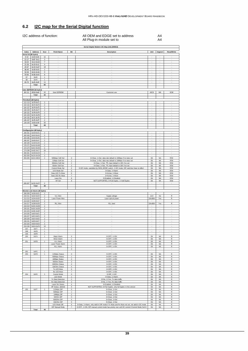
I2C map for the Serial Digital function 6.2
I2C address of function: All OEM and EDGE set to address A4 All Plug-in module set to A4
Index Address Size Field Name Bit Description Unit Signed Read/Write
0-14 0x00-0x0E 15 - - - - -
15-17 0x0F-0x11 3 - - - - -
18-24 0x12-0x18 7 - - - - -
25-28 0x19-0x1C 4 - - - - -
29-47 0x1D-0x2F 19 - - - - -
48-49 0x30-0x31 2 - - - - -
50-58 0x32-0x3A 9 - - - - -
59-66 0x3B-0x42 8 - - - - -
67 0x43 1 - - - - -
68 0x44 1 - - - - -
69-79 0x45-0x4F 11 - - - - -
Total 80
80-111 0X50-0x6F 32 User EEPROM Customer use ASCII NA R/W
Total 32
112-113 0x70-0x71 2 - - - - -
114-115 0x72-0x73 2 - - - - -
116-117 0x74-0x75 2 - - - - -
118-119 0x76-0x77 2 - - - - -
120-121 0x78-0x79 2 - - - - -
122-123 0x7A-0x7B 2 - - - - -
124-125 0c7C-0x7D 2 - - - - -
126-127 0x7E-0x7F 2 - - - - -
128-159 0x80-0x9F 32 - - - - -
Total 48
160-161 0xA0-0xA1 2 - - - - -
162-163 0xA2-0xA3 2 - - - - -
164-165 0xA4-0xA5 2 - - - - -
166-167 0xA6-0xA7 2 - - - - -
168-169 0xA8-0xA9 2 - - - - -
170-171 0xAA-0xAB 2 - - - - -
172-173 0xAC-0xAD 2 - - - - -
174-199 0xAE-0xC7 26 - - - - -
200-201 0xC8-0xC9 2 - - - - -
202-203 0xCA-0xCB 2 - - - - -
204-205 0xCC-0XCD 2 500kbps Soft Set 0 0=Clear, 1=Set, data rate defualt to 10Mbps if no rates set Bit NA R/W
115bps Soft Set 1 0=Clear, 1=Set, data rate defualt to 10Mbps if no rates set Bit NA R/W
600ohm Soft Set 2 0=Clear, 1=Set, TTL input defualt to 10K if no set Bit NA R/W
50ohm Soft Set 3 0=Clear, 1=Set, TTL input defualt to 10K if no set Bit NA R/W
Control Mode Sel 4 0=I2C mode, overidden by MAN_MODE switch, 1=I2C mode, DIP switches have no effect Bit NA R/W
LED Mode Sel 5 0=Data, 1=Alarm Bit NA R/W
Data LED Tx Mute 6 0=Active, 1=Mute Bit NA R/W
Data LED Rx Mute 7 0=Active, 1=Mute Bit NA R/W
Laser Dis 8 0=Enabled, 1=Disabled Bit NA R/W
HF Set 9 NOT SUPPORTED, 0=Full Duplex, 1=Half Duplex Bit NA R/W
206-207 0xCE-0xCF 2 - - - - -
Total 48
208-209 0xD0-0xD1 2 - - - - -
210-211 0xD2-0xD3 2 Vcc Mon Supply voltage 1mV No R
212-213 0xD4-0xD5 2 Laser Power Mon Laser optical power 10mdBm Yes R
214-215 0xD6-0xD7 2 - - - - -
216-217 0xD8-0xD9 2 RLL Mon RLL level 10mdBm Yes R
218-219 0xDA-0xDB 2 - - - - -
220-221 0xDC-0xDD 2 - - - - -
222-223 0xDE-0xDF 2 - - - - -
224-225 0xE0-0xE1 2 - - - - -
226-227 0xE2-0xE3 2 - - - - -
228-229 0xE4-0xE5 2 - - - - -
230-231 0xE6-0xE7 2 - - - - -
232-233 0xE8-0xE9 2 - - - - -
234-246 0xEA-0xF6 13 - - - - -
247 0xF7 1 - - - - -
248 0xF8 1 - - - - -
249 0xF9 1 - - - - -
250 0xFA 1 Major Alarm 0 0=OFF, 1=ON Bit NA R
Minor Alarm 1 0=OFF, 1=ON Bit NA R
251 0xFB 1 Vcc Alarm 0 0=OFF, 1=ON Bit NA R
Laser Power Alarm 1 0=OFF, 1=ON Bit NA R
RLL Alarm 2 0=OFF, 1=ON Bit NA R
- 3 - - - -
252 0xFC 1 - - - - -
253 0xFD 1 115kbps Status 0 0=OFF, 1=ON Bit NA R
500kbps Status 1 0=OFF, 1=ON Bit NA R
10Mbps Status 2 0=OFF, 1=ON Bit NA R
50Ohm Status 3 0=OFF, 1=ON Bit NA R
600Ohm Status 4 0=OFF, 1=ON Bit NA R
10kOhm Status 5 0=OFF, 1=ON Bit NA R
Tx LED Mute 6 0=OFF, 1=ON Bit NA R
Rx LED Mute 7 0=OFF, 1=ON Bit NA R
254 0xFE 1 Control Mode 0 0=DIP, 1=I2C Bit NA R
LED Mode 1 0=Data, 1=Alarm Bit NA R
Tx Data Detection 2 0=No, 1=Yes, Tx data traffic Bit NA R
Rx Data Detection 3 0=No, 1=Yes, Rx data traffic Bit NA R
Laser Dis Status 4 0=Enabled, 1=Disabled Bit NA R
HF Status, deleted 5 NOT SUPPORTED, 0=Full Duplex, only full duplex in this version Bit NA R
255 0xFF 1 115kbps DIP 0 0=Clear, 1=Set Bit NA R
500kbps DIP 1 0=Clear, 1=Set Bit NA R
10Mbps DIP 2 0=Clear, 1=Set Bit NA R
50Ohm DIP 3 0=Clear, 1=Set Bit NA R
600Ohm DIP 4 0=Clear, 1=Set Bit NA R
10kOhm DIP 5 0=Clear, 1=Set Bit NA R
LED Mode DIP 6 0=Data, 1=Alarm, only valid in DIP mode if Tx Mute and Rx Mute not set, not valid in I2C mode Bit NA R
DIP Manual Mode 7 0=OFF, 1=ON, DIP manual control mode has priority over soft I2C control if Control Mode Sel=0 Bit NA R
Total 48
Monitor and Alarm (48 bytes)
Serial Digital Modem I2C Map (A4) (200913)
Seiral ID (80 bytes)
User EEPROM (32 bytes)
Threshold (48 bytes)
Configuration (48 bytes)
HRX-HD-DEV103-HB-6 VIALITEHD DEVELOPMENT BOARD HANDBOOK
40
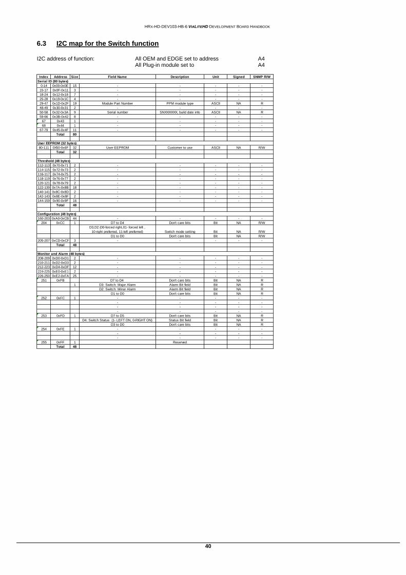
I2C map for the Switch function 6.3
I2C address of function: All OEM and EDGE set to address A4 All Plug-in module set to A4
Index Address Size Field Name Description Unit Signed SNMP R/W
0-14 0x00-0x0E 15 - - - - -
15-17 0x0F-0x11 3 - - - - -
18-24 0x12-0x18 7 - - - - -
25-28 0x19-0x1C 4 - - - - -
29-47 0x1D-0x2F 19 Module Part Number PPM module type ASCII NA R
48-49 0x30-0x31 2 - - - - -
50-58 0x32-0x3A 9 Serial number SNXXXXXXX, build date info ASCII NA R
59-66 0x3B-0x42 8 - - - - -
67 0x43 1 - - - - -
68 0x44 1 - - - - -
67-79 0x45-0x4F 11 - - - - -
Total 80
80-111 0X50-0x6F 32 User EEPROM Customer to use ASCII NA R/W
Total 32
112-113 0x70-0x71 2 - - - - -
114-115 0x72-0x73 2 - - - - -
116-117 0x74-0x75 2 - - - - -
118-119 0x76-0x77 2 - - - - -
120-121 0x78-0x79 2 - - - - -
122-139 0x7A-0x8B 18 - - - - -
140-141 0x8C-0x8D 2 - - - - -
142-143 0x8E-0x8F 2 - - - - -
144-159 0x90-0x9F 16 - - - - -
Total 48
160-203 0xA0-0xCB 44 - - - - -
204 0xCC 1 D7 to D4 Don't care bits Bit NA R/W
D3,D2 (00-forced right,01- forced left ,
10-right preferred, 11-left preferred) Switch mode setting Bit NA R/W
D1 to D0 Don't care bits Bit NA R/W
205-207 0xCD-0xCF 3 - - - - -
Total 48
208-209 0xD0-0xD1 2 - - - - -
210-211 0xD2-0xD3 2 - - - - -
212-223 0xD4-0xDF 12 - - - - -
224-225 0xE0-0xE1 2 - - - - -
226-250 0xE2-0xFA 25 - - - - -
251 0xFB D7 to D4 Don't care bits Bit NA R
1 D3: Switch: Major Alarm Alarm Bit field Bit NA R
D2: Switch: Minor Alarm Alarm Bit field Bit NA R
D1 to D0 Don't care bits Bit NA R
252 0xFC 1 - - - - -
- - - - -
- - - - -
- - - - -
253 0xFD 1 D7 to D5 Don't care bits Bit NA R
D4: Switch Status (1- LEFT ON, 0-RIGHT ON) Status Bit field Bit NA R
D3 to D0 Don't care bits Bit NA R
254 0xFE 1 - - - - -
- - - - -
- - - - -
255 0xFF 1 Reserved
Total 48
Threshold (48 bytes)
Configuration (48 bytes)
Monitor and Alarm (48 bytes)
Serial ID (80 bytes)
User EEPROM (32 bytes)
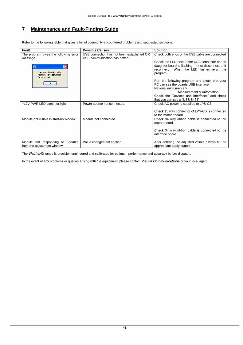
HRX-HD-DEV103-HB-6 VIALITEHD DEVELOPMENT BOARD HANDBOOK
41
7 Maintenance and Fault-Finding Guide
Refer to the following table that gives a list of commonly encountered problems and suggested solutions.
Fault Possible Causes Solution
The program gives the following error message.
USB connection has not been established OR USB communication has halted
Check both ends of the USB cable are connected Check the LED next to the USB connector on the daughter board is flashing. If not disconnect and reconnect. When the LED flashes rerun the program. Run the following program and check that your PC can see the boards USB interface. National instruments > Measurement & Automation Check the “Devices and Interfaces” and check that you can see a “USB-8451”
+12V PWR LED does not light Power source not connected. Check AC power is supplied to LPS-CS Check 15 way connector of LPS-CS is connected to the mother board
Module not visible in start-up window Module not connected Check 34 way ribbon cable is connected to the motherboard Check 34 way ribbon cable is connected to the interface board
Module not responding to updates from the adjustment window
Value changes not applied After entering the adjusted values always hit the appropriate apply button
The ViaLiteHD range is precision engineered and calibrated for optimum performance and accuracy before dispatch. In the event of any problems or queries arising with the equipment, please contact ViaLite Communications or your local agent.
HRX-HD-DEV103-HB-6 VIALITEHD DEVELOPMENT BOARD HANDBOOK
42
8 Glossary
A Ampere AGC Automatic gain control BUC Block up converter CNR Carrier to noise ratio COM Common dB Decibel dBc Decibel relative to carrier dBm Decibel milli watt DC Direct current DHCP Dynamic host configuration Protocol DVB Digital video broadcast DVB-T Digital video broadcast terrestrial FC/APC Fibre connector angled polished contact FC/PC Fibre connector physical contact FOL Fibre optic link FSK Frequency shift keying FTP File transfer protocol g Gram GHz Giga hertz GPS Global positioning system GRN Goods Return Number GUI Graphical user interface HRK3 ViaLiteHD 3U chassis HTML Hypertext mark-up language HP Rack hole pitch measurement of width 5.08mm Hz Hertz I2C Inter-Integrated circuit bus IMD Intermodulation distortion ratio IP Internet protocol IP3 Third order intercept point kg Kilo gram kHz Kilo hertz LAN Local area network LASER Light amplification by stimulated emission of radiation LC/PC Lucent connector physical contact LED Light emitting diode LNA Low noise amplifier LNB Low noise block m Metre mA Milli ampere Max Maximum MGC Manual Gain control MHz Mega hertz Min Minimum mm Milli metre mV Milli volt NC Normally closed NF Noise figure nm Nano meter NO Normally open P1dB Power at one decibel gain compression PC Personal computer PPM Pulse Power and Measurement Ltd PWR Power RF Radio frequency RLL Received light level RST Reset RX Receiver SC/APC Subscriber connector angled polished contact SC/PC Subscriber connector physical contact SFDR Spurious free dynamic range SGC Software gain control SINAD Signal to noise and distortion ratio SNMP Simple network management protocol TEC Thermo electric cooler TCP/IP Transmission Control Protocol TRX Transceiver TX Transmitter Typ Typical VSEL Voltage select VSWR Voltage standing wave ratio W Watt
HRX-HD-DEV103-HB-6 VIALITEHD DEVELOPMENT BOARD HANDBOOK
43
9 Product Warranty
ViaLite Communications guarantees its products, and will maintain them for a period of three years from the date of shipment and at no cost to the customer. Extended warranty options are available at the time of purchase. Please note that the customer is responsible for shipping costs to return the module to ViaLite Communications. ViaLite Communications or its agents will maintain its products in full working order and make all necessary adjustments and parts replacements during the Company’s normal working hours provided that the Customer will pay at the rates currently charged by the Company for any replacements made necessary by accident, misuse, neglect, wilful act or default or any cause other than normal use. Claims must be made promptly, and during the guarantee period. IMPORTANT: - Please contact both your selling agent and ViaLite Communications prior to returning any goods for Warranty or Non-Warranty repairs. Goods will not be accepted without a valid returned merchandise authorisation (RMA) number.
HRX-HD-DEV103-HB-6 VIALITEHD DEVELOPMENT BOARD HANDBOOK
44
10 FCC Approval
Information to the user of ViaLiteHD products. For a Class A digital device or peripheral, the following instructions are furnished to the user. This equipment has been tested and found to comply with the limits for a Class A digital device, pursuant to part 15 of the FCC Rules. These limits are designed to provide reasonable protection against harmful interference when the equipment is operated in a commercial environment. This equipment generates, uses, and can radiate radio frequency energy and, if not installed and used in accordance with the instruction manual, may cause harmful interference to radio communications. Operation of this equipment in a residential area is likely to cause harmful interference in which case the user will be required to correct the interference at his own expense.
PULSE POWER & MEASUREMENT LTD 2015.
NO PART OF THIS DOCUMENT MAY BE REPRODUCED OR TRANSMITTED IN ANY FORM WITHOUT PRIOR WRITTEN PERMISSION.
PULSE POWER & MEASUREMENT LTD, 65 SHRIVENHAM HUNDRED BUSINESS PARK, SWINDON, SN6 8TY, UK. TEL: +44 1793 784389 FAX: +44 1793 784391
EMAIL: [email protected] WEBSITE : WWW.VIALITE.COM