Embed Size (px)
Citation preview

VIA Technical Report No. 31
VIA ELECTRONICS DRAFTING MANUAL
D. Weber, R. Runyon T. Cote, L. Carlisle
February 1978

TABLE OF CONTENTS
1.0 INTRODUCTION............................................... 1-11.1 Construction........................................... 1-11.2 Maintenance........................................... 1-21.3 Configuration and Construction Data Records............ 1-2
2.0 CLASSES OF DRAWINGS AND USAGE............................... 2-12.1 VLA Sketches.......................................... 2-12.2 VLA Drawings........................................... 2-12.3 Vendors' and Contractors' Drawings..................... 2-12.4 Specification Control Drawings......................... 2-12.5 Dummy Drawings.................. ...................... 2-22.6 Altered Item Drawings.................................. 2-22.7 Make From Drawings....................... ... ......... 2-2
2.8 Process Drawings....................... ............... 2-22.9 Test Specifications and Test Procedures............... . 2-22.10 Specifications............. .......................... 2-2
3.0 VLA DRAWING NUMBERING SYSTEMS........................... . 3-14.0 VLA DRAWING TYPES...........................................4-1
4.1 Assembly Drawings..................... ....... ........ 4-14.2 Bill of Materials..................... ................ 4-14.3 Schematic Diagrams.................... ................ 4-14.4 Logic Diagrams................................ ........ 4-2
4.5 Printed Circuit Board Masters....................... .. 4-24.6 Printed Circuit Board Mechanical Drawings.............. 4-24.7 Silkscreen Masters..................................... 4-24.8 Block Diagrams......................................... 4-24.9 Wire Lists............................................ 4-34.10 Mechanical or Miscellaneous Parts..................... 4-3
4.11 Tool Drawings......................................... 4-34.12 Data Lists............................................ 4-3
5.0 DRAWING STRUCTURE........................................... 5-16.0 FORMS AND FORMAT CONVENTIONS............ ................... 6-1
i

7.0 DRAWING PROCEDURES...........................................7-17.1 Drawing Control.........................................7-17.2 Change Orders and Procedures............... ........... .7-17.3 Drawing Revisions.......................................7-27.4 New Designs................. .......................... 7-37.5 Model Documentation.....................................7-57.6 Drawing Checks.................. ...................... .7-67.7 VLA/CV Drafting Liaison..... — .......... ........ .... 7-67.8 VLA Print Library.......................................7-77.9 Drawing Number Assignments............................. .7-77.10 VLA Drawing Number/Title Lists........................ .7-77.11 Drawing Priority................................... ... 7-8
8.0 DRAFTING CONVENTIONS........................................8-18.1 General Requirements....................................8-18.2 Notes on Drawings...................................... 8-58.3 Marking............................................... .8-68.4 Revisions of Drawings and Lists........................ .8-78.5 Dimensioning and Tolerancing.................... ...... 8-88.6 Electrical Component Parts............................ ..8-148.7 Schematic and Logic Diagrams and Interconnections__..... 8-158.8 Wiring Harness and Cable Assembly Drawings..............8-228.9 Linework and Lettering................................. .8-27
9.0 VLA DOCUMENTATION/DRAWING SPECIFICATIONS.................... 9-19.1 VLA Specifications......................................9-19.2 Module Type/Name List................. ................ .9-189.3 Plug In Wire Wrap Board Conventions.................... .9-219.4 Monitor and Control System Notational Conventions........9-299.5 Drawing Listing and Parts Listing Coding Forms...........9-309.6 Standard AMP Connector Components and Tools.............9 -439.7 Basic Module Components............... ................ .9-479.8 Graphic Electrical/ Electronic and Logic Symbols.........9—499.9 Dimensioning and Tolerancing........................... .9-499.10 Miscellaneous Specifications.......................... .9-49
ii
1.0 INTRODUCTIONThis manual describes the drafting practices recommended for VLA
Electronics drawings and is addressed to the draftsmen, technicians and engineers who may be concerned with generating or using these drawings. The emphasis in this manual is to highlight or outline the more important aspects of good documentation procedures; detailed treatment of subjects like symbology, line widths, etc. are beyond the scope of this manual. The draftsmen who generate the drawings are expected to be knowledgeable as to the appropriate practices to be used.
The drafting practices and procedures- set forth in this manual are not new to VLA but have been used by both CV and VLA site draftsmen for some time. This manual is written to formalize these procedures and to serve as a drafting reference for the engineers, technicians and draftsmen.
Drawings are a form of graphic communication and cure generated by VLA drafting for three purposes:
1•1 Construction by contractors and in-house at VLA and Charlottesville. When used for contract construction the drawings must adequately define the end product or we suffer the consequences in the form of poor quality and performance. Correcting contractors' fabrication deficiencies costs time, man-hours and materials at NRAO. It can be very difficult to convince a contractor to upgrade the quality of his work if he can show that he "built it to the print". Contract fabricators have a narrow profit margin and are primarily interested in doing the job within the contract funds so you can expect them to perform the work in the quickest way possible which may not be consistent with our fabrication expectations. Our principle leverage on the contractor is to insist on conformance to the drawings and specifications.
Drawings for in-house built equipment should be just as comprehensive as those for outside contractors' use; don't assume that since an item is being fabricated/built by NRAO "It'll be done right."
1-1
If any features of a design are important to fit, function or quality then they should be put on a drawing to explicitly communicate these requirements to the construction people? if you don't do this, you are delegating the implementation, quality and workmanship decisions to the judgement of the assembly workers. Obviously, verbal directions can be used as an alternate to graphic communication, but people quit, change jobs and forget the directions and special instructions after*a little while. Make adequate drawings!
1.2 Maintenance - It is vitally important that the drawings also contain maintenance oriented information to assist maintenance people in testing, fault isolating and aligning equipment.The engineers and technicians are expected to suggest the appropriate information to the draftsmen as the drawings are generated.
1.3 Configuration and Construction Data Records - The potential for configuration confusion is apparent if we considerthe numbers pertaining to the VLA modules which probably account for the major portion of VLA Electronics drawings. With our 28 antennas (hopefully identical) we use about 50 module types, each of which can have several model variations and revisions within the model. These modules will have been built over several years by a number of contractors and in- house peoplt. If we don't establish and maintain good configuration control data in the form of drawings and wire lists, we will find that maintenance and future modifications will be difficult.
Even one of a kind items should have documentation adequate for maintenance or modification at some future date. For example, we have a Control Building and probably will never
1-2

discard it and replace it with another, but we have kept the construction drawings for use in making changes, running cables and pipes, etc.
This manual also includes a collection of specifications and useful drafting-related information such as drawing number practices, standard electrical and mechanical hardware items and the basic module metal and plastic part numbers.
1-3


2.0 CLASSES OF DRAWINGS AND USAGE
2.1 VLA SketchesVLA sketches are usually informal and quickly drawn for in-
house use but may be quite adequate for contract use. A sketch number (provided by drafting), title and designer’s name are all the formal requirements. It is generally preferable to apply a transfer title block for uniformity of format. VLA sketches should always be drawn on reproducible paper and stored with the drawing files.
2.2 VLA DrawingsVLA drawings are used to define all the hardware features
of the VLA system and consist of a wide variety of types. These types will be described in Section 4 of this manual.
2.3 Vendors* and Contractors* DrawingsWe use a great many purchased items— both commercial and
specially designed. Whenever possible, one or more sets of reproducible drawings for these items should be stored in the drafting files for general reference.
2.4 Specification Control DrawingsSpecification control drawings are a powerful tool in con
trolling critical features of items purchased from contractors.A specification control drawing cites all features on a contractor's drawing which are critical in form, fit or function. Non-critical aspects are left to the contractor’s design and change discretion. The specification control drawing should cite the contractor's name, drawing number, revision level and release/revision date.
2-1
2.5 Dummy DrawingsDummy drawings are sometimes used as linkages or may be used
to reserve some future drawing expansion.
2.6 Altered Item DrawingsAltered item drawings depict changes to purchased items to
make them suitable for our use. Generally, they are based upon a contractor*s drawing.
2.7 Make From DrawingsMake from drawings are drawings that depict changes to an
item to adapt it for a particular function. In general, a make from drawing contains only the information required to implement the specific change to the basic unit. An example of a make from drawing is a VLA Data Set front panel which is "made from" the basic IUA module front panel. Make from drawings, when properly used, can save a lot of drafting time.
2.8 Process DrawingsProcess drawings are a form of graphic specification which
defines some aspect of fabrication, construction or assembly.
2.9 Test Specifications and Test ProceduresTest specifications and test procedures are analogous to
drawings and should be subject to the same configuration control procedure as drawings. These are originated by technicians and engineers and are filed in the site technical files.
2.10 SpecificationsSpecifications are also analagous to drawings and are a
written definition of a product. Specifications and the associated drawings should be cross-referenced. These are originated by engineers and technicians and are filed in the site technical files.
2-2
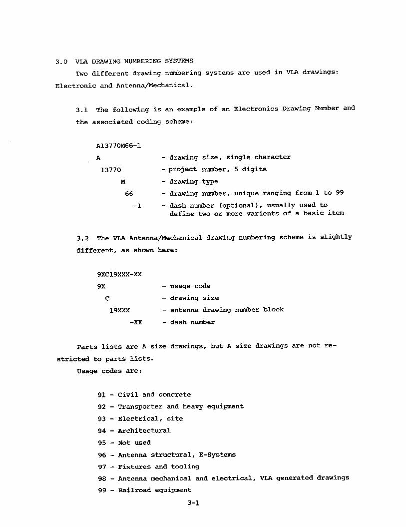
3.0 VLA DRAWING NUMBERING SYSTEMSTwo different drawing numbering systems are used in VLA drawings:
Electronic and Antenna/Mechanical.
3.1 The following is an example of an Electronics Drawing Number and the associated coding scheme:
A13770M66-1A - drawing size, single character13770 - project number, 5 digits
M - drawing type66 - drawing number, unique ranging from 1 to 99-1 - dash number (optional), usually used to
define two or more varients of a basic item
3.2 The VLA Antenna/Mechanical drawing numbering scheme is slightly different, as shown here:
9XC19XXX-XX9X - usage codeC - drawing size19XXX - antenna drawing number block
-XX - dash number
Parts lists are A size drawings, but A size drawings are not restricted to parts lists.
Usage codes are:
91 - Civil and concrete92 - Transporter and heavy equipment93 - Electrical, site94 - Architectural95 - Not used96 - Antenna structural, E-Systems97 - Fixtures and tooling98 - Antenna mechanical and electrical, VLA generated drawings99 - Railroad equipment
3-1

Specifications:
91SXXXXX - site, rail, the equipment telephone cable, communications systems, etc.
98SXXXXX - buildings and other site features E Systems Generation Breakdown, Antenna Drawings - 96E20167 This generation breakdown is very comprehensive and covers the
Electrospace Servo, ACU and NPL equipment.
3-2
4.0 VLA DRAWING TYPESNearly all VLA electronic drawings are one of the following
types:
4.1 Assembly DrawingsType symbol P — These graphically illustrate the physical
orientation, shape and mounting of the components which make up the assembly. Item numbers in balloons link the components to a Bill of Materials which contain the part number, value, reference designator and manufacturers' name. Note references in boxes convey general or specific instructions regarding assembly practices or instructions.
Assembly drawings are used for a wide variety of applications such as modules, PC boards, racks, bins, cables, antennas, subsystems, systems, etc.
4.2 Bill of Materials (BOM)Type symbol Z — The BOM lists all important data about
the assembly drawing items such as part or drawing number, reference designator, value and tolerance, manufacturers' name, quantity required per assembly and so forth.
BOM's should be prepared for each assembly drawing and should reference that drawing and the next higher assembly drawing and BOM, as well as the top assembly drawing and BOM.
4.3 Schematic DiagramsType symbol S — Schematics illustrate circuit design
relationships, signal flow, component reference designators, location designators, values and tolerances, input and output connections, sheet to sheet references and any notes which may be useful for construction, testing or alignment. Phantom lines should enclose portions of a schematic which are contained on more than one subassembly. ANSI and IEEE symbology should be used.
4-1
4.4 Logic DiagramsType symbol L — These drawings illustrate digital logic
design relationships and are functionally similar to schematic diagrams. The logic diagram should show input/output connections, sheet to sheet references, reference designators, location designators, and any notes which may be useful for construction, testing or alignment. Again, phantom lines should enclose portions of circuitry which contain more than one assembly. ANSI and IEEE digital logic symbols should be used.
4.5 Printed Circuit Board MastersType symbol A — These are precision-drawn tape or ink
masters which depict single sided, double sided or multilayer circuit paths. An additional code letter A, B, C, etc. denotes the artwork scale of 1:1, 2:1, 3:1, respectively. Thus, B13720AB17 denotes a 2:1 scale master. Wherever possible, standard pre-cut commercial tape components shall be used in generating a master.The master contains scaling information and alignment targets for photo reduction and fabrication usage.
4.6 Printed Circuit Board Mechanical DrawingsType symbol M — These drawings define the requirements for
drilling, plating, profiling and other mechanical fabrication processes. These drawings are sometime called Drill Drawings.
This type of drawing is distinguished from the Mechanical and Miscellaneous type (also M) by the different nature of the fabrication process so it is treated as a separate type by the Drawing Listing program discussed in Section 9.5.
4.7 Silkscreen MastersType symbol A — Silkscreen masters may be drawn to mark
panels and printed circuit cards.
4-2
4.8 Block DiagramsType symbol B — Block diagrams depict signal flow through
elements rendered as simple blocks whose detailed internal properties may not be vital for the emphasis of the drawing.Signal levels, frequencies, etc. and notes which are useful as maintenance information may be included on the block diagrams.
4.9 Wire ListsType symbol W — Wire lists define wire paths, connections,
wire size, color code, signal names, I/O connections, etc. and are used for rack, module and cable drawings. Special emphasis should be given to the preparation of wire lists so that both the construction and maintenance aspects of wire lists are clearly stated. Mnemonic signal names which are related to circuit function should be used wherever possible.
Wire lists are also generated by computer programs which analyze input data to produce wire lists and wiring machine drive data in several formats.
4.10 Mechanical or Miscellaneous PartsType symbol M — This type encompasses all mechanical piece
parts and miscellaneous items.
4.11 Tool DrawingsType symbol T — This drawing depicts any special tools,
jigs, fixtures, etc. which may be used in building or maintaining VLA electronics.
4.12 Data ListsType symbol D — This drawing contains any relevant physical
or functional data.
4-3


5.0 DRAWING STRUCTUREA set of drawings for an electronic assembly generally has a hier-
archal structure as there are usually two or more levels of subassemblies in a module/rack/subsystem/system. To attain the quality of workmanship we require, it is necessary to control the assembly and wiring of this hardware. Therefore, the drawings should be prepared so that they clearly communicate the required assembly/subassembly relationships.
An important aspect of a hierarchal drawing structure is that it should be possible to trace out the upward and downward relationships of a drawing set by references on the drawings. The "Next Ass'y" and "Used On" references in the title block format provide upward visibility. "Next Ass'y" refers to the next higher assembly level in which the given assembly is referenced as a component part. When used, this scheme nicely links vertically adjacent assembly levels. The "Used On" is conveniently used to span several assembly levels to link a drawing to a major assembly. For example, a Dip Header assembly in the Data Set will cite the Data Set in the "Used On" blank which spans two assembly levels. This feature provides instant association with a major assembly.
A Generation Breakdown drawing provides a broad overview of a major assembly and is structured in a hierarchal manner. E-Systems has prepared a Generation Breakdown for the antenna drawings which provides good visibility for any antenna mechanical or electrical drawing. A Generation Breakdown has been partially developed for the equipment which is installed in the antennas by NRAO.
A drawing tree can also illustrate the hierarchal drawing relationships. Figure 5.1 depicts the Data Set drawing tree.
VLA electronic drawings for an assembly (typically a module) use a Top Assembly drawing and Top Bill of Material as a coupled pair. This pair of drawings is the primary reference for the assembly.The Top Assembly drawing graphically illustrates the physical relationships of the components which are described on the Top Bill of Materials by data such as manufacturers' part number, value, manufacturers' name, etc. The components are cross-referenced by item
5-1

numbers and reference designators. Subassemblies are referenced by item numbers which have the associated subassembly Bill of Materials number as a part number. Each assembly level in a drawing set has a coupled Bill of Materials (BOM) and an assembly drawing which define the components. Figures 5.2 and 5.3 depict the Data Set Top Assembly drawing and Top Bill of Materials.
In special cases other subordinate relationships may exist; for example, a PC artwork master and PC silkscreen drawing are subordinate to the PC drill drawing. These are usually treated as special cases in which the application dictates the approach.
5-2

TOP ASSEMBLY DRAWING - D13720P73 TOP BILL OF MATERIAL - A13720Z99
IC MODULE PANEL
Ass'y Dwg, - C13720P57 Ass'y BOM - A13720Z84
LED DISPLAY SUB ASS fY.
As3'y Dwg. - C13720P38 BOM - A13720Z83 Drill Dwg. - C13720M33 Artwork Dwg. - B13720AB36
A/D CONVERTER SUB ASS fY.
Ass'd Dwg. - D13720P58 BOM - A13720Z85 Drill Dwg. - D13720M45 Artwork Dwg. - D13720AB11
DIP HEADER SUB ASS'YS.
MECHANICALPARTS
Front Panel, Engrvd. - B13720M22 Filter, Red Pol. - B13720M18-1 Filter, Clr - B13720M18-2 Rail Modified - C13720M15-1 Rail Modified - C13720M15-2 Rear Panel - B13450M32 Guide Blocks - B13050M4 Perf Cover - C13050M7 Side Plate - C13720M50 Bracket, Conn. - B1372QM46 Spacer - B13720M47 Side Plate Insul. - B13720M49
I MASTER WIRE LIST
A13720W61
LOGICDIAGRAMSD13720L44
Ass'y Dwg. - Ass'y BOMA13720P62 - A13720Z89 |------ | |A13720P63 - A13720Z90 HAND WIRE MACHINE CONNECTORA13720P60 • A13720Z87 LIST WIRE I/O LIST
LISTA13720P59 - A13720Z86 A13720W62 A13720W63 A13720W64A13720P6 - A13720Z88B13720P16 - A13720Z39B13720P17 - A13720Z9A13720P69 - A13720Z95B13720P14 A13720Z10 FIGURE 5.1 MODEL D DATA SET DOCUMENTATION TREE
IPOKERWIRINGDIAGRAM
D13720L44, SH7

8- \;ct»mn / / » * I f 4 4
t>4>4 H t HHtcirS*A H . T.cnri 0
AJ'kif L* ^ t i *r**i- 4T. *l! iA - M lC B . VAktO
Ncrtr.(T) At-»*.««/« 3#41 1 i t t/a 'm e,*. iK / e t r avd
4(fit!4*CUT, <.0(A1( A f t OX. AS SAOn'M
0 •• it'tf'n'i it frit r toof or suffieifiir true?* rt> 4ito# tit rtQNT rt(*4> hm(u to at iciMf ft At ttAr it rxoirtetb (tt( ri4-i*n)
QJ >41 '**4106 NtfVt 4444133“ (v s f i n Its S i 4 S3 f r fMt 4.0. t#f, t»t?to m > i n it er tovrtt*<?»} /?* tOhrt4 i'4/C (Iff*4 tS) 4*0 Altc r i f t to . m tiHG is to e r xotlreo AtoMi — 7Vf u f f f K £ *h (net* ! * ) ,
S 'iu£tr ,0° "M&ttn (ur« t») 4it ttQ'o, H acfo*/e out f t tmf sc fit * 4iAD amo r*t orurt it r«j f u rue Com (m u if) amp m eA *AK M i ft OTfM 13 ),
0 7*f ’(4 mu Alt OH T4t i f At Of TMt t.tH0JHL4! tvv-ASsr ortM » i 44r to *r
At ftt&P M OM&ft to PHrfMT MrttniAMCf w n rut a-i> ccuntrtA
« a h r ( n o t 4 )
0 Tit 'o x * « b fu c M A T io H s a m w r i t fo g *1*141$ bf/ftjr^mu OHlr AMD A At MOT TO i f 44A 444 p.
0 iCAPS rt4rtl»4TIH<i AT fOS. JO.314 11 USi >rf*f MO. 37
UADi T(f*IIUATlM4 AT fOS. 14 4 IT i / i t l f + t MO. 3 a
M AM t*4*ftHATW4 A7 fOi- 33 4 40
0 iot.pt f 'so to tt nx , O r e *t mo . s o ) t o %vp' WAMt 446 A 4<r vim iter* A14P 4 * * 0 4 . A i v n ( t t r )
m h — — ......... terM-------------f------------ ^ :----------l i l - L j =b=$i------- j —-----' ]H----------y ■ .........— 'ULr+4---------------H --------------- H --------------- H --------------- H v .v .v Ju /eeoooet
Morrsi fcot/r o)io to rn t,no irr»tin4i (i t h a 1 1 ) 10 CKUVHD H4NC (evmroMHT j i e f o f I.C. ffOQt/tC fA u fl ■ H I M ? ) ,
ca 3oi or4 4 * 4 ttahimai ( n r n u \ to“ fW t f t4 U f (W itt- *444 Tt'4M. i t Of OfI.e. MOOl/tr fAMfi. • l/fl me 4 cm avl * 1* 1*4 iM4ti a r
0 » TUT Hf!4C w 4 4 4 1 (4 » . s >4 f 04i.e. Atoemt 4A»ti • / / o f >.
ra Jtr 'fA T Je M T A f f (iT Iti S t ) S 4 A U “ * U N 7 ir rut t 4fMf,74 Ot lllf A A H i
{ I t f M i /f f IT )
0 tCtAfUT I t r 14 t3 to Iff/A 10 HUM O A tou t act r r r r or c f tt rn r A i t msiAu Ai 3*r>#)t in ii t r a-o,
H e e t t i eoHum or nno* ipacch cmooqhTOCUAH WIKE W O A P TtWMiXAt O f Cincvrr e o n n e , r /r t M t o ) .
To ■R °(2)
vyw@ 9 W6
ft ^O 0 o * *ww©© t ^3>(trrj
Uajrfrt'o
0
t * rc ‘c
BILL OF MATERIALS A lS rP O Z ^
FIG AAitroAiAi new or 4#+ «*» M>3
(v n c t 4 S i p t o r /.c mop. s u a - A u r ~ irtm » )
SECT IM S VIEW 0 * 0~ E T ~
OMIiS 0TMtH*.VI ^(CililU OiU(HS*ON> *1*1 IM ifcCHO >«imui tmk.it fti*m«4 M 1 lUkl MCMU > Ui 9 tM lN M I- il 1
N M U U l.
■ HI ,T » » ! . , .
ftmiN:
l | m i
aJ__l^SLt*__OAT A SET MODULE
N A T IO N A L K A D IO A S T R O N O M Y
O B S E R V A T O R Y
♦v L / a
£
Figure 5.2

R E V IS IO N S
REV DATE d r a w n b y a p p r v ’ d b y DE SCRIPTION
- T’ eDkA'-'U FZO/') A J 3 1 l a ^ a Z t C ?V b
/?c-h /iT
) 7 3 0 f / x / / j j c /a jc ^ a/o, 'LS/- 4-3- 3 0 - <? / O
-z>1heJ77 CA*f ££t-t-£t> i t e m 3 d . COZ.££CT£D P/tJ
O F /r£ M S 3 2 . 3 S ~ ? 3 ' 7c
H rCOJ?£FCT£D LEffGTfJS CF /TEMS
q r y o f / r e y j 37 / )a/o p/ / j r o r / o f /re//) 3 3
DRAWN b y d a t e
DESIGNED BY d a t e
D / 3 7 2.0 P 7 3a p p r o v e d BY d a t e
NEXT ASSY USED ON
NATIONAL RADIO ASTRONOMY OBSERVATORY
SOCORRO, NEW MEXICO 67BOIVLA
PR O J EC T
T I T L E
M l ( m o o e l D )
D A T A S E T M O D U L F
°S§ A I 3 7 Z O ? < ) ? SHEET OFFigure 5.3
5-5

BILL OF MATERIALNATIONAL RADIO ASTRONOMY OBSERVATORY \
| | ELECTRICAL [T] MECHANICAL BOM HA13720Z99 REV _C______ DATE ___________ PAGE 1 o f 5 OF
MODULE # M1 NAME DATA SET MODULE DWG # D13720P73 SUB ASMB C IG «
SCHEMATIC DWG II D13720L4*? LOCATION ____________ QUA/SYSTEM ______ PREPARED BY ______________ APPROVED ____
IT\
ITEMfl
REFDESIG
MANUFACTURER MFG PART # DESCRIPTION TOTALQUA
1 N.R.A.O. A13720Z 9? DATA SET MODULE2
3 A13720W 61 WIRE LIST - MASTER4 A13720W 6 Z WIRE LIST - HAND -
5 A13720W 43 WIRE LIST - MACHINE -
6 A13720W.4 4 WIRE LIST - CONNECTOR -
7
8 A13720Z85 A.D. CONVERTER P.C.B. A S S ’Y 1
9 A13720Z84 I.C. MODULE PANEL SUB-ASS'Y 1
10 A13720Z23 L.E.D. DISPLAY SUB-ASS’Y 1
11
12 _ __B13.720M2 2 ENGRAVED FRONT PANEL 1
13 B13450M18 PANEL, .REAR 1
14 ,f C13720M15-1 MODIFICATION, RAIL 1
15 N.R.A.O. C13720M15-2 MODIFICATION, RAIL 1
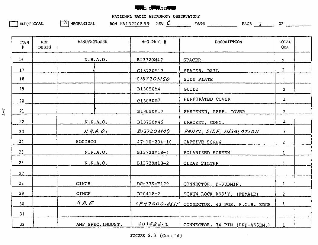
NATIONAL RADIO ASTRONOMY OBSERVATORY1~1 ELECTRICAL Q 3 MECHANICAL BOM ttAl3720Z 99 REV £ ________ DATE ____________ PAGE 2 OF
ITEMii
REFDESIG
MANUFACTURER MFG PART ft DESCRIPTION TOTALQUA
16 N.R,► A.O. B13720M47 SPACER 217 } C13720M17 SPACER. RAIL 218 C 1 3 7 2 0 M 5 0 SIDE PLATE 119 B13050M4 GUIDE 2
20 C13050M7 PERFORATED COVER 1
21 f B13050M17 FASTENER, PERF. COVER 2
22 N.R •o•<• B13720M46 BRACKET. CONN. _ 1
23 A/, # • J Q / 3 7 Z O M 4 9 P 4 h !tL % S / D e , W S t i l A T / O A J /24 SOUTHCO 47-10-204-10 CAPTIVE SCREW 2
25 N.R • A.O. B13720M18-1 POLARIZED SCREEN 1
26 N.R 9 > • o • B13720M18-2 CLEAR FILTER i
27
28 CINCH DC-37S-F179 CONNECTOR. D-SUBMIN. 1
29 CINCH D20418-2 SCREW LOCK ASS'Y. (FEMALE) 230 C P H 7 OO Q»# £ ST CONNECTOR, 4 3 POS. P.C.B. EDGE 1
31
32 AMP SPEC.INDUST. CONNECTOR, 34 PIN (PRE-ASSEM.) 1
FIGURE 5.3 (Cont’d)

BILL OP MATERIAL NATIONAL RADIO ASTRONOMY OBSERVATORY
| | ELECTRICAL QT| MECHANICAL BOM ftAl3720Z 99 REV C________ DATE ____________ PAGE 3 OF
ITEM#
REPDESIG
MANUFACTURER" " — .......MFG PART \\ PESCRIPTION TOTAL
QUA
33 AMP SPEC . INDUST. 202434-4 SHIELD, 34 PIN CONN. 1
34 i
35 6 0 / 4 - $ 8 - 4 CONNECTOR, 42 PIN (PRE-ASSEM.) 1
36 202394-2 SHIELD, 42 PIN CONN. 1
37POS 7 4 - s o%
P I N , CRIMP ( 16 AWG) 3 4 f Z
38 P 7 6 - O O O I - 4 I 4 Z PIN, W V / p o s
39 201143-5 PIN, COAX. 6
40 328666 FERRULE 6
41 201142-2 SPRING, RETENTION 6
42
43 200833-4 GUIDE PIN 2
44 i 202514-1 GUIDE PIN (GND) 2
45 AMP SPEC INDUST. 203964-6 GUIDE SOCKET 4
46
47 H. H. SMITH 2010 TERMINAL (SPLIT LUG) 4
48 H. H. SMITH 2025 TERMINAL (MIN. THROUGH) 4
49

NATIONAL RADIO ASTRONOMY OBSERVATORY| | ELECTRICAL QT] MECHANICAL BOM tf A13720Z9 9 REV C________ . DATE ____________ PAGE _Jj______ OP
ITEM#
REFDESIG
MANUFACTURER MFG PART # DESCRIPTION TOTALQUA
50 6. C. Z L E C T R o k l l C S S 7 0 6 - C LUG, SOLDER 1
51 ALPHA 286 BUS BAR TINNED COPPER (14 AWG) A/R52 BELDEN 8654-50 BRAID CABLE A/R
53 ALPHA P V C -/0 ^ / 6 PLASTIC TUBING (TYPE PVC) J.Q. A/R
54 ALPHA TFT-200/13(NAT .)TEFLON EXTRUDED TUBING A/R
55 >&3THK--MS£LAS==r- -t-
56 CONN. HARD RUBBER CO TYPE K350 KAPTON TEMP-R-TAPE (32/64"WIDE) A/R
57
58 AMATOM 8212-N-440 THREADED STANDOFF (5/16" LG.) 4
59
60 4-40x1/4 LG. SCREW, PAN HD., NYLON 4
61/
4-40x3/8 LG. SCREW, PAN HD., ST. ST'L. 22
62 6-32x.5*/fl LG. SCREW, PAN HD., ST. ST'L. 2
63 6-32x1-1/8 LG. SCREW, PAN HD., ST. ST'L. 2
64 6-32x1/4 LG. SCREW, FLAT HD., ST. ST'L. 6
65 6-32 x 7/m LG. SCREW, FLAT HD., ST. ST'L. 2
66 6-32x % LG. SCREW, SKT. HD. CAP, ST. ST'L. 2
FIGURE .5. 3 (Cont'd)

OT
-'BILL OF MATERIAL
NATIONAL RADIO ASTRONOMY OBSERVATORY ( | ELECTRICAL QT| MECHANICAL BOM tfAl3720Z j£________ DATE ____________ PAGE5 of 5 OF
’Mru i » tei l «
REFDESIG
MANUFACTURER MFG PART (f DESCRIPTION TOTALQUA
57 1
56 ! NO. 6 WASHER, EXT. TOOTH, ST. ST'L. I 0 l.-|oS j NO. 4 WASHER, SPLIT LOCK, ST. ST'L. 22 |
i ...... ..1
11 1
!
i. . . ... .
1 i
11j... ... i
I
J ________ 1
il_____ J' ‘5.3 (Cont’d)

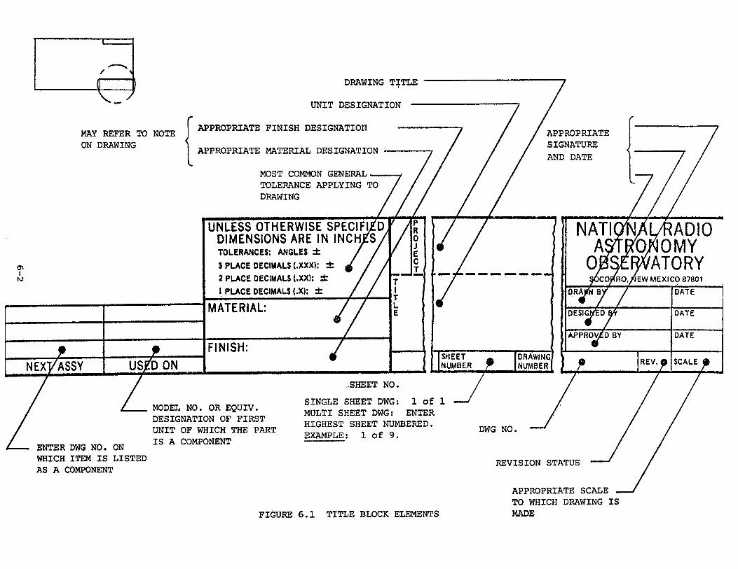
6.0 FORMS AND FORMAT CONVENTIONSFigure 6.1 depicts the VLA Electronic Drawing Title Block Format
and the data entries.Figure 6.2 depicts the Revision Block and entry conventions. The
space below the Revision Block should be left blank so that many revision entries may be made. All sheets of a drawing should be kept at the same revision level as this is more straightforward than a multi-level treatment.
Figure 6.3 depicts the BOM format and the entry conventions.Figure 6.4 is a table of the standard drawing form sizes. These
should be used wherever possible.Always use the smallest form size practical as this makes the
drawings easier to handle on the lab bench. Large drawings may be easier to generate and entail fewer sheets, but are difficult to work with on the bench or in the field.
All sheets of the same drawing should use the same size form.Figure 6.5 is the Change Order form which is a formal change
control form, used principally to control major changes in equipment and drawings.
Figure 6.6 is the cover sheet for A size drawings such as wire lists and BOM's. The entries are identical to the Title Block entries of Figure 6.1b
Figures 6.7 and 6.8 are 16 and 14 pin Dip Header assembly drawing forms. These use the cover sheet of Figure 6.6 for Title Block and revision data.
Figure 6.9 is a general purpose A size form which may be used for applications like BOM notes, Spec Control Drawings, etc.
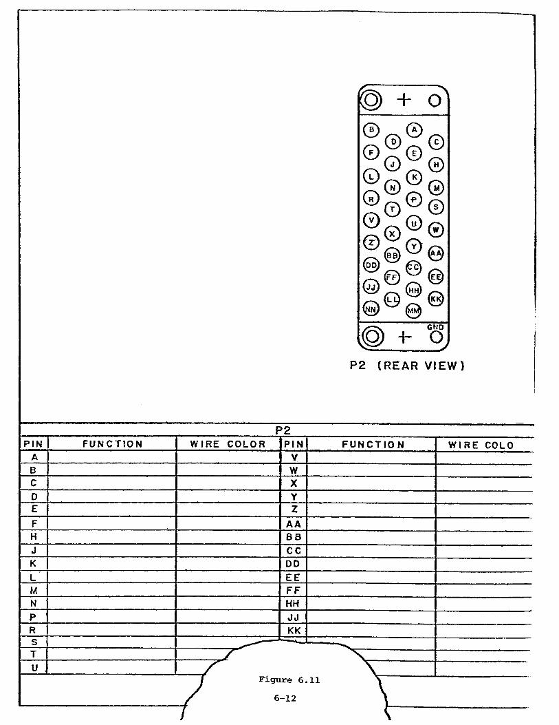
Figure 6.10 through 6.13 are module I/O connector pin/signal lists which define wiring on the module/bin interface connector.
Figure 6.14 is a rack wire list form which defines rack wiring. These forms are particularized to a particular connector and each pin is a nodal point in a to/from format.
6-1
/
MAY REFER TO NOTE ON DRAWING
DRAWING TITLE
UNIT DESIGNATION
APPROPRIATE FINISH DESIGNATION
APPROPRIATE MATERIAL DESIGNATION
MOST COMMON GENERAL TOLERANCE APPLYING TO DRAWING
UNLESS OTHERWISE SPECIFIED DIMENSIONS ARE IN INCHESTOLERANCES: ANQLES ±3 PLACE DECIMALS (.XXX)2 PLACE DECIMALS (.XX): ±1 PLACE DECIMALS (.X); ±
NEXT/ASSY US, D ON
MATERIAL:
FINISH:
APPROPRIATE
D DATE
N A T IQ H A L / f t A D IOa s t j M o m y
O B S E R V A T O R Y50C0^R0f/WEW MEXICO 87801
DR^fW BV / DATE
DESIGNED &Y DATE
( APPROVED BY DATE
REV. O SCALE ®
ENTER DWG NO. ON WHICH ITEM IS LISTED AS A COMPONENT
MODEL NO. OR EQUIV. DESIGNATION OF FIRST UNIT OF WHICH THE PART IS A COMPONENT
-SHEET NO.SINGLE SHEET DWG: 1 of 1 MULTI SHEET DWG: ENTER HIGHEST SHEET NUMBERED. EXAMPLE: 1 of 9. DWG NO,
FIGURE 6.1 TITLE BLOCK ELEMENTS
REVISION STATUS
APPROPRIATE SCALE TO WHICH DRAWING IS MADE

6-3
REVISION LETTER
DATE OF DWG CHANGE
APPROPRIATE SIGNATURE OR INITIALS
SUCCINCT DESCRIPTION OF DWG CHANGE PERTAINING TO EACH REVISION LEVEL.IF REVISION IS THE RESULT OF A CHANGE ORDER, ENTER CHANGE ORDER NO. HERE.
FIGURE 6.2 REVISION BLOCK ELEMENTS
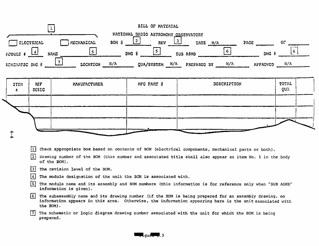
CD BILL DP MATERIAL NATIONAL RADIO ASTRONOMY
| 1 ELECTRICAL
JSODULE H Q
| 1 MECHANICAL
NAME G O
BOM II S REV 3 DATE N/A page or
DWG II 5 SUB ASMB 6 DWG » I 6!
SCHEMATIC DWG II S LOCATION N/A QUA/SYSTEM N/A PREPARED BY N/A APPROVED N/A
PT| Check appropriate box based on contents of BOM (electrical components, mechanical parts or both).[T| Drawing number of the BOM (this number and associated title shall also appear as item No. 1 in the body
of the BOM).f!T] The revision level of the BOM.IT] The module designation of the unit the BOM is associated with.PT| The module name and its assembly and BOM numbers (this information is for reference only when "SUB ASMB"
information is given).Hri The subassembly name and its drawing number (if the BOM is being prepared for an assembly drawing, no
information appears in this area. Otherwise, the information appearing here is the unit associated with the BOM).
|Tl The schematic or logic diagram drawing number associated with the unit for which the BOM is being prepared.

Form Horiz. Vert. Recommended ID ______Dim.________Dim.___________ Usage
A 8*2 11
B 11 17
C 17 22
D 22 34
E 34 44
Cover Sheets for Wire Lists, BOM's Data Lists, etc.
Small, Simple Components
General Use
General Use
Not Recommended for General Use
Figure 6.4 STANDARD VLA DRAWING FORM SIZES

NRAO CHANGE ORDER
78 0( 20 DW W 3 CHANGE ORDER NO. - y - y .zsz
mALS-SEQUENCE NO.
DAT0v_____X— APPROVED BY.
MODULE /RACK TYPE
DATE,
□ DRAWING ONLY
U P D A T E D N U M B E R O F C H A N G E O R D E R S R E Q U E S T E D B Y O R I G I N A T O R D U R I N G C U R R E N T Y E A R
ORIGINATOR'S, W I T \ M _ S
DAY OF M O N T H
attachments: □ p r in t d D sketch □ anotherTsht Q o th e r :
NRAO DRAWINGS .AFFECTED 1 IHOLD FOR VLA APPROVAL FROM SITE [ ] C V APPROVAL O.K.. BY
DRAWING NO. TITLE DRAWING NO. TITLE
FIRST SERIAL NO. AFFECTED: c o p ie s :□ n n n
ROUTING INSTRUCTIONS(CVILLE ONLY) RCVD• BY DRAFTING DATF
DWG CHANGFS BY HATF1--- 1--------------------1__ 1----- ------------
□ oMOD/RACK CHG. BY DATF
I— ICHK. PRINTS SENT TO SITE 1— 1 APPROVAL FROM SITE I— 1 DATE I 1__1 DATE *.
C.O. NO.?
JFIGURE 6.5
6 -6

DRAWN BY DATE
DESIGNED BY DATE
APPROVED BY DATENEXT ASSY USED ON
NATIONAL RADIO ASTRONOMY OBSERVATORY
SOCORRO, NEW MEXICO 8 7 8 0 1
VLA
PROJECT
T I T L E
— - — ■ ■ ' — ■ ■c ~
DWGNO. SHEET OF
Figure 6.6
6-7
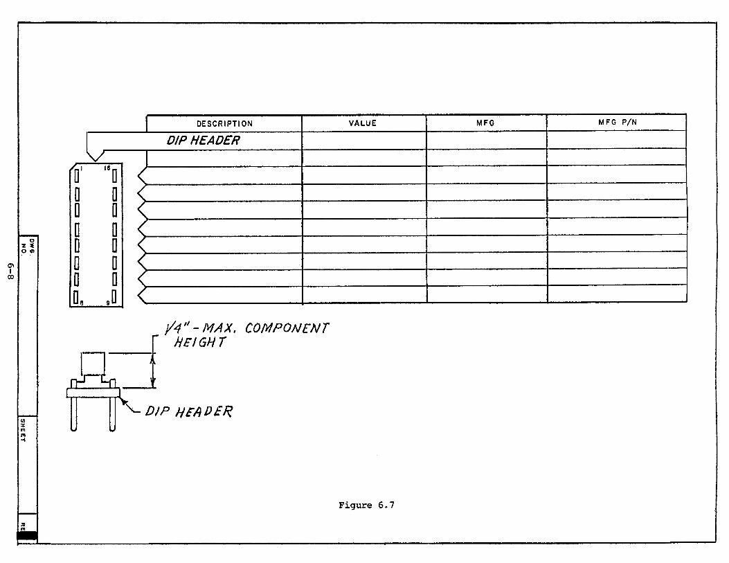
o z tO 6>
DESCRIPTION VALUE MFq M FG P/N
DIP HEADERV
0 10 0 <
0 0 <
0 0 ?Q 0 ?
0 n <
0 0 <
0, ,0 <
f a " -M A X . COMPONENT HEIGHT
DIP H£AD£R
Figure 6.7
m__

o z * o o
DESCRIPTION VALUE MFG MFG P/N
DIP HEADER
0 0
0 D Q Q
D 0 0 D D 0
Dr ,D
1/ 4 "- MAX. COMPONENT H E I G H T
[r T r P - r i1_
D IP h e a d e r
F ig u r e 6 .8

Figure 6.9
6-10

-ruS IN G LE W IDE M ODULE
( REAR V I E W )
4- O
0 ^ © ^ © © ©
© ~ © ~ ©
© „ © , - . © 2
© @ ©
© s ©© s ©
© @ © ~ @ x © © ©© © ©
GND
+ o.PI ( R E A R V I E W )
PIPIN FUNCTION WIRE COLOR PIN FU N CTIO N WIRE COLOR
1 2 22 233 244 255 2 66 277 2 8 - 2 8 VDC GREEN8 29 + 2 8 VDC GREY9 3010 + 5 VDC ORANGE 3111 - 5 V D C BROWN 3212 3313 34 PWR. GROUND BLACK14 3515 3 616 +- 15 VDC RED 3717 - I 5 V D C YELLOW 3818 3919 --------------- x2 021 Y l . GROUND* IN D IC A T E S A FUNCTION NOT FOUNI F i g u r e 6 . 1 0
6-11
P 2 ( R E A R V I E W )
P2PIN FUNCTION WIRE COLOR PIN F U N C T IO N WIRE COLO
A VB WC XD YE ZF AAH BBJ CCK DOL EEM FFN HHP JJR KKS r__—TU .
Figure 6.11 6-12

_nJS IN G L E WIDE MODUL E
( REAR V I E W )
© r . © ^ © © ©
© ^ © ^ ®
© ~ © „ ® © ©2
©®0®r©
© s ©© ©
©^©X© © ©© © ©
GND
+ - O
PI ( R E A R V I E W )
6-13
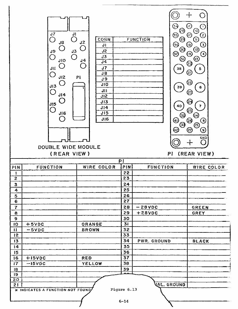
CONN FUNCTIONJlJ2J3J4J7J 8J 9JIOJilJI2J I3J I4J 15JI6
DOUBLE WIDE M O D U LE ( R E A R V IEW )
+ o© ~ ©
0 ©© © ©
(39 (12) © ^ ® ^ ©
31} (13
© S O
©2©©2©
© 0 © ~ @ „ ©
© ®
GND
+ o
PI (REAR V I E W )PI
PIN FUNCTION WIRE COLOR PIN FU N CTIO N WIRE COLOR222 32 42526272 8 - 2 8 VDC GREEN
8 29 + 2 8 VDC GREY30
10 + 5VDC ORANGE 31II — 5VDC BROWN 3212 3313 34 PWR. GROUND BLACK14 3515 3 616 + I5VDC RED 3717 — 15 VDC YELLOW 381819
39
2021 AL. GROUND* IN D IC ATE S A FUN CTIO N NOT FOUND,
6-14


7.0 DRAWING PROCEDURESThis section sets forth drafting procedural guidelines.
7.1 Drawing ControlAt present, VLA electronics design control authority operates
at two levels:
System Level — At the System Level the Systems Engineer defines system performance requirements, interface specifications and system configuration. The Systems Engineer may direct design/drawing changes by means of a Change Order or Revision Request. This would usually be done in consultation with the engineer responsible for the particular subsystem.
Responsible Engineer Level - The engineer responsible for a system/subsystem may direct drawing revisions which do not conflict with the VLA System specifications. Design changes which might impact these specifications must be approved by the Systems Engineer. Within these constraints the Responsible Engineer (or his delegate) may issue any Revision Requests or generate any required drawings to implement designs, correct errors and improve performance, reliability or manufacturability.
Drawing changes are not permitted outside the authorization areas cited above.
At some future date drawing revision authority may be changed to a more formal approval procedure than that cited above.
7.2 Change Orders and ProceduresMajor changes in the VLA system configuration, rack wiring,
module design, component selection and drawings are directed
7-1

by a Change Order. The form and entry conventions are shown in Figure 6.5. Change Orders are used for all changes directed to Charlottesville by the VLA site engineers and for major changes at the VLA site by site personnel.
Entries on the form provide an orderly check list for distribution, drawing and hardware changes and serial numbers affected by the Change Order.
Change Orders are generated by engineers and technicians and are reviewed by the Systems Engineer.
When a Change Order is generated a copy of the Change Order and associated data should be sent to the VLA site drafting files.
7.3 Drawing RevisionsIt often becomes necessary to change drawings to correct
errors and improve performance, manufacturability or maintainability. This process is called drawing revision and is initiated by a Revision Request or Change Order.
The Revision Request should cite the affected drawings and include a written statement of the required changes. A red-lined (annotated) print may serve as an alternate to the written directions. The Revision Request is placed in a pending revision file in drafting and will be implemented in the queue order if the change is not urgent.
The Responsible Engineer (or a delegate) should carefully review and approve the revised drawings.
The revision blocks on the drawing should be updated to show the new revision level, date, a succinct description of the change (including Change Order number, if appropriate) and approval initials by the Responsible Engineer (or his delegate).
Revisions need not be made for a very small change (such as a screw detail, etc.) but should be made for major performance/ configuration changes or when a number of small changes have
7-2

accumulated. If a unit is to be built by a contractor all drawing errors should be corrected prior to the issuance of an RFQ.
Avoid the protracted use of red-marked prints, as change details are easily lost or forgotten and red-marked prints quickly become dog-eared or misplaced.
If drawing revisions are extensive or there is the possibility of configuration confusion then another set of reproducible drawings may be required to record the pre-revision configuration, even though the older configuration may be in a transient state. This requirement for separate reproducibles may be necessary because of the time required to implement the changes and the number of units which may still be in service. All units in service must be backed up by a reproducible set of drawings- When upgrading modifications are completed the older or transient drawings should be marked "obsolete" and dated and signed by the Responsible Engineer. The obsolete drawings should be kept in a dead file for a while.
A complete set of reproducible drawings shall be retained in the drawing files in cases where a unit is built to early drawings and is retained in service in its unmodified state.
When a unit is retired from service and will no longer be used (even in emergencies), then the associated reproducible drawings should be marked "obsolete" and dated and signed by the Responsible Engineer. The obsolete drawings should be retained in a dead file for a while.
If revisions are very extensive the "Model" documentation scheme discussed below should be considered.
7.4 New DesignsIn the course of executing a new design the engineer should
formulate a drawing plan which outlines the types and quantities
7-3
of drawings to be prepared. The engineer will generally have a packaging concept which will produce the best performance; this should be the basis for the package design. The engineer should work out the drawing structure with the draftsmen who will make suggestions as to the most appropriate means of incorporating the construction requirements in the drawings.
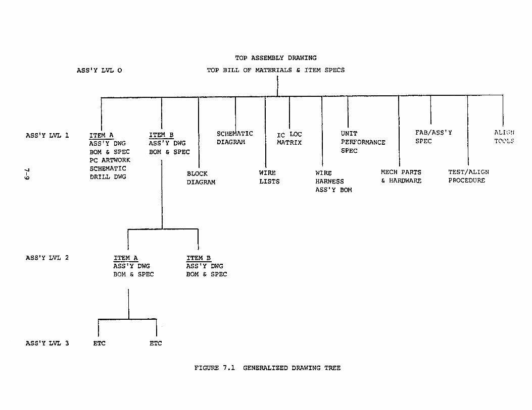
Figure 7.1 is a generalized documentation tree which is recommended for all VLA electronics modules and major assembly documentation. The composition of drawing types must of course be tailored to the application, but by the use of this structure one can be sure that the documentation for a unit is complete, coherent and completely defines the construction requirements.
A Top Assembly and Top BOM drawing should always be generated, no matter how simple the assembly. All the dominant configuration features are derived from this pair of drawings; typical items are I/O connector numbers, subassembly names, wire harness routing, semi-rigid coax routing, maintenance access and test points, assembly procedures and constraints, etc.
Where there are important process or assembly requirements, such as the assembly procedure for OMQ connectors, the appropriate specification should be cited in the assembly drawing notes.
Circuit schematics, logic diagrams, wire lists and assembly drawings should be prepared so that the unit's operating principles are easily understood from the drawings. Maintenance information such as signal levels and tolerances, critical and alignment adjustments, troubleshooting notes, signal waveforms, etc. should be included on the schematics and block diagrams wherever possible.
Each module and system in the VLA has (or will have) a Manual which serves as a maintenance manual and design description. The manual will typically contain a theory of operation, performance and interface specifications; diagnostic and trouble-shooting
7-4
information, schematic and logic diagrams, parts lists, data sheets for special purpose components, and a documentation tree (or drawing list). These manuals should be updated to reflect revisions or model changes and should state explicitly to which models they apply.
It is desirable to add the manual number and title to the associated documentation tree.
7.5 Model DocumentationWhen there exists more than one hardware type of a unit with
significant differences between them use "Model" documentation in which there exists a set of reproducible drawings for each model. This practice can simplify the drawings for the two (or more) units by eliminating the need for complex and extensive configuration notes on one set of drawings. The second set of reproducible drawings can be generated quite easily by making a mylar sepia copy of one configuration. The copy then may be particularized for one model and the original set may be particularized for the other model. With care, an almost unlimited set of reproducible drawings may be generated which are never more than one generation from the original. Only a few hours are required to generate and detail a set of model drawings.
Drawings for items which are common to the two (or more) models should not be duplicated, but it may be desirable to update the "Used On" and "Next Assembly" blocks in the Title Block.It is generally desirable to generate a documentation tree for each model if there is a possibility of configuration confusion.
The criteria for the use of Model documentation are highly judgemental, but, in general, if there is more than one implementation of a unit with differences in design, operating characteristics, signal levels, I/O connections, components or physical configuration, then the Model approach should be used.
7-5
In using this approach one should assign new drawing numbers to the "new" model drawings or indicate model level in the Title Block. Revisions and changes can be made to each model set independent of the other model drawings.
When a new model is generated (either by modification or new construction) the module serial numbers should be altered to reflect the change. Specification A13010N1A, Section C states:
"Each module will have a 2 or 3 character serial number such as A1 or B13. The first character notes a particular version or revision; the second character is a consecutive serial number not affected by the revision letter (i.e., if 2 version A modules, A1 and A2, were built the first revision B module would be labeled B3).The serial number shall be marked with 1/8" letters on the lower front panel."
In conformance to this specification a new model (i.e., version) would incorporate the next alphabetic letter in the serial number.
Examples of model documentation are the Models C and D Data Sets which are logically identical but have significant differences in hardware components and internal wiring.
7.6 Drawing ChecksThe site VLA Electronic Drafting Group does not usually
provide a drawing checker service. This task is currently the responsibility of the Responsible Engineer but some assistance may be provided by drafting if requested and if the workload permits.
7.7 VLA/CV Drafting LiaisonThe VLA site and Charlottesville draftsmen are responsible
for liaison between the two drafting groups to coordinate
7-6

drawing number usage, revisions, the interchange of check prints and replenishment of the VLA print library. When additional copies of prints or some drafting-related service is required, the draftsmen at either facility should be contacted.
The draftsmen are also responsible for coordination, drawing revisions and the acquisition and distribution of check prints associated with Change Orders or Charlottesville-generated drawings.
7.8 VLA Print LibraryA complete set of copies of Charlottesville-generated VLA
drawings is maintained by drafting in a print library. When new drawings are generated in Charlottesville, they are added to the library files. When drawings are revised by Charlottesville drafting, copies are placed in the library files. Prints are available on request for any drawings which are stored in the site drawing files.
7.9 Drawing Number AssignmentsDrawing numbers are assigned by the VLA draftsmen and re
corded in a log book by title, number, size and drawing originator. The Charlottesville and VLA draftsmen coordinate the number assignments but do not maintain duplicate logbooks. The engineer should supply the project number associated with the unit to be drawn as it is incorporated in the drawing number.
7.10 VLA Drawing Number/Title ListsComputer-generated drawing listings are available which list
all VLA electronics drawings on the basis of module association. This listing can quickly answer a question like "What are the drawings for the Data Set?"
The computer data files containing this information are periodically updated. This program and the data files currently
7-7

reside in the Charlottesville 360, but it is planned to implement this listing capability in the DEC-10 System. The data formats for entry into the data files are depicted in section 9.5 of this manual.
7.11 Drawing PriorityThe priority levels normally used by the VLA site electronic
drafting group are as follows:
1. Drawings and revisions necessary for construction or impending contractual use.
2. Revisions, drawings of various sorts which are not required for imminent construction.
3. Manual illustrations, etc.
7-8
ASS'Y LVL OTOP ASSEMBLY DRAWING
TOP BILL OF MATERIALS & ITEM SPECS
ASS'Y LVL 1 ITEM A ASS'Y DWG BOM & SPEC PC ARTWORK SCHEMATIC DRILL DWG
ITEM B ASS'Y DWG BOM & SPEC
SCHEMATICDIAGRAM
IC LOC MATRIX
UNITPERFORMANCESPEC
FAB/ASS'Y SPEC
BLOCKDIAGRAM
WIRELISTS
WIRE HARNESS ASS'Y BOM
MECH PARTS & HARDWARE
TEST/ALIGNPROCEDURE
ITEM B ASS'Y DWG BOM & SPEC
ASS'Y LVL 3 ETC ETC
ASS'Y LVL 2 ITEM AASS'Y DWG BOM & SPEC
ALIGNTOOLS
FIGURE 7.1 GENERALIZED DRAWING TREE


8.0 DRAFTING CONVENTIONS
8.1 General Requirements
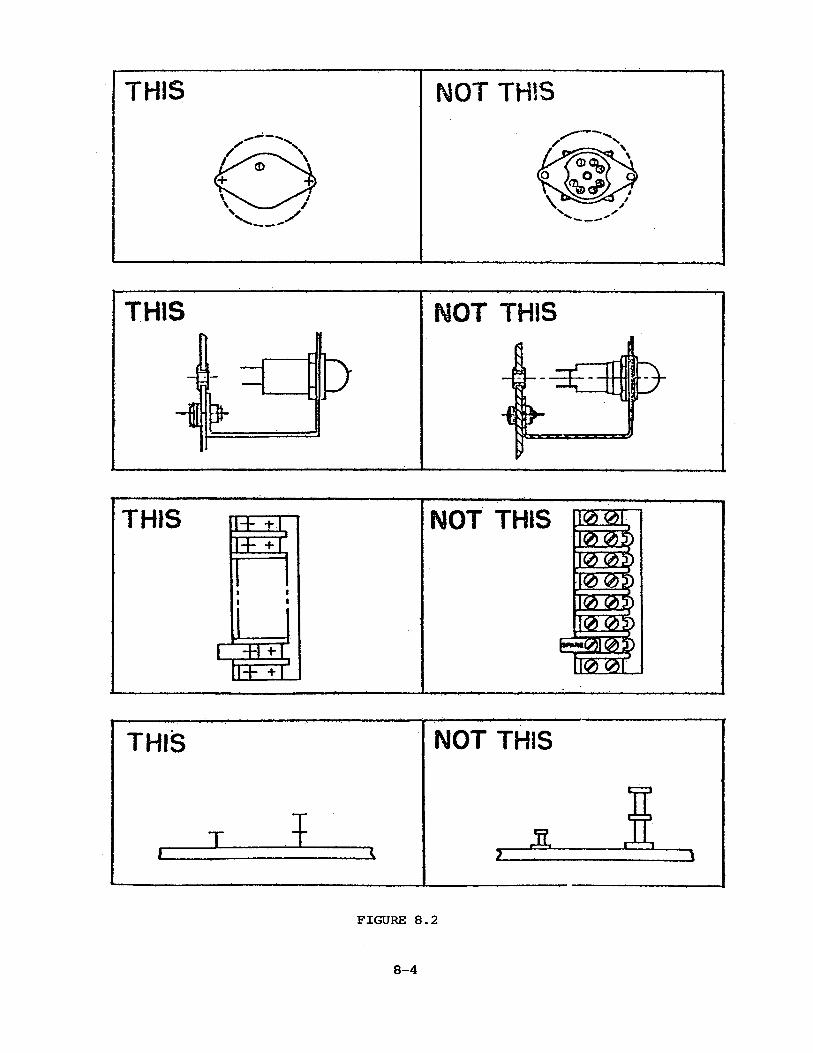
8.1.1 A drawing shall contain only the minimum of delineation, but with sufficient technical information so that the items may be fabricated and inspected. Drawings may be preparedby the use of instruments, or freehand (unless specified otherwise). Use of aids such as a grid underlay and templates are encouraged.
8.1.2 Simplified drafting [the elimination of extra views, unnecessary elaboration (e.g., shading), superfluous lines and repetitive information] shall be used to reduce the time and effort in producing the drawings. Figures 8.1 and 8.2 illustrate this principle.
8.1.3 Reproducibility and legibility - Drawings, including those made freehand, shall be legible and shall be reproducible to at least a second generation reproducible drawing capable of being reduced.
8.1.4 Views vs. shape by description - Avoid views when the shape can be given by description (e.g., HEX, SQ, DIA,THK). Show only partial views of symmetrical objects.
8.1.5 Repetitive detail - Avoid the use of elaborateor repetitive detail and avoid repetitive data by use of general notes. Encode identical items on assembly drawings wherever possible.
8.1.6 Hardware details - Omit nonessential details of nuts, bolt heads, and other hardware. Show plain outlines when it is necessary to indicate/position. Knurling shall not be shown.
8 -1

8.1.7 Detail of parts on assembly drawings - Omit details of parts on assembly drawings, except when such details are necessary to show the location and orientation of the item.Do not show chamfers or corner radii when these featuresare not necessary for interpretation of the assembly drawing.
8.1.8 Hidden lines - Avoid the use of hidden lines which do not add clarification. Do not dimension to hidden lines.
8.1.9 Cross-sectioning - Use partial cross-sectioning only, and then only when the clarity of the drawing depends upon it.
8.1.10 Shading shall not be used.
8.1.11 Drafting aids - Make maximum use of available templates and decals.
8.1.12 Simplified drafting illustrations - The illustrations in figures 8 .1 and 8.2 offer some practical suggestions on the application of the above principles.
8.1.13 Views, projections and sections - Views, projections and sections on drawings shall comply with good drafting practices utilizing third angle projection. If other forms of illustrations are utilized (e.g., isometrics), they must be complete to the degree necessary for proper delineation of the intended item.
8.1.14 Scale - With the exception of freehand applications, drawings should show an object or assembly to full scale.When full size is not practicable, drawings may be prepared to reduced or enlarged scale. Should views and/or sections be of a scale other than that given for the drawing, the appropriate scale shall be indicated.
8-2
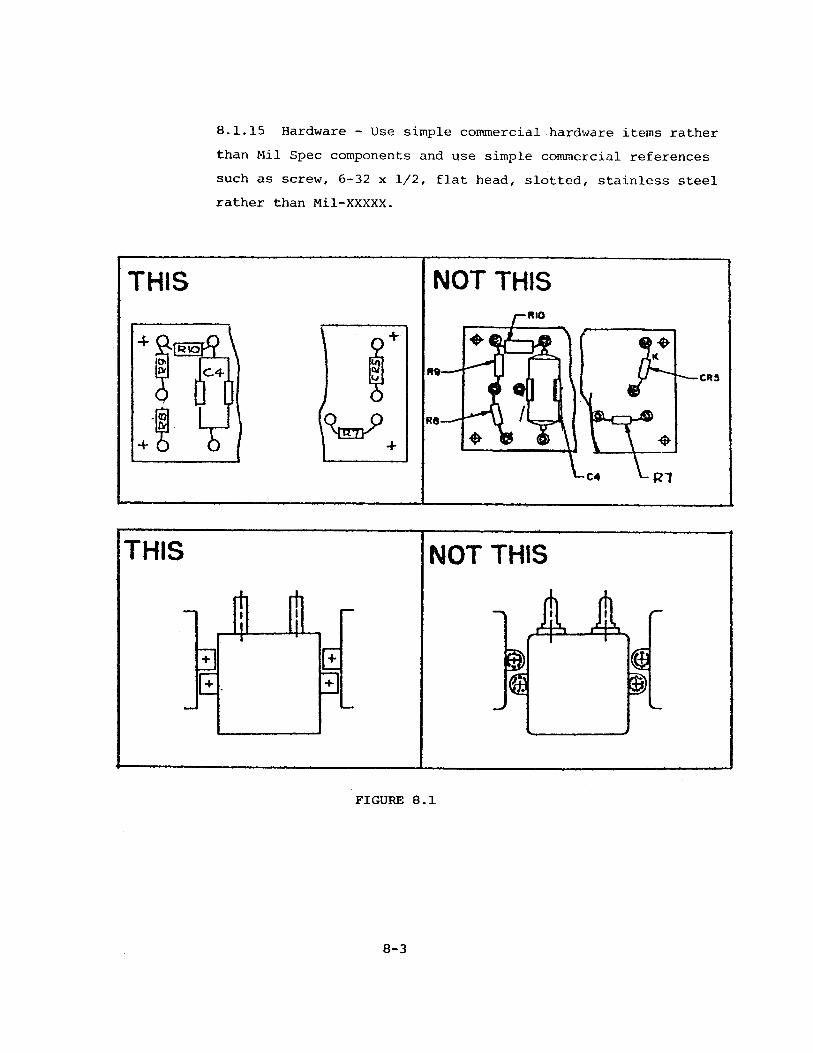
8.1.15 Hardware - Use simple commercial hardware items rather than Mil Spec components and use simple commercial references such as screw, 6-32 x 1/2, flat head, slotted, stainless steel rather than Mil-XXXXX.
FIGURE 8.1
8-3
T H I S
t ;l---------- *■" ■ ..... ■ .............. 'i
N O T T H I S
cpp
c~p
7----- ^ -------------- 1-----1-------»I... ............. ............. \ 2------ --------------------------- - j
FIGURE 8.2
8-4

8.1.16 Titles, drawing - Keep drawing titles as brief as possible- Use upper case letters. No title search is required. Make the main part of the title a noun or brief noun phrase describing the item. Use similar titles on assemblies and their associated documents.
8.2 flotes on Drawings
8.2.1 Local notes are located in the field of a drawing adjacent to the point of application and usually apply only to a specific feature of the item described on the drawing.
8.2.2 General notes are grouped together and placed in a convenient location, preferably on the left-hand side of the drawing. General notes apply to the entire drawing (e.g., protective finish, heat treatment or to a specific feature which appears in several locations).
8.2.3 A note number, when enclosed by a box, in the general notes indicates a reference in the field of the drawing. See figure below:
N O T E S i. A S S E M B L E PER XXXXXX
[2]M A R K
EXAMPLE OF NOTE NUMBER REFERENCE
8-5
8.2.4 On multi-sheet drawings, place the general notes on sheet 1.
8.2.5 Material designation - The material designation should be specified either in the Title Block (preferred) or in the general notes. When material is specified inthe general notes, it must be preceded by the word "material" (e.g., MAT'L, ALUM, 6061-T6). Reference the note number in the Material Block.
8.2.6 The note "Reference" denotes a redundant item callout on an assembly drawing and is generally associated with additional views which illustrate some aspect of the assembly.
8.3 MarkingIf item identification and/or general marking is required,
the marking shall be as follows:
8.3.1 Location - Do not dimension the location of the marking unless the location is critical.
8.3.2 Method of applicationa. When no specific marking process is required, a general note may be specified on the drawing.
Example: MARKING SHALL BE — HIGH, LEGIBLE AND PERMANENT. LOCATE APPROX WHERE SHOWN
b. When a specific marking process is required, the process will be specified in the general notes.
Examples: ENGRAVE __________ HIGH __________HOT DIE STAMP __________ HIGH BLACK _______
8.3.3 Size - Specify the size of marking such that its minimum size will be legible.
8.3.4 Item identification marking - To be delineated at the appropriate drawing level.
8-6

a. Assemblies and details. Required marking may be shown, per figure below, with a reference to the general notes, which call out the marking required.
Notes:
m Mark part number. Indicate the number or name you want marked.
8.4 Revisions of Drawings and Lists
8.4.1 No controlled drawing or list may be altered in any manner without authorization via an approved Change Order or the direction of the responsible engineer.
8.4.2 When practical, make changes to scale.
8.4.3 Delete a view, detail, section, local or general note, or entry on a manually prepared list by erasure or lining out (preferred unless confusing).
8.4.4 Record each revision or authorization in the revision block, including date and initials of participants.
REV. DATE DRAWN BY A P PR V D BY DESCRIPTION
A \ DELETED ITEM S T j 9 ZONE c - a
B %M L RESISTOR VALUES CHANGED FRO M IK-ft. TO 100 KS2. PER C.O. NO.-------
EXAMPLE OF REVISION BLOCK ENTRIES 8-7
8.4.5 When a drawing or list is revised or redrawn, identify the revision by the revision letter next in sequence.
8.4.6 A redrawn document need not include the previous revision record, deleted views or notes.
8.4.7 Inactivation of drawings and lists - No controlled drawing or list shall be inactivated unless such actionis authorized by the responsible engineer or a Change Order.
8.5 Dimensioning and Tolerancing
8.5.1 Fundamental rules for dimensioning - Dimension and tolerance parts to ensure interchangeability. Show only enough dimensions so that sizes, shapes, and locations can be determined without calculating or assuming any distances.ANSI Y14.5-1973 shall be the standard for dimensional practices.
8.5.2 The decimal system of dimensioning is preferred.The fractional system is optional.
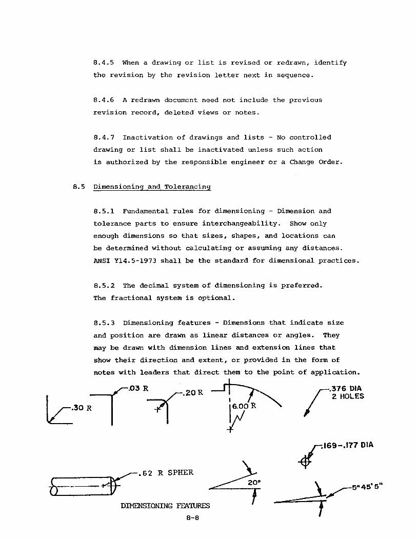
8.5.3 Dimensioning features - Dimensions that indicate size and position are drawn as linear distances or angles. They may be drawn with dimension lines and extension lines that show their direction and extent, or provided in the form of notes with leaders that direct them to the point of application.
I69-.I77 DIA
DIMENSIONING FEATURES
62 R SPHER
8-8
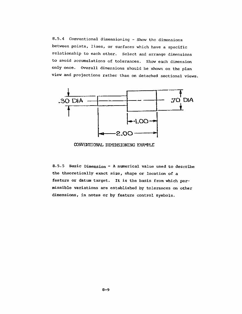
8.5.4 Conventional dimensioning — Show the dimensions between points, lines, or surfaces which have a specific relationship to each other. Select and arrange dimensions to avoid accumulations of tolerances. Show each dimension only once. Overall dimensions should be shown on the plan view and projections rather than on detached sectional views,
i.30 DIAT
•1 . 0 0
««---- 2 . 0 0
h f.70 DIA
CONVENTIONAL DIMENSIONING EXAMPLE
8.5.5 Basic Dimension ~ A numerical value used to describe the theoretically exact size, shape or location of a feature or datum target. It is the basis from which permissible variations are established by tolerances on other dimensions, in notes or by feature control symbols.
8-9
a. EXAMPLE OF ORDINATE DIMENSIONING FROM A CUT EDGE
b. EXAMPLE OF ORDINATE DIMENSIONING FROM A FORMED EDGE1.50
c. EXAMPLE OF ORDINATE DIMENSIONING FROM A FEATUREFIGURE 8.3
8-10
8.5.6 Ordinate (arrowless) dimensioning - Establish two mutually perpendicular datum lines for each view. Normally, a cut edge or a formed edge should be used. See Figure8.3 a and b above. When tolerances for fabrication of a part are greater than those for the location of features within the part, the first row of features may be used to establish a datum line, as shown in Figure 8.3 c. In such cases, the overall fabrication dimension shall be conventional. Identify the datums as zero.
8.5.7 All ordinate dimensions are shown with respect to the datum lines. Locate the dimension at the ends of extension lines, preferably in a single line, as shown in Figure 8.3 above.
8.5.8 Do not place conventional dimensions in line with ordinate dimensions.
8.5.9 Show only 1 datum per axis.
8.5.10 Ordinate (arrowless) dimensioned drawings may also employ conventional dimensions between related features or to locate datum lines not established by formed or cut edges.
8.5.11 Tabular dimensioning - When a large number of similarly shaped features must be located, use tabular dimensioning.
Identify each feature which is to be tabulated with a letter and numeric suffix, omitting I# O, Q, and X. For identical features, use the same letter with sequential numerals (e.g., Al, A2, A3). Make a table listing each feature, its position, and size as shown in Figure 8.4.
Establish two mutually perpendicular datum lines, using formed or cut edges, or a hole location. Indicate the
8-11
2.00 2 .00 -
HOLE POSITIONHOLE S IZE
ID EN T X - * - Y tAt ,o o ,ooAX 2.62 3.62. .067- ,070 01A
A3 .00 3.2-£~
Bt .30 3.10 >093-096 Of A
El XSO 2 .0 0VIEW Ee x 5~.QO 2 .0 0
VIEW E
0 &7 -.0 7 0 0 /1 x H O L E S
FULL R> 2 . p l a c e s
FIGURE 8.4 EXAMPLE OF TABULAR DIMENSIONING
8-12
direction of X and Y coordinates as shown in Figure 8.4. Relate all tabular dimensions with respect to these datums.
All dimensions of form for the part containing the features tabulated shall be conventional dimensions.
8.5.12 Tabulated detail drawing - Generate when required to depict two or more parts which have the same basic shape, but vary in size, finish or other characteristies.
Pa * T N O ; A BX X X X X X - I £ . 0 0
oo
o
c
o o
- 2 .JuSfi.,
EXAMPLE OF TABULATED DETAIL8.5.13 Monodetail drawing - Depict complete end item requirements for a single part.
EXAMPLE OF MONODETAIL 8-13
8.6 Electrical Component Parts
8.6.1 Wherever possible minimize the necessity for reference to other drawings for simple information like component values, reference designators, etc. by incorporating this information on schematic diagrams.
8.6.2 Use "typical" value notations to minimize repetitious detail on drawings. For example, if the same value of limiting resistor is used for a group of LED's then the value should be entered once with the adjacent note "Typical."
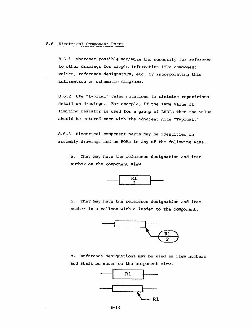
8.6.3 Electrical component parts may be identified on assembly drawings and on BOMs in any of the following ways.
a. They may have the reference designation and item number on the component view.
R1
b. They may have the reference designation and item number in a balloon with a leader to the component.
c. Reference designations may be used as item numbers and shall be shown on the component view.
---- R1 -----
d. Reference designations may be shown on the component view as (c) and included in the description column of the BOM.
8.6.4 When nominal value components are to be selected at unit or system test, the component shall be identified on the assembly view with either "NU" or "NS" as applicable, and the range of values may be listed in the BOM or on a separate document which is listed in the BOM. See also paragraph 8.7.7.7.
8.7 Schematic and Logic Diagrams and Interconnections
8.7.1 Title - Title the diagrams the same as the corresponding assemblies plus "SCHEMATIC DIAGRAM" OR "INTERCONNECTION DIAGRAM,” e.g., "POWER SUPPLY SCHEMATIC DIAGRAM."
8.7.2 Symbols - Use IEEE and ANSI standard electronic symbols.
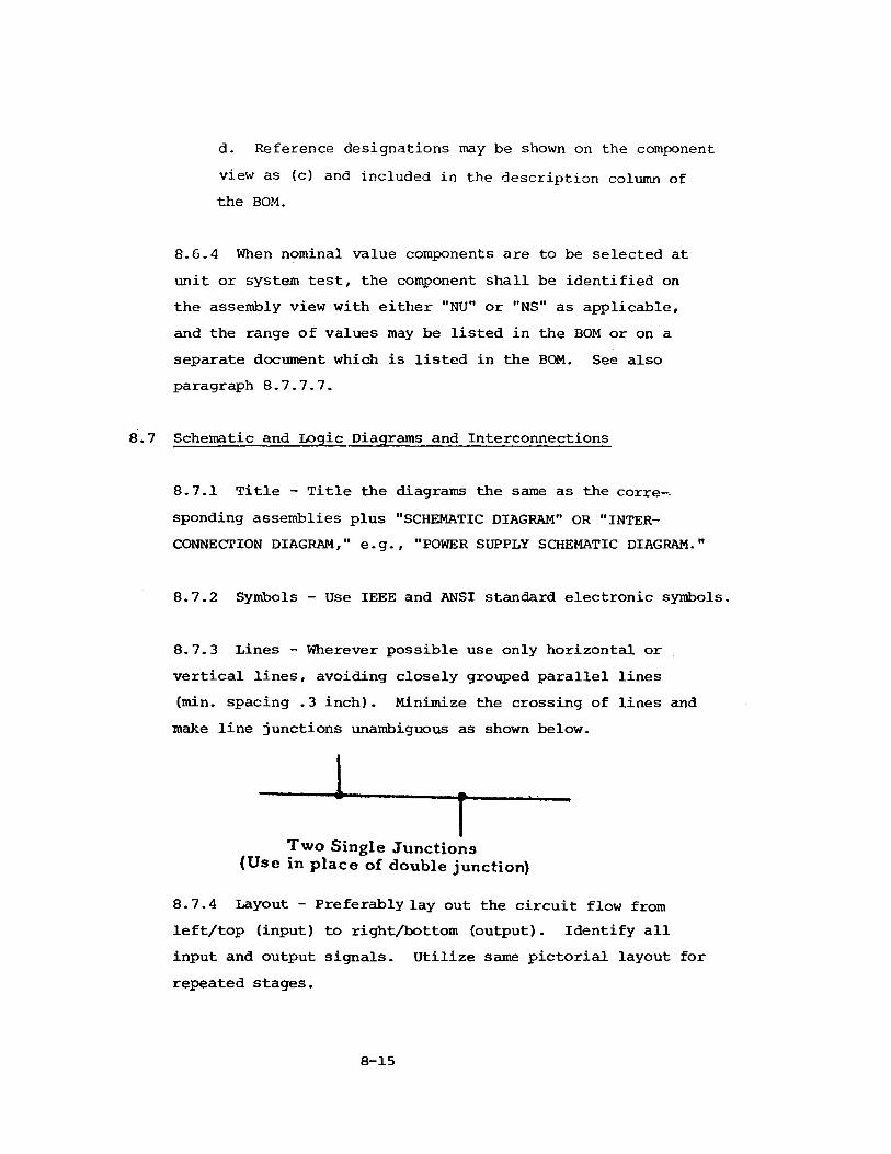
8.7.3 Lines - Wherever possible use only horizontal or vertical lines, avoiding closely grouped parallel lines (min. spacing .3 inch). Minimize the crossing of lines and make line junctions unambiguous as shown below.
-------- *■» »
Two Single Junctions (U se in p la ce of double junction)8.7.4 Layout - Preferably lay out the circuit flow from left/top (input) to right/bottom (output). Identify all input and output signals. Utilize same pictorial layout for repeated stages.
8-15
8.7.5 Multisheet - Identically identify corresponding lines between sheets.
Arrange logically related circuit functions on the same sheet to minimize the number of sheet-to-sheet references. This can be quite burdensome to a drawing user. Do not use arrows on these references.
+2 50VDC—100VDC
SYS GRD
LEVEL ADJ
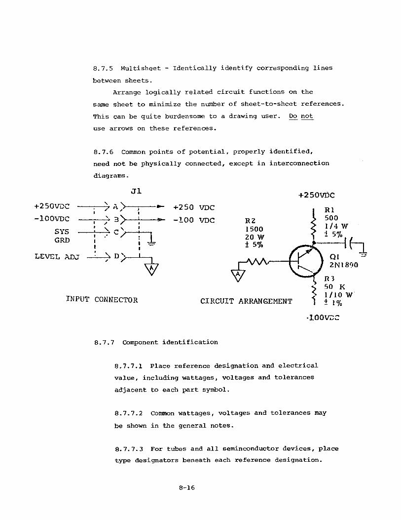
8.7.6 Common points of potential, properly identified, need not be physically connected, except in interconnection diagrams.
a 1------- .------,
✓1
\
1 ✓11 \
111
*
1\
— *
c >1
INPUT CONNECTOR
+250 VDC - 1 0 0 T O C R 2
1500 20 W ± 5%
+250VDC
CIRCUIT ARRANGEMENT•lOOVDC
8.7.7 Component identification
8.7.7.1 Place reference designation and electrical value, including wattages, voltages and tolerances adjacent to each part symbol.
8.7.7.2 Common wattages, voltages and tolerances may be shown in the general notes.
8.7.7.3 For tubes and all seminconductor devices, place type designators beneath each reference designation.
8-16
8.7.7.4 Components with unmarked terminals require a physical diagram on the schematic, showing terminal orientation and assigned designations.
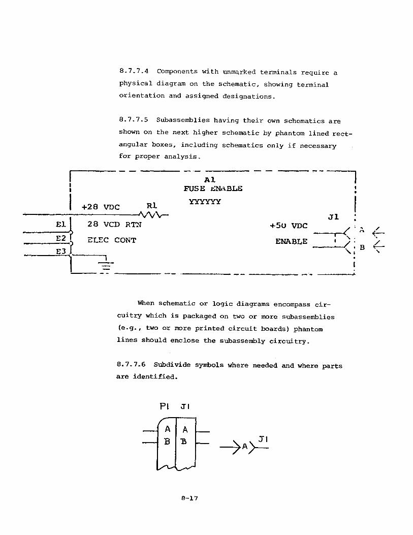
8.7.7.5 Subassemblies having their own schematics are shown on the next higher schematic by phantom lined rectangular boxes, including schematics only if necessary for proper analysis.
AlFUSE JfclNABLS {
o1 YYYYYY+28 VDC RJ---------- -----A y V V — ji28 VCD RTN +5U VDC ^ \ ELEC CONT ENABLE ‘ ^ ■
\ ! i
i
When schematic or logic diagrams encompass circuitry which is packaged on two or more subassemblies (e.g., two or more printed circuit boards) phantom lines should enclose the subassembly circuitry.
8.7.7.6 Subdivide symbols where needed and where parts are identified.
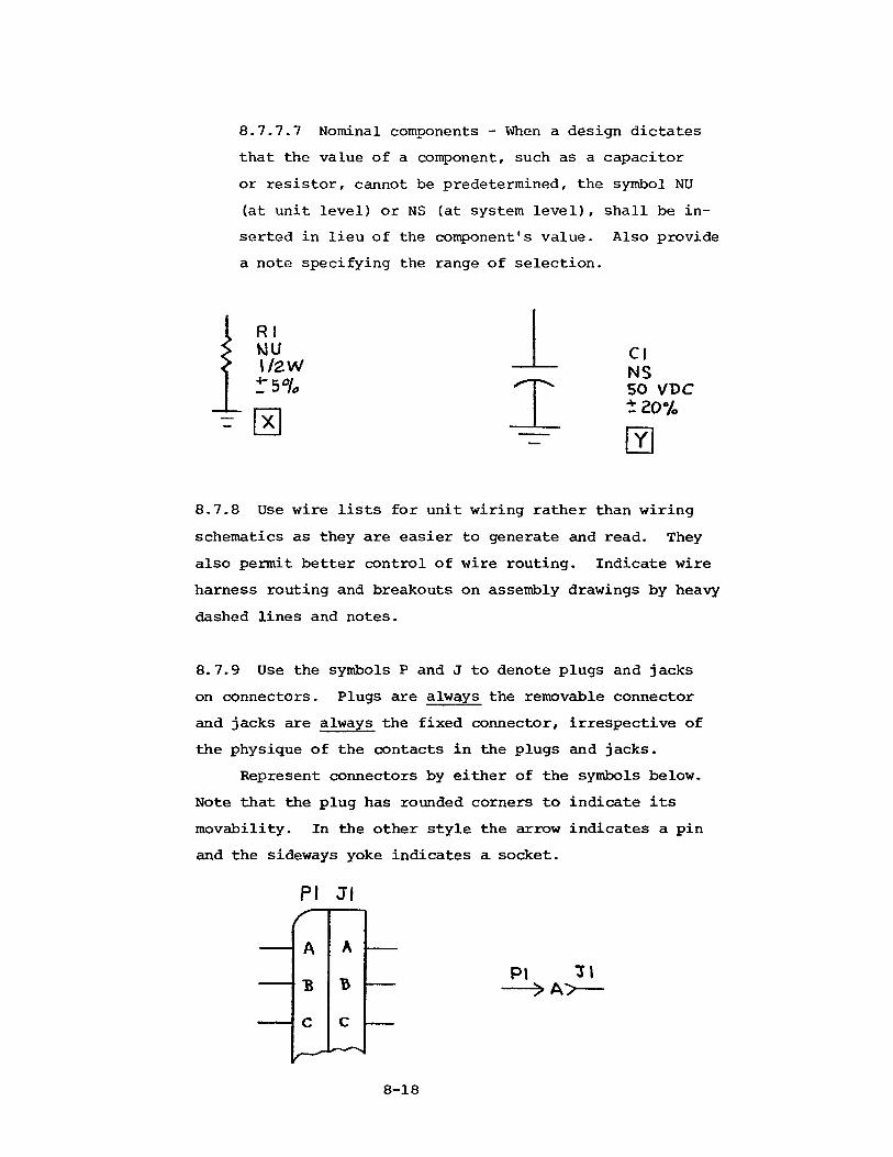
8.7.7.7 Nominal components - When a design dictates that the value of a component, such as a capacitor or resistor, cannot be predetermined, the symbol NU (at unit level) or NS (at system level), shall be inserted in lieu of the component's value. Also provide a note specifying the range of selection.
ClNS50 VDC 1 20%
m
8.7.8 Use wire lists for unit wiring rather than wiring schematics as they are easier to generate and read. They also permit better control of wire routing. Indicate wire harness routing and breakouts on assembly drawings by heavy dashed lines and notes.
8-7.9 Use the symbols P and J to denote plugs and jacks on connectors. Plugs are always the removable connector and jacks are always the fixed connector, irrespective of the physique of the contacts in the plugs and jacks.
Represent connectors by either of the symbols below. Note that the plug has rounded corners to indicate its movability. In the other style the arrow indicates a pin and the sideways yoke indicates a socket.
PI Jl
------ A A
"B
C C
8-18
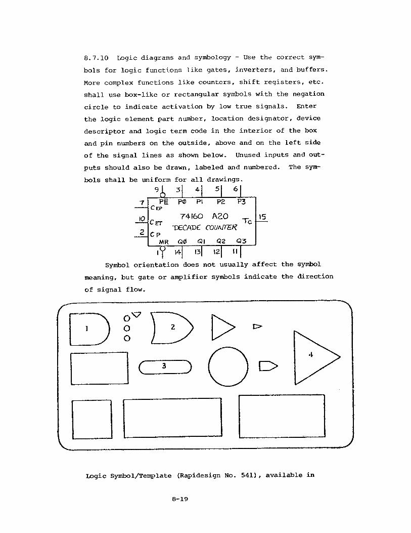
8.7.10 Logic diagrams and symbology - Use the correct symbols for logic functions like gates, inverters, and buffers. More complex functions like counters, shift registers, etc. shall use box-like or rectangular symbols with the negation circle to indicate activation by low true signals. Enter the logic element part number, location designator, device descriptor and logic term code in the interior of the box and pin numbers on the outside, above and on the left side of the signal lines as shown below. Unused inputs and outputs should also be drawn, labeled and numbered. The symbols shall be uniform for all drawings.
9 ^ 3 1 4 | 5 | 6 1
7
10
PE P0 PI P2 P3C ep74160 a eo
C ET Tc"D£CAD£ COUMTERCP
MR Q0 0 1 Q 2 Q 3
15
l y |4-| I3| I2| II
Symbol orientation does not usually affect the symbol meaning, but gate or amplifier symbols indicate the direction of signal flow.
Logic Symbol/Template (Rapidesign No. 541), available in
8-19

full, 3/4 size (shown), half size, 3/8 size or 1/4 size. 1 = And 2 = Or 3 = Time Delay 4 = Amplifier
Negation and exclusive OR - A small circle drawn at the point where a signal line joins a logic symbol indicates a logic negation.
To simplify schematics, signal paths may be delineated thus:
Signals may be assigned a number as shown in the example on the next page and run in a common path with a breakout downstream identified by the signal number.
TYPICAL LOGIC NEGATION
Input Side
Output
EXCLUSIVE OK SYMBOL
Single Channel n/
"n" = Number of Channels
2 Channel Multiple Channel vjth Takeoff
3 Channel
8-20

Signal wiring bulk on logic drawings can also be minimized by encoding terms with mnemonic names which then are placed adjacent to the pins they are connected to.
Note that the placement of logic symbols on a logic diagram does not control the actual wire routing of the interelement wiring; the routing is usually controlled by a wire list to minimize total run length, or control harnessing.

8.8 Wiring Harness and Cable Assembly Drawings
8.8.1 When large quantities are involved, a wiring harness assembly drawing symbolically depicting a group of wires bundled together in a specified configuration is required.This configuration contains unattached leads which are generally soldered or welded and is normally secured within a unit. See figures 8.8.1 and 8.8.2.
8.8.2 Draw all wiring harness drawings used as templates full scale on stable base material. Draw the harness outline to the approximate diameter of the finished harness.
8.8.3 Tolerances - Where dimensions are placed in the field of the drawing, show their tolerances to the nearest tenth of an inch.
8.8.4 Contour - Show all items attached to or located within the contour such as sleeving, connectors, sleeves or ferrules.
8.8.5 Revisions - Make all drawing changes of wiring harnesses to scale.
(a) Whenever runs are deleted from the harness, erase the breakouts, reference designators, and station numbers from the view.
(b) Whenever runs are added, draw the breakouts, apply proper reference designation, and assign the station numbers as follows: If there is a gap in the sequence of numbers, use the missing numbers; if there is no gap in the sequence of numbers, use the lower station number with a letter suffix (interim station number)i.e., 43, 43A, 43B, 44.
8-22
8.8.6 Show a lead breakout, reference designation, and station number for each unique lead termination on the drawing.
8.8.7 Unique stripping information may be indicated on the drawing either in the general notes or in a chart.
8.8.8 Add the notation "SHLD" to external shield lead breakouts. Add color notations to lead breakouts, when required.
8.8.9 Cable assembly drawings - A cable assembly drawing symbolically depicts cables normally used between equipments or units, and whose terminations are usually plugs, sockets, or connectors.
8.8.10 Wherever possible, structure cables to use simple single runs and avoid multi-breakout complex cables as they are difficult to fabricate and more liable to have wiring errors.
8.8.11 A cable assembly drawing maY drawn as a single line presentation as shown in figure 8.8 .1 (preferred) or in a more pictorial manner where required to depict assembly procedures.
8.8.12 Cable assembly overall dimensions - When the addition of overall dimensions is a critical requirement of the cable assembly drawings, position the connector views in line with, and adjacent to, the fabrication view so that dimensions can be illustrated as shown in figure 8.8.2.
8-23

D
P
Figure 8.8.1 EXAMPLE OF CABLE ASSEMBLY SINGLE LINE PRESENTATION
8-24

8.8.13 Cable assembly marking - Cable assembly drawings shall require each cable be properly marked with its reference designation (when applicable) and item identification. The drawing shall also indicate markings on all mechanically removable items such as lugs, pins, contacts, terminals, and connectors. Markers shall be identified by an item number callout (marker lengths and marking notes shall be added as applicable).
8.8.14 Tabulated cable assemblies - Cable assemblies having identical parts (connectors and wire) and identical connections but requiring different markings or lengths, may be tabulated.
8.8.15 General marking (reference designation, controland function identification, warning signs, etc.) - Whenever possible, general purpose marking shall be delineated at the detail (piece part) drawing level.
8.8.16 Reference designations - Reference designations, if required, shall be marked adjacent to each item and located in such a position as to identify the location of the item. Whenever possible, the marking must be visible in the item's assembled position.
a. Components and assemblies - The marking on the wiring side may include class letter "X" prefixing the reference designation of the mounted part for socket or plug-in items. The marking on the mounting or plug-in side shall only be the reference designation of the mounted item.
EXAMPLE OF COMPONENT REFERENCE DESIGNATION MARKING
8-25
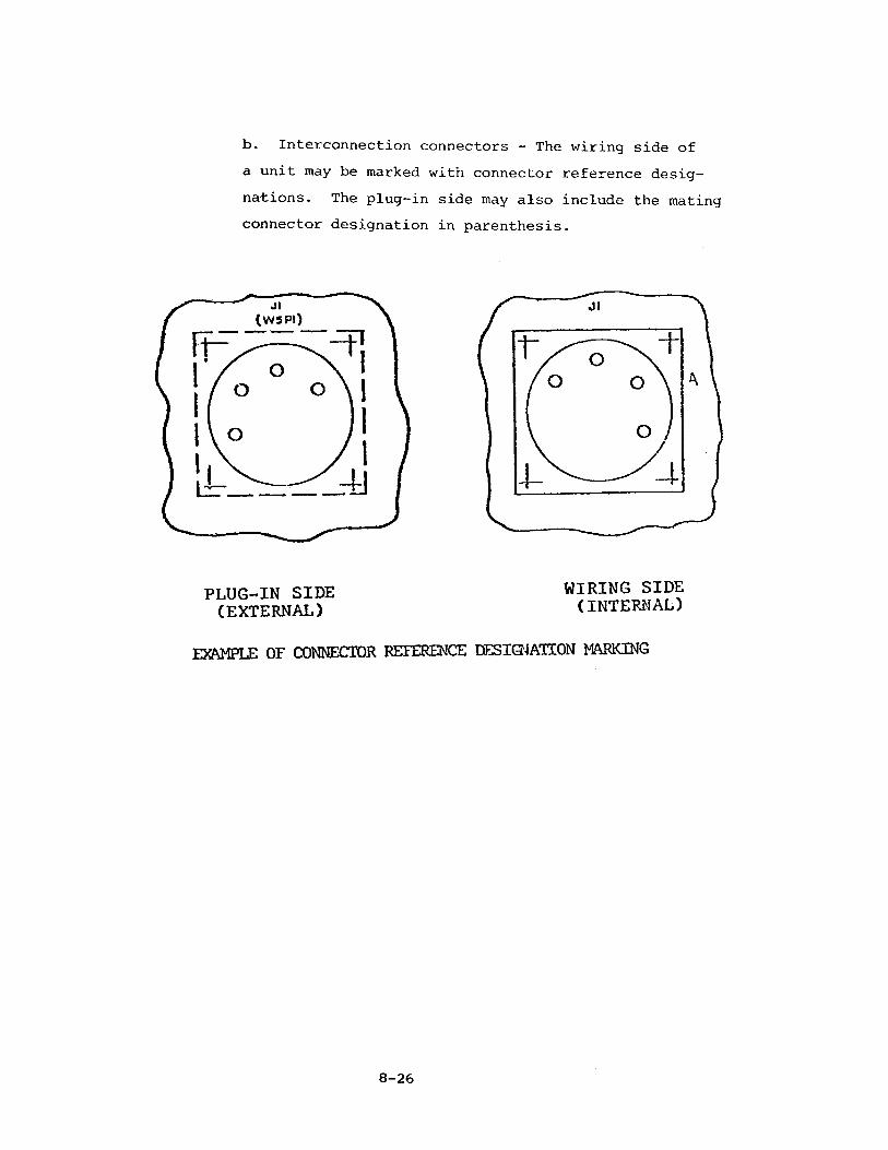
b. Interconnection connectors - The wiring side of a unit may be marked with connector reference designations. The plug-in side may also include the mating connector designation in parenthesis.
PLUG-IN SIDE (EXTERNAL)WIRING SIDE (INTERNAL)
EXAMPLE OF CONNECTOR REFERENCE DESIGNATION MARKING
8-26
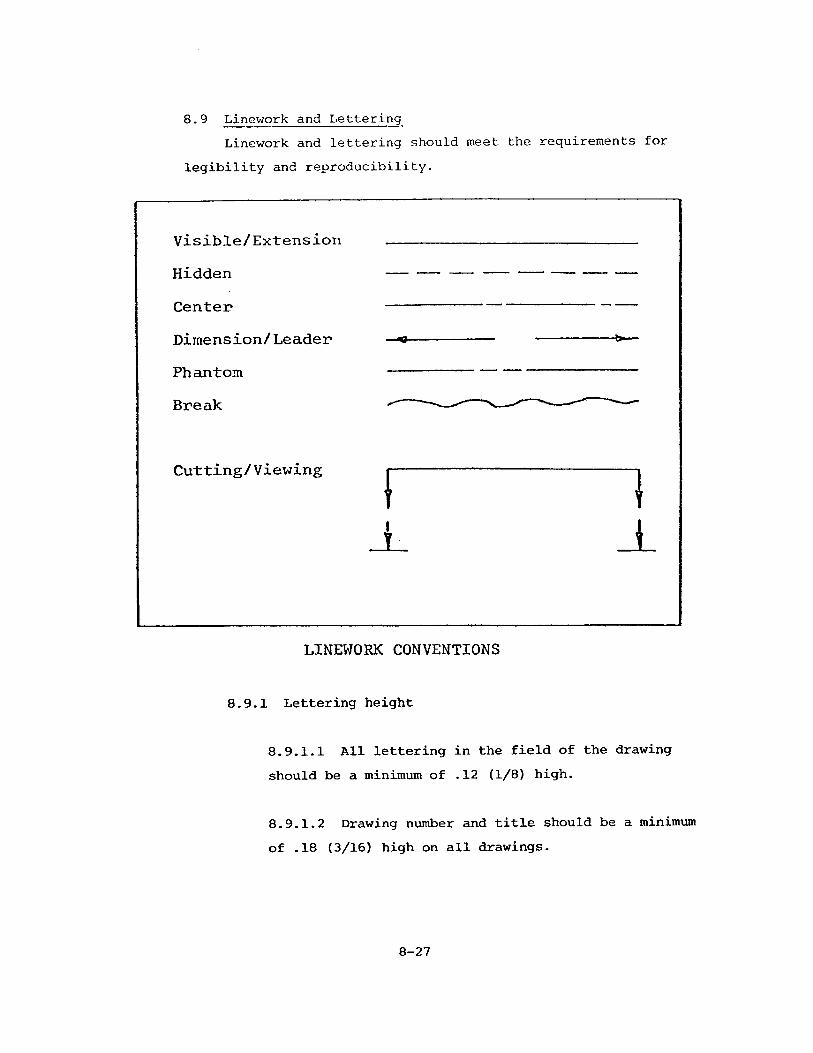
8.9 Linework and LetteringLinework and lettering should meet the requirements for
legibility and reproducibility.
LINEWORK CONVENTIONS
8.9.1 Lettering height
8.9.1.1 All lettering in the field of the drawing should be a minimum of .12 (1/8) high.
8.9.1.2 Drawing number and title should be a minimum of .18 (3/16) high on all drawings.
8-27

8.9.1.3 Typing and varitype lettering are permissible on the body of all drawing sizes, and may be used for the drawing number and title on A and B size drawings.
Isolated terminals - The location of isolated terminals shall be marked, if required, with reference designation "E" followed by a numeric character (e.g. El, E2, E3).
8-9.1.4 Control and functional markinga. Components mounted on the front panel of a cabinet which are visible while the equipment is in operation are normally marked with the function designation. Reference designations may be marked on the wiring side of a panel as follows:
CM S TEST POINTS
FRONT PANEL SIDE WIRING SIDE
EXAMPLE OF FUNCTIONAL MARKING
8-28
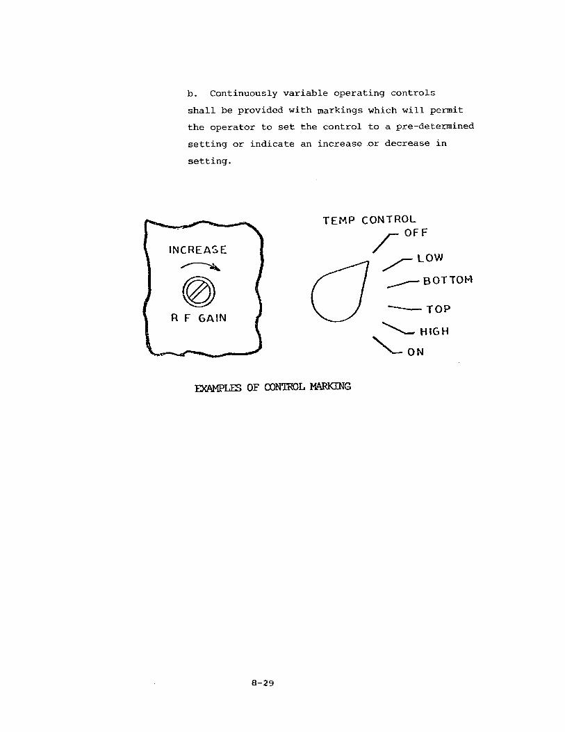
b. Continuously variable operating controls shall be provided with markings which will permit the operator to set the control to a pre-determined setting or indicate an increase or decrease in setting.
T E M P C O N T R O Ly - O F F
L O W
B O T T O M
O N
EXAMPLES OF CONTROL MARKING
8-29


9.0 VLA DOCUMENTATION/DRAWING SPECIFICATIONS
9.1 VLA SpecificationsThe following specifications are a collection of packaging,
drawing and notational conventions which have been in effect in the VLA project.
9-1

Interoffice
NATIONAL RADIO ASTRONOMY OBSERVATORYVLA PROJECT
MAGDALENA, NEW MEXICO 87825
To: VLA Electronics Staff, R. M. Mitchell, September 22, 1976Systems Integration, Synchronous Computer Div.
From: A. R. Thompson
Subject: NUMBERING SYSTEM FOR RACKS, BINS AND MODULES
Attached is a revised version of a specification written over two years ago. It has been updated to include all types of units now in used.
The only change in our current numbering system relates to the IF/LO racks in the central electronics room of the control building. These are to be known in the future as type D racks and individual racks will be designated by D followed by the serial number, which will run from 1 to 27.Up to now the designation has been W followed by the serial number. The letter N, E or W followed by a number will be an alternate means of designating individual racks, but the number will in the future be that of the associated waveguide channel. This second designation will not be applicable until a rack has been positioned in one of the thr.ee rows in the central electronics room.
I should like to request of the Charlottesville group that serial numbers of type D racks henceforth include the letter D instead of N, E or W. The bin type descriptions should also be marked on the bins before shipment from Charlottesville.
Please ensure that present usage and any future designations conform to the specifications.
ART:cb
Distribution:
D. S. Bagri A. Miller V. HerreroK. Barbier P. Napier L. BlankenshipC. Broadwell M. Ogai J. SpargoE. M. Caloccia J. Oty A. HerzogK. Clayton R. Schweigert B. G. ClarkB. Cohee R. Serna G. HuntD. Coombs P. Temple K. SowinskiL. D'Addario D. Weber P. DooleyW. Dundee J. Campbell M. FuscoF. Dunn G. BarrellR. Escoffier c. PaceJ. Guin R. HarrisS. Maas G. Patton
9-2
NATIONAL RADIO ASTRONOMY OBSERVATORY Post Office Box "O"
Socorro, New Mexico 87825
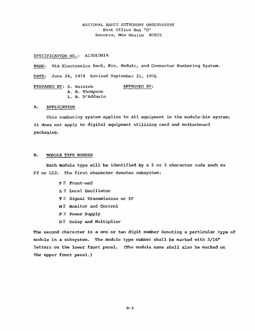
SPECIFICATION NO.: A13010N1A
NAME: VLA Electronics Rack, Bin, Module, and Connector Numbering System.
DATE: June 24, 1974 Revised September 21, 1976
PREPARED BY: S. Weinreb APPROVED BY:A. R. Thompson L. R- D ’Addario
A. APPLICATIONThis numbering system applies to all equipment in the module-bin system;
it does not apply to digital equipment utilizing card and motherboard packaging.
B. MODULE TYPE NUMBER
Each module type will be identified by a 2 or 3 character code such as F2 or L12. The first character denotes subsystem:
F = Front-endL = Local OscillatorT 5 signal Transmission or IFM= Monitor and ControlP = Power SupplyD-= Delay and Multiplier
The second character is a one or two digit number denoting a particular type of module in a subsystem. The module type number shall be marked with 3/16" letters on the lower front panel. (The module name shall also be marked on the upper front panel.)
9-3

C. MODULE SERIAL NUMBER
Each module will have a 2 or 3 character serial number such as Al or B13. The first character notes a particular version or revision; the second character is a consecutive serial number not affected by the revision letter (i.e., if 2 version A modules, Al and A2, were built the first revision B module would be labeled B3). The serial number shall be marked with 1/8” letters on the lower front panel.
D- RACK TYPE DESIGNATION
Letters are used to designate types of racks in the system as follows:A = Front-end Rack (antenna vertex room)B = IF/LO Rack (antenna vertex room)C = Pedestal Room Rack (antenna pedestal room)D = IF/LO Rack (control building, central electronics room)M= Master LO (control building, central electronics room)
One each of types A, B, C and D is required for each antenna.Racks and antennas will have serial numbers in the range 1 to 28. In
general racks located at antennas (types A , B and C) will be chosen so that their serial number is the same as that of the antenna. Racks of type D are not permanently related to a particular antenna, but are related by their location to a particular arm of the wye and waveguide channel number. Individual D racks can be referred to by arm (N, E or W) and channel number (e.g., W5) as well as by serial number.
E. BIN NUMBER
Bins will be lettered as follows:
Front-end RackIF/LO Rack at Antenna (top to bottom)IF/LO Rack at Control Room (top to bottom) Master LO Rack
Q , S , R T, U
9-4

F- SLOT NUMBER
Slots within a bin will be numbered 1 through 12 (1 through 20 for bin G which is extra wide) from left to right as viewed from front and right to left as viewed from rear. If a module occupies more than one slot width its location will be designated by the lowest slot number it occupies.
G. CONNECTOR AND PIN NUMBER
Plugs and jacks will be noted P or J, respectively, followed by a number which increases from top to bottom of the slot. For multi-pin connectors this will be followed by a dash and the pin number; i.e., Jl-42.
H. EXAMPLE
In most cases the complete number will not be necessary; i.e., we will refer to "Rack Bl", "Bin H" or "Module T2”. However, an example of a specific pin number is 27BH12Jl-42 which refers to antenna 27, rack B, bin H, slot 12, jack 1, and pin 42.
9-5
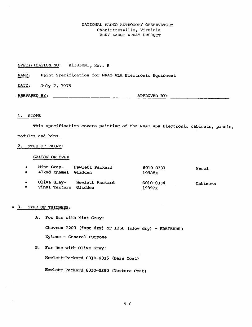
NATIONAL RADIO ASTRONOMY OBSERVATORY Charlottesville/ Virginia VERY LARGE ARRAY PROJECT
SPECIFICATION NO: A13030N1, Rev. B
NAME: Paint Specification for NRAO VLA Electronic Equipment
DATE: July 7, 1975PREPARED BY: __________________ APPROVED BY:
1. SCOPE
This specification covers painting of the NRAO VLA Electronic cabinets, panels, modules and bins.
2. TYPE OF PAINT:
GALLON OR OVER
* Mint Gray- Hewlett Packard* Alkyd Enamel Glidden
* Olive Gray- Hewlett Packard* Vinyl Texture Glidden
6010-033119988X6010-033419997X
Panel
Cabinets
* 3. TYPE OF THINNERS:
A. For Use with Mint Gray:
Chevron 1200 (fast dry) or 1250 (slow dry) - PREFERRED Xylene - General Purpose
B. For Use with Olive Gray:
Hewlett-Packard 6010-0035 (Base Coat)
Hewlett Packard 6010-0390 (Texture Coat)
9-6
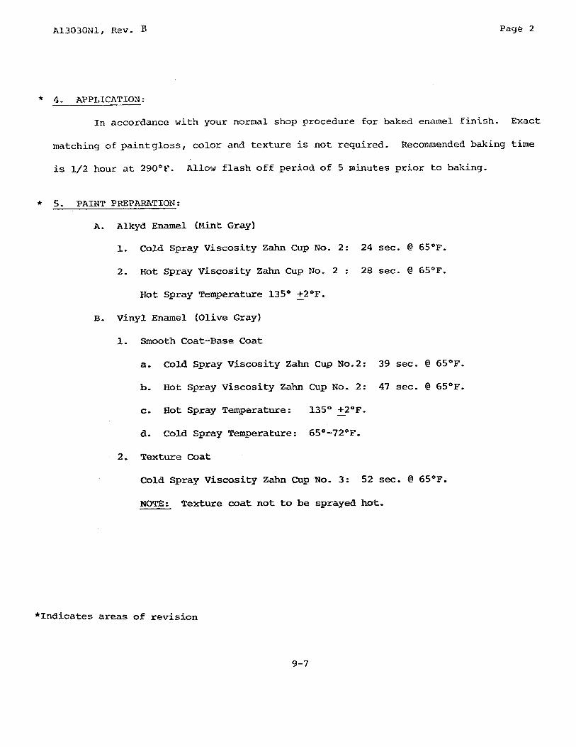
A13030N1, Rev. B Page 2
* 4. APPLICATION:
In accordance with your normal shop procedure for baked enamel finish,
matching of paint gloss, color and texture is not required. Recommended baking
is 1/2 hour at 290°F. Allow flash off period of 5 minutes prior to baking.
* 5. PAINT PREPARATION:A. Alkyd Enamel (Mint Gray)
1. Cold Spray Viscosity Zahn Cup No. 2: 24 sec. @ 65°F.
2. Hot Spray Viscosity Zahn Cup No. 2 : 28 sec. @ 65°F.
Hot Spray Temperature 135° +2°F.
B. Vinyl Enamel (Olive Gray)
1. Smooth Coat-Base Coat
a. Cold Spray Viscosity Zahn Cup No.2: 39 sec. @ 65°F.
b. Hot Spray Viscosity Zahn Cup No. 2: 47 sec. @ 65°F.
c. Hot Spray Temperature: 135° +2°F.
d. Cold Spray Temperature: 65°-72°F.
2. Texture Coat
Cold Spray Viscosity Zahn Cup No. 3: 52 sec. @ 65°F.
NOTE: Texture coat not to be sprayed hot.
*Indicates areas of revision
Exact
time
9-7

NATIONAL RADIO ASTRONOMY OBSERVATORY Charlottesville, Virginia VERY LARGE ARRAY PROJECT
SPECIFICATION NO: A13050N2 Revision A
NAME: VLA Module System Dimension Standards DATE: August 5, 1974
PREPARED BY: _______________ ___________ APPROVED BY:
1. Vertical Dimensions, HeightsBin Spacing 8.750Bin-to-Bin-Gap .030Bin Height 8.720Module Hole Spacing 8.220Horiz. Bar to Horiz. Gap 7.720Runner-to-Runner *7.387 +0.005Runner-to-Guide Gap .040 _+.022Guide-to-Guide *7.346 +^.005Module Outside Height 7.220 +0.010
XUA Inside Clear 5.720XUA Vent-to-Vent 6.410XSA Inside Clear 6.470Bottom Guide Surface toRear Panel Bottom * .067 ___— • 00b
Bin Rear-Panel Lower Mounting Hole to Module Rear-Panel .686 +^010
2. Horizontal Dimensions, WidthsBin Panel Width *19.000 +.030Rack Hole Spacing 18.310 +.030Bin Outside 17.495 +.030Bin Inside 16.995Bin Panel Space 16.745IX Spacing * 1.395 +^.005IX Panel Width * 1.385 +.005IX Module, Outside * 1.360 +0.0051UA Inside Clear 1.172
*Indicates critical dimension, 100% inspection9-8
Specification No. A13050N2 -2
(cont.)ISA Inside Clear 1.1102X Spacing * 2.790 +^.0052X Panel Width * 2.730 + .0052X Module, Outside * 2.760 0102UA Inside 2.510 +_.010NX Spacing *Nx 1.395NX Panel Width *Nx 1.395 -.010NX Module Width *Nx 1.395 -.030NUA Inside, N >_ 2 Nx 1.395 -.280Front-Panel Gap .010 .010Module Gap -030 + .010Runner Width * .250 +_ .008Guide Slot Width * .275 .005Horizontal Guide Gap .025 +. -013
Depth DimensionsBin Overall, Excluding Connectors 20.426Front Panel .125Rear Panel, IUA .125Panel-to-Panel, Bin Inside *20.176 ^qqq5
+0.000Module, Inside-Front, Outside-Rear Panel *19.312
Bin-to-Module Rear Panel Gap * .864 _
- 0.010
+ .015
OMQ Connector Plate Offset .464 HK.005+ .020
015OMQ Connector Panel Gap * -400
XUA Module Inside 19.187Rear Panel ISA .250XSA Module Inside 19.062
4. Countersink for straight internal threads shall be 85° ± 10° to depth of major diameter of thread-
♦indicates critical dimension, 100% inspection9-9

NATIONAL RADIO ASTRONOMY OBSERVATORYCHARLOTTESVILLE, VIRGINIAVERY LARGE ARRAY PROJECT
SPECIFICATION NO.: A13050N3 REV. A
NAME: Engraving Specification for NRAO VLA Electronic Equipment DATE: August 9, 1974
PREPARED BY; _______________ _ APPROVED BY:
1. SCOPE
This specification covers engraving of the NRAO VLA electronic module
front and rear panels. Contents of this specification must be called out on
detail drawings that require engraving.
2. ENGRAVED CHARACTER SIZES
(a) Type: Gorton normal or condensed, or equivalent (as specified on panel drawings)
(b) Height: 3/16", 1/8", and 3/32" (as specified on panel drawings)(c) Line Width: .020" ± .002"
(d) Type of Cutter: "V" groove
3. FILLING
Groove shall be filled with black epoxy ink.
(See Drawing A13050M43)
9-10

\/S H IG H ( E X A M P LEI',
I.F . R ECEIVER)
3 / l fe H I £ H ------- y. ' ' t ^ A V .P L E : l _ | ) \
.03-.0 3 - --
[TYPE [1ser.no. \
<L
uJ ^ Js S < -*9 dc 2 u.
NO
X
0 52 -5 *•4. o
{£(*< 0 vD -J . u* 2 di
^ .tlJ Ld R ^ Icct! »d h- < k 2 >
"IO UJ < J
v/>2°A- «
X?U *Ijl'-nT*OtvCJ_ -JvDt** u1
CD
<
o
Q ^ d c$ 2 0
O f-_ | Z << o >z h d :O h— LU rzcoco 5 < m^ o
q _ c : o - 3 u j o > -
> _ J <
uC- <. O
-7 -J LJ2 j 2£ (V^
OvPoC2k
D h J 2 $3^ O
h O CI------ 1—_ IU J .
I /a H l^H C EXAMPLE: A ) ) KjOT t o BE EMGRAsVED
>UJcc*1*samart
z <3
OEU.ICSuaw2
9-11
NATIONAL RADIO ASTRONOMY OBSERVATORY Charlottesville, Virginia VERY LARGE ARRAY PROJECT
SPECIFICATION NO: A13230N1NAME: Assembly of UT-141A .141 Semi Rigid Coaxial Cable to Type OMQ Connector
DATE: June 27, 1975PREPARED BY: ______ APPROVED BY: _________ _____
1. GENERALTo provide a step by step procedure for proper installation of the .141
DIA Semi Rigid Coax to Omni/Spectra Connector nos. OMQ 3033-75 and OMQ
3043-75. To identify component parts of connector assemblies and desig
nated tooling used to complete the cable/connector installation.
2.0 SPECIAL TOOLING REQUIRED:2.1 Center Contact Crimp Tool: *0SI T-6873-2 Common
2.2 Center Contact Positioner: OSI T-6873-7 Common
2.3 Fixture Base: OSI T-6869-1 Common
2.4 Cable Clamp Insert: OSI T-4700-1 Common
2.5 Locator Screw: OSI T-6874-2 (#3033-75 only)2.6 Locator Screw: OSI T-6872-2 (#3043-75 only)
2.7 Assembly Fixture: NRAO #C13050T1-1 (#3033-75 only)
2.8 Assembly Fixture: NRAO #Cl3050Tl-2 (#3033-75 only)
2.9 Assembly Fixture: NRAO OSI T-4554
3.0 OMQ 3033-75A Connector
*Omni/Spectra Incorporated
9-12
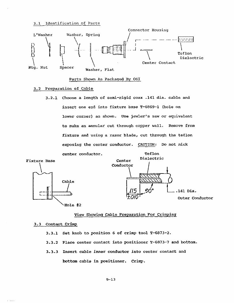
3.1 Identification of PartsConnector Housing
L 'Washer Washer, Spring
IMtg. Nut
lf\
Spacer
V J
ANVff—
n ® \£ p
TeflonDielectric
Center ContactWasher, Flat
Parts Shown As Packaged By OSI
3.2 Preparation of Cable3-2.1 Choose a length of semi-rigid coax .141 dia. cable and
insert one end into fixture bas6 T-6869-1 (hole on
lower corner) as shown. Use jewler's saw or equivalent
to make an annular cut through copper wall. Remove from
fixture and using a razor blade, cut through the teflon
exposing the center conductor. CAUTION: Do not nick
center conductor.Fixture Base
\Center
Conductor
\Cable
L
TeflonDielectric
,(15 \JX>'t o i o 7^
.141 Dia.Outer Conductor
Hole #2
View Showing Cable Preparation For Crimping
3.3 Contact Crimp3.3.1 Set knob to position 6 of crimp tool T-6873-2.
3.3.2 Place center contact into positioner T-6873-7 and bottom.
3.3.3 Insert cable inner conductor into center contact and
bottom cable in positioner. Crimp.
9-13

3.4 Installation of Cable Sub-Assembly to Connector Housing
3.4.1 Remove teflon dielectric from connector housing.
3.4.2 Insert aluminum spacer NRAO C13050T1-1 into contact end
of connector housing replacing teflon. (After soldering,
spacer must be removed.)
3.4.3 Using fixture base T-6869-1 and locator screw T-6874-1,
insert the crimped contact end of cable through the
connector housing, as the opposite end is aligned with
the locator screw. Allow the cable to be clamped between
jaws T-4700-1 while locator screw is tightened snuggly
capturing the whole assembly. Note the illustration on
NRAO drawing C13050T1-1 for additional details.
3.4.4 Burnish area to be soldered using fine sand paper. Then
aPPly non-corrosive flux in areas to be soldered. Pro
ceed to solder the annular surface at point of insertion
into the connector housing using rosin core solder, 60%
tin, 40% lead. Allow assembly to cool before removing
from fixture. Remove aluminum spacer. Soldering mode is complete,
3.5 Procedure for Installing Teflon Dielectric
3.5.1 Assembly fixture, NRAO C13050T1-2 is used in this procedure to align the contact end of connector housing so
the dielectric sleeve may be seated into cavity around
contact without any damage to teflon or the center contact.
3.5.2 Engage knurled knob to the threads of the connector hous
ing and tighten the assembly until it becomes rigid.
9-14
3.5.3 Place teflon dielectric into opening of mandrel C13050T1-2-1
and using plunger C13050T1-2-2 to force teflon down into
cavity surrounding contact in connector housing- Refer
to NRAO drawing C13050T1-2 for complete illustration.
3.5.4 Remove connector from fixture and inspect the dielectric-
If properly seated, the housing shoulder should be just
visible to the eye. Connector should now be ready for
installation into racks or modules.
3.5.5 Use inspection gage NRAO # C13050T3, (see dwg. for inspection procedure).
4.0 OMQ 3043-75 CONNECTOR
4.1 Identification of Parts
■ ■ m i
Housing Sub-AssemblyInternal Tooth
Lockwasher
Teflon Dielectric Center Contact (female)
K
Locknut
Parts Shown as Packaged By OSI
4.2 Preparation of Cable:4.2.1 Choose a length of semi-rigid coax .141 diameter cable
and insert one end into fixture base T-6869-1 (hole on
lower comer) as shown. Use small jewler's say or equi
valent to make an angular cut through copper wall. Re
move from teflon exposing the center conductor.CAUTION: Do not nick center conductor.
9-15
4.3.1 Set knob to position 6 of crimp tool T-6873-2.
4.3.2 Place center contact into positioner T-6873-7 and bottom.
4.3.3 Insert cable inner conductor into center contact and bottom cable in positioner. Crimp.
Ari__Installation of Cable Sub-Assembly to Connector Housing
4.4.1 Remove teflon dielectric from connector, housing.
4.4.2 Insert aluminum spacer NRAO drawing C13050T1-1-6 into
contact end of connector taking the position of the
teflon. (After soldering, spacer must be removed.)4.4.3 Using fixture base T—6869—1 and locator screw T-6872-2,
insert the crimped contact end of cable through the
connector housing, as the opposite end is aligned with
the locator screw. Allow the cable to be clamped between
jaws T-5700-1 while locator screw is tightened snugly
capturing the whold assembly. Note the illustration on NRAO drawing C13050T1-1 for additional details.
4.4.4 Burnish area to be soldered using fine sand paper. Then
apply non-corrosive flux in areas to be soldered. Proceed to solder the annular surface at point of insertion
into the connector housing. Also solder shoulder as this tends to come off connector when put into service., using rosin core solder, 60% tin, 40% lead. Allow
9-16
4.3 Contact Crimp:

assembly to cool before removing from fixture. Remove
aluminum spacer. Soldering mode is complete.
4.5 Procedure for Installing Teflon Dielectric4.5.1 Assembly fixture OSI T-4554 is used in this procedure
to align the contact end of connector housing so the dielectric sleeve may be seated into cavity around contact
without any damage to center contact or to grip fingers
around teflon. See illustration below.
INSERT DIELECTRIC BUSHING INTO SUB-ASS EM BUY
S U B - A S S E M 8 L Y
Secure dielectric insert tool housing to threads of connector.
Remove plunger from tool housing.Insert dielectric bushing into center hole of tool housing.
Push firmly with plunger until flange bottoms on tool
housing shoulder.
9-17
4.5.2
4.5.34.5.44.5.5

9.2 Module Type/Name ListThe following defines the official module types and names
at the date of January 1, 1978.
9-18
To:
From:
Subject:
Interoffice
National Radio Astronomy ObservatoryVery Large Array
January 5, 1978VLA Electronics Staff, R. M. Mitchell, S. Weinreb, V. Herrero
A. R. Thompson
Module Names
The following is a revision of my memorandum of January 28, 1977 which listed the type numbers and names of modules. All new modules resulting from the latest system modifications are included.
Dl SamplerFl Bias ControlF2 Upconverter PumpF3 17-20 GHz L.O.F4 Frequency ConverterF5 Front End ControlF6 RF SplitterF7 Front End IF FiltersF8 IF OffsetLI 5-50 MHz VCXOL2 50 MHz Harmonic GeneratorL3 L.O. TransmitterL4 L.O. ReceiverL5 L.O. ControlL6 2-4 GHz SynthesizerL7 Fringe GeneratorL8 Timing GeneratorL9 Central L.O. ReceiverL10 Central L.O. TransmitterLll Central L.O. ControlL12 Master L.O. OffsetLI 3 600-1800 MHz MultiplierL14 Central L.O- FilterL15 Master L.O. Phase-LockL16 Synthesizer ControlL17 Synthesizer Phase-LockL18 Variable Frequency DriverL19 Master L.O- DriverL20 Master L.O. ControlL21 Synthesizer Phase-Lock Emergency PowerL22 Modem Offset Oscillator
9—19

Ml Data SetM2 Data TapM3 Central BufferM4 Antenna BufferH5 Command SimulatorM7 Focus/Rotation ControlM8 Focus/Rotation Power SupplyPI to P5 Power SuppliesT1 ModemT2 IF CombinerT4A, T4B L.O. Offset (to be replaced by T4: IF Converter in future r e t r o f i t )T5 IF ReceiverT6 IF Control
ART/drg
9-20
9.3 Plug In Wire Wrap Board ConventionsFigure 9.3 shows the format conventions for the plug in
wire wrap boards which are used in L.O. modules and the Delay- Multiplier system. Two sizes of boards are used which differ only in size; the larger size is shown in 9.3.
9-21
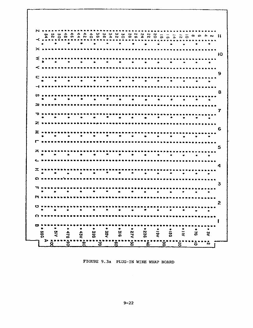
JNJ ................................................... ... ............................................................ ............................ ...O i O l O ^ ^ - f t i A O l W O I O I O I M M r O M f O - - _ ~ ^ rv_ I,^ js.rjOCDO’ - ^ ^ O O o x i r o o O c i ^ n O c j D)^ w O w 11
.............................. ................................. ......10
^ - * ................ ... ....................................... ... ............................................................ ............................... ... ........................
< ..............................................................9c: ................................ .........................
8to
7
z ....................................... ..6
5# * # # # • • • • • • • •
AX ......................................................... ...........• • • • •
3
.............................................................. ... ......................................................... .......................................... ...2
O • m m m m m m m m m m m m m m m m m m m m m m m m m m m m m m m m m m m m m m m m m m m m w m m m m m r n m m m • • • • • • • • • • • • • •
I• • • • • • • • • • » • « •« 5 s W ^ S < c , <o <* o < c > < ° < Cl < ° v
o g o w I
FIGURE 9.3a PLUG-IN WIRE WRAP BOARD
9-22
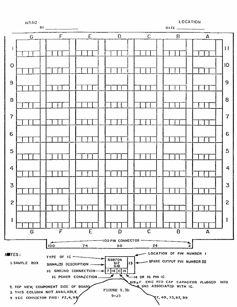
BYNRAO LOCATION
DATE ______________ _
D C B A
1
0
9
8
7
6
5
4
3
2
I
M ITES:
E E
D B
n
r n
T T
A
100 74100 PIN CONNECTOR
5 0 24
TYP E OF 1C
I-SAMPLE BOX SIGNAL(S) d e s c r ip t io n
1C GROUND CONNECTION
1C PCWER CONNECTION
'L TOP VIEW, COMPONENT SIDE OF BOAR
3. T H IS CO LUM N NOT A VAILABLE
4 7C C CONNECTOR PINS'- P 2 .4 , 9
N 8870AGI7GI8
13
7 14 C 14
i f
10
9
8
7
6
5
4
3
2
LOCATION OF PIN NUMBER I
. SPARE OUTPUT PIN NUMBER (S)
14 OR 16 PIN 1C 019 M F ERIE RED CAP CAPACITOR PLUGGED INTO
GND. ASSOCIATED W ITH 1C.
7. 49, 73,97, 99

RE WRAP—v =»SN R O W S \
R [> ^ A P —' M -13-R5
PiN 1C ACJNG
4 P IN IC- PACING
18 P IN IC- SRACING
[6 PIN IC- SPACING
14 PIN IC- SPACING
8 PIN 1C* SPACING
6 P IN !C- SPAC1NG
COLUMN-
NOTES:1 .2.3.4.5.6.
\NRAO CDP201
\ tvlN N N W N ----------—
/a o> ^ n 11-<X
< c: -H cn 33 U 2 .
• • • • m • m o #* * • *
------- - c B J .............. * ..............
tC Pfl FOR ™ SPACtN
10
«ROY
s l .
K D0>» £ , rv> c d
^ • Ol • OJ • |\ ) ■^ o Oi N 03
Dro o ro o -£> o
A
r~~\ C ROY / FOR
SPAC1 USE R( INCLOSED BRACKETS
•M IX E M >exam ® : :WITH EA- : • ON ITS OV PARTI® SPACIB
D C B A 7CD 0> Ol ,ro
ro ao ro CO • 4V»
E D | C B A■20 PI* SPACING
6, l
/-POWER PI? / COLUMNS
(A T « U
POWNUM I
vcc S
£X. Oo 03o o oo Olo -c*o OJo roo ro
COMPONENT SIDE OF BOARD SHOWNTHE CDP202 BOARD HAS ONLY 5 IC ROWS AVAILABLE INSTEAD OF THE 11 IC ROWS SHOWN.Vcc PLANE I/O CONNECTIONS: 2, 4, 98, 100 IGND PLANE I/O CONNECTIONS: 1, 3, 27, 28*, 49, 50* ,‘ 73, 74* 97, 99: 6 & 14 PIN ICs ARE ON SAME SPACING I8 & 16 PIN ICs ARE ON SAME SPACING !* GND BUS CONNECTIONS ONLY.
NO P.C. CONNECTIONS ON(SHEET I OF 2)
A ADDED 9 - 2 5 - 7 3 JE
B .3 0 0 WAS .0 3 0 .6 0 0 WAS .030
1-17-74 JE
C ADDED 9 -1 9 -7 4 SS&
DCHA.NGE0 i600 SPACING NOTATION 10-10-74 SSR

-c
X
&' ^ W 0 ° C1 ^ r j 0 ° C > A W 0 o C>-J‘ N 0 O D A W 0 1 */
y
o• M t» in u » iK i !TYPE 1 J69k n a U u » o
trf _cr> Oi0tVJ M
CD
Htlti ft fil Gis m u si t*^T3L K
» » > ■ »» » >| b |» >i »1»J i o -&■ « -P> » O l • OJCD ^ O O' N
H *►»»•»**ro® roCD Jv
B
cn.ro
4kCD
-P>,-F>
4*O
O l o O
OJro r o
CD
9 » t> » »X b k N O ■
9 a •4* Ol
-J Ol (Oo < oo oo ___Q_
•an****n ,4U PJN» • » M t> n R K
r\><
10;
"\9 ::
JV> ■o
D» S» m *»
B AJ8
F%» » !*»»»
ro •o ____
"3J m r m
D » » H «i©■ ©
B A
A
roo
5■\
fr» <X>
I K K * & m Is m » « • • aC 14 R 14v pjjvj j L ) p i n
» » » ■ P» PIN. » » ( • » *
rooto
o<
cno
-Jo oJ2. 8 s oio roo w
1C ROW NO * 7 .300 5 PACK
1C RG7/S / .600 SPACIJ
USE ROW NC INCLOSED Bj BRACKET l
40 PIN »e SPACING
-M INDICA PIN NC LOCAT
POWER PI -COLUMNS (A THftU C
p o w e r p :/NUM BERS
SEE NOTES ON SHEET 1 (FIGURE 3).
WIRE WRAP BOARD 1C LAYOUT (s h e e t 2 o f 2)
©

-26
Wire Wrap Printed Circuit Board Conversion Chart February 23, 1972
16-PIN CHIP
NRAO
V game as Wire Wrao Row A ** i i"; ICC
Examples;XC Wiring List No,
2C45E122CV7FGP15
P.C. Wire Wrap No.E23K42D19VP55GA15
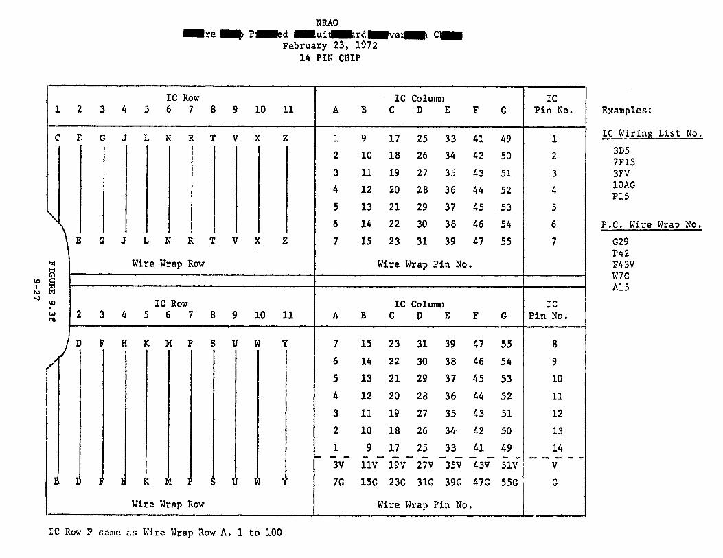
-27
February 23> 1972 14 PIN CHIP
NRAO
IC Row P same as Wire Wrap Row A. 1 to 100

-28
WIRE WRAP PRINTED CIRCUIT BOARD CONVERSION CHART September 4, 1973
18 Pin Chip
NRAO
EXAMPLES:IC Wiring List No.
2C45E122CV7EGP15
P.C. Wire Wrap No.E24K47D19VP47GA15

9.4 Monitor and Control System Notational ConventionsThe Monitor and Control System Module package design uses
wire wrapped logic connector boards which hold up to 30 fourteen or sixteen pin logic elements. Up to six of these 30 chip connector boards are used in a given module and are designated A through F starting from the rear panel as shown in Figure 5.2. Logic elements on the logic diagrams use a location designation based upon the board designator (A through F) and chip location (marked 1 through 30) on the board. Thus, A24-13 designates pin 13 on a logic chip located on board A, chip location 24. This notation is used on the wire lists and is prefixed by an X which is an ANSI convention for a plug-in socket. When fourteen pin chips are inserted into the sixteen pin sockets the logic element pins 8 through 14 are renumbered 10 through 16 on the logic diagrams. Pins 1 through 7 are unaffected in this case, but pins 7 and 8 are interconnected by a jumper wire to provide logic ground to the chip. Pins 8 and 16 on the connector board are committed to logic ground and +5 volts respectively.
Wire strings are designated by a unique signal name based upon the logic diagram sheet number and the location designation of the signal source that drives the string. The first character of the signal name is alphabetic and designates the logic sheet; thus, signal CD1306 is generated by logic gate D13, pin 6 on sheet 3 (i.e. , C).
There are four wire list formats for the Monitor and Control modules; these are the Master, Hand, Machine and Connector lists. The Master Wire list contains all the wiring in the module, but the Machine and Hand Wire lists are subsets of the Master Wire list and describe two separate classes of wiring: the Machine (levels 1 and 2) and Hand (level 3 and power wires). Machine wires are levels 1 and 2 interconnections (only) on the logic connector boards and are machine-wired. Hand wire level 3 wire wrap wires are used for I/O wires between the logic connector
9-29
boards and the I/O connectors and may be either machine-wired or hand-wired. An "H" and "M" in the wiring input data designate Hand and Machine Wire classes.
The Connector Wire list is a snapshot of each logic connector and shows the Signal Name and the "From" and "To" points in the string.
9.5 Drawing Listing and Parts Listing Coding FormsFigure 9.5a depicts the Drawing Listing coding format. This
data is sorted by a listing program to produce a listing of drawings by module. At present (1/1/78) this program resides in the CV 360, but it is planned to eventually implement it on the DEC-10 System.
Figure 9.5b depicts the Parts Listing coding format. This data is sorted to produce a collated listing of module parts versus quantities required. This program also resides in the CV 360 but has been implemented in a simplified form in the Tech 360 and is being altered to operate in the Dec-10 System.
9-30

DRAWING LIST CODING FORMS
Column No. Description1 - 3 Module number5 - 2 0 Drawing number and -X number
plus - (module number) if a common part
21 Revision letter (if none -)22 - 24 Day of year (1 to 365)25 & 26 Last 2 numbers of year (76)29 •30 - 54 Title55 '57 Number of sheets59 + Drawing microfilmed with master in CV
- Drawing not microfilmed with master in CV A Drawing microfilmed with master in NM B Drawing not microfilmed with master in NM
61 - 66 Cost in dollars and cents with decimalpoint in column 64 (if no cost use 0.00)
68 Key 1 (used to produce module drawing list)70 Key 2 (used to group items for procurement)
FIGURE 9.5a DRAWING LIST CODING FORMS
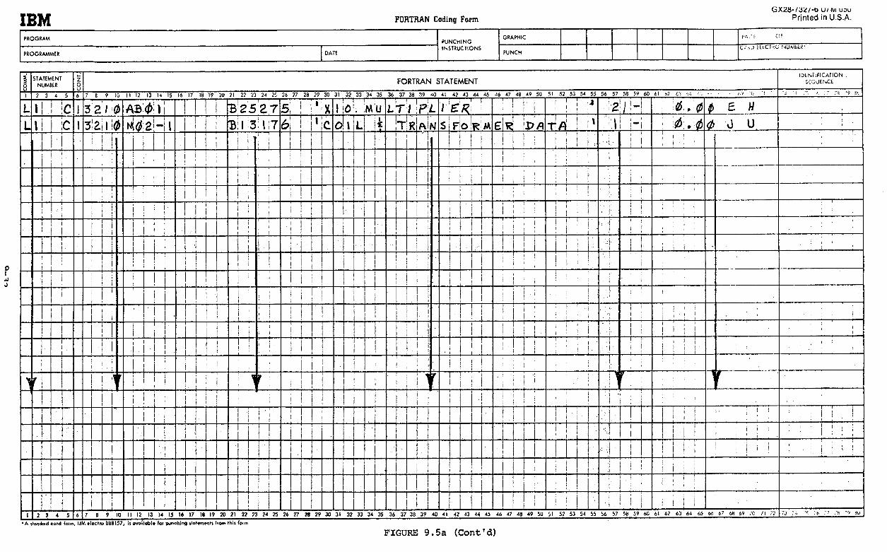
IBM FORTRAN Coding FormGX28-/y /-0 u/ rvi uou
Printed in U.S.A.
P R O G R A MP U N C H IN GIN S T R U C T IO N S
G R A P H IC O F
PRO GRA M M ER DATE PU N C HC / m J c L iiC T s O N U M U ER1
FIGURE 9.5a (Cont’d)
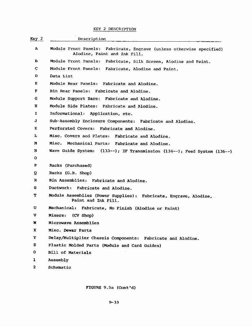
KEY 2 DESCRIPTION
A Module Front Panels: Fabricate, Engrave (unless otherwise specified) Alodine, Paint and Ink Fill.
B Module Front Panels: Fabricate, Silk Screen, Alodine and Paint.C Module Front Panels: Fabricate, Alodine and Paint.D Data ListE Module Rear Panels: Fabricate and Alodine.F Bin Rear Panels: Fabricate and Alodine.G Module Support Bars: Fabricate and Alodine.H Module Side Plates: Fabricate and Alodine.I Informational: Application, etc.J Sub-Assembly Enclosure Components: Fabricate and Alodine.K Perforated Covers: Fabricate and Alodine.L Misc. Covers and Plates: Fabricate and Alodine.M Misc. Mechanical Parts: Fabricate and Alodine.N Wave Guide System: (133— ); IF Transmission (134— ) ; Feed System (136— )0
P Racks (Purchased)Q Racks (G.B. Shop)R Bin Assemblies: Fabricate and Alodine.S Ductwork: Fabricate and Alodine.T Module Assemblies (Power Supplies): Fabricate, Engrave, Alodine,
Paint and Ink Fill.U Mechanical: Fabricate, No Finish (Alodine or Paint)V Mixers: (CV Shop)W Microwave AssembliesX Misc. Dewar PartsY Delay/Multiplier Chassis Components: Fabricate and Alodine.Z Plastic Molded Parts (Module and Card Guides)0 Bill of Materials1 Assembly2 Schematic
Key 2 ___________ Description ______________________________________
FIGURE 9.5a (Cont*d)
9-33
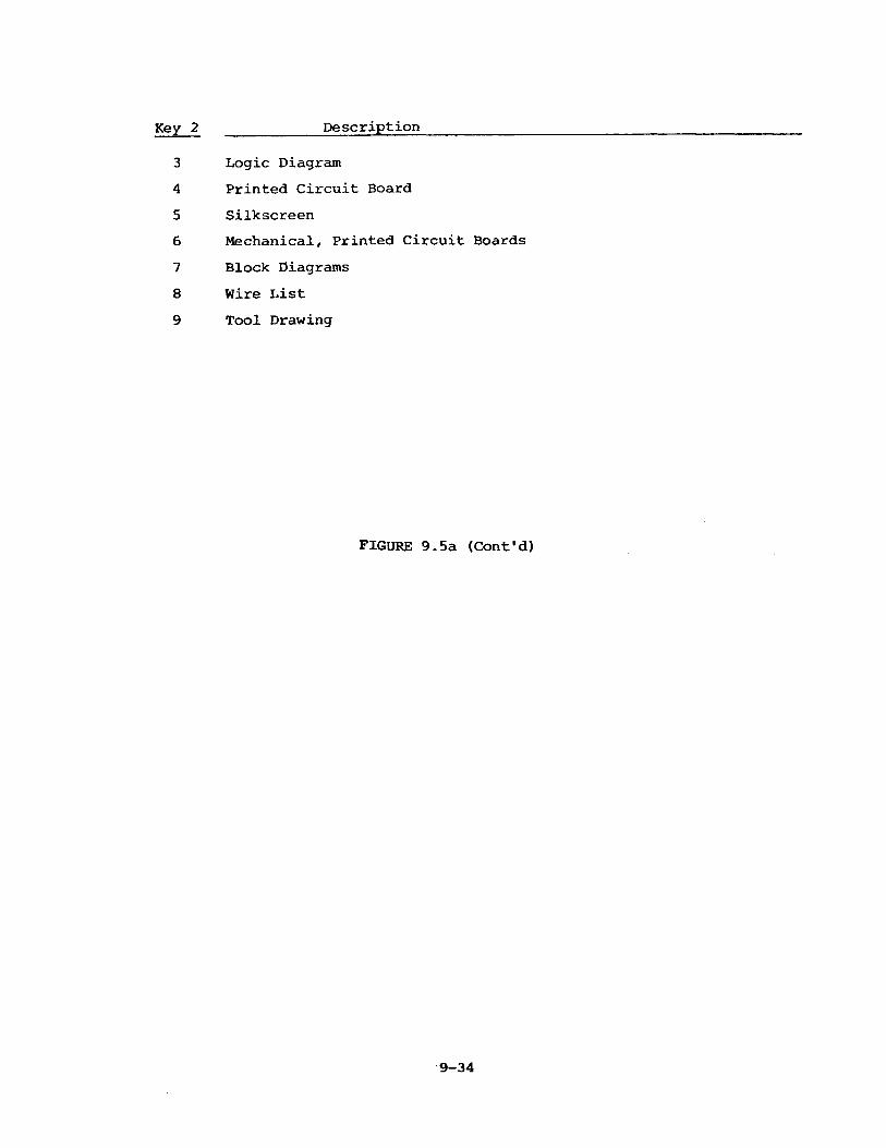
Key 2 Description
3 Logic Diagram4 Printed Circuit Board5 Silkscreen6 Mechanical, Printed Circuit Boards7 Block Diagrams8 Wire List9 Tool Drawing
FIGURE 9.5a (Cont'd)
9-34
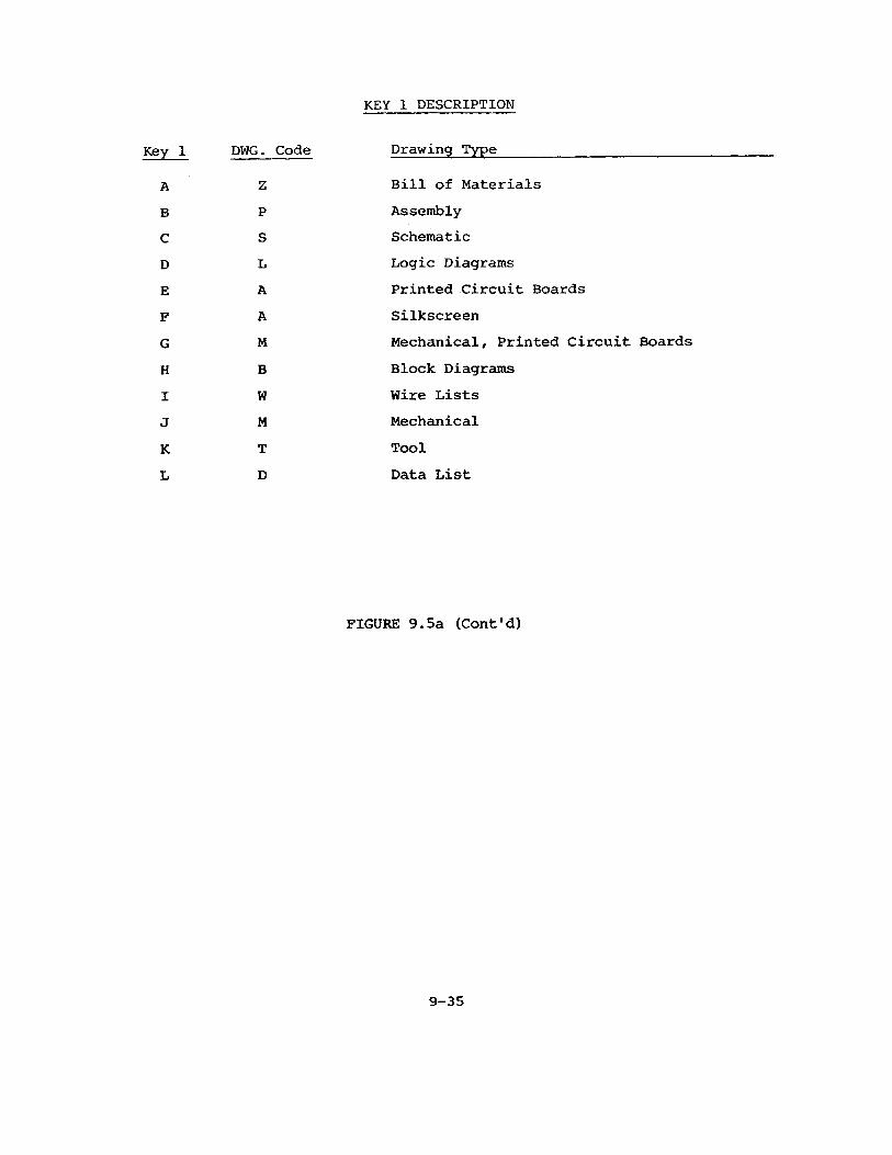
KEY 1 DESCRIPTION
A Z Bill of MaterialsB P AssemblyC S SchematicD L Logic DiagramsE A Printed Circuit BoardsF A SilkscreenG M Mechanical, Printed Circuit BoardsH B Block DiagramsI W Wire Listsj M MechanicalK T ToolL D Data List
FIGURE 9.5a (Cont’d)
Key 1 DWG. Code Drawing Type______________________
9-35
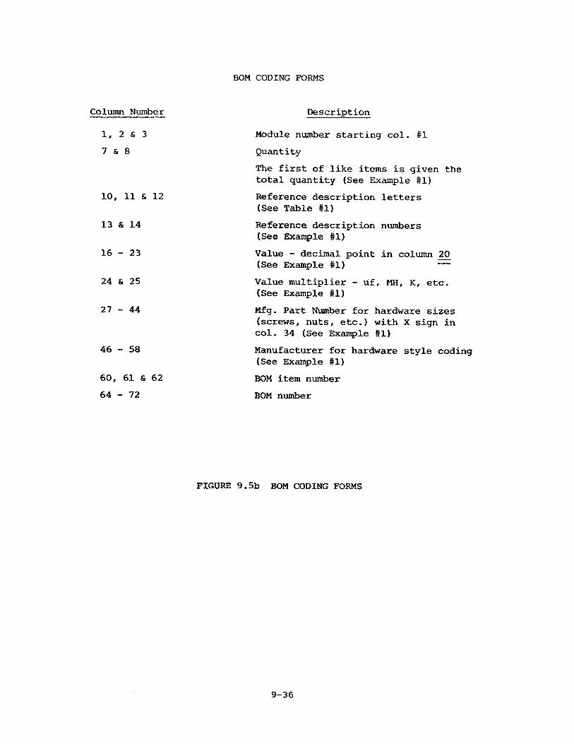
BOM CODING FORMS
1, 2 & 3 7 & 8
1 0, 11 & 12
13 & 14
16 - 23
24 & 25
27 - 44
46 - 58
60, 61 & 62 64 - 72
Column Number
Module number starting col. #1 QuantityThe first of like items is given the total quantity (See Example #1)Reference description letters (See Table #1)Reference description numbers (See Example #1)Value - decimal point in column 20(See Example #1) —Value multiplier - uf, MH, K, etc.(See Example #1)Mfg. Part Number for hardware sizes (screws, nuts, etc.) with X sign in col. 34 (See Example #1)Manufacturer for hardware style coding (See Example #1)BOM item numberBOM number
Description
FIGURE 9.5b BOM CODING FORMS
9-36
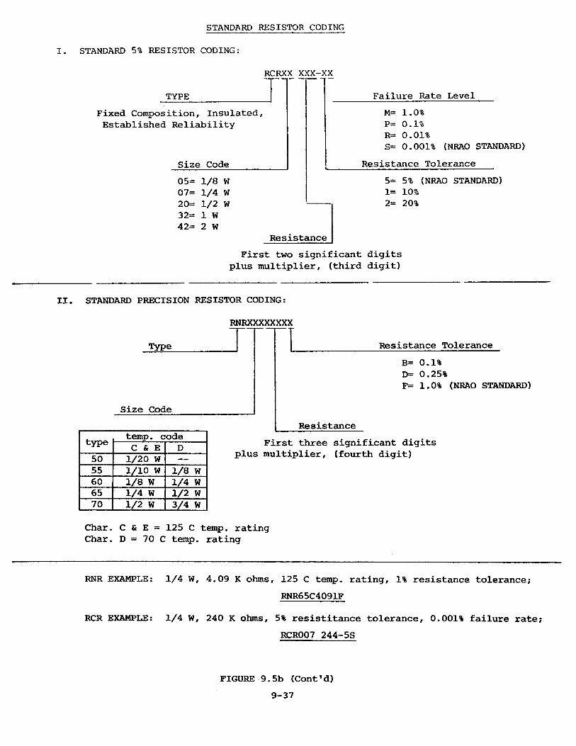
STANDARD RESISTOR CODING
I.
II.
STANDARD 5% RESISTOR CODING:RCRXX X X X -X X
TYPEFixed Composition, Insulated, Established Reliability
Size Code05= 1/8 W 07= 1/4 W 20= 1/2 W
1 W2 W
32=42=
Resistance
Failure Rate LevelM= 1.0%P= 0.1%R= 0.01%S= 0.001% (NRAO STANDARD)
Resistance Tolerance5= 5% (NRAO STANDARD) 1= 10%2= 20%
First two significant digits plus multiplier, (third digit)
STANDARD PRECISION RESISTOR CODING:RNRXXXXXXXX
Type__________
Size Code
type temp. codeC & E D
50 1/20 W —55 1/10 W 1/8 W60 1/8 W 1/4 W65 1/4 W 1/2 W70 1/2 W 3/4 W
Resistance ToleranceB= 0.1%D= 0.25%F= 1.0% (NRAO STANDARD)
ResistanceFirst three significant digits
plus multiplier, (fourth digit)
Char. C & E = 125 C temp, rating Char. D = 70 C temp, rating
RNR EXAMPLE: 1/4 W, 4.09 K ohms, 125 C temp, rating, 1% resistance tolerance;RNR65C4091F
RCR EXAMPLE: 1/4 W, 240 K ohms, 5% resistitance tolerance, 0.001% failure rate;RCR007 244-5S
FIGURE 9.5b (Cont*d) 9-37

PARTS REFERENCE DESIGNATION
A. STANDARD REFERENCE DESIGNATIONSReference designations assigned to parts for B.O.M. coding forms
(lines 10 thru 14) are I.E.E.E. Standard Class Designation Letters unless otherwise specified below.
Example: (R) resistor, (CR) diode, L.E.D., etc. Letter designations are to be listed from line 10 on, with number identifier listed to right. See Fiq. 1.
9 10Lii
1 1ie No
12 13 14 15R 0 2
C R 2 5
Figure 1
B. NON-STANDARD REFERENCE DESIGNATIONS 1. Drawings:
Bill of Materials, (Z)NST - Top Ass'y Bill of Materials NSA - Sub-Ass'y Bill of MaterialsNSB - Sub-Sub Ass'y (2nd Generation) Bill of Materials
Non P.C. Board Assembly Drawings (P)DST - Top Ass'y Drawing DSA - Sub Ass'y DrawingDSB - Sub-Sub Ass'y (2nd Generation) Drawing
Printed Circuit Board Drawings EPCA - Printed Circuit Board Artwork EPCD - Printed Circuit Board Mechanical (Drill Dwg.) EPCP - Printed Circuit Board Assembly Drawings
FIGURE 9.5b (Cont'd)
9-38
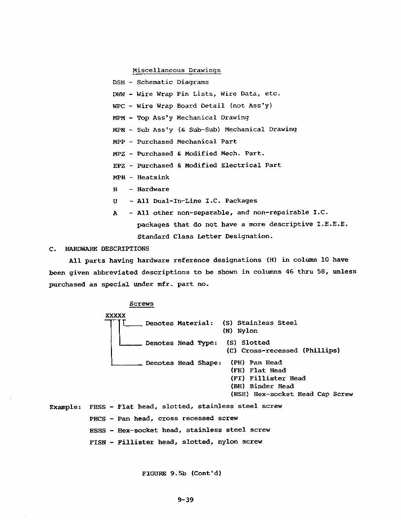
Miscellaneous Drawings DSH - Schematic DiagramsDWW - Wire Wrap Pin Lists, Wire Data, etc.WPC - Wire Wrap Board Detail (not Ass'y)MPM - Top Ass'y Mechanical DrawingMPN - Sub Ass'y (& Sub-Sub) Mechanical DrawingMPP - Purchased Mechanical PartMPZ - Purchased & Modified Mech. Part.EPZ - Purchased & Modified Electrical Part MPH - Heatsink H - HardwareU - All Dual-In-Line I.C. PackagesA - All other non-separable, and non-repairable I.C.
packages that do not have a more descriptive I.E.E.E. Standard Class Letter Designation.
C. HARDWARE DESCRIPTIONSAll parts having hardware reference designations (H) in column 10 have
been given abbreviated descriptions to be shown in columns 46 thru 58, unless purchased as special under mfr. part no.
ScrewsXXXXX
T Denotes Material:
Denotes Head Type:
Denotes Head Shape:
(S) Stainless Steel (N) Nylon(S) Slotted(C) Cross-recessed (Phillips)(PH) Pan Head(FH) Flat Head(FI) Fillister Head (BH) Binder Head(HSH) Hex-socket Head Cap Screw
Example: FHSS - Flat head, slotted, stainless steel screw PHCS - Pan head, cross recessed screw HSHS - Hex-socket head, stainless steel screw FISN - Fillister head, slotted, nylon screw
FIGURE 9.5b (Cont'd)
9-39

Washers and Nuts HNS - Hex Nut, Stainless Steel HNN - Hex Nut, Nylon FWS - Flat Washer, Stainless Steel FWN - Flat Washer, NylonSLWS - Split-lock Washer, Stainless Steel.ITLWS - Internal-tooth Lock Washer, Stainless Steel
FIGURE 9.5b (Cont'd)

i-41
juuuimwu lZKwr / ' / w
iU ltW tN TNUM IU
FORTRAN STATEMENT
vo
i } 3 * i’ A O o^d-vd co«d IW
m
fei&
h i
M
. A
10 II 12 11 14
!ec
— - to
jc 1 §few I!w Jw iHLIL_Mwit p!ca >
SPC.P; ■E PCP ■
M5Ti1
S£A l
HR 3;5R _
11
m
16 17 i i
/i» 20
f21 72
<#>23 24 25
K.KI $ d
%$
0
f iCPi.u£
9
2<6f KI f f •
. 4 -
27 78 79 30idd/Jy
31 :z’
12 33 34 35 3Ms-
6 37 36 39 41-isa
a 4i 4rnr“ 1J
/?|c/ s i :3?
2.. i f be i
P3:f i
•as?|5J
\3__- j LAsS
m ■31 ISi5«fc i LL - § 1M 1v |sMis s 4s<’ >pSi55 I ] P X: jI - • 4 gNuSi*>
UM -' “ 6 ■zSi
r—i-?H f _&”13'2 )B i :3|2 3'< 212T tffi32 3'lJABd?fkL 32 3- p ia i .31 3.IiM11Aj i i 3 m 56D!.32 ppm i417 " i | -2 ^ 4 -• J”
R5 ?2tf0:ZF\RCc±z:g 5 4)1'■ 5|?
p«?_ 1_L-1—i
J14 1 : all hdwrg
6&CIMAL POlMTS LIMB 32: LEAVB SPACE: BEnV&fiN/
size 4 valus cooes on srv.5 % R6SI&TORS
I—Liwe Z7J ALL HDWR& COPS -L ine 2o: ALL P6CIMAL POINTS VOR COMPONEKfTS
R6C?UiejMS VALU6S.NOTB: ALL identical PARTS Wi t h Muir/pie QOAbmnes, p u t to ta l on?
WITH FIRST ITBM ONLY,
NO MFfc NEE PSP I FOR ST'Ct RSSIS
• • N u m b e r ol lo rm i p « r p » d m a y v io r »Mgniiy
FIGURE 9.5b (Cont'd)
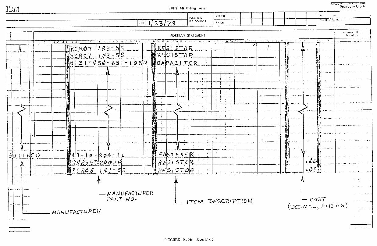
L)/>LJU - / u / m iJ-i.
P U N C H IN G
I N S 1RUC H O N S
C k A H llC * - • . t W l
1/23/7/? PU N C H
• •' M ) I I t V- 1 Ki-J 1 l U / . ’.l-l •
FIGURE 9.5b (Cont'c’)

9.6 Standard AMP Connector Components and ToolsTable 9.6a and 9.6b are a collection of the AMP hardware
which has been selected for use in VLA.
9-43
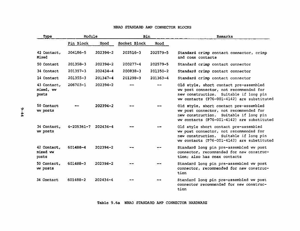
9-44
NRAO STANDARD AMP CONNECTOR BLOCKS
JSBBS.
42 Contact, Mixed50 Contact 34 Contact 14 Contact43 Contact, mixed, ww posts
50 Contact ww posts
Module BinPin Block Hood
204186-5
201358-3201357-3201355-3206703-1
202394-2
202394-2202434-4201347-4202394-2
202394-2
34 Contact, 4-205361-7 202434-4 ww posts
42 Contact, 601488-4 202394-2mixed wwposts50 Contact, 601488-3 202394-2 ww posts
34 Contact 601488-2 202434-4
Socket Block Hood
202516-3 202579-5
200277-4 202579-5 200838-3 201350-2 201298-3 201363-4
Remarks
Standard crimp contact connector, crimp and coax contactsStandard crimp contact connectorStandard crimp contact connectorStandard crimp contact connectorOld style, short contact pre-assembled ww post connector, not recommended for new construction. Suitable if long pin ww contacts (P76-001-4142) are substitutedOld style, short contact pre-assembled ww post connector, not recommended for new construction. Suitable if long pin ww contacts (P76-001-4142) are substitutedOld style short contact pre-assembled ww post connector, not recommended for new construction. Suitable if long pin ww contacts (P76-001-4142) are substitutedStandard long pin pre-assembled ww post connector, recommended for new construction; also has coax contactsStandard long pin pre-assembled ww post connector, recommended for new constructionStandard long pin pre-assembled ww post connector recommended for new construction
Table 9.6a NRAO STANDARD AMP CONNECTOR HARDWARE

9-45
CONNECTOR HARDWARE
42/50 Block Strain relief, long - 201847-■1
42/50 Block Shield and cable clamp, 180° short,
34 Block Strain relief, long - 201846--1
34 Block Shield and cable clamp, 180° short,
Fixed male jackscrews - 200844-2
Turnable female jackscrews - 206867-2
STANDARD AMP CONNECTOR POWER PIN ASSIGNMENTS
Type tolor Code
+5 Logic Orange
Logic Common Black
+15 V Red
-15 V Yellow
+20 V Blue
+28 V Gray
-28 V Dark Green
-5.2 V Brown
Hi-Q Gnd Black
117 V AC Hot Black/White
117 v ; Whit
42 mixed 10 34 16 17 28 29 11 42 33 41
50 C L,B A E D F J H HH N/A M/A
34 N/A N/A N/A N/A N/A N/A N/A N/A N/A N/A N/A
14 C B E — A P R D N/A N/A
Table 9.6a Cont'd
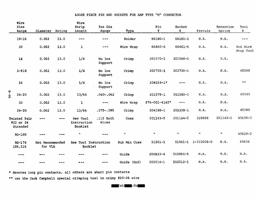
9-46
LOOSE PIECE PIN AND SOCKETS FOR AMP TYPE "M" CONNECTOR
WireSizeRange Diameter Rating
WireStripLength
Ins Dia Range Type
Pin#
Socket# Ferrule
Retention Tool Spring______#
18-16
30
14
2-#18
16
24-20
30
24-20
Twisted Pair #22 or 24 Stranded
RG-188
RG-174188,316
0.062
0.062
0.062
0.062
0.062
0.062
0.062
0.062
13.0
13.0
13.0
13.0
13.0
13.0
13.0
13.0
Not Recommended for VLA
1/4
1/4
1/4
13/64
1
13/64
See Tool Instruction Booklet
No Ins Support
No Ins Support
No Ins Support
.040-.062
,075-.085
115 Both Wires
See Tool Instruction Booklet
Solder Wire Wrap
Crimp
Crimp
Crimp
Crimp Wire Wrap
Crimp
Coax
Sub Min Coax
66180-1
66460-6
201570-1
66181-1
66461-6
201568-1
202725-1 202726-1
204219-1* ---
201578-1 201580-1 P76-001-4142*
204188-1 201328-1
201143-5 201144-5
51561-1
N. A.
N . A.
N . A.
N. A.
N. A.
N.A.N . A.
N.A.
328666
Guide 200833-4 203964-6 N.A.
Guide (Gnd) 202514-1 202512-1 N.A.
* denotes long pin contacts, all others are short pin contacts** use the Jack Campbell special crimping tool to crimp #20-26 wire
■■PabflM. 6bB
N.A.
N.A.
N.A.
N.A.
N.A.
N.A.N.A.N.A.
201142-2
51561-1 1-332056-0 N.A,
N.A,N.A,
Std Wir6 Wrao Tool
45098
45099
45099
45638-3
45628-2
69656
N.A.
N.A.
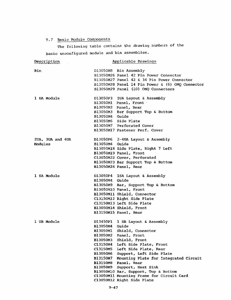
9.7 Basic Module ComponentsThe following table contains the drawing numbers of the
basic unconfigured module and bin assemblies.Description
Bin
1 UA Module
2UA, 3UA and Modules
1 SA Module
1 UB Module
Applicable Drawings
D13050M8 Bin Assembly B13050M26 Panel 42 Pin Power Connector B13050M27 Panel 42 & 34 Pin Power Connector B13050M28 Panel 14 Pin Power & (6) OMQ Connector B13050M29 Panel (10) OMO Connectors
D13050P3 IUA Layout & AssemblyB13050M1 Panel, FrontB13050M2 Panel, RearB13050M3 Bar Support Top & BottomB13050M4 GuideB13050M6 Side PlateB1305QM7 Perforated Cover B13050M17 Fastener Perf. Cover
4UA D13050P6 2-4UA Layout & AssemblyB13050M4 GuideB13050M18 Side Plate, Right 7 Left B13050M19 Panel, Front C13050M22 Cover, Perforated B13050M23 Bar Support Top & Bottom B13050M24 Panel, RearD13050P4 ISA Layout & Assembly B13050M4 GuideB13050M9 Bar, Support Top & Bottom B13050M10 Panel, Front B13050M11 Shield, Connector C13150M12 Right Side Plate C13150M13 Left Side Plate B13050M14 Shield, Front B13150M15 Panel, RearD13450P1 1 SB Layout & AssemblyB13050M4 GuideB13050M1 Shield, ConnectorB13050M2 Panel, FrontB13050M3 Shield, FrontC13150M4 Left Side Plate, FrontC13150M5 Left Side Plate, RearB13050M6 Support, Left Side PlateB13150M7 Mounting Plate for Integrated CircuitB13150M8 Panel, RearB13050M9 Support, Heat SinkB13050M10 Bar, Support, Top & BottomC13050M11 Mounting Frame for Circuit CardC13050M12 Right Side Plate
9-47
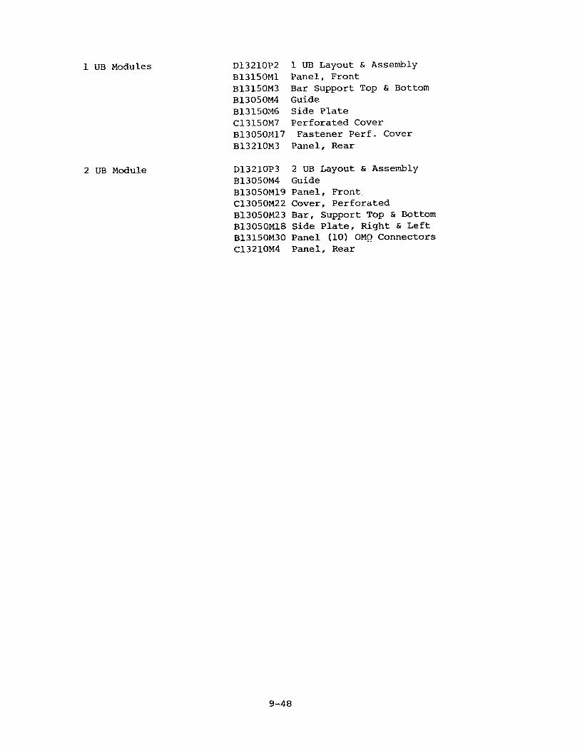
1 UB Modules D1321QP2 1 UB Layout & AssemblyB13150M1 Panel, FrontB13150M3 Bar Support Top & BottomB13050M4 GuideB13150M6 Side PlateC13150M7 Perforated CoverB13050M17 Fastener Perf. CoverB13210M3 Panel, Rear
2 UB Module D13210P3 2 UB Layout & AssemblyB13050M4 Guide B13050M19 Panel, Front C13050M22 Cover, Perforated B13050M23 Bar# Support Top & Bottom B1305QM18 Side Plate, Right & Left B13150M30 Panel (10) 0M0 Connectors C13210M4 Panel, Rear
9-48
9.8 Graphic Electrical, Electronic and Logic SymbolsIEEE Standard #315 Mar 1971 shall be used for graphic elec
trical and electronic symbols. American National Standard Institute ANSI Y32.14-1973 shall be used for graphic digital logic symbols.
9.9 Dimensioning and TolerancingANSI Y1-.5-1973 shall be the applicable specification for
dimensioning and tolerancing.
9.10 Miscellaneous Specifications1) Mil Std 12c - Military Standard Abbreviations for use
on drawings Specifications and Technical Documents
2) Federal Standard 595a, Color Chips for Desk Use
3) IEEE Recommended abbreviations, extracted from the publication "Information for IEEE Authors."
9-49

I. Recommended prefixesMultiple Prefix Symbol
10'* tera T10» g'ga G10* mega M10a kilo k10= hecto hia deka daio-» deer d10-* cent! cio-» milli m10"* micro pio-» nano nio -« pico P1 0 * femto f10-» atto a
Factor by Which the Unit Is Multiplied Prefix
Symbol
1000000000000 =» 10l* tera T1 000 000 000 - 10* giga G
1 000 000 =* 10‘ mega M1 000 -• 103 kilo k
100 = 10* hecto h10 - 10l dekaj da
0.1 - 10-‘ deci d0.01 - 10-* centi c
0.001 = 10-J milli m0.000001 - 10-* micro
0.000000001 =■ 10-* nano n0.000 000 000 001 « 10"1* pico P
0.000 000000 000001 - 10“ls femto § f.000000000 000000001 - 10-“ atto§ a
9-50
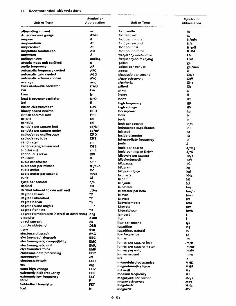
II. Recommended abbreviations
Symbol or Symbol orUnit or Term Abbreviation Unit or Term Abbreviation
alternating current acAmerican wire gauge AWGampere Aampere-hour Ahampere-turn Atamplitude modulation AMangstrom Aantilogarithm antilogatomic mass unit (unified) uaudio frequency AFautomatic frequency control AFCautomatic gain control AGC-automatic volume control AVCaverage avgbackward-wave oscillator BWObar barbarn bbeat-frequency oscillator BFObel Bbillion electronvolts* BeVbinary coded decimal BCDBritish thermal unit Btucalorie calcandela cdcandela per square foot cd/ft*candela per square meter cd/m*cathode-ray oscilloscope CROcathode-ray tube CRTcentimeter cmcentimeter-gram-second CGScircular mil cmilcontinuous wave CWcoulomb Ccubic centimeter cm3cubic foot per minute ft3/mincubic meter m*cubic meter per second m*/scurie Cicycle per second c/sdecibel dBdecibel referred to one milliwatt dBmdegree Celsius *Cdegree Fahrenheit *Fdegree Kelvin #Kdegree (plane angle) . . .*degree Rankine *R degree (temperature interval or difference) degdiameter diamdirect current dcdouble sideband DSBdyne dynelectrocardiograph EKGelectroencephalograph EEGelectromagnetic compatibility EMCelectromagnetic unit EMUelectromotive force EMFelectronic data processing EDPelectronvolt eVelectrostatic unit ESUerg ergextra-high voltage EHVextremely high frequency EHFextremely low frequency ELFfdrad Ffield-effect transistor FETfoot ft
footcandle fcfootlambert fLfoot per minute ft/minfoot per second ft/sfoot poundal ft*pdlfoot pound-force ft-lb ffrequency modulation FMfrequency-shift keying FSKgallon galgallon per minute gal/mingauss Ggigacycle per second Gc/sgigaelectronvolt GeVgigahertz GHzgilbert Gbgram ghenry Hhertz Hzhigh frequency HFhigh voltage HVhorsepower hphour hinch ininch per second in/sinductance-capacitance LCinfrared IRinside diameter IDintermediate freauency IFjoule Jjoule per degree J/degjoule per degree Kelvin J/*Kkilocycle per second kc/skiloelectronvolt keVkilogauss kGkilogram kgkilogram-force kgfkilohertz kHzkilohm knkilojoule kJkilometer kmkilometer per hour km/hkilovar kvarkilovolt kVkilovoltampere kVAkilowatt kWkilowatthour kWhlambert Lliter 1liter per second I/slogarithm loglogarithm, natural Inlow frequency LFlumen Imlumen per square foot lm /ft!lumen per square meter lm /m 5lumen per watt Im/Wlumen second lm-slux Ixmagnetohydrodynamics MHDmagnetomotive force MMFmaxwell Mxmedium frequency MFmegacycle per second Mc/smegaelectron volt MeVmegahertz MHzmegavolt MV
9-51

Unit or TermSym bol or
Abbreviation U n it or T ermSymbol or
Abbreviation
megawatt MVVmegohm Mrtmet3i-oxid« semiconductor MOSmeter mmeter-kilogram-second MKSmho mhoI’nlcroampere pAmicrofarad *Fmicrogram **gmicrohenry pHmicrometer pmmicromho /imhomicron f **microsecond MSmicrosiemens /iSmicrowatt /*Wm il milmile per hour m i/hmile (statute) mimilliampere mAmilligram mgmillihenry mHmilliliter mlmillimeter mmmillimeter o f mercury, conventional millimicron J
mmHg
millisecond msmillisiemens m Smillivolt mVmilliwatt mWminute (plane angle> *minute (tim e) m»i>nanoampere nAnanofarad nFnanometer nmnanosecond nsnanowatt nWnautical mile nmineper Npnewton Nnewton meter N -mnewton per square meter N /m 1oersted Oeohm oounce(avoirdupois) ozoutside diameter ODphase modulation PMpicoampere pApicofarad PFpicosecond PSpicowatt pWpound lbpoundal pdlpound-force Ibfpound-force foot Ib f-ftpound-force per square inch lbf/in*pound per square inch§ psipower factor PFprivate branch exchange P8Xpulse-ampfitude modulation PAMpulse-code modulation PCMpulse-count modulation PCMpulse-duration modulation PDMpulse-position modulation PPMpulse-repetitkm frequency PRF
pulse-repetition rate PRRpulse-time modulation PTMpulse-width modulation PWMradian radradio frequency RFradio-frequency interference RFtresistance-capacitance RCresistance-inductance-capacitance RLCrevolution per minute r/rninrevolution per second r/sroentgen Rroot-mean-square rmssecond (plane angle) *second (time) sshort wave swsiemens ssignal-to-noise ratio SNRsilicon controlled rectifier SCRsingle sideband SSBsquare foot ft*square inch in*square meter m*square yard yd*standing-wave ratio SWRsteradian srsuperhigh frequency SHFtelevision TVtelevision interference TVItesla Tthin-film transistor TFTtransverse electric TEtransverse electromagnetic TEMtransverse magnetic. TMtraveling-wave tube TWTultra high frequency UHFultraviolet UVvacuum-tube voltmeter VTVMvar varvariable-frequency oscillator VFOvery-high frequency VHFvery-low frequency VLFvestigia) sideband VSBvolt Vvoltage controlled oscillator VCOvoltage standing-wave ratio VSWRvoltampere VAvolume unit vuwatt Wwatthour Whwatt per steradian W/srwatt per steradian square meter W/Csr-m5)weber Wbyard yd
* Deprecated; use glgaelectronvoU (GeV). f The name micrometer (pm) Is preferred.$ The name nanometer is preferred.{ Although the use of the nbbreviation pst is common. It is not recommended. See pound-force per square inch.
R eprin ts o f these instructions a rc available on request from the Editorial .D epartm ent, Institu te o f Electrical and Electronics Engineers, Inc., 345 East 47ih S treet, New York, N .Y. 10017.
9-52