Embed Size (px)
Citation preview
VHDL IMPLEMENTATION OF A HIGH-SPEED SYMMETRIC
CROSSBAR SWITCH
by
Maryam Keyvani
B.Sc., University of Tehran, 1998
THESIS SUBMITTED IN PARTIAL FULFILLMENT OF
THE REQUIREMENTS FOR THE DEGREE OF
MASTER OF APPLIED SCIENCE
in the School
of
Engineering Science
© Maryam Keyvani 2001
SIMON FRASER UNIVERSITY
August 2001
All rights reserved. This work may not be
reproduced in whole or in part, by photocopy or other means, without permission of the author.
ii
Approval
Name: Maryam Keyvani
Degree: Master of Applied Science
Title of thesis: VHDL implementation of a high-speed symmetric
crossbar switch.
Examining Committee:
Dr. Mehrdad Saif
Chair
Dr. Ljiljana Trajkovic Senior Supervisor
Dr. Stephen Hardy Supervisor
Dr. Tony Dixon Examiner School of Computer Science Simon Fraser University
Date Approved:
iii
Abstract
We describe the methodology, the design, and the VHDL
implementation of three main blocks of a 4×4 input buffered crossbar
switch: the input port modules, the crossbar scheduler module, and the
crossbar fabric module. The components employ existing schemes and
architectures. However, the design and VHDL implementation of each of
the components, and the composition of the overall switch is a novelty.
All the blocks are implemented in VHDL employing an ALTERA
FLEX10KE device and using MAX+PLUS II software. The switch is
capable of handling asynchronous transfer mode (ATM) packets.
ATM packets enter the input data lines of the switch in the form of
bytes. Every input port module of the switch has a corresponding input
buffer. The data bytes entering the switch are first stored in this buffer.
There are four “dynamic virtual input queues” within each of the input
buffers. Based on the output port that the packet is destined for, every
packet in the input buffer is assigned to one of these four virtual queues.
The destination output port of every packet is determined based on the
Virtual Circuit Identifier (VCI) information from the header of the packet.
This VCI value is looked up in a routing table to determine the
destination output port and the updated VCI for the packet. A request
for the destination output port is then sent to the scheduler module of
the switch. The crossbar scheduler employs a round robin priority
rotation scheme that is fair to all the input ports. The scheduler
configures the fabric, and grants the requests of some or all the input
ports based on their position in the priority round robin. Any input port
iv
that receives a grant de-queues the packet from its input buffer and
sends it to the crossbar fabric module, which provides the physical
connection between the input and the output ports.

v
Acknowledgements
I would like to thank my senior supervisor, Dr. Ljiljana Trajkovic, for her
support, encouragement and guidance during the period of my studies.
She taught me a lot about research and guided me through every step of
my studies. I would also like to thank my co-supervisor, Dr. Stephen
Hardy, for his kindness, support, guidance, and valuable comments.
I would like to extend my special thanks to my friend and colleague
Arash Haidari. We started this project together and he was my partner in
designing the Fabric and the Scheduler modules. Without him this
project would not have gone forward. I thank him for his moral and
technical support.
My sincere thanks to Dr. Tony Dixon for his willingness to be in my
defense committee and his valuable comments.
Special thanks to my family for their support and kindness. Sincere
thanks to all my friends, specially Nazy Alborz, for their friendship and
support throughout the period of my studies at SFU.
vi
Table of Contents
Approval ............................................................................................. ii
Abstract.............................................................................................. iii
Acknowledgments ..............................................................................v
List of Figures .................................................................................... ix
List of Tables ......................................................................................xi
1. Introduction ...................................................................................1
2. Background information ................................................................7
2.1. Internal interconnect of the switch....................................7
2.1.1. Bus architecture ...................................................7
2.1.2. Ring architecture ..................................................9
2.1.3. Crossbar architecture ...........................................10
2.1.4. Multistage architecture .........................................11
2.2. Buffering in packet switches .............................................13
2.2.1 Output queues.......................................................13
2.2.2. Shared central buffers ..........................................14
2.2.3. Input queues.........................................................14
2.3. Scheduling algorithms ......................................................22
3.3. Examples of existing ATM switches ...................................27
3. High-level switch view ....................................................................30
4. Input ports .....................................................................................34
4.1. Input buffer .......................................................................36
4.2. Counters............................................................................41
4.3. Look-up table (port_LUT) ...................................................42
4.4. VCI registers ......................................................................43
4.5. Write sequence controller (Write_seq_SM state machine)..44
vii
4.6. VCI controller (VCI_SM state machine)..............................46
4.7. Read sequence controller (Read_seq_SM state machine) ..48
4.8. Linked list update controller (linked_list_update process) 51
4.8.1. Initializing the linked lists ....................................51
4.8.2. Updating linked lists after a packet has been
written ............................................................................52
4.8.3. Updating the linked lists after a packet has been
read.................................................................................55
5. The scheduler ................................................................................58
5.1. Two dimensional ripple-carry arbiter.................................59
5.2. Diagonal propagation arbiter (DPA) architecture ...............62
6. The fabric .......................................................................................69
7. Device information and simulation results.....................................76
7.1. Device information.............................................................76
7.2. Simulation results .............................................................78
7.2.1. Simulation results of the switch (Appendix D.1)...78
7.2.2. Simulation results of the input port module
(Appendix D.2) ................................................................82
Conclusion and future work...............................................................83
References .........................................................................................86
Appendix A. Detailed schematic of the switch with its internal
connections........................................................................................91
Appendix B. Sample output port module...........................................92
Appendix C. VHDL source code of the switch and its components ....95
Appendix C.1. voq_switch.vhd...................................................96
Appendix C.2. voq_input.vhd....................................................106
Appendix C.3. voq_c_bar.vhd ....................................................123
viii
Appendix C.4. voq_fabric.vhd....................................................131
Appendix C.5. LUT.vhd.............................................................137
Appendix C.6. output_fifo.vhd ..................................................141
Appendix C.7. voq_input_package.vhd......................................151
Appendix D. Simulation results .........................................................153
Appendix D.1. Simulation results for the voq_switch project....154
Appendix D.2. Simulation results for the voq_input project .....145
ix
List of Figures
Figure 2.1: Schematic of a bus architecture switch............................8
Figure 2.2: Schematic of a ring architecture switch ...........................9
Figure 2.3: An input buffered switch with crossbar architecture .......10
Figure 2.4: An 8×8 Omega architecture .............................................12
Figure 2.5: A 4×4 three-stage Clos architecture.................................12
Figure 2.6: An input buffered switch with periodic traffic..................16
Figure 2.7: Simple virtual output queuing (VOQ) structure ...............17
Figure 2.8: Alternative designs of switches with input port buffers....19
Figure 2.9: Input port queues for K-HOL scheme ..............................21
Figure 2.10: Bipartite graph G, and a matching W on it ....................22
Figure 2.11: Round robin matching (RRM) scheduling algorithm .....26
Figure 3.1: High-level schematic of the switch ...................................31
Figure 4.1: High-level schematic of voq_input module of the switch ..34
Figure 4.2: (a) An ATM cell consisting of a 5 byte header and a 48 byte
payload. (b) The User Network Interface (UNI) ATM cell header..........35
Figure 4.3: Voq_input module data path............................................38
Figure 4.4: The structure of the buffer in each voq_input module .....39
Figure 4.5: The port_LUT component.................................................43
Figure 4.6.a: Write sequence state machine in each input port
module ...............................................................................................44
Figure 4.6.b: Reset check in write sequence state machine...............45
Figure 4.7: VCI state machine in each input port module .................47
Figure 4.8.a: Read sequence state machine in each input port
module ...............................................................................................48
Figure 4.8.b: Reset/grant check in read sequence state machine .....49
x
Figure 4.9: The initial state of the ready flags and the next registers
associated with each block of the buffer.............................................51
Figure 4.10: Diagram of the steps taken within the linked list update
process to update the linked lists, the next registers, and the ready
flags after a packet is written in the input buffer...............................53
Figure 4.11: Diagram of the steps taken within the linked list update
process to update the linked lists, the next registers, and the ready
flags after a packet is de-queued from the input buffer .....................55
Figure 5.1: Two dimensional ripple-carry arbiter ...............................59
Figure 5.2: The basic arbiter cell with the combination logic
inside it ..............................................................................................60
Figure 5.3: Fixed priority Diagonal Propagation Arbiter (DPA)...........63
Figure 5.4: Diagonal Propagation Arbiter (DPA) .................................66
Figure 5.5: Modified arbitration cell for diagonal propagation arbiter
(DPA) architecture ..............................................................................67
Figure 5.6: Diagonal Propagation Arbiter (DPA) .................................67
Figure 6.1: Crossbar fabric module in our switch ..............................69
Figure 6.2: A 4×4 crossbar .................................................................71
Figure 6.3: Crossbar for the voq_fabric module ..................................71
Figure 6.4: The output_fp(2) is the logical sum of input_fp bits 72
AND’d with corresponding cntrl bits.
Figure 6.4: The 12 copies of crossbar used in the voq_fabric module.73
Figure 6.5: The crossbar used to pass the data_valid signals through
the fabric...........................................................................................74
Figure 6.6: The crossbar used to pass the 3rd bit of the data bytes
through the fabric..............................................................................75
xi
List of Tables
Table 7.1: Summery of the gates and logic cells used for the crossbar
switch.................................................................................................76
Table 7.2: The input VCI, output VCI, and output port numbers
stored in the look up table module of our switch ...............................79
Table 7.3: Details of simulation results shown in Appendix D.1........81
1
Chapter 1
Introduction
Communication networks connect different geographically distributed
points, so that these points can communicate with each other. Since a
completely connected graph of such a network with N points would
require N(N-1)/2 links -practical for only small N- a partially connected
network is typically used.
Switching refers to the means by which the transmission facilities
(bandwidth, buffer capacity, etc.) are allocated to users to provide them
with a certain degree of connectivity. Switching systems reduce the
overall network costs by reducing the number of transmission links
required to enable a given population of users to communicate. They
also enable heterogeneity among terminals and transmission links, by
providing a variety of interface types. According to the type of
information being carried, there are various switching techniques,
chosen on the basis of optimizing the usage of bandwidth in the
network. The two main switching techniques are: circuit switching and
packet switching.
In circuit switching, a path is set up from the source to the destination
at the connection set-up time. Once this path is set up, it remains fully
connected for the duration of the connection. It is obvious that circuit
switching is only cost effective at times when there is a continuous flow
of data once the circuit is set up. This is certainly the characteristic of
2
voice communication and that is why circuit switching is mostly used in
telephone networks.
Communication among computers however, happens in bursts. Data
travels through these networks in the form of messages. Each message is
a block of data with a header that contains some control information
such as source and destination addresses, priority, message type, etc. In
data networks, there are certain gaps between the messages. The user
devices do not need the transmission link all the time, but when they
do, they require relatively high bandwidths. Assigning a continuous
connection with high bandwidth for such connections is obviously a
waste of resources and results in low utilizations. If the circuit of high
bandwidth was set up and released for each message transmission, then
the set up time incurred for each message transmission would be high
compared to the transmission time of the message. Thus, switches in
data networks incorporate the store and forward technique for
transmitting the messages.
In store and forward, a message is first sent from the source to the
switch to which it is attached. The switch scans the header of the
message and decides to which output to forward the message. The same
scheme is repeated from switch to switch until the message reaches its
destination. The advantage of such a switching scheme is that the
transmission links are occupied only for the duration of the
transmission of a message. After that the links are released in order to
transmit other messages. In other words, the bandwidth allocation in the
3
store and forward scheme is determined dynamically on the basis of a
particular message and a particular link in the network.
Packet switching is an extension of message switching. In packet
switching, messages are broken into certain blocks called packets, and
packets are transmitted independently using the store and forward
scheme. Some of the advantages of packet switching over message
switching according to [24] are as follows.
1) Messages are fragmented into packets that cannot exceed a
maximum size. This leads to fairness in the network utilization,
even when messages are long.
2) Successive packets in a message can be transmitted
simultaneously on different links, reducing the end-to-end
transmission delay. (This effect is called pipelining.)
3) Due to the smaller size of packets compared to messages, packets
are less likely to be rejected at the intermediate nodes due to
storage capacity limitation at the switches.
4) Both the probability of error and the error recovery time will be
lower for packets since they are smaller. Once an error occurs,
only the packet with the error needs to be retransmitted rather
than the whole message. This leads to a more efficient use of the
transmission bandwidth.
A packet switch is a box with N inputs and N outputs that routes the
packets arriving on its inputs to their requested outputs. One can say
that the main functions of packet switches are buffering and routing.
4
Besides these basic operations a switch can have other capabilities, such
as handling multicast traffic and priority functions.
Small N×N packet switches are the key components of the
interconnection networks used in multiprocessors and integrated
communication networking for data, voice, and video. A popular choice
in the hardware implementation of packet switches is crossbar
architecture [5, 13, 18, 22, 26]. Crossbar is a non-blocking architecture.
This means that any input-output pair can communicate with each other
as long as they do not interfere with the other input-output pairs. In
other words, any permutation of inputs and outputs is possible as long
as each input sends data to a different output, and each output receives
data from at most one input.
This document describes the design and implementation of an
asynchronous transfer mode (ATM) crossbar switch [14]. ATM is a means
of digital communication with the potential for replacing the conflicting
communication infrastructures (telephone networks, cable TV networks,
and computer networks) that nowadays need to be integrated into one.
These three information infrastructures have some overlaps among
themselves and are all moving from analog technology to digital
technology for transmission, switching, and multiplexing. New
technologies are being developed that are stepping along the way of
merging these three communication infrastructures. ATM technology is
intended to be used in networks that transport a variety of different
types of information including voice traffic that was traditionally carried
over telephone networks, data traffic typically carried on computer
5
networks, and multimedia traffic consisting of a mixture of image, audio
and video information. Each of these various types of traffic can have a
different requirement and places different demands on switching and
transmission facilities. Although ATM has not replaced datagram
networks altogether and hasn’t been the one and only dominant
technology (as it was promising 10 years ago), but still it has been
deployed in many networks. Vendors are continuing to study and
improve ATM technology to achieve the implementation of more and
more Quality of Service (QoS). In ATM networks data is transferred over
Virtual Circuits (VC’s) in 53-byte packets called cells.
Our implementation is done in VHSIC Hardware Description Language
(VHDL), using MAX+PLUS II software. The ATM crossbar switch that we
have implemented is a modular design (can be scaled) and consists of
three main components: input port modules, crossbar scheduler, and
crossbar fabric. The functionality of the switch can be described as
follows. The packets first enter the input ports of the switch where they
are queued based on their order of arrival. Each input port has a port
controller that determines the destination of a packet, based on the
packet header using a programmable mapper (routing table). The port
controller then sends a request to the scheduler for the destination
output port. The scheduler grants a request based on a priority
algorithm that ensures fair service to all the input ports. Once a grant is
issued, the crossbar fabric is configured to map the granted input ports
to their destination output ports.
6
Chapter 2 provides background information on queuing schemes, fabric
architectures and designs, and scheduling algorithms in packet
switches. We also introduce several examples of existing ATM switches.
In Chapter 3 an overall view of our switch is presented. Chapter 4
contains a detailed description of the switch input port modules. The
crossbar scheduler and crossbar fabric modules are introduced in
Chapters 5 and 6, respectively. Finally, Chapter 7 discusses the
implementation details and the simulation results of our design.
There are four Appendices in this document. Appendix A contains a
detailed schematic of our 4×4 packet switch and its internal
connections. Appendix B has the description of a sample output port
module that can be connected to the output ports of the switch.
Appendices C and D contain the source code for all the components and
the simulation results from the design, respectively.
7
Chapter 2
Background information
There are three main components in packet switches: 1) the block that
provides the physical connection between the input and output ports
(internal interconnect of the switch), 2) the internal storage (memory, in
general) where the packets that enter the switch are stored, and 3) the
scheduling module that determines the departure of packets from the
switch.
This Chapter provides background information on different designs,
architectures, and algorithms for these main components of packet
switches. In each case, the pros and cons of the architectures or
algorithms are discussed.
2.1. Internal interconnect of the switch
There have been discussions about what the internal interconnect of the
switch should be [3, 25]. The internal interconnect of the switch can be
in the form of a single stage network (shared bus, ring, crossbar) or a
multi-stage network of smaller switches arranged in a banyan [9]. What
follows are some pros and cons of each of these schemes.
2.1.1. Bus architecture
Bus architecture is probably the simplest way of transferring data to the
output ports (Figure 2.1). The inputs and outputs of the switch are
connected to a single bus or a number of parallel buses. The inputs have
to contend for the control of the bus. A bus arbitration technique has to
8
be implemented in the bus processor to arbitrate the control of the bus
among the input ports. In bus architecture switches, queuing is mostly
done at the output ports of the switch.
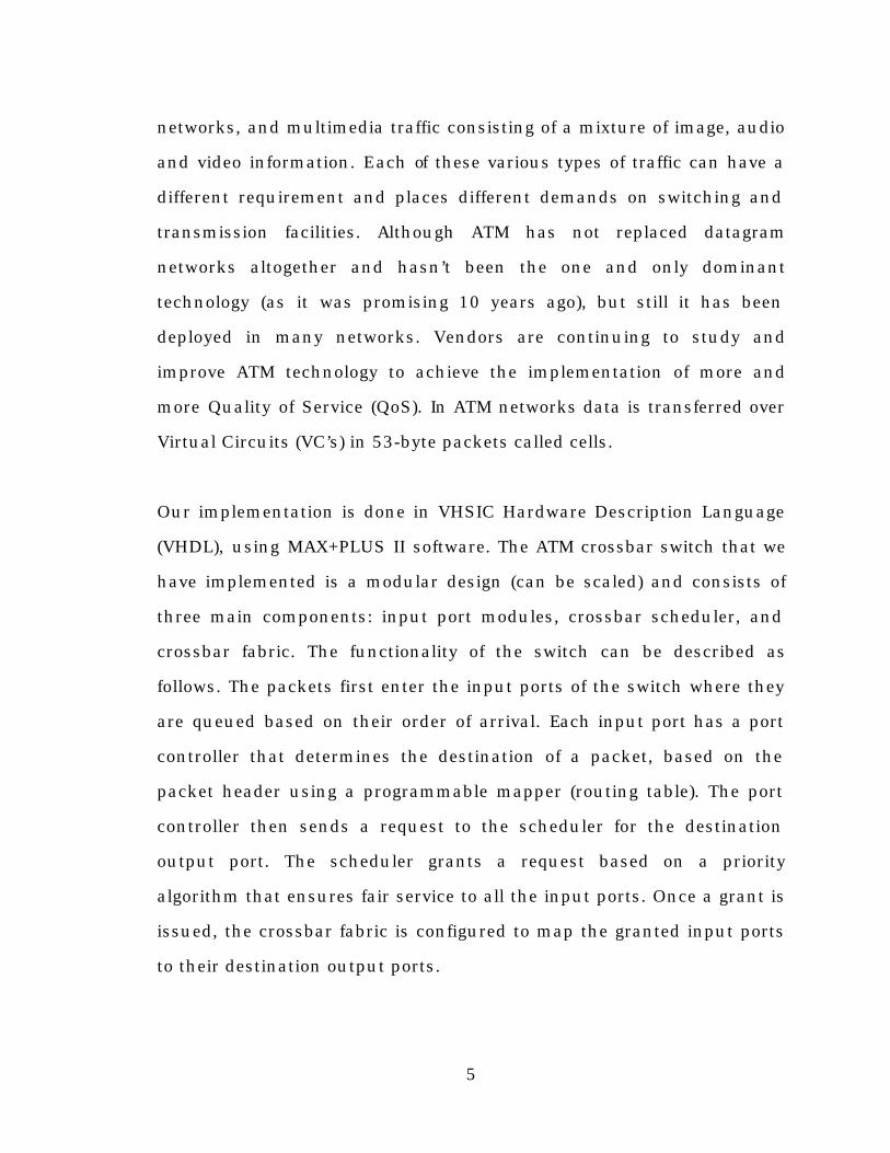
Figure 2.1: Schematic of a bus architecture switch with input port
processor (IPP), output port processor (OPP), and control processor [25].
In Figure 2.1, the input port processor (IPP) module processes the
incoming packets. Its functionalities include synchronizing the incoming
packets, looking up the packet header in routing tables, and updating
the header. The output port processors (OPP) module typically performs
some form of queuing and some congestion control. The control
processor configures the routing tables based on the user requests.
In a bus architecture switch, if the input/output line rate is R and there
are n ports, then the bus should have a minimum speed of Rn. This
means that, for a bus clock of r Hz, the bus has to be w = Rn/r bits wide.
This relation shows that the bus speed has to grow with the number of
links and that is a disadvantage for the bus architecture. Also, the
ControlProcessor
IPP OPP
9
problem of capacitive loading on the signal lines rises as the number of
ports connected to the bus increases. This reduces the maximum clock
frequency of the bus.
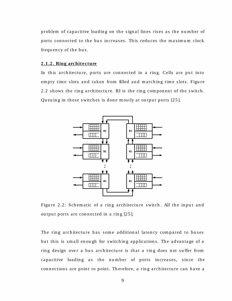
2.1.2. Ring architecture
In this architecture, ports are connected in a ring. Cells are put into
empty time slots and taken from filled and matching time slots. Figure
2.2 shows the ring architecture. RI is the ring component of the switch.
Queuing in these switches is done mostly at output ports [25].
Figure 2.2: Schematic of a ring architecture switch. All the input and
output ports are connected in a ring [25].
The ring architecture has some additional latency compared to buses
but this is small enough for switching applications. The advantage of a
ring design over a bus architecture is that a ring does not suffer from
capacitive loading as the number of ports increases, since the
connections are point to point. Therefore, a ring architecture can have a
RI
RI
RI
RI
RI
RI
10
larger number of ports. However, similar to bus architecture, the speed
of the ring has to increase as the number of ports grows. For a ring
supporting n input/output ports (each operating at a data rate of R bits
per second), the ring speed should be a minimum of Rn. As n increases
the speed of the ring has to increase too. This is similar to the limitation
that exists on bus architecture.
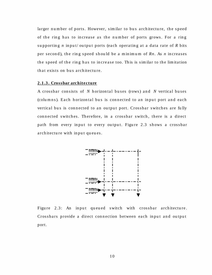
2.1.3. Crossbar architecture
A crossbar consists of N horizontal buses (rows) and N vertical buses
(columns). Each horizontal bus is connected to an input port and each
vertical bus is connected to an output port. Crossbar switches are fully
connected switches. Therefore, in a crossbar switch, there is a direct
path from every input to every output. Figure 2.3 shows a crossbar
architecture with input queues.
Figure 2.3: An input queued switch with crossbar architecture.
Crossbars provide a direct connection between each input and output
port.
11
The speed of the crossbar depends on whether input queues or output
queues are used. In case of input queues, the input and output port
controllers have the advantage of working with merely the speed of the
links. If output queues are utilized, the switch fabric has to be fast
enough not to cause contention at the output ports. Section 2.2
discusses input queuing vs. output queuing.
Crossbar-based systems can be significantly less expensive than bus or
ring systems with equivalent performance because the crossbar allows
multiple data transfers to take place simultaneously. Furthermore,
crossbars are non-blocking, which means any input-output pair can talk
to each other as long as they do not interfere with other input-output
pairs. However, in the absence of a fast scheduling algorithm the
crossbar becomes a performance bottleneck for big switches. Crossbars
are generally expensive, but compared to the total cost of a switch, the
crossbar component contributes only a small fraction (around 5%
according to [3]).
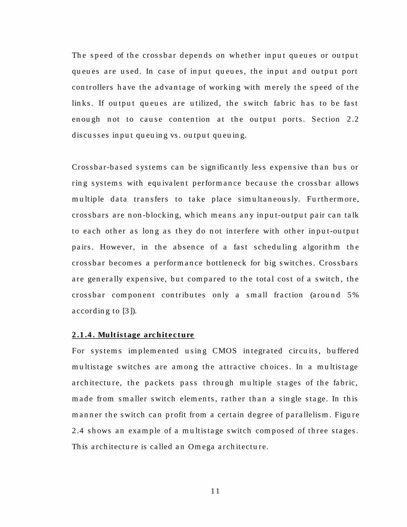
2.1.4. Multistage architecture
For systems implemented using CMOS integrated circuits, buffered
multistage switches are among the attractive choices. In a multistage
architecture, the packets pass through multiple stages of the fabric,
made from smaller switch elements, rather than a single stage. In this
manner the switch can profit from a certain degree of parallelism. Figure
2.4 shows an example of a multistage switch composed of three stages.
This architecture is called an Omega architecture.
12
Figure 2.4: An 8×8 Omega architecture is an example of a multistage
switch.
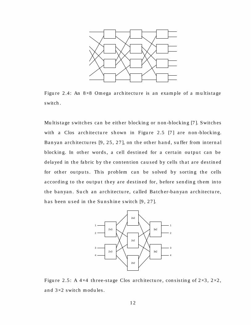
Multistage switches can be either blocking or non-blocking [7]. Switches
with a Clos architecture shown in Figure 2.5 [7] are non-blocking.
Banyan architectures [9, 25, 27], on the other hand, suffer from internal
blocking. In other words, a cell destined for a certain output can be
delayed in the fabric by the contention caused by cells that are destined
for other outputs. This problem can be solved by sorting the cells
according to the output they are destined for, before sending them into
the banyan. Such an architecture, called Batcher-banyan architecture,
has been used in the Sunshine switch [9, 27].
Figure 2.5: A 4×4 three-stage Clos architecture, consisting of 2×3, 2×2,
and 3×2 switch modules.
2x3
2x3
2x2
2x2
2x2
3x2
3x2
1
2
3
4
1
2
3
4
13
2.2. Buffering in packet switches
Even with a non-blocking interconnect such as the crossbar, some
buffering is necessary because packets that arrive at the interconnect
are unscheduled and the switch has to multiplex them. There are three
basic conditions where buffering is necessary: 1) The output port
through which the packet needs to be routed is blocked by the next
stage of the network. 2) Two packets destined for the same output port
arrive simultaneously at different input ports but the output port can
accept only one packet at a time. 3) The packet needs to be held while
the routing module in the switch determines the output port to which
the packet is sent.
The optimal place for the queues in high-performance switches has long
been studied. Here are some of the advantages and disadvantages of
input (IQ), central shared (CS), and output queuing (OQ).
2.2.1 Output queues
Output queues are used when the aggregate throughput of the switch
fabric and the memory is large enough to keep all the output links
continuously busy, therefore making the system highly efficient. In such
a case, quality of service (QoS) guarantees can be provided. For an N×N
switch, generally, output queuing is implemented when the switch fabric
runs at least N times faster than the speed of the input lines. This is a
disadvantage when high-speed port processors or fast switch fabrics are
not available. Another disadvantage of the output buffer is that in order
to be able to handle simultaneous packet arrivals, each output buffer
must have as many write inputs as there are input ports to the switch.
14
Implementing output buffers with multiple write inputs increases their
cost and reduces their performance. Furthermore, having more than one
write at a time can cause problems in buffer allocation for variable sized
packets [23].
2.2.2. Shared central buffers
Complete sharing of the buffering space by all the ports results in the
most efficient usage of memory resources. Hence, it would be ideal to
use central buffers. However, there are fundamental difficulties in the
efficient hardware implementation of switches with central buffers [23].
All the input ports and output ports access the shared central buffer;
hence in the worst case the bandwidth of the central buffer has to be
equal to sum of the bandwidth of all the ports. Furthermore for an N×N
switch, the central buffer has to at least have 2×N ports to be accessible
by all input and output ports. Multi-port memory is very expensive to
implement and leads to poor performance because of its large access
time. To avoid multi-port memories, it is possible to increase the buffer
and connection line widths. However, that will cause the bandwidth to
be wasted for cells that are smaller than the width of the bus. In addition
to implementation difficulties, shared central buffers cause some
performance problems. Complex control circuitry for variable size
packets and “hogging” of the output ports as some performance issues
examples are discussed in [23].
2.2.3. Input queues
One advantage of having input buffers in a packet switch is that the
buffer requires only one write port, because only one packet arrives at
an input port at a time. The fabric and memory of an input queued (IQ)
15
switch need to be merely as fast as the line rate. This makes input
queuing very appealing for switches with fast line rates or with large
numbers of ports. Note the latter is the consequence of the fact that if
output queues are chosen for an N×N switch, the fabric and memories
have to be N times faster than the line rates, and memory is not fast
enough as N increases. Moreover, for multicast traffic (traffic that is sent
from a single input port to multiple output ports), a burst of n cells that
are to be delivered to m output ports only needs n cell buffers for the IQ
structure, rather than m×n buffers for OQ structure. Furthermore, if the
buffer is a First in First Out (FIFO) buffer, it is very easy to deal with
variable size packets and avoid memory management problems.
The disadvantage of IQ switches with FIFO buffers is head of line (HOL)
blocking. HOL blocking occurs when a packet at the head of queue,
waiting for a busy output, blocks a packet behind it that is destined to
an idle output. HOL blocking can have the worst effect when the traffic is
periodic [3] and the scheduling algorithm is based on priority rotation.
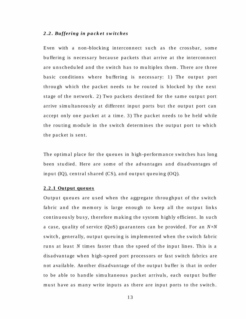
In such a case the throughput of the switch can be reduced to the
throughput of a single link. Figure 2.6 provides an example of periodic
traffic: in each time slot only one input and output can communicate
with each other.
Comparing output queuing with input queuing for non-blocking
switches [12] shows that in output queuing, 100% of the output
bandwidth can be utilized, while in input queuing the switch can be
loaded up only to a maximum of 58% due to HOL blocking. The 58%
utilization is achieved under the assumption that the input ports have
16
FIFO queues and the incoming traffic is governed by an independent
identical Bernoulli process. In other words, it is assumed that the
probability that a packet arrives at each input in any given time slot is
p, and each packet has the equal probability 1/N of being addressed to
any given output.
Figure 2.6: An input buffered switch with periodic traffic (worst case for
HOL blocking). The packet labels are the destination output port
numbers of arriving packets.
Many subsequent studies have tackled improving the performance of
input-queued packet switches. Some of the proposed techniques are as
listed below.
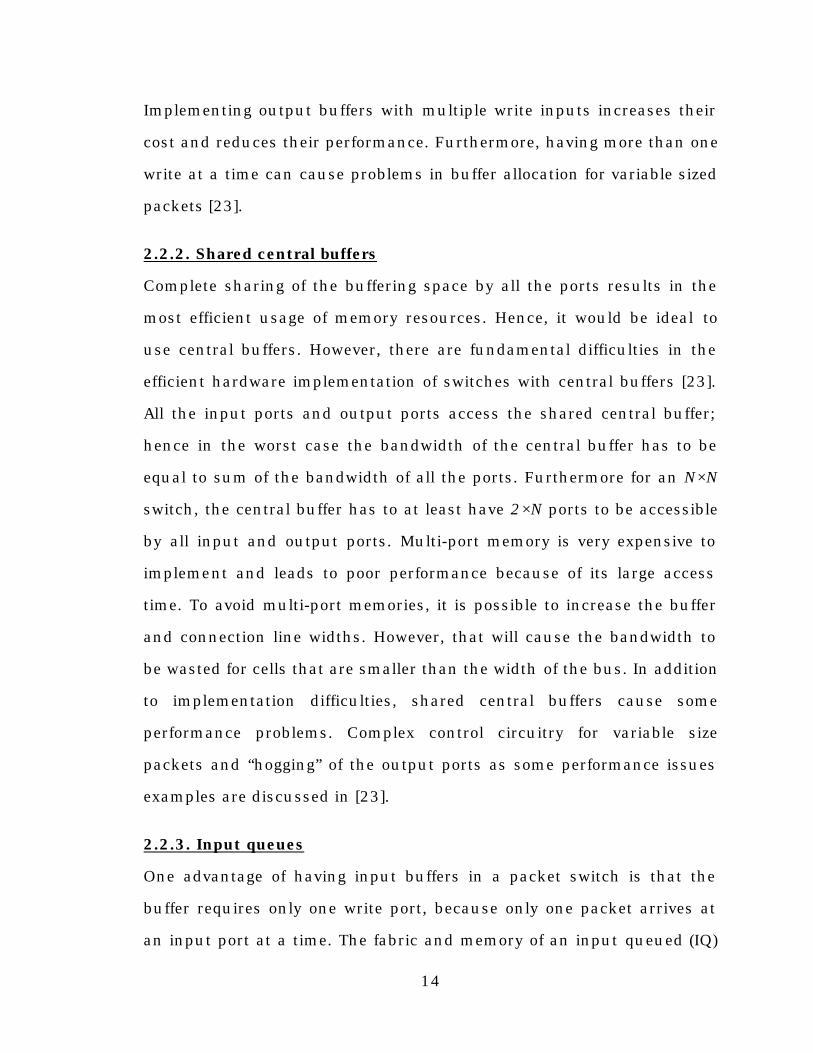
1) Using non-FIFO buffers: One scheme in this category is virtual
output queuing (VOQ) [3, 16, 21, 23]. In this scheme each input
has N queues or blocks of memory instead of one single FIFO
queue. In other words, there is a separate queue for each input-
output pair (Figure 2.7).
1
1
3 3 2 2 1 1
3 3 2 2 1 1
3 3 2 2 1
2 2 1 1
3 3 2 2 1
33
1
2
3
4
5
1
2
3
4
5
17
Figure 2.7: Simple virtual output queuing (VOQ) structure. This
architecture removes the HOL blocking effect [16].
There are three possible “multiple input queue” buffer structures [23].
Figure 2.8 shows these three schemes together with the standard FIFO
architecture. Item 2.8.(a) in the Figure is the standard FIFO queue
structure. It shows a 4×4 crossbar switch with a single FIFO buffer at
each input. Packets that arrive at each input of the switch are queued in
the buffer and served in the order that they arrived.
What follows is a description of the three “multiple input queue” buffer
structures -Figures 2.8.(b), (c), and (d).
A. Statically allocated fully connected (SAFC) buffer [23] shown in Figure
2.8.(b) eliminates HOL blocking by providing, at each input port, a
separate FIFO queue for every output port. At every input port, packets
A1
input 1Q1,1
Q1,N
input MQM,1
QM,N
AM
crossbar switchoutput 1
output N
18
that are destined for output 1 are sent to queue 1, packets destined for
output 2 are sent to queue 2, et cetera. When there is a separate FIFO
queue for each output (in this case there are four separate FIFO queues
at each input, corresponding to the four outputs of the switch) then
packets in every queue are contending for the same output. Hence, the
packet at the head of line cannot be blocking a packet behind it from
being sent to an idle output (and hence no HOL blocking exists). In this
architecture, every input can send N packets in every time slot (rather
than one packet in case of single FIFO inputs). This increases the
throughput of the switch.
The SAFC scheme has the following disadvantages:
i. Four separate crossbars must be controlled as opposed to a
single crossbar;
ii. Each input port requires four separate buffers and buffer
controllers;
iii. Buffer utilization is inefficient. The available buffer space is
partitioned into four statistically allocated queues. Hence,
the potential storage space for a given packet is only one
quarter of the buffer space at each input port;
iv. Pre-routing is required for every packet in order to
determine the destination output port (and hence the input
queue the packet belongs to).
19
Figure 2.8: Alternative designs of switches with input port buffers [23].
(a) Standard FIFO buffer, (b) N FIFO queues at each input (each FIFO
queue connected to a separate crossbar), (c) N FIFO queues at each
input (only one queue at each input port connected to the crossbar at
any time), (d) N FIFO queues (with dynamic boundaries) at each input
share the same buffer.
B. Statically allocated multi -queue (SAMQ) buffer shown in Figure 2.8.(c)
removes disadvantage i. from the list by sacrificing the high throughput
[23]. Each input can send only one packet to the crossbar in every time
slot (as opposed to N in the previous case). This removes the need to
inputports
a) FIFO buffers
output ports
crossbar
N
inputports
b) statically allocated fullyconnected (SAFC)
N/4
output ports
4x14x14x14x1
d) dynamically allocatedmulti-queue (DAMQ)
inputports
output ports
N
crossbar
c) statically allocatedmulti-queue (SAMQ)
inputports crossbar
output ports
N/4
20
control N crossbars at any time. Nevertheless, the remaining
disadvantages of the SAFC buffers still exist.
C. Dynamically allocated multi -queue (DAMQ) buffer [23] shown in
Figure. 2.8.(d) has none of the disadvantages mentioned earlier. In this
scheme each input buffer uses a single buffer pool. Virtual queues are
allocated dynamically within each input buffer and that makes the
buffer usage more efficient. Each virtual queue is maintained via a
linked list. For each virtual queue, there is a head/tail register pointing
to the head and tail of the corresponding linked list. A separate linked
list is also maintained for the free storage space in the buffer. When a
packet arrives, it is written to the memory location marked by the head
of the free space linked list (no pre-routing required). While the packet is
being written to the free buffer space, its header is looked up and its
destination output port number is determined. The tail pointer of the
link list corresponding to this output port destination will then change,
to point to the arrived packets location.
2) Operating the switch fabric at a faster speed than the input/output
lines (speedup): This scheme reduces the effect of HOL blocking but
does not remove it completely [6]. A speedup by a factor of S can remove
S packets from each input port within each time slot. Therefore, for an
N×N switch, if output buffers are used, the speedup is N, and if input
buffers are used, the speedup is equal to one. For switches that use
speedup, both input and output buffers are required.
21
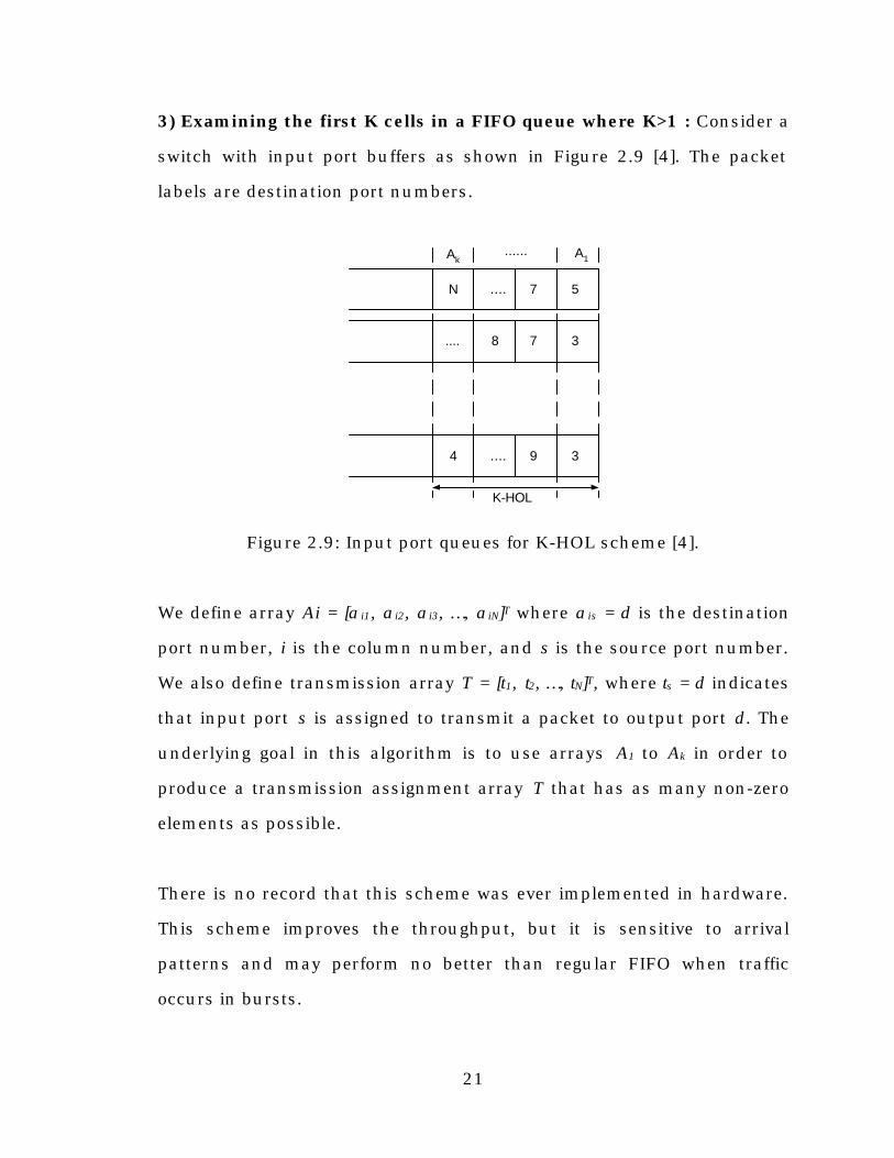
3) Examining the first K cells in a FIFO queue where K>1 : Consider a
switch with input port buffers as shown in Figure 2.9 [4]. The packet
labels are destination port numbers.
Figure 2.9: Input port queues for K-HOL scheme [4].
We define array Ai = [a i1, ai2, ai3, …, aiN]T where a is = d is the destination
port number, i is the column number, and s is the source port number.
We also define transmission array T = [t1, t2, …, tN]T, where ts = d indicates
that input port s is assigned to transmit a packet to output port d. The
underlying goal in this algorithm is to use arrays A1 to Ak in order to
produce a transmission assignment array T that has as many non-zero
elements as possible.
There is no record that this scheme was ever implemented in hardware.
This scheme improves the throughput, but it is sensitive to arrival
patterns and may perform no better than regular FIFO when traffic
occurs in bursts.
57....N
37
39....4
.... 8
K-HOL
A1......Ak
22
2.3. Scheduling algorithms
The scheduler module in a packet switch decides when data is sent from
particular inputs to their desired outputs. Normally, a request is sent
from the input ports to the scheduler and the scheduler finds the best
configuration of input-output pairs. The scheduling algorithm has to be
fast, fair, and easy to implement in hardware. A comparison of several
scheduling algorithms for input queued switches can be found in [17].
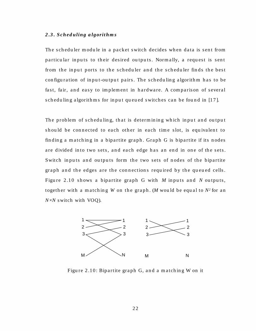
The problem of scheduling, that is determining which input and output
should be connected to each other in each time slot, is equivalent to
finding a matching in a bipartite graph. Graph G is bipartite if its nodes
are divided into two sets, and each edge has an end in one of the sets.
Switch inputs and outputs form the two sets of nodes of the bipartite
graph and the edges are the connections required by the queued cells.
Figure 2.10 shows a bipartite graph G with M inputs and N outputs,
together with a matching W on the graph. (M would be equal to N2 for an
N×N switch with VOQ).
Figure 2.10: Bipartite graph G, and a matching W on it
1
2
3
M
21
3
N
1
2
3
M
21
3
N
23
What follows is a description of several scheduling algorithms discussed
in literature.
1) Maximum Size Matching scheduling algorithm by McKeown,
Anantharam, and Warland [16] finds the matching that contains the
maximum number of edges. This algorithm is stable (and achieves 100%
throughput) for independent uniform traffic but could lead to starvation
(and hence queue overflow) or instability, if the arrival processes are not
uniform [16]. Maximum size matching can also cause a reduced
throughput for non-uniform traffic [20]. For non-uniform traffic, cells
concentrate among a relatively small number of VOQ’s and therefore,
the scheduling algorithm will not have many configurations to choose
from. If the traffic is uniformly distributed among all the VOQ’s, the
algorithm will have different choices in finding the maximum matching
and will result in a higher throughput. In other words, the main problem
with maximum size matching is that it does not consider the backlog of
cells in the VOQ’s, or the cells that have been waiting in line to be
served. Furthermore, this algorithm is too complex to implement in
hardware. The best known maximum size matching algorithm converges
in O(n5/2) time [15].
2) Maximum Weight Matching algorithm assigns a weight to each
input queue [16]. The matching algorithm finds an input-output match
that has the highest sum of weights. This algorithm is stable for both
uniform and non-uniform traffic [16]. The weight assigned to each queue
is usually equal to the occupancy of the queue and therefore the longest
queue has the highest weight. Hence this algorithm is also called
24
Longest Queue First (LQF). The disadvantage of maximum weight
matching is its high complexity i.e., O(N3logN). The algorithm can not be
implemented in hardware because it needs multi-bit comparators to
compare the weights of the queues.
3) Oldest Cell First (OCF) scheduling leads to 100% throughput for
independent arrivals and no queue will be starved [21]. This algorithm
uses the waiting times of HOL cells as requesting weights and selects a
match such that the sum of all queue waiting times is maximized. This
algorithm, however, is too complex (i.e., O(N3logN)) to be implemented in
hardware.
4) Longest Port First (LPF) algorithm by McKeown is a variation of the
LQF scheme [20]. However it does not have the complexity of LQF and
can be implemented in hardware. In LQF algorithm, each queue has a
weight equal to the length of the queue. In LPF, however, the weight
(also called port occupancy) of each queue is the sum of aggregate input
and output queue occupancies. This algorithm finds the match that is
both maximum size and maximum weight. The complexity of the LPF
scheme is O(N2.5), but it can be simplified with some approximations in
order to be implemented in hardware.
5) Parallel iterative matching (PIM) algorithm is based on randomness
and iteration [15]. There are three steps in choosing the match between
inputs and outputs:
a. Each unmatched input sends a request to every output for
which it has a queued cell;
25
b. If an unmatched output receives any request, it grants one
by randomly selecting a request;
c. If an input receives a grant, it accepts one by selecting an
output randomly among those that granted its request.
These three steps are repeated for the inputs that are not paired with
any outputs, until they converge to a maximal match. A maximal match
is one in which each node is either matched or has no edge to an
unmatched node.
In the PIM algorithm, randomness prevents queues from being starved.
Also, in each iteration of random matching, a minimum average of 3/4 of
the remaining possible connections are matched or eliminated.
Therefore this algorithm converges to a maximal match in an average of
O(log N) iterations. The disadvantage of this randomness is that it is
expensive and difficult to implement in hardware. Furthermore, it can
lead to unfairness between connections and the multiple iterations are
time consuming. We prefer an algorithm that performs well in a single
iteration.
6) Round robin matching (RRM) overcomes the unfairness of random
matching by granting requests and accepting grants according to a
round robin priority scheme [15, 18]. There are three steps in this
algorithm shown in Figure 2.11:
a. In the Request step, each input sends a request (arrows in
Figure 2.11) to every output for which it has a queued cell;
b. In the Grant step, an output that has received any requests
grants the one request that appears next in a fixed round
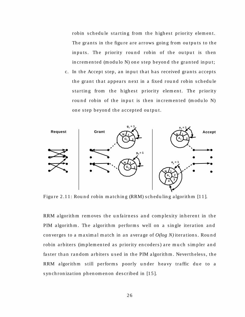
26
robin schedule starting from the highest priority element.
The grants in the figure are arrows going from outputs to the
inputs. The priority round robin of the output is then
incremented (modulo N) one step beyond the granted input;
c. In the Accept step, an input that has received grants accepts
the grant that appears next in a fixed round robin schedule
starting from the highest priority element. The priority
round robin of the input is then incremented (modulo N)
one step beyond the accepted output.
Figure 2.11: Round robin matching (RRM) scheduling algorithm [11].
RRM algorithm removes the unfairness and complexity inherent in the
PIM algorithm. The algorithm performs well on a single iteration and
converges to a maximal match in an average of O(log N) iterations. Round
robin arbiters (implemented as priority encoders) are much simpler and
faster than random arbiters used in the PIM algorithm. Nevertheless, the
RRM algorithm still performs poorly under heavy traffic due to a
synchronization phenomenon described in [15].
g1 = 1
G1
N 1
2
a1 = 1
A1
N 12
34
a3 = 1
Request Grant Accept
A1
N 1
2
G2
N 1
2
g3 = 1
27
7) iSLIP is an iterative algorithm achieved by making a small change to
the RRM scheme [15]. iSLIP has the same three steps of RRM. Only the
second step (Grant step) has changed and changed little:
b. If an output receives any requests, it grants one that appears
next in a fixed round robin schedule starting from the
highest priority queue. However, the round robin at the
output is not incremented (module N), unless the grant is
accepted by the input in the Accept step. In other words, the
priority round robin at the output side is incremented
(provided that the grant was accepted) after the Accept step
is passed.
Those inputs and outputs not matched at the end of one iteration are
eligible for matching in the next. This small change to the RRM
algorithm makes iSLIP capable of handling heavy loads of traffic and
eliminates starvation of any connections. The algorithm converges in an
average of O(log N) and a maximum of N iterations. iSLIP can fit in a
single chip and is readily implemented in hardware [17].
3.3. Examples of existing ATM switches
The Knockout switch has a non-blocking, fully connected internal
interconnect (fabric) [26, 27]. It is a modular switch with output FIFO
buffers and a maximum line rate of 50 Mbps. The switch does not have a
time-slot specific scheduling algorithm and multiple simultaneous
packets can arrive at any output buffer. Up to 1000×1000 switches can
be implemented employing the knockout fabric architecture.
28
The ForeRunner ASX-200 switch is an example of a modular bus
architecture ATM switch [8] with shared memory output buffers. It
supports up to 32 ATM ports ranging in speeds from T1/E1 (1.544 Mbps)
to OC-12c/STM-4c (622 Mbps).
The Tiny Terra switch is an input buffered switch with a crossbar fabric
architecture [18]. This 32×32 switch employs VOQ mechanism, and an
iSLIP scheduling algorithm [15]. The maximum line rate of the switch is
10 Gbps.
The 16×16 ATLAS I single chip ATM switch has a maximum line rate of
622 Mbps [13]. The switch employs shared output buffers. The ATM cells
are stored in the single shared buffer pool and are never moved until
they depart the switch. The scheduling algorithm of the switch is priority
based. Certain ATM cells have higher priorities and are scheduled to
leave the switch earlier than other cells.
The 32×32 Sunshine switch has output buffers and a self-routing
Batcher-banyan fabric [9]. Input and output lines have a data rate of 155
Mbps. Input cells are queued according to four service classes and are
output in a round robin manner.
In the design of the switch, presented in the next 5 chapters, we have
chosen a crossbar fabric because it is a fully connected, non-blocking,
and fast architecture. Input buffers are used to benefit from the
advantages of input buffering discussed earlier in this chapter. To
overcome the HOL blocking phenomenon inherent in FIFO input
29
buffers, we have employed the VOQ architecture. The scheduling
algorithm used in the switch discussed in Chapter 5 is a fair, fast,
simple, and efficient algorithm that can easily be implemented in
hardware.
30
Chapter 3
High-level switch view
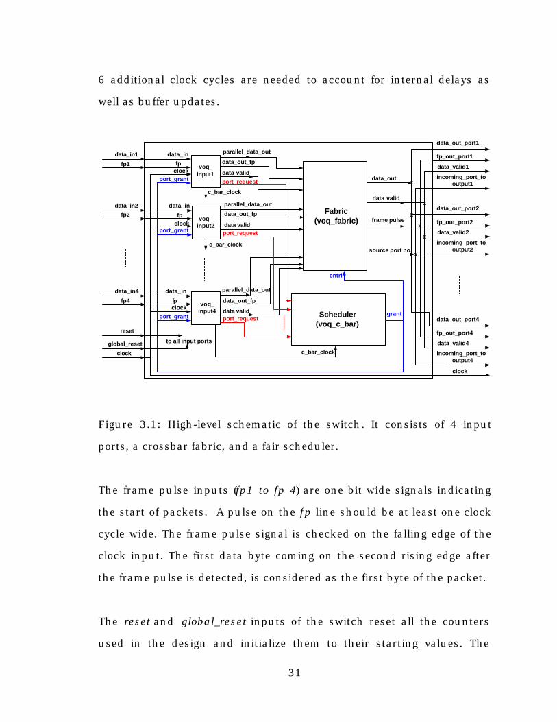
The overall view of the 4×4 switch design is given in Figure 3.1. The
input lines to the switch are four data lines, four frame pulse inputs, one
clock input, a reset input, and a global reset input. The output lines of
the switch are 4 data output lines, 4 data valid lines, 4 output frame
pulse lines, one clock output, and 4 outputs that indicate the origin of
the data coming to each data output port. This switch is modular and
can be scaled up or down with minor changes. A more detailed
schematic of our 4×4 switch design is available in Appendix A.
The four data inputs (data_in1 to data_in4) are each 8 bits wide, and
carry fixed size Asynchronous Transfer Mode (ATM) packets. Other
packet formats such as IP packets have to be fragmented into ATM cells
first and before being input to the switch. One data byte can be input to
the switch in every clock cycle. In our switch, data is both input and
output on the rising edge of the clock.
The clock input is global to all switch components. It is used to clock the
input and output data streams. Another clock called c_bar_clock is
internally generated within the input port modules. This clock has a
period equal to a packet time. Packet time is the interval required for a
packet to be output from the switch. The length of the packet time is
dependent on the frequency of the clock inputs. The rule of our design
is that the c_bar_clock should be 59 times slower than the clock input.
For the 53 bytes in an ATM packet, 53 clock cycles are required and the
31
6 additional clock cycles are needed to account for internal delays as
well as buffer updates.
Figure 3.1: High-level schematic of the switch. It consists of 4 input
ports, a crossbar fabric, and a fair scheduler.
The frame pulse inputs (fp1 to fp 4) are one bit wide signals indicating
the start of packets. A pulse on the fp line should be at least one clock
cycle wide. The frame pulse signal is checked on the falling edge of the
clock input. The first data byte coming on the second rising edge after
the frame pulse is detected, is considered as the first byte of the packet.
The reset and global_reset inputs of the switch reset all the counters
used in the design and initialize them to their starting values. The
fp
fp
Fabric(voq_fabric)
voq_input1
data_in
clockport_grant
parallel_data_out
data_out_fp
data valid
voq_input2
data_in
fpclock
port_grantdata validport_request
data_in
clock
port_grantdata validport_request Scheduler
(voq_c_bar)grant
data_out
source port no.
data valid
frame pulse
clock
global_reset
reset
data_in4
fp4
data_in2
fp2
data_in1
fp1
data_out_port1
fp_out_port1
data_valid1
incoming_port_to_output1
data_out_port4
fp_out_port4
data_valid4
incoming_port_to_output4
data_out_port2
fp_out_port2
data_valid2
incoming_port_to_output2
x
x
x
x
x
to all input ports
voq_input4
port_request
data_out_fp
data_out_fp
parallel_data_out
parallel_data_out
x
c_bar_clock
cntrl
clock
c_bar_clock
c_bar_clock
32
global_reset signal resets the input buffers, where the ATM packets are
stored, as well. In other words, if an error occurs while switching a
packet, the reset signal can be used to switch that packet again.
However, if one wants to reset the whole switch and delete the contents
of the buffers, global_reset should be used.
The output ports in our switch do not have any processing capability or
any storage capacity. They are currently only the pins of the chip. An
output module such as the one described in Appendix B can be
implemented at the output ports to reassemble the packets and store
them until they are allowed to enter the network. Currently, the output
lines of our switch are clock, data_out_port, fp_out_port, data_valid, and
incoming_port_to_output.
The output data bytes are sent out on data_out_port1 to data_out_port4
output ports. The output frame pulse signals (fp_out_port1 to
fp_out_port4 ) generated within the switch mark the beginning of
outgoing packets for their corresponding data lines. The relationship
between the beginning of the packet and the frame pulse for the output
ports is similar to that of the inputs: the first byte of an outgoing packet
is sent out on the second rising edge of the output clock after a pulse on
the corresponding output’s frame pulse lines is detected. (The frame
pulse line is checked on the falling edge of the clock.)
The data_valid output lines (data_valid1 to data_valid4) indicate whether
the data present at the corresponding output of the switch is valid for
33
sampling. If this line is logic low, the corresponding output line is invalid
and should be ignored.
A source port number signal (incoming_port_to_output1 to incoming
port_to_output4) is available at each output port along with the data. This
signal indicates at which input port the data originated. This signal can
later be used for classifying and outputting the data according to a
desired priority scheme. Furthermore, in cases where the packets are
partially switched, the origin of each packet can be used to reassemble
the data at the output ports. This matter is discussed further in
Appendix B.
Appendix C contains the VHDL source code for the voq_switch project
and all the components in the switch.
34
Chapter 4
Input ports
There is an input port module for each of the four inputs of our 4×4
switch. This module is responsible for handling, storing and processing
the arriving ATM packets. This document refers to the input port module
as the “voq_input” module. VOQ stands for virtual output queuing
described in earlier chapters. VOQ has been implemented in the input
port modules of our switch; hence its name.
A high-level schematic of the voq_input module is shown in Figure 4.1.
Each data byte arriving at the voq_input module is first written into a
Random Access Memory (RAM) component called bufferx. This buffer
holds up to 848 one-byte words. The second, third and fourth bytes of
the packet are written into VCI registers as well as the buffer. These
bytes, located in the header of the ATM packet, contain the Virtual
Circuit Identifier (VCI) information. Figure 4.2 shows an ATM cell with its
header and payload bytes.
Figure 4.1: High-level schematic of voq_input module of the switch.
input data
output data
request grant
bufferx
port controller
port LUT
VCIregisters
35
(a) (b)
Figure 4.2: (a) An ATM cell consisting of a 5 byte header and a 48 byte
payload. (b) The User Network Interface (UNI) ATM cell header. Bytes 2,
3, and 4 contain the VCI information.
Depending on the VCI information in the packet header, the ATM switch
decides to which output port the ATM packet should be sent, and what
the new VCI should be. In this document, “VCI bytes” refers to the
second, third, and fourth bytes of the ATM header shown in Figure
4.2.(b). Those 16 bits that are marked as VCI in this Figure are in turn
called “VCI bits”.
After the first four bytes of a packet are read, and while the rest of the
bytes of the packet are being shifted in, the port controller extracts the
address information (VCI bits) from the header of the arriving ATM
packet and sends it to a Look Up Table (LUT) module. The LUT is a
routing table that updates the VCI bytes of the header and returns the
new VCI together with the destination output port number for that
packet. The port controller then sends a request for that specific output
port to the scheduler, and awaits a grant.
Once a grant is issued for a certain packet, the data bytes are de-queued
from the input buffer in the order that they had arrived. A counter for
GFC VPI
VPI VCI
VCI
VCI PT CLP
HEC
8 7 6 5 4 3 2 18 7 6 5 4 3 2 1
5 byteATM header
48 byteATM payload
36
the de-queue state machine within the port controller signals when the
updated VCI bytes have to be read from the VCI registers.
After the entire packet is sent, the same process is repeated for the next
packet. Note that as soon as a grant for an output port is issued, the
input port number is sent to the crossbar fabric so that the output port
receiving the data knows where the packet originated from. Figure 4.3
shows a detailed schematic of the voq_input module. In this Figure there
is no central controller. The input port controller is actually a gathering
of several seperate state machines shown in Figure 4.3:
1. Write sequence state machine (Write_seq_SM process);
2. VCI controller state machine (VCI_SM process);
3. Read sequence state machine (Read_seq_SM process);
4. Linked list update state machine (Linked_list_update process).
The following sections describe the main components of the voq_input
module (buffer, counters, LUT, VCI registers), and all the state machines
mentioned earlier.
4.1. Input buffer
The input buffer in our switch design shown in Figure 4.4 is a 848 word
dual port RAM. Each word is one byte wide. In order to address all the
words in the 848 word RAM the address lines are 10 bits wide. The write
address (wraddress) determines to where in the buffer the input data
bytes should be written, and the read address (rdaddress) is where the
37
outgoing data bytes are read from. There is a separate enable input for
both read and write operations (rden and wren). Read and write
operations are synchronized with the rising edge of the main clock of the
switch.
Each input buffer is divided into 16 virtual blocks of 53 bytes length,
shown in Figure 4.4. Every block is addressed with a pointer to its first
byte and can hold one complete ATM packet. The choice buffer size is a
trade off between the switch speed and the loss rate. The larger the
buffer is, the smaller the probability of buffer overflow and the loss rate.
On the other hand, the queuing delay increases as the buffer size grows.
A large queuing delay reduces the switching speed and results in a low
Quality of Service (QoS) in the network. For our 4×4 switch with input
buffers, 16 is a reasonable number that does not cause overflow for
uniform constant bit rate traffic.
We require 4-bit-wide pointers to reference individual blocks. While de-
queuing (or en-queuing) packets, it suffices to have a pointer to the
beginning of the block that holds (or will be holding) the packet. The
read and write counters provide the offset for read and write addresses.
The buffer in our design consists of five dynamic first in first out (FIFO)
queues. The queues are dynamic in the sense that they do not have
fixed sizes or locations in the buffer memory. Each block of the buffer
could belong to any of these five queues.
38
Figure 4.3: Voq_input module data path. It consists of two counters, a
RAM component (bufferx), a ROM based look-up table (LUT), and four
state machine based controllers.
data_in
8
8
8
q wren rden
wraddress rdaddress
bufferx
rdclock
wrclock data
wr_en_signal
RAM_out
wr_address_signal
9
6
aset
qcounter_53
clock
count53
clock
Write_seq_SM
clockfp
c53sset
count53
VC
I_reg_en
rd_address_signal
rd_en_signal
9Read_seq_SM
data
_out
_fp
dq_c
53ac
lr
aclr
qdq_counter53
clock
dq_count53
6
data_out_select
clock
reset
global_reset
dq_count53
port_grant
enable dataVCI_register2
clock q
data_in
VCI_reg2_out
VCI_reg1_out
enable dataVCI_register1
clock q
enable dataVCI_register0
clock q
VCI_reg0_out
8
8
8
8
8
8
vci_in_vector
data_in
8
clock
clock
clock
clock
clock
port_LUT
output_vci
output_port_no
input_vci
4
16
16VCI_SM
vci_in_vector(19 downto 4)
input_vci
clockenable
resetglobal_reset
resetglobal_reset
clock
count53
6
out_vci_ready
loadi
vci_out_vector
vci_out_vector(i)
clock
clock
MUX
prallel_data_out8
linked_list_update_SM
clock
reset
global_reset
free_spacequeue
next_register
count53
dq_count53
free_spacefrom the linked listupdate state machine
from counter_53 anddq_counter53
prallel_data_out
39
Figure 4.4: The structure of the buffer in each voq_input module. The
buffer is a 848 word RAM divided into 16 blocks.
The five FIFO queues are maintained via linked lists. A certain structure
called “queue_descriptor” is defined in VHDL for this purpose. Queue 1
to queue 5 in our design are of “queue_descriptor” type. The
“queue_descriptor” structure has three fields: head, tail, and empty.
address
bloc
k 0
bloc
k 1
bloc
k 2
bloc
k 15
pointer = "0000"
pointer = "0001"
pointer = "0010"
pointer = "1111"
... ...
... ...
847846
795794793
159158157
107106105
535251
210
next_register(15)
vci_out_vector(15)
ready_flag(15)
next_register(2)
vci_out_vector(2)
ready_flag(2)
next_register(1)
vci_out_vector(1)
ready_flag(1)
next_register(0)
vci_out_vector(0)
ready_flag(0)
1 byte
40
Head and tail fields are of type pointer and empty field is a one bit flag.
The head and tail fields of each queue point to the first and last blocks
in the queue, respectively. A logic high value for the empty field of a
queue shows that the queue is empty.
Four of the queues, queue(0) to queue(3), correspond to the four output
ports of the switch. In other words, packets that are destined for output
1 are stored in queue(0). The packets destined for output 2 are stored in
queue(1), etc. The fifth dynamic FIFO queue of the buffer is the
free_space queue. This queue holds the empty blocks of the buffer. Note
that an empty free_space queue is the equivalent of a full buffer. An
empty free_space queue indicates that there is no free block left to
accept a new packet.
Whenever a packet arrives at the buffer, it is written into the block that
is at the head of the free_space queue. Whenever a packet is to be read
from the buffer and sent to a certain output port, it is read from the
head of the queue that corresponds to that output port.
Each block of memory in our buffer (refer to Figure 4.4) has three
registers associated with it.
� The “next_register”: Let’s assume that block x holds a packet that
belongs to queue(i). The value of next register for block x -
next_register(x) - is the location of the next block belonging to queue(i).
This is how the members of different queues are distinguished, and
how the order of the blocks in each queue is accounted for. A detailed
41
description of how the linked lists are manipulated is given in section
4.8, where the linked_list_update process is described.
� The “vci_out_vector”: The vci_out_vector(x), associated with block x, is
where the updated VCI bytes of the packet in block x are stored.
� The “ready_flag”: The third register associated with each block x is
ready_flag(x). A logic high value of the ready_flag(x) indicates that an
ATM packet has been completely written into block x. A logic low
ready_flag shows that the corresponding block of the buffer is empty.
4.2. Counters
There are two main counters used in our design: counter_53 and
dq_counter53 (refer to Figure 4.3). Both these counters are always
enabled and will be incremented at the rising edge of the main clock, if
they are neither set nor cleared by their controllers. There is also a
third counter in our design called the clock_gen_counter. This counter is
a Mod(59) counter and assists in making the c_bar_clock signal.
The first counter, counter_53, is 6 bits wide and counts the number of
bytes that enter the voq_input module and are written (en-queued) into
the input buffer. This counter is mainly controlled by the write_seq_SM
controller shown in Figure 4.3. The counter is always kept in a set
condition and starts counting from zero once a frame pulse on the fp
input of the voq_input module signals the beginning of a packet. This
counter is set again, once the whole packet is read.
42
The second counter, the dq_counter53, is also a 6 bit counter. It is used
for reading (de-queuing) the data bytes from the input buffer. This
counter is mainly controlled by the Read_seq_SM controller shown in
Figure 4.3. This controller enables the counter when a packet in the
buffer receives a grant and is being de-queued from the buffer. The
counter is cleared once a whole packet has been de-queued and the
queues have been updated.
4.3. Look-up table (port_LUT)
The port_LUT is a Read Only Memory (ROM) based component that can
be initialized with an arbitrary set of data, to form the routing table of
the switch. The ROM has eight rows and each row is 36 bits wide. These
bits consist of: a 16-bit input VCI, a 16-bit output VCI, and a 4-bit output
port number. Figure 4.5 shows the LUT ROM in more detail.
The LUT component searches through the ROM rows, until it finds a
match between the input VCI bits in the ROM and the input_vci input to
the LUT. If the match exists on row x of the ROM, the output VCI bits
and the output port number bits in row x are displayed on output_vci
and output_port_no outputs of the LUT component, respectively. The
renable output is activated at the same time in order to signal that valid
data is on the output ports of the LUT. If no match is found in the table,
the output lines are all set to zero.
43
Figure 4.5: The port_LUT component is based on an 8 word ROM, where
each word is 36 bits wide.
4.4. VCI registers
The VCI registers shown in Figure 4.3 (VCI_reg0, VCI_reg1, and
VCI_reg2) are 8-bit wide registers. The input data lines of these registers
are loaded into them (on the rising edge of the clock), provided that the
registers are enabled. The outputs of these registers are concatenated
and stored in a separate register called vci_in_vector.
Upon the arrival of VCI bytes, the voq_input module enables the VCI
registers. Three clock cycles after they are enabled, the registers will be
holding correct VCI bytes, and vci_in_vector will have a valid value.
port_lut
input_vci
16
output_vci
output_port_no
ROM
clock
renable
output VCIoutput port
number
input VCI output VCIoutput port
number
input VCI output VCIoutput port
number
input VCI output VCI output portnumber
input VCI
ROMaddress
7
6
5
2
1
0
1 2 ... 15 16,17 18 ... 32,33 34 ... 36
16
4
input VCI output VCI output portnumber
44
4.5. Write sequence controller (Write_seq_SM state machine)
The write sequence controller module (Write_seq_SM) shown in Figure
4.3 is comprised of a state machine called Write_seq_SM shown in
Figure 4.6.a. This state machine has two states: S0 and S1. All the state
transitions happen at the falling edge of the clock, and in each state the
condition of reset is checked, as shown in "Reset check in write
sequence state machine" diagram (Figure 4.6.b.)
Figure 4.6.a: Write sequence state machine in each input port module
(write_seq_SM process in voq_input.vhd file of Appendix C)
The write sequence state machine, starts from state zero (S0) where all
the signals are reset and the counter_53, which counts the number of
written bytes, is set to all ones. The state machine remains in state zero
count53 = 1 or 2or 3
1
wr_en_signal = '0'VCI_reg_en = '0'
fp = '1' ANDfree_space.empty = '0'
wr_address_signal = count53 + (( free_space.head) * 53)wr_en_signal = '1'
temp =free_space.head
c53sset = '0'
c53sset = '1'
S0
S1
1
0
count53 = 53
1c53sset = '1'
0
VCI_reg_en = '1'
0
VCI_reg_en = '0'
45
until a pulse on the fp input line indicates that a new packet is arriving.
(The fp line is sampled on every falling edge of the clock.) Upon
detection of a pulse on the fp line, if the buffer is not full, the state
machine goes to state one (S1). In state one the arriving packet is written
to the block that is at the head of the free_space FIFO queue (more on
this later when we describe the linked list updates). The write address
first points to the first byte of the block at the head of free_space queue,
and moves forward as the counter_53 counts. This counter is
incremented by one for each incoming data byte, and moves the write
address pointer forward to the next position in the block.
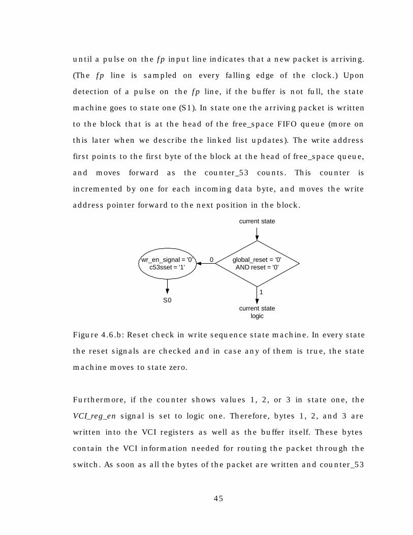
Figure 4.6.b: Reset check in write sequence state machine. In every state
the reset signals are checked and in case any of them is true, the state
machine moves to state zero.
Furthermore, if the counter shows values 1, 2, or 3 in state one, the
VCI_reg_en signal is set to logic one. Therefore, bytes 1, 2, and 3 are
written into the VCI registers as well as the buffer itself. These bytes
contain the VCI information needed for routing the packet through the
switch. As soon as all the bytes of the packet are written and counter_53
global_reset = '0'AND reset = '0'
current state
current statelogic
1
0wr_en_signal = '0'c53sset = '1'
S0
46
reaches 53, the state machine goes back to state zero where it awaits the
arrival of a new packet.
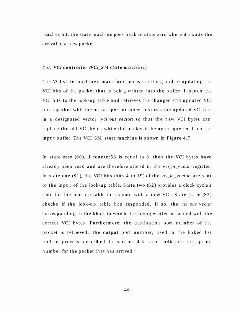
4.6. VCI controller (VCI_SM state machine)
The VCI state machine’s main function is handling and to updating the
VCI bits of the packet that is being written into the buffer. It sends the
VCI bits to the look-up table and retrieves the changed and updated VCI
bits together with the output port number. It stores the updated VCI bits
in a designated vector (vci_out_vector) so that the new VCI bytes can
replace the old VCI bytes while the packet is being de-queued from the
input buffer. The VCI_SM state machine is shown in Figure 4.7.
In state zero (S0), if counter53 is equal to 3, then the VCI bytes have
already been read and are therefore stored in the vci_in_vector register.
In state one (S1), the VCI bits (bits 4 to 19) of the vci_in_vector are sent
to the input of the look-up table. State two (S2) provides a clock cycle’s
time for the look-up table to respond with a new VCI. State three (S3)
checks if the look-up table has responded. If so, the vci_out_vector
corresponding to the block to which it is being written is loaded with the
correct VCI bytes. Furthermore, the destination port number of the
packet is retrieved. The output port number, used in the linked list
update process described in section 4.8, also indicates the queue
number for the packet that has arrived.
47
Figure 4.7: VCI state machine in each input port module. (VCI_SM
process in the voq_input.vhd file of Appendix C)
In state three, if the look-up table does not output a valid output_vci by
the time the whole packet is shifted into the buffer, then the state
machine goes back to state zero. In such a case, the output port number
and the vci_out_vector register of the block that received the packet will
both be zero. Hence, if a packet with an unknown VCI (a VCI that does
not exist in the LUT) arrives at our switch, the default updated VCI and
the default destination port number of the packet will be set to zero.
S0
S1
S2 S3
S4
count53 = 3
input_vci = vci_in_vector (19 downto 4)
0
1
out_vci_ready
1
count53 = 52 0
0
1
vci_out_vector (free_space.head, 23 downto 20) <= vci_in_vectorvci_out_vector (free_space.head, 19 downto 4) <= output_vcivci_out_vector (free_space.head, 3 downto 0) <= vci_in_vector
destination_port_no <= output_port_no
48
4.7. Read sequence controller (Read_seq_SM state machine)
The read sequence controller implements the Read_seq_SM state
machine shown in Figure 4.8.a.
Figure 4.8.a: Read sequence state machine in each input port module.
(Read_seq_SM process in the voq_input.vhd file of Appendix C.)
This state machine has 10 states. The state transitions happen on the
rising edge of the clock, and in each state the condition of reset and a
valid grant is checked as shown in the "reset/grant check in read
sequence state machine" diagram (Figure 4.8.b)
rd_en_signal = '0'dq_c53aclr = '1'
dq_count53_temp_next = "000000"
parallel_data = RAM_outdata_out_fp_signal = '0'data_valid_signal = '1'
S0
S1
1
rd_en_signal = '1' , dq_c53aclr = '0'read_pointer = conv_integer (queue(read_queue).head)
data_out_fp_signal = '1'
S2
S3
parallel_data = vci_out_vector (read_pointer, 23 downto 16)
S4
parallel_data = vci_out_vector (read_pointer, 15 downto 8)
S5
parallel_data = vci_out_vector (read_pointer, 7 downto 0)
S6
dq_coun53 = 55
parallel_data = RAM_out
dq_c53aclr = '1'dq_count53_temp = dq_count53
data_valid_signal = '0'rd_en_signal = '0'
S7
S8
dq_count53_temp_next = "000000"
S9
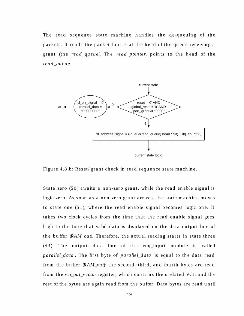
49
The read sequence state machine handles the de-queuing of the
packets. It reads the packet that is at the head of the queue receiving a
grant (the read_queue). The read_pointer, points to the head of the
read_queue.
Figure 4.8.b: Reset/grant check in read sequence state machine.
State zero (S0) awaits a non-zero grant, while the read enable signal is
logic zero. As soon as a non-zero grant arrives, the state machine moves
to state one (S1), where the read enable signal becomes logic one. It
takes two clock cycles from the time that the read enable signal goes
high to the time that valid data is displayed on the data output line of
the buffer (RAM_out). Therefore, the actual reading starts in state three
(S3). The output data line of the voq_input module is called
parallel_data . The first byte of parallel_data is equal to the data read
from the buffer (RAM_out); the second, third, and fourth bytes are read
from the vci_out_vector register, which contains the updated VCI, and the
rest of the bytes are again read from the buffer. Data bytes are read until
reset = '0' ANDglobal_reset = '0' ANDport_grant /= "0000"
current state
current state logic
1
0rd_en_signal = '0'parallel_data =
"00000000"S0
rd_address_signal = ((queue(read_queue).head * 53) + dq_count53)
50
dq_counter53 shows a value of 55 (53 for the bytes in the packet, 2 for
the cycles it took until the buffer output displayed valid data). The state
machine then resets all the signals and clears the dq_counter53 so that
they are ready for the next packet that will be served. The value of the
dq_counter53 is maintained as a temporary signal (dq_count53_temp) for
two clock cycles. This time is required to update the linked lists.
In each state, if there is a valid grant and no reset is active, the read
address signal is assigned an appropriate value. The read address signal
always starts from the first byte of the packet at the head of the read
queue (the queue that is served). The read address signal is incremented
by one after each byte is read. The dq_counter53 counter, counts the
number of bytes that are de-queued and moves the read pointer forward
as the de-queue process continues to read the rest of the packet. In case
of a reset or a zero grant signal from the scheduler, the de-queuing is
disabled and the output data is set to zero.
The read sequence state machine also creates a frame pulse
(data_out_fp), and a data_valid signal for the outgoing data. The out
going frame pulse marks the beginning of the outgoing packet on the
parallel_data_out output line. Similar to the incoming frame pulse, the
first byte of the out going data can be read on the second rising edge of
the clock after the pulse on the data_out_fp line is detected. The data is
only valid when the data_valid signal is high.
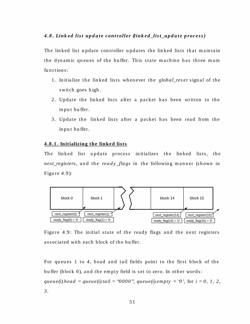
51
4.8. Linked list update controller (linked_list_update process)
The linked list update controller updates the linked lists that maintain
the dynamic queues of the buffer. This state machine has three main
functions:
1. Initialize the linked lists whenever the global_reset signal of the
switch goes high.
2. Update the linked lists after a packet has been written to the
input buffer.
3. Update the linked lists after a packet has been read from the
input buffer.
4.8.1. Initializing the linked lists
The linked list update process initializes the linked lists, the
next_registers, and the ready_flags in the following manner (shown in
Figure 4.9):
Figure 4.9: The initial state of the ready flags and the next registers
associated with each block of the buffer.
For queues 1 to 4, head and tail fields point to the first block of the
buffer (block 0), and the empty field is set to zero. In other words:
queue(i).head = queue(i).tail = “0000”, queue(i).empty = ‘0’, for i = 0, 1, 2,
3.
block 15
next_register(15)
ready_flag(15) = '0'
next_register(14)
ready_flag(14) = '0'
next_register(0)
ready_flag(0) = '0'
next_register(1)
ready_flag(1) = '0'
block 0 block 1 block 14
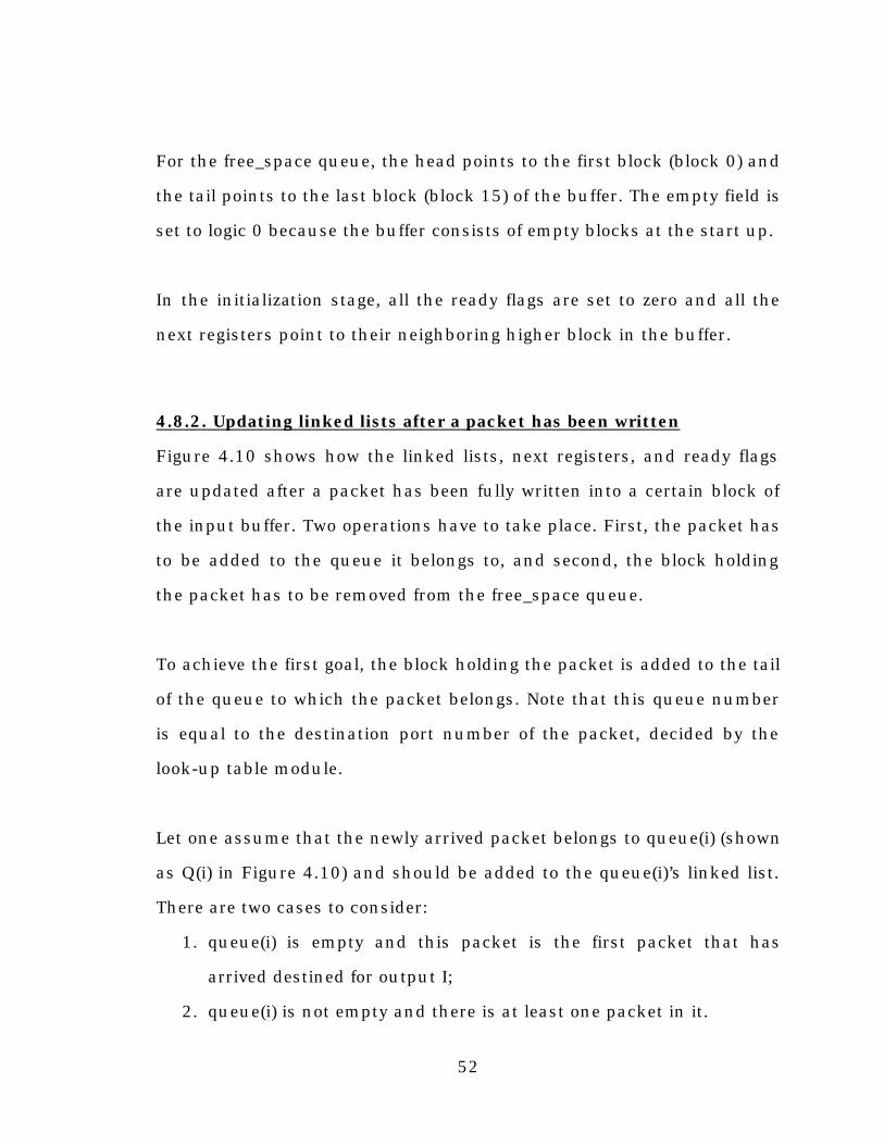
52
For the free_space queue, the head points to the first block (block 0) and
the tail points to the last block (block 15) of the buffer. The empty field is
set to logic 0 because the buffer consists of empty blocks at the start up.
In the initialization stage, all the ready flags are set to zero and all the
next registers point to their neighboring higher block in the buffer.
4.8.2. Updating linked lists after a packet has been written
Figure 4.10 shows how the linked lists, next registers, and ready flags
are updated after a packet has been fully written into a certain block of
the input buffer. Two operations have to take place. First, the packet has
to be added to the queue it belongs to, and second, the block holding
the packet has to be removed from the free_space queue.
To achieve the first goal, the block holding the packet is added to the tail
of the queue to which the packet belongs. Note that this queue number
is equal to the destination port number of the packet, decided by the
look-up table module.
Let one assume that the newly arrived packet belongs to queue(i) (shown
as Q(i) in Figure 4.10) and should be added to the queue(i)’s linked list.
There are two cases to consider:
1. queue(i) is empty and this packet is the first packet that has
arrived destined for output I;
2. queue(i) is not empty and there is at least one packet in it.
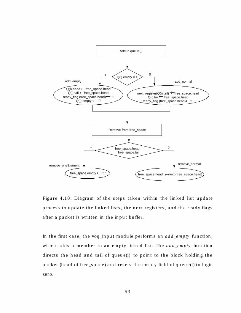
53
Figure 4.10: Diagram of the steps taken within the linked list update
process to update the linked lists, the next registers, and the ready flags
after a packet is written in the input buffer.
In the first case, the voq_input module performs an add_empty function,
which adds a member to an empty linked list. The add_empty function
directs the head and tail of queue(i) to point to the block holding the
packet (head of free_space) and resets the empty field of queue(i) to logic
zero.
Add to queue(i)
Q(i).empty = 1
Q(i).head free_space.headQ(i).tail free_space.head
ready_flag (free_space.head) '1'Q(i).empty '0'
next_register(Q(i).tail) free_space.headQ(i).tail free_space.head
ready_flag (free_space.head) '1'
1 0
add_normaladd_empty
remove_oneElement
free_space.head =free_space.tail
free_space.head next (free_space.head) free_space.empty '1'
remove_normal
01
Remove from free_space
54
In the second case, the add_normal function is performed. This function
assigns the new block as both the new tail of queue(i), and the next
block for the old tail of queue(i).
In both cases the ready_flag associated with the added block is set to
logic 1 to show that the block is not empty and that it is holding a
packet.
Next, the block holding the newly arrived packet has to be removed from
the free_space linked list. Again, there are two cases to consider.
1. The free_space linked list has only one element (i.e., its head and
tail point to the same block);
2. The free_space linked list has more than one element (i.e., its
head and tail are not similar).
In the first case, the remove_oneElement function shown in Figure 4.10
is performed. This function removes the last block from the free_space
linked list by resetting the linked list’s empty field to logic 1.
In the second case, the remove_normal function is performed. This
function removes the new block from the head of the free_space linked
list by making the next block in the list the new head.
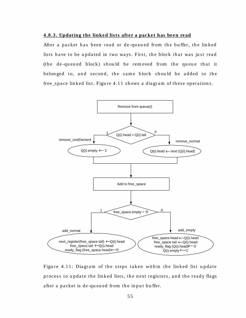
55
4.8.3. Updating the linked lists after a packet has been read
After a packet has been read or de-queued from the buffer, the linked
lists have to be updated in two ways. First, the block that was just read
(the de-queued block) should be removed from the queue that it
belonged to, and second, the same block should be added to the
free_space linked list. Figure 4.11 shows a diagram of these operations.
Figure 4.11: Diagram of the steps taken within the linked list update
process to update the linked lists, the next registers, and the ready flags
after a packet is de-queued from the input buffer.
Remove from queue(i)
Q(i).head = Q(i).tail1 0
add_empty
remove_oneElement
free_space.empty = '0'
Q(i).empty '1'
remove_normal
01
Add to free_space
Q(i).head next (Q(i).head)
free_space.head Q(i).headfree_space.tail Q(i).headready_flag (Q(i).head) '0'
Q(i).empty '1'
next_register(free_space.tail) Q(i).headfree_space.tail Q(i).head
ready_flag (free_space.head) '0'
add_normal
56
Let one assume the de-queued block belongs to queue(i). The procedure
taken here is the same as the last section. The functions performed are
similar only they are performed on different queues. In this case, the
queue being added to is the free_space queue and the queue being
removed from is queue(i).
As shown in Figure 4.11, while removing the packet from queue(i), two
cases can occur: either queue(i) has a single element, in which case the
remove_oneElement function is performed, or it has more than one
element, in which case a remove_normal function takes place.
In the remove_oneElement function the empty field of queue(i) is set to
logic 1, declaring it an empty queue. In the remove_normal function, the
next block to the de-queued block becomes the new head of queue(i).
(Note that packets are removed from the head of the queues.)
To add the removed block to the free_space, the voq_input module
checks whether the free_space linked list is empty. If so, then the
add_empty function shown in Figure 4.11 is performed. This function
points both the head and tail of the free_space linked list to the de-
queued block. It also sets the empty field of the free_space linked list to
zero.
If the free_space queue is not empty, then the de-queued block is added
to the tail of the free_space linked list. The de-queued block becomes
both the new tail of the list, and the next block for the old tail.
57
In both add functions, the ready_flag associated with the de-queued
block is reset to logic 0 to indicate that the new block is empty.
Other than data_valid, parallel_data_out, and data_out_fp signals, the
voq_input module has a 4-bit port_request output connected to the
Scheduler module of the switch. Each bit of the port_request signal
corresponds to a different virtual queue inside the buffer. The request bit
corresponding to a certain queue is logic high, as long as that queue is
not empty.
The VHDL source code for the modules voq_input and LUT are included
in Appendices C.2 and C.5, respectively. The package file used in
voq_input.vhd file is included in Appendix C.7.
58
Chapter 5
The scheduler
There is a centralized scheduler in the 4×4 switch that considers
requests from all the input queues and determines the best realizable
configuration for the crossbar. The scheduler’s decision is determined by
a scheduling algorithm. This scheduling algorithm has to be fast,
efficient, easy to implement in hardware, and fair in serving all the
inputs. There are various scheduling algorithms, some of which were
explained earlier in Chapter 2. The scheduling module (voq_c_bar) in the
4×4 switch uses a crossbar scheduler architecture named Diagonal
Propagation Arbiter (DPA) [11].
DPA is a fair crossbar scheduler with a round robin priority rotation. The
scheduling algorithm is based on a small combinational logic arbiter cell
assigned to each input/output pair. When there is a request to send
packets from a certain input port to a certain output port, the
corresponding arbiter cell receives a request from the input. The arbiter
then issues a grant for the requested output based on both the position
of the priority round robin, and the grants issued to higher priority cells.
For an n×n switch, the maximum arbitration delay through the whole
switch is (n-1)D, where D is a single gate delay. In our switch the
arbitration delay is very small (maximum 4.5 ns) and does not limit the
performance and speed of the switch.
The following sections first describe the basic two dimensional ripple-
carry arbiter, and then the DPA architecture in detail. The basic two
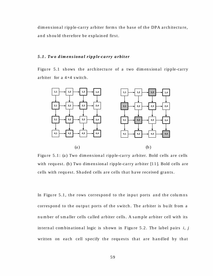
59
dimensional ripple-carry arbiter forms the base of the DPA architecture,
and should therefore be explained first.
5.1. Two dimensional ripple-carry arbiter
Figure 5.1 shows the architecture of a two dimensional ripple-carry
arbiter for a 4×4 switch.
(a) (b)
Figure 5.1: (a) Two dimensional ripple-carry arbiter. Bold cells are cells
with request. (b) Two dimensional ripple-carry arbiter [11]. Bold cells are
cells with request. Shaded cells are cells that have received grants.
In Figure 5.1, the rows correspond to the input ports and the columns
correspond to the output ports of the switch. The arbiter is built from a
number of smaller cells called arbiter cells. A sample arbiter cell with its
internal combinational logic is shown in Figure 5.2. The label pairs i, j
written on each cell specify the requests that are handled by that
1,1 1,2 1,3 1,4
2,1 2,2 2,3 2,4
3,1
4,1
3,2
4,2
3,3
4,3
3,4
4,4
1,1 1,2 1,3 1,4
2,1 2,2 2,3 2,4
3,1
4,1
3,2
4,2
3,3
4,3
3,4
4,4
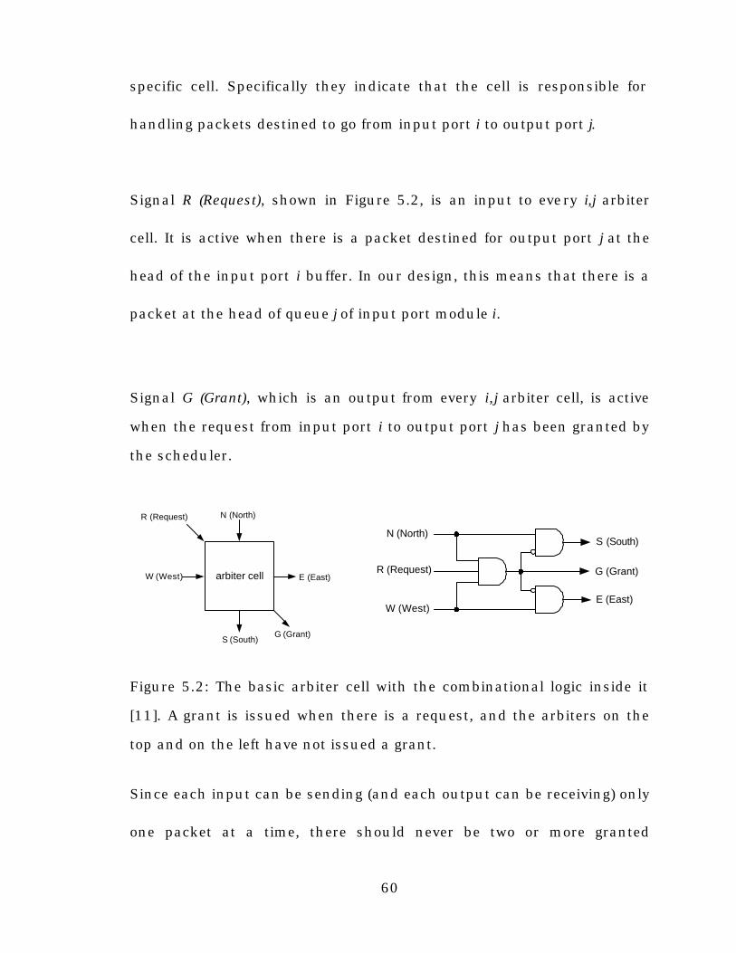
60
specific cell. Specifically they indicate that the cell is responsible for
handling packets destined to go from input port i to output port j.
Signal R (Request), shown in Figure 5.2, is an input to every i,j arbiter
cell. It is active when there is a packet destined for output port j at the
head of the input port i buffer. In our design, this means that there is a
packet at the head of queue j of input port module i.
Signal G (Grant), which is an output from every i,j arbiter cell, is active
when the request from input port i to output port j has been granted by
the scheduler.
Figure 5.2: The basic arbiter cell with the combinational logic inside it
[11]. A grant is issued when there is a request, and the arbiters on the
top and on the left have not issued a grant.
Since each input can be sending (and each output can be receiving) only
one packet at a time, there should never be two or more granted
R (Request)
E (East)W (West) arbiter cell
N (North)
S (South)G (Grant)
N (North)
W (West)
R (Request) G (Grant)
E (East)
S (South)
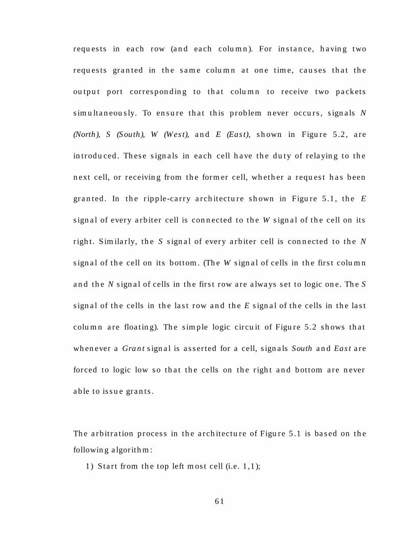
61
requests in each row (and each column). For instance, having two
requests granted in the same column at one time, causes that the
output port corresponding to that column to receive two packets
simultaneously. To ensure that this problem never occurs, signals N
(North), S (South), W (West), and E (East), shown in Figure 5.2, are
introduced. These signals in each cell have the duty of relaying to the
next cell, or receiving from the former cell, whether a request has been
granted. In the ripple-carry architecture shown in Figure 5.1, the E
signal of every arbiter cell is connected to the W signal of the cell on its
right. Similarly, the S signal of every arbiter cell is connected to the N
signal of the cell on its bottom. (The W signal of cells in the first column
and the N signal of cells in the first row are always set to logic one. The S
signal of the cells in the last row and the E signal of the cells in the last
column are floating). The simple logic circuit of Figure 5.2 shows that
whenever a Grant signal is asserted for a cell, signals South and East are
forced to logic low so that the cells on the right and bottom are never
able to issue grants.
The arbitration process in the architecture of Figure 5.1 is based on the
following algorithm:
1) Start from the top left most cell (i.e. 1,1);
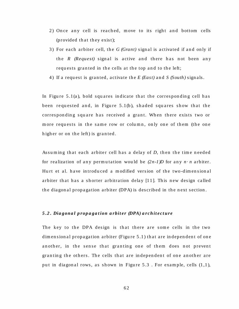
62
2) Once any cell is reached, move to its right and bottom cells
(provided that they exist);
3) For each arbiter cell, the G (Grant) signal is activated if and only if
the R (Request) signal is active and there has not been any
requests granted in the cells at the top and to the left;
4) If a request is granted, activate the E (East) and S (South) signals.
In Figure 5.1(a), bold squares indicate that the corresponding cell has
been requested and, in Figure 5.1(b), shaded squares show that the
corresponding square has received a grant. When there exists two or
more requests in the same row or column, only one of them (the one
higher or on the left) is granted.
Assuming that each arbiter cell has a delay of D, then the time needed
for realization of any permutation would be (2n-1)D for any n×n arbiter.
Hurt et al. have introduced a modified version of the two-dimensional
arbiter that has a shorter arbitration delay [11]. This new design called
the diagonal propagation arbiter (DPA) is described in the next section.
5.2. Diagonal propagation arbiter (DPA) architecture
The key to the DPA design is that there are some cells in the two
dimensional propagation arbiter (Figure 5.1) that are independent of one
another, in the sense that granting one of them does not prevent
granting the others. The cells that are independent of one another are
put in diagonal rows, as shown in Figure 5.3 . For example, cells (1,1),
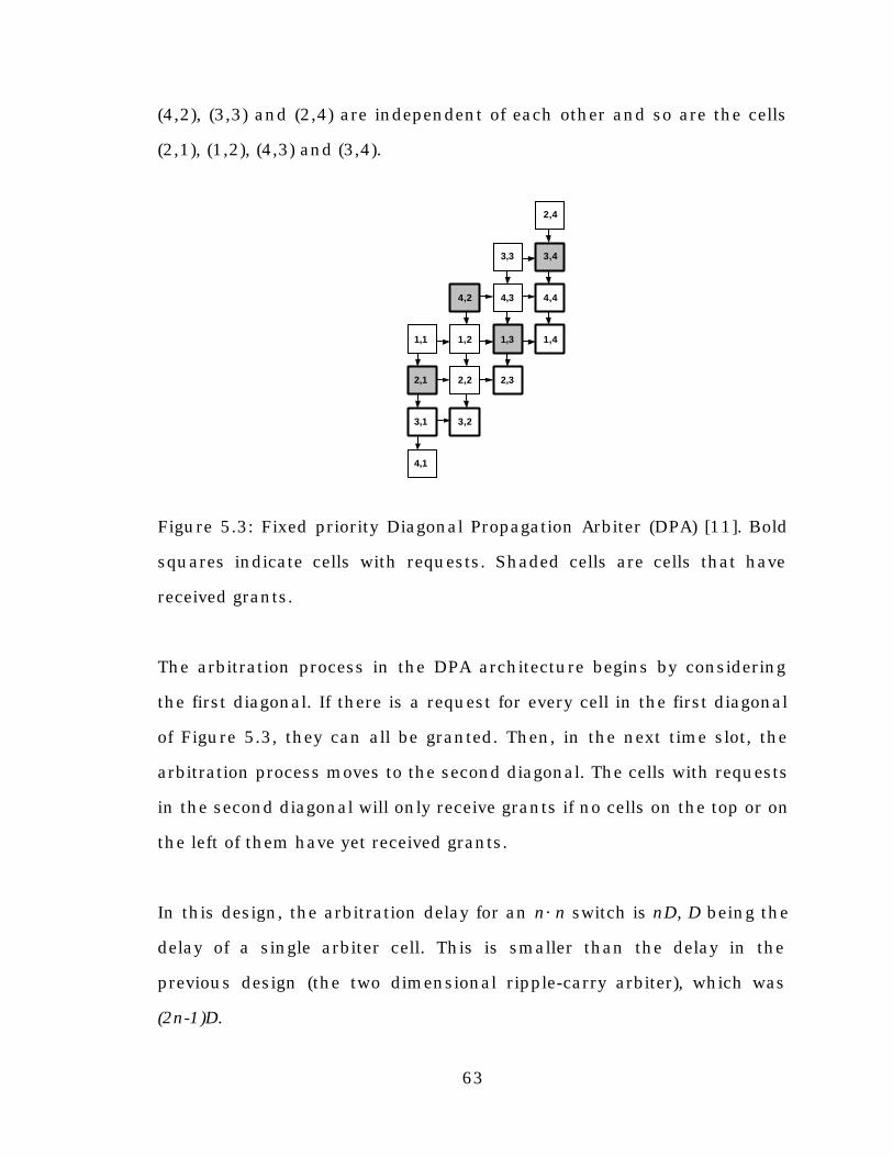
63
(4,2), (3,3) and (2,4) are independent of each other and so are the cells
(2,1), (1,2), (4,3) and (3,4).
Figure 5.3: Fixed priority Diagonal Propagation Arbiter (DPA) [11]. Bold
squares indicate cells with requests. Shaded cells are cells that have
received grants.
The arbitration process in the DPA architecture begins by considering
the first diagonal. If there is a request for every cell in the first diagonal
of Figure 5.3, they can all be granted. Then, in the next time slot, the
arbitration process moves to the second diagonal. The cells with requests
in the second diagonal will only receive grants if no cells on the top or on
the left of them have yet received grants.
In this design, the arbitration delay for an n×n switch is nD, D being the
delay of a single arbiter cell. This is smaller than the delay in the
previous design (the two dimensional ripple-carry arbiter), which was
(2n-1)D.
2,1
1,1
2,1
3,1
4,1
4,2
1,2
2,2
3,2
3,3
4,3
1,3
2,3
2,4
3,4
4,4
1,4
64
One issue that stands out in both ripple-carry and DPA architectures is
the issue of unfairness. The ripple-carry design gives the priority to the
cells that are higher and to the left. Specifically, it gives the highest
priority to cell (1,1). Similarly, in the DPA architecture the highest
priority is always given to the cells in the first diagonal. Therefore, these
two designs are not fair. Optimally one should be able to rotate the
priority so that every cell has the chance of being the highest priority
cell.
One solution to this problem could be to make a cyclic architecture by
connecting the South signals of the cells in the last row (diagonal) to the
North signals of the cells in the first row (diagonal). Similarly, the East
signals of the last column have to be connected to the West signals of the
first column.
Such an architecture would be fair because every cell can have the
opportunity to be the highest priority cell. However, this architecture
suffers from the fundamental problem of having a “combinational
feedback loop”. Such architectures are difficult to design and test; they
are not very well supported by logic synthesis tools and they have to be
carefully simulated at the physical layout level.
To overcome the problems accompanying the cyclic feedback
architecture and to be able to, at the same time, rotate the priorities,
Hurt et al. have found a solution. In this new architecture, shown in
Figure 5.4, the first (n-1) diagonals of an n×n DPA scheduler are repeated
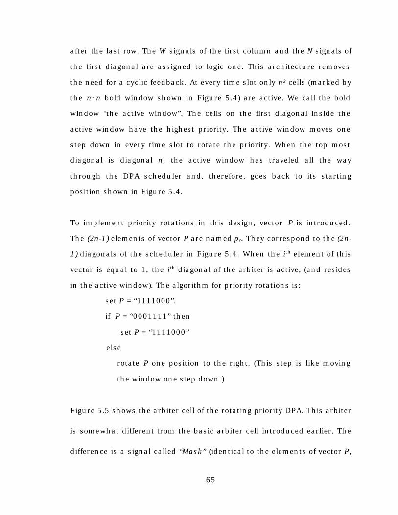
65
after the last row. The W signals of the first column and the N signals of
the first diagonal are assigned to logic one. This architecture removes
the need for a cyclic feedback. At every time slot only n2 cells (marked by
the n×n bold window shown in Figure 5.4) are active. We call the bold
window “the active window”. The cells on the first diagonal inside the
active window have the highest priority. The active window moves one
step down in every time slot to rotate the priority. When the top most
diagonal is diagonal n, the active window has traveled all the way
through the DPA scheduler and, therefore, goes back to its starting
position shown in Figure 5.4.
To implement priority rotations in this design, vector P is introduced.
The (2n-1) elements of vector P are named pr. They correspond to the (2n-
1) diagonals of the scheduler in Figure 5.4. When the ith element of this
vector is equal to 1, the ith diagonal of the arbiter is active, (and resides
in the active window). The algorithm for priority rotations is:
set P = “1111000”.
if P = “0001111” then
set P = “1111000”
else
rotate P one position to the right. (This step is like moving
the window one step down.)
Figure 5.5 shows the arbiter cell of the rotating priority DPA. This arbiter
is somewhat different from the basic arbiter cell introduced earlier. The
difference is a signal called “Mask” (identical to the elements of vector P,
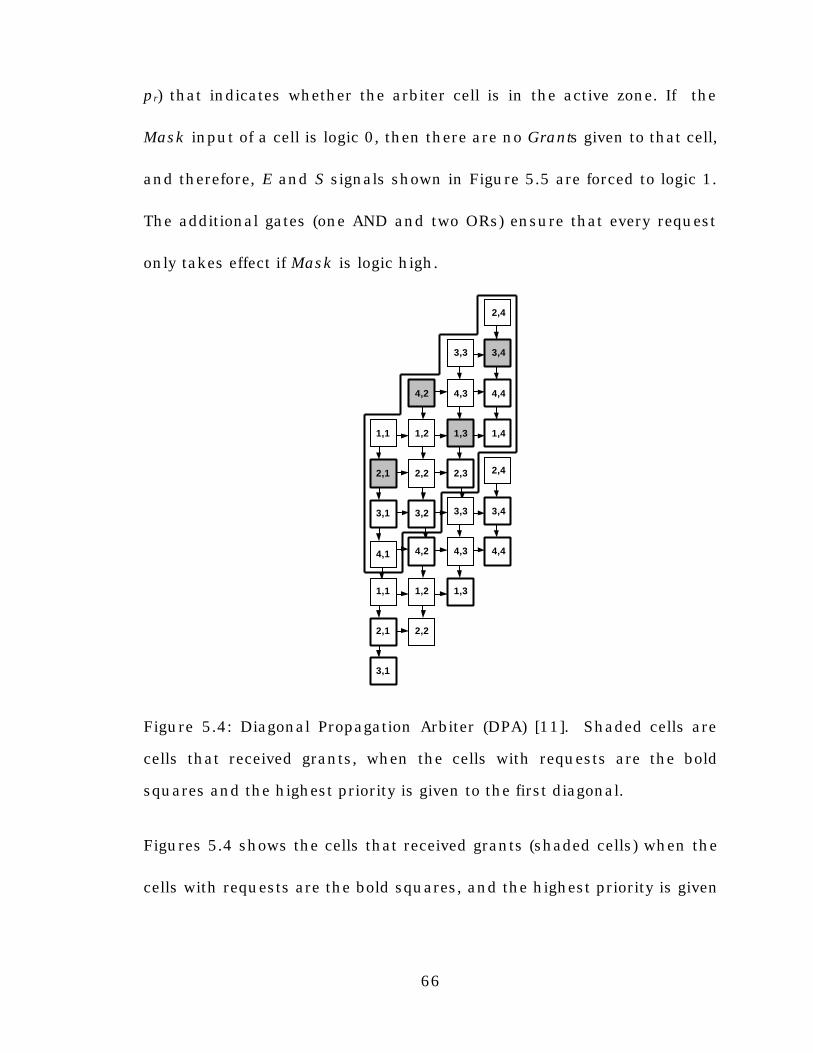
66
pr) that indicates whether the arbiter cell is in the active zone. If the
Mask input of a cell is logic 0, then there are no Grants given to that cell,
and therefore, E and S signals shown in Figure 5.5 are forced to logic 1.
The additional gates (one AND and two ORs) ensure that every request
only takes effect if Mask is logic high.
Figure 5.4: Diagonal Propagation Arbiter (DPA) [11]. Shaded cells are
cells that received grants, when the cells with requests are the bold
squares and the highest priority is given to the first diagonal.
Figures 5.4 shows the cells that received grants (shaded cells) when the
cells with requests are the bold squares, and the highest priority is given
2,1
1,1
2,1
3,1
4,1
4,2
1,2
2,2
3,2
3,3
4,3
1,3
2,3
2,4
3,4
4,4
1,4
2,12,1
3,1
1,2
2,2
4,3
1,3
2,4
3,4
4,4
1,1
3,3
4,2
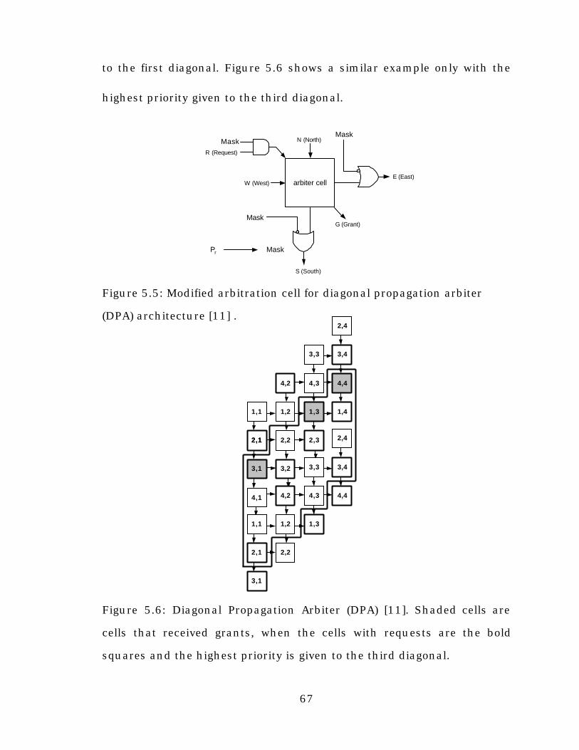
67
to the first diagonal. Figure 5.6 shows a similar example only with the
highest priority given to the third diagonal.
Figure 5.5: Modified arbitration cell for diagonal propagation arbiter
(DPA) architecture [11] .
Figure 5.6: Diagonal Propagation Arbiter (DPA) [11]. Shaded cells are
cells that received grants, when the cells with requests are the bold
squares and the highest priority is given to the third diagonal.
R (Request)
E (East)W (West) arbiter cell
N (North)
S (South)
G (Grant)Mask
MaskMask
Pr Mask
2,1
1,1
2,1
3,1
4,1
4,2
1,2
2,2
3,2
3,3
4,3
1,3
2,3
2,4
3,4
4,4
1,4
2,12,1
3,1
1,2
2,2
4,3
1,3
2,4
3,4
4,4
1,1
3,3
4,2
68
The input to the scheduler block in our switch is a 16 bit vector. The
elements of this vector correspond to the 16 possible requests in a 4×4
switch. This input vector is constructed from the request lines that come
from each input port module. The output of the scheduler is also a 16 bit
vector. This vector's elements are the grants issued by the scheduler.
This array constructs the control lines of the fabric.
In our voq_c_bar module, the priority vector P rotates on the rising edge
of the c_bar_clock (the internal clock with the period of a packet time).
The requests coming from the input port modules are also sent to the
scheduler on the rising edge of the c_bar_clock. Therefore, for a whole
packet time, the request and grant signals remain constant and a whole
packet is de-queued from the input buffers.
Appendix C.3 contains the VHDL source code for the voq_c_bar module.
69
Chapter 6
The fabric
The crossbar fabric module in the design (shown in figure 6.1) is
responsible for physically connecting an input port to its destined
output port, based on the grants issued by the scheduler. The inputs of
voq_fabric (except for the cntrl input) are connected to the input port
modules of our switch. The outputs of voq_fabric are connected to the
output ports of the switch. The fabric makes the appropriate connection
between each input and its corresponding output.
Figure 6.1: Crossbar fabric module in our switch is the physical
connection between the input and output ports of the switch.
The signals going through the fabric are: data bytes, frame pulse signals,
data_valid signals, and the two-bit input port numbers. Each input to
voq_fabric (except for input_data and cntrl) is a 4-bit wide signal, where
input_data
input_fp
input_data_valid
"1100"
"1010" port_name_bit0
cntrl
4x8
voq_fabric4
4
4
4
4
16
output_data
output_fp
output_data_valid
port_name_bit1
4x8
4
4
4
70
each bit comes from a different input port module. For example, in case
of the 4-bit input_fp input of voq_fabric, input_fp(0) comes from input
port module 1, input_fp(1) comes from input port module 2, et cetera.
The input_data input of voq_fabric however, consists of 4 parallel “bytes”,
rather than bits. Similarly, each byte comes from a different input port
module. The cntrl input of voq_fabric is 16 bits wide and is connected to
the grant output signal of the scheduler. This cntrl signal configures the
fabric and makes the necessary connections. This is described in more
detail later.
Imagine a 4×4 crossbar similar to the one shown in Figure 6.2. Every
four bit input signal of the voq_fabric module passes through a similar
crossbar. In each crossbar, the 4 horizontal buses (rows) are connected
to the 4 bits of a certain input of the voq_fabric. Similarly, the 4 vertical
buses (columns) of the crossbar are connected to the 4 bits of a certain
voq_fabric output. For example input_fp(0) is connected to the first input
of a certain crossbar, input_fp(1) is connected to the second input of the
same crossbar, et cetera. Therefore, ignoring the input_data input for a
moment, four copies of the crossbar are needed for the other four inputs
of voq_fabric. Since input_data is a 4×8 bit input signal, it requires eight
copies of such a crossbar. Therefore, in the voq_fabric module, a sum of
twelve crossbars pass the eight bit data bytes and the other four inputs .
In every crossbar the cross points are controlled by the cntrl input of the
voq_fabric module (Figure 6.3). Each bit of the cntrl input corresponds to
one of the cross points of the crossbar. If a certain cntrl bit is logic high,
then the corresponding cross point is closed. The inputi and outputi
71
signals, shown in Figure 6.3, stand for the inputs and outputs of
voq_fabric.
Figure 6.2: A 4×4 crossbar. The horizontal lines are connected to the
inputs and the vertical lines are connected to the outputs of the
voq_fabric module.
Figure 6.3: Crossbar for the voq_fabric module. Each bit of cntrl input
corresponds to a certain cross point in the crossbar.
inputi(0)
inputi(1)
outp
uti(0
)
outp
uti(1
)
outp
uti(2
)
outp
uti(3
)
inputi(2)
inputi(3)
cntrl(0) cntrl(1) cntrl(2) cntrl(3)
cntrl(4) cntrl(5)
cntrl(14)
cntrl(7)
cntrl(8) cntrl(9) cntrl(10) cntrl(11)
cntrl(12) cntrl(13)
cntrl(6)
cntrl(15)
72
The diagram of Figure 6.3 performs the following procedure: Each bit of
the output is the logical sum (OR) of inputi’s bits 0 to 3 AND’d with the
cntrl lines in that output bit’s column. For example (see Figures 6.4 and
6.5),
output_fp(2) = [ ( input_fp(0) AND cntrl(2) ) OR (input_fp(1) AND cntrl(6) ) OR
(input_fp(2) AND cntrl(10) ) OR (input_fp(3) AND cntrl(14) ) ]
Figure 6.4: The output_fp(2) is the logical sum of input_fp bits AND’d with
corresponding cntrl bits.
Figure 6.5 shows the 12 crossbars in the voq_fabric module. One copy of
the crossbar is needed to connect the frame pulse lines from the input
port modules to the output ports of the switch. Another copy of the
crossbar is used for data_valid signals. In order to connect the outgoing
data bytes from the input port modules to the data_out_port lines of the
switch, 8 copies of the crossbar are used. Finally, two copies of the
input_fp(1)
output_fp(2)
input_fp(2)
input_fp(3)
cntrl(14)
cntrl(10)
cntrl(6)
input_fp(0)
cntrl(2)
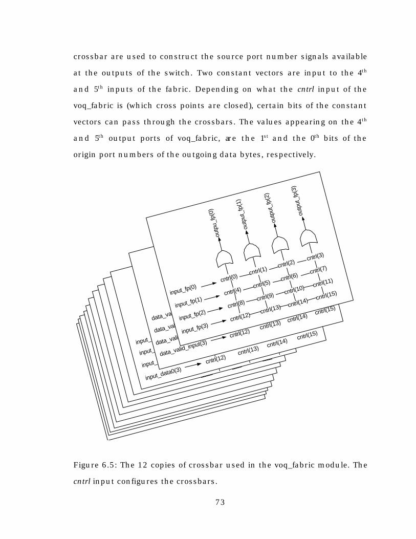
73
crossbar are used to construct the source port number signals available
at the outputs of the switch. Two constant vectors are input to the 4th
and 5th inputs of the fabric. Depending on what the cntrl input of the
voq_fabric is (which cross points are closed), certain bits of the constant
vectors can pass through the crossbars. The values appearing on the 4th
and 5th output ports of voq_fabric, are the 1st and the 0th bits of the
origin port numbers of the outgoing data bytes, respectively.
Figure 6.5: The 12 copies of crossbar used in the voq_fabric module. The
cntrl input configures the crossbars.
outp
uti(0
)
outp
uti(1
)
outp
uti(2
)
outp
uti(3
)
cntrl(0)cntrl(1)
cntrl(2)cntrl(3)
cntrl(5)
cntrl(7)
cntrl(11)cntrl(6)
outp
uti(0
)
outp
uti(1
)
outp
uti(2
)
outp
uti(3
)
cntrl(0)cntrl(1)
cntrl(2)cntrl(3)
cntrl(7)
cntrl(11)cntrl(6)
outp
ut_f
p(3)
input_data0(0)
input_data0(1)
input_data0(2)
input_data0(3)
cntrl(4)
cntrl(14)cntrl(8)
cntrl(9)cntrl(10)
cntrl(12)cntrl(13)
cntrl(15)
data_valid_input(0)
data_valid_input(1)
data_valid_input(2)
data_valid_input(3)
cntrl(4)cntrl(5)
cntrl(14)cntrl(8)
cntrl(9) cntrl(10)
cntrl(12) cntrl(13)
cntrl(15)
input_fp(0)
input_fp(1)
outp
u_fp
(0)
outp
ut_f
p(1)
outp
ut_f
p(2)
input_fp(2)
input_fp(3)
cntrl(0) cntrl(1) cntrl(2) cntrl(3)
cntrl(4) cntrl(5)
cntrl(14)
cntrl(7)
cntrl(8) cntrl(9) cntrl(10) cntrl(11)
cntrl(12) cntrl(13)
cntrl(6)
cntrl(15)ou
tput
_fp(
3)
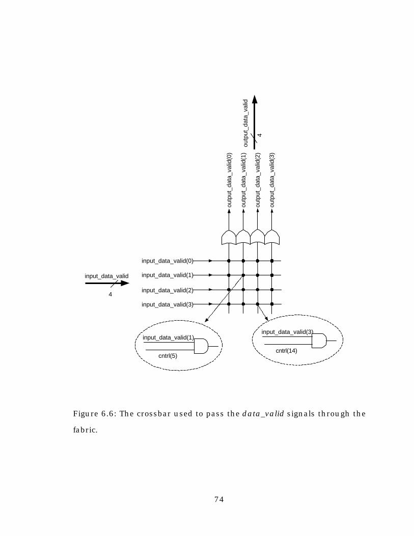
74
Figure 6.6: The crossbar used to pass the data_valid signals through the
fabric.
input_data_valid
input_data_valid(0)
input_data_valid(1)
4
outp
ut_d
ata_
valid
(0)
outp
ut_d
ata_
valid
4
input_data_valid(2)
input_data_valid(3)
outp
ut_d
ata_
valid
(1)
outp
ut_d
ata_
valid
(2)
outp
ut_d
ata_
valid
(3)
input_data_valid(1)
cntrl(5)
input_data_valid(3)
cntrl(14)
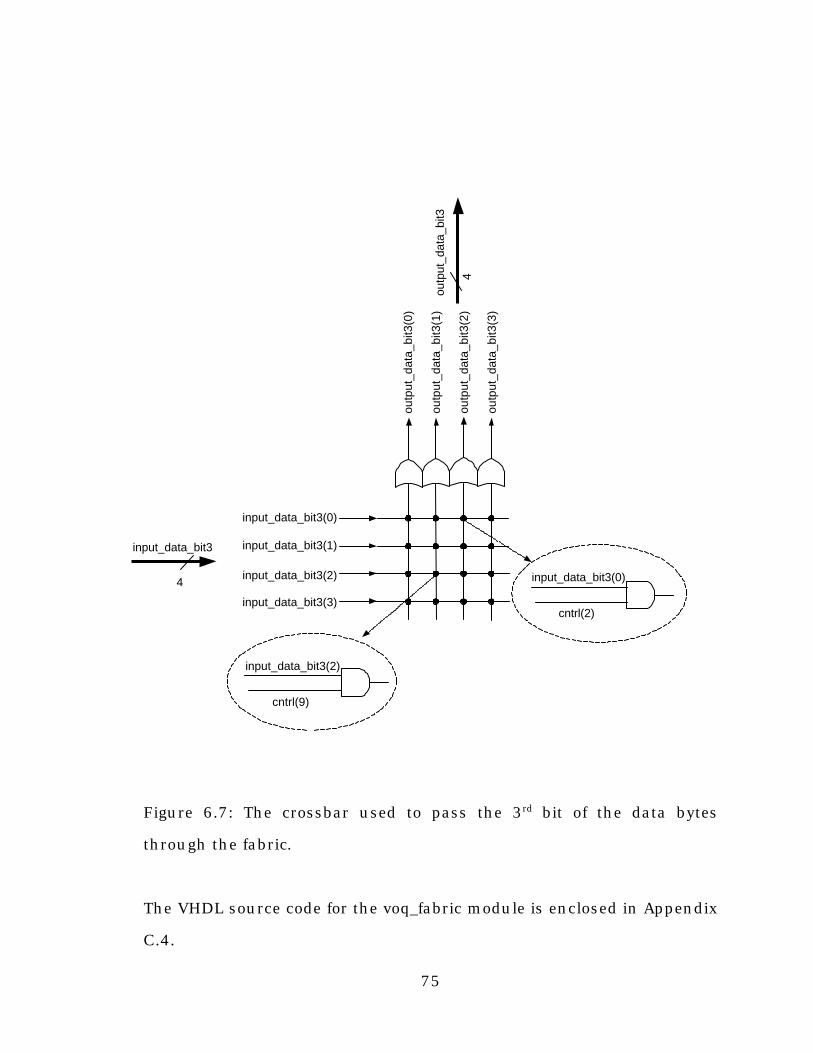
75
Figure 6.7: The crossbar used to pass the 3rd bit of the data bytes
through the fabric.
The VHDL source code for the voq_fabric module is enclosed in Appendix
C.4.
input_data_bit3
input_data_bit3(0)
input_data_bit3(1)
4
outp
ut_d
ata_
bit3
(0)
outp
ut_d
ata_
bit3
4
input_data_bit3(2)
input_data_bit3(3)
outp
ut_d
ata_
bit3
(1)
outp
ut_d
ata_
bit3
(2)
outp
ut_d
ata_
bit3
(3)
input_data_bit3(0)
cntrl(2)
input_data_bit3(2)
cntrl(9)
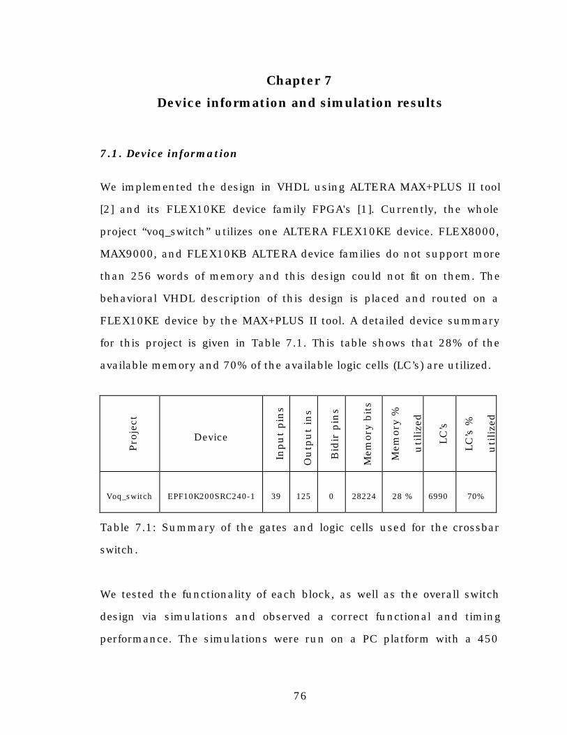
76
Chapter 7
Device information and simulation results
7.1. Device information
We implemented the design in VHDL using ALTERA MAX+PLUS II tool
[2] and its FLEX10KE device family FPGA's [1]. Currently, the whole
project “voq_switch” utilizes one ALTERA FLEX10KE device. FLEX8000,
MAX9000, and FLEX10KB ALTERA device families do not support more
than 256 words of memory and this design could not fit on them. The
behavioral VHDL description of this design is placed and routed on a
FLEX10KE device by the MAX+PLUS II tool. A detailed device summary
for this project is given in Table 7.1. This table shows that 28% of the
available memory and 70% of the available logic cells (LC’s) are utilized.
Pro
ject
Device
Inpu
t pin
s
Ou
tpu
t in
s
Bid
ir p
ins
Mem
ory
bit
s
Mem
ory
%
uti
lize
d
LC’s
LC’s
%
uti
lize
d Voq_switch EPF10K200SRC240-1 39 125 0 28224 28 % 6990 70%
Table 7.1: Summary of the gates and logic cells used for the crossbar
switch.
We tested the functionality of each block, as well as the overall switch
design via simulations and observed a correct functional and timing
performance. The simulations were run on a PC platform with a 450
77
MHz Pentium III processor and a Windows NT operating system. The
compilation time for the overall switch lasted two hours.
The maximum achieved clock rate for this design on the
EPF10K200SRC240-1 device is 16.6 MHz. The Timing Analyzer tool in
MAX+PLUS II calculates this value based on the longest path in the
design. On a different device, the clock rate could be either larger or
smaller, depending on the device technology and the way MAX+PLUS II
places and routes the design on the device. (FLEX10KE has a 0.22
micron CMOS technology). Pipelining, i.e., dividing the switch data path
to multiple sections and connecting a separate clock input to each, can
also increase the highest achievable clock rate.
We ran the simulations for 300 µsec and observed that the switch is
capable of switching 4 input lines at the rate of 132.8 Mbps into 4
output lines at the same rate. The packets are successfully routed and
sent out of the switch. Eight bits of data are input to the switch at every
clock cycle, and hence the line rate of 132.8 Mpbs is resulted from a
16.6 MHz clock. It takes 53 clock cycles (3.18 µsec) for a single ATM
packet to enter the switch and in our 300 µsec simulations close to 95
packets were input. The simulations lasted a couple of minutes in real
time.
The traffic applied to this switch was a constant bit rate traffic with
uniform distribution over all the input ports. The switch was not tested
for other traffic types. The output data stream and the performance of
the switch would be different for non-constant traffic distributions. For
78
instance, the buffers would have a higher overflow probability for traffic
that occurs in bursts. Furthermore, cells entering the switch in a burst
and destined for a common output can be delayed in the switch and can
leave the switch with longer inter-packet times, due to the priority
rotations in the fair round robin scheduler module.
7.2. Simulation results
We tested the functionality of every component in the switch via
simulations. The simulation results are shown in Appendix D. The
following sections give a detailed explanation of the simulation results.
7.2.1. Simulation results of the switch (Appendix D.1)
Appendix D.1 shows the results of a certain simulation of the switch that
was run for 75 µsec (longer simulations were run as well, but have not
been included in this document). Appendix D.1 shows a two-page
overview of what is happening in this simulation.
In Appendix D.1, one notes that 9 packets are input to every data input
of the switch (there are 9 frame pulses on the input fp lines). On the
data_out_port lines these packets are seen coming out of the output
ports. The simulation data going to all of the inputs is the same, but
according to the position of the priority round robin in the scheduler,
only certain inputs are allowed to send their packet to their desired
output port at any given time. For every packet, the origin port number
(incoming_port_to_output) is output as well. Note that data on the output
ports is only valid if the corresponding data_valid line is high. Also, note
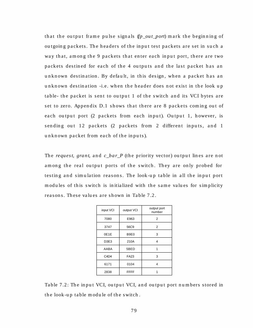
79
that the output frame pulse signals (fp_out_port) mark the beginning of
outgoing packets. The headers of the input test packets are set in such a
way that, among the 9 packets that enter each input port, there are two
packets destined for each of the 4 outputs and the last packet has an
unknown destination. By default, in this design, when a packet has an
unknown destination -i.e. when the header does not exist in the look up
table- the packet is sent to output 1 of the switch and its VCI bytes are
set to zero. Appendix D.1 shows that there are 8 packets coming out of
each output port (2 packets from each input). Output 1, however, is
sending out 12 packets (2 packets from 2 different inputs, and 1
unknown packet from each of the inputs).
The request, grant, and c_bar_P (the priority vector) output lines are not
among the real output ports of the switch. They are only probed for
testing and simulation reasons. The look-up table in all the input port
modules of this switch is initialized with the same values for simplicity
reasons. These values are shown in Table 7.2.
Table 7.2: The input VCI, output VCI, and output port numbers stored in
the look-up table module of the switch.
input VCI output VCI output portnumber
7080
3747
0E1E
D3E3
AABA
C4D4
6171
2838
E963
56C9
B9E0
210A
5BED
FA23
0104
FFFF
2
2
3
4
1
3
4
1
80
As described in earlier chapters, the switch has an internal clock that
runs 59 times slower than the input clock. The period of this internal
clock is actually equal to a packet time. At the rising edge of this clock,
the priority vector is shifted in the crossbar scheduler and also a request
is sent out from the input port modules to the scheduler.
Table 7.3 provides a summary of the simulation results of Appendix D.1.
We have filled the first 6 columns of this table with the input data, and
have predicted the values of certain signals, registers and output ports,
in the rest of the columns. Later, these parameters were compared with
the simulation results and equal values were observed.
Every packet coming to the data input ports of the switch is shown on a
separate line in Table 7.3. There are 9 packets arriving at the input ports
one after the other. For every arriving packet we have shown the first
four bytes, and the last byte. The second, third, and fourth bytes of the
packet are stored in the vci_in_vector register. Bits 4 to 19 of this vector
contain the VCI information of the packet. This VCI value is searched in
the look-up table (shown in Table 7.2) and the output VCI, together with
the output port number, is determined. The output_vci value replaces the
input_vci part (bits 4 to 19) of the vci_in_vector and is stored in the
vci_out_vector register. When the packet is being sent out from the
destination output port, the bytes of vci_out_vector are sent out in place
of bytes 2, 3, and 4 of the packet. This effect is shown in the last
columns of the table, where the first four and the last byte of the
outgoing packet are shown. Note that for the last packet, because the
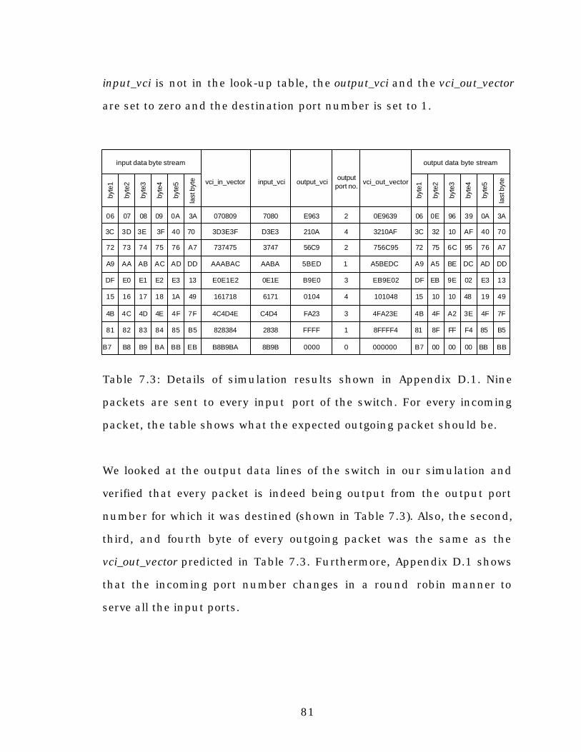
81
input_vci is not in the look-up table, the output_vci and the vci_out_vector
are set to zero and the destination port number is set to 1.
Table 7.3: Details of simulation results shown in Appendix D.1. Nine
packets are sent to every input port of the switch. For every incoming
packet, the table shows what the expected outgoing packet should be.
We looked at the output data lines of the switch in our simulation and
verified that every packet is indeed being output from the output port
number for which it was destined (shown in Table 7.3). Also, the second,
third, and fourth byte of every outgoing packet was the same as the
vci_out_vector predicted in Table 7.3. Furthermore, Appendix D.1 shows
that the incoming port number changes in a round robin manner to
serve all the input ports.
70
72 A773
vci_in_vector input_vci output_vcioutput
port no.vci_out_vector
byte
1
byte
2
byte
3
byte
4
byte
5
last
byt
e
input data byte stream
byte
1
byte
2
byte
3
byte
4
byte
5
last
byt
e
output data byte stream
0607 08 09 0A 3A 070809 7080 E963 2 0E9639 0E 96 39 0A 3A06
3C 3D 3E 3F 40 70 3D3E3F D3E3 210A 4 3210AF 3C 32 10 AF 40
74 75 76 A7 737475 3747 56C9 2 756C95 72 75 6C 95 76
A9 AA AB AC AD DD AAABAC AABA 5BED 1 A5BEDC A9 A5 BE DC AD DD
DF E0 E1 E2 E3 13 E0E1E2 0E1E B9E0 3 EB9E02 DF EB 9E 02 E3 13
15 16 17 18 1A 49 161718 6171 0104 4 101048 15 10 10 48 19 49
4B 4C 4D 4E 4F 7F 4C4D4E C4D4 FA23 3 4FA23E 4B 4F A2 3E 4F 7F
81 82 83 84 85 B5 828384 2838 FFFF 1 8FFFF4 81 8F FF F4 85 B5
B7 B8 B9 BA BB EB B8B9BA 8B9B 0000 0 000000 B7 00 00 00 BB BB
82
7.2.2. Simulation results of the input port module (Appendix D.2)
We tested the functionality of all the components of the switch via
extensive simulations. As an example, Appendix D.2 shows the
simulation results for the “voq_input” module of the switch. Some
internal signals are also probed here for testing and validation purposes.
The values of the linked lists, next registers, read/write addresses,
counter values, enable signals, state variables, et cetera., are some
examples of such internal signals. The accurate performance of the
input module state machines discussed earlier in Chapter 3 was verified,
based on the value of these signals. Note that the destination port
number runs from 0 to 3 to indicate output ports 1 to 4.
This simulation, also tested the voq_input module for overflow. We
disable the de-queue process -by not providing any nonzero grant
inputs- and see that after 16 packets arrive, the input module does not
write any more packets into the buffer. The packets that arrive at the
input ports after the buffer is full are simply dropped. The overflow
occurs at around 75 µsec (in this simulation) when the last packet is
written. Since no grant is issued, no packet is de-queued and therefore
the buffer is filled and all the ready_flags are high.
83
Conclusion and future work
This thesis project, used a hardware description language called VHDL
to implement a 4×4 ATM crossbar switch.
The 4×4 switch designed herein has three modules: “voq_input”,
“voq_c_bar”, and “voq_fabric”. The voq_input module employs an existing
algorithm called virtual output queuing (VOQ). The design of this module
and the queue management scheme was described in Chapter 4. The
voq_c_bar module discussed in Chapter 5 is a fair scheduler with an
architecture called “diagonal propagation arbiter” (DPA). The voq_fabric
module comprises the crossbar fabric of our switch and provides the
physical connection between the inputs and outputs of the switch. The
voq_fabric module was outlined in Chapter 6.
The contributions of this project are:
� A novel design and VHDL implementation of an input port module
employing the VOQ algorithm;
� VHDL implementation of the DPA algorithm;
� A novel design and VHDL implementation of a crossbar fabric;
� A novel composition of the modules into a 4×4 ATM witch and VHDL
implementation of it.
This design implementation entailed the employment of MAX+PLUS II
software tool from ALTERA. Upon testing the functionality of the switch
through simulations, satisfactory functional and timing performances
were observed. The switch functions at a line rate of 132.8 Mbps with a
84
maximum clock frequency of 16.6 MHZ. This design can fit on a single
FLEX10KE ALTERA chip.
I started this project together with Arash Haidari. We designed an 8×8
version of the scheduler, a fabric that handled serial bits, and input port
modules with FIFO queues [10]. Our design could fit on 6 FLEX10KE
FPGA’s, partly due to large pin numbers. Later, I designed an output
port module for the 8×8 switch (presented in Appendix B), which is not
included in the current switch design.
I made further additions and improvements to the design. I designed a
new input port module that employs VOQ’s to prevent head of line (HOL)
blocking. In order to achieve higher line rates in the new input port
module, input data is in the form of parallel bytes (rather than serial
bits). I also designed a new fabric that handles parallel data bytes. I
scaled the design down to 4×4 because the compilation time for the
overall design was too long (over 3 hours). The compilation time for the
4×4 switch is roughly the same, however four dynamic queues with their
linked list logic have been added to each input port. An 8×8 switch with
eight dynamic queues in each input port would have been a much
bigger design and would have resulted in even higher compilation times.
One future plan for this project is to design output port modules with
congestion control, policing, or priority mechanisms. An ATM switch
should not send its packets out to the network unless there is consent
from the down stream nodes. Otherwise congestion can occur in the
network, or packets can be dropped due to buffer overflow at the
85
destination node. Implementation of algorithms that would handle the
communication between the network and the switch is mainly done in
output port modules. For example, a window based flow control design at
the output port module can prevent bursts of data from entering the
network. Implementation of such algorithms in an output port module is
the next step for this project.
Implementing the design on an ALTERA FLEX10KE chip and hardware
testing and verification of the switch is another future plan. Finally,
simulation and synthesis with Synopsys tools, gate level design, layout
and manufacturing of the switch chip could be done.
86
References
[1] ALTERA FLEX 10KE devices:
http://www.altera.com/html/products/f10ke.html
[2] ALTERA MAX+PLUS II software,
http://www.altera.com/html/tools/maxplus.html
[3] T. E. Anderson, S. S. Owicki, J. B. Saxe, and C. P. Thacker, “High
speed switch scheduling for local area networks,” ACM Transactions on
Computer Systems, pp. 319-352, November 1993.
[4] M. Chen and N. D. Georganas, “A fast algorithm for multi-
channel/port traffic scheduling,” Proc. IEEE Supercom/ICC ’94, New
Orleans, Louisiana, May 1994, pp. 96-100.
[5] H. S. Chi and Y. Tamir, “Decomposed arbiters for large crossbars with
multi-queue input buffers,” Proc. of International Conference on
Computer Design, Cambridge, Massachusetts, October 1991, pp. 233-
238.
[6] S. T. Chuang, A. Goel, N. McKeown, and B. Prabhakar, “Matching
output queuing with a combined input output queued switch,” Computer
Systems Technical Report CSL-TR-98-758, March 1998.
87
[7] J. Duato, S. Yalamanchili, and L. Ni, Interconnection Networks: An
Engineering Approach, Los Alamitos, CA: IEEE Computer Society Press,
1997, pp. 17-28.
[8] ForeRunner ASX-200:
http://www.marconi.com/html/solutions/asx200bxasx1000andasx1200
.htm
[9] J. Giacopelli, J. Hickey, W. Marcus, W. Sincoskie, and M. Littlewood,
“Sunshine: A high-performance self routing broadband packet switch
architecture,” IEEE Journal on Selected Areas in Communications, vol. 9,
no. 8, pp.1289-1298, October 1991.
[10] A. Haidari-Khabbaz, “Hardware implementation of a high-speed
crossbar switch,” B.A.Sc. Thesis, Simon Fraser University, Burnaby,
November 2000.
[11] J. Hurt, A. May, X. Zhu, and B. Lin, “Design and implementation of
high-speed symmetric crossbar schedulers,” Proc. IEEE International
Conference on Communications (ICC’99), Vancouver, Canada, June 1999,
pp. 253-258.
[12] M. J. Karol, M. G. Hluchyj, and S. P. Morgan, “Input versus output
queuing on a space-division packet switch,” IEEE Transactions on
Communication, vol. COM-35, no. 12, pp. 1347-1356, December 1987.
[13] M. Katevenis, D. Serpanos, and P. Vatsolaki, “ATLAS I: A General-
Purpose, Single-Chip ATM Switch with Credit-Based Flow Control”, Proc.
88
of the Hot Interconnects IV Symposium, Palo Alto, California, August 1996,
pp. 63-73
[14] S. Keshav, An Engineering Approach to Computer Networking.
Reading, MA: Addison Wesley, January 1998, pp. 47-64.
[15] N. McKeown, “The iSLIP scheduling algorithm for input-queued
switches,” IEEE Transactions on Networking, vol. 7, no. 2, pp. 188-201,
April 1999.
[16] N. McKeown, V. Anamtharam, and J. Warland, “Achieving 100%
throughput in an input-queued switch,” Proc. INFOCOM’96, San
Francisco, March 1996, pp. 296-302.
[17] N. McKeown and T. E. Anderson, “A quantitative comparison of
scheduling algorithms for input-queued switches," Computer Networks
and ISDN Systems, vol. 30, no. 24, pp. 2309-2326, Dec. 1998.
[18] N. McKeown, M. Izzard, A. Mekkittikul, B. Ellersick, and M.
Horowitz, “The Tiny Tera: A small, high bandwidth network switch,” IEEE
Micro, January/February 1997, pp. 26-33.
[19] N. McKeown, P. Varaiya, J. Warland, “Scheduling cells in an input-
queued switch,” Electronic Letters, no. 25, pp. 2174-2175, Dec. 1993.
89
[20] A. Mekkittikul and N. McKeown, “A practical scheduling algorithm
to achieve 100% throughput in input-queued switches,” Proc. IEEE
INFOCOM 1998, vol. 2, Apr. 1998, San Francisco, pp. 792-799.
[21] A. Mekkittikul and N. McKeown, “A starvation-free algorithm for
achieving 100% throughput in an input-queued switch,” Proc. ICCCN’96,
Washington D.C., October 1996, pp. 226-231.
[22] Y. Tamir and H.C. Chi, “Symmetric crossbar arbiters for VLSI
communication switches,” IEEE Transactions on Parallel and Distributed
Systems, vol. 4, no. 1, pp. 13-27, January 1993.
[23] Y. Tamir and G. L. Frazier, “Dynamically-allocated multi-queue
buffers for VLSI communication switches,” IEEE Transactions on
Computers, vol. 41, no. 6, pp. 725-737, June 1992.
[24] F. A. Tobagi, “Fast packet switch architectures for broadband
integrated services digital networks,” Proc. of the IEEE, vol. 78, January
1990, pp. 133-178.
[25] J. Turner and N. Yamanaka, “Architectural choices in large scale
ATM switches,” IEICE Transactions in Communications, vol. E81-B, no. 2,
pp.120-137, February 1998.
[26] Y. Yeh, M.G. Hluchyj, and A. S. Acampora “The knockout switch: A
simple, modular architecure for high-performance packet switching,”
90
IEEE Journal on Selected Areas in Communications, vol. SAC-5, no. 8,
Oct. 1987.
[27] E. W. Zegura, “Architectures for ATM switching systems,” IEEE
Communications Magazine, pp. 28-37, Feb. 1993.
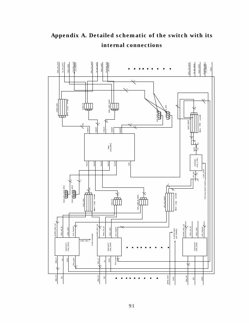
91
Appendix A. Detailed schematic of the switch with its
internal connections
4
Por
t_gr
ant
Por
t_gr
ant
fp
data
_in
para
llel_
data
_out
dat
a_ou
t_fp
data
_val
idin
put p
ort 1
(voq
_inp
ut)
p
ort_
requ
est
fp
data
_in
inpu
t por
t 2(v
oq_i
nput
)
inpu
t_fp
data
_val
id_t
o_fa
bric
fabr
ic(v
oq_f
abric
)
gran
t_si
gnal
sche
dule
r(v
oq_c
_bar
)
arb_
req
gran
t
arb_
req_
sign
al1100
1010
inpu
t_po
rt_n
ame_
bits
1
inpu
t_po
rt_n
ame_
bits
0
in
put1
inp
ut2
inp
ut3
inp
ut4
inp
ut5
cntrl
4 4
4x8
4 4
4
16
44
16
4 4
16
4
data
_out
_por
t1
fp
_out
_por
t1
data
_val
id1
inco
min
g_po
rt_t
o_ou
tput
1
port_
nam
e_bi
t1
port
_nam
e_bi
t0
outp
ut1
outp
ut2
ou
tpu
3
outp
ut4
outp
ut5
outp
ut_d
ata
outp
ut_f
p
data
_val
id_s
igna
l
4
4x8
4
4
4
data
_in1
fp1
4
8
dat
a_in
2
fp2
2
2
4
data
_in4
fp4
d
ata_
out_
port
2
fp
_out
_por
t2
data
_val
id2
inco
min
g_po
rt_t
o_ou
tput
2
d
ata_
out_
port
4
fp
_out
_por
t4
data
_val
id4
inco
min
g_po
rt_t
o_ou
tput
4
cl
ock
cloc
k
inpu
t por
t4(v
oq_i
nput
)
glob
al_r
eset
rese
tto
all
the
inpu
tpo
rt m
odul
es
8
8
8
inpu
t_da
ta
1 by
te
1 b
yte
4 bi
ts
4 bi
ts
cl
ock
8
para
llel_
data
_out
dat
a_ou
t_fp
data
_val
id
p
ort_
requ
est8
para
llel_
data
_out
dat
a_ou
t_fp
data
_val
id
p
ort_
requ
est8 4
c_bar_clock
to th
e sc
hedu
ler
c_ba
r_cl
ock
from
voq
_inp
ut1
mod
ule
cloc
k
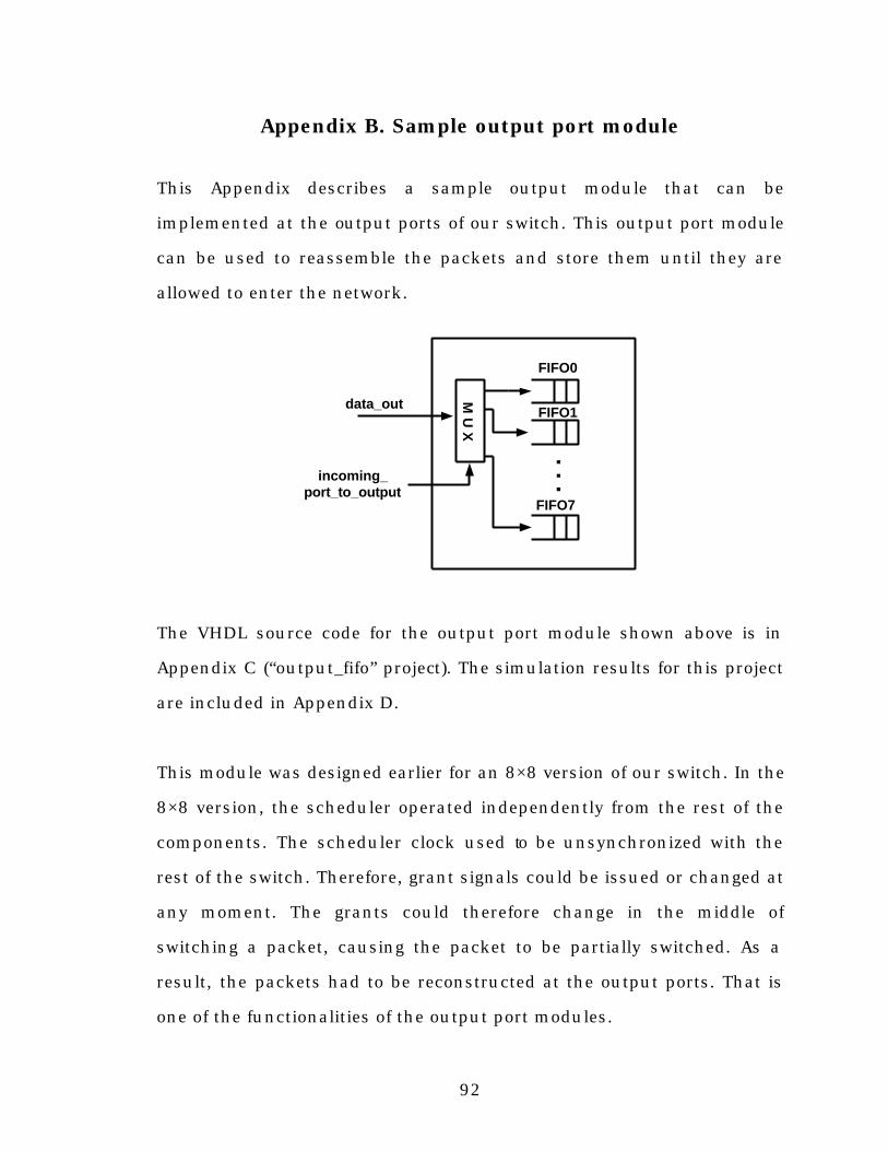
92
Appendix B. Sample output port module
This Appendix describes a sample output module that can be
implemented at the output ports of our switch. This output port module
can be used to reassemble the packets and store them until they are
allowed to enter the network.
The VHDL source code for the output port module shown above is in
Appendix C (“output_fifo” project). The simulation results for this project
are included in Appendix D.
This module was designed earlier for an 8×8 version of our switch. In the
8×8 version, the scheduler operated independently from the rest of the
components. The scheduler clock used to be unsynchronized with the
rest of the switch. Therefore, grant signals could be issued or changed at
any moment. The grants could therefore change in the middle of
switching a packet, causing the packet to be partially switched. As a
result, the packets had to be reconstructed at the output ports. That is
one of the functionalities of the output port modules.
M U
X
FIFO0
FIFO1
FIFO7
incoming_port_to_output
data_out
. . .
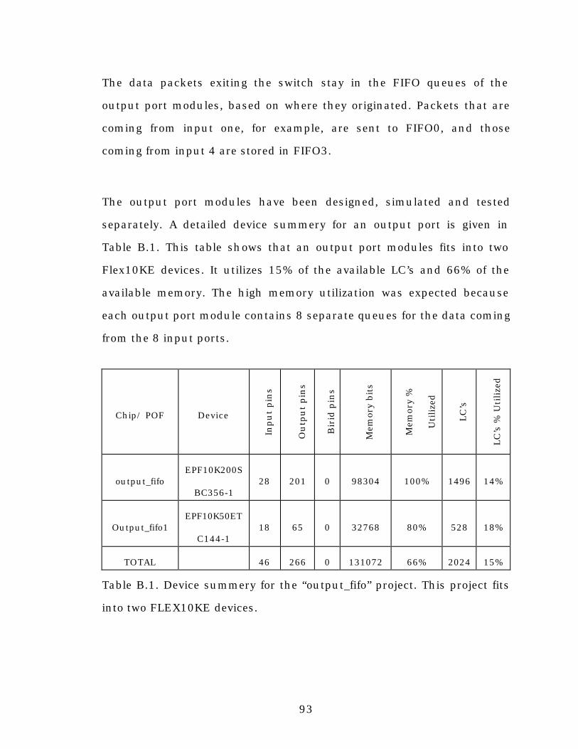
93
The data packets exiting the switch stay in the FIFO queues of the
output port modules, based on where they originated. Packets that are
coming from input one, for example, are sent to FIFO0, and those
coming from input 4 are stored in FIFO3.
The output port modules have been designed, simulated and tested
separately. A detailed device summery for an output port is given in
Table B.1. This table shows that an output port modules fits into two
Flex10KE devices. It utilizes 15% of the available LC’s and 66% of the
available memory. The high memory utilization was expected because
each output port module contains 8 separate queues for the data coming
from the 8 input ports.
Chip/ POF Device
Inpu
t pin
s
Ou
tpu
t pin
s
Bir
id p
ins
Mem
ory
bit
s
Mem
ory
%
Uti
lized
LC
’s
LC’s
% U
tilize
d
output_fifo EPF10K200S
BC356-1 28 201 0 98304 100% 1496 14%
Output_fifo1 EPF10K50ET
C144-1 18 65 0 32768 80% 528 18%
TOTAL 46 266 0 131072 66% 2024 15%
Table B.1. Device summery for the “output_fifo” project. This project fits
into two FLEX10KE devices.
94
Output port modules are the blocks where congestion control, flow
control, or policing algorithms can be implemented. An ATM switch can
only send its packets out to the network if there is consent from the
down stream node. Otherwise congestion can occur in the network, or
packets can be dropped due to buffer overflow at the destination node.
Implementation of algorithms that would handle the communication of
the network and the switch is mainly done in output port modules. For
example, a window based flow control design at the output module can
prevent bursts of data into the network. Implementation of such
algorithms is not a part of this project; therefore the de-queue process
for the output module has not been implemented. Various priority
algorithms, or any flow control scheme could be implemented for the de-
queue process.
95
Appendix C. VHDL source code for the switch and its
components
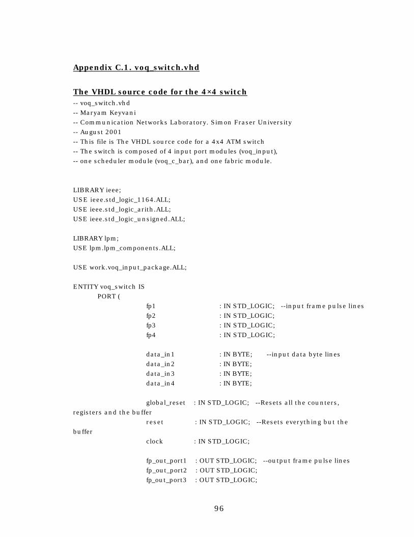
96
Appendix C.1. voq_switch.vhd
The VHDL source code for the 4×4 switch -- voq_switch.vhd -- Maryam Keyvani -- Communication Networks Laboratory. Simon Fraser University -- August 2001 -- This file is The VHDL source code for a 4x4 ATM switch -- The switch is composed of 4 input port modules (voq_input), -- one scheduler module (voq_c_bar), and one fabric module. LIBRARY ieee; USE ieee.std_logic_1164.ALL; USE ieee.std_logic_arith.ALL; USE ieee.std_logic_unsigned.ALL; LIBRARY lpm; USE lpm.lpm_components.ALL; USE work.voq_input_package.ALL; ENTITY voq_switch IS PORT ( fp1 : IN STD_LOGIC; --input frame pulse lines fp2 : IN STD_LOGIC; fp3 : IN STD_LOGIC; fp4 : IN STD_LOGIC; data_in1 : IN BYTE; --input data byte lines data_in2 : IN BYTE; data_in3 : IN BYTE; data_in4 : IN BYTE; global_reset : IN STD_LOGIC; --Resets all the counters, registers and the buffer reset : IN STD_LOGIC; --Resets everything but the buffer clock : IN STD_LOGIC; fp_out_port1 : OUT STD_LOGIC; --output frame pulse lines fp_out_port2 : OUT STD_LOGIC; fp_out_port3 : OUT STD_LOGIC;
97
fp_out_port4 : OUT STD_LOGIC; data_out_port1 : OUT BYTE; --output data_lines data_out_port2 : OUT BYTE; data_out_port3 : OUT BYTE; data_out_port4 : OUT BYTE; data_valid1 : OUT STD_LOGIC; --output data_valid lines data_valid2 : OUT STD_LOGIC; data_valid3 : OUT STD_LOGIC; data_valid4 : OUT STD_LOGIC; --Source port number incoming_port_to_output1 : OUT STD_LOGIC_VECTOR (2 DOWNTO 0); incoming_port_to_output2 : OUT STD_LOGIC_VECTOR (2 DOWNTO 0); incoming_port_to_output3 : OUT STD_LOGIC_VECTOR (2 DOWNTO 0); incoming_port_to_output4 : OUT STD_LOGIC_VECTOR (2 DOWNTO 0); --Priority vector output for simulation purpose P : OUT STD_LOGIC_VECTOR (7 DOWNTO 1); --request to scheduler and grant coming from scheduler for simulation request : OUT STD_LOGIC_VECTOR(16 DOWNTO 1); grant : OUT STD_LOGIC_VECTOR(16 DOWNTO 1) ); END voq_switch; ARCHITECTURE structure OF voq_switch IS COMPONENT voq_input GENERIC(
--Port is set to handle packets of size 53 bytes PACKET_SIZE : INTEGER:= 53;
--Counter 53 is a 6 bit counter so it can service packets upto 64 bytes long COUNTER_53_SIZE : INTEGER:= 6;
--Each data byte is 8 bits long DATA_SIZE : INTEGER:= 8;
98
--Number of words in buffer
BUFFER_SIZE : INTEGER:= 848; BUFFER_WIDTHU : INTEGER:= 10; --Recommended value is CEIL(LOG2(FIFO_SIZE))
NO_OF_BLOCKS : INTEGER:= 16; --Has to be BUFFER_SIZE/PACKET_SIZE NO_OF_QUEUES : INTEGER:= 4; --This value has to be equal to the number of output ports NO_OF_PORTS : INTEGER:= 4; VCI_VECTOR_SIZE : INTEGER:= 24; --Each VCI is 2 Bytes VCI_SIZE : INTEGER:= 16; OUTPUT_PORT_SIZE : INTEGER:= 2; --2 bits used to address an output port LUT_OUTPUT_PORT_SIZE : INTEGER := 4; -- LUT output port number size TRANSLATION_TABLE: STRING := "lut1.mif" ); PORT( data_in : IN BYTE; --STD_LOGIC_VECTOR (DATA_SIZE-1 DOWNTO 0); --Input serial data to the port clock : IN STD_LOGIC; --Input clock to the port fp : IN STD_LOGIC; --Input frame pulse to the port global_reset : IN STD_LOGIC; --Resets all the counters, registers and the FIFO reset : IN STD_LOGIC; --Resets everything but the FIFO port_grant : IN STD_LOGIC_VECTOR(3 DOWNTO 0); --The grant vector for the port port_request : OUT STD_LOGIC_VECTOR(3 DOWNTO 0); --The request vector for the port c_bar_clock : OUT STD_LOGIC; data_out_fp : OUT STD_LOGIC; --frame pulse showing the beginning of the data being shifted out data_valid : OUT STD_LOGIC; --is 1 when FIFO is dequeuing data (i.e. a grant is issued for the port) parallel_data_out : OUT STD_LOGIC_VECTOR(DATA_SIZE-1 DOWNTO 0) --the byte of data going out );
END COMPONENT;
COMPONENT voq_c_bar GENERIC (
99
NO_OF_PORTS: INTEGER := 4; -- NO_OF_GRANTS_REQ: INTEGER := 16;--Has to be NO_OF_PORTS^2 PRIO_VEC_SIZE: INTEGER := 7 --Has to be [2(NO_OF_PORTS)-1] ); PORT(
arb_req : IN std_logic_vector(NO_OF_GRANTS_REQ DOWNTO 1); clk, reset : IN std_logic; grant : OUT std_logic_vector(NO_OF_GRANTS_REQ DOWNTO 1); P : OUT std_logic_vector(7 DOWNTO 1) ); END COMPONENT; COMPONENT voq_fabric is GENERIC( SWITCH_SIZE : INTEGER:= 4; --4x4 fabric by default GRANT_SIZE : INTEGER:= 16 --16 lines used to issue grants ); PORT(
--inputs 4, 5, and 6 are made by bits from a constant matrix that is formed by input port numbers outputs 4, 5, and 6 help make the incoming_port_to_output(i)s of the switch input0 : IN DATA_VECTOR; --The 4 input data lines of type std_logic_vector(DATASIZE-1 DOWNTO 0) input1 : IN STD_LOGIC_VECTOR(SWITCH_SIZE-1 DOWNTO 0); --The 4 data_valid lines going to the fabric input2 : IN STD_LOGIC_VECTOR(SWITCH_SIZE-1 DOWNTO 0); --The LSBs of input_port_name input3 : IN STD_LOGIC_VECTOR(SWITCH_SIZE-1 DOWNTO 0); --The MSB of input_port_name input4 : IN STD_LOGIC_VECTOR(SWITCH_SIZE-1 DOWNTO 0); --The 4 input frame pulse lines cntrl : IN STD_LOGIC_VECTOR(GRANT_SIZE-1 DOWNTO 0); --The grant vector used to control the fabric output0 : OUT DATA_VECTOR; --The 4 output data lines of type std_logic_vecotr(DATASIZE-1 DOWNTO 0) output1 : OUT STD_LOGIC_VECTOR(SWITCH_SIZE-1 DOWNTO 0); --data_valid lines output2 : OUT STD_LOGIC_VECTOR(SWITCH_SIZE-1 DOWNTO 0); --The LSBs of port_name out of the fabric output3 : OUT STD_LOGIC_VECTOR(SWITCH_SIZE-1 DOWNTO 0); --The MSB of port_name out of the fabric
100
output4 : OUT STD_LOGIC_VECTOR(SWITCH_SIZE-1 DOWNTO 0) --the 4 output frame pulses for the 8 output ports ); END COMPONENT; SIGNAL arb_req_signal: STD_LOGIC_VECTOR (16 DOWNTO 1); --grant_signal connects the grant output of the c_bar scheduler, which is a 64 bit vector, to the cntrl input of the fabric. SIGNAL grant_signal : STD_LOGIC_VECTOR (16 DOWNTO 1); --the grant signal coming from the scheduler SIGNAL input_data : DATA_VECTOR; --Connects data_out coming out of port to fabric input --output_data connects the fabric data output (output(i)) to output data line of the switch ((data_out_port(i)) SIGNAL output_data : DATA_VECTOR; --input_fp connects the outgoing data's fp comming from the input port (data_out_fp) to the fabric input SIGNAL input_fp : STD_LOGIC_VECTOR (4 DOWNTO 1); --output_fp connects the fabric frame pulse output (output2) to frame pulse output of the switch ((fp_out_port(i)) SIGNAL output_fp : STD_LOGIC_VECTOR (4 DOWNTO 1); --Reset signal for crossbar scheduler SIGNAL resetb :STD_LOGIC; SIGNAL input_port_name_bits1 : STD_LOGIC_VECTOR(3 DOWNTO 0); --Will be hard coded to "1100" SIGNAL input_port_name_bits0 : STD_LOGIC_VECTOR(3 DOWNTO 0);--Will be hard coded to "1010" SIGNAL source_to_output1 : STD_LOGIC_VECTOR(1 DOWNTO 0); --used to build the source port number (incoming_port_to_output1) SIGNAL source_to_output2 : STD_LOGIC_VECTOR(1 DOWNTO 0); --used to build the source port number (incoming_port_to_output2)
101
SIGNAL source_to_output3 : STD_LOGIC_VECTOR(1 DOWNTO 0); --used to build the source port number (incoming_port_to_output3) SIGNAL source_to_output4 : STD_LOGIC_VECTOR(1 DOWNTO 0); --used to build the source port number (incoming_port_to_output4) --Signals needed to carry control info to the output ports --data_valid_signal connects output3 of the fabric to data_valid(i), which is the output of the switch SIGNAL data_valid_signal : STD_LOGIC_VECTOR (4 DOWNTO 1); SIGNAL data_valid_to_fabric : STD_LOGIC_VECTOR (4 DOWNTO 1);--Connects data_valid comming from each port to input3 going to the fabric. SIGNAL port_name_bit0 : STD_LOGIC_VECTOR (4 DOWNTO 1);--Connected to the output4 of the fabric SIGNAL port_name_bit1 : STD_LOGIC_VECTOR (4 DOWNTO 1);--Connected to the output5 of the fabric SIGNAL packet_clock : STD_LOGIC; BEGIN --Output data lines of the switch are constructed here --output_data is a vector that connects outgoing data from the fabric to outgoing data of the switch data_out_port1 <= output_data(0); data_out_port2 <= output_data(1); data_out_port3 <= output_data(2); data_out_port4 <= output_data(3); --Outgoing frame pulse lines of the switch are constructed here --output_fp is a vector that connects the outgoing frame pulse from the fabric to outgoing fp of the switch fp_out_port1 <= output_fp(1); fp_out_port2 <= output_fp(2); fp_out_port3 <= output_fp(3); fp_out_port4 <= output_fp(4); data_valid1 <= data_valid_signal(1); data_valid2 <= data_valid_signal(2); data_valid3 <= data_valid_signal(3);
102
data_valid4 <= data_valid_signal(4); source_to_output1 <= port_name_bit1(1) & port_name_bit0(1); source_to_output2 <= port_name_bit1(2) & port_name_bit0(2); source_to_output3 <= port_name_bit1(3) & port_name_bit0(3); source_to_output4 <= port_name_bit1(4) & port_name_bit0(4); incoming_port_to_output1 <= source_to_output1 + "001"; incoming_port_to_output2 <= source_to_output2 + "001"; incoming_port_to_output3 <= source_to_output3 + "001"; incoming_port_to_output4 <= source_to_output4 + "001"; --These vectors are connected to the fabric and according to the configuration of the fabric and the grants that are given, the number of the input port that was granted a request comes to the output of the fabric input_port_name_bits1 <= "1100"; input_port_name_bits0 <= "1010"; request <= arb_ req_signal; grant <= grant_signal; resetb <= NOT global_reset; --**************** Component instantiation ***************************** --Instances of ports 1 to 4 port1: voq_input GENERIC MAP ( TRANSLATION_TABLE => "lut1.mif" ) PORT MAP (
data_in => data_in1, clock => clock, fp => fp1, global_reset => global_reset,
reset => reset, queue3_out => queue3_out1, free_space_out => free_space_out1,
ready_flag_out => ready_flag_out1, port_grant => grant_signal (4 downto 1), parallel_data_out => input_data(0), port_request => arb_req_signal (4 downto 1),
103
c_bar_clock => packet_clock, data_out_fp => input_fp(1),
data_valid => data_valid_to_fabric(1) ); port2: voq_input GENERIC MAP ( TRANSLATION_TABLE => "lut2.mif" ) PORT MAP ( data_in => data_in2, clock => clock, fp => fp2, global_reset => global_reset, reset => reset, port_grant => grant_signal (8 downto 5), parallel_data_out => input_data(1), port_request => arb_req_signal (8 downto 5), data_out_fp => input_fp(2), data_valid => data_valid_ to_fabric(2) ); port3: voq_input GENERIC MAP ( TRANSLATION_TABLE => "lut3.mif" ) PORT MAP ( data_in => data_in3, clock => clock, fp => fp3, global_reset => global_reset, reset => reset, port_grant => grant_signal (12 downto 9), parallel_data_out => input_data(2), port_request => arb_req_signal (12 downto 9), data_out_fp => input_fp(3), data_valid => data_valid_to_fabric(3) );
104
port4: voq_input GENERIC MAP ( TRANSLATION_TABLE => "lut4.mif" ) PORT MAP ( data_in => data_in4, clock => clock, fp => fp4, global_reset => global_reset, reset => reset, port_grant => grant_signal (16 downto 13), parallel_data_out => input_data(3), port_request => arb_req_signal (16 downto 13), data_out_fp => input_fp(4), data_valid => data_valid_to_fabric(4) ); switch_c_bar: voq_c_bar PORT MAP ( arb_req => arb_req_signal, clk => packet_clock, reset => resetb, grant => grant_signal, P => P ); --Instance of the fabric data_fabric: voq_fabric PORT MAP ( input0 => input_data, input1 => input_fp, input2 => data_valid_to_fabric, input3 => input_port_name_bits0, input4 => input_port_name_bits1, cntrl => grant_signal, output0 => output_data, output1 => output_fp, output2 => data_valid_signal,

105
output3 => port_name_bit0, output4 => port_name_bit1 ); END structure;
106
Appendix C.2. voq_input.vhd
VHDL source code for the input port module of the switch -- voq_input.vhd -- Maryam Keyvani -- Commuication Networks Laboratory, Simon Fraser University -- August 2001 -- This file contains VHDL description of the input port modules used in the voq_switch project. -- The input port module, receives the incoming packets, stores them in buffer, looks up packet header, -- determines destination port number, updates packet header, sends a request for the destination port -- to the scheduler, and sends the packet out once a grant is received. LIBRARY ieee; USE ieee.std_logic_1164.ALL; USE ieee.std_logic_arith.ALL; USE ieee.std_logic_unsigned.ALL; LIBRARY lpm; USE lpm.lpm_components.ALL; USE work.voq_input_package.ALL; ENTITY voq_input IS GENERIC( PACKET_SIZE : INTEGER:= 53; --Port is set to handle packets of size 53 bytes COUNTER_53_SIZE : INTEGER:= 6; --Counter_53 is a 6 bit counter. DATA_SIZE : INTEGER:= 8; --Each data byte is 8 bits long BUFFER_SIZE : INTEGER:= 848; --Number of words in buffer BUFFER_WIDTHU : INTEGER:= 10; --Recommeneded value is CEIL(LOG2(BUFFER_SIZE)) NO_OF_BLOCKS : INTEGER:= 16; --Has to be BUFFER_SIZE/PACKET_SIZE NO_OF_QUEUES : INTEGER:= 4; --This value has to be equal to the number of output ports NO_OF_PORTS : INTEGER:= 4; VCI_VECTOR_SIZE : INTEGER:= 24; VCI_SIZE : INTEGER:= 16; --Each VCI is 2 Bytes. OUTPUT_PORT_SIZE : INTEGER:= 2; --2 bits used to address an output port LUT_OUTPUT_PORT_SIZE: INTEGER:= 4; TRANSLATION_TABLE : STRING := "lut1.mif" );
107
PORT( --Test Signals for simulation purposes state :OUT INTEGER RANGE 0 TO 7; cntrl_state :OUT INTEGER RANGE 0 TO 7; DQ_state : OUT INTEGER RANGE 0 TO 15; count53_out : OUT STD_LOGIC_VECTOR(COUNTER_53_SIZE-1 DOWNTO 0); c53sset_out : OUT STD_LOGIC; input_vci_out : OUT STD_LOGIC_VECTOR (VCI_SIZE-1 DOWNTO 0); --Signal that goes to LUT to be looked up output_vci_out : OUT STD_LOGIC_VECTOR (VCI_SIZE-1 DOWNTO 0); --The updated VCI output_port_no_out : OUT STD_LOGIC_VECTOR (LUT_OUTPUT_PORT_SIZE-1 DOWNTO 0); --The destination output port out_vci_ready_out : OUT STD_LOGIC; -- Indicates whether output VCI and port no. are ready for pickup destination_port_no_out: OUT STD_LOGIC_VECTOR(OUTPUT_PORT_SIZE-1 DOWNTO 0); vci_in_vector_out : OUT VCI_VECTOR_TYPE; VCI_reg_en_out : OUT STD_LOGIC; -- Buffer signals buffer_output : OUT STD_LOGIC_VECTOR(DATA_SIZE-1 DOWNTO 0); wr_address_signal_out : OUT STD_LOGIC_VECTOR(BUFFER_WIDTHU-1 DOWNTO 0); rd_address_signal_out : OUT STD_LOGIC_VECTOR(BUFFER_WIDTHU-1 DOWNTO 0); wr_en_signal_out : OUT STD_LOGIC; rd_en_signal_out : OUT STD_LOGIC; dq_count53_out : OUT STD_LOGIC_VECTOR (COUNTER_53_SIZE-1 DOWNTO 0); dq_count53_temp_out : OUT STD_LOGIC_VECTOR (COUNTER_53_SIZE-1 DOWNTO 0); --linked lists queue0_head_out : OUT POINTER; queue0_tail_out : OUT POINTER; queue0_empty_out : OUT STD_LOGIC; queue0_out : OUT QUEUE_DESCRIPTOR; queue1_out : OUT QUEUE_DESCRIPTOR; queue2_out : OUT QUEUE_DESCRIPTOR; queue3_out : OUT QUEUE_DESCRIPTOR;
108
free_space_out : OUT QUEUE_DESCRIPTOR; free_space_head_out : OUT POINTER; free_space_tail_out : OUT POINTER; free_space_empty_out : OUT STD_LOGIC; next_register_out : OUT NEXT_REGISTER_TYPE; ready_flag_out : OUT STD_LOGIC_VECTOR (NO_OF_BLOCKS-1 DOWNTO 0); read_pointer_out : OUT INTEGER RANGE 0 to 15; --Points to the block that has to be read read_queue_out : OUT INTEGER RANGE 0 to 3; --Is the queue number that is being read from queue_no_out : OUT INTEGER RANGE 0 to 3; --Is the queue number that is being written to --Actual entity ports data_in : IN STD_LOGIC_VECTOR (DATA_SIZE-1 DOWNTO 0); --Prallel data byte input clock : IN STD_LOGIC; --Input clock to the port c_bar_clock : OUT STD_LOGIC; --Used for loading request, and issuing grants fp : IN STD_LOGIC; --Input frame pulse to the port global_reset : IN STD_LOGIC; --Resets all the counters, registers and the BUFFER reset : IN STD_LOGIC; --Resets everything but the BUFFER port_grant : IN STD_LOGIC_VECTOR(3 DOWNTO 0); --The grant vector for the port port_request : OUT STD_LOGIC_VECTOR(3 DOWNTO 0); --The request vector for the port data_out_fp : OUT STD_LOGIC; --Frame pulse showing the beginning of the outgoing packet data_valid : OUT STD_LOGIC; --is 1 when buffer is dequeuing data parallel_data_out : OUT STD_LOGIC_VECTOR(DATA_SIZE-1 DOWNTO 0) --Prallel data byte output ); END voq_input; ARCHITECTURE behav OF voq_input IS --Component Declaration COMPONENT LUT GENERIC (VCI_SIZE: INTEGER := 16; PORT_SIZE: INTEGER := 4;
109
ROM_WIDTH : INTEGER := 36; --width of the look up table ROM_WIDTHAD : INTEGER := 3; --Address width of LUT=log2(number of rows in table) TRANSLATION_TABLE: STRING ); PORT ( input_vci : IN STD_LOGIC_VECTOR (VCI_SIZE-1 downto 0); output_port_no: OUT STD_LOGIC_VECTOR (PORT_SIZE-1 downto 0 ); output_vci : OUT STD_LOGIC_VECTOR (VCI_SIZE-1 downto 0); clock : IN STD_LOGIC; renable : OUT STD_LOGIC ); END COMPONENT; FUNCTION ENCODE (s: STD_LOGIC_VECTOR (3 DOWNTO 0)) --Used to translate grant signal to a queue number RETURN INTEGER IS VARIABLE INT: INTEGER RANGE 0 to 3; BEGIN CASE s IS WHEN "1000" => INT := 3; WHEN "0100" => INT := 2; WHEN "0010" => INT := 1; WHEN "0001" => INT := 0; WHEN OTHERS => NULL; END CASE; RETURN INT; END FUNCTION; ------------------------------------------------------------------------------------------------------ --************************************* SIGNALS ************************************************* ---------------------------------------------------------------------------------------------------- -- BUFFER signals SIGNAL rd_en_signal : STD_LOGIC; SIGNAL wr_en_signal : STD_LOGIC; SIGNAL RAM_out : STD_LOGIC_VECTOR(DATA_SIZE-1 DOWNTO 0); SIGNAL rd_address_signal : STD_LOGIC_VECTOR(BUFFER_WIDTHU-1 DOWNTO 0); SIGNAL wr_address_signal : STD_LOGIC_VECTOR(BUFFER_WIDTHU-1 DOWNTO 0); -- VCI registers and signals SIGNAL VCI_reg_en : STD_LOGIC; --Loads VCI registers with VCI bytes SIGNAL VCI_reg0_out : BYTE; --Output of the first VCI register SIGNAL VCI_reg1_out : BYTE; --Output of the second VCI register SIGNAL VCI_reg2_out : BYTE; --Output of the third VCI register
110
SIGNAL vci_in_vector : VCI_VECTOR_TYPE; --Where the incoming vci vector is stored SIGNAL vci_out_vector : VCI_VECTOR_ARRAY_TYPE; --Where the updated vci is stored. One exists for each block. SIGNAL input_vci : STD_LOGIC_VECTOR (VCI_SIZE-1 DOWNTO 0); --Connected to input of LUT --registers and flags SIGNAL next_register : NEXT_REGISTER_TYPE; --The next block in the linked list SIGNAL ready_flag : STD_LOGIC_VECTOR (NO_OF_BLOCKS-1 DOWNTO 0); --Shows a complete packet has been written --Queue linked list pointers SIGNAL temp : POINTER; --Latches the value of free_space.head SIGNAL free_space : QUEUE_DESCRIPTOR; --The free space linked list. SIGNAL queue : QUEUE_TYPE; --An array of all 4 linked lists(queues) SIGNAL read_pointer : INTEGER RANGE 0 to 15; --Points to the block that has to be read SIGNAL read_queue : INTEGER RANGE 0 to 3; --Is the queue number that is being read from SIGNAL queue_no : INTEGER RANGE 0 to 3; --Is the queue number that is being written to SIGNAL HIGH : STD_LOGIC; SIGNAL LOW : STD_LOGIC; --Counter_53 Signals SIGNAL count53 : STD_LOGIC_VECTOR (COUNTER_53_SIZE-1 DOWNTO 0); --6 Bit output of counter 53 SIGNAL c53sset : STD_LOGIC; --Synchronous clear for counter_53 --Dequeue counter 53 Signals SIGNAL dq_c53aclr : STD_LOGIC; --Asynchronous clear for dq_counter53 SIGNAL dq_count53 : STD_LOGIC_VECTOR (COUNTER_53_SIZE-1 DOWNTO 0); --6 Bit output of dq counter 53 SIGNAL dq_c53aset : STD_LOGIC; --Is always set to LOW SIGNAL data_valid_signal : STD_LOGIC; --Shows when the data on the output line is valid SIGNAL dq_count53_temp : STD_LOGIC_VECTOR (COUNTER_53_SIZE-1 DOWNTO 0);--Holds dp_count53 value for 2 extra clocks SIGNAL dq_count53_temp_next : STD_LOGIC_VECTOR (COUNTER_53_SIZE-1 DOWNTO 0); SIGNAL count59 : STD_LOGIC_VECTOR (COUNTER_53_SIZE-1 DOWNTO 0);--Used to construct of c_bar_clock --LUT Signals
111
SIGNAL output_port_no : STD_LOGIC_VECTOR (LUT_OUTPUT_PORT_SIZE-1 DOWNTO 0); --The destination output port number SIGNAL output_vci : STD_LOGIC_VECTOR (VCI_SIZE-1 DOWNTO 0); --The VCI to be placed in the outgoing packet SIGNAL out_vci_ready : STD_LOGIC; --When 1, output VCI and port no. are ready for pickup SIGNAL lut_clock : STD_LOGIC; --The clock that will be connected to LUT through lut_run clock. SIGNAL lut_clock_signal : STD_LOGIC; --State Machines SIGNAL current_state : INTEGER RANGE 0 TO 7; SIGNAL next_state : INTEGER RANGE 0 TO 7; SIGNAL cntrl_current_state : INTEGER RANGE 0 TO 7; SIGNAL cntrl_next_state : INTEGER RANGE 0 TO 7; SIGNAL DQ_current_state : INTEGER RANGE 0 TO 15; SIGNAL DQ_next_state : INTEGER RANGE 0 TO 15; --Processor Specific Signals SIGNAL destination_port_no : STD_LOGIC_VECTOR(OUTPUT_PORT_SIZE -1 DOWNTO 0); --The destination port number. SIGNAL port_req : STD_LOGIC_VECTOR(NO_OF_PORTS-1 DOWNTO 0); --The request vector to be sent out SIGNAL parallel_data : STD_LOGIC_VECTOR(DATA_SIZE-1 DOWNTO 0); --Data bytes going out of voq_input SIGNAL data_out_fp_signal : STD_LOGIC; --Frame pulse output SIGNAL request_clock : STD_LOGIC; --Same as c_bar_clock BEGIN -- Output signal assignments for test and simulation purpose state <= current_state; count53_out <= count53; c53sset_out <= c53sset; output_port_no_out <= output_port_no; output_vci_out <= output_vci; out_vci_ready_out <= out_vci_ready; input_vci_out <= input_vci; destination_port_no_out <= destination_port_no; vci_in_vector_out <= vci_in_vector; VCI_reg_en_out <= VCI_reg_en; dq_count53_out <= dq_count53; dq_count53_temp_out <= dq_count53_temp; parallel_data_out <= parallel_data; data_out_fp <= data_out_fp_signal;
112
data_valid <= data_valid_signal; cntrl_state <= cntrl_current_state; DQ_state <= DQ_current_state; --linked lists queue0_head_out <= queue(0).head; queue0_tail_out <= queue(0).tail; queue0_empty_out <= queue(0).empty; queue0_out <= queue(0); queue1_out <= queue(1); queue2_out <= queue(2); queue3_out <= queue(3); free_space_out <= free_space; free_space_head_out <= free_space.head; free_space_tail_out <= free_space.tail; free_space_empty_out <= free_space.empty; next_register_out <= next_register; ready_flag_out <= ready_flag; read_queue_out <= read_queue; queue_no_out <= queue_no; read_pointer_out <= read_pointer; --Buffer signals and ports wr_address_signal_out <= wr_address_signal; rd_address_signal_out <= rd_address_signal; wr_en_signal_out <= wr_en_signal; rd_en_signal_out <= rd_en_signal; buffer_output <= RAM_out; c_bar_clock <= request_clock; Write_Seq_SM : PROCESS (clock) BEGIN --Process IF (clock='0' AND clock'event) THEN --At the falling edge of clock next state is calculated IF ((global_reset = '0') AND (reset = '0')) THEN CASE current_state IS WHEN 0 =>
wr_en_signal <= '0'; VCI_reg_en <= '0'; --If new packet coming and buffer has free space IF ( fp = '1' ) AND (free_space.empty = '0') THEN
next_state <= 1; temp <= free_space.head; --Keep first byte of new packet in a temp
113
c53sset <= '0';--start counting if there is a frame pulse ELSE c53sset <= '1'; END IF; --This is the RAM address where the data byte is written WHEN 1 =>
wr_address_signal <= count53 + ((free_space.head)* "110101"); wr_en_signal <= '1'; --Write the one byte of data that is
coming in IF (count53 /= "110100") THEN --Continue reading the remaining bits of packet next_state <= 1; ELSE --If the whole packet has been received
next_state <= 0; c53sset <= '1'; END IF;
-- Send VCI bytes (bytes 2,3 and 4 of the header) to the VCI registers IF ((count53 = "00001") OR (count53 = "00010") OR (count53 = "000011")) THEN
VCI_reg_en <= '1';
ELSE VCI_reg_en <= '0'; END IF; WHEN OTHERS => NULL; END CASE; ELSE --In case of reset or if buffer is full, drop the incoming packet
IF ( (global_reset = '1') OR (reset = '1') OR (free_space.empty = '1')) THEN
next_state <= 0; wr_en_signal <= '0'; c53sset <= '1'; END IF; END IF; END IF; END PROCESS; PROCESS (clock) --State update process BEGIN
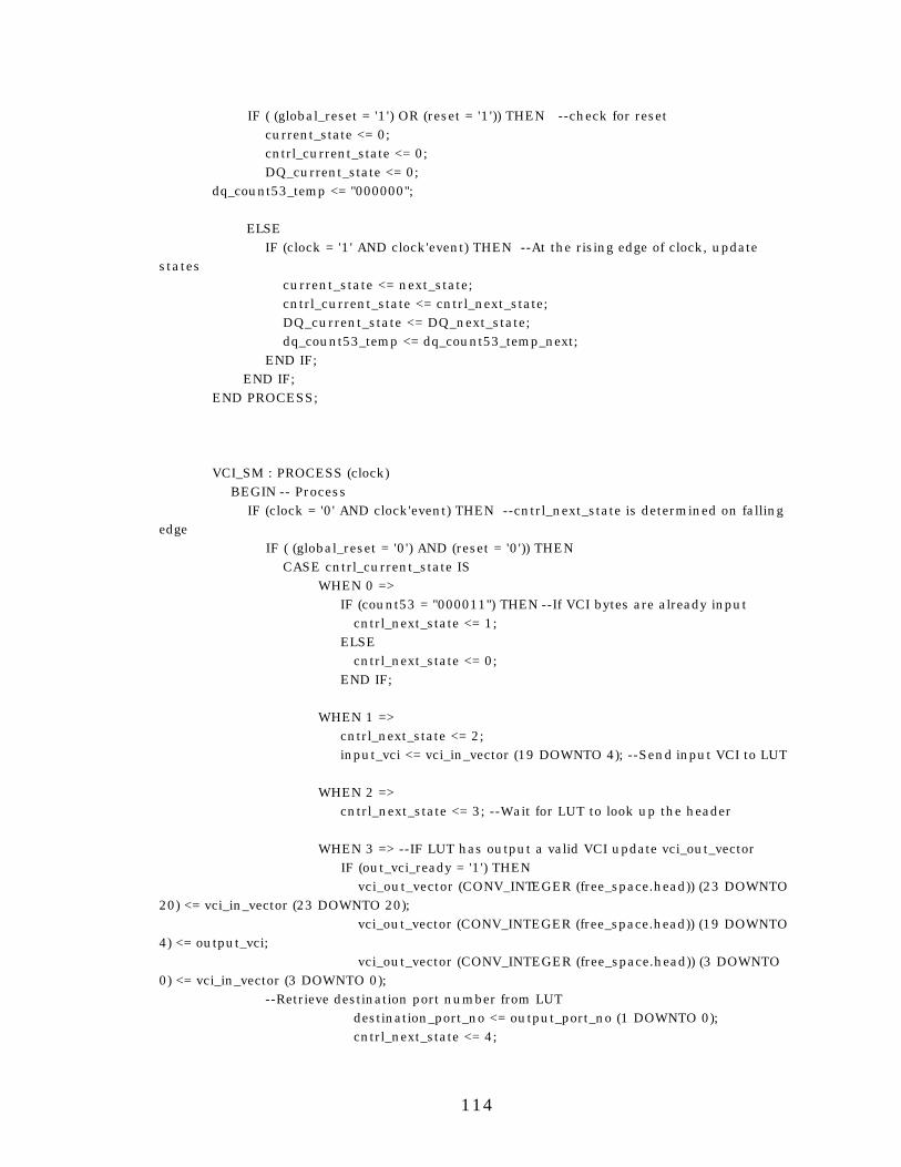
114
IF ( (global_reset = '1') OR (reset = '1')) THEN --check for reset current_state <= 0; cntrl_current_state <= 0; DQ_current_state <= 0; dq_count53_temp <= "000000"; ELSE IF (clock = '1' AND clock'event) THEN --At the rising edge of clock, update states current_state <= next_state; cntrl_current_state <= cntrl_next_state; DQ_current_state <= DQ_next_state; dq_count53_temp <= dq_count53_temp_next; END IF; END IF; END PROCESS; VCI_SM : PROCESS (clock) BEGIN -- Process IF (clock = '0' AND clock'event) THEN --cntrl_next_state is determined on falling edge IF ( (global_reset = '0') AND (reset = '0')) THEN CASE cntrl_current_state IS WHEN 0 => IF (count53 = "000011") THEN --If VCI bytes are already input cntrl_next_state <= 1; ELSE cntrl_next_state <= 0; END IF; WHEN 1 => cntrl_next_state <= 2; input_vci <= vci_in_vector (19 DOWNTO 4); --Send input VCI to LUT WHEN 2 => cntrl_next_state <= 3; --Wait for LUT to look up the header WHEN 3 => --IF LUT has output a valid VCI update vci_out_vector IF (out_vci_ready = '1') THEN vci_out_vector (CONV_INTEGER (free_space.head)) (23 DOWNTO 20) <= vci_in_vector (23 DOWNTO 20); vci_out_vector (CONV_INTEGER (free_space.head)) (19 DOWNTO 4) <= output_vci; vci_out_vector (CONV_INTEGER (free_space.head)) (3 DOWNTO 0) <= vci_in_vector (3 DOWNTO 0); --Retrieve destination port number from LUT destination_port_no <= output_port_no (1 DOWNTO 0); cntrl_next_state <= 4;
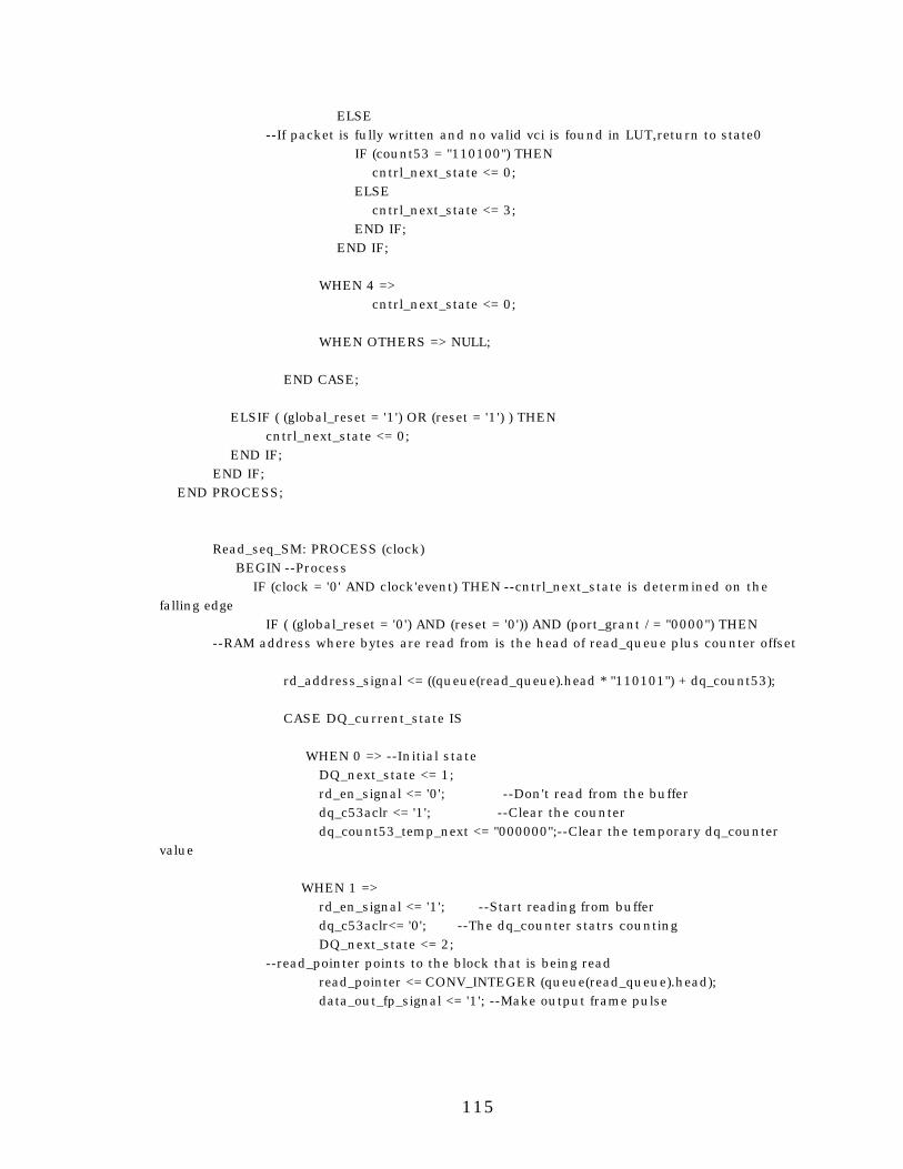
115
ELSE --If packet is fully written and no valid vci is found in LUT,return to state0 IF (count53 = "110100") THEN cntrl_next_state <= 0; ELSE cntrl_next_state <= 3; END IF; END IF; WHEN 4 => cntrl_next_state <= 0; WHEN OTHERS => NULL; END CASE; ELSIF ( (global_reset = '1') OR (reset = '1') ) THEN cntrl_next_state <= 0; END IF;
END IF; END PROCESS; Read_seq_SM: PROCESS (clock) BEGIN --Process IF (clock = '0' AND clock'event) THEN --cntrl_next_state is determined on the falling edge IF ( (global_reset = '0') AND (reset = '0')) AND (port_grant /= "0000") THEN --RAM address where bytes are read from is the head of read_queue plus counter offset rd_address_signal <= ((queue(read_queue).head * "110101") + dq_count53); CASE DQ_current_state IS WHEN 0 => --Initial state DQ_next_state <= 1; rd_en_signal <= '0'; --Don't read from the buffer dq_c53aclr <= '1'; --Clear the counter dq_count53_temp_next <= "000000";--Clear the temporary dq_counter value WHEN 1 => rd_en_signal <= '1'; --Start reading from buffer dq_c53aclr<= '0'; --The dq_counter statrs counting DQ_next_state <= 2; --read_pointer points to the block that is being read read_pointer <= CONV_INTEGER (queue(read_queue).head); data_out_fp_signal <= '1'; --Make output frame pulse
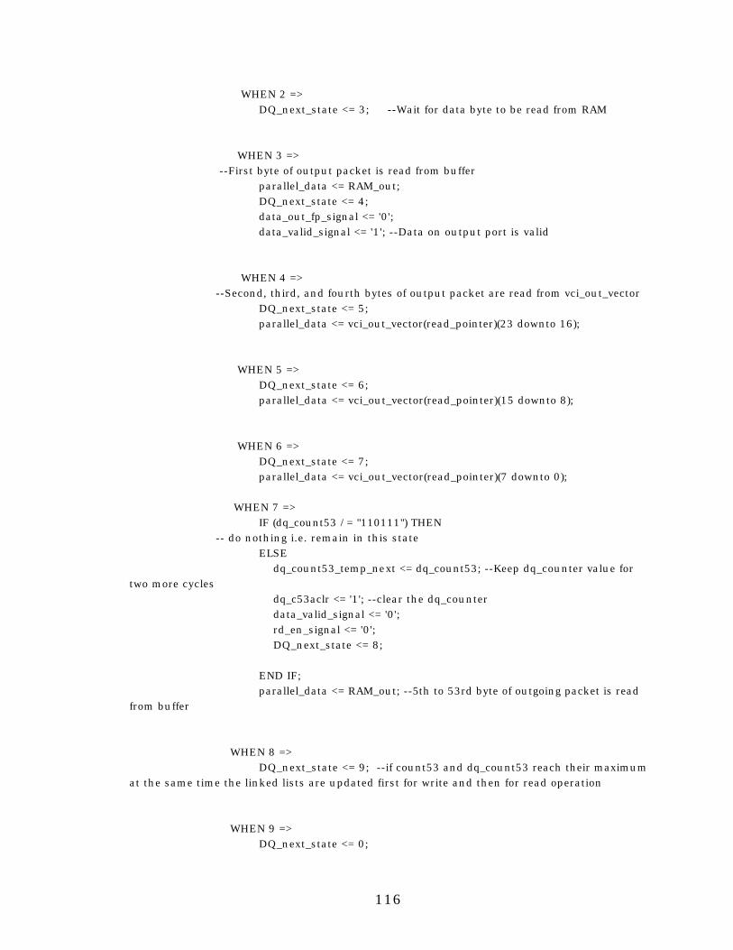
116
WHEN 2 => DQ_next_state <= 3; --Wait for data byte to be read from RAM WHEN 3 => --First byte of output packet is read from buffer parallel_data <= RAM_out; DQ_next_state <= 4; data_out_fp_signal <= '0'; data_valid_signal <= '1'; --Data on output port is valid WHEN 4 => --Second, third, and fourth bytes of output packet are read from vci_out_vector DQ_next_state <= 5; parallel_data <= vci_out_vector(read_pointer)(23 downto 16); WHEN 5 => DQ_next_state <= 6; parallel_data <= vci_out_vector(read_pointer)(15 downto 8); WHEN 6 => DQ_next_state <= 7; parallel_data <= vci_out_vector(read_pointer)(7 downto 0); WHEN 7 => IF (dq_count53 /= "110111") THEN -- do nothing i.e. remain in this state ELSE dq_count53_temp_next <= dq_count53; --Keep dq_counter value for two more cycles dq_c53aclr <= '1'; --clear the dq_counter data_valid_signal <= '0'; rd_en_signal <= '0'; DQ_next_state <= 8; END IF; parallel_data <= RAM_out; --5th to 53rd byte of outgoing packet is read from buffer WHEN 8 => DQ_next_state <= 9; --if count53 and dq_count53 reach their maximum at the same time the linked lists are updated first for write and then for read operation WHEN 9 => DQ_next_state <= 0;
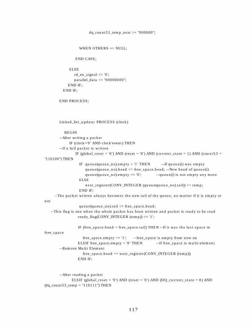
117
dq_count53_temp_next <= "000000"; WHEN OTHERS => NULL; END CASE; ELSE rd_en_signal <= '0'; parallel_data <= "00000000"; END IF; END IF; END PROCESS; Linked_list_update: PROCESS (clock) BEGIN --After writing a packet IF (clock='0' AND clock'event) THEN --If a full packet is written IF (global_reset = '0') AND (reset = '0') AND (current_state = 1) AND (count53 = "110100") THEN IF queue(queue_no).empty = '1' THEN --If queue(i) was empty queue(queue_no).head <= free_space.head; --New head of queue(i) queue(queue_no).empty <= '0'; --queue(i) is not empty any more ELSE next_register(CONV_INTEGER (queue(queue_no).tail)) <= temp; END IF; --The packet written always becomes the new tail of the queue, no matter if it is empty or not queue(queue_no).tail <= free_space.head; --This flag is one when the whole packet has been written and packet is ready to be read ready_flag(CONV_INTEGER (temp)) <= '1'; IF (free_space.head = free_space.tail) THEN --If it was the last space in free_space free_space.empty <= '1'; --free_space is empty from now on ELSIF free_space.empty = '0' THEN --If free_space is multi-element --Remove Multi Element free_space.head <= next_register(CONV_INTEGER (temp)); END IF;
--After reading a packet ELSIF (global_reset = '0') AND (reset = '0') AND (DQ_current_state = 8) AND (dq_count53_temp = "110111") THEN
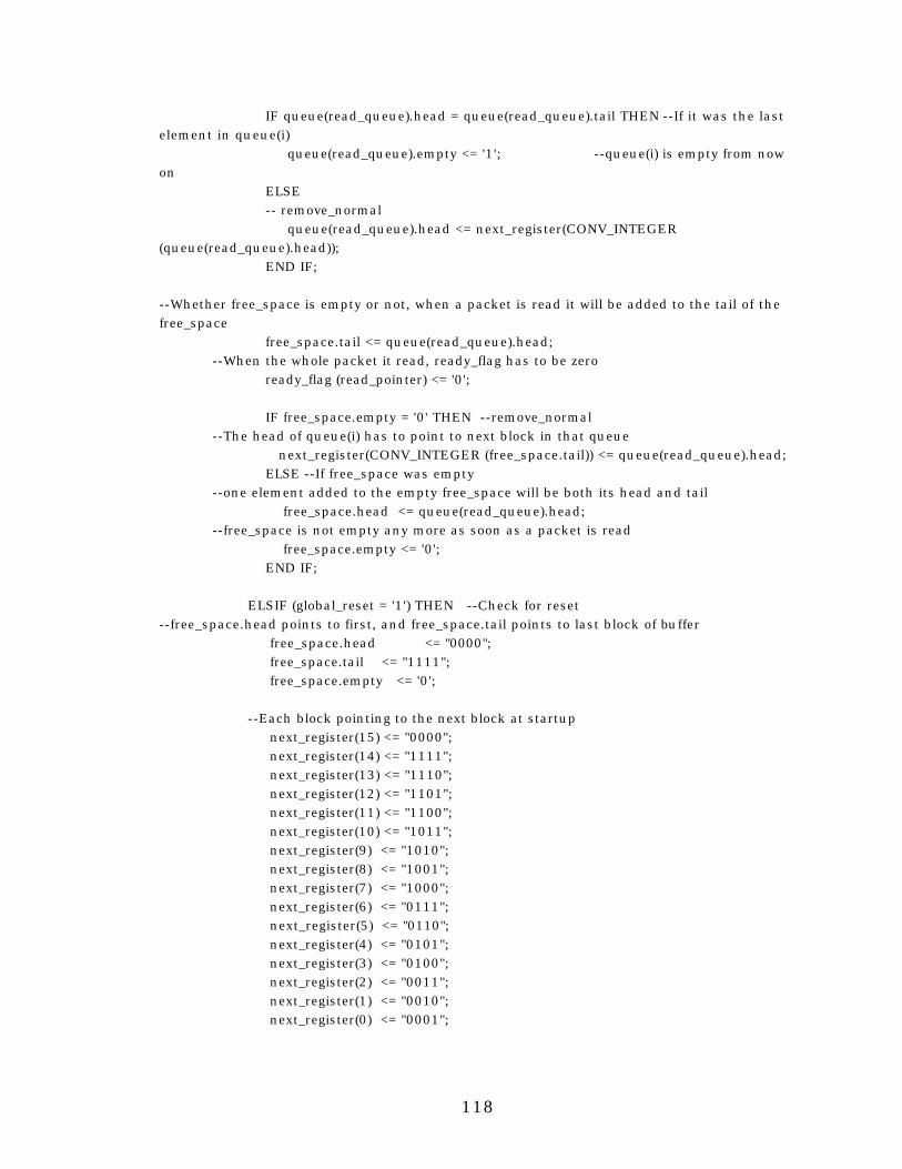
118
IF queue(read_queue).head = queue(read_queue).tail THEN --If it was the last element in queue(i) queue(read_queue).empty <= '1'; --queue(i) is empty from now on ELSE -- remove_normal queue(read_queue).head <= next_register(CONV_INTEGER (queue(read_queue).head)); END IF; --Whether free_space is empty or not, when a packet is read it will be added to the tail of the free_space free_space.tail <= queue(read_queue).head; --When the whole packet it read, ready_flag has to be zero ready_flag (read_pointer) <= '0'; IF free_space.empty = '0' THEN --remove_normal --The head of queue(i) has to point to next block in that queue next_register(CONV_INTEGER (free_space.tail)) <= queue(read_queue).head; ELSE --If free_space was empty --one element added to the empty free_space will be both its head and tail free_space.head <= queue(read_queue).head; --free_space is not empty any more as soon as a packet is read free_space.empty <= '0'; END IF; ELSIF (global_reset = '1') THEN --Check for reset --free_space.head points to first, and free_space.tail points to last block of buffer free_space.head <= "0000"; free_space.tail <= "1111"; free_space.empty <= '0'; --Each block pointing to the next block at startup next_register(15) <= "0000"; next_register(14) <= "1111"; next_register(13) <= "1110"; next_register(12) <= "1101"; next_register(11) <= "1100"; next_register(10) <= "1011"; next_register(9) <= "1010"; next_register(8) <= "1001"; next_register(7) <= "1000"; next_register(6) <= "0111"; next_register(5) <= "0110"; next_register(4) <= "0101"; next_register(3) <= "0100"; next_register(2) <= "0011"; next_register(1) <= "0010"; next_register(0) <= "0001";
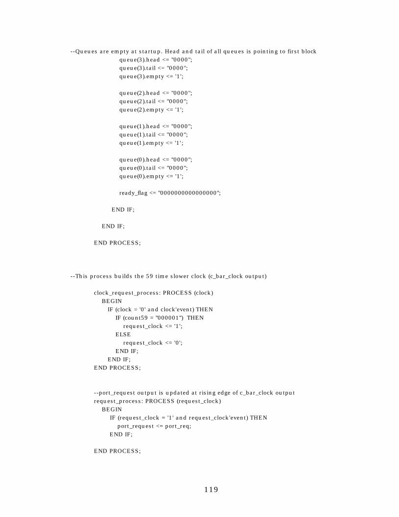
119
--Queues are empty at startup. Head and tail of all queues is pointing to first block queue(3).head <= "0000"; queue(3).tail <= "0000"; queue(3).empty <= '1'; queue(2).head <= "0000"; queue(2).tail <= "0000"; queue(2).empty <= '1'; queue(1).head <= "0000"; queue(1).tail <= "0000"; queue(1).empty <= '1';
queue(0).head <= "0000"; queue(0).tail <= "0000"; queue(0).empty <= '1'; ready_flag <= "0000000000000000"; END IF; END IF; END PROCESS; --This process builds the 59 time slower clock (c_bar_clock output) clock_request_process: PROCESS (clock) BEGIN IF (clock = '0' and clock'event) THEN IF (count59 = "000001") THEN request_clock <= '1'; ELSE request_clock <= '0'; END IF; END IF; END PROCESS;
--port_request output is updated at rising edge of c_bar_clock output request_process: PROCESS (request_clock)
BEGIN IF (request_clock = '1' and request_clock'event) THEN port_request <= port_req; END IF; END PROCESS;
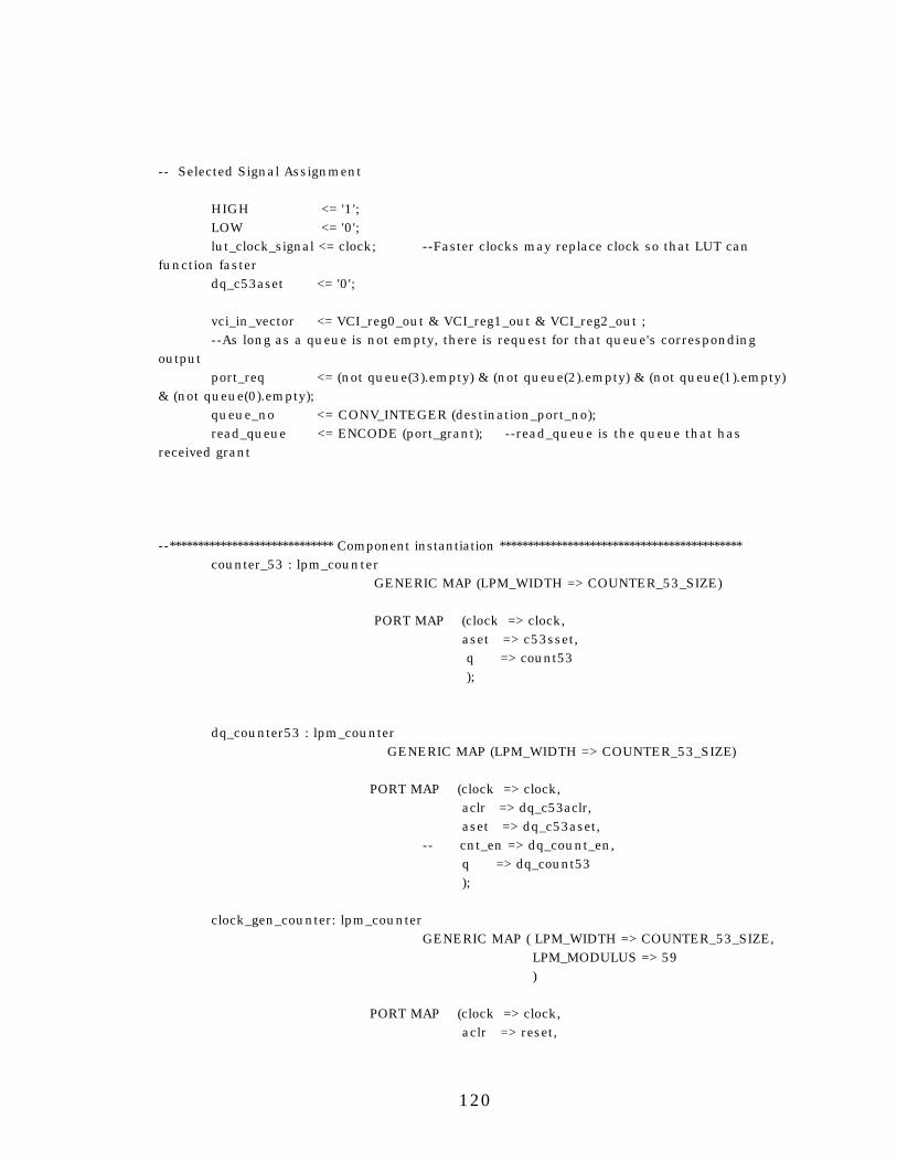
120
-- Selected Signal Assignment HIGH <= '1'; LOW <= '0'; lut_clock_signal <= clock; --Faster clocks may replace clock so that LUT can function faster dq_c53aset <= '0'; vci_in_vector <= VCI_reg0_out & VCI_reg1_out & VCI_reg2_out ; --As long as a queue is not empty, there is request for that queue's corresponding output port_req <= (not queue(3).empty) & (not queue(2).empty) & (not queue(1).empty) & (not queue(0).empty); queue_no <= CONV_INTEGER (destination_port_no); read_queue <= ENCODE (port_grant); --read_queue is the queue that has received grant --***************************** Component instantiation ******************************************* counter_53 : lpm_counter GENERIC MAP (LPM_WIDTH => COUNTER_53_SIZE) PORT MAP (clock => clock, aset => c53sset, q => count53 ); dq_counter53 : lpm_counter GENERIC MAP (LPM_WIDTH => COUNTER_53_SIZE) PORT MAP (clock => clock, aclr => dq_c53aclr, aset => dq_c53aset, -- cnt_en => dq_count_en, q => dq_count53 ); clock_gen_counter: lpm_counter GENERIC MAP ( LPM_WIDTH => COUNTER_53_SIZE, LPM_MODULUS => 59 ) PORT MAP (clock => clock, aclr => reset,
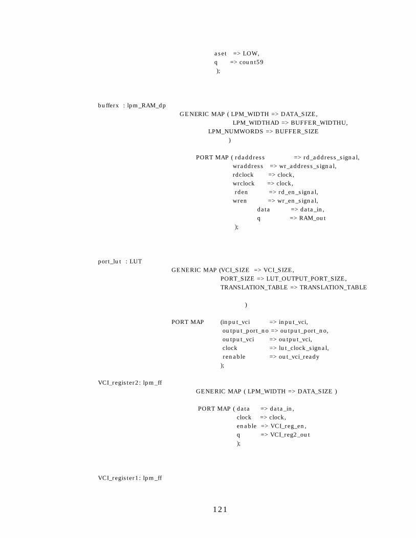
121
aset => LOW, q => count59 ); bufferx : lpm_RAM_dp GENERIC MAP ( LPM_WIDTH => DATA_SIZE, LPM_WIDTHAD => BUFFER_WIDTHU, LPM_NUMWORDS => BUFFER_SIZE ) PORT MAP ( rdaddress => rd_address_signal, wraddress => wr_address_signal, rdclock => clock, wrclock => clock,
rden => rd_en_signal, wren => wr_en_signal,
data => data_in, q => RAM_out ); port_lut : LUT GENERIC MAP (VCI_SIZE => VCI_SIZE, PORT_SIZE => LUT_OUTPUT_PORT_SIZE, TRANSLATION_TABLE => TRANSLATION_TABLE ) PORT MAP (input_vci => input_vci, output_port_no => output_port_no, output_vci => output_vci, clock => lut_clock_signal, renable => out_vci_ready ); VCI_register2: lpm_ff GENERIC MAP ( LPM_WIDTH => DATA_SIZE ) PORT MAP ( data => data_in, clock => clock, enable => VCI_reg_en, q => VCI_reg2_out ); VCI_register1: lpm_ff
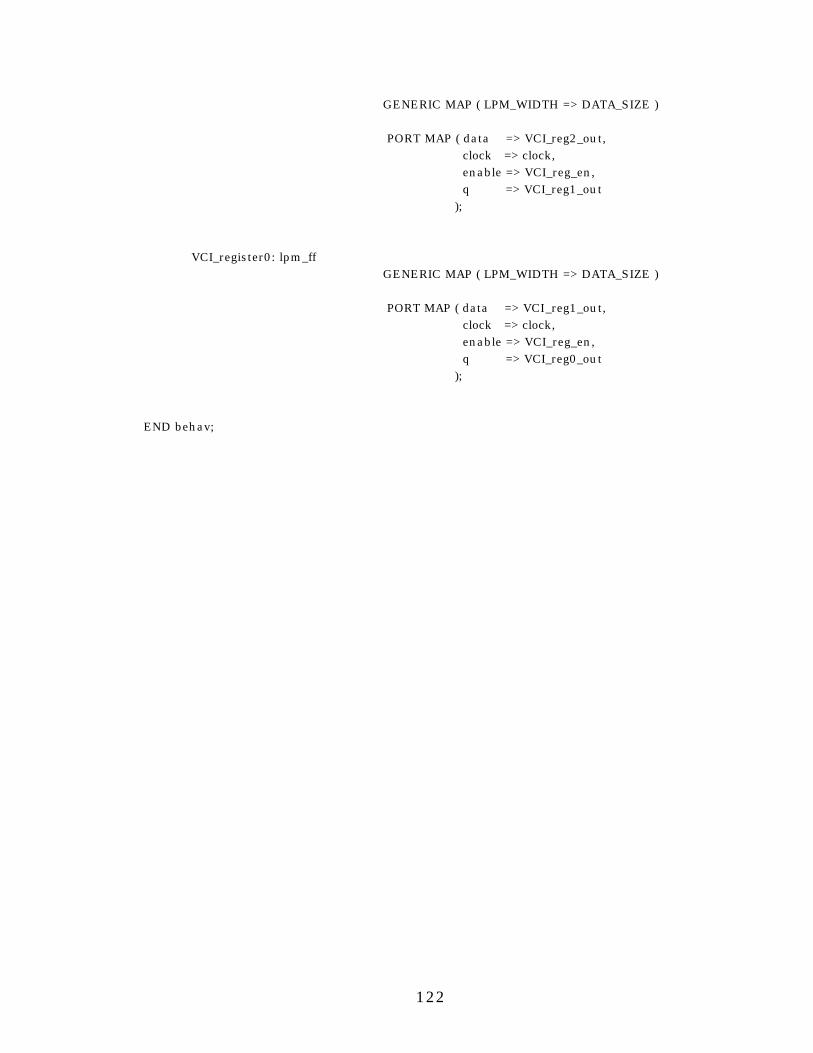
122
GENERIC MAP ( LPM_WIDTH => DATA_SIZE ) PORT MAP ( data => VCI_reg2_out, clock => clock, enable => VCI_reg_en, q => VCI_reg1_out ); VCI_register0: lpm_ff GENERIC MAP ( LPM_WIDTH => DATA_SIZE ) PORT MAP ( data => VCI_reg1_out, clock => clock, enable => VCI_reg_en, q => VCI_reg0_out ); END behav;
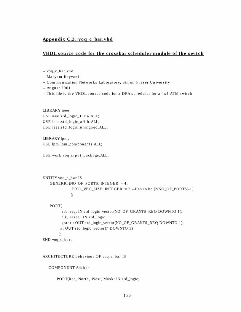
123
Appendix C.3. voq_c_bar.vhd
VHDL source code for the crossbar scheduler module of the switch -- voq_c_bar.vhd -- Maryam Keyvani -- Communication Networks Laboratory, Simon Fraser University -- August 2001 -- This file is the VHDL source code for a DPA scheduler for a 4x4 ATM switch LIBRARY ieee; USE ieee.std_logic_1164.ALL; USE ieee.std_logic_arith.ALL; USE ieee.std_logic_unsigned.ALL; LIBRARY lpm; USE lpm.lpm_components.ALL; USE work.voq_input_package.ALL; ENTITY voq_c_bar IS GENERIC (NO_OF_PORTS: INTEGER := 4; PRIO_VEC_SIZE: INTEGER := 7 --Has to be [2(NO_OF_PORTS)-1] ); PORT(
arb_req: IN std_logic_vector(NO_OF_GRANTS_REQ DOWNTO 1); clk, reset : IN std_logic; grant : OUT std_logic_vector(NO_OF_GRANTS_REQ DOWNTO 1); P: OUT std_logic_vector(7 DOWNTO 1) ); END voq_c_bar; ARCHITECTURE behaviour OF voq_c_bar IS COMPONENT Arbiter PORT(Req, North, West, Mask: IN std_logic;
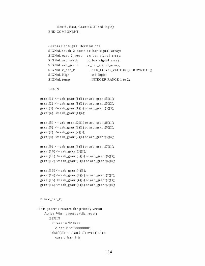
124
South, East, Grant: OUT std_logic); END COMPONENT; --Cross Bar Signal Declarations SIGNAL south_2_north : c_bar_signal_array; SIGNAL east_2_west : c_bar_signal_array; SIGNAL arb_mask : c_bar_signal_array; SIGNAL arb_grant : c_bar_signal_array; SIGNAL c_bar_P : STD_LOGIC_VECTOR (7 DOWNTO 1); SIGNAL High : std_logic; SIGNAL temp : INTEGER RANGE 1 to 2; BEGIN grant(1) <= arb_grant(1)(1) or arb_grant(5)(1); grant(2) <= arb_grant(1)(2) or arb_grant(5)(2); grant(3) <= arb_grant(1)(3) or arb_grant(5)(3); grant(4) <= arb_grant(1)(4); grant(5) <= arb_grant(2)(1) or arb_grant(6)(1); grant(6) <= arb_grant(2)(2) or arb_grant(6)(2); grant(7) <= arb_grant(2)(3); grant(8) <= arb_grant(2)(4) or arb_grant(5)(4); grant(9) <= arb_grant(3)(1) or arb_grant(7)(1); grant(10) <= arb_grant(3)(2); grant(11) <= arb_grant(3)(3) or arb_grant(6)(3); grant(12) <= arb_grant(3)(4) or arb_grant(6)(4); grant(13) <= arb_grant(4)(1); grant(14) <= arb_grant(4)(2) or arb_grant(7)(2); grant(15) <= arb_grant(4)(3) or arb_grant(7)(3); grant(16) <= arb_grant(4)(4) or arb_grant(7)(4); P <= c_bar_P; --This process rotates the priority vector Active_Win : process (clk, reset) BEGIN if reset = '0' then c_bar_P <= "0000000"; elsif (clk = '1' and clk'event) then case c_bar_P is
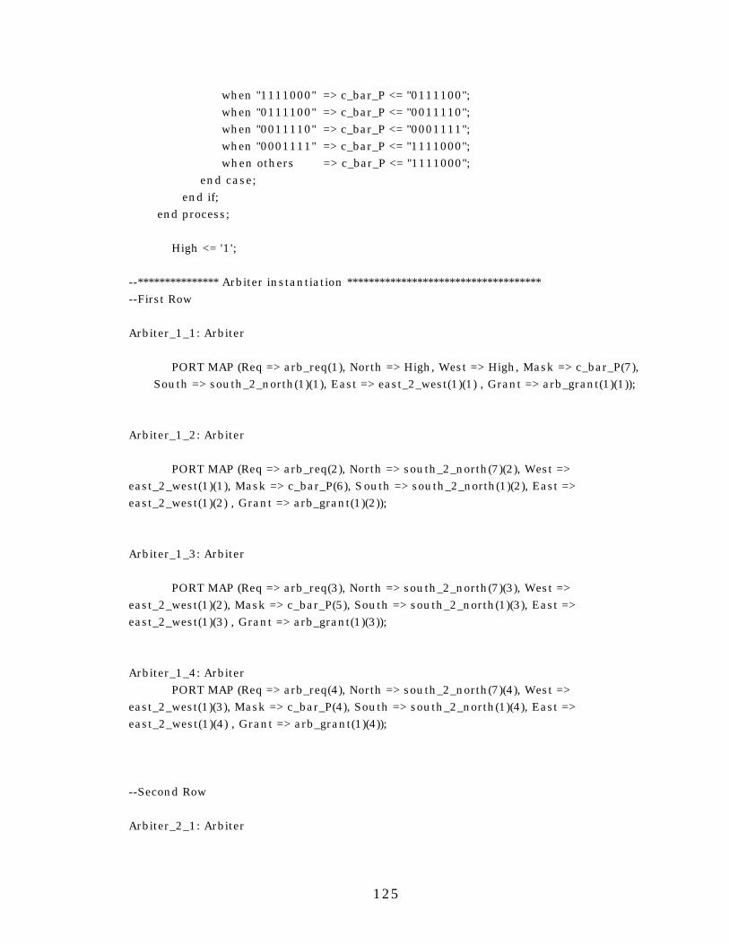
125
when "1111000" => c_bar_P <= "0111100"; when "0111100" => c_bar_P <= "0011110"; when "0011110" => c_bar_P <= "0001111"; when "0001111" => c_bar_P <= "1111000"; when others => c_bar_P <= "1111000"; end case; end if; end process; High <= '1'; --*************** Arbiter instantiation ************************************ --First Row Arbiter_1_1: Arbiter
PORT MAP (Req => arb_req(1), North => High, West => High, Mask => c_bar_P(7), South => south_2_north(1)(1), East => east_2_west(1)(1) , Grant => arb_grant(1)(1)); Arbiter_1_2: Arbiter PORT MAP (Req => arb_req(2), North => south_2_north(7)(2), West => east_2_west(1)(1), Mask => c_bar_P(6), South => south_2_north(1)(2), East => east_2_west(1)(2) , Grant => arb_grant(1)(2)); Arbiter_1_3: Arbiter PORT MAP (Req => arb_req(3), North => south_2_north(7)(3), West => east_2_west(1)(2), Mask => c_bar_P(5), South => south_2_north(1)(3), East => east_2_west(1)(3) , Grant => arb_grant(1)(3)); Arbiter_1_4: Arbiter PORT MAP (Req => arb_req(4), North => south_2_north(7)(4), West => east_2_west(1)(3), Mask => c_bar_P(4), South => south_2_north(1)(4), East => east_2_west(1)(4) , Grant => arb_grant(1)(4)); --Second Row Arbiter_2_1: Arbiter
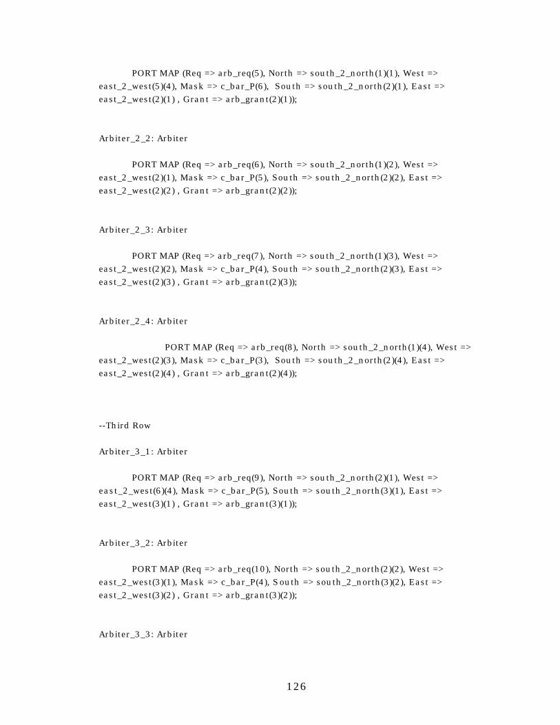
126
PORT MAP (Req => arb_req(5), North => south_2_north(1)(1), West => east_2_west(5)(4), Mask => c_bar_P(6), South => south_2_north(2)(1), East => east_2_west(2)(1) , Grant => arb_grant(2)(1)); Arbiter_2_2: Arbiter PORT MAP (Req => arb_req(6), North => south_2_north(1)(2), West => east_2_west(2)(1), Mask => c_bar_P(5), South => south_2_north(2)(2), East => east_2_west(2)(2) , Grant => arb_grant(2)(2)); Arbiter_2_3: Arbiter PORT MAP (Req => arb_req(7), North => south_2_north(1)(3), West => east_2_west(2)(2), Mask => c_bar_P(4), South => south_2_north(2)(3), East => east_2_west(2)(3) , Grant => arb_grant(2)(3)); Arbiter_2_4: Arbiter PORT MAP (Req => arb_req(8), North => south_2_north(1)(4), West => east_2_west(2)(3), Mask => c_bar_P(3), South => south_2_north(2)(4), East => east_2_west(2)(4) , Grant => arb_grant(2)(4)); --Third Row Arbiter_3_1: Arbiter PORT MAP (Req => arb_req(9), North => south_2_north(2)(1), West => east_2_west(6)(4), Mask => c_bar_P(5), South => south_2_north(3)(1), East => east_2_west(3)(1) , Grant => arb_grant(3)(1)); Arbiter_3_2: Arbiter PORT MAP (Req => arb_req(10), North => south_2_north(2)(2), West => east_2_west(3)(1), Mask => c_bar_P(4), South => south_2_north(3)(2), East => east_2_west(3)(2) , Grant => arb_grant(3)(2)); Arbiter_3_3: Arbiter
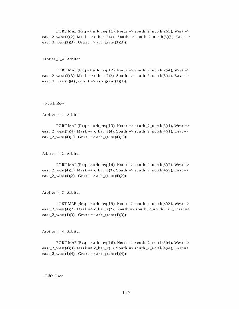
127
PORT MAP (Req => arb_req(11), North => south_2_north(2)(3), West => east_2_west(3)(2), Mask => c_bar_P(3), South => south_2_north(3)(3), East => east_2_west(3)(3) , Grant => arb_grant(3)(3)); Arbiter_3_4: Arbiter PORT MAP (Req => arb_req(12), North => south_2_north(2)(4), West => east_2_west(3)(3), Mask => c_bar_P(2), South => south_2_north(3)(4), East => east_2_west(3)(4) , Grant => arb_grant(3)(4)); --Forth Row Arbiter_4_1: Arbiter PORT MAP (Req => arb_req(13), North => south_2_north(3)(1), West => east_2_west(7)(4), Mask => c_bar_P(4), South => south_2_north(4)(1), East => east_2_west(4)(1) , Grant => arb_grant(4)(1)); Arbi ter_4_2: Arbiter PORT MAP (Req => arb_req(14), North => south_2_north(3)(2), West => east_2_west(4)(1), Mask => c_bar_P(3), South => south_2_north(4)(2), East => east_2_west(4)(2) , Grant => arb_grant(4)(2)); Arbiter_4_3: Arbiter PORT MAP (Req => arb_req(15), North => south_2_north(3)(3), West => east_2_west(4)(2), Mask => c_bar_P(2), South => south_2_north(4)(3), East => east_2_west(4)(3) , Grant => arb_grant(4)(3)); Arbiter_4_4: Arbiter PORT MAP (Req => arb_req(16), North => south_2_north(3)(4), West => east_2_west(4)(3), Mask => c_bar_P(1), South => south_2_north(4)(4), East => east_2_west(4)(4) , Grant => arb_grant(4)(4)); --Fifth Row
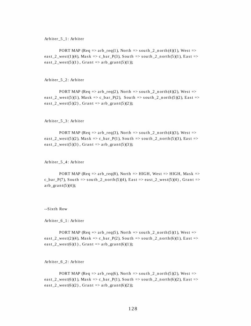
128
Arbiter_5_1: Arbiter PORT MAP (Req => arb_req(1), North => south_2_north(4)(1), West => east_2_west(1)(4), Mask => c_bar_P(3), South => south_2_north(5)(1), East => east_2_west(5)(1) , Grant => arb_grant(5)(1)); Arbiter_5_2: Arbiter PORT MAP (Req => arb_req(2), North => south_2_north(4)(2), West => east_2_west(5)(1), Mask => c_bar_P(2), South => south_2_north(5)(2), East => east_2_west(5)(2) , Grant => arb_grant(5)(2)); Arbiter_5_3: Arbiter PORT MAP (Req => arb_req(3), North => south_2_north(4)(3), West => east_2_west(5)(2), Mask => c_bar_P(1), South => south_2_north(5)(3), East => east_2_west(5)(3) , Grant => arb_grant(5)(3)); Arbiter_5_4: Arbiter PORT MAP (Req => arb_req(8), North => HIGH, West => HIGH, Mask => c_bar_P(7), South => south_2_north(5)(4), East => east_2_west(5)(4) , Grant => arb_grant(5)(4)); --Sixth Row Arbiter_6_1: Arbiter PORT MAP (Req => arb_req(5), North => south_2_north(5)(1), West => east_2_west(2)(4), Mask => c_bar_P(2), South => south_2_north(6)(1), East => east_2_west(6)(1) , Grant => arb_grant(6)(1)); Arbiter_6_2: Arbiter PORT MAP (Req => arb_req(6), North => south_2_north(5)(2), West => east_2_west(6)(1), Mask => c_bar_P(1), South => south_2_north(6)(2), East => east_2_west(6)(2) , Grant => arb_grant(6)(2));
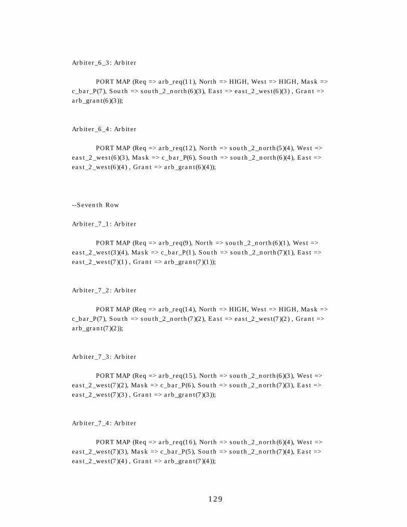
129
Arbiter_6_3: Arbiter PORT MAP (Req => arb_req(11), North => HIGH, West => HIGH, Mask => c_bar_P(7), South => south_2_north(6)(3), East => east_2_west(6)(3) , Grant => arb_grant(6)(3)); Arbiter_6_4: Arbiter
PORT MAP (Req => arb_req(12), North => south_2_north(5)(4), West => east_2_west(6)(3), Mask => c_bar_P(6), South => south_2_north(6)(4), East => east_2_west(6)(4) , Grant => arb_grant(6)(4)); --Seventh Row Arbiter_7_1: Arbiter PORT MAP (Req => arb_req(9), North => south_2_north(6)(1), West => east_2_west(3)(4), Mask => c_bar_P(1), South => south_2_north(7)(1), East => east_2_west(7)(1) , Grant => arb_grant(7)(1)); Arbiter_7_2: Arbiter PORT MAP (Req => arb_req(14), North => HIGH, West => HIGH, Mask => c_bar_P(7), South => south_2_north(7)(2), East => east_2_west(7)(2) , Grant => arb_grant(7)(2)); Arbiter_7_3: Arbiter PORT MAP (Req => arb_req(15), North => south_2_north(6)(3), West => east_2_west(7)(2), Mask => c_bar_P(6), South => south_2_north(7)(3), East => east_2_west(7)(3) , Grant => arb_grant(7)(3)); Arbiter_7_4: Arbiter PORT MAP (Req => arb_req(16), North => south_2_north(6)(4), West => east_2_west(7)(3), Mask => c_bar_P(5), South => south_2_north(7)(4), East => east_2_west(7)(4) , Grant => arb_grant(7)(4));
130
END behaviour;
131
Appendix C.4. voq_fabric.vhd
VHLD source code for the crossbar fabric module of the switch
-- voq_fabric.vhd -- Designed by: Maryam Keyvani -- Communication Networks Lab, Simon Fraser University -- August 2001 -- This is a crossbar fabric made from AND gates and OR gates -- The control lines of the fabric come from the size 16 std_logic_vector -- input "cntrl", which is in this case the "grant" signal comming from the scheduler. LIBRARY ieee; USE ieee.std_logic_1164.ALL; USE ieee.std_logic_arith.ALL; LIBRARY lpm; USE lpm.lpm_components.ALL; USE work.voq_input_package.ALL; ENTITY voq_fabric is GENERIC( SWITCH_SIZE : INTEGER:= 4; --4x4 fabric by default GRANT_SIZE : INTEGER:= 16 --16 lines used to issue grants ); PORT( input0 : IN DATA_VECTOR; --The 4 input data lines of type std_logic_vector(DATASIZE-1 DOWNTO 0) input1 : IN STD_LOGIC_VECTOR(SWITCH_SIZE-1 DOWNTO 0); --The 4 data_valid lines going to the fabric input2 : IN STD_LOGIC_VECTOR(SWITCH_SIZE-1 DOWNTO 0); --The LSBs of input_port_name input3 : IN STD_LOGIC_VECTOR(SWITCH_SIZE-1 DOWNTO 0); --The MSB bit of input_port_name
input4 : IN STD_LOGIC_VECTOR(SWITCH_SIZE-1 DOWNTO 0); --The 4 input frame pulse lines
132
cntrl : IN STD_LOGIC_VECTOR(GRANT_SIZE-1 DOWNTO 0); --The grant vector used to control the fabric output0 : OUT DATA_VECTOR; --The 4 output data lines of type std_logic_vecotr(DATASIZE-1 DOWNTO 0) output1 : OUT STD_LOGIC_VECTOR(SWITCH_SIZE-1 DOWNTO 0); --data_valid lines output2 : OUT STD_LOGIC_VECTOR(SWITCH_SIZE-1 DOWNTO 0); --The LSBs of port_name out of the fabric output3 : OUT STD_LOGIC_VECTOR(SWITCH_SIZE-1 DOWNTO 0); --The MSB of port_name out of the fabric output4 : OUT STD_LOGIC_VECTOR(SWITCH_SIZE-1 DOWNTO 0) --the 4 output frame pulses for the 8 output ports ); END voq_fabric; Architecture behave of voq_fabric is
begin output0(0)(0) <= ( (input0(0)(0) AND cntrl(0)) OR (input0(1)(0) AND cntrl(4)) OR (input0(2)(0) AND cntrl(8)) OR (input0(3)(0) AND cntrl(12)) ); output0(0)(1) <= ( (input0(0)(1) AND cntrl(0)) OR (input0(1)(1) AND cntrl(4)) OR (input0(2)(1) AND cntrl(8)) OR (input0(3)(1) AND cntrl(12)) ); output0(0)(2) <= ( (input0(0)(2) AND cntrl(0)) OR (input0(1)(2) AND cntrl(4)) OR (input0(2)(2) AND cntrl(8)) OR (input0(3)(2) AND cntrl(12)) ); output0(0)(3) <= ( (input0(0)(3) AND cntrl(0)) OR (input0(1)(3) AND cntrl(4)) OR (input0(2)(3) AND cntrl(8)) OR (input0(3)(3) AND cntrl(12)) ); output0(0)(4) <= ( (input0(0)(4) AND cntrl(0)) OR (input0(1)(4) AND cntrl(4)) OR (input0(2)(4) AND cntrl(8)) OR (input0(3)(4) AND cntrl(12)) ); output0(0)(5) <= ( (input0(0)(5) AND cntrl(0)) OR (input0(1)(5) AND cntrl(4)) OR (input0(2)(5) AND cntrl(8)) OR (input0(3)(5) AND cntrl(12))); output0(0)(6) <= ( (input0(0)(6) AND cntrl(0)) OR (input0(1)(6) AND cntrl(4)) OR (input0(2)(6) AND cntrl(8)) OR (input0(3)(6) AND cntrl(12)));
133
output0(0)(7) <= ( (input0(0)(7) AND cntrl(0)) OR (input0(1)(7) AND cntrl(4)) OR (input0(2)(7) AND cntrl(8)) OR (input0(3)(7) AND cntrl(12))); output0(1)(0) <= ( (input0(0)(0) AND cntrl(1)) OR (input0(1)(0) AND cntrl(5)) OR (input0(2)(0) AND cntrl(9)) OR (input0(3)(0) AND cntrl(13))); output0(1)(1) <= ( (input0(0)(1) AND cntrl(1)) OR (input0(1)(1) AND cntrl(5)) OR (input0(2)(1) AND cntrl(9)) OR (input0(3)(1) AND cntrl(13))); output0(1)(2) <= ( (input0(0)(2) AND cntrl(1)) OR (input0(1)(2) AND cntrl(5)) OR (input0(2)(2) AND cntrl(9)) OR (input0(3)(2) AND cntrl(13))); output0(1)(3) <= ( (input0(0)(3) AND cntrl(1)) OR (input0(1)(3) AND cntrl(5)) OR (input0(2)(3) AND cntrl(9)) OR (input0(3)(3) AND cntrl(13))); output0(1)(4) <= ( (input0(0)(4) AND cntrl(1)) OR (input0(1)(4) AND cntrl(5)) OR (input0(2)(4) AND cntrl(9)) OR (input0(3)(4) AND cntrl(13))); output0(1)(5) <= ( (input0(0)(5) AND cntrl(1)) OR (input0(1)(5) AND cntrl(5)) OR (input0(2)(5) AND cntrl(9)) OR (input0(3)(5) AND cntrl(13))); output0(1)(6) <= ( (input0(0)(6) AND cntrl(1)) OR (input0(1)(6) AND cntrl(5)) OR (input0(2)(6) AND cntrl(9)) OR (input0(3)(6) AND cntrl(13))); output0(1)(7) <= ( (input0(0)(7) AND cntrl(1)) OR (input0(1)(7) AND cntrl(5)) OR (input0(2)(7) AND cntrl(9)) OR (input0(3)(7) AND cntrl(13))); output0(2)(0) <= ( (input0(0)(0) AND cntrl(2)) OR (input0(1)(0) AND cntrl(6)) OR (input0(2)(0) AND cntrl(10)) OR (input0(3)(0) AND cntrl(14))); output0(2)(1) <= ( (input0(0)(1) AND cntrl(2)) OR (input0(1)(1) AND cntrl(6)) OR (input0(2)(1) AND cntrl(10)) OR (input0(3)(1) AND cntrl(14))); output0(2)(2) <= ( (input0(0)(2) AND cntrl(2)) OR (input0(1)(2) AND cntrl(6)) OR (input0(2)(2) AND cntrl(10)) OR (input0(3)(2) AND cntrl(14)));
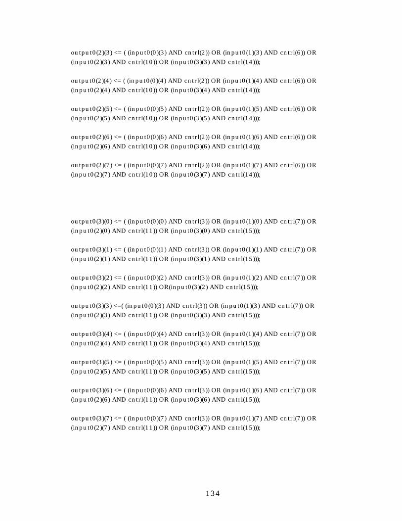
134
output0(2)(3) <= ( (input0(0)(3) AND cntrl(2)) OR (input0(1)(3) AND cntrl(6)) OR (input0(2)(3) AND cntrl(10)) OR (input0(3)(3) AND cntrl(14))); output0(2)(4) <= ( (input0(0)(4) AND cntrl(2)) OR (input0(1)(4) AND cntrl(6)) OR (input0(2)(4) AND cntrl(10)) OR (input0(3)(4) AND cntrl(14))); output0(2)(5) <= ( (input0(0)(5) AND cntrl(2)) OR (input0(1)(5) AND cntrl(6)) OR (input0(2)(5) AND cntrl(10)) OR (input0(3)(5) AND cntrl(14))); output0(2)(6) <= ( (input0(0)(6) AND cntrl(2)) OR (input0(1)(6) AND cntrl(6)) OR (input0(2)(6) AND cntrl(10)) OR (input0(3)(6) AND cntrl(14))); output0(2)(7) <= ( (input0(0)(7) AND cntrl(2)) OR (input0(1)(7) AND cntrl(6)) OR (input0(2)(7) AND cntrl(10)) OR (input0(3)(7) AND cntrl(14))); output0(3)(0) <= ( (input0(0)(0) AND cntrl(3)) OR (input0(1)(0) AND cntrl(7)) OR (input0(2)(0) AND cntrl(11)) OR (input0(3)(0) AND cntrl(15))); output0(3)(1) <= ( (input0(0)(1) AND cntrl(3)) OR (input0(1)(1) AND cntrl(7)) OR (input0(2)(1) AND cntrl(11)) OR (input0(3)(1) AND cntrl(15))); output0(3)(2) <= ( (input0(0)(2) AND cntrl(3)) OR (input0(1)(2) AND cntrl(7)) OR (input0(2)(2) AND cntrl(11)) OR(input0(3)(2) AND cntrl(15))); output0(3)(3) <=( (input0(0)(3) AND cntrl(3)) OR (input0(1)(3) AND cntrl(7)) OR (input0(2)(3) AND cntrl(11)) OR (input0(3)(3) AND cntrl(15))); output0(3)(4) <= ( (input0(0)(4) AND cntrl(3)) OR (input0(1)(4) AND cntrl(7)) OR (input0(2)(4) AND cntrl(11)) OR (input0(3)(4) AND cntrl(15))); output0(3)(5) <= ( (input0(0)(5) AND cntrl(3)) OR (input0(1)(5) AND cntrl(7)) OR (input0(2)(5) AND cntrl(11)) OR (input0(3)(5) AND cntrl(15))); output0(3)(6) <= ( (input0(0)(6) AND cntrl(3)) OR (input0(1)(6) AND cntrl(7)) OR (input0(2)(6) AND cntrl(11)) OR (input0(3)(6) AND cntrl(15))); output0(3)(7) <= ( (input0(0)(7) AND cntrl(3)) OR (input0(1)(7) AND cntrl(7)) OR (input0(2)(7) AND cntrl(11)) OR (input0(3)(7) AND cntrl(15)));
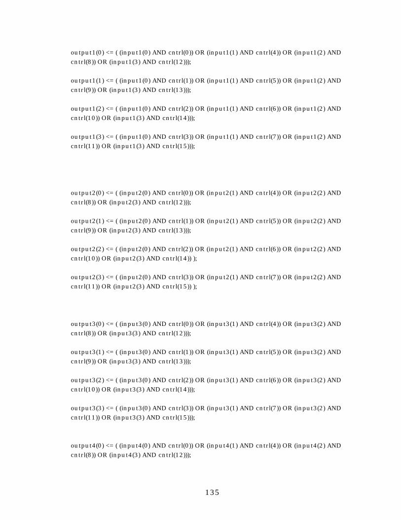
135
output1(0) <= ( (input1(0) AND cntrl(0)) OR (input1(1) AND cntrl(4)) OR (input1(2) AND cntrl(8)) OR (input1(3) AND cntrl(12))); output1(1) <= ( (input1(0) AND cntrl(1)) OR (input1(1) AND cntrl(5)) OR (input1(2) AND cntrl(9)) OR (input1(3) AND cntrl(13))); output1(2) <= ( (input1(0) AND cntrl(2)) OR (input1(1) AND cntrl(6)) OR (input1(2) AND cntrl(10)) OR (input1(3) AND cntrl(14))); output1(3) <= ( (input1(0) AND cntrl(3)) OR (input1(1) AND cntrl(7)) OR (input1(2) AND cntrl(11)) OR (input1(3) AND cntrl(15))); output2(0) <= ( (input2(0) AND cntrl(0)) OR (input2(1) AND cntrl(4)) OR (input2(2) AND cntrl(8)) OR (input2(3) AND cntrl(12))); output2(1) <= ( (input2(0) AND cntrl(1)) OR (input2(1) AND cntrl(5)) OR (input2(2) AND cntrl(9)) OR (input2(3) AND cntrl(13))); output2(2) <= ( (input2(0) AND cntrl(2)) OR (input2(1) AND cntrl(6)) OR (input2(2) AND cntrl(10)) OR (input2(3) AND cntrl(14)) ); output2(3) <= ( (input2(0) AND cntrl(3)) OR (input2(1) AND cntrl(7)) OR (input2(2) AND cntrl(11)) OR (input2(3) AND cntrl(15)) ); output3(0) <= ( (input3(0) AND cntrl(0)) OR (input3(1) AND cntrl(4)) OR (input3(2) AND cntrl(8)) OR (input3(3) AND cntrl(12))); output3(1) <= ( (input3(0) AND cntrl(1)) OR (input3(1) AND cntrl(5)) OR (input3(2) AND cntrl(9)) OR (input3(3) AND cntrl(13))); output3(2) <= ( (input3(0) AND cntrl(2)) OR (input3(1) AND cntrl(6)) OR (input3(2) AND cntrl(10)) OR (input3(3) AND cntrl(14))); output3(3) <= ( (input3(0) AND cntrl(3)) OR (input3(1) AND cntrl(7)) OR (input3(2) AND cntrl(11)) OR (input3(3) AND cntrl(15))); output4(0) <= ( (input4(0) AND cntrl(0)) OR (input4(1) AND cntrl(4)) OR (input4(2) AND cntrl(8)) OR (input4(3) AND cntrl(12)));
136
output4(1) <= ( (input4(0) AND cntrl(1)) OR (input4(1) AND cntrl(5)) OR (input4(2) AND cntrl(9)) OR (input4(3) AND cntrl(13))); output4(2) <= ( (input4(0) AND cntrl(2)) OR (input4(1) AND cntrl(6)) OR (input4(2) AND cntrl(10)) OR (input4(3) AND cntrl(14))); output4(3) <= ( (input4(0) AND cntrl(3)) OR (input4(1) AND cntrl(7)) OR (input4(2) AND cntrl(11)) OR (input4(3) AND cntrl(15))); end behave;
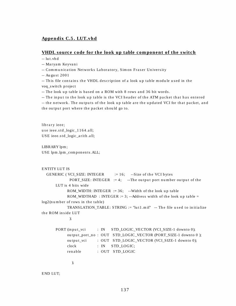
137
Appendix C.5. LUT.vhd
VHDL source code for the look up table component of the switch -- lut.vhd -- Maryam Keyvani -- Communication Networks Laboratory, Simon Fraser University -- August 2001 -- This file contains the VHDL description of a look up table module used in the voq_switch project -- The look up table is based on a ROM with 8 rows and 36 bit words. -- The input to the look up table is the VCI header of the ATM packet that has entered -- the network. The outputs of the look up table are the updated VCI for that packet, and the output port where the packet should go to. library ieee; use ieee.std_logic_1164.all; USE ieee.std_logic_arith.all; LIBRARY lpm; USE lpm.lpm_components.ALL; ENTITY LUT IS GENERIC ( VCI_SIZE: INTEGER := 16; --Size of the VCI bytes
PORT_SIZE: INTEGER := 4; --The output port number output of the LUT is 4 bits wide
ROM_WIDTH: INTEGER := 36; --Width of the look up table ROM_WIDTHAD : INTEGER := 3; --Address width of the look up table = log2(number of rows in the table) TRANSLATION_TABLE: STRING := "lut1.mif" -- The file used to initialize the ROM inside LUT ); PORT (input_vci : IN STD_LOGIC_VECTOR (VCI_SIZE-1 downto 0); output_port_no : OUT STD_LOGIC_VECTOR (PORT_SIZE-1 downto 0 ); output_vci : OUT STD_LOGIC_VECTOR (VCI_SIZE-1 downto 0); clock : IN STD_LOGIC; renable : OUT STD_LOGIC ); END LUT;
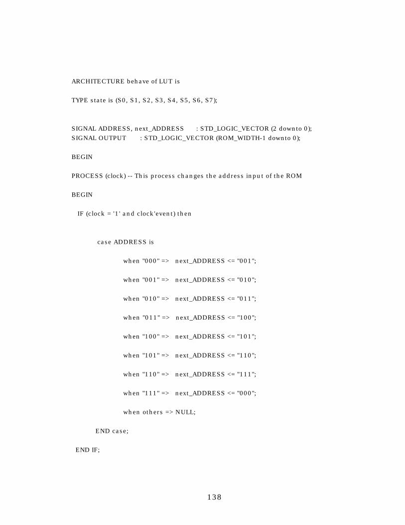
138
ARCHITECTURE behave of LUT is TYPE state is (S0, S1, S2, S3, S4, S5, S6, S7); SIGNAL ADDRESS, next_ADDRESS : STD_LOGIC_VECTOR (2 downto 0); SIGNAL OUTPUT : STD_LOGIC_VECTOR (ROM_WIDTH-1 downto 0); BEGIN PROCESS (clock) -- This process changes the address input of the ROM BEGIN IF (clock = '1' and clock'event) then case ADDRESS is when "000" => next_ADDRESS <= "001"; when "001" => next_ADDRESS <= "010"; when "010" => next_ADDRESS <= "011"; when "011" => next_ADDRESS <= "100"; when "100" => next_ADDRESS <= "101"; when "101" => next_ADDRESS <= "110"; when "110" => next_ADDRESS <= "111"; when "111" => next_ADDRESS <= "000"; when others => NULL; END case; END IF;
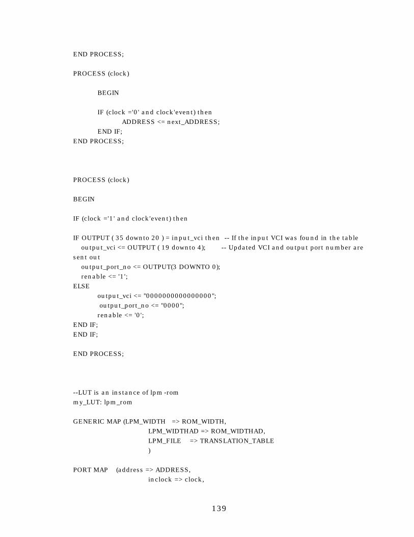
139
END PROCESS; PROCESS (clock) BEGIN IF (clock ='0' and clock'event) then ADDRESS <= next_ADDRESS; END IF; END PROCESS; PROCESS (clock) BEGIN IF (clock ='1' and clock'event) then IF OUTPUT ( 35 downto 20 ) = input_vci then -- If the input VCI was found in the table output_vci <= OUTPUT ( 19 downto 4); -- Updated VCI and output port number are sent out output_port_no <= OUTPUT(3 DOWNTO 0); renable <= '1'; ELSE output_vci <= "0000000000000000"; output_port_no <= "0000"; renable <= '0'; END IF; END IF; END PROCESS; --LUT is an instance of lpm -rom my_LUT: lpm_rom GENERIC MAP (LPM_WIDTH => ROM_WIDTH, LPM_WIDTHAD => ROM_WIDTHAD, LPM_FILE => TRANSLATION_TABLE ) PORT MAP (address => ADDRESS, inclock => clock,
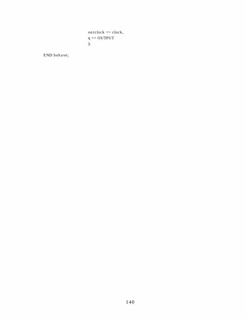
140
outclock => clock, q => OUTPUT ); END behave;
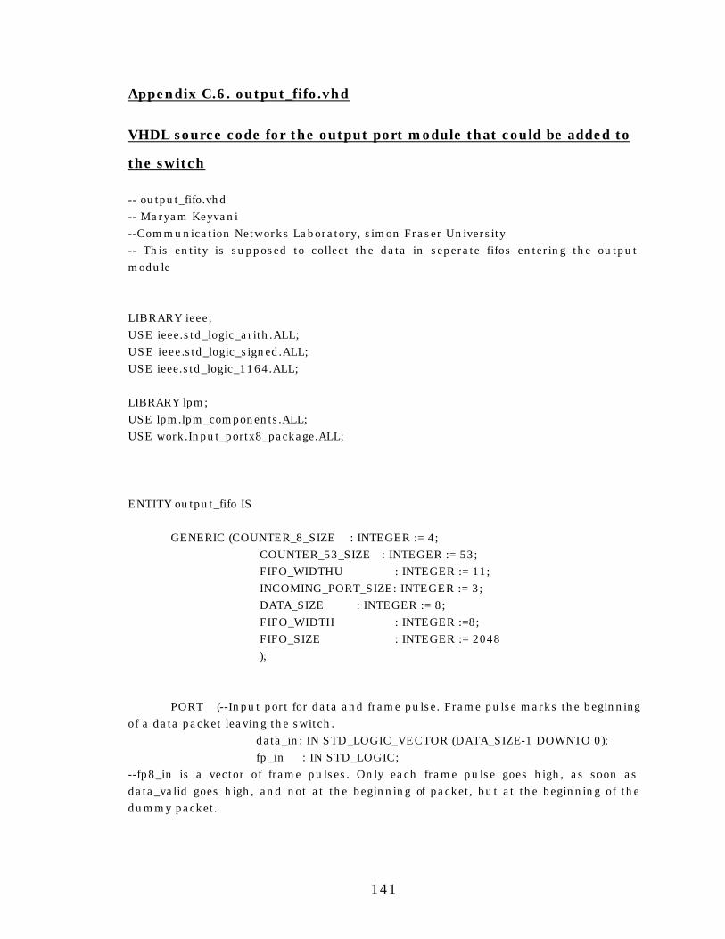
141
Appendix C.6. output_fifo.vhd
VHDL source code for the output port module that could be added to
the switch -- output_fifo.vhd -- Maryam Keyvani --Communication Networks Laboratory, simon Fraser University -- This entity is supposed to collect the data in seperate fifos entering the output module LIBRARY ieee; USE ieee.std_logic_arith.ALL; USE ieee.std_logic_signed.ALL; USE ieee.std_logic_1164.ALL; LIBRARY lpm; USE lpm.lpm_components.ALL; USE work.Input_portx8_package.ALL; ENTITY output_fifo IS GENERIC (COUNTER_8_SIZE : INTEGER := 4; COUNTER_53_SIZE : INTEGER := 53; FIFO_WIDTHU : INTEGER := 11; INCOMING_PORT_SIZE: INTEGER := 3; DATA_SIZE : INTEGER := 8; FIFO_WIDTH : INTEGER :=8; FIFO_SIZE : INTEGER := 2048 ); PORT (--Input port for data and frame pulse. Frame pulse marks the beginning of a data packet leaving the switch. data_in: IN STD_LOGIC_VECTOR (DATA_SIZE-1 DOWNTO 0); fp_in : IN STD_LOGIC; --fp8_in is a vector of frame pulses. Only each frame pulse goes high, as soon as data_valid goes high, and not at the beginning of packet, but at the beginning of the dummy packet.
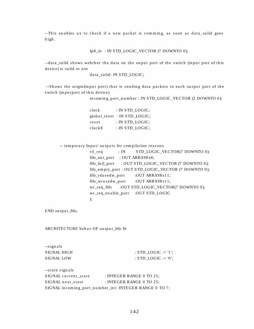
142
--This enables us to check if a new packet is comming, as soon as data_valid goes high.
fp8_in : IN STD_LOGIC_VECTOR (7 DOWNTO 0); --data_valid shows wehther the data on the ouput port of the switch (input port of this device) is valid or not data_valid: IN STD_LOGIC; --Shows the origin(input port) that is sending data packets to each output port of the switch (inputport of this device) incoming_port_number : IN STD_LOGIC_VECTOR (2 DOWNTO 0); clock : IN STD_LOGIC; global_reset : IN STD_LOGIC; reset : IN STD_LOGIC; clock8 : IN STD_LOGIC; -- temporary Input/outputs for compilation reasons rd_req : IN STD_LOGIC_VECTOR(7 DOWNTO 0); fifo_out_port : OUT ARRAY8x8; fifo_full_port : OUT STD_LOGIC_VECTOR (7 DOWNTO 0); fifo_empty_port : OUT STD_LOGIC_VECTOR (7 DOWNTO 0); fifo_rdusedw_port :OUT ARRAY8x11; fifo_wrusedw_port :OUT ARRAY8x11; wr_req_fifo :OUT STD_LOGIC_VECTOR(7 DOWNTO 0); wr_req_enable_port :OUT STD_LOGIC ); END output_fifo; ARCHITECTURE behav OF output_fifo IS --signals SIGNAL HIGH : STD_LOGIC := '1'; SIGNAL LOW : STD_LOGIC := '0'; --state signals SIGNAL current_state : INTEGER RANGE 0 TO 25; SIGNAL next_state : INTEGER RANGE 0 TO 25; SIGNAL incoming_port_number_int: INTEGER RANGE 0 TO 7;
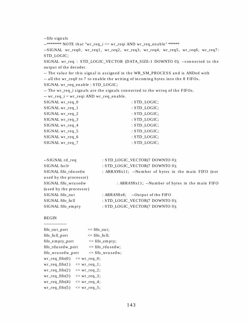
143
--fifo signals --******** NOTE that "wr_req_i <= wr_reqi AND wr_req_enable" ****** --SIGNAL wr_req0, wr_req1, wr_req2, wr_req3, wr_req4, wr_req5, wr_req6, wr_req7: STD_LOGIC; SIGNAL wr_req : STD_LOGIC_VECTOR (DATA_SIZE-1 DOWNTO 0); --connected to the output of the decoder. -- The value for this signal is assigned in the WR_SM_PROCESS and is ANDed with -- all the wr_req0 to 7 to enable the writing of incoming bytes into the 8 FIFOs. SIGNAL wr_req_enable : STD_LOGIC; -- The wr_req_i signals are the signals connected to the wrreq of the FIFOs. -- wr_req_i = wr_reqi AND wr_req_enable. SIGNAL wr_req_0 : STD_LOGIC; SIGNAL wr_req_1 : STD_LOGIC; SIGNAL wr_req_2 : STD_LOGIC; SIGNAL wr_req_3 : STD_LOGIC; SIGNAL wr_req_4 : STD_LOGIC; SIGNAL wr_req_5 : STD_LOGIC; SIGNAL wr_req_6 : STD_LOGIC; SIGNAL wr_req_7 : STD_LOGIC; --SIGNAL rd_req : STD_LOGIC_VECTOR(7 DOWNTO 0); SIGNAL faclr : STD_LOGIC_VECTOR(7 DOWNTO 0); SIGNAL fifo_rdusedw : ARRAY8x11; --Number of bytes in the main FIFO (not used by the processor) SIGNAL fifo_wrusedw : ARRAY8x11; --Number of bytes in the main FIFO (used by the processor) SIGNAL fifo_out : ARRAY8x8; --Output of the FIFO SIGNAL fifo_full : STD_LOGIC_VECTOR(7 DOWNTO 0); SIGNAL fifo_empty : STD_LOGIC_VECTOR(7 DOWNTO 0); BEGIN --------------- fifo_out_port <= fifo_out; fifo_full_port <= fifo_full; fifo_empty_port <= fifo_empty; fifo_rdusedw_port <= fifo_rdusedw; fifo_wrusedw_port <= fifo_wrusedw; wr_req_fifo(0) <= wr_req_0; wr_req_fifo(1) <= wr_req_1; wr_req_fifo(2) <= wr_req_2; wr_req_fifo(3) <= wr_req_3; wr_req_fifo(4) <= wr_req_4; wr_req_fifo(5) <= wr_req_5;
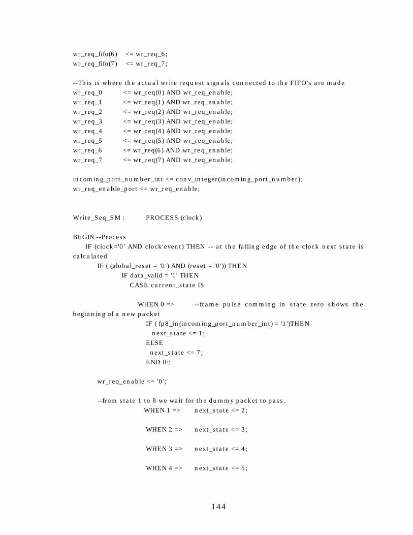
144
wr_req_fifo(6) <= wr_req_6; wr_req_fifo(7) <= wr_req_7; --This is where the actual write request signals connected to the FIFO's are made wr_req_0 <= wr_req(0) AND wr_req_enable; wr_req_1 <= wr_req(1) AND wr_req_enable; wr_req_2 <= wr_req(2) AND wr_req_enable; wr_req_3 <= wr_req(3) AND wr_req_enable; wr_req_4 <= wr_req(4) AND wr_req_enable; wr_req_5 <= wr_req(5) AND wr_req_enable; wr_req_6 <= wr_req(6) AND wr_req_enable; wr_req_7 <= wr_req(7) AND wr_req_enable; incoming_port_number_int <= conv_integer(incoming_port_number); wr_req_enable_port <= wr_req_enable; Write_Seq_SM : PROCESS (clock) BEGIN --Process IF (clock='0' AND clock'event) THEN -- at the falling edge of the clock next state is calculated IF ( (global_reset = '0') AND (reset = '0')) THEN
IF data_valid = '1' THEN CASE current_state IS WHEN 0 => --frame pulse comming in state zero shows the beginning of a new packet IF ( fp8_in(incoming_port_number_int) = '1')THEN
next_state <= 1; ELSE
next_state <= 7; END IF;
wr_req_enable <= '0'; --from state 1 to 8 we wait for the dummy packet to pass. WHEN 1 => next_state <= 2; WHEN 2 => next_state <= 3; WHEN 3 => next_state <= 4; WHEN 4 => next_state <= 5;
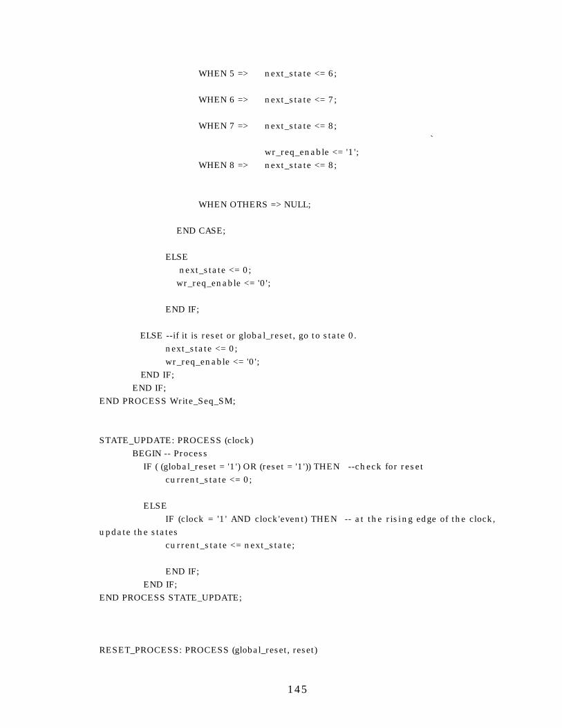
145
WHEN 5 => next_state <= 6; WHEN 6 => next_state <= 7; WHEN 7 => next_state <= 8;
` wr_req_enable <= '1';
WHEN 8 => next_state <= 8; WHEN OTHERS => NULL; END CASE; ELSE next_state <= 0; wr_req_enable <= '0'; END IF; ELSE --if it is reset or global_reset, go to state 0. next_state <= 0; wr_req_enable <= '0'; END IF; END IF; END PROCESS Write_Seq_SM; STATE_UPDATE: PROCESS (clock) BEGIN -- Process IF ( (global_reset = '1') OR (reset = '1')) THEN --check for reset current_state <= 0; ELSE IF (clock = '1' AND clock'event) THEN -- at the rising edge of the clock, update the states current_state <= next_state; END IF; END IF; END PROCESS STATE_UPDATE; RESET_PROCESS: PROCESS (global_reset, reset)
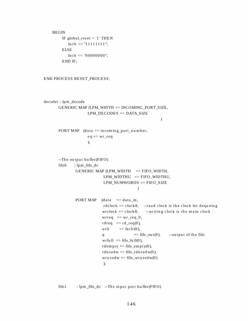
146
BEGIN IF global_reset = '1' THEN faclr <= "11111111"; ELSE faclr <= "00000000"; END IF; END PROCESS RESET_PROCESS; decoder : lpm_decode GENERIC MAP (LPM_WIDTH => INCOMING_PORT_SIZE, LPM_DECODES => DATA_SIZE ) PORT MAP (data => incoming_port_number, eq => wr_req ); --The output buffer(FIFO) fifo0 : lpm_fifo_dc GENERIC MAP (LPM_WIDTH => FIFO_WIDTH, LPM_WIDTHU => FIFO_WIDTHU,
LPM_NUMWORDS => FIFO_SIZE ) PORT MAP (data => data_in, rdclock => clock8, --read clock is the clock for dequeing wrclock => clock8, --writing clock is the main clock
wrreq => wr_req_0, rdreq => rd_req(0), aclr => faclr(0), q => fifo_out(0), --output of the fifo wrfull => fifo_full(0), rdempty => fifo_empty(0), rdusedw => fifo_rdusedw(0), wrusedw => fifo_wrusedw(0) ); fifo1 : lpm_fifo_dc --The input port buffer(FIFO)
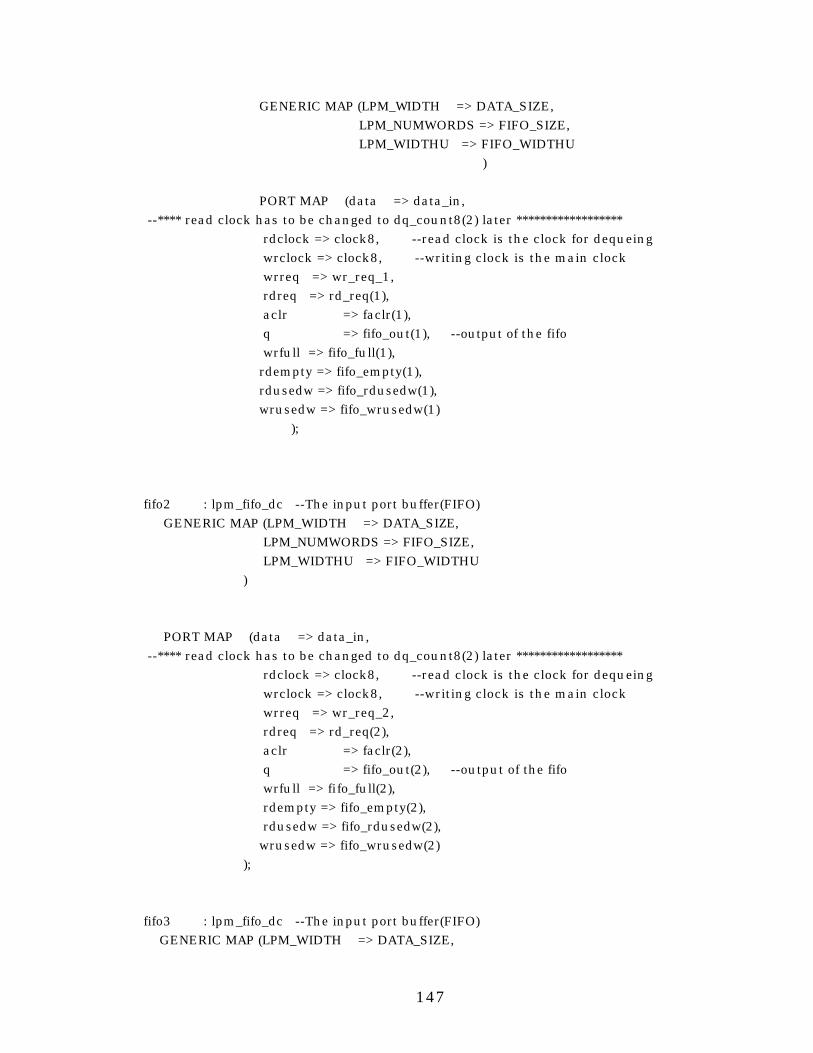
147
GENERIC MAP (LPM_WIDTH => DATA_SIZE, LPM_NUMWORDS => FIFO_SIZE, LPM_WIDTHU => FIFO_WIDTHU ) PORT MAP (data => data_in, --**** read clock has to be changed to dq_count8(2) later ****************** rdclock => clock8, --read clock is the clock for dequeing wrclock => clock8, --writing clock is the main clock
wrreq => wr_req_1, rdreq => rd_req(1),
aclr => faclr(1), q => fifo_out(1), --output of the fifo
wrfull => fifo_full(1), rdempty => fifo_empty(1),
rdusedw => fifo_rdusedw(1), wrusedw => fifo_wrusedw(1) ); fifo2 : lpm_fifo_dc --The input port buffer(FIFO) GENERIC MAP (LPM_WIDTH => DATA_SIZE, LPM_NUMWORDS => FIFO_SIZE, LPM_WIDTHU => FIFO_WIDTHU ) PORT MAP (data => data_in, --**** read clock has to be changed to dq_count8(2) later ****************** rdclock => clock8, --read clock is the clock for dequeing wrclock => clock8, --writing clock is the main clock wrreq => wr_req_2, rdreq => rd_req(2), aclr => faclr(2), q => fifo_out(2), --output of the fifo wrfull => fifo_full(2), rdempty => fifo_empty(2), rdusedw => fifo_rdusedw(2), wrusedw => fifo_wrusedw(2) ); fifo3 : lpm_fifo_dc --The input port buffer(FIFO) GENERIC MAP (LPM_WIDTH => DATA_SIZE,
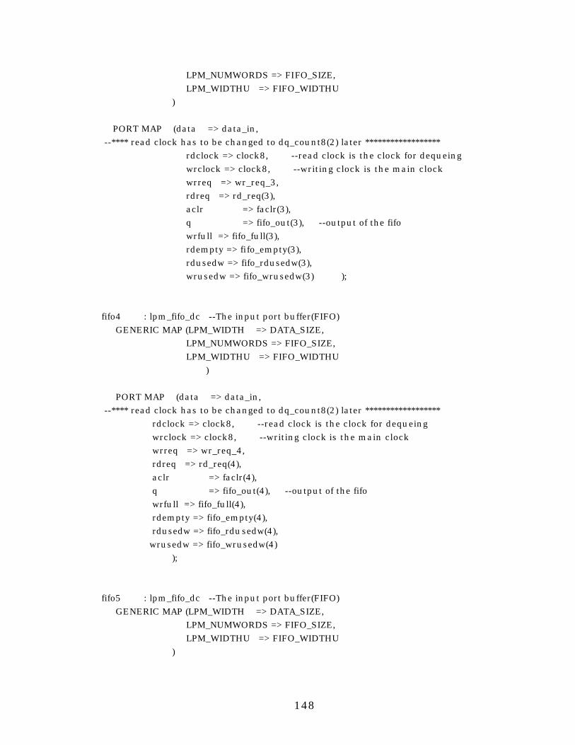
148
LPM_NUMWORDS => FIFO_SIZE, LPM_WIDTHU => FIFO_WIDTHU ) PORT MAP (data => data_in, --**** read clock has to be changed to dq_count8(2) later ****************** rdclock => clock8, --read clock is the clock for dequeing wrclock => clock8, --writing clock is the main clock wrreq => wr_req_3, rdreq => rd_req(3), aclr => faclr(3), q => fifo_out(3), --output of the fifo wrfull => fifo_full(3), rdempty => fifo_empty(3), rdusedw => fifo_rdusedw(3), wrusedw => fifo_wrusedw(3) ); fifo4 : lpm_fifo_dc --The input port buffer(FIFO) GENERIC MAP (LPM_WIDTH => DATA_SIZE, LPM_NUMWORDS => FIFO_SIZE, LPM_WIDTHU => FIFO_WIDTHU ) PORT MAP (data => data_in, --**** read clock has to be changed to dq_count8(2) later ****************** rdclock => clock8, --read clock is the clock for dequeing wrclock => clock8, --writing clock is the main clock wrreq => wr_req_4, rdreq => rd_req(4), aclr => faclr(4), q => fifo_out(4), --output of the fifo wrfull => fifo_full(4), rdempty => fifo_empty(4), rdusedw => fifo_rdusedw(4), wrusedw => fifo_wrusedw(4) ); fifo5 : lpm_fifo_dc --The input port buffer(FIFO) GENERIC MAP (LPM_WIDTH => DATA_SIZE, LPM_NUMWORDS => FIFO_SIZE, LPM_WIDTHU => FIFO_WIDTHU )
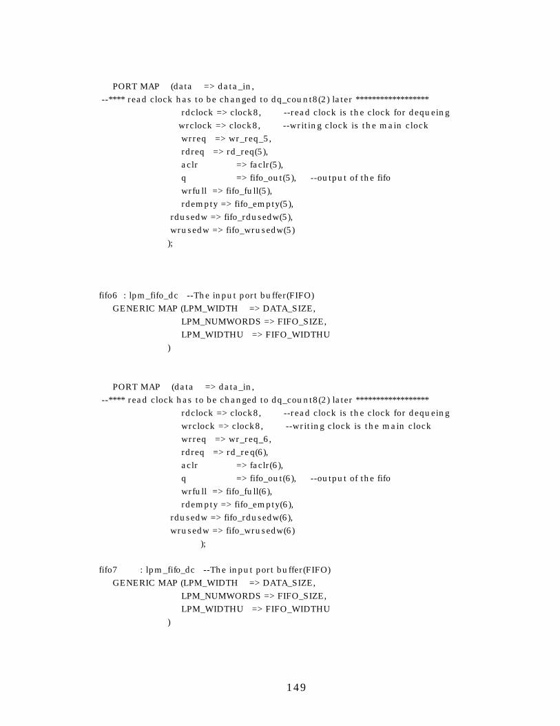
149
PORT MAP (data => data_in, --**** read clock has to be changed to dq_count8(2) later ******************
rdclock => clock8, --read clock is the clock for dequeing wrclock => clock8, --writing clock is the main clock wrreq => wr_req_5, rdreq => rd_req(5), aclr => faclr(5), q => fifo_out(5), --output of the fifo wrfull => fifo_full(5), rdempty => fifo_empty(5), rdusedw => fifo_rdusedw(5), wrusedw => fifo_wrusedw(5) ); fifo6 : lpm_fifo_dc --The input port buffer(FIFO) GENERIC MAP (LPM_WIDTH => DATA_SIZE, LPM_NUMWORDS => FIFO_SIZE, LPM_WIDTHU => FIFO_WIDTHU ) PORT MAP (data => data_in, --**** read clock has to be changed to dq_count8(2) later ****************** rdclock => clock8, --read clock is the clock for dequeing wrclock => clock8, --writing clock is the main clock wrreq => wr_req_6, rdreq => rd_req(6), aclr => faclr(6), q => fifo_out(6), --output of the fifo wrfull => fifo_full(6), rdempty => fifo_empty(6), rdusedw => fifo_rdusedw(6), wrusedw => fifo_wrusedw(6) ); fifo7 : lpm_fifo_dc --The input port buffer(FIFO) GENERIC MAP (LPM_WIDTH => DATA_SIZE, LPM_NUMWORDS => FIFO_SIZE, LPM_WIDTHU => FIFO_WIDTHU )
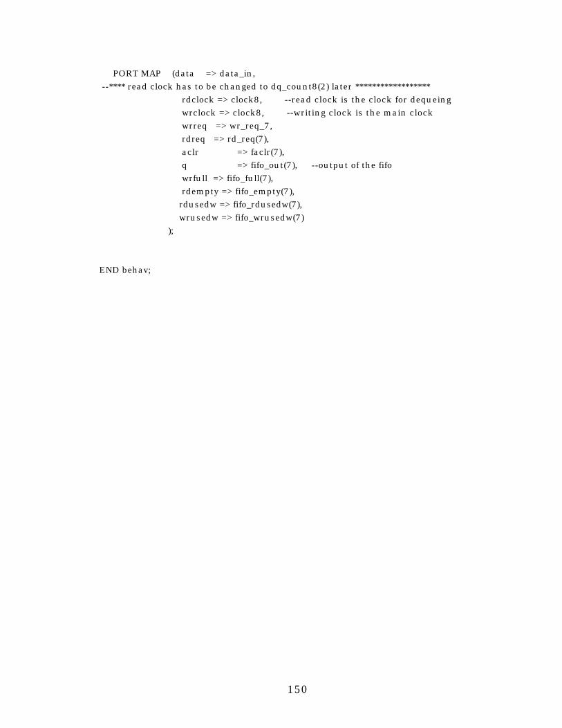
150
PORT MAP (data => data_in, --**** read clock has to be changed to dq_count8(2) later ****************** rdclock => clock8, --read clock is the clock for dequeing wrclock => clock8, --writing clock is the main clock wrreq => wr_req_7, rdreq => rd_req(7), aclr => faclr(7), q => fifo_out(7), --output of the fifo wrfull => fifo_full(7),
rdempty => fifo_empty(7), rdusedw => fifo_rdusedw(7), wrusedw => fifo_wrusedw(7) ); END behav;
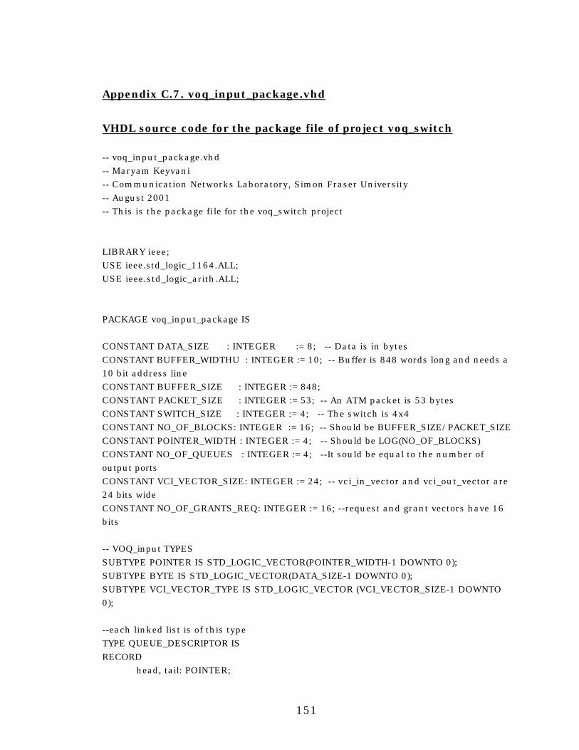
151
Appendix C.7. voq_input_package.vhd
VHDL source code for the package file of project voq_switch -- voq_input_package.vhd -- Maryam Keyvani -- Communication Networks Laboratory, Simon Fraser University -- August 2001 -- This is the package fi le for the voq_switch project LIBRARY ieee; USE ieee.std_logic_1164.ALL; USE ieee.std_logic_arith.ALL; PACKAGE voq_input_package IS CONSTANT DATA_SIZE : INTEGER := 8; -- Data is in bytes CONSTANT BUFFER_WIDTHU : INTEGER := 10; -- Buffer is 848 words long and needs a 10 bit address line CONSTANT BUFFER_SIZE : INTEGER := 848; CONSTANT PACKET_SIZE : INTEGER := 53; -- An ATM packet is 53 bytes CONSTANT SWITCH_SIZE : INTEGER := 4; -- The switch is 4x4 CONSTANT NO_OF_BLOCKS: INTEGER := 16; -- Should be BUFFER_SIZE/PACKET_SIZE CONSTANT POINTER_WIDTH : INTEGER := 4; -- Should be LOG(NO_OF_BLOCKS) CONSTANT NO_OF_QUEUES : INTEGER := 4; --It sould be equal to the number of output ports CONSTANT VCI_VECTOR_SIZE: INTEGER := 24; -- vci_in_vector and vci_out_vector are 24 bits wide CONSTANT NO_OF_GRANTS_REQ: INTEGER := 16; --request and grant vectors have 16 bits -- VOQ_input TYPES SUBTYPE POINTER IS STD_LOGIC_VECTOR(POINTER_WIDTH-1 DOWNTO 0); SUBTYPE BYTE IS STD_LOGIC_VECTOR(DATA_SIZE-1 DOWNTO 0); SUBTYPE VCI_VECTOR_TYPE IS STD_LOGIC_VECTOR (VCI_VECTOR_SIZE-1 DOWNTO 0); --each linked list is of this type TYPE QUEUE_DESCRIPTOR IS RECORD head, tail: POINTER;
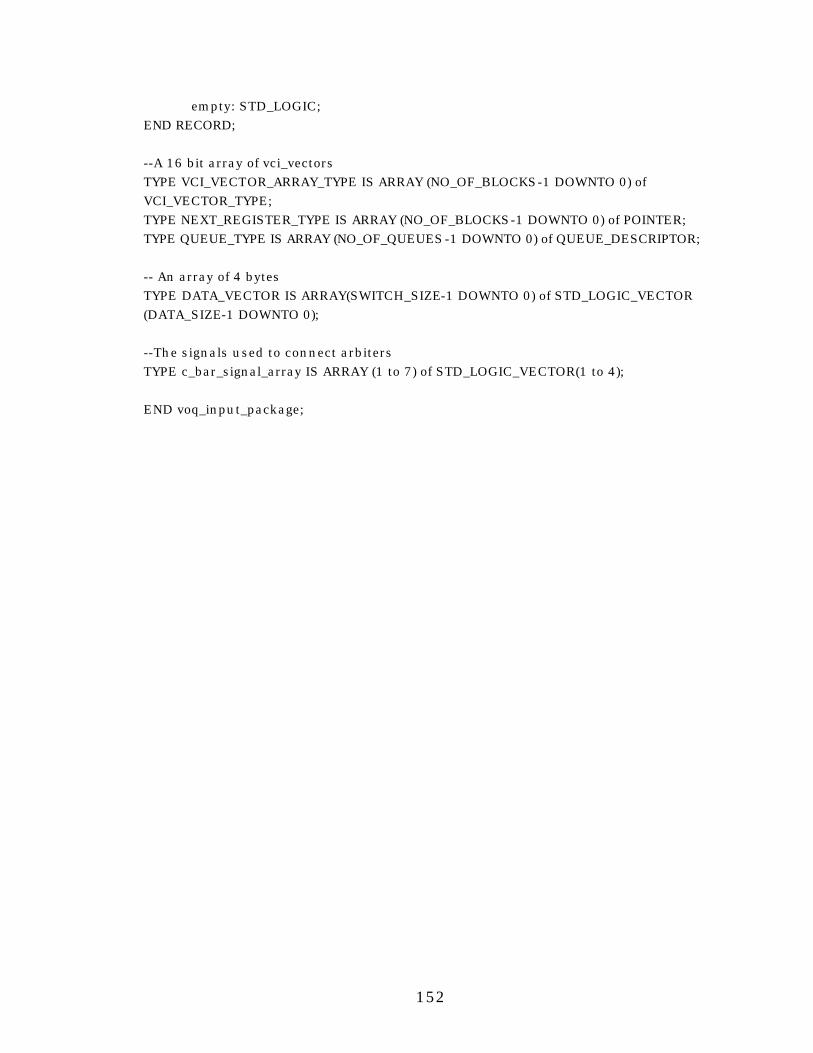
152
empty: STD_LOGIC; END RECORD; --A 16 bit array of vci_vectors TYPE VCI_VECTOR_ARRAY_TYPE IS ARRAY (NO_OF_BLOCKS-1 DOWNTO 0) of VCI_VECTOR_TYPE; TYPE NEXT_REGISTER_TYPE IS ARRAY (NO_OF_BLOCKS-1 DOWNTO 0) of POINTER; TYPE QUEUE_TYPE IS ARRAY (NO_OF_QUEUES-1 DOWNTO 0) of QUEUE_DESCRIPTOR; -- An array of 4 bytes TYPE DATA_VECTOR IS ARRAY(SWITCH_SIZE-1 DOWNTO 0) of STD_LOGIC_VECTOR (DATA_SIZE-1 DOWNTO 0); --The signals used to connect arbiters TYPE c_bar_signal_array IS ARRAY (1 to 7) of STD_LOGIC_VECTOR(1 to 4); END voq_input_package;
153
Appendix D. Simulation results
154
Appendix D.1. Simulation results for the voq_switch project
Pages 143 and 144 contain the simulation results for the voq_switch
project.
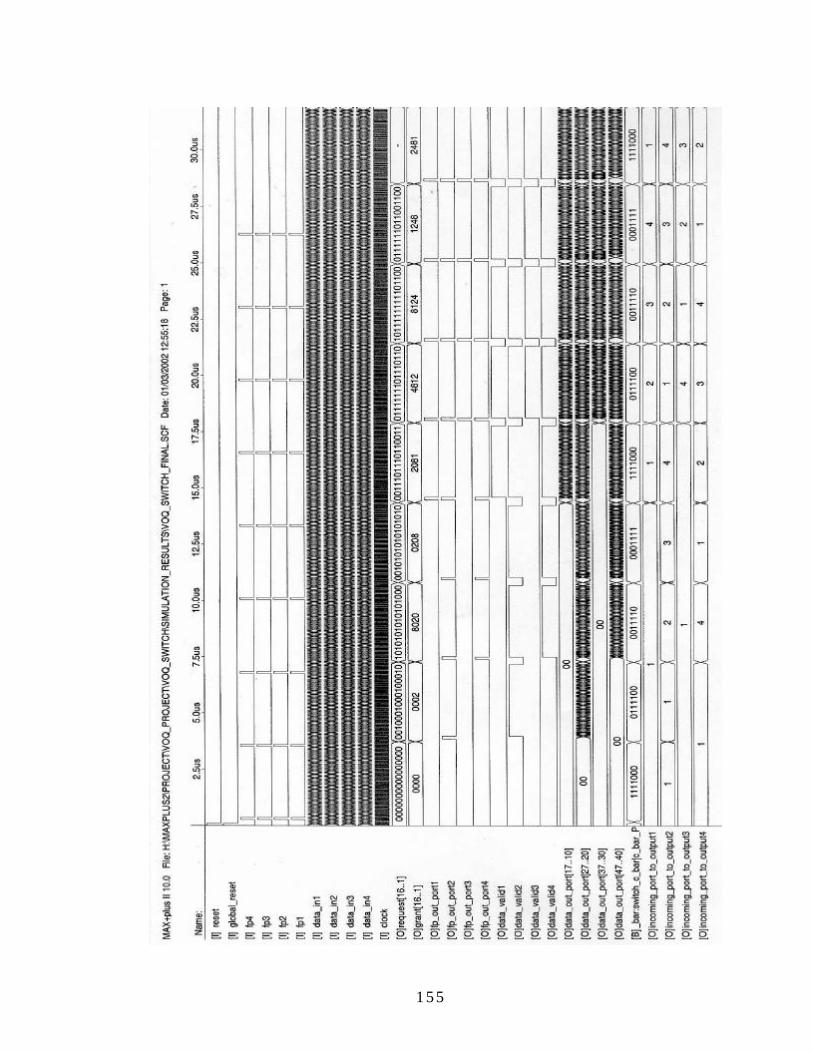
155
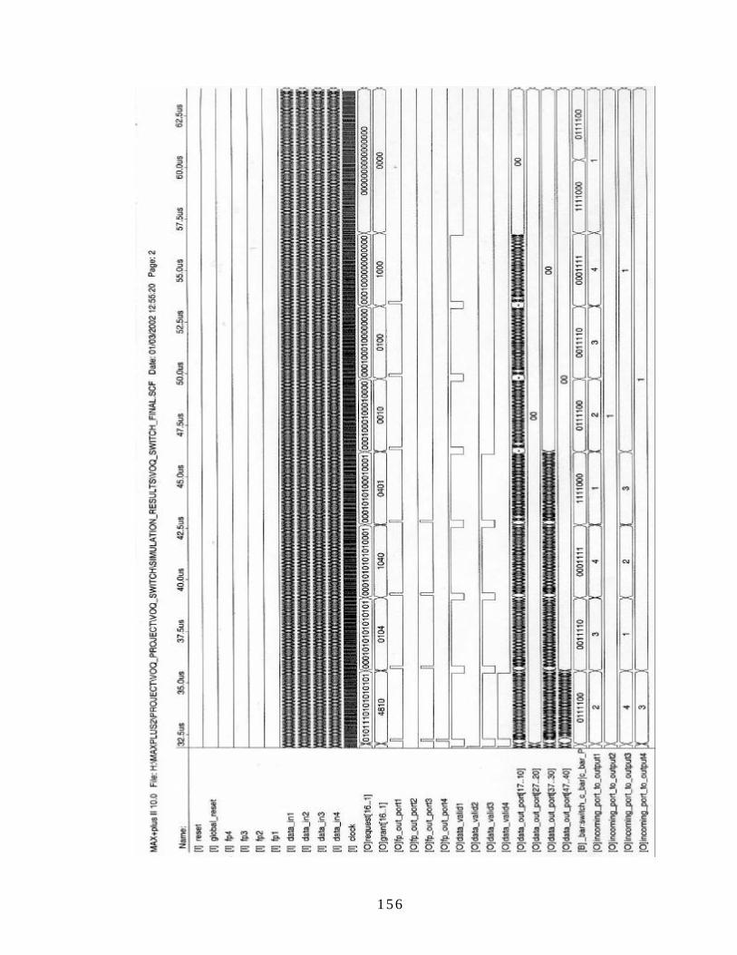
156
157
Appendix D.2. Simulation results for the voq_input project
Pages 146 and 147 contain the simulation results for the voq_input
project.
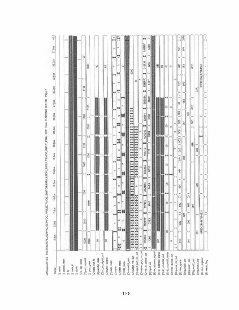
158
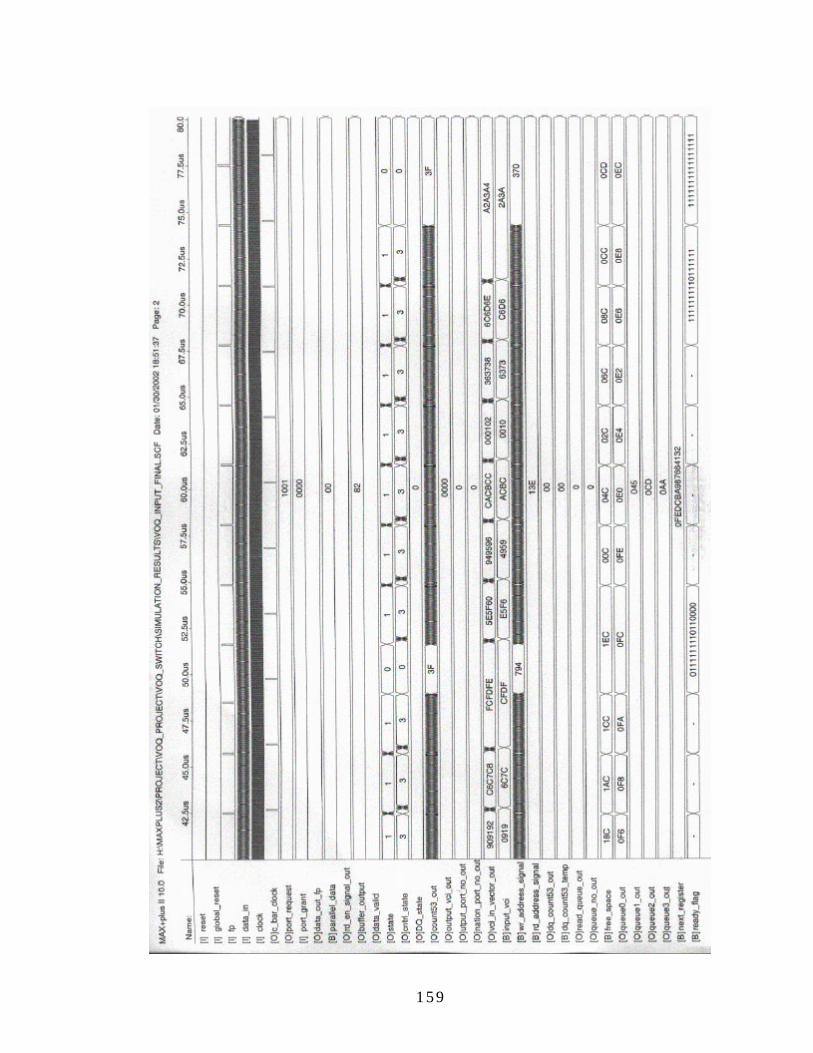
159