Embed Size (px)
Citation preview
VESA DisplayPort Standard MEMBER USE ONLY. DISTRIBUTION TO NON-MEMBERS IS PROHIBITED. Ver.1.2
©Copyright 2007-2010 Video Electronics Standards Association Page 1 of 515
DisplayPort™ Standard
860 Hillview Court, Suite 150 Phone: 408 957 9270 Milpitas, CA 95035 Fax: 408 957 9277 URL: www.vesa.org
VESA DisplayPort Standard
Version 1, Revision 2
January 5, 2010
Purpose The purpose of this document is to define a flexible system and apparatus capable of transporting video, audio and other data between a Source Device and a Sink Device over a digital communications interface.
Summary The DisplayPort™ standard specifies an open digital communications interface for use in both internal connections, such as interfaces within a PC or monitor, and external display connections. Suitable external display connections include interfaces between a PC and monitor or projector, between a PC and TV, or between a device such as a DVD player and TV display.
DisplayPort Ver.1.1a is revised to correct errata items in and add clarifications to DisplayPort Standard Version 1, Revision 1.
DisplayPort Ver. 1.2 is revised to add enhancements including higher speed operation, more flexible topology management, multiple streams on a single connection, higher speed Auxiliary Channel communications, improved support for audio, and a new smaller connector. It also corrects errata items in and adds clarifications to DisplayPort Standard Version 1, Revision 1a.
VESA DisplayPort Standard MEMBER USE ONLY. DISTRIBUTION TO NON-MEMBERS IS PROHIBITED. Ver.1.2
©Copyright 2007-2010 Video Electronics Standards Association Page 2 of 515
Table of Contents Preface ...............................................................................................................................................................15 Acknowledgements............................................................................................................................................17 Revision History ................................................................................................................................................20 1 Introduction .................................................................................................................................................21
1.1 DisplayPort Standard Organization ......................................................................................................21 1.2 DisplayPort Objectives .........................................................................................................................21
1.2.1 Key Industry Needs for DisplayPort ..............................................................................................................22 1.2.2 DisplayPort Technical Objectives..................................................................................................................22 1.2.3 DisplayPort External Connection Objectives.................................................................................................23 1.2.4 DisplayPort Internal Connection Objectives..................................................................................................24 1.2.5 DisplayPort CE Connection Objectives .........................................................................................................24 1.2.6 Content Protection for DisplayPort................................................................................................................24
1.3 Acronyms..............................................................................................................................................24 1.4 Glossary ................................................................................................................................................27 1.5 Reference Documents ...........................................................................................................................31 1.6 Nomenclature for Bit and Byte Ordering..............................................................................................32
1.6.1 Bit Ordering ...................................................................................................................................................32 1.6.2 Byte Ordering ................................................................................................................................................33
1.7 Overview of DisplayPort ......................................................................................................................34 1.7.1 Make-up of the Main Link .............................................................................................................................34 1.7.2 Make-up of AUX CH.....................................................................................................................................35 1.7.3 Link Configuration and Management ............................................................................................................35 1.7.4 Layered, Modular Architecture......................................................................................................................36
2 Link Layer ...................................................................................................................................................37 2.1 SST Mode Introduction.........................................................................................................................37
2.1.1 Number of Lanes and Per-lane Data Rate (Applicable both in SST and MST Modes) .................................38 2.1.2 Number of Main, Uncompressed Video Streams in SST Mode ....................................................................38 2.1.3 Basic Functions (Applicable both in SST and MST Modes) .........................................................................38 2.1.4 DisplayPort Device Types and Link Topology in SST Mode........................................................................38
2.2 Isochronous Transport Services in SST Mode......................................................................................43 2.2.1 Main Stream to Main Link Lane Mapping in the Source Device ..................................................................43 2.2.2 Stream Reconstruction in the Sink.................................................................................................................71 2.2.3 Stream Clock Recovery .................................................................................................................................72 2.2.4 Main Stream Attribute Data Transport ..........................................................................................................74 2.2.5 Secondary-data Packing Formats...................................................................................................................79 2.2.6 ECC for Secondary-data Packet...................................................................................................................101
2.3 AUX CH States and Arbitration .........................................................................................................107 2.3.1 AUX CH STATES Overview ......................................................................................................................107 2.3.2 Link Layer Arbitration Control....................................................................................................................111 2.3.3 Policy Maker AUX CH Management ..........................................................................................................111 2.3.4 Detailed uPacket TX AUX CH State Description .......................................................................................112 2.3.5 Detailed uPacket RX AUX CH State Description .......................................................................................113
2.4 Overview of DP Multi-Stream Transport (MST) Isochronous Transport Service..............................114 2.4.1 Connection-oriented Transport ....................................................................................................................115 2.4.2 Layers of DP Isochronous Transport Service ..............................................................................................117 2.4.3 Sideband CH Communications....................................................................................................................121
2.5 Topology Management Layer.............................................................................................................122 2.5.1 Primitives of MST DP Devices and Device Types ......................................................................................122 2.5.2 MST Topologies ..........................................................................................................................................125 2.5.3 MST Device Identification...........................................................................................................................126 2.5.4 Topology Manager and Topology Assistant ................................................................................................127
VESA DisplayPort Standard MEMBER USE ONLY. DISTRIBUTION TO NON-MEMBERS IS PROHIBITED. Ver.1.2
©Copyright 2007-2010 Video Electronics Standards Association Page 3 of 515
2.5.5 Topology Discovery.....................................................................................................................................128 2.5.6 Topology Maintenance ................................................................................................................................128 2.5.7 Topologies with SST-only Source devices ..................................................................................................129 2.5.8 Loop Handling .............................................................................................................................................129
2.6 Multi-Stream Transport Operation......................................................................................................131 2.6.1 Link Timing Generation Based on Multi-Stream Transport Packet ............................................................135 2.6.2 Symbol Sequence Mapping into VC Payload ..............................................................................................136 2.6.3 Time Slot Count Allocation to VC Payload.................................................................................................144 2.6.4 VC Payload Allocation Synchronization Management................................................................................150 2.6.5 ALLOCATE_PAYLOAD Timing Sequence...............................................................................................154 2.6.6 Impacts of Various Events on VC Payload ID Table...................................................................................161 2.6.7 Robustness Requirement..............................................................................................................................164 2.6.8 Control Functions, Control Symbols and K-Code Assignment ...................................................................164 2.6.9 Conversion Between MST and SST Symbol Mapping................................................................................166 2.6.10 MTPH Usages for CP Extension in MST Mode .........................................................................................167
2.7 AUX Transaction Syntax in Manchester Transaction Format ............................................................170 2.7.1 Command definition ....................................................................................................................................171 2.7.2 AUX Transaction Response/Reply Time-outs.............................................................................................173 2.7.3 Native AUX Request Transaction Syntax....................................................................................................173 2.7.4 Native AUX Reply Transaction Syntax.......................................................................................................174 2.7.5 I2C Bus Transaction Mapping onto AUX Syntax ........................................................................................174 2.7.6 Conversion of I2C Transaction to Native AUX Transaction (Informative) .................................................192 2.7.7 I2C-overAUX Transaction Clarifications and Implementation Rules..........................................................192
2.8 Transaction Syntax in FAUX Transaction Format .............................................................................202 2.9 AUX CH Services...............................................................................................................................203
2.9.1 Stream Transport Initiation Sequence..........................................................................................................203 2.9.2 Stream Transport Termination Sequence.....................................................................................................204 2.9.3 AUX Link Services......................................................................................................................................205 2.9.4 AUX Device Services ..................................................................................................................................253
2.10 Protocol Differentiation for Embedded DisplayPort (eDP) ................................................................255 2.10.1 Overview.....................................................................................................................................................255 2.10.2 Protocol Differentiation Methods................................................................................................................255 2.10.3 eDP Source Behavior (Informative)............................................................................................................255 2.10.4 Symbol Error Rate Measurement Pattern Output (Informative) .................................................................256
2.11 Messaging AUX Client.......................................................................................................................258 2.11.1 Messaging AUX Client Layers ...................................................................................................................259 2.11.2 Message Transaction Layer.........................................................................................................................260 2.11.3 Sideband MSG Layer ..................................................................................................................................268 2.11.4 AUX CH Support for Messaging AUX Client............................................................................................273 2.11.5 RAD (Relative Address) Updated by MST Devices in the Path .................................................................274 2.11.6 Broadcast Message Transactions ................................................................................................................275 2.11.7 Message Delivery........................................................................................................................................276 2.11.8 Error Handling ............................................................................................................................................279 2.11.9 Descriptions of Available Message Transaction Requests..........................................................................281
2.12 Audio-to-Video & Audio-to-Audio Synchronization .........................................................................297 2.12.1 Overview.....................................................................................................................................................297 2.12.2 DisplayPort AV Sync Data Block (AVSDB)..............................................................................................298 2.12.3 Delay Compensation ...................................................................................................................................298
2.13 Global Time Code and Audio Inter-channel Sync..............................................................................304 2.13.1 Global Time Code.......................................................................................................................................304 2.13.2 Application of GTC for Audio Inter-channel Synchronization...................................................................307
3 Physical Layer ...........................................................................................................................................309 3.1 Introduction.........................................................................................................................................309
3.1.1 PHY Functions.............................................................................................................................................309 3.1.2 Link Layer-PHY Interface Signals...............................................................................................................310 3.1.3 PHY-Media Interface Signals ......................................................................................................................311
VESA DisplayPort Standard MEMBER USE ONLY. DISTRIBUTION TO NON-MEMBERS IS PROHIBITED. Ver.1.2
©Copyright 2007-2010 Video Electronics Standards Association Page 4 of 515
3.1.4 Compliance Measurement Points.................................................................................................................312 3.1.5 Electrical Signal Definitions ........................................................................................................................319 3.1.6 Scrambling ...................................................................................................................................................323 3.1.7 Symbol Coding and Serialization/De-serialization ......................................................................................324
3.2 DP_PWR for Box-to-Box DisplayPort Connection............................................................................325 3.2.1 DP_PWR User Detection Method ...............................................................................................................326 3.2.2 DP_PWR Wire.............................................................................................................................................326 3.2.3 Inrush Energy...............................................................................................................................................326 3.2.4 Voltage Droop..............................................................................................................................................326 3.2.5 Over-Current Protection...............................................................................................................................326
3.3 Hot Plug/Unplug Detect Circuitry ......................................................................................................327 3.4 AUX Channel......................................................................................................................................329
3.4.1 AUX Channel Logical Sub-block ................................................................................................................329 3.4.2 AUX Channel Electrical Sub-block .............................................................................................................341
3.5 Main Link............................................................................................................................................353 3.5.1 Main Link Logic Sub-block.........................................................................................................................353 3.5.2 Main Link Electrical Sub-Block ..................................................................................................................362 3.5.3 Transmitter and Receiver Electrical Parameters ..........................................................................................362 3.5.4 ESD and EOS Protection .............................................................................................................................378
4 Mechanical ................................................................................................................................................379 4.1 Cable-Connector Assembly Specifications (for box-to-box)..............................................................379
4.1.1 Cable-Connector Assembly Definition ........................................................................................................380 4.1.2 Type of Bulk Cable......................................................................................................................................383 4.1.3 Impedance Profile ........................................................................................................................................384 4.1.4 Insertion Loss & Return Loss ......................................................................................................................386 4.1.5 High Bit Rate Cable-Connector Assembly Specification ............................................................................387 4.1.6 Reduced Bit Rate Cable-Connector Assembly Specification ......................................................................397
4.2 Connector Specification......................................................................................................................401 4.2.1 External full-size connector .........................................................................................................................401 4.2.2 Mini DisplayPort External Connector..........................................................................................................413 4.2.3 Panel-side Internal Connector (Informative)................................................................................................438
5 Source/Sink/Branch Device Policy Requirements for Interoperability .....................................................446 5.1 Source Device in SST Mode...............................................................................................................446
5.1.1 Stream Source Requirement.........................................................................................................................446 5.1.2 Source Device Link Configuration Requirement.........................................................................................449 5.1.3 Source Device Behavior on Stream Timing Change....................................................................................449 5.1.4 Source Device Behavior upon HPD Pulse Detection...................................................................................450 5.1.5 Downstream Device uPacket RX Power Management by a Source Device ................................................452 5.1.6 Source Device Connected to a Branch Device.............................................................................................452
5.2 Sink Device in SST Mode...................................................................................................................452 5.2.1 Stream Sink Requirement ............................................................................................................................452 5.2.2 Sink Device Link Configuration Requirement.............................................................................................453 5.2.3 Sink Device Behavior on Stream Timing Change .......................................................................................454 5.2.4 Toggling of HPD Signal for Status Change Notification.............................................................................454 5.2.5 Sink Device uPacket RX Power-Save Mode ...............................................................................................454
5.3 Branch Device in SST-only Mode ......................................................................................................458 5.3.1 EDID Access Handling Requirement ..........................................................................................................458 5.3.2 Branch Device Link Configuration Requirements.......................................................................................458
5.4 Source Device in MST Mode..............................................................................................................462 5.5 Sink Device in MST Mode .................................................................................................................463 5.6 Branch Device in MST Mode .............................................................................................................463 5.7 Cable-Connector Assembly ................................................................................................................463
5.7.1 Box-to-Box, End-User-Detachable Cable Assembly...................................................................................463 5.7.2 Embedded and Captive Cable Assembly .....................................................................................................464
VESA DisplayPort Standard MEMBER USE ONLY. DISTRIBUTION TO NON-MEMBERS IS PROHIBITED. Ver.1.2
©Copyright 2007-2010 Video Electronics Standards Association Page 5 of 515
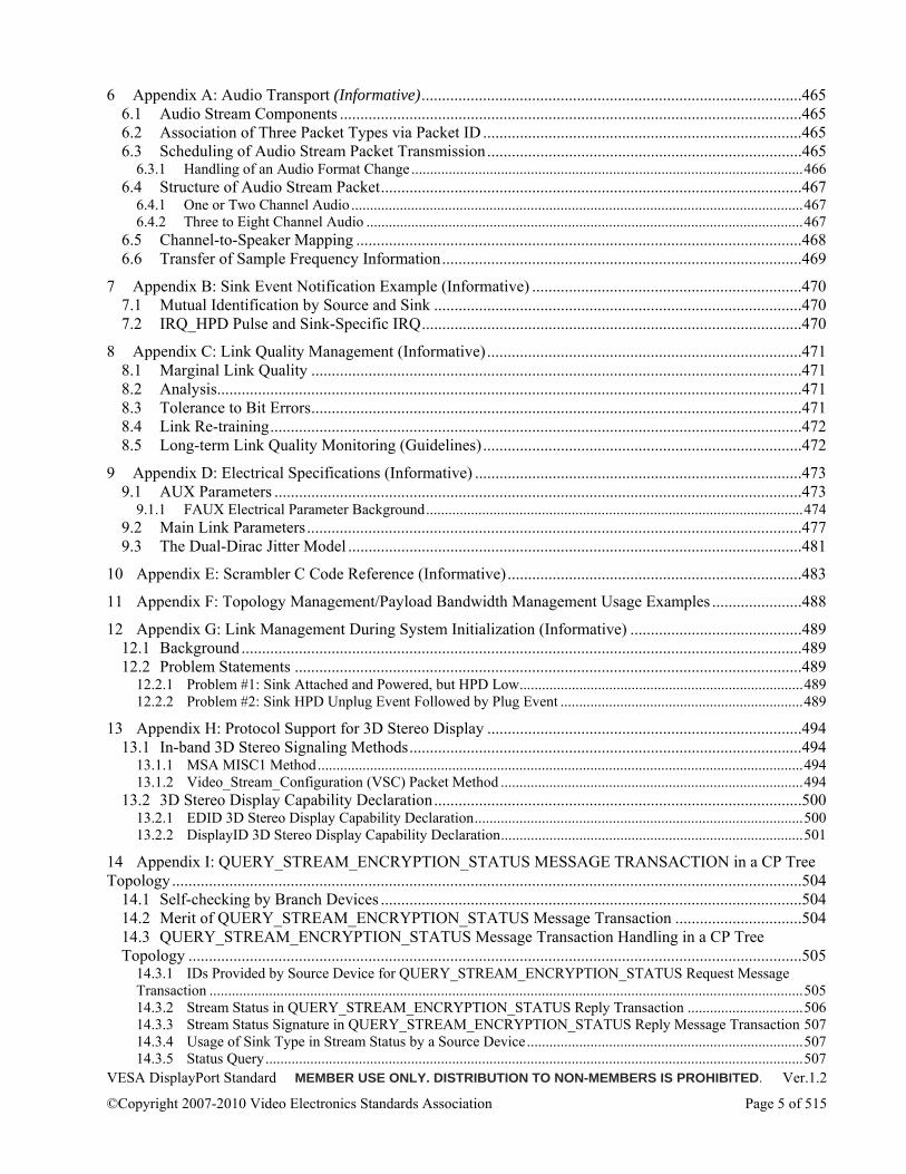
6 Appendix A: Audio Transport (Informative).............................................................................................465 6.1 Audio Stream Components .................................................................................................................465 6.2 Association of Three Packet Types via Packet ID ..............................................................................465 6.3 Scheduling of Audio Stream Packet Transmission.............................................................................465
6.3.1 Handling of an Audio Format Change .........................................................................................................466 6.4 Structure of Audio Stream Packet.......................................................................................................467
6.4.1 One or Two Channel Audio .........................................................................................................................467 6.4.2 Three to Eight Channel Audio .....................................................................................................................467
6.5 Channel-to-Speaker Mapping .............................................................................................................468 6.6 Transfer of Sample Frequency Information........................................................................................469
7 Appendix B: Sink Event Notification Example (Informative) ..................................................................470 7.1 Mutual Identification by Source and Sink ..........................................................................................470 7.2 IRQ_HPD Pulse and Sink-Specific IRQ.............................................................................................470
8 Appendix C: Link Quality Management (Informative).............................................................................471 8.1 Marginal Link Quality ........................................................................................................................471 8.2 Analysis...............................................................................................................................................471 8.3 Tolerance to Bit Errors........................................................................................................................471 8.4 Link Re-training..................................................................................................................................472 8.5 Long-term Link Quality Monitoring (Guidelines) ..............................................................................472
9 Appendix D: Electrical Specifications (Informative) ................................................................................473 9.1 AUX Parameters .................................................................................................................................473
9.1.1 FAUX Electrical Parameter Background.....................................................................................................474 9.2 Main Link Parameters.........................................................................................................................477 9.3 The Dual-Dirac Jitter Model ...............................................................................................................481
10 Appendix E: Scrambler C Code Reference (Informative)........................................................................483 11 Appendix F: Topology Management/Payload Bandwidth Management Usage Examples ......................488 12 Appendix G: Link Management During System Initialization (Informative) ..........................................489
12.1 Background .........................................................................................................................................489 12.2 Problem Statements ............................................................................................................................489
12.2.1 Problem #1: Sink Attached and Powered, but HPD Low............................................................................489 12.2.2 Problem #2: Sink HPD Unplug Event Followed by Plug Event .................................................................489
13 Appendix H: Protocol Support for 3D Stereo Display .............................................................................494 13.1 In-band 3D Stereo Signaling Methods................................................................................................494
13.1.1 MSA MISC1 Method..................................................................................................................................494 13.1.2 Video_Stream_Configuration (VSC) Packet Method .................................................................................494
13.2 3D Stereo Display Capability Declaration..........................................................................................500 13.2.1 EDID 3D Stereo Display Capability Declaration........................................................................................500 13.2.2 DisplayID 3D Stereo Display Capability Declaration.................................................................................501
14 Appendix I: QUERY_STREAM_ENCRYPTION_STATUS MESSAGE TRANSACTION in a CP Tree Topology..........................................................................................................................................................504
14.1 Self-checking by Branch Devices .......................................................................................................504 14.2 Merit of QUERY_STREAM_ENCRYPTION_STATUS Message Transaction ...............................504 14.3 QUERY_STREAM_ENCRYPTION_STATUS Message Transaction Handling in a CP Tree Topology ......................................................................................................................................................505
14.3.1 IDs Provided by Source Device for QUERY_STREAM_ENCRYPTION_STATUS Request Message Transaction ...............................................................................................................................................................505 14.3.2 Stream Status in QUERY_STREAM_ENCRYPTION_STATUS Reply Transaction ...............................506 14.3.3 Stream Status Signature in QUERY_STREAM_ENCRYPTION_STATUS Reply Message Transaction 507 14.3.4 Usage of Sink Type in Stream Status by a Source Device..........................................................................507 14.3.5 Status Query................................................................................................................................................507
VESA DisplayPort Standard MEMBER USE ONLY. DISTRIBUTION TO NON-MEMBERS IS PROHIBITED. Ver.1.2
©Copyright 2007-2010 Video Electronics Standards Association Page 6 of 515
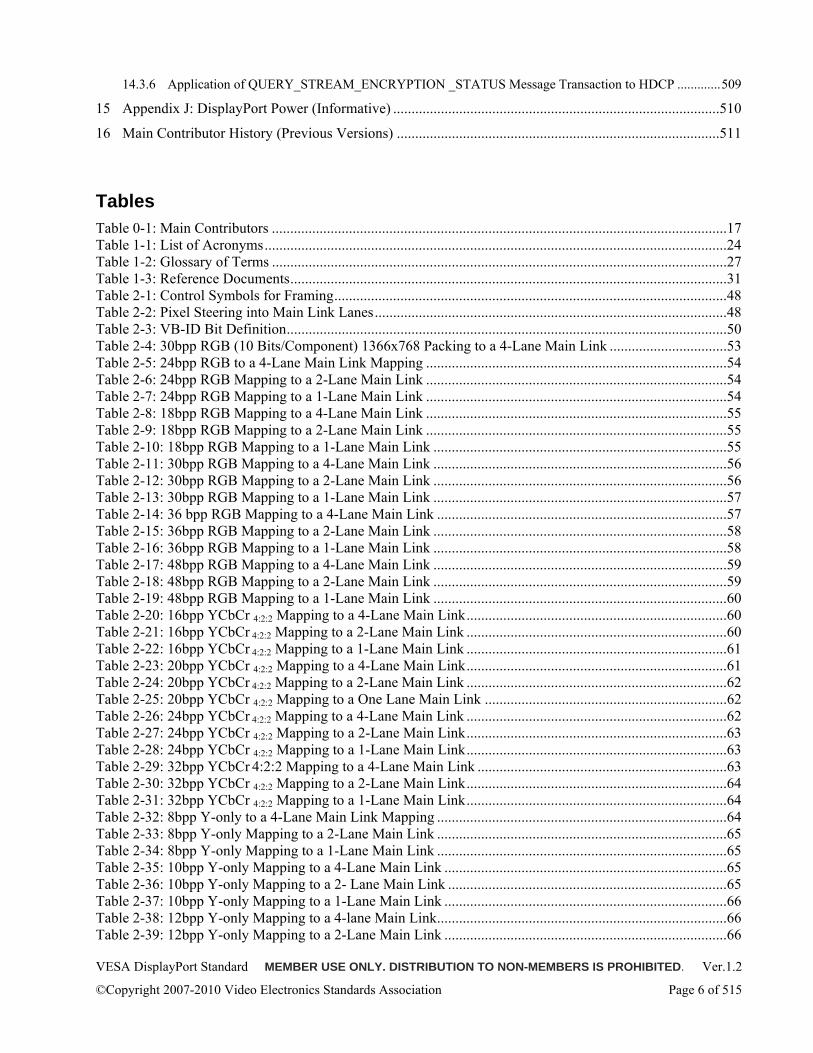
14.3.6 Application of QUERY_STREAM_ENCRYPTION _STATUS Message Transaction to HDCP .............509 15 Appendix J: DisplayPort Power (Informative) .........................................................................................510 16 Main Contributor History (Previous Versions) ........................................................................................511
Tables Table 0-1: Main Contributors ............................................................................................................................17 Table 1-1: List of Acronyms..............................................................................................................................24 Table 1-2: Glossary of Terms ............................................................................................................................27 Table 1-3: Reference Documents.......................................................................................................................31 Table 2-1: Control Symbols for Framing...........................................................................................................48 Table 2-2: Pixel Steering into Main Link Lanes................................................................................................48 Table 2-3: VB-ID Bit Definition........................................................................................................................50 Table 2-4: 30bpp RGB (10 Bits/Component) 1366x768 Packing to a 4-Lane Main Link ................................53 Table 2-5: 24bpp RGB to a 4-Lane Main Link Mapping ..................................................................................54 Table 2-6: 24bpp RGB Mapping to a 2-Lane Main Link ..................................................................................54 Table 2-7: 24bpp RGB Mapping to a 1-Lane Main Link ..................................................................................54 Table 2-8: 18bpp RGB Mapping to a 4-Lane Main Link ..................................................................................55 Table 2-9: 18bpp RGB Mapping to a 2-Lane Main Link ..................................................................................55 Table 2-10: 18bpp RGB Mapping to a 1-Lane Main Link ................................................................................55 Table 2-11: 30bpp RGB Mapping to a 4-Lane Main Link ................................................................................56 Table 2-12: 30bpp RGB Mapping to a 2-Lane Main Link ................................................................................56 Table 2-13: 30bpp RGB Mapping to a 1-Lane Main Link ................................................................................57 Table 2-14: 36 bpp RGB Mapping to a 4-Lane Main Link ...............................................................................57 Table 2-15: 36bpp RGB Mapping to a 2-Lane Main Link ................................................................................58 Table 2-16: 36bpp RGB Mapping to a 1-Lane Main Link ................................................................................58 Table 2-17: 48bpp RGB Mapping to a 4-Lane Main Link ................................................................................59 Table 2-18: 48bpp RGB Mapping to a 2-Lane Main Link ................................................................................59 Table 2-19: 48bpp RGB Mapping to a 1-Lane Main Link ................................................................................60 Table 2-20: 16bpp YCbCr 4:2:2 Mapping to a 4-Lane Main Link.......................................................................60 Table 2-21: 16bpp YCbCr 4:2:2 Mapping to a 2-Lane Main Link .......................................................................60 Table 2-22: 16bpp YCbCr 4:2:2 Mapping to a 1-Lane Main Link .......................................................................61 Table 2-23: 20bpp YCbCr 4:2:2 Mapping to a 4-Lane Main Link.......................................................................61 Table 2-24: 20bpp YCbCr 4:2:2 Mapping to a 2-Lane Main Link .......................................................................62 Table 2-25: 20bpp YCbCr 4:2:2 Mapping to a One Lane Main Link ..................................................................62 Table 2-26: 24bpp YCbCr 4:2:2 Mapping to a 4-Lane Main Link .......................................................................62 Table 2-27: 24bpp YCbCr 4:2:2 Mapping to a 2-Lane Main Link.......................................................................63 Table 2-28: 24bpp YCbCr 4:2:2 Mapping to a 1-Lane Main Link.......................................................................63 Table 2-29: 32bpp YCbCr 4:2:2 Mapping to a 4-Lane Main Link ....................................................................63 Table 2-30: 32bpp YCbCr 4:2:2 Mapping to a 2-Lane Main Link.......................................................................64 Table 2-31: 32bpp YCbCr 4:2:2 Mapping to a 1-Lane Main Link.......................................................................64 Table 2-32: 8bpp Y-only to a 4-Lane Main Link Mapping ...............................................................................64 Table 2-33: 8bpp Y-only Mapping to a 2-Lane Main Link ...............................................................................65 Table 2-34: 8bpp Y-only Mapping to a 1-Lane Main Link ...............................................................................65 Table 2-35: 10bpp Y-only Mapping to a 4-Lane Main Link .............................................................................65 Table 2-36: 10bpp Y-only Mapping to a 2- Lane Main Link ............................................................................65 Table 2-37: 10bpp Y-only Mapping to a 1-Lane Main Link .............................................................................66 Table 2-38: 12bpp Y-only Mapping to a 4-lane Main Link...............................................................................66 Table 2-39: 12bpp Y-only Mapping to a 2-Lane Main Link .............................................................................66
VESA DisplayPort Standard MEMBER USE ONLY. DISTRIBUTION TO NON-MEMBERS IS PROHIBITED. Ver.1.2
©Copyright 2007-2010 Video Electronics Standards Association Page 7 of 515
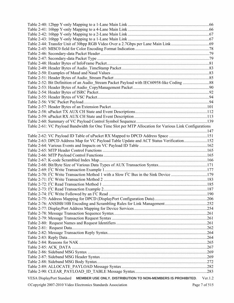
Table 2-40: 12bpp Y-only Mapping to a 1-Lane Main Link .............................................................................66 Table 2-41: 16bpp Y-only Mapping to a 4-Lane Main Link .............................................................................66 Table 2-42: 16bpp Y-only Mapping to a 2-Lane Main Link .............................................................................67 Table 2-43: 16bpp Y-only Mapping to a 1-Lane Main Link .............................................................................67 Table 2-44: Transfer Unit of 30bpp RGB Video Over a 2.7Gbps per Lane Main Link ....................................69 Table 2-45: MISC0 field for Color Encoding Format Indication ......................................................................78 Table 2-46: Secondary-data Packet Header .......................................................................................................79 Table 2-47: Secondary-data Packet Type ..........................................................................................................79 Table 2-48: Header Bytes of InfoFrame Packet.................................................................................................81 Table 2-49: Header Bytes of Audio_TimeStamp Packet ...................................................................................83 Table 2-50: Examples of Maud and Naud Values .............................................................................................83 Table 2-51: Header Bytes of Audio_Stream Packet ..........................................................................................85 Table 2-52: Bit Definition of an Audio_Stream Packet Payload with IEC60958-like Coding .........................88 Table 2-53: Header Bytes of Audio_CopyManagement Packet ........................................................................90 Table 2-54: Header Bytes of ISRC Packet.........................................................................................................92 Table 2-55: Header Bytes of VSC Packet..........................................................................................................94 Table 2-56: VSC Packet Payload.......................................................................................................................94 Table 2-57: Header Bytes of an Extension Packet...........................................................................................101 Table 2-58: uPacket TX AUX CH State and Event Descriptions....................................................................112 Table 2-59: uPacket RX AUX CH State and Event Description .....................................................................113 Table 2-60: Summary of VC Payload Control Symbol Sequence ...................................................................139 Table 2-61: VC Payload Bandwidth for One Time Slot per MTP Allocation for Various Link Configurations
.................................................................................................................................................................147 Table 2-62: VC Payload ID Table of uPacket RX Mapped to DPCD Address Space ....................................151 Table 2-63: DPCD Address Map for VC Payload Table Update and ACT Status Verification......................152 Table 2-64: Various Events and Impacts on VC Payload ID Table ................................................................162 Table 2-65: MTP Header Control Functions ...................................................................................................165 Table 2-66: MTP Payload Control Functions ..................................................................................................165 Table 2-67: K-code Scrambled Index Map......................................................................................................166 Table 2-68: Bit/Byte Size of Various Data Types of AUX Transaction Syntax..............................................171 Table 2-69: I2C Write Transaction Example 1.................................................................................................177 Table 2-70: I2C Write Transaction Method 1 with a Slow I2C Bus in the Sink Device ..................................179 Table 2-71: I2C Write Transaction Method 2 ..................................................................................................183 Table 2-72: I2C Read Transaction Method 1 ...................................................................................................185 Table 2-73: I2C Read Transaction Example 2..................................................................................................187 Table 2-74: I2C Write Followed by an I2C Read .............................................................................................190 Table 2-75: Address Mapping for DPCD (DisplayPort Configuration Data)..................................................206 Table 2-76: ANSI8B/10B Encoding and Scrambling Rules for Link Management........................................252 Table 2-77: DisplayPort Address Mapping for Device Services .....................................................................254 Table 2-78: Message Transaction Sequence Syntax........................................................................................261 Table 2-79: Message Transaction Request Syntax ..........................................................................................261 Table 2-80: Request Names and Request Identifiers ......................................................................................261 Table 2-81: Request Data................................................................................................................................262 Table 2-82: Message Transaction Reply Syntax..............................................................................................264 Table 2-83: Reply Data ....................................................................................................................................264 Table 2-84: Reasons for NAK .........................................................................................................................265 Table 2-85: ACK_DATA ................................................................................................................................267 Table 2-86: Sideband MSG Syntax .................................................................................................................269 Table 2-87: Sideband MSG Header Syntax.....................................................................................................269 Table 2-88: Sideband MSG Body Syntax........................................................................................................272 Table 2-89: ALLOCATE_PAYLOAD Message Syntax.................................................................................282 Table 2-90: CLEAR_PAYLOAD_ID_TABLE Message Syntax....................................................................283
VESA DisplayPort Standard MEMBER USE ONLY. DISTRIBUTION TO NON-MEMBERS IS PROHIBITED. Ver.1.2
©Copyright 2007-2010 Video Electronics Standards Association Page 8 of 515
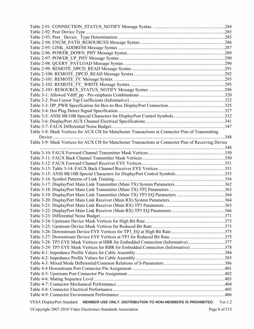
Table 2-91: CONNECTION_STATUS_NOTIFY Message Syntax ...............................................................284 Table 2-92: Peer Device Type .........................................................................................................................285 Table 2-93: Peer_ Device_ Type Determination .............................................................................................285 Table 2-94: ENUM_PATH_RESOURCES Message Syntax..........................................................................286 Table 2-95: LINK_ADDRESS Message Syntax .............................................................................................287 Table 2-96: POWER_DOWN_PHY Message Syntax.....................................................................................289 Table 2-97: POWER_UP_PHY Message Syntax ............................................................................................290 Table 2-98: QUERY_PAYLOAD Message Syntax ........................................................................................290 Table 2-99: REMOTE_DPCD_READ Message Syntax .................................................................................291 Table 2-100: REMOTE_DPCD_READ Message Syntax ...............................................................................292 Table 2-101: REMOTE_I2C Message Syntax .................................................................................................293 Table 2-102: REMOTE_I2C_WRITE Message Syntax...................................................................................295 Table 2-103: RESOURCE_STATUS_NOTIFY Message Syntax ..................................................................296 Table 3-1: Allowed Vdiff_pp - Pre-emphasis Combinations ..........................................................................320 Table 3-2: Post Cursor Tap Coefficients (Informative) ...................................................................................322 Table 3-3: DP_PWR Specification for Box-to-Box DisplayPort Connection .................................................325 Table 3-4: Hot Plug Detect Signal Specification .............................................................................................327 Table 3-5: ANSI 8B/10B Special Characters for DisplayPort Control Symbols.............................................332 Table 3-6: DisplayPort AUX Channel Electrical Specifications .....................................................................341 Table 3-7: FAUX Differential Noise Budget...................................................................................................347 Table 3-8: Mask Vertices for AUX CH for Manchester Transactions at Connector Pins of Transmitting
Device ......................................................................................................................................................348 Table 3-9: Mask Vertices for AUX CH for Manchester Transactions at Connector Pins of Receiving Device
.................................................................................................................................................................348 Table 3-10: FAUX Forward Channel Transmitter Mask Vertices...................................................................350 Table 3-11: FAUX Back Channel Transmitter Mask Vertices ........................................................................350 Table 3-12: FAUX Forward Channel Receiver EYE Vertices ........................................................................351 Table 3-13: Table 3-14: FAUX Back Channel Receiver EYE Vertices ..........................................................351 Table 3-15: ANSI 8B/10B Special Characters for DisplayPort Control Symbols...........................................353 Table 3-16: Symbol Patterns of Link Training ................................................................................................356 Table 3-17: DisplayPort Main Link Transmitter (Main TX) System Parameters............................................362 Table 3-18: DisplayPort Main Link Transmitter (Main TX) TP2 Parameters.................................................363 Table 3-19: DisplayPort Main Link Transmitter (Main TX) TP3 EQ Parameters ..........................................364 Table 3-20: DisplayPort Main Link Receiver (Main RX) System Parameters................................................364 Table 3-21: DisplayPort Main Link Receiver (Main RX) TP3 Parameters .....................................................365 Table 3-22: DisplayPort Main Link Receiver (Main RX) TP3 EQ Parameters...............................................366 Table 3-23: Differential Noise Budget.............................................................................................................371 Table 3-24: Upstream Device Mask Vertices for High Bit Rate .....................................................................373 Table 3-25: Upstream Device Mask Vertices for Reduced Bit Rate ...............................................................373 Table 3-26: Downstream Device EYE Vertices for TP3_EQ at High Bit Rate...............................................375 Table 3-27: Downstream Device EYE Vertices at TP3 for Reduced Bit Rate ................................................375 Table 3-28: TP3 EYE Mask Vertices at HBR for Embedded Connection (Informative) ................................377 Table 3-29: TP3 EYE Mask Vertices for RBR for Embedded Connection (Informative) ..............................378 Table 4-1: Impedance Profile Values for Cable Assembly..............................................................................384 Table 4-2: Impedance Profile Values for Cable Assembly..............................................................................385 Table 4-3: Mixed Mode Differential/Common Relations of S-Parameters .....................................................386 Table 4-4 Downstream Port Connector Pin Assignment .................................................................................401 Table 4-5: Upstream Port Connector Pin Assignment.....................................................................................402 Table 4-6: Mating Sequence Level ..................................................................................................................403 Table 4-7: Connector Mechanical Performance ..............................................................................................404 Table 4-8: Connector Electrical Performance..................................................................................................405 Table 4-9: Connector Environment Performance ............................................................................................406
VESA DisplayPort Standard MEMBER USE ONLY. DISTRIBUTION TO NON-MEMBERS IS PROHIBITED. Ver.1.2
©Copyright 2007-2010 Video Electronics Standards Association Page 9 of 515
Table 4-10: Downstream Port Mini DisplayPort Connector Pin Assignment .................................................413 Table 4-11: Upstream Port Mini DisplayPort Connector Pin Assignment ......................................................414 Table 4-12: Mini DisplayPort Connector Mechanical Performance Requirements ........................................426 Table 4-13: Mini DisplayPort Connector Electrical Performance Requirements............................................427 Table 4-14: Mini DisplayPort Connector Environment Performance Requirements ......................................428 Table 4-15: Mating Sequence Level ................................................................................................................433 Table 4-16: DisplayPort Panel-side Internal Connector Pin Assignment ........................................................439 Table 4-17: Panel-side Connector Mechanical Requirements .........................................................................444 Table 4-18: Panel-side Connector Electrical Requirements ............................................................................445 Table 4-19: Panel-side Connector Environmental Requirements ....................................................................445 Table 5-1: DisplayPort Colorimetry Format Support ......................................................................................446 Table 5-2: Required Lane Count for Typical TV Timings at Reduced Bit Rate .............................................453 Table 5-3: Required Lane Count for Typical Data Projector Timings at Reduced Bit Rate ...........................453 Table 5-4: DPCD Parameters Branch Device May Update .............................................................................459 Table 5-5: UP_REQ_EN/MST_EN Setting.....................................................................................................462 Table 6-1: Channel to Speaker Mapping of Three Channel Audio with CA = 04h.........................................468 Table 9-1: FAUX Electrical Parameters at the Transmitting IC Packages Pins (Informative)........................473 Table 9-2: Mask Vertices for AUX CH at Transmitting IC Packages Pins (Informative) ..............................473 Table 9-3: Mask Vertices for AUX CH at Receiving IC Packages Pins (Informative)...................................474 Table 9-4: FAUX Channel Topology Parameters............................................................................................475 Table 9-5: Upstream and Downstream Silicon RJ and DJ Assumptions.........................................................476 Table 9-6: DisplayPort Main Link Transmitter (Main TX) Silicon Parameters (Informative)........................478 Table 9-7: DisplayPort Main Link Transmitter (Main TX) TP1 Package Pin Parameters (Informative)........479 Table 9-8: DisplayPort Main Link Receiver (Main RX) TP4 Package Pin Parameters (Informative)............480 Table 9-9: DisplayPort Main Link Receiver (Main RX) RX Silicon Pads with HBR/RBR (Informative) .....480 Table 9-10: DisplayPort Main Link Receiver (Main RX) RX Silicon Pads with HBR2 (Informative) ..........481 Table 13-1: Header Bytes of VSC Packet........................................................................................................494 Table 13-2: VSC Payload ................................................................................................................................495 Table 13-3: EDID Ver.1.4, 3D Stereo Display Capability Declaration...........................................................500 Table 13-4: DisplayID Ver.1.1, 3D Stereo Display Capability Declaration....................................................501 Table 13-5: 3D Stereo Display Format Supported in DisplayID v1.1 .............................................................503 Table 13-6: 3D Stereo Display Format Supported in the Upcoming Version of DisplayID ...........................503 Table 14-1: IDs Provided by the Source Device for QUERY_STREAM_ENCRYPTION_STATUS Request
Message Transaction................................................................................................................................505 Table 14-2: Stream Status Information Replied by the Branch Device...........................................................506 Table 14-3: Stream Status Signature................................................................................................................507 Table 16-1: Main Contributors to Version 1.0.................................................................................................511 Table 16-2: Main Contributors to Version 1.1.................................................................................................512 Table 16-3: Main Contributors to Version 1.1a ...............................................................................................514
VESA DisplayPort Standard MEMBER USE ONLY. DISTRIBUTION TO NON-MEMBERS IS PROHIBITED. Ver.1.2
©Copyright 2007-2010 Video Electronics Standards Association Page 10 of 515
Figures Figure 1-1: DisplayPort Data Transport Channels.............................................................................................34 Figure 1-2: Layered Architecture.......................................................................................................................36 Figure 2-1: Overview of Link Layer Services ...................................................................................................37 Figure 2-2: Single Link DisplayPort Link .........................................................................................................40 Figure 2-3: DisplayPort Source Device to DisplayPort Sink Device via a Repeater.........................................40 Figure 2-4: DisplayPort Source Device to Legacy Sink via DisplayPort-to-Legacy Converter........................40 Figure 2-5: Legacy Source Device to DisplayPort Sink Device via a Legacy-to-DisplayPort Converter.........41 Figure 2-6: Multiple DisplayPort Source Devices to a DisplayPort Sink Device via an Input Switch .............41 Figure 2-7: A DisplayPort Source Device to Multiple DisplayPort Sink Devices via a Replicator ..................42 Figure 2-8: High Level Block Diagram of DP uPacket TX Main Link Data Path ............................................44 Figure 2-9: High Level Block Diagram of DP uPacket RX Main Link Data Path ............................................45 Figure 2-10: Main Video Stream Data Packing Example for a Four Lane Main Link......................................49 Figure 2-11: Link Symbols Over the Main Link without Main Video Stream..................................................51 Figure 2-12: VB-ID, Mvid7:0 and Maud7:0 Packing Over the Main Link .......................................................52 Figure 2-13: Transfer Unit .................................................................................................................................68 Figure 2-14: Secondary-Data Insertion..............................................................................................................70 Figure 2-15: Inter-lane Skewing ........................................................................................................................71 Figure 2-16: Reference Pulse and Feedback Pulse of Stream Clock Recovery Circuit.....................................72 Figure 2-17: M and N Value Determination in Asynchronous Clock Mode .....................................................73 Figure 2-18: Transport of DisplayPort Main Stream Attribute..........................................................................76 Figure 2-19: Interlaced Video Format/Timing for Odd Number of Lines per Frame........................................77 Figure 2-20: Interlaced Video Format/Timing for Even Number of Lines per Frame ......................................77 Figure 2-21: InfoFrame Packet ..........................................................................................................................80 Figure 2-22: Audio_TimeStamp Packet ............................................................................................................82 Figure 2-23: Audio_Stream Packet over the Main Link for One or Two Channel-Layout Audio ....................86 Figure 2-24: Audio_Stream Packet over the Main Link for One or Eight Channel-Layout Audio...................87 Figure 2-25: Data Mapping Within the 4-Byte Payload of an Audio_Stream Packet .......................................88 Figure 2-26: Audio_CopyManagement Packet over the Main Link..................................................................91 Figure 2-27: ISRC Packet over the Main Link ..................................................................................................94 Figure 2-28: Pixel Pattern Representation for Pixel Interleaved Method ..........................................................96 Figure 2-29: Interleave Pattern Corresponding to 2-way Interleaved Stereo where Right Image Pixels are on
Even Lines .................................................................................................................................................97 Figure 2-30: Interleave Pattern Corresponding to 2-way Interleaved Stereo where Right Image Pixels are on
Even Lines .................................................................................................................................................97 Figure 2-31: Interleave Pattern Corresponding to a Checkerboard Pattern with Alternating Left and Right
Image Pixels...............................................................................................................................................98 Figure 2-32: Field Sequential Stereo Format with Left View and Right View Indicated via MISC1 bits 2:1
Field of the MSA .......................................................................................................................................98 Figure 2-33: Stacked Top, Bottom Stereo Format with Left View on Top and Right View on Bottom ...........99 Figure 2-34: VSC Packet Over the Main Link ................................................................................................100 Figure 2-35: Extension Packet Mapping Over the Main Link.........................................................................100 Figure 2-36: Block Diagram of a RS (15:13) Encoder ....................................................................................102 Figure 2-37: ECC Block Nibble-Interleaving for 2- and 4-Lane Main Links .................................................104 Figure 2-38: ECC Block Nibble-Interleaving for a 1-Lane Main Link ...........................................................104 Figure 2-39: ECC Block Nibble-Interleaving for 2- and 4-Lane Main Links (Header) ..................................105 Figure 2-40: ECC Block Nibble-Interleaving for a 1-Lane Main Link (Header) ............................................105 Figure 2-41: Makeup of 15 Nibble Code-Word for Packet Payload................................................................106 Figure 2-42: Makeup of 15 Nibble Code-Word for Packet Header.................................................................106 Figure 2-43: AUX CH uPacket TX State Diagram..........................................................................................108
VESA DisplayPort Standard MEMBER USE ONLY. DISTRIBUTION TO NON-MEMBERS IS PROHIBITED. Ver.1.2
©Copyright 2007-2010 Video Electronics Standards Association Page 11 of 515
Figure 2-44: AUX CH uPacket RX State Diagram .........................................................................................109 Figure 2-45: DisplayPort Data Transport Channels.........................................................................................114 Figure 2-46: DP1.2 Multi-Stream Transport....................................................................................................115 Figure 2-47: Illustration of Link, Path, Virtual Channel..................................................................................116 Figure 2-48: Single Stream Source to Two Stream Sinks (“Dual Display Clone”).........................................116 Figure 2-49: Two Stream Sources to Two Stream Sinks (“Extended Desktop”) ............................................117 Figure 2-50: SST Isochronous Transport Service Layers ................................................................................118 Figure 2-51: MST Isochronous Transport Service Layers...............................................................................119 Figure 2-52: Sideband CH Communication Layers.........................................................................................121 Figure 2-53: Branching Unit ............................................................................................................................123 Figure 2-54: MST Multi-sink Device with Multiple Main Stream Sinks and SDP Sinks ...............................124 Figure 2-55: MST Sink Device with Single Main Stream Sink and Multiple SDP Sinks ...............................124 Figure 2-56: MST Audio-only Sink Device with SDP Sinks ..........................................................................125 Figure 2-57: Example MST (Multi-stream Transport) Topology....................................................................126 Figure 2-58: Example Topology with RAD of Devices Relative to Source Devices ......................................127 Figure 2-59: MST Topology with a Loop and a Parallel Path .........................................................................130 Figure 2-60: Layers Covered in this Section ...................................................................................................131 Figure 2-61: Logical Block Diagram of MST DP Source Device ...................................................................133 Figure 2-62: Logical Block Diagram of MST DP Sink Device.......................................................................134 Figure 2-63: Logical Block Diagram of MST DP Branch Device...................................................................134 Figure 2-64: Logical Block Diagram of SST DP Source Device ....................................................................135 Figure 2-65: Logical Block Diagram of SST DP Sink Device ........................................................................135 Figure 2-66: Link Timing Generation in MST Mode ......................................................................................136 Figure 2-67: Time Slot Allocation to VC Payload...........................................................................................137 Figure 2-68: VC Payload Symbol Generator of a DP Source Device .............................................................138 Figure 2-69: 4-symbol Sequence Unit Mapping to Main Link lanes...............................................................138 Figure 2-70: Repetition of 4-symbol Sequence Unit Example for 1-lane Main Link......................................139 Figure 2-71: AV Stream Mapping in MST Mode After VC Payloads for a Given Main Video Stream are
Concatenated and VC Payload Fill (VCPF) Symbol Sequences Removed .............................................141 Figure 2-72: DP Source Device VC Payload Mapping Logical Block Diagram.............................................142 Figure 2-73: DP Sink Device VC Payload Mapping Logical Block Diagram.................................................142 Figure 2-74: Pass-through DP Branch Device VC Payload Mapping Logical Block Diagram.......................142 Figure 2-75: SDP Splitting...............................................................................................................................144 Figure 2-76: Bandwidth Management by Payload Bandwidth Manager.........................................................145 Figure 2-77: ACT Allocation Change Trigger Sequence ................................................................................152 Figure 2-78: VC Payload Allocation Change ..................................................................................................153 Figure 2-79: Example Time Sequence for Adding a New Payload .................................................................155 Figure 2-80: Timing Sequence for Adding a New Payload with Error ...........................................................156 Figure 2-81: Timing Sequence for Deleting a Payload....................................................................................157 Figure 2-82: Timing Sequence for Deleting a Payload with an Error .............................................................158 Figure 2-83: Timing Sequence for Deleting a Payload with Locally Unrecoverable Error.............................159 Figure 2-84: Timing Sequence for Reducing the VC Payload Allocation.......................................................160 Figure 2-85: Timing Sequence for Increasing the VC Payload Allocation .....................................................161 Figure 2-86: MSTM ECF and LVP Signaling at Link Frame Boundary.........................................................168 Figure 2-87: ECF Immediately Prior to ACT Sequence.................................................................................168 Figure 2-88: Examples of AUX CH Bridging Two I2C Buses ........................................................................176 Figure 2-89: Action Flow Sequences of the Source upon HPD Event (Informative)......................................204 Figure 2-90: Messaging AUX Client in DP Nodes..........................................................................................258 Figure 2-91: Messaging AUX Client Layers ...................................................................................................259 Figure 2-92: Down Request Message and Down Reply Message ...................................................................260 Figure 2-93: Up Request Message and Up Reply Message.............................................................................260
VESA DisplayPort Standard MEMBER USE ONLY. DISTRIBUTION TO NON-MEMBERS IS PROHIBITED. Ver.1.2
©Copyright 2007-2010 Video Electronics Standards Association Page 12 of 515
Figure 2-94: Mapping Message Transaction to Multiple Sideband MSGs (SB MSG CRC is the Sideband_MSG_Data_CRC field.) ..........................................................................................................269
Figure 2-95: RAD Update Along the Path Using Example Topology.............................................................275 Figure 2-96: AUX CH Error While Delivering a Down Req Message ...........................................................280 Figure 2-97: AUX CH Error While Delivering an Up Req Message ..............................................................281 Figure 2-98: Source Device Delay Aggregation and Introduction of Delay Stamps.......................................298 Figure 2-99: DisplayPort Monitor Connected Through a Repeater Device.....................................................299 Figure 2-100: Delay Compensation for Audio-to-Video Synchronization......................................................300 Figure 2-101: DisplayPort Source Streaming Audio-to-Video Streams to Multiple Monitors .......................301 Figure 2-102: Delay Compensation for Audio-to-Video Sync in a Multi-Monitor Configuration..................302 Figure 2-103: Delay Compensation for Audio-to-Audio Sync........................................................................303 Figure 2-104: GTC Value Measurement Point by GTC Master When AUX CH Running in Manchester
Transaction Format ..................................................................................................................................305 Figure 2-105: Using the C Field of the Audio Sampling Packet for GTC Transmission ................................308 Figure 3-1: DisplayPort Physical Layer...........................................................................................................309 Figure 3-2: Compliance Measurement Points of the Channel .........................................................................312 Figure 3-3: Compliance Test Load ..................................................................................................................312 Figure 3-4: HBR2 Upstream Device Compliance Test Configuration ............................................................313 Figure 3-5: HBR2 Downstream Device Compliance Test Configuration .......................................................314 Figure 3-6: HBR Upstream Device Compliance Test Configuration ..............................................................314 Figure 3-7: HBR Downstream Device Compliance Test Configuration .........................................................315 Figure 3-8: HBR Tethered Downstream Device Compliance Test Configuration ..........................................315 Figure 3-9: RBR Upstream Device Compliance Test Configuration ..............................................................315 Figure 3-10: RBR Downstream Device Compliance Test Configuration........................................................316 Figure 3-11: RBR Tethered Downstream Device Compliance Test Configuration ........................................316 Figure 3-12: FAUX Forward Channel Transmitter Compliance Test Configuration ......................................317 Figure 3-13: FAUX Forward Channel Receiver Compliance Test Configuration ..........................................317 Figure 3-14: FAUX Forward Channel Tethered Receiver Compliance Test Configuration ...........................318 Figure 3-15: FAUX Back Channel Transmitter Compliance Test Configuration ...........................................318 Figure 3-16: FAUX Back Channel Receiver Compliance Test Configuration................................................319 Figure 3-17: Definition of Differential Voltage and Differential Voltage Peak-to-Peak.................................319 Figure 3-18: Example of Pre-emphasis............................................................................................................321 Figure 3-19: Feed-Forward Equalizer (FFE) Model........................................................................................322 Figure 3-20: Example of Pre-emphasis with Post Cursor2..............................................................................323 Figure 3-21: Character to Symbol Mapping ....................................................................................................324 Figure 3-22: AUX CH Differential Pair ..........................................................................................................329 Figure 3-23: Self-clocking with Manchester-II Coding...................................................................................329 Figure 3-24: AUX CH SYNC Pattern and STOP Condition ...........................................................................331 Figure 3-25: FAUX Forward Channel Training ..............................................................................................335 Figure 3-26: FAUX Back Channel Training....................................................................................................338 Figure 3-27: FAUX Forward Channel Receiver Jitter Output/Input Tolerance Mask.....................................345 Figure 3-28: FAUX Back Channel Receiver Jitter Output/Input Tolerance Mask..........................................346 Figure 3-29: AUX CH EYE Mask for Manchester Transactions at Connector Pins of Transmitting Device.347 Figure 3-30: AUX CH EYE Mask for Manchester Transactions at Connector Pins of Receiving Device .....348 Figure 3-31: EYE Mask for FAUX Transactions ............................................................................................350 Figure 3-32: Clock Recovery Sequence of Link Training ...............................................................................358 Figure 3-33: Channel Equalization Sequence of Link Training ......................................................................360 Figure 3-34: Main Link Differential Pair.........................................................................................................362 Figure 3-35: HBR2 Receiver Jitter Output/Input Tolerance Mask ..................................................................368 Figure 3-36: High Bit Rate Jitter Output/Input Tolerance Mask .....................................................................369 Figure 3-37: Reduced Bit Rate Jitter Output/Input Tolerance Mask ...............................................................370 Figure 3-38: EYE Mask at Upstream Device Connector Pins.........................................................................373
VESA DisplayPort Standard MEMBER USE ONLY. DISTRIBUTION TO NON-MEMBERS IS PROHIBITED. Ver.1.2
©Copyright 2007-2010 Video Electronics Standards Association Page 13 of 515
Figure 3-39: Downstream Device Mask at TP3 (RBR) or TP3_EQ (HBR)....................................................374 Figure 3-40: Reference HBR Receiver Equalizer Transfer Function ..............................................................376 Figure 3-41: Reference HBR2 Receiver Equalizer Transfer Function ............................................................377 Figure 4-1: Type C1 Cable Assembly..............................................................................................................380 Figure 4-2: Type C2 Cable Assembly..............................................................................................................380 Figure 4-3: Type C3 Cable Assembly..............................................................................................................380 Figure 4-4: Type A1 Resizing Adaptor............................................................................................................381 Figure 4-5: Type A2 Resizing Adaptor............................................................................................................381 Figure 4-6: Type E1 Extension Cable..............................................................................................................382 Figure 4-7: Bulk Cable Construction (Informative - for Reference Only) ......................................................383 Figure 4-8: Differential Impedance Profile Measurement Data Example .......................................................385 Figure 4-9: Mini DP Differential Impedance Profile Measurement Data Example ........................................386 Figure 4-10: Mixed Mode Differential Insertion Loss for HBR Cable Assembly Type C1, C2 and C3.........387 Figure 4-11: Mixed Mode Differential Insertion Loss for HBR Resizing Adaptor.........................................388 Figure 4-12: Mixed Mode Differential Insertion Loss for Extension Cable....................................................389 Figure 4-13: Mixed Mode Differential RL for HBR Cable Assembly/Adaptor (DP Connector)....................390 Figure 4-14: Mixed Mode Differential RL for HBR Cable Assembly/Adaptor (mDP Connector).................391 Figure 4-15: Near-End Total Noise (peak) for High Bit Rate Cable Assembly ..............................................392 Figure 4-16: Power Sum Equal Level Far-End Total Noise (peak) for High Bit Rate Cable Assembly.........394 Figure 4-17: Intra-Pair Skew Measurement Method .......................................................................................395 Figure 4-18: Inter-Pair Skew Measurement Method .......................................................................................396 Figure 4-19: Mixed Mode Differential Insertion Loss (SDD21) Mask of Reduced Bit Rate Cable ...............397 Figure 4-20: Mixed Mode Differential Return Loss (SDD11) of Reduced Bit Rate Cable.............................398 Figure 4-21: Near-End Total Noise (peak) for Reduced Bit Rate Cable Assembly ........................................399 Figure 4-22: Far-End Total Noise (peak) for Reduced Bit Rate Cable Assembly...........................................400 Figure 4-23: External Cable Connector Assembly Wiring ..............................................................................403 Figure 4-24: Connector Mating Levels ............................................................................................................404 Figure 4-25: DisplayPort External Connector Drawings .................................................................................407 Figure 4-26: DisplayPort External Cable-Connector Assembly Drawings .....................................................408 Figure 4-27: Recommended Orientation of External Connector .....................................................................409 Figure 4-28: Plug Over-Mold Dimensions for Non-Latch Plug Connector.....................................................409 Figure 4-29: Fully-Mated Condition for DisplayPort External Connectors ....................................................410 Figure 4-30: Recommended PCB Layout for DisplayPort External Connector ..............................................411 Figure 4-31: Reference Design for Four DisplayPort External Connectors on a PCI Card.............................412 Figure 4-32: Panel Cut Out Reference Dimensions.........................................................................................412 Figure 4-33: Mini DisplayPort Cable Connector Assembly Wiring................................................................416 Figure 4-34: Mini DisplayPort-to-DisplayPort Cable Connector Assembly Wiring.......................................418 Figure 4-35: DisplayPort-to-Mini DisplayPort Cable Connector Assembly Wiring .......................................419 Figure 4-36: Mini DisplayPort-to-DisplayPort Adaptor Wiring......................................................................421 Figure 4-37: DisplayPort to Mini DisplayPort Adaptor Wiring ......................................................................423 Figure 4-38: Mini DisplayPort Cable Extender Wiring...................................................................................425 Figure 4-39: Mini DisplayPort Cable-Connector Dimensions – 1...................................................................429 Figure 4-40: Mini DisplayPort Cable-Connector Dimensions – 2...................................................................430 Figure 4-41: Mini DisplayPort Connector Dimensions - 1..............................................................................431 Figure 4-42: Mini DisplayPort Connector Dimensions – 2 .............................................................................432 Figure 4-43: Fully-Mated Mini DisplayPort Connector Showing Mating Levels ...........................................433 Figure 4-44: Recommended Mini DisplayPort Connector PCB Contacts and Mounting ...............................435 Figure 4-45: Reference Design for Four Mini DP Connectors on a Reduced Height PCI Card – 1................436 Figure 4-46: Reference Design for Four Mini DP Connectors on a Reduced Height PCI Card - 2 ................437 Figure 4-47: Panel-side Internal PCB Mount Receptacle Connector with Pin 1 Shown.................................440 Figure 4-48: Panel-side Internal PCB Mount Receptacle Connector (in unit of mm) .....................................441 Figure 4-49: PCB Mount Connector Recommended Footprint Layout (in unit of mm) .................................442
VESA DisplayPort Standard MEMBER USE ONLY. DISTRIBUTION TO NON-MEMBERS IS PROHIBITED. Ver.1.2
©Copyright 2007-2010 Video Electronics Standards Association Page 14 of 515
Figure 4-50: Panel-side Internal Cable Plug Connector (in unit of mm) .........................................................442 Figure 4-51: Contact and Mechanical Guide Details (in unit of mm) .............................................................443 Figure 4-52: Mating Condition (Reference) of Panel Side Internal Cable Connector (mm) ...........................444 Figure 5-1: HPD Events...................................................................................................................................451 Figure 5-2: Sink Power State Machine ............................................................................................................456 Figure 5-3: Action Flow upon Addition of Sink Device..................................................................................461 Figure 6-1: Audio Stream Packets Transfer with No Video or During Video Vertical Blanking ...................466 Figure 6-2: Audio Stream Packets Transfer with Video during Video Vertical Active Period.......................466 Figure 9-1: AUX CH EYE Mask at Transmitting IC Package Pins (Informative)..........................................473 Figure 9-2: AUX CH EYE Mask at Receiving IC Package Pins (Informative) ..............................................474 Figure 9-3: FAUX Channel Topology Assumption.........................................................................................475 Figure 9-4: Effects on RX Silicon Eye with Different Aggresspor Setups......................................................477 Figure 12-1: Link Quality Management with Fast Link Training ...................................................................490 Figure 12-2: Link Quality Management Source Safe Mode............................................................................492 Figure 12-3: Link Quality Management Sink Power State Extension .............................................................493 Figure 13-1: Pixel Pattern Representation for Pixel Interleaved Method ........................................................497 Figure 13-2: Interleave Pattern Corresponding to 2-way Interleaved Stereo where Right Image Pixels are on
Even Lines ...............................................................................................................................................497 Figure 13-3: Interleave Pattern Corresponding to 2-way Interleaved Stereo Where Right Image Pixels are on
Even Lines ...............................................................................................................................................498 Figure 13-4: Interleave Pattern Corresponding to a Checker Board Pattern with Alternating Left and Right
Image Pixels.............................................................................................................................................498 Figure 13-5: Field Sequential Stereo Format with Left View and Right View Indicated via MISC1 Bits 2:1
Field of the MSA .....................................................................................................................................499 Figure 13-6: Stacked Top, Bottom Stereo Format with Left View on Top and Right View on Bottom .........499 Figure 14-1: QUERY_STREAM_ENCRYPTION _STATUS Message Transaction Execution when a Source
Device is Directly Connected to an MST Sink Device............................................................................508 Figure 14-2: QUERY_STREAM_ENCRYPTION _STATUS Message Transaction Forwarding and
Execution when a Source Device is Connected to a Sink Device via MST Branch Devices ..................508 Figure 14-3: QUERY_STREAM_ENCRYPTION _STATUS Message Transaction Forwarding and
Execution when L-to-L’ Verification Error Present ................................................................................509
VESA DisplayPort Standard MEMBER USE ONLY. DISTRIBUTION TO NON-MEMBERS IS PROHIBITED. Ver.1.2
©Copyright 2007-2010 Video Electronics Standards Association Page 15 of 515
Preface
Intellectual Property Copyright © 2007-2010 Video Electronics Standards Association. All rights reserved.
While every precaution has been taken in the preparation of this standard, the Video Electronics Standards Association and its contributors assume no responsibility for errors or omissions, and make no warranties, expressed or implied, of functionality or suitability for any purpose.
Trademarks All trademarks used within this document are the property of their respective owners. DP, DisplayPort, DMT, CVT, eDP, EDID, DDC/CI, DisplayID, MCCS, Mini DisplayPort, mDP and VESA are trademarks of the Video Electronics Standards Association.
CEA is a trademark of the Consumer Electronics Association
HDCP is a trademark of Digital Content Protection, LLC
HDMI is a trademark of HDMI, LLC
I2C is a trademark of Philips.
DPCP is a trademark of Philips
Patents VESA draws attention to the fact that it is claimed that compliance with this Standard may involve the use of a patent or other intellectual property right (collectively, “IPR”). VESA takes no position concerning the evidence, validity, and scope of this IPR.
The following holders of this IPR have assured VESA that they are willing to license the IPR on RAND terms. The statement of the holder of this IPR is registered with VESA.
Holder Name Contact Information Claims Known
Advanced Micro Devices, Inc. 1 Commerce Valley Drive East. Markham, ON L3T 7X6 Canada
Raymond Li [email protected]
U.S. Patent Applications 11/678,825 11/678,819 11/010,159
Apple 1 Infinite Loop Cupertino, CA 95014
Colin Whitby-Strevens [email protected]
Dell Inc. One Dell Way Round Rock, TX 78681
Bruce Montag [email protected]
12/12334 11/769803 11/458130 11/458138 12/029013 11/543574 12/148668 11/678838
Intel Corporation 2111 NE 25th Avenue Hillsboro, OR 97124
Srikanth Kambhatla [email protected]
11/648367 Sink device addressing mechanism
Genesis Microchip Steven Rose
VESA DisplayPort Standard MEMBER USE ONLY. DISTRIBUTION TO NON-MEMBERS IS PROHIBITED. Ver.1.2
©Copyright 2007-2010 Video Electronics Standards Association Page 16 of 515
Holder Name Contact Information Claims Known
1310 Electronics Drive MS 2346 Carrollton, TX 75006
Molex Incorporated 2222 Wellington Court Lisle, IL 60532 Attn: IP Counsel
Stephen L. Sheldon [email protected]
US Patent No. 6,280,209, claim 1 US Patent No. 6,457,983, claims 1 & 23 US Patent No. 6,575,789, claim 1 US Patent No. 6,945,796, claims 5 & 13
Parade Technologies Craig Wiley ([email protected])
U.S. Patent Applications 11/467,528 11/537,377 12/118,508
STMicroelectronics Inc. 1310 Electronics Dr. MS2346 Carrollton, TX 75006
Lisa K. Jorgenson [email protected]
Attention is drawn to the possibility that some of the elements of this VESA Standard may be the subject of IPR other than those identified above (Silicon Image). VESA shall not be held responsible for identifying any or all such IPR, and has made no inquiry into the possible existence of any such IPR.
THIS STANDARD IS BEING OFFERED WITHOUT ANY WARRANTY WHATSOEVER, AND IN PARTICULAR, ANY WARRANTY OF NON-INFRINGEMENT IS EXPRESSLY DISCLAIMED. ANY IMPLEMENTATION OF THIS STANDARD SHALL BE MADE ENTIRELY AT THE IMPLEMENTER’S OWN RISK, AND NEITHER VESA, NOR ANY OF ITS MEMBERS OR SUBMITTERS, SHALL HAVE ANY LIABILITY WHATSOEVER TO ANY IMPLEMENTER OR THIRD PARTY FOR ANY DAMAGES OF ANY NATURE WHATSOEVER DIRECTLY OR INDIRECTLY ARISING FROM THE IMPLEMENTATION OF THIS STANDARD.
Support for this Standard Clarifications and application notes to support this standard may be written. To obtain the latest standard and any support documentation, contact VESA.
If you have a product, which incorporates DisplayPort, you should ask the company that manufactured your product for assistance. If you are a manufacturer, VESA can assist you with any clarification you may require. Submit all comments or reported errors in writing to VESA using one of the following methods.
• Fax: 408 957 9277, direct this fax to Technical Support at VESA
• e-mail: [email protected]
• Mail: Technical Support
VESA
860 Hillview Court, Suite 150
Milpitas, CA 95035
USA

VESA DisplayPort Standard MEMBER USE ONLY. DISTRIBUTION TO NON-MEMBERS IS PROHIBITED. Ver.1.2
©Copyright 2007-2010 Video Electronics Standards Association Page 17 of 515
Acknowledgements This document would not have been possible without the efforts of VESA’s DisplayPort Task Group. In particular, the following individuals and their companies contributed significant time and knowledge to this version of the standard.
Table 0-1: Main Contributors
Name Company
Brian Fetz Agilent Technologies Syed Athar Hussain AMD Quinn Carter AMD Nancy Chan AMD Nicholas Chorney AMD Mike Foxcroft AMD Richard Fung AMD David Glen AMD Sandra Liu AMD Jae Lee Analogix Semiconductor Ning Zhu Analogix Semiconductor Bill Cornelius Apple Shannon Fields Apple Matt Herndon Apple Girault Jones Apple Min Chul Kim Apple George Kyriazis Apple Cheung-Wei Lam Apple Pete Lawrence Apple Mike Maciesowicz Apple Anil Pannikkat Apple Bob Ridenour Apple Niel Warren Apple Glenn Wheelock Apple Colin Whitby-Strevens Apple Task Group Co-editor Alan Ricker Barco Inc. Chris Pasqualino Broadcom Corporation Bruce Montag Dell Task Group Chair Jeff Thelen Dell Yoshinobu Banba EIZO Nanao Glenn Moore Foxconn Steve Sedio Foxconn Bob Myers Hewlett-Packard Task Group Vice-chair Karl Kwiat Hirose James Eilers Hosiden Corporation Hayato Kondo Hosiden Corporation Takahisa Ohtsuji Hosiden Corporation Prashant Shamarao Integrated Device Technology Vishnu Balraj Intel Greg Daly Intel Sylvia Downing Intel

VESA DisplayPort Standard MEMBER USE ONLY. DISTRIBUTION TO NON-MEMBERS IS PROHIBITED. Ver.1.2
©Copyright 2007-2010 Video Electronics Standards Association Page 18 of 515
Name Company
Greg Ebert Intel Simon Ellis Intel Michael Hamann Intel George Hayek Intel Srikanth Kambhatla Intel Jamie Johnston Intel Max Vasquez Intel Nick Willow Intel Mark Saubert JAE Toshio Shimoyama JAE George Diatzikis Lenovo Howard Locker Lenovo Jim Webb Luxtera Mark Bugg Molex Scott Sommers Molex Cameron Buschardt NVIDIA Sunitha Chandra NVIDIA Sherry Cheung NVIDIA Michael Hopgood NVIDIA Gregory Kodani NVIDIA Manish Modi NVIDIA Mark Overby NVIDIA Devang Sachdev NVIDIA Bill Simms NVIDIA David Stears NVIDIA David Wyatt NVIDIA Alexandre Esquenet NXP Semiconductors Dave Evoy NXP Semiconductors Ken Jaramillo NXP Semiconductors Patrick LeJoly NXP Semiconductors Nic Roozeboom NXP Semiconductors Bart Vertenten NXP Semiconductors Ding Liu Parade Technologies Mark Qu Parade Technologies Craig Wiley Parade Technologies Ram Ganapathi S3 Graphics Brian Berkeley Samsung Katsuhiro Shimizu Sony Corp. John Garrett STMicroelectronics Alan Kobayashi STMicroelectronics Task Group Editor Larry Prather STMicroelectronics Vincent Wang STMicroelectronics Bent Hessen-Schmidt SyntheSys Research John Calvin Tektronix Ken Price Tektronix Jason Acevedo Texas Instruments Falk Alicke Texas Instruments
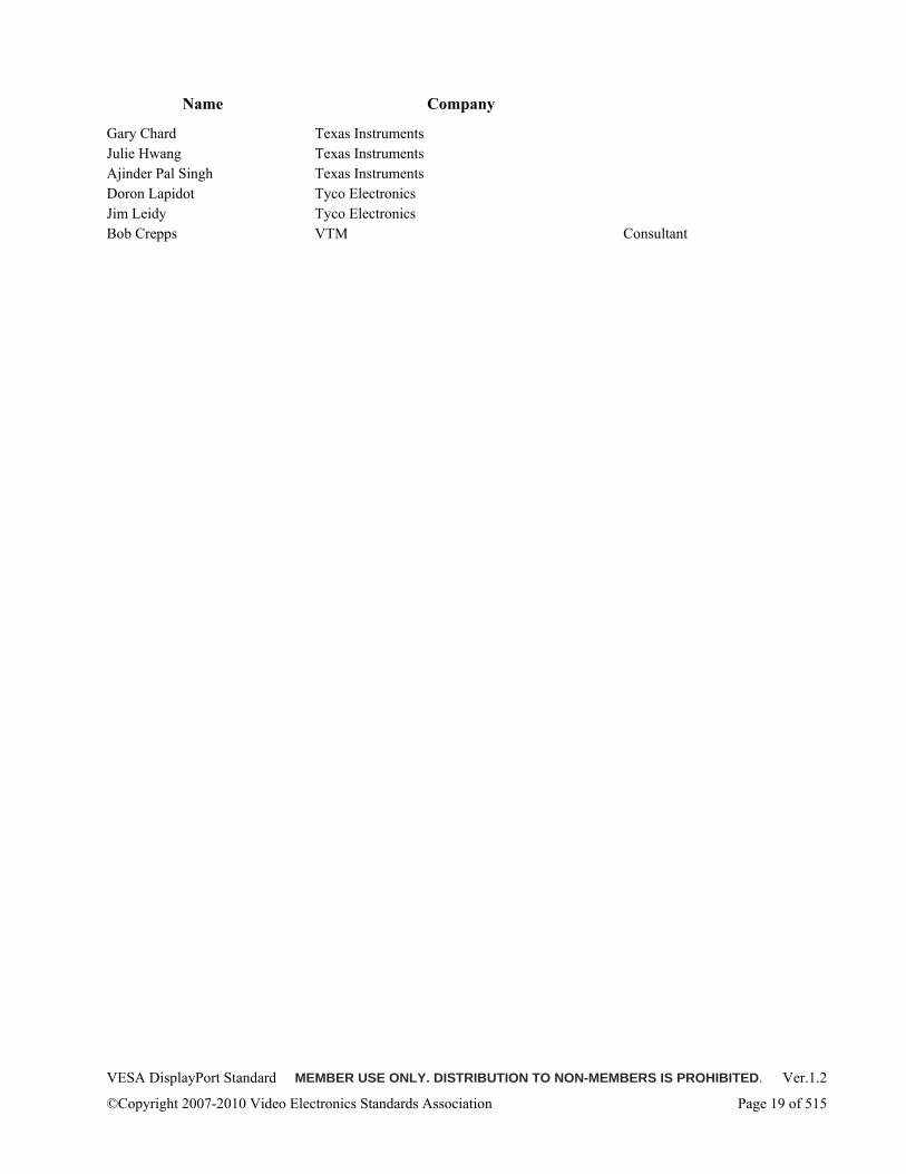
VESA DisplayPort Standard MEMBER USE ONLY. DISTRIBUTION TO NON-MEMBERS IS PROHIBITED. Ver.1.2
©Copyright 2007-2010 Video Electronics Standards Association Page 19 of 515
Name Company
Gary Chard Texas Instruments Julie Hwang Texas Instruments Ajinder Pal Singh Texas Instruments Doron Lapidot Tyco Electronics Jim Leidy Tyco Electronics Bob Crepps VTM Consultant
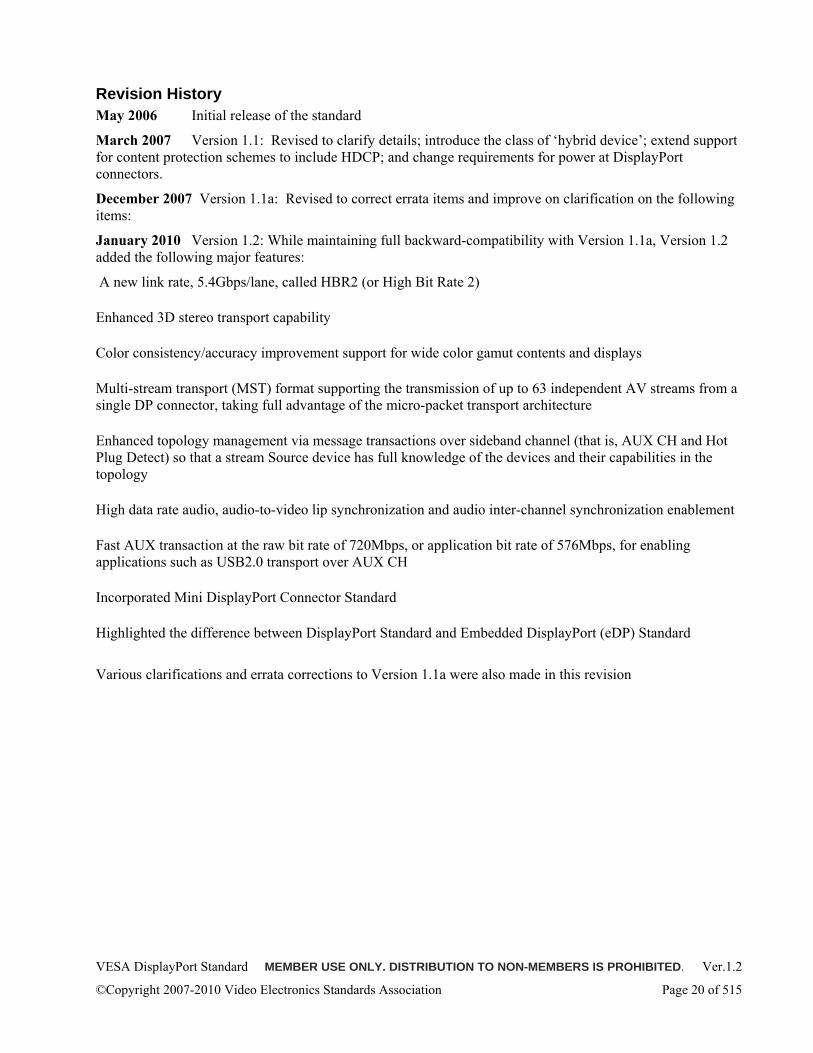
VESA DisplayPort Standard MEMBER USE ONLY. DISTRIBUTION TO NON-MEMBERS IS PROHIBITED. Ver.1.2
©Copyright 2007-2010 Video Electronics Standards Association Page 20 of 515
Revision History May 2006 Initial release of the standard
March 2007 Version 1.1: Revised to clarify details; introduce the class of ‘hybrid device’; extend support for content protection schemes to include HDCP; and change requirements for power at DisplayPort connectors.
December 2007 Version 1.1a: Revised to correct errata items and improve on clarification on the following items:
January 2010 Version 1.2: While maintaining full backward-compatibility with Version 1.1a, Version 1.2 added the following major features:
A new link rate, 5.4Gbps/lane, called HBR2 (or High Bit Rate 2)
Enhanced 3D stereo transport capability
Color consistency/accuracy improvement support for wide color gamut contents and displays
Multi-stream transport (MST) format supporting the transmission of up to 63 independent AV streams from a single DP connector, taking full advantage of the micro-packet transport architecture
Enhanced topology management via message transactions over sideband channel (that is, AUX CH and Hot Plug Detect) so that a stream Source device has full knowledge of the devices and their capabilities in the topology
High data rate audio, audio-to-video lip synchronization and audio inter-channel synchronization enablement
Fast AUX transaction at the raw bit rate of 720Mbps, or application bit rate of 576Mbps, for enabling applications such as USB2.0 transport over AUX CH
Incorporated Mini DisplayPort Connector Standard
Highlighted the difference between DisplayPort Standard and Embedded DisplayPort (eDP) Standard Various clarifications and errata corrections to Version 1.1a were also made in this revision
VESA DisplayPort Standard MEMBER USE ONLY. DISTRIBUTION TO NON-MEMBERS IS PROHIBITED. Ver.1.2
©Copyright 2007-2010 Video Electronics Standards Association Page 21 of 515
1 Introduction DisplayPort is an industry standard to accommodate the growing broad adoption of digital display technology within the PC and CE industries. It consolidates internal and external connection methods to reduce device complexity, supports necessary features for key cross industry applications, and provides performance scalability to enable the next generation of displays featuring higher color depths, refresh rates, and display resolutions.
1.1 DisplayPort Standard Organization The DisplayPort Standard is organized into the following sections that define the overall architecture and structure of the display interface:
Introduction
The introduction section defines the high level industry needs for DisplayPort, and the resulting technical objectives that the protocol, electrical, and mechanical sections are intended to satisfy. This section also includes a glossary of terms for the overall Standard, references, and overview of DisplayPort architecture.
Section 2 – Link Layer
The link layer section describes the protocol for configuring and managing the topology and the flow of data over both the forward (host to display) transport channel and the auxiliary bi-directional channel. Both SST (Single Stream Transport) mode and MST (Multi-Stream Transport) mode are covered.
Section 3 – PHY Layer
The physical layer section describes the electrical requirements of the DisplayPort transmitter and receiver implementations. It also defines the required circuitry and encoding methodology for transmitting data to and from the DisplayPort Link Layer over a cable or circuit board traces.
Section 4 – Mechanical
The mechanical section defines the connector and cable requirements for both internal and external DisplayPort connectors used to convey the electrical signals defined by the DisplayPort physical layer.
Section 5 – Source, Sink, Branch Devices Policy Requirements for Interoperability
The device and link media requirements section describes the policy requirements for Source, Sink, and Branch devices to support interoperability among devices that implement DisplayPort connections.
1.2 DisplayPort Objectives This Standard defines a scalable digital display interface with optional audio and content protection capability for broad application within PC and consumer electronic (CE) devices. The interface is designed to support both internal chip-to-chip and external box-to-box digital display connections. Potential internal chip-to-chip applications include usage within a notebook PC for driving a panel from a graphics controller, and usage within a monitor or TV for driving the display component from a display controller. Examples of box-to-box applications for DisplayPort include display connections between PCs and monitors, projectors, and TV displays. DisplayPort is also suitable for display connections between consumer electronics devices such as high-definition optical disc players, set top boxes, and television displays.
DisplayPort is designed to meet several key needs within the PC and CE industries as defined in Section 1.2.1. These industry needs are expanded into a set of technical objectives in Section 1.2.2 of the DisplayPort Standard to ensure that the display interface can support current and future industry requirements.
VESA DisplayPort Standard MEMBER USE ONLY. DISTRIBUTION TO NON-MEMBERS IS PROHIBITED. Ver.1.2
©Copyright 2007-2010 Video Electronics Standards Association Page 22 of 515
Specific objectives for external and internal display connections are defined in Sections 1.2.3 and 1.2.4 respectively of the DisplayPort Standard. Section 1.2.5 defines the additional objectives for CE devices applications.
1.2.1 Key Industry Needs for DisplayPort The following PC and CE industry needs were considered in the development of the DisplayPort architecture and resulting interface Standard:
1) Drive maximum application and re-use of digital technology to enable reduced device costs associated with implementing a digital display connection.
2) Enable a common signaling methodology for both internal and external display connections to reduce device complexity and promote commoditization.
3) Enable an extensible architecture that supports an optional robust content protection capability that may be economically implemented.
4) Enable high quality optional digital audio transmission capability.
5) Enable higher levels of silicon integration and innovation within rendering and display devices to reduce device complexity and enable digital interface commoditization. Examples of potential DisplayPort integration capability include transmitter integration within a graphics or display controller, and receiver integration within a timing controller on a module.
6) Simplify cabling for internal and external digital display connections.
7) Address performance concerns with existing technologies by providing higher bandwidth over fewer wires.
8) Apply embedded clock architecture to reduce electromagnetic interference (EMI) susceptibility and physical wire count.
9) Provide a small form factor connector that can be plugged in by feel, and a design that will enable four connectors to be placed on a full height Peripheral Component Interconnect (PCI) card bracket.
10) Enable broad PC and CE industry via an open and extensible industry standard.
DisplayPort addresses these industry needs by defining an electrical and protocol specification that may be readily implemented in module timing controllers, graphics processors, media processors, and display controllers.
A forward drive channel is defined that is scalable from one to four lanes, and implements a micro-packet architecture that supports variable color depths, refresh rates, and display pixel formats. A bi-directional auxiliary channel is defined that also implements micro-packet architecture for flexible delivery of control and status information.
DisplayPort includes a mechanical specification that defines a small, user-friendly external connector that is optimized for use on thin profile notebooks in addition to allowing up to four connectors on a graphics card. A standard module connector for internal applications is also defined in the mechanical section of this Standard.
1.2.2 DisplayPort Technical Objectives The cross-industry needs defined above for DisplayPort may be translated into specific technical objectives. These technical objectives for DisplayPort are to:
1) Provide a high bandwidth forward transmission link channel, with a bidirectional auxiliary channel capability.
VESA DisplayPort Standard MEMBER USE ONLY. DISTRIBUTION TO NON-MEMBERS IS PROHIBITED. Ver.1.2
©Copyright 2007-2010 Video Electronics Standards Association Page 23 of 515
2) Provide application support for up to 21.6Gbps (giga bits per second) forward link channel throughput to address long term PC industry needs to support greater than QXGA (2048x1536) pixel format and greater than 24-bit color depths.
3) Provide application support for 1Mbps (mega bit per second) auxiliary channel (AUX CH) throughput with a maximum latency of 500 micro-seconds in Manchester format, and optionally, 720Mbps in Fast AUX (FAUX) format over the AUX CH.
4) Support variable color depth transmission of 6, 8, 10, 12 or 16 bits per component
5) Support EMI compliance to FCC/CISPR B standard with a margin of at least 6db
6) Support existing VESA and CEA standards where applicable.
7) Architecture that does not preclude legacy transmission support (e.g. DVI and LVDS) to and from DisplayPort components.
8) Support hot plug and unplug detection and link status failure detection
9) Support full bandwidth transmission via direct drive over a two meter cable.
10) Support reduced bandwidth transmission via direct drive over a 15 meter cable. DisplayPort supports a minimum of 1080p lines at 24bpp, 50/60Hz over 4 lanes at 15 meters.
11) Support audio skew of less than 1ms
12) Support a bit error rate of 10-9 for raw transport per lane, and 10-12 symbol error rate for audio and control data after ECC encoding / decoding.
13) Support sub 65 nanometer (0.065 micron) process technologies for integration in Source devices, and supports 0.35 micron process technologies for integration in Sink devices.
1.2.3 DisplayPort External Connection Objectives For external connections between a Source device and a Sink device, this Standard is designed to achieve the following technical objectives:
1) Support reading of the display EDID (Extended Display Identification Data) whenever the display is connected to power, even trickle AC power.
2) Support DDC/CI (Display Data Channel/Command Interface) and MCCS (Monitor Command and Controls Set) command transmission.
3) Support external display configurations that do not include scaling, a discrete display controller, or on screen display (OSD) functions, enabling low cost, digital monitors.
4) For external notebook PC applications, DisplayPort allows support for direct drive through a docking connector configuration. A repeater function in the dock is strongly recommended.
5) The external DisplayPort connector is identical for all display applications and provides support for four lanes. Captive cables may support one, two or four lanes to reduce cost.
6) The external DisplayPort connector includes a multi-purpose power pin.
7) The external DisplayPort connector is symmetrical such that the same connector may be used on both source and Sink devices.
8) The external DisplayPort connector supports connection without the need for visual alignment.
9) The external DisplayPort connector is sized to allow four connectors to fit on a standard full height ATX/BTX bracket opening for PCI, AGP (Accelerated Graphics Port), and PCI-Express add in cards.
VESA DisplayPort Standard MEMBER USE ONLY. DISTRIBUTION TO NON-MEMBERS IS PROHIBITED. Ver.1.2
©Copyright 2007-2010 Video Electronics Standards Association Page 24 of 515
1.2.4 DisplayPort Internal Connection Objectives For internal connections such as within a notebook PC or display, this Standard is designed to achieve the following technical objectives:
1) DisplayPort defines a common module connector to simplify internal device connections.
2) The number of lanes in the internal cable is implementation dependent, and may be one, two or four.
3) Internal DisplayPort connections may support both maximum and reduced link bandwidths.
4) Internal DisplayPort connections support low link power modes.
5) Hot Plug support for internal DisplayPort connections is implementation dependent.
1.2.5 DisplayPort CE Connection Objectives For application to CE devices, this Standard is designed to address the following technical objectives:
1) DisplayPort optionally delivers digital audio data concurrent with display data.
2) Support for maintaining synchronization for delivery of audio and video data to within +/- 1ms.
3) DisplayPort architecture supports an optional robust content protection capability that may be economically implemented.
4) DisplayPort supports equivalent functionality to the feature sets defined in CEA-861-C for transmission of high quality uncompressed audio-video content, and CEA-931-B for the transport of remote control commands between Sink and Source devices.
5) DisplayPort supports variable audio formats, audio codings, sample frequencies, sample sizes, and audio channel configurations. DisplayPort supports up to eight channels of LPCM (Linear Pulse Code Modulation) audio at 192kHz with a 24-bit sample size.
6) DisplayPort supports variable video formats based on flexible aspect, pixel format, and refresh rate combinations based on the VESA DMT and CVT timing standards and those timing modes listed in the CEA-861-C standard.
7) DisplayPort supports industry-standard colorimetry specifications for CE devices including RGB and YCbCr 4:2:2 and YCbCr 4:4:4.
1.2.6 Content Protection for DisplayPort For implementations of the DisplayPort interface where content protection is desired, it is recommended that either DPCP (DisplayPort Content Protection) Version 1.0 or HDCP Version 1.3 be used. This is recommended in order to minimize incompatibilities between DisplayPort devices in the market.
1.3 Acronyms Table 1-1: List of Acronyms
Acronym Stands For:
ACT Allocation Change Trigger API Application Programming Interface. AUX Auxiliary BER Bit Error Rate bpc Bits Per Component bpp Bits Per Pixel BE Blanking End BS Blanking Start
VESA DisplayPort Standard MEMBER USE ONLY. DISTRIBUTION TO NON-MEMBERS IS PROHIBITED. Ver.1.2
©Copyright 2007-2010 Video Electronics Standards Association Page 25 of 515
Acronym Stands For:
CDR Clock and Data Recovery CEA Consumer Electronics Association CP Content Protection CVT Coordinated Video Timings (VESA) DB Data Byte DDC/CI Display Data Channel/Command Interface (VESA) DPCP DisplayPort Content Protection DPCD DisplayPort Configuration Data DJ Deterministic Jitter DMT Discrete Monitor Timing (VESA) DP DisplayPort (VESA) DPCD DisplayPort Configuration Data DP_PWR DP Power eDP Embedded DisplayPort (VESA) ECC Error Correcting Code ECF Encryption Control Field E-DDC Enhanced Display Data Channel (VESA) EDID Extended Display Identification Data (VESA) EOS Electrical Over-Stress EMT End of Message Transaction ESD Electro Static Discharge FAUX Fast AUX GPU Graphics Processor Unit GUID Globally Unique ID HB Header Byte HBR High Bit Rate (2.7Gbps per lane) HBR2 High Bit Rate 2 (5.4Gbps per lane) HDCP High-bandwidth Digital Content Protection HPD Hot Plug Detect I2C Inter-IC IRQ Interrupt Request ISI Inter-Symbol Interference LFSR Linear Feedback Shift Register. lsb Least Significant Bit LPCM Linear Pulse Code Modulation LVP Link Verification Pattern Maud M value for audio MCCS Monitor Control Command Set (VESA) msb Most Significant Bit MOT Middle Of Transaction MST Multi-Stream Transport MTP Multi-stream Transport Packet MTPH Multi-stream Transport Packet Header Mvid M value for video Naud N value for audio
VESA DisplayPort Standard MEMBER USE ONLY. DISTRIBUTION TO NON-MEMBERS IS PROHIBITED. Ver.1.2
©Copyright 2007-2010 Video Electronics Standards Association Page 26 of 515
Acronym Stands For:
nb Nibble Nvid N value for video NORP Number Of Receiver Ports OCP Over Current Protection OUI Organizational Unique ID PB Parity Byte PCB Printed Circuit Board PRBS Pseudo Random Bit Sequence RBR Reduced Bit Rate RG Rate Governing RGB Red Green Blue RJ Random Jitter RTL Register Transfer Level RX Receiver SDP Secondary-Data Packet SE SDP End SF Stream Fill SR Scrambler Reset SS SDP Start SSC Spread Spectrum Clock SST Single-Stream Transport TCON Timing Controller TDR Time Domain Reflectometry TIA Timing Interval Analyzer TIE Timing Interval Error TJ Total Jitter TU Transfer Unit TX Transmitter UI Unit Interval VB-ID Vertical Blanking ID VESA Video Electronics Standards Association
VHDL Very high speed integrated circuit Hardware Description Language
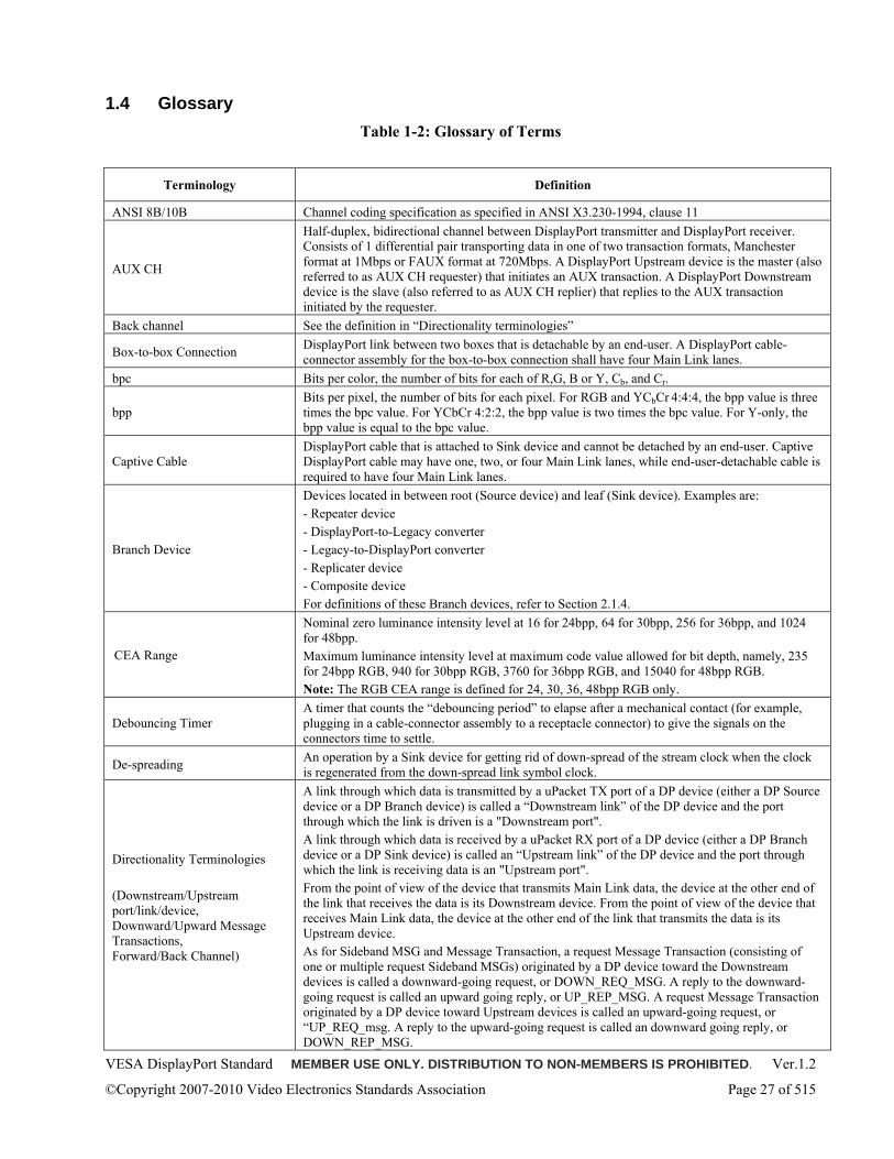
VESA DisplayPort Standard MEMBER USE ONLY. DISTRIBUTION TO NON-MEMBERS IS PROHIBITED. Ver.1.2
©Copyright 2007-2010 Video Electronics Standards Association Page 27 of 515
1.4 Glossary Table 1-2: Glossary of Terms
Terminology Definition
ANSI 8B/10B Channel coding specification as specified in ANSI X3.230-1994, clause 11
AUX CH
Half-duplex, bidirectional channel between DisplayPort transmitter and DisplayPort receiver. Consists of 1 differential pair transporting data in one of two transaction formats, Manchester format at 1Mbps or FAUX format at 720Mbps. A DisplayPort Upstream device is the master (also referred to as AUX CH requester) that initiates an AUX transaction. A DisplayPort Downstream device is the slave (also referred to as AUX CH replier) that replies to the AUX transaction initiated by the requester.
Back channel See the definition in “Directionality terminologies”
Box-to-box Connection DisplayPort link between two boxes that is detachable by an end-user. A DisplayPort cable-connector assembly for the box-to-box connection shall have four Main Link lanes.
bpc Bits per color, the number of bits for each of R,G, B or Y, Cb, and Cr.
bpp Bits per pixel, the number of bits for each pixel. For RGB and YCbCr 4:4:4, the bpp value is three times the bpc value. For YCbCr 4:2:2, the bpp value is two times the bpc value. For Y-only, the bpp value is equal to the bpc value.
Captive Cable DisplayPort cable that is attached to Sink device and cannot be detached by an end-user. Captive DisplayPort cable may have one, two, or four Main Link lanes, while end-user-detachable cable is required to have four Main Link lanes.
Branch Device
Devices located in between root (Source device) and leaf (Sink device). Examples are: - Repeater device - DisplayPort-to-Legacy converter - Legacy-to-DisplayPort converter - Replicater device - Composite device For definitions of these Branch devices, refer to Section 2.1.4.
CEA Range
Nominal zero luminance intensity level at 16 for 24bpp, 64 for 30bpp, 256 for 36bpp, and 1024 for 48bpp. Maximum luminance intensity level at maximum code value allowed for bit depth, namely, 235 for 24bpp RGB, 940 for 30bpp RGB, 3760 for 36bpp RGB, and 15040 for 48bpp RGB. Note: The RGB CEA range is defined for 24, 30, 36, 48bpp RGB only.
Debouncing Timer A timer that counts the “debouncing period” to elapse after a mechanical contact (for example, plugging in a cable-connector assembly to a receptacle connector) to give the signals on the connectors time to settle.
De-spreading An operation by a Sink device for getting rid of down-spread of the stream clock when the clock is regenerated from the down-spread link symbol clock.
Directionality Terminologies (Downstream/Upstream port/link/device, Downward/Upward Message Transactions, Forward/Back Channel)
A link through which data is transmitted by a uPacket TX port of a DP device (either a DP Source device or a DP Branch device) is called a “Downstream link” of the DP device and the port through which the link is driven is a "Downstream port". A link through which data is received by a uPacket RX port of a DP device (either a DP Branch device or a DP Sink device) is called an “Upstream link” of the DP device and the port through which the link is receiving data is an "Upstream port". From the point of view of the device that transmits Main Link data, the device at the other end of the link that receives the data is its Downstream device. From the point of view of the device that receives Main Link data, the device at the other end of the link that transmits the data is its Upstream device. As for Sideband MSG and Message Transaction, a request Message Transaction (consisting of one or multiple request Sideband MSGs) originated by a DP device toward the Downstream devices is called a downward-going request, or DOWN_REQ_MSG. A reply to the downward-going request is called an upward going reply, or UP_REP_MSG. A request Message Transaction originated by a DP device toward Upstream devices is called an upward-going request, or “UP_REQ_msg. A reply to the upward-going request is called an downward going reply, or DOWN_REP_MSG.
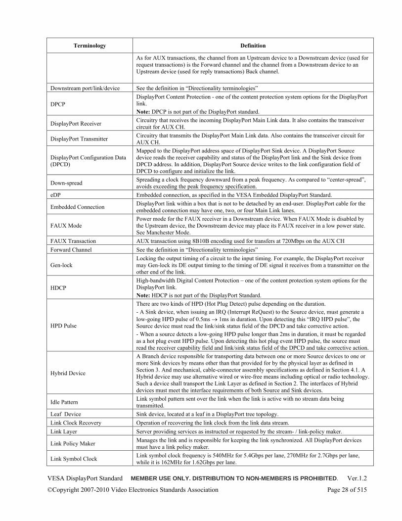
VESA DisplayPort Standard MEMBER USE ONLY. DISTRIBUTION TO NON-MEMBERS IS PROHIBITED. Ver.1.2
©Copyright 2007-2010 Video Electronics Standards Association Page 28 of 515
Terminology Definition
As for AUX transactions, the channel from an Upstream device to a Downstream device (used for request transactions) is the Forward channel and the channel from a Downstream device to an Upstream device (used for reply transactions) Back channel.
Downstream port/link/device See the definition in “Directionality terminologies”
DPCP DisplayPort Content Protection - one of the content protection system options for the DisplayPort link. Note: DPCP is not part of the DisplayPort standard.
DisplayPort Receiver Circuitry that receives the incoming DisplayPort Main Link data. It also contains the transceiver circuit for AUX CH.
DisplayPort Transmitter Circuitry that transmits the DisplayPort Main Link data. Also contains the transceiver circuit for AUX CH.
DisplayPort Configuration Data (DPCD)
Mapped to the DisplayPort address space of DisplayPort Sink device. A DisplayPort Source device reads the receiver capability and status of the DisplayPort link and the Sink device from DPCD address. In addition, DisplayPort Source device writes to the link configuration field of DPCD to configure and initialize the link.
Down-spread Spreading a clock frequency downward from a peak frequency. As compared to “center-spread”, avoids exceeding the peak frequency specification.
eDP Embedded connection, as specified in the VESA Embedded DisplayPort Standard.
Embedded Connection DisplayPort link within a box that is not to be detached by an end-user. DisplayPort cable for the embedded connection may have one, two, or four Main Link lanes.
FAUX Mode Power mode for the FAUX receiver in a Downstream device. When FAUX Mode is disabled by the Upstream device, the Downstream device may place its FAUX receiver in a low power state. See Manchester Mode.
FAUX Transaction AUX transaction using 8B10B encoding used for transfers at 720Mbps on the AUX CH Forward Channel See the definition in “Directionality terminologies”
Gen-lock Locking the output timing of a circuit to the input timing. For example, the DisplayPort receiver may Gen-lock its DE output timing to the timing of DE signal it receives from a transmitter on the other end of the link.
HDCP High-bandwidth Digital Content Protection – one of the content protection system options for the DisplayPort link. Note: HDCP is not part of the DisplayPort Standard.
HPD Pulse
There are two kinds of HPD (Hot Plug Detect) pulse depending on the duration. - A Sink device, when issuing an IRQ (Interrupt ReQuest) to the Source device, must generate a low-going HPD pulse of 0.5ms → 1ms in duration. Upon detecting this “IRQ HPD pulse”, the Source device must read the link/sink status field of the DPCD and take corrective action. - When a source detects a low-going HPD pulse longer than 2ms in duration, it must be regarded as a hot plug event HPD pulse. Upon detecting this hot plug event HPD pulse, the source must read the receiver capability field and link/sink status field of the DPCD and take corrective action.
Hybrid Device
A Branch device responsible for transporting data between one or more Source devices to one or more Sink devices by means other than that provided for by the physical layer as defined in Section 3. And mechanical, cable-connector assembly specifications as defined in Section 4.1. A Hybrid device may use alternative wired or wire-free means including optical or radio technology. Such a device shall transport the Link Layer as defined in Section 2. The interfaces of Hybrid devices must meet the interface requirements of both Source and Sink devices.
Idle Pattern Link symbol pattern sent over the link when the link is active with no stream data being transmitted.
Leaf Device Sink device, located at a leaf in a DisplayPort tree topology. Link Clock Recovery Operation of recovering the link clock from the link data stream. Link Layer Server providing services as instructed or requested by the stream- / link-policy maker.
Link Policy Maker Manages the link and is responsible for keeping the link synchronized. All DisplayPort devices must have a link policy maker.
Link Symbol Clock Link symbol clock frequency is 540MHz for 5.4Gbps per lane, 270MHz for 2.7Gbps per lane, while it is 162MHz for 1.62Gbps per lane.
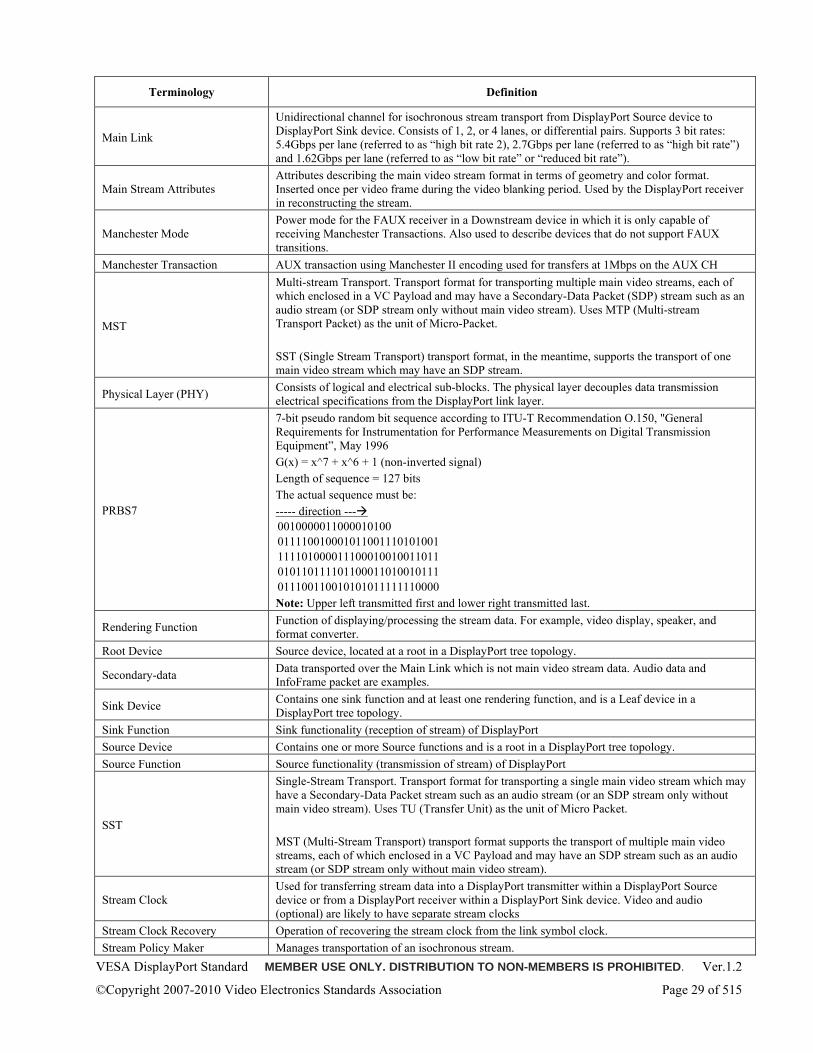
VESA DisplayPort Standard MEMBER USE ONLY. DISTRIBUTION TO NON-MEMBERS IS PROHIBITED. Ver.1.2
©Copyright 2007-2010 Video Electronics Standards Association Page 29 of 515
Terminology Definition
Main Link
Unidirectional channel for isochronous stream transport from DisplayPort Source device to DisplayPort Sink device. Consists of 1, 2, or 4 lanes, or differential pairs. Supports 3 bit rates: 5.4Gbps per lane (referred to as “high bit rate 2), 2.7Gbps per lane (referred to as “high bit rate”) and 1.62Gbps per lane (referred to as “low bit rate” or “reduced bit rate”).
Main Stream Attributes Attributes describing the main video stream format in terms of geometry and color format. Inserted once per video frame during the video blanking period. Used by the DisplayPort receiver in reconstructing the stream.
Manchester Mode Power mode for the FAUX receiver in a Downstream device in which it is only capable of receiving Manchester Transactions. Also used to describe devices that do not support FAUX transitions.
Manchester Transaction AUX transaction using Manchester II encoding used for transfers at 1Mbps on the AUX CH
MST
Multi-stream Transport. Transport format for transporting multiple main video streams, each of which enclosed in a VC Payload and may have a Secondary-Data Packet (SDP) stream such as an audio stream (or SDP stream only without main video stream). Uses MTP (Multi-stream Transport Packet) as the unit of Micro-Packet. SST (Single Stream Transport) transport format, in the meantime, supports the transport of one main video stream which may have an SDP stream.
Physical Layer (PHY) Consists of logical and electrical sub-blocks. The physical layer decouples data transmission electrical specifications from the DisplayPort link layer.
PRBS7
7-bit pseudo random bit sequence according to ITU-T Recommendation O.150, "General Requirements for Instrumentation for Performance Measurements on Digital Transmission Equipment”, May 1996 G(x) = x^7 + x^6 + 1 (non-inverted signal) Length of sequence = 127 bits The actual sequence must be: ----- direction --- 0010000011000010100 011110010001011001110101001 111101000011100010010011011 010110111101100011010010111 011100110010101011111110000 Note: Upper left transmitted first and lower right transmitted last.
Rendering Function Function of displaying/processing the stream data. For example, video display, speaker, and format converter.
Root Device Source device, located at a root in a DisplayPort tree topology.
Secondary-data Data transported over the Main Link which is not main video stream data. Audio data and InfoFrame packet are examples.
Sink Device Contains one sink function and at least one rendering function, and is a Leaf device in a DisplayPort tree topology.
Sink Function Sink functionality (reception of stream) of DisplayPort Source Device Contains one or more Source functions and is a root in a DisplayPort tree topology. Source Function Source functionality (transmission of stream) of DisplayPort
SST
Single-Stream Transport. Transport format for transporting a single main video stream which may have a Secondary-Data Packet stream such as an audio stream (or an SDP stream only without main video stream). Uses TU (Transfer Unit) as the unit of Micro Packet. MST (Multi-Stream Transport) transport format supports the transport of multiple main video streams, each of which enclosed in a VC Payload and may have an SDP stream such as an audio stream (or SDP stream only without main video stream).
Stream Clock Used for transferring stream data into a DisplayPort transmitter within a DisplayPort Source device or from a DisplayPort receiver within a DisplayPort Sink device. Video and audio (optional) are likely to have separate stream clocks
Stream Clock Recovery Operation of recovering the stream clock from the link symbol clock. Stream Policy Maker Manages transportation of an isochronous stream.
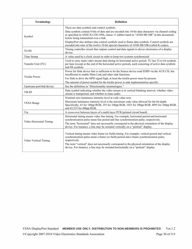
VESA DisplayPort Standard MEMBER USE ONLY. DISTRIBUTION TO NON-MEMBERS IS PROHIBITED. Ver.1.2
©Copyright 2007-2010 Video Electronics Standards Association Page 30 of 515
Terminology Definition
Symbol
There are data symbols and control symbols. Data symbols contain 8 bits of data and are encoded into 10-bit data characters via channel coding as specified in ANSI X3.230-1994, clause 11 (abbreviated as “ANSI 8B/10B” in this document) before being transmitted over a link. DisplayPort also defines nine control symbols used to frame data symbols. Control symbols are encoded into nine of the twelve 10-bit special characters of ANSI 8B/10B (called K-codes).
TCON Timing controller circuit that outputs control and data signals to driver electronics of a display device.
Time Stamp A value used by a clock circuit in order to keep two systems synchronized
Transfer Unit (TU) Used to carry main video stream data during its horizontal active period. TU has 32 to 64 symbols per lane (except at the end of the horizontal active period), each consisting of active data symbols and fill symbols.
Trickle Power
Power for Sink device that is sufficient to let the Source device read EDID via the AUX CH, but insufficient to enable Main Link and other sink functions. For Sink to drive the HPD signal high, at least the trickle power must be present. The amount of power needed for the trickle power is sink implementation specific.
Upstream port/link/device See the definition in “Directionality terminologies.”
VB-ID Data symbol indicating whether the video stream is in vertical blanking interval, whether video stream is transported, and whether to mute audio.
VESA Range
Nominal zero luminance intensity level at code value zero. Maximum luminance intensity level is the maximum code value allowed for the bit depth. Specifically, 63 for 18bpp RGB, 255 for 24bpp RGB, 1023 for 30bpp RGB, 4095 for 36bpp RGB, and 65,535 for 48bpp RGB.
Via A cross-over between layers of a multi-layer PCB (printed circuit board)
Video Horizontal Timing
Horizontal timing means video line timing. For example, horizontal period and horizontal synchronization pulse mean line period and line synchronization pulse, respectively. The term “horizontal” does not necessarily correspond to the physical orientation of the display device. For instance, a line may be oriented vertically on a “portrait” display.
Video Vertical Timing
Vertical timing means video frame (or field) timing. For example, vertical period and vertical synchronization pulse mean a frame (or field) period and a frame synchronization pulse, respectively. The term “vertical” does not necessarily correspond to the physical orientation of the display device. For instance, a line may be oriented horizontally on a “portrait” display.
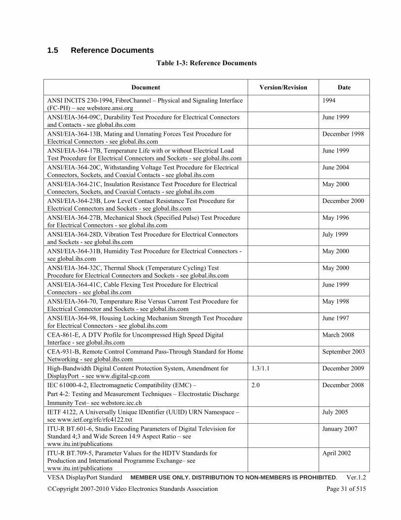
VESA DisplayPort Standard MEMBER USE ONLY. DISTRIBUTION TO NON-MEMBERS IS PROHIBITED. Ver.1.2
©Copyright 2007-2010 Video Electronics Standards Association Page 31 of 515
1.5 Reference Documents Table 1-3: Reference Documents
Document Version/Revision Date
ANSI INCITS 230-1994, FibreChannel – Physical and Signaling Interface (FC-PH) – see webstore.ansi.org
1994
ANSI/EIA-364-09C, Durability Test Procedure for Electrical Connectors and Contacts - see global.ihs.com
June 1999
ANSI/EIA-364-13B, Mating and Unmating Forces Test Procedure for Electrical Connectors - see global.ihs.com
December 1998
ANSI/EIA-364-17B, Temperature Life with or without Electrical Load Test Procedure for Electrical Connectors and Sockets - see global.ihs.com
June 1999
ANSI/EIA-364-20C, Withstanding Voltage Test Procedure for Electrical Connectors, Sockets, and Coaxial Contacts - see global.ihs.com
June 2004
ANSI/EIA-364-21C, Insulation Resistance Test Procedure for Electrical Connectors, Sockets, and Coaxial Contacts - see global.ihs.com
May 2000
ANSI/EIA-364-23B, Low Level Contact Resistance Test Procedure for Electrical Connectors and Sockets - see global.ihs.com
December 2000
ANSI/EIA-364-27B, Mechanical Shock (Specified Pulse) Test Procedure for Electrical Connectors - see global.ihs.com
May 1996
ANSI/EIA-364-28D, Vibration Test Procedure for Electrical Connectors and Sockets - see global.ihs.com
July 1999
ANSI/EIA-364-31B, Humidity Test Procedure for Electrical Connectors - see global.ihs.com
May 2000
ANSI/EIA-364-32C, Thermal Shock (Temperature Cycling) Test Procedure for Electrical Connectors and Sockets - see global.ihs.com
May 2000
ANSI/EIA-364-41C, Cable Flexing Test Procedure for Electrical Connectors - see global.ihs.com
June 1999
ANSI/EIA-364-70, Temperature Rise Versus Current Test Procedure for Electrical Connector and Sockets - see global.ihs.com
May 1998
ANSI/EIA-364-98, Housing Locking Mechanism Strength Test Procedure for Electrical Connectors - see global.ihs.com
June 1997
CEA-861-E, A DTV Profile for Uncompressed High Speed Digital Interface - see global.ihs.com
March 2008
CEA-931-B, Remote Control Command Pass-Through Standard for Home Networking - see global.ihs.com
September 2003
High-Bandwidth Digital Content Protection System, Amendment for DisplayPort - see www.digital-cp.com
1.3/1.1 December 2009
IEC 61000-4-2, Electromagnetic Compatibility (EMC) – Part 4-2: Testing and Measurement Techniques – Electrostatic Discharge Immunity Test– see webstore.iec.ch
2.0 December 2008
IETF 4122, A Universally Unique IDentifier (UUID) URN Namespace – see www.ietf.org/rfc/rfc4122.txt
July 2005
ITU-R BT.601-6, Studio Encoding Parameters of Digital Television for Standard 4;3 and Wide Screen 14:9 Aspect Ratio – see www.itu.int/publications
January 2007
ITU-R BT.709-5, Parameter Values for the HDTV Standards for Production and International Programme Exchange– see www.itu.int/publications
April 2002
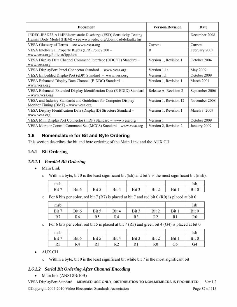
VESA DisplayPort Standard MEMBER USE ONLY. DISTRIBUTION TO NON-MEMBERS IS PROHIBITED. Ver.1.2
©Copyright 2007-2010 Video Electronics Standards Association Page 32 of 515
Document Version/Revision Date
JEDEC JESD22-A114FElectrostatic Discharge (ESD) Sensitivity Testing Human Body Model (HBM) – see www.jedec.org/download/default.cfm
December 2008
VESA Glossary of Terms – see www.vesa.org Current Current VESA Intellectual Property Rights (IPR) Policy 200 – www.vesa.org/Policies/ipp.htm
B February 2005
VESA Display Data Channel Command Interface (DDC/CI) Standard – www.vesa.org
Version 1, Revision 1 October 2004
VESA DisplayPort Panel Connector Standard – www.vesa.org Version 1.1a May 2009 VESA Embedded DisplayPort (eDP) Standard – www.vesa.org Version 1.1 October 2009 VESA Enhanced Display Data Channel (E-DDC) Standard – www.vesa.org
Version 1, Revision 1 March 2004
VESA Enhanced Extended Display Identification Data (E-EDID) Standard – www.vesa.org
Release A, Revision 2 September 2006
VESA and Industry Standards and Guidelines for Computer Display Monitor Timing (DMT) – www.vesa.org
Version 1, Revision 12 November 2008
VESA Display Identification Data (DisplayID) Structure Standard – www.vesa.org
Version 1, Revision 1 March 3, 2009
VESA Mini DisplayPort Connector (mDP) Standard – www.vesa.org Version 1 October 2009 VESA Monitor Control Command Set (MCCS) Standard – www.vesa.org Version 2, Revision 2 January 2009
1.6 Nomenclature for Bit and Byte Ordering This section describes the bit and byte ordering of the Main Link and the AUX CH.
1.6.1 Bit Ordering
1.6.1.1 Parallel Bit Ordering • Main Link
o Within a byte, bit 0 is the least significant bit (lsb) and bit 7 is the most significant bit (msb).
msb lsb Bit 7 Bit 6 Bit 5 Bit 4 Bit 3 Bit 2 Bit 1 Bit 0
o For 8 bits per color, red bit 7 (R7) is placed at bit 7 and red bit 0 (R0) is placed at bit 0
msb lsb Bit 7 Bit 6 Bit 5 Bit 4 Bit 3 Bit 2 Bit 1 Bit 0 R7 R6 R5 R4 R3 R2 R1 R0
o For 6 bits per color, red bit 5 is placed at bit 7 (R5) and green bit 4 (G4) is placed at bit 0
msb lsb Bit 7 Bit 6 Bit 5 Bit 4 Bit 3 Bit 2 Bit 1 Bit 0 R5 R4 R3 R2 R1 R0 G5 G4
• AUX CH
o Within a byte, bit 0 is the least significant bit while bit 7 is the most significant bit
1.6.1.2 Serial Bit Ordering After Channel Encoding • Main link (ANSI 8B/10B)
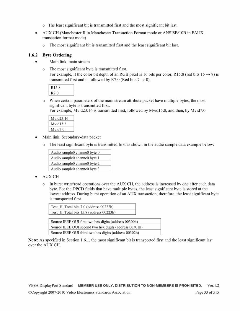
VESA DisplayPort Standard MEMBER USE ONLY. DISTRIBUTION TO NON-MEMBERS IS PROHIBITED. Ver.1.2
©Copyright 2007-2010 Video Electronics Standards Association Page 33 of 515
o The least significant bit is transmitted first and the most significant bit last.
• AUX CH (Manchester II in Manchester Transaction Format mode or ANSI8B/10B in FAUX transaction format mode)
o The most significant bit is transmitted first and the least significant bit last.
1.6.2 Byte Ordering • Main link, main stream
o The most significant byte is transmitted first. For example, if the color bit depth of an RGB pixel is 16 bits per color, R15:8 (red bits 15 → 8) is transmitted first and is followed by R7:0 (Red bits 7 → 0).
R15:8 R7:0
o When certain parameters of the main stream attribute packet have multiple bytes, the most significant byte is transmitted first. For example, Mvid23:16 is transmitted first, followed by Mvid15:8, and then, by Mvid7:0.
Mvid23:16 Mvid15:8 Mvid7:0
• Main link, Secondary-data packet
o The least significant byte is transmitted first as shown in the audio sample data example below.
Audio sample0 channe0 byte 0 Audio sample0 channe0 byte 1 Audio sample0 channe0 byte 2 Audio sample0 channe0 byte 3
• AUX CH
o In burst write/read operations over the AUX CH, the address is increased by one after each data byte. For the DPCD fields that have multiple bytes, the least significant byte is stored at the lowest address. During burst operation of an AUX transaction, therefore, the least significant byte is transported first.
Test_H_Total bits 7:0 (address 00222h) Test_H_Total bits 15:8 (address 00223h)
Source IEEE OUI first two hex digits (address 00300h) Source IEEE OUI second two hex digits (address 00301h) Source IEEE OUI third two hex digits (address 00302h)
Note: As specified in Section 1.6.1, the most significant bit is transported first and the least significant last over the AUX CH.
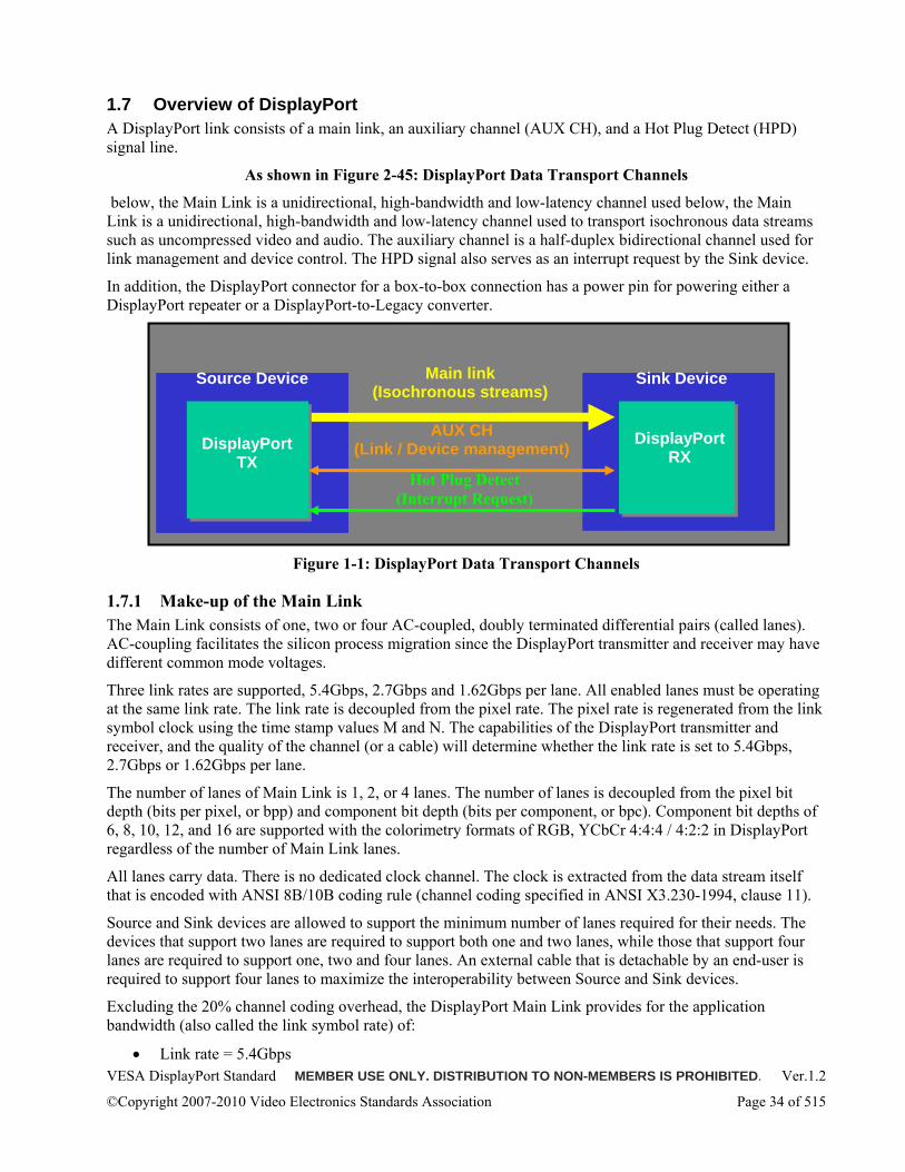
VESA DisplayPort Standard MEMBER USE ONLY. DISTRIBUTION TO NON-MEMBERS IS PROHIBITED. Ver.1.2
©Copyright 2007-2010 Video Electronics Standards Association Page 34 of 515
1.7 Overview of DisplayPort A DisplayPort link consists of a main link, an auxiliary channel (AUX CH), and a Hot Plug Detect (HPD) signal line.
As shown in Figure 2-45: DisplayPort Data Transport Channels
below, the Main Link is a unidirectional, high-bandwidth and low-latency channel used below, the Main Link is a unidirectional, high-bandwidth and low-latency channel used to transport isochronous data streams such as uncompressed video and audio. The auxiliary channel is a half-duplex bidirectional channel used for link management and device control. The HPD signal also serves as an interrupt request by the Sink device.
In addition, the DisplayPort connector for a box-to-box connection has a power pin for powering either a DisplayPort repeater or a DisplayPort-to-Legacy converter.
Figure 1-1: DisplayPort Data Transport Channels
1.7.1 Make-up of the Main Link The Main Link consists of one, two or four AC-coupled, doubly terminated differential pairs (called lanes). AC-coupling facilitates the silicon process migration since the DisplayPort transmitter and receiver may have different common mode voltages.
Three link rates are supported, 5.4Gbps, 2.7Gbps and 1.62Gbps per lane. All enabled lanes must be operating at the same link rate. The link rate is decoupled from the pixel rate. The pixel rate is regenerated from the link symbol clock using the time stamp values M and N. The capabilities of the DisplayPort transmitter and receiver, and the quality of the channel (or a cable) will determine whether the link rate is set to 5.4Gbps, 2.7Gbps or 1.62Gbps per lane.
The number of lanes of Main Link is 1, 2, or 4 lanes. The number of lanes is decoupled from the pixel bit depth (bits per pixel, or bpp) and component bit depth (bits per component, or bpc). Component bit depths of 6, 8, 10, 12, and 16 are supported with the colorimetry formats of RGB, YCbCr 4:4:4 / 4:2:2 in DisplayPort regardless of the number of Main Link lanes.
All lanes carry data. There is no dedicated clock channel. The clock is extracted from the data stream itself that is encoded with ANSI 8B/10B coding rule (channel coding specified in ANSI X3.230-1994, clause 11).
Source and Sink devices are allowed to support the minimum number of lanes required for their needs. The devices that support two lanes are required to support both one and two lanes, while those that support four lanes are required to support one, two and four lanes. An external cable that is detachable by an end-user is required to support four lanes to maximize the interoperability between Source and Sink devices.
Excluding the 20% channel coding overhead, the DisplayPort Main Link provides for the application bandwidth (also called the link symbol rate) of:
• Link rate = 5.4Gbps
DisplayPort TX
DisplayPort RX
Main link (Isochronous streams)
Sink Device
AUX CH (Link / Device management)
Hot Plug Detect (Interrupt Request)
Source Device
VESA DisplayPort Standard MEMBER USE ONLY. DISTRIBUTION TO NON-MEMBERS IS PROHIBITED. Ver.1.2
©Copyright 2007-2010 Video Electronics Standards Association Page 35 of 515
o 1 lane = 540Mbytes per second
o 2 lanes = 1080Mbytes per second
o 4 lanes = 2160Mbytes per second
• Link rate = 2.7Gbps
o 1 lane = 270Mbytes per second
o 2 lanes = 540Mbytes per second
o 4 lanes = 1080Mbytes per second
• Link rate = 1.62Gbps
o 1 lane = 162Mbytes per second
o 2 lanes = 324Mbytes per second
o 4 lanes = 648Mbytes per second
DisplayPort devices may freely trade pixel bit depth with pixel format and the frame rate of a stream within the available bandwidth.
The data mapping of a stream to the Main Link is devised to facilitate the support of various lane counts. For example, the pixel data is packed and mapped over a four lane Main Link as follows, regardless of the pixel bit depth and colorimetry format:
• Pixel data mapping over a four lane Main Link
o Pixels 0, 4 : Lane 0,
o Pixels 1, 5 : Lane 1
o Pixels 2, 6 : Lane 2
o Pixels 3, 7 : Lane 3
The stream data is packed into “micro-packets” which are called “transfer units” in SST (Single Stream Transport) mode and MTP (Multi-stream Transport Packet) in MST (Multi-Stream Transport) mode. After the stream data is packed and mapped to main link, the packed stream data rate will be equal to or smaller than the link symbol rate of the main link. When it is smaller, stuffing symbols are inserted.
1.7.2 Make-up of AUX CH AUX CH consists of an AC-coupled, doubly-terminated differential pair. Manchester-II coding is used as the channel coding for the AUX CH. As is the case with main link, the clock is extracted from the data stream.
AUX CH is half-duplex, bidirectional. The Source device is the master and the Sink device the slave. A Sink device may toggle the HPD signal to interrupt the Source device which would prompt an AUX CH request transaction.
AUX CH provides a data rate of 1Mbps over the supported cable lengths of up to 15m and longer. Each transaction takes no more than 500us with a maximum burst data size of 16 bytes. This avoids AUX CH contention problems by one application starving other applications.
AUC CH in Fast AUX transaction format provides a data rate of 720Mb/s over HBR (high bit rate) cable.
1.7.3 Link Configuration and Management Upon Hot Plug detection, the Source device configures the link through link training. The correct number of lanes is enabled at the correct link rate with the correct drive current and equalization level through the handshake between DisplayPort transmitter and receiver via AUX CH.
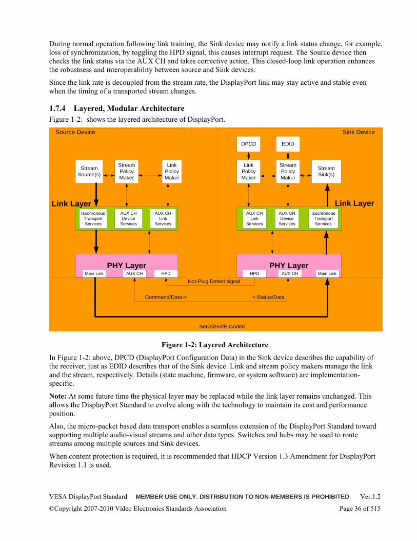
VESA DisplayPort Standard MEMBER USE ONLY. DISTRIBUTION TO NON-MEMBERS IS PROHIBITED. Ver.1.2
©Copyright 2007-2010 Video Electronics Standards Association Page 36 of 515
During normal operation following link training, the Sink device may notify a link status change, for example, loss of synchronization, by toggling the HPD signal, this causes interrupt request. The Source device then checks the link status via the AUX CH and takes corrective action. This closed-loop link operation enhances the robustness and interoperability between source and Sink devices.
Since the link rate is decoupled from the stream rate, the DisplayPort link may stay active and stable even when the timing of a transported stream changes.
1.7.4 Layered, Modular Architecture Figure 1-2: shows the layered architecture of DisplayPort.
StreamSource(s)
StreamPolicyMaker
StreamSink(s)
StreamPolicyMaker
PHY LayerHPDAUX CHMain Link
PHY LayerMain LinkAUX CHHPD
Serialized/Encoded
Hot-Plug Detect signal
Command/Data-> <-Status/Data
EDIDDPCD
Source Device Sink Device
LinkPolicyMaker
IsochronousTransportServices
AUX CHDevice
Services
AUX CHLink
Services
IsochronousTransportServices
AUX CHLink
Services
AUX CHDevice
Services
Link Layer Link Layer
LinkPolicyMaker
Figure 1-2: Layered Architecture
In Figure 1-2: above, DPCD (DisplayPort Configuration Data) in the Sink device describes the capability of the receiver, just as EDID describes that of the Sink device. Link and stream policy makers manage the link and the stream, respectively. Details (state machine, firmware, or system software) are implementation-specific.
Note: At some future time the physical layer may be replaced while the link layer remains unchanged. This allows the DisplayPort Standard to evolve along with the technology to maintain its cost and performance position.
Also, the micro-packet based data transport enables a seamless extension of the DisplayPort Standard toward supporting multiple audio-visual streams and other data types. Switches and hubs may be used to route streams among multiple sources and Sink devices.
When content protection is required, it is recommended that HDCP Version 1.3 Amendment for DisplayPort Revision 1.1 is used.
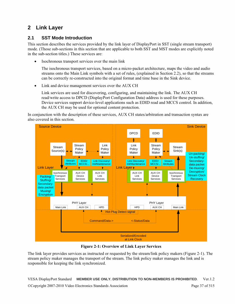
VESA DisplayPort Standard MEMBER USE ONLY. DISTRIBUTION TO NON-MEMBERS IS PROHIBITED. Ver.1.2
©Copyright 2007-2010 Video Electronics Standards Association Page 37 of 515
2 Link Layer
2.1 SST Mode Introduction This section describes the services provided by the link layer of DisplayPort in SST (single stream transport) mode. (Those sub-sections in this section that are applicable to both SST and MST modes are explicitly noted in the sub-section titles.) These services are:
• Isochronous transport services over the main link
The isochronous transport services, based on a micro-packet architecture, maps the video and audio streams onto the Main Link symbols with a set of rules, (explained in Section 2.2), so that the streams can be correctly re-constructed into the original format and time base in the Sink device.
• Link and device management services over the AUX CH
Link services are used for discovering, configuring, and maintaining the link. The AUX CH read/write access to DPCD (DisplayPort Configuration Data) address is used for these purposes. Device services support device-level applications such as EDID read and MCCS control. In addition, the AUX CH may be used for optional content protection.
In conjunction with the description of these services, AUX CH states/arbitration and transaction syntax are also covered in this section.
StreamSource(s)
StreamPolicyMaker
StreamSink(s)
StreamPolicyMaker
PHY LayerHPDAUX CHMain Link
PHY LayerMain LinkAUX CHHPD
Serialized/Encodedat Link Clock
Hot-Plug Detect signal
Command/Data-> <-Status/Data
EDIDDPCD
Source Device Sink Device
LinkPolicyMaker
IsochronousTransportServices
AUX CHDevice
Services
AUX CHLink
Services
IsochronousTransportServices
AUX CHLink
Services
AUX CHDevice
Services
Link Discovery/Init/Maintenance
EDID/MCCS/...
Packing/Stuffing/
Secondary-data packet
Muxing/Encryption
Un-packing/Un-stuffing/Secondary-data packetDe-muxing/Decryption/
Stream ClockRecovery
EDID/MCCS/...
Link Layer Link Layer
LinkPolicyMaker
Link Discovery/Init/Maintenance
SttreamAttributes
StreamAttributes
Figure 2-1: Overview of Link Layer Services
The link layer provides services as instructed or requested by the stream/link policy makers (Figure 2-1). The stream policy maker manages the transport of the stream. The link policy maker manages the link and is responsible for keeping the link synchronized.
VESA DisplayPort Standard MEMBER USE ONLY. DISTRIBUTION TO NON-MEMBERS IS PROHIBITED. Ver.1.2
©Copyright 2007-2010 Video Electronics Standards Association Page 38 of 515
In this section (and in the entire DisplayPort Standard), only the interactions between the policy makers and the link layer are described. The syntax for these interactions (that is, the API) is implementation-specific, and beyond the scope of this document.
2.1.1 Number of Lanes and Per-lane Data Rate (Applicable both in SST and MST Modes) DisplayPort supports three options for the number of Main Link lanes and two options for Main Link data rate per lane as follows:
• 4-, 2-, or 1-lane
• 5.4Gbps, 2.7Gbps or 1.62Gbps per lane
The link layer specification and data mapping specification in particular, is defined to facilitate the support of these lane count options.
The per lane data rate is determined not only by the capabilities of DisplayPort transmitter and receiver but also by the quality of a channel, or a cable.
The DisplayPort Sink device must indicate the capability of its receiver in the receiver capability field of the DPCD, as described.
After reading the receiver capability, the DisplayPort Source device must configure the link by writing to the link configuration field of the DPCD in the DisplayPort Sink device and then running link training.
Through this process of receiver capability discovery and link training, the DisplayPort Source and Sink devices are able to negotiate for the optimal lane count and per lane data rate for a given connection.
2.1.2 Number of Main, Uncompressed Video Streams in SST Mode The scope of DisplayPort Standard is limited to the transport of a single, uncompressed video stream as the main stream, with the optional insertion of secondary-data packets such as an audio stream packet.
2.1.3 Basic Functions (Applicable both in SST and MST Modes) The basic functions of DisplayPort devices are described below.
• uPacket TX function – Functionality of Main Link symbol transmission
• uPacket RX function – Functionality of Main Link symbol reception
• Stream Source/Sink function – Functionality of sourcing and sinking of streams
2.1.4 DisplayPort Device Types and Link Topology in SST Mode A device will contain at least one DisplayPort function as well as other functions such as a display, speakers, recording device or even an entire computer.
The DisplayPort Standard covers the following device types:
• Source device - a device that contains one or more stream source functions and uPacket TX functions and is a root in a DisplayPort tree topology.
• Sink device – a device that contains one or more uPacket RX functions and one or more stream sink functions and is a leaf in a DisplayPort topology.
• Repeater device (one input, one output) – a device that contains one DisplayPort uPacket RX function and one DisplayPort uPacket TX function.
• Legacy-to-DisplayPort Converter (one input, one output) – a device that contains one legacy RX function and one DisplayPort uPacket TX function.
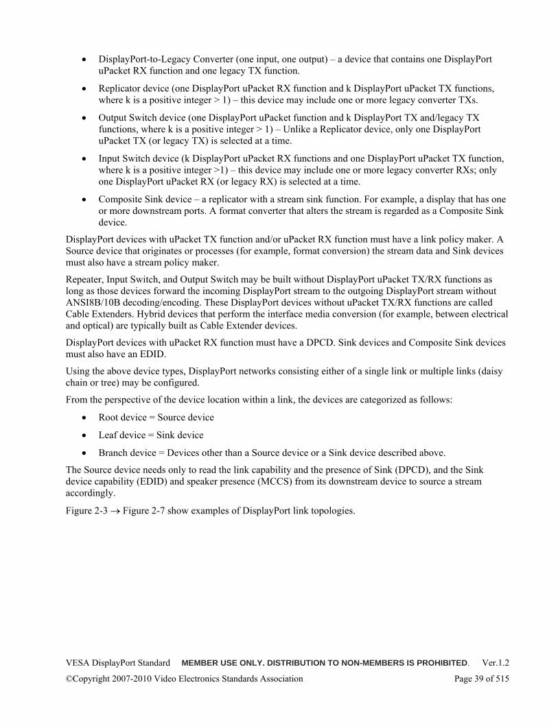
VESA DisplayPort Standard MEMBER USE ONLY. DISTRIBUTION TO NON-MEMBERS IS PROHIBITED. Ver.1.2
©Copyright 2007-2010 Video Electronics Standards Association Page 39 of 515
• DisplayPort-to-Legacy Converter (one input, one output) – a device that contains one DisplayPort uPacket RX function and one legacy TX function.
• Replicator device (one DisplayPort uPacket RX function and k DisplayPort uPacket TX functions, where k is a positive integer > 1) – this device may include one or more legacy converter TXs.
• Output Switch device (one DisplayPort uPacket function and k DisplayPort TX and/legacy TX functions, where k is a positive integer > 1) – Unlike a Replicator device, only one DisplayPort uPacket TX (or legacy TX) is selected at a time.
• Input Switch device (k DisplayPort uPacket RX functions and one DisplayPort uPacket TX function, where k is a positive integer >1) – this device may include one or more legacy converter RXs; only one DisplayPort uPacket RX (or legacy RX) is selected at a time.
• Composite Sink device – a replicator with a stream sink function. For example, a display that has one or more downstream ports. A format converter that alters the stream is regarded as a Composite Sink device.
DisplayPort devices with uPacket TX function and/or uPacket RX function must have a link policy maker. A Source device that originates or processes (for example, format conversion) the stream data and Sink devices must also have a stream policy maker.
Repeater, Input Switch, and Output Switch may be built without DisplayPort uPacket TX/RX functions as long as those devices forward the incoming DisplayPort stream to the outgoing DisplayPort stream without ANSI8B/10B decoding/encoding. These DisplayPort devices without uPacket TX/RX functions are called Cable Extenders. Hybrid devices that perform the interface media conversion (for example, between electrical and optical) are typically built as Cable Extender devices.
DisplayPort devices with uPacket RX function must have a DPCD. Sink devices and Composite Sink devices must also have an EDID.
Using the above device types, DisplayPort networks consisting either of a single link or multiple links (daisy chain or tree) may be configured.
From the perspective of the device location within a link, the devices are categorized as follows:
• Root device = Source device
• Leaf device = Sink device
• Branch device = Devices other than a Source device or a Sink device described above.
The Source device needs only to read the link capability and the presence of Sink (DPCD), and the Sink device capability (EDID) and speaker presence (MCCS) from its downstream device to source a stream accordingly.
Figure 2-3 → Figure 2-7 show examples of DisplayPort link topologies.
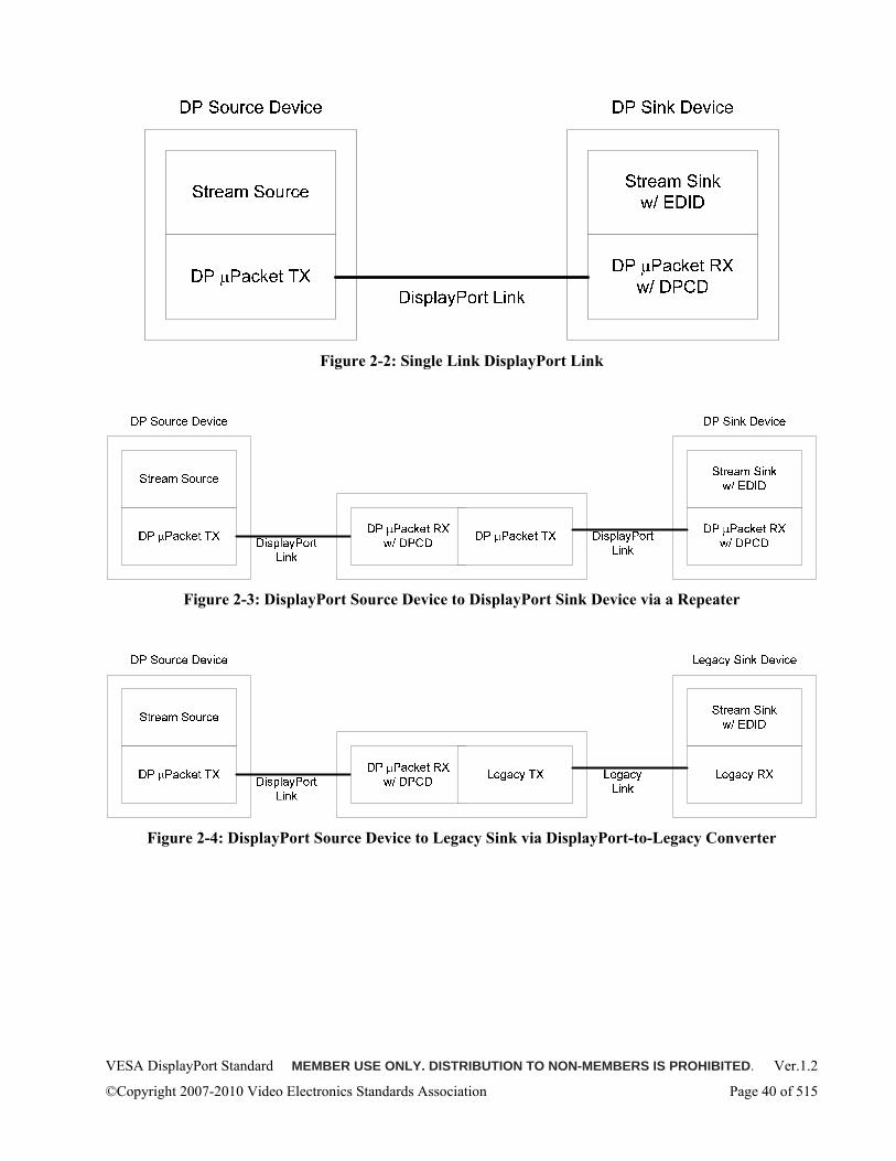
VESA DisplayPort Standard MEMBER USE ONLY. DISTRIBUTION TO NON-MEMBERS IS PROHIBITED. Ver.1.2
©Copyright 2007-2010 Video Electronics Standards Association Page 40 of 515
Figure 2-2: Single Link DisplayPort Link
Figure 2-3: DisplayPort Source Device to DisplayPort Sink Device via a Repeater
Figure 2-4: DisplayPort Source Device to Legacy Sink via DisplayPort-to-Legacy Converter
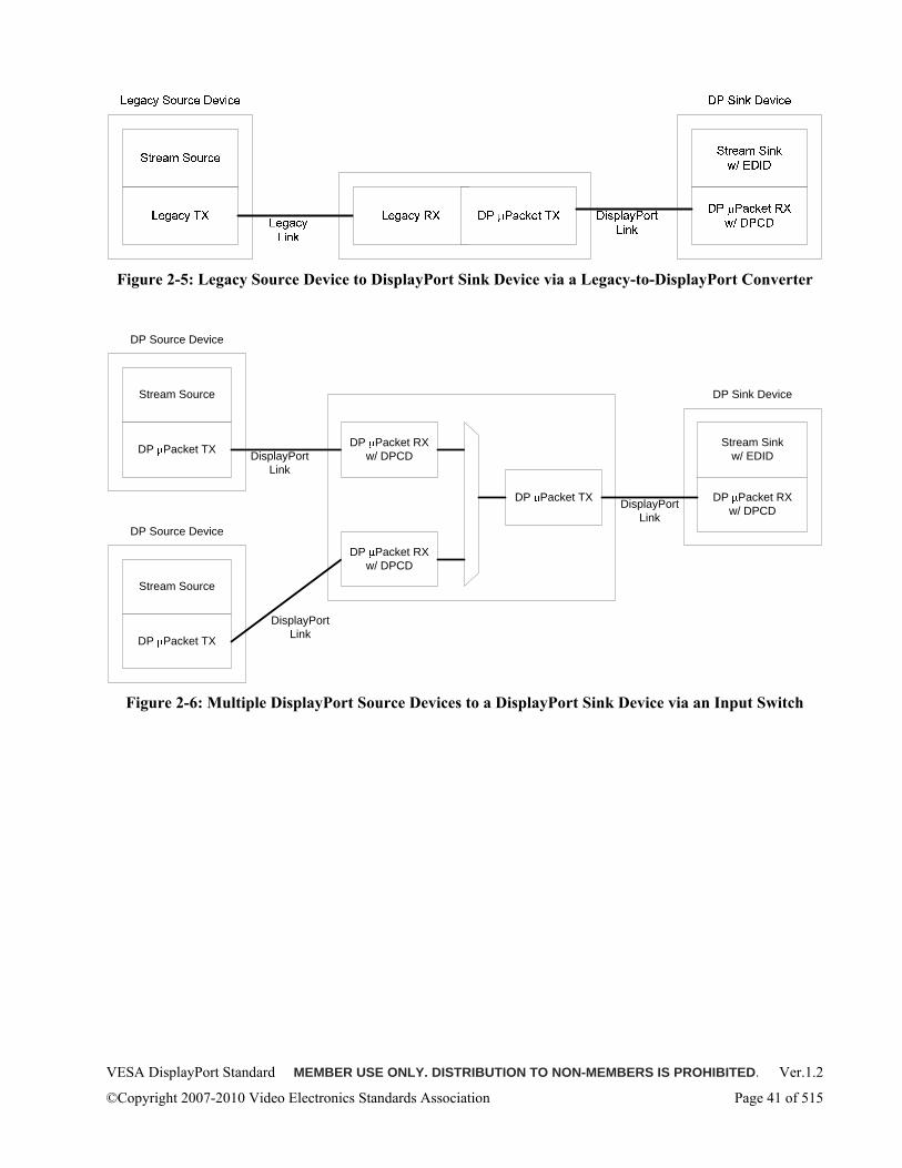
VESA DisplayPort Standard MEMBER USE ONLY. DISTRIBUTION TO NON-MEMBERS IS PROHIBITED. Ver.1.2
©Copyright 2007-2010 Video Electronics Standards Association Page 41 of 515
Figure 2-5: Legacy Source Device to DisplayPort Sink Device via a Legacy-to-DisplayPort Converter
Stream Source
DP Packet TX Stream Sinkw/ EDID
DP Packet RXw/ DPCD
DisplayPort Link
DP Source Device
DP Sink Device
DP Packet RXw/ DPCD
DP Packet TX DisplayPort Link
Stream Source
DP Packet TX
DisplayPort Link
DP Source Device
DP Packet RXw/ DPCD
Figure 2-6: Multiple DisplayPort Source Devices to a DisplayPort Sink Device via an Input Switch
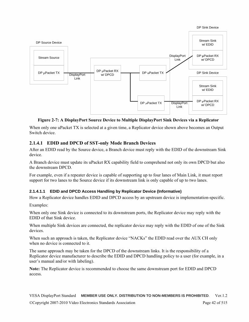
VESA DisplayPort Standard MEMBER USE ONLY. DISTRIBUTION TO NON-MEMBERS IS PROHIBITED. Ver.1.2
©Copyright 2007-2010 Video Electronics Standards Association Page 42 of 515
Stream Source
DP Packet TX
Stream Sinkw/ EDID
DP Packet RXw/ DPCD
DisplayPort Link
DP Source Device
DP Sink Device
DP Packet RXw/ DPCD DP Packet TX
DisplayPort Link
DP Packet TX
Stream Sinkw/ EDID
DP Packet RXw/ DPCD
DP Sink Device
DisplayPort Link
Figure 2-7: A DisplayPort Source Device to Multiple DisplayPort Sink Devices via a Replicator
When only one uPacket TX is selected at a given time, a Replicator device shown above becomes an Output Switch device.
2.1.4.1 EDID and DPCD of SST-only Mode Branch Devices After an EDID read by the Source device, a Branch device must reply with the EDID of the downstream Sink device.
A Branch device must update its uPacket RX capability field to comprehend not only its own DPCD but also the downstream DPCD.
For example, even if a repeater device is capable of supporting up to four lanes of Main Link, it must report support for two lanes to the Source device if its downstream link is only capable of up to two lanes.
2.1.4.1.1 EDID and DPCD Access Handling by Replicator Device (Informative) How a Replicator device handles EDID and DPCD access by an upstream device is implementation-specific.
Examples:
When only one Sink device is connected to its downstream ports, the Replicator device may reply with the EDID of that Sink device.
When multiple Sink devices are connected, the replicator device may reply with the EDID of one of the Sink devices.
When such an approach is taken, the Replicator device “NACKs” the EDID read over the AUX CH only when no device is connected to it.
The same approach may be taken for the DPCD of the downstream links. It is the responsibility of a Replicator device manufacturer to describe the EDID and DPCD handling policy to a user (for example, in a user’s manual and/or with labeling).
Note: The Replicator device is recommended to choose the same downstream port for EDID and DPCD access.
VESA DisplayPort Standard MEMBER USE ONLY. DISTRIBUTION TO NON-MEMBERS IS PROHIBITED. Ver.1.2
©Copyright 2007-2010 Video Electronics Standards Association Page 43 of 515
2.1.4.1.2 EDID and DPCD Access Handling by Composite Sink Device (Informative) Handling of EDID and DPCD access by a composite device is implementation-specific. For example, it may reply with the EDID of its own sink and may choose not to comprehend the DPCD of its downstream link.
Note: In SST mode, the DisplayPort Standard does not currently define a mechanism through which the upstream device can read multiple EDID’s of Sink devices connected to Branch device(s).
2.1.4.2 Docking Station (Informative) A docking station is either a Replicator device or a Composite Sink device (with format converting function) embedded in a Source device. Since it is embedded, the management policy is implementation-specific and beyond the scope of this Standard.
DisplayPort AUX CH address space of 00300h - 003FFh is reserved for vendor-specific usage for Source devices. This address space may be used to configure a docking station.
2.2 Isochronous Transport Services in SST Mode The isochronous transport services of the link layer provide the following:
• Mapping of stream data to and from Main Link lanes
o Packing and unpacking
o Stuffing and unstuffing
o Framing and unframing
o Inter-lane skewing and de-skewing
• Stream clock recovery
• Insertion of main stream attributes data
• Optional insertion secondary-data packet with ECC
o Audio stream packet
o CEA861-E InfoFrame packet
2.2.1 Main Stream to Main Link Lane Mapping in the Source Device The Main Link must have one, two, or four lanes, with each lane capable of transporting eight bits of data per link symbol clock (LS_Clk). Main stream data (the uncompressed video stream) must be packed, stuffed, framed and, optionally, multiplexed with secondary-data and inter-lane skewed before it is handed over to the PHY layer after the Link Layer data mapping for transport over the main link. The stream data must enter the link layer at the original stream clock (Strm_Clk) rate and must be delivered to the PHY layer at the LS_Clk rate after this mapping.
Figure 2-8 and Figure 2-9 show the data mapping in Source (uPacket TX) and Sink (uPacket RX) devices, respectively.
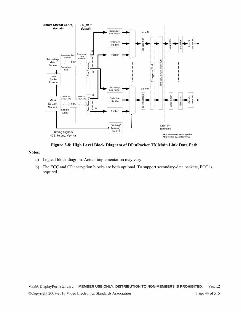
VESA DisplayPort Standard MEMBER USE ONLY. DISTRIBUTION TO NON-MEMBERS IS PROHIBITED. Ver.1.2
©Copyright 2007-2010 Video Electronics Standards Association Page 44 of 515
Main Stream Source
Stream Data
Timing Signals(DE, Hsync, Vsync)
Secondary-data
SourceSecondary
-data
Native Stream CLK(s)domain
Bus
Ste
erin
g
Packer
Framing/Mux-ing Control
Delimiter/Stuffer
LS_CLKdomain
Scr
ambl
er
Enc
oder
P-to
-S
conv
erte
r
Secondary-data Packer
Packer
Delimiter/Stuffer
Scr
ambl
er
Enc
oder
P-to
-S
conv
erte
r
Secondary-data Packer
TBC
TBC
Bus
Ste
erin
g
8
8
8
8
16/18/20/24/30/…/48
Lane N
Lane 0
Link/PHY Boundary
Secondary-data
data unit
Secondary-data data unit
Info Packet
Encoder
16/18/20/24/30/…/48
SR = Scrambler Reset symbolTBC = Time Base Converter
Encr
yptio
n Bl
ock
SR
Inse
rtion
SR
Inse
rtion
Inte
rlane
Ske
w In
serti
on
Figure 2-8: High Level Block Diagram of DP uPacket TX Main Link Data Path
Notes:
a) Logical block diagram. Actual implementation may vary.
b) The ECC and CP encryption blocks are both optional. To support secondary-data packets, ECC is required.
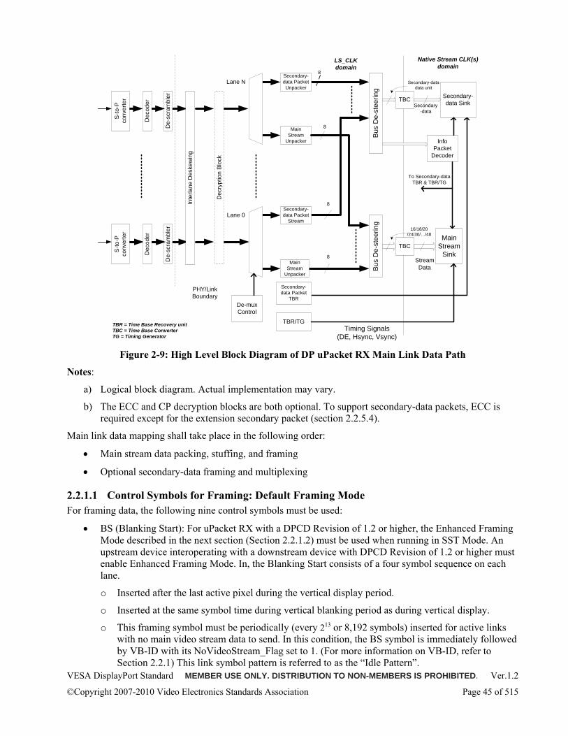
VESA DisplayPort Standard MEMBER USE ONLY. DISTRIBUTION TO NON-MEMBERS IS PROHIBITED. Ver.1.2
©Copyright 2007-2010 Video Electronics Standards Association Page 45 of 515
Main Stream
Sink
Timing Signals(DE, Hsync, Vsync)
Secondary-data SinkSecondary
-data
Native Stream CLK(s)domain
Main Stream
Unpacker
De-mux Control
LS_CLKdomain
De-
scra
mbl
er
S-to
-P
conv
erte
rMain
Stream Unpacker
De-
scra
mbl
er
S-to
-P
conv
erte
r
Secondary-data Packet Unpacker
TBR/TG
Secondary-data Packet
TBR
TBC
Bus
De-
stee
ring
TBC
8
8
8
8
Bus
De-
stee
ring
StreamData
16/18/20/24/30/…/48
Lane N
Lane 0
Secondary-data data unit
PHY/Link Boundary
InfoPacket
Decoder
To Secondary-data TBR & TBR/TG
TBR = Time Base Recovery unitTBC = Time Base ConverterTG = Timing Generator
Inte
rlane
Des
kew
ing
Dec
oder
Dec
oder
Dec
rypt
ion
Blo
ck
Secondary-data Packet
Stream
Figure 2-9: High Level Block Diagram of DP uPacket RX Main Link Data Path
Notes:
a) Logical block diagram. Actual implementation may vary.
b) The ECC and CP decryption blocks are both optional. To support secondary-data packets, ECC is required except for the extension secondary packet (section 2.2.5.4).
Main link data mapping shall take place in the following order:
• Main stream data packing, stuffing, and framing
• Optional secondary-data framing and multiplexing
2.2.1.1 Control Symbols for Framing: Default Framing Mode For framing data, the following nine control symbols must be used:
• BS (Blanking Start): For uPacket RX with a DPCD Revision of 1.2 or higher, the Enhanced Framing Mode described in the next section (Section 2.2.1.2) must be used when running in SST Mode. An upstream device interoperating with a downstream device with DPCD Revision of 1.2 or higher must enable Enhanced Framing Mode. In, the Blanking Start consists of a four symbol sequence on each lane.
o Inserted after the last active pixel during the vertical display period.
o Inserted at the same symbol time during vertical blanking period as during vertical display.
o This framing symbol must be periodically (every 213 or 8,192 symbols) inserted for active links with no main video stream data to send. In this condition, the BS symbol is immediately followed by VB-ID with its NoVideoStream_Flag set to 1. (For more information on VB-ID, refer to Section 2.2.1) This link symbol pattern is referred to as the “Idle Pattern”.
VESA DisplayPort Standard MEMBER USE ONLY. DISTRIBUTION TO NON-MEMBERS IS PROHIBITED. Ver.1.2
©Copyright 2007-2010 Video Electronics Standards Association Page 46 of 515
• BE (Blanking End)
o Inserted immediately before the first active pixel of a line only during the vertical display period
• FS (Fill Start)
o Inserted at the beginning of stuffing symbols in the transfer unit. Note: Transfer unit is described in Section 2.2.1.4.1.
o Omitted when there is only one stuffing symbol. In this case, FE (Fill End) is inserted without FS.
o FS and FE are inserted with no stuffing data symbols in between when there are only two stuffing symbols.
• FE (Fill End)
o Inserted at the end of stuffing symbols within transfer unit.
• SS (Secondary-data Start)
o Inserted at the beginning of secondary-data
• SE (Secondary-data End)
o Inserted at the end of the secondary-data
• SR (Scrambler Reset): For uPacket RX with a DPCD Revision of 1.2 or higher, the Enhanced Framing Mode described in the next section (Section 2.2.1.2) must be used when running in SST Mode. An upstream device interoperating with a downstream device whose DPCD Revision is 1.2 or higher must enable Enhanced Framing Mode. In Enhanced Framing Mode, the Scrambler Reset consists of four symbol sequence on each lane.
o Every 512th BS symbol must be replaced with a SR symbol by a uPacket TX to reset the LFSR of the scrambler.
• CPBS (Content Protection BS): For uPacket RX with a DPCD Revision of 1.2 or higher, the Enhanced Framing Mode described in the next section (Section 2.2.1.2) must be used when running in SST Mode. An upstream device interoperating with a downstream device whose DPCD Revision is 1.2 or higher must enable Enhanced Framing Mode. In Enhanced Framing Mode, the Content Protection BS consists of 4 symbol sequence on each lane.
o Used by a CP system. Called “CP” symbol in the Enhanced Framing Mode described in Section 2.2.1.2.
• CPSR (Content Protection SR): For uPacket RX with a DPCD Revision of 1.2 or higher, the Enhanced Framing Mode described in the next section (Section 2.2.1.2) must be used when running in SST Mode. An upstream device interoperating with a downstream device whose DPCD Revision is 1.2 or higher must enable Enhanced Framing Mode. In Enhanced Framing Mode, the Content Protection SR consists of 4 symbol sequence on each lane.
o Used by a CP system. CPSR resets the LFSR of the scrambler just as SR does. Called “BF” symbol in the Enhanced Framing Mode described in Section 2.2.1.2.
These control symbols must be inserted in all lanes in the same LS_Clk cycle (before they get inter-lane skewed by 2 LS_Clk cycles just before going to the PHY Layer). The link layer must distinguish these control symbols from data symbols so that the physical layer can properly encode these control symbols using “special characters”.
For example, the link layer may use the 9th bit to indicate whether the accompanying 8-bit data represents control symbols or data symbols. There are many ways for the link layer to implement this distinction, the method used is implementation-specific and beyond the scope of this document.
VESA DisplayPort Standard MEMBER USE ONLY. DISTRIBUTION TO NON-MEMBERS IS PROHIBITED. Ver.1.2
©Copyright 2007-2010 Video Electronics Standards Association Page 47 of 515
2.2.1.2 Control Symbols for Framing: Enhanced Framing Mode BS, SR, CPBS, and CPSR symbols must be replaced as shown in Table 2-61: in enhanced mode. The enhanced framing mode is enabled only when both DisplayPort uPacket and uPacket RX support it.
A DisplayPort uPacket RX indicates its support with ENHANCED_FRAME_CAP bit in the uPacket RX capability field of DPCD (bit 7 of address 2h). A DisplayPort uPacket TX enables it by writing 1 to ENHANCED_FRAME_EN bit in the link configuration field of DPCD (bit 7 of address 101h) as described in Table 2-75. Once enabled, BS, SR, CPBS, and CPSR symbols must be replaced with the four symbol sequence in Table 2-61: regardless of the lane count of the main link.
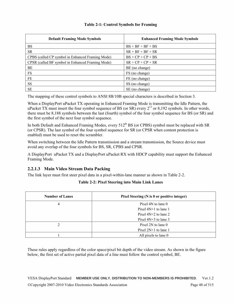
VESA DisplayPort Standard MEMBER USE ONLY. DISTRIBUTION TO NON-MEMBERS IS PROHIBITED. Ver.1.2
©Copyright 2007-2010 Video Electronics Standards Association Page 48 of 515
Table 2-1: Control Symbols for Framing
Default Framing Mode Symbols Enhanced Framing Mode Symbols
BS BS + BF + BF + BS SR SR + BF + BF + SR CPBS (called CP symbol in Enhanced Framing Mode) BS + CP + CP + BS CPSR (called BF symbol in Enhanced Framing Mode) SR + CP + CP + SR BE BE (no change) FS FS (no change) FE FE (no change) SS SS (no change) SE SE (no change)
The mapping of these control symbols to ANSI 8B/10B special characters is described in Section 3.
When a DisplayPort uPacket TX operating in Enhanced Framing Mode is transmitting the Idle Pattern, the uPacket TX must insert the four symbol sequence of BS (or SR) every 213 or 8,192 symbols. In other words, there must be 8,188 symbols between the last (fourth) symbol of the four symbol sequence for BS (or SR) and the first symbol of the next four symbol sequence.
In both Default and Enhanced Framing Modes, every 512th BS (or CPBS) symbol must be replaced with SR (or CPSR). The last symbol of the four symbol sequence for SR (or CPSR when content protection is enabled) must be used to reset the scrambler.
When switching between the Idle Pattern transmission and a stream transmission, the Source device must avoid any overlap of the four symbols for BS, SR, CPBS and CPSR.
A DisplayPort uPacket TX and a DisplayPort uPacket RX with HDCP capability must support the Enhanced Framing Mode.
2.2.1.3 Main Video Stream Data Packing The link layer must first steer pixel data in a pixel-within-lane manner as shown in Table 2-2.
Table 2-2: Pixel Steering into Main Link Lanes
Number of Lanes Pixel Steering (N is 0 or positive integer)
4 Pixel 4N to lane 0 Pixel 4N+1 to lane 1 Pixel 4N+2 to lane 2 Pixel 4N+3 to lane 3
2 Pixel 2N to lane 0 Pixel 2N+1 to lane 1
1 All pixels to lane 0
These rules apply regardless of the color space/pixel bit depth of the video stream. As shown in the figure below, the first set of active partial pixel data of a line must follow the control symbol, BE.
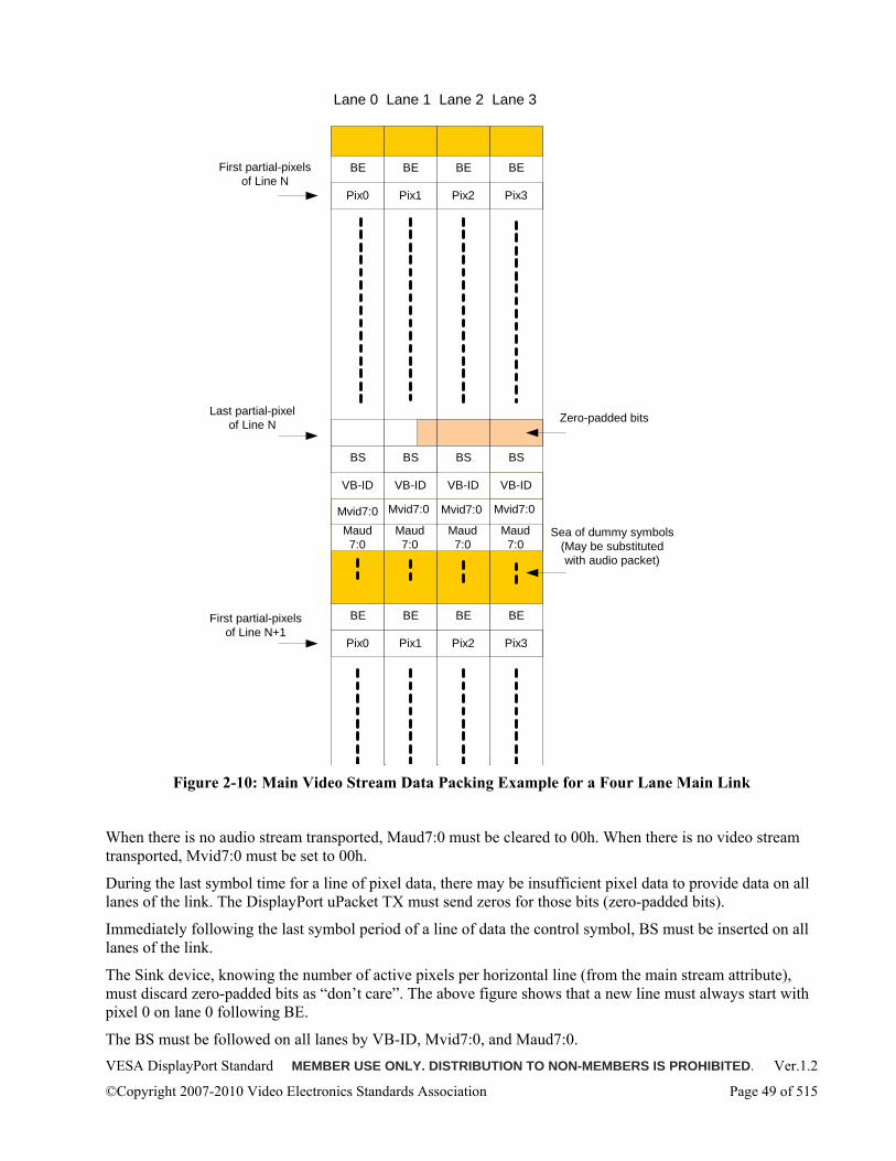
VESA DisplayPort Standard MEMBER USE ONLY. DISTRIBUTION TO NON-MEMBERS IS PROHIBITED. Ver.1.2
©Copyright 2007-2010 Video Electronics Standards Association Page 49 of 515
BS
First partial-pixelsof Line N
Last partial-pixelof Line N Zero-padded bits
Pix0 Pix1 Pix2 Pix3
BSPix0 Pix1 Pix2 Pix3
Sea of dummy symbols(May be substitutedwith audio packet)
First partial-pixelsof Line N+1
VB-IDVB-IDVB-ID VB-ID
Mvid7:0
Lane 0 Lane 1 Lane 2 Lane 3
Mvid7:0 Mvid7:0 Mvid7:0
Maud7:0
BS BS BS BS
BE BE BE BE
BE BE BE BE
Maud7:0
Maud7:0
Maud7:0
Figure 2-10: Main Video Stream Data Packing Example for a Four Lane Main Link
When there is no audio stream transported, Maud7:0 must be cleared to 00h. When there is no video stream transported, Mvid7:0 must be set to 00h.
During the last symbol time for a line of pixel data, there may be insufficient pixel data to provide data on all lanes of the link. The DisplayPort uPacket TX must send zeros for those bits (zero-padded bits).
Immediately following the last symbol period of a line of data the control symbol, BS must be inserted on all lanes of the link.
The Sink device, knowing the number of active pixels per horizontal line (from the main stream attribute), must discard zero-padded bits as “don’t care”. The above figure shows that a new line must always start with pixel 0 on lane 0 following BE.
The BS must be followed on all lanes by VB-ID, Mvid7:0, and Maud7:0.
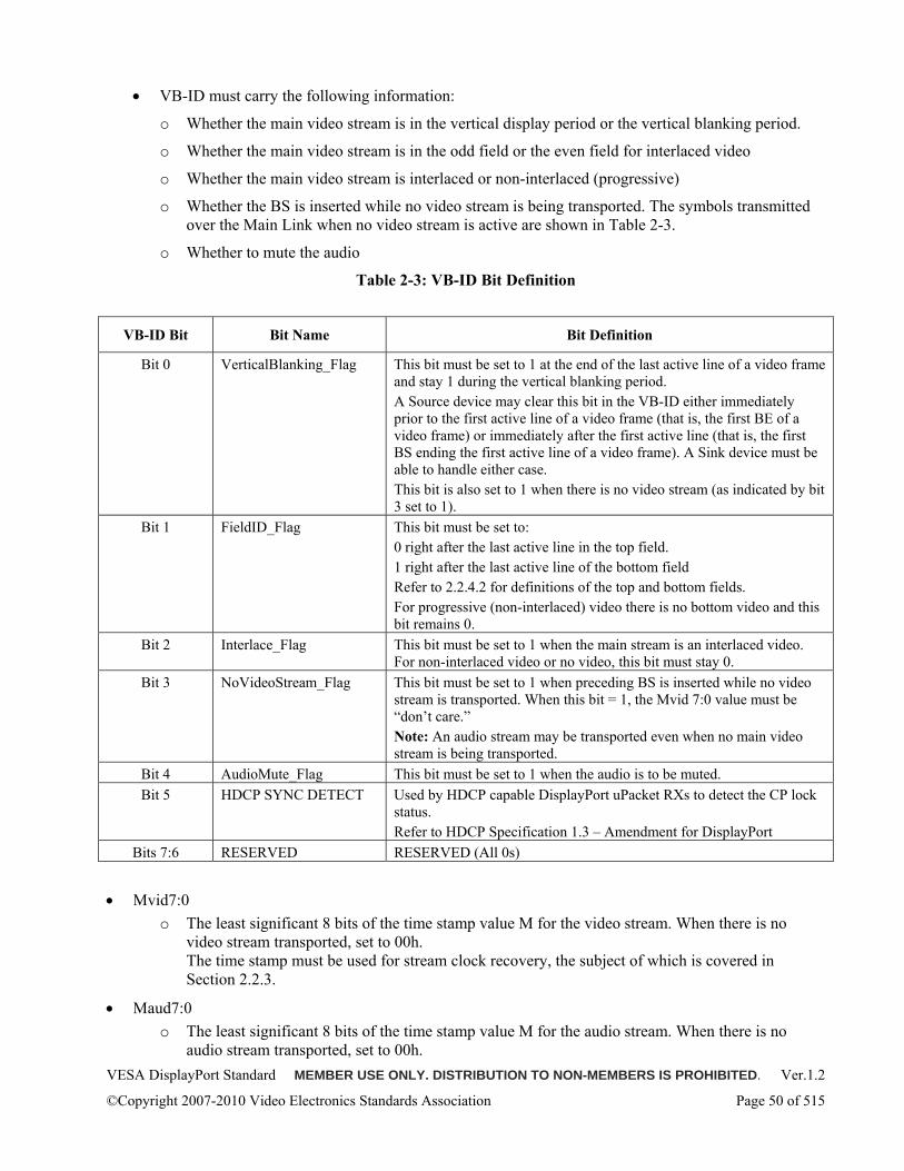
VESA DisplayPort Standard MEMBER USE ONLY. DISTRIBUTION TO NON-MEMBERS IS PROHIBITED. Ver.1.2
©Copyright 2007-2010 Video Electronics Standards Association Page 50 of 515
• VB-ID must carry the following information:
o Whether the main video stream is in the vertical display period or the vertical blanking period.
o Whether the main video stream is in the odd field or the even field for interlaced video
o Whether the main video stream is interlaced or non-interlaced (progressive)
o Whether the BS is inserted while no video stream is being transported. The symbols transmitted over the Main Link when no video stream is active are shown in Table 2-3.
o Whether to mute the audio
Table 2-3: VB-ID Bit Definition
VB-ID Bit Bit Name Bit Definition
Bit 0 VerticalBlanking_Flag This bit must be set to 1 at the end of the last active line of a video frame and stay 1 during the vertical blanking period. A Source device may clear this bit in the VB-ID either immediately prior to the first active line of a video frame (that is, the first BE of a video frame) or immediately after the first active line (that is, the first BS ending the first active line of a video frame). A Sink device must be able to handle either case. This bit is also set to 1 when there is no video stream (as indicated by bit 3 set to 1).
Bit 1 FieldID_Flag This bit must be set to: 0 right after the last active line in the top field. 1 right after the last active line of the bottom field Refer to 2.2.4.2 for definitions of the top and bottom fields. For progressive (non-interlaced) video there is no bottom video and this bit remains 0.
Bit 2 Interlace_Flag This bit must be set to 1 when the main stream is an interlaced video. For non-interlaced video or no video, this bit must stay 0.
Bit 3 NoVideoStream_Flag This bit must be set to 1 when preceding BS is inserted while no video stream is transported. When this bit = 1, the Mvid 7:0 value must be “don’t care.” Note: An audio stream may be transported even when no main video stream is being transported.
Bit 4 AudioMute_Flag This bit must be set to 1 when the audio is to be muted. Bit 5 HDCP SYNC DETECT Used by HDCP capable DisplayPort uPacket RXs to detect the CP lock
status. Refer to HDCP Specification 1.3 – Amendment for DisplayPort
Bits 7:6 RESERVED RESERVED (All 0s)
• Mvid7:0 o The least significant 8 bits of the time stamp value M for the video stream. When there is no
video stream transported, set to 00h. The time stamp must be used for stream clock recovery, the subject of which is covered in Section 2.2.3.
• Maud7:0 o The least significant 8 bits of the time stamp value M for the audio stream. When there is no
audio stream transported, set to 00h.
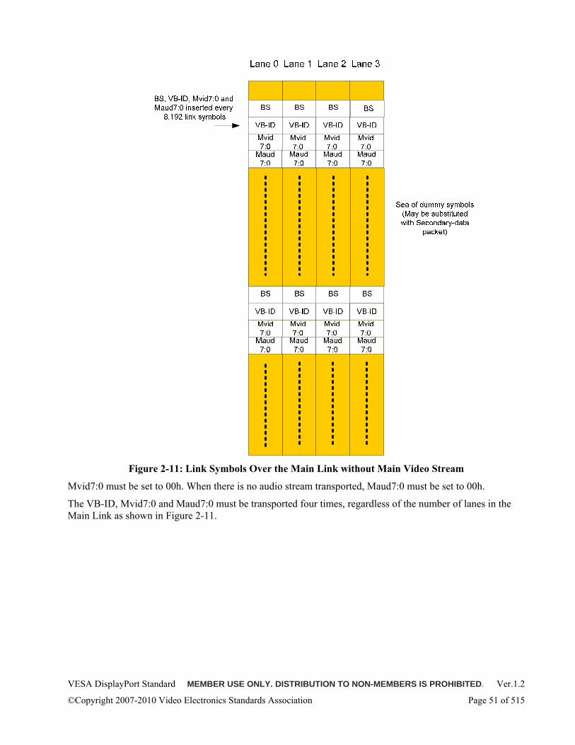
VESA DisplayPort Standard MEMBER USE ONLY. DISTRIBUTION TO NON-MEMBERS IS PROHIBITED. Ver.1.2
©Copyright 2007-2010 Video Electronics Standards Association Page 51 of 515
Figure 2-11: Link Symbols Over the Main Link without Main Video Stream
Mvid7:0 must be set to 00h. When there is no audio stream transported, Maud7:0 must be set to 00h.
The VB-ID, Mvid7:0 and Maud7:0 must be transported four times, regardless of the number of lanes in the Main Link as shown in Figure 2-11.
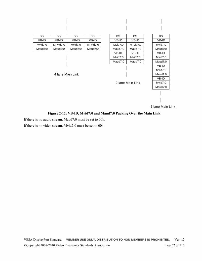
VESA DisplayPort Standard MEMBER USE ONLY. DISTRIBUTION TO NON-MEMBERS IS PROHIBITED. Ver.1.2
©Copyright 2007-2010 Video Electronics Standards Association Page 52 of 515
BSVB-ID
Mvid7:0
VB-IDMvid7:0
VB-IDMvid7:0
VB-IDMvid7:0
Maud7:0
Maud7:0
Maud7:0
Maud7:0
1 lane Main Link
BSVB-ID
Mvid7:0
VB-IDMvid7:0
BSVB-ID
M_vid7:0
VB-IDMvid7:0
Maud7:0 Maud7:0
Maud7:0 Maud7:0
2 lane Main Link
BSVB-ID
Mvid7:0
BSVB-ID
M_vid7:0Maud7:0 Maud7:0
BSVB-ID
Mvid7:0
BSVB-ID
M_vid7:0Maud7:0 Maud7:0
4 lane Main Link
Figure 2-12: VB-ID, Mvid7:0 and Maud7:0 Packing Over the Main Link
If there is no audio stream, Maud7:0 must be set to 00h.
If there is no video stream, Mvid7:0 must be set to 00h.
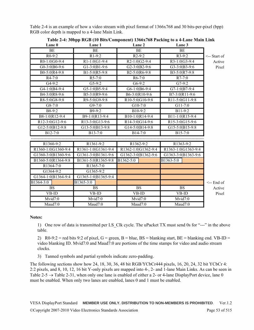
VESA DisplayPort Standard MEMBER USE ONLY. DISTRIBUTION TO NON-MEMBERS IS PROHIBITED. Ver.1.2
©Copyright 2007-2010 Video Electronics Standards Association Page 53 of 515
Table 2-4 is an example of how a video stream with pixel format of 1366x768 and 30 bits-per-pixel (bpp) RGB color depth is mapped to a 4-lane Main Link.
Table 2-4: 30bpp RGB (10 Bits/Component) 1366x768 Packing to a 4-Lane Main Link Lane 0 Lane 1 Lane 2 Lane 3
BE BE BE BER0-9:2 R1-9:2 R2-9:2 R3-9:2 <-- Start of
R0-1:0|G0-9:4 R1-1:0|G1-9:4 R2-1:0|G2-9:4 R3-1:0|G3-9:4 ActiveG0-3:0|B0-9:6 G1-3:0|B1-9:6 G2-3:0|B2-9:6 G3-3:0|B3-9:6 PixelB0-5:0|R4-9:8 B1-5:0|R5-9:8 B2-5:0|R6-9:8 B3-5:0|R7-9:8
R4-7:0 R5-7:0 R6-7:0 R7-7:0G4-9:2 G5-9:2 G6-9:2 G7-9:2
G4-1:0|B4-9:4 G5-1:0|B5-9:4 G6-1:0|B6-9:4 G7-1:0|B7-9:4B4-3:0|R8-9:6 B5-3:0|R9-9:6 B6-3:0|R10-9:6 B7-3:0|R11-9:6R8-5:0|G8-9:8 R9-5:0|G9-9:8 R10-5:0|G10-9:8 R11-5:0|G11-9:8
G8-7:0 G9-7:0 G10-7:0 G11-7:0B8-9:2 B9-9:2 B10-9:2 B11-9:2
B8-1:0|R12-9:4 B9-1:0|R13-9:4 B10-1:0|R14-9:4 B11-1:0|R15-9:4R12-3:0|G12-9:6 R13-3:0|G13-9:6 R14-3:0|G14-9:6 R15-3:0|G15-9:6G12-5:0|B12-9:8 G13-5:0|B13-9:8 G14-5:0|B14-9:8 G15-5:0|B15-9:8
B12-7:0 B13-7:0 B14-7:0 B15-7:0
R1360-9:2 R1361-9:2 R1362-9:2 R1363-9:2R1360-1:0|G1360-9:4 R1361-1:0|G1361-9:4 R1362-1:0|G1362-9:4 R1363-1:0|G1363-9:4G1360-3:0|B1360-9:6 G1361-3:0|B1361-9:6 G1362-3:0|B1362-9:6 G1363-3:0|B1363-9:6B1360-5:0|R1364-9:8 B1361-5:0|R1365-9:8 B1362-5:0 B1363-5:0
R1364-7:0 R1365-7:0G1364-9:2 G1365-9:2
G1364-1:0|B1364-9:4 G1365-1:0|B1365-9:4B1364-3:0 B1365-3:0 <-- End of
BS BS BS BS ActiveVB-ID VB-ID VB-ID VB-ID Pixel
Mvid7:0 Mvid7:0 Mvid7:0 Mvid7:0Maud7:0 Maud7:0 Maud7:0 Maud7:0
----------------------------------------------------------------------------------------------------------------------------
Notes:
1) One row of data is transmitted per LS_Clk cycle. The uPacket TX must send 0s for “---” in the above table.
2) R0-9:2 = red bits 9:2 of pixel, G = green, B = blue, BS = blanking start, BE = blanking end. VB-ID = video blanking ID. Mvid7:0 and Maud7:0 are portions of the time stamps for video and audio stream clocks.
3) Tanned symbols and partial symbols indicate zero-padding.
The following sections show how 24, 18, 30, 36, 48 bit RGB/YCbCr444 pixels, 16, 20, 24, 32 bit YCbCr 4: 2:2 pixels, and 8, 10, 12, 16 bit Y-only pixels are mapped into 4-, 2- and 1-lane Main Links. As can be seen in Table 2-5 → Table 2-31, when only one lane is enabled of either a 2- or 4-lane DisplayPort device, lane 0 must be enabled. When only two lanes are enabled, lanes 0 and 1 must be enabled.
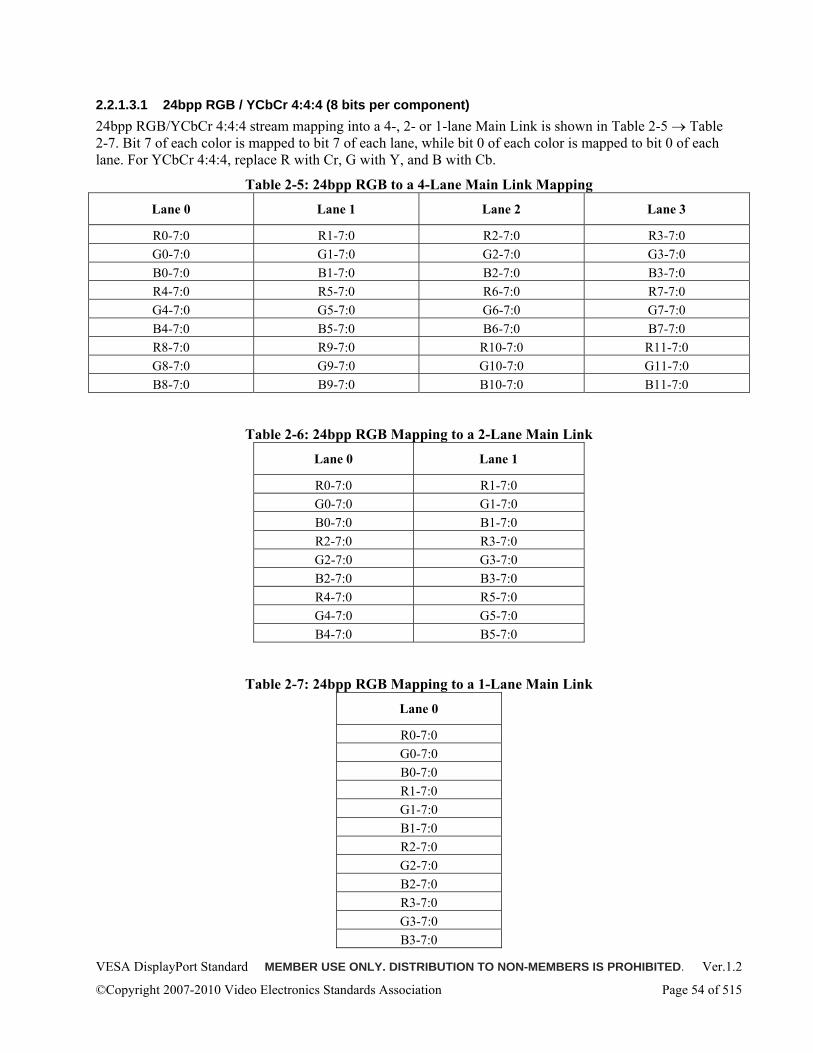
VESA DisplayPort Standard MEMBER USE ONLY. DISTRIBUTION TO NON-MEMBERS IS PROHIBITED. Ver.1.2
©Copyright 2007-2010 Video Electronics Standards Association Page 54 of 515
2.2.1.3.1 24bpp RGB / YCbCr 4:4:4 (8 bits per component) 24bpp RGB/YCbCr 4:4:4 stream mapping into a 4-, 2- or 1-lane Main Link is shown in Table 2-5 → Table 2-7. Bit 7 of each color is mapped to bit 7 of each lane, while bit 0 of each color is mapped to bit 0 of each lane. For YCbCr 4:4:4, replace R with Cr, G with Y, and B with Cb.
Table 2-5: 24bpp RGB to a 4-Lane Main Link Mapping
Lane 0 Lane 1 Lane 2 Lane 3
R0-7:0 R1-7:0 R2-7:0 R3-7:0 G0-7:0 G1-7:0 G2-7:0 G3-7:0 B0-7:0 B1-7:0 B2-7:0 B3-7:0 R4-7:0 R5-7:0 R6-7:0 R7-7:0 G4-7:0 G5-7:0 G6-7:0 G7-7:0 B4-7:0 B5-7:0 B6-7:0 B7-7:0 R8-7:0 R9-7:0 R10-7:0 R11-7:0 G8-7:0 G9-7:0 G10-7:0 G11-7:0 B8-7:0 B9-7:0 B10-7:0 B11-7:0
Table 2-6: 24bpp RGB Mapping to a 2-Lane Main Link
Lane 0 Lane 1
R0-7:0 R1-7:0 G0-7:0 G1-7:0 B0-7:0 B1-7:0 R2-7:0 R3-7:0 G2-7:0 G3-7:0 B2-7:0 B3-7:0 R4-7:0 R5-7:0 G4-7:0 G5-7:0 B4-7:0 B5-7:0
Table 2-7: 24bpp RGB Mapping to a 1-Lane Main Link
Lane 0
R0-7:0 G0-7:0 B0-7:0 R1-7:0 G1-7:0 B1-7:0 R2-7:0 G2-7:0 B2-7:0 R3-7:0 G3-7:0 B3-7:0
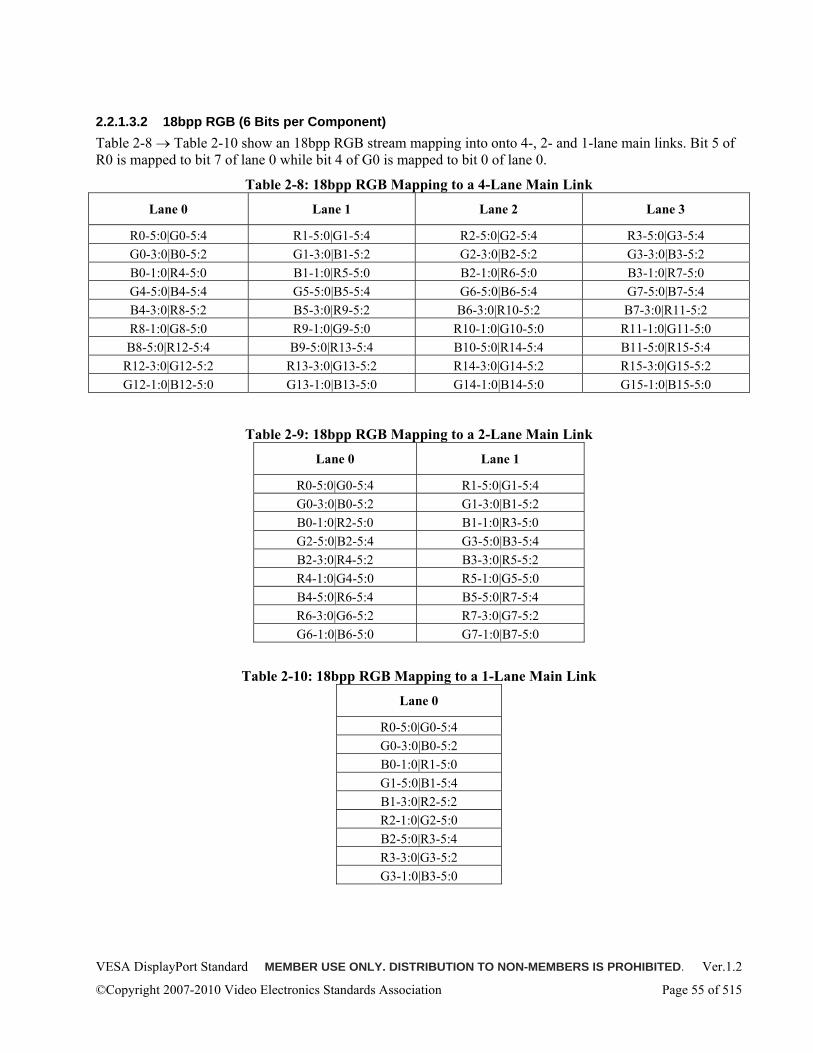
VESA DisplayPort Standard MEMBER USE ONLY. DISTRIBUTION TO NON-MEMBERS IS PROHIBITED. Ver.1.2
©Copyright 2007-2010 Video Electronics Standards Association Page 55 of 515
2.2.1.3.2 18bpp RGB (6 Bits per Component) Table 2-8 → Table 2-10 show an 18bpp RGB stream mapping into onto 4-, 2- and 1-lane main links. Bit 5 of R0 is mapped to bit 7 of lane 0 while bit 4 of G0 is mapped to bit 0 of lane 0.
Table 2-8: 18bpp RGB Mapping to a 4-Lane Main Link
Lane 0 Lane 1 Lane 2 Lane 3
R0-5:0|G0-5:4 R1-5:0|G1-5:4 R2-5:0|G2-5:4 R3-5:0|G3-5:4 G0-3:0|B0-5:2 G1-3:0|B1-5:2 G2-3:0|B2-5:2 G3-3:0|B3-5:2 B0-1:0|R4-5:0 B1-1:0|R5-5:0 B2-1:0|R6-5:0 B3-1:0|R7-5:0 G4-5:0|B4-5:4 G5-5:0|B5-5:4 G6-5:0|B6-5:4 G7-5:0|B7-5:4 B4-3:0|R8-5:2 B5-3:0|R9-5:2 B6-3:0|R10-5:2 B7-3:0|R11-5:2 R8-1:0|G8-5:0 R9-1:0|G9-5:0 R10-1:0|G10-5:0 R11-1:0|G11-5:0 B8-5:0|R12-5:4 B9-5:0|R13-5:4 B10-5:0|R14-5:4 B11-5:0|R15-5:4
R12-3:0|G12-5:2 R13-3:0|G13-5:2 R14-3:0|G14-5:2 R15-3:0|G15-5:2 G12-1:0|B12-5:0 G13-1:0|B13-5:0 G14-1:0|B14-5:0 G15-1:0|B15-5:0
Table 2-9: 18bpp RGB Mapping to a 2-Lane Main Link
Lane 0 Lane 1
R0-5:0|G0-5:4 R1-5:0|G1-5:4 G0-3:0|B0-5:2 G1-3:0|B1-5:2 B0-1:0|R2-5:0 B1-1:0|R3-5:0 G2-5:0|B2-5:4 G3-5:0|B3-5:4 B2-3:0|R4-5:2 B3-3:0|R5-5:2 R4-1:0|G4-5:0 R5-1:0|G5-5:0 B4-5:0|R6-5:4 B5-5:0|R7-5:4 R6-3:0|G6-5:2 R7-3:0|G7-5:2 G6-1:0|B6-5:0 G7-1:0|B7-5:0
Table 2-10: 18bpp RGB Mapping to a 1-Lane Main Link
Lane 0
R0-5:0|G0-5:4 G0-3:0|B0-5:2 B0-1:0|R1-5:0 G1-5:0|B1-5:4 B1-3:0|R2-5:2 R2-1:0|G2-5:0 B2-5:0|R3-5:4 R3-3:0|G3-5:2 G3-1:0|B3-5:0
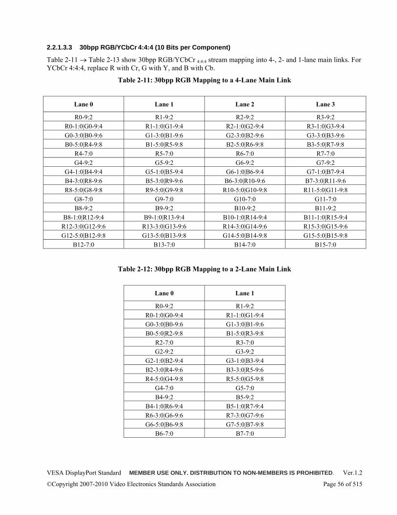
VESA DisplayPort Standard MEMBER USE ONLY. DISTRIBUTION TO NON-MEMBERS IS PROHIBITED. Ver.1.2
©Copyright 2007-2010 Video Electronics Standards Association Page 56 of 515
2.2.1.3.3 30bpp RGB/YCbCr 4:4:4 (10 Bits per Component)
Table 2-11 → Table 2-13 show 30bpp RGB/YCbCr 4:4:4 stream mapping into 4-, 2- and 1-lane main links. For YCbCr 4:4:4, replace R with Cr, G with Y, and B with Cb.
Table 2-11: 30bpp RGB Mapping to a 4-Lane Main Link
Lane 0 Lane 1 Lane 2 Lane 3
R0-9:2 R1-9:2 R2-9:2 R3-9:2 R0-1:0|G0-9:4 R1-1:0|G1-9:4 R2-1:0|G2-9:4 R3-1:0|G3-9:4 G0-3:0|B0-9:6 G1-3:0|B1-9:6 G2-3:0|B2-9:6 G3-3:0|B3-9:6 B0-5:0|R4-9:8 B1-5:0|R5-9:8 B2-5:0|R6-9:8 B3-5:0|R7-9:8
R4-7:0 R5-7:0 R6-7:0 R7-7:0 G4-9:2 G5-9:2 G6-9:2 G7-9:2
G4-1:0|B4-9:4 G5-1:0|B5-9:4 G6-1:0|B6-9:4 G7-1:0|B7-9:4 B4-3:0|R8-9:6 B5-3:0|R9-9:6 B6-3:0|R10-9:6 B7-3:0|R11-9:6 R8-5:0|G8-9:8 R9-5:0|G9-9:8 R10-5:0|G10-9:8 R11-5:0|G11-9:8
G8-7:0 G9-7:0 G10-7:0 G11-7:0 B8-9:2 B9-9:2 B10-9:2 B11-9:2
B8-1:0|R12-9:4 B9-1:0|R13-9:4 B10-1:0|R14-9:4 B11-1:0|R15-9:4 R12-3:0|G12-9:6 R13-3:0|G13-9:6 R14-3:0|G14-9:6 R15-3:0|G15-9:6 G12-5:0|B12-9:8 G13-5:0|B13-9:8 G14-5:0|B14-9:8 G15-5:0|B15-9:8
B12-7:0 B13-7:0 B14-7:0 B15-7:0
Table 2-12: 30bpp RGB Mapping to a 2-Lane Main Link
Lane 0 Lane 1
R0-9:2 R1-9:2 R0-1:0|G0-9:4 R1-1:0|G1-9:4 G0-3:0|B0-9:6 G1-3:0|B1-9:6 B0-5:0|R2-9:8 B1-5:0|R3-9:8
R2-7:0 R3-7:0 G2-9:2 G3-9:2
G2-1:0|B2-9:4 G3-1:0|B3-9:4 B2-3:0|R4-9:6 B3-3:0|R5-9:6 R4-5:0|G4-9:8 R5-5:0|G5-9:8
G4-7:0 G5-7:0 B4-9:2 B5-9:2
B4-1:0|R6-9:4 B5-1:0|R7-9:4 R6-3:0|G6-9:6 R7-3:0|G7-9:6 G6-5:0|B6-9:8 G7-5:0|B7-9:8
B6-7:0 B7-7:0
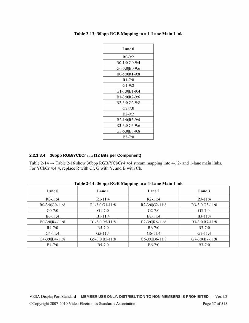
VESA DisplayPort Standard MEMBER USE ONLY. DISTRIBUTION TO NON-MEMBERS IS PROHIBITED. Ver.1.2
©Copyright 2007-2010 Video Electronics Standards Association Page 57 of 515
Table 2-13: 30bpp RGB Mapping to a 1-Lane Main Link
Lane 0
R0-9:2 R0-1:0|G0-9:4 G0-3:0|B0-9:6 B0-5:0|R1-9:8
R1-7:0 G1-9:2
G1-1:0|B1-9:4 B1-3:0|R2-9:6 R2-5:0|G2-9:8
G2-7:0 B2-9:2
B2-1:0|R3-9:4 R3-3:0|G3-9:6 G3-5:0|B3-9:8
B3-7:0
2.2.1.3.4 36bpp RGB/YCbCr 4:4:4 (12 Bits per Component)
Table 2-14 → Table 2-16 show 36bpp RGB/YCbCr 4:4:4 stream mapping into 4-, 2- and 1-lane main links. For YCbCr 4:4:4, replace R with Cr, G with Y, and B with Cb.
Table 2-14: 36bpp RGB Mapping to a 4-Lane Main Link
Lane 0 Lane 1 Lane 2 Lane 3
R0-11:4 R1-11:4 R2-11:4 R3-11:4 R0-3:0|G0-11:8 R1-3:0|G1-11:8 R2-3:0|G2-11:8 R3-3:0|G3-11:8
G0-7:0 G1-7:0 G2-7:0 G3-7:0| B0-11:4 B1-11:4 B2-11:4 B3-11:4
B0-3:0|R4-11:8 B1-3:0|R5-11:8 B2-3:0|R6-11:8 B3-3:0|R7-11:8 R4-7:0 R5-7:0 R6-7:0 R7-7:0
G4-11:4 G5-11:4 G6-11:4 G7-11:4 G4-3:0|B4-11:8 G5-3:0|B5-11:8 G6-3:0|B6-11:8 G7-3:0|B7-11:8
B4-7:0 B5-7:0 B6-7:0 B7-7:0
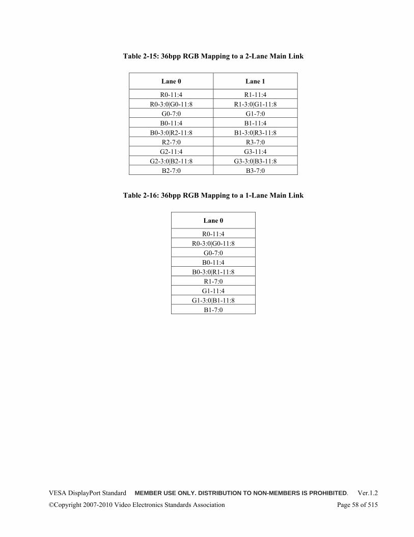
VESA DisplayPort Standard MEMBER USE ONLY. DISTRIBUTION TO NON-MEMBERS IS PROHIBITED. Ver.1.2
©Copyright 2007-2010 Video Electronics Standards Association Page 58 of 515
Table 2-15: 36bpp RGB Mapping to a 2-Lane Main Link
Lane 0 Lane 1
R0-11:4 R1-11:4 R0-3:0|G0-11:8 R1-3:0|G1-11:8
G0-7:0 G1-7:0 B0-11:4 B1-11:4
B0-3:0|R2-11:8 B1-3:0|R3-11:8 R2-7:0 R3-7:0
G2-11:4 G3-11:4 G2-3:0|B2-11:8 G3-3:0|B3-11:8
B2-7:0 B3-7:0
Table 2-16: 36bpp RGB Mapping to a 1-Lane Main Link
Lane 0
R0-11:4 R0-3:0|G0-11:8
G0-7:0 B0-11:4
B0-3:0|R1-11:8 R1-7:0
G1-11:4 G1-3:0|B1-11:8
B1-7:0
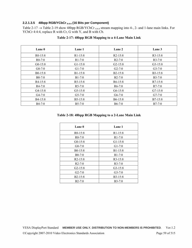
VESA DisplayPort Standard MEMBER USE ONLY. DISTRIBUTION TO NON-MEMBERS IS PROHIBITED. Ver.1.2
©Copyright 2007-2010 Video Electronics Standards Association Page 59 of 515
2.2.1.3.5 48bpp RGB/YCbCr 4:4:4 (16 Bits per Component) Table 2-17 → Table 2-19 show 48bpp RGB/YCbCr 4:4:4 stream mapping into 4-, 2- and 1-lane main links. For YCbCr 4:4:4, replace R with Cr, G with Y, and B with Cb.
Table 2-17: 48bpp RGB Mapping to a 4-Lane Main Link
Lane 0 Lane 1 Lane 2 Lane 3
R0-15:8 R1-15:8 R2-15:8 R3-15:8 R0-7:0 R1-7:0 R2-7:0 R3-7:0
G0-15:8 G1-15:8 G2-15:8 G3-15:8 G0-7:0 G1-7:0 G2-7:0 G3-7:0 B0-15:8 B1-15:8 B2-15:8 B3-15:8 B0-7:0 B1-7:0 B2-7:0 B3-7:0
R4-15:8 R5-15:8 R6-15:8 R7-15:8 R4-7:0 R5-7:0 R6-7:0 R7-7:0
G4-15:8 G5-15:8 G6-15:8 G7-15:8 G4-7:0 G5-7:0 G6-7:0 G7-7:0 B4-15:8 B5-15:8 B6-15:8 B7-15:8 B4-7:0 B5-7:0 B6-7:0 B7-7:0
Table 2-18: 48bpp RGB Mapping to a 2-Lane Main Link
Lane 0 Lane 1
R0-15:8 R1-15:8 R0-7:0 R1-7:0
G0-15:8 G1-15:8 G0-7:0 G1-7:0 B0-15:8 B1-15:8 B0-7:0 B1-7:0
R2-15:8 R3-15:8 R2-7:0 R3-7:0
G2-15:8 G3-15:8 G2-7:0 G3-7:0 B2-15:8 B3-15:8 B2-7:0 B3-7:0
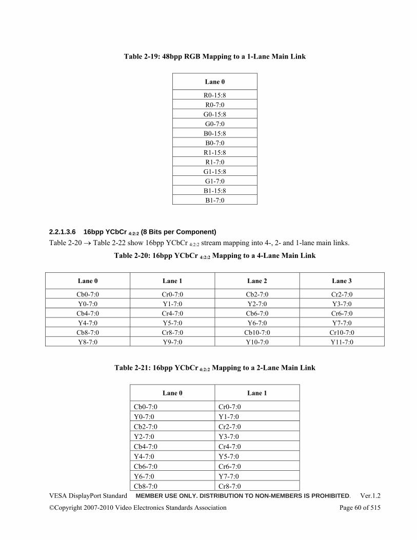
VESA DisplayPort Standard MEMBER USE ONLY. DISTRIBUTION TO NON-MEMBERS IS PROHIBITED. Ver.1.2
©Copyright 2007-2010 Video Electronics Standards Association Page 60 of 515
Table 2-19: 48bpp RGB Mapping to a 1-Lane Main Link
Lane 0
R0-15:8 R0-7:0
G0-15:8 G0-7:0 B0-15:8 B0-7:0
R1-15:8 R1-7:0
G1-15:8 G1-7:0 B1-15:8 B1-7:0
2.2.1.3.6 16bpp YCbCr 4:2:2 (8 Bits per Component) Table 2-20 → Table 2-22 show 16bpp YCbCr 4:2:2 stream mapping into 4-, 2- and 1-lane main links.
Table 2-20: 16bpp YCbCr 4:2:2 Mapping to a 4-Lane Main Link
Lane 0 Lane 1 Lane 2 Lane 3
Cb0-7:0 Cr0-7:0 Cb2-7:0 Cr2-7:0 Y0-7:0 Y1-7:0 Y2-7:0 Y3-7:0 Cb4-7:0 Cr4-7:0 Cb6-7:0 Cr6-7:0 Y4-7:0 Y5-7:0 Y6-7:0 Y7-7:0 Cb8-7:0 Cr8-7:0 Cb10-7:0 Cr10-7:0 Y8-7:0 Y9-7:0 Y10-7:0 Y11-7:0
Table 2-21: 16bpp YCbCr 4:2:2 Mapping to a 2-Lane Main Link
Lane 0 Lane 1
Cb0-7:0 Cr0-7:0 Y0-7:0 Y1-7:0 Cb2-7:0 Cr2-7:0 Y2-7:0 Y3-7:0 Cb4-7:0 Cr4-7:0 Y4-7:0 Y5-7:0 Cb6-7:0 Cr6-7:0 Y6-7:0 Y7-7:0 Cb8-7:0 Cr8-7:0
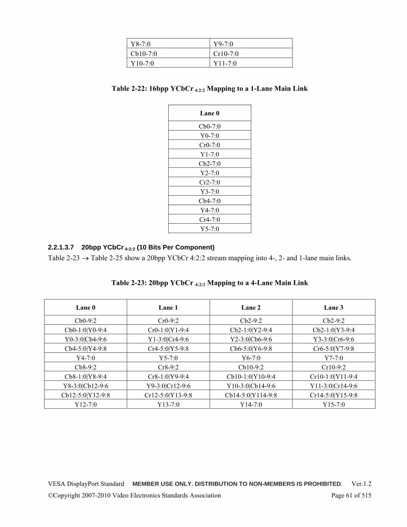
VESA DisplayPort Standard MEMBER USE ONLY. DISTRIBUTION TO NON-MEMBERS IS PROHIBITED. Ver.1.2
©Copyright 2007-2010 Video Electronics Standards Association Page 61 of 515
Y8-7:0 Y9-7:0 Cb10-7:0 Cr10-7:0 Y10-7:0 Y11-7:0
Table 2-22: 16bpp YCbCr 4:2:2 Mapping to a 1-Lane Main Link
Lane 0
Cb0-7:0 Y0-7:0 Cr0-7:0 Y1-7:0 Cb2-7:0 Y2-7:0 Cr2-7:0 Y3-7:0 Cb4-7:0 Y4-7:0 Cr4-7:0 Y5-7:0
2.2.1.3.7 20bpp YCbCr 4:2:2 (10 Bits Per Component) Table 2-23 → Table 2-25 show a 20bpp YCbCr 4:2:2 stream mapping into 4-, 2- and 1-lane main links.
Table 2-23: 20bpp YCbCr 4:2:2 Mapping to a 4-Lane Main Link
Lane 0 Lane 1 Lane 2 Lane 3
Cb0-9:2 Cr0-9:2 Cb2-9:2 Cb2-9:2 Cb0-1:0|Y0-9:4 Cr0-1:0|Y1-9:4 Cb2-1:0|Y2-9:4 Cb2-1:0|Y3-9:4 Y0-3:0|Cb4-9:6 Y1-3:0|Cr4-9:6 Y2-3:0|Cb6-9:6 Y3-3:0|Cr6-9:6 Cb4-5:0|Y4-9:8 Cr4-5:0|Y5-9:8 Cb6-5:0|Y6-9:8 Cr6-5:0|Y7-9:8
Y4-7:0 Y5-7:0 Y6-7:0 Y7-7:0 Cb8-9:2 Cr8-9:2 Cb10-9:2 Cr10-9:2
Cb8-1:0|Y8-9:4 Cr8-1:0|Y9-9:4 Cb10-1:0|Y10-9:4 Cr10-1:0|Y11-9:4 Y8-3:0|Cb12-9:6 Y9-3:0|Cr12-9:6 Y10-3:0|Cb14-9:6 Y11-3:0|Cr14-9:6
Cb12-5:0|Y12-9:8 Cr12-5:0|Y13-9:8 Cb14-5:0|Y114-9:8 Cr14-5:0|Y15-9:8 Y12-7:0 Y13-7:0 Y14-7:0 Y15-7:0
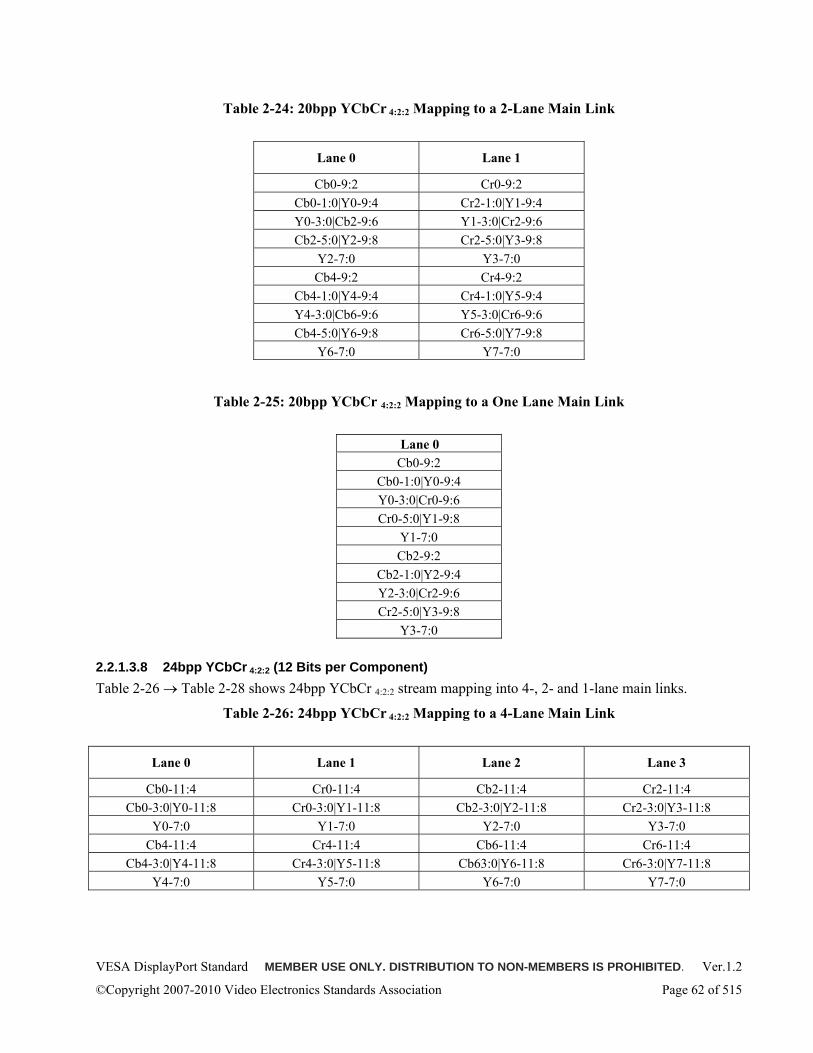
VESA DisplayPort Standard MEMBER USE ONLY. DISTRIBUTION TO NON-MEMBERS IS PROHIBITED. Ver.1.2
©Copyright 2007-2010 Video Electronics Standards Association Page 62 of 515
Table 2-24: 20bpp YCbCr 4:2:2 Mapping to a 2-Lane Main Link
Lane 0 Lane 1
Cb0-9:2 Cr0-9:2 Cb0-1:0|Y0-9:4 Cr2-1:0|Y1-9:4 Y0-3:0|Cb2-9:6 Y1-3:0|Cr2-9:6 Cb2-5:0|Y2-9:8 Cr2-5:0|Y3-9:8
Y2-7:0 Y3-7:0 Cb4-9:2 Cr4-9:2
Cb4-1:0|Y4-9:4 Cr4-1:0|Y5-9:4 Y4-3:0|Cb6-9:6 Y5-3:0|Cr6-9:6 Cb4-5:0|Y6-9:8 Cr6-5:0|Y7-9:8
Y6-7:0 Y7-7:0
Table 2-25: 20bpp YCbCr 4:2:2 Mapping to a One Lane Main Link
Lane 0 Cb0-9:2
Cb0-1:0|Y0-9:4 Y0-3:0|Cr0-9:6 Cr0-5:0|Y1-9:8
Y1-7:0 Cb2-9:2
Cb2-1:0|Y2-9:4 Y2-3:0|Cr2-9:6 Cr2-5:0|Y3-9:8
Y3-7:0
2.2.1.3.8 24bpp YCbCr 4:2:2 (12 Bits per Component) Table 2-26 → Table 2-28 shows 24bpp YCbCr 4:2:2 stream mapping into 4-, 2- and 1-lane main links.
Table 2-26: 24bpp YCbCr 4:2:2 Mapping to a 4-Lane Main Link
Lane 0 Lane 1 Lane 2 Lane 3
Cb0-11:4 Cr0-11:4 Cb2-11:4 Cr2-11:4 Cb0-3:0|Y0-11:8 Cr0-3:0|Y1-11:8 Cb2-3:0|Y2-11:8 Cr2-3:0|Y3-11:8
Y0-7:0 Y1-7:0 Y2-7:0 Y3-7:0 Cb4-11:4 Cr4-11:4 Cb6-11:4 Cr6-11:4
Cb4-3:0|Y4-11:8 Cr4-3:0|Y5-11:8 Cb63:0|Y6-11:8 Cr6-3:0|Y7-11:8 Y4-7:0 Y5-7:0 Y6-7:0 Y7-7:0
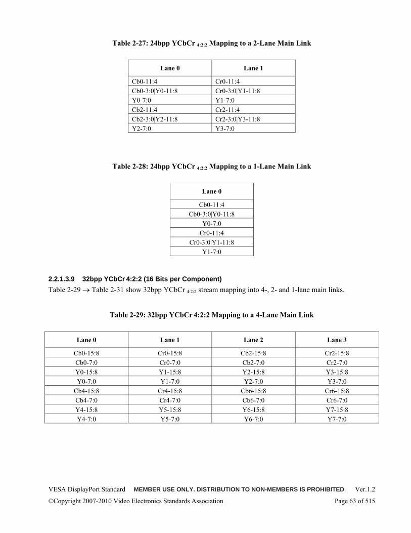
VESA DisplayPort Standard MEMBER USE ONLY. DISTRIBUTION TO NON-MEMBERS IS PROHIBITED. Ver.1.2
©Copyright 2007-2010 Video Electronics Standards Association Page 63 of 515
Table 2-27: 24bpp YCbCr 4:2:2 Mapping to a 2-Lane Main Link
Lane 0 Lane 1
Cb0-11:4 Cr0-11:4 Cb0-3:0|Y0-11:8 Cr0-3:0|Y1-11:8 Y0-7:0 Y1-7:0 Cb2-11:4 Cr2-11:4 Cb2-3:0|Y2-11:8 Cr2-3:0|Y3-11:8 Y2-7:0 Y3-7:0
Table 2-28: 24bpp YCbCr 4:2:2 Mapping to a 1-Lane Main Link
Lane 0
Cb0-11:4 Cb0-3:0|Y0-11:8
Y0-7:0 Cr0-11:4
Cr0-3:0|Y1-11:8 Y1-7:0
2.2.1.3.9 32bpp YCbCr 4:2:2 (16 Bits per Component) Table 2-29 → Table 2-31 show 32bpp YCbCr 4:2:2 stream mapping into 4-, 2- and 1-lane main links.
Table 2-29: 32bpp YCbCr 4:2:2 Mapping to a 4-Lane Main Link
Lane 0 Lane 1 Lane 2 Lane 3
Cb0-15:8 Cr0-15:8 Cb2-15:8 Cr2-15:8 Cb0-7:0 Cr0-7:0 Cb2-7:0 Cr2-7:0 Y0-15:8 Y1-15:8 Y2-15:8 Y3-15:8 Y0-7:0 Y1-7:0 Y2-7:0 Y3-7:0
Cb4-15:8 Cr4-15:8 Cb6-15:8 Cr6-15:8 Cb4-7:0 Cr4-7:0 Cb6-7:0 Cr6-7:0 Y4-15:8 Y5-15:8 Y6-15:8 Y7-15:8 Y4-7:0 Y5-7:0 Y6-7:0 Y7-7:0
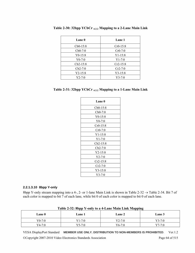
VESA DisplayPort Standard MEMBER USE ONLY. DISTRIBUTION TO NON-MEMBERS IS PROHIBITED. Ver.1.2
©Copyright 2007-2010 Video Electronics Standards Association Page 64 of 515
Table 2-30: 32bpp YCbCr 4:2:2 Mapping to a 2-Lane Main Link
Lane 0 Lane 1
Cb0-15:8 Cr0-15:8 Cb0-7:0 Cr0-7:0 Y0-15:8 Y1-15:8 Y0-7:0 Y1-7:0
Cb2-15:8 Cr2-15:8 Cb2-7:0 Cr2-7:0 Y2-15:8 Y3-15:8 Y2-7:0 Y3-7:0
Table 2-31: 32bpp YCbCr 4:2:2 Mapping to a 1-Lane Main Link
Lane 0
Cb0-15:8 Cb0-7:0 Y0-15:8 Y0-7:0
Cr0-15:8 Cr0-7:0 Y1-15:8 Y1-7:0
Cb2-15:8 Cb2-7:0 Y2-15:8 Y2-7:0
Cr2-15:8 Cr2-7:0 Y3-15:8 Y3-7:0
2.2.1.3.10 8bpp Y-only 8bpp Y-only stream mapping into a 4-, 2- or 1-lane Main Link is shown in Table 2-32 → Table 2-34. Bit 7 of each color is mapped to bit 7 of each lane, while bit 0 of each color is mapped to bit 0 of each lane.
Table 2-32: 8bpp Y-only to a 4-Lane Main Link Mapping
Lane 0 Lane 1 Lane 2 Lane 3
Y0-7:0 Y1-7:0 Y2-7:0 Y3-7:0 Y4-7:0 Y5-7:0 Y6-7:0 Y7-7:0
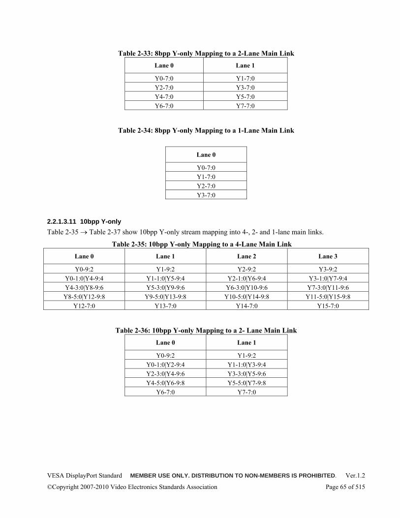
VESA DisplayPort Standard MEMBER USE ONLY. DISTRIBUTION TO NON-MEMBERS IS PROHIBITED. Ver.1.2
©Copyright 2007-2010 Video Electronics Standards Association Page 65 of 515
Table 2-33: 8bpp Y-only Mapping to a 2-Lane Main Link
Lane 0 Lane 1
Y0-7:0 Y1-7:0 Y2-7:0 Y3-7:0 Y4-7:0 Y5-7:0 Y6-7:0 Y7-7:0
Table 2-34: 8bpp Y-only Mapping to a 1-Lane Main Link
Lane 0
Y0-7:0 Y1-7:0 Y2-7:0 Y3-7:0
2.2.1.3.11 10bpp Y-only Table 2-35 → Table 2-37 show 10bpp Y-only stream mapping into 4-, 2- and 1-lane main links.
Table 2-35: 10bpp Y-only Mapping to a 4-Lane Main Link
Lane 0 Lane 1 Lane 2 Lane 3
Y0-9:2 Y1-9:2 Y2-9:2 Y3-9:2 Y0-1:0|Y4-9:4 Y1-1:0|Y5-9:4 Y2-1:0|Y6-9:4 Y3-1:0|Y7-9:4 Y4-3:0|Y8-9:6 Y5-3:0|Y9-9:6 Y6-3:0|Y10-9:6 Y7-3:0|Y11-9:6
Y8-5:0|Y12-9:8 Y9-5:0|Y13-9:8 Y10-5:0|Y14-9:8 Y11-5:0|Y15-9:8 Y12-7:0 Y13-7:0 Y14-7:0 Y15-7:0
Table 2-36: 10bpp Y-only Mapping to a 2- Lane Main Link
Lane 0 Lane 1
Y0-9:2 Y1-9:2 Y0-1:0|Y2-9:4 Y1-1:0|Y3-9:4 Y2-3:0|Y4-9:6 Y3-3:0|Y5-9:6 Y4-5:0|Y6-9:8 Y5-5:0|Y7-9:8
Y6-7:0 Y7-7:0
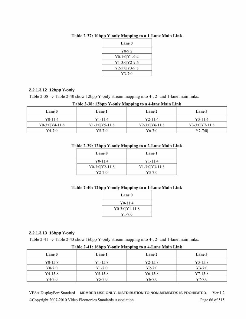
VESA DisplayPort Standard MEMBER USE ONLY. DISTRIBUTION TO NON-MEMBERS IS PROHIBITED. Ver.1.2
©Copyright 2007-2010 Video Electronics Standards Association Page 66 of 515
Table 2-37: 10bpp Y-only Mapping to a 1-Lane Main Link
Lane 0
Y0-9:2 Y0-1:0|Y1-9:4 Y1-3:0|Y2-9:6 Y2-5:0|Y3-9:8
Y3-7:0
2.2.1.3.12 12bpp Y-only Table 2-38 → Table 2-40 show 12bpp Y-only stream mapping into 4-, 2- and 1-lane main links.
Table 2-38: 12bpp Y-only Mapping to a 4-lane Main Link
Lane 0 Lane 1 Lane 2 Lane 3
Y0-11:4 Y1-11:4 Y2-11:4 Y3-11:4 Y0-3:0|Y4-11:8 Y1-3:0|Y5-11:8 Y2-3:0|Y6-11:8 Y3-3:0|Y7-11:8
Y4-7:0 Y5-7:0 Y6-7:0 Y7-7:0|
Table 2-39: 12bpp Y-only Mapping to a 2-Lane Main Link
Lane 0 Lane 1
Y0-11:4 Y1-11:4 Y0-3:0|Y2-11:8 Y1-3:0|Y3-11:8
Y2-7:0 Y3-7:0
Table 2-40: 12bpp Y-only Mapping to a 1-Lane Main Link
Lane 0
Y0-11:4 Y0-3:0|Y1-11:8
Y1-7:0
2.2.1.3.13 16bpp Y-only Table 2-41 → Table 2-43 show 16bpp Y-only stream mapping into 4-, 2- and 1-lane main links.
Table 2-41: 16bpp Y-only Mapping to a 4-Lane Main Link
Lane 0 Lane 1 Lane 2 Lane 3
Y0-15:8 Y1-15:8 Y2-15:8 Y3-15:8 Y0-7:0 Y1-7:0 Y2-7:0 Y3-7:0 Y4-15:8 Y5-15:8 Y6-15:8 Y7-15:8 Y4-7:0 Y5-7:0 Y6-7:0 Y7-7:0
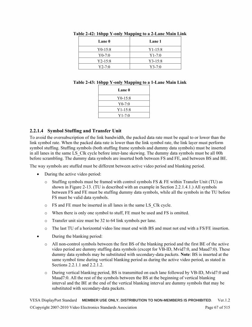
VESA DisplayPort Standard MEMBER USE ONLY. DISTRIBUTION TO NON-MEMBERS IS PROHIBITED. Ver.1.2
©Copyright 2007-2010 Video Electronics Standards Association Page 67 of 515
Table 2-42: 16bpp Y-only Mapping to a 2-Lane Main Link
Lane 0 Lane 1
Y0-15:8 Y1-15:8 Y0-7:0 Y1-7:0 Y2-15:8 Y3-15:8 Y2-7:0 Y3-7:0
Table 2-43: 16bpp Y-only Mapping to a 1-Lane Main Link
Lane 0
Y0-15:8 Y0-7:0 Y1-15:8 Y1-7:0
2.2.1.4 Symbol Stuffing and Transfer Unit To avoid the oversubscription of the link bandwidth, the packed data rate must be equal to or lower than the link symbol rate. When the packed data rate is lower than the link symbol rate, the link layer must perform symbol stuffing. Stuffing symbols (both stuffing frame symbols and dummy data symbols) must be inserted in all lanes in the same LS_Clk cycle before inter-lane skewing. The dummy data symbols must be all 00h before scrambling. The dummy data symbols are inserted both between FS and FE, and between BS and BE.
The way symbols are stuffed must be different between active video period and blanking period.
• During the active video period:
o Stuffing symbols must be framed with control symbols FS & FE within Transfer Unit (TU) as shown in Figure 2-13. (TU is described with an example in Section 2.2.1.4.1.) All symbols between FS and FE must be stuffing dummy data symbols, while all the symbols in the TU before FS must be valid data symbols.
o FS and FE must be inserted in all lanes in the same LS_Clk cycle.
o When there is only one symbol to stuff, FE must be used and FS is omitted.
o Transfer unit size must be 32 to 64 link symbols per lane.
o The last TU of a horizontal video line must end with BS and must not end with a FS/FE insertion.
• During the blanking period:
o All non-control symbols between the first BS of the blanking period and the first BE of the active video period are dummy stuffing data symbols (except for VB-ID, Mvid7:0, and Maud7:0). These dummy data symbols may be substituted with secondary-data packets. Note: BS is inserted at the same symbol time during vertical blanking period as during the active video period, as stated in Sections 2.2.1.1 and 2.2.1.2.
o During vertical blanking period, BS is transmitted on each lane followed by VB-ID, Mvid7:0 and Maud7:0. All the rest of the symbols between the BS at the beginning of vertical blanking interval and the BE at the end of the vertical blanking interval are dummy symbols that may be substituted with secondary-data packets.
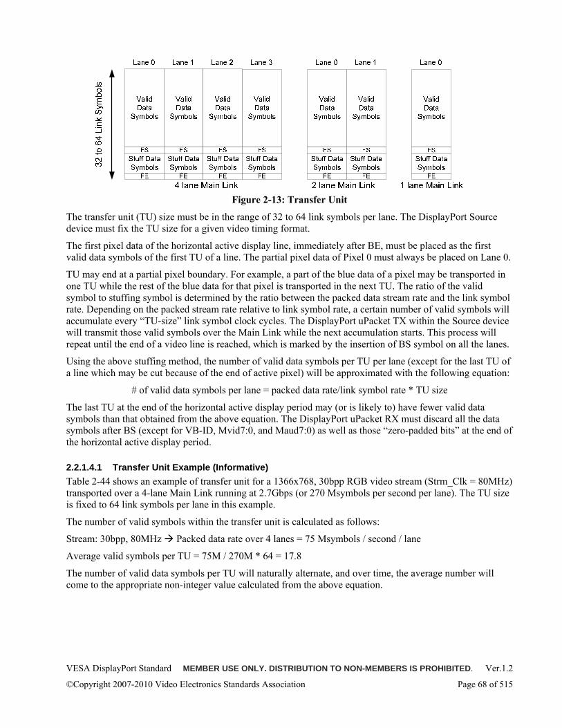
VESA DisplayPort Standard MEMBER USE ONLY. DISTRIBUTION TO NON-MEMBERS IS PROHIBITED. Ver.1.2
©Copyright 2007-2010 Video Electronics Standards Association Page 68 of 515
Figure 2-13: Transfer Unit
The transfer unit (TU) size must be in the range of 32 to 64 link symbols per lane. The DisplayPort Source device must fix the TU size for a given video timing format.
The first pixel data of the horizontal active display line, immediately after BE, must be placed as the first valid data symbols of the first TU of a line. The partial pixel data of Pixel 0 must always be placed on Lane 0.
TU may end at a partial pixel boundary. For example, a part of the blue data of a pixel may be transported in one TU while the rest of the blue data for that pixel is transported in the next TU. The ratio of the valid symbol to stuffing symbol is determined by the ratio between the packed data stream rate and the link symbol rate. Depending on the packed stream rate relative to link symbol rate, a certain number of valid symbols will accumulate every “TU-size” link symbol clock cycles. The DisplayPort uPacket TX within the Source device will transmit those valid symbols over the Main Link while the next accumulation starts. This process will repeat until the end of a video line is reached, which is marked by the insertion of BS symbol on all the lanes.
Using the above stuffing method, the number of valid data symbols per TU per lane (except for the last TU of a line which may be cut because of the end of active pixel) will be approximated with the following equation:
# of valid data symbols per lane = packed data rate/link symbol rate * TU size
The last TU at the end of the horizontal active display period may (or is likely to) have fewer valid data symbols than that obtained from the above equation. The DisplayPort uPacket RX must discard all the data symbols after BS (except for VB-ID, Mvid7:0, and Maud7:0) as well as those “zero-padded bits” at the end of the horizontal active display period.
2.2.1.4.1 Transfer Unit Example (Informative) Table 2-44 shows an example of transfer unit for a 1366x768, 30bpp RGB video stream (Strm_Clk = 80MHz) transported over a 4-lane Main Link running at 2.7Gbps (or 270 Msymbols per second per lane). The TU size is fixed to 64 link symbols per lane in this example.
The number of valid symbols within the transfer unit is calculated as follows:
Stream: 30bpp, 80MHz Packed data rate over 4 lanes = 75 Msymbols / second / lane
Average valid symbols per TU = 75M / 270M * 64 = 17.8
The number of valid data symbols per TU will naturally alternate, and over time, the average number will come to the appropriate non-integer value calculated from the above equation.
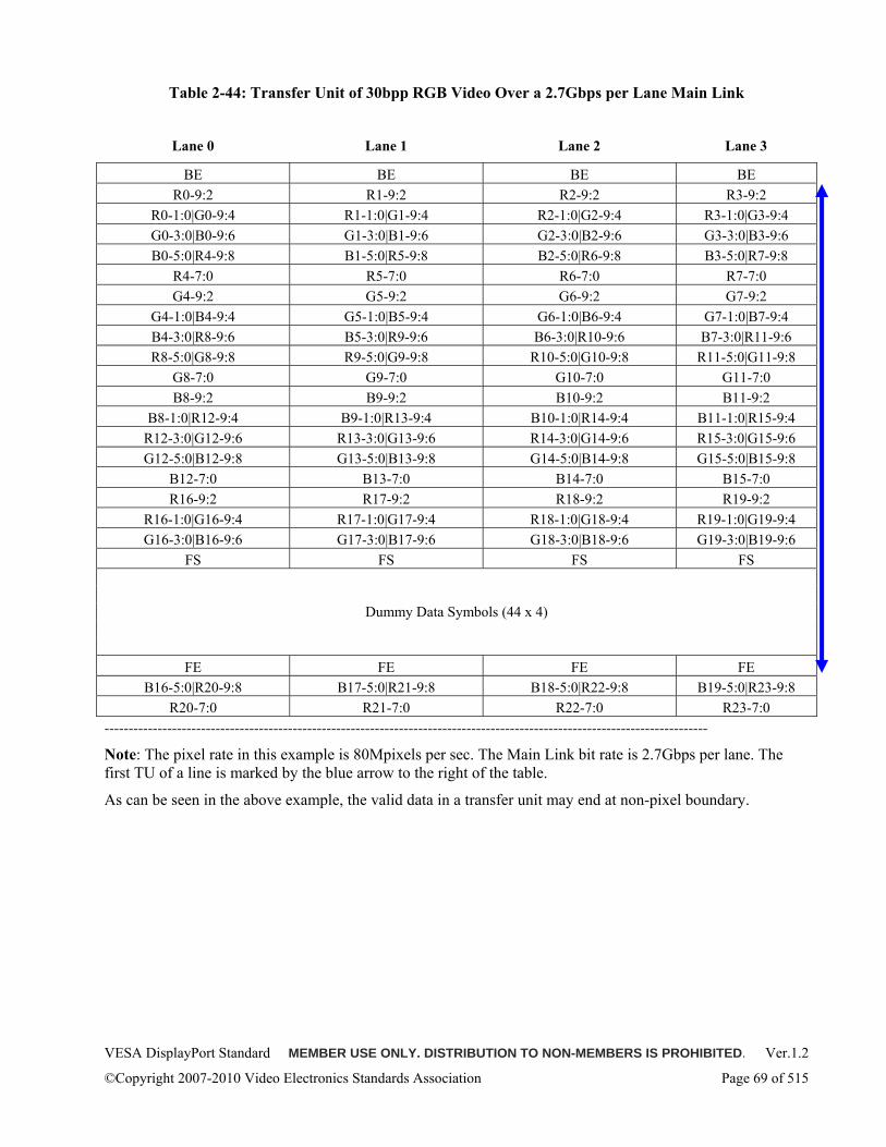
VESA DisplayPort Standard MEMBER USE ONLY. DISTRIBUTION TO NON-MEMBERS IS PROHIBITED. Ver.1.2
©Copyright 2007-2010 Video Electronics Standards Association Page 69 of 515
Table 2-44: Transfer Unit of 30bpp RGB Video Over a 2.7Gbps per Lane Main Link
Lane 0 Lane 1 Lane 2 Lane 3
BE BE BE BE R0-9:2 R1-9:2 R2-9:2 R3-9:2
R0-1:0|G0-9:4 R1-1:0|G1-9:4 R2-1:0|G2-9:4 R3-1:0|G3-9:4 G0-3:0|B0-9:6 G1-3:0|B1-9:6 G2-3:0|B2-9:6 G3-3:0|B3-9:6 B0-5:0|R4-9:8 B1-5:0|R5-9:8 B2-5:0|R6-9:8 B3-5:0|R7-9:8
R4-7:0 R5-7:0 R6-7:0 R7-7:0 G4-9:2 G5-9:2 G6-9:2 G7-9:2
G4-1:0|B4-9:4 G5-1:0|B5-9:4 G6-1:0|B6-9:4 G7-1:0|B7-9:4 B4-3:0|R8-9:6 B5-3:0|R9-9:6 B6-3:0|R10-9:6 B7-3:0|R11-9:6 R8-5:0|G8-9:8 R9-5:0|G9-9:8 R10-5:0|G10-9:8 R11-5:0|G11-9:8
G8-7:0 G9-7:0 G10-7:0 G11-7:0 B8-9:2 B9-9:2 B10-9:2 B11-9:2
B8-1:0|R12-9:4 B9-1:0|R13-9:4 B10-1:0|R14-9:4 B11-1:0|R15-9:4 R12-3:0|G12-9:6 R13-3:0|G13-9:6 R14-3:0|G14-9:6 R15-3:0|G15-9:6 G12-5:0|B12-9:8 G13-5:0|B13-9:8 G14-5:0|B14-9:8 G15-5:0|B15-9:8
B12-7:0 B13-7:0 B14-7:0 B15-7:0 R16-9:2 R17-9:2 R18-9:2 R19-9:2
R16-1:0|G16-9:4 R17-1:0|G17-9:4 R18-1:0|G18-9:4 R19-1:0|G19-9:4 G16-3:0|B16-9:6 G17-3:0|B17-9:6 G18-3:0|B18-9:6 G19-3:0|B19-9:6
FS FS FS FS
Dummy Data Symbols (44 x 4)
FE FE FE FE B16-5:0|R20-9:8 B17-5:0|R21-9:8 B18-5:0|R22-9:8 B19-5:0|R23-9:8
R20-7:0 R21-7:0 R22-7:0 R23-7:0 -----------------------------------------------------------------------------------------------------------------------------
Note: The pixel rate in this example is 80Mpixels per sec. The Main Link bit rate is 2.7Gbps per lane. The first TU of a line is marked by the blue arrow to the right of the table.
As can be seen in the above example, the valid data in a transfer unit may end at non-pixel boundary.
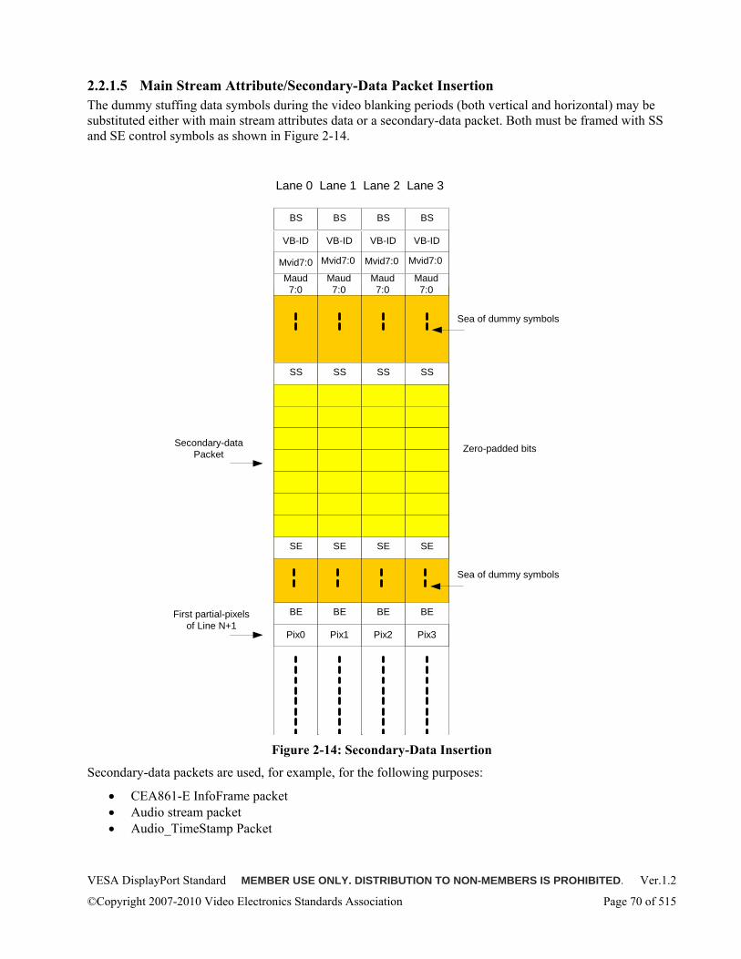
VESA DisplayPort Standard MEMBER USE ONLY. DISTRIBUTION TO NON-MEMBERS IS PROHIBITED. Ver.1.2
©Copyright 2007-2010 Video Electronics Standards Association Page 70 of 515
2.2.1.5 Main Stream Attribute/Secondary-Data Packet Insertion The dummy stuffing data symbols during the video blanking periods (both vertical and horizontal) may be substituted either with main stream attributes data or a secondary-data packet. Both must be framed with SS and SE control symbols as shown in Figure 2-14.
Secondary-dataPacket Zero-padded bits
BSPix0 Pix1 Pix2 Pix3
Sea of dummy symbols
First partial-pixelsof Line N+1
VB-IDVB-IDVB-ID VB-ID
Mvid7:0
Lane 0 Lane 1 Lane 2 Lane 3
Mvid7:0 Mvid7:0 Mvid7:0
Maud7:0
BS BS BS BS
BE BE BE BE
Maud7:0
Maud7:0
Maud7:0
BS
SS SS SS SS
BSBS
BSBS
BSBS
SE SE SE SE
Sea of dummy symbols
Figure 2-14: Secondary-Data Insertion
Secondary-data packets are used, for example, for the following purposes:
• CEA861-E InfoFrame packet • Audio stream packet • Audio_TimeStamp Packet
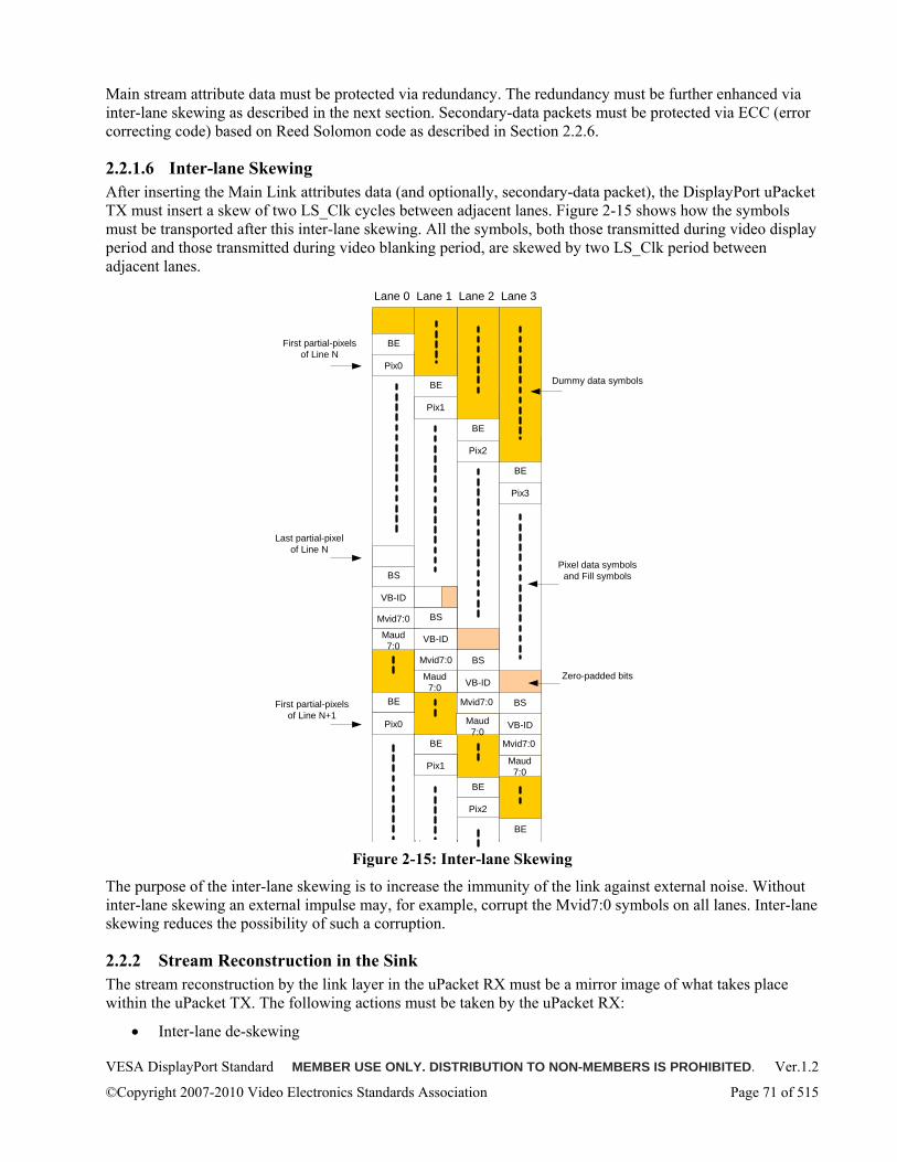
VESA DisplayPort Standard MEMBER USE ONLY. DISTRIBUTION TO NON-MEMBERS IS PROHIBITED. Ver.1.2
©Copyright 2007-2010 Video Electronics Standards Association Page 71 of 515
Main stream attribute data must be protected via redundancy. The redundancy must be further enhanced via inter-lane skewing as described in the next section. Secondary-data packets must be protected via ECC (error correcting code) based on Reed Solomon code as described in Section 2.2.6.
2.2.1.6 Inter-lane Skewing After inserting the Main Link attributes data (and optionally, secondary-data packet), the DisplayPort uPacket TX must insert a skew of two LS_Clk cycles between adjacent lanes. Figure 2-15 shows how the symbols must be transported after this inter-lane skewing. All the symbols, both those transmitted during video display period and those transmitted during video blanking period, are skewed by two LS_Clk period between adjacent lanes.
BS
First partial-pixelsof Line N
Last partial-pixelof Line N
Zero-padded bits
Pix0
Pix1
Pix2
Pix3
Pix0
Pix1
Pix2
First partial-pixelsof Line N+1
VB-ID
VB-ID
VB-ID
Mvid7:0
Lane 0 Lane 1 Lane 2 Lane 3
Mvid7:0
Mvid7:0
Mvid7:0
VB-IDMaud7:0
BS
BS
BS
BSBE
BE
BE
BE
BE
BE
BE
BE
Dummy data symbols
Pixel data symbolsand Fill symbols
Maud7:0
Maud7:0
Maud7:0
Figure 2-15: Inter-lane Skewing
The purpose of the inter-lane skewing is to increase the immunity of the link against external noise. Without inter-lane skewing an external impulse may, for example, corrupt the Mvid7:0 symbols on all lanes. Inter-lane skewing reduces the possibility of such a corruption.
2.2.2 Stream Reconstruction in the Sink The stream reconstruction by the link layer in the uPacket RX must be a mirror image of what takes place within the uPacket TX. The following actions must be taken by the uPacket RX:
• Inter-lane de-skewing
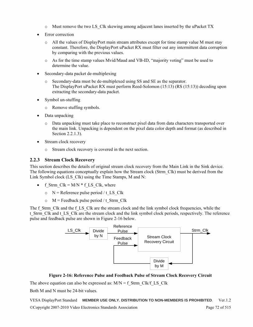
VESA DisplayPort Standard MEMBER USE ONLY. DISTRIBUTION TO NON-MEMBERS IS PROHIBITED. Ver.1.2
©Copyright 2007-2010 Video Electronics Standards Association Page 72 of 515
o Must remove the two LS_Clk skewing among adjacent lanes inserted by the uPacket TX
• Error correction
o All the values of DisplayPort main stream attributes except for time stamp value M must stay constant. Therefore, the DisplayPort uPacket RX must filter out any intermittent data corruption by comparing with the previous values.
o As for the time stamp values Mvid/Maud and VB-ID, “majority voting” must be used to determine the value.
• Secondary-data packet de-multiplexing
o Secondary-data must be de-multiplexed using SS and SE as the separator. The DisplayPort uPacket RX must perform Reed-Solomon (15:13) (RS (15:13)) decoding upon extracting the secondary-data packet.
• Symbol un-stuffing
o Remove stuffing symbols.
• Data unpacking
o Data unpacking must take place to reconstruct pixel data from data characters transported over the main link. Unpacking is dependent on the pixel data color depth and format (as described in Section 2.2.1.3).
• Stream clock recovery
o Stream clock recovery is covered in the next section.
2.2.3 Stream Clock Recovery This section describes the details of original stream clock recovery from the Main Link in the Sink device. The following equations conceptually explain how the Stream clock (Strm_Clk) must be derived from the Link Symbol clock (LS_Clk) using the Time Stamps, M and N:
• f_Strm_Clk = M/N * f_LS_Clk, where
o N = Reference pulse period / t_LS_Clk
o M = Feedback pulse period / t_Strm_Clk
The f_Strm_Clk and the f_LS_Clk are the stream clock and the link symbol clock frequencies, while the t_Strm_Clk and t_LS_Clk are the stream clock and the link symbol clock periods, respectively. The reference pulse and feedback pulse are shown in Figure 2-16 below.
Stream ClockRecovery Circuit
Divideby N
Divideby M
LS_Clk Strm_ClkReference
Pulse
FeedbackPulse
Figure 2-16: Reference Pulse and Feedback Pulse of Stream Clock Recovery Circuit
The above equation can also be expressed as: M/N = f_Strm_Clk/f_LS_Clk
Both M and N must be 24-bit values.
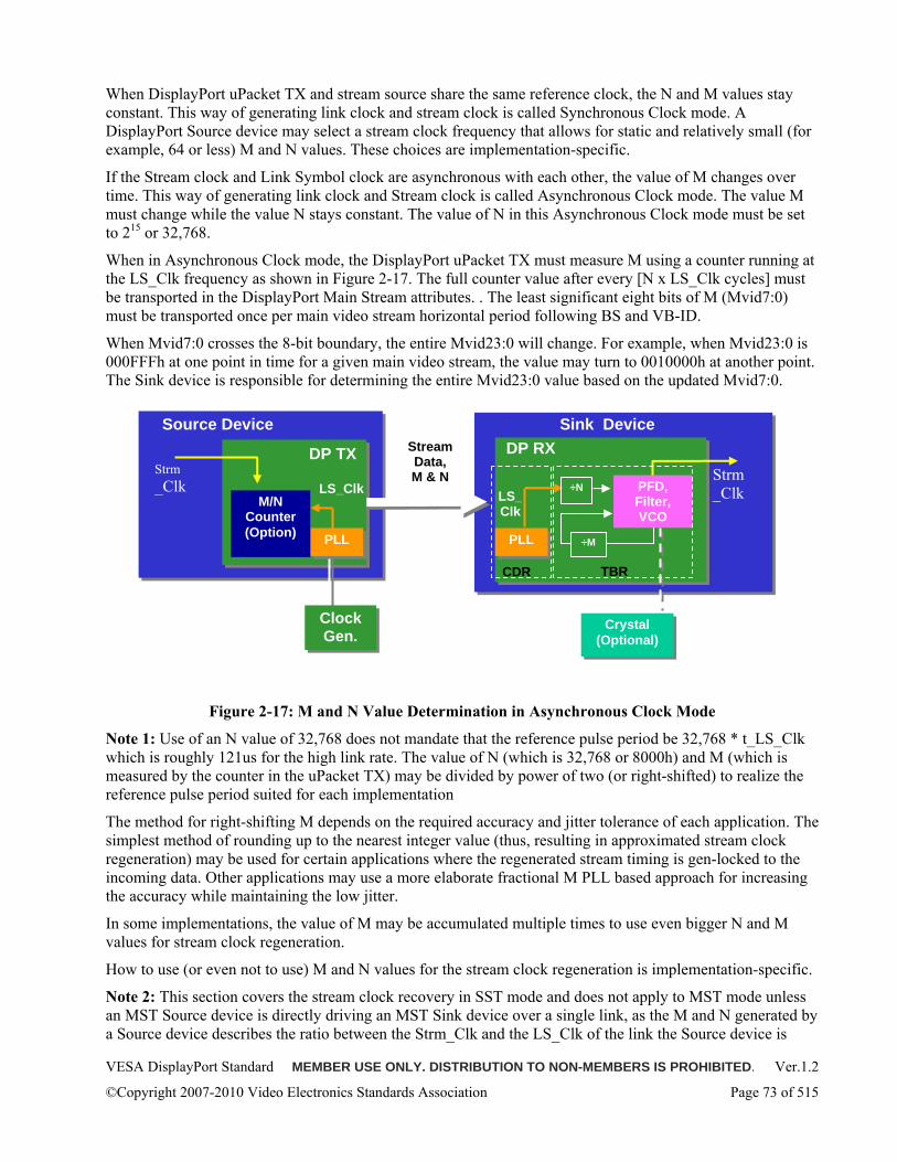
VESA DisplayPort Standard MEMBER USE ONLY. DISTRIBUTION TO NON-MEMBERS IS PROHIBITED. Ver.1.2
©Copyright 2007-2010 Video Electronics Standards Association Page 73 of 515
When DisplayPort uPacket TX and stream source share the same reference clock, the N and M values stay constant. This way of generating link clock and stream clock is called Synchronous Clock mode. A DisplayPort Source device may select a stream clock frequency that allows for static and relatively small (for example, 64 or less) M and N values. These choices are implementation-specific.
If the Stream clock and Link Symbol clock are asynchronous with each other, the value of M changes over time. This way of generating link clock and Stream clock is called Asynchronous Clock mode. The value M must change while the value N stays constant. The value of N in this Asynchronous Clock mode must be set to 215 or 32,768.
When in Asynchronous Clock mode, the DisplayPort uPacket TX must measure M using a counter running at the LS_Clk frequency as shown in Figure 2-17. The full counter value after every [N x LS_Clk cycles] must be transported in the DisplayPort Main Stream attributes. . The least significant eight bits of M (Mvid7:0) must be transported once per main video stream horizontal period following BS and VB-ID.
When Mvid7:0 crosses the 8-bit boundary, the entire Mvid23:0 will change. For example, when Mvid23:0 is 000FFFh at one point in time for a given main video stream, the value may turn to 0010000h at another point. The Sink device is responsible for determining the entire Mvid23:0 value based on the updated Mvid7:0.
Figure 2-17: M and N Value Determination in Asynchronous Clock Mode
Note 1: Use of an N value of 32,768 does not mandate that the reference pulse period be 32,768 * t_LS_Clk which is roughly 121us for the high link rate. The value of N (which is 32,768 or 8000h) and M (which is measured by the counter in the uPacket TX) may be divided by power of two (or right-shifted) to realize the reference pulse period suited for each implementation
The method for right-shifting M depends on the required accuracy and jitter tolerance of each application. The simplest method of rounding up to the nearest integer value (thus, resulting in approximated stream clock regeneration) may be used for certain applications where the regenerated stream timing is gen-locked to the incoming data. Other applications may use a more elaborate fractional M PLL based approach for increasing the accuracy while maintaining the low jitter.
In some implementations, the value of M may be accumulated multiple times to use even bigger N and M values for stream clock regeneration.
How to use (or even not to use) M and N values for the stream clock regeneration is implementation-specific.
Note 2: This section covers the stream clock recovery in SST mode and does not apply to MST mode unless an MST Source device is directly driving an MST Sink device over a single link, as the M and N generated by a Source device describes the ratio between the Strm_Clk and the LS_Clk of the link the Source device is
DP TX DP RX Source Device Sink Device
Clock Gen.
LS_Clk
PLL
÷N
÷M
LS_Clk
StreamData, M & N
PFD, Filter, VCO
CDR TBR
Strm _Clk
M/N Counter (Option)
Strm _Clk
PLL
Crystal (Optional)
VESA DisplayPort Standard MEMBER USE ONLY. DISTRIBUTION TO NON-MEMBERS IS PROHIBITED. Ver.1.2
©Copyright 2007-2010 Video Electronics Standards Association Page 74 of 515
driving. In case there are multiple links between a Source device and a Sink device, the Sink device must ignore the M and N values.
2.2.3.1 De-spreading of the Regenerated Stream Clock Support for down-spreading of the link frequency (with modulation frequencies of 30kHz ~ 33kHz) to minimize EMI is required for Sink devices compliant with the DisplayPort Standard. Support for down-spreading by uPacket TX is an implementation decision and is optional.
A DisplayPort uPacket RX must indicate whether it is capable of supporting a down-spread link frequency in the DPCD by either setting or clearing the MAX_DOWNSPREAD bit.
For a certain Sink device, such as an audio Sink device, the regenerated stream clock must not have down-spreading. Such Sink devices must perform de-spreading when regenerating the stream clock. The method of de-spreading is implementation-specific.
2.2.4 Main Stream Attribute Data Transport This section describes the Main Stream attribute data that are transported for the reproduction of the main video stream by the Sink. The attribute data is sent once per frame during the vertical blanking period of the main video stream. Those attributes must be as follows:
• M and N for main video stream clock recovery (24 bits each)
• Horizontal and vertical totals of the transmitted main video stream, in pixel and line counts, respectively (16 bits each)
• Horizontal and vertical active start from the leading edges of Hsync and Vsync in pixel and line counts, respectively (16 bits each)
• Hsync polarity/Hsync width and Vsync polarity and Vsync width in pixel and line count, respectively (1 bit for polarity and 15 bits for width)
o Hsync/Vsync polarity
0 = Active high pulse: Synchronization signal is high for the sync pulse width
1 = Active low pulse: Synchronization signal is low for the synch pulse width
• Active video width and height in pixel and line counts, respectively (16 bits each)
• Miscellaneous0 (MISC0, 8 bits)
o Synchronous Clock (bit 0)
0 = Link clock and main video stream clock asynchronous
1 = Link clock and main video stream clock synchronous When 1, the value M must be constant regardless of whether link clock down-spread enabled. This bit applies to main video stream clock, and does not apply to audio clock. (Refer to Section 2.2.5.2). Synchronousity/asynchronousity of main video stream and that of audio stream clock may be independently set.
o Colorimetry Indicator Field (bits 7:1) and bit 7 of MISC1
Refer to Section 2.2.4.3.
• Miscellaneous1 (MISC1, 8 bits)
o Interlaced vertical total even (bit 0)
0 = Number of lines per interlaced frame (consisting of two fields) is an odd number.
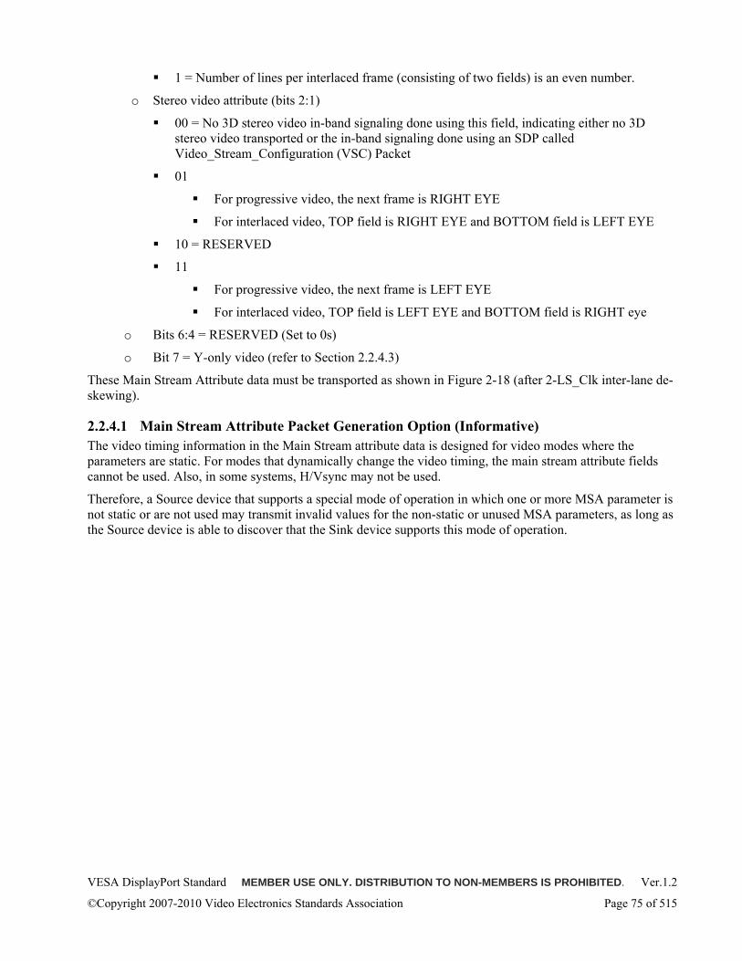
VESA DisplayPort Standard MEMBER USE ONLY. DISTRIBUTION TO NON-MEMBERS IS PROHIBITED. Ver.1.2
©Copyright 2007-2010 Video Electronics Standards Association Page 75 of 515
1 = Number of lines per interlaced frame (consisting of two fields) is an even number.
o Stereo video attribute (bits 2:1)
00 = No 3D stereo video in-band signaling done using this field, indicating either no 3D stereo video transported or the in-band signaling done using an SDP called Video_Stream_Configuration (VSC) Packet
01
For progressive video, the next frame is RIGHT EYE
For interlaced video, TOP field is RIGHT EYE and BOTTOM field is LEFT EYE
10 = RESERVED
11
For progressive video, the next frame is LEFT EYE
For interlaced video, TOP field is LEFT EYE and BOTTOM field is RIGHT eye
o Bits 6:4 = RESERVED (Set to 0s)
o Bit 7 = Y-only video (refer to Section 2.2.4.3)
These Main Stream Attribute data must be transported as shown in Figure 2-18 (after 2-LS_Clk inter-lane de-skewing).
2.2.4.1 Main Stream Attribute Packet Generation Option (Informative) The video timing information in the Main Stream attribute data is designed for video modes where the parameters are static. For modes that dynamically change the video timing, the main stream attribute fields cannot be used. Also, in some systems, H/Vsync may not be used.
Therefore, a Source device that supports a special mode of operation in which one or more MSA parameter is not static or are not used may transmit invalid values for the non-static or unused MSA parameters, as long as the Source device is able to discover that the Sink device supports this mode of operation.
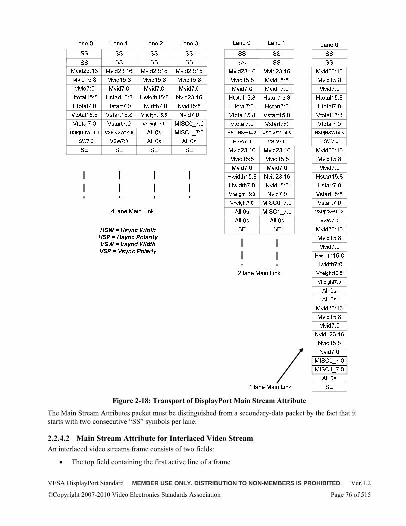
VESA DisplayPort Standard MEMBER USE ONLY. DISTRIBUTION TO NON-MEMBERS IS PROHIBITED. Ver.1.2
©Copyright 2007-2010 Video Electronics Standards Association Page 76 of 515
Figure 2-18: Transport of DisplayPort Main Stream Attribute
The Main Stream Attributes packet must be distinguished from a secondary-data packet by the fact that it starts with two consecutive “SS” symbols per lane.
2.2.4.2 Main Stream Attribute for Interlaced Video Stream An interlaced video streams frame consists of two fields:
• The top field containing the first active line of a frame
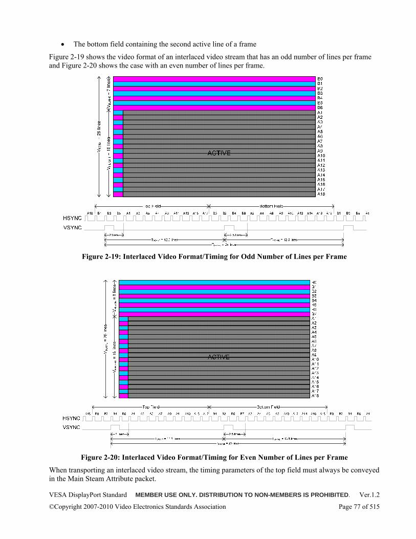
VESA DisplayPort Standard MEMBER USE ONLY. DISTRIBUTION TO NON-MEMBERS IS PROHIBITED. Ver.1.2
©Copyright 2007-2010 Video Electronics Standards Association Page 77 of 515
• The bottom field containing the second active line of a frame
Figure 2-19 shows the video format of an interlaced video stream that has an odd number of lines per frame and Figure 2-20 shows the case with an even number of lines per frame.
Figure 2-19: Interlaced Video Format/Timing for Odd Number of Lines per Frame
Figure 2-20: Interlaced Video Format/Timing for Even Number of Lines per Frame
When transporting an interlaced video stream, the timing parameters of the top field must always be conveyed in the Main Steam Attribute packet.
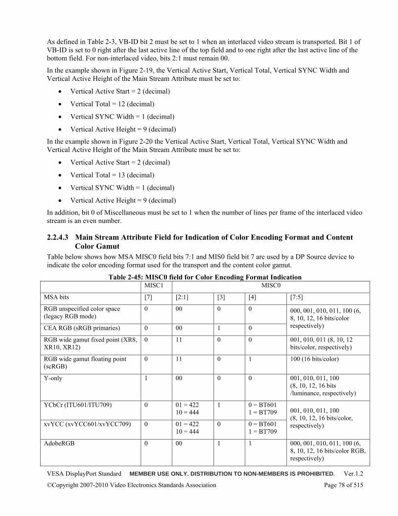
VESA DisplayPort Standard MEMBER USE ONLY. DISTRIBUTION TO NON-MEMBERS IS PROHIBITED. Ver.1.2
©Copyright 2007-2010 Video Electronics Standards Association Page 78 of 515
As defined in Table 2-3, VB-ID bit 2 must be set to 1 when an interlaced video stream is transported. Bit 1 of VB-ID is set to 0 right after the last active line of the top field and to one right after the last active line of the bottom field. For non-interlaced video, bits 2:1 must remain 00.
In the example shown in Figure 2-19, the Vertical Active Start, Vertical Total, Vertical SYNC Width and Vertical Active Height of the Main Stream Attribute must be set to:
• Vertical Active Start = 2 (decimal)
• Vertical Total = 12 (decimal)
• Vertical SYNC Width = 1 (decimal)
• Vertical Active Height = 9 (decimal)
In the example shown in Figure 2-20 the Vertical Active Start, Vertical Total, Vertical SYNC Width and Vertical Active Height of the Main Stream Attribute must be set to:
• Vertical Active Start = 2 (decimal)
• Vertical Total = 13 (decimal)
• Vertical SYNC Width = 1 (decimal)
• Vertical Active Height = 9 (decimal)
In addition, bit 0 of Miscellaneous must be set to 1 when the number of lines per frame of the interlaced video stream is an even number.
2.2.4.3 Main Stream Attribute Field for Indication of Color Encoding Format and Content Color Gamut
Table below shows how MSA MISC0 field bits 7:1 and MIS0 field bit 7 are used by a DP Source device to indicate the color encoding format used for the transport and the content color gamut.
Table 2-45: MISC0 field for Color Encoding Format Indication MISC1 MISC0
MSA bits [7] [2:1] [3] [4] [7:5]
RGB unspecified color space (legacy RGB mode)
0 00 0 0
CEA RGB (sRGB primaries) 0 00 1 0
000, 001, 010, 011, 100 (6, 8, 10, 12, 16 bits/color respectively)
RGB wide gamut fixed point (XR8, XR10, XR12)
0 11 0 0 001, 010, 011 (8, 10, 12 bits/color, respectively)
RGB wide gamut floating point (scRGB)
0 11 0 1 100 (16 bits/color)
Y-only 1 00 0 0 001, 010, 011, 100 (8, 10, 12, 16 bits /luminance, respectively)
YCbCr (ITU601/ITU709) 0 01 = 422 10 = 444
1 0 = BT601 1 = BT709
xvYCC (xvYCC601/xvYCC709) 0 01 = 422 10 = 444
0 0 = BT601 1 = BT709
001, 010, 011, 100 (8, 10, 12, 16 bits/color, respectively)
AdobeRGB 0 00 1 1 000, 001, 010, 011, 100 (6, 8, 10, 12, 16 bits/color RGB, respectively)
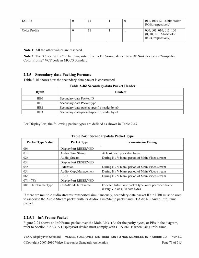
VESA DisplayPort Standard MEMBER USE ONLY. DISTRIBUTION TO NON-MEMBERS IS PROHIBITED. Ver.1.2
©Copyright 2007-2010 Video Electronics Standards Association Page 79 of 515
DCI-P3 0 11 1 0 011, 100 (12, 16 bits /color RGB, respectively)
Color Profile 0 11 1 1 000, 001, 010, 011, 100 (8, 10, 12, 16 bits/color RGB, respectively)
Note 1: All the other values are reserved.
Note 2: The “Color Profile” to be transported from a DP Source device to a DP Sink device as “Simplified Color Profile” VCP code in MCCS Standard.
2.2.5 Secondary-data Packing Formats Table 2-46 shows how the secondary-data packet is constructed.
Table 2-46: Secondary-data Packet Header
Byte# Content
HB0 Secondary-data Packet ID HB1 Secondary-data Packet type HB2 Secondary-data-packet-specific header byte0 HB3 Secondary-data-packet-specific header byte1
For DisplayPort, the following packet types are defined as shown in Table 2-47.
Table 2-47: Secondary-data Packet Type
Packet Type Value Packet Type Transmission Timing
00h DisplayPort RESERVED 01h Audio_TimeStamp At least once per video frame 02h Audio_Stream During H / V blank period of Main Video stream 03h DisplayPort RESERVED 04h Extension During H / V blank period of Main Video stream 05h Audio_CopyManagement During H / V blank period of Main Video stream 06h ISRC During H / V blank period of Main Video stream 07h - 7Fh DisplayPort RESERVED 80h + InfoFrame Type CEA-861-E InfoFrame For each InfoFrame packet type, once per video frame
during V-blank, 28 data bytes
If there are multiple audio streams transported simultaneously, secondary-data packet ID in HB0 must be used to associate the Audio Stream packet with its Audio_TimeStamp packet and CEA-861-E Audio InfoFrame packet.
2.2.5.1 InfoFrame Packet Figure 2-21 shows an InfoFrame packet over the Main Link. (As for the parity bytes, or PBs in the diagram, refer to Section 2.2.6.). A DisplayPort device must comply with CEA-861-E when using InfoFrame.
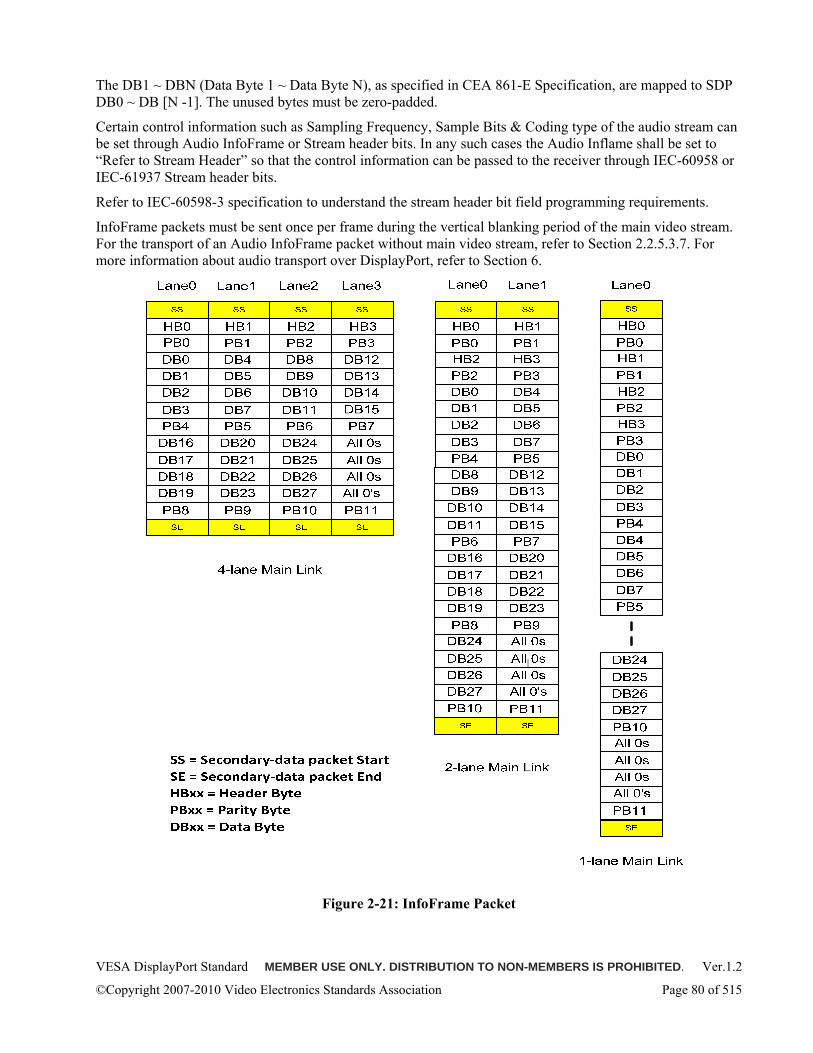
VESA DisplayPort Standard MEMBER USE ONLY. DISTRIBUTION TO NON-MEMBERS IS PROHIBITED. Ver.1.2
©Copyright 2007-2010 Video Electronics Standards Association Page 80 of 515
The DB1 ~ DBN (Data Byte 1 ~ Data Byte N), as specified in CEA 861-E Specification, are mapped to SDP DB0 ~ DB [N -1]. The unused bytes must be zero-padded.
Certain control information such as Sampling Frequency, Sample Bits & Coding type of the audio stream can be set through Audio InfoFrame or Stream header bits. In any such cases the Audio Inflame shall be set to “Refer to Stream Header” so that the control information can be passed to the receiver through IEC-60958 or IEC-61937 Stream header bits.
Refer to IEC-60598-3 specification to understand the stream header bit field programming requirements.
InfoFrame packets must be sent once per frame during the vertical blanking period of the main video stream. For the transport of an Audio InfoFrame packet without main video stream, refer to Section 2.2.5.3.7. For more information about audio transport over DisplayPort, refer to Section 6.
Figure 2-21: InfoFrame Packet
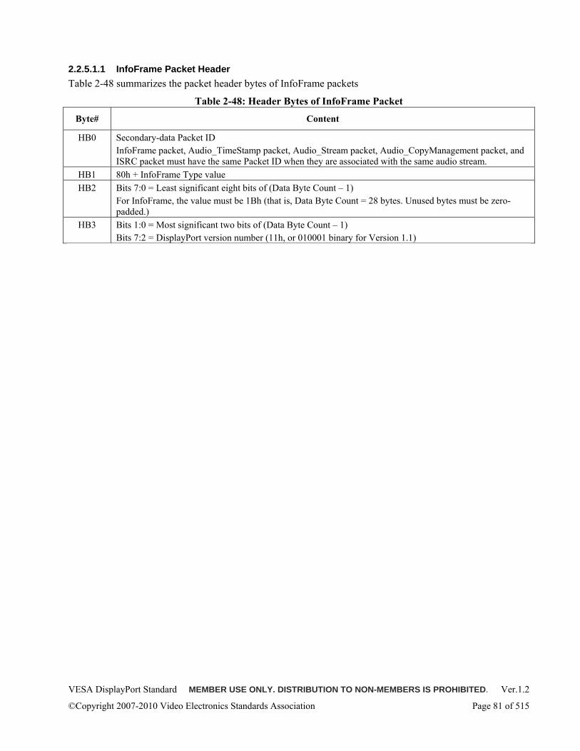
VESA DisplayPort Standard MEMBER USE ONLY. DISTRIBUTION TO NON-MEMBERS IS PROHIBITED. Ver.1.2
©Copyright 2007-2010 Video Electronics Standards Association Page 81 of 515
2.2.5.1.1 InfoFrame Packet Header Table 2-48 summarizes the packet header bytes of InfoFrame packets
Table 2-48: Header Bytes of InfoFrame Packet
Byte# Content
HB0 Secondary-data Packet ID InfoFrame packet, Audio_TimeStamp packet, Audio_Stream packet, Audio_CopyManagement packet, and ISRC packet must have the same Packet ID when they are associated with the same audio stream.
HB1 80h + InfoFrame Type value HB2 Bits 7:0 = Least significant eight bits of (Data Byte Count – 1)
For InfoFrame, the value must be 1Bh (that is, Data Byte Count = 28 bytes. Unused bytes must be zero-padded.)
HB3 Bits 1:0 = Most significant two bits of (Data Byte Count – 1) Bits 7:2 = DisplayPort version number (11h, or 010001 binary for Version 1.1)
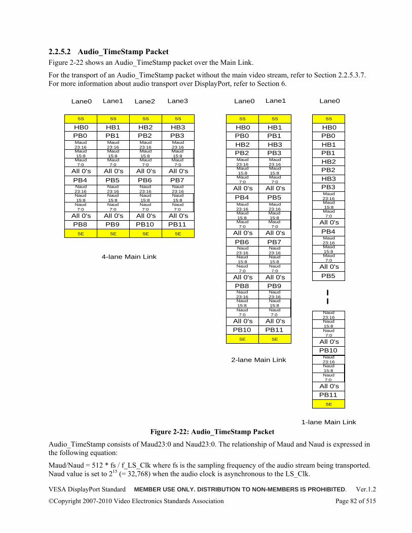
VESA DisplayPort Standard MEMBER USE ONLY. DISTRIBUTION TO NON-MEMBERS IS PROHIBITED. Ver.1.2
©Copyright 2007-2010 Video Electronics Standards Association Page 82 of 515
2.2.5.2 Audio_TimeStamp Packet Figure 2-22 shows an Audio_TimeStamp packet over the Main Link.
For the transport of an Audio_TimeStamp packet without the main video stream, refer to Section 2.2.5.3.7. For more information about audio transport over DisplayPort, refer to Section 6.
Lane3Lane2Lane1Lane0
D11
D7
D3
D10
D6
D2
D9
D5
D1
D8
D4
D0
P0
D31
D27
D23
D19
D30
D26
D22
D18
D29
D25
D21
D17
D24
D20
D16
H3
H2
H1
H0
SSSSSSSS
SESESESE
Maud23:16
M15:8M7:0All 0's
D2
D1
D0
M15:8M7:0All 0's
D2
D1
D0
M15:8M7:0All 0's D
2D
1D
0P0
M15:8M7:0All 0's
HB0 HB1 HB2 HB3
D11
D7
D3
D10
D6
D2
D9
D5
D1
D8
D4
D0
P0N23:16
N15:8N7:0
All 0's
D2
D1
D0N23:16
N15:8N7:0
All 0's
D2
D1
D0N23:16
N15:8N7:0All 0's
D2
D1
D0
P0N23:16
N15:8N7:0All 0's
D8
P0PB0 D0PB1 D0PB2 P0PB3
D8
D4
P0PB4
D0PB5
D0PB6
P0PB7
D8
D4P0PB8
D0PB9
D0PB10 P0PB11
Maud23:16
Maud23:16
Maud23:16D
8
D4P0Maud
15:8
D0
D0 P0Maud
15:8Maud15:8
Maud15:8D
8
D4P0Maud
7:0
D0
D0 P0Maud
7:0Maud7:0
Maud7:0
D10
D6
D9
D5
D1
D8
D4
D0
P0Naud
23:16
M15:8M7:0
D2
D1
D0
M15:8M7:0
D2
D1
D0
M15:8M7:0
D1
D0
P0
M15:8M7:0
Naud23:16
Naud23:16
Naud23:16
D8
D4
P0Naud
15:8
D0
D0
P0Naud
15:8Naud15:8
Naud15:8
D8
D4
P0Naud
7:0
D0
D0
P0Naud
7:0Naud7:0
Naud7:0
H1
H0
SSSS
HB0 HB1D
4
P0PB0 D0PB1
H3
H2HB2 HB3
D8
D0PB2 P0PB3
D7
D3
D6
D2
D5
D1
D4
D0
P0Maud
23:16
M15:8M7:0All 0's
D2
D1
D0
M15:8M7:0All 0's
D4
P0PB4
D0PB5
Maud23:16D
4P0Maud
15:8
D0Maud
15:8
D4P0Maud
7:0
D0Maud
7:0
D11
D10
D9
D8
D2
D1
D0
M15:8M7:0All 0's D2
D1
D0
P0
M15:8M7:0All 0's
D8
D0PB6
P0PB7
Maud23:16
Maud23:16D
8D
0 P0Maud
15:8Maud15:8D
8D
0 P0Maud
7:0Maud
7:0
D23
D19
D22
D18
D21
D17
D20
D16
D7
D3
D6
D2
D5
D1
D4
D0
P0N23:16
N15:8N7:0
All 0's
D2
D1
D0N23:16
N15:8N7:0
All 0's
D4P0PB8
D0PB9
D6
D5
D1
D4
D0
P0Naud
23:16
M15:8M7:0
D2
D1
D0
M15:8M7:0
Naud23:16
D4
P0Naud
15:8
D0Naud
15:8
D4
P0Naud
7:0
D0Naud7:0
D31
D27
D30
D26
D29
D25
D24
SESE
D11
D10
D9
D8
D2
D1
D0N23:16
N15:8N7:0All 0's
D2
D1
D0
P0N23:16
N15:8N7:0All 0's
D8
D0PB10 P0PB11
D10
D9
D8
D2
D1
D0
M15:8M7:0
D1
D0
P0
M15:8M7:0
Naud23:16
Naud23:16
D8
D0
P0Naud
15:8Naud15:8
D8
D0
P0Naud
7:0Naud7:0
H0
SS
HB0
P0PB0
H1HB1
D4
D0PB1
H2HB2
D8
D0PB2
H3HB3
P0PB3
D3
D2
D1
D0
P0Maud
23:16
M15:8M7:0All 0's
P0PB4
P0Maud
15:8
P0Maud
7:0
D7
D6
D5
D4
D2
D1
D0
M15:8M7:0All 0's
D4
D0PB5
Maud23:16D
4D
0Maud15:8
D4
D0Maud
7:0
D27
D26
D25
D24
D11
D10
D9
D8
D2
D1
D0N23:16N15:8N7:0All 0's
D8
D0PB10
D10
D9
D8
D2
D1
D0
M15:8M7:0
Naud23:16
D8
D0Naud
15:8
D8
D0Naud
7:0
D31
D30
D29
SE
D2
D1
D0
P0N23:16
N15:8N7:0All 0's
P0PB11
D1
D0
P0
M15:8M7:0
Naud23:16
P0Naud
15:8
P0Naud
7:0
Lane1Lane0 Lane0
4-lane Main Link
2-lane Main Link
1-lane Main Link Figure 2-22: Audio_TimeStamp Packet
Audio_TimeStamp consists of Maud23:0 and Naud23:0. The relationship of Maud and Naud is expressed in the following equation:
Maud/Naud = 512 * fs / f_LS_Clk where fs is the sampling frequency of the audio stream being transported. Naud value is set to 215 (= 32,768) when the audio clock is asynchronous to the LS_Clk.
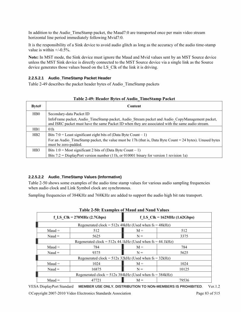
VESA DisplayPort Standard MEMBER USE ONLY. DISTRIBUTION TO NON-MEMBERS IS PROHIBITED. Ver.1.2
©Copyright 2007-2010 Video Electronics Standards Association Page 83 of 515
In addition to the Audio_TimeStamp packet, the Maud7:0 are transported once per main video stream horizontal line period immediately following Mvid7:0.
It is the responsibility of a Sink device to avoid audio glitch as long as the accuracy of the audio time-stamp value is within +/-0.5%.
Note: In MST mode, the Sink device must ignore the Maud and Mvid values sent by an MST Source device unless the MST Sink device is directly connected to the MST Source device via a single link as the Source device generates those values based on the LS_Clk of the link it is driving.
2.2.5.2.1 Audio_TimeStamp Packet Header Table 2-49 describes the packet header bytes of Audio_TimeStamp packets
Table 2-49: Header Bytes of Audio_TimeStamp Packet
Byte# Content
HB0 Secondary-data Packet ID InfoFrame packet, Audio_TimeStamp packet, Audio_Stream packet and Audio_CopyManagement packet, and ISRC packet must have the same Packet ID when they are associated with the same audio stream.
HB1 01h HB2 Bits 7:0 = Least significant eight bits of (Data Byte Count – 1)
For an Audio_TimeStamp packet, the value must be 17h (that is, Data Byte Count = 24 bytes). Unused bytes must be zero-padded.
HB3 Bits 1:0 = Most significant 2 bits of (Data Byte Count – 1) Bits 7:2 = DisplayPort version number (11h, or 010001 binary for version 1 revision 1a)
2.2.5.2.2 Audio_TimeStamp Values (Informative) Table 2-50 shows some examples of the audio time stamp values for various audio sampling frequencies when audio clock and Link Symbol clock are synchronous.
Sampling frequencies of 384KHz and 768KHz are added to support the audio high bit rate transport.
Table 2-50: Examples of Maud and Naud Values
f_LS_Clk = 270MHz (2.7Gbps) f_LS_Clk = 162MHz (1.62Gbps)
Regenerated clock = 512x 48kHz (Used when fs = 48kHz) Maud = 512 M = 512 Naud = 5625 N = 3375
Regenerated clock = 512x 44.1kHz (Used when fs = 44.1kHz) Maud = 784 M = 784 Naud = 9375 N = 5625
Regenerated clock = 512x 32kHz (Used when fs = 32kHz) Maud = 1024 M = 1024 Naud = 16875 N = 10125
Regenerated clock = 512x 384kHz (Used when fs = 384kHz) Maud = 47721 M = 79536
VESA DisplayPort Standard MEMBER USE ONLY. DISTRIBUTION TO NON-MEMBERS IS PROHIBITED. Ver.1.2
©Copyright 2007-2010 Video Electronics Standards Association Page 84 of 515
Naud = 65536 N = 65536 Regenerated clock = 512x 768kHz (Used when fs = 768kHz)
Maud = 190887 M = 318145 Naud = 131072 N = 131072
Note: No down-spreading, with synchronous clock, assumed.
2.2.5.3 Audio_Stream Packet Transport of an audio stream is optional. When an audio stream is transported, the Audio InfoFrame packet describing the attribute of the audio stream and Audio_TimeStamp packet must be also transported, each once per frame during the vertical blanking period of the main video stream.
Audio_Stream packets must be sent during both horizontal and vertical blanking periods of the main video stream. During the horizontal and vertical blanking period, DisplayPort Source device must transmit an Audio_Stream Packet whenever it has enough data to form a packet and access to the Main Link to transmit the packet(s). For more information about audio transport over DisplayPort, refer to Section 2.2.5.3 and Section 6.
When the coding type is set to “0000” it represents that encoded content equal or less than 6.144Mbps is transmitted. Coding type “0001” represents that encoded content exceeding 6.144Mbps is transmitted over the link.
IEC-61937 encoded Bit rates exceeding 6.144Mbps will be known as Audio High bit rate. DisplayPort will allow 2 different high bit rate transports such as 12.288Mbps, 24.576Mbps. These bit rates will use the following configuration to transport the data in IEC-60958 format.
• 24.576Mbps => 2 channel 16 bit and 768KHz • 12.288Mbps => 2 channel 16 bit and 384KHz
Dolby True-HD and DTS Master Audio formats require higher bit rates for transport. DisplayPort Source device shall use one of these 2 High bit rates to transmit such encoded content.
384KHz sampling rate is currently not supported in IEC-60958-3. DisplayPort will support this rate when IEC-60598-3 supports it. Until that time, it must not be used for transmitting encoded content.
There are some parameters that are available in both Audio_Stream Packet and Audio InfoFrame Packet. Parameters in Audio_Stream Packet take precedence.
2.2.5.3.1 Audio Playback Latency Requirement A DisplayPort Sink device audio recovery time from idle to playback (i.e. audio being presented to the end- user) must not exceed 50ms from the time the first Audio Sample, Audio InfoFrame or audio clock regeneration packet is received. The receiver must mute playback during recovery of local audio clock to avoid audible noise. A DisplayPort Source device may send Audio clock regeneration or InfoFrame packets prior to sending the audio stream, to ensure any recovery necessary at the DisplayPort audio receiver has completed.
2.2.5.3.2 Audio_Stream Packet Header Table 2-51 describes the packet header of an Audio_Stream packet.
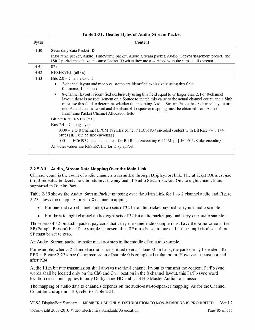
VESA DisplayPort Standard MEMBER USE ONLY. DISTRIBUTION TO NON-MEMBERS IS PROHIBITED. Ver.1.2
©Copyright 2007-2010 Video Electronics Standards Association Page 85 of 515
Table 2-51: Header Bytes of Audio_Stream Packet
Byte# Content
HB0 Secondary-data Packet ID InfoFrame packet, Audio_TimeStamp packet, Audio_Stream packet, Audio_CopyManagement packet, and ISRC packet must have the same Packet ID when they are associated with the same audio stream.
HB1 02h HB2 RESERVED (all 0s) HB3 Bits 2:0 = ChannelCount
• 2-channel layout and mono vs. stereo are identified exclusively using this field: 0 = mono, 1 = stereo
• 8-channel layout is identified exclusively using this field equal to or larger than 2. For 8-channel layout, there is no requirement on a Source to match this value to the actual channel count, and a Sink must use this field to determine whether the incoming Audio_Stream Packet has 8 channel layout or not. Actual channel count and the channel-to-speaker mapping must be obtained from Audio InfoFrame Packet Channel Allocation field.
Bit 3 = RESERVED (= 0) Bits 7:4 = Coding Type
0000 = 2 to 8 Channel LPCM 192KHz content/ IEC61937 encoded content with Bit Rate <= 6.144 Mbps [IEC 60958 like encoding] 0001 = IEC61937 encoded content for Bit Rates exceeding 6.144Mbps [IEC 60598 like encoding]
All other values are RESERVED for DisplayPort
2.2.5.3.3 Audio_Stream Data Mapping Over the Main Link Channel count is the count of audio channels transmitted through DisplayPort link. The uPacket RX must use this 3-bit value to decide how to interpret the payload of Audio Stream Packet. One to eight channels are supported in DisplayPort.
Table 2-39 shows the Audio_Stream Packet mapping over the Main Link for 1 → 2 channel audio and Figure 2-23 shows the mapping for 3 → 8 channel mapping.
• For one and two channel audio, two sets of 32-bit audio packet payload carry one audio sample
• For three to eight channel audio, eight sets of 32-bit audio packet payload carry one audio sample.
Those sets of 32-bit audio packet payloads that carry the same audio sample must have the same value in the SP (Sample Present) bit. If the sample is present then SP must be set to one and if the sample is absent then SP must be set to zero.
An Audio_Stream packet transfer must not stop in the middle of an audio sample.
For example, when a 2-channel audio is transmitted over a 1-lane Main Link, the packet may be ended after PB5 in Figure 2-23 since the transmission of sample 0 is completed at that point. However, it must not end after PB4.
Audio High bit rate transmission shall always use the 8 channel layout to transmit the content. Pa/Pb sync words shall be located only on the Ch0 and Ch1 location in the 8 channel layout, this Pa/Pb sync word location restriction applies to only Dolby True-HD and DTS HD Master Audio transmission.
The mapping of audio data to channels depends on the audio-data-to-speaker mapping. As for the Channel Count field usage in HB3, refer to Table 2-51.
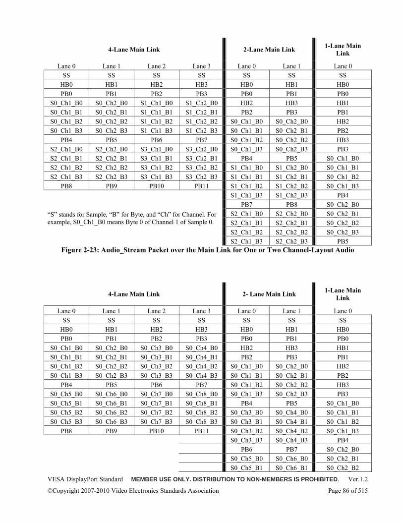
VESA DisplayPort Standard MEMBER USE ONLY. DISTRIBUTION TO NON-MEMBERS IS PROHIBITED. Ver.1.2
©Copyright 2007-2010 Video Electronics Standards Association Page 86 of 515
4-Lane Main Link 2-Lane Main Link 1-Lane Main Link
Lane 0 Lane 1 Lane 2 Lane 3 Lane 0 Lane 1 Lane 0 SS SS SS SS SS SS SS
HB0 HB1 HB2 HB3 HB0 HB1 HB0 PB0 PB1 PB2 PB3 PB0 PB1 PB0
S0_Ch1_B0 S0_Ch2_B0 S1_Ch1_B0 S1_Ch2_B0 HB2 HB3 HB1 S0_Ch1_B1 S0_Ch2_B1 S1_Ch1_B1 S1_Ch2_B1 PB2 PB3 PB1 S0_Ch1_B2 S0_Ch2_B2 S1_Ch1_B2 S1_Ch2_B2 S0_Ch1_B0 S0_Ch2_B0 HB2 S0_Ch1_B3 S0_Ch2_B3 S1_Ch1_B3 S1_Ch2_B3 S0_Ch1_B1 S0_Ch2_B1 PB2
PB4 PB5 PB6 PB7 S0_Ch1_B2 S0_Ch2_B2 HB3 S2_Ch1_B0 S2_Ch2_B0 S3_Ch1_B0 S3_Ch2_B0 S0_Ch1_B3 S0_Ch2_B3 PB3 S2_Ch1_B1 S2_Ch2_B1 S3_Ch1_B1 S3_Ch2_B1 PB4 PB5 S0_Ch1_B0 S2_Ch1_B2 S2_Ch2_B2 S3_Ch1_B2 S3_Ch2_B2 S1_Ch1_B0 S1_Ch2_B0 S0_Ch1_B1 S2_Ch1_B3 S2_Ch2_B3 S3_Ch1_B3 S3_Ch2_B3 S1_Ch1_B1 S1_Ch2_B1 S0_Ch1_B2
PB8 PB9 PB10 PB11 S1_Ch1_B2 S1_Ch2_B2 S0_Ch1_B3 S1_Ch1_B3 S1_Ch2_B3 PB4
PB7 PB8 S0_Ch2_B0 S2_Ch1_B0 S2_Ch2_B0 S0_Ch2_B1 S2_Ch1_B1 S2_Ch2_B1 S0_Ch2_B2 S2_Ch1_B2 S2_Ch2_B2 S0_Ch2_B3
“S” stands for Sample, “B” for Byte, and “Ch” for Channel. For example, S0_Ch1_B0 means Byte 0 of Channel 1 of Sample 0.
S2_Ch1_B3 S2_Ch2_B3 PB5 Figure 2-23: Audio_Stream Packet over the Main Link for One or Two Channel-Layout Audio
4-Lane Main Link 2- Lane Main Link 1-Lane Main Link
Lane 0 Lane 1 Lane 2 Lane 3 Lane 0 Lane 1 Lane 0 SS SS SS SS SS SS SS
HB0 HB1 HB2 HB3 HB0 HB1 HB0 PB0 PB1 PB2 PB3 PB0 PB1 PB0
S0_Ch1_B0 S0_Ch2_B0 S0_Ch3_B0 S0_Ch4_B0 HB2 HB3 HB1 S0_Ch1_B1 S0_Ch2_B1 S0_Ch3_B1 S0_Ch4_B1 PB2 PB3 PB1 S0_Ch1_B2 S0_Ch2_B2 S0_Ch3_B2 S0_Ch4_B2 S0_Ch1_B0 S0_Ch2_B0 HB2 S0_Ch1_B3 S0_Ch2_B3 S0_Ch3_B3 S0_Ch4_B3 S0_Ch1_B1 S0_Ch2_B1 PB2
PB4 PB5 PB6 PB7 S0_Ch1_B2 S0_Ch2_B2 HB3 S0_Ch5_B0 S0_Ch6_B0 S0_Ch7_B0 S0_Ch8_B0 S0_Ch1_B3 S0_Ch2_B3 PB3 S0_Ch5_B1 S0_Ch6_B1 S0_Ch7_B1 S0_Ch8_B1 PB4 PB5 S0_Ch1_B0 S0_Ch5_B2 S0_Ch6_B2 S0_Ch7_B2 S0_Ch8_B2 S0_Ch3_B0 S0_Ch4_B0 S0_Ch1_B1 S0_Ch5_B3 S0_Ch6_B3 S0_Ch7_B3 S0_Ch8_B3 S0_Ch3_B1 S0_Ch4_B1 S0_Ch1_B2
PB8 PB9 PB10 PB11 S0_Ch3_B2 S0_Ch4_B2 S0_Ch1_B3 S0_Ch3_B3 S0_Ch4_B3 PB4 PB6 PB7 S0_Ch2_B0 S0_Ch5_B0 S0_Ch6_B0 S0_Ch2_B1 S0_Ch5_B1 S0_Ch6_B1 S0_Ch2_B2
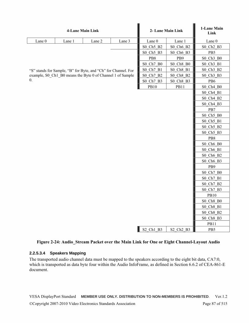
VESA DisplayPort Standard MEMBER USE ONLY. DISTRIBUTION TO NON-MEMBERS IS PROHIBITED. Ver.1.2
©Copyright 2007-2010 Video Electronics Standards Association Page 87 of 515
4-Lane Main Link 2- Lane Main Link 1-Lane Main Link
Lane 0 Lane 1 Lane 2 Lane 3 Lane 0 Lane 1 Lane 0 S0_Ch5_B2 S0_Ch6_B2 S0_Ch2_B3 S0_Ch5_B3 S0_Ch6_B3 PB5 PB8 PB9 S0_Ch3_B0
S0_Ch7_B0 S0_Ch8_B0 S0_Ch3_B1 S0_Ch7_B1 S0_Ch8_B1 S0_Ch3_B2 S0_Ch7_B2 S0_Ch8_B2 S0_Ch3_B3 S0_Ch7_B3 S0_Ch8_B3 PB6
“S” stands for Sample, “B” for Byte, and “Ch” for Channel. For example, S0_Ch1_B0 means the Byte 0 of Channel 1 of Sample 0.
PB10 PB11 S0_Ch4_B0 S0_Ch4_B1 S0_Ch4_B2 S0_Ch4_B3 PB7 S0_Ch5_B0 S0_Ch5_B1 S0_Ch5_B2 S0_Ch5_B3 PB8 S0_Ch6_B0 S0_Ch6_B1 S0_Ch6_B2 S0_Ch6_B3 PB9 S0_Ch7_B0 S0_Ch7_B1 S0_Ch7_B2 S0_Ch7_B3 PB10 S0_Ch8_B0 S0_Ch8_B1 S0_Ch8_B2 S0_Ch8_B3 PB11
S2_Ch1_B3 S2_Ch2_B3 PB5
Figure 2-24: Audio_Stream Packet over the Main Link for One or Eight Channel-Layout Audio
2.2.5.3.4 Speakers Mapping The transported audio channel data must be mapped to the speakers according to the eight bit data, CA7:0, which is transported as data byte four within the Audio InfoFrame, as defined in Section 6.6.2 of CEA-861-E document.
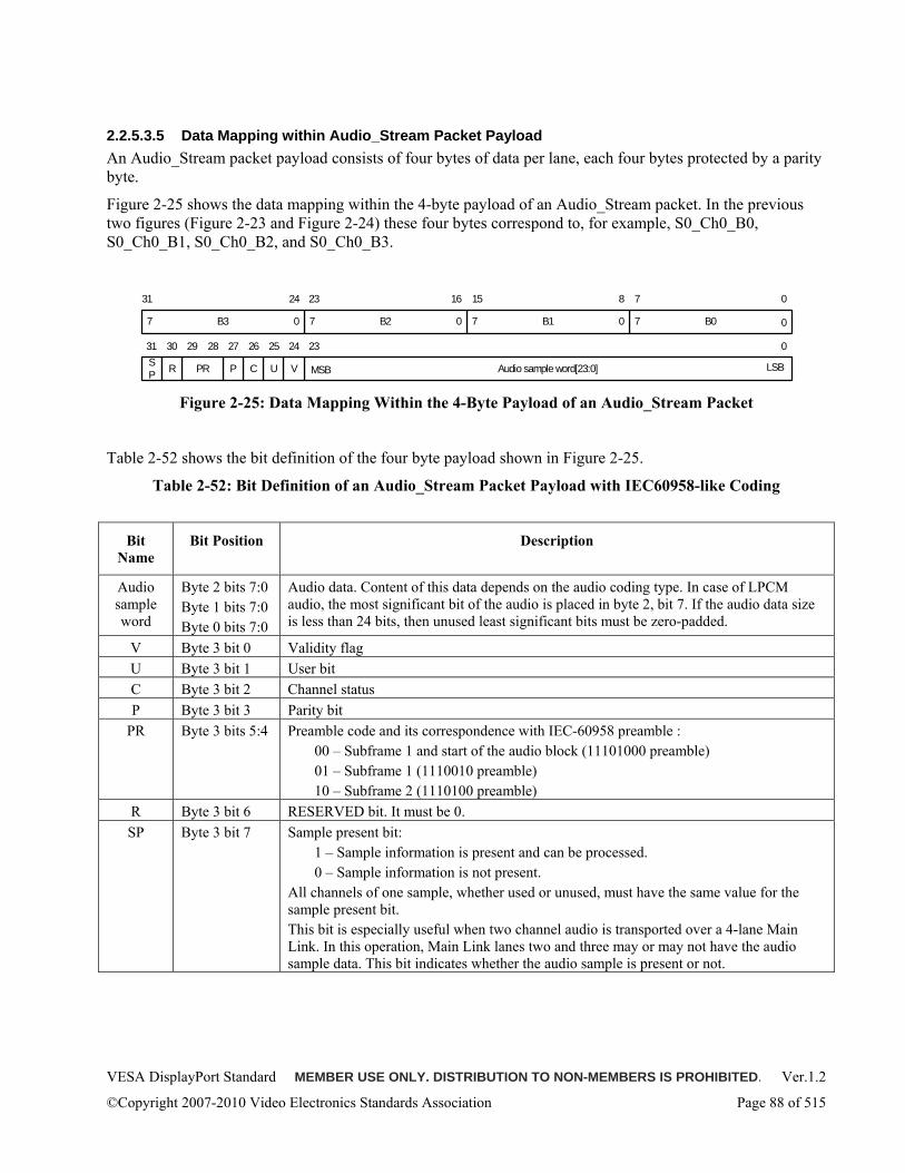
VESA DisplayPort Standard MEMBER USE ONLY. DISTRIBUTION TO NON-MEMBERS IS PROHIBITED. Ver.1.2
©Copyright 2007-2010 Video Electronics Standards Association Page 88 of 515
2.2.5.3.5 Data Mapping within Audio_Stream Packet Payload An Audio_Stream packet payload consists of four bytes of data per lane, each four bytes protected by a parity byte.
Figure 2-25 shows the data mapping within the 4-byte payload of an Audio_Stream packet. In the previous two figures (Figure 2-23 and Figure 2-24) these four bytes correspond to, for example, S0_Ch0_B0, S0_Ch0_B1, S0_Ch0_B2, and S0_Ch0_B3.
B0
Audio sample word[23:0]
0
0
MSB
781516232431
V
23
UCP
2426
LSBPRSP R
B1B2B3
252728293031
7777 0000
Figure 2-25: Data Mapping Within the 4-Byte Payload of an Audio_Stream Packet
Table 2-52 shows the bit definition of the four byte payload shown in Figure 2-25.
Table 2-52: Bit Definition of an Audio_Stream Packet Payload with IEC60958-like Coding
Bit Name
Bit Position Description
Audio sample word
Byte 2 bits 7:0 Byte 1 bits 7:0 Byte 0 bits 7:0
Audio data. Content of this data depends on the audio coding type. In case of LPCM audio, the most significant bit of the audio is placed in byte 2, bit 7. If the audio data size is less than 24 bits, then unused least significant bits must be zero-padded.
V Byte 3 bit 0 Validity flag U Byte 3 bit 1 User bit C Byte 3 bit 2 Channel status P Byte 3 bit 3 Parity bit
PR Byte 3 bits 5:4 Preamble code and its correspondence with IEC-60958 preamble : 00 – Subframe 1 and start of the audio block (11101000 preamble) 01 – Subframe 1 (1110010 preamble) 10 – Subframe 2 (1110100 preamble)
R Byte 3 bit 6 RESERVED bit. It must be 0. SP Byte 3 bit 7 Sample present bit:
1 – Sample information is present and can be processed. 0 – Sample information is not present.
All channels of one sample, whether used or unused, must have the same value for the sample present bit. This bit is especially useful when two channel audio is transported over a 4-lane Main Link. In this operation, Main Link lanes two and three may or may not have the audio sample data. This bit indicates whether the audio sample is present or not.
VESA DisplayPort Standard MEMBER USE ONLY. DISTRIBUTION TO NON-MEMBERS IS PROHIBITED. Ver.1.2
©Copyright 2007-2010 Video Electronics Standards Association Page 89 of 515
2.2.5.3.6 Other Audio Formats (Informative) DisplayPort Standard, only IEC60958-like packing format type is supported.
Using this format type and coding type of “0000”, one to eight channel LPCM, AC3, and DTS audio stream can be transported. When the coding type is “0001” Dolby True-HD and DTS Master Audio format can be transported. These encoded formats shall be transmitted by Source device only if the Sink device indicates support for receiving this encoded content. Sink device will indicate the support via short audio descriptions, (for more information refer to CEA-861 E specification). Other audio packing formats may be added in a future revision of DisplayPort Standard while maintaining the consistent secondary-data mapping specification described in this document.
Following higher bit rates will be used to transport Dolby True-HD, and DTS HD Master Audio formats.
12.288Mbps
Derived from 384KHz x 2 Channels x 16 bits
Delivered at 96KHz x 8 x 16 bits in 8 channel layout Packet Configuration
Audio time stamps shall be transmitted at Fs of 384KHz
24.576Mbps
Derived from 768KHz x 2 Channels x 16 bits
Delivered at 192KHz x 8 x 16 bits in 8 channel layout Packet Configuration
Audio time stamps shall be transmitted at Fs of 768KHz
Though the timestamps are delivered at 384 or 768KHz, the receiver may use a derivative of this timestamp to retrieve the samples.
2.2.5.3.7 Transport of Audio Packets Without Main Video Stream The DisplayPort Standard supports the transport of audio stream while no video stream is being transported over the link.
When the link is active without main video stream, a Source device must insert a BS symbol followed by VB-ID, Mvid7:0, and Maud7:0, referred to as “BS symbol set”, every 213, or 8,192 link symbols.
Both NoVideoStream_Flag and VerticalBlanking_Flag of VB-ID must be set to 1 in this condition and Mvid7:0 is set to 00h.
A Source device must transmit an Audio_Stream packet after each BS symbol set. In addition, a Source device must insert an Audio InfoFrame packet and an Audio_TimeStamp packet once after every 512th BS symbol set.
2.2.5.4 Audio_CopyManagement Packet Transport of an Audio_CopyManagement packet is an application-specific option. When an audio stream is transported and it has a specific copy management requirement from the higher level application, the Audio_CopyManagement packet describing the copy management attribute of the audio stream must be also transported. For general audio stream that has no copy management requirement, transmission of the Audio_CopyManagement packet is optional (with Copy Management Type of 00h if sent).
A DisplayPort Sink device may indicate it does not support ACM or ISRC by clearing the ACM_ISRC_sup bit in its capability declaration. In this case, DisplayPort Source device must not send any Audio_CopyManagement packet to the Sink device (on top of not sending any audio stream with copy

VESA DisplayPort Standard MEMBER USE ONLY. DISTRIBUTION TO NON-MEMBERS IS PROHIBITED. Ver.1.2
©Copyright 2007-2010 Video Electronics Standards Association Page 90 of 515
management requirement to the Sink device). If DisplayPort Sink device supports Audio_CopyManagement, and does not see the Audio_CopyManagement packet within two video frames after audio stream is transported, it shall treat the audio stream transported has no copy management requirement.
DisplayPort Source device shall support Audio_CopyManagement packet transmission if enabled by higher level application (unless Sink device does not support ACM/ISRC).
When a new audio stream with copy management requirement is transported, or if there is any change in the audio stream copy management requirements, an Audio_CopyManagement packet with up-to-date information must be transmitted within one frame of the start of transmission of the affected audio stream. The packet must continue to be sent once per frame for as long as the copy management requirement persists.
2.2.5.4.1 Audio_CopyManagement Packet Header Table 2-53 describes the packet header bytes of Audio-CopyManagement packets
Table 2-53: Header Bytes of Audio_CopyManagement Packet
Byte# Content
HB0 Secondary-data Packet ID InfoFrame packet, Audio_TimeStamp packet, Audio_Stream packet, Audio_CopyManagement packet, and ISRC packet must have the same Packet ID when they are associated with the same audio stream.
HB1 05h HB2 Bits 7:0 = Least significant eight bits of (Data Byte Count – 1)
For an Audio_CopyManagement packet, the value must be 0Fh (that is, Data Byte Count = 16 bytes. Unused bytes must be zero-padded.)
HB3 Bits 1:0 = Most significant 2 bits of (Data Byte Count – 1) Bits 7:2 = Copy Management Type
000000 = No Copy Management 000001 = IEC60958 Audio 000010 = DVD Audio 000011 – 111111 = RESERVED
Copy Management Type indicates the type of copy management associated with the audio stream.
• Value of 000000 indicates no copy management requirement is indicated by the higher level application. This is also equivalent to no transmission of Audio_CopyManagement packet.
• Value of 000001 indicates copy management is required through IEC60958 SCMS control bits, which are embedded in the audio stream channel status.
• Value of 000010 indicates DVD audio copy management is required. Please refer to DVD Specifications for Read-Only Disc, Part 4: Audio Specification, Version 1.2, for details of the copy control attributes in the data payload.
2.2.5.4.2 Audio_CopyManagement Packet Data The data payload of the Audio_CopyManagement depends on the copy management type:
• Copy management type = No Copy Management: No valid data. All 16 bytes are 0s.
• Copy management type = IEC60958 Audio: No valid data. All 16 bytes are 0s.
• Copy management type = DVD Audio: 1 byte of data content exists, with the remaining 15 bytes padded with zeros. Please refer to DVD Specifications for Read-Only Disc, Part 4: Audio Specification, Version 1.2, for details of the copy control attributes in the data content.
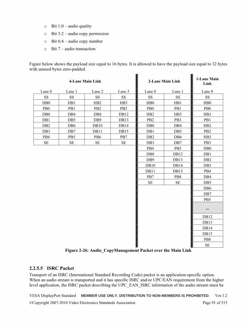
VESA DisplayPort Standard MEMBER USE ONLY. DISTRIBUTION TO NON-MEMBERS IS PROHIBITED. Ver.1.2
©Copyright 2007-2010 Video Electronics Standards Association Page 91 of 515
o Bit 1:0 – audio quality
o Bit 3:2 – audio copy permission
o Bit 6:4 – audio copy number
o Bit 7 – audio transaction
Figure below shows the payload size equal to 16 bytes. It is allowed to have the payload size equal to 32 bytes with unused bytes zero-padded.
4-Lane Main Link 2-Lane Main Link 1-Lane Main Link
Lane 0 Lane 1 Lane 2 Lane 3 Lane 0 Lane 1 Lane 0 SS SS SS SS SS SS SS
HB0 HB1 HB2 HB3 HB0 HB1 HB0 PB0 PB1 PB2 PB3 PB0 PB1 PB0 DB0 DB4 DB8 DB12 HB2 HB3 HB1 DB1 DB5 DB9 DB13 PB2 PB3 PB1 DB2 DB6 DB10 DB14 DB0 DB4 HB2 DB3 DB7 DB11 DB15 DB1 DB5 PB2 PB4 PB5 PB6 PB7 DB2 DB6 HB3 SE SE SE SE DB3 DB7 PB3
PB4 PB5 DB0 DB8 DB12 DB1 DB9 DB13 DB2 DB10 DB14 DB3 DB11 DB15 PB4 PB7 PB8 DB4 SE SE DB5
DB6 DB7 PB5
...
DB12 DB13 DB14 DB15 PB8
SE Figure 2-26: Audio_CopyManagement Packet over the Main Link
2.2.5.5 ISRC Packet Transport of an ISRC (International Standard Recording Code) packet is an application-specific option. When an audio stream is transported and it has specific ISRC and/or UPC/EAN requirement from the higher level application, the ISRC packet describing the UPC_EAN_ISRC information of the audio stream must be
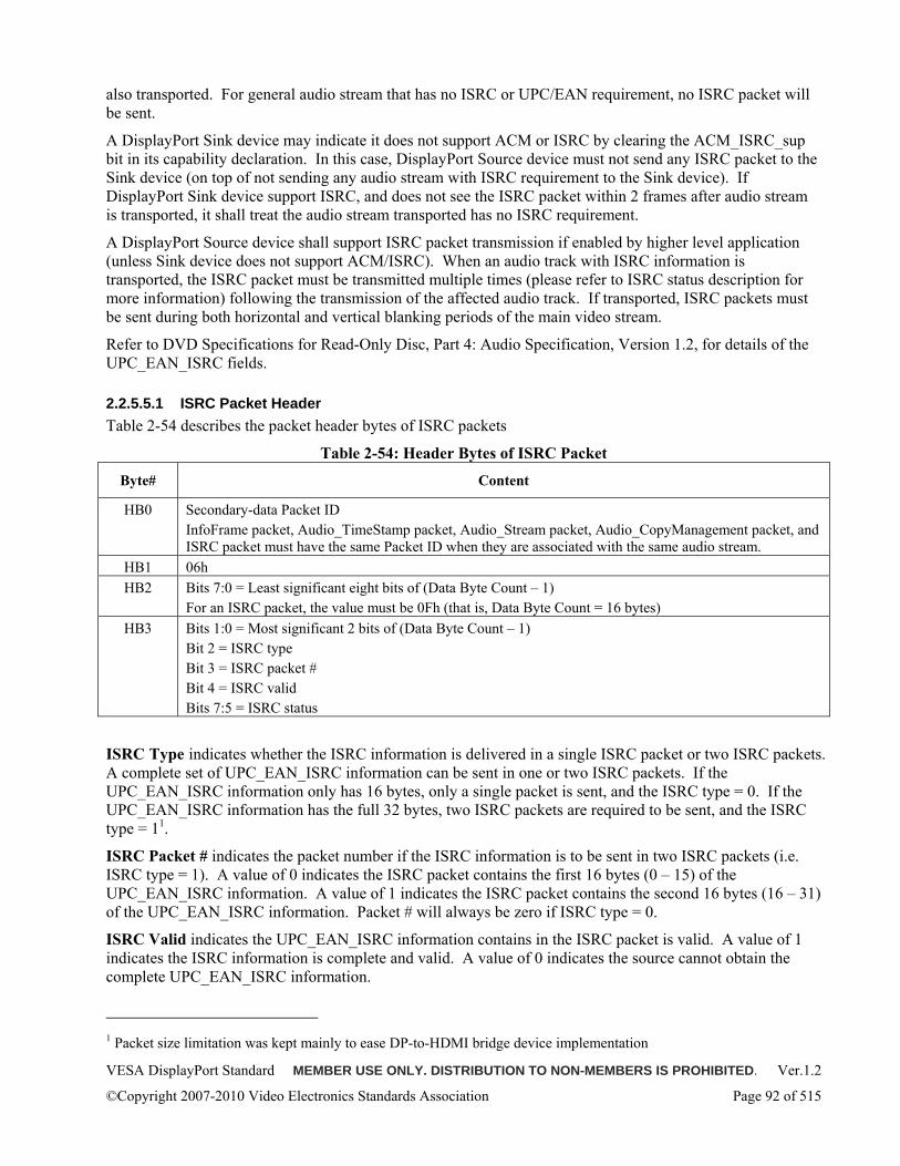
VESA DisplayPort Standard MEMBER USE ONLY. DISTRIBUTION TO NON-MEMBERS IS PROHIBITED. Ver.1.2
©Copyright 2007-2010 Video Electronics Standards Association Page 92 of 515
also transported. For general audio stream that has no ISRC or UPC/EAN requirement, no ISRC packet will be sent.
A DisplayPort Sink device may indicate it does not support ACM or ISRC by clearing the ACM_ISRC_sup bit in its capability declaration. In this case, DisplayPort Source device must not send any ISRC packet to the Sink device (on top of not sending any audio stream with ISRC requirement to the Sink device). If DisplayPort Sink device support ISRC, and does not see the ISRC packet within 2 frames after audio stream is transported, it shall treat the audio stream transported has no ISRC requirement.
A DisplayPort Source device shall support ISRC packet transmission if enabled by higher level application (unless Sink device does not support ACM/ISRC). When an audio track with ISRC information is transported, the ISRC packet must be transmitted multiple times (please refer to ISRC status description for more information) following the transmission of the affected audio track. If transported, ISRC packets must be sent during both horizontal and vertical blanking periods of the main video stream.
Refer to DVD Specifications for Read-Only Disc, Part 4: Audio Specification, Version 1.2, for details of the UPC_EAN_ISRC fields.
2.2.5.5.1 ISRC Packet Header Table 2-54 describes the packet header bytes of ISRC packets
Table 2-54: Header Bytes of ISRC Packet
Byte# Content
HB0 Secondary-data Packet ID InfoFrame packet, Audio_TimeStamp packet, Audio_Stream packet, Audio_CopyManagement packet, and ISRC packet must have the same Packet ID when they are associated with the same audio stream.
HB1 06h HB2 Bits 7:0 = Least significant eight bits of (Data Byte Count – 1)
For an ISRC packet, the value must be 0Fh (that is, Data Byte Count = 16 bytes) HB3 Bits 1:0 = Most significant 2 bits of (Data Byte Count – 1)
Bit 2 = ISRC type Bit 3 = ISRC packet # Bit 4 = ISRC valid Bits 7:5 = ISRC status
ISRC Type indicates whether the ISRC information is delivered in a single ISRC packet or two ISRC packets. A complete set of UPC_EAN_ISRC information can be sent in one or two ISRC packets. If the UPC_EAN_ISRC information only has 16 bytes, only a single packet is sent, and the ISRC type = 0. If the UPC_EAN_ISRC information has the full 32 bytes, two ISRC packets are required to be sent, and the ISRC type = 11.
ISRC Packet # indicates the packet number if the ISRC information is to be sent in two ISRC packets (i.e. ISRC type = 1). A value of 0 indicates the ISRC packet contains the first 16 bytes (0 – 15) of the UPC_EAN_ISRC information. A value of 1 indicates the ISRC packet contains the second 16 bytes (16 – 31) of the UPC_EAN_ISRC information. Packet # will always be zero if ISRC type = 0.
ISRC Valid indicates the UPC_EAN_ISRC information contains in the ISRC packet is valid. A value of 1 indicates the ISRC information is complete and valid. A value of 0 indicates the source cannot obtain the complete UPC_EAN_ISRC information.
1 Packet size limitation was kept mainly to ease DP-to-HDMI bridge device implementation
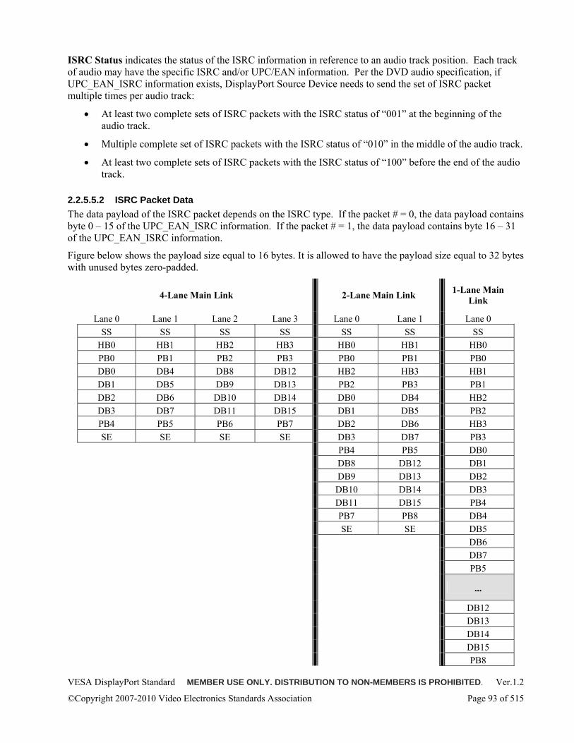
VESA DisplayPort Standard MEMBER USE ONLY. DISTRIBUTION TO NON-MEMBERS IS PROHIBITED. Ver.1.2
©Copyright 2007-2010 Video Electronics Standards Association Page 93 of 515
ISRC Status indicates the status of the ISRC information in reference to an audio track position. Each track of audio may have the specific ISRC and/or UPC/EAN information. Per the DVD audio specification, if UPC_EAN_ISRC information exists, DisplayPort Source Device needs to send the set of ISRC packet multiple times per audio track:
• At least two complete sets of ISRC packets with the ISRC status of “001” at the beginning of the audio track.
• Multiple complete set of ISRC packets with the ISRC status of “010” in the middle of the audio track.
• At least two complete sets of ISRC packets with the ISRC status of “100” before the end of the audio track.
2.2.5.5.2 ISRC Packet Data The data payload of the ISRC packet depends on the ISRC type. If the packet # = 0, the data payload contains byte 0 – 15 of the UPC_EAN_ISRC information. If the packet # = 1, the data payload contains byte 16 – 31 of the UPC_EAN_ISRC information.
Figure below shows the payload size equal to 16 bytes. It is allowed to have the payload size equal to 32 bytes with unused bytes zero-padded.
4-Lane Main Link 2-Lane Main Link 1-Lane Main Link
Lane 0 Lane 1 Lane 2 Lane 3 Lane 0 Lane 1 Lane 0 SS SS SS SS SS SS SS
HB0 HB1 HB2 HB3 HB0 HB1 HB0 PB0 PB1 PB2 PB3 PB0 PB1 PB0 DB0 DB4 DB8 DB12 HB2 HB3 HB1 DB1 DB5 DB9 DB13 PB2 PB3 PB1 DB2 DB6 DB10 DB14 DB0 DB4 HB2 DB3 DB7 DB11 DB15 DB1 DB5 PB2 PB4 PB5 PB6 PB7 DB2 DB6 HB3 SE SE SE SE DB3 DB7 PB3
PB4 PB5 DB0 DB8 DB12 DB1 DB9 DB13 DB2 DB10 DB14 DB3 DB11 DB15 PB4 PB7 PB8 DB4 SE SE DB5
DB6 DB7 PB5
...
DB12 DB13 DB14 DB15
PB8
VESA DisplayPort Standard MEMBER USE ONLY. DISTRIBUTION TO NON-MEMBERS IS PROHIBITED. Ver.1.2
©Copyright 2007-2010 Video Electronics Standards Association Page 94 of 515
SE Figure 2-27: ISRC Packet over the Main Link
2.2.5.6 Video_Stream_Configuration (VSC) Packet A DP Source device may send 3D Stereo in-band signaling using VSC Packet by setting MSA Packet MISC1 field bits 2:1 to 00.
2.2.5.6.1 VSC Packet Header Table 2-55 describes the packet header bytes of VSC Packet
Table 2-55: Header Bytes of VSC Packet
Byte# Content
HB0 Secondary-data Packet ID = 0 HB1 07h HB2 Bits 4:0 = Revision Number = 01h
Bits 7:5 = RESERVED (all 0s) HB3 Bits 4:0 = Number of valid data bytes = 01h
Bits 7:5 = RESERVED (all 0s)
2.2.5.6.2 VSC Packet Payload Table below shows the bit definitions of VSC Packet payload
Table 2-56: VSC Packet Payload DB0 bits 3:0
= Stereo Interface Method Code DB0 bits 7:4
= Stereo Interface Method-Specific Parameter 0 = Non Stereo Video Must be set to 0x0 1 = Frame/Field Sequential (Figure 6, illustrates the composited frame format as transmitted by the source)
Frame/Field Sequential Type: Value 0x0: Left & Right view indication based on the MISC1 bit 2:1 Value 0x1: Right when Stereo Signal = 1 Value 0x2: Left when Stereo Signal = 1 All other values for this field (0x3-0xF) are RESERVED for future use.
2 = Stacked Frame (Figure 7, illustrates the composited frame format as transmitted by the source)
Stacked Frame Type: Value 0x0: Left view is on top and right view on bottom All other values for this field (0x1-0xF) are RESERVED for future use.
3 = Pixel Interleaved
Interleave Pattern Type: For interleave pattern type 1 through 4, a 2x2 pattern
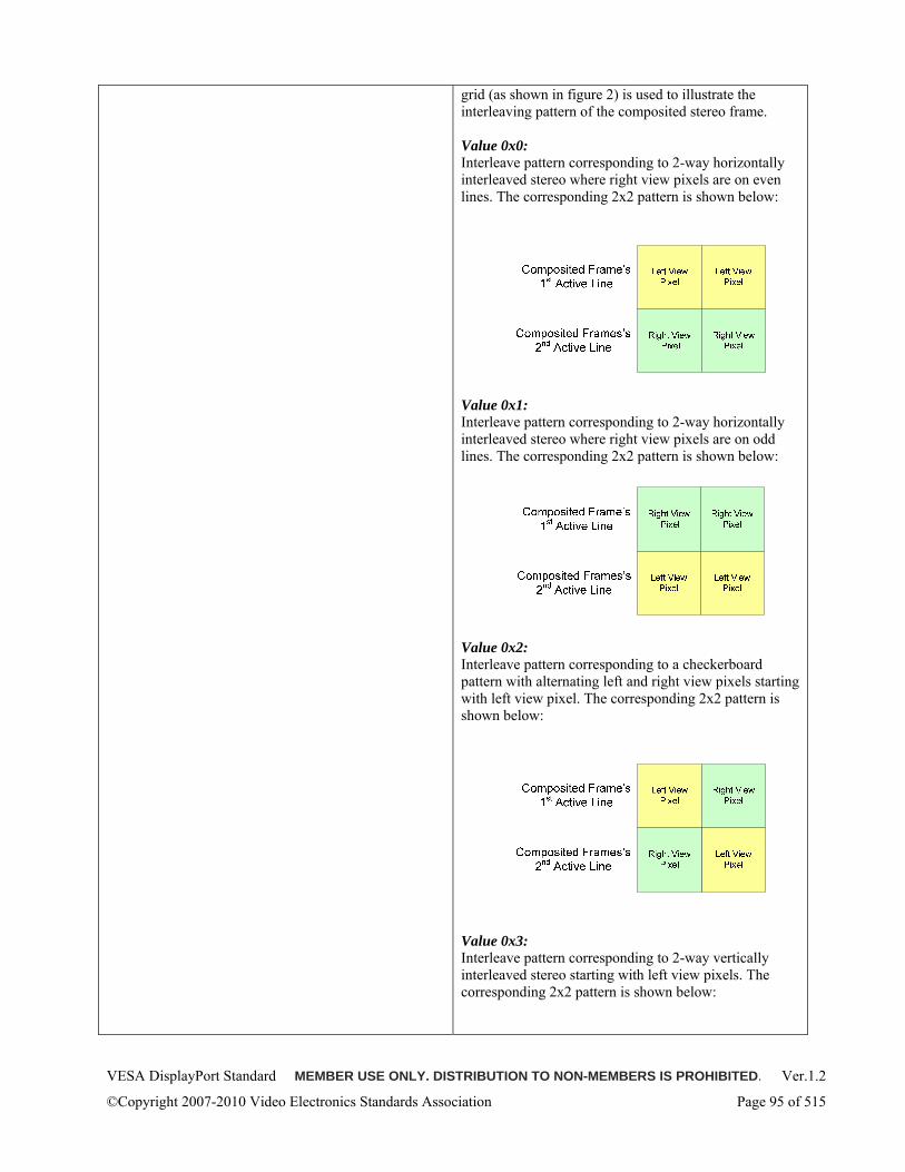
VESA DisplayPort Standard MEMBER USE ONLY. DISTRIBUTION TO NON-MEMBERS IS PROHIBITED. Ver.1.2
©Copyright 2007-2010 Video Electronics Standards Association Page 95 of 515
grid (as shown in figure 2) is used to illustrate the interleaving pattern of the composited stereo frame. Value 0x0: Interleave pattern corresponding to 2-way horizontally interleaved stereo where right view pixels are on even lines. The corresponding 2x2 pattern is shown below:
Value 0x1: Interleave pattern corresponding to 2-way horizontally interleaved stereo where right view pixels are on odd lines. The corresponding 2x2 pattern is shown below:
Value 0x2: Interleave pattern corresponding to a checkerboard pattern with alternating left and right view pixels starting with left view pixel. The corresponding 2x2 pattern is shown below:
Value 0x3: Interleave pattern corresponding to 2-way vertically interleaved stereo starting with left view pixels. The corresponding 2x2 pattern is shown below:
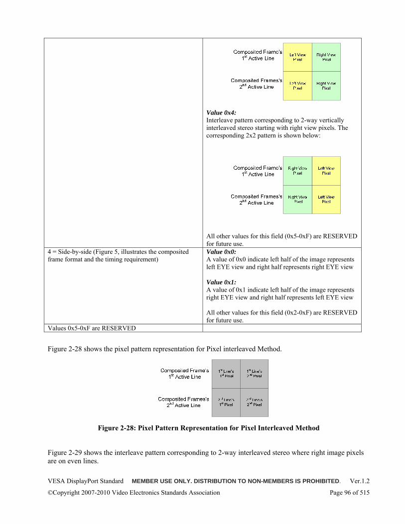
VESA DisplayPort Standard MEMBER USE ONLY. DISTRIBUTION TO NON-MEMBERS IS PROHIBITED. Ver.1.2
©Copyright 2007-2010 Video Electronics Standards Association Page 96 of 515
Value 0x4: Interleave pattern corresponding to 2-way vertically interleaved stereo starting with right view pixels. The corresponding 2x2 pattern is shown below:
All other values for this field (0x5-0xF) are RESERVED for future use.
4 = Side-by-side (Figure 5, illustrates the composited frame format and the timing requirement)
Value 0x0: A value of 0x0 indicate left half of the image represents left EYE view and right half represents right EYE view Value 0x1: A value of 0x1 indicate left half of the image represents right EYE view and right half represents left EYE view All other values for this field (0x2-0xF) are RESERVED for future use.
Values 0x5-0xF are RESERVED
Figure 2-28 shows the pixel pattern representation for Pixel interleaved Method.
Figure 2-28: Pixel Pattern Representation for Pixel Interleaved Method
Figure 2-29 shows the interleave pattern corresponding to 2-way interleaved stereo where right image pixels are on even lines.
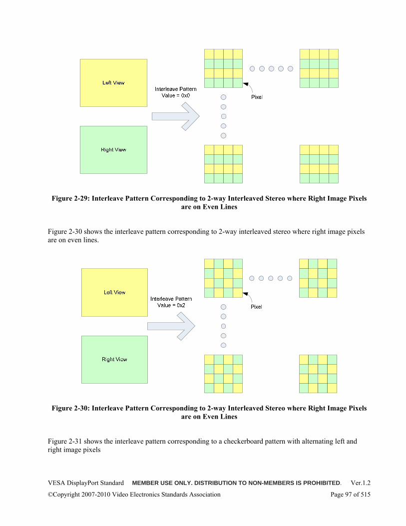
VESA DisplayPort Standard MEMBER USE ONLY. DISTRIBUTION TO NON-MEMBERS IS PROHIBITED. Ver.1.2
©Copyright 2007-2010 Video Electronics Standards Association Page 97 of 515
Figure 2-29: Interleave Pattern Corresponding to 2-way Interleaved Stereo where Right Image Pixels
are on Even Lines
Figure 2-30 shows the interleave pattern corresponding to 2-way interleaved stereo where right image pixels are on even lines.
Figure 2-30: Interleave Pattern Corresponding to 2-way Interleaved Stereo where Right Image Pixels
are on Even Lines
Figure 2-31 shows the interleave pattern corresponding to a checkerboard pattern with alternating left and right image pixels
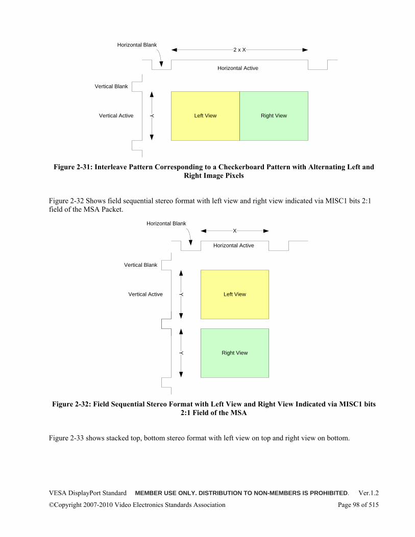
VESA DisplayPort Standard MEMBER USE ONLY. DISTRIBUTION TO NON-MEMBERS IS PROHIBITED. Ver.1.2
©Copyright 2007-2010 Video Electronics Standards Association Page 98 of 515
2 x X
Left View Right ViewY
Horizontal Active
Horizontal Blank
Vertical Blank
Vertical Active
Figure 2-31: Interleave Pattern Corresponding to a Checkerboard Pattern with Alternating Left and
Right Image Pixels
Figure 2-32 Shows field sequential stereo format with left view and right view indicated via MISC1 bits 2:1 field of the MSA Packet.
X
Left View
Right View
Y
Horizontal Active
Horizontal Blank
Vertical Blank
Vertical Active
Y
Figure 2-32: Field Sequential Stereo Format with Left View and Right View Indicated via MISC1 bits
2:1 Field of the MSA
Figure 2-33 shows stacked top, bottom stereo format with left view on top and right view on bottom.
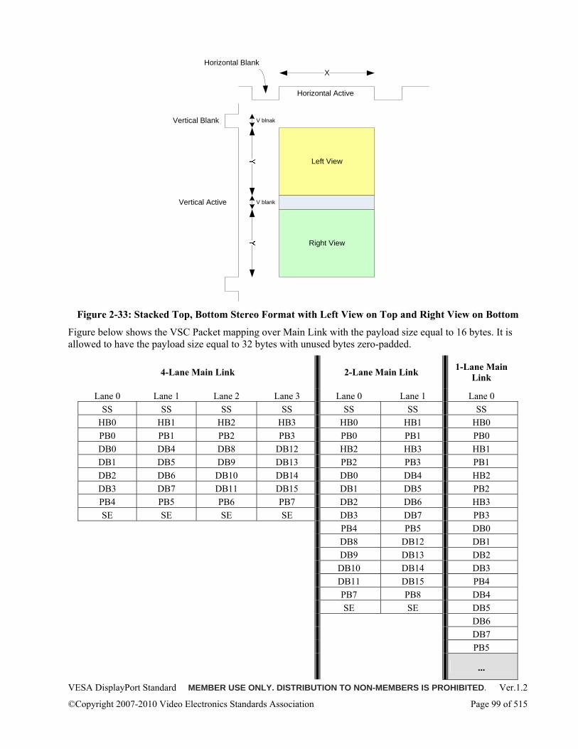
VESA DisplayPort Standard MEMBER USE ONLY. DISTRIBUTION TO NON-MEMBERS IS PROHIBITED. Ver.1.2
©Copyright 2007-2010 Video Electronics Standards Association Page 99 of 515
Left View
Right View
Vertical Blank
Vertical Active
X
Horizontal Active
Horizontal Blank
V blnak
V blank
Figure 2-33: Stacked Top, Bottom Stereo Format with Left View on Top and Right View on Bottom
Figure below shows the VSC Packet mapping over Main Link with the payload size equal to 16 bytes. It is allowed to have the payload size equal to 32 bytes with unused bytes zero-padded.
4-Lane Main Link 2-Lane Main Link 1-Lane Main Link
Lane 0 Lane 1 Lane 2 Lane 3 Lane 0 Lane 1 Lane 0 SS SS SS SS SS SS SS
HB0 HB1 HB2 HB3 HB0 HB1 HB0 PB0 PB1 PB2 PB3 PB0 PB1 PB0 DB0 DB4 DB8 DB12 HB2 HB3 HB1 DB1 DB5 DB9 DB13 PB2 PB3 PB1 DB2 DB6 DB10 DB14 DB0 DB4 HB2 DB3 DB7 DB11 DB15 DB1 DB5 PB2 PB4 PB5 PB6 PB7 DB2 DB6 HB3 SE SE SE SE DB3 DB7 PB3
PB4 PB5 DB0 DB8 DB12 DB1 DB9 DB13 DB2 DB10 DB14 DB3 DB11 DB15 PB4 PB7 PB8 DB4 SE SE DB5
DB6 DB7 PB5
...
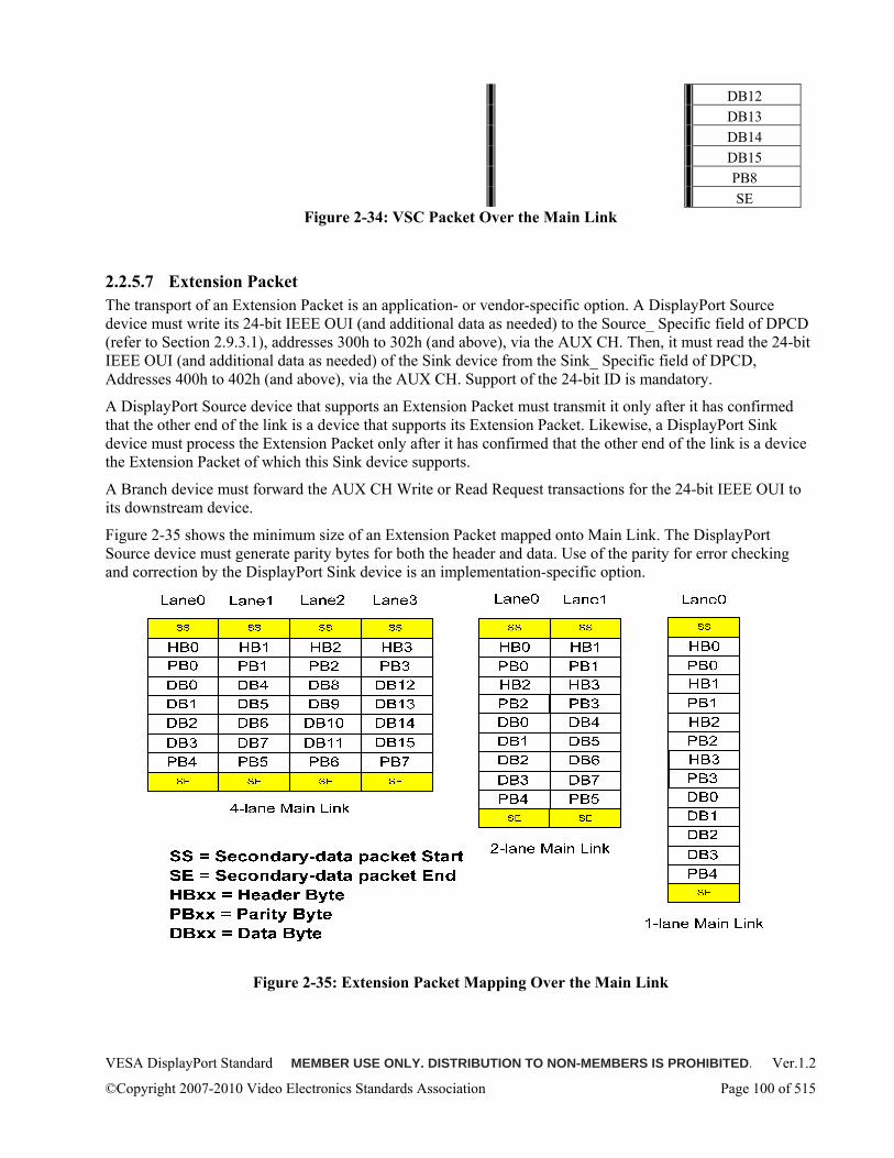
VESA DisplayPort Standard MEMBER USE ONLY. DISTRIBUTION TO NON-MEMBERS IS PROHIBITED. Ver.1.2
©Copyright 2007-2010 Video Electronics Standards Association Page 100 of 515
DB12 DB13 DB14 DB15 PB8 SE
Figure 2-34: VSC Packet Over the Main Link
2.2.5.7 Extension Packet The transport of an Extension Packet is an application- or vendor-specific option. A DisplayPort Source device must write its 24-bit IEEE OUI (and additional data as needed) to the Source_ Specific field of DPCD (refer to Section 2.9.3.1), addresses 300h to 302h (and above), via the AUX CH. Then, it must read the 24-bit IEEE OUI (and additional data as needed) of the Sink device from the Sink_ Specific field of DPCD, Addresses 400h to 402h (and above), via the AUX CH. Support of the 24-bit ID is mandatory.
A DisplayPort Source device that supports an Extension Packet must transmit it only after it has confirmed that the other end of the link is a device that supports its Extension Packet. Likewise, a DisplayPort Sink device must process the Extension Packet only after it has confirmed that the other end of the link is a device the Extension Packet of which this Sink device supports.
A Branch device must forward the AUX CH Write or Read Request transactions for the 24-bit IEEE OUI to its downstream device.
Figure 2-35 shows the minimum size of an Extension Packet mapped onto Main Link. The DisplayPort Source device must generate parity bytes for both the header and data. Use of the parity for error checking and correction by the DisplayPort Sink device is an implementation-specific option.
Figure 2-35: Extension Packet Mapping Over the Main Link
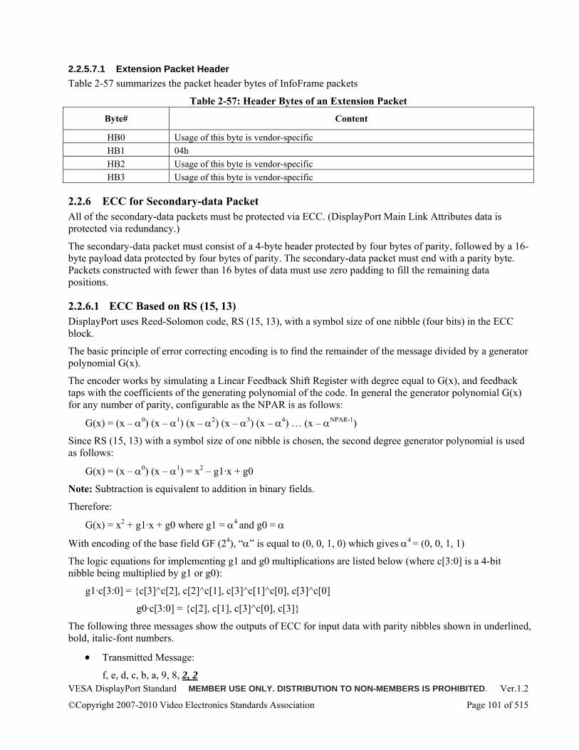
VESA DisplayPort Standard MEMBER USE ONLY. DISTRIBUTION TO NON-MEMBERS IS PROHIBITED. Ver.1.2
©Copyright 2007-2010 Video Electronics Standards Association Page 101 of 515
2.2.5.7.1 Extension Packet Header Table 2-57 summarizes the packet header bytes of InfoFrame packets
Table 2-57: Header Bytes of an Extension Packet
Byte# Content
HB0 Usage of this byte is vendor-specific HB1 04h HB2 Usage of this byte is vendor-specific HB3 Usage of this byte is vendor-specific
2.2.6 ECC for Secondary-data Packet All of the secondary-data packets must be protected via ECC. (DisplayPort Main Link Attributes data is protected via redundancy.)
The secondary-data packet must consist of a 4-byte header protected by four bytes of parity, followed by a 16- byte payload data protected by four bytes of parity. The secondary-data packet must end with a parity byte. Packets constructed with fewer than 16 bytes of data must use zero padding to fill the remaining data positions.
2.2.6.1 ECC Based on RS (15, 13) DisplayPort uses Reed-Solomon code, RS (15, 13), with a symbol size of one nibble (four bits) in the ECC block.
The basic principle of error correcting encoding is to find the remainder of the message divided by a generator polynomial G(x). The encoder works by simulating a Linear Feedback Shift Register with degree equal to G(x), and feedback taps with the coefficients of the generating polynomial of the code. In general the generator polynomial G(x) for any number of parity, configurable as the NPAR is as follows:
G(x) = (x – α0) (x – α1) (x – α2) (x – α3) (x – α4) … (x – αNPAR-1) Since RS (15, 13) with a symbol size of one nibble is chosen, the second degree generator polynomial is used as follows:
G(x) = (x – α0) (x – α1) = x2 – g1·x + g0
Note: Subtraction is equivalent to addition in binary fields. Therefore:
G(x) = x2 + g1·x + g0 where g1 = α4 and g0 = α With encoding of the base field GF (24), “α” is equal to (0, 0, 1, 0) which gives α4 = (0, 0, 1, 1) The logic equations for implementing g1 and g0 multiplications are listed below (where c[3:0] is a 4-bit nibble being multiplied by g1 or g0):
g1·c[3:0] = c[3]^c[2], c[2]^c[1], c[3]^c[1]^c[0], c[3]^c[0]
g0·c[3:0] = c[2], c[1], c[3]^c[0], c[3] The following three messages show the outputs of ECC for input data with parity nibbles shown in underlined, bold, italic-font numbers.
• Transmitted Message: f, e, d, c, b, a, 9, 8, 2, 2
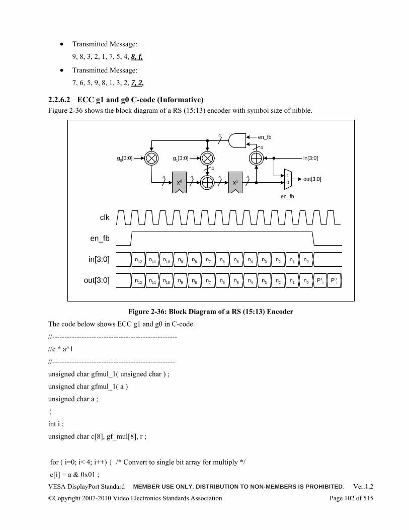
VESA DisplayPort Standard MEMBER USE ONLY. DISTRIBUTION TO NON-MEMBERS IS PROHIBITED. Ver.1.2
©Copyright 2007-2010 Video Electronics Standards Association Page 102 of 515
• Transmitted Message: 9, 8, 3, 2, 1, 7, 5, 4, 8, f,
• Transmitted Message: 7, 6, 5, 9, 8, 1, 3, 2, 7, 2,
2.2.6.2 ECC g1 and g0 C-code (Informative) Figure 2-36 shows the block diagram of a RS (15:13) encoder with symbol size of nibble.
g1[3:0]g0[3:0]
x0 x1 01
en_fb
en_fb
out[3:0]
in[3:0]
4 4 44
4
4
4
clk
en_fb
in[3:0]
out[3:0]
n10 n9 n8 n7n12 n11 n6 n5 n4 n3 n2 n1 n0
n10 n9 n8 n7n12 n11 n6 n5 n4 n3 n2 n1 n0 P1i P0
i
Figure 2-36: Block Diagram of a RS (15:13) Encoder
The code below shows ECC g1 and g0 in C-code.
//--------------------------------------------------- //c * a^1 //-------------------------------------------------- unsigned char gfmul_1( unsigned char ) ; unsigned char gfmul_1( a ) unsigned char a ; int i ; unsigned char c[8], gf_mul[8], r ; for ( i=0; i< 4; i++) /* Convert to single bit array for multiply */ c[i] = a & 0x01 ;
VESA DisplayPort Standard MEMBER USE ONLY. DISTRIBUTION TO NON-MEMBERS IS PROHIBITED. Ver.1.2
©Copyright 2007-2010 Video Electronics Standards Association Page 103 of 515
a = a >> 1 ; gf_mul[0] = c[3] ; gf_mul[1] = c[0] ^ c[3] ; gf_mul[2] = c[1] ; gf_mul[3] = c[2] ; r = 0 ; for ( i=0; i<4; i++) r = ((gf_mul[i] & 0x01) << i) | r ; return (r) ; //----------------------------------------------------- // c * a^4 //---------------------------------------------------- unsigned char gfmul_4( unsigned char ) ; unsigned char gfmul_4( a ) unsigned char a ; int i ; unsigned char c[8], gf_mul[8], r ; for ( i=0; i< 4; i++) /* Convert to single bit array for multiply */ c[i] = a & 0x01 ; a = a >> 1 ; gf_mul[0] = c[0] ^ c[3] ; gf_mul[1] = c[0] ^ c[1]^ c[3] ; gf_mul[2] = c[1] ^ c[2] ; gf_mul[3] = c[2] ^ c[3] ; r = 0 ; for ( i=0; i<4; i++) r = ((gf_mul[i] & 0x01) << i) | r ; return (r) ;
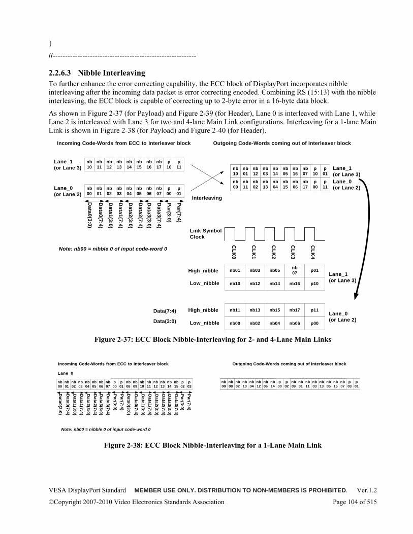
VESA DisplayPort Standard MEMBER USE ONLY. DISTRIBUTION TO NON-MEMBERS IS PROHIBITED. Ver.1.2
©Copyright 2007-2010 Video Electronics Standards Association Page 104 of 515
//----------------------------------------------------------
2.2.6.3 Nibble Interleaving To further enhance the error correcting capability, the ECC block of DisplayPort incorporates nibble interleaving after the incoming data packet is error correcting encoded. Combining RS (15:13) with the nibble interleaving, the ECC block is capable of correcting up to 2-byte error in a 16-byte data block.
As shown in Figure 2-37 (for Payload) and Figure 2-39 (for Header), Lane 0 is interleaved with Lane 1, while Lane 2 is interleaved with Lane 3 for two and 4-lane Main Link configurations. Interleaving for a 1-lane Main Link is shown in Figure 2-38 (for Payload) and Figure 2-40 (for Header).
Note: nb00 = nibble 0 of input code-word 0
Incoming Code-Words from ECC to Interleaver block Outgoing Code-Words coming out of Interleaver block
Lane_0(or Lane 2)
Lane_1(or Lane 3)
CLK
0
CLK
1
CLK
2
CLK
3
CLK
4
nb00
nb11
nb02
nb13
nb04
nb15
nb06
nb17Lane_0(or Lane 2)
Lane_0(or Lane 2)
Lane_1(or Lane 3)
nb10
nb01
nb12
nb03
nb14
nb05
nb16
nb07
p00
p11
p10
p01Lane_1(or Lane 3)
High_nibble
High_nibble
Low_nibble
Low_nibble
Link SymbolClock
Data(3:0)
Data(7:4)
Data0(3:0)
Data0(7:4)
Data1(3:0)
Data1(7:4)
Data2(3:0)
Data2(7:4)
Data3(3:0)
Data3(7:4)
Par(3:0)
Par(7:4)
nb7'
nb5'
nb3'
nb1'
nb6'
nb4'
nb2'
nb0'nb
00nb01
nb02
nb03
nb04
nb05
nb06
nb07
nb10
nb11
nb12
nb13
nb14
nb15
nb16
nb17
Interleaving
nb00
nb1
nb02
nb3
nb04
nb5
nb06
nb7
nb11
nb13
nb15
nb17
nb0
nb01
nb2
nb03
nb4
nb05
nb6
nb07
nb10
nb12
nb14
nb16
p10
p01
p00
p11
p10
p11
p00
p01
Figure 2-37: ECC Block Nibble-Interleaving for 2- and 4-Lane Main Links
Note: nb00 = nibble 0 of input code-word 0
Incoming Code-Words from ECC to Interleaver block Outgoing Code-Words coming out of Interleaver block
Lane_0
nb7'
nb5'
nb3'
nb1'
nb6'
nb4'
nb2'
nb0'nb00
nb1
nb02
nb3
nb04
nb5
nb06
nb7
nb08
nb10
nb12
nb14
nb0
nb01
nb2
nb03
nb4
nb05
nb6
nb07
nb09
nb11
nb13
nb15
p03
p01
p00
p02
nb00
nb01
nb02
nb03
nb04
nb05
nb06
nb07
Data0(3:0)
Data0(7:4)
Data1(3:0)
Data1(7:4)
Data2(3:0)
Data2(7:4)
Data3(3:0)
Data3(7:4)
Data0(3:0)
Data0(7:4)
Data1(3:0)
Data1(7:4)
Data2(3:0)
Data2(7:4)
Data3(3:0)
Data3(7:4)
Par(3:0)Par(7:4)
Par(3:0)Par(7:4)
nb08
nb09
nb10
nb11
nb12
nb13
nb14
nb15
p00
p01
p02
p03
Figure 2-38: ECC Block Nibble-Interleaving for a 1-Lane Main Link
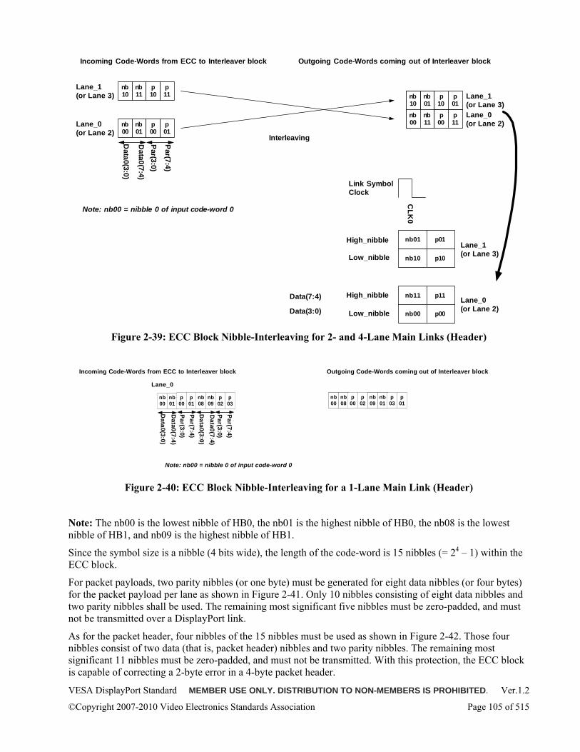
VESA DisplayPort Standard MEMBER USE ONLY. DISTRIBUTION TO NON-MEMBERS IS PROHIBITED. Ver.1.2
©Copyright 2007-2010 Video Electronics Standards Association Page 105 of 515
Note: nb00 = nibble 0 of input code-word 0
Incoming Code-Words from ECC to Interleaver block Outgoing Code-Words coming out of Interleaver block
Lane_0(or Lane 2)
Lane_1(or Lane 3)
CLK
0
nb00
nb11 Lane_0(or Lane 2)
Lane_0(or Lane 2)
Lane_1(or Lane 3)
nb10
nb01
p00
p11
p10
p01Lane_1(or Lane 3)
High_nibble
High_nibble
Low_nibble
Low_nibble
Link SymbolClock
Data(3:0)
Data(7:4)
Data0(3:0)
Data0(7:4)
Par(3:0)
Par(7:4)
nb1'
nb0'nb
00nb01
nb10
nb11
Interleaving
nb00
nb1
nb11
nb0
nb01
nb10
p10
p01
p00
p11
p10
p11
p00
p01
Figure 2-39: ECC Block Nibble-Interleaving for 2- and 4-Lane Main Links (Header)
Note: nb00 = nibble 0 of input code-word 0
Incoming Code-Words from ECC to Interleaver block Outgoing Code-Words coming out of Interleaver block
Lane_0
nb1'
nb0'nb00
nb1
nb08
nb0
nb01
nb09
p03
p01
p00
p02
nb00
nb01
Data0(3:0)
Data0(7:4)
Data0(3:0)
Data0(7:4)
Par(3:0)Par(7:4)
Par(3:0)Par(7:4)
nb08
nb09
p00
p01
p02
p03
Figure 2-40: ECC Block Nibble-Interleaving for a 1-Lane Main Link (Header)
Note: The nb00 is the lowest nibble of HB0, the nb01 is the highest nibble of HB0, the nb08 is the lowest nibble of HB1, and nb09 is the highest nibble of HB1.
Since the symbol size is a nibble (4 bits wide), the length of the code-word is 15 nibbles (= 24 – 1) within the ECC block.
For packet payloads, two parity nibbles (or one byte) must be generated for eight data nibbles (or four bytes) for the packet payload per lane as shown in Figure 2-41. Only 10 nibbles consisting of eight data nibbles and two parity nibbles shall be used. The remaining most significant five nibbles must be zero-padded, and must not be transmitted over a DisplayPort link.
As for the packet header, four nibbles of the 15 nibbles must be used as shown in Figure 2-42. Those four nibbles consist of two data (that is, packet header) nibbles and two parity nibbles. The remaining most significant 11 nibbles must be zero-padded, and must not be transmitted. With this protection, the ECC block is capable of correcting a 2-byte error in a 4-byte packet header.
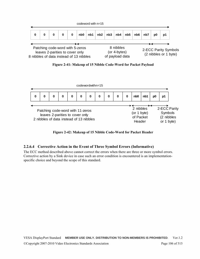
VESA DisplayPort Standard MEMBER USE ONLY. DISTRIBUTION TO NON-MEMBERS IS PROHIBITED. Ver.1.2
©Copyright 2007-2010 Video Electronics Standards Association Page 106 of 515
0 0 0 0 0 nb0 nb1 nb2 nb3 nb4 nb5 nb6 nb7 p0 p1
Patching code-word with 5-zerosleaves 2-parities to cover only
8 nibbles of data instead of 13 nibbles
8 nibbles(or 4-bytes)
of payload data
2-ECC Parity Symbols(2 nibbles or 1 byte)
codeword with n=15
Figure 2-41: Makeup of 15 Nibble Code-Word for Packet Payload
0 0 0 0 0 0 0 0 0 0 0 nb0 nb1 p0 p1
Patching code-word with 11-zerosleaves 2-parities to cover only
2 nibbles of data instead of 13 nibbles
2 nibbles(or 1 byte)of PacketHeader
2-ECC ParitySymbols(2 nibblesor 1 byte)
codeword with n=15
Figure 2-42: Makeup of 15 Nibble Code-Word for Packet Header
2.2.6.4 Corrective Action in the Event of Three Symbol Errors (Informative) The ECC method described above cannot correct the errors when there are three or more symbol errors. Corrective action by a Sink device in case such an error condition is encountered is an implementation-specific choice and beyond the scope of this standard.
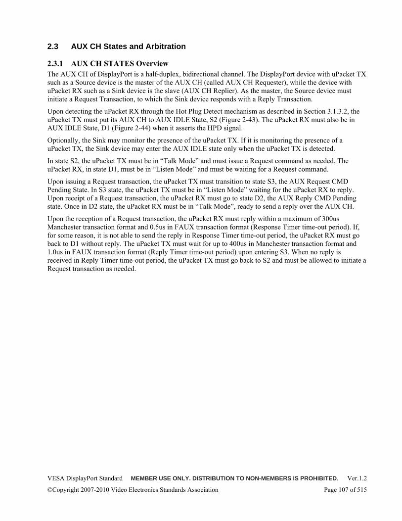
VESA DisplayPort Standard MEMBER USE ONLY. DISTRIBUTION TO NON-MEMBERS IS PROHIBITED. Ver.1.2
©Copyright 2007-2010 Video Electronics Standards Association Page 107 of 515
2.3 AUX CH States and Arbitration
2.3.1 AUX CH STATES Overview The AUX CH of DisplayPort is a half-duplex, bidirectional channel. The DisplayPort device with uPacket TX such as a Source device is the master of the AUX CH (called AUX CH Requester), while the device with uPacket RX such as a Sink device is the slave (AUX CH Replier). As the master, the Source device must initiate a Request Transaction, to which the Sink device responds with a Reply Transaction.
Upon detecting the uPacket RX through the Hot Plug Detect mechanism as described in Section 3.1.3.2, the uPacket TX must put its AUX CH to AUX IDLE State, S2 (Figure 2-43). The uPacket RX must also be in AUX IDLE State, D1 (Figure 2-44) when it asserts the HPD signal.
Optionally, the Sink may monitor the presence of the uPacket TX. If it is monitoring the presence of a uPacket TX, the Sink device may enter the AUX IDLE state only when the uPacket TX is detected.
In state S2, the uPacket TX must be in “Talk Mode” and must issue a Request command as needed. The uPacket RX, in state D1, must be in “Listen Mode” and must be waiting for a Request command.
Upon issuing a Request transaction, the uPacket TX must transition to state S3, the AUX Request CMD Pending State. In S3 state, the uPacket TX must be in “Listen Mode” waiting for the uPacket RX to reply. Upon receipt of a Request transaction, the uPacket RX must go to state D2, the AUX Reply CMD Pending state. Once in D2 state, the uPacket RX must be in “Talk Mode”, ready to send a reply over the AUX CH.
Upon the reception of a Request transaction, the uPacket RX must reply within a maximum of 300us Manchester transaction format and 0.5us in FAUX transaction format (Response Timer time-out period). If, for some reason, it is not able to send the reply in Response Timer time-out period, the uPacket RX must go back to D1 without reply. The uPacket TX must wait for up to 400us in Manchester transaction format and 1.0us in FAUX transaction format (Reply Timer time-out period) upon entering S3. When no reply is received in Reply Timer time-out period, the uPacket TX must go back to S2 and must be allowed to initiate a Request transaction as needed.
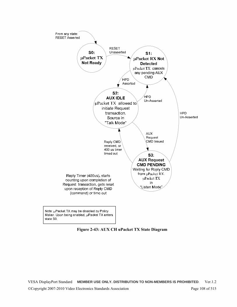
VESA DisplayPort Standard MEMBER USE ONLY. DISTRIBUTION TO NON-MEMBERS IS PROHIBITED. Ver.1.2
©Copyright 2007-2010 Video Electronics Standards Association Page 108 of 515
Figure 2-43: AUX CH uPacket TX State Diagram
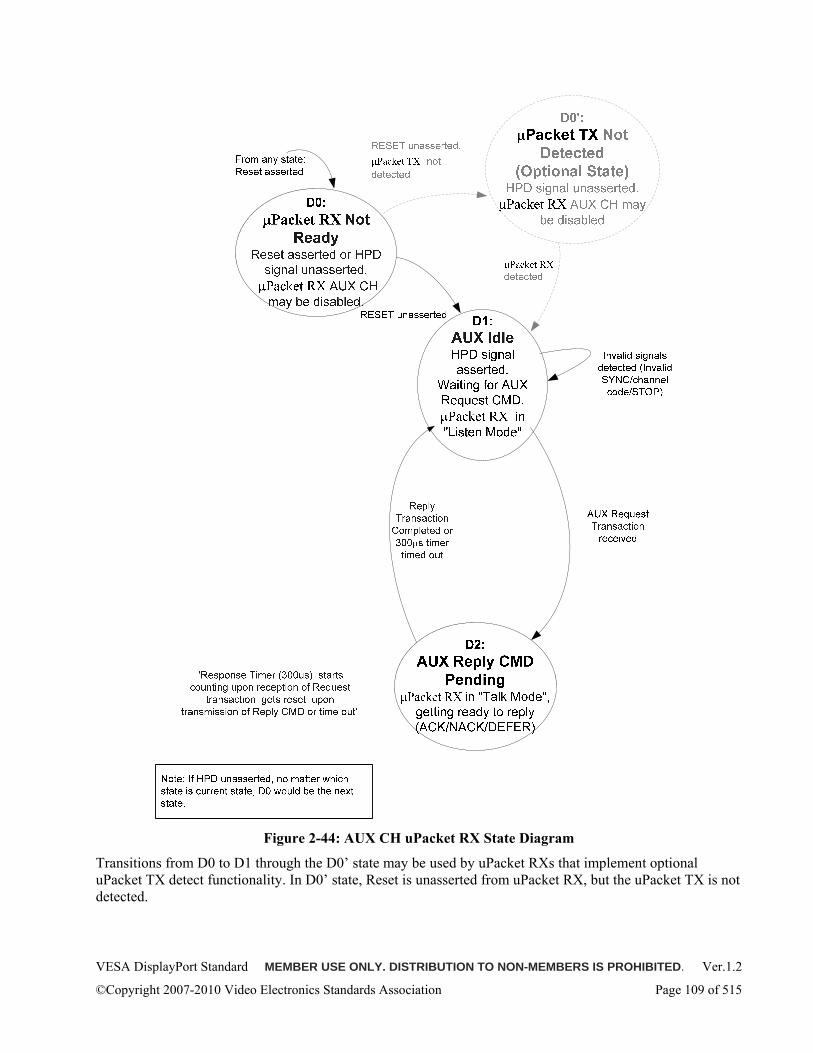
VESA DisplayPort Standard MEMBER USE ONLY. DISTRIBUTION TO NON-MEMBERS IS PROHIBITED. Ver.1.2
©Copyright 2007-2010 Video Electronics Standards Association Page 109 of 515
Figure 2-44: AUX CH uPacket RX State Diagram
Transitions from D0 to D1 through the D0’ state may be used by uPacket RXs that implement optional uPacket TX detect functionality. In D0’ state, Reset is unasserted from uPacket RX, but the uPacket TX is not detected.
VESA DisplayPort Standard MEMBER USE ONLY. DISTRIBUTION TO NON-MEMBERS IS PROHIBITED. Ver.1.2
©Copyright 2007-2010 Video Electronics Standards Association Page 110 of 515
2.3.1.1 Rules of DP_PWR State for a Source Device The rules of the DP_PWR state in conjunction with AUX CH uPacket TX State shown in Figure 2-43 for a Source device are as follows:
• In S0 state, Source device may disable DP_PWR
– Source device is either OFF (or reset) or not monitoring HPD
– Source device may go to S1 state any time
• In S1 state, Source device must enable DP_PWR
– Source device is monitoring HPD signal status
– Source device goes to S2 state when HPD signal is present
• Source device may go to S0 state any time
• In S2 and S3 states, Source device must enable DP_PWR
– Source device is either transmitting or ready to transmit (after Link Training) bits over Main Link
– Source device goes to S1 state when HPD signal is absent
• Source device may go to S0 state any time
2.3.1.2 Rules of DP_PWR State for a Sink Device The rules for the DP_PWR state in conjunction with AUX CH uPacket RX State shown in Figure 2-44 for a Sink device are as follows:
• In D0 state, a Sink device may disable DP_PWR
– Sink device is OFF (or reset) or not monitoring Source Detection signal
– Sink device de-asserts HPD signal
– Sink device may go to D1 state any time
– Sink device may go to D0’ state if it supports Source Detect feature and Source device is not detected
• In D0’ state, a Sink device must enable DP_PWR (For a tethered Sink device, upon detecting DP_PWR Consumer)
– Sink device de-asserts HPD signal, but monitors Source Detect status
– Sink device goes to D1 when Source detected
• Sink device may go to D0 state any time
• In D1 and D2 states, a Sink device must enable DP_PWR (For a tethered Sink device, upon detecting DP_PWR Consumer)
– Sink device asserts HPD signal
– Sink device is either receiving or ready to receive bits over Main Link
– Sink device goes to D0’ state when Source is absent
– Sink device stays in D1 even when Source writes 2 to Address 600h
• Sink device may go to D0 state any time
VESA DisplayPort Standard MEMBER USE ONLY. DISTRIBUTION TO NON-MEMBERS IS PROHIBITED. Ver.1.2
©Copyright 2007-2010 Video Electronics Standards Association Page 111 of 515
A Sink device may be in “Power-Save” mode even in D1 state when it is not receiving bits over Main Link. In the power save mode, the Sink device may put itself in the following condition:
• Main Link Receiver is disabled: Different signals parked at Vbias_RX
• AUX CH Receiver is monitoring differential signals: It must be ready to reply upon differential signal detection within 1ms
2.3.2 Link Layer Arbitration Control As described above, the Source and Sink devices must not to be in the Talk Mode or Listen Mode at the same time. Furthermore, the Response Timer time-out period of the Sink device must be shorter than that of Reply Timer of the Source device. In the case of a time-out, both the Source and Sink must return to the AUX IDLE state, which is Talk Mode for the Source and Listen Mode for the Sink. Therefore, contention and live lock will be avoided.
2.3.3 Policy Maker AUX CH Management There are multiple applications and services that initiate AUX transactions. Some examples are:
• AUX Link Services
o Link capability read
o Link configuration (training)
o Link status read
• AUX Device Services
o EDID read
o MCCS (Monitor Command and Control Set) control
The DisplayPort AUX CH must not support nested transactions. In other words, one transaction must be ended before another transaction can be initiated. The Policy Maker must be responsible for determining the order in which the multiple AUX Request transactions get executed per their priorities. The Link Layer shall merely initiate AUX transaction as it receives the request from the Policy Maker.
A request transaction may not end in full-completion. The Sink may reply with NACK or DEFER when not ready for full-completion. The Policy Maker must decide on the follow-up action if the Request transaction is replied with NACK or DEFER.
The amount of data transported over the AUX CH per transaction must be limited to 16 bytes or fewer (that is, the burst size must be 16 data bytes maximum) in Manchester transaction format and 64 bytes or fewer in FAUX transaction format. This limitation is set to prevent a single transaction from monopolizing the bus for an extended period of time. No transaction must occupy the AUX CH more than 500us in Manchester transaction format and 0.2us in FAUX transaction format. If a given transaction requires more than 16 bytes (in Manchester transaction format) or 64 bytes (in FAUX transaction format) of data to be transported, the Policy Maker must divide it into multiple transactions with no transaction larger than 16 or 64 bytes.
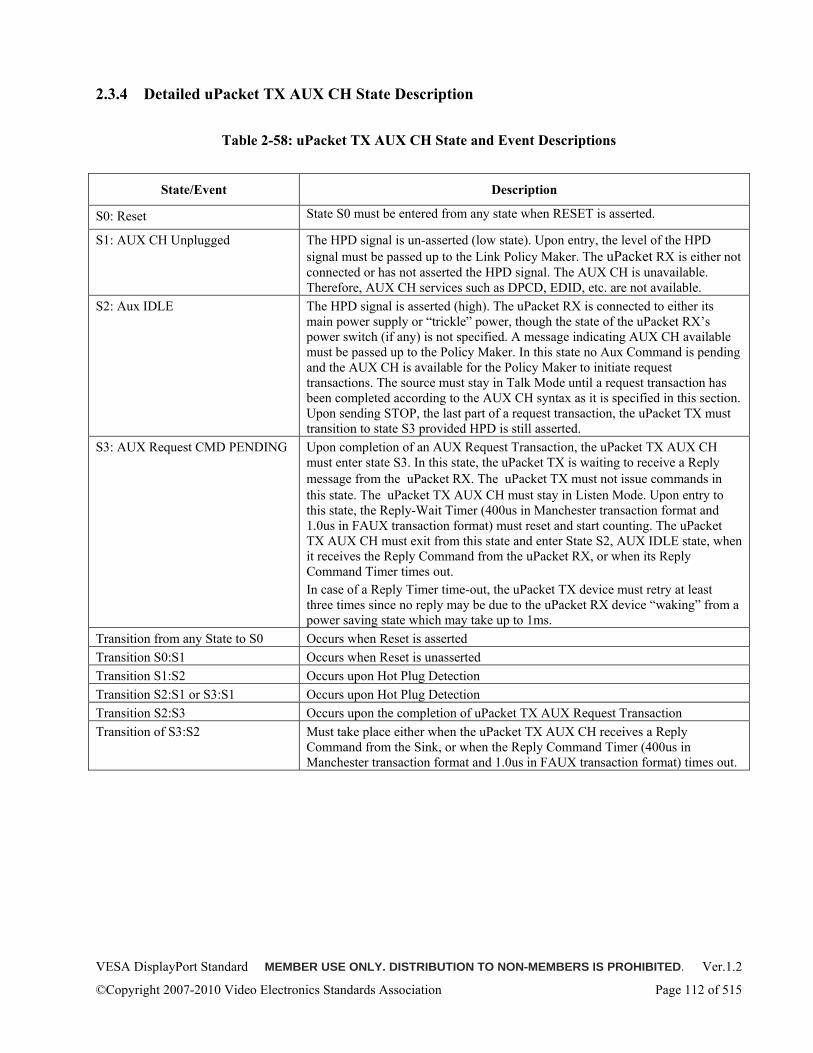
VESA DisplayPort Standard MEMBER USE ONLY. DISTRIBUTION TO NON-MEMBERS IS PROHIBITED. Ver.1.2
©Copyright 2007-2010 Video Electronics Standards Association Page 112 of 515
2.3.4 Detailed uPacket TX AUX CH State Description
Table 2-58: uPacket TX AUX CH State and Event Descriptions
State/Event Description
S0: Reset State S0 must be entered from any state when RESET is asserted.
S1: AUX CH Unplugged The HPD signal is un-asserted (low state). Upon entry, the level of the HPD signal must be passed up to the Link Policy Maker. The uPacket RX is either not connected or has not asserted the HPD signal. The AUX CH is unavailable. Therefore, AUX CH services such as DPCD, EDID, etc. are not available.
S2: Aux IDLE The HPD signal is asserted (high). The uPacket RX is connected to either its main power supply or “trickle” power, though the state of the uPacket RX’s power switch (if any) is not specified. A message indicating AUX CH available must be passed up to the Policy Maker. In this state no Aux Command is pending and the AUX CH is available for the Policy Maker to initiate request transactions. The source must stay in Talk Mode until a request transaction has been completed according to the AUX CH syntax as it is specified in this section. Upon sending STOP, the last part of a request transaction, the uPacket TX must transition to state S3 provided HPD is still asserted.
S3: AUX Request CMD PENDING Upon completion of an AUX Request Transaction, the uPacket TX AUX CH must enter state S3. In this state, the uPacket TX is waiting to receive a Reply message from the uPacket RX. The uPacket TX must not issue commands in this state. The uPacket TX AUX CH must stay in Listen Mode. Upon entry to this state, the Reply-Wait Timer (400us in Manchester transaction format and 1.0us in FAUX transaction format) must reset and start counting. The uPacket TX AUX CH must exit from this state and enter State S2, AUX IDLE state, when it receives the Reply Command from the uPacket RX, or when its Reply Command Timer times out. In case of a Reply Timer time-out, the uPacket TX device must retry at least three times since no reply may be due to the uPacket RX device “waking” from a power saving state which may take up to 1ms.
Transition from any State to S0 Occurs when Reset is asserted Transition S0:S1 Occurs when Reset is unasserted Transition S1:S2 Occurs upon Hot Plug Detection Transition S2:S1 or S3:S1 Occurs upon Hot Plug Detection Transition S2:S3 Occurs upon the completion of uPacket TX AUX Request Transaction Transition of S3:S2 Must take place either when the uPacket TX AUX CH receives a Reply
Command from the Sink, or when the Reply Command Timer (400us in Manchester transaction format and 1.0us in FAUX transaction format) times out.
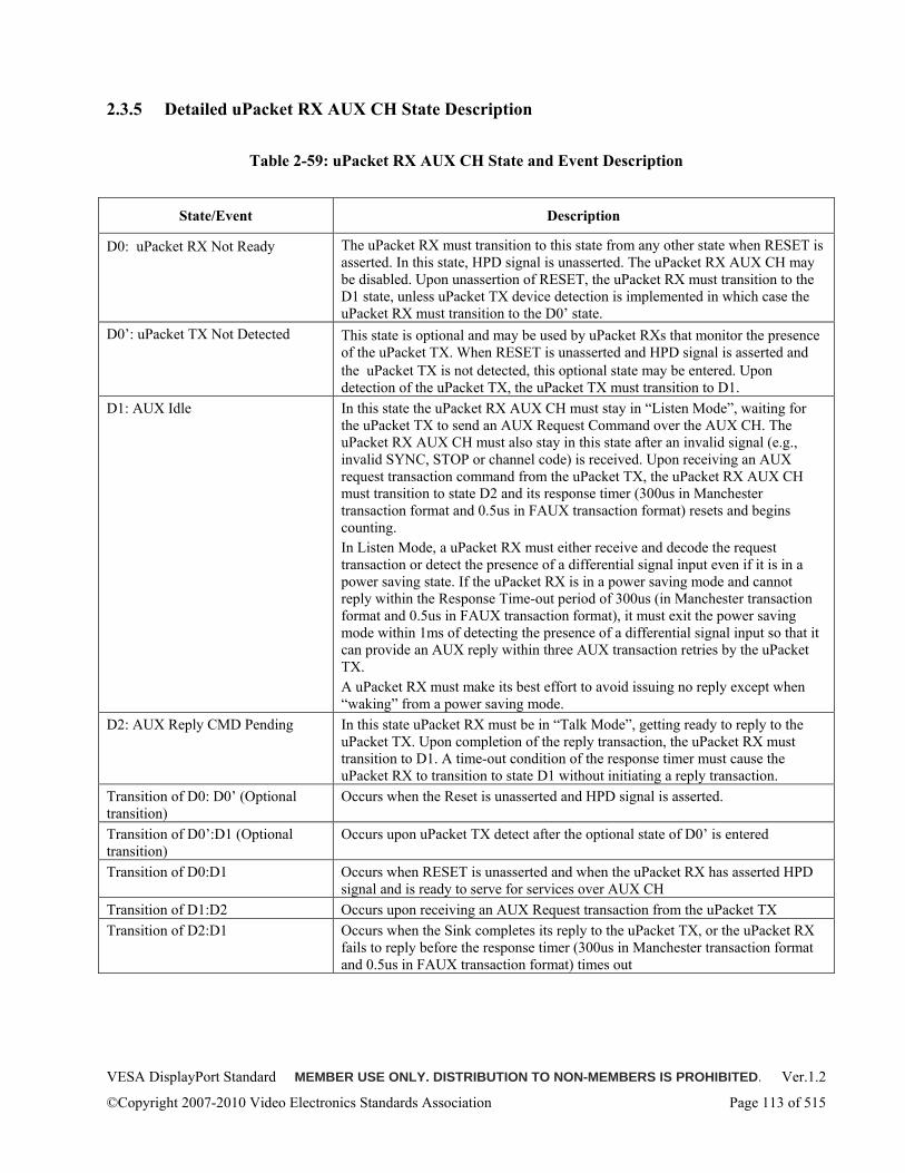
VESA DisplayPort Standard MEMBER USE ONLY. DISTRIBUTION TO NON-MEMBERS IS PROHIBITED. Ver.1.2
©Copyright 2007-2010 Video Electronics Standards Association Page 113 of 515
2.3.5 Detailed uPacket RX AUX CH State Description
Table 2-59: uPacket RX AUX CH State and Event Description
State/Event Description
D0: uPacket RX Not Ready The uPacket RX must transition to this state from any other state when RESET is asserted. In this state, HPD signal is unasserted. The uPacket RX AUX CH may be disabled. Upon unassertion of RESET, the uPacket RX must transition to the D1 state, unless uPacket TX device detection is implemented in which case the uPacket RX must transition to the D0’ state.
D0’: uPacket TX Not Detected This state is optional and may be used by uPacket RXs that monitor the presence of the uPacket TX. When RESET is unasserted and HPD signal is asserted and the uPacket TX is not detected, this optional state may be entered. Upon detection of the uPacket TX, the uPacket TX must transition to D1.
D1: AUX Idle In this state the uPacket RX AUX CH must stay in “Listen Mode”, waiting for the uPacket TX to send an AUX Request Command over the AUX CH. The uPacket RX AUX CH must also stay in this state after an invalid signal (e.g., invalid SYNC, STOP or channel code) is received. Upon receiving an AUX request transaction command from the uPacket TX, the uPacket RX AUX CH must transition to state D2 and its response timer (300us in Manchester transaction format and 0.5us in FAUX transaction format) resets and begins counting. In Listen Mode, a uPacket RX must either receive and decode the request transaction or detect the presence of a differential signal input even if it is in a power saving state. If the uPacket RX is in a power saving mode and cannot reply within the Response Time-out period of 300us (in Manchester transaction format and 0.5us in FAUX transaction format), it must exit the power saving mode within 1ms of detecting the presence of a differential signal input so that it can provide an AUX reply within three AUX transaction retries by the uPacket TX. A uPacket RX must make its best effort to avoid issuing no reply except when “waking” from a power saving mode.
D2: AUX Reply CMD Pending In this state uPacket RX must be in “Talk Mode”, getting ready to reply to the uPacket TX. Upon completion of the reply transaction, the uPacket RX must transition to D1. A time-out condition of the response timer must cause the uPacket RX to transition to state D1 without initiating a reply transaction.
Transition of D0: D0’ (Optional transition)
Occurs when the Reset is unasserted and HPD signal is asserted.
Transition of D0’:D1 (Optional transition)
Occurs upon uPacket TX detect after the optional state of D0’ is entered
Transition of D0:D1 Occurs when RESET is unasserted and when the uPacket RX has asserted HPD signal and is ready to serve for services over AUX CH
Transition of D1:D2 Occurs upon receiving an AUX Request transaction from the uPacket TX Transition of D2:D1 Occurs when the Sink completes its reply to the uPacket TX, or the uPacket RX
fails to reply before the response timer (300us in Manchester transaction format and 0.5us in FAUX transaction format) times out
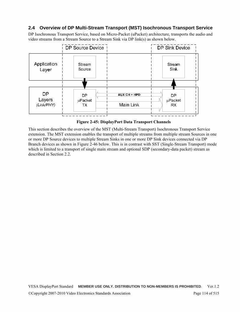
VESA DisplayPort Standard MEMBER USE ONLY. DISTRIBUTION TO NON-MEMBERS IS PROHIBITED. Ver.1.2
©Copyright 2007-2010 Video Electronics Standards Association Page 114 of 515
2.4 Overview of DP Multi-Stream Transport (MST) Isochronous Transport Service DP Isochronous Transport Service, based on Micro-Packet (uPacket) architecture, transports the audio and video streams from a Stream Source to a Stream Sink via DP link(s) as shown below.
Figure 2-45: DisplayPort Data Transport Channels
This section describes the overview of the MST (Multi-Stream Transport) Isochronous Transport Service extension. The MST extension enables the transport of multiple streams from multiple stream Sources in one or more DP Source devices to multiple Stream Sinks in one or more DP Sink devices connected via DP Branch devices as shown in Figure 2-46 below. This is in contrast with SST (Single-Stream Transport) mode which is limited to a transport of single main stream and optional SDP (secondary-data packet) stream as described in Section 2.2.
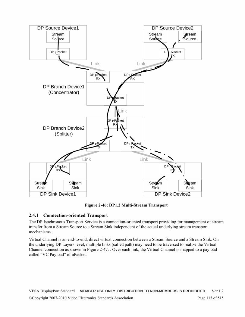
VESA DisplayPort Standard MEMBER USE ONLY. DISTRIBUTION TO NON-MEMBERS IS PROHIBITED. Ver.1.2
©Copyright 2007-2010 Video Electronics Standards Association Page 115 of 515
Stream Source
Stream Source
Stream Source
DP Packet TX
DP Packet TX
DP Packet TX
DP Packet RX
DP Packet RX
DP Packet RX
DP Packet TX
DP Packet TX
Stream Sink
DP Packet RX
Stream Sink
DP Packet RX
Stream Sink
Stream Sink
DP Source Device1 DP Source Device2
DP Sink Device1 DP Sink Device2
DP Branch Device1(Concentrator)
DP Branch Device2(Splitter)
Link Link
Link Link
Link
Figure 2-46: DP1.2 Multi-Stream Transport
2.4.1 Connection-oriented Transport The DP Isochronous Transport Service is a connection-oriented transport providing for management of stream transfer from a Stream Source to a Stream Sink independent of the actual underlying stream transport mechanisms.
Virtual Channel is an end-to-end, direct virtual connection between a Stream Source and a Stream Sink. On the underlying DP Layers level, multiple links (called path) may need to be traversed to realize the Virtual Channel connection as shown in Figure 2-47: . Over each link, the Virtual Channel is mapped to a payload called “VC Payload” of uPacket.
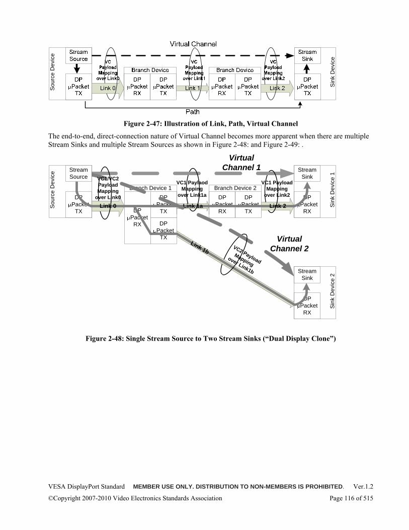
VESA DisplayPort Standard MEMBER USE ONLY. DISTRIBUTION TO NON-MEMBERS IS PROHIBITED. Ver.1.2
©Copyright 2007-2010 Video Electronics Standards Association Page 116 of 515
Sour
ce D
evic
e
Sin
k D
evic
e
Figure 2-47: Illustration of Link, Path, Virtual Channel
The end-to-end, direct-connection nature of Virtual Channel becomes more apparent when there are multiple Stream Sinks and multiple Stream Sources as shown in Figure 2-48: and Figure 2-49: .
DP Packet
TX
Stream Sink
Virtual Channel 1
DP PacketRX
DP Packet
TX
DP PacketRX
DP Packet
TX
Branch Device 1 Branch Device 2
Sou
rce
Dev
ice
Sin
k D
evic
e 1
DP PacketRX
Stream Sink
Sin
k D
evic
e 2
DP Packet
TX
DP PacketRX
Virtual Channel 2
Link 1b
Link 1a Link 2Link 0
VC2 Payload Mapping
over Link1b
VC1 Paylaod Mapping
over Link1a
VC1 PayloadMapping
over Link2
Stream Source VC1/VC2
Payload Mapping
over Link0
Figure 2-48: Single Stream Source to Two Stream Sinks (“Dual Display Clone”)
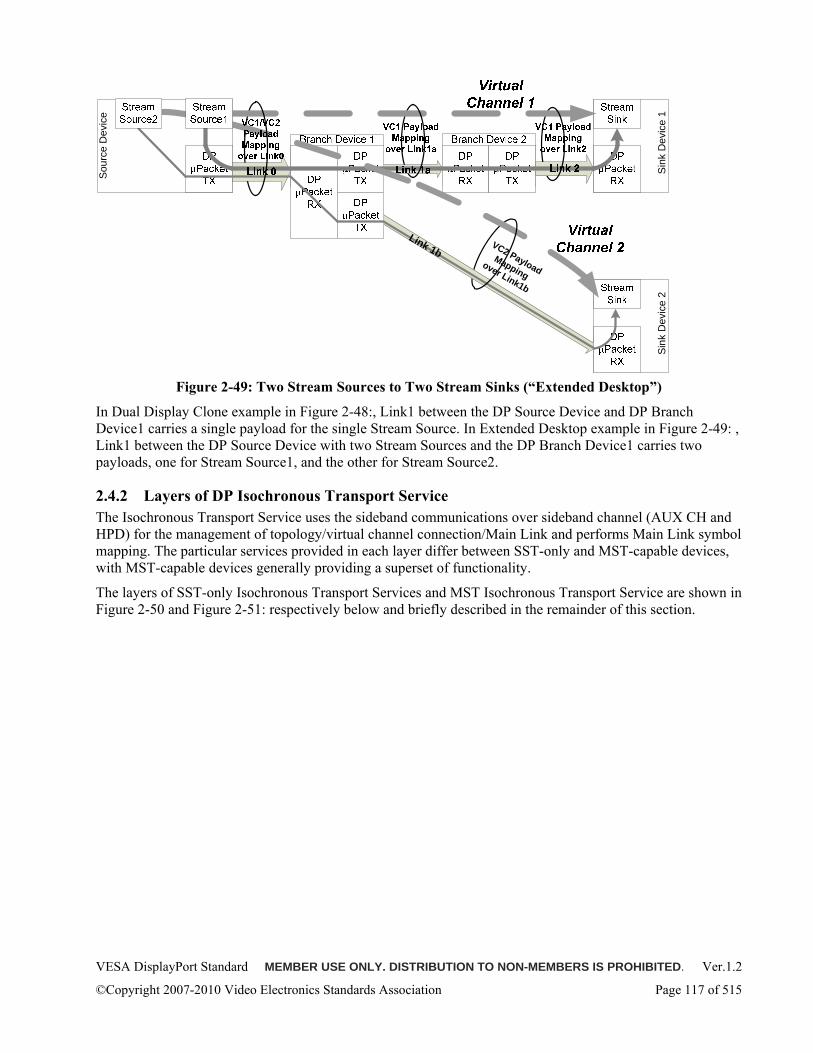
VESA DisplayPort Standard MEMBER USE ONLY. DISTRIBUTION TO NON-MEMBERS IS PROHIBITED. Ver.1.2
©Copyright 2007-2010 Video Electronics Standards Association Page 117 of 515
Sour
ce D
evic
e
Sin
k D
evic
e 1
Sink
Dev
ice
2
Link 1bVC2 Payload Mapping
over Link1b
Figure 2-49: Two Stream Sources to Two Stream Sinks (“Extended Desktop”)
In Dual Display Clone example in Figure 2-48:, Link1 between the DP Source Device and DP Branch Device1 carries a single payload for the single Stream Source. In Extended Desktop example in Figure 2-49: , Link1 between the DP Source Device with two Stream Sources and the DP Branch Device1 carries two payloads, one for Stream Source1, and the other for Stream Source2.
2.4.2 Layers of DP Isochronous Transport Service The Isochronous Transport Service uses the sideband communications over sideband channel (AUX CH and HPD) for the management of topology/virtual channel connection/Main Link and performs Main Link symbol mapping. The particular services provided in each layer differ between SST-only and MST-capable devices, with MST-capable devices generally providing a superset of functionality.
The layers of SST-only Isochronous Transport Services and MST Isochronous Transport Service are shown in Figure 2-50 and Figure 2-51: respectively below and briefly described in the remainder of this section.
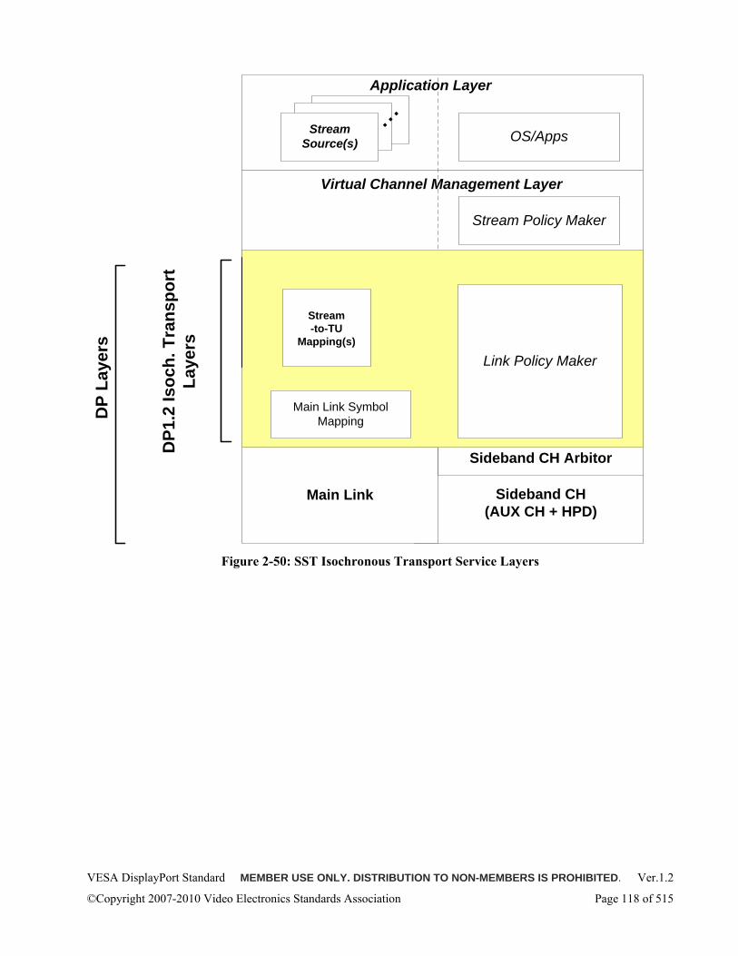
VESA DisplayPort Standard MEMBER USE ONLY. DISTRIBUTION TO NON-MEMBERS IS PROHIBITED. Ver.1.2
©Copyright 2007-2010 Video Electronics Standards Association Page 118 of 515
Virtual Channel Management Layer
Application Layer
OS/Apps
Stream Policy Maker
Stream Source(s)
DP
Laye
rs
Main Link
DP1
.2 Is
och.
Tra
nspo
rt
Laye
rs
Sideband CH(AUX CH + HPD)
Sideband CH Arbitor
Link Policy Maker
Main Link Symbol Mapping
Stream-to-TU
Mapping(s)
Figure 2-50: SST Isochronous Transport Service Layers
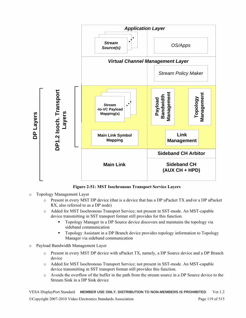
VESA DisplayPort Standard MEMBER USE ONLY. DISTRIBUTION TO NON-MEMBERS IS PROHIBITED. Ver.1.2
©Copyright 2007-2010 Video Electronics Standards Association Page 119 of 515
Virtual Channel Management Layer
Application Layer
OS/Apps
Stream Policy Maker
Stream Source(s)
Link Management
Main Link Symbol MappingD
P La
yers
Main Link
DP1
.2 Is
och.
Tra
nspo
rt
Laye
rs
Stream-to-VC Payload
Mapping(s)
Sideband CH(AUX CH + HPD)
Sideband CH Arbitor
Topo
logy
M
anag
emen
t
Payl
oad
Ban
dwid
th
Man
agem
ent
Figure 2-51: MST Isochronous Transport Service Layers
o Topology Management Layer o Present in every MST DP device (that is a device that has a DP uPacket TX and/or a DP uPacket
RX, also referred to as a DP node) o Added for MST Isochronous Transport Service; not present in SST-mode. An MST-capable
device transmitting in SST transport format still provides for this function. Topology Manager in a DP Source device discovers and maintains the topology via
sideband communication Topology Assistant in a DP Branch device provides topology information to Topology
Manager via sideband communication
o Payload Bandwidth Management Layer
o Present in every MST DP device with uPacket TX, namely, a DP Source device and a DP Branch device
o Added for MST Isochronous Transport Service; not present in SST-mode. An MST-capable device transmitting in SST transport format still provides this function.
o Avoids the overflow of the buffer in the path from the stream source in a DP Source device to the Stream Sink in a DP Sink device
VESA DisplayPort Standard MEMBER USE ONLY. DISTRIBUTION TO NON-MEMBERS IS PROHIBITED. Ver.1.2
©Copyright 2007-2010 Video Electronics Standards Association Page 120 of 515
Source Payload Bandwidth Manager in a DP Source device receives the stream bandwidth, calculates Payload Bandwidth Number (PBN) corresponding to the stream bandwidth, forwards the PBN value via sideband communication, and sets the VC Payload Bandwidth of its own downstream link by allocating sufficient time slots to the VC Payload.
Branch Payload Bandwidth Manager in a DP Branch device receives and forwards the PBN via sideband communication, and sets the VC Payload Bandwidth of its own downstream link by allocating sufficient time slots to the VC Payload.
Instructs Main Link Symbol Mapping Layer how many time slots to allocate to a VC Payload Allocation and when to enable/disable insertion of Stream Symbols from VC Payload Mapping Layer into a VC Payload.
o Link Management Layer
o Present in every MST DP uPacket TX and DP uPacket RX o Present both in MST and SST modes (referred to as Link Policy Maker in SST-only devices) o Establishes and maintains Main Link through Link Training and Link Maintenance
Link Management Layer of uPacket TX instructs Main Link Symbol Mapping Layer to transmit Link Training Patterns and, once Link Training is successful, to transmit uPackets (called Multi-stream Transport Packet, or MTP) to keep the link enabled; also monitors the status of the uPacket RX it is driving.
Link Management Layer of uPacket RX provides for ADJUST_REQUEST for uPacket TX drive setting optimization during Link Training, and keeps the link status information up to date, generating IRQ_HPD pulse when it requires the attention of Link Management Layer of the uPacket TX.
o Main Link Symbol Mapping Layer
o Present in every uPacket TX and uPacket RX o Enhanced for MST Isochronous Transport Service
Main Link Symbol Mapping Layer of uPacket TX transmits Link Training Patterns and MTP Symbols as instructed by the Link Management Layer; also allocates time slots to a VC Payload and controls the insertion of Stream Symbols coming from the VC Payload Mapping Layer as instructed by the Payload Bandwidth Management Layer.
Main Link Symbol Mapping Layer of uPacket RX receives Main Link Symbols and informs its Link Management Layer of the link quality; also keeps VC Payload allocation synchronized with that of uPacket TX of the immediate upstream DP device and extracts Stream Symbols from incoming MTP Symbols.
o VC Payload Mapping Layer
o Present per stream o Present both in MST mode and SST mode (Stream-to-TU Payload Mapping Layer)
VC Payload Mapping Layer in a DP Source device receives stream (both data and control) from a stream source and converts it to Stream Symbols inserted into VC Payload.
VC Payload Mapping Layer in a DP Sink device regenerates the stream from incoming Stream Symbols.
VC Payload Mapping Layer in a DP Branch device passes through incoming Stream Symbols from its upstream uPacket RX to its downstream uPacket TX in a manner that is agnostic to stream data format/symbol type/lane count (that is, no symbol parsing needed)
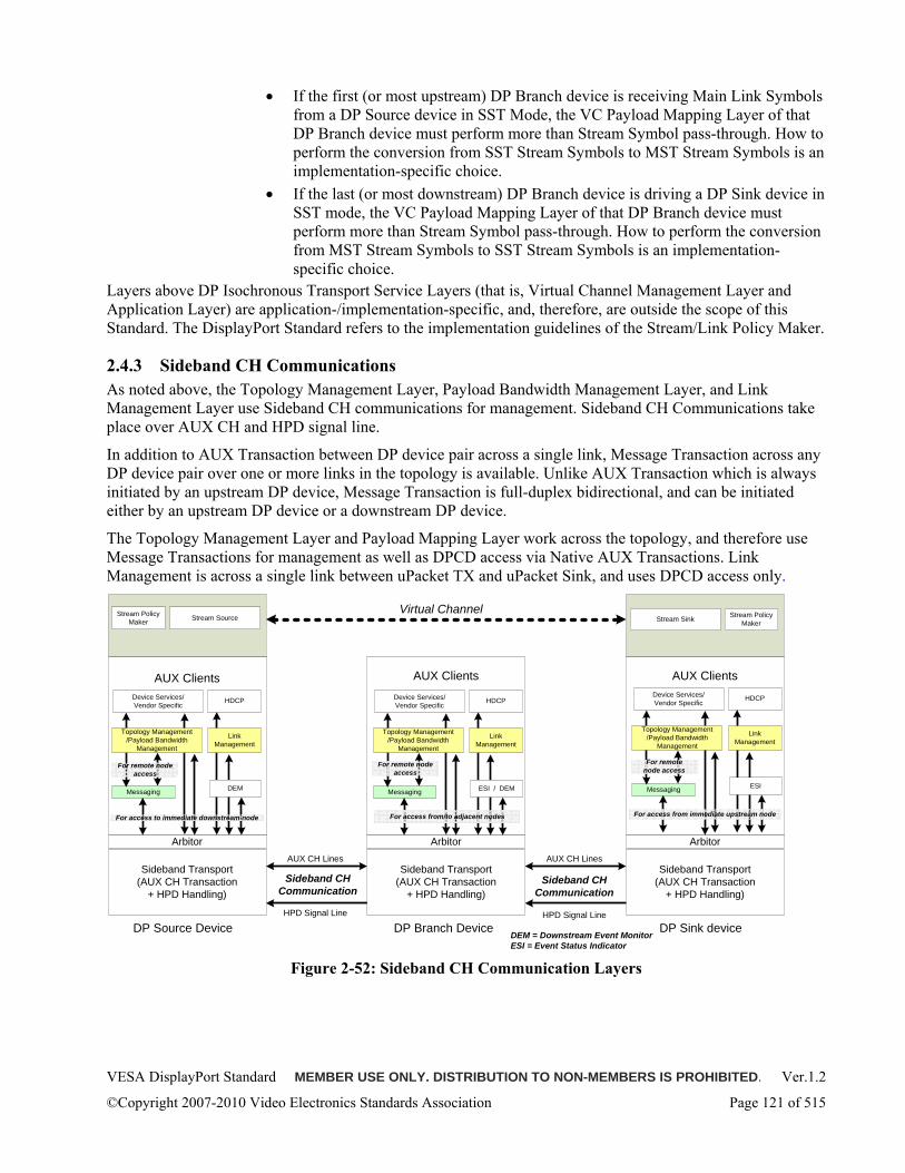
VESA DisplayPort Standard MEMBER USE ONLY. DISTRIBUTION TO NON-MEMBERS IS PROHIBITED. Ver.1.2
©Copyright 2007-2010 Video Electronics Standards Association Page 121 of 515
• If the first (or most upstream) DP Branch device is receiving Main Link Symbols from a DP Source device in SST Mode, the VC Payload Mapping Layer of that DP Branch device must perform more than Stream Symbol pass-through. How to perform the conversion from SST Stream Symbols to MST Stream Symbols is an implementation-specific choice.
• If the last (or most downstream) DP Branch device is driving a DP Sink device in SST mode, the VC Payload Mapping Layer of that DP Branch device must perform more than Stream Symbol pass-through. How to perform the conversion from MST Stream Symbols to SST Stream Symbols is an implementation-specific choice.
Layers above DP Isochronous Transport Service Layers (that is, Virtual Channel Management Layer and Application Layer) are application-/implementation-specific, and, therefore, are outside the scope of this Standard. The DisplayPort Standard refers to the implementation guidelines of the Stream/Link Policy Maker.
2.4.3 Sideband CH Communications As noted above, the Topology Management Layer, Payload Bandwidth Management Layer, and Link Management Layer use Sideband CH communications for management. Sideband CH Communications take place over AUX CH and HPD signal line.
In addition to AUX Transaction between DP device pair across a single link, Message Transaction across any DP device pair over one or more links in the topology is available. Unlike AUX Transaction which is always initiated by an upstream DP device, Message Transaction is full-duplex bidirectional, and can be initiated either by an upstream DP device or a downstream DP device.
The Topology Management Layer and Payload Mapping Layer work across the topology, and therefore use Message Transactions for management as well as DPCD access via Native AUX Transactions. Link Management is across a single link between uPacket TX and uPacket Sink, and uses DPCD access only.
Sideband CH Communication
AUX CH Lines
HPD Signal Line
DP Source Device DP Sink device
Sideband Transport(AUX CH Transaction
+ HPD Handling)
Arbitor
AUX Clients
AUX CH Lines
HPD Signal LineDP Branch Device
Sideband CH Communication
Sideband Transport(AUX CH Transaction
+ HPD Handling)
Arbitor
Device Services/Vendor Specific
HDCP
AUX Clients
Messaging
Topology Management/Payload Bandwidth
Management
Link Management
DEM
Sideband Transport(AUX CH Transaction
+ HPD Handling)
Arbitor
AUX Clients
Virtual ChannelStream SourceStream Policy
MakerStream Policy
MakerStream Sink
Device Services/Vendor Specific
HDCP
Messaging
Topology Management/Payload Bandwidth
Management
Link Management
ESI / DEM
For remote node access
Device Services/Vendor Specific
HDCP
Messaging
Topology Management/Payload Bandwidth
Management
Link Management
ESI
For remote node access
For access from/to adjacent nodesFor access to immediate downstream node For access from immediate upstream node
For remote node access
DEM = Downstream Event MonitorESI = Event Status Indicator
Figure 2-52: Sideband CH Communication Layers
VESA DisplayPort Standard MEMBER USE ONLY. DISTRIBUTION TO NON-MEMBERS IS PROHIBITED. Ver.1.2
©Copyright 2007-2010 Video Electronics Standards Association Page 122 of 515
2.5 Topology Management Layer Topology Management layer using Messaging AUX Client, covered in Section 2.11 of this document, helps the Topology Manager in a DP Source device (optional in a DP Sink device) determine what devices are in the topology.
This section consists of the following subsections.
o Primitives of MST DP Devices and Device Types (Section 2.5.1) o Primitives of the MST DP devices are a uPacket TX, a uPacket RX, a branching unit, a stream
source, and a stream sink. MST DP Branch, Source, Sink, and Composite devices are comprised of various combinations of these primitives.
o MST Topologies (Section 2.5.2) o DP Branch devices of MST topology need to be MST devices supporting Topology Management
while the “end” device (DP Source, DP Sink, and Converter device) may be either MST or SST device.
o MST Device Identification (Section 2.5.3) o MST device with a branching unit is identified with Globally Unique Identifier (GUID) and
Relative Address (RAD). The end device that has no branching unit is identified as a “peer device” connected to one of the ports of the MST device with a branching unit. A DP device with uPacket RX with DPCD Revision number 1.2 or higher must have GUID field at DPCD Addresses 00030h ~ 0003Fh.
o Topology Manager and Topology Assistant (Section 2.5.4) o Topology Management is conducted through the collaboration between Topology Manager in
MST DP Source device (optionally in MST DP Sink device) and Topology Assistant in MST device with a branching unit.
o Topology Discovery (Section 2.5.5) o Topology Manager obtains information about the topology by using Native AUX transactions and
Messaging AUX Client, namely, LINK_ADDRESS Message Transaction. (Messaging AUX Client is covered in Section 2.11. The amount of information obtained about the topology and the use of the information is Topology Manager implementation-specific.
o Topology Maintenance (Section 2.5.6) o Topology Manager receives notifications when DP devices and legacy devices are connected and
disconnected from the topology. These notifications are provided by Topology Assistants via Messaging AUX Client, namely, CONNECTION_STATUS_NOTIFY Message Transaction.
o Topologies with SST-only Source devices (Section 2.5.7) o Topology option with SST Source Device is restricted.
o Loop Handling (Section 2.5.8) o MST Topology Management feature provides for enough information for Topology Manager to
properly handle a topology with a loop and/or a parallel path.
2.5.1 Primitives of MST DP Devices and Device Types Primitives of DP devices are a uPacket TX, a uPacket RX, a branching unit, a stream source, and a stream sink.
The branching unit must meet the following requirements:
o Must have both input and output ports and be capable of VC Payload routing from the input ports to the output ports.
o Must have at least one input port and one output port.
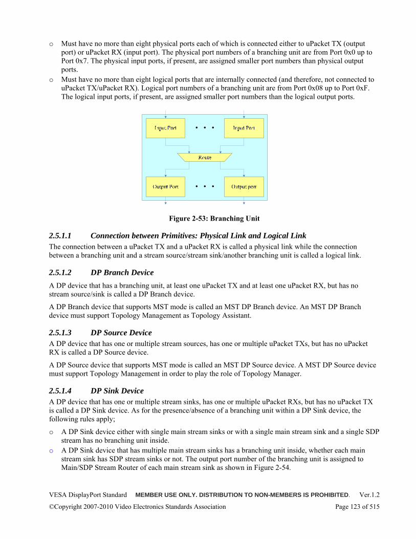
VESA DisplayPort Standard MEMBER USE ONLY. DISTRIBUTION TO NON-MEMBERS IS PROHIBITED. Ver.1.2
©Copyright 2007-2010 Video Electronics Standards Association Page 123 of 515
o Must have no more than eight physical ports each of which is connected either to uPacket TX (output port) or uPacket RX (input port). The physical port numbers of a branching unit are from Port 0x0 up to Port 0x7. The physical input ports, if present, are assigned smaller port numbers than physical output ports.
o Must have no more than eight logical ports that are internally connected (and therefore, not connected to uPacket TX/uPacket RX). Logical port numbers of a branching unit are from Port 0x08 up to Port 0xF. The logical input ports, if present, are assigned smaller port numbers than the logical output ports.
Figure 2-53: Branching Unit
2.5.1.1 Connection between Primitives: Physical Link and Logical Link The connection between a uPacket TX and a uPacket RX is called a physical link while the connection between a branching unit and a stream source/stream sink/another branching unit is called a logical link.
2.5.1.2 DP Branch Device A DP device that has a branching unit, at least one uPacket TX and at least one uPacket RX, but has no stream source/sink is called a DP Branch device.
A DP Branch device that supports MST mode is called an MST DP Branch device. An MST DP Branch device must support Topology Management as Topology Assistant.
2.5.1.3 DP Source Device A DP device that has one or multiple stream sources, has one or multiple uPacket TXs, but has no uPacket RX is called a DP Source device.
A DP Source device that supports MST mode is called an MST DP Source device. A MST DP Source device must support Topology Management in order to play the role of Topology Manager.
2.5.1.4 DP Sink Device A DP device that has one or multiple stream sinks, has one or multiple uPacket RXs, but has no uPacket TX is called a DP Sink device. As for the presence/absence of a branching unit within a DP Sink device, the following rules apply;
o A DP Sink device either with single main stream sinks or with a single main stream sink and a single SDP stream has no branching unit inside.
o A DP Sink device that has multiple main stream sinks has a branching unit inside, whether each main stream sink has SDP stream sinks or not. The output port number of the branching unit is assigned to Main/SDP Stream Router of each main stream sink as shown in Figure 2-54.
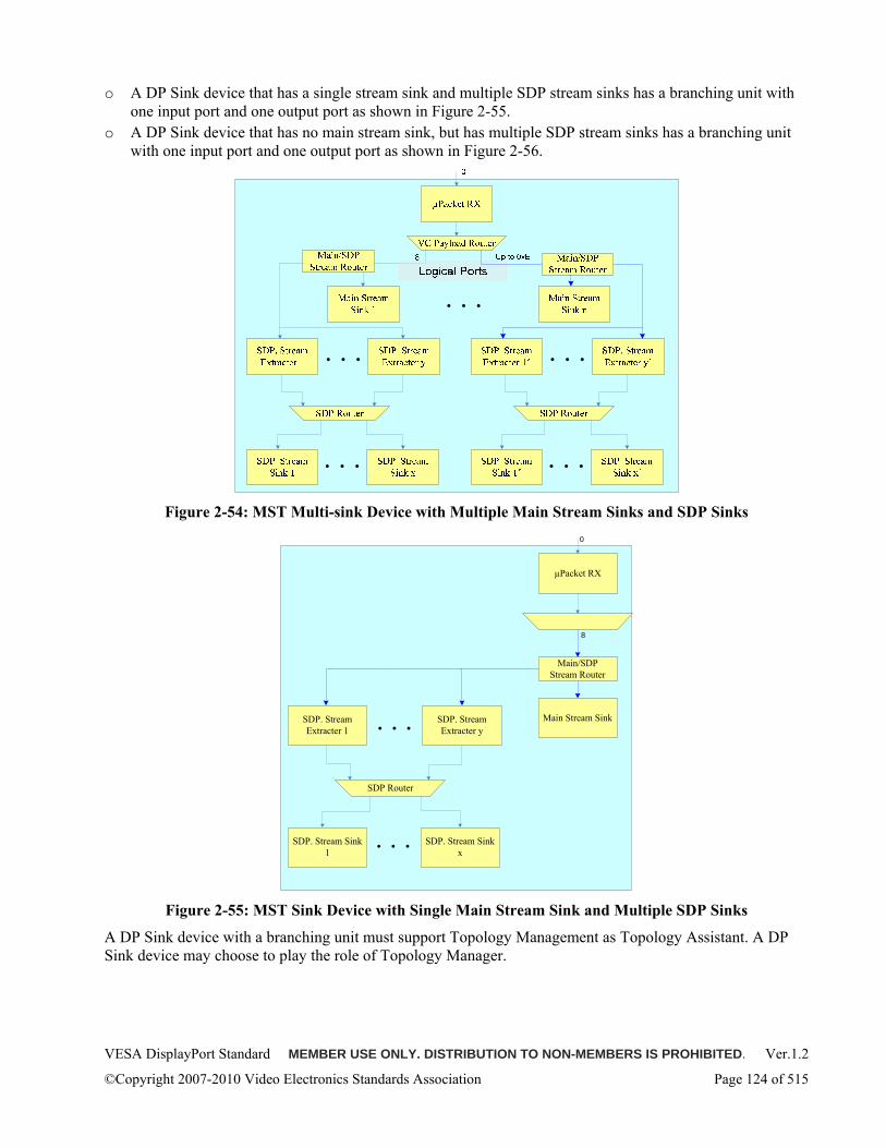
VESA DisplayPort Standard MEMBER USE ONLY. DISTRIBUTION TO NON-MEMBERS IS PROHIBITED. Ver.1.2
©Copyright 2007-2010 Video Electronics Standards Association Page 124 of 515
o A DP Sink device that has a single stream sink and multiple SDP stream sinks has a branching unit with one input port and one output port as shown in Figure 2-55.
o A DP Sink device that has no main stream sink, but has multiple SDP stream sinks has a branching unit with one input port and one output port as shown in Figure 2-56.
Figure 2-54: MST Multi-sink Device with Multiple Main Stream Sinks and SDP Sinks
µPacket RX
0
SDP. Stream Extracter 1
SDP. Stream Extracter y
SDP. Stream Sink 1
SDP Router
SDP. Stream Sink x
Main/SDP Stream Router
Main Stream Sink
8
Figure 2-55: MST Sink Device with Single Main Stream Sink and Multiple SDP Sinks
A DP Sink device with a branching unit must support Topology Management as Topology Assistant. A DP Sink device may choose to play the role of Topology Manager.
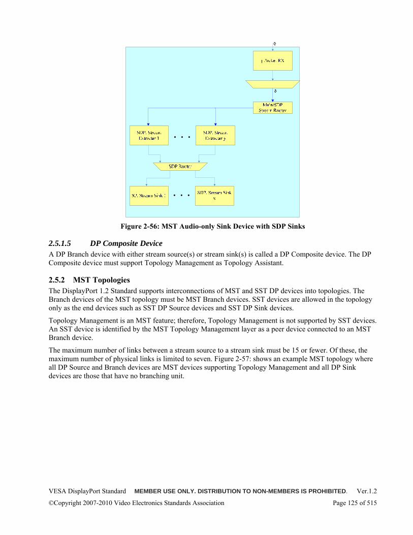
VESA DisplayPort Standard MEMBER USE ONLY. DISTRIBUTION TO NON-MEMBERS IS PROHIBITED. Ver.1.2
©Copyright 2007-2010 Video Electronics Standards Association Page 125 of 515
Figure 2-56: MST Audio-only Sink Device with SDP Sinks
2.5.1.5 DP Composite Device A DP Branch device with either stream source(s) or stream sink(s) is called a DP Composite device. The DP Composite device must support Topology Management as Topology Assistant.
2.5.2 MST Topologies The DisplayPort 1.2 Standard supports interconnections of MST and SST DP devices into topologies. The Branch devices of the MST topology must be MST Branch devices. SST devices are allowed in the topology only as the end devices such as SST DP Source devices and SST DP Sink devices.
Topology Management is an MST feature; therefore, Topology Management is not supported by SST devices. An SST device is identified by the MST Topology Management layer as a peer device connected to an MST Branch device.
The maximum number of links between a stream source to a stream sink must be 15 or fewer. Of these, the maximum number of physical links is limited to seven. Figure 2-57: shows an example MST topology where all DP Source and Branch devices are MST devices supporting Topology Management and all DP Sink devices are those that have no branching unit.
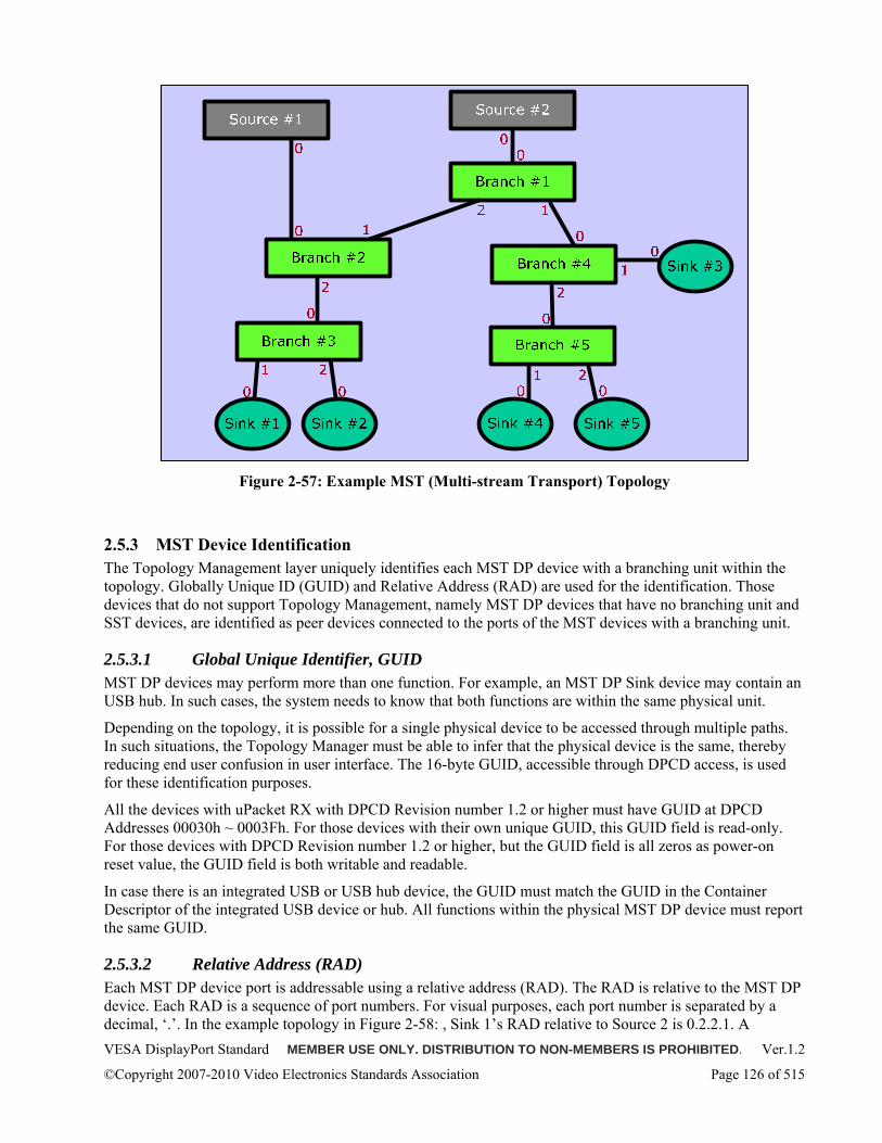
VESA DisplayPort Standard MEMBER USE ONLY. DISTRIBUTION TO NON-MEMBERS IS PROHIBITED. Ver.1.2
©Copyright 2007-2010 Video Electronics Standards Association Page 126 of 515
Figure 2-57: Example MST (Multi-stream Transport) Topology
2.5.3 MST Device Identification The Topology Management layer uniquely identifies each MST DP device with a branching unit within the topology. Globally Unique ID (GUID) and Relative Address (RAD) are used for the identification. Those devices that do not support Topology Management, namely MST DP devices that have no branching unit and SST devices, are identified as peer devices connected to the ports of the MST devices with a branching unit.
2.5.3.1 Global Unique Identifier, GUID MST DP devices may perform more than one function. For example, an MST DP Sink device may contain an USB hub. In such cases, the system needs to know that both functions are within the same physical unit.
Depending on the topology, it is possible for a single physical device to be accessed through multiple paths. In such situations, the Topology Manager must be able to infer that the physical device is the same, thereby reducing end user confusion in user interface. The 16-byte GUID, accessible through DPCD access, is used for these identification purposes.
All the devices with uPacket RX with DPCD Revision number 1.2 or higher must have GUID at DPCD Addresses 00030h ~ 0003Fh. For those devices with their own unique GUID, this GUID field is read-only. For those devices with DPCD Revision number 1.2 or higher, but the GUID field is all zeros as power-on reset value, the GUID field is both writable and readable.
In case there is an integrated USB or USB hub device, the GUID must match the GUID in the Container Descriptor of the integrated USB device or hub. All functions within the physical MST DP device must report the same GUID.
2.5.3.2 Relative Address (RAD) Each MST DP device port is addressable using a relative address (RAD). The RAD is relative to the MST DP device. Each RAD is a sequence of port numbers. For visual purposes, each port number is separated by a decimal, ‘.’. In the example topology in Figure 2-58: , Sink 1’s RAD relative to Source 2 is 0.2.2.1. A
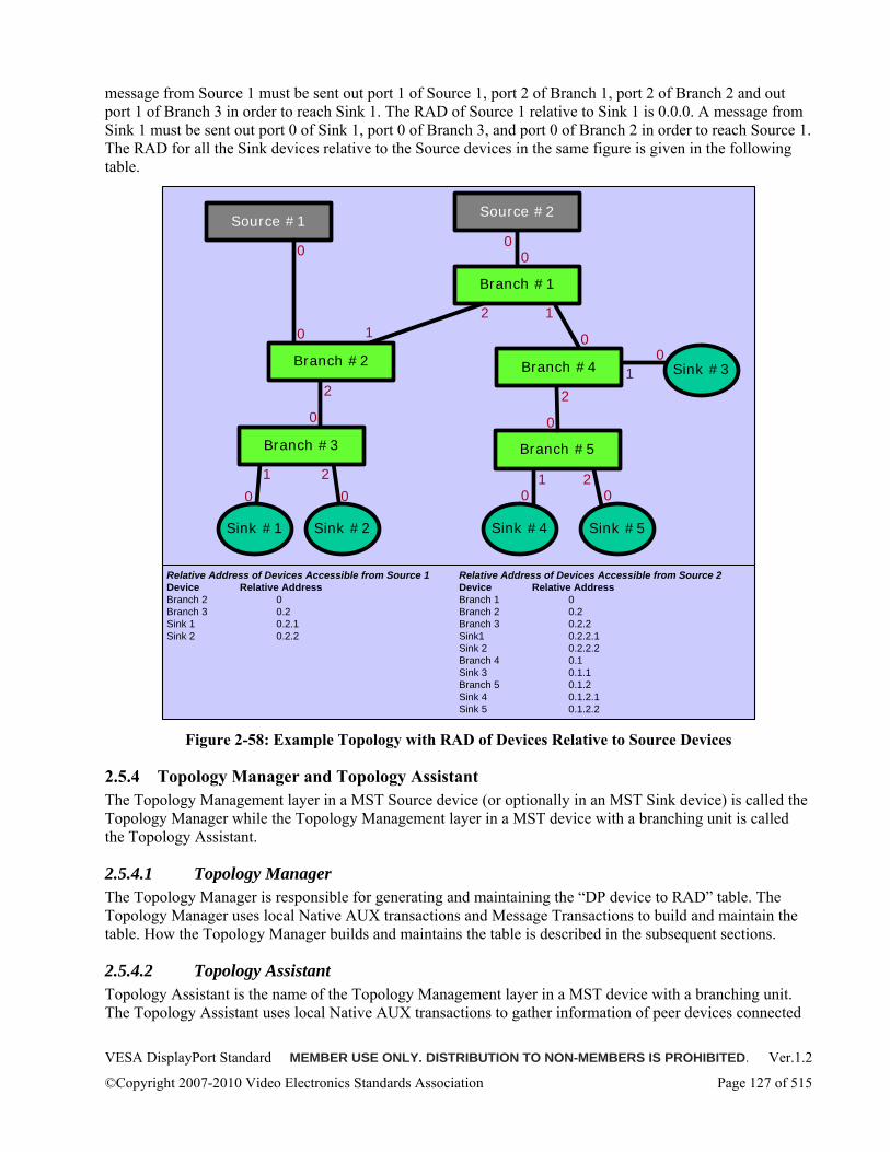
VESA DisplayPort Standard MEMBER USE ONLY. DISTRIBUTION TO NON-MEMBERS IS PROHIBITED. Ver.1.2
©Copyright 2007-2010 Video Electronics Standards Association Page 127 of 515
message from Source 1 must be sent out port 1 of Source 1, port 2 of Branch 1, port 2 of Branch 2 and out port 1 of Branch 3 in order to reach Sink 1. The RAD of Source 1 relative to Sink 1 is 0.0.0. A message from Sink 1 must be sent out port 0 of Sink 1, port 0 of Branch 3, and port 0 of Branch 2 in order to reach Source 1. The RAD for all the Sink devices relative to the Source devices in the same figure is given in the following table.
Relative Address of Devices Accessible from Source 1 Relative Address of Devices Accessible from Source 2Device Relative Address Device Relative AddressBranch 2 0 Branch 1 0Branch 3 0.2 Branch 2 0.2Sink 1 0.2.1 Branch 3 0.2.2Sink 2 0.2.2 Sink1 0.2.2.1
Sink 2 0.2.2.2Branch 4 0.1Sink 3 0.1.1Branch 5 0.1.2Sink 4 0.1.2.1Sink 5 0.1.2.2
Branch #5
Source #2Source #1
Branch #1
Branch #4
Sink #1 Sink #2 Sink #4 Sink #5
Sink #3Branch #2
12
0
1
2
0 1
2
0
21
0
1 2
00
0
Branch #3
00
0
00
Figure 2-58: Example Topology with RAD of Devices Relative to Source Devices
2.5.4 Topology Manager and Topology Assistant The Topology Management layer in a MST Source device (or optionally in an MST Sink device) is called the Topology Manager while the Topology Management layer in a MST device with a branching unit is called the Topology Assistant.
2.5.4.1 Topology Manager The Topology Manager is responsible for generating and maintaining the “DP device to RAD” table. The Topology Manager uses local Native AUX transactions and Message Transactions to build and maintain the table. How the Topology Manager builds and maintains the table is described in the subsequent sections.
2.5.4.2 Topology Assistant Topology Assistant is the name of the Topology Management layer in a MST device with a branching unit. The Topology Assistant uses local Native AUX transactions to gather information of peer devices connected
VESA DisplayPort Standard MEMBER USE ONLY. DISTRIBUTION TO NON-MEMBERS IS PROHIBITED. Ver.1.2
©Copyright 2007-2010 Video Electronics Standards Association Page 128 of 515
to it and provides for the information as requested by the Topology Manager. The information provided by Topology Assistants is described later in this section.
2.5.5 Topology Discovery The goal of Topology Discovery is stream policy maker implementation-specific. The goal may be to find the closest DP Sink device; build a DP Sink device to RAD table; or graphically display the topology showing each device and its associated interconnections.
2.5.5.1 Topology Manager The Topology Manager uses Native AUX transactions and Message Transactions to implement its Topology Discovery algorithm. Upon power up, the Topology Manager monitors the connection status of its local downstream ports via the HPD signal of each port. When a device is connected to one of its DP ports, the Topology Manager reads the capabilities of the immediate downstream DisplayPort device using Native AUX transactions. The device capabilities include the device type and whether Messaging is supported. If the connected device (that is, the peer device) is an MST device with a branching unit, the Topology Manager can instruct the Messaging AUX Client to send a LINK_ADDRESS message transaction request to the device to determine the device Global Unique Identifier, GUID, the number of input and output ports and the type and capabilities of devices connected to the device’s input and output ports (called Peer_Device Types). The Topology Manager, using the information obtained from the LINK_ADDRESS message transaction response, can further send LINK_ADDRESS messages to other MST DP devices containing branching units until the goal of its Topology Discovery is met.
2.5.5.2 Topology Assistant The responsibility of the Topology Assistant in an MST device with a branching unit during the Topology Discovery procedure is to reply to the LINK_ADDRESS Request Message Transaction with its capabilities and the Peer Device Type of each DP device connected to its DP uPacket TX and RX ports (either physical or logical).The Topology Manager gathers the information of the peer devices using Native AUX transactions.
2.5.6 Topology Maintenance Topology Maintenance is the continual monitoring for DP device connection or removal from the topology. The Topology Assistant within each MST DP Branch/Composite device is responsible for detecting and notifying the Topology Managers when devices are connected or removed. What the Topology Manager does with this notification is implementation-specific.
2.5.6.1 Topology Manager During Topology Maintenance, the Topology Manager may receive CONNECTION_STATUS_NOTIFY Broadcast Request Message Transactions when MST DP Branch devices are connected to or disconnected from the topology. The following information is provided with the CONNECTION_STATUS_NOTIFY Broadcast Request Message Transaction: the GUID of the MST device where the connection change was detected; the port number on the device and whether the port is an input or output where the connection change was detected; the new connection status for the port where the connection change was detected; the peer device type if a new DP device was connected; and whether the newly connected DP device supports Messaging. How the Topology Manager uses this information is implementation-specific. The notification may be ignored if not required.
2.5.6.2 Topology Assistant Once an MST DP device with a branching unit powers on, it continually monitors the connection status of each of its input and output ports using the connection mechanism associated with the corresponding port type, HPD for DP uPacket TX ports and cable termination for DP uPacket RX ports. All internal DP Sinks of a logical branch device are connected by default. When the connection status of any DP port changes, the new
VESA DisplayPort Standard MEMBER USE ONLY. DISTRIBUTION TO NON-MEMBERS IS PROHIBITED. Ver.1.2
©Copyright 2007-2010 Video Electronics Standards Association Page 129 of 515
status is broadcast out to all connected DP uPacket TX and RX ports using the CONNECTION_STATUS_NOTIFY Broadcast Message Transaction request. The Topology Assistant continues monitoring its DP uPacket TX and RX ports for connection changes. The Topology Assistant may receive one or more LINK_ADDRESS Message Transaction requests. Each LINK_ADDRESS request will be handled the same as during the Topology Discovery procedure.
2.5.7 Topologies with SST-only Source devices When a topology contains one or more SST-only DP Source devices, the MST DP Branch device connected to the SST-only DP Source devices must perform the SST-only Topology Management function. The MST DP Branch device recognizes the upstream device as the SST-only device when the upstream device keeps UP_REQ_EN bit cleared to 0. An MST upstream device may act and be treated as an SST-only device by not setting UP_REQ_EN bit to 1.
The SST-only Topology Management function is a basic input to output port selection. The MST DP Branch device connected to an SST-only Source device acts as an SST-only Branch device as described in Section 5.3. An MST Branch device acting as an SST-only Branch device must not perform SST input to MST output conversion.
A uPacket TX of an MST DP Source device may choose to transmit in SST transport format (that is, keeps MST_EN bit of the downstream device cleared to 0) while setting the UP_REQ_EN bit to 1, as long as it performs the role of Topology Manager and Source Payload Bandwidth Manager and originates Message Transactions for virtual channel management prior to SST stream transmission. Once the MST DP Source device establishes the virtual channel via Message Transactions and transmits in SST transport format, the MST DP Branch device must convert the SST input into MST output.
2.5.8 Loop Handling While DP MST topologies should be constructed without loops or parallel paths, the Topology Manager must be able to handle the case where loops or parallel paths exist.
The GUID obtained from the LINK_ADDRESS Message Transaction request and the RAD of the DP device queried provide for enough information to determine whether a loop or parallel path in the topology exists. The path chosen to access a DP device accessible through multiple paths is Topology Manager implementation-specific, including the handling of a topology that has a loop and/or a parallel path. An example topology with a loop and parallel path is shown in Figure 2-59 along with the GUID and RAD for the loop and parallel path.
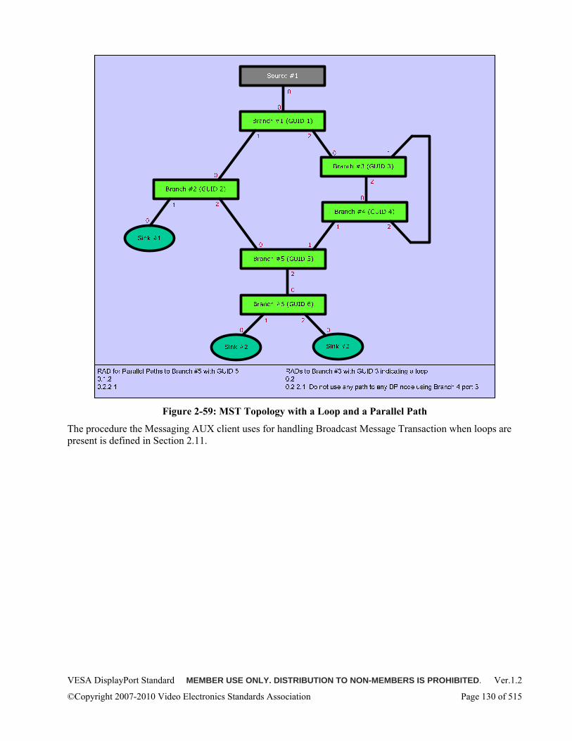
VESA DisplayPort Standard MEMBER USE ONLY. DISTRIBUTION TO NON-MEMBERS IS PROHIBITED. Ver.1.2
©Copyright 2007-2010 Video Electronics Standards Association Page 130 of 515
Figure 2-59: MST Topology with a Loop and a Parallel Path
The procedure the Messaging AUX client uses for handling Broadcast Message Transaction when loops are present is defined in Section 2.11.
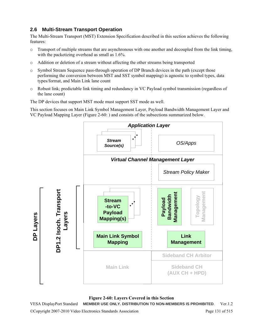
VESA DisplayPort Standard MEMBER USE ONLY. DISTRIBUTION TO NON-MEMBERS IS PROHIBITED. Ver.1.2
©Copyright 2007-2010 Video Electronics Standards Association Page 131 of 515
2.6 Multi-Stream Transport Operation The Multi-Stream Transport (MST) Extension Specification described in this section achieves the following features:
o Transport of multiple streams that are asynchronous with one another and decoupled from the link timing, with the packetizing overhead as small as 1.6%.
o Addition or deletion of a stream without affecting the other streams being transported
o Symbol Stream Sequence pass-through operation of DP Branch devices in the path (except those performing the conversion between MST and SST symbol mapping) is agnostic to symbol types, data types/format, and Main Link lane count
o Robust link; predictable link timing and redundancy in VC Payload symbol transmission (regardless of the lane count)
The DP devices that support MST mode must support SST mode as well.
This section focuses on Main Link Symbol Management Layer, Payload Bandwidth Management Layer and VC Payload Mapping Layer (Figure 2-60: ) and consists of the subsections summarized below.
Virtual Channel Management Layer
Application Layer
OS/Apps
Stream Policy Maker
Topo
logy
M
anag
emen
t
Stream Source(s)
Link Management
Main Link Symbol MappingD
P La
yers
Main Link
DP1
.2 Is
och.
Tra
nspo
rt
Laye
rs
Stream-to-VC
Payload Mapping(s)
Payl
oad
Ban
dwid
th
Man
agem
ent
Sideband CH(AUX CH + HPD)
Sideband CH Arbitor
Figure 2-60: Layers Covered in this Section
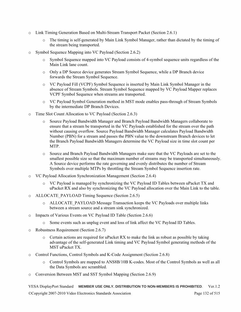
VESA DisplayPort Standard MEMBER USE ONLY. DISTRIBUTION TO NON-MEMBERS IS PROHIBITED. Ver.1.2
©Copyright 2007-2010 Video Electronics Standards Association Page 132 of 515
o Link Timing Generation Based on Multi-Stream Transport Packet (Section 2.6.1)
o The timing is self-generated by Main Link Symbol Manager, rather than dictated by the timing of the stream being transported.
o Symbol Sequence Mapping into VC Payload (Section 2.6.2)
o Symbol Sequence mapped into VC Payload consists of 4-symbol sequence units regardless of the Main Link lane count.
o Only a DP Source device generates Stream Symbol Sequence, while a DP Branch device forwards the Stream Symbol Sequence.
o VC Payload Fill (VCPF) Symbol Sequence is inserted by Main Link Symbol Manager in the absence of Stream Symbols. Stream Symbol Sequence mapped by VC Payload Mapper replaces VCPF Symbol Sequence when streams are transported.
o VC Payload Symbol Generation method in MST mode enables pass-through of Stream Symbols by the intermediate DP Branch Devices.
o Time Slot Count Allocation to VC Payload (Section 2.6.3)
o Source Payload Bandwidth Manager and Branch Payload Bandwidth Managers collaborate to ensure that a stream be transported in the VC Payloads established for the stream over the path without causing overflow. Source Payload Bandwidth Manager calculates Payload Bandwidth Number (PBN) for a stream and passes the PBN value to the downstream Branch devices to let the Branch Payload Bandwidth Managers determine the VC Payload size in time slot count per MTP.
o Source and Branch Payload Bandwidth Managers make sure that the VC Payloads are set to the smallest possible size so that the maximum number of streams may be transported simultaneously. A Source device performs the rate governing and evenly distributes the number of Stream Symbols over multiple MTPs by throttling the Stream Symbol Sequence insertion rate.
o VC Payload Allocation Synchronization Management (Section 2.6.4)
o VC Payload is managed by synchronizing the VC Payload ID Tables between uPacket TX and uPacket RX and also by synchronizing the VC Payload allocation over the Main Link to the table.
o ALLOCATE_PAYLOAD Timing Sequence (Section 2.6.5)
o ALLOCATE_PAYLOAD Message Transaction keeps the VC Payloads over multiple links between a stream source and a stream sink synchronized.
o Impacts of Various Events on VC Payload ID Table (Section 2.6.6)
o Some events such as unplug event and loss of link affect the VC Payload ID Tables.
o Robustness Requirement (Section 2.6.7)
o Certain actions are required for uPacket RX to make the link as robust as possible by taking advantage of the self-generated Link timing and VC Payload Symbol generating methods of the MST uPacket TX.
o Control Functions, Control Symbols and K-Code Assignment (Section 2.6.8)
o Control Symbols are mapped to ANS8B/10B K-codes. Most of the Control Symbols as well as all the Data Symbols are scrambled.
o Conversion Between MST and SST Symbol Mapping (Section 2.6.9)
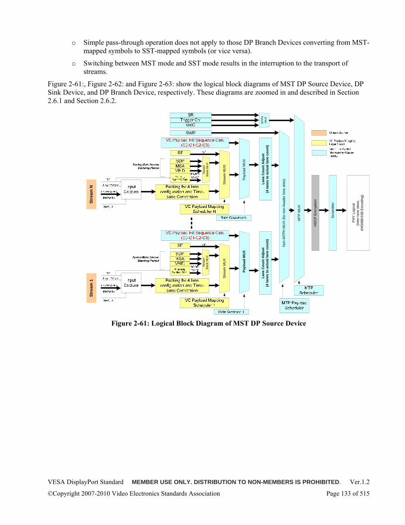
VESA DisplayPort Standard MEMBER USE ONLY. DISTRIBUTION TO NON-MEMBERS IS PROHIBITED. Ver.1.2
©Copyright 2007-2010 Video Electronics Standards Association Page 133 of 515
o Simple pass-through operation does not apply to those DP Branch Devices converting from MST-mapped symbols to SST-mapped symbols (or vice versa).
o Switching between MST mode and SST mode results in the interruption to the transport of streams.
Figure 2-61:, Figure 2-62: and Figure 2-63: show the logical block diagrams of MST DP Source Device, DP Sink Device, and DP Branch Device, respectively. These diagrams are zoomed in and described in Section 2.6.1 and Section 2.6.2.
Stre
am N
Stre
am 1
Stre
am M
UX
Pay
load
MU
X
Non
-MTP
H M
UX
(for
non
-hea
der t
ime
slot
s)
Stre
am M
UX
Payl
oad
MU
X
Stre
amBl
ank
MU
X
MTP
H
MU
X
PH
Y Lo
gica
l(In
ter-
lane
ske
w,
AN
SI8
B/1
0B E
ncod
ing)
HD
CP
Enc
rypt
ion
Scr
ambl
er
MTP
MU
X
Lane
Cou
nt A
djus
t (4
lane
s to
act
ual l
ane
coun
t)La
ne C
ount
Adj
ust
(4 la
nes
to a
ctua
l lan
e co
unt)
Stre
amB
lank
MU
X
Figure 2-61: Logical Block Diagram of MST DP Source Device
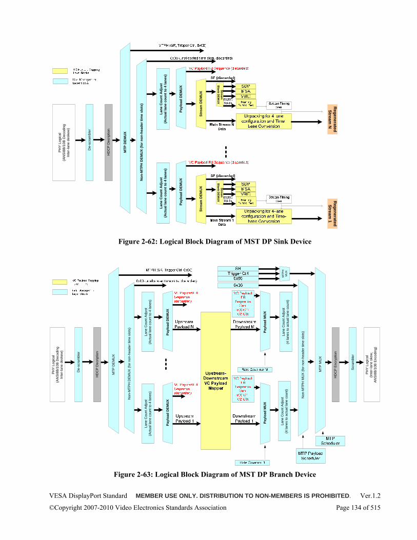
VESA DisplayPort Standard MEMBER USE ONLY. DISTRIBUTION TO NON-MEMBERS IS PROHIBITED. Ver.1.2
©Copyright 2007-2010 Video Electronics Standards Association Page 134 of 515
Regenerated Stream
NR
egenerated Stream
1
Stre
am D
EMU
X
Payl
oad
DEM
UX
Non
-MTP
H D
EMU
X (fo
r non
-hea
der t
ime
slot
s)
Payl
oad
DEM
UX
StreamB
lank DEM
UX
PH
Y L
ogic
al(A
NS
I8B/
10B
Dec
odin
gIn
ter-l
ane
desk
ew)
De-
scra
mbl
er
HD
CP
Dec
riptio
n
MTP
DEM
UX
Lane
Cou
nt A
djus
t (A
ctua
l lan
e co
unt t
o 4
lane
s)La
ne C
ount
Adj
ust
(Act
ual l
ane
coun
t to
4 la
nes)
StreamB
lank DEM
UX
Stre
am D
EMU
X
Figure 2-62: Logical Block Diagram of MST DP Sink Device
Payl
oad
DEM
UX
Non
-MTP
H D
EM
UX
(for
non
-hea
der t
ime
slot
s)
Payl
oad
DEM
UX
PH
Y L
ogic
al(A
NS
I8B
/10B
Dec
odin
gIn
ter-
lane
des
kew
)
De-
scra
mbl
er
HD
CP
Dec
riptio
n
Payl
oad
MU
X
Non
-MTP
H M
UX
(for
non
-hea
der t
ime
slot
s)
Payl
oad
MU
X
MTP
H
MU
X
PH
Y L
ogic
al(In
ter-
lane
ske
w,
AN
SI8
B/1
0B E
ncod
ing)
HD
CP
Enc
rypt
ion
Scr
ambl
er
MTP
MU
X
Lane
Cou
nt A
djus
t (4
lane
s to
act
ual l
ane
coun
t)
Lane
Cou
nt A
djus
t (A
ctua
l lan
e co
unt t
o 4
lane
s)
MTP
DE
MU
X
Lane
Cou
nt A
djus
t (A
ctua
l lan
e co
unt t
o 4
lane
s)
Lane
Cou
nt A
djus
t (4
lane
s to
act
ual l
ane
coun
t)
Figure 2-63: Logical Block Diagram of MST DP Branch Device
VESA DisplayPort Standard MEMBER USE ONLY. DISTRIBUTION TO NON-MEMBERS IS PROHIBITED. Ver.1.2
©Copyright 2007-2010 Video Electronics Standards Association Page 135 of 515
Figure 2-64: and Figure 2-65: show the logic block diagrams of SST DP Source device and DP Sink device for reference purpose. These diagrams, when compared to Figure 2-61: and Figure 2-62: illustrate the similarity of VC Payload Mapping Layer blocks between SST in 4-lane configuration and MST.
Mai
n St
ream
Stre
am M
UX
Stre
amB
lank
MU
X
PHY
Logi
cal
(Inte
r-la
ne s
kew
,A
NSI
8B/1
0B E
ncod
ing)
HD
CP
Encr
yptio
n
Scra
mbl
er
IDLE
BS
MU
X
Stre
am-ID
LE M
UX
SR In
sert
ion
(rep
laci
ng e
very
51
2th B
S)
Figure 2-64: Logical Block Diagram of SST DP Source Device
Unpacking (Lane Count Dependent) and Time-base Conversion
SDP
VBIDMSA
Main StreamData
Stream Timing Gen.
Link Management Layer blocks
Stream MappingLayer blocks
Stream Source
Figure 2-65: Logical Block Diagram of SST DP Sink Device
2.6.1 Link Timing Generation Based on Multi-Stream Transport Packet A uPacket TX enables an MST mode by setting MSTM_EN bit to 1 via Native AUX WR after having verified that its downstream uPacket RX has the MSTM_CAP bit set to 1.
In SST mode, Main Link timing is governed by the timing of the main stream the link it is transporting in that the BS/SR symbol insertion interval is dictated by the horizontal period of the main video stream. The TU (transfer unit), the vessel of micro packets in SST mode, is transported only during main video stream active
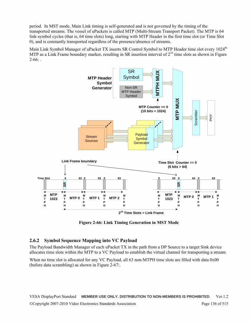
VESA DisplayPort Standard MEMBER USE ONLY. DISTRIBUTION TO NON-MEMBERS IS PROHIBITED. Ver.1.2
©Copyright 2007-2010 Video Electronics Standards Association Page 136 of 515
period. In MST mode, Main Link timing is self-generated and is not governed by the timing of the transported streams. The vessel of uPackets is called MTP (Multi-Stream Transport Packet). The MTP is 64 link-symbol cycles (that is, 64 time slots) long, starting with MTP Header in the first time slot (or Time Slot 0), and is constantly transported regardless of the presence/absence of streams.
Main Link Symbol Manager of uPacket TX inserts SR Control Symbol to MTP Header time slot every 1024th MTP as a Link Frame boundary marker, resulting in SR insertion interval of 216 time slots as shown in Figure 2-66: .
MTP
MU
X
Stream Sources
Scr
ambl
er
PHY
Payload Symbol
Generator
Time Slot Counter == 0(6 bits = 64)
MTP
H M
UXSR
Symbol
Non-SR MTP Header
Symbol
MTP Header Symbol
Generator
MTP Counter == 0(10 bits = 1024)
`
MTP 0 MTP 1 MTP 2MTP 1023 MTP 0 MTP 1MTP
1023
SR SRTime Slot
216 Time Slots = Link Frame
630 630 630 630 630 630
MTPH
MTPH
MTPH
MTPH
MTPH
MTPH
MTPH
MTPH
MTPH
Link Frame boundary
Figure 2-66: Link Timing Generation in MST Mode
2.6.2 Symbol Sequence Mapping into VC Payload The Payload Bandwidth Manager of each uPacket TX in the path from a DP Source to a target Sink device allocates time slots within the MTP to a VC Payload to establish the virtual channel for transporting a stream.
When no time slot is allocated for any VC Payload, all 63 non-MTPH time slots are filled with data 0x00 (before data scrambling) as shown in Figure 2-67:.
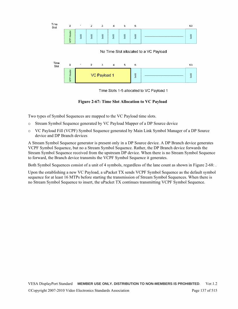
VESA DisplayPort Standard MEMBER USE ONLY. DISTRIBUTION TO NON-MEMBERS IS PROHIBITED. Ver.1.2
©Copyright 2007-2010 Video Electronics Standards Association Page 137 of 515
MTP
Hea
der
0x00
0x00
0x00
0x00
0x00
0x00
0x00
MTP
Hea
der
0x00
0x00
0x00
0x00
0x00
0x00
0x00
Figure 2-67: Time Slot Allocation to VC Payload
Two types of Symbol Sequences are mapped to the VC Payload time slots.
o Stream Symbol Sequence generated by VC Payload Mapper of a DP Source device
o VC Payload Fill (VCPF) Symbol Sequence generated by Main Link Symbol Manager of a DP Source device and DP Branch devices
A Stream Symbol Sequence generator is present only in a DP Source device. A DP Branch device generates VCPF Symbol Sequence, but no a Stream Symbol Sequence. Rather, the DP Branch device forwards the Stream Symbol Sequence received from the upstream DP device. When there is no Stream Symbol Sequence to forward, the Branch device transmits the VCPF Symbol Sequence it generates.
Both Symbol Sequences consist of a unit of 4 symbols, regardless of the lane count as shown in Figure 2-68: .
Upon the establishing a new VC Payload, a uPacket TX sends VCPF Symbol Sequence as the default symbol sequence for at least 16 MTPs before starting the transmission of Stream Symbol Sequences. When there is no Stream Symbol Sequence to insert, the uPacket TX continues transmitting VCPF Symbol Sequence.
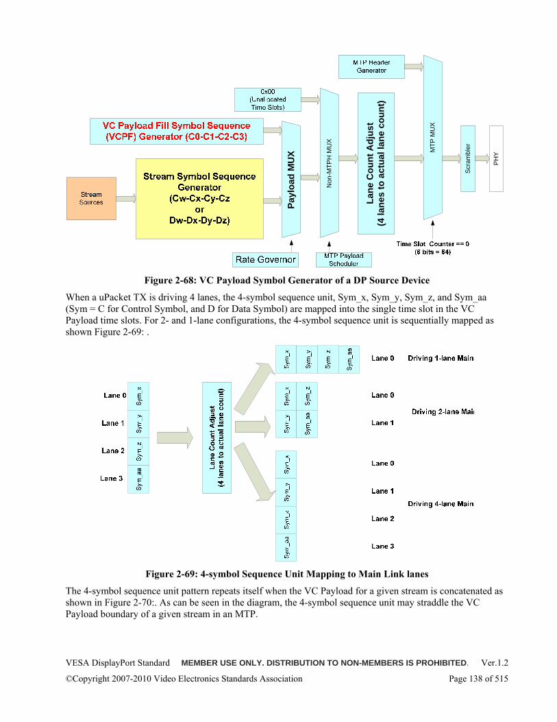
VESA DisplayPort Standard MEMBER USE ONLY. DISTRIBUTION TO NON-MEMBERS IS PROHIBITED. Ver.1.2
©Copyright 2007-2010 Video Electronics Standards Association Page 138 of 515
MTP
MU
X
Scra
mbl
er
PH
Y
Payl
oad
MU
X
Lane
Cou
nt A
djus
t (4
lane
s to
act
ual l
ane
coun
t)
Non
-MTP
H M
UX
Figure 2-68: VC Payload Symbol Generator of a DP Source Device
When a uPacket TX is driving 4 lanes, the 4-symbol sequence unit, Sym_x, Sym_y, Sym_z, and Sym_aa (Sym = C for Control Symbol, and D for Data Symbol) are mapped into the single time slot in the VC Payload time slots. For 2- and 1-lane configurations, the 4-symbol sequence unit is sequentially mapped as shown Figure 2-69: .
Figure 2-69: 4-symbol Sequence Unit Mapping to Main Link lanes
The 4-symbol sequence unit pattern repeats itself when the VC Payload for a given stream is concatenated as shown in Figure 2-70:. As can be seen in the diagram, the 4-symbol sequence unit may straddle the VC Payload boundary of a given stream in an MTP.
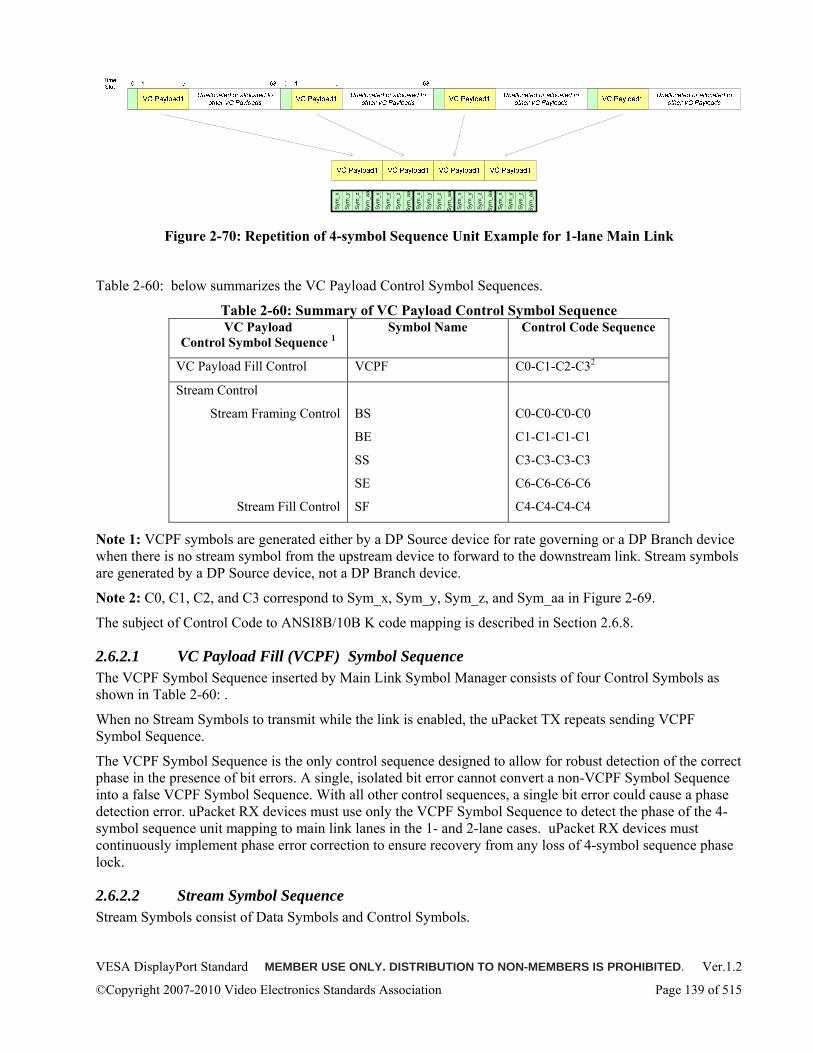
VESA DisplayPort Standard MEMBER USE ONLY. DISTRIBUTION TO NON-MEMBERS IS PROHIBITED. Ver.1.2
©Copyright 2007-2010 Video Electronics Standards Association Page 139 of 515
Sym
_x
Sym
_y
Sym
_z
Sym
_aa
Sym
_x
Sym
_y
Sym
_z
Sym
_aa
Sym
_x
Sym
_y
Sym
_z
Sym
_aa
Sym
_x
Sym
_y
Sym
_z
Sym
_aa
Sym
_x
Sym
_y
Sym
_z
Sym
_aa
Figure 2-70: Repetition of 4-symbol Sequence Unit Example for 1-lane Main Link
Table 2-60: below summarizes the VC Payload Control Symbol Sequences.
Table 2-60: Summary of VC Payload Control Symbol Sequence VC Payload
Control Symbol Sequence 1 Symbol Name Control Code Sequence
VC Payload Fill Control VCPF C0-C1-C2-C32
Stream Control
Stream Framing Control
Stream Fill Control
BS
BE
SS
SE
SF
C0-C0-C0-C0
C1-C1-C1-C1
C3-C3-C3-C3
C6-C6-C6-C6
C4-C4-C4-C4
Note 1: VCPF symbols are generated either by a DP Source device for rate governing or a DP Branch device when there is no stream symbol from the upstream device to forward to the downstream link. Stream symbols are generated by a DP Source device, not a DP Branch device.
Note 2: C0, C1, C2, and C3 correspond to Sym_x, Sym_y, Sym_z, and Sym_aa in Figure 2-69.
The subject of Control Code to ANSI8B/10B K code mapping is described in Section 2.6.8.
2.6.2.1 VC Payload Fill (VCPF) Symbol Sequence The VCPF Symbol Sequence inserted by Main Link Symbol Manager consists of four Control Symbols as shown in Table 2-60: .
When no Stream Symbols to transmit while the link is enabled, the uPacket TX repeats sending VCPF Symbol Sequence.
The VCPF Symbol Sequence is the only control sequence designed to allow for robust detection of the correct phase in the presence of bit errors. A single, isolated bit error cannot convert a non-VCPF Symbol Sequence into a false VCPF Symbol Sequence. With all other control sequences, a single bit error could cause a phase detection error. uPacket RX devices must use only the VCPF Symbol Sequence to detect the phase of the 4-symbol sequence unit mapping to main link lanes in the 1- and 2-lane cases. uPacket RX devices must continuously implement phase error correction to ensure recovery from any loss of 4-symbol sequence phase lock.
2.6.2.2 Stream Symbol Sequence Stream Symbols consist of Data Symbols and Control Symbols.
VESA DisplayPort Standard MEMBER USE ONLY. DISTRIBUTION TO NON-MEMBERS IS PROHIBITED. Ver.1.2
©Copyright 2007-2010 Video Electronics Standards Association Page 140 of 515
Control Symbols
o Stream Framing Control Symbols, namely, BS, BE, SS, and SE
o Stream Fill Control Symbols
o SF symbols are inserted when Rate Governor in a DP Source device selects Stream Symbol Sequence Generator side of Payload MUX (Figure 2-68: ), but VC Payload Mapper has no meaningful Stream Symbol Sequence to insert.
o During the blanking period of the main video stream, SF symbols are inserted by a DP Source device by default as there are no meaningful Stream Symbol Sequences to insert. Those SF symbols during the blanking period are replaced with Stream Framing Control Symbols, VB-ID Packet (namely, VB-ID, Mvid7:0, Maud7:0 immediately following BS Control Symbol Sequence), MSA Packet, and Secondary-Data Packets.
Control Code Sequence of the Stream Control Symbols is listed in Table 2-60: .
In SST mode, every 512th BS is replaced with SR for scrambler reset. In other words, BS is used not only as Stream Framing Control Symbol (blanking start, corresponding to Display Enable falling edge of the main video stream) but also as Link Timing Control Symbol, that is, SR as the Link Frame boundary and BS as the Link Line boundary. In order to enhance the error immunity of BS and SR Control Symbols, the SST has the Enhanced Framing Symbol Sequence option for BS and SR with which each of these two consists of 4 Control Symbols per lane.
In MST mode, the Link Frame boundary (SR, inserted once in 216 time slots) is completely decoupled from the timing of the stream the link is transporting. The BS symbol sequence is used as Stream Framing Control Symbol only and is never replaced with SR. The BS symbol sequence consists of 4-symbols regardless of the lane count..
Note: There is no Control Symbol marking the Link Line boundary in the MST mode. It should be noted, however, that a notion of a Link Line may be established for any upper layer protocol that requires Link Line boundary by setting the Link Line boundaries relative to the Link Frame boundary which is fixed to 216 time slots. For example, there will be 32 Link Lines per Link Frame if the Link Line interval is set to 32 MTP’s.
Data Symbols
o Main Stream Data Symbols
o VB-ID Packet (VB-ID/Mvid7:0/Maud7:0)
o MSA Packet Data Symbols
o Secondary-Data Packet (SDP) Data Symbols including Parity Byte Symbols
Stream Data Symbol mapping of MST mode is identical to that of SST mode in 4-lane Main Link configuration.
The AV stream is mapped into VC Payload time slots of the stream as shown in Figure 2-71: in MST mode regardless of the Main Link lane count the uPacket TX is driving. In case the lane count is 1- or 2- lanes, the Lane Count Adjust block (Figure 2-68: ) sequentially maps to the lane count as shown in Figure 2-69: .
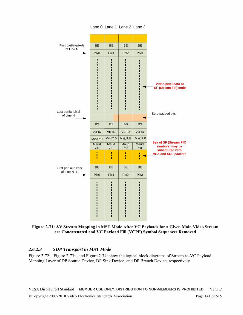
VESA DisplayPort Standard MEMBER USE ONLY. DISTRIBUTION TO NON-MEMBERS IS PROHIBITED. Ver.1.2
©Copyright 2007-2010 Video Electronics Standards Association Page 141 of 515
First partial-pixelsof Line N
Last partial-pixel of Line N Zero-padded bits
Pix0 Pix1 Pix2 Pix3
Pix0 Pix1 Pix2 Pix3
Sea of SF (Stream Fill) symbols; may be substituted with
MSA and SDP packets
First partial-pixelsof Line N+1
VB-IDVB-IDVB-ID VB-ID
Mvid7:0
Lane 0 Lane 1 Lane 2 Lane 3
Mvid7:0 Mvid7:0 Mvid7:0
Maud7:0
BS BS BS BS
BE BE BE BE
BE BE BE BE
Maud7:0
Maud7:0
Maud7:0
Video pixel data or SF (Stream Fill) code
Figure 2-71: AV Stream Mapping in MST Mode After VC Payloads for a Given Main Video Stream
are Concatenated and VC Payload Fill (VCPF) Symbol Sequences Removed
2.6.2.3 SDP Transport in MST Mode Figure 2-72: , Figure 2-73: , and Figure 2-74: show the logical block diagrams of Stream-to-VC Payload Mapping Layer of DP Source Device, DP Sink Device, and DP Branch Device, respectively.
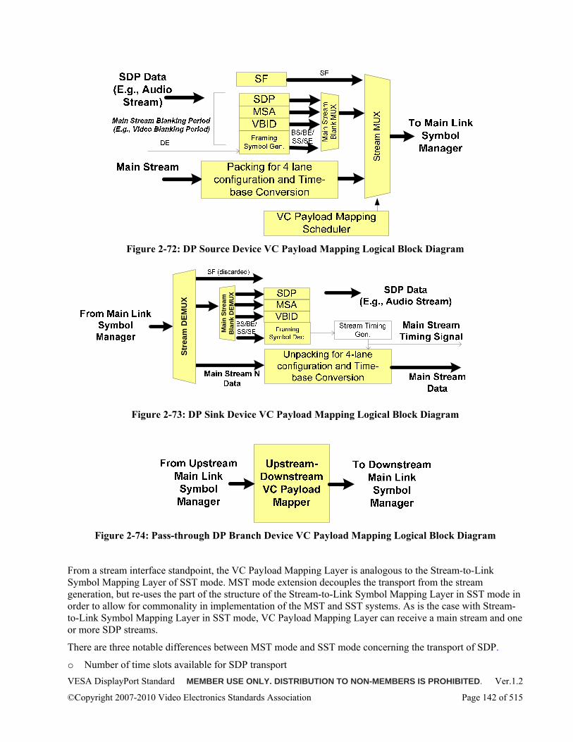
VESA DisplayPort Standard MEMBER USE ONLY. DISTRIBUTION TO NON-MEMBERS IS PROHIBITED. Ver.1.2
©Copyright 2007-2010 Video Electronics Standards Association Page 142 of 515
Figure 2-72: DP Source Device VC Payload Mapping Logical Block Diagram
Stre
am D
EMU
X
Mai
n St
ream
Bla
nk D
EMU
X
Figure 2-73: DP Sink Device VC Payload Mapping Logical Block Diagram
Figure 2-74: Pass-through DP Branch Device VC Payload Mapping Logical Block Diagram
From a stream interface standpoint, the VC Payload Mapping Layer is analogous to the Stream-to-Link Symbol Mapping Layer of SST mode. MST mode extension decouples the transport from the stream generation, but re-uses the part of the structure of the Stream-to-Link Symbol Mapping Layer in SST mode in order to allow for commonality in implementation of the MST and SST systems. As is the case with Stream-to-Link Symbol Mapping Layer in SST mode, VC Payload Mapping Layer can receive a main stream and one or more SDP streams.
There are three notable differences between MST mode and SST mode concerning the transport of SDP.
o Number of time slots available for SDP transport
VESA DisplayPort Standard MEMBER USE ONLY. DISTRIBUTION TO NON-MEMBERS IS PROHIBITED. Ver.1.2
©Copyright 2007-2010 Video Electronics Standards Association Page 143 of 515
o Splitting of SDP
o Transport of SDP-only without a main stream
2.6.2.3.1 Number of Data Symbols Available for SDP Transport (Informative) In MST mode, Main Link Symbol Mapper of uPacket TX reads symbols from VC Payload Mapper in a DP Source device on every link symbol clock edge when the Rate Governor selects the Stream Symbol Sequence Generator side of Payload MUX during the VC Payload time slots for the stream. When there is no main stream data and VB-ID Packet/MSA Packet to transmit, SDP may be transported.
This sub-section is informative as the number of SDP payloads to be transported is dependent on how the Source device packs the SDP. In this section, the example is shown where the SDP payload size is fixed to 32 bytes. Concatenating the payloads within a single SDP reduces the time slot usage overhead for SDP header and SE symbol insertion, and thus increases the data symbols available for SDP payload transport.
The number of MTPs per main video stream horizontal blanking period (MtpCntPerHBlank) is:
TimeSlottHBlanktBlankMtpCntPerH_*64
_=
where t_HBlank is the main video stream horizontal blanking period and t_TimeSlot is the link time slot period (that is, the Link Symbol Clock period).
The number of Stream Symbols per t_HBlank (StrmSymblCntPerHBlank) is:
LaneCntSIZEVCPThrottledlankMtpCntPerBkntPerHBlanStrmSmyblC *__*=
where LaneCnt is the lane count of the main link.
During t_Blank, BS, VB-ID Packet, and BE symbol sequence must be sent, resulting in 20 of StrmSymblCntPerBlank used for these symbols. Therefore, the number of Stream Symbols available for SDP is as follows:
20−= kntPerHBlanStrmSymblCrHBlankntForSdpPeStrmSymblC
SDP data has an overhead of SS, SE, Header, and Parity. SdpDataEfficiency is:
dSdpOverheaeSdpDataSizeSdpDataSiziciencySdpDataEff
+=
When the SDP data size is 32 bytes, for example, the total overhead is 24 bytes. Therefore, SdpDataEfficiency becomes:
74
243232
=+
=iciencySdpDataEff
The number of symbols available for SDP Data per t_HBlank (SdpDataSymbolCnt) is:
iciencySdpDataEffrHBlankntForSdpPeStrmSymblClCntSdpDataSmb *=
The resulting SdpDataRate is:
HPeriodtlCntSdpDataSmbeSdpDataRat _/=
The SdpDataRate must be equal to or larger than the peak data rate of the stream packed into the SDPs.
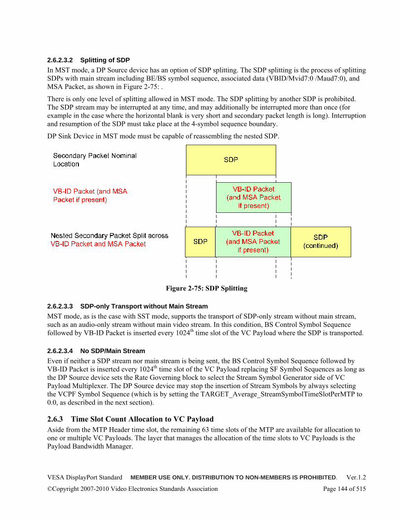
VESA DisplayPort Standard MEMBER USE ONLY. DISTRIBUTION TO NON-MEMBERS IS PROHIBITED. Ver.1.2
©Copyright 2007-2010 Video Electronics Standards Association Page 144 of 515
2.6.2.3.2 Splitting of SDP In MST mode, a DP Source device has an option of SDP splitting. The SDP splitting is the process of splitting SDPs with main stream including BE/BS symbol sequence, associated data (VBID/Mvid7:0 /Maud7:0), and MSA Packet, as shown in Figure 2-75: .
There is only one level of splitting allowed in MST mode. The SDP splitting by another SDP is prohibited. The SDP stream may be interrupted at any time, and may additionally be interrupted more than once (for example in the case where the horizontal blank is very short and secondary packet length is long). Interruption and resumption of the SDP must take place at the 4-symbol sequence boundary.
DP Sink Device in MST mode must be capable of reassembling the nested SDP.
Figure 2-75: SDP Splitting
2.6.2.3.3 SDP-only Transport without Main Stream MST mode, as is the case with SST mode, supports the transport of SDP-only stream without main stream, such as an audio-only stream without main video stream. In this condition, BS Control Symbol Sequence followed by VB-ID Packet is inserted every 1024th time slot of the VC Payload where the SDP is transported.
2.6.2.3.4 No SDP/Main Stream Even if neither a SDP stream nor main stream is being sent, the BS Control Symbol Sequence followed by VB-ID Packet is inserted every 1024th time slot of the VC Payload replacing SF Symbol Sequences as long as the DP Source device sets the Rate Governing block to select the Stream Symbol Generator side of VC Payload Multiplexer. The DP Source device may stop the insertion of Stream Symbols by always selecting the VCPF Symbol Sequence (which is by setting the TARGET_Average_StreamSymbolTimeSlotPerMTP to 0.0, as described in the next section).
2.6.3 Time Slot Count Allocation to VC Payload Aside from the MTP Header time slot, the remaining 63 time slots of the MTP are available for allocation to one or multiple VC Payloads. The layer that manages the allocation of the time slots to VC Payloads is the Payload Bandwidth Manager.
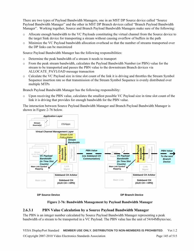
VESA DisplayPort Standard MEMBER USE ONLY. DISTRIBUTION TO NON-MEMBERS IS PROHIBITED. Ver.1.2
©Copyright 2007-2010 Video Electronics Standards Association Page 145 of 515
There are two types of Payload Bandwidth Managers, one in an MST DP Source device called “Source Payload Bandwidth Manager” and the other in MST DP Branch devices called “Branch Payload Bandwidth Manager”. Working together, Source and Branch Payload Bandwidth Managers make sure of the following:
o Allocate enough bandwidth to the VC Payloads constituting the virtual channel from the Source device to the target Sink device for transporting a stream without causing overflow of buffers in the path
o Minimize the VC Payload bandwidth allocation overhead so that the number of streams transported over the DP links can be maximized
Source Payload Bandwidth Manager has the following responsibilities:
o Determine the peak bandwidth of a stream it needs to transport o From the peak stream bandwidth, calculates the Payload Bandwidth Number (or PBN) value for the
stream to be transported and passes the PBN value to the downstream Branch devices via ALLOCATE_PAYLOAD message transaction
o Calculate the VC Payload size in time slot count of the link it is driving and throttles the Stream Symbol Sequence insertion rate so that transmission of the Stream Symbol Sequence is evenly distributed over multiple MTPs
Branch Payload Bandwidth Manager has the following responsibility:
o Upon receiving the PBN value, calculates the smallest possible VC Payload size in time slot count of the link it is driving that provides for enough bandwidth for the PBN value.
The interaction between Source Payload Bandwidth Manager and Branch Payload Bandwidth Manager is shown in Figure 2-76 below.
Virtual Channel Management Layer
Application Layer
OS/Apps
Stream /LinkPolicy Maker
Stream Source(s)
Link Mgmt
Main Link Symbol Mapping
Main Link
Stream-to-VC Payload
Mapping(s)
...
...
Sideband CH(AUX CH + HPD)
Sideband CH Arbitor
Main Link Symbol Mapping
Main Link
Stream-to-VC Payload
Mapping(s)
...
Sideband CH(AUX CH + HPD)
Sideband CH Arbitor
Stream Bandwidth
VC Payload Bandwidth(in Time Slot Counts)
PBN Value
(via Sideband CH Communiation)
VC Payload Bandwidth(in Time Slot Counts)
DP Source Device DP Branch Device
PBN Value
To the nextBranch DeviceSo
urce
Pay
load
B
andw
idth
M
anag
emen
t
Topo
logy
M
anag
emen
t
Bra
nch
Payl
oad
Ban
dwid
th
Man
agem
ent
Link Mgmt
Topo
logy
M
anag
emen
t
Figure 2-76: Bandwidth Management by Payload Bandwidth Manager
2.6.3.1 PBN Value Calculation by a Source Payload Bandwidth Manager The PBN is an integer number calculated by Source Payload Bandwidth Manager representing a peak bandwidth of a stream to be transported in a VC Payload. The PBN value has the unit of 54/64Mbytes/sec.
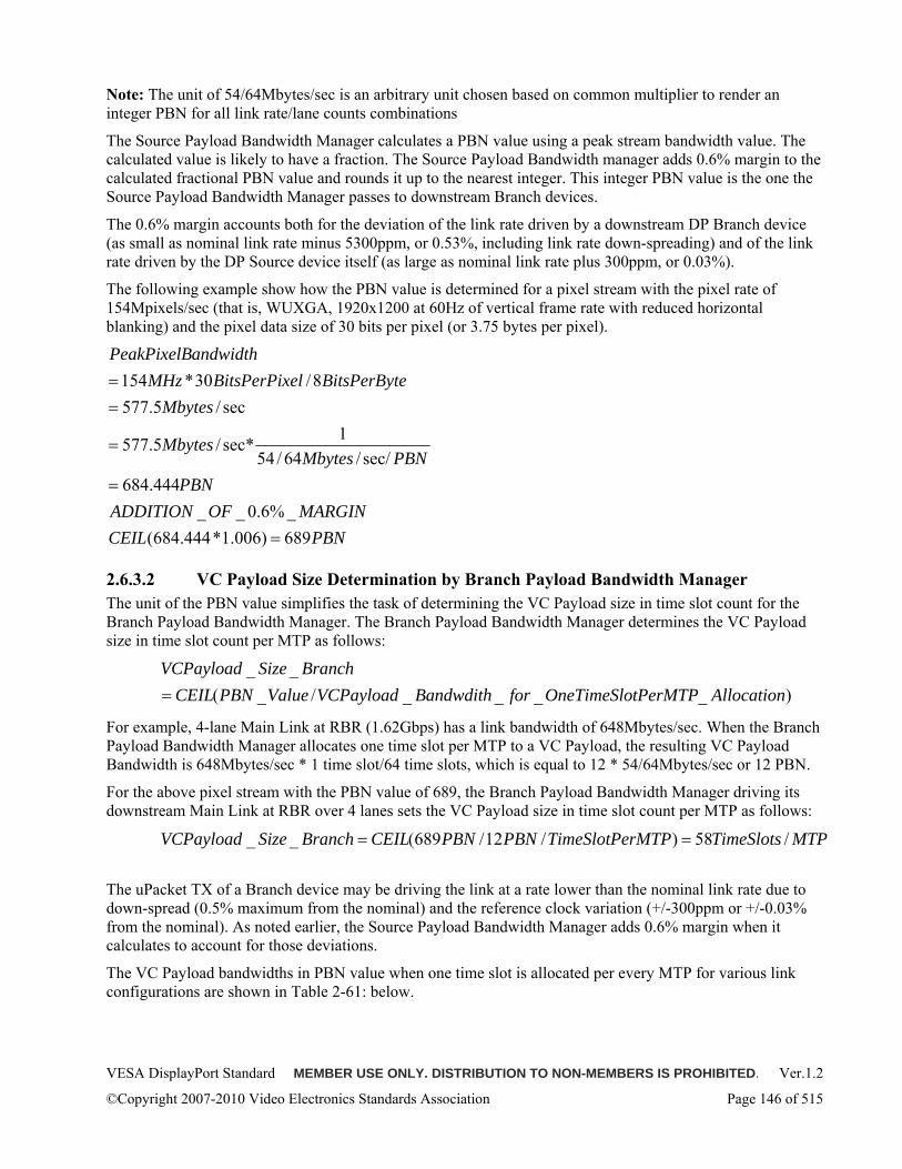
VESA DisplayPort Standard MEMBER USE ONLY. DISTRIBUTION TO NON-MEMBERS IS PROHIBITED. Ver.1.2
©Copyright 2007-2010 Video Electronics Standards Association Page 146 of 515
Note: The unit of 54/64Mbytes/sec is an arbitrary unit chosen based on common multiplier to render an integer PBN for all link rate/lane counts combinations
The Source Payload Bandwidth Manager calculates a PBN value using a peak stream bandwidth value. The calculated value is likely to have a fraction. The Source Payload Bandwidth manager adds 0.6% margin to the calculated fractional PBN value and rounds it up to the nearest integer. This integer PBN value is the one the Source Payload Bandwidth Manager passes to downstream Branch devices.
The 0.6% margin accounts both for the deviation of the link rate driven by a downstream DP Branch device (as small as nominal link rate minus 5300ppm, or 0.53%, including link rate down-spreading) and of the link rate driven by the DP Source device itself (as large as nominal link rate plus 300ppm, or 0.03%).
The following example show how the PBN value is determined for a pixel stream with the pixel rate of 154Mpixels/sec (that is, WUXGA, 1920x1200 at 60Hz of vertical frame rate with reduced horizontal blanking) and the pixel data size of 30 bits per pixel (or 3.75 bytes per pixel).
PBNCEILMARGINOFADDITION
PBNPBNMbytes
Mbytes
MbyteseBitsPerBytelBitsPerPixMHz
andwidthPeakPixelB
689)006.1*444.684(_%6.0__
444.684sec//64/54
1sec*/5.577
sec/5.5778/30*154
=
=
=
==
2.6.3.2 VC Payload Size Determination by Branch Payload Bandwidth Manager The unit of the PBN value simplifies the task of determining the VC Payload size in time slot count for the Branch Payload Bandwidth Manager. The Branch Payload Bandwidth Manager determines the VC Payload size in time slot count per MTP as follows:
)____/_(__
AllocationtPerMTPOneTimeSloforBandwdithVCPayloadValuePBNCEILBranchSizeVCPayload
=
For example, 4-lane Main Link at RBR (1.62Gbps) has a link bandwidth of 648Mbytes/sec. When the Branch Payload Bandwidth Manager allocates one time slot per MTP to a VC Payload, the resulting VC Payload Bandwidth is 648Mbytes/sec * 1 time slot/64 time slots, which is equal to 12 * 54/64Mbytes/sec or 12 PBN.
For the above pixel stream with the PBN value of 689, the Branch Payload Bandwidth Manager driving its downstream Main Link at RBR over 4 lanes sets the VC Payload size in time slot count per MTP as follows:
MTPTimeSlotsrMTPTimeSlotPePBNPBNCEILBranchSizeVCPayload /58)/12/689(__ ==
The uPacket TX of a Branch device may be driving the link at a rate lower than the nominal link rate due to down-spread (0.5% maximum from the nominal) and the reference clock variation (+/-300ppm or +/-0.03% from the nominal). As noted earlier, the Source Payload Bandwidth Manager adds 0.6% margin when it calculates to account for those deviations.
The VC Payload bandwidths in PBN value when one time slot is allocated per every MTP for various link configurations are shown in Table 2-61: below.
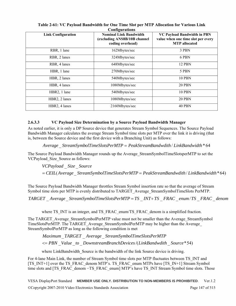
VESA DisplayPort Standard MEMBER USE ONLY. DISTRIBUTION TO NON-MEMBERS IS PROHIBITED. Ver.1.2
©Copyright 2007-2010 Video Electronics Standards Association Page 147 of 515
Table 2-61: VC Payload Bandwidth for One Time Slot per MTP Allocation for Various Link Configurations
Link Configuration Nominal Link Bandwidth (excluding ANS8B/10B channel
coding overhead)
VC Payload Bandwidth in PBN value when one time slot per every
MTP allocated
RBR, 1 lane 162Mbytes/sec 3 PBN
RBR, 2 lanes 324Mbytes/sec 6 PBN
RBR, 4 lanes 648Mbytes/sec 12 PBN
HBR, 1 lane 270Mbytes/sec 5 PBN
HBR, 2 lanes 540Mbytes/sec 10 PBN
HBR, 4 lanes 1080Mbytes/sec 20 PBN
HBR2, 1 lane 540Mbytes/sec 10 PBN
HBR2, 2 lanes 1080Mbytes/sec 20 PBN
HBR2, 4 lanes 2160Mbytes/sec 40 PBN
2.6.3.3 VC Payload Size Determination by a Source Payload Bandwidth Manager As noted earlier, it is only a DP Source device that generates Stream Symbol Sequences. The Source Payload Bandwidth Manager calculates the average Stream Symbol time slots per MTP over the link it is driving (that is, between the Source device and the first device with a Branching Unit) as follows:
64*/_ dthLinkBandwiBandwdithPeakStreamsPerMTPolTimeSlotStreamSymbAverage =
The Source Payload Bandwidth Manager rounds up the Average_StreamSymbolTimeSlotsperMTP to set the VCPayload_Size_Source as follows:
)64*/_(__
dthLinkBandwiBandwdithPeakStreamsPerMTPolTimeSlotStreamSymbAverageCEILSourceSizeVCPayload
==
The Source Payload Bandwidth Manager throttles Stream Symbol insertion rate so that the average of Stream Symbol time slots per MTP is evenly distributed to TARGET_Average_StreamSymbolTimeSlots PerMTP.
denomFRACTSenumFRACTSINTTSsPerMTPolTimeSlotStreamSymbAverageTARGET __/_____ +=
where TS_INT is an integer, and TS_FRAC_enum/TS_FRAC_denom is a simplified fraction.
The TARGET_Average_StreamSymbolPerMTP value must not be smaller than the Average_StreamSymbol TimeSlotsPerMTP. The TARGET_Average_StreamSymbolPerMTP may be higher than the Average_ StreamSymbolPerMTP as long as the following condition is met
)54*_(/______
SourceithLinkBandwdcesBranchDeviDownstreamtoValuePBNsPerMTPolTimeSlotStreamSymbAverageTARGETMaximum
<=
where LinkBandwidth_Source is the bandwidth of the link Source device is driving.
For 4-lane Main Link, the number of Stream Symbol time slots per MTP fluctuates between TS_INT and [TS_INT+1] over the TS_FRAC_denom MTP’s. TS_FRAC_enum MTPs have [TS_IN+1] Stream Symbol time slots and [TS_FRAC_denom −TS_FRAC_enum] MTP’s have TS_INT Stream Symbol time slots. Those
VESA DisplayPort Standard MEMBER USE ONLY. DISTRIBUTION TO NON-MEMBERS IS PROHIBITED. Ver.1.2
©Copyright 2007-2010 Video Electronics Standards Association Page 148 of 515
TS_FRAC_enum MTPs with [TS_INT+1] Stream Symbol time slots must be evenly distributed over TS_FRAC_denom MTPs.
For 1-lane and 2-lane Main Link configurations, the fact that Symbol Sequences are 4 symbol multiples affects how the Stream Symbols insertion rate get throttled. Over the [TS_FRAC_denom * 4 /LaneCount] MTPs the Stream Symbols per MTP must be evenly distributed to TARGET_Average_StreamSymbol PerMTP value.
When the PeakStreamBandwidth is 577.5Mbytes/sec and when the bandwidth of the link Source device is driving is 1080Mbytes/sec (that is, 4-lane HBR),
222.3464sec*/1080sec//5.577_ == MbytesMbytessPerMTPolTimeSlotStreamSymbAverage
Therefore, the Source Payload Bandwidth Manager sets the VCPayload_Size_Source to 35 time slots. The maximum allowed TARGET_Average_StreamSymbolTimeSlotsPerMTP is:
MaximumTarget_Average_StreamSymbolTimeSlotsPerMTP
= 689*64*(54/64)/1080 = 34.45
So, the Source Payload Bandwidth Manager may set the TARGET_Average_StreamSymbolTimeSlotsPerMTP to 34.25, that is, TS_INT = 34, TS_FRAC_enum = 1, TS_FRAC_denom = 4.
1 out of 4 MTPs has 35 Stream Symbol time slots with 0 VCPF Symbol time slots within the VC Payload and 3 out of 4 MTPs has 34 Stream Symbol time slots with 1 VCPF Symbol time slot.
2.6.3.3.1 Maximum Allowed Rate Governing Deviation from Target Average for a Source Device A DP Source device must throttle the Stream Symbol insertion rate so that the accumulation of transmitted stream symbol count is in the following range at the beginning of any MTP:
ntdSymbolCouAccumulateTARGETntdSymbolCouAccumulateACTUALntdSymbolCouAccumulateTARGETntdSymbolCouAccumulateACTUAL
__8__
<=−>
The remainder of this subsection (Section 2.6.3.3.1) describes the rational behind the maximum allowed rate governing deviation above and should be regarded as informative.
For each MTP, the target number of transmitted Stream Symbols for a given VC Payload is M:
)__/___(* DENOMFRACTSENUMFRACTSINTTSLaneCountM +=
For each MTP, the actual number of transmitted Stream Symbols is N:
∑ −=
PayloadinVCTimeSlots
RGLaneCountN )(
where RG = 4 if the time slot is occupied by the first VCPF code (VCPF0, or C0), and RG = 0 otherwise. Note that VCPF Symbols occupy 4/LANECOUNT timeslots so the fact that N temporarily decreases for LANE_COUNT smaller than 4-inches represents the fact that a decision to introduce VCPF0 on a given time slot will cause subsequent timeslot(s) to be occupied by the remaining VCPF codes (C1, C2, and C3). (It should be noted that an insertion of VCPF Symbol in a VC Payload in one MTP may span to the VC Payload of the next MTP in case of 1- and 2-lane Main Link.)
Compute the accumulation of delta D between target and actual numbers of transmitted symbols:
)('
MNDsMTP
−= ∑
The D value is per MTP, not per time slot in a given MTP.
VESA DisplayPort Standard MEMBER USE ONLY. DISTRIBUTION TO NON-MEMBERS IS PROHIBITED. Ver.1.2
©Copyright 2007-2010 Video Electronics Standards Association Page 149 of 515
Insert VCPF0 (the first code of VCPF Symbol Sequence) if and only if D will otherwise exceed zero.
Summarizing,
))__/___(*)((('
DENOMFRACTSENUNFRACTSINTTSLaneCountRGLaneCountDPayloadinVC
TimeSlotssMTP+−−= ∑∑
where RG = 0 or 4.
The limit on the variability of D is determined by the following factors:
1. Since symbols are inserted in sets of four and the constraint D ≤ 0 must be met, the VCPF insertion algorithm must insert VCPF symbol if and only if the D value on the current timeslot would be less than four with a VCPF symbol inserted. The resulting variability is
. 2. Since VCPF symbols are inserted in sets of four, in the 1-lane case a decision to insert
VCPF0 will result in VCPF1 ~ VCPF3 in the next three allocated timeslots. The resulting variability is .In the 2-lane case, only the next allocated timeslot after the start of VCPF Symbol Sequence will contain VCPF symbol, and in the 4-lane case, each VCPF Symbol Sequence is transmitted completely within the single time slot.
Adding up Delta1 and Delta2, , determines the minimum possible variability range for D. For simplicity (since all symbols are managed in sets of four at the Stream to VC Payload Mapping Layer), the range of D (when measured at the start of an MTP) is constrained to:
− 8 < D <= 0
Thus, the contribution to the rate variability observed at the uPacket RX due to rate governing in the Source device is eight symbols.
2.6.3.3.2 Rate Governing Sample Pseudo-Code (Informative) The following pseudo-code is provided to show how rate governing could be implemented with a simple state machine. Note that this is example implementation for reference purposes only.
RG Parameters: D // range of D is -256 to 0 so 8 integer (no sign) bits are required; number of fractional bits is equal to number of bits of Y value X.Y // X.Y calculated by multiplying TARGET_Average_StreamSymbolTimeSlotPerMTP by Lane Count. X is an 8-bit value in the range 0 to 252, Y is implementation-dependent but should be at least 2 bits and ideally more
Other Parameters (not specifically for rate governing but referenced below): PHASE // 2-bit value to represent the four phases in the single-lane case, or two phases in two-lane case LANE_COUNT // 2-bit value; 1 = 1-lane, 2 = 2-lane, 0 = 4-lane
Initial condition and no time slot allocated to a VC Payload: Set D = 0 Set X.Y = 0 Set PHASE=0
At least sixteen symbols after ACT for new VC Payload time slot allocation, and any time for existing or reallocated VC Payload: Update X.Y to nonzero value (new X.Y automatically takes effect on next MTPH)
If MTPH Timeslot
VESA DisplayPort Standard MEMBER USE ONLY. DISTRIBUTION TO NON-MEMBERS IS PROHIBITED. Ver.1.2
©Copyright 2007-2010 Video Electronics Standards Association Page 150 of 515
D = D - X.Y else if VC Timeslot if PHASE = 0 // Only decide whether to start RG or VC data on phase zero since both are transmitted in sets of four if D <= -4 // Ensures that four Stream Symbols cannot cause D > 0 Read (from VC Payload Mapper) and start transmitting set of four Stream Symbols D <= D + 4 // Decrement D by amount of data that will be transmitted (some may be in subsequent timeslots) else start Rate Governing // Don’t update D since no data was sent else continue previously started 4-symbol sequence (VCPF Symbols or Stream Symbols) // Don’t update D since the change in D (if any) in the PHASE=0 case was already accounted for PHASE = PHASE + LANE_COUNT
2.6.4 VC Payload Allocation Synchronization Management Prior to starting a stream transfer from a stream Source to a stream Sink, a stream policy maker, based on the topology map information provided by Topology Manager, establishes the virtual channel connection between the stream Source and the stream Sink with the help of Payload Bandwidth Managers in the DP Source device and the DP Branch devices in the path. The virtual channel is mapped to a VC Payload on a DP link by Payload Bandwidth Manager.
The Payload Bandwidth Manager establishes and maintains VC Payloads it is receiving and transmitting/forwarding by managing VC Payload ID Table. The Payload Bandwidth Manager:
o Keeps its table synchronized with that of the uPacket RX of the downstream device it is driving through Native AUX transactions
o Also keeps the VC Payload time slot allocation over the Main Link synchronized with the table through ACT Trigger control sequence inserted in MTP Header time slots.
Each uPacket TX and uPacket RX has the VC Payload ID Table. The table within uPacket RX is mapped to the DPCD Address space as shown in the table below. It should be noted that reading of this VC Payload ID Table of uPacket RX by the Payload Bandwidth Manager of the immediate upstream uPacket TX is not required for normal operation. When to read this table (example, for debugging purposes) is an implementation choice for developers of DP Source and Branch devices
Though it is possible for an upstream device to update the VC Payload ID Table of a remote downstream device via REMOTE_DPCD message transaction, the remote update of a VC Payload ID Table is prohibited. Only the immediate upstream device is allowed to update the VC Payload ID Table of the downstream device as the only immediate upstream device is capable of initiating the ACT Trigger control sequence over the Main Link.
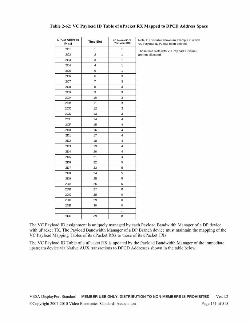
VESA DisplayPort Standard MEMBER USE ONLY. DISTRIBUTION TO NON-MEMBERS IS PROHIBITED. Ver.1.2
©Copyright 2007-2010 Video Electronics Standards Association Page 151 of 515
Table 2-62: VC Payload ID Table of uPacket RX Mapped to DPCD Address Space
DPCD Address(Hex)
2C3
2FF
2DE
...
2DD
2DC
2DB
2DA
2D9
2D8
2D7
2D6
2D5
2D4
2D3
2D2
2C1
2D1
2C2
2D0
2CF
2CE
2CD
2CC
2CB
2CA
2C9
2C8
2C7
2C6
2C5
2C4
Time Slot
1
2
3
4
63
30
...
29
28
27
26
25
24
23
22
21
20
19
18
17
16
15
14
13
12
11
10
9
8
7
6
5
VC Payload ID *1(7-bit value RO)
1
1
1
1
0
0
...
0
0
0
5
5
5
5
5
4
4
4
4
4
4
4
4
3
3
3
3
3
3
3
3
1
Note 1: This table shows an example in which VC Payload ID #2 has been deleted.
Those time slots with VC Payload ID value 0 are not allocated.
The VC Payload ID assignment is uniquely managed by each Payload Bandwidth Manager of a DP device with uPacket TX. The Payload Bandwidth Manager of a DP Branch device must maintain the mapping of the VC Payload Mapping Tables of its uPacket RXs to those of its uPacket TXs.
The VC Payload ID Table of a uPacket RX is updated by the Payload Bandwidth Manager of the immediate upstream device via Native AUX transactions to DPCD Addresses shown in the table below.
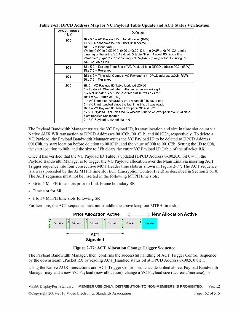
VESA DisplayPort Standard MEMBER USE ONLY. DISTRIBUTION TO NON-MEMBERS IS PROHIBITED. Ver.1.2
©Copyright 2007-2010 Video Electronics Standards Association Page 152 of 515
Table 2-63: DPCD Address Map for VC Payload Table Update and ACT Status Verification
The Payload Bandwidth Manager writes the VC Payload ID, its start location and size in time slot count via Native AUX WR transaction to DPCD Addresses 001C0h, 001C1h, and 001C2h, respectively. To delete a VC Payload, the Payload Bandwidth Manager writes the VC Payload ID to be deleted to DPCD Address 001C0h, its start location before deletion to 001C1h, and the value of 00h to 001C2h. Setting the ID to 00h, the start location to 00h, and the size to 3Fh clears the entire VC Payload ID Table of the uPacket RX.
Once it has verified that the VC Payload ID Table is updated (DPCD Address 0x002C0, bit 0 = 1), the Payload Bandwidth Manager is to trigger the VC Payload allocation over the Main Link via inserting ACT Trigger sequence into four consecutive MCT Header time slots as shown in Figure 2-77. The ACT sequence is always preceded by the 32 MTPH time slot ECF (Encryption Control Field) as described in Section 2.6.10. The ACT sequence must not be inserted in the following MTPH time slots:
36 to 5 MTPH time slots prior to Link Frame boundary SR
Time slot for SR
1 to 34 MTPH time slots following SR
Furthermore, the ACT sequence must not straddle the above keep-out MTPH time slots.
Figure 2-77: ACT Allocation Change Trigger Sequence
The Payload Bandwidth Manager, then, confirms the successful handling of ACT Trigger Control Sequence by the downstream uPacket RX by reading ACT_Handled status bit at DPCD Address 0x002C0 bit 1.
Using the Native AUX transactions and ACT Trigger Control sequence described above, Payload Bandwidth Manager may add a new VC Payload (new allocation), change a VC Payload size (decrease/increase), or
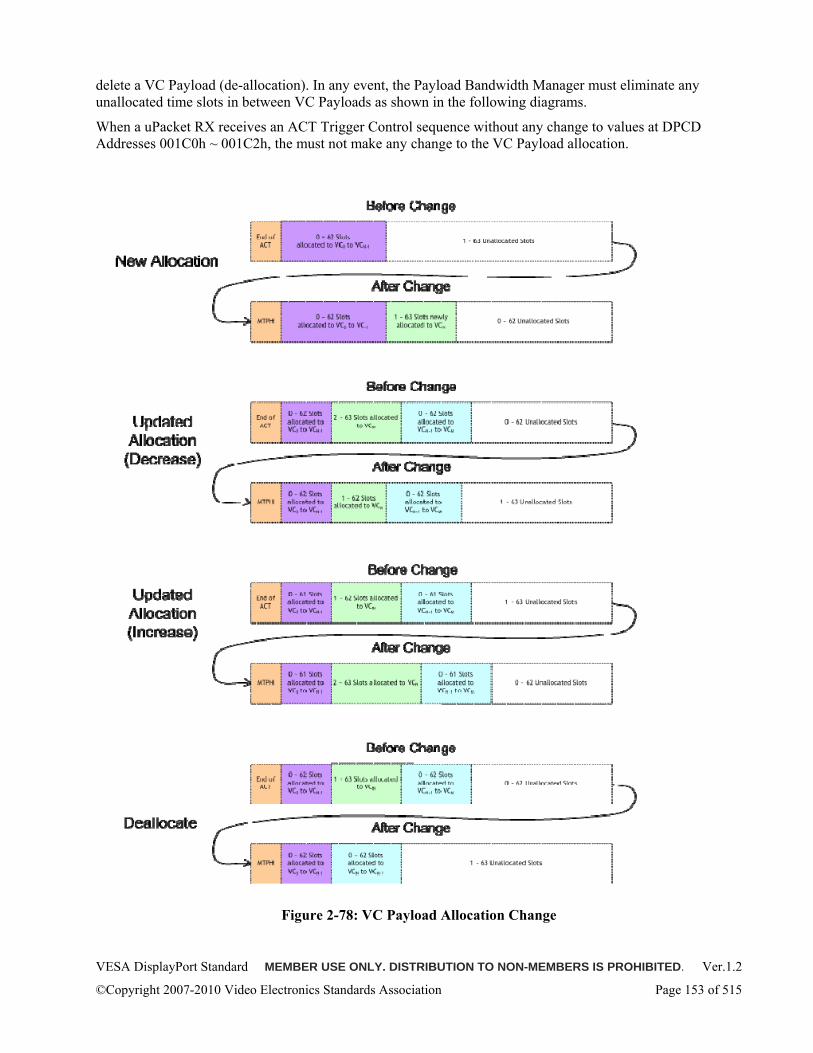
VESA DisplayPort Standard MEMBER USE ONLY. DISTRIBUTION TO NON-MEMBERS IS PROHIBITED. Ver.1.2
©Copyright 2007-2010 Video Electronics Standards Association Page 153 of 515
delete a VC Payload (de-allocation). In any event, the Payload Bandwidth Manager must eliminate any unallocated time slots in between VC Payloads as shown in the following diagrams.
When a uPacket RX receives an ACT Trigger Control sequence without any change to values at DPCD Addresses 001C0h ~ 001C2h, the must not make any change to the VC Payload allocation.
Figure 2-78: VC Payload Allocation Change
VESA DisplayPort Standard MEMBER USE ONLY. DISTRIBUTION TO NON-MEMBERS IS PROHIBITED. Ver.1.2
©Copyright 2007-2010 Video Electronics Standards Association Page 154 of 515
2.6.5 ALLOCATE_PAYLOAD Timing Sequence In order to synchronize the VC Payload time slot allocation change across the multiple links of the path, Payload Bandwidth Manager issues ALLOCATE_PAYLOAD Message Transaction. This section describes the timing sequence of interactions among Payload Bandwidth Manager, Main Link Symbol Manager, and VC Payload Mapper surrounding ALLOCATE_PAYLOAD Message Transaction
The ALLOCATE_PAYLOAD Message Transaction uses VC Payload ID and PBN value as the variables of this transaction. Optionally, the MST DP Source Device may execute ENUM_PATH_RESOURCES Message Transaction to check the available PBN value of the path before executing ALLOCATE_PAYLOAD Message Transaction.
An MST Source device targets both ENUM_PATH_RESOURCES and ALLOCATE_PAYLOAD at the last MST device with a branching unit driving a stream sink. In other words, the Payload Bandwidth Manager of a DP Source device sets the Relative Address (RAD) field of the header of the Message Transaction to point to the last MST device with a branching unit. The port number (either physical or logical) of the branching unit to which the Sink device is plugged to is included in the body of the Message Transaction.
When transporting an SDP stream (such as an audio stream), the Payload Bandwidth Manager of a DP Source device specifies the SDP stream sink number in the body of the ALLOCATE_PAYLOAD Message Transaction.
A timing sequence for adding a new payload is shown in Figure 2-79: . The Payload Bandwidth Manager of each uPacket TX in the path, upon receiving ALLOCATE_PAYLOAD message transaction, updates the VC Payload ID Table and VC Payload time slot allocation using the procedures described in Section 2.6.4. Once successful, it forwards the message transaction to its downstream DP device in the path.
When the Payload Bandwidth Manager of a DP Source device verifies that the ACT Trigger Control sequence has been successfully handled by the uPacket RX of the downstream device, it may set the Throttled_VCP_SIZE (that is, X.Y) value to the non-zero value to start the Stream Symbol Sequence insertion at least 16 MTPs after the new VC Payload is established.
The Payload Bandwidth manager of a DP Branch device, upon verifying the successful handling of the ACT Trigger, waits for 16 MTPs after the new VC Payload is established and starts forwarding Stream Symbol Sequence from the upstream DP device.
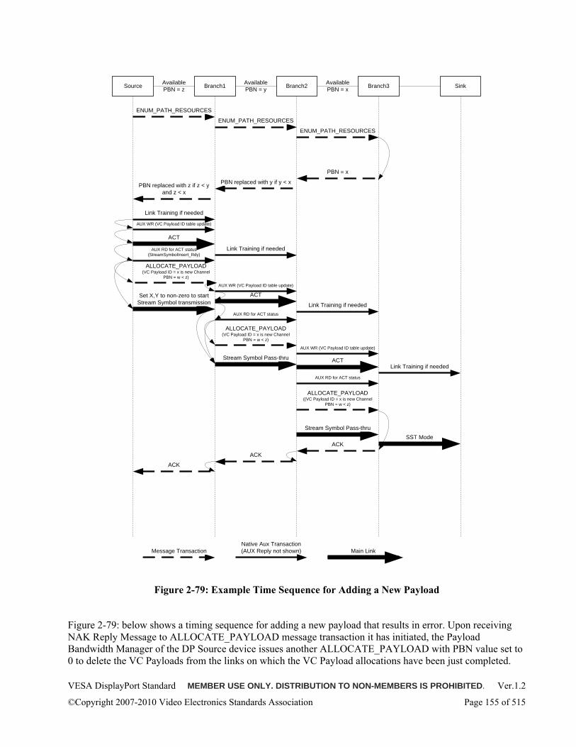
VESA DisplayPort Standard MEMBER USE ONLY. DISTRIBUTION TO NON-MEMBERS IS PROHIBITED. Ver.1.2
©Copyright 2007-2010 Video Electronics Standards Association Page 155 of 515
Source Branch1 Branch2 Sink
ENUM_PATH_RESOURCES
PBN replaced with y if y < x
ENUM_PATH_RESOURCES
PBN replaced with z if z < y and z < x
ALLOCATE_PAYLOAD(VC Payload ID = x is new Channel
PBN = w < z)
ALLOCATE_PAYLOAD(VC Payload ID = x is new Channel
PBN = w < z)
Available PBN = z
Available PBN = y
Available PBN = x
AUX WR (VC Payload ID table update)
ACT
ACK
ACK
Branch3
ALLOCATE_PAYLOAD((VC Payload ID = x is new Channel
PBN = w < z)
ACK
ENUM_PATH_RESOURCES
PBN = x
AUX RD for ACT status(StreamSymbolInsert_Rdy)
Message TransactionNative Aux Transaction(AUX Reply not shown) Main Link
Link Training if needed
Link Training if needed
ACT
ACT
AUX WR (VC Payload ID table update)
AUX RD for ACT status
Link Training if needed
AUX RD for ACT status
Link Training if needed
AUX WR (VC Payload ID table update)
Stream Symbol Pass-thru
Stream Symbol Pass-thru
Set X,Y to non-zero to start Stream Symbol transmission
SST Mode
Figure 2-79: Example Time Sequence for Adding a New Payload
Figure 2-79: below shows a timing sequence for adding a new payload that results in error. Upon receiving NAK Reply Message to ALLOCATE_PAYLOAD message transaction it has initiated, the Payload Bandwidth Manager of the DP Source device issues another ALLOCATE_PAYLOAD with PBN value set to 0 to delete the VC Payloads from the links on which the VC Payload allocations have been just completed.
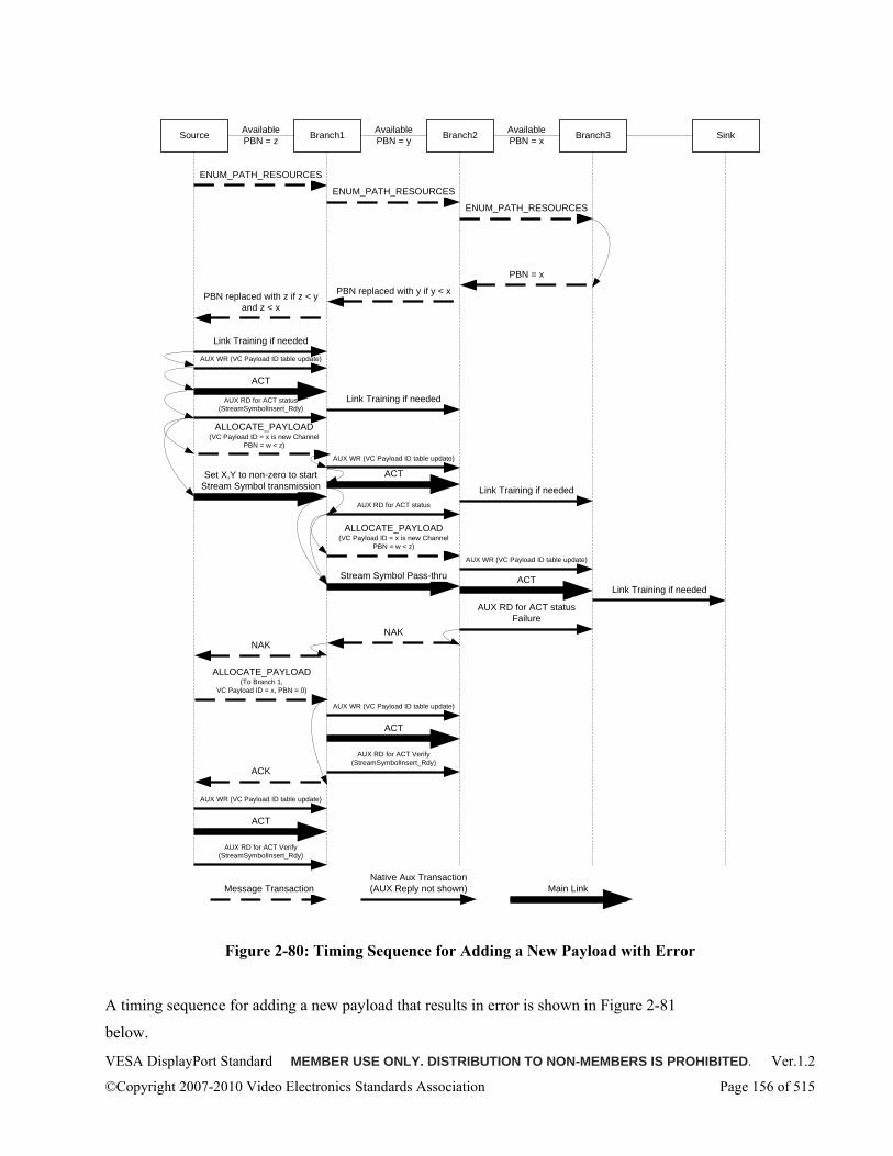
VESA DisplayPort Standard MEMBER USE ONLY. DISTRIBUTION TO NON-MEMBERS IS PROHIBITED. Ver.1.2
©Copyright 2007-2010 Video Electronics Standards Association Page 156 of 515
Source Branch1 Branch2 Sink
ENUM_PATH_RESOURCES
PBN replaced with y if y < x
ENUM_PATH_RESOURCES
PBN replaced with z if z < y and z < x
ALLOCATE_PAYLOAD(VC Payload ID = x is new Channel
PBN = w < z)
ALLOCATE_PAYLOAD(VC Payload ID = x is new Channel
PBN = w < z)
Available PBN = z
Available PBN = y
Available PBN = x
AUX WR (VC Payload ID table update)
ACT
NAKNAK
Branch3
ENUM_PATH_RESOURCES
PBN = x
AUX RD for ACT status(StreamSymbolInsert_Rdy)
Message TransactionNative Aux Transaction(AUX Reply not shown) Main Link
Link Training if needed
Link Training if needed
ACT
ACT
AUX WR (VC Payload ID table update)
AUX RD for ACT status
Link Training if needed
AUX RD for ACT status Failure
Link Training if needed
AUX WR (VC Payload ID table update)
Stream Symbol Pass-thru
Set X,Y to non-zero to start Stream Symbol transmission
ACK
ALLOCATE_PAYLOAD(To Branch 1,
VC Payload ID = x, PBN = 0)
ACT
AUX WR (VC Payload ID table update)
AUX RD for ACT Verify(StreamSymbolInsert_Rdy)
AUX WR (VC Payload ID table update)
ACT
AUX RD for ACT Verify(StreamSymbolInsert_Rdy)
Figure 2-80: Timing Sequence for Adding a New Payload with Error
A timing sequence for adding a new payload that results in error is shown in Figure 2-81
below.
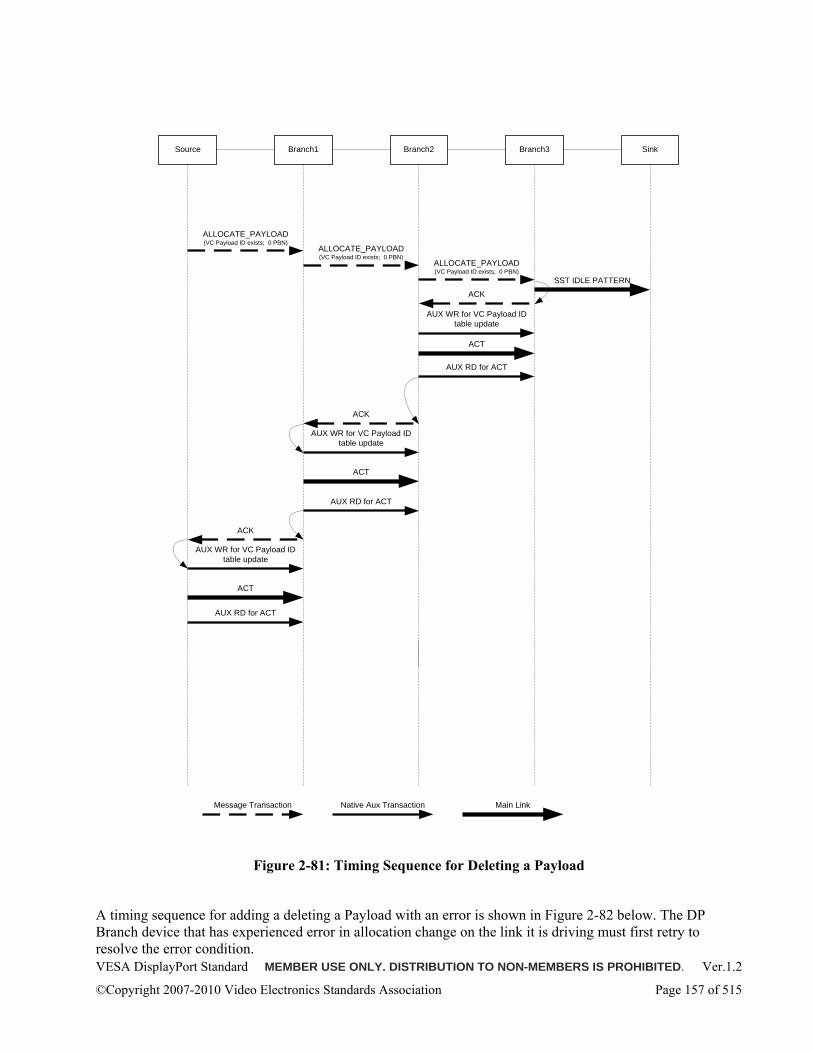
VESA DisplayPort Standard MEMBER USE ONLY. DISTRIBUTION TO NON-MEMBERS IS PROHIBITED. Ver.1.2
©Copyright 2007-2010 Video Electronics Standards Association Page 157 of 515
Source Branch1 Branch2 Sink
ACK
AUX WR for VC Payload ID table update
ACK
AUX WR for VC Payload ID table update
Branch3
ACK
Message Transaction Native Aux Transaction Main Link
ACT
ACT
ACT
ALLOCATE_PAYLOAD(VC Payload ID exists; 0 PBN)
ALLOCATE_PAYLOAD(VC Payload ID exists; 0 PBN)
ALLOCATE_PAYLOAD(VC Payload ID exists; 0 PBN)
AUX RD for ACT
AUX RD for ACT
AUX WR for VC Payload ID table update
AUX RD for ACT
SST IDLE PATTERN
Figure 2-81: Timing Sequence for Deleting a Payload
A timing sequence for adding a deleting a Payload with an error is shown in Figure 2-82 below. The DP Branch device that has experienced error in allocation change on the link it is driving must first retry to resolve the error condition.
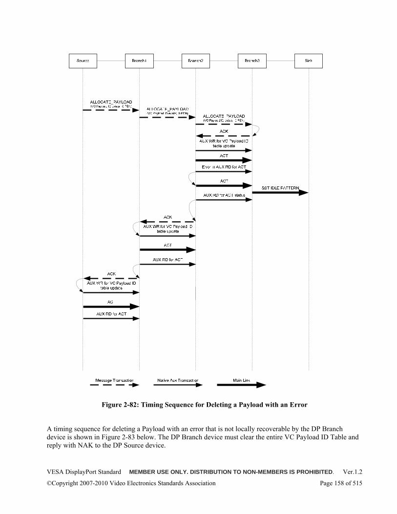
VESA DisplayPort Standard MEMBER USE ONLY. DISTRIBUTION TO NON-MEMBERS IS PROHIBITED. Ver.1.2
©Copyright 2007-2010 Video Electronics Standards Association Page 158 of 515
Figure 2-82: Timing Sequence for Deleting a Payload with an Error
A timing sequence for deleting a Payload with an error that is not locally recoverable by the DP Branch device is shown in Figure 2-83 below. The DP Branch device must clear the entire VC Payload ID Table and reply with NAK to the DP Source device.
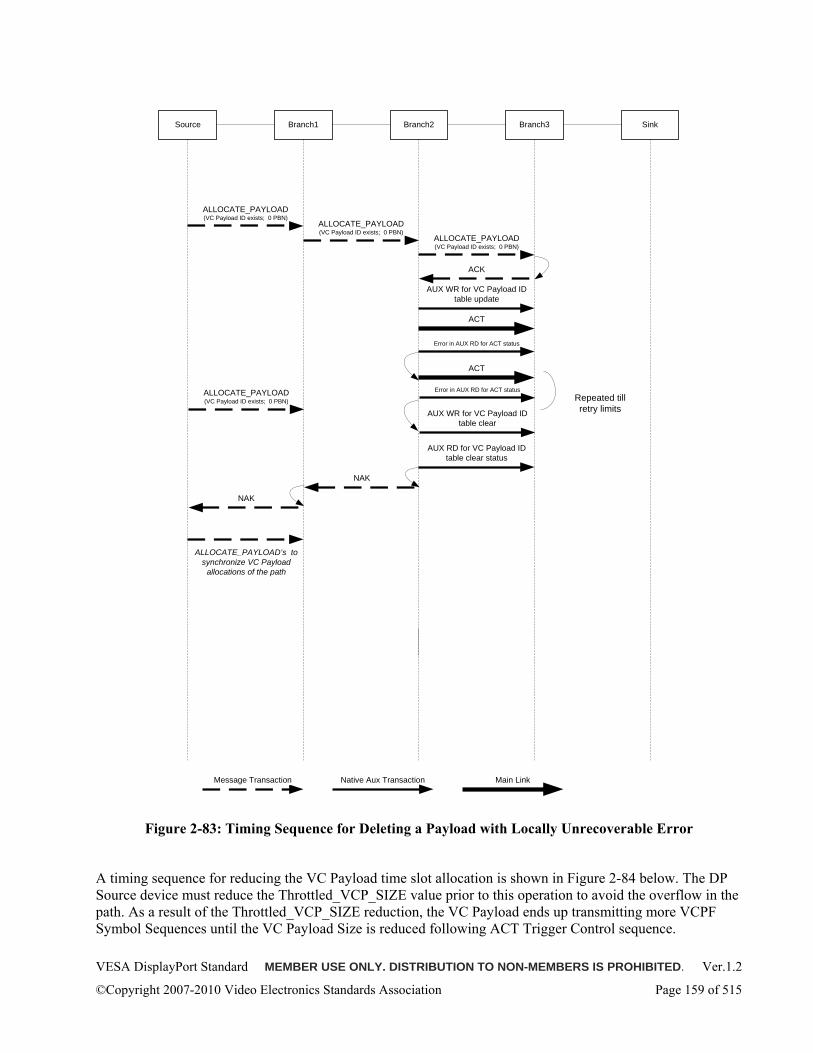
VESA DisplayPort Standard MEMBER USE ONLY. DISTRIBUTION TO NON-MEMBERS IS PROHIBITED. Ver.1.2
©Copyright 2007-2010 Video Electronics Standards Association Page 159 of 515
Source Branch1 Branch2 Sink
NAK
AUX WR for VC Payload ID table update
ACK
Branch3
NAK
Message Transaction Native Aux Transaction Main Link
ACT
ALLOCATE_PAYLOAD(VC Payload ID exists; 0 PBN)
ALLOCATE_PAYLOAD(VC Payload ID exists; 0 PBN)
ALLOCATE_PAYLOAD(VC Payload ID exists; 0 PBN)
Error in AUX RD for ACT status
ACT
Error in AUX RD for ACT statusRepeated till retry limitsAUX WR for VC Payload ID
table clear
AUX RD for VC Payload ID table clear status
ALLOCATE_PAYLOAD(VC Payload ID exists; 0 PBN)
ALLOCATE_PAYLOAD’s to synchronize VC Payload
allocations of the path
Figure 2-83: Timing Sequence for Deleting a Payload with Locally Unrecoverable Error
A timing sequence for reducing the VC Payload time slot allocation is shown in Figure 2-84 below. The DP Source device must reduce the Throttled_VCP_SIZE value prior to this operation to avoid the overflow in the path. As a result of the Throttled_VCP_SIZE reduction, the VC Payload ends up transmitting more VCPF Symbol Sequences until the VC Payload Size is reduced following ACT Trigger Control sequence.
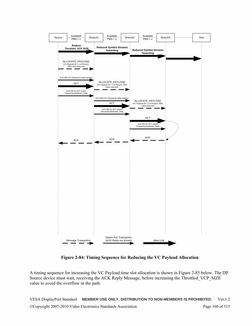
VESA DisplayPort Standard MEMBER USE ONLY. DISTRIBUTION TO NON-MEMBERS IS PROHIBITED. Ver.1.2
©Copyright 2007-2010 Video Electronics Standards Association Page 160 of 515
Source Branch1 Branch2 Sink
ALLOCATE_PAYLOAD(VC Payload ID = x is Present,
PBN value reduced)
Available PBN = z
Available PBN = y
Available PBN = x
AUX WR (VC Payload ID table update)
ACT
ACKACK
Branch3
ACK
AUX RD for ACT status(StreamSymbolInsert_Rdy)
Message TransactionNative Aux Transaction(AUX Reply not shown) Main Link
ACT
ACT
AUX WR (VC Payload ID table update)
AUX RD for ACT status(StreamSymbolInsert_Rdy)
AUX RD for ACT status(StreamSymbolInsert_Rdy)
Reduce Throttled_VCP SIZE Reduced Symbol Streams
fowarding Reduced Symbol Streams fowarding
ALLOCATE_PAYLOAD(VC Payload ID = x is Present, PBN
value reduced)
ALLOCATE_PAYLOAD(VC Payload ID = x is Present, PBN
value reduced)
Figure 2-84: Timing Sequence for Reducing the VC Payload Allocation
A timing sequence for increasing the VC Payload time slot allocation is shown in Figure 2-85 below. The DP Source device must wait, receiving the ACK Reply Message, before increasing the Throttled_VCP_SIZE value to avoid the overflow in the path.
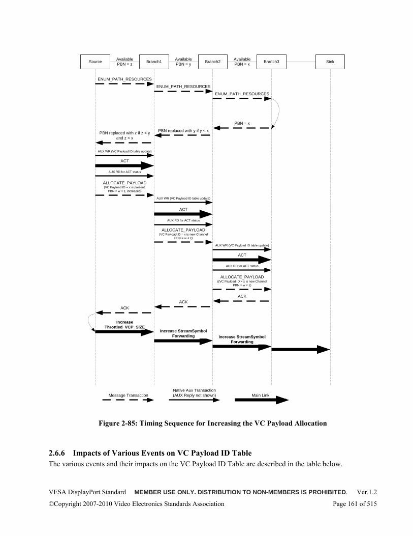
VESA DisplayPort Standard MEMBER USE ONLY. DISTRIBUTION TO NON-MEMBERS IS PROHIBITED. Ver.1.2
©Copyright 2007-2010 Video Electronics Standards Association Page 161 of 515
Source Branch1 Branch2 Sink
ENUM_PATH_RESOURCES
PBN replaced with y if y < x
ENUM_PATH_RESOURCES
PBN replaced with z if z < y and z < x
ALLOCATE_PAYLOAD(VC Payload ID = x is present,
PBN = w < z, increased)
ALLOCATE_PAYLOAD(VC Payload ID = x is new Channel
PBN = w < z)
Available PBN = z
Available PBN = y
Available PBN = x
AUX WR (VC Payload ID table update)
ACT
ACKACK
Branch3
ALLOCATE_PAYLOAD((VC Payload ID = x is new Channel
PBN = w < z)
ACK
ENUM_PATH_RESOURCES
PBN = x
AUX RD for ACT status
Message TransactionNative Aux Transaction(AUX Reply not shown) Main Link
Increase Throttled_VCP_SIZE
ACT
ACT
Increase StreamSymbol Forwarding Increase StreamSymbol
Forwarding
AUX WR (VC Payload ID table update)
AUX RD for ACT status
AUX RD for ACT status
AUX WR (VC Payload ID table update)
Figure 2-85: Timing Sequence for Increasing the VC Payload Allocation
2.6.6 Impacts of Various Events on VC Payload ID Table The various events and their impacts on the VC Payload ID Table are described in the table below.
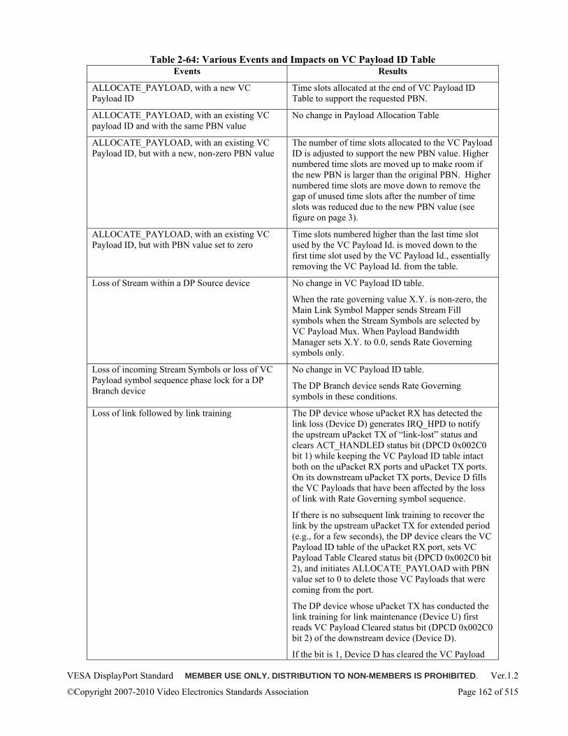
VESA DisplayPort Standard MEMBER USE ONLY. DISTRIBUTION TO NON-MEMBERS IS PROHIBITED. Ver.1.2
©Copyright 2007-2010 Video Electronics Standards Association Page 162 of 515
Table 2-64: Various Events and Impacts on VC Payload ID Table Events Results
ALLOCATE_PAYLOAD, with a new VC Payload ID
Time slots allocated at the end of VC Payload ID Table to support the requested PBN.
ALLOCATE_PAYLOAD, with an existing VC payload ID and with the same PBN value
No change in Payload Allocation Table
ALLOCATE_PAYLOAD, with an existing VC Payload ID, but with a new, non-zero PBN value
The number of time slots allocated to the VC Payload ID is adjusted to support the new PBN value. Higher numbered time slots are moved up to make room if the new PBN is larger than the original PBN. Higher numbered time slots are move down to remove the gap of unused time slots after the number of time slots was reduced due to the new PBN value (see figure on page 3).
ALLOCATE_PAYLOAD, with an existing VC Payload ID, but with PBN value set to zero
Time slots numbered higher than the last time slot used by the VC Payload Id. is moved down to the first time slot used by the VC Payload Id., essentially removing the VC Payload Id. from the table.
Loss of Stream within a DP Source device No change in VC Payload ID table.
When the rate governing value X.Y. is non-zero, the Main Link Symbol Mapper sends Stream Fill symbols when the Stream Symbols are selected by VC Payload Mux. When Payload Bandwidth Manager sets X.Y. to 0.0, sends Rate Governing symbols only.
Loss of incoming Stream Symbols or loss of VC Payload symbol sequence phase lock for a DP Branch device
No change in VC Payload ID table.
The DP Branch device sends Rate Governing symbols in these conditions.
Loss of link followed by link training
The DP device whose uPacket RX has detected the link loss (Device D) generates IRQ_HPD to notify the upstream uPacket TX of “link-lost” status and clears ACT_HANDLED status bit (DPCD 0x002C0 bit 1) while keeping the VC Payload ID table intact both on the uPacket RX ports and uPacket TX ports. On its downstream uPacket TX ports, Device D fills the VC Payloads that have been affected by the loss of link with Rate Governing symbol sequence.
If there is no subsequent link training to recover the link by the upstream uPacket TX for extended period (e.g., for a few seconds), the DP device clears the VC Payload ID table of the uPacket RX port, sets VC Payload Table Cleared status bit (DPCD 0x002C0 bit 2), and initiates ALLOCATE_PAYLOAD with PBN value set to 0 to delete those VC Payloads that were coming from the port.
The DP device whose uPacket TX has conducted the link training for link maintenance (Device U) first reads VC Payload Cleared status bit (DPCD 0x002C0 bit 2) of the downstream device (Device D).
If the bit is 1, Device D has cleared the VC Payload
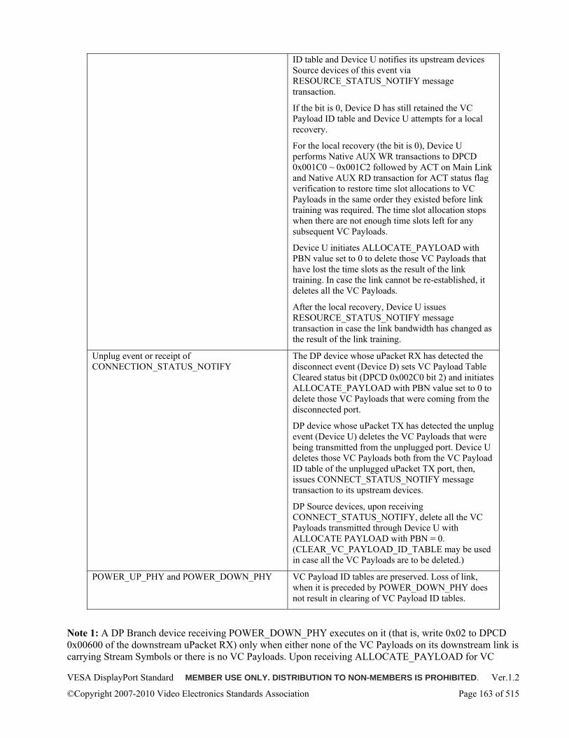
VESA DisplayPort Standard MEMBER USE ONLY. DISTRIBUTION TO NON-MEMBERS IS PROHIBITED. Ver.1.2
©Copyright 2007-2010 Video Electronics Standards Association Page 163 of 515
ID table and Device U notifies its upstream devices Source devices of this event via RESOURCE_STATUS_NOTIFY message transaction.
If the bit is 0, Device D has still retained the VC Payload ID table and Device U attempts for a local recovery.
For the local recovery (the bit is 0), Device U performs Native AUX WR transactions to DPCD 0x001C0 ~ 0x001C2 followed by ACT on Main Link and Native AUX RD transaction for ACT status flag verification to restore time slot allocations to VC Payloads in the same order they existed before link training was required. The time slot allocation stops when there are not enough time slots left for any subsequent VC Payloads.
Device U initiates ALLOCATE_PAYLOAD with PBN value set to 0 to delete those VC Payloads that have lost the time slots as the result of the link training. In case the link cannot be re-established, it deletes all the VC Payloads.
After the local recovery, Device U issues RESOURCE_STATUS_NOTIFY message transaction in case the link bandwidth has changed as the result of the link training.
Unplug event or receipt of CONNECTION_STATUS_NOTIFY
The DP device whose uPacket RX has detected the disconnect event (Device D) sets VC Payload Table Cleared status bit (DPCD 0x002C0 bit 2) and initiates ALLOCATE_PAYLOAD with PBN value set to 0 to delete those VC Payloads that were coming from the disconnected port.
DP device whose uPacket TX has detected the unplug event (Device U) deletes the VC Payloads that were being transmitted from the unplugged port. Device U deletes those VC Payloads both from the VC Payload ID table of the unplugged uPacket TX port, then, issues CONNECT_STATUS_NOTIFY message transaction to its upstream devices.
DP Source devices, upon receiving CONNECT_STATUS_NOTIFY, delete all the VC Payloads transmitted through Device U with ALLOCATE PAYLOAD with PBN = 0. (CLEAR_VC_PAYLOAD_ID_TABLE may be used in case all the VC Payloads are to be deleted.)
POWER_UP_PHY and POWER_DOWN_PHY VC Payload ID tables are preserved. Loss of link, when it is preceded by POWER_DOWN_PHY does not result in clearing of VC Payload ID tables.
Note 1: A DP Branch device receiving POWER_DOWN_PHY executes on it (that is, write 0x02 to DPCD 0x00600 of the downstream uPacket RX) only when either none of the VC Payloads on its downstream link is carrying Stream Symbols or there is no VC Payloads. Upon receiving ALLOCATE_PAYLOAD for VC
VESA DisplayPort Standard MEMBER USE ONLY. DISTRIBUTION TO NON-MEMBERS IS PROHIBITED. Ver.1.2
©Copyright 2007-2010 Video Electronics Standards Association Page 164 of 515
Payload allocation through the link on which POWER_DOWN_PHY has been executed, the DP Branch device must execute POWER_UP_PHY (that is, write 0x01 to DPCD 0x00600).
Note 2: Power cycling of the uPacket TX of an upstream DP device is detected by the uPacket RX of the downstream DP device as a loss of link without preceding POWR_DOWN_PHY and is handled as such.
Note 3: Power cycling of the uPacket RX of a downstream DP device is detected by the uPacket TX of the upstream DP device as an unplug event and is handled as such.
2.6.7 Robustness Requirement There are four aspects to the robustness of the MST mode.
o Link timing robustness through predictable, self-generated link timing
o Trigger Control Sequence robustness in MTP Header time slots
o VC Payload 4-symbol sequence phase locking
o VC Payload symbol robustness through redundancy in symbol transmission, regardless of the lane count.
This section describes the uPacket RX implementation requirements for utilizing the above aspects for improved robustness of the link.
2.6.7.1 Link Timing Robustness uPacket TX must maintain the 216 symbol interval of SR in MST mode following the establishment of Main Link via Link Training.
uPacket RX must make sure the consistency of SR interval before using the SR symbol as the link timing reference point. Besides, uPacket RX must disregard the appearance of SR symbol at an unexpected time slot which may result from an intermittent symbol error over Main Link. The uPacket RX must wait for four consecutive SRs with 216 time-slot intervals before switching to an SR location different from the original location.
2.6.7.2 Trigger Control Sequence Robustness in MTP Header Time Slot Since the location of Trigger Control Sequence such as ACT Trigger Sequence is unpredictable, other than it is inserted in MTP Header time slots, uPacket TX sends 4-symbol sequence per lane on four consecutive MTP Header time slots.
uPacket RX must use this 4-symbol sequence redundancy to properly detect the Trigger Control Sequence even when two out of the four Control Symbols have errors.
2.6.7.3 VC Payload 4-Symbol Sequence Boundary Establishment uPacket RX must establish the 4-symbol sequence boundary and must correct symbols that do not match the Stream Control Symbol Sequence/Rate Governing Symbol Sequence rule.
2.6.7.4 Stream Framing Symbol Sequence Robustness Stream Framing Symbol Sequence, namely, each of BS, BE, SS, and SE consists of four consecutive, identical Control Codes. Majority voting after ANSI8B/10B decoding must be used for the robustness. The uPacket RX must pick the Control Code that appears in two or more symbols in the 4-symbol sequence.
2.6.8 Control Functions, Control Symbols and K-Code Assignment Control Functions consist of sets of defined control symbols or sequences, and are used in both Main Link Symbol Management and VC Payload Mapping Layers. To improve link integrity, MST uses 4-symbol sequences to identify all the Data Symbols and those Control Symbols that appear in VC Payload time slots. To minimize emission effects of these 4-symbol codes, the underlying K-codes used are selected using a
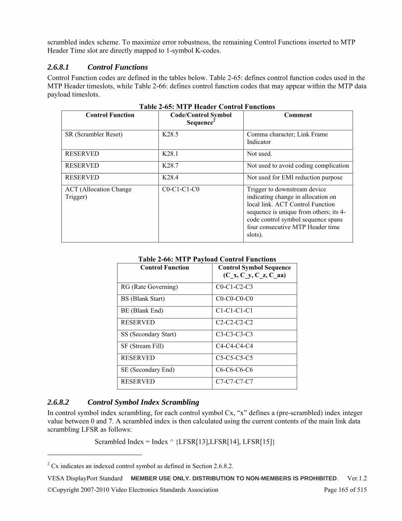
VESA DisplayPort Standard MEMBER USE ONLY. DISTRIBUTION TO NON-MEMBERS IS PROHIBITED. Ver.1.2
©Copyright 2007-2010 Video Electronics Standards Association Page 165 of 515
scrambled index scheme. To maximize error robustness, the remaining Control Functions inserted to MTP Header Time slot are directly mapped to 1-symbol K-codes.
2.6.8.1 Control Functions Control Function codes are defined in the tables below. Table 2-65: defines control function codes used in the MTP Header timeslots, while Table 2-66: defines control function codes that may appear within the MTP data payload timeslots.
Table 2-65: MTP Header Control Functions Control Function Code/Control Symbol
Sequence2 Comment
SR (Scrambler Reset) K28.5 Comma character; Link Frame Indicator
RESERVED K28.1 Not used.
RESERVED K28.7 Not used to avoid coding complication
RESERVED K28.4 Not used for EMI reduction purpose
ACT (Allocation Change Trigger)
C0-C1-C1-C0 Trigger to downstream device indicating change in allocation on local link. ACT Control Function sequence is unique from others; its 4-code control symbol sequence spans four consecutive MTP Header time slots).
Table 2-66: MTP Payload Control Functions Control Function Control Symbol Sequence
(C_x, C_y, C_z, C_aa)
RG (Rate Governing) C0-C1-C2-C3
BS (Blank Start) C0-C0-C0-C0
BE (Blank End) C1-C1-C1-C1
RESERVED C2-C2-C2-C2
SS (Secondary Start) C3-C3-C3-C3
SF (Stream Fill) C4-C4-C4-C4
RESERVED C5-C5-C5-C5
SE (Secondary End) C6-C6-C6-C6
RESERVED C7-C7-C7-C7
2.6.8.2 Control Symbol Index Scrambling In control symbol index scrambling, for each control symbol Cx, “x” defines a (pre-scrambled) index integer value between 0 and 7. A scrambled index is then calculated using the current contents of the main link data scrambling LFSR as follows:
Scrambled Index = Index ^ LFSR[13],LFSR[14], LFSR[15]
2 Cx indicates an indexed control symbol as defined in Section 2.6.8.2.
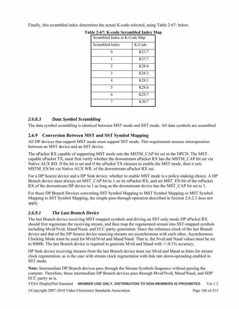
VESA DisplayPort Standard MEMBER USE ONLY. DISTRIBUTION TO NON-MEMBERS IS PROHIBITED. Ver.1.2
©Copyright 2007-2010 Video Electronics Standards Association Page 166 of 515
Finally, this scrambled index determines the actual K-code selected, using Table 2-67: below.
Table 2-67: K-code Scrambled Index Map Scrambled Index to K-Code Map
Scrambled Index K-Code
0 K23.7
1 K27.7
2 K28.0
3 K28.2
4 K28.3
5 K28.6
6 K29.7
7 K30.7
2.6.8.3 Data Symbol Scrambling The data symbol scrambling is identical between MST mode and SST mode. All data symbols are scrambled.
2.6.9 Conversion Between MST and SST Symbol Mapping All DP devices that support MST mode must support SST mode. This requirement ensures interoperation between an MST device and an SST device.
The uPacket RX capable of supporting MST mode sets the MSTM_CAP bit set in the DPCD. The MST-capable uPacket TX, must first verify whether the downstream uPacket RX has the MSTM_CAP bit set via Native AUX RD. If the bit is set and if the uPacket TX chooses to enable the MST mode, then it sets MSTM_EN bit via Native AUX WR. of the downstream uPacket RX set,
For a DP Source device and a DP Sink device, whether to enable MST mode is a policy-making choice. A DP Branch device must always set MST_CAP bit to 1 on its mPacket RX, and set MST_EN bit of the mPacket RX of the downstream DP device to 1 as long as the downstream device has the MST_CAP bit set to 1.
For those DP Branch Devices converting SST Symbol Mapping to MST Symbol Mapping or MST Symbol Mapping to SST Symbol Mapping, the simple pass-through operation described in Section 2.6.2.3 does not apply.
2.6.9.1 The Last Branch Device The last Branch device receiving MST-mapped symbols and driving an SST-only mode DP uPacket RX should first regenerate the receiving stream, and then map the regenerated stream into SST-mapped symbols including Mvid/Nvid, Maud/Naud, and ECC parity generation. Since the reference clock of the last Branch device and that of the DP Source device sourcing streams are asynchronous with each other, Asynchronous Clocking Mode must be used for Mvid/Nvid and Maud/Naud. That is, the Nvid and Naud values must be set to 8000h. The last Branch device is required to generate Mvid and Maud with +/-0.1% accuracy.
DP Sink device receiving streams from the last Branch device must use Mvid and Maud as hints for stream clock regeneration, as is the case with stream clock regeneration with link rate down-spreading enabled in SST mode.
Note: Intermediate DP Branch devices pass through the Stream Symbols Sequence without parsing the contents. Therefore, those intermediate DP Branch devices pass through Mvid/Nvid, Maud/Naud, and SDP ECC parity as is.
VESA DisplayPort Standard MEMBER USE ONLY. DISTRIBUTION TO NON-MEMBERS IS PROHIBITED. Ver.1.2
©Copyright 2007-2010 Video Electronics Standards Association Page 167 of 515
There may be ways to simplify the conversion from MST symbol mapping to SST symbol mapping, but it is an implementation-specific choice and is outside the scope of this Standard.
2.6.9.1.1 Enablement of Enhanced Framing Symbol Sequence by the Last Branch Device The last Branch device driving the downstream device in SST mode must enable the Enhanced Framing Symbol Sequence as long as the downstream device is capable of the Enhanced Framing Symbol Sequence.
2.6.9.2 The First Branch Device The first Branch device receiving SST-mapped symbols from an SST-only mode Source device must forward the stream to the downstream link in SST transport format with the same link configuration as the upstream link.
When an upstream Source device is MST-capable, but chooses to transmit in SST format, the MST Source device must initiate ALLOCATE_PAYLOAD message transaction to establish the virtual channel to the target Sink device. In this case, the first Branch device converts incoming SST-mapped symbols into MST-mapped symbols including Mvid/Nvid, Maud/Naud, and ECC parity generation. Since the reference clock of the last Branch device and that of the DP Source device sourcing streams are asynchronous with each other, Asynchronous Clocking Mode must be used for Mvid/Nvid and Maud/Naud.
There may be ways to simplify this conversion, but it is an implementation-specific choice and outside the scope of this standard
2.6.9.2.1 Enhanced Framing Symbol Sequence support by the First Branch Device The first Branch device must support the Enhanced Framing Symbol Sequence in SST mode.
2.6.9.3 Mode Switching between MST Mode and SST Mode The uPacket TX and RX capable of MST mode must support SST mode to interoperate with SST-only mode DP Devices.
Switching between MST mode and SST mode results in interruption of the transport of stream(s) as the uPacket TX must stop the stream transport prior to this mode switch. There are two options as follows:
The uPacket TX reinitiates Link Training, and come out of the Link Training with Idle Pattern in SST mode or no-VC Payload (that is, empty MTP) pattern in MST mode.
The uPacket TX stops the transport of streams (resulting in IDLE PATTERN in SST mode or no VC Payload, or empty MTP, in MST mode), sets/clears MST_EN bit via Native AUX WR depending on the direction of the mode switch, and switches the Main Link pattern at BS (for SST-to-MST mode switch) or at SR (for MST-to-SST mode switch). Starting of a stream transport or a VC Payload allocation must wait at least four BS intervals (after switching to SST mode) or four SR intervals (after switching to MST mode).
2.6.10 MTPH Usages for CP Extension in MST Mode Two additional usages of MTPH time slots are defined for CP Extension in MST mode: Encryption Control Field and Link Verification Pattern (LVP).
2.6.10.1 Encryption Control Field The Encryption Control Field (ECF) consists of an eight data symbol sequence spanning eight consecutive MTPHs. The data symbol sequence is identical per-lane, regardless of lane count. The ECF is repeated four consecutive times, resulting in a total sequence length of 32 MTPs. The uPacket RX is required to apply majority voting on the repeated ECF’s for error correction.
How the ECF is used is specific to Content Protection system ported onto MST DP link and is therefore outside the scope of DP Standard.
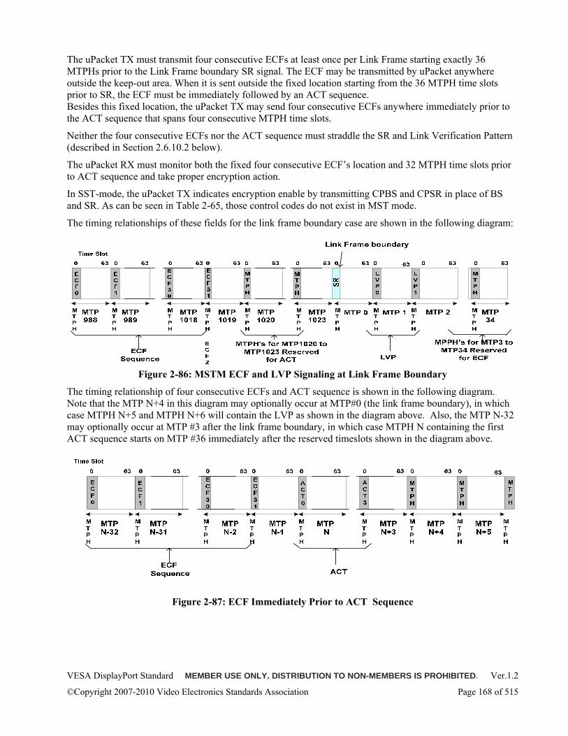
VESA DisplayPort Standard MEMBER USE ONLY. DISTRIBUTION TO NON-MEMBERS IS PROHIBITED. Ver.1.2
©Copyright 2007-2010 Video Electronics Standards Association Page 168 of 515
The uPacket TX must transmit four consecutive ECFs at least once per Link Frame starting exactly 36 MTPHs prior to the Link Frame boundary SR signal. The ECF may be transmitted by uPacket anywhere outside the keep-out area. When it is sent outside the fixed location starting from the 36 MTPH time slots prior to SR, the ECF must be immediately followed by an ACT sequence. Besides this fixed location, the uPacket TX may send four consecutive ECFs anywhere immediately prior to the ACT sequence that spans four consecutive MTPH time slots.
Neither the four consecutive ECFs nor the ACT sequence must straddle the SR and Link Verification Pattern (described in Section 2.6.10.2 below).
The uPacket RX must monitor both the fixed four consecutive ECF’s location and 32 MTPH time slots prior to ACT sequence and take proper encryption action.
In SST-mode, the uPacket TX indicates encryption enable by transmitting CPBS and CPSR in place of BS and SR. As can be seen in Table 2-65, those control codes do not exist in MST mode.
The timing relationships of these fields for the link frame boundary case are shown in the following diagram:
Figure 2-86: MSTM ECF and LVP Signaling at Link Frame Boundary
The timing relationship of four consecutive ECFs and ACT sequence is shown in the following diagram. Note that the MTP N+4 in this diagram may optionally occur at MTP#0 (the link frame boundary), in which case MTPH N+5 and MTPH N+6 will contain the LVP as shown in the diagram above. Also, the MTP N-32 may optionally occur at MTP #3 after the link frame boundary, in which case MTPH N containing the first ACT sequence starts on MTP #36 immediately after the reserved timeslots shown in the diagram above.
Figure 2-87: ECF Immediately Prior to ACT Sequence
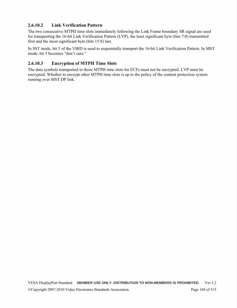
VESA DisplayPort Standard MEMBER USE ONLY. DISTRIBUTION TO NON-MEMBERS IS PROHIBITED. Ver.1.2
©Copyright 2007-2010 Video Electronics Standards Association Page 169 of 515
2.6.10.2 Link Verification Pattern The two consecutive MTPH time slots immediately following the Link Frame boundary SR signal are used for transporting the 16-bit Link Verification Pattern (LVP), the least significant byte (bits 7:0) transmitted first and the most significant byte (bits 15:8) last.
In SST mode, bit 5 of the VBID is used to sequentially transport the 16-bit Link Verification Pattern. In MST mode, bit 5 becomes “don’t care.”
2.6.10.3 Encryption of MTPH Time Slots The data symbols transported in those MTPH time slots for ECFs must not be encrypted. LVP must be encrypted. Whether to encrypt other MTPH time slots is up to the policy of the content protection system running over MST DP link.
VESA DisplayPort Standard MEMBER USE ONLY. DISTRIBUTION TO NON-MEMBERS IS PROHIBITED. Ver.1.2
©Copyright 2007-2010 Video Electronics Standards Association Page 170 of 515
2.7 AUX Transaction Syntax in Manchester Transaction Format The syntaxes used for various AUX transactions in Manchester transaction format are described in this section. As described in Section 3.4, the Manchester transaction format uses Manchester-II coding at the nominal bit rate of 1Mbps.
The following two categories are explained:
• Native AUX transaction syntax
• Syntax for mapping of an I2C onto AUX transaction called I2C-over-AUX transaction
This section describes the DisplayPort AUX transaction syntax suitable for a half-duplex, bidirectional AUX CH PHY. The number of bus turn-around is reduced to minimize the half-duplex overhead.
The AUX CH PHY consists of a single differential pair carrying self-clocking data. All transactions must start with a preamble "SYNC" for synchronizing the Requester (uPacket TX) and the Replier (uPacket TX), and must end with a "STOP" condition.
A 4-bit command, COMM3:0, must be transmitted after the preamble, followed by a 20-bit address, ADDR19:0. The DisplayPort capability, status and control functions are directly mapped to the 20-bit address space. In addition, DisplayPort uses these 20 bits to access I2C devices.
After the transmission of command and address, the data bytes must be transmitted except for Address-only transaction for I2C-over-AUX transaction. Burst data transfer is supported. The burst data size must be limited to a maximum of 16 bytes.
Bit 3 (msb) of the request command field indicates whether the transaction is a Native AUX transaction or an I2C-over-AUX transaction.
VESA DisplayPort Standard MEMBER USE ONLY. DISTRIBUTION TO NON-MEMBERS IS PROHIBITED. Ver.1.2
©Copyright 2007-2010 Video Electronics Standards Association Page 171 of 515
Table 2-68: Bit/Byte Size of Various Data Types of AUX Transaction Syntax
Data Type Bit Width
Command 4 bits Request transaction: 20 bits Address Reply transaction: None (0000b must be padded to Command to form a byte) Request transaction:
For read: 1Byte (Length byte) For write: 1Byte (Length byte) + N Data Bytes
o Length byte (“LEN”) defines the number of bytes to be written to or to be read from the AUX Replier (uPacket RX) by the AUX Requester (uPacket TX).
o N = Integer value from 1 to 16. That is, a uPacket TX is required to limit the burst data size to 16 or fewer bytes.
Data
Reply transaction: For read = N Data bytes.
o N = Integer value from 1 to 16, the number of bytes ready to be sent. For write = 0 or 1 Data byte
o When AUX Replier NACK’s the write request transaction, it must indicate how many bytes have been written.
o For an I2C write over the AUX CH, the AUX Replier, following the ACK, must indicate how many bytes have been written to the I2C slave.
Note: In the document, "" is attached to a signal name that is driven by the Requester, while "" is attached to a signal driven by the Replier.
2.7.1 Command definition Request and reply command definitions of AUX transactions are described in this section.
2.7.1.1 Request command definition Bit 3 = Native AUX or I2C-over-AUX
1 = DisplayPort transaction
0 = I2C transaction
• When bit 3 = 1 (Native AUX transaction):
o Bits 2:0 = Request type
000 = Write
001= Read
• When bit 3 = 0 (I2C-over-AUX transaction):
o Bit 2 = MOT (Middle-of-Transaction) bit.
o Bits 1:0 = I2C_Command
00 = Write
01 = Read
10 = Write_Status_Update_Request
VESA DisplayPort Standard MEMBER USE ONLY. DISTRIBUTION TO NON-MEMBERS IS PROHIBITED. Ver.1.2
©Copyright 2007-2010 Video Electronics Standards Association Page 172 of 515
11 = Reserved
Note: More on MOT bit and I2C Write Status Request in Section 2.7.5 and Section 2.7.7.
2.7.1.2 Reply Command Definition The 4-bit Reply Command field is divided into Native AUX Reply field (bits 1:0) and I2C-over-AUX Reply field (bits 3:2). The I2C-over-AUX Reply field is valid only when Native AUX Reply field is AUX_ACK (00). When Native AUX Reply field is not 00, then, I2C-over-AUX Reply field must be 00 and be ignored.
Bits 1:0 = Native AUX Reply field
00 = AUX_ACK
• For Write transaction: All the data bytes have been written.
• For Read transaction: Ready to reply to Read request with data following.
o A uPacket RX (Replier) may assert a STOP condition before transmitting the total number of requested data bytes when not all the bytes are available.
01 = AUX NACK
• For Write transaction:
o AUX NACK must be followed by a data byte “M”, where “M” indicates the number of data bytes successfully written.
o When a uPacket TX is writing a DPCD address not supported by the uPacket RX, the uPacket RX shall reply with AUX NACK and “M” equal to zero.
• For Read transaction: o A uPacket RX receiving a Native AUX RD request for an unsupported DPCD address must
reply with an AUX ACK and read data set equal to zero instead of replying with AUX NACK.
10 = AUX DEFER
• For Write and Read transactions:
o Not ready for the write/read request. A uPacket TX may retry later
11 = Reserved
Bits3:2 = I2C-over-AUX Reply field
A uPacket RX must not forward an I2C transaction to an I2C slave unless the AUX CH has received all the data bytes. When the uPacket TX fails to receive all the data bytes it either AUX NACKs (with “M” set equal to the number of received data bytes) or AUX DEFERs (not ready to receive the request transaction). The DisplayPort uPacket TX may either abort the I2C-over-AUX transaction or retry at a later time.
I2C-over-AUX Reply field is only valid when paired with AUX ACK.
00 = I2C ACK
• For I2C write transactions:
o I2C ACK must be followed by the data byte “M” where “M” is the number of bytes the uPacket RX has written to its I2C slave without NACK. The data byte “M” must be omitted when all the data bytes have been written. See Section 2.7.5.2 for examples.
• For I2C read transactions:
VESA DisplayPort Standard MEMBER USE ONLY. DISTRIBUTION TO NON-MEMBERS IS PROHIBITED. Ver.1.2
©Copyright 2007-2010 Video Electronics Standards Association Page 173 of 515
o The I2C slave has ACKed the I2C address and the uPacket RX is ready to reply with data following.
o The uPacket RX may assert a STOP condition before transmitting the total number of requested data bytes when not all the bytes are available.
01 = I2C NACK
• For I2C Write transaction:
o I2C NACK must be followed by a data byte “M” except when the I2C slave has NACK’ed the I2C address, in which case the reply transaction shall end with I2C NACK without the data byte “M”. The data byte “M” indicates the number of bytes the uPacket RX has successfully written to its I2C slave before getting the NACK. The byte on which the NACK occurred is excluded from the number.
• For I2C Read transaction:
o The I2C slave has NACKed the I2C address.
10 = I2C DEFER
• For I2C write and read transactions:
o The I2C slave has yet to ACK or NACK the I2C transaction.
11 = Reserved
2.7.2 AUX Transaction Response/Reply Time-outs AUX Replier (the uPacket RX) must start sending the reply back to the AUX requester (the uPacket TX) within the response period of 300μs. The timer for Response Time-out starts ticking after the uPacket RX has finished receiving the AUX STOP condition which ends the AUX Request transaction.
The timer is reset either when the Response Time-out period has elapsed or when the uPacket RX has started to send the AUX Sync pattern (which follows 10 to 16 active pre-charge pulses) for the Reply transaction.
If the uPacket TX does not receive a reply from the uPacket RX it must wait for a Reply Time-out period of 400us before initiating the next AUX Request transaction. The timer for the Reply Time-out starts ticking after the uPacket TX has finished sending the AUX STOP condition.
The timer is reset either when the Reply Time-out period elapses or when the uPacket TX detects the first zero in Manchester-II code which is in active pre-charge pulses and AUX Sync pattern of the Reply transaction.
2.7.3 Native AUX Request Transaction Syntax SYNC COMM3:0|ADDR19:16 ADDR15:8 ADDR7:0 LEN7:0 (DATA0-7:0 ...) STOP
2.7.3.1 Write Request Transaction For write transaction (COMM3:0 = 1000), the Request transaction must stop when the number of bytes (1 - 16 = LEN7:0 value + 1, all other values are invalid) has been transmitted from the Requester to the Replier.
2.7.3.2 Read Request Transaction For read transaction (COMM3:0 = 1001), the Request transaction must stop after LEN7:0. That is, no data must be transmitted. The Requester expects the Replier to reply with [LEN7:0 value + 1] bytes (= 1 - 16 bytes) of data.
VESA DisplayPort Standard MEMBER USE ONLY. DISTRIBUTION TO NON-MEMBERS IS PROHIBITED. Ver.1.2
©Copyright 2007-2010 Video Electronics Standards Association Page 174 of 515
2.7.4 Native AUX Reply Transaction Syntax SYNC COMM3:0|0000 (DATA0-7:0...) STOP
2.7.4.1 Reply Transaction to Write Request A reply transaction to a write request must end in one of the three conditions below:
• The Replier has received a write request, and has completed the write. The Replier must reply to the transaction by sending AUXACK.
o SYNC 00|AUX ACK|0000 STOP,
• The Replier has received a write request, but has not completed the write. The Replier must end the transaction by sending AUX NACK as the first COMM3:0, and then, the number of written bytes M as DATA0_7:0.
o SYNC 00| NACK|0000 DATA0_7:0 STOP,
Where DATA0-7:0 shows the number of written bytes, M
• Replier has received a write request, but is not ready to accept the write request. Replier must reply with AUX_DEFER. o SYNC 00|AUX_DEFER|0000 STOP
2.7.4.2 Reply Transaction to a Read Request A reply transaction to a Read request must end in one of the four conditions below:
• The Replier has received a read request, but is not ready to reply with the read data. Must end the transaction by sending AUX DEFER as the first COMM3:0.
o SYNC 00|AUX DEFER|0000 STOP
• The Replier has received a read request and is ready. Must reply by sending AUX ACK as the first command, transmit back the number of requested bytes, assert the STOP condition, and release the AUX CH.
o SYNC 00|AUX ACK|0000 STOP
• The Replier has received a read request and is ready with some (M+1 bytes) but not all, of requested data bytes. Must reply by sending AUX ACK as the first command, transmit back the number of bytes that can be replied, assert the STOP condition, and release the AUX CH.
o SYNC 00|AUX ACK|0000 DATA0_7:0... DATAM_7:0STOP
• The Replier has received a read request for N bytes and is ready. Must reply with AUX ACK as the first command, transmit back the number of requested bytes, assert STOP condition, and then release the AUX CH.
o SYNC 00|AUX ACK|0000 DATA0_7:0... DATAN-1_7:0 STOP
2.7.5 I2C Bus Transaction Mapping onto AUX Syntax The mapping of an I2C transaction onto the I2C-over-AUX transactions as defined in the DisplayPort Standard is agnostic to the application-specific usage of the I2C data bytes. Neither the uPacket TX nor the uPacket RX must be aware of how each of the data bytes in the I2C transaction is used for a specific I2C application.
A single I2C transaction may be mapped onto one or multiple I2C-over-AUX transactions to accommodate the bit-rate difference between I2C and AUX CH. How (or whether) to divide an I2C transaction into multiple I2C-over-AUX transactions is specific to the implementation of uPacket TX. For an I2C-over-AUX
VESA DisplayPort Standard MEMBER USE ONLY. DISTRIBUTION TO NON-MEMBERS IS PROHIBITED. Ver.1.2
©Copyright 2007-2010 Video Electronics Standards Association Page 175 of 515
transaction, a uPacket TX may initiate an “Address-only” request transaction in which the uPacket TX will STOP the AUX transaction after sending the Request command field and 20-bit Address without sending LENGTH byte/data bytes.
2.7.5.1 I2C-over-AUX Request Transaction Command When bit 3 (msb) of the Request command is 0, the requested transaction must be an I2C-over-AUX transaction. A single I2C transaction may be divided into multiple I2C-over-AUX transactions, each with bit 3 of the Request command set to 0.
In an I2C bus transaction, the remaining three bits of the Request command are defined as follows:
• Bit 2 = MOT (Middle-of-Transaction) bit.
o This bit must be set when the I2C transaction does not end (or STOP) with the current AUX transaction. The I2C master in the uPacket RX must send the seven bit I2C address and read or write command only when:
MOT bit is set to 1 for the first time, that is, in the first AUX transaction for the START of an I2C transaction,
Or
RepeatedStart is issued, which results either in a new I2C address or the same I2C address but with the read/write command opposite of the previous command.
• Bits 1:0 = I2C Command
o 00 = Write
o 01 = Read
o 10 = Write_Status_Update_Request
When the last I2C write transaction resulted in a reply of either I2C_DEFER or ACK followed by a data byte M where M is the number of bytes written to the I2C slave, AUX Requester (uPacket TX) may issue the following special request to inquire the status of the last I2C write:
SYNC COM3:0 (= 0110)|0000 0000|0000 0|7-bit I2C address (the same as the last) 0000|0000 (Length byte) STOP
To this request, AUX Replier (uPacket RX) must reply with the latest status.
o 11 = RESERVED
2.7.5.2 I2C Write Transaction In this section, mapping of an I2C Write transaction onto the AUX transaction(s) is described using an example in which three data bytes are written. An I2C master in the Source device will initiate an I2C Write transaction to an I2C slave in a Sink device via the AUX CH between uPacket TX in the Source device and uPacket RX in the Sink device as shown in Figure 2-88. Three variants of the operation are shown, demonstrating a variety of ways to accomplish the goal of performing an I2C Write transaction.
In the following descriptions, the I2C slave in the Sink device acknowledges the I2C Write. When the I2C slave non-acknowledges the I2C write (either I2C address is not supported or the write data byte is not accepted), what corrective action to take is up to the I2C master in the Source device and beyond the scope of this Standard.
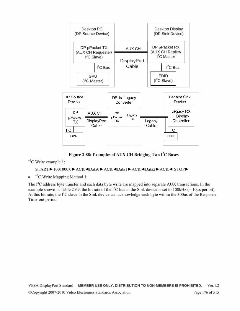
VESA DisplayPort Standard MEMBER USE ONLY. DISTRIBUTION TO NON-MEMBERS IS PROHIBITED. Ver.1.2
©Copyright 2007-2010 Video Electronics Standards Association Page 176 of 515
DP Packet TX(AUX CH Requester/
I2C Slave)
Desktop PC(DP Source Device)
DisplayPortCable
Desktop Display(DP Sink Device)
DP Packet RX (AUX CH Replier/
I2C Master
EDID(I2C Slave)
GPU(I2C Master)
I2C Bus I2C Bus
AUX CH
Figure 2-88: Examples of AUX CH Bridging Two I2C Buses
I2C Write example 1:
START1001000|0ACKData0ACKData1ACKData2ACK STOP
• I2C Write Mapping Method 1:
The I2C address byte transfer and each data byte write are mapped into separate AUX transactions. In the example shown in Table 2-69, the bit rate of the I2C bus in the Sink device is set to 100kHz (= 10μs per bit). At this bit rate, the I2C slave in the Sink device can acknowledge each byte within the 300us of the Response Time-out period.
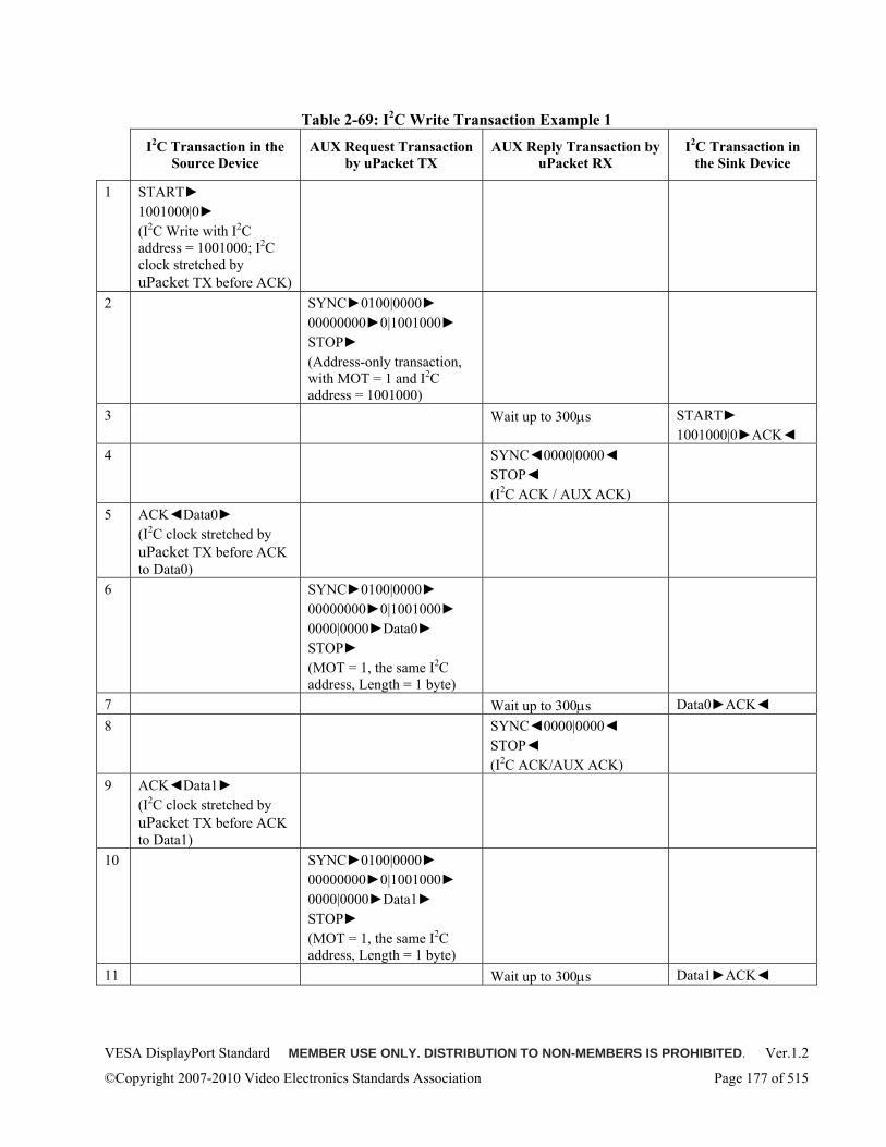
VESA DisplayPort Standard MEMBER USE ONLY. DISTRIBUTION TO NON-MEMBERS IS PROHIBITED. Ver.1.2
©Copyright 2007-2010 Video Electronics Standards Association Page 177 of 515
Table 2-69: I2C Write Transaction Example 1 I2C Transaction in the
Source Device AUX Request Transaction
by uPacket TX AUX Reply Transaction by
uPacket RX I2C Transaction in
the Sink Device
1 START 1001000|0 (I2C Write with I2C address = 1001000; I2C clock stretched by uPacket TX before ACK)
2 SYNC0100|0000 000000000|1001000 STOP (Address-only transaction, with MOT = 1 and I2C address = 1001000)
3 Wait up to 300μs START 1001000|0ACK
4 SYNC0000|0000 STOP (I2C ACK / AUX ACK)
5 ACKData0 (I2C clock stretched by uPacket TX before ACK to Data0)
6 SYNC0100|0000 000000000|1001000 0000|0000Data0 STOP (MOT = 1, the same I2C address, Length = 1 byte)
7 Wait up to 300μs Data0ACK 8 SYNC0000|0000
STOP (I2C ACK/AUX ACK)
9 ACKData1 (I2C clock stretched by uPacket TX before ACK to Data1)
10 SYNC0100|0000 000000000|1001000 0000|0000Data1 STOP (MOT = 1, the same I2C address, Length = 1 byte)
11 Wait up to 300μs Data1ACK
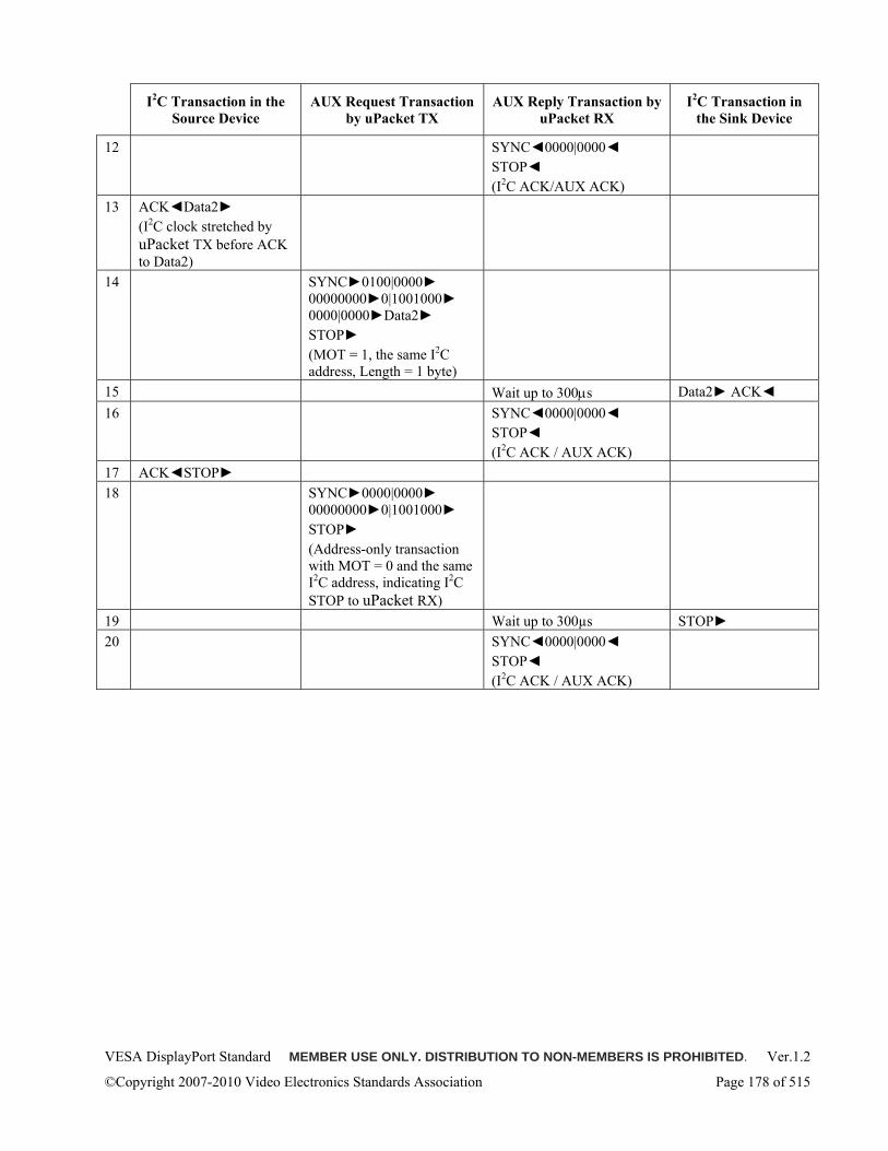
VESA DisplayPort Standard MEMBER USE ONLY. DISTRIBUTION TO NON-MEMBERS IS PROHIBITED. Ver.1.2
©Copyright 2007-2010 Video Electronics Standards Association Page 178 of 515
I2C Transaction in the Source Device
AUX Request Transaction by uPacket TX
AUX Reply Transaction by uPacket RX
I2C Transaction in the Sink Device
12 SYNC0000|0000 STOP (I2C ACK/AUX ACK)
13 ACKData2 (I2C clock stretched by uPacket TX before ACK to Data2)
14 SYNC0100|0000 000000000|1001000 0000|0000Data2 STOP (MOT = 1, the same I2C address, Length = 1 byte)
15 Wait up to 300μs Data2 ACK 16 SYNC0000|0000
STOP (I2C ACK / AUX ACK)
17 ACKSTOP 18 SYNC0000|0000
000000000|1001000 STOP (Address-only transaction with MOT = 0 and the same I2C address, indicating I2C STOP to uPacket RX)
19 Wait up to 300µs STOP 20 SYNC0000|0000
STOP (I2C ACK / AUX ACK)
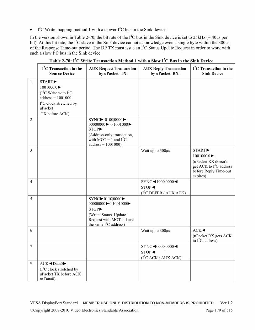
VESA DisplayPort Standard MEMBER USE ONLY. DISTRIBUTION TO NON-MEMBERS IS PROHIBITED. Ver.1.2
©Copyright 2007-2010 Video Electronics Standards Association Page 179 of 515
• I2C Write mapping method 1 with a slower I2C bus in the Sink device:
In the version shown in Table 2-70, the bit rate of the I2C bus in the Sink device is set to 25kHz (= 40us per bit). At this bit rate, the I2C slave in the Sink device cannot acknowledge even a single byte within the 300us of the Response Time-out period. The DP TX must issue an I2C Status Update Request in order to work with such a slow I2C bus in the Sink device.
Table 2-70: I2C Write Transaction Method 1 with a Slow I2C Bus in the Sink Device
I2C Transaction in the Source Device
AUX Request Transaction by uPacket TX
AUX Reply Transaction by uPacket RX
I2C Transaction in the Sink Device
1 START 1001000|0 (I2C Write with I2C address = 1001000; I2C clock stretched by uPacket TX before ACK)
2 SYNC 0100|0000 00000000 0|1001000 STOP (Address-only transaction, with MOT = 1 and I2C address = 1001000)
3 Wait up to 300μs START 1001000|0 (uPacket RX doesn’t get ACK to I2C address before Reply Time-out expires)
4 SYNC1000|0000 STOP (I2C DEFER / AUX ACK)
5 SYNC0110|0000 000000000|1001000 STOP (Write_Status_Update_ Request with MOT = 1 and the same I2C address)
6 Wait up to 300μs ACK (uPacket RX gets ACK to I2C address)
7 SYNC0000|0000 STOP (I2C ACK / AUX ACK)
8 ACKData0 (I2C clock stretched by uPacket TX before ACK to Data0)
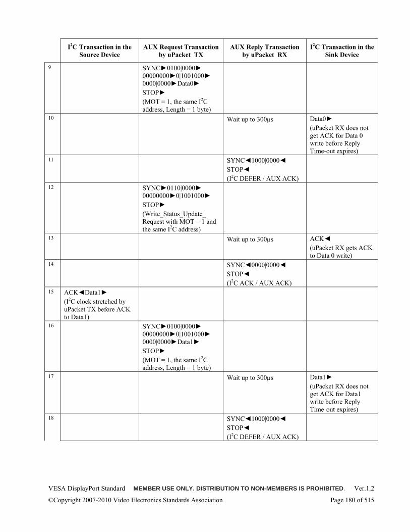
VESA DisplayPort Standard MEMBER USE ONLY. DISTRIBUTION TO NON-MEMBERS IS PROHIBITED. Ver.1.2
©Copyright 2007-2010 Video Electronics Standards Association Page 180 of 515
I2C Transaction in the Source Device
AUX Request Transaction by uPacket TX
AUX Reply Transaction by uPacket RX
I2C Transaction in the Sink Device
9 SYNC0100|0000 000000000|1001000 0000|0000Data0 STOP (MOT = 1, the same I2C address, Length = 1 byte)
10 Wait up to 300μs Data0 (uPacket RX does not get ACK for Data 0 write before Reply Time-out expires)
11 SYNC1000|0000 STOP (I2C DEFER / AUX ACK)
12 SYNC0110|0000 000000000|1001000 STOP (Write_Status_Update_ Request with MOT = 1 and the same I2C address)
13 Wait up to 300μs ACK (uPacket RX gets ACK to Data 0 write)
14 SYNC0000|0000 STOP (I2C ACK / AUX ACK)
15 ACKData1 (I2C clock stretched by uPacket TX before ACK to Data1)
16 SYNC0100|0000 000000000|1001000 0000|0000Data1 STOP (MOT = 1, the same I2C address, Length = 1 byte)
17 Wait up to 300μs Data1 (uPacket RX does not get ACK for Data1 write before Reply Time-out expires)
18 SYNC1000|0000 STOP (I2C DEFER / AUX ACK)
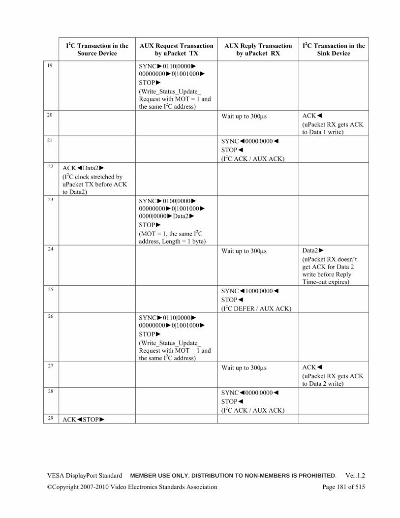
VESA DisplayPort Standard MEMBER USE ONLY. DISTRIBUTION TO NON-MEMBERS IS PROHIBITED. Ver.1.2
©Copyright 2007-2010 Video Electronics Standards Association Page 181 of 515
I2C Transaction in the Source Device
AUX Request Transaction by uPacket TX
AUX Reply Transaction by uPacket RX
I2C Transaction in the Sink Device
19 SYNC0110|0000 000000000|1001000 STOP (Write_Status_Update_ Request with MOT = 1 and the same I2C address)
20 Wait up to 300μs ACK (uPacket RX gets ACK to Data 1 write)
21 SYNC0000|0000 STOP (I2C ACK / AUX ACK)
22 ACKData2 (I2C clock stretched by uPacket TX before ACK to Data2)
23 SYNC0100|0000 000000000|1001000 0000|0000Data2 STOP (MOT = 1, the same I2C address, Length = 1 byte)
24 Wait up to 300μs Data2 (uPacket RX doesn’t get ACK for Data 2 write before Reply Time-out expires)
25 SYNC1000|0000 STOP (I2C DEFER / AUX ACK)
26 SYNC0110|0000 000000000|1001000 STOP (Write_Status_Update_ Request with MOT = 1 and the same I2C address)
27 Wait up to 300μs ACK (uPacket RX gets ACK to Data 2 write)
28 SYNC0000|0000 STOP (I2C ACK / AUX ACK)
29 ACKSTOP
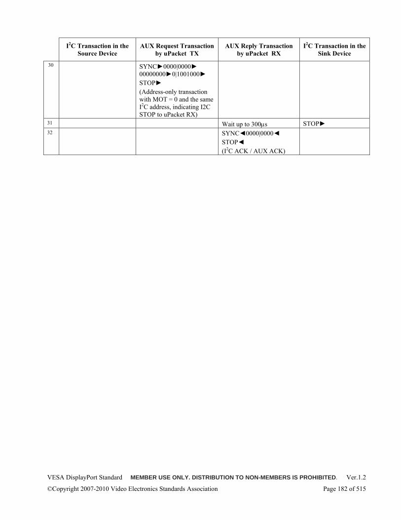
VESA DisplayPort Standard MEMBER USE ONLY. DISTRIBUTION TO NON-MEMBERS IS PROHIBITED. Ver.1.2
©Copyright 2007-2010 Video Electronics Standards Association Page 182 of 515
I2C Transaction in the Source Device
AUX Request Transaction by uPacket TX
AUX Reply Transaction by uPacket RX
I2C Transaction in the Sink Device
30 SYNC0000|0000 000000000|1001000 STOP (Address-only transaction with MOT = 0 and the same I2C address, indicating I2C STOP to uPacket RX)
31 Wait up to 300μs STOP 32 SYNC0000|0000
STOP (I2C ACK / AUX ACK)
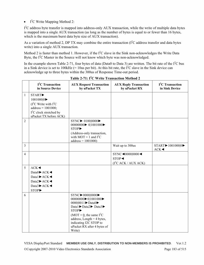
VESA DisplayPort Standard MEMBER USE ONLY. DISTRIBUTION TO NON-MEMBERS IS PROHIBITED. Ver.1.2
©Copyright 2007-2010 Video Electronics Standards Association Page 183 of 515
• I2C Write Mapping Method 2:
I2C address byte transfer is mapped into address-only AUX transaction, while the write of multiple data bytes is mapped into a single AUX transaction (as long as the number of bytes is equal to or fewer than 16 bytes, which is the maximum burst data byte size of AUX transaction).
As a variation of method 2, DP TX may combine the entire transaction (I2C address transfer and data bytes write) into a single AUX transaction.
Method 2 is faster than method 1. However, if the I2C slave in the Sink non-acknowledges the Write Data Byte, the I2C Master in the Source will not know which byte was non-acknowledged.
In the example shown Table 2-71, four bytes of data (Data0 to Data 3) are written. The bit rate of the I2C bus in a Sink device is set to 100kHz (= 10us per bit). At this bit rate, the I2C slave in the Sink device can acknowledge up to three bytes within the 300us of Response Time-out period.
Table 2-71: I2C Write Transaction Method 2
I2C Transaction in Source Device
AUX Request Transaction by uPacket TX
AUX Reply Transaction by uPacket RX
I2C Transaction in Sink Device
1 START 1001000|0 (I2C Write with I2C address = 1001000; I2C clock stretched by uPacket TX before ACK)
2 SYNC 0100|0000 00000000 0|1001000 STOP (Address-only transaction, with MOT = 1 and I2C address = 1001000)
3 Wait up to 300us START1001000|0ACK
4 SYNC0000|0000 STOP (I2C ACK / AUX ACK)
5 ACK Data0ACK Data1ACK Data2ACK Data3ACK STOP
6 SYNC0000|0000 000000000|1001000 0000|0011Data0 Data1Data2 Data3 STOP (MOT = 0, the same I2C address, Length = 4 bytes, indicating I2C STOP to uPacket RX after 4 bytes of Write)
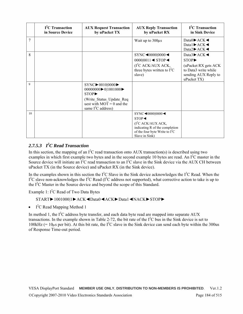
VESA DisplayPort Standard MEMBER USE ONLY. DISTRIBUTION TO NON-MEMBERS IS PROHIBITED. Ver.1.2
©Copyright 2007-2010 Video Electronics Standards Association Page 184 of 515
I2C Transaction in Source Device
AUX Request Transaction by uPacket TX
AUX Reply Transaction by uPacket RX
I2C Transaction in Sink Device
7 Wait up to 300μs Data0ACK Data1ACK Data2ACK
8 SYNC0000|0000 0000|0011 STOP (I2C ACK/AUX ACK, three bytes written to I2C slave)
Data3ACK STOP (uPacket RX gets ACK to Data3 write while sending AUX Reply to uPacket TX)
9 SYNC0010|0000 000000000|1001000 STOP (Write_Status_Update_Request with MOT = 0 and the same I2C address)
10 SYNC0000|0000 STOP (I2C ACK/AUX ACK, indicating R of the completion of the four byte Write to I2C Slave in Sink)
2.7.5.3 I2C Read Transaction In this section, the mapping of an I2C read transaction onto AUX transaction(s) is described using two examples in which first example two bytes and in the second example 10 bytes are read. An I2C master in the Source device will initiate an I2C read transaction to an I2C slave in the Sink device via the AUX CH between uPacket TX (in the Source device) and uPacket RX (in the Sink device).
In the examples shown in this section the I2C Slave in the Sink device acknowledges the I2C Read. When the I2C slave non-acknowledges the I2C Read (I2C address not supported), what corrective action to take is up to the I2C Master in the Source device and beyond the scope of this Standard.
Example 1: I2C Read of Two Data Bytes
START1001000|1ACKData0ACKData1NACKSTOP
• I2C Read Mapping Method 1
In method 1, the I2C address byte transfer, and each data byte read are mapped into separate AUX transactions. In the example shown in Table 2-72, the bit rate of the I2C bus in the Sink device is set to 100kHz (= 10μs per bit). At this bit rate, the I2C slave in the Sink device can send each byte within the 300us of Response Time-out period.
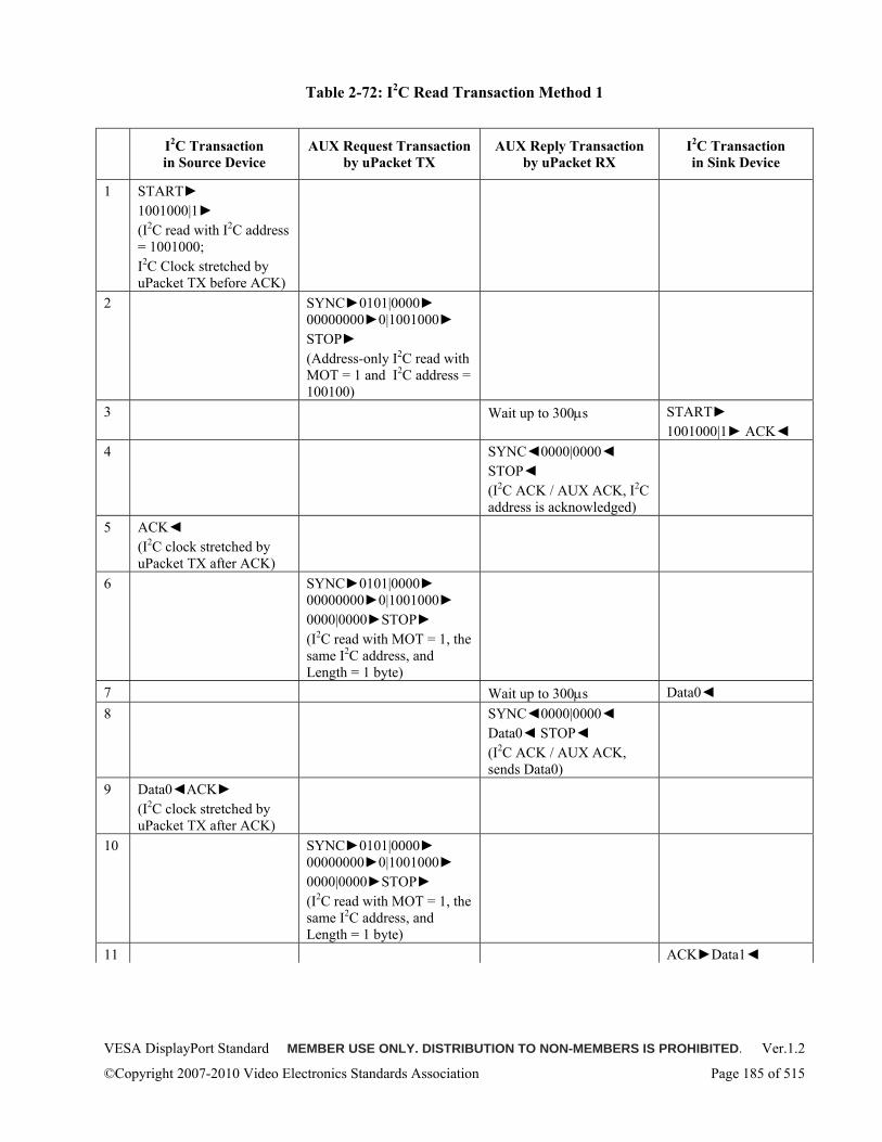
VESA DisplayPort Standard MEMBER USE ONLY. DISTRIBUTION TO NON-MEMBERS IS PROHIBITED. Ver.1.2
©Copyright 2007-2010 Video Electronics Standards Association Page 185 of 515
Table 2-72: I2C Read Transaction Method 1
I2C Transaction in Source Device
AUX Request Transaction by uPacket TX
AUX Reply Transaction by uPacket RX
I2C Transaction in Sink Device
1 START 1001000|1 (I2C read with I2C address = 1001000; I2C Clock stretched by uPacket TX before ACK)
2 SYNC0101|0000 000000000|1001000 STOP (Address-only I2C read with MOT = 1 and I2C address = 100100)
3 Wait up to 300μs START 1001000|1 ACK
4 SYNC0000|0000 STOP (I2C ACK / AUX ACK, I2C address is acknowledged)
5 ACK (I2C clock stretched by uPacket TX after ACK)
6 SYNC0101|0000 000000000|1001000 0000|0000STOP (I2C read with MOT = 1, the same I2C address, and Length = 1 byte)
7 Wait up to 300μs Data0 8 SYNC0000|0000
Data0 STOP (I2C ACK / AUX ACK, sends Data0)
9 Data0ACK (I2C clock stretched by uPacket TX after ACK)
10 SYNC0101|0000 000000000|1001000 0000|0000STOP (I2C read with MOT = 1, the same I2C address, and Length = 1 byte)
11 ACKData1
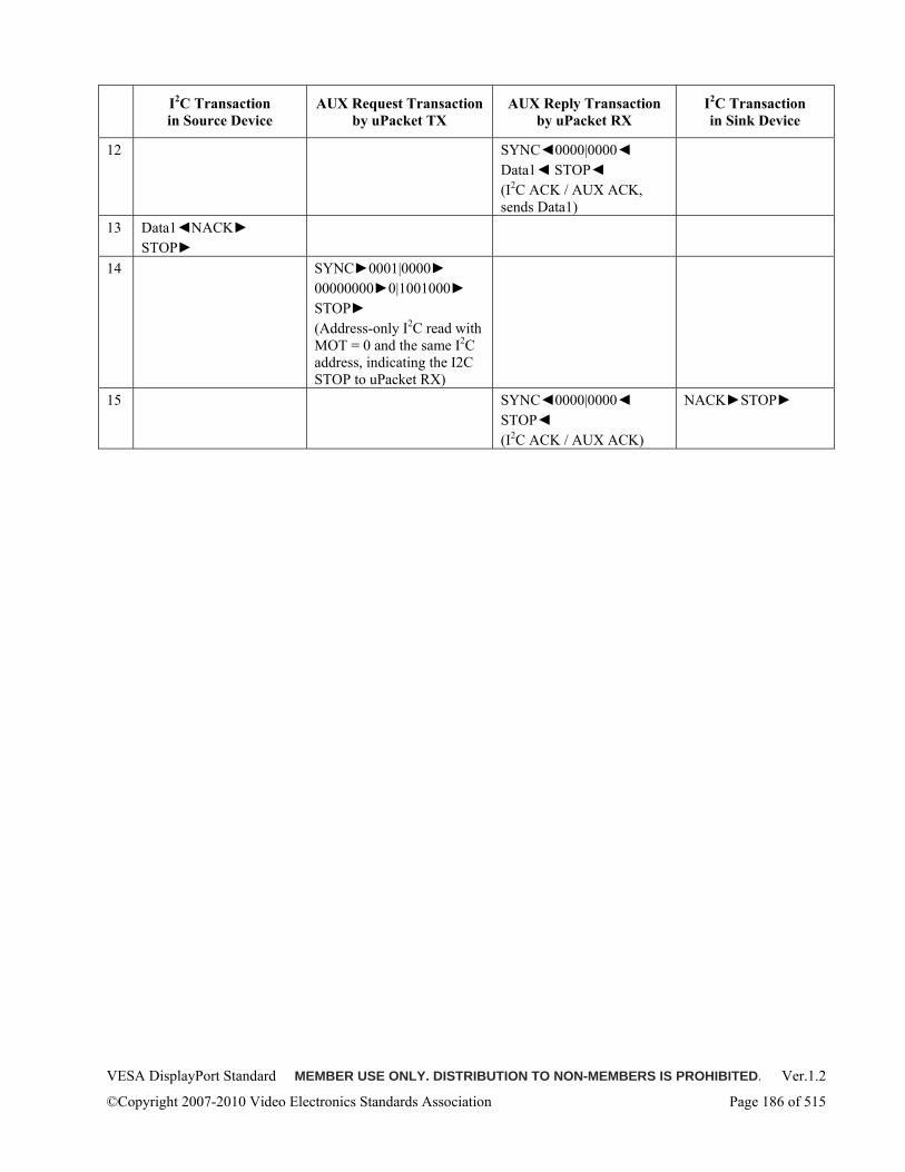
VESA DisplayPort Standard MEMBER USE ONLY. DISTRIBUTION TO NON-MEMBERS IS PROHIBITED. Ver.1.2
©Copyright 2007-2010 Video Electronics Standards Association Page 186 of 515
I2C Transaction in Source Device
AUX Request Transaction by uPacket TX
AUX Reply Transaction by uPacket RX
I2C Transaction in Sink Device
12 SYNC0000|0000 Data1 STOP (I2C ACK / AUX ACK, sends Data1)
13 Data1NACK STOP
14 SYNC0001|0000 000000000|1001000 STOP (Address-only I2C read with MOT = 0 and the same I2C address, indicating the I2C STOP to uPacket RX)
15 SYNC0000|0000 STOP (I2C ACK / AUX ACK)
NACKSTOP
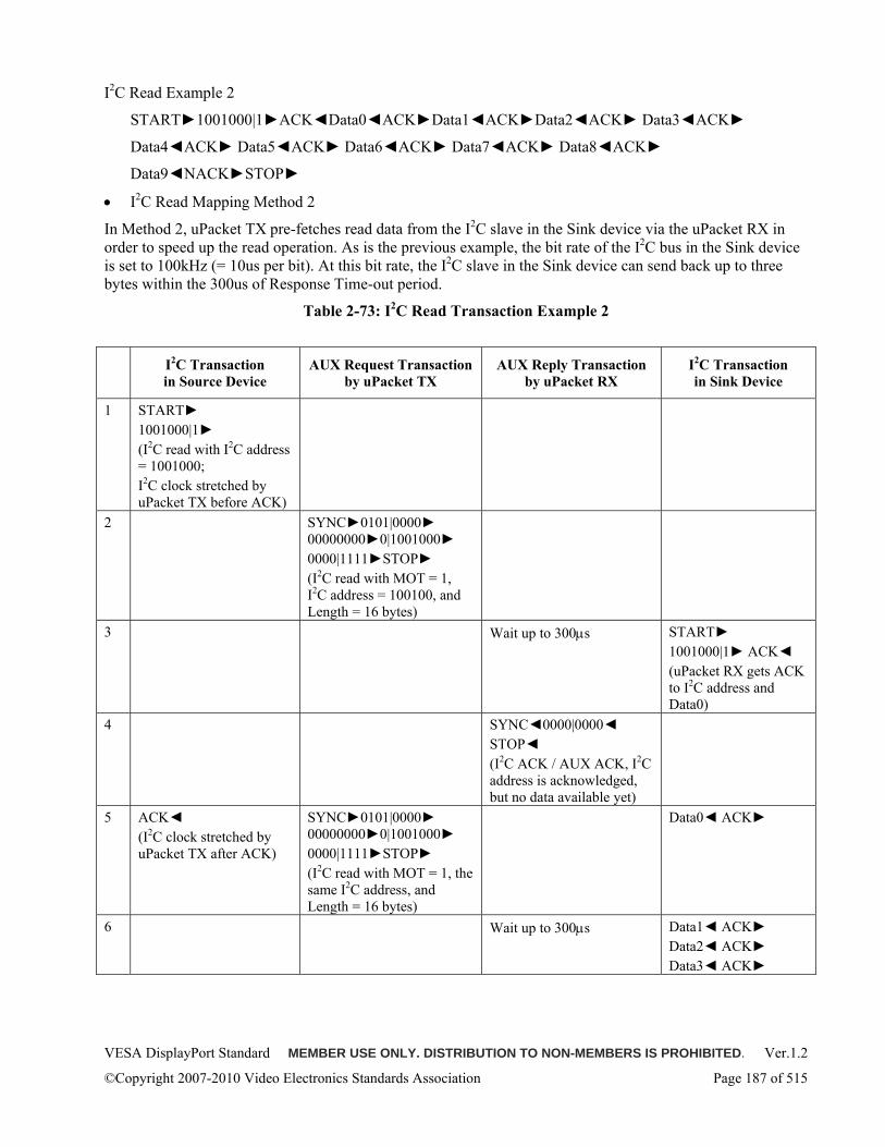
VESA DisplayPort Standard MEMBER USE ONLY. DISTRIBUTION TO NON-MEMBERS IS PROHIBITED. Ver.1.2
©Copyright 2007-2010 Video Electronics Standards Association Page 187 of 515
I2C Read Example 2
START1001000|1ACKData0ACKData1ACKData2ACK Data3ACK
Data4ACK Data5ACK Data6ACK Data7ACK Data8ACK
Data9NACKSTOP
• I2C Read Mapping Method 2
In Method 2, uPacket TX pre-fetches read data from the I2C slave in the Sink device via the uPacket RX in order to speed up the read operation. As is the previous example, the bit rate of the I2C bus in the Sink device is set to 100kHz (= 10us per bit). At this bit rate, the I2C slave in the Sink device can send back up to three bytes within the 300us of Response Time-out period.
Table 2-73: I2C Read Transaction Example 2
I2C Transaction in Source Device
AUX Request Transaction by uPacket TX
AUX Reply Transaction by uPacket RX
I2C Transaction in Sink Device
1 START 1001000|1 (I2C read with I2C address = 1001000; I2C clock stretched by uPacket TX before ACK)
2 SYNC0101|0000 000000000|1001000 0000|1111STOP (I2C read with MOT = 1, I2C address = 100100, and Length = 16 bytes)
3 Wait up to 300μs START 1001000|1 ACK (uPacket RX gets ACK to I2C address and Data0)
4 SYNC0000|0000 STOP (I2C ACK / AUX ACK, I2C address is acknowledged, but no data available yet)
5 ACK (I2C clock stretched by uPacket TX after ACK)
SYNC0101|0000 000000000|1001000 0000|1111STOP (I2C read with MOT = 1, the same I2C address, and Length = 16 bytes)
Data0 ACK
6 Wait up to 300μs Data1 ACK Data2 ACK Data3 ACK
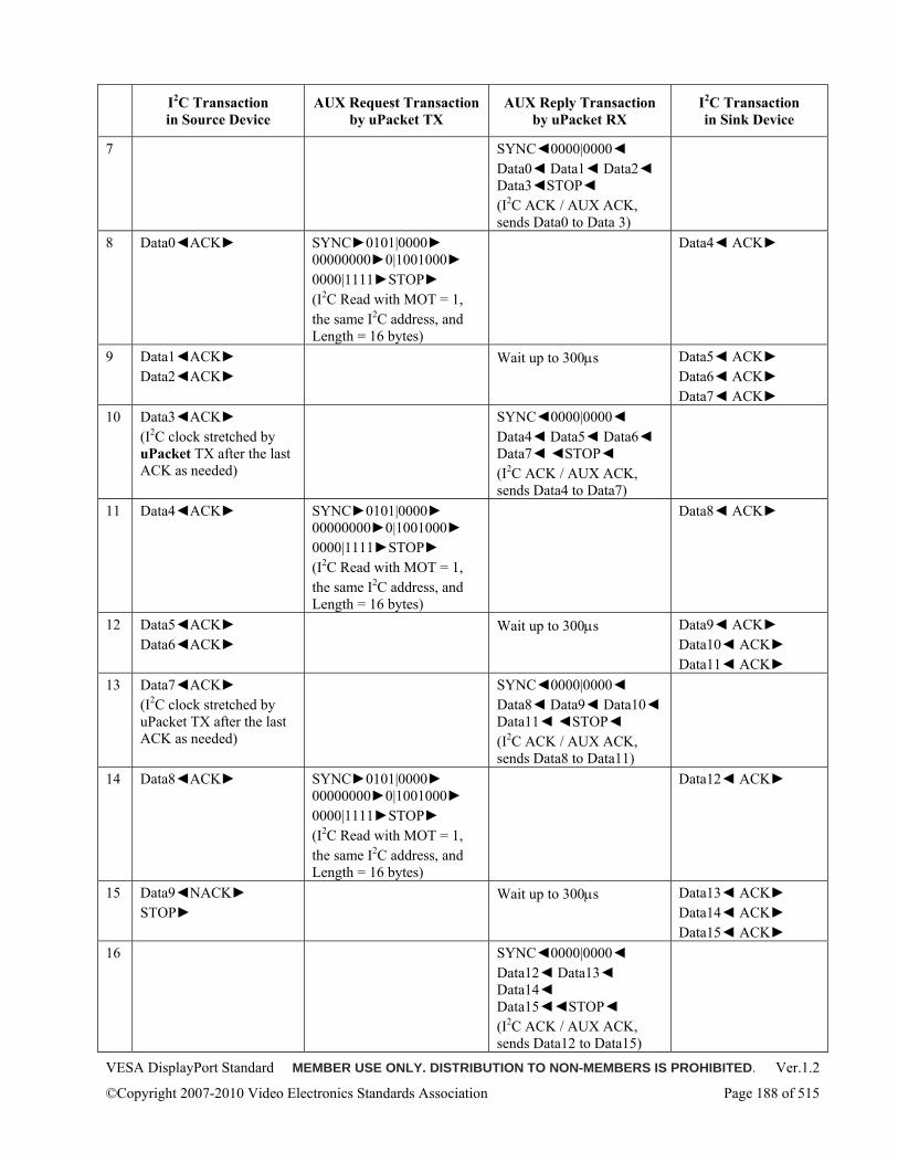
VESA DisplayPort Standard MEMBER USE ONLY. DISTRIBUTION TO NON-MEMBERS IS PROHIBITED. Ver.1.2
©Copyright 2007-2010 Video Electronics Standards Association Page 188 of 515
I2C Transaction in Source Device
AUX Request Transaction by uPacket TX
AUX Reply Transaction by uPacket RX
I2C Transaction in Sink Device
7 SYNC0000|0000 Data0 Data1 Data2 Data3STOP (I2C ACK / AUX ACK, sends Data0 to Data 3)
8 Data0ACK SYNC0101|0000 000000000|1001000 0000|1111STOP (I2C Read with MOT = 1, the same I2C address, and Length = 16 bytes)
Data4 ACK
9 Data1ACK Data2ACK
Wait up to 300μs Data5 ACK Data6 ACK Data7 ACK
10 Data3ACK (I2C clock stretched by uPacket TX after the last ACK as needed)
SYNC0000|0000 Data4 Data5 Data6 Data7 STOP (I2C ACK / AUX ACK, sends Data4 to Data7)
11 Data4ACK SYNC0101|0000 000000000|1001000 0000|1111STOP (I2C Read with MOT = 1, the same I2C address, and Length = 16 bytes)
Data8 ACK
12 Data5ACK Data6ACK
Wait up to 300μs Data9 ACK Data10 ACK Data11 ACK
13 Data7ACK (I2C clock stretched by uPacket TX after the last ACK as needed)
SYNC0000|0000 Data8 Data9 Data10 Data11 STOP (I2C ACK / AUX ACK, sends Data8 to Data11)
14 Data8ACK SYNC0101|0000 000000000|1001000 0000|1111STOP (I2C Read with MOT = 1, the same I2C address, and Length = 16 bytes)
Data12 ACK
15 Data9NACK STOP
Wait up to 300μs Data13 ACK Data14 ACK Data15 ACK
16 SYNC0000|0000 Data12 Data13 Data14 Data15STOP (I2C ACK / AUX ACK, sends Data12 to Data15)
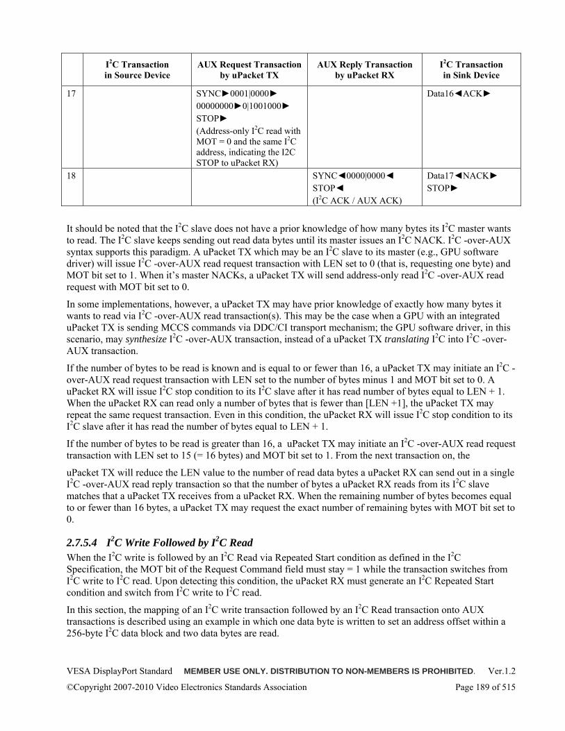
VESA DisplayPort Standard MEMBER USE ONLY. DISTRIBUTION TO NON-MEMBERS IS PROHIBITED. Ver.1.2
©Copyright 2007-2010 Video Electronics Standards Association Page 189 of 515
I2C Transaction in Source Device
AUX Request Transaction by uPacket TX
AUX Reply Transaction by uPacket RX
I2C Transaction in Sink Device
17 SYNC0001|0000 000000000|1001000 STOP (Address-only I2C read with MOT = 0 and the same I2C address, indicating the I2C STOP to uPacket RX)
Data16ACK
18 SYNC0000|0000 STOP (I2C ACK / AUX ACK)
Data17NACK STOP
It should be noted that the I2C slave does not have a prior knowledge of how many bytes its I2C master wants to read. The I2C slave keeps sending out read data bytes until its master issues an I2C NACK. I2C -over-AUX syntax supports this paradigm. A uPacket TX which may be an I2C slave to its master (e.g., GPU software driver) will issue I2C -over-AUX read request transaction with LEN set to 0 (that is, requesting one byte) and MOT bit set to 1. When it’s master NACKs, a uPacket TX will send address-only read I2C -over-AUX read request with MOT bit set to 0.
In some implementations, however, a uPacket TX may have prior knowledge of exactly how many bytes it wants to read via I2C -over-AUX read transaction(s). This may be the case when a GPU with an integrated uPacket TX is sending MCCS commands via DDC/CI transport mechanism; the GPU software driver, in this scenario, may synthesize I2C -over-AUX transaction, instead of a uPacket TX translating I2C into I2C -over-AUX transaction.
If the number of bytes to be read is known and is equal to or fewer than 16, a uPacket TX may initiate an I2C -over-AUX read request transaction with LEN set to the number of bytes minus 1 and MOT bit set to 0. A uPacket RX will issue I2C stop condition to its I2C slave after it has read number of bytes equal to LEN + 1. When the uPacket RX can read only a number of bytes that is fewer than [LEN +1], the uPacket TX may repeat the same request transaction. Even in this condition, the uPacket RX will issue I2C stop condition to its I2C slave after it has read the number of bytes equal to LEN + 1.
If the number of bytes to be read is greater than 16, a uPacket TX may initiate an I2C -over-AUX read request transaction with LEN set to 15 (= 16 bytes) and MOT bit set to 1. From the next transaction on, the
uPacket TX will reduce the LEN value to the number of read data bytes a uPacket RX can send out in a single I2C -over-AUX read reply transaction so that the number of bytes a uPacket RX reads from its I2C slave matches that a uPacket TX receives from a uPacket RX. When the remaining number of bytes becomes equal to or fewer than 16 bytes, a uPacket TX may request the exact number of remaining bytes with MOT bit set to 0.
2.7.5.4 I2C Write Followed by I2C Read When the I2C write is followed by an I2C Read via Repeated Start condition as defined in the I2C Specification, the MOT bit of the Request Command field must stay = 1 while the transaction switches from I2C write to I2C read. Upon detecting this condition, the uPacket RX must generate an I2C Repeated Start condition and switch from I2C write to I2C read.
In this section, the mapping of an I2C write transaction followed by an I2C Read transaction onto AUX transactions is described using an example in which one data byte is written to set an address offset within a 256-byte I2C data block and two data bytes are read.
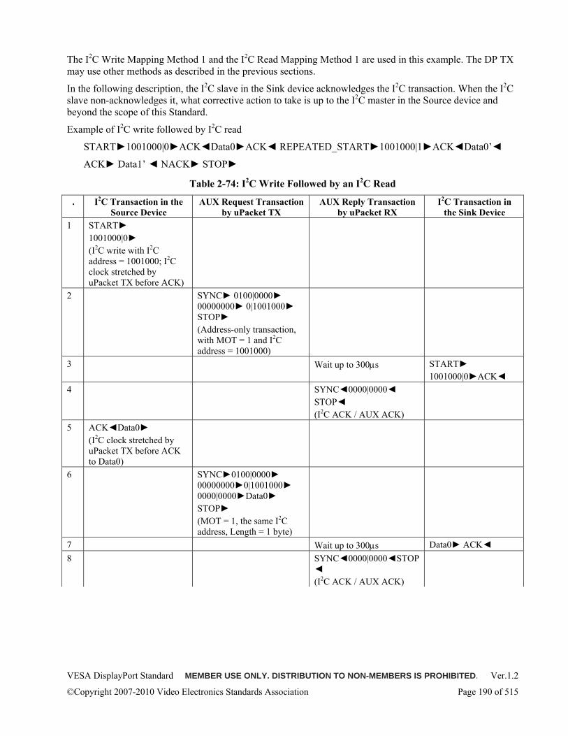
VESA DisplayPort Standard MEMBER USE ONLY. DISTRIBUTION TO NON-MEMBERS IS PROHIBITED. Ver.1.2
©Copyright 2007-2010 Video Electronics Standards Association Page 190 of 515
The I2C Write Mapping Method 1 and the I2C Read Mapping Method 1 are used in this example. The DP TX may use other methods as described in the previous sections.
In the following description, the I2C slave in the Sink device acknowledges the I2C transaction. When the I2C slave non-acknowledges it, what corrective action to take is up to the I2C master in the Source device and beyond the scope of this Standard.
Example of I2C write followed by I2C read
START1001000|0ACKData0ACK REPEATED_START1001000|1ACKData0’
ACK Data1’ NACK STOP
Table 2-74: I2C Write Followed by an I2C Read
. I2C Transaction in the Source Device
AUX Request Transaction by uPacket TX
AUX Reply Transaction by uPacket RX
I2C Transaction in the Sink Device
1 START 1001000|0 (I2C write with I2C address = 1001000; I2C clock stretched by uPacket TX before ACK)
2 SYNC 0100|0000 00000000 0|1001000 STOP (Address-only transaction, with MOT = 1 and I2C address = 1001000)
3 Wait up to 300μs START 1001000|0ACK
4 SYNC0000|0000 STOP (I2C ACK / AUX ACK)
5 ACKData0 (I2C clock stretched by uPacket TX before ACK to Data0)
6 SYNC0100|0000 000000000|1001000 0000|0000Data0 STOP (MOT = 1, the same I2C address, Length = 1 byte)
7 Wait up to 300μs Data0 ACK 8 SYNC0000|0000STOP
(I2C ACK / AUX ACK)
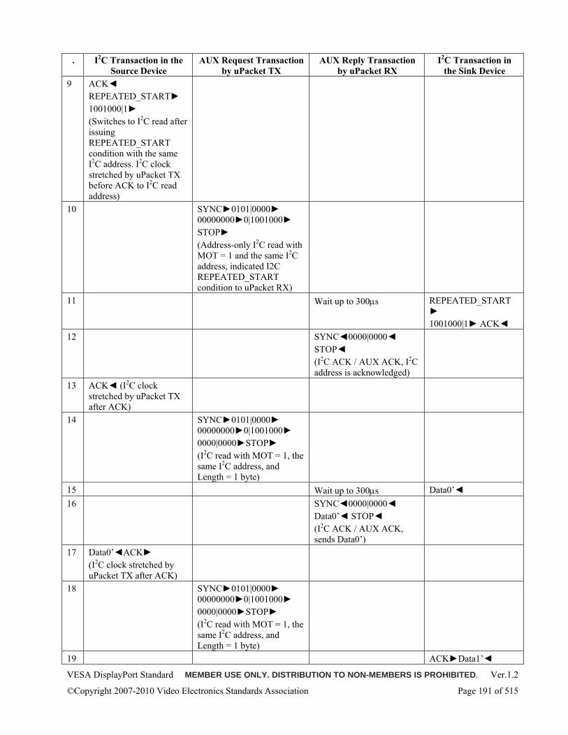
VESA DisplayPort Standard MEMBER USE ONLY. DISTRIBUTION TO NON-MEMBERS IS PROHIBITED. Ver.1.2
©Copyright 2007-2010 Video Electronics Standards Association Page 191 of 515
. I2C Transaction in the Source Device
AUX Request Transaction by uPacket TX
AUX Reply Transaction by uPacket RX
I2C Transaction in the Sink Device
9 ACK REPEATED_START 1001000|1 (Switches to I2C read after issuing REPEATED_START condition with the same I2C address. I2C clock stretched by uPacket TX before ACK to I2C read address)
10 SYNC0101|0000 000000000|1001000 STOP (Address-only I2C read with MOT = 1 and the same I2C address, indicated I2C REPEATED_START condition to uPacket RX)
11 Wait up to 300μs REPEATED_START 1001000|1 ACK
12 SYNC0000|0000 STOP (I2C ACK / AUX ACK, I2C address is acknowledged)
13 ACK (I2C clock stretched by uPacket TX after ACK)
14 SYNC0101|0000 000000000|1001000 0000|0000STOP (I2C read with MOT = 1, the same I2C address, and Length = 1 byte)
15 Wait up to 300μs Data0’ 16 SYNC0000|0000
Data0’ STOP (I2C ACK / AUX ACK, sends Data0’)
17 Data0’ACK (I2C clock stretched by uPacket TX after ACK)
18 SYNC0101|0000 000000000|1001000 0000|0000STOP (I2C read with MOT = 1, the same I2C address, and Length = 1 byte)
19 ACKData1’
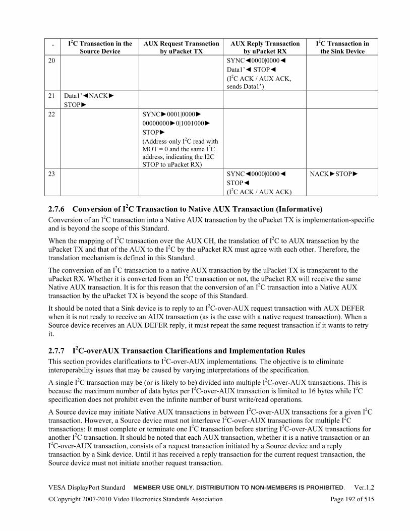
VESA DisplayPort Standard MEMBER USE ONLY. DISTRIBUTION TO NON-MEMBERS IS PROHIBITED. Ver.1.2
©Copyright 2007-2010 Video Electronics Standards Association Page 192 of 515
. I2C Transaction in the Source Device
AUX Request Transaction by uPacket TX
AUX Reply Transaction by uPacket RX
I2C Transaction in the Sink Device
20 SYNC0000|0000 Data1’ STOP (I2C ACK / AUX ACK, sends Data1’)
21 Data1’NACK STOP
22 SYNC0001|0000 000000000|1001000 STOP (Address-only I2C read with MOT = 0 and the same I2C address, indicating the I2C STOP to uPacket RX)
23 SYNC0000|0000 STOP (I2C ACK / AUX ACK)
NACKSTOP
2.7.6 Conversion of I2C Transaction to Native AUX Transaction (Informative) Conversion of an I2C transaction into a Native AUX transaction by the uPacket TX is implementation-specific and is beyond the scope of this Standard.
When the mapping of I2C transaction over the AUX CH, the translation of I2C to AUX transaction by the uPacket TX and that of the AUX to the I2C by the uPacket RX must agree with each other. Therefore, the translation mechanism is defined in this Standard.
The conversion of an I2C transaction to a native AUX transaction by the uPacket TX is transparent to the uPacket RX. Whether it is converted from an I2C transaction or not, the uPacket RX will receive the same Native AUX transaction. It is for this reason that the conversion of an I2C transaction into a Native AUX transaction by the uPacket TX is beyond the scope of this Standard.
It should be noted that a Sink device is to reply to an I2C-over-AUX request transaction with AUX DEFER when it is not ready to receive an AUX transaction (as is the case with a native request transaction). When a Source device receives an AUX DEFER reply, it must repeat the same request transaction if it wants to retry it.
2.7.7 I2C-overAUX Transaction Clarifications and Implementation Rules This section provides clarifications to I2C-over-AUX implementations. The objective is to eliminate interoperability issues that may be caused by varying interpretations of the specification.
A single I2C transaction may be (or is likely to be) divided into multiple I2C-over-AUX transactions. This is because the maximum number of data bytes per I2C-over-AUX transaction is limited to 16 bytes while I2C specification does not prohibit even the infinite number of burst write/read operations.
A Source device may initiate Native AUX transactions in between I2C-over-AUX transactions for a given I2C transaction. However, a Source device must not interleave I2C-over-AUX transactions for multiple I2C transactions: It must complete or terminate one I2C transaction before starting I2C-over-AUX transactions for another I2C transaction. It should be noted that each AUX transaction, whether it is a native transaction or an I2C-over-AUX transaction, consists of a request transaction initiated by a Source device and a reply transaction by a Sink device. Until it has received a reply transaction for the current request transaction, the Source device must not initiate another request transaction.
VESA DisplayPort Standard MEMBER USE ONLY. DISTRIBUTION TO NON-MEMBERS IS PROHIBITED. Ver.1.2
©Copyright 2007-2010 Video Electronics Standards Association Page 193 of 515
The syntax of the I2C transactions is very much implementation-dependent. The syntax specification does not assume any fixed I2C transaction syntax in an attempt to make it applicable to any I2C implementation. The I2C master of a uPacket RX in a Sink device will “imitate” the I2C_SCL/ I2C_DAT waveforms of those received by the I2C slave of a uPacket TX in a Source device (with the exception of the timing of I2C clock stretching as described in Section 2.7.7.1.6.8 and Section 2.7.7.2.6 of this document).
A uPacket TX in a Source device acting as an I2C slave and AUX Requester may not know how many data bytes its I2C master is intending to write or read in an I2C transaction. Unless it knows the number of data bytes at the beginning of an I2C transaction, the uPacket TX is recommended to generate I2C-over-AUX transactions with LEN value equal to 0 corresponding to one data byte. This way, the uPacket TX will not write or read more bytes than intended by its I2C master.
As far as the bit rate is concerned, the I2C specification lists certain bit rates (100k-/400k-/3.4M-bits/sec or bps) and the VESA E-DDC Standard (based on I2C as the PHY) notes the bit rate of 100kbps. In reality, however, the I2C bit rate is very dependent on implementations and “channel” qualities. Over a long-reach VGA cable, for example, it is common for a DDC master to have to reduce the bit rate down to 1k ~ 10kbps. The AUX CH bit rate, in comparison, is strictly required to be in the range of 1Mbps +/- 20% per Manchester format AUX transaction specification. The I2C-over-AUX specification comprehends this inherent difference (and the variation of the difference) of the bit rates between I2C and AUX CH. The extension of DPCD field for Sink device to declare its I2C bit rate capability and for Source device to set the I2C bit rate among those rates supported by the Sink device further adds to the robustness of the I2C-over-AUX specification for bridging the bit rate gap.
2.7.7.1 Clarifications for a Source Device This section describes the clarifications for a Source device.
2.7.7.1.1 Downstream I2C Bit Rate Detection/Configuration The extension to the DPCD field for a uPacket RX to declare its I2C bit rate capability and for a uPacket TX to set the I2C bit rate among those rates supported by the uPacket RX should be referenced. Alternatively, an uPacket TX and an uPacket RX may set the I2C bit rate in a vendor-specific manner.
At a low bit rate, the I2C slave interfacing with the I2C master within the uPacket RX takes a long time to accept/send bytes. At 1kbps, for example, the transport of one byte including ACK/NACK takes about 10ms. Therefore, the uPacket TX must extend the interval of successive I2C-over-AUX transactions in case the downstream I2C bit rate is low.
When an MST Source device is accessing the I2C slave of a DP device connected to via multiple MST Branch devices, the MST Source device must get the I2C bit rate of the DP device with the I2C slave and set the desired bit rate by originating REMOTE_ I2C _READ and REMOTE_ I2C _WRITE message transactions to the last MST Branch device driving the DP device. After setting the I2C bit rate, the MST Source device originates a REMOTE_ I2C message transaction to the last MST Branch device that generates the corresponding I2C-over-AUX transactions.
2.7.7.1.2 Prompting the Termination of I2C Transaction An address-only I2C-over-AUX (either write or read) with MOT bit set to 0 prompts the Sink device to issue I2C STOP condition to its I2C slave any time, even before the current I2C transaction is completed.
An address-only I2C-over-AUX with MOT bit set to 0 must not be issued when there is no on-going I2C-over-AUX transaction. If a Source device wants to initiate an I2C transaction to a certain I2C Device Address and then terminate it, the following I2C-over-AUX transactions must be used:
o Address-only transaction with MOT set to 1 o Address-only transaction with MOT set to 0
VESA DisplayPort Standard MEMBER USE ONLY. DISTRIBUTION TO NON-MEMBERS IS PROHIBITED. Ver.1.2
©Copyright 2007-2010 Video Electronics Standards Association Page 194 of 515
2.7.7.1.3 MOT Bit The MOT bit set to 0 prompts the Sink device to issue I2C STOP condition to its I2C slave after completing the current I2C-over-AUX transaction. As noted above, a Source device may issue an address-only I2C- over-AUX (either write or read) with MOT bit set to 0 any time to terminate the current I2C transaction even before its completion.
2.7.7.1.4 Prompting Repeatedd I2C Start Condition A Source device may issue I2C-over-AUX with MOT set to 1, then issue another I2C-over-AUX to the same I2C Device Address, but a different command (that is, write followed by read or read followed by write). This action by the Source device prompts the Sink device to initiate the second I2C transaction following Repeated I2C Start, instead of I2C STOP.
A Source device may also issue I2C-over-AUX with MOT set to 1, then issue another I2C-over-AUX to a different I2C Device Address either with the same command or a different command. This action also prompts the Sink device to initiate the second I2C transaction following Repeated Start condition, instead of I2C STOP condition.
2.7.7.1.5 I2C-write-over-AUX A Source device may start I2C-write-over-AUX request transaction either with:
- An address-only I2C-write-over-AUX with MOT bit set to 1, or
- Address+LEN+Data bytes I2C-write-over-AUX with MOT bit set to either 0 or 1
The remainder of this section describes the permissible I2C-over-AUX transactions following various replies from the Sink device. The Source device may issue a Native AUX transaction in between I2C-over-AUX transaction even before a given I2C transaction is completed/terminated.
2.7.7.1.5.1 Upon Receiving the Reply of I2C_ACK|AUX_ACK Followed by no “M” Value to a Request Transaction with MOT Bit Set to 0
The I2C transaction is completed. The Source device may initiate another AUX transaction, whether it is native AUX transaction or I2C-over-AUX transaction to either the same or different I2C Device Address.
2.7.7.1.5.2 Upon Receiving the Reply of I2C_ACK|AUX_ACK Followed by No “M” Value to a Request Transaction with MOT Bit Set to 1
The Source device must issue one of the following two I2C-over-AUX transactions
o Proceed with the next I2C-over-AUX transaction either with the same or different I2C Device Address. The transaction may be either I2C-write-over-AUX or I2C-read-over-AUX.
- If the ensuing I2C-over-AUX request transaction is either read or to a different I2C Device Address, the I2C master within the uPacket RX must issue a REPEATED START condition to its I2C Device Address
o Issue an address-only I2C-over-AUX with MOT bit set to 0 to prompt I2C STOP to terminate the current I2C-write-over-AUX transaction.
2.7.7.1.5.3 Upon I2C_DEFER|AUX_ACK Reply, with MOT Bit in Request Transaction Set to 0 or 1 The Source device must either:
o Issue I2C_WRITE_STATUS_UPDATE command, or
o Issue an address-only I2C-over-AUX with MOT bit set to 0 to prompt I2C STOP to terminate the current I2C-write-over-AUX transaction.
VESA DisplayPort Standard MEMBER USE ONLY. DISTRIBUTION TO NON-MEMBERS IS PROHIBITED. Ver.1.2
©Copyright 2007-2010 Video Electronics Standards Association Page 195 of 515
2.7.7.1.5.4 Upon the Reply of I2C_ACK|AUX_ACK Followed by “M” Value to the I2C-write-over-AUX, to a Request Transaction with MOT Bit Set to Either 0 or 1
The Source device must either:
o Issue I2C_WRITE_STATUS_UPDATE command, or
o Issue an address-only I2C-over-AUX with MOT bit set to 0 to prompt I2C STOP to terminate the current I2C-write-over-AUX transaction.
2.7.7.1.5.5 Upon Receiving I2C_NACK|AUX_ACK Reply Followed by Either “M” Value or no “M” Value, to a Request Transaction with MOT Bit Set Either to 0 or 1
After stopping the current I2C transaction by issuing Address-only I2C-over-AUX transaction with MOT set to 0, the Source device may start another AUX transaction. As one of the possible transactions, it may attempt the I2C-write-over-AUX transaction to the same I2C Device Address in order to make sure that the Sink device consistently I2C_NACKs
2.7.7.1.5.6 Upon Receiving AUX_DEFER Reply to a Request Transaction with MOT Bit Set to 0 or 1 The Source device must either:
o Repeat the identical I2C-write-over-AUX transaction keeping the same LEN value and Data bytes, or
o Issue an address-only I2C-over-AUX with MOT bit equal to 0 to prompt I2C STOP to terminate the current I2C-write-over-AUX transaction
2.7.7.1.5.7 Upon Receiving AUX_NACK Reply Followed by Either “M” Value or no “M” Value The Source device may initiate another AUX transaction. (A Sink device must not reply with AUX_NACK to I2C-write-over-AUX transaction unless there is a mismatch between the LEN+1 value and the number of received data bytes.)
2.7.7.1.5.8 No Reply The Source device may initiate another AUX transaction. (A Sink device must reply unless it either has detected an illegal command or is in a power-save mode due to the write of 02h value to DPCD Address 00600h by the Source device via a Native AUX transaction.)
2.7.7.1.6 I2C-read-over-AUX A Source device may start I2C-read-over-AUX request transaction either with:
- An address-only I2C-read-over-AUX with MOT set to 1, or
- An “Address+LEN” I2C-read-over-AUX with MOT set to either 0 or 1
The remainder of this section describes the permissible I2C-over-AUX transactions following various replies from the Sink device. The Source device may issue a native AUX transaction in between I2C-over-AUX transaction even before a given I2C transaction is completed/terminated.
2.7.7.1.6.1 Upon Receiving the Reply of I2C_ACK|AUX_ACK Followed by the “Total” Number of Data Bytes Equal to LEN+1, to a Request Transaction with MOT Set to 0
The I2C transaction is completed. The Source device may initiate another AUX transaction, whether it is native AUX transaction, I2C-over-AUX transaction to either the same or different I2C Device Address.
VESA DisplayPort Standard MEMBER USE ONLY. DISTRIBUTION TO NON-MEMBERS IS PROHIBITED. Ver.1.2
©Copyright 2007-2010 Video Electronics Standards Association Page 196 of 515
2.7.7.1.6.2 Upon Receiving the Reply of I2C_ACK|AUX_ACK Followed by the “Total” Number of Data Bytes Equal to LEN+1 to a Request Transaction with MOT Set to 1
The Source device must issue one of the following two I2C-over-AUX transactions
o Proceed with the next I2C-over-AUX transaction either with the same or different I2C Device Address. The transaction may be either I2C-write-over-AUX or I2C-read-over-AUX.
- If the ensuing I2C-over-AUX request transaction is either a write to any address or a read to a different I2C Device Address, the I2C master within the uPacket RX must issue a REPEATED START condition to its I2C Device Address
o Issue an address-only I2C-over-AUX with MOT bit set to 0 to prompt I2C STOP to terminate the current I2C-read-over-AUX transaction.
2.7.7.1.6.3 Upon I2C_DEFER|AUX_ACK Reply, to a Request Transaction with MOT Bit Set to 0 or 1 The Source device must either:
o Repeat the identical I2C-read-over-AUX transaction keeping the same LEN value, or
o Issue an address-only I2C-over-AUX with MOT bit set to 0 to prompt I2C STOP to terminate the current I2C-write-over-AUX transaction.
2.7.7.1.6.4 Upon the Reply of I2C_ACK|AUX_ACK Followed by the Total Number of Data Bytes Fewer than LEN+1, to a Request Transaction with MOT Bit Set Either to 0 or 1
The Source device must:
o Repeat the identical I2C-read-over-AUX transaction with the updated LEN value equal to the original LEN value minus the total number of data bytes received so far,
o Repeat the identical I2C-read-over-AUX transaction with the same LEN value as the original value, or,
o Issue an address-only I2C-over-AUX with MOT bit set to 0 to prompt I2C STOP to terminate the current I2C-read-over-AUX transaction.
It should be noted that when the Source device repeats the same I2C-read-over-AUX transaction with the same LEN value as the original value, the Sink device is likely to read more data bytes than the Source device needs.
2.7.7.1.6.5 Upon Receiving I2C_NACK|AUX_ACK Reply to a Request Transaction with MOT Bit Set to 0 or 1 For I2C read operation, I2C slave only asserts either ACK or NACK to the Device Address. For read data byte transfer from the slave to the master, it is the I2C master that asserts either ACK or NACK. Because of this fact, I2C_NACK|AUX_ACK reply to the I2C-read-over-AUX request transaction means that the I2C slave in the Sink device has asserted NACK to the specified I2C Device Address.
The Source device has the following options:
o Attempt an I2C-write-over-AUX to the same I2C Device Address in order to check whether the Sink device consistently I2C_NACK’s to that I2C Device Address
o Address-only I2C- over-AUX with MOT = 0 to prompt the Sink device to terminate the current I2C transaction
o Initiates an I2C- over-AUX to a different I2C Device Address prompting the Sink device to issue a Repeated I2C Start
2.7.7.1.6.6 Upon Receiving AUX_DEFER Reply to a Request Transaction with MOT Bit Set to 0 or 1
VESA DisplayPort Standard MEMBER USE ONLY. DISTRIBUTION TO NON-MEMBERS IS PROHIBITED. Ver.1.2
©Copyright 2007-2010 Video Electronics Standards Association Page 197 of 515
The Source device may:
o Repeat the identical I2C-read-over-AUX transaction keeping the same LEN value or
o Issue Address-only I2C-over-AUX with MOT bit set to 0 to prompt I2C STOP to terminate the current I2C-write-over-AUX transaction
2.7.7.1.6.7 No Reply The Source device may initiate another AUX transaction. (A Sink device must reply unless it either has detected an illegal command or is in a power-save mode due to the write of 02h value to DPCD Address 00600h by the Source device via a Native AUX transaction.)
2.7.7.1.6.8 Clock Stretching For an address-only I2C-over-AUX with MOT bit set to 1 and data byte transfer portion of I2C-write-over-AUX transaction, the I2C slave within a uPacket TX does not know in advance whether the uPacket RX will reply with I2C_ACK or I2C_NACK. Therefore, it must stretch the I2C clock after the 8th pulse (that is, the last data bit), instead of after the 9th pulse (that is, I2C ACK/NACK).
For data byte transfer portion of an I2C-read-over-AUX transaction, the I2C slave within a uPacket TX must stretch the I2C clock after the after the 9th pulse (that is, I2C ACK/NACK) to monitor whether its I2C master will assert I2C ACK or NACK to the data byte.
2.7.7.2 Clarifications for a Sink Device This section describes the clarifications for a Sink device.
2.7.7.2.1 I2C Bit Rate Capability Declaration and Setting A device with uPacket RX such as a Sink device declares its I2C it rate capability at I2C_SPEED_CONTROL_CAPABILITY field at DPCD Address 0000Ch. A device with uPacket TX such as a Source device sets the I2C bit rate by writing to I2C_SPEED_CONTROL_SELECT field at DPCD Address 00109h. Alternatively, uPacket TX and uPacket RX may set the I2C bit rate in a vendor-specific manner.
2.7.7.2.2 Termination/Completion of I2C Transaction Upon receiving an address-only I2C-over-AUX request transaction with MOT bit set to 0 from a Source device, the Sink device must issue I2C STOP condition to its I2C slave promptly, even before the current I2C transaction is completed.
Upon receiving an address+LEN+Data bytes (for write, no Data bytes for read) I2C-over-AUX request transaction with MOT set to 0 from a Source device, the Sink device must issue I2C STOP condition upon completion of the current I2C-over-AUX transaction; that is, when all the address and/or data bytes have been ACKed by its I2C slave.
When a Source device initiates a new I2C transaction without properly completing/terminating the current I2C transaction (which a Source device must not do), a Sink device is recommended to reply with an I2C_NACK|AUX_ACK and issue I2C STOP condition to its I2C slave.
When a Source device neither completes/terminates nor initiates a new I2C transaction, a Sink device must time-out after a certain period (for example, 1 sec) and issue I2C STOP condition to its I2C slave in order to avoid locking up the I2C bus within a Sink device indefinitely. This scenario is possible when a Source device is powered down, disconnected, or somehow locked up in the middle of an I2C transaction.
A Sink device supporting detection of Source and/or Powered-Source is recommended to issue I2C STOP condition to its I2C slave when a disconnect event is detected in the middle of an I2C transaction.
2.7.7.2.3 REPEATED I2C START Condition
VESA DisplayPort Standard MEMBER USE ONLY. DISTRIBUTION TO NON-MEMBERS IS PROHIBITED. Ver.1.2
©Copyright 2007-2010 Video Electronics Standards Association Page 198 of 515
A Source device may issue I2C-over-AUX with MOT set to 1, then issue another I2C-over-AUX to the same I2C Device Address, but a different command (that is, write followed by read or read followed by write).
A Source device may also issue I2C-over-AUX with MOT set to 1, then issue another I2C-over-AUX to a different I2C Device Address with the same command (that is, write followed by write or read followed by read).
The Sink device must initiate the second I2C transaction following Repeated I2C Start, instead of I2C STOP.
2.7.7.2.4 I2C-write-over-AUX This section describes the permissible replies by a Sink device after receiving an I2C-write-over-AUX request transaction from a Source device. A Sink device must reply with one of the ways as described in this section.
2.7.7.2.4.1 I2C_ACK|AUX_ACK Followed by No “M” Value - All the data bytes have been written to and ACKed by the I2C slave.
o When the MOT bit was 0, the I2C transaction is complete. The Sink device must issue I2C STOP condition to its I2C slave.
o When the MOT bit was 1, the I2C transaction is still ongoing. The Sink device must not issue I2C STOP condition.
If the ensuing I2C-over-AUX transaction is either I2C-read-over-AUX or to a different I2C Device Address, the Sink device must issue I2C REPEATED START condition to its I2C slave.
2.7.7.2.4.2 I2C_ACK|AUX_ACK Followed by “M” Value Of the data bytes sent by the Source device, the number of bytes equal to M (that is smaller than LEN+1 value) have been written to and ACK’ed by the I2C slave
The Sink device must continue writing to its I2C slave until the number of bytes equal to LEN+1 has been ACKed by the slave.
o Upon receiving ensuing I2C_WRITE_STATUS_UPDATE request transaction, the Sink device must reply with I2C_ACK|AUX_ACK with the updated “M” value.
o Upon receiving ensuing address-only I2C-over-AUX with MOT bit set to 0 transaction, the Sink device must issue I2C STOP condition to its slave promptly even before the completion of the current I2C transaction.
o Upon receiving ensuing I2C-over-AUX transaction that is neither I2C_WRITE_STATUS_UPDATE nor an address-only I2C-over-AUX with MOT bit set to 0, the Sink device is recommended to reply with I2C_NACK|AUX_ACK to the Source device and issue I2C STOP condition to its slave promptly even before the completion of the current I2C transaction. (A Source device must issue either I2C _WRITE_STATUS_UPDATE or an address-only- I2C-over-AUX with MOT bit set to 0.)
2.7.7.2.4.3 I2C_DEFER|AUX_ACK None of the data bytes has been ACKed/NACKed by the I2C slave
o A Sink device must continue writing to its I2C slave until the number of bytes equal to LEN+1 has been ACK’ed by the slave.
Upon receiving ensuing I2C_WRITE_STATUS_UPDATE request transaction, the Sink device must reply with I2C_ACK|AUX_ACK with the updated “M” value. If the Sink
VESA DisplayPort Standard MEMBER USE ONLY. DISTRIBUTION TO NON-MEMBERS IS PROHIBITED. Ver.1.2
©Copyright 2007-2010 Video Electronics Standards Association Page 199 of 515
device has yet to receive ACK from the I2C slave, however, it is to issue I2C_DEFER|AUX_ACK again
Upon receiving ensuing address-only I2C-over-AUX with MOT bit set to 0 transaction, the Sink device must reply with I2C_ACK|AUX_ACK to the Source device and issue I2C STOP condition to its slave promptly even before the completion of the current I2C transaction.
Upon receiving ensuing I2C-over-AUX transaction that is neither I2C_WRITE_STATUS_UPDATE nor an address-only I2C-over-AUX with MOT bit set to 0, the Sink device is recommended to reply with I2C_NACK|AUX_ACK to the Source device and issue I2C STOP condition to its slave promptly even before the completion of the current I2C transaction. (A Source device must issue either I2C_WRITE_STATUS_UPDATE or an address-only- I2C-over-AUX with MOT bit set to 0.)
2.7.7.2.4.4 I2C_NACK|AUX_ACK Followed by Either “M” Value or No “M” Value Either I2C Device Address or Data byte are NACKed by the I2C slave
2.7.7.2.4.5 AUX_DEFER A Sink device is handling the request, but is not ready to reply with either I2C_ACK or I2C_NACK. Until NACKed by the I2C slave, the Sink device must continue handling the request.
o Upon receiving ensuing I2C-write-over-AUX transaction identical to the previous one (the same I2C Device Address, LEN value, and Data bytes), the Sink device will reply to the Source device as described in this section while continuing handling the request.
o Upon receiving ensuing address-only I2C-write -AUX with MOT bit set to 0 transaction, the Sink device must reply with I2C_ACK|AUX_ACK to the Source device and issue I2C STOP condition to its slave promptly even before the completion of the current I2C transaction.
o Upon receiving ensuing I2C-over-AUX transaction that is neither identical to the previous one nor an address only I2C-write-over-AUX transaction, the Sink device is recommended to reply with I2C_NACK|AUX_ACK to the Source device and issue I2C STOP condition to its slave promptly even before the completion of the current I2C transaction. (A Source device must issue either an I2C-write-over-AUX transaction identical to the previous one or an address-only- I2C-over-AUX with MOT bit set to 0.)
2.7.7.2.4.6 AUX_NACK Followed by Either “M” Value or No “M” Value A Sink device must not reply with AUX_NACK to I2C-write-over-AUX transaction unless there is a mismatch between the LEN+1 value and the number of received data bytes.
2.7.7.2.4.7 No Reply A Sink device must reply unless it either has detected an illegal command or is in a power-save mode due to the write of 02h value to DPCD Address 00600h by the Source device via a Native AUX transaction.
2.7.7.2.5 I2C -read-over-AUX This section describes the permissible replies by a Sink device after receiving an I2C-read-over-AUX request transaction from a Source device. A Sink device must reply with one of the ways as shown in this section.
2.7.7.2.5.1 I2C_ACK|AUX_ACK Followed by the Total Number of Data Bytes Equal to LEN+1 All the data bytes have been read from the I2C slave.
VESA DisplayPort Standard MEMBER USE ONLY. DISTRIBUTION TO NON-MEMBERS IS PROHIBITED. Ver.1.2
©Copyright 2007-2010 Video Electronics Standards Association Page 200 of 515
o When the MOT bit was 0, the I2C transaction is complete. The Sink device must issue NACK to the final Data byte and issue I2C STOP condition to its I2C slave.
o When the MOT bit was 1, the I2C transaction is still on-going. The Sink device must not issue I2C STOP condition.
If the ensuing I2C-over-AUX transaction is I2C-write-over-AUX or I2C-read-over-AUX to a different I2C Device Address, the Sink device must issue REPEATED I2C START condition to its I2C slave.
2.7.7.2.5.2 I2C_ACK|AUX_ACK Followed by the Total Number of Bytes Fewer than LEN+1 The Sink device must continue reading from its I2C slave until the number of bytes equal to LEN+1 has been read.
Upon receiving ensuing I2C-read-over-AUX transaction to the same I2C Device with the LEN value updated to equal to the original value minus the total number of bytes replied by the Sink device so far, the Sink device must reply with I2C_ACK|AUX_ACK with the Data bytes that have been read from the Slave but were not replied back to the Source device in the previous reply transaction(s).
Upon receiving ensuing I2C-read-over-AUX transaction to the same I2C Device with the same LEN value as the original value, the Sink device must reply with number of data bytes equal to LEN value + 1 (or fewer if it cannot) irrespective of how many bytes it had already replied.
Upon receiving ensuing Address-only I2C-over-AUX transaction with MOT = 0, the Sink device must terminate the I2C transaction by issuing I2C STOP.
Upon receiving ensuing I2C-over-AUX transaction that is none of the above, the Sink device is recommended to reply with I2C_NACK|AUX_ACK to the Source device and issue I2C STOP condition to its slave promptly even before the completion of the current I2C transaction.
2.7.7.2.5.3 I2C_DEFER|AUX_ACK A Sink device must continue reading from its I2C slave until the number of bytes equal to LEN+1 has been read.
Upon receiving ensuing I2C-read-over-AUX transaction identical to the previous one (the same I2C Device Address and LEN value), the Sink device must reply with I2C_ACK|AUX_ACK with the Data bytes that have been read from the Slave but were not replied back to the Source device in the previous reply transaction.
Upon receiving ensuing address-only I2C-over-AUX with MOT bit set to 0 transaction, the Sink device must reply with I2C_ACK|AUX_ACK to the Source device and issue I2C STOP condition to its slave promptly even before the completion of the current I2C transaction.
Upon receiving ensuing I2C-over-AUX transaction that is neither identical to the previous one nor an address-only I2C-over-AUX with MOT bit set to 0, the Sink device is recommended to reply with I2C_NACK|AUX_ACK to the Source device and issue I2C STOP condition to its slave promptly even before the completion of the current I2C transaction.
2.7.7.2.5.4 I2C_NACK|AUX_ACK I2C Device Address is NACKed by the I2C slave.
VESA DisplayPort Standard MEMBER USE ONLY. DISTRIBUTION TO NON-MEMBERS IS PROHIBITED. Ver.1.2
©Copyright 2007-2010 Video Electronics Standards Association Page 201 of 515
It should be noted that the Sink device is not to terminate the I2C transaction following I2C_NACK to the I2C Device Address. Therefore, the Source device must prompt the termination by issuing an address-only I2C-over-AUX transaction with MOT bit set to 0.
2.7.7.2.5.5 AUX_DEFER The Sink device is handling the request, but is not ready to reply with either I2C_ACK or I2C_NACK. Until NACKed by the I2C slave (to the I2C Device Address). The Sink device must continue handling the request.
o Upon receiving ensuing I2C-read-over-AUX transaction identical to the previous one (the same I2C Device Address and LEN value), the Sink device will reply to the Source device as described in this section while continuing handling the request.
o Upon receiving ensuing address-only I2C-over-AUX transaction with MOT bit set to 0, the Sink device must reply with I2C_ACK|AUX_ACK to the Source device and issue I2C STOP condition to its slave promptly even before the completion of the current I2C transaction.
o Upon receiving ensuing I2C-over-AUX transaction that is neither identical to the previous one nor an address only I2C-read-over-AUX transaction, the Sink device is recommended to reply with I2C_NACK|AUX_ACK to the Source device and issue I2C STOP condition to its slave promptly even before the completion of the current I2C transaction.
2.7.7.2.5.6 AUX_NACK A Sink device must not reply with AUX_NACK to I2C-read-over-AUX transaction.
2.7.7.2.5.7 No Reply A Sink device must reply unless it either has detected an illegal command or is in a power-save mode due to the write of 02h value to DPCD Address 00600h by the Source device via a Native AUX transaction.
2.7.7.2.6 Clock Stretching When reading the last data byte of an I2C-read-over-AUX with MOT bit set to 1, I2C master within a uPacket RX must stretch the I2C clock after the 8th pulse (that is, the last data bit), instead of after the 9th pulse (I2C ACK/NACK). When the ensuing I2C-over-AUX transaction is the address-only with MOT bit set to 0, the I2C master within the uPacket RX must assert I2C NACK to its I2C slave. Otherwise, it must assert I2C ACK.
For I2C Device Address and data write, I2C master within a uPacket RX must stretch the I2C clock after the 9th pulse (that is, ACK/NACK bit).
VESA DisplayPort Standard MEMBER USE ONLY. DISTRIBUTION TO NON-MEMBERS IS PROHIBITED. Ver.1.2
©Copyright 2007-2010 Video Electronics Standards Association Page 202 of 515
2.8 Transaction Syntax in FAUX Transaction Format This section describes FAUX transaction syntaxes for Native AUX and I2C-over-AUX transactions. As described in Section 3.4, the FAUX transaction format uses ANSI8B/10B coding with an effective bit rate of 576Mbps.
The transaction syntax is preceded by FAUX Preamble and FAUX Start symbol, and is followed by FAUX End symbol as described in Section 3.4.1.5.
The syntaxes for Native AUX and I2C-over-AUX transactions in FAUX mode are the same as those in Manchester mode as described in Section 2.7 except for the following differences:
o CRC16 is inserted by the transmitting end, which is uPacket TX for a Request transaction and uPacket RX for Reply transaction.
o When CRC16 error is detected in the Request transaction, the uPacket RX must reply with AUX_NACK.
o When CRC16 error is detected in the Reply transaction, the uPacket TX must ignore the reply. o Maximum burst data size is increased to 64 bytes: LEN field is extended from 4 bits to 6 bits, with the
LEN value of 3Fh corresponding to the burst data size of 64 bytes. The response time-out period for the Replier (uPacket RX) and the reply time-out period for the Requester (uPacket TX) are 0.5us and 1.0us, respectively, in FAUX mode.
VESA DisplayPort Standard MEMBER USE ONLY. DISTRIBUTION TO NON-MEMBERS IS PROHIBITED. Ver.1.2
©Copyright 2007-2010 Video Electronics Standards Association Page 203 of 515
2.9 AUX CH Services This section describes two types of AUX CH services, AUX CH Link Services and AUX CH Device Services. These are the Link Layer services used by “Policy Makers” for link and device management both in the Source device and the Sink device.
Whenever the Hot Plug Detect signal is active (the connectors are plugged in and the Sink device has at least a “trickle” AC power), AUX CH services must be available.
There are two Policy Makers.
• Stream Policy Maker
o Manages stream
Stream transport initialization, and maintenance (More on this subject is covered in the following sections)
Uses AUX CH Device Services
Gets link information from Link Policy Maker
• Link Policy Maker
o Manages link
Link discovery, initialization, and maintenance
Uses AUX CH Link Services
Both Source and Sink devices must have these two policy makers. Policy Makers may be implemented as operating system, software driver, firmware, or hardware state machine. The choice is implementation-specific.
In this document, only the semantics of the interface between the Link Layer and Stream Policy Makers is defined: Syntax (i.e., API) is implementation-specific, and not covered in the DisplayPort Standard.
2.9.1 Stream Transport Initiation Sequence The Stream Source Policy Maker, before transport initiation, must take the following actions:
• Read EDID from the Sink device
• Set stream attributes for Main Stream attribute data and CEA 861-C InfoFrame generation
• Optionally (recommended), get the following information from the Link Policy Maker
o Link configuration: Total link bandwidth
To avoid oversubscription of the link bandwidth
o RX capability: Number and types of ports available in RX
To determine the number and types of streams that may be transported
o Link status: Synchronized? Excessive error symbols?
To make sure that the link is ready for transport
When a stream is ready for transport, the Stream Source Policy Maker must start the transport of isochronous stream along with stream attributes data.
The Stream sink, upon receiving a stable stream, must decode the stream attributes data and start reconstructing the incoming isochronous stream.
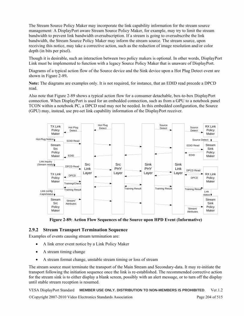
VESA DisplayPort Standard MEMBER USE ONLY. DISTRIBUTION TO NON-MEMBERS IS PROHIBITED. Ver.1.2
©Copyright 2007-2010 Video Electronics Standards Association Page 204 of 515
The Stream Source Policy Maker may incorporate the link capability information for the stream source management: A DisplayPort aware Stream Source Policy Maker, for example, may try to limit the stream bandwidth to prevent link bandwidth oversubscription. If a stream is going to oversubscribe the link bandwidth, the Stream Source Policy Maker may inform the stream source. The stream source, upon receiving this notice, may take a corrective action, such as the reduction of image resolution and/or color depth (in bits per pixel).
Though it is desirable, such an interaction between two policy makers is optional. In other words, DisplayPort Link must be implemented to function with a legacy Source Policy Maker that is unaware of DisplayPort.
Diagrams of a typical action flow of the Source device and the Sink device upon a Hot Plug Detect event are shown in Figure 2-89.
Note: The diagrams are examples only. It is not required, for instance, that an EDID read precede a DPCD read.
Also note that Figure 2-89 shows a typical action flow for a consumer detachable, box-to-box DisplayPort connection. When DisplayPort is used for an embedded connection, such as from a GPU to a notebook panel TCON within a notebook PC, a DPCD read may not be needed. In this embedded configuration, the Source (GPU) may, instead, use pre-set link capability information of the DisplayPort receiver.
StreamSrc
Policy Maker
Sink PHY Layer
SinkLink
Layer
Stream Sink
Policy MakerEDIDEDID
Training Result
SourceDetect
EDID Read
SourceDetect
DPCD Read
DPCD
Training Result
RX Link Policy Maker
SrcPHY Layer
SrcLink
Layer
EDID Read
DPCD Read
Training/Check
TX Link Policy Maker
Hot Plug DetectHot Plug
DetectRX Link Policy Maker
TX Link Policy Maker
DPCD
Training Result
Stream Src
Policy Maker
Stream/Attributes
Training Result
StreamSink
Policy MakerStream/
Attributes
Hot-Plug Notice
Link inquiry(Stream ready)
Link config/caps/status
Source Detect
Link status
Figure 2-89: Action Flow Sequences of the Source upon HPD Event (Informative)
2.9.2 Stream Transport Termination Sequence Examples of events causing stream termination are:
• A link error event notice by a Link Policy Maker
• A stream timing change
• A stream format change, unstable stream timing or loss of stream
The stream source must terminate the transport of the Main Stream and Secondary-data. It may re-initiate the transport following the initiation sequence once the link is re-established. The recommended corrective action for the stream sink is to either display a blank screen, possibly with an alert message, or to turn off the display until stable stream reception is resumed.
VESA DisplayPort Standard MEMBER USE ONLY. DISTRIBUTION TO NON-MEMBERS IS PROHIBITED. Ver.1.2
©Copyright 2007-2010 Video Electronics Standards Association Page 205 of 515
2.9.3 AUX Link Services In order to transport isochronous data stream from the Source device to the Sink device, the Link Policy Maker must first establish the Main Link. The Main Link must be established in the following sequence of steps.
Note: All the commands are memory mapped, whether setting or getting link parameters.
Step_1:
Unless it has pre-set knowledge, the Source must initiate Link Discovery, by reading the Link Capability field of the DPCD through the AUX CH. The Link Capability field must describe the link capability of the DisplayPort receiver in the Sink device, such as the Main Link maximum bit rate and maximum number of lanes. Details on reading the DPCD are explained later in this section.
Step_2:
Based on the DPCD information, the Source must start the Link Initialization process. The following sequences must take place during Link Initialization:
• The Link Policy Maker in the Source device must start Link Training. This function call notifies the Sink of the ensuing transport of the training pattern through the Main Link PHY layer, with link configuration and training attributes defined in this function.
• The Link Policy Maker of the Source device must check the training status and report of final results to the Stream Policy Maker.
If the Link Policy Maker detects a failed Link Training attempt, it must take corrective action. Possible correction actions are:
• Reduction of the bit rate if the link was in the high bit rate mode,
• Termination of Link Initialization
This loop of setting the Main Link configuration and forwarding training pattern, while checking the status must end with the final result of either pass or fail. “Pass” means that the bit lock and symbol lock have been achieved on each of the configured lanes, and all the lanes are symbol locked with proper inter-lane alignment (with skew of two LS_Clk period between adjacent lanes). Otherwise, it is “fail”.
After the Main Link is established, the Link Policy Maker of the Source device must check the link status whenever it detects the HPD (Hot Plug Detect) signal toggle after the rising edge of HPD. The Source device must ignore low or high pulse period of less than 0.25ms. In other words, the Source device must not check the link status until at least 0.25ms after the rising edge.
The Sink device must clear the HPD signal to a low level for 0.5ms to 1ms before setting it high again whenever there is a status change either in the link or in the device. This will notify the Source device of the status change.
The Source device must check the Link Status field of the DPCD through an AUX CH read transaction to identify the cause within 100ms of the rising edge of the HPD. Upon identifying the cause, the Link Policy Maker must take corrective action.
Note (Informative): In case the HPD signal toggling (or bouncing) is the result of the Hot Unplug followed by Hot Plug of a cable-connector assembly, then the HPD signal is likely to remain unstable during the debouncing period, which is in the order of tens of ms. The Source device may either check the stability of the HPD signal before initiating an AUX CH read transaction or immediately initiate the AUX CH read transaction after each HPD rising edge.
VESA DisplayPort Standard MEMBER USE ONLY. DISTRIBUTION TO NON-MEMBERS IS PROHIBITED. Ver.1.2
©Copyright 2007-2010 Video Electronics Standards Association Page 206 of 515
2.9.3.1 Address Mapping for Link Configuration/Management Table 2-75 shows the DisplayPort address mapping for DPCD. The DPCD is byte addressed.
Table 2-75: Address Mapping for DPCD (DisplayPort Configuration Data)
DisplayPort Address
Definition Read/Write over AUX CH
Receiver Capability Field
00000h DPCD_REV : DPCD revision number Bits 3:0 = Minor revision number Bits 7:4 = Major revision number
10h for DPCD Rev.1.0 11h for DPCD Rev.1.1 12h for DPCD Rev 1.2 A DP device with uPacket RX with a DPCD Revision number of 1.2 and above must support GUID at DPCD Addresses 00030h ~ 0003Fh. Furthermore, a DP Sink device with DPCD Rev.1.2 with a stereo display capability support (as declared in EDID and Display ID) must support the handling of 3D Stereo in-band signaling using Video_Stream_Configuration (VSC) Packet.
Note: The DPCD revision number does not necessarily match the DisplayPort version number.
Read Only
00001h MAX_LINK_RATE : Maximum link rate of Main Link lanes = Value x 0.27Gbps per lane Bits 7:0 = MAX_LINK_RATE
For DisplayPort Ver.1.1, only two values are supported. All other values are RESERVED.
06h = 1.62Gbps per lane 0Ah = 2.7Gbps per lane 14h = 5.4Gbps per lane
A uPacket RX of an MST Branch device must return its own capability. A uPacket RX of an SST Branch device must return the lowest common denominator of its own value and the Downstream link value.
Read Only
VESA DisplayPort Standard MEMBER USE ONLY. DISTRIBUTION TO NON-MEMBERS IS PROHIBITED. Ver.1.2
©Copyright 2007-2010 Video Electronics Standards Association Page 207 of 515
DisplayPort Address
Definition Read/Write over AUX CH
00002h MAX_LANE_COUNT : Maximum number of lanes = Value Bits 4:0 = MAX_LANE_COUNT
For Rev.1.1, only the following three values are supported. All other values are RESERVED.
1h = 1-lane 2h = 2-lanes 4h = 4-lanes
For 1-lane configuration, Lane 0 is used. For 2-lane configuration, Lane 0 and Lane 1 are used. A Branch device must return the lowest common denominator of its own value and the Downstream link value of Bits 4:0. For DPCD Rev.1.0
Bits 7:5 = RESERVED. Read all 0s. For DPCD Rev.1.1
Bits 6:5 = RESERVED. Read all 0s. Bit 7 = ENHANCED_FRAME_CAP (Applies only to Single Stream Format)
0 = Enhanced Framing symbol sequence for BS, SR, CPBS, and CPSR is not supported. 1 = Enhanced Framing symbol sequence for BS, SR, CPBS, and CPSR is supported as described in Section 2.2.1.2 A uPacket RX with DPCD Revision number (as expressed at DPCD 00000h) 1.2 or higher must set this bit to 1.
For DPCD Rev.1.2 Bit 5 = RESERVED. Read 0 Bit 6 = TPS3_SUPPORTED
0 = TPS3 (Training pattern sequence 3) is not supported 1 = TPS3 (Training pattern sequence 3) is supported (mandatory for Downstream devices that support HBR2, optional for others)
Read Only
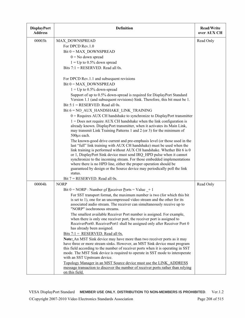
VESA DisplayPort Standard MEMBER USE ONLY. DISTRIBUTION TO NON-MEMBERS IS PROHIBITED. Ver.1.2
©Copyright 2007-2010 Video Electronics Standards Association Page 208 of 515
DisplayPort Address
Definition Read/Write over AUX CH
00003h MAX_DOWNSPREAD For DPCD Rev.1.0
Bit 0 = MAX_DOWNSPREAD 0 = No down spread
1 = Up to 0.5% down spread Bits 7:1 = RESERVED. Read all 0s.
For DPCD Rev.1.1 and subsequent revisions
Bit 0 = MAX_DOWNSPREAD 1 = Up to 0.5% down-spread Support of up to 0.5% down-spread is required for DisplayPort Standard Version 1.1 (and subsequent revisions) Sink. Therefore, this bit must be 1.
Bit 5:1 = RESERVED. Read all 0s. Bit 6 = NO_AUX_HANDSHAKE_LINK_TRAINING
0 = Requires AUX CH handshake to synchronize to DisplayPort transmitter 1 = Does not require AUX CH handshake when the link configuration is already known. DisplayPort transmitter, when it activates its Main Link, may transmit Link Training Patterns 1 and 2 (or 3) for the minimum of 500μs each. The known-good drive current and pre-emphasis level (or those used in the last “full” link training with AUX CH handshake) must be used when the link training is performed without AUX CH handshake. Whether Bit 6 is 0 or 1, DisplayPort Sink device must send IRQ_HPD pulse when it cannot synchronize to the incoming stream. For those embedded implementations where there is no HPD line, either the proper operation should be guaranteed by design or the Source device may periodically poll the link status.
Bit 7 = RESERVED. Read all 0s.
Read Only
00004h NORP Bit 0 = NORP : Number of Receiver Ports = Value _+ 1
For SST transport format, the maximum number is two (for which this bit is set to 1), one for an uncompressed video stream and the other for its associated audio stream. The receiver can simultaneously receive up to "NORP" isochronous streams. The smallest available Receiver Port number is assigned. For example, when there is only one receiver port, the receiver port is assigned to ReceiverPort0. ReceiverPort1 shall be assigned only after Receiver Port 0 has already been assigned.
Bits 7:1 = RESERVED. Read all 0s. Note: An MST Sink device may have more than two receiver ports as it may have three or more stream sinks. However, an MST Sink device must program this field according to the number of receiver ports when it is operating in SST mode. The MST Sink device is required to operate in SST mode to interoperate with an SST Upstream device. Topology Manager in an MST Source device must use the LINK_ADDRESS message transaction to discover the number of receiver ports rather than relying on this field.
Read Only
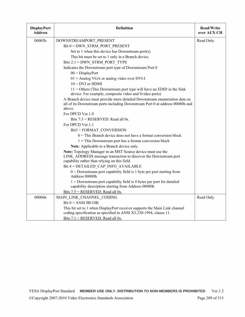
VESA DisplayPort Standard MEMBER USE ONLY. DISTRIBUTION TO NON-MEMBERS IS PROHIBITED. Ver.1.2
©Copyright 2007-2010 Video Electronics Standards Association Page 209 of 515
DisplayPort Address
Definition Read/Write over AUX CH
00005h DOWNSTREAMPORT_PRESENT Bit 0 = DWN_STRM_PORT_PRESENT
Set to 1 when this device has Downstream port(s) This bit must be set to 1 only in a Branch device.
Bits 2:1 = DWN_STRM_PORT_TYPE Indicates the Downstream port type of Downstream Port 0
00 = DisplayPort 01 = Analog VGA or analog video over DVI-I 10 = DVI or HDMI 11 = Others (This Downstream port type will have no EDID in the Sink device: For example, composite video and Svideo ports)
A Branch device must provide more detailed Downstream enumeration data on all of its Downstream ports including Downstream Port 0 at address 00080h and above. For DPCD Ver.1.0
Bits 7:3 = RESERVED. Read all 0s. For DPCD Ver.1.1
Bit3 = FORMAT_CONVERSION 0 = This Branch device does not have a format conversion block 1 = This Downstream port has a format conversion block
Note: Applicable to a Branch device only. Note: Topology Manager in an MST Source device must use the LINK_ADDRESS message transaction to discover the Downstream port capability rather than relying on this field. Bit 4 = DETAILED_CAP_INFO_AVAILABLE
0 = Downstream port capability field is 1 byte per port starting from Address 00080h 1 = Downstream port capability field is 4 bytes per port for detailed capability description starting from Address 00080h
Bits 7:5 = RESERVED. Read all 0s.
Read Only
00006h MAIN_LINK_CHANNEL_CODING Bit 0 = ANSI 8B/10B This bit set to 1 when DisplayPort receiver supports the Main Link channel coding specification as specified in ANSI X3.230-1994, clause 11. Bits 7:1 = RESERVED. Read all 0s.
Read Only
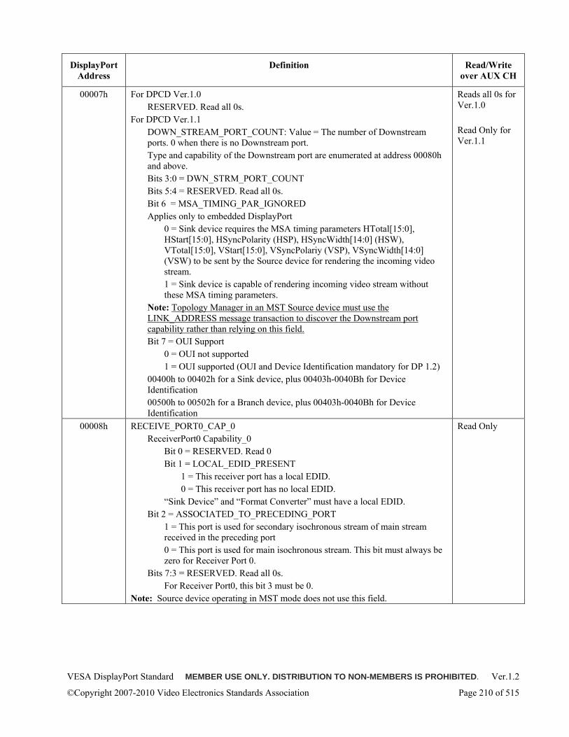
VESA DisplayPort Standard MEMBER USE ONLY. DISTRIBUTION TO NON-MEMBERS IS PROHIBITED. Ver.1.2
©Copyright 2007-2010 Video Electronics Standards Association Page 210 of 515
DisplayPort Address
Definition Read/Write over AUX CH
00007h For DPCD Ver.1.0 RESERVED. Read all 0s.
For DPCD Ver.1.1 DOWN_STREAM_PORT_COUNT: Value = The number of Downstream ports. 0 when there is no Downstream port. Type and capability of the Downstream port are enumerated at address 00080h and above. Bits 3:0 = DWN_STRM_PORT_COUNT Bits 5:4 = RESERVED. Read all 0s. Bit 6 = MSA_TIMING_PAR_IGNORED Applies only to embedded DisplayPort
0 = Sink device requires the MSA timing parameters HTotal[15:0], HStart[15:0], HSyncPolarity (HSP), HSyncWidth[14:0] (HSW), VTotal[15:0], VStart[15:0], VSyncPolariy (VSP), VSyncWidth[14:0] (VSW) to be sent by the Source device for rendering the incoming video stream. 1 = Sink device is capable of rendering incoming video stream without these MSA timing parameters.
Note: Topology Manager in an MST Source device must use the LINK_ADDRESS message transaction to discover the Downstream port capability rather than relying on this field. Bit 7 = OUI Support
0 = OUI not supported 1 = OUI supported (OUI and Device Identification mandatory for DP 1.2)
00400h to 00402h for a Sink device, plus 00403h-0040Bh for Device Identification 00500h to 00502h for a Branch device, plus 00403h-0040Bh for Device Identification
Reads all 0s for Ver.1.0 Read Only for Ver.1.1
00008h RECEIVE_PORT0_CAP_0 ReceiverPort0 Capability_0
Bit 0 = RESERVED. Read 0 Bit 1 = LOCAL_EDID_PRESENT
1 = This receiver port has a local EDID. 0 = This receiver port has no local EDID.
“Sink Device” and “Format Converter” must have a local EDID. Bit 2 = ASSOCIATED_TO_PRECEDING_PORT
1 = This port is used for secondary isochronous stream of main stream received in the preceding port 0 = This port is used for main isochronous stream. This bit must always be zero for Receiver Port 0.
Bits 7:3 = RESERVED. Read all 0s. For Receiver Port0, this bit 3 must be 0.
Note: Source device operating in MST mode does not use this field.
Read Only
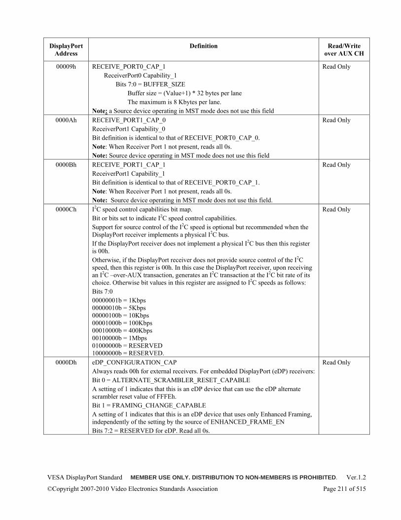
VESA DisplayPort Standard MEMBER USE ONLY. DISTRIBUTION TO NON-MEMBERS IS PROHIBITED. Ver.1.2
©Copyright 2007-2010 Video Electronics Standards Association Page 211 of 515
DisplayPort Address
Definition Read/Write over AUX CH
00009h RECEIVE_PORT0_CAP_1 ReceiverPort0 Capability_1
Bits 7:0 = BUFFER_SIZE Buffer size = (Value+1) * 32 bytes per lane The maximum is 8 Kbytes per lane.
Note: a Source device operating in MST mode does not use this field
Read Only
0000Ah RECEIVE_PORT1_CAP_0 ReceiverPort1 Capability_0 Bit definition is identical to that of RECEIVE_PORT0_CAP_0. Note: When Receiver Port 1 not present, reads all 0s. Note: Source device operating in MST mode does not use this field
Read Only
0000Bh RECEIVE_PORT1_CAP_1 ReceiverPort1 Capability_1 Bit definition is identical to that of RECEIVE_PORT0_CAP_1. Note: When Receiver Port 1 not present, reads all 0s. Note: Source device operating in MST mode does not use this field.
Read Only
0000Ch I2C speed control capabilities bit map. Bit or bits set to indicate I2C speed control capabilities. Support for source control of the I2C speed is optional but recommended when the DisplayPort receiver implements a physical I2C bus. If the DisplayPort receiver does not implement a physical I2C bus then this register is 00h. Otherwise, if the DisplayPort receiver does not provide source control of the I2C speed, then this register is 00h. In this case the DisplayPort receiver, upon receiving an I2C –over-AUX transaction, generates an I2C transaction at the I2C bit rate of its choice. Otherwise bit values in this register are assigned to I2C speeds as follows: Bits 7:0 00000001b = 1Kbps 00000010b = 5Kbps 00000100b = 10Kbps 00001000b = 100Kbps 00010000b = 400Kbps 00100000b = 1Mbps 01000000b = RESERVED 10000000b = RESERVED.
Read Only
0000Dh eDP_CONFIGURATION_CAP Always reads 00h for external receivers. For embedded DisplayPort (eDP) receivers: Bit 0 = ALTERNATE_SCRAMBLER_RESET_CAPABLE A setting of 1 indicates that this is an eDP device that can use the eDP alternate scrambler reset value of FFFEh. Bit 1 = FRAMING_CHANGE_CAPABLE A setting of 1 indicates that this is an eDP device that uses only Enhanced Framing, independently of the setting by the source of ENHANCED_FRAME_EN Bits 7:2 = RESERVED for eDP. Read all 0s.
Read Only
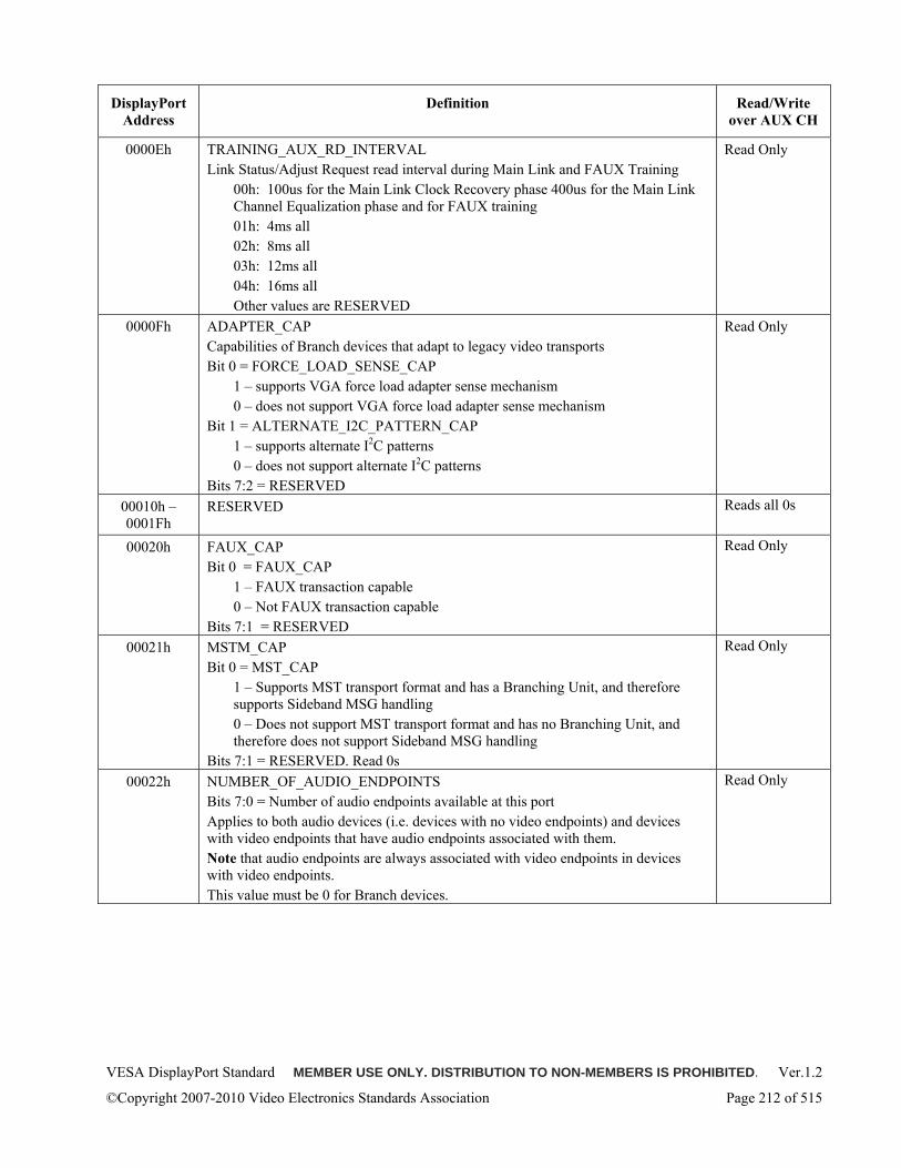
VESA DisplayPort Standard MEMBER USE ONLY. DISTRIBUTION TO NON-MEMBERS IS PROHIBITED. Ver.1.2
©Copyright 2007-2010 Video Electronics Standards Association Page 212 of 515
DisplayPort Address
Definition Read/Write over AUX CH
0000Eh TRAINING_AUX_RD_INTERVAL Link Status/Adjust Request read interval during Main Link and FAUX Training
00h: 100us for the Main Link Clock Recovery phase 400us for the Main Link Channel Equalization phase and for FAUX training 01h: 4ms all 02h: 8ms all 03h: 12ms all 04h: 16ms all Other values are RESERVED
Read Only
0000Fh ADAPTER_CAP Capabilities of Branch devices that adapt to legacy video transports Bit 0 = FORCE_LOAD_SENSE_CAP
1 – supports VGA force load adapter sense mechanism 0 – does not support VGA force load adapter sense mechanism
Bit 1 = ALTERNATE_I2C_PATTERN_CAP 1 – supports alternate I2C patterns 0 – does not support alternate I2C patterns
Bits 7:2 = RESERVED
Read Only
00010h – 0001Fh
RESERVED
Reads all 0s
00020h FAUX_CAP Bit 0 = FAUX_CAP
1 – FAUX transaction capable 0 – Not FAUX transaction capable
Bits 7:1 = RESERVED
Read Only
00021h MSTM_CAP Bit 0 = MST_CAP
1 – Supports MST transport format and has a Branching Unit, and therefore supports Sideband MSG handling 0 – Does not support MST transport format and has no Branching Unit, and therefore does not support Sideband MSG handling
Bits 7:1 = RESERVED. Read 0s
Read Only
00022h NUMBER_OF_AUDIO_ENDPOINTS Bits 7:0 = Number of audio endpoints available at this port Applies to both audio devices (i.e. devices with no video endpoints) and devices with video endpoints that have audio endpoints associated with them. Note that audio endpoints are always associated with video endpoints in devices with video endpoints. This value must be 0 for Branch devices.
Read Only
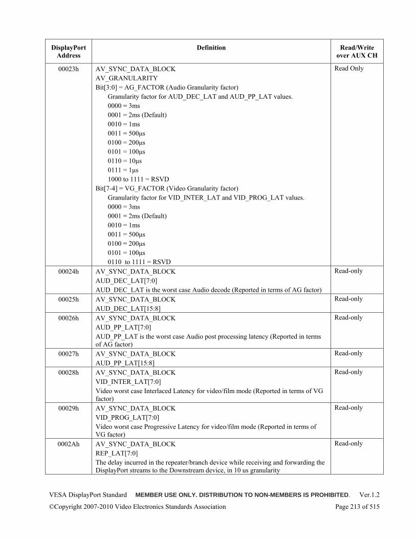
VESA DisplayPort Standard MEMBER USE ONLY. DISTRIBUTION TO NON-MEMBERS IS PROHIBITED. Ver.1.2
©Copyright 2007-2010 Video Electronics Standards Association Page 213 of 515
DisplayPort Address
Definition Read/Write over AUX CH
00023h AV_SYNC_DATA_BLOCK AV_GRANULARITY Bit[3:0] = AG_FACTOR (Audio Granularity factor)
Granularity factor for AUD_DEC_LAT and AUD_PP_LAT values. 0000 = 3ms 0001 = 2ms (Default) 0010 = 1ms 0011 = 500μs 0100 = 200μs 0101 = 100μs 0110 = 10μs 0111 = 1μs 1000 to 1111 = RSVD
Bit[7-4] = VG_FACTOR (Video Granularity factor) Granularity factor for VID_INTER_LAT and VID_PROG_LAT values. 0000 = 3ms 0001 = 2ms (Default) 0010 = 1ms 0011 = 500μs 0100 = 200μs 0101 = 100μs 0110 to 1111 = RSVD
Read Only
00024h AV_SYNC_DATA_BLOCK AUD_DEC_LAT[7:0] AUD_DEC_LAT is the worst case Audio decode (Reported in terms of AG factor)
Read-only
00025h AV_SYNC_DATA_BLOCK AUD_DEC_LAT[15:8]
Read-only
00026h AV_SYNC_DATA_BLOCK AUD_PP_LAT[7:0] AUD_PP_LAT is the worst case Audio post processing latency (Reported in terms of AG factor)
Read-only
00027h AV_SYNC_DATA_BLOCK AUD_PP_LAT[15:8]
Read-only
00028h AV_SYNC_DATA_BLOCK VID_INTER_LAT[7:0] Video worst case Interlaced Latency for video/film mode (Reported in terms of VG factor)
Read-only
00029h AV_SYNC_DATA_BLOCK VID_PROG_LAT[7:0] Video worst case Progressive Latency for video/film mode (Reported in terms of VG factor)
Read-only
0002Ah AV_SYNC_DATA_BLOCK REP_LAT[7:0] The delay incurred in the repeater/branch device while receiving and forwarding the DisplayPort streams to the Downstream device, in 10 us granularity
Read-only
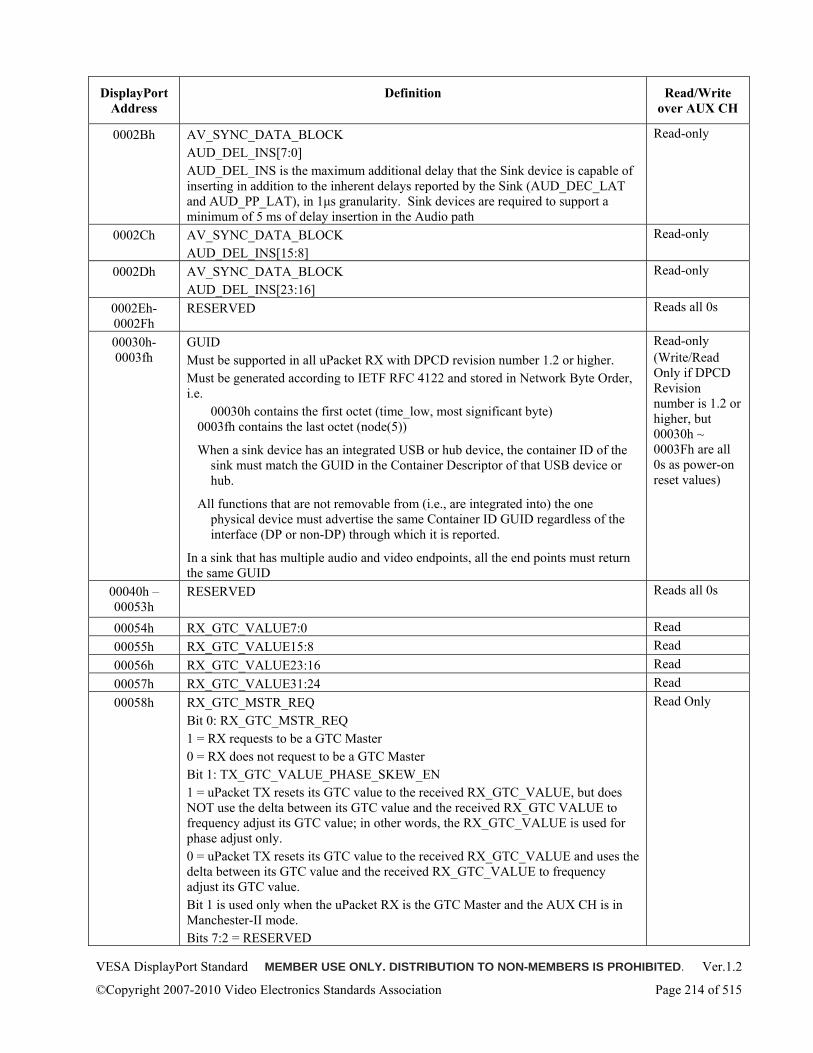
VESA DisplayPort Standard MEMBER USE ONLY. DISTRIBUTION TO NON-MEMBERS IS PROHIBITED. Ver.1.2
©Copyright 2007-2010 Video Electronics Standards Association Page 214 of 515
DisplayPort Address
Definition Read/Write over AUX CH
0002Bh AV_SYNC_DATA_BLOCK AUD_DEL_INS[7:0] AUD_DEL_INS is the maximum additional delay that the Sink device is capable of inserting in addition to the inherent delays reported by the Sink (AUD_DEC_LAT and AUD_PP_LAT), in 1μs granularity. Sink devices are required to support a minimum of 5 ms of delay insertion in the Audio path
Read-only
0002Ch AV_SYNC_DATA_BLOCK AUD_DEL_INS[15:8]
Read-only
0002Dh AV_SYNC_DATA_BLOCK AUD_DEL_INS[23:16]
Read-only
0002Eh-0002Fh
RESERVED Reads all 0s
00030h-0003fh
GUID Must be supported in all uPacket RX with DPCD revision number 1.2 or higher. Must be generated according to IETF RFC 4122 and stored in Network Byte Order, i.e.
00030h contains the first octet (time_low, most significant byte) 0003fh contains the last octet (node(5))
When a sink device has an integrated USB or hub device, the container ID of the sink must match the GUID in the Container Descriptor of that USB device or hub.
All functions that are not removable from (i.e., are integrated into) the one physical device must advertise the same Container ID GUID regardless of the interface (DP or non-DP) through which it is reported.
In a sink that has multiple audio and video endpoints, all the end points must return the same GUID
Read-only (Write/Read Only if DPCD Revision number is 1.2 or higher, but 00030h ~ 0003Fh are all 0s as power-on reset values)
00040h – 00053h
RESERVED
Reads all 0s
00054h RX_GTC_VALUE7:0 Read 00055h RX_GTC_VALUE15:8 Read 00056h RX_GTC_VALUE23:16 Read 00057h RX_GTC_VALUE31:24 Read 00058h RX_GTC_MSTR_REQ
Bit 0: RX_GTC_MSTR_REQ 1 = RX requests to be a GTC Master 0 = RX does not request to be a GTC Master Bit 1: TX_GTC_VALUE_PHASE_SKEW_EN 1 = uPacket TX resets its GTC value to the received RX_GTC_VALUE, but does NOT use the delta between its GTC value and the received RX_GTC VALUE to frequency adjust its GTC value; in other words, the RX_GTC_VALUE is used for phase adjust only. 0 = uPacket TX resets its GTC value to the received RX_GTC_VALUE and uses the delta between its GTC value and the received RX_GTC_VALUE to frequency adjust its GTC value. Bit 1 is used only when the uPacket RX is the GTC Master and the AUX CH is in Manchester-II mode. Bits 7:2 = RESERVED
Read Only
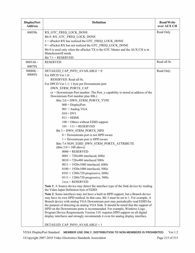
VESA DisplayPort Standard MEMBER USE ONLY. DISTRIBUTION TO NON-MEMBERS IS PROHIBITED. Ver.1.2
©Copyright 2007-2010 Video Electronics Standards Association Page 215 of 515
DisplayPort Address
Definition Read/Write over AUX CH
00059h RX_GTC_FREQ_LOCK_DONE Bit 0: RX_GTC_FREQ_LOCK_DONE 1 = uPacket RX has realized the GTC_FREQ_LOCK_DONE 0 = uPacket RX has not realized the GTC_FREQ_LOCK_DONE Bit 0 is used only when the uPacket TX is the GTC Master and the AUX CH is in MancheseterII mode. Bit 7:1 = RESERVED
Read Only
0005Ah – 0007Fh
RESERVED Read all 0s
00080h – 0008Fh
DETAILED_CAP_INFO_AVAILABLE = 0 For DPCD Ver.1.0:
RESERVED. Read all 0s. For DPCD Ver.1.1: 1 byte per Downstream port
DWN_STRM_PORTX_CAP (x = Downstream Port number. The Port_x capability is stored at address of the Downstream Port number plus 80h.)
Bits 2:0 = DWN_STRM_PORTX_TYPE 000 = DisplayPort 001 = Analog VGA 010 = DVI 011 = HDMI 100 = Others without EDID support 101 – 111 = RESERVED
Bit 3 = DWN_STRM_PORTX_HPD 0 = Downstream port is not HPD aware 1 = Downstream port is HPD aware
Bits 7:4 NON_EDID_DWN_STRM_PORTX_ATTRIBUTE (Bits 2:0 = 100 above)
0000 = RESERVED 0001 = 720x480 interlaced, 60Hz 0010 = 720x480 interlaced 50Hz 0011 = 1920x1080 interlaced, 60Hz 0100 = 1920x1080 interlaced, 50Hz 0101 = 1280x720 progressive, 60Hz 0111 = 1280x720 progressive, 50Hz 1xxx = RESERVED
Note 1: A Source device may detect the interface type of the Sink device by reading the Video Input Definition byte of EDID. Note 2: Some interfaces may not have a built-in HPD support, but a Branch device may have its own HPD method. In that case, Bit 3 must be set to 1. For example, A Branch device with analog VGA Downstream port may periodically read EDID for the purpose of detecting an analog VGA Sink. It should be noted that the support of HPD on the Downstream ports is recommended. For example, Windows Logo Program Device Requirements Version 3.01 requires HPD support on all digital display interfaces and strongly recommends it even for analog display interface. DETAILED_CAP_INFO_AVAILABLE = 1
Read Only
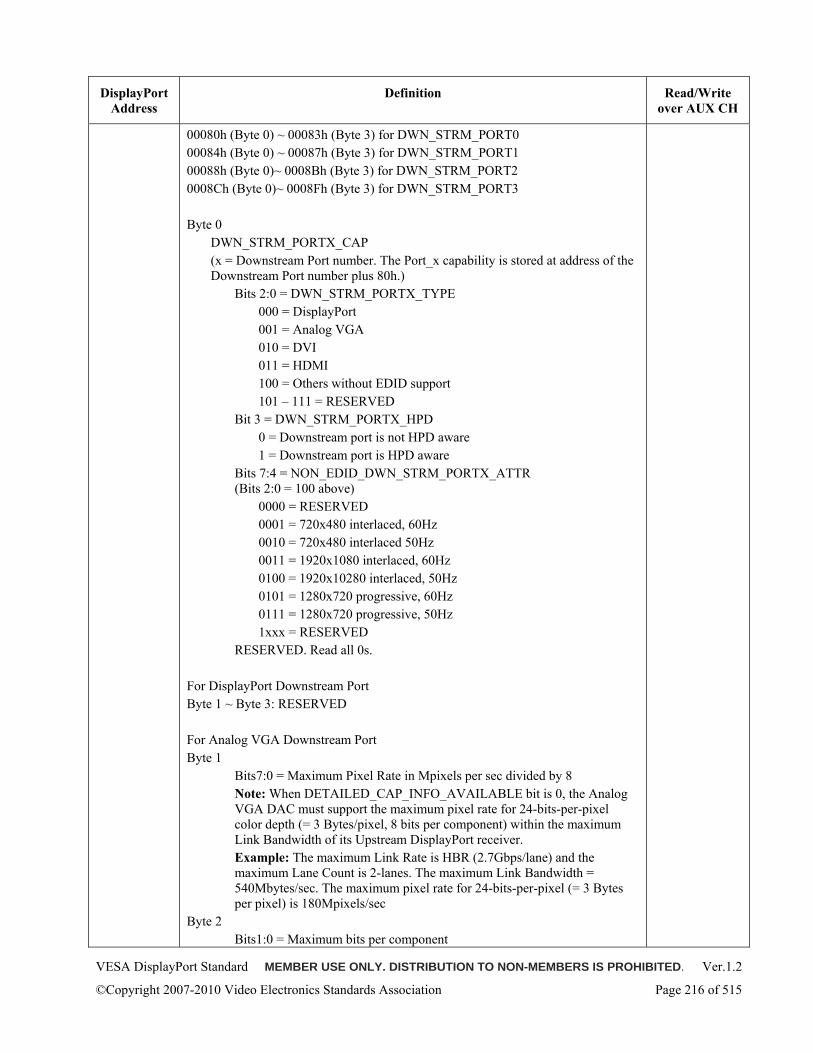
VESA DisplayPort Standard MEMBER USE ONLY. DISTRIBUTION TO NON-MEMBERS IS PROHIBITED. Ver.1.2
©Copyright 2007-2010 Video Electronics Standards Association Page 216 of 515
DisplayPort Address
Definition Read/Write over AUX CH
00080h (Byte 0) ~ 00083h (Byte 3) for DWN_STRM_PORT0 00084h (Byte 0) ~ 00087h (Byte 3) for DWN_STRM_PORT1 00088h (Byte 0)~ 0008Bh (Byte 3) for DWN_STRM_PORT2 0008Ch (Byte 0)~ 0008Fh (Byte 3) for DWN_STRM_PORT3 Byte 0
DWN_STRM_PORTX_CAP (x = Downstream Port number. The Port_x capability is stored at address of the Downstream Port number plus 80h.)
Bits 2:0 = DWN_STRM_PORTX_TYPE 000 = DisplayPort 001 = Analog VGA 010 = DVI 011 = HDMI 100 = Others without EDID support 101 – 111 = RESERVED
Bit 3 = DWN_STRM_PORTX_HPD 0 = Downstream port is not HPD aware 1 = Downstream port is HPD aware
Bits 7:4 = NON_EDID_DWN_STRM_PORTX_ATTR (Bits 2:0 = 100 above)
0000 = RESERVED 0001 = 720x480 interlaced, 60Hz 0010 = 720x480 interlaced 50Hz 0011 = 1920x1080 interlaced, 60Hz 0100 = 1920x10280 interlaced, 50Hz 0101 = 1280x720 progressive, 60Hz 0111 = 1280x720 progressive, 50Hz 1xxx = RESERVED
RESERVED. Read all 0s. For DisplayPort Downstream Port Byte 1 ~ Byte 3: RESERVED For Analog VGA Downstream Port Byte 1
Bits7:0 = Maximum Pixel Rate in Mpixels per sec divided by 8 Note: When DETAILED_CAP_INFO_AVAILABLE bit is 0, the Analog VGA DAC must support the maximum pixel rate for 24-bits-per-pixel color depth (= 3 Bytes/pixel, 8 bits per component) within the maximum Link Bandwidth of its Upstream DisplayPort receiver. Example: The maximum Link Rate is HBR (2.7Gbps/lane) and the maximum Lane Count is 2-lanes. The maximum Link Bandwidth = 540Mbytes/sec. The maximum pixel rate for 24-bits-per-pixel (= 3 Bytes per pixel) is 180Mpixels/sec
Byte 2 Bits1:0 = Maximum bits per component
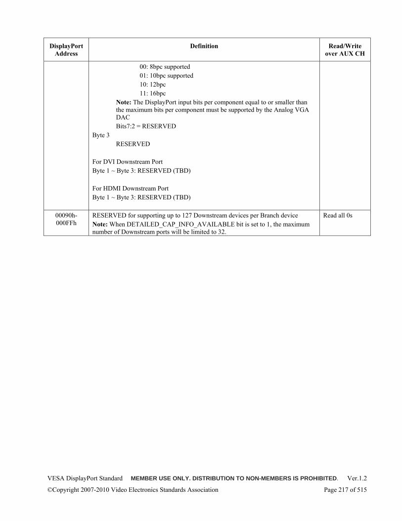
VESA DisplayPort Standard MEMBER USE ONLY. DISTRIBUTION TO NON-MEMBERS IS PROHIBITED. Ver.1.2
©Copyright 2007-2010 Video Electronics Standards Association Page 217 of 515
DisplayPort Address
Definition Read/Write over AUX CH
00: 8bpc supported 01: 10bpc supported 10: 12bpc 11: 16bpc
Note: The DisplayPort input bits per component equal to or smaller than the maximum bits per component must be supported by the Analog VGA DAC Bits7:2 = RESERVED
Byte 3 RESERVED
For DVI Downstream Port Byte 1 ~ Byte 3: RESERVED (TBD) For HDMI Downstream Port Byte 1 ~ Byte 3: RESERVED (TBD)
00090h- 000FFh
RESERVED for supporting up to 127 Downstream devices per Branch device Note: When DETAILED_CAP_INFO_AVAILABLE bit is set to 1, the maximum number of Downstream ports will be limited to 32.
Read all 0s
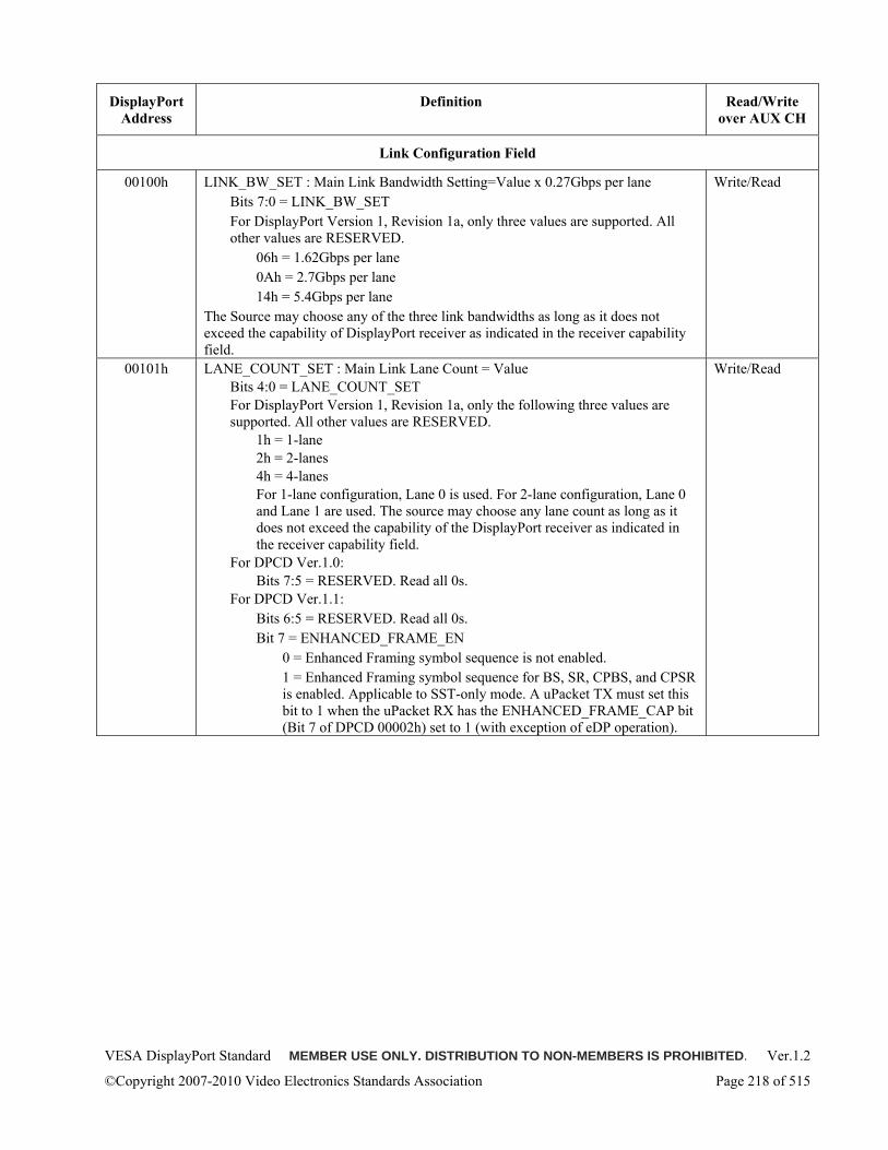
VESA DisplayPort Standard MEMBER USE ONLY. DISTRIBUTION TO NON-MEMBERS IS PROHIBITED. Ver.1.2
©Copyright 2007-2010 Video Electronics Standards Association Page 218 of 515
DisplayPort Address
Definition Read/Write over AUX CH
Link Configuration Field
00100h LINK_BW_SET : Main Link Bandwidth Setting=Value x 0.27Gbps per lane Bits 7:0 = LINK_BW_SET For DisplayPort Version 1, Revision 1a, only three values are supported. All other values are RESERVED.
06h = 1.62Gbps per lane 0Ah = 2.7Gbps per lane 14h = 5.4Gbps per lane
The Source may choose any of the three link bandwidths as long as it does not exceed the capability of DisplayPort receiver as indicated in the receiver capability field.
Write/Read
00101h LANE_COUNT_SET : Main Link Lane Count = Value Bits 4:0 = LANE_COUNT_SET For DisplayPort Version 1, Revision 1a, only the following three values are supported. All other values are RESERVED.
1h = 1-lane 2h = 2-lanes 4h = 4-lanes For 1-lane configuration, Lane 0 is used. For 2-lane configuration, Lane 0 and Lane 1 are used. The source may choose any lane count as long as it does not exceed the capability of the DisplayPort receiver as indicated in the receiver capability field.
For DPCD Ver.1.0: Bits 7:5 = RESERVED. Read all 0s.
For DPCD Ver.1.1: Bits 6:5 = RESERVED. Read all 0s. Bit 7 = ENHANCED_FRAME_EN
0 = Enhanced Framing symbol sequence is not enabled. 1 = Enhanced Framing symbol sequence for BS, SR, CPBS, and CPSR is enabled. Applicable to SST-only mode. A uPacket TX must set this bit to 1 when the uPacket RX has the ENHANCED_FRAME_CAP bit (Bit 7 of DPCD 00002h) set to 1 (with exception of eDP operation).
Write/Read
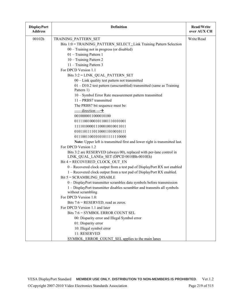
VESA DisplayPort Standard MEMBER USE ONLY. DISTRIBUTION TO NON-MEMBERS IS PROHIBITED. Ver.1.2
©Copyright 2007-2010 Video Electronics Standards Association Page 219 of 515
DisplayPort Address
Definition Read/Write over AUX CH
00102h TRAINING_PATTERN_SET Bits 1:0 = TRAINING_PATTERN_SELECT : Link Training Pattern Selection
00 – Training not in progress (or disabled) 01 – Training Pattern 1 10 – Training Pattern 2 11 – Training Pattern 3
For DPCD Version 1.1 Bits 3:2 = LINK_QUAL_PATTERN_SET
00 – Link quality test pattern not transmitted 01 – D10.2 test pattern (unscrambled) transmitted (same as Training Pattern 1) 10 – Symbol Error Rate measurement pattern transmitted 11 – PRBS7 transmitted The PRBS7 bit sequence must be: ----- direction --- 0010000011000010100 011110010001011001110101001 111101000011100010010011011 010110111101100011010010111 011100110010101011111110000 Note: Upper left is transmitted first and lower right is transmitted last.
For DPCD Version 1.2 Bits 3:2 are RESERVED (always 00), replaced with per-lane control in LINK_QUAL_LANEn_SET (DPCD 0010Bh-0010Eh)
Bit 4 = RECOVERED_CLOCK_OUT_EN 0 – Recovered clock output from a test pad of DisplayPort RX not enabled 1 – Recovered clock output from a test pad of DisplayPort RX enabled.
Bit 5 = SCRAMBLING_DISABLE 0 – DisplayPort transmitter scrambles data symbols before transmission 1 – DisplayPort transmitter disables scrambler and transmits all symbols without scrambling
For DPCD Version 1.0: Bits 7:6 = RESERVED, read as zeros.
For DPCD Version 1.1 and later Bits 7:6 = SYMBOL ERROR COUNT SEL
00: Disparity error and Illegal Symbol error 01: Disparity error 10: Illegal symbol error 11: RESERVED
SYMBOL_ERROR_COUNT_SEL applies to the main lanes
Write/Read
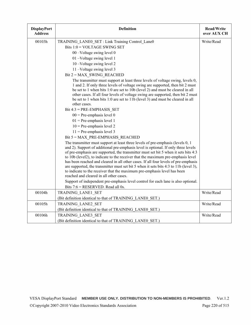
VESA DisplayPort Standard MEMBER USE ONLY. DISTRIBUTION TO NON-MEMBERS IS PROHIBITED. Ver.1.2
©Copyright 2007-2010 Video Electronics Standards Association Page 220 of 515
DisplayPort Address
Definition Read/Write over AUX CH
00103h TRAINING_LANE0_SET : Link Training Control_Lane0 Bits 1:0 = VOLTAGE SWING SET
00 –Voltage swing level 0 01 –Voltage swing level 1 10 –Voltage swing level 2 11 –Voltage swing level 3
Bit 2 = MAX_SWING_REACHED The transmitter must support at least three levels of voltage swing, levels 0, 1 and 2. If only three levels of voltage swing are supported, then bit 2 must be set to 1 when bits 1:0 are set to 10b (level 2) and must be cleared in all other cases. If all four levels of voltage swing are supported, then bit 2 must be set to 1 when bits 1:0 are set to 11b (level 3) and must be cleared in all other cases.
Bit 4:3 = PRE-EMPHASIS_SET 00 = Pre-emphasis level 0 01 = Pre-emphasis level 1 10 = Pre-emphasis level 2 11 = Pre-emphasis level 3
Bit 5 = MAX_PRE-EMPHASIS_REACHED The transmitter must support at least three levels of pre-emphasis (levels 0, 1 and 2). Support of additional pre-emphasis level is optional. If only three levels of pre-emphasis are supported, the transmitter must set bit 5 when it sets bits 4:3 to 10b (level2), to indicate to the receiver that the maximum pre-emphasis level has been reached and cleared in all other cases. If all four levels of pre-emphasis are supported, the transmitter must set bit 5 when it sets bits 4:3 to 11b (level 3), to indicate to the receiver that the maximum pre-emphasis level has been reached and cleared in all other cases. Support of independent pre-emphasis level control for each lane is also optional. Bits 7:6 = RESERVED. Read all 0s.
Write/Read
00104h TRAINING_LANE1_SET (Bit definition identical to that of TRAINING_LANE0_SET.)
Write/Read
00105h TRAINING_LANE2_SET (Bit definition identical to that of TRAINING_LANE0_SET.)
Write/Read
00106h TRAINING_LANE3_SET (Bit definition identical to that of TRAINING_LANE0_SET.)
Write/Read
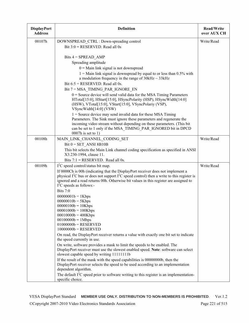
VESA DisplayPort Standard MEMBER USE ONLY. DISTRIBUTION TO NON-MEMBERS IS PROHIBITED. Ver.1.2
©Copyright 2007-2010 Video Electronics Standards Association Page 221 of 515
DisplayPort Address
Definition Read/Write over AUX CH
00107h DOWNSPREAD_CTRL : Down-spreading control Bit 3:0 = RESERVED. Read all 0s Bits 4 = SPREAD_AMP
Spreading amplitude 0 = Main link signal is not downspread 1 = Main link signal is downspread by equal to or less than 0.5% with a modulation frequency in the range of 30kHz ~ 33kHz
Bit 6:5 = RESERVED. Read all 0s. Bit 7 = MSA_TIMING_PAR_IGNORE_EN
0 = Source device will send valid data for the MSA Timing Parameters HTotal[15:0], HStart[15:0], HSyncPolarity (HSP), HSyncWidth[14:0] (HSW), VTotal[15:0], VStart[15:0], VSyncPolariy (VSP), VSyncWidth[14:0] (VSW) 1 = Source device may send invalid data for these MSA Timing Parameters. The Sink must ignore these parameters and regenerate the incoming video stream without depending on these parameters. (This bit can be set to 1 only if the MSA_TIMING_PAR_IGNORED bit in DPCD 0007h is set to 1)
Write/Read
00108h MAIN_LINK_CHANNEL_CODING_SET Bit 0 = SET_ANSI 8B10B This bit selects the Main Link channel coding specification as specified in ANSI X3.230-1994, clause 11. Bits 7:1 = RESERVED. Read all 0s.
Write/Read
00109h I2C speed control/status bit map. If 0000Ch is 00h (indicating that the DisplayPort receiver does not implement a physical I2C bus or does not support I2C speed control) then a write to this register is ignored and a read returns 00h. Otherwise bit values in this register are assigned to I2C speeds as follows:- Bits 7:0 00000001b = 1Kbps 00000010b = 5Kbps 00000100b = 10Kbps 00001000b = 100Kbps 00010000b = 400Kbps 00100000b = 1Mbps 01000000b = RESERVED 10000000b = RESERVED On read, the DisplayPort receiver returns a value with exactly one bit set to indicate the speed currently in use. On write, software provides a mask to limit the speeds to be enabled. The DisplayPort receiver must use the slowest enabled speed. Note: software can select slowest capable speed by writing 11111111b If the result of the mask with the speed capabilities is 00000000b, then the DisplayPort receiver selects the speed to be used according to an implementation dependent algorithm. The default I2C speed prior to software writing to this register is an implementation-specific choice.
Write/Read
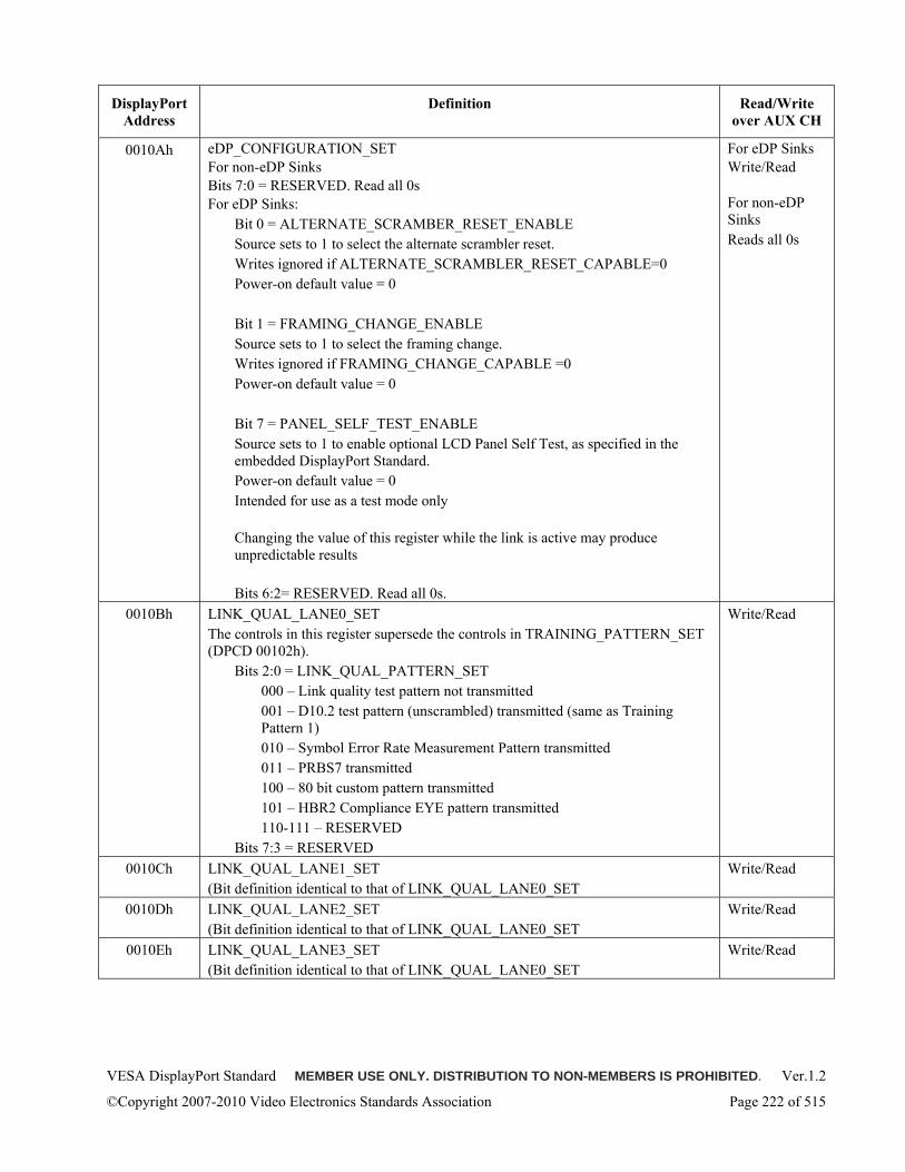
VESA DisplayPort Standard MEMBER USE ONLY. DISTRIBUTION TO NON-MEMBERS IS PROHIBITED. Ver.1.2
©Copyright 2007-2010 Video Electronics Standards Association Page 222 of 515
DisplayPort Address
Definition Read/Write over AUX CH
0010Ah eDP_CONFIGURATION_SET For non-eDP Sinks Bits 7:0 = RESERVED. Read all 0s For eDP Sinks:
Bit 0 = ALTERNATE_SCRAMBER_RESET_ENABLE Source sets to 1 to select the alternate scrambler reset. Writes ignored if ALTERNATE_SCRAMBLER_RESET_CAPABLE=0 Power-on default value = 0 Bit 1 = FRAMING_CHANGE_ENABLE Source sets to 1 to select the framing change. Writes ignored if FRAMING_CHANGE_CAPABLE =0 Power-on default value = 0
Bit 7 = PANEL_SELF_TEST_ENABLE Source sets to 1 to enable optional LCD Panel Self Test, as specified in the embedded DisplayPort Standard. Power-on default value = 0 Intended for use as a test mode only
Changing the value of this register while the link is active may produce unpredictable results Bits 6:2= RESERVED. Read all 0s.
For eDP Sinks Write/Read For non-eDP Sinks Reads all 0s
0010Bh LINK_QUAL_LANE0_SET The controls in this register supersede the controls in TRAINING_PATTERN_SET (DPCD 00102h).
Bits 2:0 = LINK_QUAL_PATTERN_SET 000 – Link quality test pattern not transmitted 001 – D10.2 test pattern (unscrambled) transmitted (same as Training Pattern 1) 010 – Symbol Error Rate Measurement Pattern transmitted 011 – PRBS7 transmitted 100 – 80 bit custom pattern transmitted 101 – HBR2 Compliance EYE pattern transmitted 110-111 – RESERVED
Bits 7:3 = RESERVED
Write/Read
0010Ch LINK_QUAL_LANE1_SET (Bit definition identical to that of LINK_QUAL_LANE0_SET
Write/Read
0010Dh LINK_QUAL_LANE2_SET (Bit definition identical to that of LINK_QUAL_LANE0_SET
Write/Read
0010Eh LINK_QUAL_LANE3_SET (Bit definition identical to that of LINK_QUAL_LANE0_SET
Write/Read
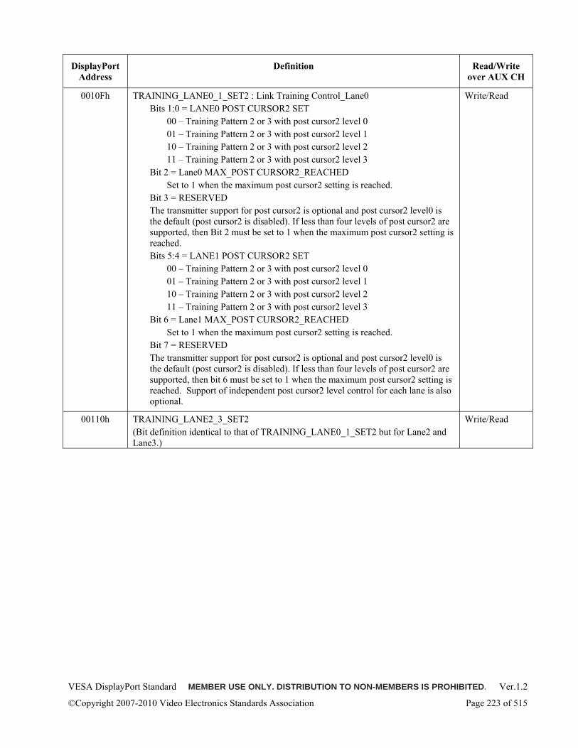
VESA DisplayPort Standard MEMBER USE ONLY. DISTRIBUTION TO NON-MEMBERS IS PROHIBITED. Ver.1.2
©Copyright 2007-2010 Video Electronics Standards Association Page 223 of 515
DisplayPort Address
Definition Read/Write over AUX CH
0010Fh TRAINING_LANE0_1_SET2 : Link Training Control_Lane0 Bits 1:0 = LANE0 POST CURSOR2 SET
00 – Training Pattern 2 or 3 with post cursor2 level 0 01 – Training Pattern 2 or 3 with post cursor2 level 1 10 – Training Pattern 2 or 3 with post cursor2 level 2 11 – Training Pattern 2 or 3 with post cursor2 level 3
Bit 2 = Lane0 MAX_POST CURSOR2_REACHED Set to 1 when the maximum post cursor2 setting is reached.
Bit 3 = RESERVED The transmitter support for post cursor2 is optional and post cursor2 level0 is the default (post cursor2 is disabled). If less than four levels of post cursor2 are supported, then Bit 2 must be set to 1 when the maximum post cursor2 setting is reached. Bits 5:4 = LANE1 POST CURSOR2 SET
00 – Training Pattern 2 or 3 with post cursor2 level 0 01 – Training Pattern 2 or 3 with post cursor2 level 1 10 – Training Pattern 2 or 3 with post cursor2 level 2 11 – Training Pattern 2 or 3 with post cursor2 level 3
Bit 6 = Lane1 MAX_POST CURSOR2_REACHED Set to 1 when the maximum post cursor2 setting is reached.
Bit 7 = RESERVED The transmitter support for post cursor2 is optional and post cursor2 level0 is the default (post cursor2 is disabled). If less than four levels of post cursor2 are supported, then bit 6 must be set to 1 when the maximum post cursor2 setting is reached. Support of independent post cursor2 level control for each lane is also optional.
Write/Read
00110h TRAINING_LANE2_3_SET2 (Bit definition identical to that of TRAINING_LANE0_1_SET2 but for Lane2 and Lane3.)
Write/Read
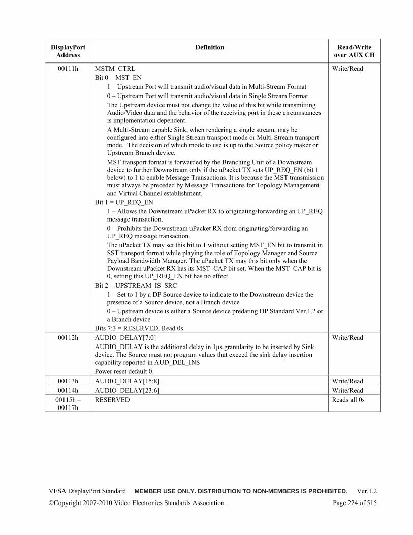
VESA DisplayPort Standard MEMBER USE ONLY. DISTRIBUTION TO NON-MEMBERS IS PROHIBITED. Ver.1.2
©Copyright 2007-2010 Video Electronics Standards Association Page 224 of 515
DisplayPort Address
Definition Read/Write over AUX CH
00111h MSTM_CTRL Bit 0 = MST_EN
1 – Upstream Port will transmit audio/visual data in Multi-Stream Format 0 – Upstream Port will transmit audio/visual data in Single Stream Format The Upstream device must not change the value of this bit while transmitting Audio/Video data and the behavior of the receiving port in these circumstances is implementation dependent. A Multi-Stream capable Sink, when rendering a single stream, may be configured into either Single Stream transport mode or Multi-Stream transport mode. The decision of which mode to use is up to the Source policy maker or Upstream Branch device. MST transport format is forwarded by the Branching Unit of a Downstream device to further Downstream only if the uPacket TX sets UP_REQ_EN (bit 1 below) to 1 to enable Message Transactions. It is because the MST transmission must always be preceded by Message Transactions for Topology Management and Virtual Channel establishment.
Bit 1 = UP_REQ_EN 1 – Allows the Downstream uPacket RX to originating/forwarding an UP_REQ message transaction. 0 – Prohibits the Downstream uPacket RX from originating/forwarding an UP_REQ message transaction. The uPacket TX may set this bit to 1 without setting MST_EN bit to transmit in SST transport format while playing the role of Topology Manager and Source Payload Bandwidth Manager. The uPacket TX may this bit only when the Downstream uPacket RX has its MST_CAP bit set. When the MST_CAP bit is 0, setting this UP_REQ_EN bit has no effect.
Bit 2 = UPSTREAM_IS_SRC 1 – Set to 1 by a DP Source device to indicate to the Downstream device the presence of a Source device, not a Branch device 0 – Upstream device is either a Source device predating DP Standard Ver.1.2 or a Branch device
Bits 7:3 = RESERVED. Read 0s
Write/Read
00112h AUDIO_DELAY[7:0] AUDIO_DELAY is the additional delay in 1μs granularity to be inserted by Sink device. The Source must not program values that exceed the sink delay insertion capability reported in AUD_DEL_INS Power reset default 0.
Write/Read
00113h AUDIO_DELAY[15:8] Write/Read 00114h AUDIO_DELAY[23:6] Write/Read
00115h – 00117h
RESERVED Reads all 0s
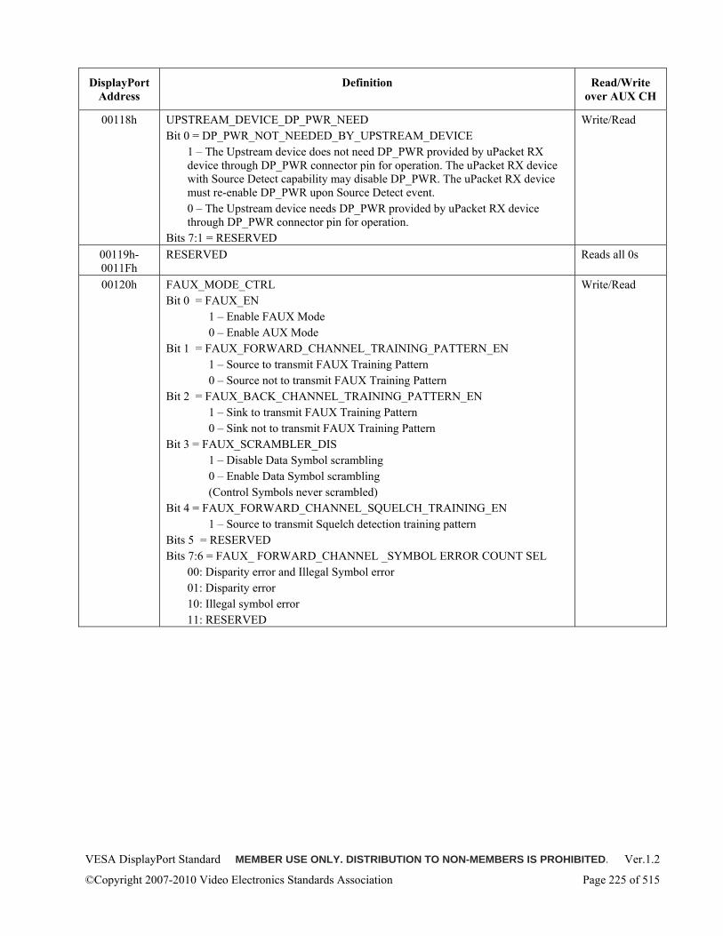
VESA DisplayPort Standard MEMBER USE ONLY. DISTRIBUTION TO NON-MEMBERS IS PROHIBITED. Ver.1.2
©Copyright 2007-2010 Video Electronics Standards Association Page 225 of 515
DisplayPort Address
Definition Read/Write over AUX CH
00118h UPSTREAM_DEVICE_DP_PWR_NEED Bit 0 = DP_PWR_NOT_NEEDED_BY_UPSTREAM_DEVICE
1 – The Upstream device does not need DP_PWR provided by uPacket RX device through DP_PWR connector pin for operation. The uPacket RX device with Source Detect capability may disable DP_PWR. The uPacket RX device must re-enable DP_PWR upon Source Detect event. 0 – The Upstream device needs DP_PWR provided by uPacket RX device through DP_PWR connector pin for operation.
Bits 7:1 = RESERVED
Write/Read
00119h- 0011Fh
RESERVED Reads all 0s
00120h FAUX_MODE_CTRL Bit 0 = FAUX_EN
1 – Enable FAUX Mode 0 – Enable AUX Mode
Bit 1 = FAUX_FORWARD_CHANNEL_TRAINING_PATTERN_EN 1 – Source to transmit FAUX Training Pattern 0 – Source not to transmit FAUX Training Pattern
Bit 2 = FAUX_BACK_CHANNEL_TRAINING_PATTERN_EN 1 – Sink to transmit FAUX Training Pattern 0 – Sink not to transmit FAUX Training Pattern
Bit 3 = FAUX_SCRAMBLER_DIS 1 – Disable Data Symbol scrambling 0 – Enable Data Symbol scrambling (Control Symbols never scrambled)
Bit 4 = FAUX_FORWARD_CHANNEL_SQUELCH_TRAINING_EN 1 – Source to transmit Squelch detection training pattern
Bits 5 = RESERVED Bits 7:6 = FAUX_ FORWARD_CHANNEL _SYMBOL ERROR COUNT SEL
00: Disparity error and Illegal Symbol error 01: Disparity error 10: Illegal symbol error 11: RESERVED
Write/Read
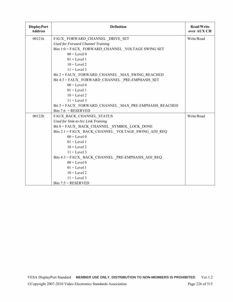
VESA DisplayPort Standard MEMBER USE ONLY. DISTRIBUTION TO NON-MEMBERS IS PROHIBITED. Ver.1.2
©Copyright 2007-2010 Video Electronics Standards Association Page 226 of 515
DisplayPort Address
Definition Read/Write over AUX CH
00121h FAUX_ FORWARD_CHANNEL _DRIVE_SET Used for Forward Channel Training Bits 1:0 = FAUX_ FORWARD_CHANNEL _VOLTAGE SWING SET
00 = Level 0 01 = Level 1 10 = Level 2 11 = Level 3
Bit 2 = FAUX_ FORWARD_CHANNEL _MAX_SWING_REACHED Bit 4:3 = FAUX_ FORWARD_CHANNEL _PRE-EMPHASIS_SET
00 = Level 0 01 = Level 1 10 = Level 2 11 = Level 3
Bit 5 = FAUX_ FORWARD_CHANNEL _MAX_PRE-EMPHASIS_REACHED Bits 7:6 = RESERVED
Write/Read
00122h FAUX_BACK_CHANNEL_STATUS Used for Sink-to-Src Link Training Bit 0 = FAUX_ BACK_CHANNEL _SYMBOL_LOCK_DONE Bits 2:1 = FAUX_ BACK_CHANNEL _VOLTAGE_SWING_ADJ_REQ
00 = Level 0 01 = Level 1 10 = Level 2 11 = Level 3
Bits 4:3 = FAUX_ BACK_CHANNEL _PRE-EMPHASIS_ADJ_REQ 00 = Level 0 01 = Level 1 10 = Level 2 11 = Level 3
Bits 7:5 = RESERVED
Write/Read
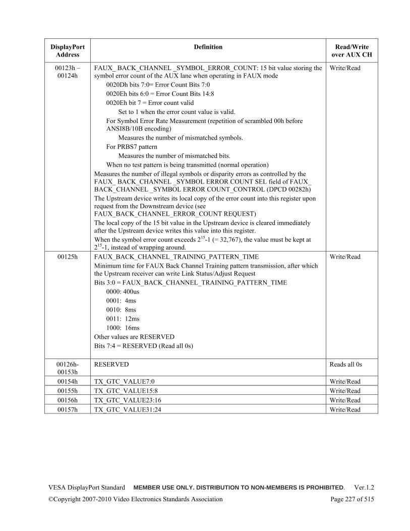
VESA DisplayPort Standard MEMBER USE ONLY. DISTRIBUTION TO NON-MEMBERS IS PROHIBITED. Ver.1.2
©Copyright 2007-2010 Video Electronics Standards Association Page 227 of 515
DisplayPort Address
Definition Read/Write over AUX CH
00123h – 00124h
FAUX_ BACK_CHANNEL _SYMBOL_ERROR_COUNT: 15 bit value storing the symbol error count of the AUX lane when operating in FAUX mode
0020Dh bits 7:0= Error Count Bits 7:0 0020Eh bits 6:0 = Error Count Bits 14:8 0020Eh bit 7 = Error count valid
Set to 1 when the error count value is valid. For Symbol Error Rate Measurement (repetition of scrambled 00h before ANSI8B/10B encoding)
Measures the number of mismatched symbols. For PRBS7 pattern
Measures the number of mismatched bits. When no test pattern is being transmitted (normal operation)
Measures the number of illegal symbols or disparity errors as controlled by the FAUX_ BACK_CHANNEL _SYMBOL ERROR COUNT SEL field of FAUX_ BACK_CHANNEL _SYMBOL ERROR COUNT_CONTROL (DPCD 00282h) The Upstream device writes its local copy of the error count into this register upon request from the Downstream device (see FAUX_BACK_CHANNEL_ERROR_COUNT REQUEST) The local copy of the 15 bit value in the Upstream device is cleared immediately after the Upstream device writes this value into this register. When the symbol error count exceeds 215-1 (= 32,767), the value must be kept at 215-1, instead of wrapping around.
Write/Read
00125h FAUX_BACK_CHANNEL_TRAINING_PATTERN_TIME Minimum time for FAUX Back Channel Training pattern transmission, after which the Upstream receiver can write Link Status/Adjust Request Bits 3:0 = FAUX_BACK_CHANNEL_TRAINING_PATTERN_TIME
0000: 400us 0001: 4ms 0010: 8ms 0011: 12ms 1000: 16ms
Other values are RESERVED Bits 7:4 = RESERVED (Read all 0s)
Write/Read
00126h- 00153h
RESERVED Reads all 0s
00154h TX_GTC_VALUE7:0 Write/Read 00155h TX_GTC_VALUE15:8 Write/Read 00156h TX_GTC_VALUE23:16 Write/Read 00157h TX_GTC_VALUE31:24 Write/Read
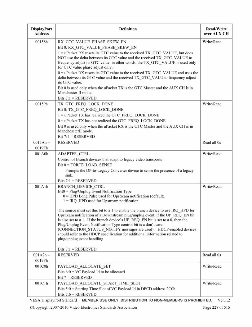
VESA DisplayPort Standard MEMBER USE ONLY. DISTRIBUTION TO NON-MEMBERS IS PROHIBITED. Ver.1.2
©Copyright 2007-2010 Video Electronics Standards Association Page 228 of 515
DisplayPort Address
Definition Read/Write over AUX CH
00158h RX_GTC_VALUE_PHASE_SKEW_EN Bit 0: RX_GTC_VALUE_PHASE_SKEW_EN 1 = uPacket RX resets its GTC value to the received TX_GTC_VALUE, but does NOT use the delta between its GTC value and the received TX_GTC_VALUE to frequency adjust its GTC value; in other words, the TX_GTC_VALUE is used only for GTC value phase adjust only. 0 = uPacket RX resets its GTC value to the received TX_GTC_VALUE and uses the delta between its GTC value and the received TX_GTC_VALU to frequency adjust its GTC value. Bit 0 is used only when the uPacket TX is the GTC Master and the AUX CH is in Manchester-II mode. Bits 7:1 = RESERVED.
Write/Read
00159h TX_GTC_FREQ_LOCK_DONE Bit 0: TX_GTC_FREQ_LOCK_DONE 1 = uPacket TX has realized the GTC_FREQ_LOCK_DONE 0 = uPacket TX has not realized the GTC_FREQ_LOCK_DONE Bit 0 is used only when the uPacket RX is the GTC Master and the AUX CH is in MancheseterII mode. Bit 7:1 = RESERVED
Write/Read
0015Ah – 0019Fh
RESERVED Read all 0s
001A0h ADAPTER_CTRL Control of Branch devices that adapt to legacy video transports Bit 0 = FORCE_LOAD_SENSE
Prompts the DP-to-Legacy Converter device to sense the presence of a legacy sink.
Bits 7:1 = RESERVED
Write/Read
001A1h BRANCH_DEVICE_CTRL Bit0 = Plug/Unplug Event Notification Type 0 = HPD Long Pulse used for Upstream notification (default). 1 = IRQ_HPD used for Upstream notification The source must set this bit to a 1 to enable the branch device to use IRQ_HPD for Upstream notification of a Downstream plug/unplug event, if the UP_REQ_EN bit is also set to a 1. If the branch device’s UP_REQ_EN bit is set to a 0, then the Plug/Unplug Event Notification Type control bit is a don’t care (CONNECTION_STATUS_NOTIFY messages are used). HDCP-enabled devices should refer to the HDCP specification for additional information related to plug/unplug event handling. Bits 7:1 = RESERVED
Write/Read
001A2h – 0019Fh
RESERVED Read all 0s
001C0h PAYLOAD_ALLOCATE_SET Bits 6:0 = VC Payload Id to be allocated Bit 7 = RESERVED
Write/Read
001C1h PAYLOAD_ALLOCATE_START_TIME_SLOT Bits 5:0 = Starting Time Slot of VC Payload Id in DPCD address 2C0h Bits 7:6 = RESERVED
Write/Read
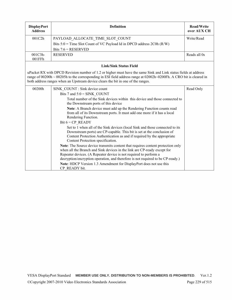
VESA DisplayPort Standard MEMBER USE ONLY. DISTRIBUTION TO NON-MEMBERS IS PROHIBITED. Ver.1.2
©Copyright 2007-2010 Video Electronics Standards Association Page 229 of 515
DisplayPort Address
Definition Read/Write over AUX CH
001C2h PAYLOAD_ALLOCATE_TIME_SLOT_COUNT Bits 5:0 = Time Slot Count of VC Payload Id in DPCD address 2C0h (R/W) Bits 7:6 = RESERVED
Write/Read
001C3h- 001FFh
RESERVED Reads all 0s
Link/Sink Status Field
uPacket RX with DPCD Revision number of 1.2 or higher must have the same Sink and Link status fields at address range of 00200h ~ 00205h to the corresponding in ESI field address range at 02002h~0200Fh. A CRO bit is cleared in both address ranges when an Upstream device clears the bit in one of the ranges.
00200h SINK_COUNT : Sink device count Bits 7 and 5:0 = SINK_COUNT
Total number of the Sink devices within this device and those connected to the Downstream ports of this device Note: A Branch device must add up the Rendering Function counts read from all of its Downstream ports. It must add one more if it has a local Rendering Function.
Bit 6 = CP_READY Set to 1 when all of the Sink devices (local Sink and those connected to its Downstream ports) are CP-capable. This bit is set at the conclusion of Content Protection Authentication as and if required by the appropriate Content Protection specification.
Note: The Source device transmits content that requires content protection only when all the Branch and Sink devices in the link are CP-ready except for Repeater devices. (A Repeater device is not required to perform a decryption/encryption operation, and therefore is not required to be CP-ready.) Note: HDCP Version 1.3 Amendment for DisplayPort does not use this CP_READY bit.
Read Only
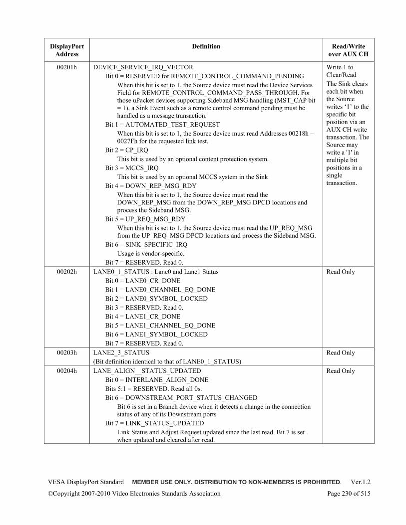
VESA DisplayPort Standard MEMBER USE ONLY. DISTRIBUTION TO NON-MEMBERS IS PROHIBITED. Ver.1.2
©Copyright 2007-2010 Video Electronics Standards Association Page 230 of 515
DisplayPort Address
Definition Read/Write over AUX CH
00201h DEVICE_SERVICE_IRQ_VECTOR Bit 0 = RESERVED for REMOTE_CONTROL_COMMAND_PENDING
When this bit is set to 1, the Source device must read the Device Services Field for REMOTE_CONTROL_COMMAND_PASS_THROUGH. For those uPacket devices supporting Sideband MSG handling (MST_CAP bit = 1), a Sink Event such as a remote control command pending must be handled as a message transaction.
Bit 1 = AUTOMATED_TEST_REQUEST When this bit is set to 1, the Source device must read Addresses 00218h – 0027Fh for the requested link test.
Bit 2 = CP_IRQ This bit is used by an optional content protection system.
Bit 3 = MCCS_IRQ This bit is used by an optional MCCS system in the Sink
Bit 4 = DOWN_REP_MSG_RDY When this bit is set to 1, the Source device must read the DOWN_REP_MSG from the DOWN_REP_MSG DPCD locations and process the Sideband MSG.
Bit 5 = UP_REQ_MSG_RDY When this bit is set to 1, the Source device must read the UP_REQ_MSG from the UP_REQ_MSG DPCD locations and process the Sideband MSG.
Bit 6 = SINK_SPECIFIC_IRQ Usage is vendor-specific.
Bit 7 = RESERVED. Read 0.
Write 1 to Clear/Read The Sink clears each bit when the Source writes ‘1’ to the specific bit position via an AUX CH write transaction. The Source may write a '1' in multiple bit positions in a single transaction.
00202h LANE0_1_STATUS : Lane0 and Lane1 Status Bit 0 = LANE0_CR_DONE Bit 1 = LANE0_CHANNEL_EQ_DONE Bit 2 = LANE0_SYMBOL_LOCKED Bit 3 = RESERVED. Read 0. Bit 4 = LANE1_CR_DONE Bit 5 = LANE1_CHANNEL_EQ_DONE Bit 6 = LANE1_SYMBOL_LOCKED Bit 7 = RESERVED. Read 0.
Read Only
00203h LANE2_3_STATUS (Bit definition identical to that of LANE0_1_STATUS)
Read Only
00204h LANE_ALIGN__STATUS_UPDATED Bit 0 = INTERLANE_ALIGN_DONE Bits 5:1 = RESERVED. Read all 0s. Bit 6 = DOWNSTREAM_PORT_STATUS_CHANGED
Bit 6 is set in a Branch device when it detects a change in the connection status of any of its Downstream ports
Bit 7 = LINK_STATUS_UPDATED Link Status and Adjust Request updated since the last read. Bit 7 is set when updated and cleared after read.
Read Only
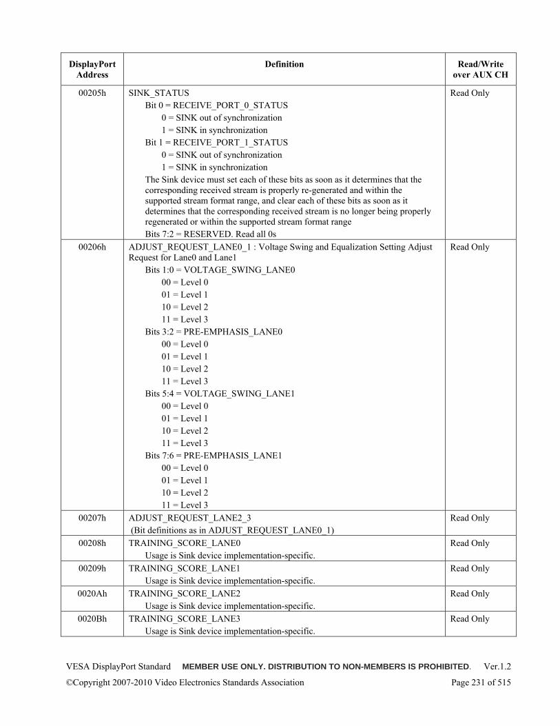
VESA DisplayPort Standard MEMBER USE ONLY. DISTRIBUTION TO NON-MEMBERS IS PROHIBITED. Ver.1.2
©Copyright 2007-2010 Video Electronics Standards Association Page 231 of 515
DisplayPort Address
Definition Read/Write over AUX CH
00205h SINK_STATUS Bit 0 = RECEIVE_PORT_0_STATUS
0 = SINK out of synchronization 1 = SINK in synchronization
Bit 1 = RECEIVE_PORT_1_STATUS 0 = SINK out of synchronization 1 = SINK in synchronization
The Sink device must set each of these bits as soon as it determines that the corresponding received stream is properly re-generated and within the supported stream format range, and clear each of these bits as soon as it determines that the corresponding received stream is no longer being properly regenerated or within the supported stream format range Bits 7:2 = RESERVED. Read all 0s
Read Only
00206h ADJUST_REQUEST_LANE0_1 : Voltage Swing and Equalization Setting Adjust Request for Lane0 and Lane1
Bits 1:0 = VOLTAGE_SWING_LANE0 00 = Level 0 01 = Level 1 10 = Level 2 11 = Level 3
Bits 3:2 = PRE-EMPHASIS_LANE0 00 = Level 0 01 = Level 1 10 = Level 2 11 = Level 3
Bits 5:4 = VOLTAGE_SWING_LANE1 00 = Level 0 01 = Level 1 10 = Level 2 11 = Level 3
Bits 7:6 = PRE-EMPHASIS_LANE1 00 = Level 0 01 = Level 1 10 = Level 2 11 = Level 3
Read Only
00207h ADJUST_REQUEST_LANE2_3 (Bit definitions as in ADJUST_REQUEST_LANE0_1)
Read Only
00208h TRAINING_SCORE_LANE0 Usage is Sink device implementation-specific.
Read Only
00209h TRAINING_SCORE_LANE1 Usage is Sink device implementation-specific.
Read Only
0020Ah TRAINING_SCORE_LANE2 Usage is Sink device implementation-specific.
Read Only
0020Bh TRAINING_SCORE_LANE3 Usage is Sink device implementation-specific.
Read Only
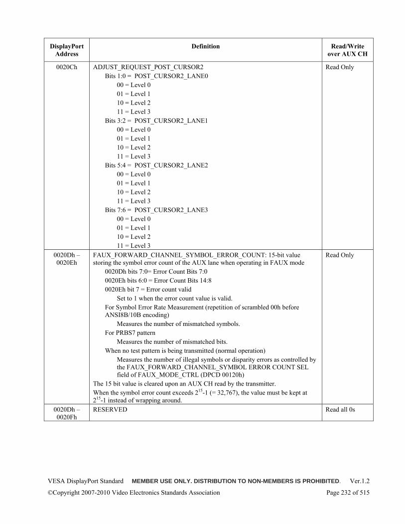
VESA DisplayPort Standard MEMBER USE ONLY. DISTRIBUTION TO NON-MEMBERS IS PROHIBITED. Ver.1.2
©Copyright 2007-2010 Video Electronics Standards Association Page 232 of 515
DisplayPort Address
Definition Read/Write over AUX CH
0020Ch ADJUST_REQUEST_POST_CURSOR2 Bits 1:0 = POST_CURSOR2_LANE0
00 = Level 0 01 = Level 1 10 = Level 2 11 = Level 3
Bits 3:2 = POST_CURSOR2_LANE1 00 = Level 0 01 = Level 1 10 = Level 2 11 = Level 3
Bits 5:4 = POST_CURSOR2_LANE2 00 = Level 0 01 = Level 1 10 = Level 2 11 = Level 3
Bits 7:6 = POST_CURSOR2_LANE3 00 = Level 0 01 = Level 1 10 = Level 2 11 = Level 3
Read Only
0020Dh – 0020Eh
FAUX_FORWARD_CHANNEL_SYMBOL_ERROR_COUNT: 15-bit value storing the symbol error count of the AUX lane when operating in FAUX mode
0020Dh bits 7:0= Error Count Bits 7:0 0020Eh bits 6:0 = Error Count Bits 14:8 0020Eh bit 7 = Error count valid
Set to 1 when the error count value is valid. For Symbol Error Rate Measurement (repetition of scrambled 00h before ANSI8B/10B encoding)
Measures the number of mismatched symbols. For PRBS7 pattern
Measures the number of mismatched bits. When no test pattern is being transmitted (normal operation)
Measures the number of illegal symbols or disparity errors as controlled by the FAUX_FORWARD_CHANNEL_SYMBOL ERROR COUNT SEL field of FAUX_MODE_CTRL (DPCD 00120h)
The 15 bit value is cleared upon an AUX CH read by the transmitter. When the symbol error count exceeds 215-1 (= 32,767), the value must be kept at 215-1 instead of wrapping around.
Read Only
0020Dh – 0020Fh
RESERVED Read all 0s
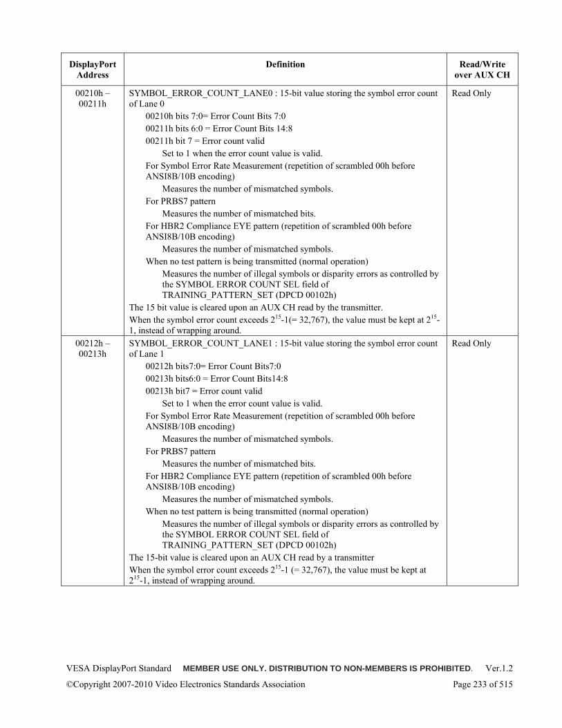
VESA DisplayPort Standard MEMBER USE ONLY. DISTRIBUTION TO NON-MEMBERS IS PROHIBITED. Ver.1.2
©Copyright 2007-2010 Video Electronics Standards Association Page 233 of 515
DisplayPort Address
Definition Read/Write over AUX CH
00210h – 00211h
SYMBOL_ERROR_COUNT_LANE0 : 15-bit value storing the symbol error count of Lane 0
00210h bits 7:0= Error Count Bits 7:0 00211h bits 6:0 = Error Count Bits 14:8 00211h bit 7 = Error count valid
Set to 1 when the error count value is valid. For Symbol Error Rate Measurement (repetition of scrambled 00h before ANSI8B/10B encoding)
Measures the number of mismatched symbols. For PRBS7 pattern
Measures the number of mismatched bits. For HBR2 Compliance EYE pattern (repetition of scrambled 00h before ANSI8B/10B encoding)
Measures the number of mismatched symbols. When no test pattern is being transmitted (normal operation)
Measures the number of illegal symbols or disparity errors as controlled by the SYMBOL ERROR COUNT SEL field of TRAINING_PATTERN_SET (DPCD 00102h)
The 15 bit value is cleared upon an AUX CH read by the transmitter. When the symbol error count exceeds 215-1(= 32,767), the value must be kept at 215-1, instead of wrapping around.
Read Only
00212h – 00213h
SYMBOL_ERROR_COUNT_LANE1 : 15-bit value storing the symbol error count of Lane 1
00212h bits7:0= Error Count Bits7:0 00213h bits6:0 = Error Count Bits14:8 00213h bit7 = Error count valid
Set to 1 when the error count value is valid. For Symbol Error Rate Measurement (repetition of scrambled 00h before ANSI8B/10B encoding)
Measures the number of mismatched symbols. For PRBS7 pattern
Measures the number of mismatched bits. For HBR2 Compliance EYE pattern (repetition of scrambled 00h before ANSI8B/10B encoding)
Measures the number of mismatched symbols. When no test pattern is being transmitted (normal operation)
Measures the number of illegal symbols or disparity errors as controlled by the SYMBOL ERROR COUNT SEL field of TRAINING_PATTERN_SET (DPCD 00102h)
The 15-bit value is cleared upon an AUX CH read by a transmitter When the symbol error count exceeds 215-1 (= 32,767), the value must be kept at 215-1, instead of wrapping around.
Read Only
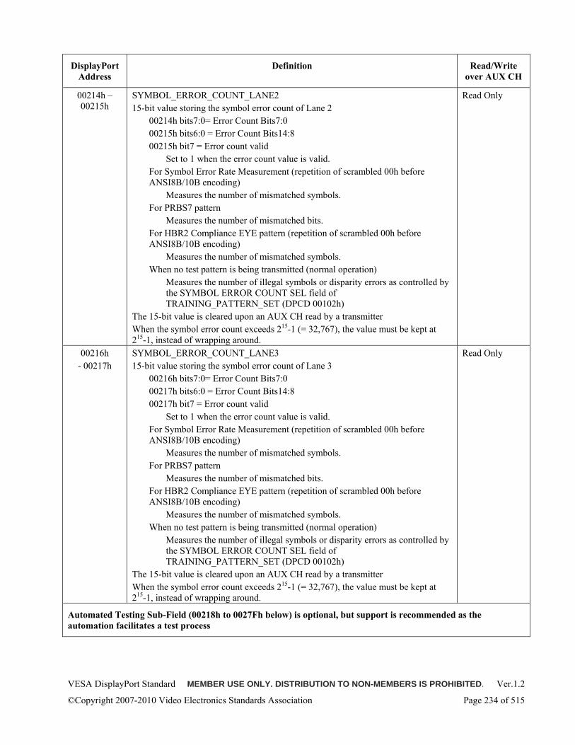
VESA DisplayPort Standard MEMBER USE ONLY. DISTRIBUTION TO NON-MEMBERS IS PROHIBITED. Ver.1.2
©Copyright 2007-2010 Video Electronics Standards Association Page 234 of 515
DisplayPort Address
Definition Read/Write over AUX CH
00214h – 00215h
SYMBOL_ERROR_COUNT_LANE2 15-bit value storing the symbol error count of Lane 2
00214h bits7:0= Error Count Bits7:0 00215h bits6:0 = Error Count Bits14:8 00215h bit7 = Error count valid
Set to 1 when the error count value is valid. For Symbol Error Rate Measurement (repetition of scrambled 00h before ANSI8B/10B encoding)
Measures the number of mismatched symbols. For PRBS7 pattern
Measures the number of mismatched bits. For HBR2 Compliance EYE pattern (repetition of scrambled 00h before ANSI8B/10B encoding)
Measures the number of mismatched symbols. When no test pattern is being transmitted (normal operation)
Measures the number of illegal symbols or disparity errors as controlled by the SYMBOL ERROR COUNT SEL field of TRAINING_PATTERN_SET (DPCD 00102h)
The 15-bit value is cleared upon an AUX CH read by a transmitter When the symbol error count exceeds 215-1 (= 32,767), the value must be kept at 215-1, instead of wrapping around.
Read Only
00216h - 00217h
SYMBOL_ERROR_COUNT_LANE3 15-bit value storing the symbol error count of Lane 3
00216h bits7:0= Error Count Bits7:0 00217h bits6:0 = Error Count Bits14:8 00217h bit7 = Error count valid
Set to 1 when the error count value is valid. For Symbol Error Rate Measurement (repetition of scrambled 00h before ANSI8B/10B encoding)
Measures the number of mismatched symbols. For PRBS7 pattern
Measures the number of mismatched bits. For HBR2 Compliance EYE pattern (repetition of scrambled 00h before ANSI8B/10B encoding)
Measures the number of mismatched symbols. When no test pattern is being transmitted (normal operation)
Measures the number of illegal symbols or disparity errors as controlled by the SYMBOL ERROR COUNT SEL field of TRAINING_PATTERN_SET (DPCD 00102h)
The 15-bit value is cleared upon an AUX CH read by a transmitter When the symbol error count exceeds 215-1 (= 32,767), the value must be kept at 215-1, instead of wrapping around.
Read Only
Automated Testing Sub-Field (00218h to 0027Fh below) is optional, but support is recommended as the automation facilitates a test process
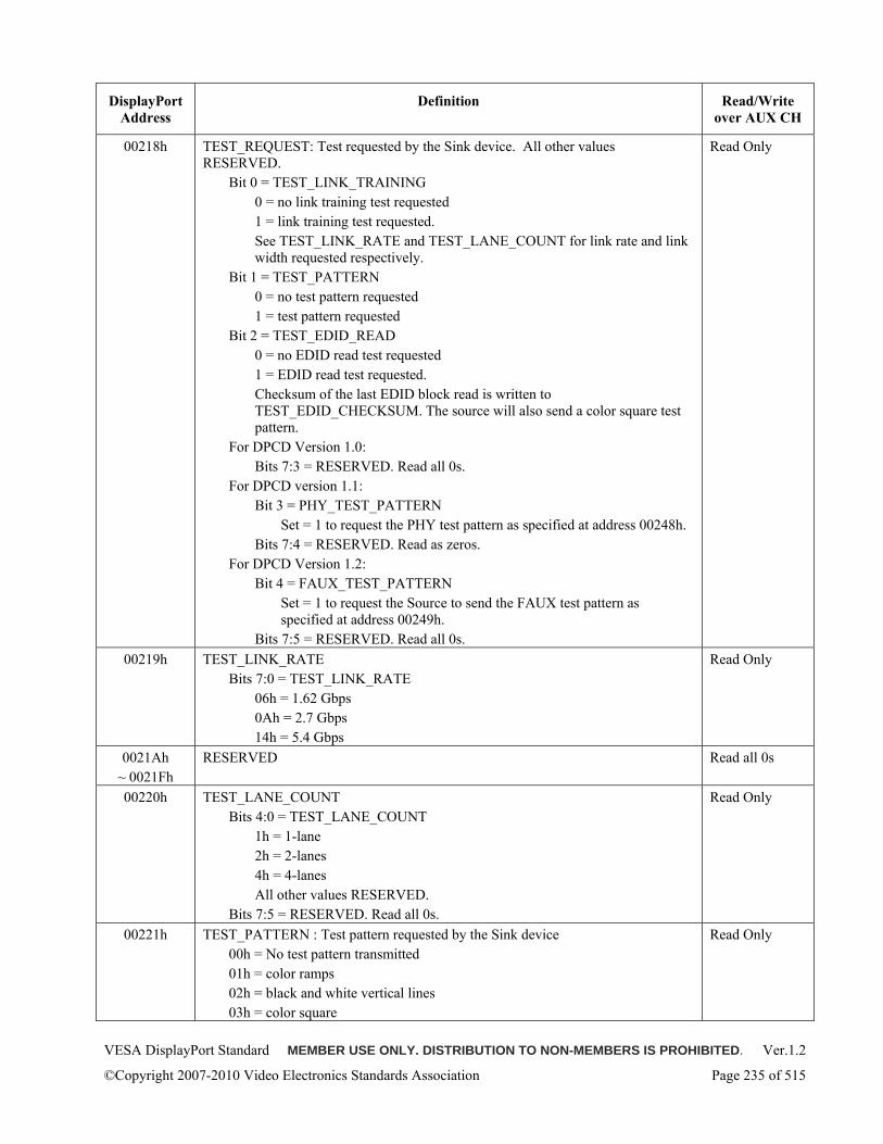
VESA DisplayPort Standard MEMBER USE ONLY. DISTRIBUTION TO NON-MEMBERS IS PROHIBITED. Ver.1.2
©Copyright 2007-2010 Video Electronics Standards Association Page 235 of 515
DisplayPort Address
Definition Read/Write over AUX CH
00218h TEST_REQUEST: Test requested by the Sink device. All other values RESERVED.
Bit 0 = TEST_LINK_TRAINING 0 = no link training test requested 1 = link training test requested. See TEST_LINK_RATE and TEST_LANE_COUNT for link rate and link width requested respectively.
Bit 1 = TEST_PATTERN 0 = no test pattern requested 1 = test pattern requested
Bit 2 = TEST_EDID_READ 0 = no EDID read test requested 1 = EDID read test requested. Checksum of the last EDID block read is written to TEST_EDID_CHECKSUM. The source will also send a color square test pattern.
For DPCD Version 1.0: Bits 7:3 = RESERVED. Read all 0s.
For DPCD version 1.1: Bit 3 = PHY_TEST_PATTERN
Set = 1 to request the PHY test pattern as specified at address 00248h. Bits 7:4 = RESERVED. Read as zeros.
For DPCD Version 1.2: Bit 4 = FAUX_TEST_PATTERN
Set = 1 to request the Source to send the FAUX test pattern as specified at address 00249h.
Bits 7:5 = RESERVED. Read all 0s.
Read Only
00219h TEST_LINK_RATE Bits 7:0 = TEST_LINK_RATE
06h = 1.62 Gbps 0Ah = 2.7 Gbps 14h = 5.4 Gbps
Read Only
0021Ah ~ 0021Fh
RESERVED Read all 0s
00220h TEST_LANE_COUNT Bits 4:0 = TEST_LANE_COUNT
1h = 1-lane 2h = 2-lanes 4h = 4-lanes All other values RESERVED.
Bits 7:5 = RESERVED. Read all 0s.
Read Only
00221h TEST_PATTERN : Test pattern requested by the Sink device 00h = No test pattern transmitted 01h = color ramps 02h = black and white vertical lines 03h = color square
Read Only
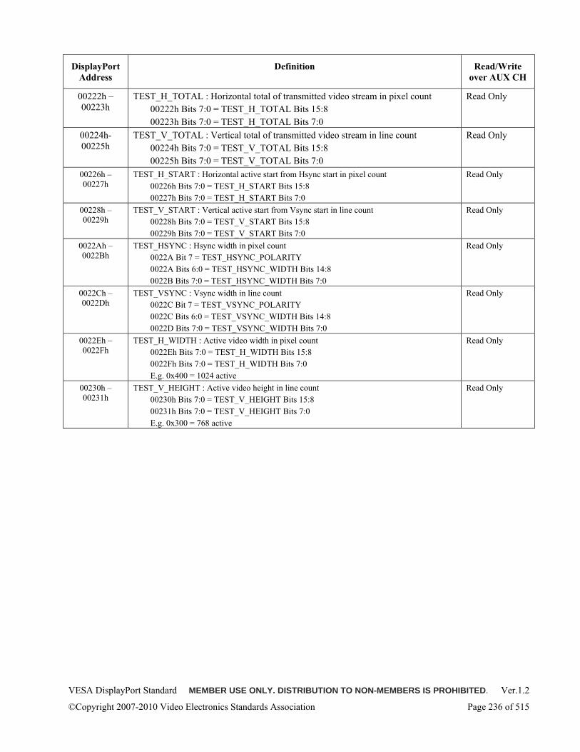
VESA DisplayPort Standard MEMBER USE ONLY. DISTRIBUTION TO NON-MEMBERS IS PROHIBITED. Ver.1.2
©Copyright 2007-2010 Video Electronics Standards Association Page 236 of 515
DisplayPort Address
Definition Read/Write over AUX CH
00222h – 00223h
TEST_H_TOTAL : Horizontal total of transmitted video stream in pixel count 00222h Bits 7:0 = TEST_H_TOTAL Bits 15:8 00223h Bits 7:0 = TEST_H_TOTAL Bits 7:0
Read Only
00224h- 00225h
TEST_V_TOTAL : Vertical total of transmitted video stream in line count 00224h Bits 7:0 = TEST_V_TOTAL Bits 15:8 00225h Bits 7:0 = TEST_V_TOTAL Bits 7:0
Read Only
00226h – 00227h
TEST_H_START : Horizontal active start from Hsync start in pixel count 00226h Bits 7:0 = TEST_H_START Bits 15:8 00227h Bits 7:0 = TEST_H_START Bits 7:0
Read Only
00228h – 00229h
TEST_V_START : Vertical active start from Vsync start in line count 00228h Bits 7:0 = TEST_V_START Bits 15:8 00229h Bits 7:0 = TEST_V_START Bits 7:0
Read Only
0022Ah – 0022Bh
TEST_HSYNC : Hsync width in pixel count 0022A Bit 7 = TEST_HSYNC_POLARITY 0022A Bits 6:0 = TEST_HSYNC_WIDTH Bits 14:8 0022B Bits 7:0 = TEST_HSYNC_WIDTH Bits 7:0
Read Only
0022Ch – 0022Dh
TEST_VSYNC : Vsync width in line count 0022C Bit 7 = TEST_VSYNC_POLARITY 0022C Bits 6:0 = TEST_VSYNC_WIDTH Bits 14:8 0022D Bits 7:0 = TEST_VSYNC_WIDTH Bits 7:0
Read Only
0022Eh – 0022Fh
TEST_H_WIDTH : Active video width in pixel count 0022Eh Bits 7:0 = TEST_H_WIDTH Bits 15:8 0022Fh Bits 7:0 = TEST_H_WIDTH Bits 7:0 E.g. 0x400 = 1024 active
Read Only
00230h – 00231h
TEST_V_HEIGHT : Active video height in line count 00230h Bits 7:0 = TEST_V_HEIGHT Bits 15:8 00231h Bits 7:0 = TEST_V_HEIGHT Bits 7:0 E.g. 0x300 = 768 active
Read Only
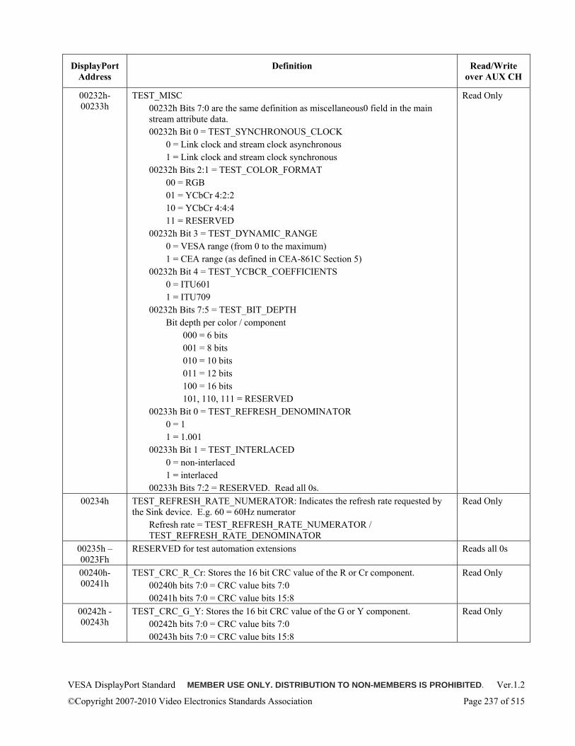
VESA DisplayPort Standard MEMBER USE ONLY. DISTRIBUTION TO NON-MEMBERS IS PROHIBITED. Ver.1.2
©Copyright 2007-2010 Video Electronics Standards Association Page 237 of 515
DisplayPort Address
Definition Read/Write over AUX CH
00232h- 00233h
TEST_MISC 00232h Bits 7:0 are the same definition as miscellaneous0 field in the main stream attribute data. 00232h Bit 0 = TEST_SYNCHRONOUS_CLOCK
0 = Link clock and stream clock asynchronous 1 = Link clock and stream clock synchronous
00232h Bits 2:1 = TEST_COLOR_FORMAT 00 = RGB 01 = YCbCr 4:2:2 10 = YCbCr 4:4:4 11 = RESERVED
00232h Bit 3 = TEST_DYNAMIC_RANGE 0 = VESA range (from 0 to the maximum) 1 = CEA range (as defined in CEA-861C Section 5)
00232h Bit 4 = TEST_YCBCR_COEFFICIENTS 0 = ITU601 1 = ITU709
00232h Bits 7:5 = TEST_BIT_DEPTH Bit depth per color / component
000 = 6 bits 001 = 8 bits 010 = 10 bits 011 = 12 bits 100 = 16 bits 101, 110, 111 = RESERVED
00233h Bit 0 = TEST_REFRESH_DENOMINATOR 0 = 1 1 = 1.001
00233h Bit 1 = TEST_INTERLACED 0 = non-interlaced 1 = interlaced
00233h Bits 7:2 = RESERVED. Read all 0s.
Read Only
00234h TEST_REFRESH_RATE_NUMERATOR: Indicates the refresh rate requested by the Sink device. E.g. 60 = 60Hz numerator
Refresh rate = TEST_REFRESH_RATE_NUMERATOR / TEST_REFRESH_RATE_DENOMINATOR
Read Only
00235h – 0023Fh
RESERVED for test automation extensions Reads all 0s
00240h-00241h
TEST_CRC_R_Cr: Stores the 16 bit CRC value of the R or Cr component. 00240h bits 7:0 = CRC value bits 7:0 00241h bits 7:0 = CRC value bits 15:8
Read Only
00242h -00243h
TEST_CRC_G_Y: Stores the 16 bit CRC value of the G or Y component. 00242h bits 7:0 = CRC value bits 7:0 00243h bits 7:0 = CRC value bits 15:8
Read Only
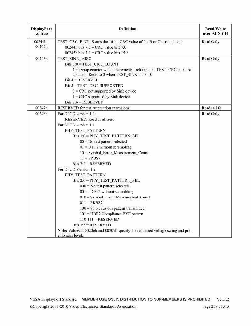
VESA DisplayPort Standard MEMBER USE ONLY. DISTRIBUTION TO NON-MEMBERS IS PROHIBITED. Ver.1.2
©Copyright 2007-2010 Video Electronics Standards Association Page 238 of 515
DisplayPort Address
Definition Read/Write over AUX CH
00244h -00245h
TEST_CRC_B_Cb: Stores the 16-bit CRC value of the B or Cb component. 00244h bits 7:0 = CRC value bits 7:0 00245h bits 7:0 = CRC value bits 15:8
Read Only
00246h TEST_SINK_MISC Bits 3:0 = TEST_CRC_COUNT
4 bit wrap counter which increments each time the TEST_CRC_x_x are updated. Reset to 0 when TEST_SINK bit 0 = 0.
Bit 4 = RESERVED Bit 5 = TEST_CRC_SUPPORTED
0 = CRC not supported by Sink device 1 = CRC supported by Sink device
Bits 7:6 = RESERVED
Read Only
00247h RESERVED for test automation extensions Reads all 0s 00248h For DPCD version 1.0:
RESERVED. Read as all zero. For DPCD version 1.1
PHY_TEST_PATTERN Bits 1:0 = PHY_TEST_PATTERN_SEL
00 = No test pattern selected 01 = D10.2 without scrambling 10 = Symbol_Error_Measurement_Count 11 = PRBS7
Bits 7:2 = RESERVED For DPCD Version 1.2
PHY_TEST_PATTERN Bits 2:0 = PHY_TEST_PATTERN_SEL
000 = No test pattern selected 001 = D10.2 without scrambling 010 = Symbol_Error_Measurement_Count 011 = PRBS7 100 = 80 bit custom pattern transmitted 101 = HBR2 Compliance EYE pattern 110-111 = RESERVED
Bits 7:3 = RESERVED Note: Values at 00206h and 00207h specify the requested voltage swing and pre-emphasis level.
Read Only
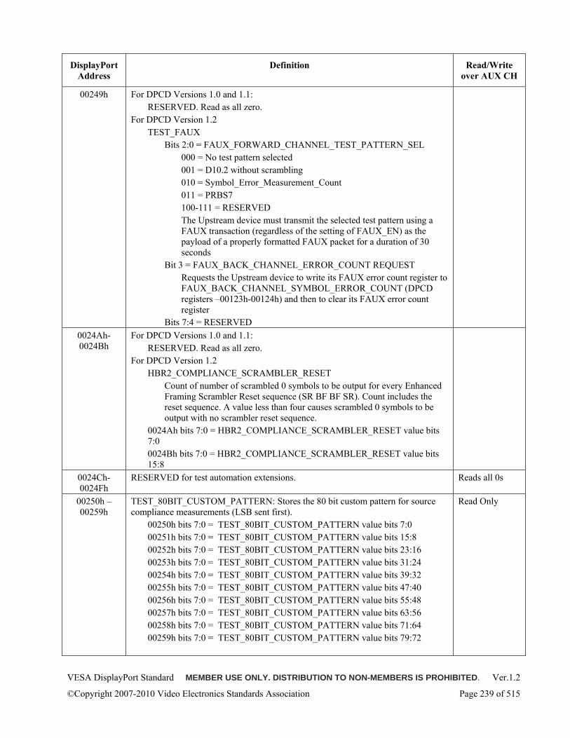
VESA DisplayPort Standard MEMBER USE ONLY. DISTRIBUTION TO NON-MEMBERS IS PROHIBITED. Ver.1.2
©Copyright 2007-2010 Video Electronics Standards Association Page 239 of 515
DisplayPort Address
Definition Read/Write over AUX CH
00249h For DPCD Versions 1.0 and 1.1: RESERVED. Read as all zero.
For DPCD Version 1.2 TEST_FAUX
Bits 2:0 = FAUX_FORWARD_CHANNEL_TEST_PATTERN_SEL 000 = No test pattern selected 001 = D10.2 without scrambling 010 = Symbol_Error_Measurement_Count 011 = PRBS7 100-111 = RESERVED The Upstream device must transmit the selected test pattern using a FAUX transaction (regardless of the setting of FAUX_EN) as the payload of a properly formatted FAUX packet for a duration of 30 seconds
Bit 3 = FAUX_BACK_CHANNEL_ERROR_COUNT REQUEST Requests the Upstream device to write its FAUX error count register to FAUX_BACK_CHANNEL_SYMBOL_ERROR_COUNT (DPCD registers –00123h-00124h) and then to clear its FAUX error count register
Bits 7:4 = RESERVED
0024Ah-0024Bh
For DPCD Versions 1.0 and 1.1: RESERVED. Read as all zero.
For DPCD Version 1.2 HBR2_COMPLIANCE_SCRAMBLER_RESET
Count of number of scrambled 0 symbols to be output for every Enhanced Framing Scrambler Reset sequence (SR BF BF SR). Count includes the reset sequence. A value less than four causes scrambled 0 symbols to be output with no scrambler reset sequence.
0024Ah bits 7:0 = HBR2_COMPLIANCE_SCRAMBLER_RESET value bits 7:0 0024Bh bits 7:0 = HBR2_COMPLIANCE_SCRAMBLER_RESET value bits 15:8
0024Ch-0024Fh
RESERVED for test automation extensions. Reads all 0s
00250h – 00259h
TEST_80BIT_CUSTOM_PATTERN: Stores the 80 bit custom pattern for source compliance measurements (LSB sent first).
00250h bits 7:0 = TEST_80BIT_CUSTOM_PATTERN value bits 7:0 00251h bits 7:0 = TEST_80BIT_CUSTOM_PATTERN value bits 15:8 00252h bits 7:0 = TEST_80BIT_CUSTOM_PATTERN value bits 23:16 00253h bits 7:0 = TEST_80BIT_CUSTOM_PATTERN value bits 31:24 00254h bits 7:0 = TEST_80BIT_CUSTOM_PATTERN value bits 39:32 00255h bits 7:0 = TEST_80BIT_CUSTOM_PATTERN value bits 47:40 00256h bits 7:0 = TEST_80BIT_CUSTOM_PATTERN value bits 55:48 00257h bits 7:0 = TEST_80BIT_CUSTOM_PATTERN value bits 63:56 00258h bits 7:0 = TEST_80BIT_CUSTOM_PATTERN value bits 71:64 00259h bits 7:0 = TEST_80BIT_CUSTOM_PATTERN value bits 79:72
Read Only
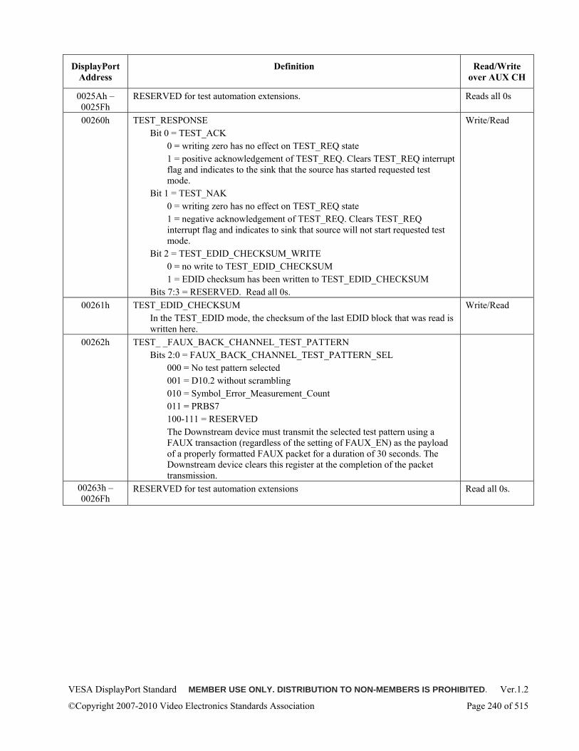
VESA DisplayPort Standard MEMBER USE ONLY. DISTRIBUTION TO NON-MEMBERS IS PROHIBITED. Ver.1.2
©Copyright 2007-2010 Video Electronics Standards Association Page 240 of 515
DisplayPort Address
Definition Read/Write over AUX CH
0025Ah – 0025Fh
RESERVED for test automation extensions. Reads all 0s
00260h TEST_RESPONSE Bit 0 = TEST_ACK
0 = writing zero has no effect on TEST_REQ state 1 = positive acknowledgement of TEST_REQ. Clears TEST_REQ interrupt flag and indicates to the sink that the source has started requested test mode.
Bit 1 = TEST_NAK 0 = writing zero has no effect on TEST_REQ state 1 = negative acknowledgement of TEST_REQ. Clears TEST_REQ interrupt flag and indicates to sink that source will not start requested test mode.
Bit 2 = TEST_EDID_CHECKSUM_WRITE 0 = no write to TEST_EDID_CHECKSUM 1 = EDID checksum has been written to TEST_EDID_CHECKSUM
Bits 7:3 = RESERVED. Read all 0s.
Write/Read
00261h TEST_EDID_CHECKSUM In the TEST_EDID mode, the checksum of the last EDID block that was read is written here.
Write/Read
00262h TEST_ _FAUX_BACK_CHANNEL_TEST_PATTERN Bits 2:0 = FAUX_BACK_CHANNEL_TEST_PATTERN_SEL
000 = No test pattern selected 001 = D10.2 without scrambling 010 = Symbol_Error_Measurement_Count 011 = PRBS7 100-111 = RESERVED The Downstream device must transmit the selected test pattern using a FAUX transaction (regardless of the setting of FAUX_EN) as the payload of a properly formatted FAUX packet for a duration of 30 seconds. The Downstream device clears this register at the completion of the packet transmission.
00263h – 0026Fh
RESERVED for test automation extensions Read all 0s.
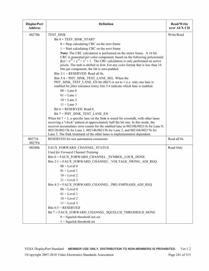
VESA DisplayPort Standard MEMBER USE ONLY. DISTRIBUTION TO NON-MEMBERS IS PROHIBITED. Ver.1.2
©Copyright 2007-2010 Video Electronics Standards Association Page 241 of 515
DisplayPort Address
Definition Read/Write over AUX CH
00270h TEST_SINK Bit 0 = TEST_SINK_START
0 = Stop calculating CRC on the next frame 1 = Start calculating CRC on the next frame Note: The CRC calculation is performed on the entire frame. A 16 bit CRC is generated per color component, based on the following polynomial: f(x) = x16 + x15 + x2 + 1. The CRC calculation is only performed on active pixels. The msb is shifted in first. For any color format that is less than 16 bits per component, the lsb is zero-padded.
Bits 3:1 = RESERVED. Read all 0s. Bits 5:4 = PHY_SINK_TEST_LANE_SEL. When the PHY_SINK_TEST_LANE_EN bit (Bit7) is set to 1 (i.e. only one lane is enabled for jitter tolerance tests), bits 5:4 indicate which lane is enabled.
00 = Lane 0 01 = Lane 1 10 = Lane 2 11 = Lane 3
Bit 6 = RESERVED. Read 0. Bit 7 = PHY_SINK_TEST_LANE_EN
When bit 7 = 1, a specific lane on the Sink is tested for crosstalk, with other lanes receiving a "clock" pattern at approximately half the bit rate. In this mode, the receiver accumulates error counts for the enabled lane in 00210h/00211h for Lane 0, 00212h/00213h for Lane 1, 00214h/00215h for Lane 2, and 00216h/00217h for Lane 3. The Sink treatment of the other lanes is implementation dependent.
Write/Read
00271h – 0027Fh
RESERVED for test automation extensions Read all 0s.
00280h FAUX_FORWARD_CHANNEL_STATUS Used for Forward Channel Training Bits 0 = FAUX_FORWARD_CHANNEL _SYMBOL_LOCK_DONE Bits 2:1 = FAUX_FORWARD_CHANNEL _VOLTAGE_SWING_ADJ_REQ
00 = Level 0 01 = Level 1 10 = Level 2 11 = Level 3
Bits 4:3 = FAUX_FORWARD_CHANNEL _PRE-EMPHASIS_ADJ_REQ 00 = Level 0 01 = Level 1 10 = Level 2 11 = Level 3
Bits 6:5 = RESERVED Bit 7 = FAUX_FORWARD_CHANNEL_SQUELCH_THRESHOLD_DONE
0 = Squelch threshold not set 1 = Squelch threshold set
Read Only
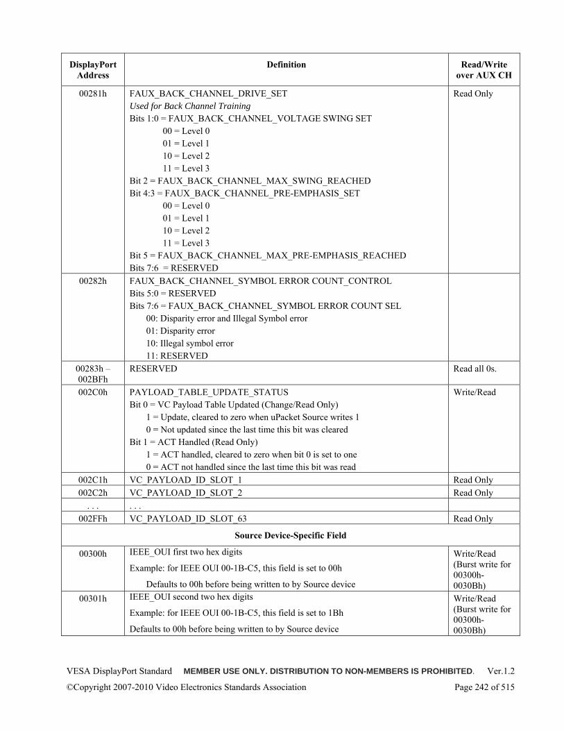
VESA DisplayPort Standard MEMBER USE ONLY. DISTRIBUTION TO NON-MEMBERS IS PROHIBITED. Ver.1.2
©Copyright 2007-2010 Video Electronics Standards Association Page 242 of 515
DisplayPort Address
Definition Read/Write over AUX CH
00281h FAUX_BACK_CHANNEL_DRIVE_SET Used for Back Channel Training Bits 1:0 = FAUX_BACK_CHANNEL_VOLTAGE SWING SET
00 = Level 0 01 = Level 1 10 = Level 2 11 = Level 3
Bit 2 = FAUX_BACK_CHANNEL_MAX_SWING_REACHED Bit 4:3 = FAUX_BACK_CHANNEL_PRE-EMPHASIS_SET
00 = Level 0 01 = Level 1 10 = Level 2 11 = Level 3
Bit 5 = FAUX_BACK_CHANNEL_MAX_PRE-EMPHASIS_REACHED Bits 7:6 = RESERVED
Read Only
00282h FAUX_BACK_CHANNEL_SYMBOL ERROR COUNT_CONTROL Bits 5:0 = RESERVED Bits 7:6 = FAUX_BACK_CHANNEL_SYMBOL ERROR COUNT SEL
00: Disparity error and Illegal Symbol error 01: Disparity error 10: Illegal symbol error 11: RESERVED
00283h – 002BFh
RESERVED Read all 0s.
002C0h PAYLOAD_TABLE_UPDATE_STATUS Bit 0 = VC Payload Table Updated (Change/Read Only)
1 = Update, cleared to zero when uPacket Source writes 1 0 = Not updated since the last time this bit was cleared
Bit 1 = ACT Handled (Read Only) 1 = ACT handled, cleared to zero when bit 0 is set to one 0 = ACT not handled since the last time this bit was read
Write/Read
002C1h VC_PAYLOAD_ID_SLOT_1 Read Only 002C2h VC_PAYLOAD_ID_SLOT_2 Read Only
. . . . . . 002FFh VC_PAYLOAD_ID_SLOT_63 Read Only
Source Device-Specific Field
00300h IEEE_OUI first two hex digits
Example: for IEEE OUI 00-1B-C5, this field is set to 00h
Defaults to 00h before being written to by Source device
Write/Read (Burst write for 00300h-0030Bh)
00301h IEEE_OUI second two hex digits
Example: for IEEE OUI 00-1B-C5, this field is set to 1Bh
Defaults to 00h before being written to by Source device
Write/Read (Burst write for 00300h-0030Bh)
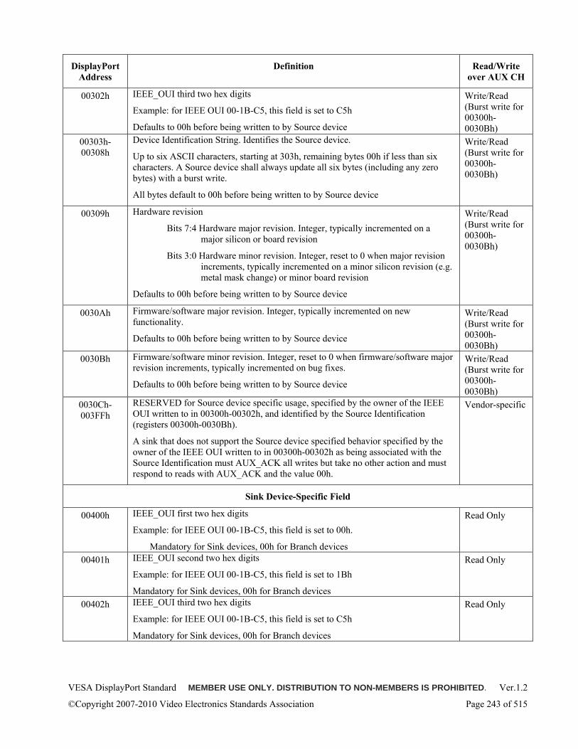
VESA DisplayPort Standard MEMBER USE ONLY. DISTRIBUTION TO NON-MEMBERS IS PROHIBITED. Ver.1.2
©Copyright 2007-2010 Video Electronics Standards Association Page 243 of 515
DisplayPort Address
Definition Read/Write over AUX CH
00302h IEEE_OUI third two hex digits
Example: for IEEE OUI 00-1B-C5, this field is set to C5h
Defaults to 00h before being written to by Source device
Write/Read (Burst write for 00300h-0030Bh)
00303h-00308h
Device Identification String. Identifies the Source device.
Up to six ASCII characters, starting at 303h, remaining bytes 00h if less than six characters. A Source device shall always update all six bytes (including any zero bytes) with a burst write.
All bytes default to 00h before being written to by Source device
Write/Read (Burst write for 00300h-0030Bh)
00309h Hardware revision
Bits 7:4 Hardware major revision. Integer, typically incremented on a major silicon or board revision
Bits 3:0 Hardware minor revision. Integer, reset to 0 when major revision increments, typically incremented on a minor silicon revision (e.g. metal mask change) or minor board revision
Defaults to 00h before being written to by Source device
Write/Read (Burst write for 00300h-0030Bh)
0030Ah Firmware/software major revision. Integer, typically incremented on new functionality.
Defaults to 00h before being written to by Source device
Write/Read (Burst write for 00300h-0030Bh)
0030Bh Firmware/software minor revision. Integer, reset to 0 when firmware/software major revision increments, typically incremented on bug fixes.
Defaults to 00h before being written to by Source device
Write/Read (Burst write for 00300h-0030Bh)
0030Ch-003FFh
RESERVED for Source device specific usage, specified by the owner of the IEEE OUI written to in 00300h-00302h, and identified by the Source Identification (registers 00300h-0030Bh).
A sink that does not support the Source device specified behavior specified by the owner of the IEEE OUI written to in 00300h-00302h as being associated with the Source Identification must AUX_ACK all writes but take no other action and must respond to reads with AUX_ACK and the value 00h.
Vendor-specific
Sink Device-Specific Field
00400h IEEE_OUI first two hex digits
Example: for IEEE OUI 00-1B-C5, this field is set to 00h.
Mandatory for Sink devices, 00h for Branch devices
Read Only
00401h IEEE_OUI second two hex digits
Example: for IEEE OUI 00-1B-C5, this field is set to 1Bh
Mandatory for Sink devices, 00h for Branch devices
Read Only
00402h IEEE_OUI third two hex digits
Example: for IEEE OUI 00-1B-C5, this field is set to C5h
Mandatory for Sink devices, 00h for Branch devices
Read Only
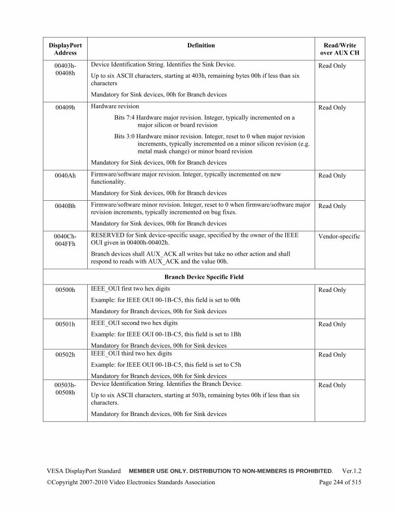
VESA DisplayPort Standard MEMBER USE ONLY. DISTRIBUTION TO NON-MEMBERS IS PROHIBITED. Ver.1.2
©Copyright 2007-2010 Video Electronics Standards Association Page 244 of 515
DisplayPort Address
Definition Read/Write over AUX CH
00403h-00408h
Device Identification String. Identifies the Sink Device.
Up to six ASCII characters, starting at 403h, remaining bytes 00h if less than six characters
Mandatory for Sink devices, 00h for Branch devices
Read Only
00409h Hardware revision
Bits 7:4 Hardware major revision. Integer, typically incremented on a major silicon or board revision
Bits 3:0 Hardware minor revision. Integer, reset to 0 when major revision increments, typically incremented on a minor silicon revision (e.g. metal mask change) or minor board revision
Mandatory for Sink devices, 00h for Branch devices
Read Only
0040Ah Firmware/software major revision. Integer, typically incremented on new functionality.
Mandatory for Sink devices, 00h for Branch devices
Read Only
0040Bh Firmware/software minor revision. Integer, reset to 0 when firmware/software major revision increments, typically incremented on bug fixes.
Mandatory for Sink devices, 00h for Branch devices
Read Only
0040Ch-004FFh
RESERVED for Sink device-specific usage, specified by the owner of the IEEE OUI given in 00400h-00402h.
Branch devices shall AUX_ACK all writes but take no other action and shall respond to reads with AUX_ACK and the value 00h.
Vendor-specific
Branch Device Specific Field
00500h IEEE_OUI first two hex digits
Example: for IEEE OUI 00-1B-C5, this field is set to 00h
Mandatory for Branch devices, 00h for Sink devices
Read Only
00501h IEEE_OUI second two hex digits
Example: for IEEE OUI 00-1B-C5, this field is set to 1Bh
Mandatory for Branch devices, 00h for Sink devices
Read Only
00502h IEEE_OUI third two hex digits
Example: for IEEE OUI 00-1B-C5, this field is set to C5h
Mandatory for Branch devices, 00h for Sink devices
Read Only
00503h-00508h
Device Identification String. Identifies the Branch Device.
Up to six ASCII characters, starting at 503h, remaining bytes 00h if less than six characters.
Mandatory for Branch devices, 00h for Sink devices
Read Only
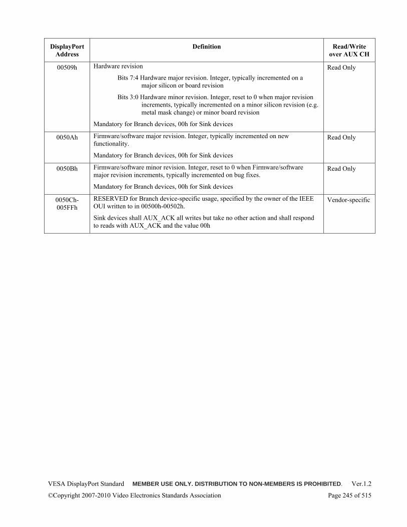
VESA DisplayPort Standard MEMBER USE ONLY. DISTRIBUTION TO NON-MEMBERS IS PROHIBITED. Ver.1.2
©Copyright 2007-2010 Video Electronics Standards Association Page 245 of 515
DisplayPort Address
Definition Read/Write over AUX CH
00509h Hardware revision
Bits 7:4 Hardware major revision. Integer, typically incremented on a major silicon or board revision
Bits 3:0 Hardware minor revision. Integer, reset to 0 when major revision increments, typically incremented on a minor silicon revision (e.g. metal mask change) or minor board revision
Mandatory for Branch devices, 00h for Sink devices
Read Only
0050Ah Firmware/software major revision. Integer, typically incremented on new functionality.
Mandatory for Branch devices, 00h for Sink devices
Read Only
0050Bh Firmware/software minor revision. Integer, reset to 0 when Firmware/software major revision increments, typically incremented on bug fixes.
Mandatory for Branch devices, 00h for Sink devices
Read Only
0050Ch-005FFh
RESERVED for Branch device-specific usage, specified by the owner of the IEEE OUI written to in 00500h-00502h.
Sink devices shall AUX_ACK all writes but take no other action and shall respond to reads with AUX_ACK and the value 00h
Vendor-specific
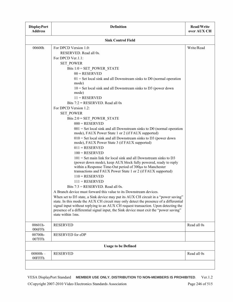
VESA DisplayPort Standard MEMBER USE ONLY. DISTRIBUTION TO NON-MEMBERS IS PROHIBITED. Ver.1.2
©Copyright 2007-2010 Video Electronics Standards Association Page 246 of 515
DisplayPort Address
Definition Read/Write over AUX CH
Sink Control Field
00600h For DPCD Version 1.0: RESERVED. Read all 0s.
For DPCD Ver.1.1: SET_POWER
Bits 1:0 = SET_POWER_STATE 00 = RESERVED 01 = Set local sink and all Downstream sinks to D0 (normal operation mode) 10 = Set local sink and all Downstream sinks to D3 (power down mode) 11 = RESERVED
Bits 7:2 = RESERVED. Read all 0s For DPCD Version 1.2:
SET_POWER Bits 2:0 = SET_POWER_STATE
000 = RESERVED 001 = Set local sink and all Downstream sinks to D0 (normal operation mode), FAUX Power State 1 or 2 (if FAUX supported) 010 = Set local sink and all Downstream sinks to D3 (power down mode), FAUX Power State 3 (if FAUX supported) 011 = RESERVED 100 = RESERVED 101 = Set main link for local sink and all Downstream sinks to D3 (power down mode), keep AUX block fully powered, ready to reply within a Response Time-Out period of 300μs to Manchester transactions and FAUX Power State 1 or 2 (if FAUX supported) 110 = RESERVED 111 = RESERVED
Bits 7:3 = RESERVED. Read all 0s. A Branch device must forward this value to its Downstream devices. When set to D3 state, a Sink device may put its AUX CH circuit in a “power saving” state. In this mode the AUX CH circuit may only detect the presence of a differential signal input without replying to an AUX CH request transaction. Upon detecting the presence of a differential signal input, the Sink device must exit the “power saving” state within 1ms.
Write/Read
00601h- 006FFh
RESERVED Read all 0s
00700h-007FFh
RESERVED for eDP
Usage to be Defined
00800h – 00FFFh
RESERVED Read all 0s
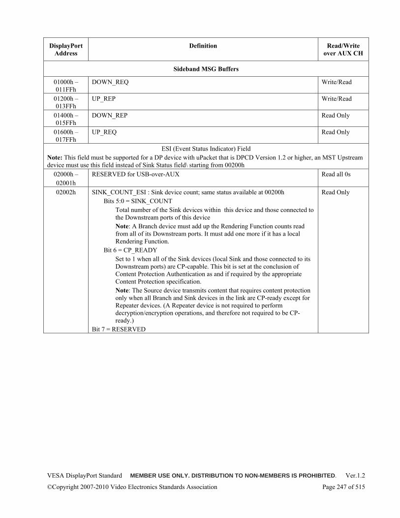
VESA DisplayPort Standard MEMBER USE ONLY. DISTRIBUTION TO NON-MEMBERS IS PROHIBITED. Ver.1.2
©Copyright 2007-2010 Video Electronics Standards Association Page 247 of 515
DisplayPort Address
Definition Read/Write over AUX CH
Sideband MSG Buffers
01000h – 011FFh
DOWN_REQ Write/Read
01200h – 013FFh
UP_REP Write/Read
01400h – 015FFh
DOWN_REP Read Only
01600h – 017FFh
UP_REQ Read Only
ESI (Event Status Indicator) Field Note: This field must be supported for a DP device with uPacket that is DPCD Version 1.2 or higher, an MST Upstream device must use this field instead of Sink Status field\ starting from 00200h
02000h – 02001h
RESERVED for USB-over-AUX Read all 0s
02002h SINK_COUNT_ESI : Sink device count; same status available at 00200h Bits 5:0 = SINK_COUNT
Total number of the Sink devices within this device and those connected to the Downstream ports of this device Note: A Branch device must add up the Rendering Function counts read from all of its Downstream ports. It must add one more if it has a local Rendering Function.
Bit 6 = CP_READY Set to 1 when all of the Sink devices (local Sink and those connected to its Downstream ports) are CP-capable. This bit is set at the conclusion of Content Protection Authentication as and if required by the appropriate Content Protection specification. Note: The Source device transmits content that requires content protection only when all Branch and Sink devices in the link are CP-ready except for Repeater devices. (A Repeater device is not required to perform decryption/encryption operations, and therefore not required to be CP-ready.)
Bit 7 = RESERVED
Read Only
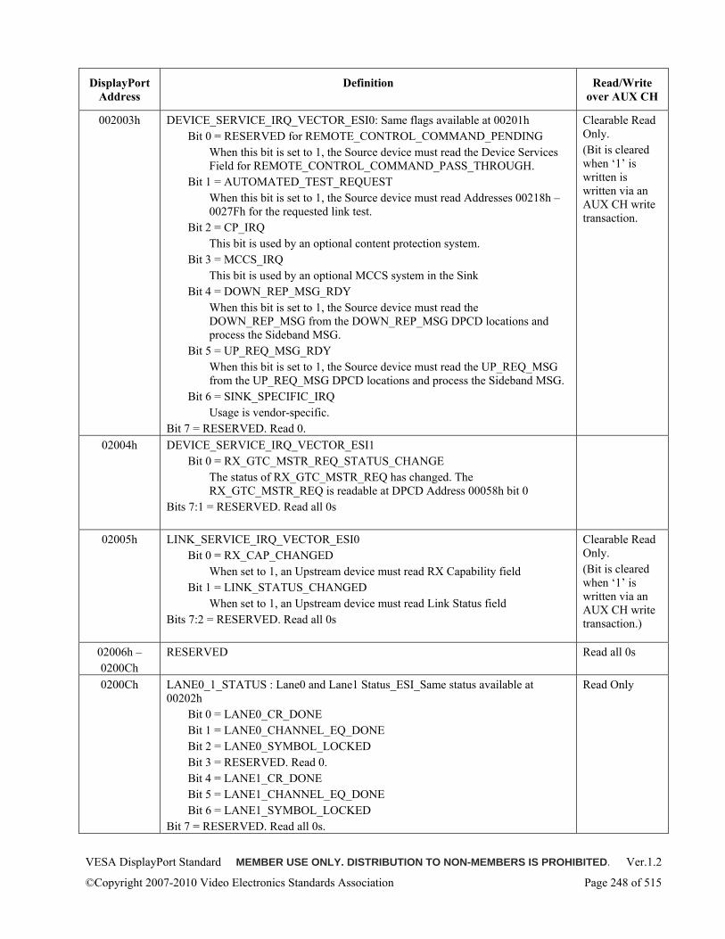
VESA DisplayPort Standard MEMBER USE ONLY. DISTRIBUTION TO NON-MEMBERS IS PROHIBITED. Ver.1.2
©Copyright 2007-2010 Video Electronics Standards Association Page 248 of 515
DisplayPort Address
Definition Read/Write over AUX CH
002003h DEVICE_SERVICE_IRQ_VECTOR_ESI0: Same flags available at 00201h Bit 0 = RESERVED for REMOTE_CONTROL_COMMAND_PENDING
When this bit is set to 1, the Source device must read the Device Services Field for REMOTE_CONTROL_COMMAND_PASS_THROUGH.
Bit 1 = AUTOMATED_TEST_REQUEST When this bit is set to 1, the Source device must read Addresses 00218h – 0027Fh for the requested link test.
Bit 2 = CP_IRQ This bit is used by an optional content protection system.
Bit 3 = MCCS_IRQ This bit is used by an optional MCCS system in the Sink
Bit 4 = DOWN_REP_MSG_RDY When this bit is set to 1, the Source device must read the DOWN_REP_MSG from the DOWN_REP_MSG DPCD locations and process the Sideband MSG.
Bit 5 = UP_REQ_MSG_RDY When this bit is set to 1, the Source device must read the UP_REQ_MSG from the UP_REQ_MSG DPCD locations and process the Sideband MSG.
Bit 6 = SINK_SPECIFIC_IRQ Usage is vendor-specific.
Bit 7 = RESERVED. Read 0.
Clearable Read Only. (Bit is cleared when ‘1’ is written is written via an AUX CH write transaction.
02004h DEVICE_SERVICE_IRQ_VECTOR_ESI1 Bit 0 = RX_GTC_MSTR_REQ_STATUS_CHANGE
The status of RX_GTC_MSTR_REQ has changed. The RX_GTC_MSTR_REQ is readable at DPCD Address 00058h bit 0
Bits 7:1 = RESERVED. Read all 0s
02005h LINK_SERVICE_IRQ_VECTOR_ESI0 Bit 0 = RX_CAP_CHANGED
When set to 1, an Upstream device must read RX Capability field Bit 1 = LINK_STATUS_CHANGED
When set to 1, an Upstream device must read Link Status field Bits 7:2 = RESERVED. Read all 0s
Clearable Read Only. (Bit is cleared when ‘1’ is written via an AUX CH write transaction.)
02006h – 0200Ch
RESERVED Read all 0s
0200Ch LANE0_1_STATUS : Lane0 and Lane1 Status_ESI_Same status available at 00202h
Bit 0 = LANE0_CR_DONE Bit 1 = LANE0_CHANNEL_EQ_DONE Bit 2 = LANE0_SYMBOL_LOCKED Bit 3 = RESERVED. Read 0. Bit 4 = LANE1_CR_DONE Bit 5 = LANE1_CHANNEL_EQ_DONE Bit 6 = LANE1_SYMBOL_LOCKED
Bit 7 = RESERVED. Read all 0s.
Read Only
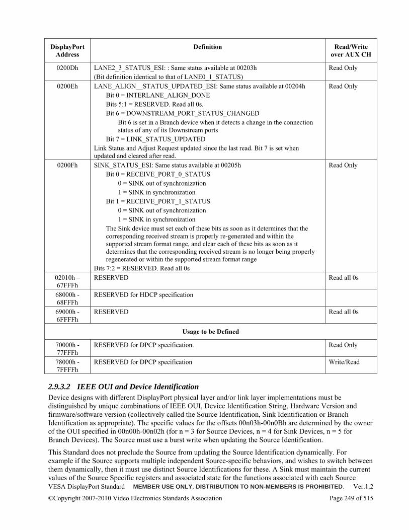
VESA DisplayPort Standard MEMBER USE ONLY. DISTRIBUTION TO NON-MEMBERS IS PROHIBITED. Ver.1.2
©Copyright 2007-2010 Video Electronics Standards Association Page 249 of 515
DisplayPort Address
Definition Read/Write over AUX CH
0200Dh LANE2_3_STATUS_ESI: : Same status available at 00203h (Bit definition identical to that of LANE0_1_STATUS)
Read Only
0200Eh LANE_ALIGN__STATUS_UPDATED_ESI: Same status available at 00204h Bit 0 = INTERLANE_ALIGN_DONE Bits 5:1 = RESERVED. Read all 0s. Bit 6 = DOWNSTREAM_PORT_STATUS_CHANGED
Bit 6 is set in a Branch device when it detects a change in the connection status of any of its Downstream ports
Bit 7 = LINK_STATUS_UPDATED Link Status and Adjust Request updated since the last read. Bit 7 is set when updated and cleared after read.
Read Only
0200Fh SINK_STATUS_ESI: Same status available at 00205h Bit 0 = RECEIVE_PORT_0_STATUS
0 = SINK out of synchronization 1 = SINK in synchronization
Bit 1 = RECEIVE_PORT_1_STATUS 0 = SINK out of synchronization 1 = SINK in synchronization
The Sink device must set each of these bits as soon as it determines that the corresponding received stream is properly re-generated and within the supported stream format range, and clear each of these bits as soon as it determines that the corresponding received stream is no longer being properly regenerated or within the supported stream format range
Bits 7:2 = RESERVED. Read all 0s
Read Only
02010h – 67FFFh
RESERVED Read all 0s
68000h - 68FFFh
RESERVED for HDCP specification
69000h - 6FFFFh
RESERVED Read all 0s
Usage to be Defined
70000h - 77FFFh
RESERVED for DPCP specification. Read Only
78000h - 7FFFFh
RESERVED for DPCP specification Write/Read
2.9.3.2 IEEE OUI and Device Identification Device designs with different DisplayPort physical layer and/or link layer implementations must be distinguished by unique combinations of IEEE OUI, Device Identification String, Hardware Version and firmware/software version (collectively called the Source Identification, Sink Identification or Branch Identification as appropriate). The specific values for the offsets 00n03h-00n0Bh are determined by the owner of the OUI specified in 00n00h-00n02h (for n = 3 for Source Devices, n = 4 for Sink Devices, n = 5 for Branch Devices). The Source must use a burst write when updating the Source Identification.
This Standard does not preclude the Source from updating the Source Identification dynamically. For example if the Source supports multiple independent Source-specific behaviors, and wishes to switch between them dynamically, then it must use distinct Source Identifications for these. A Sink must maintain the current values of the Source Specific registers and associated state for the functions associated with each Source
VESA DisplayPort Standard MEMBER USE ONLY. DISTRIBUTION TO NON-MEMBERS IS PROHIBITED. Ver.1.2
©Copyright 2007-2010 Video Electronics Standards Association Page 250 of 515
Identification that it supports, preserving these when the Source switches away from the corresponding Source Identification and reinstating them when the Source switches back to the corresponding Source Identification.
2.9.3.3 DPCD in Multi-Link Topology with SST-mode-only Source Device DisplayPort link has multiple links when one or more Sink devices connect to a Source device via Branch device(s). A Branch device forwarding SST transport format from an input port to an output port, acting as an SST-mode Repeater device, must comprehend the DPCD(s) of its Downstream links. An SST-only mode Upstream DisplayPort device must check only the DPCD of its immediate Downstream device regardless of the link topology.
For behavior of a Branch device upon detecting status change of Downstream ports, refer to Section 5.3.2.1.
2.9.3.3.1 Receiver Capability of Downstream Legacy Link Generally speaking, a legacy link does not have a link capability field equivalent to that defined for DPCD.
Capabilities vary: Some legacy links can support both audio and video, while others are limited to video only. Supported pixel data rate and color format are also dependent on the type of legacy link and its implementation.
A DisplayPort Source device, when connected to a legacy Sink device via a DisplayPort-to-legacy converter, must determine the stream format based on the Sink device capability expressed in the EDID of the legacy Sink device and whether the cable adaptor is an HDMI cable adaptor or not.
2.9.3.4 Link Initialization Through Link Training DisplayPort link initialization (before transporting a stream) must be performed unless the Source Main Link transmitter and the Sink Main Link receiver are already in synchronization as indicated in the Link Status field. During link initialization AUX CH services must be used to train the link with a desired set of link configuration parameters. For a detailed description of the Link Training sequence, refer to Section 3.5.1.2.
An exception for Link Training requirement exists for embedded DisplayPort connections. When DisplayPort Source device reads 1 in NO_AUX_HANDSHAKE_LINK_TRAINING bit of DPCD (Bit 6 of Address 3h) of DisplayPort Sink device, it may transmit Link Training Pattern 1 (which is a repetition of D10.2 symbols without scrambling) and Link Training Pattern 2 before switching to the normal operation without a handshake over the AUX CH (i.e. no AUX transactions are used to initiate training, during training or on completion of successful training).
There is another exception for a box-to-box connection. When DisplayPort Source device is resuming the transmission (e.g. after waking from sleep), the Source device may skip the AUX CH handshake for the link training if the following conditions are met:
• The Source device has determined that the HPD signal has remained asserted continuously (apart from HPD_IRQ notifications) since the link was last in full operation.
• The Source device has read 1 in NO_AUX_HANDSHAKE_LINK_TRAINING bit of DPCD (Bit 6 of Address 3h) after the initial Sink device detection.
If above conditions are met, and if the Source device determines that bandwidth to be used is the same as that used when the link was last in full operation, the Source device may transmit Link Training Pattern 1 and Link Training Pattern 2 (500us minimum for each) using the last known good voltage swing and pre-emphasis settings before switching to the normal operation without a handshake over the AUX CH. Whether the full Link Training is skipped or not, the DisplayPort Sink device must send an IRQ_HPD pulse over the HPD signal line when it fails to synchronize to the incoming Main Link stream.
After Link Training is successfully completed (which means DisplayPort receiver is synchronized to incoming Main Link data) and before transport of a main video stream starts, the Source Main Link
VESA DisplayPort Standard MEMBER USE ONLY. DISTRIBUTION TO NON-MEMBERS IS PROHIBITED. Ver.1.2
©Copyright 2007-2010 Video Electronics Standards Association Page 251 of 515
transmitter must be sending the “idle pattern” consisting of BS symbol set (BS symbol followed by VB-ID with its NoVideoStream_Flag set to 1 (Basic Framing) or BS+BF+BF+BS (Enhanced Framing)) inserted every 213 (or 8,192) link symbols. Every 512'th occurrence of the BS symbol set must be replaced by the corresponding scrambler reset symbol set (SR (Basic Framing) or SR+BF+BF+SR (Enhanced Framing)).
The Source device must start sending the idle pattern after it has cleared the Training_Pattern byte in the DPCD. The Sink device, should be ready to receive the “idle pattern” as soon as it updates the link status field of the DPCD to indicate the successful completion of Link Training to the Source device.
Link training may result in the available bandwidth being lower than that originally attempted (for example, an attempt to train at HBR fails, and training falls back to RBR). The Source device must not attempt to transmit an AV stream that requires a bandwidth higher than that actually in use.
A link may be retrained for some reason. A Source must be tolerant to the available bandwidth resulting from retraining being lower than the bandwidth resulting from prior training, and this may in turn require a video mode set change.
For a closed embedded connection, the DisplayPort transmitter and receiver may be set to pre-calibrated parameters without going through the full link training sequence. In this mode, the DisplayPort transmitter may start a normal operation following transmission of the Clock Recovery Pattern with pre-calibrated drive current and pre-emphasis level.
When switching to an MST transport format following the link training, the uPacket TX of an Upstream device must set MST_EN bit in DPCD prior to starting Link Training. The Upstream device is required to send a minimum of 4 MST Link Frames (4 SR cycles) of empty MTPs prior to startup of a stream.
2.9.3.5 Link Maintenance The Sink device must maintain the Link Status flags in DPCD registers 00202h-00204h during normal operation. Upon loss of synchronization with the Source for any reason other than after receiving a SET_POWER_STATE (DPCD 00600h) to 10b request, or to request retaining the link for any reason, the Sink must clear INTERLANE_ALIGN_DONE and generate a distinct IRQ_HPD (i.e. distinct from an IRQ_HPR generated for any other reason). The Link Policy Maker of the Source device must check the link status whenever it detects the IRQ HPD signal toggle within 100ms of the rising edge of the HPD for possible Main Link synchronization loss. This check is performed by reading the Link Status field of the DPCD, addresses 00200h → 00205h.
Note: The format change in the transported stream does not necessarily result in Link Status change as long as the link stays stable. For example, some Source devices may choose to continue transmitting stuffing symbols when the stream has stopped. In this case, the Main Link stays synchronized.
2.9.3.6 Link Quality Test Support DisplayPort supports a test procedure for measuring the link quality. The following features are supported:
• Transmission of a Nyquist pattern (repetition of D10.2 symbols without scrambling)
• Symbol Error measurement pattern
• PRBS7 bit pattern
• Custom 80 bit repeating pattern
• HBR2 Compliance EYE pattern
The DisplayPort Source device may support the selecting of a test pattern independently for each of the lanes on the Main Link.
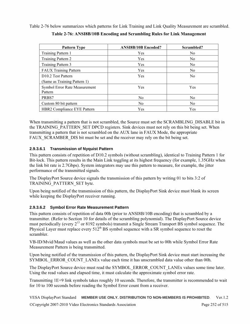
VESA DisplayPort Standard MEMBER USE ONLY. DISTRIBUTION TO NON-MEMBERS IS PROHIBITED. Ver.1.2
©Copyright 2007-2010 Video Electronics Standards Association Page 252 of 515
Table 2-76 below summarizes which patterns for Link Training and Link Quality Measurement are scrambled.
Table 2-76: ANSI8B/10B Encoding and Scrambling Rules for Link Management
Pattern Type ANSI8B/10B Encoded? Scrambled? Training Pattern 1 Yes No Training Pattern 2 Yes No Training Pattern 3 Yes No FAUX Training Pattern Yes No D10.2 Test Pattern (Same as Training Pattern 1)
Yes No
Symbol Error Rate Measurement Pattern
Yes Yes
PRBS7 No No Custom 80 bit pattern No No HBR2 Compliance EYE Pattern Yes Yes
When transmitting a pattern that is not scrambled, the Source must set the SCRAMBLING_DISABLE bit in the TRAINING_PATTERN_SET DPCD registers. Sink devices must not rely on this bit being set. When transmitting a pattern that is not scrambled on the AUX lane in FAUX Mode, the appropriate FAUX_SCRAMBER_DIS bit must be set and the receiver may rely on the bit being set.
2.9.3.6.1 Transmission of Nyquist Pattern This pattern consists of repetition of D10.2 symbols (without scrambling), identical to Training Pattern 1 for Bit-lock. This pattern results in the Main Link toggling at its highest frequency (for example, 1.35GHz when the link bit rate is 2.7Gbps). System integrators may use this pattern to measure, for example, the jitter performance of the transmitted signals.
The DisplayPort Source device signals the transmission of this pattern by writing 01 to bits 3:2 of TRAINING_PATTERN_SET byte.
Upon being notified of the transmission of this pattern, the DisplayPort Sink device must blank its screen while keeping the DisplayPort receiver running.
2.9.3.6.2 Symbol Error Rate Measurement Pattern This pattern consists of repetition of data 00h (prior to ANSI8B/10B encoding) that is scrambled by a transmitter. (Refer to Section 10 for details of the scrambling polynomial). The DisplayPort Source device must periodically (every 213 or 8192 symbols) transmit a Single Stream Transport BS symbol sequence. The Physical Layer must replace every 512th BS symbol sequence with a SR symbol sequence to reset the scrambler.
VB-ID/Mvid/Maud values as well as the other data symbols must be set to 00h while Symbol Error Rate Measurement Pattern is being transmitted.
Upon being notified of the transmission of this pattern, the DisplayPort Sink device must start increasing the SYMBOL_ERROR_COUNT_LANEx value each time it has unscrambled data value other than 00h.
The DisplayPort Source device must read the SYMBOL_ERROR_COUNT_LANEx values some time later. Using the read values and elapsed time, it must calculate the approximate symbol error rate.
Transmitting 1E+9 link symbols takes roughly 10 seconds. Therefore, the transmitter is recommended to wait for 10 to 100 seconds before reading the Symbol Error count from a receiver.
VESA DisplayPort Standard MEMBER USE ONLY. DISTRIBUTION TO NON-MEMBERS IS PROHIBITED. Ver.1.2
©Copyright 2007-2010 Video Electronics Standards Association Page 253 of 515
Symbol error rate is calculated as follows:
At 5.4 Gbps:
o Symbol Error Rate in units of 10 -9 = Error_Count / (0.54 * Measurement Period in second)
At 2.7 Gbps:
o Symbol Error Rate in units of 10 -9 = Error_Count / (0.27 * Measurement Period in second)
At 1.62 Gbps:
o Symbol Error Rate in units of 10 -9 = Error_Count / (0.162 * Measurement Period in second)
2.9.3.6.3 PRBS and Bit Pattern Refer to address 102h of DPCD Address Mapping in Table 2-75 for a detailed description of the PRBS7 bit pattern.
2.9.3.6.4 80 bit custom pattern A DisplayPort Upstream device that supports HBR2 must be capable of sending out an 80-bit repeating pattern. A DisplayPort Upstream device that does not support HBR2 may be capable of sending out an 80-bit repeating pattern. The custom pattern is not scrambled or encoded with 8b10b. The custom pattern allows for more flexibility during Physical Compliance testing of Upstream devices only (does not apply to Downstream devices).
2.9.3.6.5 HBR2 Compliance EYE Pattern A DisplayPort Upstream device that is capable of supporting HBR2 must be capable of sending the repetition of scrambled data 00h with 8B/10B encoding (Refer to Appendix E for the details of the scrambling polynomial). This capability is optional for Upstream devices that do not support HBR2. The Upstream device must output an Enhanced Framing Scrambler Reset sequence (SR BF BF SR) for every HBR2_COMPLIANCE_SCRAMBLER_RESET symbols transmitter (the count to include the four symbols comprising the scrambler reset sequence). If HBR2_COMPLIANCE_SCRAMBLER_RESET is less than 4, then no scrambler reset sequence is transmitted.
An HBR2 DisplayPort Downstream device must be capable of receiving the HBR2 Compliance EYE Pattern from test equipment. During compliance testing, the Downstream device scrambler will be reset by a SR symbol after the completion of link training. The HBR2 Downstream device must start increasing the SYMBOL_ERROR_COUNT_LANEx value each time it has unscrambled data value other than 00h.
2.9.4 AUX Device Services AUX Device Services are used for the purpose of communication between the graphic host and the display device. The following are examples of display device services that are supported by the AUX Channel:
• EDID Support
• MCCS Support
• Sink Event Notification
EDID and MCCS over DDC/CI are supported by mapping I2C transaction onto DisplayPort to maintain maximum software transparency.
In addition, the AUX CH is expected to be used for an optional content protection feature.
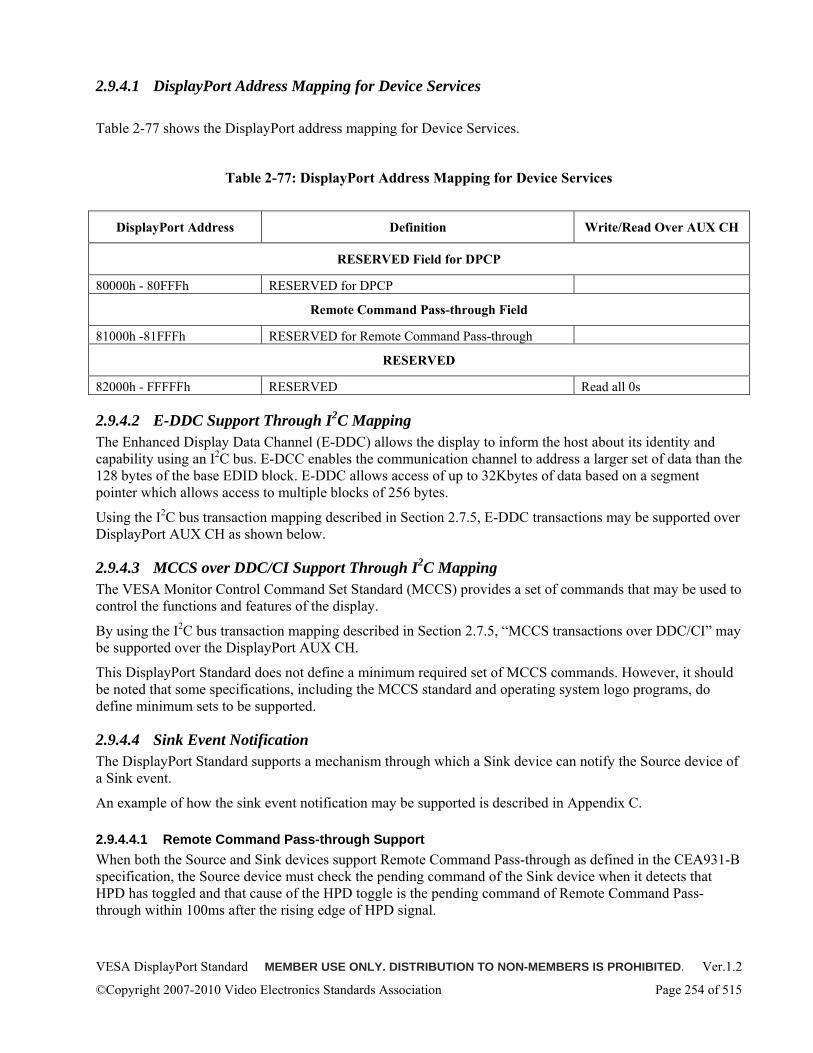
VESA DisplayPort Standard MEMBER USE ONLY. DISTRIBUTION TO NON-MEMBERS IS PROHIBITED. Ver.1.2
©Copyright 2007-2010 Video Electronics Standards Association Page 254 of 515
2.9.4.1 DisplayPort Address Mapping for Device Services
Table 2-77 shows the DisplayPort address mapping for Device Services.
Table 2-77: DisplayPort Address Mapping for Device Services
DisplayPort Address Definition Write/Read Over AUX CH
RESERVED Field for DPCP
80000h - 80FFFh RESERVED for DPCP
Remote Command Pass-through Field
81000h -81FFFh RESERVED for Remote Command Pass-through
RESERVED
82000h - FFFFFh RESERVED Read all 0s
2.9.4.2 E-DDC Support Through I2C Mapping The Enhanced Display Data Channel (E-DDC) allows the display to inform the host about its identity and capability using an I2C bus. E-DCC enables the communication channel to address a larger set of data than the 128 bytes of the base EDID block. E-DDC allows access of up to 32Kbytes of data based on a segment pointer which allows access to multiple blocks of 256 bytes.
Using the I2C bus transaction mapping described in Section 2.7.5, E-DDC transactions may be supported over DisplayPort AUX CH as shown below.
2.9.4.3 MCCS over DDC/CI Support Through I2C Mapping The VESA Monitor Control Command Set Standard (MCCS) provides a set of commands that may be used to control the functions and features of the display.
By using the I2C bus transaction mapping described in Section 2.7.5, “MCCS transactions over DDC/CI” may be supported over the DisplayPort AUX CH.
This DisplayPort Standard does not define a minimum required set of MCCS commands. However, it should be noted that some specifications, including the MCCS standard and operating system logo programs, do define minimum sets to be supported.
2.9.4.4 Sink Event Notification The DisplayPort Standard supports a mechanism through which a Sink device can notify the Source device of a Sink event.
An example of how the sink event notification may be supported is described in Appendix C.
2.9.4.4.1 Remote Command Pass-through Support When both the Source and Sink devices support Remote Command Pass-through as defined in the CEA931-B specification, the Source device must check the pending command of the Sink device when it detects that HPD has toggled and that cause of the HPD toggle is the pending command of Remote Command Pass-through within 100ms after the rising edge of HPD signal.
VESA DisplayPort Standard MEMBER USE ONLY. DISTRIBUTION TO NON-MEMBERS IS PROHIBITED. Ver.1.2
©Copyright 2007-2010 Video Electronics Standards Association Page 255 of 515
2.10 Protocol Differentiation for Embedded DisplayPort (eDP)
2.10.1 Overview In order to provide additional methods to facilitate GPU implementations that meet obligations of premium content requirements in embedded DisplayPort systems, additional features are included in this Standard. Since certain system implementations do not require features beyond those provided in DP1.1a to satisfy premium content requirements, these are optional features. These additional DP1.2 features, which optionally provide protocol-level differentiation between embedded and box-to box applications, are designed to facilitate such GPU implementations, while retaining the benefits of a unified standard spanning embedded and box-to-box applications that was provided in DisplayPort 1.1a.
2.10.2 Protocol Differentiation Methods Two alternative protocol-based methods are defined. Each may be used to ensure non-interoperability between compliant eDP Sources and non-eDP Sinks where such non-interoperability is defined as the inability to reliably convey audio or video data from Source to Sink. Specifics of how non-interoperability is achieved vary by method and implementation practice in use of each method, with such implementation practice being beyond the scope of this Standard.
Implementation of either one or both of these methods is optional for DP1.2 devices, unless otherwise explicitly stated. Consistent with other eDP practices, the system integrator is ultimately responsible for ensuring interoperability between the eDP source and sink chosen for a particular application. Determination by a given device (source, sink or branch) used in an embedded system is an implementation matter beyond the scope of this Standard.
The embedded Sink device differentiation capabilities described below shall only be implemented in devices providing eDP connections over embedded (non-user-accessible) interconnects. Tamper-resistant methods3 should be used in devices that allow operation in either eDP or Box-to-Box DisplayPort applications to be determined at manufacturing/assembly time by the system integrator.
Method 1: ALTERNATE SCRAMBLER RESET On an eDP connection the SR symbol resets the LFSRs in the Source and the Sink to FFFEh, rather than (the non-eDP connection) value FFFFh.
Method 2: FRAMING CHANGE On an eDP connection, the eDP sink must operate only in Enhanced Framing Mode. The Source must send only Enhanced Framing on the main link, and must only write a ‘0’ to DPCD 00101h: LANE_COUNT_SET Bit 7: ENHANCED_FRAME_EN bit.
DP1.2 compliant non-eDP Sinks are not permitted to interoperate with Enhanced Framing Mode signaling if DPCD 00101h: LANE_COUNT_SET Bit 7: ENHANCED_FRAME_EN bit has been set to a ‘0’
Independent of method used, DP1.2 compliant eDP Receivers shall indicate any eDP protocol differentiation method they support through the Receiver Capability Field of DPCD (DPCD:0000Dh). Note: eDP receivers may support more than one of the methods.
2.10.3 eDP Source Behavior (Informative) Source devices may configure eDP capable sinks into any mode or combination thereof, depending on the option(s) the source supports on usage (for example, during link testing). In order to provide robustness, the Source will not change the differentiation method thereafter even if the eDP Sink’s capability flag was to change.
3 For example: package bond options, fuses or external strapping options, buried vias/trace connections.
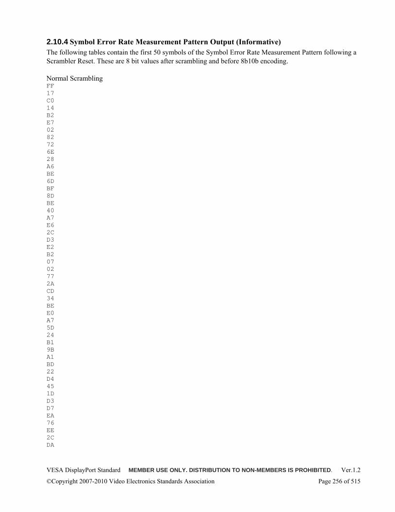
VESA DisplayPort Standard MEMBER USE ONLY. DISTRIBUTION TO NON-MEMBERS IS PROHIBITED. Ver.1.2
©Copyright 2007-2010 Video Electronics Standards Association Page 256 of 515
2.10.4 Symbol Error Rate Measurement Pattern Output (Informative) The following tables contain the first 50 symbols of the Symbol Error Rate Measurement Pattern following a Scrambler Reset. These are 8 bit values after scrambling and before 8b10b encoding. Normal Scrambling FF 17 C0 14 B2 E7 02 82 72 6E 28 A6 BE 6D BF 8D BE 40 A7 E6 2C D3 E2 B2 07 02 77 2A CD 34 BE E0 A7 5D 24 B1 9B A1 BD 22 D4 45 1D D3 D7 EA 76 EE 2C DA
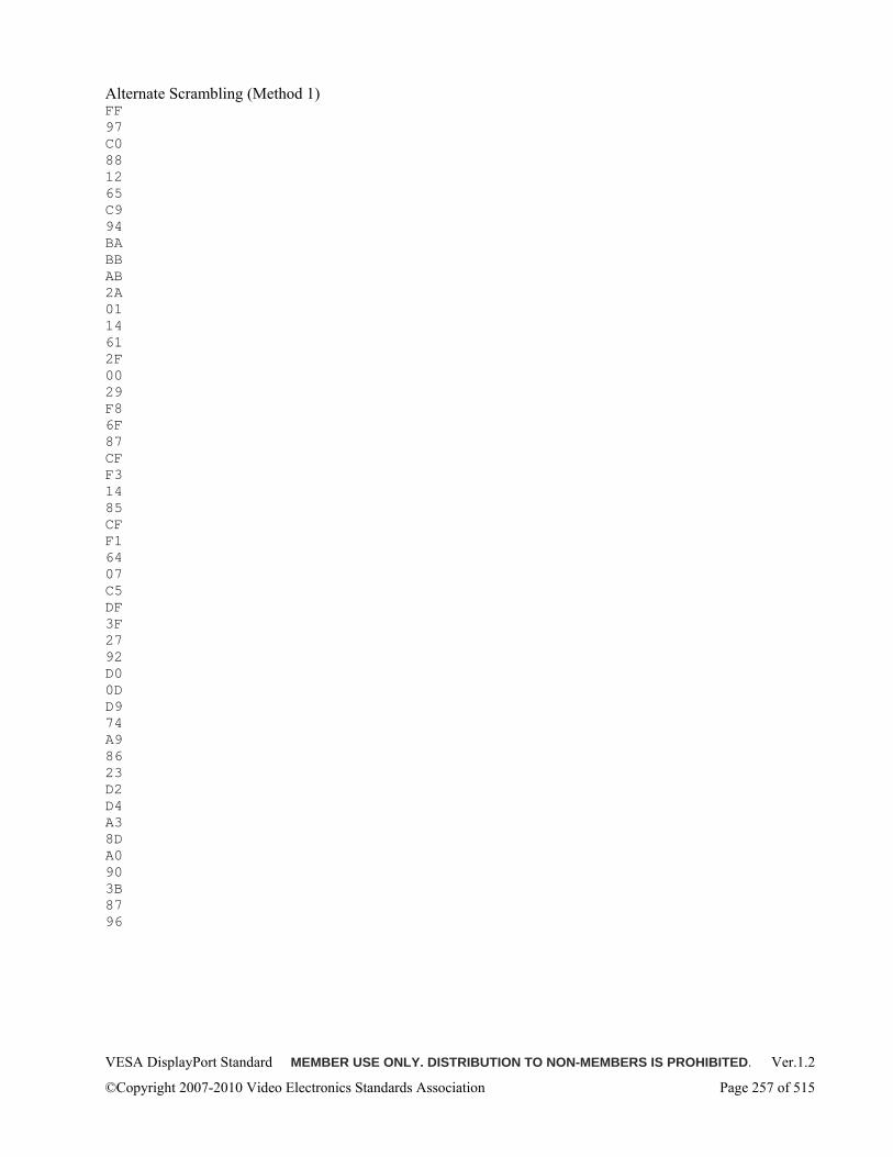
VESA DisplayPort Standard MEMBER USE ONLY. DISTRIBUTION TO NON-MEMBERS IS PROHIBITED. Ver.1.2
©Copyright 2007-2010 Video Electronics Standards Association Page 257 of 515
Alternate Scrambling (Method 1) FF 97 C0 88 12 65 C9 94 BA BB AB 2A 01 14 61 2F 00 29 F8 6F 87 CF F3 14 85 CF F1 64 07 C5 DF 3F 27 92 D0 0D D9 74 A9 86 23 D2 D4 A3 8D A0 90 3B 87 96
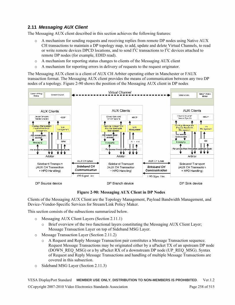
VESA DisplayPort Standard MEMBER USE ONLY. DISTRIBUTION TO NON-MEMBERS IS PROHIBITED. Ver.1.2
©Copyright 2007-2010 Video Electronics Standards Association Page 258 of 515
2.11 Messaging AUX Client The Messaging AUX client described in this section achieves the following features:
o A mechanism for sending requests and receiving replies from remote DP nodes using Native AUX CH transactions to maintain a DP topology map, to add, update and delete Virtual Channels, to read or write remote devices DPCD locations, and to send I2C transactions to I2C devices attached to remote DP nodes (for example, EDID read).
o A mechanism for reporting status changes to clients of the Messaging AUX client o A mechanism for reporting errors in delivery of requests to the request originator.
The Messaging AUX client is a client of AUX CH Arbiter operating either in Manchester or FAUX transaction format. The Messaging AUX client provides the means of communication between any two DP nodes of a topology. Figure 2-90 shows the position of the Messaging AUX client in DP nodes
Figure 2-90: Messaging AUX Client in DP Nodes
Clients of the Messaging AUX Client are the Topology Management, Payload Bandwidth Management, and Device-/Vendor-Specific Services for Stream/Link Policy Maker.
This section consists of the subsections summarized below.
o Messaging AUX Client Layers (Section 2.11.1) o Brief overview of the two functional layers constituting the Messaging AUX Client Layer;
Message Transaction Layer on top of Sideband MSG Layer. o Message Transaction Layer (Section 2.11.2)
o A Request and Reply Message Transaction pair constitutes a Message Transaction sequence. Request Message Transactions may be originated either by a uPacket TX of an upstream DP node (DOWN_REQ_MSG) or a by uPacket RX of a downstream DP node (UP_REQ_MSG). Syntax of Request and Reply Message Transactions and handling of multiple Message Transactions are covered in this subsection.
o Sideband MSG Layer (Section 2.11.3)
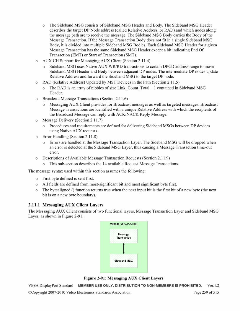
VESA DisplayPort Standard MEMBER USE ONLY. DISTRIBUTION TO NON-MEMBERS IS PROHIBITED. Ver.1.2
©Copyright 2007-2010 Video Electronics Standards Association Page 259 of 515
o The Sideband MSG consists of Sideband MSG Header and Body. The Sideband MSG Header describes the target DP Node address (called Relative Address, or RAD) and which nodes along the message path are to receive the message. The Sideband MSG Body carries the Body of the Message Transaction. If the Message Transaction Body does not fit in a single Sideband MSG Body, it is divided into multiple Sideband MSG Bodies. Each Sideband MSG Header for a given Message Transaction has the same Sideband MSG Header except a bit indicating End Of Transaction (EMT) or Start of Transaction (SMT).
o AUX CH Support for Messaging AUX Client (Section 2.11.4) o Sideband MSG uses Native AUX WR/RD transactions to certain DPCD address range to move
Sideband MSG Header and Body between adjacent DP nodes. The intermediate DP nodes update Relative Address and forward the Sideband MSG to the target DP node.
o RAD (Relative Address) Updated by MST Devices in the Path (Section 2.11.5) o The RAD is an array of nibbles of size Link_Count_Total – 1 contained in Sideband MSG
Header. o Broadcast Message Transactions (Section 2.11.6)
o Messaging AUX Client provides for Broadcast messages as well as targeted messages. Broadcast Message Transactions are identified with a unique Relative Address with which the recipients of the Broadcast Message can reply with ACK/NACK Reply Message.
o Message Delivery (Section 2.11.7) o Procedures and requirements are defined for delivering Sideband MSGs between DP devices
using Native AUX requests. o Error Handling (Section 2.11.8)
o Errors are handled at the Message Transaction Layer. The Sideband MSG will be dropped when an error is detected at the Sideband MSG Layer, thus causing a Message Transaction time-out error.
o Descriptions of Available Message Transaction Requests (Section 2.11.9) o This sub-section describes the 14 available Request Message Transactions.
The message syntax used within this section assumes the following:
o First byte defined is sent first. o All fields are defined from most-significant bit and most significant byte first. o The bytealigned () function returns true when the next input bit is the first bit of a new byte (the next
bit is on a new byte boundary).
2.11.1 Messaging AUX Client Layers The Messaging AUX Client consists of two functional layers, Message Transaction Layer and Sideband MSG Layer, as shown in Figure 2-91.
Figure 2-91: Messaging AUX Client Layers
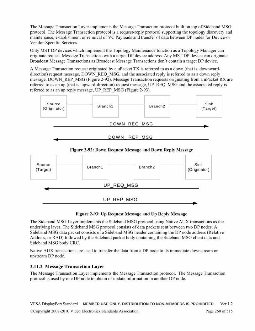
VESA DisplayPort Standard MEMBER USE ONLY. DISTRIBUTION TO NON-MEMBERS IS PROHIBITED. Ver.1.2
©Copyright 2007-2010 Video Electronics Standards Association Page 260 of 515
The Message Transaction Layer implements the Message Transaction protocol built on top of Sideband MSG protocol. The Message Transaction protocol is a request-reply protocol supporting the topology discovery and maintenance, establishment or removal of VC Payloads and transfer of data between DP nodes for Device-or Vendor-Specific Services.
Only MST DP devices which implement the Topology Maintenance function as a Topology Manager can originate request Message Transactions with a target DP device address. Any MST DP device can originate Broadcast Message Transactions as Broadcast Message Transactions don’t contain a target DP device.
A Message Transaction request originated by a uPacket TX is referred to as a down (that is, downward-direction) request message, DOWN_REQ_MSG, and the associated reply is referred to as a down reply message, DOWN_REP_MSG (Figure 2-92). Message Transaction requests originating from a uPacket RX are referred to as an up (that is, upward-direction) request message, UP_REQ_MSG and the associated reply is referred to as an up reply message, UP_REP_MSG (Figure 2-93).
Source(Originator) Branch1 Branch2 Sink
(Target)
DOW N_REQ_M SG
DOW N_ REP_M SG
Figure 2-92: Down Request Message and Down Reply Message
Source(Target) Branch1 Branch2 Sink
(Originator)
UP_REQ_MSG
UP_REP_MSG
Figure 2-93: Up Request Message and Up Reply Message
The Sideband MSG Layer implements the Sideband MSG protocol using Native AUX transactions as the underlying layer. The Sideband MSG protocol consists of data packets sent between two DP nodes. A Sideband MSG data packet consists of a Sideband MSG header containing the DP node address (Relative Address, or RAD) followed by the Sideband packet body containing the Sideband MSG client data and Sideband MSG body CRC.
Native AUX transactions are used to transfer the data from a DP node to its immediate downstream or upstream DP node.
2.11.2 Message Transaction Layer The Message Transaction Layer implements the Message Transaction protocol. The Message Transaction protocol is used by one DP node to obtain or update information in another DP node.
VESA DisplayPort Standard MEMBER USE ONLY. DISTRIBUTION TO NON-MEMBERS IS PROHIBITED. Ver.1.2
©Copyright 2007-2010 Video Electronics Standards Association Page 261 of 515
2.11.2.1 Message Transaction Protocol The Message Transaction protocol is comprised of Message Transaction sequences. There are two types of message transactions: Request and Reply Message transactions. A Request-and-Reply Message Transaction pair defines a Message Transaction sequence.
Table 2-78: Message Transaction Sequence Syntax Syntax No. of Bits
Message_Transaction_Sequence() Message_Transaction_Request() Message_Transaction_Reply()
2.11.2.2 Message_Transaction_Request () Table 2-79: Message Transaction Request Syntax
Syntax No. of Bits Message_Transaction_Request() zero Request_Identifier Request_Data()
1 7
2.11.2.2.1 Request_Identifier The Request_Identifier field specifies the information to be obtained or updated. The following table is a list of valid Request_Identifiers.
Table 2-80: Request Names and Request Identifiers Request Name Request_Identifier
LINK_ADDRESS 01h CONNECTION_STATUS_NOTIFY 02h ENUM_PATH_RESOURCES 10h ALLOCATE_PAYLOAD 11h QUERY_PAYLOAD 12h RESOURCE_STATUS_NOTIFY 13h CLEAR_PAYLOAD_ID_TABLE 14h REMOTE_DPCD_READ 20h REMOTE_DPCD_WRITE 21h REMOTE_I2C_READ 22h REMOTE_I2C_WRITE 23h POWER_UP_PHY 24h POWER_DOWN_PHY 25h SINK_EVENT_NOTIFY 30h QUERY_STREAM_ENCRYPTION_STATUS
38h
Request_Data () Request_Data is dependent upon the Request_Identifier of the request message transaction. Table 2-81 specifies the Request_Data for requests which have request data fields. The fields in Table 2-81 are defined in Section 2.11.9. Those requests not listed in Table 2-81 do not have request data.
VESA DisplayPort Standard MEMBER USE ONLY. DISTRIBUTION TO NON-MEMBERS IS PROHIBITED. Ver.1.2
©Copyright 2007-2010 Video Electronics Standards Association Page 262 of 515
Table 2-81: Request Data Syntax No. of Bits
Request_Data() if (Request_Identifier == 02h CONNECTION_STATUS_NOTIFY Port_Number zeros Global_Unique_Identifier zero Legacy_Device_Plug_status DisplayPort_Device_Plug_Status Messaging_Capability_Status Input_Port Peer_Device_Type else if (Request_Identifier == 10h) ENUM_PATH_RESOURCES Port_Number zeros else if (Request_Identifier == 11h) ALLOCATE_PAYLOAD Port_Number Number_SDP_Streams zero Virtual_Channel_Payload_Identifier Payload_Bandwidth_Number for (i = 0; i < Number_SDP_Streams; i++) SDP_Stream_Sink[i] while (!bytealigned()) zeros else if (Request_Identifier == 12h) QUERY_PAYLOAD Port_Number zeros zero Virtual_Channel_Payload_Identifier else if (Request_Identifier == 13h) RESOURCE_STATUS_NOTIFY Port_Number zeros Global_Unique_Identifier Available_PBN
4 4
128 1 1 1 1 1 3
4 4
4 4 1 7
16
4
1
4 4 1 7
4 4
128 16
VESA DisplayPort Standard MEMBER USE ONLY. DISTRIBUTION TO NON-MEMBERS IS PROHIBITED. Ver.1.2
©Copyright 2007-2010 Video Electronics Standards Association Page 263 of 515
else if (Request_Identifier == 20h) REMOTE_DPCD_READ Port_Number DPCD_Address Number_Of_Bytes_To_Read for (i = 0; i < Number_Of_Bytes_Read; i++) DPCD_Byte_Read[i] else if (Request_Identifier == 21h) REMOTE_DPCD_WRITE Port_Number DPCD_Address Number_Of_Bytes_To_Write for (i = 0; i < Number_Of_Bytes_To_Write; i++) Write_Data[i] else if (Request_Identifier == 22h) REMOTE_I2C_READ Port_Number zeros Number_Of_I2C_Transactions for (i = 0; i < Number_Of_I2C_Transactions - 1; i++) zero Write_I2C_Device_Identifier[i] Number_Of_Bytes_To_Write[i] for (j = 0; j < Number_Of_Bytes_To_Write; j++) I2C_Data_To_Write[i][j] zeros No_Stop_Bit[i] I2C_Transaction_Delay[i] zero Read_I2C_Device_Identifier[i + 1] Number_Of_Bytes_To_Read else if (Request_Identifier == 23h) REMOTE_I2C_WRITE Port_Number zeros zero Write_I2C_Device_Identifier Number_Of_Bytes_To_Write for (i = 0; i < Number_Of_Bytes_To_Write; i++) I2C_Data_To_Write else if (Request_Identifier == 24h) POWER_UP_PHY Port_Number zeros
4 20 8
8
4 20 8
8
2 2 4
1 7 8
8
3 1 4
1 7 8
4 4 1 7 8
8
4 4
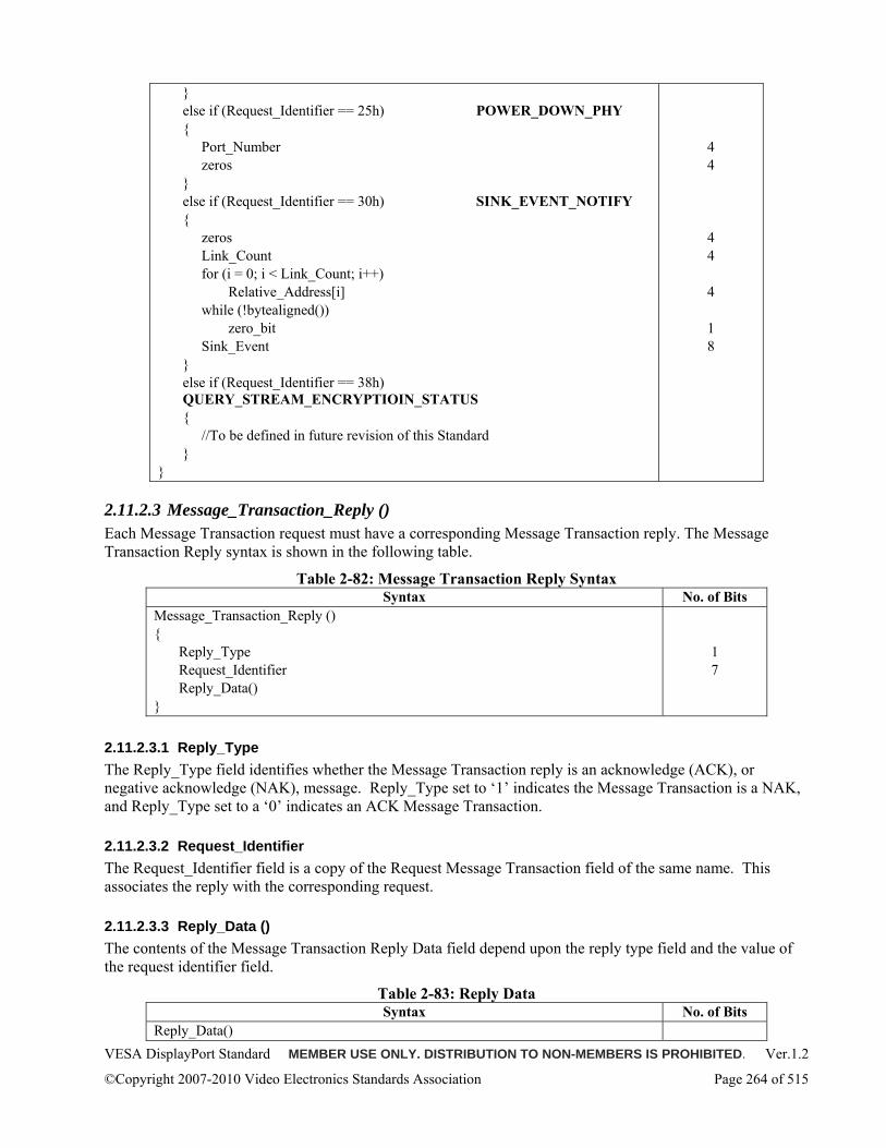
VESA DisplayPort Standard MEMBER USE ONLY. DISTRIBUTION TO NON-MEMBERS IS PROHIBITED. Ver.1.2
©Copyright 2007-2010 Video Electronics Standards Association Page 264 of 515
else if (Request_Identifier == 25h) POWER_DOWN_PHY Port_Number zeros else if (Request_Identifier == 30h) SINK_EVENT_NOTIFY zeros Link_Count for (i = 0; i < Link_Count; i++) Relative_Address[i] while (!bytealigned()) zero_bit Sink_Event else if (Request_Identifier == 38h) QUERY_STREAM_ENCRYPTIOIN_STATUS //To be defined in future revision of this Standard
4 4
4 4
4
1 8
2.11.2.3 Message_Transaction_Reply () Each Message Transaction request must have a corresponding Message Transaction reply. The Message Transaction Reply syntax is shown in the following table.
Table 2-82: Message Transaction Reply Syntax Syntax No. of Bits
Message_Transaction_Reply () Reply_Type Request_Identifier Reply_Data()
1 7
2.11.2.3.1 Reply_Type The Reply_Type field identifies whether the Message Transaction reply is an acknowledge (ACK), or negative acknowledge (NAK), message. Reply_Type set to ‘1’ indicates the Message Transaction is a NAK, and Reply_Type set to a ‘0’ indicates an ACK Message Transaction.
2.11.2.3.2 Request_Identifier The Request_Identifier field is a copy of the Request Message Transaction field of the same name. This associates the reply with the corresponding request.
2.11.2.3.3 Reply_Data () The contents of the Message Transaction Reply Data field depend upon the reply type field and the value of the request identifier field.
Table 2-83: Reply Data Syntax No. of Bits
Reply_Data()
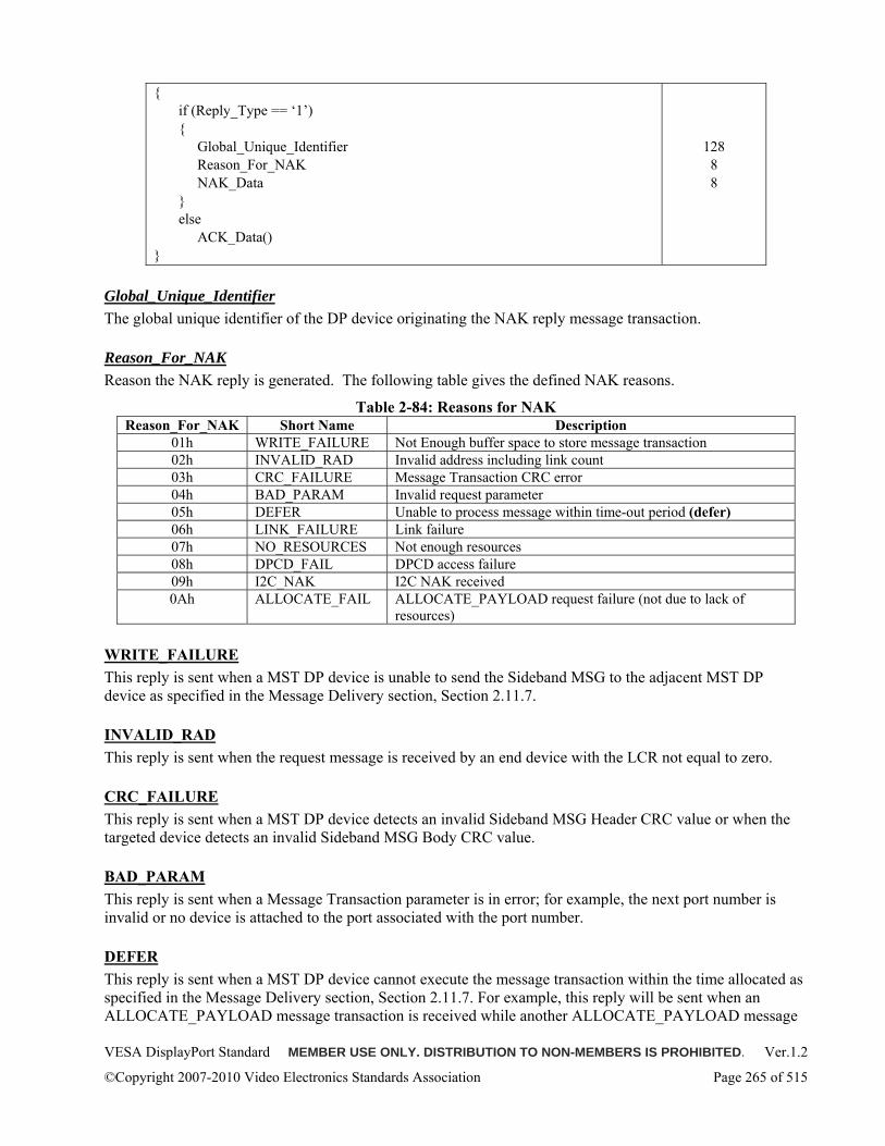
VESA DisplayPort Standard MEMBER USE ONLY. DISTRIBUTION TO NON-MEMBERS IS PROHIBITED. Ver.1.2
©Copyright 2007-2010 Video Electronics Standards Association Page 265 of 515
if (Reply_Type == ‘1’) Global_Unique_Identifier Reason_For_NAK NAK_Data else ACK_Data()
128 8 8
Global_Unique_Identifier The global unique identifier of the DP device originating the NAK reply message transaction.
Reason_For_NAK Reason the NAK reply is generated. The following table gives the defined NAK reasons.
Table 2-84: Reasons for NAK Reason_For_NAK Short Name Description
01h WRITE_FAILURE Not Enough buffer space to store message transaction 02h INVALID_RAD Invalid address including link count 03h CRC_FAILURE Message Transaction CRC error 04h BAD_PARAM Invalid request parameter 05h DEFER Unable to process message within time-out period (defer) 06h LINK_FAILURE Link failure 07h NO_RESOURCES Not enough resources 08h DPCD_FAIL DPCD access failure 09h I2C_NAK I2C NAK received 0Ah ALLOCATE_FAIL ALLOCATE_PAYLOAD request failure (not due to lack of
resources)
WRITE_FAILURE This reply is sent when a MST DP device is unable to send the Sideband MSG to the adjacent MST DP device as specified in the Message Delivery section, Section 2.11.7.
INVALID_RAD This reply is sent when the request message is received by an end device with the LCR not equal to zero.
CRC_FAILURE This reply is sent when a MST DP device detects an invalid Sideband MSG Header CRC value or when the targeted device detects an invalid Sideband MSG Body CRC value.
BAD_PARAM This reply is sent when a Message Transaction parameter is in error; for example, the next port number is invalid or no device is attached to the port associated with the port number.
DEFER This reply is sent when a MST DP device cannot execute the message transaction within the time allocated as specified in the Message Delivery section, Section 2.11.7. For example, this reply will be sent when an ALLOCATE_PAYLOAD message transaction is received while another ALLOCATE_PAYLOAD message
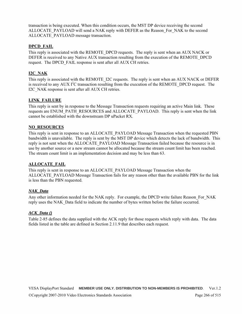
VESA DisplayPort Standard MEMBER USE ONLY. DISTRIBUTION TO NON-MEMBERS IS PROHIBITED. Ver.1.2
©Copyright 2007-2010 Video Electronics Standards Association Page 266 of 515
transaction is being executed. When this condition occurs, the MST DP device receiving the second ALLOCATE_PAYLOAD will send a NAK reply with DEFER as the Reason_For_NAK to the second ALLOCATE_PAYLOAD message transaction.
DPCD_FAIL This reply is associated with the REMOTE_DPCD requests. The reply is sent when an AUX NACK or DEFER is received to any Native AUX transaction resulting from the execution of the REMOTE_DPCD request. The DPCD_FAIL response is sent after all AUX CH retries.
I2C_NAK This reply is associated with the REMOTE_I2C requests. The reply is sent when an AUX NACK or DEFER is received to any AUX I2C transaction resulting from the execution of the REMOTE_DPCD request. The I2C_NAK response is sent after all AUX CH retries.
LINK_FAILURE This reply is sent by in response to the Message Transaction requests requiring an active Main link. These requests are ENUM_PATH_RESOURCES and ALLOCATE_PAYLOAD. This reply is sent when the link cannot be established with the downstream DP uPacket RX.
NO_RESOURCES This reply is sent in response to an ALLOCATE_PAYLOAD Message Transaction when the requested PBN bandwidth is unavailable. The reply is sent by the MST DP device which detects the lack of bandwidth. This reply is not sent when the ALLOCATE_PAYLOAD Message Transaction failed because the resource is in use by another source or a new stream cannot be allocated because the stream count limit has been reached. The stream count limit is an implementation decision and may be less than 63.
ALLOCATE_FAIL This reply is sent in response to an ALLOCATE_PAYLOAD Message Transaction when the ALLOCATE_PAYLOAD Message Transaction fails for any reason other than the available PBN for the link is less than the PBN requested.
NAK_Data Any other information needed for the NAK reply. For example, the DPCD write failure Reason_For_NAK reply uses the NAK_Data field to indicate the number of bytes written before the failure occurred.
ACK_Data () Table 2-85 defines the data supplied with the ACK reply for those requests which reply with data. The data fields listed in the table are defined in Section 2.11.9 that describes each request.
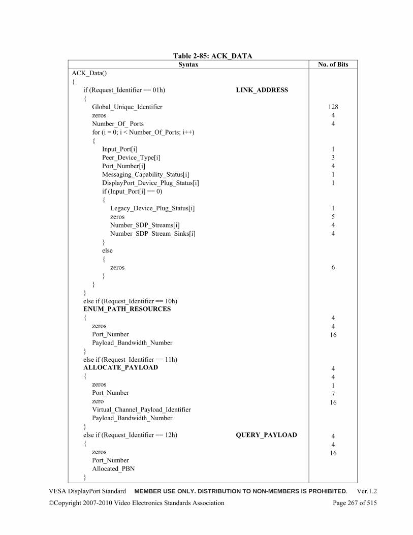
VESA DisplayPort Standard MEMBER USE ONLY. DISTRIBUTION TO NON-MEMBERS IS PROHIBITED. Ver.1.2
©Copyright 2007-2010 Video Electronics Standards Association Page 267 of 515
Table 2-85: ACK_DATA Syntax No. of Bits
ACK_Data() if (Request_Identifier == 01h) LINK_ADDRESS Global_Unique_Identifier zeros Number_Of_ Ports for (i = 0; i < Number_Of_Ports; i++) Input_Port[i] Peer_Device_Type[i] Port_Number[i] Messaging_Capability_Status[i] DisplayPort_Device_Plug_Status[i] if (Input_Port[i] == 0) Legacy_Device_Plug_Status[i] zeros Number_SDP_Streams[i] Number_SDP_Stream_Sinks[i] else zeros else if (Request_Identifier == 10h) ENUM_PATH_RESOURCES zeros Port_Number Payload_Bandwidth_Number else if (Request_Identifier == 11h) ALLOCATE_PAYLOAD zeros Port_Number zero Virtual_Channel_Payload_Identifier Payload_Bandwidth_Number else if (Request_Identifier == 12h) QUERY_PAYLOAD zeros Port_Number Allocated_PBN
128 4 4
1 3 4 1 1
1 5 4 4
6
4 4
16
4 4 1 7
16
4 4
16
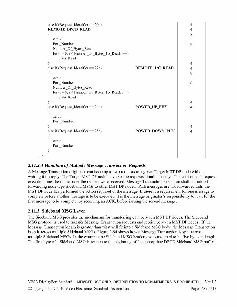
VESA DisplayPort Standard MEMBER USE ONLY. DISTRIBUTION TO NON-MEMBERS IS PROHIBITED. Ver.1.2
©Copyright 2007-2010 Video Electronics Standards Association Page 268 of 515
else if (Request_Identifier == 20h) REMOTE_DPCD_READ zeros Port_Number Number_Of_Bytes_Read for (i = 0; i < Number_Of_Bytes_To_Read; i++) Data_Read else if (Request_Identifier == 22h) REMOTE_I2C_READ zeros Port_Number Number_Of_Bytes_Read for (i = 0; i < Number_Of_Bytes_To_Read; i++) Data_Read else if (Request_Identifier == 24h) POWER_UP_PHY zeros Port_Number else if (Request_Identifier == 25h) POWER_DOWN_PHY zeros Port_Number
4 4 8
8
4 4 8
8
4 4
4 4
2.11.2.4 Handling of Multiple Message Transaction Requests A Message Transaction originator can issue up to two requests to a given Target MST DP node without waiting for a reply. The Target MST DP node may execute requests simultaneously. The start of each request execution must be in the order the request were received. Message Transaction execution shall not inhibit forwarding node type Sideband MSGs to other MST DP nodes. Path messages are not forwarded until the MST DP node has performed the action required of the message. If there is a requirement for one message to complete before another message is to be executed, it is the message originator’s responsibility to wait for the first message to be complete, by receiving an ACK, before issuing the second message.
2.11.3 Sideband MSG Layer The Sideband MSG provides the mechanism for transferring data between MST DP nodes. The Sideband MSG protocol is used to transfer Message Transaction requests and replies between MST DP nodes. If the Message Transaction length is greater than what will fit into a Sideband MSG body, the Message Transaction is split across multiple Sideband MSGs. Figure 2-94 shows how a Message Transaction is split across multiple Sideband MSGs. In the example the Sideband MSG header size is assumed to be five bytes in length. The first byte of a Sideband MSG is written to the beginning of the appropriate DPCD Sideband MSG buffer.
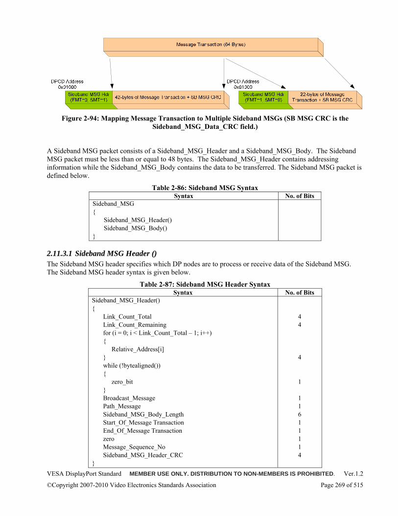
VESA DisplayPort Standard MEMBER USE ONLY. DISTRIBUTION TO NON-MEMBERS IS PROHIBITED. Ver.1.2
©Copyright 2007-2010 Video Electronics Standards Association Page 269 of 515
Figure 2-94: Mapping Message Transaction to Multiple Sideband MSGs (SB MSG CRC is the
Sideband_MSG_Data_CRC field.)
A Sideband MSG packet consists of a Sideband_MSG_Header and a Sideband_MSG_Body. The Sideband MSG packet must be less than or equal to 48 bytes. The Sideband_MSG_Header contains addressing information while the Sideband_MSG_Body contains the data to be transferred. The Sideband MSG packet is defined below.
Table 2-86: Sideband MSG Syntax Syntax No. of Bits
Sideband_MSG Sideband_MSG_Header() Sideband_MSG_Body()
2.11.3.1 Sideband MSG Header () The Sideband MSG header specifies which DP nodes are to process or receive data of the Sideband MSG. The Sideband MSG header syntax is given below.
Table 2-87: Sideband MSG Header Syntax Syntax No. of Bits
Sideband_MSG_Header() Link_Count_Total Link_Count_Remaining for (i = 0; i < Link_Count_Total – 1; i++) Relative_Address[i] while (!bytealigned()) zero_bit Broadcast_Message Path_Message Sideband_MSG_Body_Length Start_Of_Message Transaction End_Of_Message Transaction zero Message_Sequence_No Sideband_MSG_Header_CRC
4 4
4
1
1 1 6 1 1 1 1 4
VESA DisplayPort Standard MEMBER USE ONLY. DISTRIBUTION TO NON-MEMBERS IS PROHIBITED. Ver.1.2
©Copyright 2007-2010 Video Electronics Standards Association Page 270 of 515
2.11.3.1.1 Link_Count_Total (LCT) Link_Count_Total is the total number of DP links a Sideband MSG traverses from message originator to message target. The maximum value for Link_Count_Total is 15. Therefore, the total number of physical and logical DP links is 15. The total number of physical DP links is limited to seven.
2.11.3.1.2 Link_Count_Remaining (LCR) Link_Count_Remaining is the remaining number of DP links a Sideband MSG must traverse to reach the message target. The Link_Count_Remaining value is initialized to the Link_Count_Total value by the originator Sideband MSG layer. Along the message path, the uPacket TX device while forwarding the Sideband MSG decrements the Link_Count_Remaining value by one. The Link_Count_Remaining value is equal to Link_Count_Total – 1 when the message arrives at the first DP node from the message originator.
2.11.3.1.3 Relative_Address (RAD) The Relative_Address is the address of a DP node relative to the originator of the Sideband MSG. How the Relative Address (RAD) is updated by intermediate MST devices along the path of the Message Transaction to a target device is described in Section 2.11.5.
2.11.3.1.4 Sideband_MSG_Body_Length The Sideband_MSG_Body_Length gives the number of bytes contained in the Sideband MSG body. The Message Transaction length being transferred is the sum of the Sideband_MSG_Body_Length field - 1 for each Sideband MSG needed to transfer the Message Transaction.
2.11.3.1.5 Start_Of_Message Transaction (SMT) When set to one, Start_Of_Message_Transaction bit indicates current Sideband MSG contains the first Sideband MSG of a Message Transaction.
2.11.3.1.6 End_Of_Message_Transaction (EMT) When set to one, End_Of_Message_Transaction bit indicates the current Sideband MSG is the last Sideband MSG for the current message transaction. This bit will be set to one even if the current message transaction requires only one Sideband MSG.
2.11.3.1.7 Path_Message When set to one, the Path_Message bit indicates all MST DP nodes between the originator and the target are required to read and react to the data in the Sideband MSG data area. When set to zero, intermediate DP nodes along the message transaction path may still need to modify the data within the Sideband MSG data area, but the data is only targeted for the target MST DP node. All MST DP nodes along the Sideband MSG path must modify the relative address and Link Count Remaining fields (LCR) as stated in Sections 2.11.3.1.3 and 2.11.3.1.2, regardless of the state of the Path_Message bit. A DP device can only execute one path message at a time regardless of the source of the message.
2.11.3.1.8 Message_Sequence_No The Message_Sequence_No (MSN), bit identifies individual Message Transactions to a given DP device. A DP Message Transaction originator can’t send two Message Transactions with the same MSN to the same DP device without a reply to the first Message Transaction being received first.
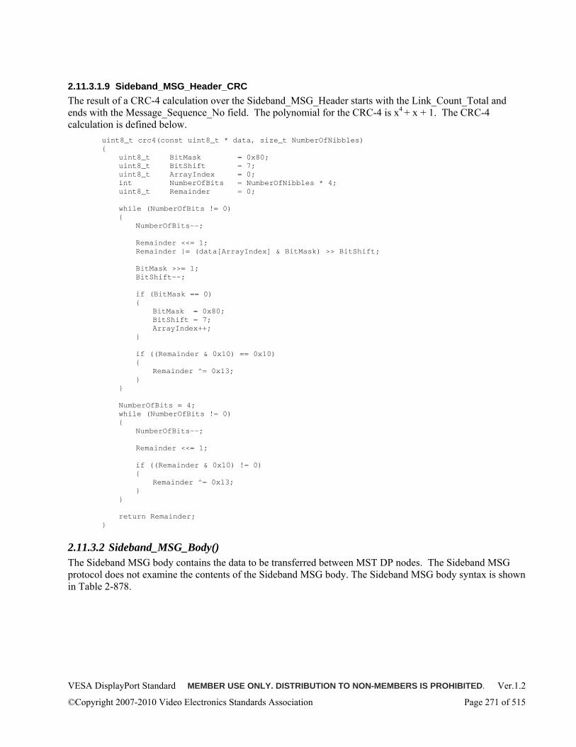
VESA DisplayPort Standard MEMBER USE ONLY. DISTRIBUTION TO NON-MEMBERS IS PROHIBITED. Ver.1.2
©Copyright 2007-2010 Video Electronics Standards Association Page 271 of 515
2.11.3.1.9 Sideband_MSG_Header_CRC The result of a CRC-4 calculation over the Sideband_MSG_Header starts with the Link_Count_Total and ends with the Message_Sequence_No field. The polynomial for the CRC-4 is x4 + x + 1. The CRC-4 calculation is defined below.
uint8_t crc4(const uint8_t * data, size_t NumberOfNibbles) uint8_t BitMask = 0x80; uint8_t BitShift = 7; uint8_t ArrayIndex = 0; int NumberOfBits = NumberOfNibbles * 4; uint8_t Remainder = 0; while (NumberOfBits != 0) NumberOfBits--; Remainder <<= 1; Remainder |= (data[ArrayIndex] & BitMask) >> BitShift; BitMask >>= 1; BitShift--; if (BitMask == 0) BitMask = 0x80; BitShift = 7; ArrayIndex++; if ((Remainder & 0x10) == 0x10) Remainder ^= 0x13; NumberOfBits = 4; while (NumberOfBits != 0) NumberOfBits--; Remainder <<= 1; if ((Remainder & 0x10) != 0) Remainder ^= 0x13; return Remainder;
2.11.3.2 Sideband_MSG_Body() The Sideband MSG body contains the data to be transferred between MST DP nodes. The Sideband MSG protocol does not examine the contents of the Sideband MSG body. The Sideband MSG body syntax is shown in Table 2-878.
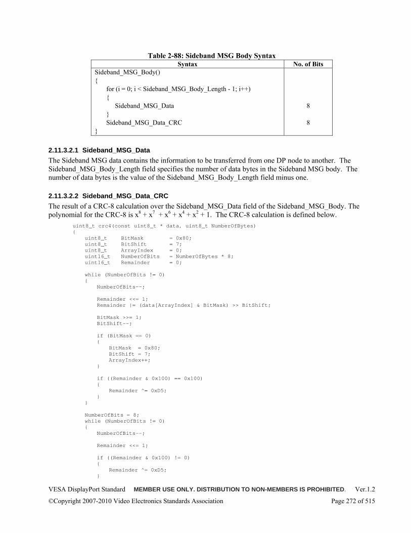
VESA DisplayPort Standard MEMBER USE ONLY. DISTRIBUTION TO NON-MEMBERS IS PROHIBITED. Ver.1.2
©Copyright 2007-2010 Video Electronics Standards Association Page 272 of 515
Table 2-88: Sideband MSG Body Syntax Syntax No. of Bits
Sideband_MSG_Body() for (i = 0; i < Sideband_MSG_Body_Length - 1; i++) Sideband_MSG_Data Sideband_MSG_Data_CRC
8
8
2.11.3.2.1 Sideband_MSG_Data The Sideband MSG data contains the information to be transferred from one DP node to another. The Sideband_MSG_Body_Length field specifies the number of data bytes in the Sideband MSG body. The number of data bytes is the value of the Sideband_MSG_Body_Length field minus one.
2.11.3.2.2 Sideband_MSG_Data_CRC The result of a CRC-8 calculation over the Sideband_MSG_Data field of the Sideband_MSG_Body. The polynomial for the CRC-8 is x8 + x7 + x6 + x4 + x2 + 1. The CRC-8 calculation is defined below.
uint8_t crc4(const uint8_t * data, uint8_t NumberOfBytes) uint8_t BitMask = 0x80; uint8_t BitShift = 7; uint8_t ArrayIndex = 0; uint16_t NumberOfBits = NumberOfBytes * 8; uint16_t Remainder = 0; while (NumberOfBits != 0) NumberOfBits--; Remainder <<= 1; Remainder |= (data[ArrayIndex] & BitMask) >> BitShift; BitMask >>= 1; BitShift--; if (BitMask == 0) BitMask = 0x80; BitShift = 7; ArrayIndex++; if ((Remainder & 0x100) == 0x100) Remainder ^= 0xD5; NumberOfBits = 8; while (NumberOfBits != 0) NumberOfBits--; Remainder <<= 1; if ((Remainder & 0x100) != 0) Remainder ^= 0xD5;
VESA DisplayPort Standard MEMBER USE ONLY. DISTRIBUTION TO NON-MEMBERS IS PROHIBITED. Ver.1.2
©Copyright 2007-2010 Video Electronics Standards Association Page 273 of 515
return Remainder & 0xFF;
2.11.4 AUX CH Support for Messaging AUX Client Sideband MSG packets move from MST DP node to node using Native AUX CH read and write transactions. In the following AUX will be used to indicate both AUX and FAUX.
2.11.4.1 Messaging AUX Client DPCD Locations Refer to Section 2.9 for the following DPCD locations associated with the Messaging AUX client.
2.11.4.1.1 MST_CAP Bit of the MSTM_CAP DPCD Location The MST_CAP bit field specifies whether the MST DP uPacket RX device supports the Messaging framework. If the DP uPacket RX indicates it supports the Messaging framework, it must be ready to accept Message Transactions from a MST DP uPacket TX. MST DP Sink devices without branching units expecting to receive data on the main link using MST packets must support the Messaging framework and set the MST_CAP bit to one.
2.11.4.1.2 UP_REQ_EN Bit of the MSTM_CTRL DPCD Location UP_REQ_EN bit field specifies whether the MST DP uPacket TX device accepts and responds to UP Sideband MSGs. Once the MST DP uPacket TX sets the UP_REQ_EN bit to ‘1’, it must be ready to accept and reply to Message Transactions from a MST DP uPacket RX .
2.11.4.1.3 DOWN_REP_MSG_RDY Bit of the DEVICE_SERVICE_IRQ_VECTOR DPCD Location The MST DP uPacket RX device sets the DOWN_REP_MSG_RDY bit to a ‘1’ after a valid Sideband DOWN_REP_MSG is written to the DOWN_REP DPCD locations. Once the DOWN_REP_MSG_RDY bit is set, the MST DP uPacket RX issues a HPD_IRQ to the connected MST DP uPacket TX.
When the MST DP uPacket TX device detects the HPD_IRQ, the MST DP uPacket TX reads the DEVICE_SERVICE_IRQ_VECTOR checking whether the DOWN_REP_MSG_RDY bit is set to ‘1’. If the DOWN_REP_MSG_RDY bit is set to a ‘1’, the Sideband DOWN_REP_MSG is read from the MST DP uPacket RX DOWN_REP DPCD locations. The DP uPacket TX device must clear the DOWN_REQ_MSG_RDY bit to ‘0’ when reading of the message is complete.
The MST DP uPacket TX device is not required to wait for the HPD_IRQ signal. The MST DP uPacket TX device can poll the appropriate MST DP uPacket RX device DPCD locations to determine if any action is required. The MST DP uPacket RX is required to generate the HPD_IRQ signal regardless of whether the MST DP uPacket TX device supports detecting the HPD_IRQ signal.
2.11.4.1.4 UP_REQ_MSG_RDY bit of the DEVICE_SERVICE_IRQ_VECTOR DPCD location The MST DP uPacket RX device sets the UP_REQ_MSG_RDY bit to a ‘1’ after a valid Sideband UP_REQ_MSG is written to the MST UP_REQ DPCD locations. Once the UP_REQ_MSG_RDY bit is set, the MST DP uPacket RX issues a HPD_IRQ to the connected MST DP uPacket TX.
When the MST DP uPacket TX device detects the HPD_IRQ, the MST DP uPacket TX reads the DEVICE_SERVICE_IRQ_VECTOR checking whether the UP_REQ_MSG_RDY bit is set to ‘1’. If the UP_REQ_MSG_RDY bit is set to a ‘1’, the Sideband UP_REQ_MSG is read from the MST DP uPacket RX UP_REQ DPCD locations. The MST DP uPacket TX device must clear the UP_REQ_MSG_RDY bit to ‘0’ when reading of the message is complete.
The MST DP uPacket TX device is not required to support detecting of the HPD_IRQ signal. The MST DP uPacket TX device can poll the appropriate MST DP uPacket RX device DPCD locations to determine if any
VESA DisplayPort Standard MEMBER USE ONLY. DISTRIBUTION TO NON-MEMBERS IS PROHIBITED. Ver.1.2
©Copyright 2007-2010 Video Electronics Standards Association Page 274 of 515
action is required. The MST DP uPacket RX is required to generate the HPD_IRQ signal regardless of whether the MST DP uPacket TX device supports detecting the HPD_IRQ signal.
2.11.4.1.5 DOWN_REQ Sideband MSG Buffer The Sideband DOWN_REQ Sideband MSG buffer holds the request Sideband MSG written by a MST DP uPacket TX device to be processed by the MST DP uPacket RX device. The first byte of the Sideband MSG containing the beginning of the Message Transaction is always written to the start address of the DOWN_REQ Sideband MSG DPCD. An MST DP Sink device is required to support the DOWN_REQ and DOWN_REP Sideband MSG buffers if it expects to receive data on the main link using MST packets. All MST DP Branch devices must support the DOWN_REQ Sideband MSG buffer for each MST DP uPacket RX.
2.11.4.1.6 UP_REP Sideband MSG Buffer The UP_REP Sideband MSG buffer holds the reply Sideband MSG written by a MST DP uPacket TX device to be processed by the MST DP uPacket RX device. The first byte of the Sideband MSG containing the beginning of the Message Transaction is always written to the start address of the UP_REP Sideband MSG DPCD. A MST DP Sink device is not required to support the UP_REQ and UP_REP Sideband MSG buffers if it does not originate Sideband MSG transactions. All MST DP Branch devices must support the UP_REP Sideband MSG buffer for each MST DP uPacket RX.
2.11.4.1.7 DOWN_REP Sideband MSG Buffer The Sideband DOWN_REP Sideband MSG buffer holds the reply Sideband MSG written by a MST DP uPacket RX device to be processed by the MST DP uPacket TX device. The first byte of the Sideband MSG containing the beginning of the Message Transaction is always written to the start address of the DOWN_REP Sideband MSG DPCD. An MST DP Sink device is required to support the DOWN_REP Sideband MSG buffer if it expects to receive data on the main link using MST packets. All MST DP Branch devices must support the DOWN_REP Sideband MSG buffer for each MST DP uPacket RX.
2.11.4.1.8 UP_REQ Sideband MSG Buffer The Sideband UP_REQ Sideband MSG buffer holds the request Sideband MSG written by a MST DP uPacket RX device to be processed by the MST DP uPacket TX device. The first byte of the Sideband MSG containing the beginning of the Message Transaction is always written to the start address of the UP_REQ Sideband MSG DPCD. An MST DP Sink device is required to support the UP_REQ Sideband MSG buffer and corresponding UP_REP Sideband MSG Buffer if the DP Sink device supports UP_REQ Sideband MSG transactions. All MST DP Branch devices must support the UP_REQ Sideband MSG buffer for each MST DP uPacket RX.
2.11.5 RAD (Relative Address) Updated by MST Devices in the Path The RAD is an array of nibbles of size Link_Count_Total – 1 contained in Sideband MSG Header as described in Section 2.11.3.1. Each nibble of the Relative_Address field specifies the port number of each DP node uPacket RX or TX the message is being sent to. When the message arrives at a DP node, Relative_Address[0] is the port number of the uPacket TX or RX within the node to send the message. Relative_Address[0] is the first port number sent as part of the RAD. Each node modifies the Relative_Address array as described with the following code sample.
for (i = 0; i < Link_Count_Remaining – 1; i++) Relative_Address[i] = Relative_Address[i + 1]; Relative_Address[i] = Input_Port_Number;
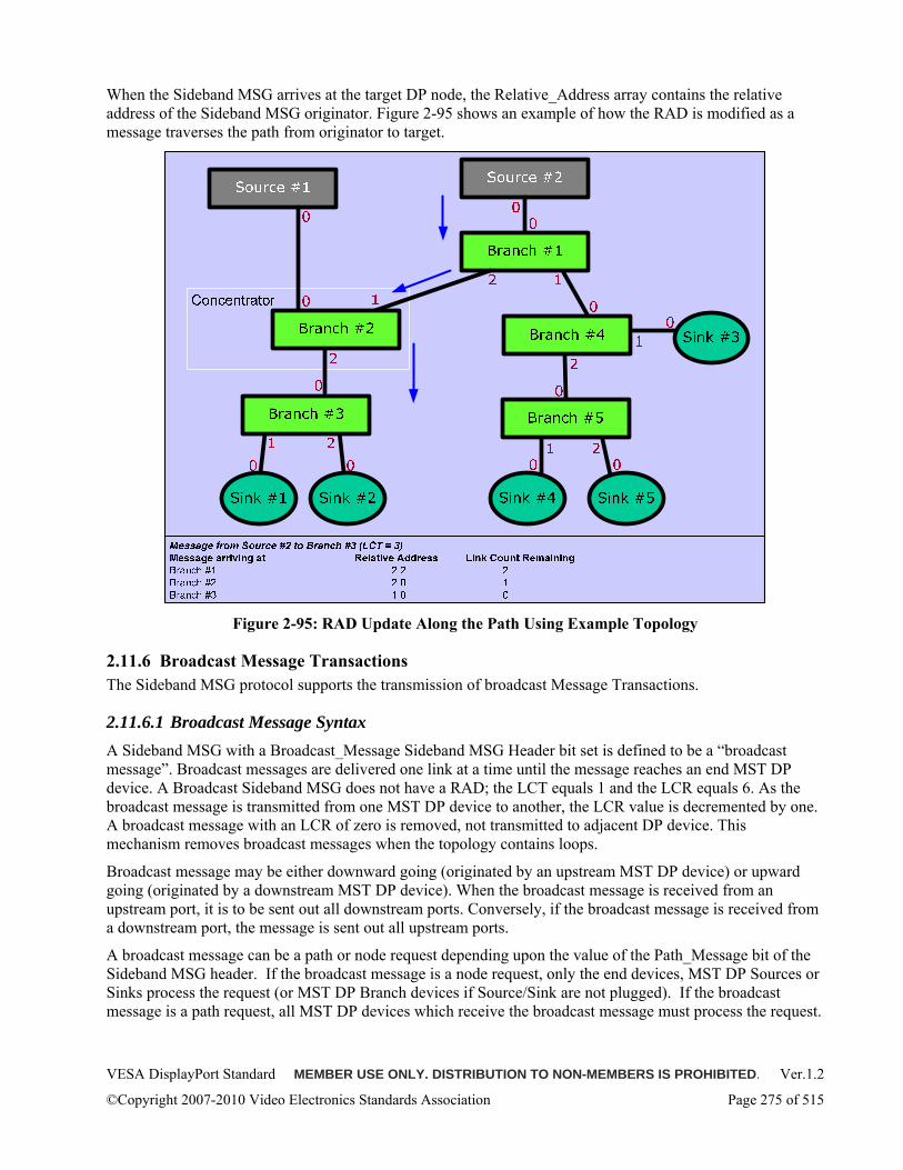
VESA DisplayPort Standard MEMBER USE ONLY. DISTRIBUTION TO NON-MEMBERS IS PROHIBITED. Ver.1.2
©Copyright 2007-2010 Video Electronics Standards Association Page 275 of 515
When the Sideband MSG arrives at the target DP node, the Relative_Address array contains the relative address of the Sideband MSG originator. Figure 2-95 shows an example of how the RAD is modified as a message traverses the path from originator to target.
Figure 2-95: RAD Update Along the Path Using Example Topology
2.11.6 Broadcast Message Transactions The Sideband MSG protocol supports the transmission of broadcast Message Transactions.
2.11.6.1 Broadcast Message Syntax A Sideband MSG with a Broadcast_Message Sideband MSG Header bit set is defined to be a “broadcast message”. Broadcast messages are delivered one link at a time until the message reaches an end MST DP device. A Broadcast Sideband MSG does not have a RAD; the LCT equals 1 and the LCR equals 6. As the broadcast message is transmitted from one MST DP device to another, the LCR value is decremented by one. A broadcast message with an LCR of zero is removed, not transmitted to adjacent DP device. This mechanism removes broadcast messages when the topology contains loops.
Broadcast message may be either downward going (originated by an upstream MST DP device) or upward going (originated by a downstream MST DP device). When the broadcast message is received from an upstream port, it is to be sent out all downstream ports. Conversely, if the broadcast message is received from a downstream port, the message is sent out all upstream ports.
A broadcast message can be a path or node request depending upon the value of the Path_Message bit of the Sideband MSG header. If the broadcast message is a node request, only the end devices, MST DP Sources or Sinks process the request (or MST DP Branch devices if Source/Sink are not plugged). If the broadcast message is a path request, all MST DP devices which receive the broadcast message must process the request.
VESA DisplayPort Standard MEMBER USE ONLY. DISTRIBUTION TO NON-MEMBERS IS PROHIBITED. Ver.1.2
©Copyright 2007-2010 Video Electronics Standards Association Page 276 of 515
2.11.6.2 Broadcast Message Reply Broadcast Message Transactions (consisting of one or multiple broadcast messages) must be replied to by the adjacent MST DP device receiving the message. The validity of the Sideband MSG header is verified along with the validity of the Sideband MSG body CRC. If an error is found, a NAK message is sent to the transmitter of the message indicating the error found. The adjacent MST DP device must retry forwarding broadcast message five times before replying with NAK. The transmitter resolves the error and sends the message again. If no error is found, an ACK reply is sent to the transmitter and no further action is required by the transmitter.
2.11.7 Message Delivery The procedures and requirements for delivering Sideband MSGs from one DP device to another are described in the following sections. The procedures and requirements are given based upon whether the DP device is the message originating device, the message target device or the message forwarding device.
2.11.7.1 Message Originating Device
2.11.7.1.1 Down Request Message The originator first ensures it has not sent a Message Transaction to the same DP device with the next Message Sequence Number (MSN). If a reply has not been received from the two previous Message Transaction requests, wait for a reply or time-out from one of the two outstanding requests. Use the freed MSN for the Message Transaction to be sent. If there is a requirement that Message Transactions are executed in a defined order, it is the responsibility of the originator to ensure the Message Transaction execution by waiting for a reply before sending subsequent messages.
The Message Transaction request is split into the required number of Sideband MSGs. The SMT bit is set in the Sideband MSG header of the first Sideband MSG of the Message Transaction request, and the EMT bit is set in the Sideband MSG header of the last Sideband MSG. If the Message Transaction request can be delivered with one Sideband MSG, the SMT and EMT bits are set in the Sideband MSG header.
The originating device will attempt to write the first Sideband MSG into the DPCD DOWN_REQ Sideband MSG Buffer using Native AUX requests. If the receiving device replies with an AUX_DEFER, retry sending the Sideband MSG an implementation-specific number of times. If the receiving device replies with an AUX_ACK, continue writing the remaining Message Transaction Sideband MSGs. Wait four seconds for a reply from the target after successfully writing the last Message Transaction Sideband MSG.
2.11.7.1.2 Up Request Message If a reply has not been received from the two previous Message Transaction requests, wait for a reply or time-out from one of the two outstanding requests. Use the freed MSN for the Message Transaction to be sent. The originator is responsible for ensuring that messages are executed in a given order by waiting for a reply before sending subsequent messages.
The Message Transaction request is split into the required number of Sideband MSGs. The SMT bit is set in the Sideband MSG header of the first Sideband MSG of the Message Transaction request, and the EMT bit is set in the Sideband MSG header of the last Sideband MSG. If the Message Transaction request can be delivered with one Sideband MSG, the SMT and EMT bits are set in the Sideband MSG header.
The originating device will write the first Sideband MSG into the DPCD UP_REQ Sideband MSG Buffer, write a one to the UpReqRdy DPCD bit and generate an IRQ_HPD to the upstream DP device. After 110ms, or after the upstream DP device writes a zero to the UpReqRdy DPCD bit, ensure the UpReqRdy DPCD bit is clear before removing the Sideband MSG from the DPCD UP_REQ Sideband MSG Buffer. The originating DP device waits four seconds for a reply after the upstream device reads the last Message Transaction Sideband MSG.
VESA DisplayPort Standard MEMBER USE ONLY. DISTRIBUTION TO NON-MEMBERS IS PROHIBITED. Ver.1.2
©Copyright 2007-2010 Video Electronics Standards Association Page 277 of 515
2.11.7.2 Message Forwarding Device (Forward and Execute if Path Message)
2.11.7.2.1 Down Request Message Transaction If there are at least 48 bytes available for reception of a Sideband MSG, reply with an AUX_ACK to the Native AUX request to write a Sideband MSG into the DPCD DOWN_REQ Sideband MSG Buffer. If there is not 48 bytes free when the first Sideband MSG Native AUX WR request is performed, reply with an AUX_DEFER until 48 bytes are available.
After the last Sideband MSG Native AUX write, check the validity of the Sideband MSG header by validating the Sideband MSG Header CRC. Check the LCR and Path bit to determine whether the Sideband MSG is to be forwarded or is part of a Message Transaction request to be executed locally. If the Sideband MSG is to be forwarded, attempt to write the Sideband MSG to the DPCD DOWN_REQ Sideband MSG Buffer of the downstream DP device using Native AUX requests. After attempting to forward for 20ms, reply to the Message Transaction originator with a Message Transaction NAK reply.
If the Sideband MSG is part of a Path Message Transaction, combine this Sideband MSG with any other Sideband MSGs for the same Message Transaction until the EMT Sideband MSG Header bit is set. After receiving the last Message Transaction Sideband MSG, execute the Message Transaction within 50ms. After executing the Message Transaction, attempt to write the Sideband MSG to the DPCD DOWN_REQ Sideband MSG Buffer of the downstream DP device using Native AUX requests. After attempting to forward for 20ms, reply to the Message Transaction originator with a Message Transaction NAK reply.
See Section 2.11.7.3.1 for handling of Node Message Transactions targeted for this DP device.
2.11.7.2.2 Down Reply Message Transaction Upon detecting an IRQ_HPD, send Native AUX requests to read the DPCD DnRplyRdy bit to determine if a Down Reply Message Transaction must be read. If down reply available, read the reply from the DPCD DOWN_REP Sideband MSG Buffer and clear the DPCD DnRplyRdy bit within 100ms of receiving the IRQ_HPD. The downstream DP device will clear the DPCD DnRplyRdy bit and clear the Sideband MSG from the DPCD DOWN_REP Sideband MSG Buffer after 110ms from the end of the IRQ_HPD pulse.
After last Sideband MSG Native AUX read, check the validity of the Sideband MSG header by validating the Sideband MSG Header CRC. Check the LCR and Path bit to determine whether the Sideband MSG is to be forwarded or is part of a Message Transaction request to be executed locally. If the Sideband MSG is to be forwarded, write the Sideband MSG to the DPCD DOWN_REP Sideband MSG Buffer, write a one to the DPCD DnRplyRdy bit and generate an IRQ_HPD within 5ms of last Sideband MSG Native AUX RD request. After 110ms or after the upstream DP device writes a zero to the DnRplyRdy DPCD bit, ensure the DnRplyRdy DPCD bit is clear before removing the Sideband MSG from the DPCD DOWN_REP Sideband MSG Buffer.
If the Sideband MSG is part of a Path Message Transaction, combine this Sideband MSG with any other Sideband MSGs for the same Message Transaction until the EMT Sideband MSG Header bit is set. After receiving the last Message Transaction Sideband MSG, execute the Message Transaction within 50ms. Once execution is complete, write the Message Transaction Sideband MSG to the DOWN_REP Sideband MSG Buffer, write a one to the DPCD DnRplyRdy bit and generate an IRQ_HPD within 5ms of last Sideband MSG Native AUX RD request. After 110ms or after the upstream DP device writes a zero to the DnRplyRdy DPCD bit, ensure the DnRplyRdy DPCD bit is clear before removing the Sideband MSG from the DPCD DOWN_REP Sideband MSG Buffer.
2.11.7.2.3 Up Request Message Transaction Upon detecting an IRQ_HPD, send Native AUX requests to read the DPCD UpReqRdy bit to determine if an Up Request Message Transaction must be read. If an up request is available, read the request Sideband MSG from the DPCD UP_REQ Sideband MSG Buffer and clear the DPCD UpReqRdy bit within 100ms of
VESA DisplayPort Standard MEMBER USE ONLY. DISTRIBUTION TO NON-MEMBERS IS PROHIBITED. Ver.1.2
©Copyright 2007-2010 Video Electronics Standards Association Page 278 of 515
receiving the IRQ_HPD. The downstream DP device will clear the DPCD UpReqRdy bit and clear the Sideband MSG from the DPCD UP_REQ Sideband MSG Buffer after 110ms from the end of the IRQ_HPD pulse.
After last Sideband MSG Native AUX read, check the validity of the Sideband MSG header by validating the Sideband MSG Header CRC. Check the LCR and Path bit to determine whether the Sideband MSG is to be forwarded or is part of a Message Transaction request to be executed locally. If the Sideband MSG is to be forwarded, write the Sideband MSG to the DPCD UP_REQ Sideband MSG Buffer, write a one to the DPCD UpReqRdy bit and generate an IRQ_HPD within 5ms of last Sideband MSG Native AUX RD request. After 110ms or after the upstream DP device writes a zero to the UpReqRdy DPCD bit, ensure the UpReqRdy DPCD bit is clear before removing the Sideband MSG from the DPCD UP_REQ Sideband MSG Buffer.
If the Sideband MSG is part of a Path Message Transaction, combine this Sideband MSG with any other Sideband MSGs for the same Message Transaction until the EMT Sideband MSG Header bit is set. After receiving the last Message Transaction Sideband MSG, execute the Message Transaction within 50ms. Once execution is complete, write the Message Transaction Sideband MSG to the UP_REQ Sideband MSG Buffer, write a one to the DPCD UpReqRdy bit and generate an IRQ_HPD within 5ms of last Sideband MSG Native AUX RD request. After 110ms or after the upstream DP device writes a zero to the UpReqRdy DPCD bit, ensure the UpReqRdy DPCD bit is clear before removing the Sideband MSG from the DPCD UP_REQ Sideband MSG Buffer. If the Up Request Message Transaction Sideband MSG was not read within 110ms by the upstream DP device, send a Message Transaction NAK to the originating device.
See Section 2.11.7.3.2 for handling of Up Node Message Transactions targeted for this DP device.
2.11.7.2.4 Up Reply Message Transaction If there is at least 48 bytes available for reception of a Sideband MSG, reply with an AUX_ACK to the Native AUX CH request to write a Sideband MSG into the DPCD UP_REP Sideband MSG Buffer. If there are not 48 bytes free when the first Sideband MSG Native AUX WR request is performed, reply with an AUX_DEFER until 48 bytes are available.
After the last Sideband MSG Native AUX write, check the validity of the Sideband MSG header by validating the Sideband MSG Header CRC. Check the LCR and Path bit to determine whether the Sideband MSG is to be forwarded or is part of a Message Transaction request to be executed locally. If the Sideband MSG is to be forwarded, attempt to write the Sideband MSG to the DPCD UP_REP Sideband MSG Buffer of the downstream DP device using Native AUX requests. Time-out after attempting to forward for 20ms and discard the Sideband MSG.
If the Sideband MSG is part of a Path Message Transaction, combine this Sideband MSG with any other Sideband MSGs for the same Message Transaction until the EMT Sideband MSG Header bit is set. After receiving the last Message Transaction Sideband MSG, execute the Message Transaction within 50ms. After executing the Message Transaction, attempt to write the Sideband MSG reply to the DPCD UP_REP Sideband MSG Buffer of the downstream DP device using Native AUX requests. Time-out after attempting to write the Message Transaction Sideband MSG reply for 20ms and discard the Message Transaction Sideband MSGs.
2.11.7.3 Message Targeted Device
2.11.7.3.1 Down Request Message If there are at least 48 bytes available for reception of a Sideband MSG, reply with an AUX_ACK to the Native AUX request to write a Sideband MSG into the DPCD DOWN_REQ Sideband MSG Buffer. If there are not 48 bytes free when the first Sideband MSG Native AUX WR request is performed, reply with an AUX_DEFER until 48 bytes are available.
VESA DisplayPort Standard MEMBER USE ONLY. DISTRIBUTION TO NON-MEMBERS IS PROHIBITED. Ver.1.2
©Copyright 2007-2010 Video Electronics Standards Association Page 279 of 515
After last Sideband MSG Native AUX read, check the validity of the Sideband MSG header by validating the Sideband MSG Header CRC. Check the LCR and Path bit to determine whether the Sideband MSG is to be forwarded or is part of a Message Transaction request to be executed locally. If the Sideband MSG is part of a Node Message Transaction to be executed locally, combine this Sideband MSG with any other Sideband MSGs for the same Message Transaction until the EMT Sideband MSG Header bit is set. After receiving the last Message Transaction Sideband MSG, execute the Message Transaction within 50ms. Once execution is complete, write the Message Transaction reply Sideband MSG to the DOWN_REP Sideband MSG Buffer, write a one to the DPCD DnRplyRdy bit and generate an IRQ_HPD within 5ms of last Sideband MSG Native AUX RD request. After 110ms, or after the upstream DP device writes a zero to the DnRplyRdy DPCD bit, ensure the DnRplyRdy DPCD bit is clear before removing the Sideband MSG from the DPCD DOWN_REP Sideband MSG Buffer. If the Down Reply Message Transaction Sideband MSG is not read within 110ms by the upstream DP device, send a Message Transaction NAK to the originating device.
If the Message Transaction reply has to be sent using multiple Sideband MSGs, send the Sideband MSGs as soon as there is enough data to fill each Sideband MSG. Especially in the case of an I2C read, send the Sideband MSGs as soon as there is enough data to fill a Sideband MSG without waiting for the entire I2C data to be read.
2.11.7.3.2 Up Request Message Upon detecting an IRQ_HPD, send Native AUX requests to read the DPCD UpReqRdy bit to determine if an Up Request Message Transaction must be read. If an up request is available, read the request Sideband MSG from the DPCD UP_REQ Sideband MSG Buffer and clear the DPCD UpReqRdy bit within 100ms of receiving the IRQ_HPD. The downstream DP device will clear the DPCD UpReqRdy bit and clear the Sideband MSG from the DPCD UP_REQ Sideband MSG Buffer after 110ms from the end of the IRQ_HPD pulse.
After last Sideband MSG Native AUX read, check the validity of the Sideband MSG header by validating the Sideband MSG Header CRC. Check the LCR and Path bit to determine whether the Sideband MSG is to be forwarded or is part of a Message Transaction request to be executed locally. If the Sideband MSG is part of a Node Message Transaction request to be executed locally, combine this Sideband MSG with any other Sideband MSGs for the same Message Transaction until the EMT Sideband MSG Header bit is set. After receiving the last Message Transaction Sideband MSG, execute the Message Transaction within 50ms. After executing the Message Transaction, attempt to write the Sideband MSG reply to the DPCD UP_REP Sideband MSG Buffer of the downstream DP device using Native AUX requests. Time-out after attempting to write the Message Transaction Sideband MSG reply for 20ms and discard the Message Transaction Sideband MSGs.
If the Message Transaction reply has to be sent using multiple Sideband MSGs, send the Sideband MSGs as soon as there is enough data to fill each Sideband MSG. Especially in the case of an I2C read, send the Sideband MSGs as soon as there is enough data to fill a Sideband MSG without waiting for the entire I2C data to be read.
2.11.8 Error Handling This section describes the error handling of Messaging AUX Client layers.
2.11.8.1 Message Transaction Layer Error Handling Other than errors in the Sideband MSG header, errors must be detected and handled at the Message Transaction layer. These errors include invalid request syntax, unable to respond to request in require time-out period and request execution errors. The DP node detecting one or more of the above errors will reply to the originator with a NAK reply. The NAK reply will indicate the type of error detected. The Message Transaction originator must perform the reply time-out check. If an error to a request causes the system to be in an invalid state, e. g., all nodes failed to delete a virtual channel, it is the responsibility of the Message
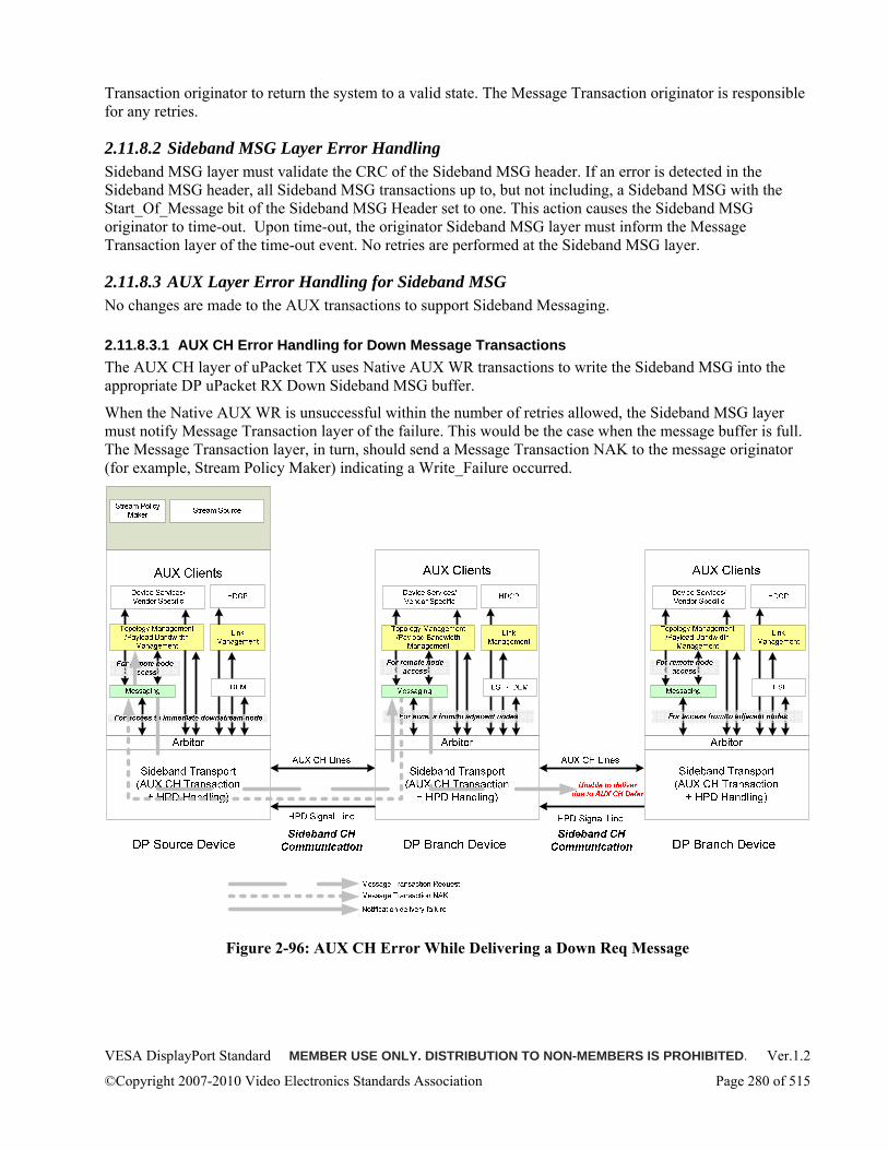
VESA DisplayPort Standard MEMBER USE ONLY. DISTRIBUTION TO NON-MEMBERS IS PROHIBITED. Ver.1.2
©Copyright 2007-2010 Video Electronics Standards Association Page 280 of 515
Transaction originator to return the system to a valid state. The Message Transaction originator is responsible for any retries.
2.11.8.2 Sideband MSG Layer Error Handling Sideband MSG layer must validate the CRC of the Sideband MSG header. If an error is detected in the Sideband MSG header, all Sideband MSG transactions up to, but not including, a Sideband MSG with the Start_Of_Message bit of the Sideband MSG Header set to one. This action causes the Sideband MSG originator to time-out. Upon time-out, the originator Sideband MSG layer must inform the Message Transaction layer of the time-out event. No retries are performed at the Sideband MSG layer.
2.11.8.3 AUX Layer Error Handling for Sideband MSG No changes are made to the AUX transactions to support Sideband Messaging.
2.11.8.3.1 AUX CH Error Handling for Down Message Transactions The AUX CH layer of uPacket TX uses Native AUX WR transactions to write the Sideband MSG into the appropriate DP uPacket RX Down Sideband MSG buffer.
When the Native AUX WR is unsuccessful within the number of retries allowed, the Sideband MSG layer must notify Message Transaction layer of the failure. This would be the case when the message buffer is full. The Message Transaction layer, in turn, should send a Message Transaction NAK to the message originator (for example, Stream Policy Maker) indicating a Write_Failure occurred.
Figure 2-96: AUX CH Error While Delivering a Down Req Message
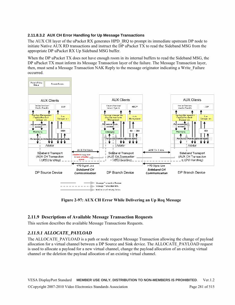
VESA DisplayPort Standard MEMBER USE ONLY. DISTRIBUTION TO NON-MEMBERS IS PROHIBITED. Ver.1.2
©Copyright 2007-2010 Video Electronics Standards Association Page 281 of 515
2.11.8.3.2 AUX CH Error Handling for Up Message Transactions The AUX CH layer of the uPacket RX generates HPD_IRQ to prompt its immediate upstream DP node to initiate Native AUX RD transactions and instruct the DP uPacket TX to read the Sideband MSG from the appropriate DP uPacket RX Up Sideband MSG buffer.
When the DP uPacket TX does not have enough room in its internal buffers to read the Sideband MSG, the DP uPacket TX must inform its Message Transaction layer of the failure. The Message Transaction layer, then, must send a Message Transaction NAK Reply to the message originator indicating a Write_Failure occurred.
Figure 2-97: AUX CH Error While Delivering an Up Req Message
2.11.9 Descriptions of Available Message Transaction Requests This section describes the available Message Transactions Requests.
2.11.9.1 ALLOCATE_PAYLOAD The ALLOCATE_PAYLOAD is a path or node request Message Transaction allowing the change of payload allocation for a virtual channel between a DP Source and Sink device. The ALLOCATE_PAYLOAD request is used to allocate a payload for a new virtual channel, change the payload allocation of an existing virtual channel or the deletion the payload allocation of an existing virtual channel.
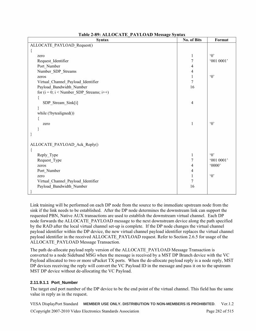
VESA DisplayPort Standard MEMBER USE ONLY. DISTRIBUTION TO NON-MEMBERS IS PROHIBITED. Ver.1.2
©Copyright 2007-2010 Video Electronics Standards Association Page 282 of 515
Table 2-89: ALLOCATE_PAYLOAD Message Syntax Syntax No. of Bits Format
ALLOCATE_PAYLOAD_Request() zero Request_Identifier Port_Number Number_SDP_Streams zeros Virtual_Channel_Payload_Identifier Payload_Bandwidth_Number for (i = 0; i < Number_SDP_Streams; i++) SDP_Stream_Sink[i] while (!bytealigned()) zero ALLOCATE_PAYLOAD_Ack_Reply() Reply_Type Request_Type zeros Port_Number zero Virtual_Channel_Payload_Identifier Payload_Bandwidth_Number
1 7 4 4 1 7
16
4
1
1 7 4 4 1 7
16
‘0’ ‘001 0001’
‘0’ ‘0’ ‘0’ ‘001 0001’ ‘0000’ ‘0’
Link training will be performed on each DP node from the source to the immediate upstream node from the sink if the link needs to be established. After the DP node determines the downstream link can support the requested PBN, Native AUX transactions are used to establish the downstream virtual channel. Each DP node forwards the ALLOCATE_PAYLOAD message to the next downstream device along the path specified by the RAD after the local virtual channel set-up is complete. If the DP node changes the virtual channel payload identifier within the DP device, the new virtual channel payload identifier replaces the virtual channel payload identifier in the received ALLOCATE_PAYLOAD request. Refer to Section 2.6.5 for usage of the ALLOCATE_PAYLOAD Message Transaction.
The path de-allocate payload reply version of the ALLOCATE_PAYLOAD Message Transaction is converted to a node Sideband MSG when the message is received by a MST DP Branch device with the VC Payload allocated to two or more uPacket TX ports. When the de-allocate payload reply is a node reply, MST DP devices receiving the reply will convert the VC Payload ID in the message and pass it on to the upstream MST DP device without de-allocating the VC Payload.
2.11.9.1.1 Port_Number The target end port number of the DP device to be the end point of the virtual channel. This field has the same value in reply as in the request.
VESA DisplayPort Standard MEMBER USE ONLY. DISTRIBUTION TO NON-MEMBERS IS PROHIBITED. Ver.1.2
©Copyright 2007-2010 Video Electronics Standards Association Page 283 of 515
2.11.9.1.2 Virtual_Channel_Payload_Identifier The virtual channel payload identifier of the virtual channel to be added, updated or deleted. This field has the same value in reply as in the request.
2.11.9.1.3 Payload_Bandwidth_Number The Payload Bandwidth Number required for the virtual channel assigned the above virtual channel identifier. This field has the same value in reply as in the request.
2.11.9.1.4 Number_SDP_Streams The Number_SDP_Streams field indicates the number of SDP streams which need to be routed to SDP stream sinks (the size of the SDP stream sink table which follows).
2.11.9.1.5 SDP_Stream_Sink The SDP Stream Sink table contains the mapping of the SDP stream to the available SDP stream sinks. The first field of the table is associated with the first SDP stream, the second field the second SDP stream and so forth. The value of each field in the table is the SDP stream sink identifier the associated SDP stream being sent to. When the SDP_Stream_Sink value is set to zero, the destination SDP Sink device the SDP stream is sent is implementation-specific. It is the decision of the DP Sink device implementer as to how to handle two SDP streams assigned to the same SDP stream sink.
2.11.9.2 CLEAR_PAYLOAD_ID_TABLE The CLEAR_PAYLOAD_ID_TABLE path broadcast request message transaction is sent by a MST DP device to de-allocate all VC Payload Id. tables allocated to the port the message is received from. This broadcast message is not sent to all downstream ports. The broadcast message is sent to those uPacket TX ports with VC Payloads allocated from the uPacket RX port being cleared. When the CLEAR_PAYLOAD_ID_TABLE request is received by a concentrator device, the MST DP Concentrator Branch device sends a NAK reply with the reason set to defer.
The MST DP Concentrator Branch device, ACKs CLEAR_PAYLOAD_ID_TABLE broadcast request message transactions, and converts the CLEAR_PAYLOAD_ID_TABLE request into a series of ALLOCATE_PAYLOAD requests for the VC Payload ID allocated to the uPacket RX port with the new PBN value set to zero (de-allocate payload) to its downstream uPacket TX ports.
Table 2-90: CLEAR_PAYLOAD_ID_TABLE Message Syntax Syntax No. of Bits Format
CLEAR_PAYLOAD_ID_TABLE_Request() zero Request_Identifier CLEAR_PAYLOAD_ID_TABLE_Ack_Reply() Reply_Type Request_Type
1 7
1 7
‘0’ ‘000 0100’ ‘0’ ‘000 0100’
2.11.9.3 CONNECTION_STATUS_NOTIFY The CONNECTION_STATUS_NOTIFY node broadcast request message transaction is sent by a DP branch device when it detects a DP or legacy device plug or unplug event. The MST device whose uPacket TX detected the connection status change will broadcast the message upstream, while the MST device whose
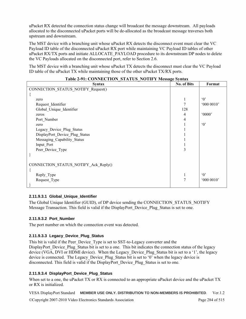
VESA DisplayPort Standard MEMBER USE ONLY. DISTRIBUTION TO NON-MEMBERS IS PROHIBITED. Ver.1.2
©Copyright 2007-2010 Video Electronics Standards Association Page 284 of 515
uPacket RX detected the connection status change will broadcast the message downstream. All payloads allocated to the disconnected uPacket ports will be de-allocated as the broadcast message traverses both upstream and downstream.
The MST device with a branching unit whose uPacket RX detects the disconnect event must clear the VC Payload ID table of the disconnected uPacket RX port while maintaining VC Payload ID tables of other uPacket RX/TX ports and initiate ALLOCATE_PAYLOAD procedure to its downstream DP nodes to delete the VC Payloads allocated on the disconnected port, refer to Section 2.6.
The MST device with a branching unit whose uPacket TX detects the disconnect must clear the VC Payload ID table of the uPacket TX while maintaining those of the other uPacket TX/RX ports.
Table 2-91: CONNECTION_STATUS_NOTIFY Message Syntax Syntax No. of Bits Format
CONNECTION_STATUS_NOTIFY_Request() zero Request_Identifier Global_Unique_Identifier zeros Port_Number zero Legacy_Device_Plug_Status DisplayPort_Device_Plug_Status Messaging_Capability_Status Input_Port Peer_Device_Type CONNECTION_STATUS_NOTIFY_Ack_Reply() Reply_Type Request_Type
1 7
128 4 4 1 1 1 1 1 3
1 7
‘0’ ‘000 0010’ ‘0000’ ‘0’ ‘0’ ‘000 0010’
2.11.9.3.1 Global_Unique_Identifier The Global Unique Identifier (GUID), of DP device sending the CONNECTION_STATUS_NOTIFY Message Transaction. This field is valid if the DisplayPort_Device_Plug_Status is set to one.
2.11.9.3.2 Port_Number The port number on which the connection event was detected.
2.11.9.3.3 Legacy_Device_Plug_Status This bit is valid if the Peer_Device_Type is set to SST-to-Legacy converter and the DisplayPort_Device_Plug_Status bit is set to a one. This bit indicates the connection status of the legacy device (VGA, DVI or HDMI device). When the Legacy_Device_Plug_Status bit is set to a ‘1’, the legacy device is connected. The Legacy_Device_Plug_Status bit is set to ‘0’ when the legacy device is disconnected. This field is valid if the DisplayPort_Device_Plug_Status is set to one.
2.11.9.3.4 DisplayPort_Device_Plug_Status When set to a one, the uPacket TX or RX is connected to an appropriate uPacket device and the uPacket TX or RX is initialized.
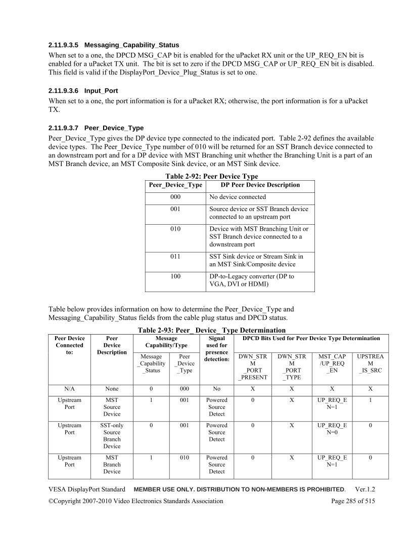
VESA DisplayPort Standard MEMBER USE ONLY. DISTRIBUTION TO NON-MEMBERS IS PROHIBITED. Ver.1.2
©Copyright 2007-2010 Video Electronics Standards Association Page 285 of 515
2.11.9.3.5 Messaging_Capability_Status When set to a one, the DPCD MSG_CAP bit is enabled for the uPacket RX unit or the UP_REQ_EN bit is enabled for a uPacket TX unit. The bit is set to zero if the DPCD MSG_CAP or UP_REQ_EN bit is disabled. This field is valid if the DisplayPort_Device_Plug_Status is set to one.
2.11.9.3.6 Input_Port When set to a one, the port information is for a uPacket RX; otherwise, the port information is for a uPacket TX.
2.11.9.3.7 Peer_Device_Type Peer_Device_Type gives the DP device type connected to the indicated port. Table 2-92 defines the available device types. The Peer_Device_Type number of 010 will be returned for an SST Branch device connected to an downstream port and for a DP device with MST Branching unit whether the Branching Unit is a part of an MST Branch device, an MST Composite Sink device, or an MST Sink device.
Table 2-92: Peer Device Type
Table below provides information on how to determine the Peer_Device_Type and Messaging_Capability_Status fields from the cable plug status and DPCD status.
Table 2-93: Peer_ Device_ Type Determination Message
Capability/Type DPCD Bits Used for Peer Device Type Determination Peer Device
Connected to:
Peer Device
Description Message
_Capability_Status
Peer _Device_Type
Signal used for presence detection: DWN_STR
M _PORT
_PRESENT
DWN_STRM
_PORT _TYPE
MST_CAP /UP_REQ
_EN
UPSTREAM
_IS_SRC
N/A None 0 000 No X X X X
Upstream Port
MST Source Device
1 001 Powered Source Detect
0 X UP_REQ_EN=1
1
Upstream Port
SST-only Source Branch Device
0 001 Powered Source Detect
0 X UP_REQ_EN=0
0
Upstream Port
MST Branch Device
1 010 Powered Source Detect
0 X UP_REQ_EN=1
0
Peer_Device_Type DP Peer Device Description
000 No device connected
001 Source device or SST Branch device connected to an upstream port
010 Device with MST Branching Unit or SST Branch device connected to a downstream port
011 SST Sink device or Stream Sink in an MST Sink/Composite device
100 DP-to-Legacy converter (DP to VGA, DVI or HDMI)
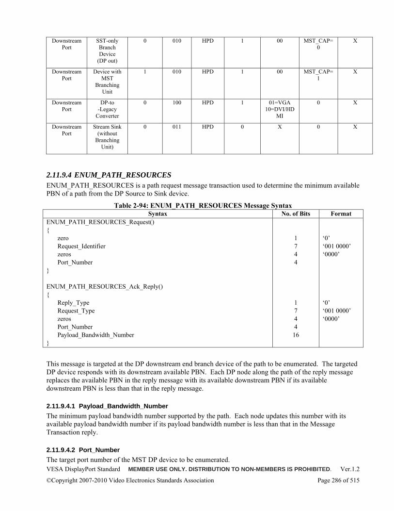
VESA DisplayPort Standard MEMBER USE ONLY. DISTRIBUTION TO NON-MEMBERS IS PROHIBITED. Ver.1.2
©Copyright 2007-2010 Video Electronics Standards Association Page 286 of 515
Downstream Port
SST-only Branch Device
(DP out)
0 010 HPD 1 00 MST_CAP=0
X
Downstream Port
Device with MST
Branching Unit
1 010 HPD 1 00 MST_CAP=1
X
Downstream Port
DP-to -Legacy
Converter
0 100 HPD 1 01=VGA 10=DVI/HD
MI
0 X
Downstream Port
Stream Sink (without
Branching Unit)
0 011 HPD 0 X 0 X
2.11.9.4 ENUM_PATH_RESOURCES ENUM_PATH_RESOURCES is a path request message transaction used to determine the minimum available PBN of a path from the DP Source to Sink device.
Table 2-94: ENUM_PATH_RESOURCES Message Syntax Syntax No. of Bits Format
ENUM_PATH_RESOURCES_Request() zero Request_Identifier zeros Port_Number ENUM_PATH_RESOURCES_Ack_Reply() Reply_Type Request_Type zeros Port_Number Payload_Bandwidth_Number
1 7 4 4
1 7 4 4
16
‘0’ ‘001 0000’ ‘0000’ ‘0’ ‘001 0000’ ‘0000’
This message is targeted at the DP downstream end branch device of the path to be enumerated. The targeted DP device responds with its downstream available PBN. Each DP node along the path of the reply message replaces the available PBN in the reply message with its available downstream PBN if its available downstream PBN is less than that in the reply message.
2.11.9.4.1 Payload_Bandwidth_Number The minimum payload bandwidth number supported by the path. Each node updates this number with its available payload bandwidth number if its payload bandwidth number is less than that in the Message Transaction reply.
2.11.9.4.2 Port_Number The target port number of the MST DP device to be enumerated.
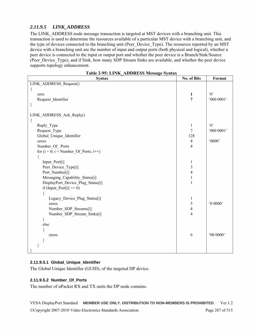
VESA DisplayPort Standard MEMBER USE ONLY. DISTRIBUTION TO NON-MEMBERS IS PROHIBITED. Ver.1.2
©Copyright 2007-2010 Video Electronics Standards Association Page 287 of 515
2.11.9.5 LINK_ADDRESS The LINK_ADDRESS node message transaction is targeted at MST devices with a branching unit. This transaction is used to determine the resources available of a particular MST device with a branching unit, and the type of devices connected to the branching unit (Peer_Device_Type). The resources reported by an MST device with a branching unit are the number of input and output ports (both physical and logical), whether a peer device is connected to the input or output port and whether the peer device is a Branch/Sink/Source (Peer_Device_Type), and if Sink, how many SDP Stream Sinks are available, and whether the peer device supports topology enhancement.
Table 2-95: LINK_ADDRESS Message Syntax Syntax No. of Bits Format
LINK_ADDRESS_Request() zero Request_Identifier LINK_ADDRESS_Ack_Reply() Reply_Type Request_Type Global_Unique_Identifier zeros Number_Of_ Ports for (i = 0; i < Number_Of_Ports; i++) Input_Port[i] Peer_Device_Type[i] Port_Number[i] Messaging_Capability_Status[i] DisplayPort_Device_Plug_Status[i] if (Input_Port[i] == 0) Legacy_Device_Plug_Status[i] zeros Number_SDP_Streams[i] Number_SDP_Stream_Sinks[i] else zeros
1 7
1 7
128 4 4
1 3 4 1 1
1 5 4 4
6
‘0’ ‘000 0001’ ‘0’ ‘000 0001’ ‘0000’ ‘0 0000’ ’00 0000’
2.11.9.5.1 Global_Unique_Identifier The Global Unique Identifier (GUID), of the targeted DP device.
2.11.9.5.2 Number_Of_Ports The number of uPacket RX and TX units the DP node contains.
VESA DisplayPort Standard MEMBER USE ONLY. DISTRIBUTION TO NON-MEMBERS IS PROHIBITED. Ver.1.2
©Copyright 2007-2010 Video Electronics Standards Association Page 288 of 515
2.11.9.5.3 Input_Port When set to a one the port information is for a uPacket RX. Otherwise, port information is for a uPacket TX.
2.11.9.5.4 Peer_Device_Type Per_Device_Type gives the DP device type connected to the indicated port. Table 2-92 gives the defined peer device types. The DP Peer Branch Device type will be returned for all branch types, physical, logical or combined. This field is valid if the DisplayPort_Device_Plug_Status is set to one.
2.11.9.5.5 Port_Number The port number of the port being reported. Physical port numbers will be from zero to seven while logical port numbers will be from eight to 15 (0x0F).
2.11.9.5.6 Messaging_Capability_Status When set to a one, the DPCD MSG_CAP bit is enabled for the uPacket RX unit or the UP_REQ_EN bit is enabled for a uPacket TX unit. The bit is set to zero if the DPCD MSG_CAP or UP_REQ_EN bit is disabled. This field is valid if the DisplayPort_Device_Plug_Status is set to one.
2.11.9.5.7 DisplayPort_Device_Plug_Status When set to a one, the uPacket TX or RX is connected to an appropriate uPacket unit and the uPacket TX or RX is initialized.
2.11.9.5.8 Legacy_Device_Plug_Status This bit is valid if the Peer_Device_Type is set to SST-to-Legacy converter. This bit indicates the connection status of the legacy device (VGA, DVI or HDMI device). When the Legacy_Device_Plug_Status bit is set to a ‘1’, the legacy device is connected. The Legacy_Device_Plug_Status bit is set to ‘0’ when the legacy device is disconnected. This field is valid if the DisplayPort_Device_Plug_Status is set to one.
2.11.9.5.9 Number_SDP_Streams The Number_SDP_Streams field reports the number of SDP streams the DP port can simultaneously handle. This field is valid if the DisplayPort_Device_Plug_Status is set to one.
2.11.9.5.10 Number_SDP_Stream_Sinks The Number_SDP_Stream_Sinks field reports the number of SDP stream sinks associated with the DP port. This field is valid if the DisplayPort_Device_Plug_Status is set to one.
2.11.9.6 POWER_DOWN_PHY POWER_DOWN_PHY request is a path or node request message transaction.
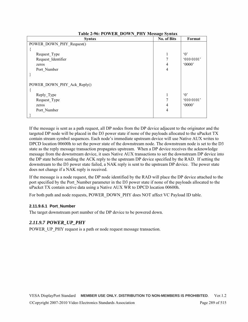
VESA DisplayPort Standard MEMBER USE ONLY. DISTRIBUTION TO NON-MEMBERS IS PROHIBITED. Ver.1.2
©Copyright 2007-2010 Video Electronics Standards Association Page 289 of 515
Table 2-96: POWER_DOWN_PHY Message Syntax Syntax No. of Bits Format
POWER_DOWN_PHY_Request() Request_Type Request_Identifier zeros Port_Number POWER_DOWN_PHY_Ack_Reply() Reply_Type Request_Type zeros Port_Number
1 7 4 4
1 7 4 4
‘0’ ‘010 0101’ ‘0000’ ‘0’ ‘010 0101’ ‘0000’
If the message is sent as a path request, all DP nodes from the DP device adjacent to the originator and the targeted DP node will be placed in the D3 power state if none of the payloads allocated to the uPacket TX contain stream symbol sequences. Each node’s immediate upstream device will use Native AUX writes to DPCD location 00600h to set the power state of the downstream node. The downstream node is set to the D3 state as the reply message transaction propagates upstream. When a DP device receives the acknowledge message from the downstream device, it uses Native AUX transactions to set the downstream DP device into the DP state before sending the ACK reply to the upstream DP device specified by the RAD. If setting the downstream to the D3 power state failed, a NAK reply is sent to the upstream DP device. The power state does not change if a NAK reply is received.
If the message is a node request, the DP node identified by the RAD will place the DP device attached to the port specified by the Port_Number parameter in the D3 power state if none of the payloads allocated to the uPacket TX contain active data using a Native AUX WR to DPCD location 00600h.
For both path and node requests, POWER_DOWN_PHY does NOT affect VC Payload ID table.
2.11.9.6.1 Port_Number The target downstream port number of the DP device to be powered down.
2.11.9.7 POWER_UP_PHY POWER_UP_PHY request is a path or node request message transaction.
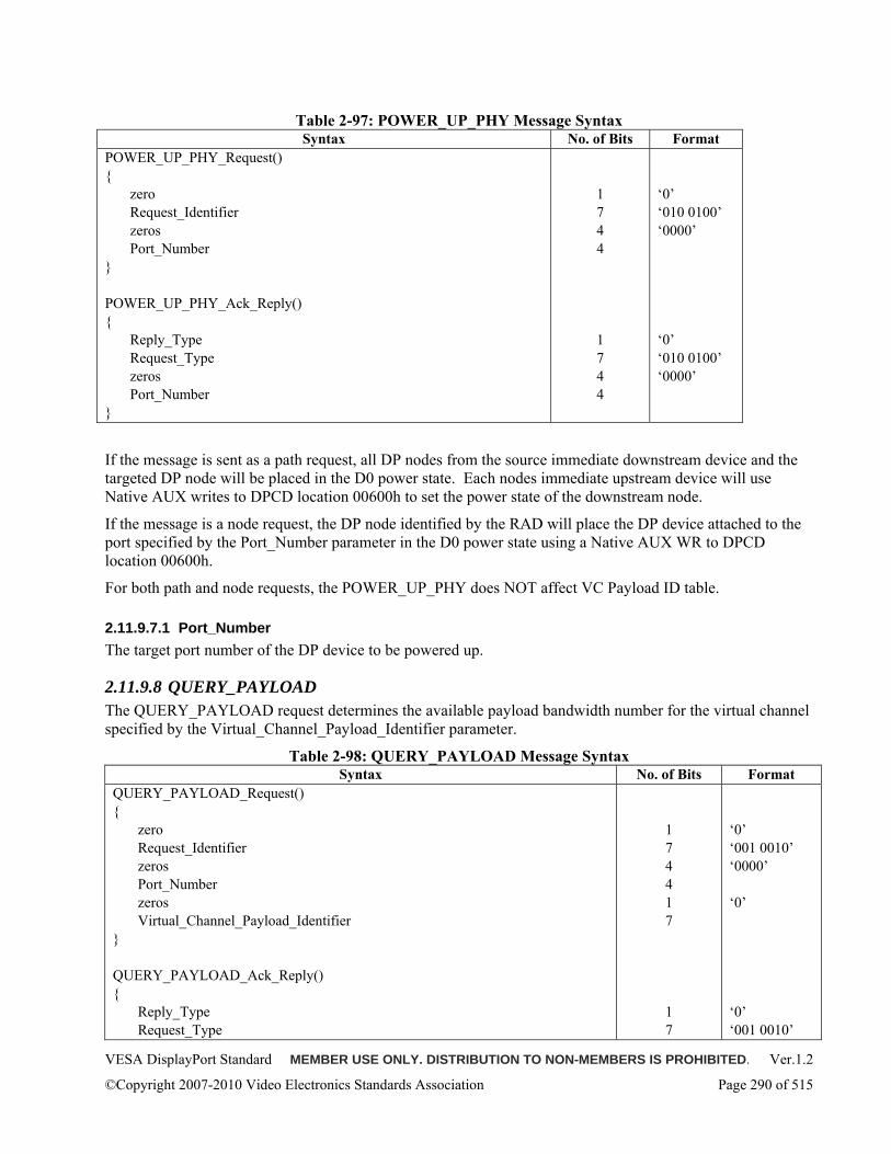
VESA DisplayPort Standard MEMBER USE ONLY. DISTRIBUTION TO NON-MEMBERS IS PROHIBITED. Ver.1.2
©Copyright 2007-2010 Video Electronics Standards Association Page 290 of 515
Table 2-97: POWER_UP_PHY Message Syntax Syntax No. of Bits Format
POWER_UP_PHY_Request() zero Request_Identifier zeros Port_Number POWER_UP_PHY_Ack_Reply() Reply_Type Request_Type zeros Port_Number
1 7 4 4
1 7 4 4
‘0’ ‘010 0100’ ‘0000’ ‘0’ ‘010 0100’ ‘0000’
If the message is sent as a path request, all DP nodes from the source immediate downstream device and the targeted DP node will be placed in the D0 power state. Each nodes immediate upstream device will use Native AUX writes to DPCD location 00600h to set the power state of the downstream node.
If the message is a node request, the DP node identified by the RAD will place the DP device attached to the port specified by the Port_Number parameter in the D0 power state using a Native AUX WR to DPCD location 00600h.
For both path and node requests, the POWER_UP_PHY does NOT affect VC Payload ID table.
2.11.9.7.1 Port_Number The target port number of the DP device to be powered up.
2.11.9.8 QUERY_PAYLOAD The QUERY_PAYLOAD request determines the available payload bandwidth number for the virtual channel specified by the Virtual_Channel_Payload_Identifier parameter.
Table 2-98: QUERY_PAYLOAD Message Syntax Syntax No. of Bits Format
QUERY_PAYLOAD_Request() zero Request_Identifier zeros Port_Number zeros Virtual_Channel_Payload_Identifier QUERY_PAYLOAD_Ack_Reply() Reply_Type Request_Type
1 7 4 4 1 7
1 7
‘0’ ‘001 0010’ ‘0000’ ‘0’ ‘0’ ‘001 0010’
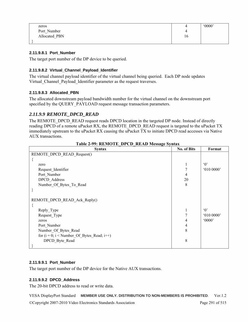
VESA DisplayPort Standard MEMBER USE ONLY. DISTRIBUTION TO NON-MEMBERS IS PROHIBITED. Ver.1.2
©Copyright 2007-2010 Video Electronics Standards Association Page 291 of 515
zeros Port_Number Allocated_PBN
4 4
16
‘0000’
2.11.9.8.1 Port_Number The target port number of the DP device to be queried.
2.11.9.8.2 Virtual_Channel_Payload_Identifier The virtual channel payload identifier of the virtual channel being queried. Each DP node updates Virtual_Channel_Payload_Identifier parameter as the request traverses.
2.11.9.8.3 Allocated_PBN The allocated downstream payload bandwidth number for the virtual channel on the downstream port specified by the QUERY_PAYLOAD request message transaction parameters.
2.11.9.9 REMOTE_DPCD_READ The REMOTE_DPCD_READ request reads DPCD location in the targeted DP node. Instead of directly reading DPCD of a remote uPacket RX, the REMOTE_DPCD_READ request is targeted to the uPacket TX immediately upstream to the uPacket RX causing the uPacket TX to initiate DPCD read accesses via Native AUX transactions.
Table 2-99: REMOTE_DPCD_READ Message Syntax Syntax No. of Bits Format
REMOTE_DPCD_READ_Request() zero Request_Identifier Port_Number DPCD_Address Number_Of_Bytes_To_Read REMOTE_DPCD_READ_Ack_Reply() Reply_Type Request_Type zeros Port_Number Number_Of_Bytes_Read for (i = 0; i < Number_Of_Bytes_Read; i++) DPCD_Byte_Read
1 7 4
20 8
1 7 4 4 8
8
‘0’ ‘010 0000’ ‘0’ ‘010 0000’ ‘0000’
2.11.9.9.1 Port_Number The target port number of the DP device for the Native AUX transactions.
2.11.9.9.2 DPCD_Address The 20-bit DPCD address to read or write data.
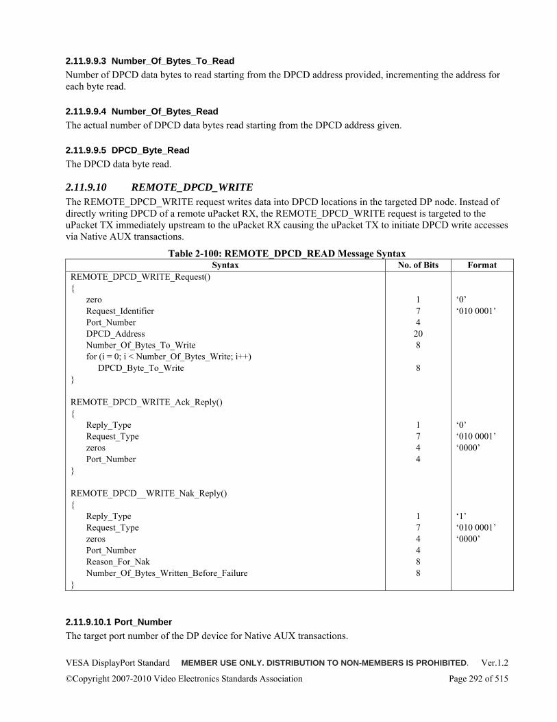
VESA DisplayPort Standard MEMBER USE ONLY. DISTRIBUTION TO NON-MEMBERS IS PROHIBITED. Ver.1.2
©Copyright 2007-2010 Video Electronics Standards Association Page 292 of 515
2.11.9.9.3 Number_Of_Bytes_To_Read Number of DPCD data bytes to read starting from the DPCD address provided, incrementing the address for each byte read.
2.11.9.9.4 Number_Of_Bytes_Read The actual number of DPCD data bytes read starting from the DPCD address given.
2.11.9.9.5 DPCD_Byte_Read The DPCD data byte read.
2.11.9.10 REMOTE_DPCD_WRITE The REMOTE_DPCD_WRITE request writes data into DPCD locations in the targeted DP node. Instead of directly writing DPCD of a remote uPacket RX, the REMOTE_DPCD_WRITE request is targeted to the uPacket TX immediately upstream to the uPacket RX causing the uPacket TX to initiate DPCD write accesses via Native AUX transactions.
Table 2-100: REMOTE_DPCD_READ Message Syntax Syntax No. of Bits Format
REMOTE_DPCD_WRITE_Request() zero Request_Identifier Port_Number DPCD_Address Number_Of_Bytes_To_Write for (i = 0; i < Number_Of_Bytes_Write; i++) DPCD_Byte_To_Write REMOTE_DPCD_WRITE_Ack_Reply() Reply_Type Request_Type zeros Port_Number REMOTE_DPCD__WRITE_Nak_Reply() Reply_Type Request_Type zeros Port_Number Reason_For_Nak Number_Of_Bytes_Written_Before_Failure
1 7 4
20 8
8
1 7 4 4
1 7 4 4 8 8
‘0’ ‘010 0001’ ‘0’ ‘010 0001’ ‘0000’ ‘1’ ‘010 0001’ ‘0000’
2.11.9.10.1 Port_Number The target port number of the DP device for Native AUX transactions.
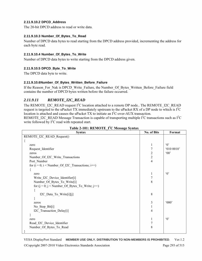
VESA DisplayPort Standard MEMBER USE ONLY. DISTRIBUTION TO NON-MEMBERS IS PROHIBITED. Ver.1.2
©Copyright 2007-2010 Video Electronics Standards Association Page 293 of 515
2.11.9.10.2 DPCD_Address The 20-bit DPCD address to read or write data.
2.11.9.10.3 Number_Of_Bytes_To_Read Number of DPCD data bytes to read starting from the DPCD address provided, incrementing the address for each byte read.
2.11.9.10.4 Number_Of_Bytes_To_Write Number of DPCD data bytes to write starting from the DPCD address given.
2.11.9.10.5 DPCD_Byte_To_Write The DPCD data byte to write.
2.11.9.10.6 Number_Of_Bytes_Written_Before_Failure If the Reason_For_Nak is DPCD_Write_Failure, the Number_Of_Bytes_Written_Before_Failure field contains the number of DPCD bytes written before the failure occurred.
2.11.9.11 REMOTE_I2C_READ The REMOTE_I2C_READ request I2C location attached to a remote DP node.. The REMOTE_I2C_READ request is targeted to the uPacket TX immediately upstream to the uPacket RX of a DP node to which is I2C location is attached and causes the uPacket TX to initiate an I2C-over-AUX transaction. REMOTE_I2C_READ Message Transaction is capable of transporting multiple I2C transactions such as I2C write followed by I2C read with repeated start.
Table 2-101: REMOTE_I2C Message Syntax Syntax No. of Bits Format
REMOTE_I2C_READ_Request() zero Request_Identifier zeros Number_Of_I2C_Write_Transactions Port_Number for (i = 0; i < Number_Of_I2C_Transactions; i++) zero Write_I2C_Device_Identifier[i] Number_Of_Bytes_To_Write[i] for (j = 0; j < Number_Of_Bytes_To_Write; j++) I2C_Data_To_Write[i][j] zeros No_Stop_Bit[i] I2C_Transaction_Delay[i] zero Read_I2C_Device_Identifier Number_Of_Bytes_To_Read
1 7 2 2 4
1 7 8
8
3 1 4
1 7 8
‘0’ ‘010 0010’ ‘00’ ‘0’ ‘000’ ‘0’
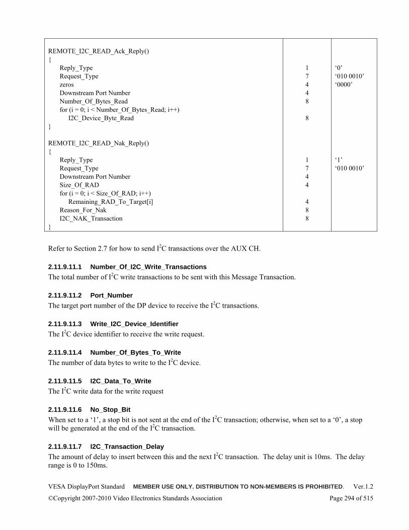
VESA DisplayPort Standard MEMBER USE ONLY. DISTRIBUTION TO NON-MEMBERS IS PROHIBITED. Ver.1.2
©Copyright 2007-2010 Video Electronics Standards Association Page 294 of 515
REMOTE_I2C_READ_Ack_Reply() Reply_Type Request_Type zeros Downstream Port Number Number_Of_Bytes_Read for (i = 0; i < Number_Of_Bytes_Read; i++) I2C_Device_Byte_Read REMOTE_I2C_READ_Nak_Reply() Reply_Type Request_Type Downstream Port Number Size_Of_RAD for (i = 0; i < Size_Of_RAD; i++) Remaining_RAD_To_Target[i] Reason_For_Nak I2C_NAK_Transaction
1 7 4 4 8
8
1 7 4 4
4 8 8
‘0’ ‘010 0010’ ‘0000’ ‘1’ ‘010 0010’
Refer to Section 2.7 for how to send I2C transactions over the AUX CH.
2.11.9.11.1 Number_Of_I2C_Write_Transactions The total number of I2C write transactions to be sent with this Message Transaction.
2.11.9.11.2 Port_Number The target port number of the DP device to receive the I2C transactions.
2.11.9.11.3 Write_I2C_Device_Identifier The I2C device identifier to receive the write request.
2.11.9.11.4 Number_Of_Bytes_To_Write The number of data bytes to write to the I2C device.
2.11.9.11.5 I2C_Data_To_Write The I2C write data for the write request
2.11.9.11.6 No_Stop_Bit When set to a ‘1’, a stop bit is not sent at the end of the I2C transaction; otherwise, when set to a ‘0’, a stop will be generated at the end of the I2C transaction.
2.11.9.11.7 I2C_Transaction_Delay The amount of delay to insert between this and the next I2C transaction. The delay unit is 10ms. The delay range is 0 to 150ms.
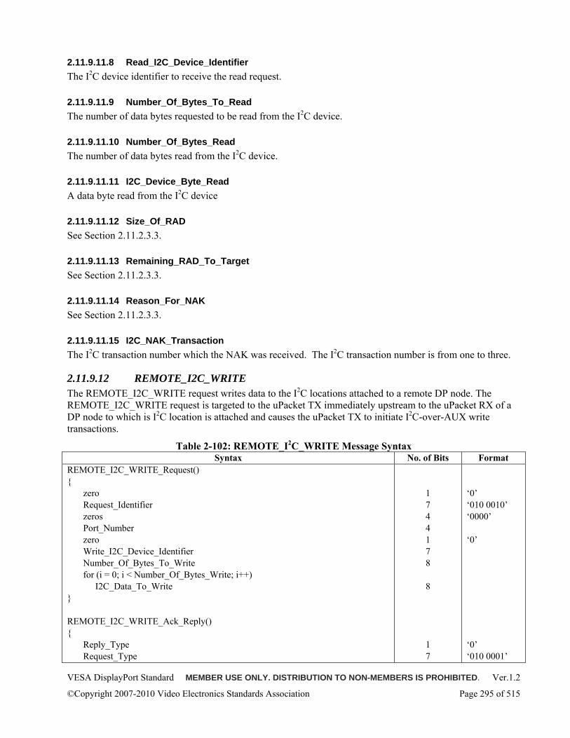
VESA DisplayPort Standard MEMBER USE ONLY. DISTRIBUTION TO NON-MEMBERS IS PROHIBITED. Ver.1.2
©Copyright 2007-2010 Video Electronics Standards Association Page 295 of 515
2.11.9.11.8 Read_I2C_Device_Identifier The I2C device identifier to receive the read request.
2.11.9.11.9 Number_Of_Bytes_To_Read The number of data bytes requested to be read from the I2C device.
2.11.9.11.10 Number_Of_Bytes_Read The number of data bytes read from the I2C device.
2.11.9.11.11 I2C_Device_Byte_Read A data byte read from the I2C device
2.11.9.11.12 Size_Of_RAD See Section 2.11.2.3.3.
2.11.9.11.13 Remaining_RAD_To_Target See Section 2.11.2.3.3.
2.11.9.11.14 Reason_For_NAK See Section 2.11.2.3.3.
2.11.9.11.15 I2C_NAK_Transaction The I2C transaction number which the NAK was received. The I2C transaction number is from one to three.
2.11.9.12 REMOTE_I2C_WRITE The REMOTE_I2C_WRITE request writes data to the I2C locations attached to a remote DP node. The REMOTE_I2C_WRITE request is targeted to the uPacket TX immediately upstream to the uPacket RX of a DP node to which is I2C location is attached and causes the uPacket TX to initiate I2C-over-AUX write transactions.
Table 2-102: REMOTE_I2C_WRITE Message Syntax Syntax No. of Bits Format
REMOTE_I2C_WRITE_Request() zero Request_Identifier zeros Port_Number zero Write_I2C_Device_Identifier Number_Of_Bytes_To_Write for (i = 0; i < Number_Of_Bytes_Write; i++) I2C_Data_To_Write REMOTE_I2C_WRITE_Ack_Reply() Reply_Type Request_Type
1 7 4 4 1 7 8
8
1 7
‘0’ ‘010 0010’ ‘0000’ ‘0’ ‘0’ ‘010 0001’
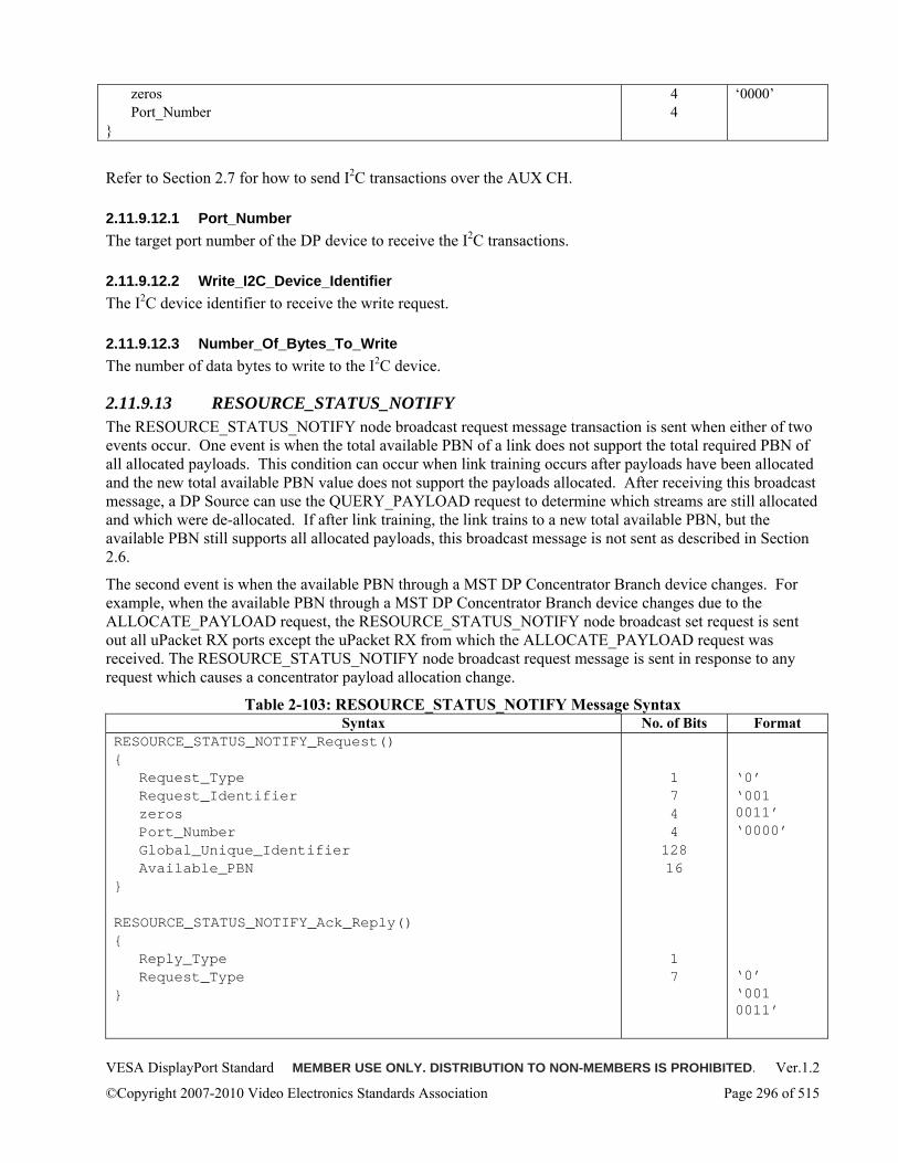
VESA DisplayPort Standard MEMBER USE ONLY. DISTRIBUTION TO NON-MEMBERS IS PROHIBITED. Ver.1.2
©Copyright 2007-2010 Video Electronics Standards Association Page 296 of 515
zeros Port_Number
4 4
‘0000’
Refer to Section 2.7 for how to send I2C transactions over the AUX CH.
2.11.9.12.1 Port_Number The target port number of the DP device to receive the I2C transactions.
2.11.9.12.2 Write_I2C_Device_Identifier The I2C device identifier to receive the write request.
2.11.9.12.3 Number_Of_Bytes_To_Write The number of data bytes to write to the I2C device.
2.11.9.13 RESOURCE_STATUS_NOTIFY The RESOURCE_STATUS_NOTIFY node broadcast request message transaction is sent when either of two events occur. One event is when the total available PBN of a link does not support the total required PBN of all allocated payloads. This condition can occur when link training occurs after payloads have been allocated and the new total available PBN value does not support the payloads allocated. After receiving this broadcast message, a DP Source can use the QUERY_PAYLOAD request to determine which streams are still allocated and which were de-allocated. If after link training, the link trains to a new total available PBN, but the available PBN still supports all allocated payloads, this broadcast message is not sent as described in Section 2.6.
The second event is when the available PBN through a MST DP Concentrator Branch device changes. For example, when the available PBN through a MST DP Concentrator Branch device changes due to the ALLOCATE_PAYLOAD request, the RESOURCE_STATUS_NOTIFY node broadcast set request is sent out all uPacket RX ports except the uPacket RX from which the ALLOCATE_PAYLOAD request was received. The RESOURCE_STATUS_NOTIFY node broadcast request message is sent in response to any request which causes a concentrator payload allocation change.
Table 2-103: RESOURCE_STATUS_NOTIFY Message Syntax Syntax No. of Bits Format
RESOURCE_STATUS_NOTIFY_Request() Request_Type Request_Identifier zeros Port_Number Global_Unique_Identifier Available_PBN RESOURCE_STATUS_NOTIFY_Ack_Reply() Reply_Type Request_Type
1 7 4 4 128 16 1 7
‘0’ ‘001 0011’ ‘0000’ ‘0’ ‘001 0011’
VESA DisplayPort Standard MEMBER USE ONLY. DISTRIBUTION TO NON-MEMBERS IS PROHIBITED. Ver.1.2
©Copyright 2007-2010 Video Electronics Standards Association Page 297 of 515
2.11.9.13.1 Global_Unique_Identifier The Global Unique Identifier (GUID), of DP device reporting resource change.
2.11.9.13.2 Port_Number uPacket TX port number of resource change.
2.11.9.13.3 Avaliable_PBN The newly available PBN for the port where resource allocation changed.
2.11.9.14 SINK_EVENT_NOTIFY SINK_EVENT_NOTIFY is an upward-going Broadcast Message Transaction. For example, a change to a Sink device (for example, a display) induced by an end user action via OSD button and menu is to be communicated to a Source device (for example, PC graphics) via SINK_EVENT_NOTIFY Broadcast Message Transaction. The syntax is to be defined in the future revision of this standard.
2.11.9.15 QUERY_STREAM_ENCRYPTION_STATUS For more information about QUERY_STREAM_ENCRYPTION_STAUS, refer to Section 14. The syntax of QUERY_STREAM_ENCRYPTION_STATUS is to be defined in the future revision of this standard.
2.12 Audio-to-Video & Audio-to-Audio Synchronization
2.12.1 Overview Audio-to-Video synchronization is a mechanism which synchronizes the audio stream with the video stream on a single monitor or multi-monitor/daisy chain configuration. In a multi-monitor configuration if the same audio stream is sent to multiple monitors, audio-to-audio synchronization needs to be controlled to provide a good end-user experience. This section describes a mechanism enabling both AV (audio-to-video) Sync and AA (audio-to-audio) Sync between DisplayPort Source and Sink devices. This section is applicable to Source and Sink devices which provide audio capability and all DP1.2 branch devices.
ATSC guidelines4 are that “The sound program should never lead the video program by more than 15ms, and should never lag the video program by more than 45ms”. This tolerance level ensures good user experience while listening to media content.
DisplayPort requires that a Sink device performs the audio-to-video delay compensation internally if there is a mismatch between audio-to-video processing delays from the point at which the audio-to-video streams arrive at DisplayPort input connector. A Sink device must adhere to the guidelines specified in the ATSC specification. The audio-to-video synchronization features provided by DP 1.2 allow synchronization of audio-to-video paths when these streams are sent to multiple devices in either a daisy chain topology or when branch devices exist in the topology.
Sink devices must report the processing delay of audio and video through audio-video Sync Data Block (AVSDB). Refer to Section 2.12.2 for the AVSDB specification. The Source must read the audio and video delay data and calculate the delay compensation that is necessary to synchronize audio with video. Refer to Section 2.12.3.2 which provides details on AV sync delay compensation.
Audio-to-audio delay compensation is performed when same audio stream is sent to multiple Sink devices. The Source must perform coarse delay compensation and Sink device must perform the fine delay compensation. The Source must determine the coarse and fine delay values after enumerating
4 http://www.atsc.org/standards/is_191.pdf “ATSC Implementation Subcommittee Finding: Relative Timing of Sound and Vision for Broadcast Operations”
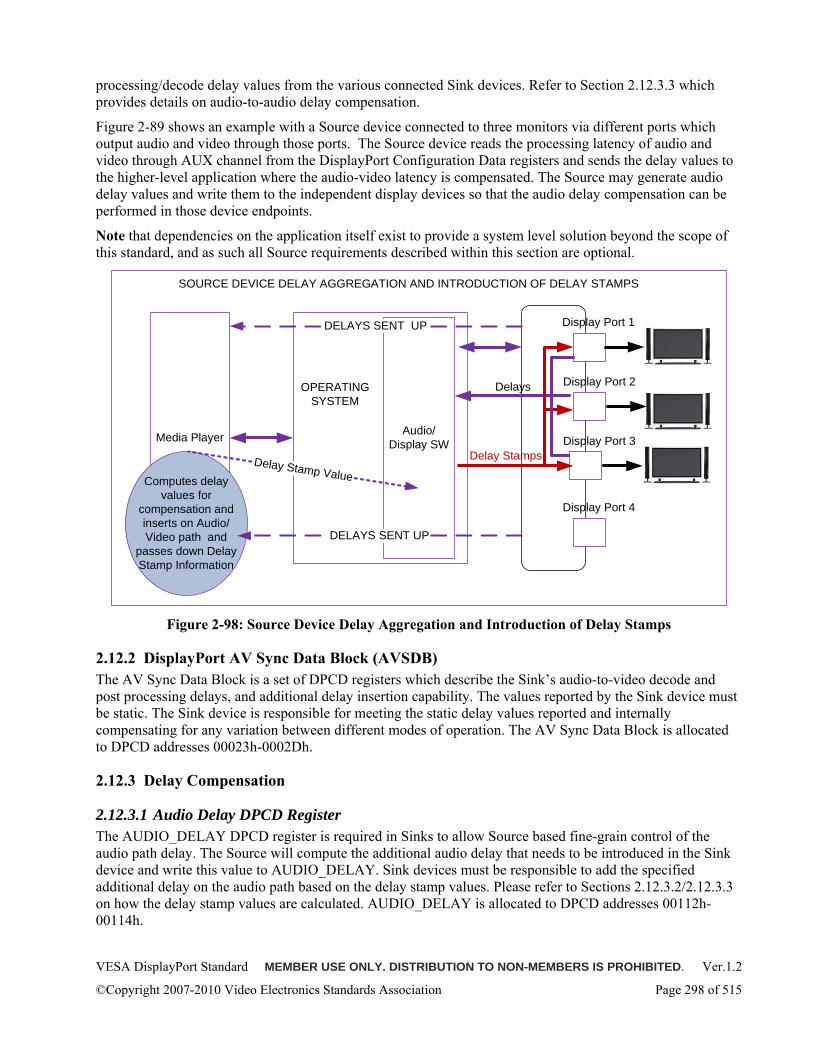
VESA DisplayPort Standard MEMBER USE ONLY. DISTRIBUTION TO NON-MEMBERS IS PROHIBITED. Ver.1.2
©Copyright 2007-2010 Video Electronics Standards Association Page 298 of 515
processing/decode delay values from the various connected Sink devices. Refer to Section 2.12.3.3 which provides details on audio-to-audio delay compensation.
Figure 2-89 shows an example with a Source device connected to three monitors via different ports which output audio and video through those ports. The Source device reads the processing latency of audio and video through AUX channel from the DisplayPort Configuration Data registers and sends the delay values to the higher-level application where the audio-video latency is compensated. The Source may generate audio delay values and write them to the independent display devices so that the audio delay compensation can be performed in those device endpoints.
Note that dependencies on the application itself exist to provide a system level solution beyond the scope of this standard, and as such all Source requirements described within this section are optional.
Media Player
Display Port 1
Display Port 2
Display Port 4
SOURCE DEVICE DELAY AGGREGATION AND INTRODUCTION OF DELAY STAMPS
Computes delay values for
compensation and inserts on Audio/Video path and
passes down Delay Stamp Information
Display Port 3
DelaysOPERATING SYSTEM
Audio/Display SW
DELAYS SENT UP
Delay Stamp Value
DELAYS SENT UP
Delay Stamps
Figure 2-98: Source Device Delay Aggregation and Introduction of Delay Stamps
2.12.2 DisplayPort AV Sync Data Block (AVSDB) The AV Sync Data Block is a set of DPCD registers which describe the Sink’s audio-to-video decode and post processing delays, and additional delay insertion capability. The values reported by the Sink device must be static. The Sink device is responsible for meeting the static delay values reported and internally compensating for any variation between different modes of operation. The AV Sync Data Block is allocated to DPCD addresses 00023h-0002Dh.
2.12.3 Delay Compensation
2.12.3.1 Audio Delay DPCD Register The AUDIO_DELAY DPCD register is required in Sinks to allow Source based fine-grain control of the audio path delay. The Source will compute the additional audio delay that needs to be introduced in the Sink device and write this value to AUDIO_DELAY. Sink devices must be responsible to add the specified additional delay on the audio path based on the delay stamp values. Please refer to Sections 2.12.3.2/2.12.3.3 on how the delay stamp values are calculated. AUDIO_DELAY is allocated to DPCD addresses 00112h-00114h.
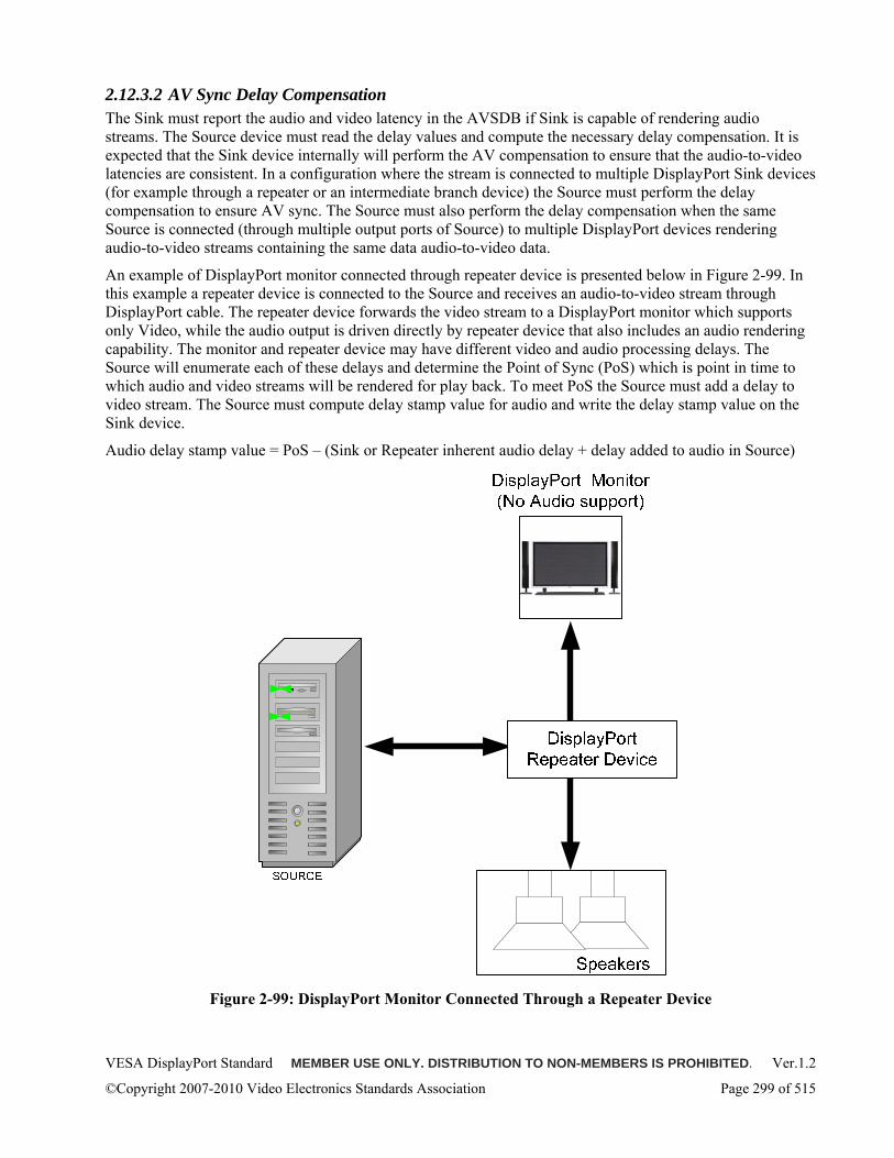
VESA DisplayPort Standard MEMBER USE ONLY. DISTRIBUTION TO NON-MEMBERS IS PROHIBITED. Ver.1.2
©Copyright 2007-2010 Video Electronics Standards Association Page 299 of 515
2.12.3.2 AV Sync Delay Compensation The Sink must report the audio and video latency in the AVSDB if Sink is capable of rendering audio streams. The Source device must read the delay values and compute the necessary delay compensation. It is expected that the Sink device internally will perform the AV compensation to ensure that the audio-to-video latencies are consistent. In a configuration where the stream is connected to multiple DisplayPort Sink devices (for example through a repeater or an intermediate branch device) the Source must perform the delay compensation to ensure AV sync. The Source must also perform the delay compensation when the same Source is connected (through multiple output ports of Source) to multiple DisplayPort devices rendering audio-to-video streams containing the same data audio-to-video data.
An example of DisplayPort monitor connected through repeater device is presented below in Figure 2-99. In this example a repeater device is connected to the Source and receives an audio-to-video stream through DisplayPort cable. The repeater device forwards the video stream to a DisplayPort monitor which supports only Video, while the audio output is driven directly by repeater device that also includes an audio rendering capability. The monitor and repeater device may have different video and audio processing delays. The Source will enumerate each of these delays and determine the Point of Sync (PoS) which is point in time to which audio and video streams will be rendered for play back. To meet PoS the Source must add a delay to video stream. The Source must compute delay stamp value for audio and write the delay stamp value on the Sink device.
Audio delay stamp value = PoS – (Sink or Repeater inherent audio delay + delay added to audio in Source)
Figure 2-99: DisplayPort Monitor Connected Through a Repeater Device
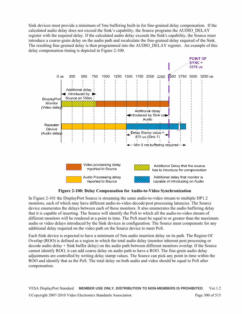
VESA DisplayPort Standard MEMBER USE ONLY. DISTRIBUTION TO NON-MEMBERS IS PROHIBITED. Ver.1.2
©Copyright 2007-2010 Video Electronics Standards Association Page 300 of 515
Sink devices must provide a minimum of 5ms buffering built-in for fine-grained delay compensation. If the calculated audio delay does not exceed the Sink’s capability, the Source programs the AUDIO_DELAY register with the required delay. If the calculated audio delay exceeds the Sink's capability, the Source must introduce a coarse-grain delay on the audio path and recalculate the fine-grained delay required of the Sink. The resulting fine-grained delay is then programmed into the AUDIO_DELAY register. An example of this delay compensation timing is depicted in Figure 2-100.
Figure 2-100: Delay Compensation for Audio-to-Video Synchronization
In Figure 2-101 the DisplayPort Source is streaming the same audio-to-video stream to multiple DP1.2 monitors, each of which may have different audio-to-video decode/post processing latencies. The Source device enumerates the delays between each of these monitors. It also enumerates the audio buffering delay that it is capable of inserting. The Source will identify the PoS to which all the audio-to-video stream of different monitors will be rendered at a point in time. The PoS must be equal to or greater than the maximum audio or video delays introduced by the Sink devices in configuration. The Source must compensate for any additional delay required on the video path on the Source device to meet PoS.
Each Sink device is expected to have a minimum of 5ms audio insertion delay on its path. The Region Of Overlap (ROO) is defined as a region in which the total audio delay (monitor inherent post processing or decode audio delay + Sink buffer delay) on the audio path between different monitors overlap. If the Source cannot identify ROO, it can add coarse delay on audio path to have a ROO. The fine-grain audio delay adjustments are controlled by writing delay stamp values. The Source can pick any point in time within the ROO and identify that as the PoS. The total delay on both audio and video should be equal to PoS after compensation.
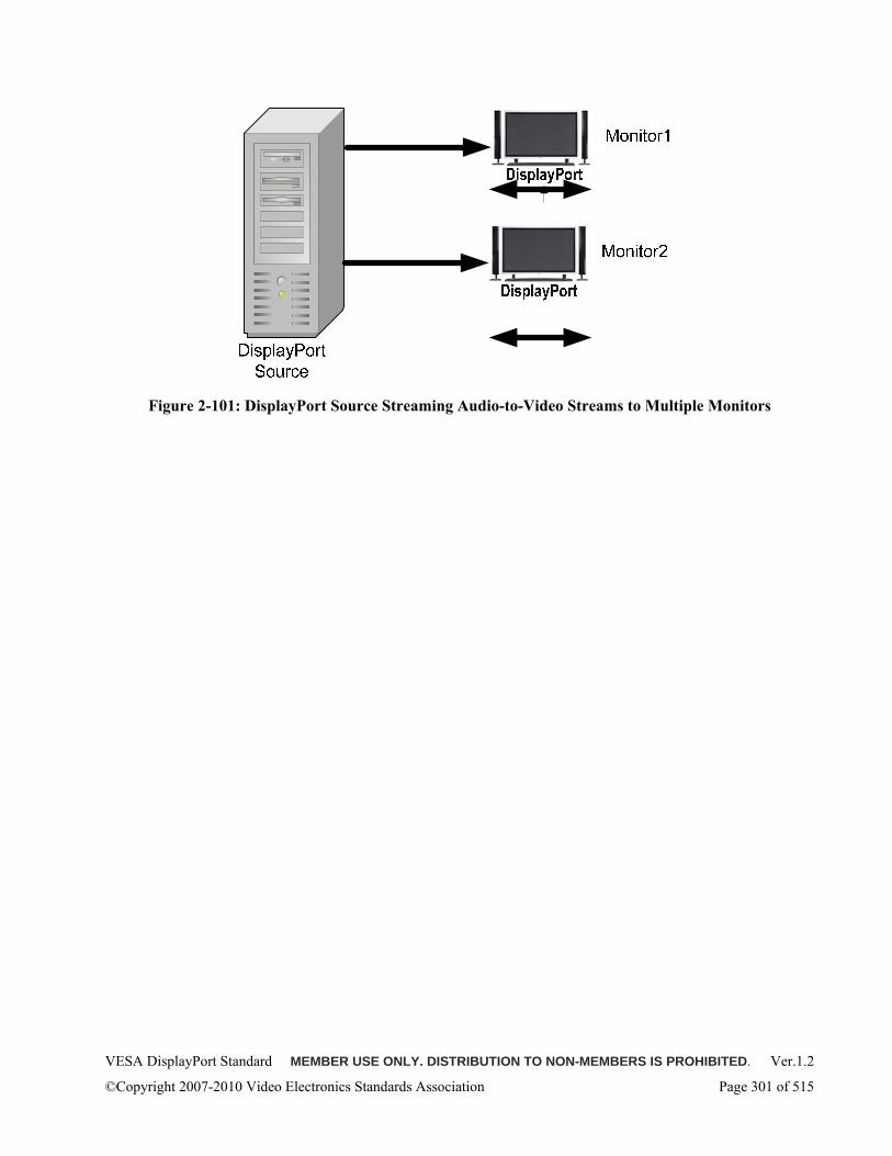
VESA DisplayPort Standard MEMBER USE ONLY. DISTRIBUTION TO NON-MEMBERS IS PROHIBITED. Ver.1.2
©Copyright 2007-2010 Video Electronics Standards Association Page 301 of 515
Figure 2-101: DisplayPort Source Streaming Audio-to-Video Streams to Multiple Monitors
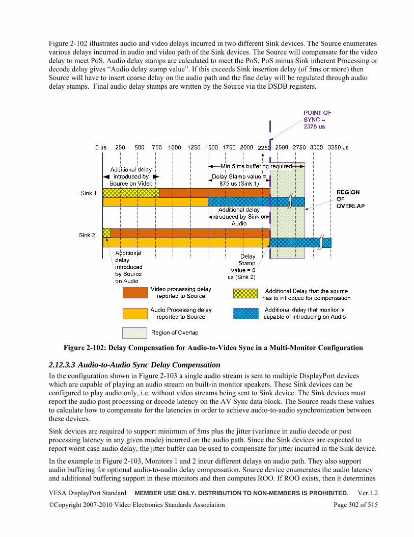
VESA DisplayPort Standard MEMBER USE ONLY. DISTRIBUTION TO NON-MEMBERS IS PROHIBITED. Ver.1.2
©Copyright 2007-2010 Video Electronics Standards Association Page 302 of 515
Figure 2-102 illustrates audio and video delays incurred in two different Sink devices. The Source enumerates various delays incurred in audio and video path of the Sink devices. The Source will compensate for the video delay to meet PoS. Audio delay stamps are calculated to meet the PoS, PoS minus Sink inherent Processing or decode delay gives “Audio delay stamp value”. If this exceeds Sink insertion delay (of 5ms or more) then Source will have to insert coarse delay on the audio path and the fine delay will be regulated through audio delay stamps. Final audio delay stamps are written by the Source via the DSDB registers.
Figure 2-102: Delay Compensation for Audio-to-Video Sync in a Multi-Monitor Configuration
2.12.3.3 Audio-to-Audio Sync Delay Compensation In the configuration shown in Figure 2-103 a single audio stream is sent to multiple DisplayPort devices which are capable of playing an audio stream on built-in monitor speakers. These Sink devices can be configured to play audio only, i.e. without video streams being sent to Sink device. The Sink devices must report the audio post processing or decode latency on the AV Sync data block. The Source reads these values to calculate how to compensate for the latencies in order to achieve audio-to-audio synchronization between these devices.
Sink devices are required to support minimum of 5ms plus the jitter (variance in audio decode or post processing latency in any given mode) incurred on the audio path. Since the Sink devices are expected to report worst case audio delay, the jitter buffer can be used to compensate for jitter incurred in the Sink device.
In the example in Figure 2-103, Monitors 1 and 2 incur different delays on audio path. They also support audio buffering for optional audio-to-audio delay compensation. Source device enumerates the audio latency and additional buffering support in these monitors and then computes ROO. If ROO exists, then it determines
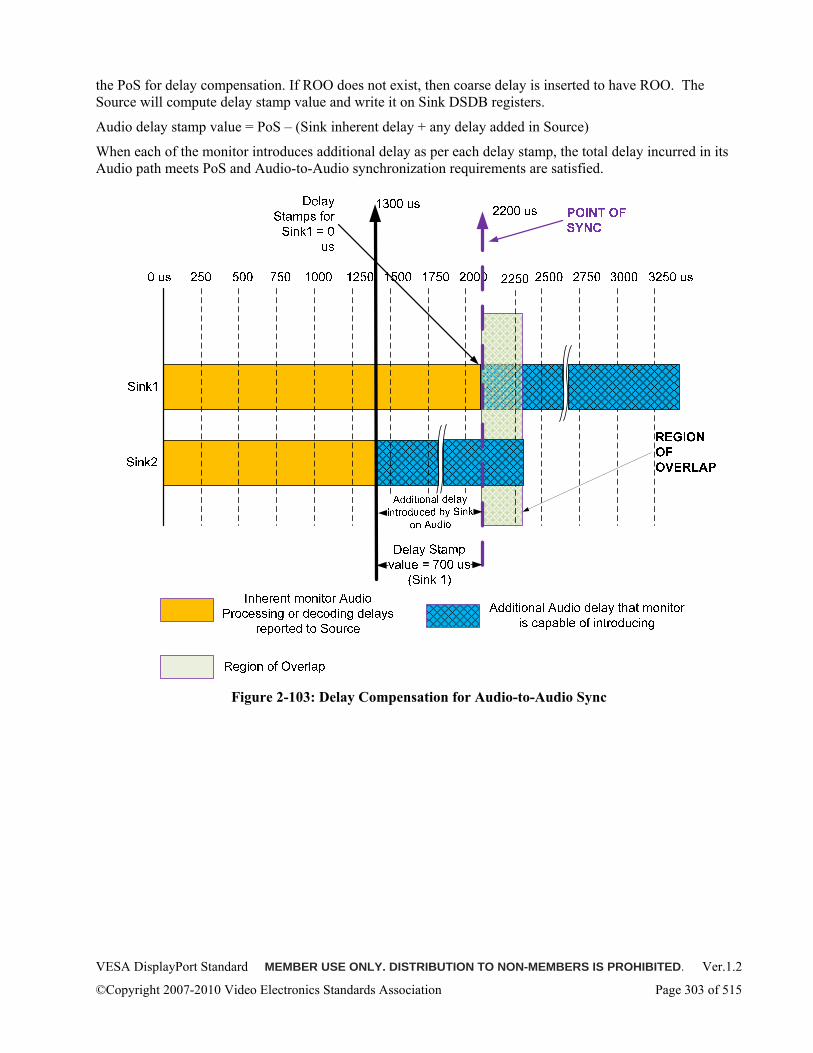
VESA DisplayPort Standard MEMBER USE ONLY. DISTRIBUTION TO NON-MEMBERS IS PROHIBITED. Ver.1.2
©Copyright 2007-2010 Video Electronics Standards Association Page 303 of 515
the PoS for delay compensation. If ROO does not exist, then coarse delay is inserted to have ROO. The Source will compute delay stamp value and write it on Sink DSDB registers.
Audio delay stamp value = PoS – (Sink inherent delay + any delay added in Source)
When each of the monitor introduces additional delay as per each delay stamp, the total delay incurred in its Audio path meets PoS and Audio-to-Audio synchronization requirements are satisfied.
Figure 2-103: Delay Compensation for Audio-to-Audio Sync
VESA DisplayPort Standard MEMBER USE ONLY. DISTRIBUTION TO NON-MEMBERS IS PROHIBITED. Ver.1.2
©Copyright 2007-2010 Video Electronics Standards Association Page 304 of 515
2.13 Global Time Code and Audio Inter-channel Sync This section describes the following two subjects:
o Introduction of the Global Time Code (GTC) of the DisplayPort Standard. The GTC is synchronized between DP devices across a DP link to a sub 100ns precision. This synchronization is repeated across the entire topology. One end of a link operates as GTC Master and the other end as GTC Slave. GTC Slave synchronizes its GTC value to that of GTC Master. Each GTC-capable device, whether an upstream device or a downstream device must be able to operate as either GTC Master or GTC Slave, though the upstream device is GTC Master by default.
o Application of GTC for realizing an audio inter-channel synchronization with sub 100ns precision when audio channels are rendered on multiple audio stream Sink devices connected via DP links.
2.13.1 Global Time Code The GTC is a 32-bit value, in units of 1ns (the lsb corresponds to 1ns). The GTC value of FFFFFFFFh corresponds to just less than 4.3 seconds. A protocol is defined using Native AUX transaction for DP devices across a DP link to align GTCs to sub 100ns precision.
Support of GTC is required for all DP devices supporting FAUX transaction. For those DP devices supporting Manchester transaction format only, support of GTC is required for DP Sink devices supporting audio and all DP Branch devices, and is recommended for DP Source devices supporting audio.
2.13.1.1 GTC Accumulator Requirement The GTC generator must be implemented as an accumulator driven by a GTC reference clock. How many counts the GTC value gets increased for each GTC reference clock depends on the GTC reference clock frequency and the precision of the accumulator. For example, if the GTC accumulator is 32 bits with the least significant bit corresponding to 1ns and if the GTC reference clock is 100MHz (that is, 10ns per clock cycle), the value is increased by 10 decimal counts per clock cycle.
GTC synchronization between a GTC Master and a GTC Slave consists of two phases; initial frequency adjust phase (lock acquisition phase) and the ensuing periodic frequency adjust phase (lock maintenance phase). During the lock acquisition phase (at the end of which the propagation delay over the DP link is adjusted), the GTC value is transferred from a GTC Master to a GTC Slave every 1ms, while the GTC value transfer takes place every 10ms during the lock maintenance phase.
The GTC reference clock on both ends must be 96MHz or higher during the initial frequency adjust phase, and 24MHz or higher during the periodic frequency adjust phase. No accumulation glitch is allowed when (or if) a reference clock is switched between an initial frequency adjust phase and a periodic frequency adjust phase. The reference clock must have a long-term accuracy of +/-100ppm from the nominal frequency. No spread-spectrum clocking is allowed for the GTC reference clock.
The difference between the GTC Master’s GTC value and the GTC Slave’s GTC value must settle to 25ns or smaller during the initial frequency adjust phase and stay 100ns or smaller during the periodic frequency adjust phase. The GTC Slave must be able to adjust the rate at which it increase the GTC value by adjusting the reference clock value, the increment value, or both the reference clock frequency and the increment value.
2.13.1.2 DPCD Fields for GTC The GTC synchronization involves the following register bits in the DPCD field
o RX_GTC_MSTR_REQ_STATUS_CHANGE (1 bit) o An IRQ Flag bit set by uPacket RX when it has changed the GTC_MSTR_REQ bit. Clearable
read-only for uPacket TX. o GTC_MSTR_REQ (1 bit)
o Set by uPacket RX when it wants to be GTC Master. Read-only for uPacket TX o GTC_RX_FREQ_LOCK_DONE (1 bit)
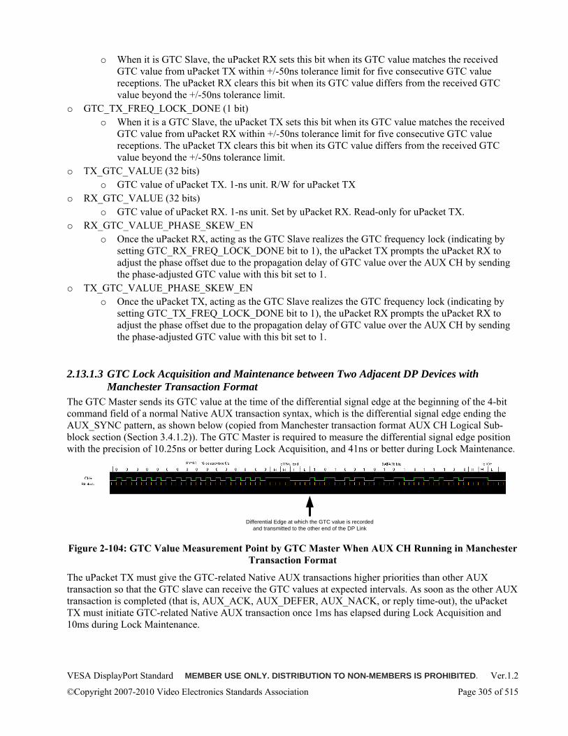
VESA DisplayPort Standard MEMBER USE ONLY. DISTRIBUTION TO NON-MEMBERS IS PROHIBITED. Ver.1.2
©Copyright 2007-2010 Video Electronics Standards Association Page 305 of 515
o When it is GTC Slave, the uPacket RX sets this bit when its GTC value matches the received GTC value from uPacket TX within +/-50ns tolerance limit for five consecutive GTC value receptions. The uPacket RX clears this bit when its GTC value differs from the received GTC value beyond the +/-50ns tolerance limit.
o GTC_TX_FREQ_LOCK_DONE (1 bit) o When it is a GTC Slave, the uPacket TX sets this bit when its GTC value matches the received
GTC value from uPacket RX within +/-50ns tolerance limit for five consecutive GTC value receptions. The uPacket TX clears this bit when its GTC value differs from the received GTC value beyond the +/-50ns tolerance limit.
o TX_GTC_VALUE (32 bits) o GTC value of uPacket TX. 1-ns unit. R/W for uPacket TX
o RX_GTC_VALUE (32 bits) o GTC value of uPacket RX. 1-ns unit. Set by uPacket RX. Read-only for uPacket TX.
o RX_GTC_VALUE_PHASE_SKEW_EN o Once the uPacket RX, acting as the GTC Slave realizes the GTC frequency lock (indicating by
setting GTC_RX_FREQ_LOCK_DONE bit to 1), the uPacket TX prompts the uPacket RX to adjust the phase offset due to the propagation delay of GTC value over the AUX CH by sending the phase-adjusted GTC value with this bit set to 1.
o TX_GTC_VALUE_PHASE_SKEW_EN o Once the uPacket TX, acting as the GTC Slave realizes the GTC frequency lock (indicating by
setting GTC_TX_FREQ_LOCK_DONE bit to 1), the uPacket RX prompts the uPacket RX to adjust the phase offset due to the propagation delay of GTC value over the AUX CH by sending the phase-adjusted GTC value with this bit set to 1.
2.13.1.3 GTC Lock Acquisition and Maintenance between Two Adjacent DP Devices with Manchester Transaction Format
The GTC Master sends its GTC value at the time of the differential signal edge at the beginning of the 4-bit command field of a normal Native AUX transaction syntax, which is the differential signal edge ending the AUX_SYNC pattern, as shown below (copied from Manchester transaction format AUX CH Logical Sub-block section (Section 3.4.1.2)). The GTC Master is required to measure the differential signal edge position with the precision of 10.25ns or better during Lock Acquisition, and 41ns or better during Lock Maintenance.
Differential Edge at which the GTC value is recorded and transmitted to the other end of the DP Link
Figure 2-104: GTC Value Measurement Point by GTC Master When AUX CH Running in Manchester Transaction Format
The uPacket TX must give the GTC-related Native AUX transactions higher priorities than other AUX transaction so that the GTC slave can receive the GTC values at expected intervals. As soon as the other AUX transaction is completed (that is, AUX_ACK, AUX_DEFER, AUX_NACK, or reply time-out), the uPacket TX must initiate GTC-related Native AUX transaction once 1ms has elapsed during Lock Acquisition and 10ms during Lock Maintenance.
VESA DisplayPort Standard MEMBER USE ONLY. DISTRIBUTION TO NON-MEMBERS IS PROHIBITED. Ver.1.2
©Copyright 2007-2010 Video Electronics Standards Association Page 306 of 515
The uPacket RX must not reply with AUX_DEFER. The uPacket RX must not reply with AUX_NACK or no reply unless the request transaction is corrupted. In case uPacket TX receives AUX_NACK or reply time-out, the uPacket TX must retry up to three times.
2.13.1.3.1 GTC Lock Acquisition/Maintenance Procedure When uPacket TX is the GTC Master The uPacket TX sends the GTC value at the time the AUXGTC value by writing the value to TX_GTC_VALUE (DPCD:00154h ~ 00157h) via Native AUX WR request transaction every 1ms. While the uPacket RX acting as GTC Slave is attempting to realize the frequency lock, it resets its GTC value to the received TX_GTC_VALUE and uses the delta between its GTC value and the received TX_GTC_VALUE to frequency adjust the GTC accumulator.
After 10 consecutive Native AUX WR transactions (for each of which it receives AUX_ACK reply), it reads the GTC_RX_FREQ_LOCK_DONE bit (DPCD 00059h bit 0) and RX_GTC_VALUE (DPCD 00054h ~ 00057h) by issuing a single Native AUX RD burst transaction to DPCD 00054h to 00059h.
If the GTC_RX_FREQ_LOCK_DONE bit does not get set, the uPacket TX may repeat the above procedure up to 10 times.
If the GTC_RX_FREQ_LOCK_DONE bit is set, the uPacket TX latches the RX_GTC_VALUE read in the same burst Native AUX RD transaction and compares it to its GTC value at the differential edge ending the AUX_SYNC pattern of reply transaction, and calculates the delta (which is its own GTC value at the differential edge minus the received uPacket RX GTC value). The phase offset is half of the delta.
The uPacket TX then writes the GTC value minus the phase offset to TX_GTC_VALUE with RX_GTC_VALUE_PHASE_SKEW _EN bit (DPCD 00158h bit 0) set to 1 via a single Native AUX burst write request transaction to DPCD 00154h ~ 00159h. Upon this Native AUX WR transaction, the uPacket RX resets its GTC value to the received TX_GTC_VALUE, but does not frequency adjust the GTC accumulator as RX_GTC_VALUE_PHASE_ SKEW_EN bit is set. After the completion of this read transaction, the uPacket TX clears the RX_GTC_VALUE_PHASE_SKEW_EN bit.
2.13.1.3.2 GTC Lock Acquisition/Maintenance Procedure When uPacket RX is the GTC Master The uPacket TX reads the GTC value of the uPacket RX by reading RX_GTC_VALUE (DPCD:00054h:00057h) and TX_GTC_VALUE_PHASE_ADJUST_EN bit (DPCD 00059h bit 1) via a single Native AUX burst read request transaction to DPCD 00054h ~ 00059h every 1ms. Upon the Native AUX RD reply transaction, the uPacket RX stores its GTC value at the differential edge ending the AUX SYNC pattern to RX_GTC_VALUE register. The uPacket TX reads the received RX_GTC_VALUE, resets its GTC value to the received RX_GTC_VALUE, and uses the delta between the GTC value and the received RX_GTC VALUE for frequency adjusting its GTC accumulator.
The uPacket TX continues the above Native AUX RD request transaction every 1ms until it realizes the GTC_TX_FREQ_LOCK_DONE. Once it realizes the GTC frequency lock, the uPacket TX sets the GTC_TX_FREQ_LOCK_DONE bit to 1 and writes its GTC value to TX_GTC_VALUE (DPCD:00154h:00157h) via Native AUX WR request transaction.
The uPacket RX compares its GTC value at the differential edge ending the AUX SYNC pattern of the request transaction to the received TX_GTC_VALUE from the uPacket TX, and calculates the delta (which is the receive TX_GTCP_VALUE from the uPacket TX minus its own GTC value). The phase offset is half of the delta.
Upon replying to the next Native AUX burst read request transaction to DPCD 00054h ~ 00059h, the uPacket RX sets the TX_GTC_VALUE_PHASE_SKEW_EN bit and stores the its GTC value minus the phase delta to RX_GTC_VALUE register. Once the phase adjusted GTC value is read by the uPacket TX, the uPacket RX clears the TX_GTC _VALUE_PHASE_SKEW_EN bit.
VESA DisplayPort Standard MEMBER USE ONLY. DISTRIBUTION TO NON-MEMBERS IS PROHIBITED. Ver.1.2
©Copyright 2007-2010 Video Electronics Standards Association Page 307 of 515
2.13.1.4 GTC Lock Acquisition/Maintenance Between Two Adjacent DP Devices with FAUX Transaction
The GTC Lock Acquisition/Maintenance procedure using FAUX transactions is the same as that using Manchester transaction format as described in Section 2.13.1.3. GTC Master sends the GTC value at the time the first serial bit of the 10-bit ANSI8B/10B-coded symbol of the first Command/Address field of Native AUX transaction is transmitted by the driver of the FAUX transmitter. GTC Slave compares the received GTC value to that of its own at the time its FAUX receiver receives the serial bit.
2.13.1.5 Selection of Grand GTC Master When multiple GTC-capable DP devices are connected via multiple DP links in a given topology, one device must be selected as a GTC Grand Master. A device connected to the GTC Grand Master becomes a GTC Slave. This GTC Slave device when it conducts the GTC synchronization with another device becomes a GTC Master. As a result of the series of GTC synchronizations, all DP devices in the topology become synchronized to the GTC Grand Master.
By default, an upstream device is GTC Master of any DP link. In other words, all the downstream devices keep RX_GTC_MSTR_REQ bit. When there is only one DP Source device, therefore, that DP Source device becomes the Grand GTC Master.
2.13.1.5.1 Selection of Grand GTC Master When Multiple Source Devices Present When there are multiple Source devices in a topology that has one or multiple Concentrator Branch devices, the first DP Source device to start GTC Lock Acquisition becomes Grand GTC Master.
When one of the upstream ports of a Concentrator (Upstream Port1) has either achieved the GTC Lock or has started the GTC Lock Acquisition with its upstream device (Upstream Device1), and when another upstream device (Upstream Device2) connected to the other upstream port (Upstream Port2) starts GTC Lock Acquisition, the Concentrator port takes the following actions:
o Set RX_GTC_MSTR_REQ bit to 1 in RX_GTC_MSTR_REQ field. o Set RX_GTC_MSTR_REQ_STATUS_CHANGE bit in DEVICE_SERVICE_IRQ_VECTOR_ESI1 field
and generate IRQ_HPD. o Upon IRQ_HPD handling by Upstream Device2, initiate GTC Lock Acquisition as GTC Master o Subsequently, maintain GTC Lock as GTC Master.
If Upstream Device2 is another Branch device, that Branch device is to re-initiate GTC Lock Acquisition as GTC Master to other downstream and upstream links if those links have already either started or achieved GTC Lock Acquisition.
If a Concentrator receives Native AUX transactions for GTC Lock Acquisition from multiple upstream devices simultaneously, the Concentrator accepts one of the upstream devices as GTC Master. To the upstream device that was not selected, the Concentrator replies with AUX_NACK, and initiate GTC Lock Acquisition as GTC Master as described above. How a Concentrator selects one upstream device it accepts as GTC Grand Master is an implementation-specific decision and is outside the scope of this Standard.
2.13.2 Application of GTC for Audio Inter-channel Synchronization Having established a common global time reference across all nodes, the DisplayPort audio stream Source must determine the GTC presentation time for each audio frame.
An audio frame consists of 192 audio samples. The DisplayPort audio stream Source must insert the desired GTC presentation time for the audio frame into the “Channel” field (“C” in Figure 2-105) in a bit serial fashion in the last 32 samples of an audio frame (Samples 161 to 192), starting with the most significant bit of the GTC in the first audio sample. The 32-bit GTC value represents the starting time of the presentation of immediately upcoming 192-sample audio frame.
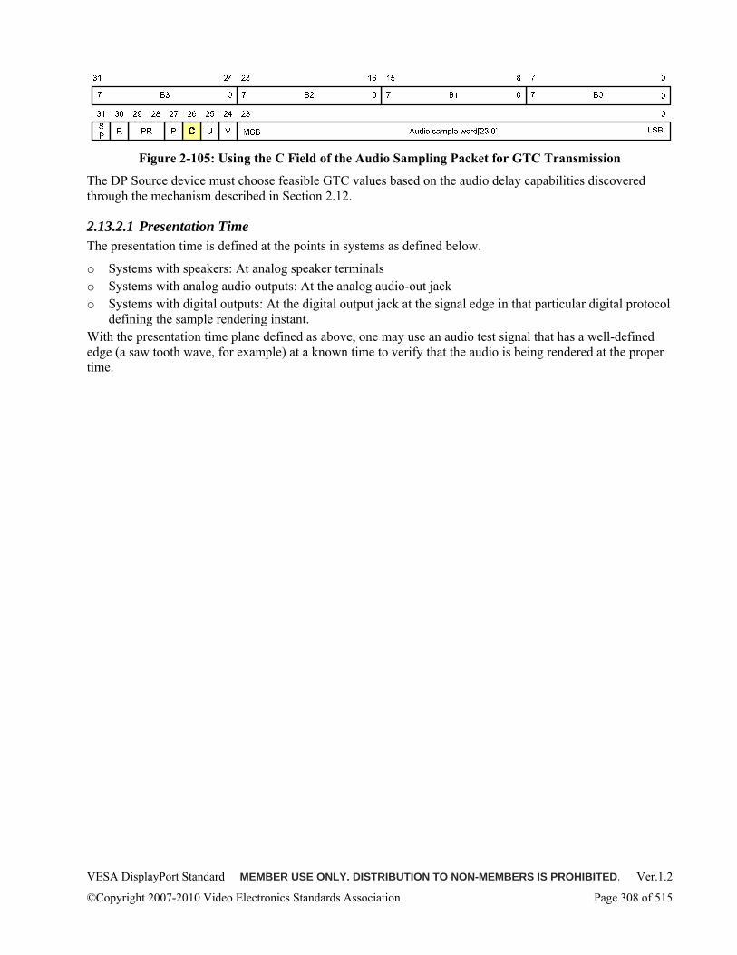
VESA DisplayPort Standard MEMBER USE ONLY. DISTRIBUTION TO NON-MEMBERS IS PROHIBITED. Ver.1.2
©Copyright 2007-2010 Video Electronics Standards Association Page 308 of 515
Figure 2-105: Using the C Field of the Audio Sampling Packet for GTC Transmission
The DP Source device must choose feasible GTC values based on the audio delay capabilities discovered through the mechanism described in Section 2.12.
2.13.2.1 Presentation Time The presentation time is defined at the points in systems as defined below.
o Systems with speakers: At analog speaker terminals o Systems with analog audio outputs: At the analog audio-out jack o Systems with digital outputs: At the digital output jack at the signal edge in that particular digital protocol
defining the sample rendering instant. With the presentation time plane defined as above, one may use an audio test signal that has a well-defined edge (a saw tooth wave, for example) at a known time to verify that the audio is being rendered at the proper time.
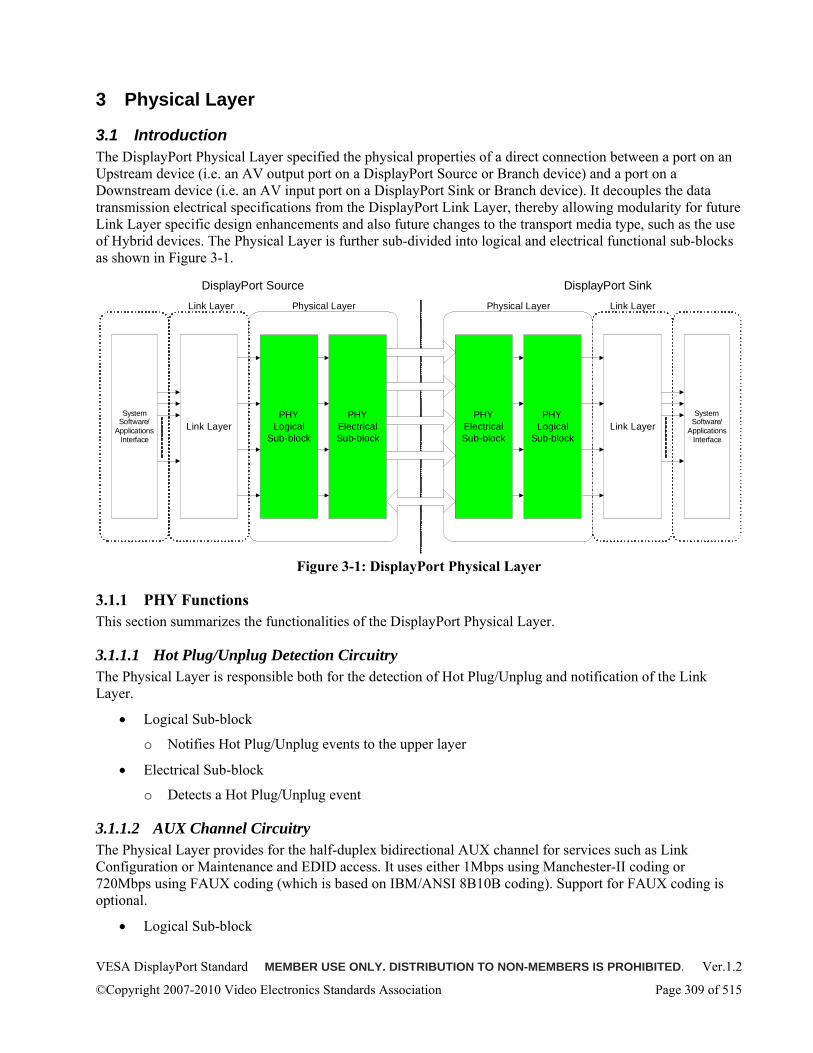
VESA DisplayPort Standard MEMBER USE ONLY. DISTRIBUTION TO NON-MEMBERS IS PROHIBITED. Ver.1.2
©Copyright 2007-2010 Video Electronics Standards Association Page 309 of 515
3 Physical Layer
3.1 Introduction The DisplayPort Physical Layer specified the physical properties of a direct connection between a port on an Upstream device (i.e. an AV output port on a DisplayPort Source or Branch device) and a port on a Downstream device (i.e. an AV input port on a DisplayPort Sink or Branch device). It decouples the data transmission electrical specifications from the DisplayPort Link Layer, thereby allowing modularity for future Link Layer specific design enhancements and also future changes to the transport media type, such as the use of Hybrid devices. The Physical Layer is further sub-divided into logical and electrical functional sub-blocks as shown in Figure 3-1.
PHY Electrical Sub-block
PHY Logical
Sub-blockLink Layer
System Software/
Applications Interface
Physical LayerLink Layer
PHY Logical
Sub-block
PHY Electrical Sub-block
Physical Layer
Link Layer System
Software/Applications
Interface
Link Layer
Greenland Source Greenland SinkDisplayPort Source DisplayPort Sink
Figure 3-1: DisplayPort Physical Layer
3.1.1 PHY Functions This section summarizes the functionalities of the DisplayPort Physical Layer.
3.1.1.1 Hot Plug/Unplug Detection Circuitry The Physical Layer is responsible both for the detection of Hot Plug/Unplug and notification of the Link Layer.
• Logical Sub-block
o Notifies Hot Plug/Unplug events to the upper layer
• Electrical Sub-block
o Detects a Hot Plug/Unplug event
3.1.1.2 AUX Channel Circuitry The Physical Layer provides for the half-duplex bidirectional AUX channel for services such as Link Configuration or Maintenance and EDID access. It uses either 1Mbps using Manchester-II coding or 720Mbps using FAUX coding (which is based on IBM/ANSI 8B10B coding). Support for FAUX coding is optional.
• Logical Sub-block
VESA DisplayPort Standard MEMBER USE ONLY. DISTRIBUTION TO NON-MEMBERS IS PROHIBITED. Ver.1.2
©Copyright 2007-2010 Video Electronics Standards Association Page 310 of 515
o Supports Manchester-II coding and, optionally, FAUX coding
o Generates and detects Start/Stop condition, and locks to the synchronization pattern for the appropriate encoding
o Encoding and decoding of data for the appropriate encoding
• Electrical Sub-block
o Consists of a single differential pair, both ends of the link equipped with driver and receiver for half-duplex bidirectional operation.
Driving end
o Drives a doubly terminated, AC-coupled differential pair in a manner compliant with the AUX channel electrical specification for the appropriate encoding (Manchester-II or FAUX)
Receiving end
o Receives the incoming differential signal and extracts the data
3.1.1.3 Main Link Circuitry The Physical Layer provides the unidirectional Main Link for the transport of isochronous streams and secondary-data packets.
• Logical Sub-block
o Scrambling and de-scrambling
o ANSI8B10B encoding/decoding
o Serialization and de-serialization
o Link Training and Link Status Monitor
Adjusts link rate, spreading, drive current level, pre-emphasis level and second cursor level as needed
o Link Quality Measurement for testability
• Electrical Sub-block
o Consists of up to four differential pairs
o Transmitter
Drives doubly terminated, AC-coupled differential pairs in a manner compliant with the Main Link Transmitter electrical specification
o Receiver
Receives the incoming differential signals and extract the data with its link CDR (clock and data recovery) circuits
3.1.2 Link Layer-PHY Interface Signals This section summarizes the interface signals between Link Layer and Physical Layer
3.1.2.1 Hot Plug/Unplug Detection Hot Plug/Unplug Detection circuitry provides for the Hot Plug/Unplug Status signal to Link Layer.
The de-bouncing timer must belong to Link Layer and not the Physical Layer.
VESA DisplayPort Standard MEMBER USE ONLY. DISTRIBUTION TO NON-MEMBERS IS PROHIBITED. Ver.1.2
©Copyright 2007-2010 Video Electronics Standards Association Page 311 of 515
3.1.2.2 AUX Channel The interface signal for the AUX channel between the Link and Physical Layers must consist of an 8-bit data signal plus 1-bit control signal. The control signal is used to indicate Start or Stop of the AUX CH transaction. The use of the 1-bit control signal to indicate Start/Stop conditions is implementation-specific and is not covered in this Standard.
3.1.2.3 Main Link The interface signal for the Main Link between the Link and Physical Layers consists of an 8-bit data signal per Main Link lane plus a 1-bit control signal. The control signal is used for special symbols such as BS (Blank Start) and BE (Blank End) for framing an isochronous data stream. The use of the 1-bit control signal is implementation-specific and is not covered in this Standard.
3.1.3 PHY-Media Interface Signals This section summarizes the interface signals between the Physical Layer and the Link Media consisting of PCB, connector, and cable. (Connector and cable may be absent for certain link configurations such as a chip-to-chip connection.)
3.1.3.1 DP_PWR / DP_PWR_RETURN A DisplayPort Source, Sink or locally powered Branch Device must provide power on the DP_PWR pin of the box-to-box DisplayPort connector. The power must be used only by a device that is directly connected to a Source, Sink or locally power Branch Device. In other words DP_PWR consumer devices must not be cascaded.
3.1.3.2 Hot Plug/Unplug Detection One signal (HPD) is used by a device (an Upstream device) to detect that a Downstream port on the device has been connected to another device (the Downstream device). Implementation of HPD is optional for an embedded link configuration. At least a “trickle power” must be present both in the Upstream and Downstream devices for a Hot Plug event to be detected.
Downstream devices must be ready for an AUX CH transaction whenever they assert (drive high) the HPD signal. Even in power saving mode(s) (see Section 5.2.5), a Downstream device that keeps its HPD signal asserted must be able to detect the presence of an AUX CH differential signal input. The Downstream device must exit the power saving mode within 1ms of the differential signal being detected.
3.1.3.3 AUX Channel The AUX Channel consists of one differential pair (AUX-CH+ and AUX-CH-).
At least “trickle power” must be present both in Upstream device and Downstream device for the AUX Channel to be functional.
A Downstream device that supports Upstream device detection, an optional feature, must monitor the DC voltage of the AUX CH lines between the AC coupling capacitors and its Upstream connector.
3.1.3.4 Main Link The Main Link consists of up to four differential pairs (Main Link Lane 0+, Main Link 0-, Main Link Lane 1+, Main-Link Lane 1- …).
Both the Upstream device and the Downstream device must be fully powered for the Main Link to be functional.
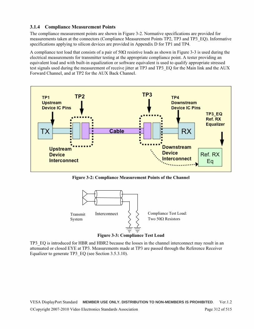
VESA DisplayPort Standard MEMBER USE ONLY. DISTRIBUTION TO NON-MEMBERS IS PROHIBITED. Ver.1.2
©Copyright 2007-2010 Video Electronics Standards Association Page 312 of 515
3.1.4 Compliance Measurement Points The compliance measurement points are shown in Figure 3-2. Normative specifications are provided for measurements taken at the connectors (Compliance Measurement Points TP2, TP3 and TP3_EQ). Informative specifications applying to silicon devices are provided in Appendix D for TP1 and TP4.
A compliance test load that consists of a pair of 50Ω resistive loads as shown in Figure 3-3 is used during the electrical measurements for transmitter testing at the appropriate compliance point. A tester providing an equivalent load and with built-in equalization or software equivalent is used to qualify appropriate stressed test signals used during the measurement of receive jitter at TP3 and TP3_EQ for the Main link and the AUX Forward Channel, and at TP2 for the AUX Back Channel.
Figure 3-2: Compliance Measurement Points of the Channel
Figure 3-3: Compliance Test Load
TP3_EQ is introduced for HBR and HBR2 because the losses in the channel interconnect may result in an attenuated or closed EYE at TP3. Measurements made at TP3 are passed through the Reference Receiver Equalizer to generate TP3_EQ (see Section 3.5.3.10).
Transmit System
Compliance Test Load: Two 50Ω Resistors
Interconnect
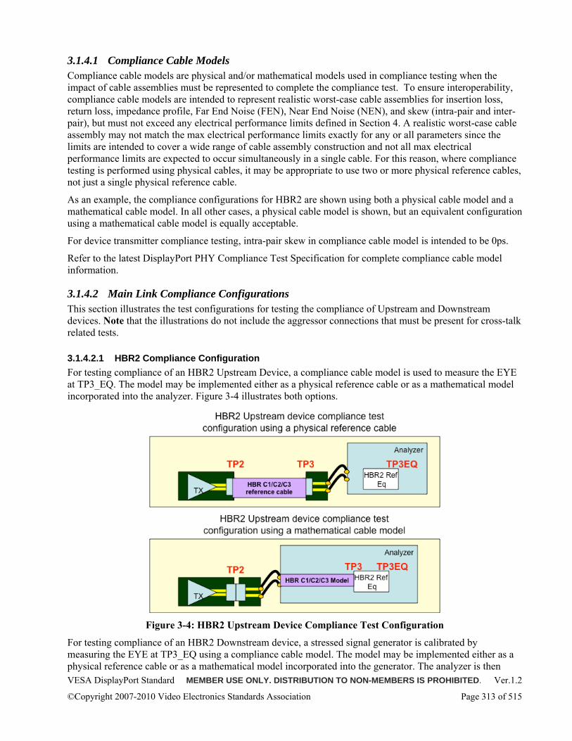
VESA DisplayPort Standard MEMBER USE ONLY. DISTRIBUTION TO NON-MEMBERS IS PROHIBITED. Ver.1.2
©Copyright 2007-2010 Video Electronics Standards Association Page 313 of 515
3.1.4.1 Compliance Cable Models Compliance cable models are physical and/or mathematical models used in compliance testing when the impact of cable assemblies must be represented to complete the compliance test. To ensure interoperability, compliance cable models are intended to represent realistic worst-case cable assemblies for insertion loss, return loss, impedance profile, Far End Noise (FEN), Near End Noise (NEN), and skew (intra-pair and inter-pair), but must not exceed any electrical performance limits defined in Section 4. A realistic worst-case cable assembly may not match the max electrical performance limits exactly for any or all parameters since the limits are intended to cover a wide range of cable assembly construction and not all max electrical performance limits are expected to occur simultaneously in a single cable. For this reason, where compliance testing is performed using physical cables, it may be appropriate to use two or more physical reference cables, not just a single physical reference cable.
As an example, the compliance configurations for HBR2 are shown using both a physical cable model and a mathematical cable model. In all other cases, a physical cable model is shown, but an equivalent configuration using a mathematical cable model is equally acceptable.
For device transmitter compliance testing, intra-pair skew in compliance cable model is intended to be 0ps.
Refer to the latest DisplayPort PHY Compliance Test Specification for complete compliance cable model information.
3.1.4.2 Main Link Compliance Configurations This section illustrates the test configurations for testing the compliance of Upstream and Downstream devices. Note that the illustrations do not include the aggressor connections that must be present for cross-talk related tests.
3.1.4.2.1 HBR2 Compliance Configuration For testing compliance of an HBR2 Upstream Device, a compliance cable model is used to measure the EYE at TP3_EQ. The model may be implemented either as a physical reference cable or as a mathematical model incorporated into the analyzer. Figure 3-4 illustrates both options.
Figure 3-4: HBR2 Upstream Device Compliance Test Configuration
For testing compliance of an HBR2 Downstream device, a stressed signal generator is calibrated by measuring the EYE at TP3_EQ using a compliance cable model. The model may be implemented either as a physical reference cable or as a mathematical model incorporated into the generator. The analyzer is then
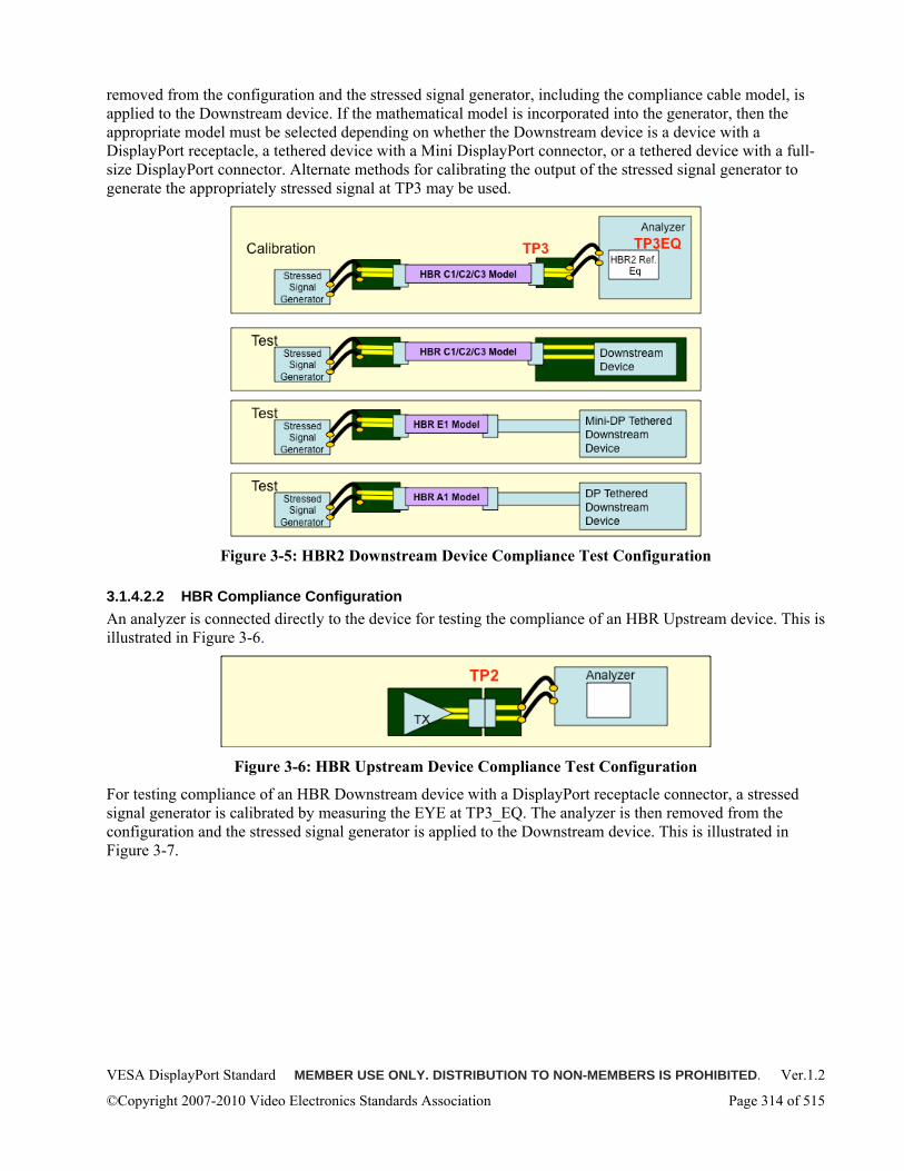
VESA DisplayPort Standard MEMBER USE ONLY. DISTRIBUTION TO NON-MEMBERS IS PROHIBITED. Ver.1.2
©Copyright 2007-2010 Video Electronics Standards Association Page 314 of 515
removed from the configuration and the stressed signal generator, including the compliance cable model, is applied to the Downstream device. If the mathematical model is incorporated into the generator, then the appropriate model must be selected depending on whether the Downstream device is a device with a DisplayPort receptacle, a tethered device with a Mini DisplayPort connector, or a tethered device with a full-size DisplayPort connector. Alternate methods for calibrating the output of the stressed signal generator to generate the appropriately stressed signal at TP3 may be used.
Figure 3-5: HBR2 Downstream Device Compliance Test Configuration
3.1.4.2.2 HBR Compliance Configuration An analyzer is connected directly to the device for testing the compliance of an HBR Upstream device. This is illustrated in Figure 3-6.
Figure 3-6: HBR Upstream Device Compliance Test Configuration
For testing compliance of an HBR Downstream device with a DisplayPort receptacle connector, a stressed signal generator is calibrated by measuring the EYE at TP3_EQ. The analyzer is then removed from the configuration and the stressed signal generator is applied to the Downstream device. This is illustrated in Figure 3-7.
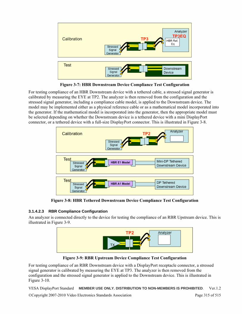
VESA DisplayPort Standard MEMBER USE ONLY. DISTRIBUTION TO NON-MEMBERS IS PROHIBITED. Ver.1.2
©Copyright 2007-2010 Video Electronics Standards Association Page 315 of 515
Figure 3-7: HBR Downstream Device Compliance Test Configuration
For testing compliance of an HBR Downstream device with a tethered cable, a stressed signal generator is calibrated by measuring the EYE at TP2. The analyzer is then removed from the configuration and the stressed signal generator, including a compliance cable model, is applied to the Downstream device. The model may be implemented either as a physical reference cable or as a mathematical model incorporated into the generator. If the mathematical model is incorporated into the generator, then the appropriate model must be selected depending on whether the Downstream device is a tethered device with a mini DisplayPort connector, or a tethered device with a full-size DisplayPort connector. This is illustrated in Figure 3-8.
Figure 3-8: HBR Tethered Downstream Device Compliance Test Configuration
3.1.4.2.3 RBR Compliance Configuration An analyzer is connected directly to the device for testing the compliance of an RBR Upstream device. This is illustrated in Figure 3-9.
Figure 3-9: RBR Upstream Device Compliance Test Configuration
For testing compliance of an RBR Downstream device with a DisplayPort receptacle connector, a stressed signal generator is calibrated by measuring the EYE at TP3. The analyzer is then removed from the configuration and the stressed signal generator is applied to the Downstream device. This is illustrated in Figure 3-10.
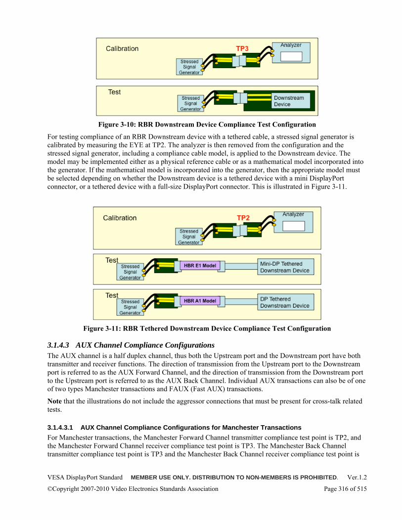
VESA DisplayPort Standard MEMBER USE ONLY. DISTRIBUTION TO NON-MEMBERS IS PROHIBITED. Ver.1.2
©Copyright 2007-2010 Video Electronics Standards Association Page 316 of 515
Figure 3-10: RBR Downstream Device Compliance Test Configuration
For testing compliance of an RBR Downstream device with a tethered cable, a stressed signal generator is calibrated by measuring the EYE at TP2. The analyzer is then removed from the configuration and the stressed signal generator, including a compliance cable model, is applied to the Downstream device. The model may be implemented either as a physical reference cable or as a mathematical model incorporated into the generator. If the mathematical model is incorporated into the generator, then the appropriate model must be selected depending on whether the Downstream device is a tethered device with a mini DisplayPort connector, or a tethered device with a full-size DisplayPort connector. This is illustrated in Figure 3-11.
Figure 3-11: RBR Tethered Downstream Device Compliance Test Configuration
3.1.4.3 AUX Channel Compliance Configurations The AUX channel is a half duplex channel, thus both the Upstream port and the Downstream port have both transmitter and receiver functions. The direction of transmission from the Upstream port to the Downstream port is referred to as the AUX Forward Channel, and the direction of transmission from the Downstream port to the Upstream port is referred to as the AUX Back Channel. Individual AUX transactions can also be of one of two types Manchester transactions and FAUX (Fast AUX) transactions.
Note that the illustrations do not include the aggressor connections that must be present for cross-talk related tests.
3.1.4.3.1 AUX Channel Compliance Configurations for Manchester Transactions For Manchester transactions, the Manchester Forward Channel transmitter compliance test point is TP2, and the Manchester Forward Channel receiver compliance test point is TP3. The Manchester Back Channel transmitter compliance test point is TP3 and the Manchester Back Channel receiver compliance test point is
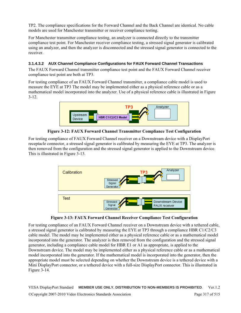
VESA DisplayPort Standard MEMBER USE ONLY. DISTRIBUTION TO NON-MEMBERS IS PROHIBITED. Ver.1.2
©Copyright 2007-2010 Video Electronics Standards Association Page 317 of 515
TP2. The compliance specifications for the Forward Channel and the Back Channel are identical. No cable models are used for Manchester transmitter or receiver compliance testing.
For Manchester transmitter compliance testing, an analyzer is connected directly to the transmitter compliance test point. For Manchester receiver compliance testing, a stressed signal generator is calibrated using an analyzer, and then the analyzer is disconnected and the stressed signal generator is connected to the receiver.
3.1.4.3.2 AUX Channel Compliance Configurations for FAUX Forward Channel Transactions The FAUX Forward Channel transmitter compliance test point and the FAUX Forward Channel receiver compliance test point are both at TP3.
For testing compliance of an FAUX Forward Channel transmitter, a compliance cable model is used to measure the EYE at TP3 The model may be implemented either as a physical reference cable or as a mathematical model incorporated into the analyzer. Use of a physical reference cable is illustrated in Figure 3-12.
Figure 3-12: FAUX Forward Channel Transmitter Compliance Test Configuration
For testing compliance of FAUX Forward Channel receiver on a Downstream device with a DisplayPort receptacle connector, a stressed signal generator is calibrated by measuring the EYE at TP3. The analyzer is then removed from the configuration and the stressed signal generator is applied to the Downstream device. This is illustrated in Figure 3-13.
Figure 3-13: FAUX Forward Channel Receiver Compliance Test Configuration
For testing compliance of an FAUX Forward Channel receiver on a Downstream device with a tethered cable, a stressed signal generator is calibrated by measuring the EYE at TP3 through a compliance HBR C1/C2/C3 cable model. The model may be implemented either as a physical reference cable or as a mathematical model incorporated into the generator. The analyzer is then removed from the configuration and the stressed signal generator, including a compliance cable model for HBR E1 or A1 as appropriate, is applied to the Downstream device. The model may be implemented either as a physical reference cable or as a mathematical model incorporated into the generator. If the mathematical model is incorporated into the generator, then the appropriate model must be selected depending on whether the Downstream device is a tethered device with a Mini DisplayPort connector, or a tethered device with a full-size DisplayPort connector. This is illustrated in Figure 3-14.
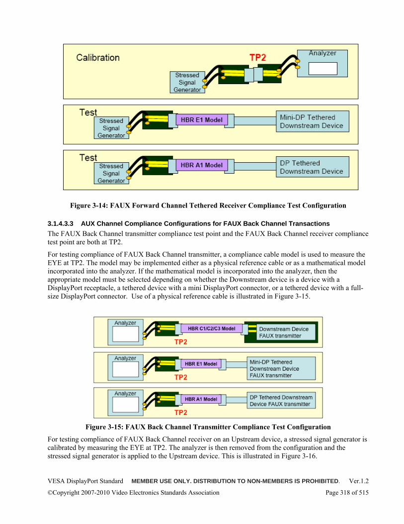
VESA DisplayPort Standard MEMBER USE ONLY. DISTRIBUTION TO NON-MEMBERS IS PROHIBITED. Ver.1.2
©Copyright 2007-2010 Video Electronics Standards Association Page 318 of 515
Figure 3-14: FAUX Forward Channel Tethered Receiver Compliance Test Configuration
3.1.4.3.3 AUX Channel Compliance Configurations for FAUX Back Channel Transactions The FAUX Back Channel transmitter compliance test point and the FAUX Back Channel receiver compliance test point are both at TP2.
For testing compliance of FAUX Back Channel transmitter, a compliance cable model is used to measure the EYE at TP2. The model may be implemented either as a physical reference cable or as a mathematical model incorporated into the analyzer. If the mathematical model is incorporated into the analyzer, then the appropriate model must be selected depending on whether the Downstream device is a device with a DisplayPort receptacle, a tethered device with a mini DisplayPort connector, or a tethered device with a full-size DisplayPort connector. Use of a physical reference cable is illustrated in Figure 3-15.
Figure 3-15: FAUX Back Channel Transmitter Compliance Test Configuration
For testing compliance of FAUX Back Channel receiver on an Upstream device, a stressed signal generator is calibrated by measuring the EYE at TP2. The analyzer is then removed from the configuration and the stressed signal generator is applied to the Upstream device. This is illustrated in Figure 3-16.
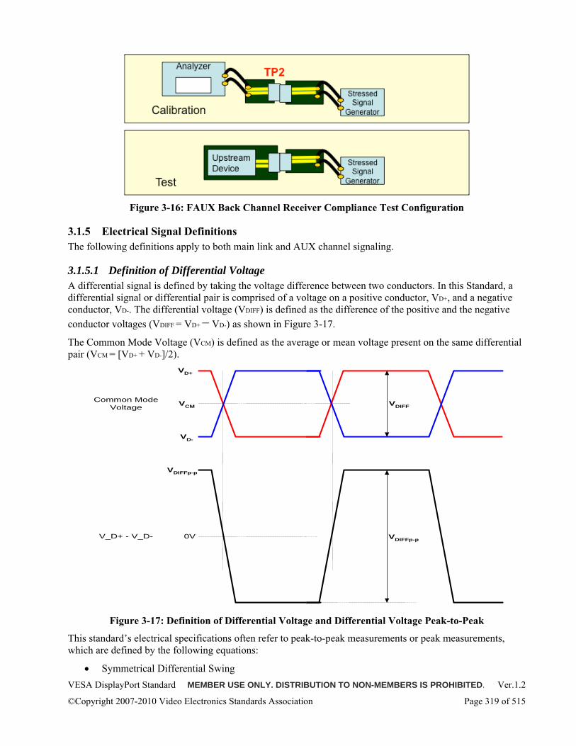
VESA DisplayPort Standard MEMBER USE ONLY. DISTRIBUTION TO NON-MEMBERS IS PROHIBITED. Ver.1.2
©Copyright 2007-2010 Video Electronics Standards Association Page 319 of 515
Figure 3-16: FAUX Back Channel Receiver Compliance Test Configuration
3.1.5 Electrical Signal Definitions The following definitions apply to both main link and AUX channel signaling.
3.1.5.1 Definition of Differential Voltage A differential signal is defined by taking the voltage difference between two conductors. In this Standard, a differential signal or differential pair is comprised of a voltage on a positive conductor, VD+, and a negative conductor, VD-. The differential voltage (VDIFF) is defined as the difference of the positive and the negative conductor voltages (VDIFF = VD+ − VD-) as shown in Figure 3-17.
The Common Mode Voltage (VCM) is defined as the average or mean voltage present on the same differential pair (VCM = [VD+ + VD-]/2).
VD+
Common ModeVoltage
V_D+ - V_D- 0V
VCM VDIFF
VD-
VDIFFp-p
VDIFFp-p
Figure 3-17: Definition of Differential Voltage and Differential Voltage Peak-to-Peak
This standard’s electrical specifications often refer to peak-to-peak measurements or peak measurements, which are defined by the following equations:
• Symmetrical Differential Swing
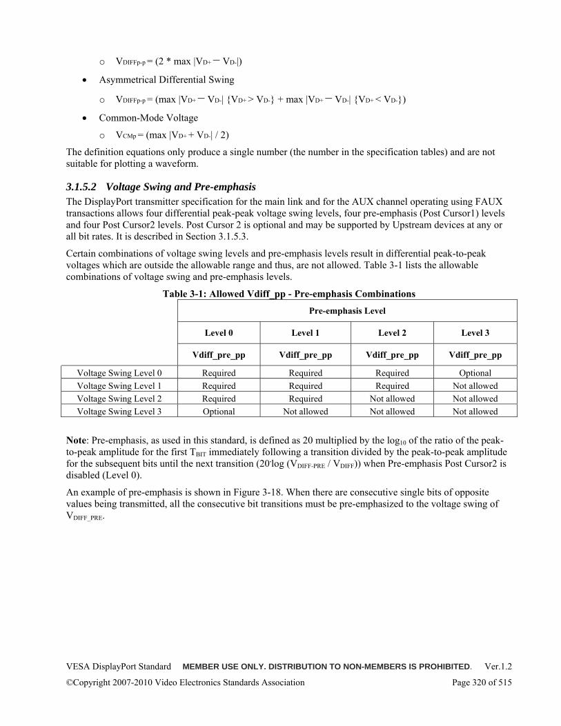
VESA DisplayPort Standard MEMBER USE ONLY. DISTRIBUTION TO NON-MEMBERS IS PROHIBITED. Ver.1.2
©Copyright 2007-2010 Video Electronics Standards Association Page 320 of 515
o VDIFFp-p = (2 * max |VD+ − VD-|)
• Asymmetrical Differential Swing
o VDIFFp-p = (max |VD+ − VD-| VD+ > VD- + max |VD+ − VD-| VD+ < VD-)
• Common-Mode Voltage
o VCMp = (max |VD+ + VD-| / 2)
The definition equations only produce a single number (the number in the specification tables) and are not suitable for plotting a waveform.
3.1.5.2 Voltage Swing and Pre-emphasis The DisplayPort transmitter specification for the main link and for the AUX channel operating using FAUX transactions allows four differential peak-peak voltage swing levels, four pre-emphasis (Post Cursor1) levels and four Post Cursor2 levels. Post Cursor 2 is optional and may be supported by Upstream devices at any or all bit rates. It is described in Section 3.1.5.3.
Certain combinations of voltage swing levels and pre-emphasis levels result in differential peak-to-peak voltages which are outside the allowable range and thus, are not allowed. Table 3-1 lists the allowable combinations of voltage swing and pre-emphasis levels.
Table 3-1: Allowed Vdiff_pp - Pre-emphasis Combinations
Pre-emphasis Level
Level 0 Level 1 Level 2 Level 3
Vdiff_pre_pp Vdiff_pre_pp Vdiff_pre_pp Vdiff_pre_pp
Voltage Swing Level 0 Required Required Required Optional Voltage Swing Level 1 Required Required Required Not allowed Voltage Swing Level 2 Required Required Not allowed Not allowed Voltage Swing Level 3 Optional Not allowed Not allowed Not allowed
Note: Pre-emphasis, as used in this standard, is defined as 20 multiplied by the log10 of the ratio of the peak-to-peak amplitude for the first TBIT immediately following a transition divided by the peak-to-peak amplitude for the subsequent bits until the next transition (20.log (VDIFF-PRE / VDIFF)) when Pre-emphasis Post Cursor2 is disabled (Level 0).
An example of pre-emphasis is shown in Figure 3-18. When there are consecutive single bits of opposite values being transmitted, all the consecutive bit transitions must be pre-emphasized to the voltage swing of VDIFF_PRE.
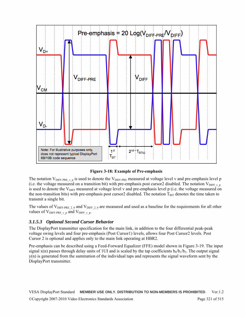
VESA DisplayPort Standard MEMBER USE ONLY. DISTRIBUTION TO NON-MEMBERS IS PROHIBITED. Ver.1.2
©Copyright 2007-2010 Video Electronics Standards Association Page 321 of 515
Figure 3-18: Example of Pre-emphasis
The notation VDIFF-PRE_v_p is used to denote the VDIFF-PRE measured at voltage level v and pre-emphasis level p (i.e. the voltage measured on a transition bit) with pre-emphasis post cursor2 disabled. The notation VDIFF_v_p is used to denote the VDIFF measured at voltage level v and pre-emphasis level p (i.e. the voltage measured on the non-transition bits) with pre-emphasis post cursor2 disabled. The notation TBIT denotes the time taken to transmit a single bit.
The values of VDIFF-PRE_2_0 and VDIFF_2_0 are measured and used as a baseline for the requirements for all other values of VDIFF-PRE_v_p and VDIFF_v_p.
3.1.5.3 Optional Second Cursor Behavior The DisplayPort transmitter specification for the main link, in addition to the four differential peak-peak voltage swing levels and four pre-emphasis (Post Cursor1) levels, allows four Post Cursor2 levels. Post Cursor 2 is optional and applies only to the main link operating at HBR2.
Pre-emphasis can be described using a Feed-Forward Equalizer (FFE) model shown in Figure 3-19. The input signal x(n) passes through delay units of 1UI and is scaled by the tap coefficients b0/b1/b2. The output signal y(n) is generated from the summation of the individual taps and represents the signal waveform sent by the DisplayPort transmitter.
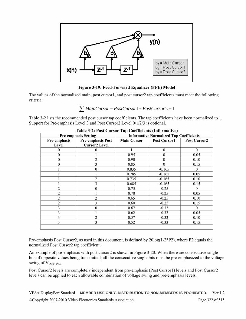
VESA DisplayPort Standard MEMBER USE ONLY. DISTRIBUTION TO NON-MEMBERS IS PROHIBITED. Ver.1.2
©Copyright 2007-2010 Video Electronics Standards Association Page 322 of 515
Figure 3-19: Feed-Forward Equalizer (FFE) Model
The values of the normalized main, post cursor1, and post cursor2 tap coefficients must meet the following criteria:
∑ =+− 121 PostCursorPostCursorMainCursor
Table 3-2 lists the recommended post cursor tap coefficients. The tap coefficients have been normalized to 1. Support for Pre-emphasis Level 3 and Post Cursor2 Level 0/1/2/3 is optional.
Table 3-2: Post Cursor Tap Coefficients (Informative) Pre-emphasis Setting Informative Normalized Tap Coefficients
Pre-emphasis Level
Pre-emphasis Post Cursor2 Level
Main Cursor Post Cursor1 Post Cursor2
0 0 1 0 0 0 1 0.95 0 0.05 0 2 0.90 0 0.10 0 3 0.85 0 0.15 1 0 0.835 -0.165 0 1 1 0.785 -0.165 0.05 1 2 0.735 -0.165 0.10 1 3 0.685 -0.165 0.15 2 0 0.75 -0.25 0 2 1 0.70 -0.25 0.05 2 2 0.65 -0.25 0.10 2 3 0.60 -0.25 0.15 3 0 0.67 -0.33 0 3 1 0.62 -0.33 0.05 3 2 0.57 -0.33 0.10 3 3 0.52 -0.33 0.15
Pre-emphasis Post Cursor2, as used in this document, is defined by 20log(1-2*P2), where P2 equals the normalized Post Cursor2 tap coefficient.
An example of pre-emphasis with post cursor2 is shown in Figure 3-20. When there are consecutive single bits of opposite values being transmitted, all the consecutive single bits must be pre-emphasized to the voltage swing of VDIFF_PRE.
Post Cursor2 levels are completely independent from pre-emphasis (Post Cursor1) levels and Post Cursor2 levels can be applied to each allowable combination of voltage swing and pre-emphasis levels.
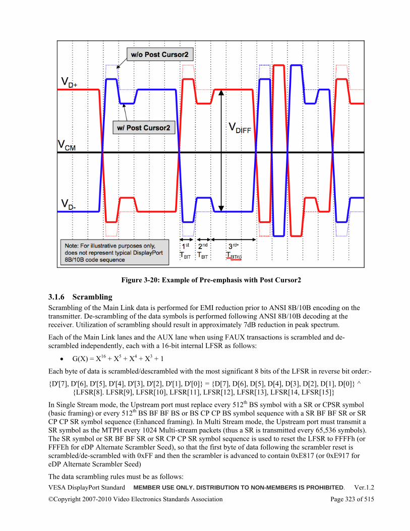
VESA DisplayPort Standard MEMBER USE ONLY. DISTRIBUTION TO NON-MEMBERS IS PROHIBITED. Ver.1.2
©Copyright 2007-2010 Video Electronics Standards Association Page 323 of 515
Figure 3-20: Example of Pre-emphasis with Post Cursor2
3.1.6 Scrambling Scrambling of the Main Link data is performed for EMI reduction prior to ANSI 8B/10B encoding on the transmitter. De-scrambling of the data symbols is performed following ANSI 8B/10B decoding at the receiver. Utilization of scrambling should result in approximately 7dB reduction in peak spectrum.
Each of the Main Link lanes and the AUX lane when using FAUX transactions is scrambled and de-scrambled independently, each with a 16-bit internal LFSR as follows:
• G(X) = X16 + X5 + X4 + X3 + 1
Each byte of data is scrambled/descrambled with the most significant 8 bits of the LFSR in reverse bit order:-
D'[7], D'[6], D'[5], D'[4], D'[3], D'[2], D'[1], D'[0] = D[7], D[6], D[5], D[4], D[3], D[2], D[1], D[0] ^ LFSR[8]. LFSR[9], LFSR[10], LFSR[11], LFSR[12], LFSR[13], LFSR[14, LFSR[15]
In Single Stream mode, the Upstream port must replace every 512th BS symbol with a SR or CPSR symbol (basic framing) or every 512th BS BF BF BS or BS CP CP BS symbol sequence with a SR BF BF SR or SR CP CP SR symbol sequence (Enhanced framing). In Multi Stream mode, the Upstream port must transmit a SR symbol as the MTPH every 1024 Multi-stream packets (thus a SR is transmitted every 65,536 symbols). The SR symbol or SR BF BF SR or SR CP CP SR symbol sequence is used to reset the LFSR to FFFFh (or FFFEh for eDP Alternate Scrambler Seed), so that the first byte of data following the scrambler reset is scrambled/de-scrambled with 0xFF and then the scrambler is advanced to contain 0xE817 (or 0xE917 for eDP Alternate Scrambler Seed)
The data scrambling rules must be as follows:
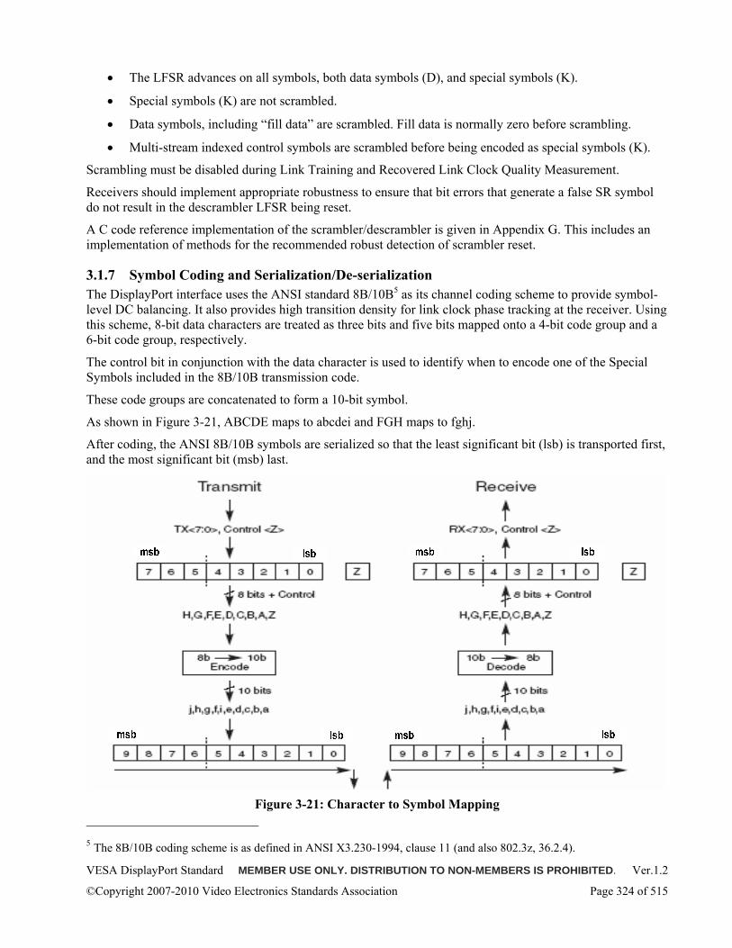
VESA DisplayPort Standard MEMBER USE ONLY. DISTRIBUTION TO NON-MEMBERS IS PROHIBITED. Ver.1.2
©Copyright 2007-2010 Video Electronics Standards Association Page 324 of 515
• The LFSR advances on all symbols, both data symbols (D), and special symbols (K).
• Special symbols (K) are not scrambled.
• Data symbols, including “fill data” are scrambled. Fill data is normally zero before scrambling.
• Multi-stream indexed control symbols are scrambled before being encoded as special symbols (K).
Scrambling must be disabled during Link Training and Recovered Link Clock Quality Measurement.
Receivers should implement appropriate robustness to ensure that bit errors that generate a false SR symbol do not result in the descrambler LFSR being reset.
A C code reference implementation of the scrambler/descrambler is given in Appendix G. This includes an implementation of methods for the recommended robust detection of scrambler reset.
3.1.7 Symbol Coding and Serialization/De-serialization The DisplayPort interface uses the ANSI standard 8B/10B5 as its channel coding scheme to provide symbol-level DC balancing. It also provides high transition density for link clock phase tracking at the receiver. Using this scheme, 8-bit data characters are treated as three bits and five bits mapped onto a 4-bit code group and a 6-bit code group, respectively.
The control bit in conjunction with the data character is used to identify when to encode one of the Special Symbols included in the 8B/10B transmission code.
These code groups are concatenated to form a 10-bit symbol.
As shown in Figure 3-21, ABCDE maps to abcdei and FGH maps to fghj.
After coding, the ANSI 8B/10B symbols are serialized so that the least significant bit (lsb) is transported first, and the most significant bit (msb) last.
Figure 3-21: Character to Symbol Mapping
5 The 8B/10B coding scheme is as defined in ANSI X3.230-1994, clause 11 (and also 802.3z, 36.2.4).
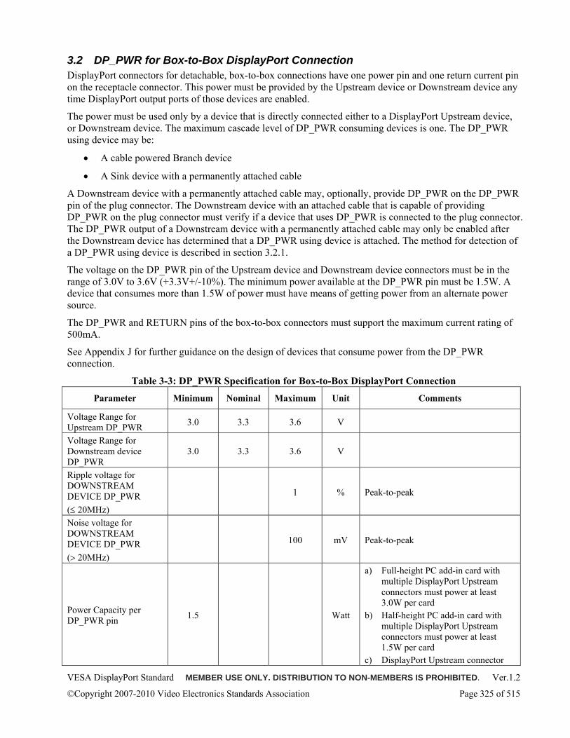
VESA DisplayPort Standard MEMBER USE ONLY. DISTRIBUTION TO NON-MEMBERS IS PROHIBITED. Ver.1.2
©Copyright 2007-2010 Video Electronics Standards Association Page 325 of 515
3.2 DP_PWR for Box-to-Box DisplayPort Connection DisplayPort connectors for detachable, box-to-box connections have one power pin and one return current pin on the receptacle connector. This power must be provided by the Upstream device or Downstream device any time DisplayPort output ports of those devices are enabled.
The power must be used only by a device that is directly connected either to a DisplayPort Upstream device, or Downstream device. The maximum cascade level of DP_PWR consuming devices is one. The DP_PWR using device may be:
• A cable powered Branch device
• A Sink device with a permanently attached cable
A Downstream device with a permanently attached cable may, optionally, provide DP_PWR on the DP_PWR pin of the plug connector. The Downstream device with an attached cable that is capable of providing DP_PWR on the plug connector must verify if a device that uses DP_PWR is connected to the plug connector. The DP_PWR output of a Downstream device with a permanently attached cable may only be enabled after the Downstream device has determined that a DP_PWR using device is attached. The method for detection of a DP_PWR using device is described in section 3.2.1.
The voltage on the DP_PWR pin of the Upstream device and Downstream device connectors must be in the range of 3.0V to 3.6V (+3.3V+/-10%). The minimum power available at the DP_PWR pin must be 1.5W. A device that consumes more than 1.5W of power must have means of getting power from an alternate power source.
The DP_PWR and RETURN pins of the box-to-box connectors must support the maximum current rating of 500mA.
See Appendix J for further guidance on the design of devices that consume power from the DP_PWR connection.
Table 3-3: DP_PWR Specification for Box-to-Box DisplayPort Connection
Parameter Minimum Nominal Maximum Unit Comments
Voltage Range for Upstream DP_PWR 3.0 3.3 3.6 V
Voltage Range for Downstream device DP_PWR
3.0 3.3 3.6 V
Ripple voltage for DOWNSTREAM DEVICE DP_PWR (≤ 20MHz)
1 % Peak-to-peak
Noise voltage for DOWNSTREAM DEVICE DP_PWR (> 20MHz)
100 mV Peak-to-peak
Power Capacity per DP_PWR pin 1.5 Watt
a) Full-height PC add-in card with multiple DisplayPort Upstream connectors must power at least 3.0W per card
b) Half-height PC add-in card with multiple DisplayPort Upstream connectors must power at least 1.5W per card
c) DisplayPort Upstream connector
VESA DisplayPort Standard MEMBER USE ONLY. DISTRIBUTION TO NON-MEMBERS IS PROHIBITED. Ver.1.2
©Copyright 2007-2010 Video Electronics Standards Association Page 326 of 515
on a PC motherboard must power 1.5W per connector regardless of the number of connectors on the motherboard.
3.2.1 DP_PWR User Detection Method Pins CONFIG1 and CONFIG2 of the box-to-box receptacle connector of DisplayPort Upstream and Downstream devices must be weakly pulled down with 1MΩ resistors.
Those two pins of a DisplayPort device with an Upstream function that uses power from DP_PWR must be shorted by a ≤ 100Ω resistor.
A Downstream Device with a permanently attached cable that is capable of supplying power on the DP_PWR pin of the plug connector must verify that pins CONFIG1 and CONFIG2 are shorted before enabling its DP_PWR output.
In order to detect the presence of a DP_PWR User, a Downstream device with a permanently attached cable must provide a probe power to Pin CONFIG2. If the Pin CONFIG1 voltage follows the probe power voltage applied to Pin CONFIG2, then, a DP_PWR User is present.
There will be a group of cable adaptors that pulls up Pin CONFIG1. Those cable adaptors with DisplayPort Receptacle connectors that pull up Pin CONFIG1 must not be a DP_PWR User. When a Downstream Device with a permanently attached cable detects H level on Pin CONFIG1 before providing a probe power to Pin CONFIG2, it determines that the attached cable adaptor is not a DP_PWR User
3.2.2 DP_PWR Wire A standard DisplayPort cable must have no wire for the DP_PWR pin.
Only captive cables supplied with cable powered Branch devices or cables permanently attached to Downstream devices or resizing adaptors or extension cables are permitted to have the wire for DP_PWR. These captive/attached/resizing/extension cables must have a full-size or mini DisplayPort plug connector (as specified in Section 4.2.1) on one end only. The other end must either be permanently attached or have a DisplayPort receptacle connector or have a custom connector.
3.2.3 Inrush Energy DisplayPort devices that consume DP_PWR must limit the inrush energy during Hot Plug to 0.4mJ, to be measured over the time period that the inrush exceeds 0.6A, and measured at 3.6V (the maximum voltage for DP_PWR). It is recommended that the peak current is limited to < 8A during the inrush energy window.
3.2.4 Voltage Droop DisplayPort Devices that provide power at DP_PWR pin should have sufficient bypass capacitor per DisplayPort connector be able to charge 56µF of low ESR capacitance plus 7.2Ω constant load across DP_PWR on hot plug of this load. Power provider devices should exhibit no obvious system failure and must ensure a voltage droop to no more than 10% of the normal DP_PWR supply voltage on any other DisplayPort connectors (measured at the connector) on the system on hot plug of this load.
3.2.5 Over-Current Protection End user accessible powered connectors must implement over-current protection for safety and regulatory reasons. Detection of an over-current condition and reporting this condition to the system software is optional and implementation-specific.
The preset trip limit must not exceed 3A at the Upstream device connector DP_PWR pin and 1.5A at the Downstream device connector DP_PWR pin. Limit must be above allowable current transients to avoid false trips. An over-current protection device must be resetable without user mechanical intervention.
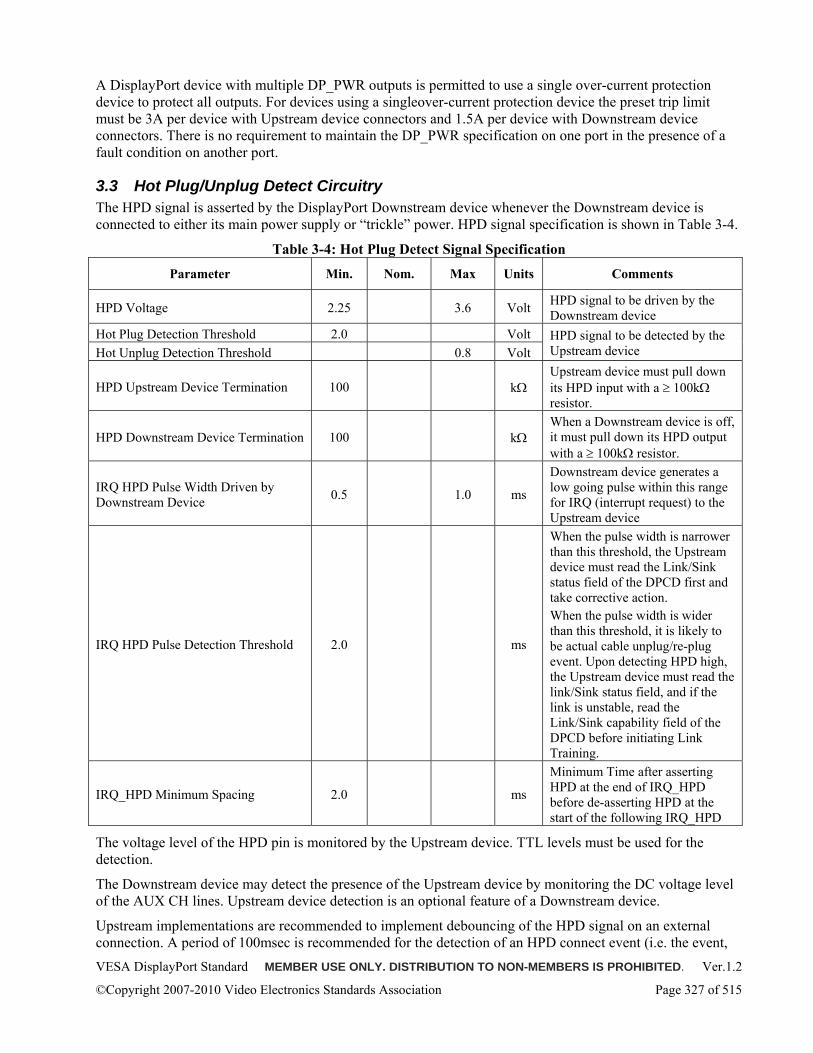
VESA DisplayPort Standard MEMBER USE ONLY. DISTRIBUTION TO NON-MEMBERS IS PROHIBITED. Ver.1.2
©Copyright 2007-2010 Video Electronics Standards Association Page 327 of 515
A DisplayPort device with multiple DP_PWR outputs is permitted to use a single over-current protection device to protect all outputs. For devices using a singleover-current protection device the preset trip limit must be 3A per device with Upstream device connectors and 1.5A per device with Downstream device connectors. There is no requirement to maintain the DP_PWR specification on one port in the presence of a fault condition on another port.
3.3 Hot Plug/Unplug Detect Circuitry The HPD signal is asserted by the DisplayPort Downstream device whenever the Downstream device is connected to either its main power supply or “trickle” power. HPD signal specification is shown in Table 3-4.
Table 3-4: Hot Plug Detect Signal Specification
Parameter Min. Nom. Max Units Comments
HPD Voltage 2.25 3.6 Volt HPD signal to be driven by the Downstream device
Hot Plug Detection Threshold 2.0 Volt Hot Unplug Detection Threshold 0.8 Volt
HPD signal to be detected by the Upstream device
HPD Upstream Device Termination 100
kΩ Upstream device must pull down its HPD input with a ≥ 100kΩ resistor.
HPD Downstream Device Termination 100
kΩ When a Downstream device is off, it must pull down its HPD output with a ≥ 100kΩ resistor.
IRQ HPD Pulse Width Driven by Downstream Device 0.5
1.0 ms
Downstream device generates a low going pulse within this range for IRQ (interrupt request) to the Upstream device
IRQ HPD Pulse Detection Threshold 2.0
ms
When the pulse width is narrower than this threshold, the Upstream device must read the Link/Sink status field of the DPCD first and take corrective action. When the pulse width is wider than this threshold, it is likely to be actual cable unplug/re-plug event. Upon detecting HPD high, the Upstream device must read the link/Sink status field, and if the link is unstable, read the Link/Sink capability field of the DPCD before initiating Link Training.
IRQ_HPD Minimum Spacing 2.0
ms
Minimum Time after asserting HPD at the end of IRQ_HPD before de-asserting HPD at the start of the following IRQ_HPD
The voltage level of the HPD pin is monitored by the Upstream device. TTL levels must be used for the detection.
The Downstream device may detect the presence of the Upstream device by monitoring the DC voltage level of the AUX CH lines. Upstream device detection is an optional feature of a Downstream device.
Upstream implementations are recommended to implement debouncing of the HPD signal on an external connection. A period of 100msec is recommended for the detection of an HPD connect event (i.e. the event,
VESA DisplayPort Standard MEMBER USE ONLY. DISTRIBUTION TO NON-MEMBERS IS PROHIBITED. Ver.1.2
©Copyright 2007-2010 Video Electronics Standards Association Page 328 of 515
"HPD high", is confirmed only after HPD has been asserted continuously for 100msec). Care should be taken not to implement debouncing on an HPD_IRQ and on a Downstream device-generated pair of HPD disconnect/reconnect events (typically HPD will be deasserted for more than 2msec but less than 100msec in this case). To cover these cases, it is recommended that the HPD debounce is only implemented after HPD low has been detected for 100msec. Timing requirements in this Standard related to the detection of HPD high are to be interpreted as applying from the completion of an implementation-dependent debounce period.
If the Downstream device has been placed a low power mode (see Section 5.1.5) but detects an event that it needs to notify to the Upstream device, then it asserts HPD_IRQ. The Upstream device will attempt to perform AUX transactions in order to wake the Downstream device. It is possible for the Upstream device already to be making AUX transactions to wake up the Downstream device. In this case, the Upstream device must complete the actions that it was already in process of execution (for example, waking the link and initiating training), and then perform appropriate DPCD register reads to ascertain the cause of the HPD_IRQ.
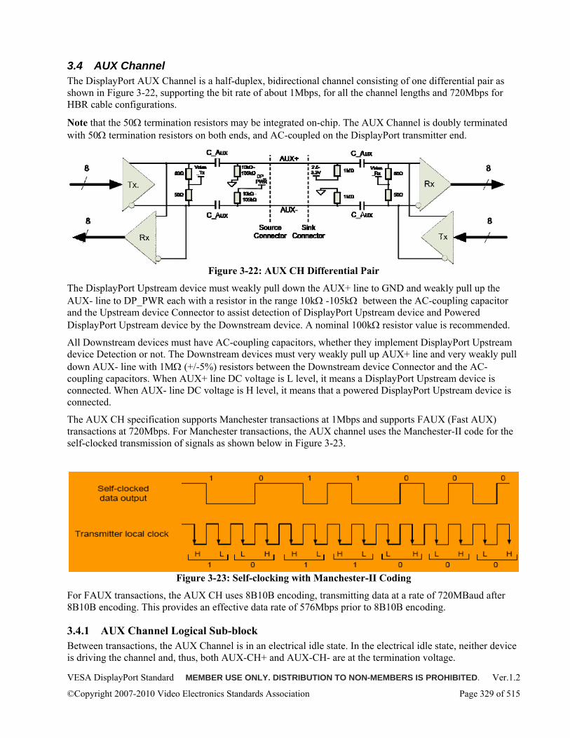
VESA DisplayPort Standard MEMBER USE ONLY. DISTRIBUTION TO NON-MEMBERS IS PROHIBITED. Ver.1.2
©Copyright 2007-2010 Video Electronics Standards Association Page 329 of 515
3.4 AUX Channel The DisplayPort AUX Channel is a half-duplex, bidirectional channel consisting of one differential pair as shown in Figure 3-22, supporting the bit rate of about 1Mbps, for all the channel lengths and 720Mbps for HBR cable configurations.
Note that the 50Ω termination resistors may be integrated on-chip. The AUX Channel is doubly terminated with 50Ω termination resistors on both ends, and AC-coupled on the DisplayPort transmitter end.
Figure 3-22: AUX CH Differential Pair
The DisplayPort Upstream device must weakly pull down the AUX+ line to GND and weakly pull up the AUX- line to DP_PWR each with a resistor in the range 10kΩ -105kΩ between the AC-coupling capacitor and the Upstream device Connector to assist detection of DisplayPort Upstream device and Powered DisplayPort Upstream device by the Downstream device. A nominal 100kΩ resistor value is recommended.
All Downstream devices must have AC-coupling capacitors, whether they implement DisplayPort Upstream device Detection or not. The Downstream devices must very weakly pull up AUX+ line and very weakly pull down AUX- line with 1MΩ (+/-5%) resistors between the Downstream device Connector and the AC-coupling capacitors. When AUX+ line DC voltage is L level, it means a DisplayPort Upstream device is connected. When AUX- line DC voltage is H level, it means that a powered DisplayPort Upstream device is connected.
The AUX CH specification supports Manchester transactions at 1Mbps and supports FAUX (Fast AUX) transactions at 720Mbps. For Manchester transactions, the AUX channel uses the Manchester-II code for the self-clocked transmission of signals as shown below in Figure 3-23.
Figure 3-23: Self-clocking with Manchester-II Coding
For FAUX transactions, the AUX CH uses 8B10B encoding, transmitting data at a rate of 720MBaud after 8B10B encoding. This provides an effective data rate of 576Mbps prior to 8B10B encoding.
3.4.1 AUX Channel Logical Sub-block Between transactions, the AUX Channel is in an electrical idle state. In the electrical idle state, neither device is driving the channel and, thus, both AUX-CH+ and AUX-CH- are at the termination voltage.
VESA DisplayPort Standard MEMBER USE ONLY. DISTRIBUTION TO NON-MEMBERS IS PROHIBITED. Ver.1.2
©Copyright 2007-2010 Video Electronics Standards Association Page 330 of 515
3.4.1.1 AUX Dual Mode Operation All DisplayPort devices must support Manchester transactions. Support for FAUX transactions is optional.
A Downstream device that supports FAUX transactions can operate either in Manchester Mode or in FAUX Mode, under the control of the Upstream device. If the Upstream device sets the Downstream device into Manchester Mode, then the Upstream device must not use FAUX transactions, and the Downstream device may place its FAUX circuitry into a low power state. If the Upstream device sets the Downstream device into FAUX Mode, then, once a delay has elapsed to allow the Downstream device to power up its FAUX circuitry, the Downstream device must be prepared to receive either Manchester or FAUX transactions at any time.
After an HPD connect event and after exit from display low-power mode (see Section 5.1.5), the Downstream device operates in Manchester Mode.
A Downstream device that supports FAUX transactions advertises this capability in the FAUX_CAP DPCD Register. A Upstream device that is FAUX transaction capable and that, as a matter of link policy, anticipates that it may use FAUX transactions, must inspect this capability before carrying out any other AUX transactions, and if it discovers that the connected Downstream device is also FAUX transaction capable, must use FAUX mode only as described in this section. The Upstream device controls whether the Downstream device is operating in Manchester Mode or FAUX Mode at any moment in time, according to its link policy
To switch the Downstream device from Manchester Mode to FAUX Mode, the Upstream device writes 0b1 to the FAUX_EN field in the FAUX_MODE_CTRL register using a 1-byte write Manchester transaction. Normally the other bits in the register will be written as zero at the same time. Exceptions are during training and compliance testing. The Downstream device must ACK the write, also using a Manchester transaction, and prepares to receive subsequent transactions as either Manchester or Faux transactions. The Downstream device must not transmit a NACK or an AUX_DEFER. The Upstream device must not use FAUX transactions until TFAUX_INITIALIZE has elapsed following receipt of the ACK. If the Upstream device does not receive a valid ACK (e.g. it receives an unrecognized response or times out), then it must retry the write of 0b1 to the FAUX_EN field in the FAUX_MODE_CTRL register using a Manchester transaction. Robustness beyond this is implementation dependent. However, if the Upstream device fails to switch to FAUX Mode, then it must perform a write of 0b0 to FAUX_EN using a Manchester transaction.
To switch the Downstream device from FAUX Mode to Manchester Mode, the Upstream device writes 0b0 to the FAUX_EN field in the FAUX_MODE_CTRL register using a 1-byte write (normally as a FAUX transaction). Normally the other bits in the register will be written as zero at the same time. Exceptions are during training and compliance testing. The Downstream device must ACK the write using the same transaction type as the original write. The Downstream device must not transmit a NACK or an AUX_DEFER. The next transaction from the Upstream device must be a Manchester transaction. The Downstream device may place its FAUX circuitry into a low power mode after completing the transmission of the ACK. If the Upstream device does not receive a valid ACK (e.g. it receives an unrecognized response or times out), then it must retry the write of 0b0 to the FAUX_EN field in the FAUX_MODE_CTRL register using a Manchester transaction (the initial assumption is that the ACK was corrupted). Robustness beyond this is implementation-dependent.
The Link Policy maker may decide to switch between Manchester Mode and FAUX Mode at any time.
The FAUX receiver must be capable of receiving a Manchester transaction at any time, including when it has been set into FAUX Mode.
3.4.1.2 Manchester Transactions AUX Channel transactions are initiated by the DisplayPort transmitter which acts as an AUX CH requester. The DisplayPort transmitter, which is the driving end for a request transaction, pre-charges the AUX-CH+ and AUX-CH- to a common mode voltage by transmitting 10 to 16 consecutive 0s in Manchester-II code.
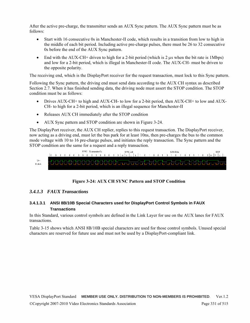
VESA DisplayPort Standard MEMBER USE ONLY. DISTRIBUTION TO NON-MEMBERS IS PROHIBITED. Ver.1.2
©Copyright 2007-2010 Video Electronics Standards Association Page 331 of 515
After the active pre-charge, the transmitter sends an AUX Sync pattern. The AUX Sync pattern must be as follows:
• Start with 16 consecutive 0s in Manchester-II code, which results in a transition from low to high in the middle of each bit period. Including active pre-charge pulses, there must be 26 to 32 consecutive 0s before the end of the AUX Sync pattern.
• End with the AUX-CH+ driven to high for a 2-bit period (which is 2 μs when the bit rate is 1Mbps) and low for a 2-bit period, which is illegal in Manchester-II code. The AUX-CH- must be driven to the opposite polarity.
The receiving end, which is the DisplayPort receiver for the request transaction, must lock to this Sync pattern.
Following the Sync pattern, the driving end must send data according to the AUX CH syntax as described Section 2.7. When it has finished sending data, the driving node must assert the STOP condition. The STOP condition must be as follows:
• Drives AUX-CH+ to high and AUX-CH- to low for a 2-bit period, then AUX-CH+ to low and AUX-CH- to high for a 2-bit period, which is an illegal sequence for Manchester-II
• Releases AUX CH immediately after the STOP condition
• AUX Sync pattern and STOP condition are shown in Figure 3-24.
The DisplayPort receiver, the AUX CH replier, replies to this request transaction. The DisplayPort receiver, now acting as a driving end, must let the bus park for at least 10ns, then pre-charges the bus to the common mode voltage with 10 to 16 pre-charge pulses, and initiates the reply transaction. The Sync pattern and the STOP condition are the same for a request and a reply transaction.
Figure 3-24: AUX CH SYNC Pattern and STOP Condition
3.4.1.3 FAUX Transactions
3.4.1.3.1 ANSI 8B/10B Special Characters used for DisplayPort Control Symbols in FAUX Transactions
In this Standard, various control symbols are defined in the Link Layer for use on the AUX lanes for FAUX transactions.
Table 3-15 shows which ANSI 8B/10B special characters are used for those control symbols. Unused special characters are reserved for future use and must not be used by a DisplayPort-compliant link.
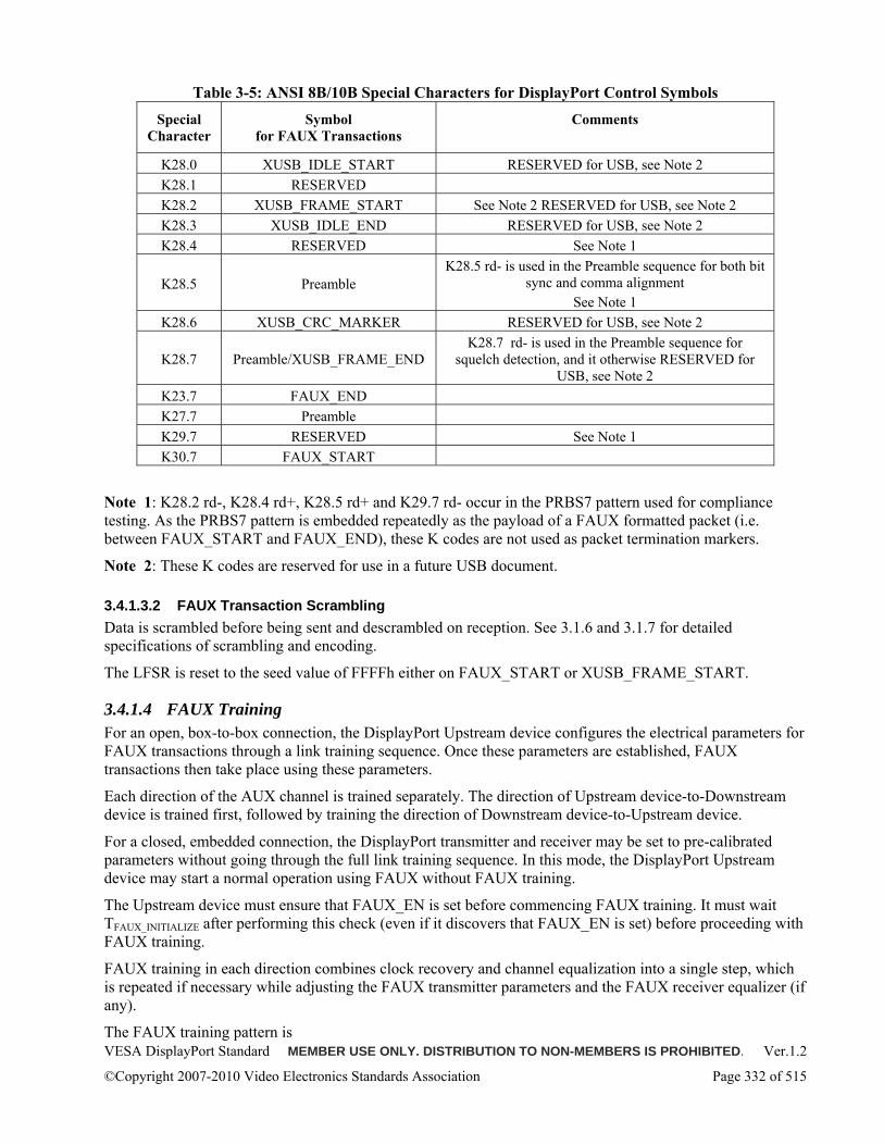
VESA DisplayPort Standard MEMBER USE ONLY. DISTRIBUTION TO NON-MEMBERS IS PROHIBITED. Ver.1.2
©Copyright 2007-2010 Video Electronics Standards Association Page 332 of 515
Table 3-5: ANSI 8B/10B Special Characters for DisplayPort Control Symbols
Special Character
Symbol for FAUX Transactions
Comments
K28.0 XUSB_IDLE_START RESERVED for USB, see Note 2 K28.1 RESERVED K28.2 XUSB_FRAME_START See Note 2 RESERVED for USB, see Note 2 K28.3 XUSB_IDLE_END RESERVED for USB, see Note 2 K28.4 RESERVED See Note 1
K28.5 Preamble K28.5 rd- is used in the Preamble sequence for both bit
sync and comma alignment See Note 1
K28.6 XUSB_CRC_MARKER RESERVED for USB, see Note 2
K28.7 Preamble/XUSB_FRAME_END K28.7 rd- is used in the Preamble sequence for
squelch detection, and it otherwise RESERVED for USB, see Note 2
K23.7 FAUX_END K27.7 Preamble K29.7 RESERVED See Note 1 K30.7 FAUX_START
Note 1: K28.2 rd-, K28.4 rd+, K28.5 rd+ and K29.7 rd- occur in the PRBS7 pattern used for compliance testing. As the PRBS7 pattern is embedded repeatedly as the payload of a FAUX formatted packet (i.e. between FAUX_START and FAUX_END), these K codes are not used as packet termination markers.
Note 2: These K codes are reserved for use in a future USB document.
3.4.1.3.2 FAUX Transaction Scrambling Data is scrambled before being sent and descrambled on reception. See 3.1.6 and 3.1.7 for detailed specifications of scrambling and encoding.
The LFSR is reset to the seed value of FFFFh either on FAUX_START or XUSB_FRAME_START.
3.4.1.4 FAUX Training For an open, box-to-box connection, the DisplayPort Upstream device configures the electrical parameters for FAUX transactions through a link training sequence. Once these parameters are established, FAUX transactions then take place using these parameters.
Each direction of the AUX channel is trained separately. The direction of Upstream device-to-Downstream device is trained first, followed by training the direction of Downstream device-to-Upstream device.
For a closed, embedded connection, the DisplayPort transmitter and receiver may be set to pre-calibrated parameters without going through the full link training sequence. In this mode, the DisplayPort Upstream device may start a normal operation using FAUX without FAUX training.
The Upstream device must ensure that FAUX_EN is set before commencing FAUX training. It must wait TFAUX_INITIALIZE after performing this check (even if it discovers that FAUX_EN is set) before proceeding with FAUX training.
FAUX training in each direction combines clock recovery and channel equalization into a single step, which is repeated if necessary while adjusting the FAUX transmitter parameters and the FAUX receiver equalizer (if any).
The FAUX training pattern is
VESA DisplayPort Standard MEMBER USE ONLY. DISTRIBUTION TO NON-MEMBERS IS PROHIBITED. Ver.1.2
©Copyright 2007-2010 Video Electronics Standards Association Page 333 of 515
K28.1+, K27.7-, K28.1-, K27.7+
and is repeated for at least TRAINING_AUX_RD_INTERVAL (Forward Channel training) or FAUX_BACK_CHANNEL_TRAINING_PATTERN_TIME (Back Channel training), as specified by the receiving device.
The training sequence is initiated by the Link Policy Maker in the Upstream device after detecting an HPD connect event. When the Upstream device detects the HDP low-high transition at the end of an HPD low-going pulse that exceeds 2 ms in width, the Link Policy Maker must read the link capability field of the DPCD via the AUX CH. If the Link Policy Maker determines that the Downstream device is FAUX-capable, it initiates FAUX training. It first performs Upstream device-to-Downstream device training, and then performs Downstream device-to-Upstream device training.
All DPCD reads and writes during FAUX training are conducted using Manchester transactions.
After initial connection or after exit from a low power state, FAUX training must precede main link training. This is to allow FAUX transactions to run in parallel with main link training for crosstalk compensation purposes.
Note that the link policy maker may place or maintain the main link into a low power state whilst maintaining the AUX connection in a fully operational state running Manchester and/or FAUX transactions.
3.4.1.4.1 FAUX Forward Channel Training The Link Policy Maker must start the FAUX Link Training by reading TRAINING_AUX_RD_INTERVAL to determine the minimum duration of each transmission of the training pattern, and ensuring that FAUX_EN is set. It then must commence Upstream device-to-Downstream device (Forward Channel) training by writing appropriate values to FAUX_FORWARD_CHANNEL_VOLTAGE_SWING_SET, FAUX_FORWARD_CHANNEL_PRE-EMPHASIS_SET, FAUX_FORWARD_CHANNEL_MAX_SWING_REACHED and FAUX_FORWARD_CHANNEL_MAX_PRE-EMPHASIS_REACHED.
At the start of FAUX training, the Upstream device must start signaling at voltage swing level 0, pre-emphasis level 0.
Note: The Upstream device may start with non-minimum differential voltage swing and with pre-emphasis if the optimal setting is already known, for example, as is the case in embedded application.
The Upstream device then primes the Downstream device to prepare to receive the training pattern by setting FAUX_FORWARD_CHANNEL_TRAINING_PATTERN_EN and FAUX_SCRAMBLER_DIS (scrambling is disabled during training). The Downstream device replies to this transaction with ACK, and after receiving the ACK the Upstream device waits AUX Park time and then sends the training pattern for at least TRAINING_AUX_RD_INTERVAL.
The Downstream device must attempt to achieve frequency and symbol lock while receiving this pattern. The Downstream device sets the FAUX_FORWARD_CHANNEL_SYMBOL_LOCK_DONE bit in DPCD Link Status field only when its link CDR (clock and data recovery) unit has realized and maintained the frequency lock and its receiver has properly detected and aligned the ANSI8B/10B symbol boundaries and set its internal equalizer (if any). The receiver must use the recognition of the training pattern to decide whether the channel equalization is successful or not. How to measure the equalization result is implementation-specific.
Given the bit error rate target of 1E-12 and the duration of the link training period (10ms or less), the receiver should detect no more than a single symbol error during the link training to set the FAUX_FORWARD_CHANNEL_SYMBOL_LOCK_DONE bit. For optimizing the drive setting of the DisplayPort transmitter, the receiver may defer setting FAUX_FORWARD_CHANNEL_SYMBOL_LOCK_DONE bits until the optimization is completed.
VESA DisplayPort Standard MEMBER USE ONLY. DISTRIBUTION TO NON-MEMBERS IS PROHIBITED. Ver.1.2
©Copyright 2007-2010 Video Electronics Standards Association Page 334 of 515
If the Downstream device fails to achieve frequency lock and symbol lock, the Downstream device must keep the FAUX_FORWARD_CHANNEL_SYMBOL_LOCK_DONE bit cleared and request an increase of the differential voltage swing and/or pre-emphasis by updating the value in FAUX_FORWARD_CHANNEL_VOLTAGE_SWING_ADJ_REQ and FAUX_FORWARD_CHANNEL_PRE-EMPHASIS_ADJ_REQ bits.
After at least TRAINING_AUX_RD_INTERVAL has elapsed, the Upstream device stops transmitting the training pattern, and reads the results of training from the Downstream device, i.e. FAUX_FORWARD_CHANNEL_SYMBOL_LOCK_DONE, FAUX_FORWARD_CHANNEL_VOLTAGE_SWING_ADJ_REQ and FAUX_FORWARD_CHANNEL_PRE-EMPHASIS_ADJ_REQ.
If FAUX_FORWARD_CHANNEL_SYMBOL_LOCK_DONE is not set, the Upstream device must make the requested adjustments to the drive settings, set appropriate values to FAUX_FORWARD_CHANNEL_VOLTAGE_SWING_SET, FAUX_FORWARD_CHANNEL_PRE-EMPHASIS_SET, FAUX_FORWARD_CHANNEL_MAX_SWING_REACHED and FAUX_FORWARD_CHANNEL_MAX_PRE-EMPHASIS_REACHED, set FAUX_FORWARD_CHANNEL_TO_SINK_TRAINING_PATTERN_EN and FAUX_SCRAMBLER_DIS, wait for the Downstream device to send the ACK and then re-send the training pattern for at least TRAINING_AUX_RD_INTERVAL, repeating the process described above.
A DisplayPort receiver must issue a drive setting adjustment request within the limit defined in this Standard.
If the Downstream device keeps the same value in FAUX_FORWARD_CHANNEL_VOLTAGE_SWING_ADJ_REQ and FAUX_FORWARD_CHANNEL_PRE-EMPHASIS_ADJ_REQ while FAUX_FORWARD_CHANNEL_SYMBOL_LOCK_DONE bits remain unset, the Link Policy Maker must loop four times with the same voltage swing. On the 5th unsuccessful time, the Link Policy Maker must end the training (by clearing the FAUX_MODE_CTRL byte to 00h in the DPCD) and use only Manchester Mode.
Once it reads FAUX_FORWARD_CHANNEL_SYMBOL_LOCK_DONE bit as being set, the Link Policy Maker must move on to Downstream device-to-Upstream device training. The Link Policy Maker must use the results of training for all FAUX transmissions from the Upstream device to the Downstream device. The Downstream device must maintain FAUX_FORWARD_CHANNEL_SYMBOL_LOCK_DONE, except to request re-training of FAUX and when the Upstream device initially sets FAUX_FORWARD_CHANNEL_TRAINING_PATTERN_EN at the start of any re-training. The Downstream device must not clear FAUX_FORWARD_CHANNEL_SYMBOL_LOCK_DONE if the Link Policy Maker decides to switch to Manchester Mode (by clearing FAUX_EN).
The FAUX Upstream device-to-Downstream device training algorithm is shown in Figure 3-32.
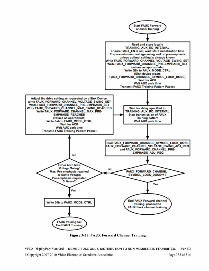
VESA DisplayPort Standard MEMBER USE ONLY. DISTRIBUTION TO NON-MEMBERS IS PROHIBITED. Ver.1.2
©Copyright 2007-2010 Video Electronics Standards Association Page 335 of 515
Figure 3-25: FAUX Forward Channel Training
VESA DisplayPort Standard MEMBER USE ONLY. DISTRIBUTION TO NON-MEMBERS IS PROHIBITED. Ver.1.2
©Copyright 2007-2010 Video Electronics Standards Association Page 336 of 515
3.4.1.4.2 FAUX Back Channel Training During FAUX Back Channel training after initial connection, or after exit from a low power state or at any time when the main link is not trained and active, the main link may transmit aggressor traffic, recommended to comprise a continuous sequence of unscrambled D10.2 symbols, on all supported lanes at an implementation-dependent implemented voltage swing and pre-emphasis level and at an implementation- dependent speed not to exceed the fastest speed of which the Downstream port is capable. If the main link is trained and active, but not using all available lanes, then the main link may transmit aggressor traffic as specified above on all otherwise unused lanes. This is to ensure that any signal degradation due to crosstalk between the main link and the AUX lines when receiving a FAUX signal is compensated for during FAUX training. The Downstream port must ensure that it ignores the main link aggressor traffic if present.
At the start of FAUX Downstream device-to-Upstream device (Back Channel) training, the Downstream device must start signaling at voltage swing level 0, pre-emphasis level 0. The Downstream device must set appropriate values to FAUX_BACK_CHANNEL_VOLTAGE_SWING_SET, FAUX_BACK_CHANNEL_PRE-EMPHASIS_SET, FAUX_BACK_CHANNEL_MAX_SWING_REACHED and FAUX_BACK_CHANNEL_MAX_PRE-EMPHASIS_REACHED.
Note: The Downstream device may start with non-minimum differential voltage swing and with pre-emphasis if the optimal setting is already known, for example, as is the case in embedded application.
The Link Policy Maker must commence Downstream device-to-Upstream device training by reading the Downstream device's values for FAUX_BACK_CHANNEL_VOLTAGE_SWING_SET, FAUX_BACK_CHANNEL_PRE-EMPHASIS_SET, FAUX_BACK_CHANNEL_MAX_SWING_REACHED and FAUX_BACK_CHANNEL_MAX_PRE-EMPHASIS_REACHED.
The Upstream device then requests the Downstream device to transmit the training pattern by setting FAUX_BACK_CHANNEL_TRAINING_PATTERN_TIME, FAUX_BACK_CHANNEL_TRAINING_PATTERN_EN and FAUX_SCRAMBLER_DIS (scrambling is disabled during training). The Downstream device replies to this transaction with ACK, and after waiting AUX Park time it sends the training pattern for at least FAUX_BACK_CHANNEL_TRAINING_PATTERN_TIME. After a period of time no less than FAUX_BACK_CHANNEL_TRAINING_PATTERN_TIME has elapsed, the Downstream device stops transmitting the training pattern.
The Upstream device must attempt to achieve frequency and symbol lock while receiving this pattern. It achieves this only when its link CDR (clock and data recovery) unit has realized and maintained the frequency lock and its AUX receiver has properly detected and aligned the ANSI8B/10B symbol boundaries and set its internal equalizer (if any). The AUX receiver must use the recognition of the training pattern to decide whether the channel equalization is successful or not. How to measure the equalization result is implementation-specific.
Given the bit error rate target of 1E-12 and the duration of the link training period (10ms or less), the receiver should detect no more than a single symbol error during the link training. For optimizing the drive setting of the DisplayPort transmitter, the Upstream device may defer setting FAUX_BACK_CHANNEL_SYMBOL_LOCK_DONE bits until the optimization is completed.
If the Upstream device fails to achieve frequency lock and symbol lock, it must keep the FAUX_BACK_CHANNEL_SYMBOL_LOCK_DONE bit cleared and request an increase of the differential voltage swing and/or pre-emphasis by updating the value in FAUX_BACK_CHANNEL_VOLTAGE_SWING_ADJ_REQ and FAUX_BACK_CHANNEL_PRE-EMPHASIS_ADJ_REQ bits.
If FAUX_BACK_CHANNEL_SYMBOL_LOCK_DONE is not set, the Downstream device must make the requested adjustments to the drive settings, set appropriate values to
VESA DisplayPort Standard MEMBER USE ONLY. DISTRIBUTION TO NON-MEMBERS IS PROHIBITED. Ver.1.2
©Copyright 2007-2010 Video Electronics Standards Association Page 337 of 515
FAUX_BACK_CHANNEL_VOLTAGE_SWING_SET, FAUX_BACK_CHANNEL_PRE-EMPHASIS_SET, FAUX_BACK_CHANNEL_MAX_SWING_REACHED and FAUX_BACK_CHANNEL_MAX_PRE-EMPHASIS_REACHED. The Upstream device reads these values, and requests the Downstream device to re-send the training pattern by setting FAUX_BACK_CHANNEL_TRAINING_PATTERN_EN and FAUX_SCRAMBLER_DIS. The Downstream device replies to this transaction with ACK, and after waiting AUX Park time it sends the training pattern for at least FAUX_BACK_CHANNEL_TRAINING_PATTERN_TIME. repeating the process described above.
A DisplayPort Upstream device must issue a drive setting adjustment request within the limit defined in DisplayPort Standard Ver.1.1.
If the Link Policy Maker is unable to achieve full synchronization it may loop up to four times with the same voltage swing. On the 5th time, the Link Policy Maker must end the training (by clearing the FAUX_MODE_CTRL byte to 00h in the DPCD) and use only Manchester Mode.
Once the Upstream device achieves frequency and symbol lock, it must set FAUX_BACK_CHANNEL_SYMBOL_LOCK_DONE. The Downstream device must use the results of training for all FAUX transmissions from the Upstream device to the Downstream device. The Link Policy Maker must not clear FAUX_BACK_CHANNEL_SYMBOL_LOCK_DONE if it decides to switch to Manchester Mode (by clearing FAUX_EN).
At any time after completion of training, the Link Policy Maker in the Upstream device may decide to stop using FAUX Mode by clearing FAUX_EN.
The FAUX Downstream device-to-Upstream device training algorithm is shown in Figure 3-33.
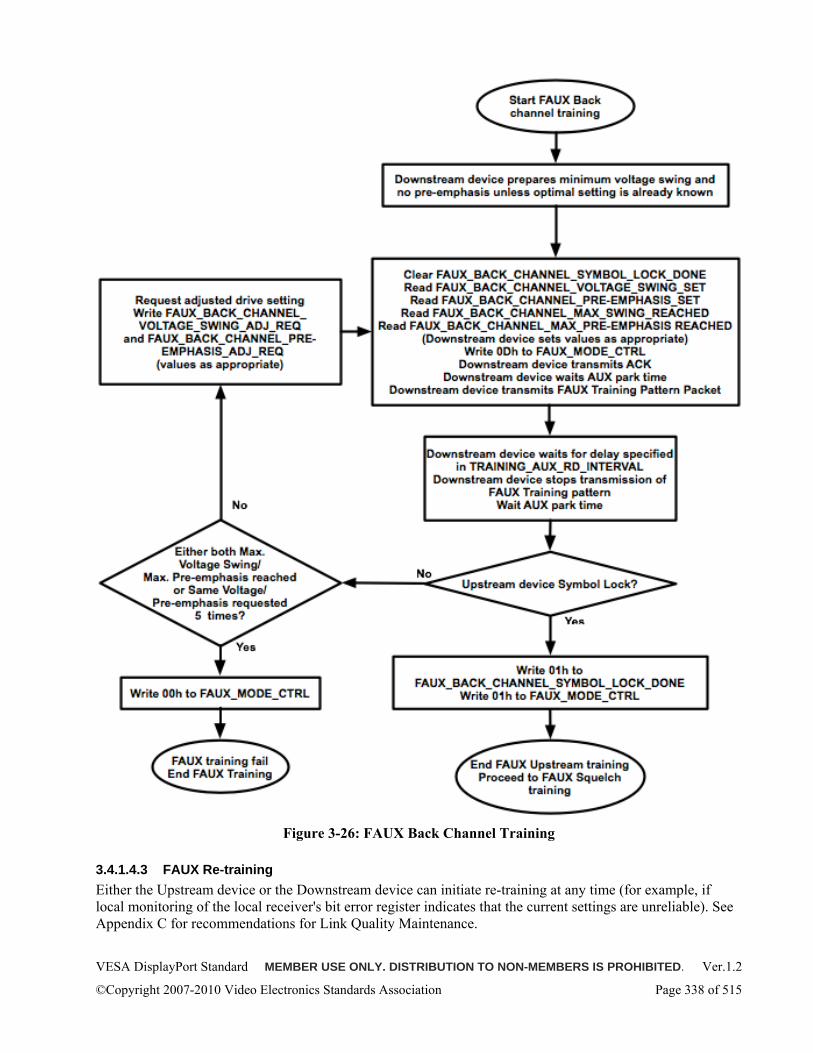
VESA DisplayPort Standard MEMBER USE ONLY. DISTRIBUTION TO NON-MEMBERS IS PROHIBITED. Ver.1.2
©Copyright 2007-2010 Video Electronics Standards Association Page 338 of 515
Figure 3-26: FAUX Back Channel Training
3.4.1.4.3 FAUX Re-training Either the Upstream device or the Downstream device can initiate re-training at any time (for example, if local monitoring of the local receiver's bit error register indicates that the current settings are unreliable). See Appendix C for recommendations for Link Quality Maintenance.
VESA DisplayPort Standard MEMBER USE ONLY. DISTRIBUTION TO NON-MEMBERS IS PROHIBITED. Ver.1.2
©Copyright 2007-2010 Video Electronics Standards Association Page 339 of 515
When the Upstream device initiates re-training, it must clear FAUX_BACK_CHANNEL_SYMBOL_LOCK_DONE.
When the Downstream device initiates re-training, it must clear FAUX_FORWARD_CHANNEL_SYMBOL_LOCK_DONE and generate an HPD_IRQ. The Downstream device autonomously switches to Manchester Mode. The Link Policy Maker must detect that FAUX_FORWARD_CHANNEL_SYMBOL_LOCK_DONE has been cleared by attempting to read FAUX_FORWARD_CHANNEL_STATUS. It will normally use a FAUX transaction to do this, in which case the transaction will fail, and so it must repeat the read using a Manchester transaction.
3.4.1.5 Protocol Assisted Squelch Feature The FAUX preamble pattern consists of leading K28.7s for "squelch" detection (i.e. the detection of the presence of active signaling, squelching any noise that may be detectable when signaling is not present), followed by D10.2s and K28.5s for phase alignment and symbol alignment respectively.
Upon link idle, the squelch detector is responsible for electrically detecting the start of a preamble. Because the K28.7 symbol contains 5 consecutive 0s and 5 consecutive 1s, the overall signal amplitude reaching the receiving silicon at the end of the long run-length is larger than the minimum FAUX link EYE height. When squelch is detected by the receiver, the receiving silicon must wake up its receiving logic to lock to the preamble pattern and keep the receive circuits in full operation until the FAUX protocol declares an end of transmission (i.e. the output of the squelch detector is disregarded during packet reception). In this respect, the squelch detector is responsible for wakeup of the receive logic, while the power-down of the receive logic is performed by FAUX protocol in complement.
3.4.1.5.1 Squelch Detection Requirement An Upstream device is not required to implement squelch detection, as an Upstream device is always the requester and therefore can be prepared to receive a prompt response to a request that it issues. (A Downstream device cannot directly initiate an AUX transaction, but can toggle the HPD line to prompt the Upstream device to initiate an AUX request transaction.) However, an Upstream device must implement protocol features to enable possible downstream squelch implementations.
If a Downstream device chooses to implement squelch detection, the delays in reply to a request transaction from an Upstream device depends on the FAUX Power State. The Downstream device FAUX Power States are defined as the following:
1. FAUX Power State 1 (FASP1): Active
The Downstream device is waiting for FAUX request transaction from an Upstream device and ready to reply within Response Time-Out period (=0.6us in FAUX mode)
2. FAUX Power State 2 (FASP2): Standby
The Downstream device enters into standby state after receiving no FAUX request transaction for one second or longer. The Downstream device would keep its squelch detection circuits enabled, and restore its FAUX circuitry back to active state within 2us on detecting an incoming signal. In the case of no reply for Reply Time-Out period (1us in FAUX mode), an Upstream device is to retry at least three times.
3. FAUX Power State 3 (FASP3): FAUX disabled
The Downstream device enters the FAUX disabled state when the Upstream Link Policy Maker clears FAUX_EN. The Upstream Link Policy Maker re-enables FAUX by setting FAUX_EN (using a Manchester transaction). The Downstream device must transition to FASP1 within TFAUX_INITIALIZE
4. FAUX Power State 4 (FASP4): Sleep
VESA DisplayPort Standard MEMBER USE ONLY. DISTRIBUTION TO NON-MEMBERS IS PROHIBITED. Ver.1.2
©Copyright 2007-2010 Video Electronics Standards Association Page 340 of 515
The Upstream device puts the Downstream device in Sleep state by writing 02h to DPCD address 00600h. The Downstream device must keep its squelch detection circuits enabled and be able to restore its FAUX circuitry back to active state within 1ms.
With the above FAUX state definitions, there are two modes of FAUX for a Downstream device; squelch detect mode or high sensitivity mode.
The squelch detect mode refers to FAS2, FAS3 and FAS4, which are power-save states. The high sensitivity mode is entered after squelch detection circuit detects squelch, and transitions to FAS1 (active state) and stays in high sensitivity mode while in FAS1.
3.4.1.5.2 Squelch Detection Training Pattern Squelch detection training must be initiated immediately follow FAUX link training, with handshaking performed using Manchester-II transactions. The training pattern consists of a repetition of transmission of the pre-amble sequence for 20us by the Upstream device, followed by no transmission for 20us, at the voltage swing and pre-emphasis levels determined during FAUX Forward Channel training. This 20us + 20us sequence is repeated until the Downstream device indicates “Squelch Threshold Done” status.
The Upstream device first sets FAUX_DOWNSTREAM_SQUELCH_TRAINING_EN in the FAUX_MODE_CONTROL DPCD register using a Manchester transaction, then, on receipt of the ACK, transmits the training pattern for a minimum of 500μs, then reads FAUX_ FORWARD_CHANNEL _SQUELCH_THRESHOLD_DONE from the FAUX_FORWARD_CHANNEL_STATUS DPCD register using a Manchester transaction. If this status bit is set, then squelch training is complete. If this bit is not set, then the Upstream device repeats the squelch training pattern for a further 500us and then repeats the status read. If the training pattern is transmitted five times without the status bit being set, then the Upstream device must not use FAUX transactions and must clear FAUX_EN for the duration of the connection.
3.4.1.6 FAUX Packet Transmission The FAUX packet has the general format
<Preamble>repeated 12 times<FAUX_START | XUSB_FRAME_START ><payload symbol*> <FAUX_END | XUSB_FRAME_END >
The twelve Preamble symbols comprise two K28.7 control symbols transmitted with negative disparity, followed by four D10.2 data symbols transmitted with negative disparity, followed by six K28.5 control symbols, starting at negative disparity, i.e.
K28.7-, K28.7-, D10.2-, D10.2-, D10.2-, D10.2-, K28.5-, K28.5+, K28.5-, K28.5+, K28.5-, K28.5+
The initial two K28.7 symbols are provided to assist squelch detection at the receiver, i.e. detecting the presence of a valid signal that "squelches" any noise that may be present when no signal is being transmitted. Note that this intentionally breaks the 8B10B rule prohibiting consecutive K28.7 symbols, and that the two K28.7- symbols should not be relied upon for symbol alignment (symbol alignment should be established based on the K28.5 symbols later in the preamble).
The format places no limit on the number of payload symbols. Each payload symbol is a scrambled data symbol or one of the unscrambled special symbols used as a USB delimiter (XUSB_IDLE_START, XUSB_IDLE_END or XUSB_CRC_MARKER). The format of the FAUX packet payload is defined in Section 2.8.
For compliance purposes, a special packet is constructed in which the payload symbols are replaced by a PRBS7 bit pattern repeated enough times so that the packet duration is approximately 30 seconds. As the PRBS7 pattern contains 127 bits, it must be repeated a multiple of 10 times so that the FAUX_END symbol is correctly aligned.
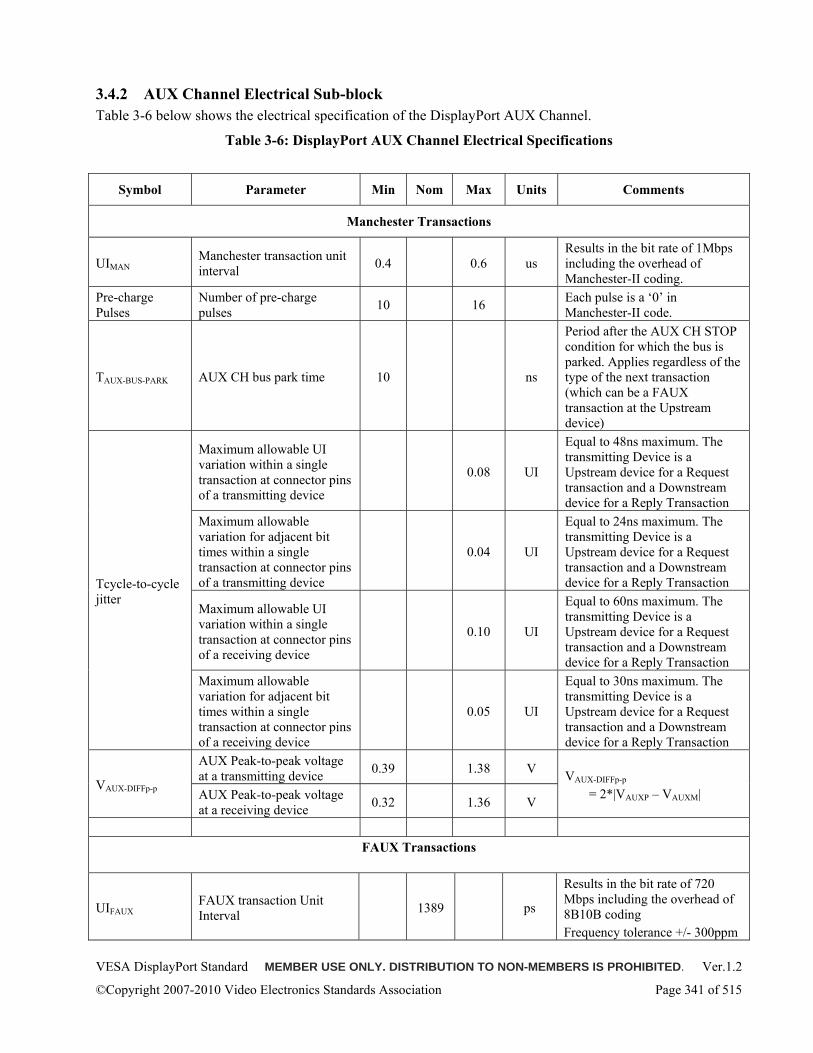
VESA DisplayPort Standard MEMBER USE ONLY. DISTRIBUTION TO NON-MEMBERS IS PROHIBITED. Ver.1.2
©Copyright 2007-2010 Video Electronics Standards Association Page 341 of 515
3.4.2 AUX Channel Electrical Sub-block Table 3-6 below shows the electrical specification of the DisplayPort AUX Channel.
Table 3-6: DisplayPort AUX Channel Electrical Specifications
Symbol Parameter Min Nom Max Units Comments
Manchester Transactions
UIMAN Manchester transaction unit interval 0.4 0.6 us
Results in the bit rate of 1Mbps including the overhead of Manchester-II coding.
Pre-charge Pulses
Number of pre-charge pulses 10 16 Each pulse is a ‘0’ in
Manchester-II code.
TAUX-BUS-PARK AUX CH bus park time 10 ns
Period after the AUX CH STOP condition for which the bus is parked. Applies regardless of the type of the next transaction (which can be a FAUX transaction at the Upstream device)
Maximum allowable UI variation within a single transaction at connector pins of a transmitting device
0.08 UI
Equal to 48ns maximum. The transmitting Device is a Upstream device for a Request transaction and a Downstream device for a Reply Transaction
Maximum allowable variation for adjacent bit times within a single transaction at connector pins of a transmitting device
0.04 UI
Equal to 24ns maximum. The transmitting Device is a Upstream device for a Request transaction and a Downstream device for a Reply Transaction
Maximum allowable UI variation within a single transaction at connector pins of a receiving device
0.10 UI
Equal to 60ns maximum. The transmitting Device is a Upstream device for a Request transaction and a Downstream device for a Reply Transaction
Tcycle-to-cycle jitter
Maximum allowable variation for adjacent bit times within a single transaction at connector pins of a receiving device
0.05 UI
Equal to 30ns maximum. The transmitting Device is a Upstream device for a Request transaction and a Downstream device for a Reply Transaction
AUX Peak-to-peak voltage at a transmitting device 0.39 1.38 V
VAUX-DIFFp-p AUX Peak-to-peak voltage at a receiving device 0.32 1.36 V
VAUX-DIFFp-p = 2*|VAUXP – VAUXM|
FAUX Transactions
UIFAUX FAUX transaction Unit Interval 1389 ps
Results in the bit rate of 720 Mbps including the overhead of 8B10B coding Frequency tolerance +/- 300ppm
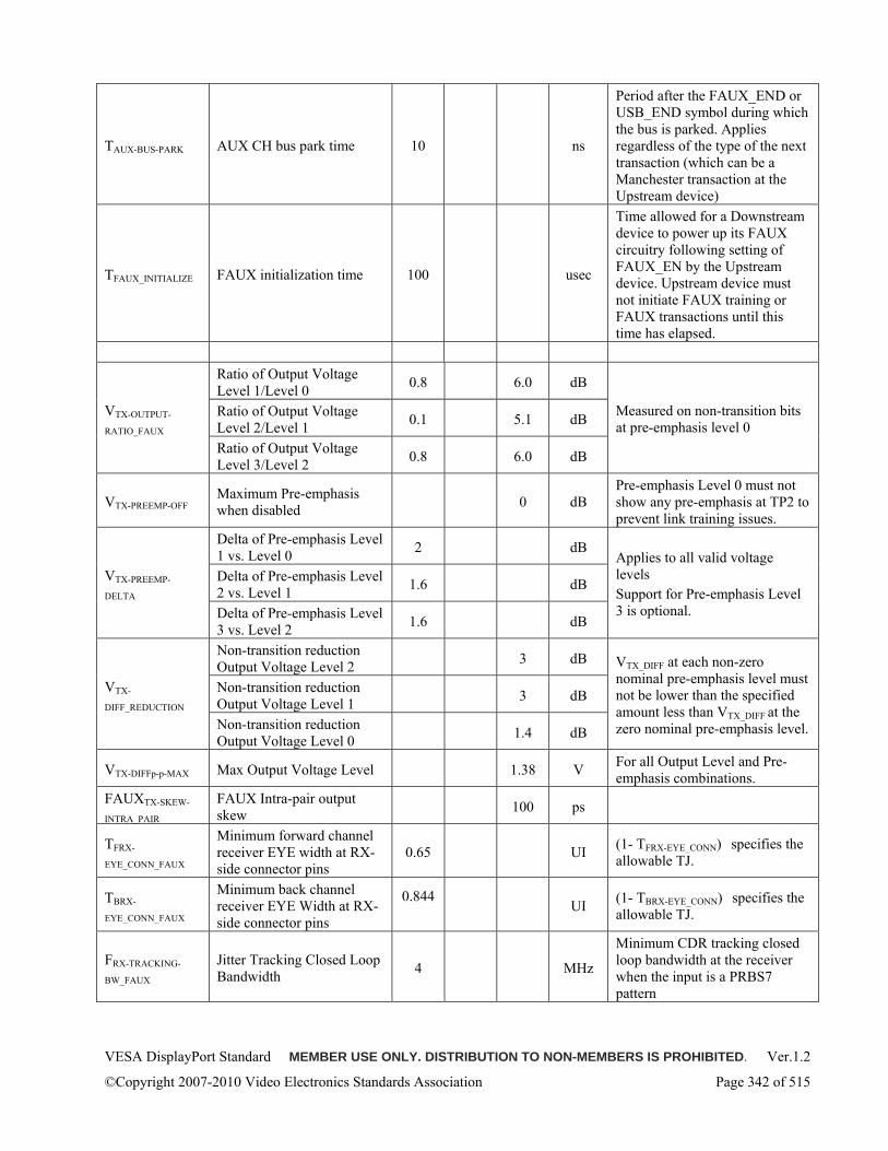
VESA DisplayPort Standard MEMBER USE ONLY. DISTRIBUTION TO NON-MEMBERS IS PROHIBITED. Ver.1.2
©Copyright 2007-2010 Video Electronics Standards Association Page 342 of 515
TAUX-BUS-PARK AUX CH bus park time 10 ns
Period after the FAUX_END or USB_END symbol during which the bus is parked. Applies regardless of the type of the next transaction (which can be a Manchester transaction at the Upstream device)
TFAUX_INITIALIZE FAUX initialization time 100 usec
Time allowed for a Downstream device to power up its FAUX circuitry following setting of FAUX_EN by the Upstream device. Upstream device must not initiate FAUX training or FAUX transactions until this time has elapsed.
Ratio of Output Voltage Level 1/Level 0 0.8 6.0 dB
Ratio of Output Voltage Level 2/Level 1 0.1 5.1 dB VTX-OUTPUT-
RATIO_FAUX Ratio of Output Voltage Level 3/Level 2 0.8 6.0 dB
Measured on non-transition bits at pre-emphasis level 0
VTX-PREEMP-OFF Maximum Pre-emphasis when disabled 0 dB
Pre-emphasis Level 0 must not show any pre-emphasis at TP2 to prevent link training issues.
Delta of Pre-emphasis Level 1 vs. Level 0 2 dB
Delta of Pre-emphasis Level 2 vs. Level 1 1.6 dB VTX-PREEMP-
DELTA Delta of Pre-emphasis Level 3 vs. Level 2 1.6 dB
Applies to all valid voltage levels Support for Pre-emphasis Level 3 is optional.
Non-transition reduction Output Voltage Level 2 3 dB
Non-transition reduction Output Voltage Level 1 3 dB VTX-
DIFF_REDUCTION Non-transition reduction Output Voltage Level 0 1.4 dB
VTX_DIFF at each non-zero nominal pre-emphasis level must not be lower than the specified amount less than VTX_DIFF at the zero nominal pre-emphasis level.
VTX-DIFFp-p-MAX Max Output Voltage Level 1.38 V For all Output Level and Pre-emphasis combinations.
FAUXTX-SKEW-
INTRA_PAIR FAUX Intra-pair output skew 100 ps
TFRX-
EYE_CONN_FAUX
Minimum forward channel receiver EYE width at RX-side connector pins
0.65 UI (1- TFRX-EYE_CONN) specifies the allowable TJ.
TBRX-
EYE_CONN_FAUX
Minimum back channel receiver EYE Width at RX-side connector pins
0.844
UI (1- TBRX-EYE_CONN) specifies the allowable TJ.
FRX-TRACKING-
BW_FAUX Jitter Tracking Closed Loop Bandwidth 4 MHz
Minimum CDR tracking closed loop bandwidth at the receiver when the input is a PRBS7 pattern
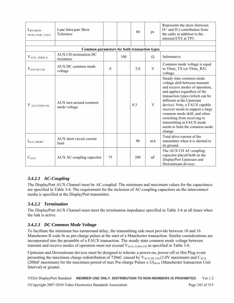
VESA DisplayPort Standard MEMBER USE ONLY. DISTRIBUTION TO NON-MEMBERS IS PROHIBITED. Ver.1.2
©Copyright 2007-2010 Video Electronics Standards Association Page 343 of 515
LRX-SKEW-
INTRA_PAIR _FAUX Lane Intra-pair Skew Tolerance 60 ps
Represents the skew (between D+ and D-) contribution from the cable in addition to the stressed EYE at TP3.
Common parameters for both transaction types
VAUX-_TERM_R AUX CH termination DC resistance 100 Ω Informative
VAUX-DC-CM AUX DC common mode voltage 0 2.0 V
Common mode voltage is equal to Vbias_TX (or Vbias_RX) voltage.
V AUX-TURN-CM AUX turn around common mode voltage 0.3 V
Steady state common mode voltage shift between transmit and receive modes of operation, and applies regardless of the transaction types (which can be different at the Upstream device). Note, a FAUX capable receiver needs to support a large common mode shift, and when switching from receiving to transmitting in FAUX mode needs to limit the common mode change
IAUX_SHORT AUX short circuit current limit 90 mA
Total drive current of the transmitter when it is shorted to its ground.
CAUX AUX AC-coupling capacitor 75 200 nF
The AUX CH AC-coupling capacitor placed both on the DisplayPort Upstream and Downstream devices
3.4.2.1 AC-Coupling The DisplayPort AUX Channel must be AC-coupled. The minimum and maximum values for the capacitance are specified in Table 3-6. The requirement for the inclusion of AC-coupling capacitors on the interconnect media is specified at the DisplayPort transmitter.
3.4.2.2 Termination The DisplayPort AUX Channel must meet the termination impedance specified in Table 3-6 at all times when the link is active.
3.4.2.3 DC Common Mode Voltage To facilitate the minimum bus turnaround delay, the transmitting side must provide between 10 and 16 Manchester-II code 0s as pre-charge pulses at the start of a Manchester transaction. Similar considerations are incorporated into the preamble of a FAUX transaction. The steady state common mode voltage between transmit and receive modes of operation must not exceed VAUX-TURN-CM as specified in Table 3-6.
Upstream and Downstream devices must be designed to tolerate a power-on, power-off or Hot Plug event presenting the maximum charge redistribution of 720nC caused by VAUX-DC-CM (2.0V maximum) and CAUX (200nF maximum) for the maximum period of max Pre-charge Pulses x UIMAN (Manchester transaction Unit Interval) or greater.
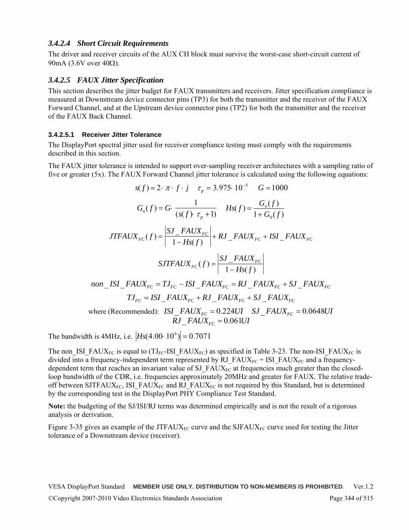
VESA DisplayPort Standard MEMBER USE ONLY. DISTRIBUTION TO NON-MEMBERS IS PROHIBITED. Ver.1.2
©Copyright 2007-2010 Video Electronics Standards Association Page 344 of 515
3.4.2.4 Short Circuit Requirements The driver and receiver circuits of the AUX CH block must survive the worst-case short-circuit current of 90mA (3.6V over 40Ω).
3.4.2.5 FAUX Jitter Specification This section describes the jitter budget for FAUX transmitters and receivers. Jitter specification compliance is measured at Downstream device connector pins (TP3) for both the transmitter and the receiver of the FAUX Forward Channel, and at the Upstream device connector pins (TP2) for both the transmitter and the receiver of the FAUX Back Channel.
3.4.2.5.1 Receiver Jitter Tolerance The DisplayPort spectral jitter used for receiver compliance testing must comply with the requirements described in this section.
The FAUX jitter tolerance is intended to support over-sampling receiver architectures with a sampling ratio of five or greater (5x). The FAUX Forward Channel jitter tolerance is calculated using the following equations:
s( f ) = 2 ⋅ π ⋅ f ⋅ j τ p = 3.975⋅ 10−5 G =1000
Go( f ) = G⋅1
(s( f )⋅ τ p +1) Hs( f ) =
Go( f )1+ G0( f )
JTFAUXFC ( f ) =SJ _ FAUXFC
1 − Hs( f )+ RJ _ FAUXFC + ISI _ FAUXFC
SJTFAUXFC ( f ) =SJ _ FAUXFC
1 − Hs( f )
non _ ISI_ FAUXFC = TJFC − ISI _ FAUXFC = RJ _ FAUXFC + SJ _ FAUXFC TJFC = ISI _ FAUXFC + RJ _ FAUXFC + SJ _ FAUXFC
where (Recommended): ISI _ FAUXFC = 0.224UI SJ _ FAUXFC = 0.0648UI RJ _ FAUXFC = 0.061UI
The bandwidth is 4MHz, i.e. Hs(4.00⋅ 106) = 0.7071
The non_ISI_FAUXFC is equal to (TJFC-ISI_FAUXFC) as specified in Table 3-23. The non-ISI_FAUXFC is divided into a frequency-independent term represented by RJ_FAUXFC + ISI_FAUXFC and a frequency-dependent term that reaches an invariant value of SJ_FAUXFC at frequencies much greater than the closed-loop bandwidth of the CDR, i.e. frequencies approximately 20MHz and greater for FAUX. The relative trade-off between SJTFAUXFC, ISI_FAUXFC and RJ_FAUXFC is not required by this Standard, but is determined by the corresponding test in the DisplayPort PHY Compliance Test Standard.
Note: the budgeting of the SJ/ISI/RJ terms was determined empirically and is not the result of a rigorous analysis or derivation.
Figure 3-35 gives an example of the JTFAUXFC curve and the SJFAUXFC curve used for testing the Jitter tolerance of a Downstream device (receiver).
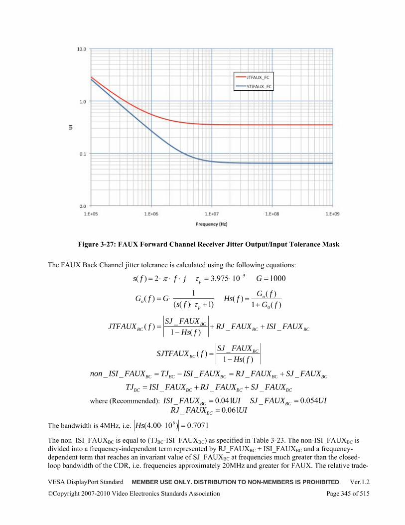
VESA DisplayPort Standard MEMBER USE ONLY. DISTRIBUTION TO NON-MEMBERS IS PROHIBITED. Ver.1.2
©Copyright 2007-2010 Video Electronics Standards Association Page 345 of 515
Figure 3-27: FAUX Forward Channel Receiver Jitter Output/Input Tolerance Mask
The FAUX Back Channel jitter tolerance is calculated using the following equations:
s( f ) = 2 ⋅ π ⋅ f ⋅ j τ p = 3.975⋅ 10−5 G =1000
Go( f ) = G⋅1
(s( f )⋅ τ p +1) Hs( f ) =
Go( f )1+ G0( f )
JTFAUXBC ( f ) =SJ _ FAUXBC
1 − Hs( f )+ RJ _ FAUXBC + ISI _ FAUXBC
SJTFAUXBC ( f ) =SJ _ FAUXBC
1 − Hs( f )
non _ ISI _ FAUXBC = TJBC − ISI _ FAUXBC = RJ _ FAUXBC + SJ _ FAUXBC
TJBC = ISI _ FAUXBC + RJ _ FAUXBC + SJ _ FAUXBC
where (Recommended): ISI _ FAUXBC = 0.041UI SJ _ FAUXBC = 0.054UI RJ _ FAUXBC = 0.061UI
The bandwidth is 4MHz, i.e. Hs(4.00⋅ 106) = 0.7071
The non_ISI_FAUXBC is equal to (TJBC-ISI_FAUXBC) as specified in Table 3-23. The non-ISI_FAUXBC is divided into a frequency-independent term represented by RJ_FAUXBC + ISI_FAUXBC and a frequency-dependent term that reaches an invariant value of SJ_FAUXBC at frequencies much greater than the closed-loop bandwidth of the CDR, i.e. frequencies approximately 20MHz and greater for FAUX. The relative trade-
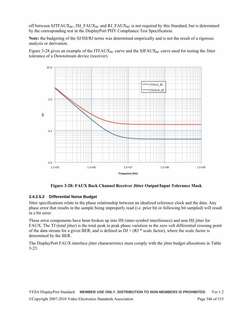
VESA DisplayPort Standard MEMBER USE ONLY. DISTRIBUTION TO NON-MEMBERS IS PROHIBITED. Ver.1.2
©Copyright 2007-2010 Video Electronics Standards Association Page 346 of 515
off between SJTFAUXBC, ISI_FAUXBC and RJ_FAUXBC is not required by this Standard, but is determined by the corresponding test in the DisplayPort PHY Compliance Test Specification.
Note: the budgeting of the SJ/ISI/RJ terms was determined empirically and is not the result of a rigorous analysis or derivation.
Figure 3-28 gives an example of the JTFAUXBC curve and the SJFAUXBC curve used for testing the Jitter tolerance of a Downstream device (receiver).
Figure 3-28: FAUX Back Channel Receiver Jitter Output/Input Tolerance Mask
3.4.2.5.2 Differential Noise Budget Jitter specifications relate to the phase relationship between an idealized reference clock and the data. Any phase error that results in the sample being improperly read (i.e. prior bit or following bit sampled) will result in a bit error.
These error components have been broken up into ISI (inter-symbol interference) and non-ISI jitter for FAUX. The TJ (total jitter) is the total peak to peak phase variation in the zero volt differential crossing point of the data stream for a given BER, and is defined as DJ + (RJ * scale factor), where the scale factor is determined by the BER.
The DisplayPort FAUX interface jitter characteristics must comply with the jitter budget allocations in Table 3-23.
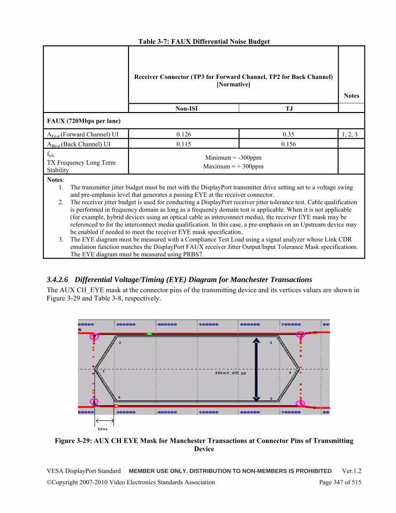
VESA DisplayPort Standard MEMBER USE ONLY. DISTRIBUTION TO NON-MEMBERS IS PROHIBITED. Ver.1.2
©Copyright 2007-2010 Video Electronics Standards Association Page 347 of 515
Table 3-7: FAUX Differential Noise Budget
Receiver Connector (TP3 for Forward Channel, TP2 for Back Channel) [Normative]
Notes
Non-ISI TJ
FAUX (720Mbps per lane)
AFp-p (Forward Channel) UI 0.126 0.35 1, 2, 3 ABp-p (Back Channel) UI 0.115 0.156 ftol,
TX Frequency Long Term Stability
Minimum = -300ppm Maximum = + 300ppm
Notes: 1. The transmitter jitter budget must be met with the DisplayPort transmitter drive setting set to a voltage swing
and pre-emphasis level that generates a passing EYE at the receiver connector. 2. The receiver jitter budget is used for conducting a DisplayPort receiver jitter tolerance test. Cable qualification
is performed in frequency domain as long as a frequency domain test is applicable. When it is not applicable (for example, hybrid devices using an optical cable as interconnect media), the receiver EYE mask may be referenced to for the interconnect media qualification. In this case, a pre-emphasis on an Upstream device may be enabled if needed to meet the receiver EYE mask specification.
3. The EYE diagram must be measured with a Compliance Test Load using a signal analyzer whose Link CDR emulation function matches the DisplayPort FAUX receiver Jitter Output/Input Tolerance Mask specifications. The EYE diagram must be measured using PRBS7.
3.4.2.6 Differential Voltage/Timing (EYE) Diagram for Manchester Transactions The AUX CH_EYE mask at the connector pins of the transmitting device and its vertices values are shown in Figure 3-29 and Table 3-8, respectively.
1
2 3
4
56
390mV_diff_pp
50ns Figure 3-29: AUX CH EYE Mask for Manchester Transactions at Connector Pins of Transmitting
Device
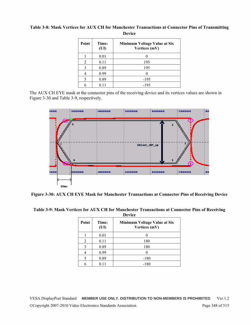
VESA DisplayPort Standard MEMBER USE ONLY. DISTRIBUTION TO NON-MEMBERS IS PROHIBITED. Ver.1.2
©Copyright 2007-2010 Video Electronics Standards Association Page 348 of 515
Table 3-8: Mask Vertices for AUX CH for Manchester Transactions at Connector Pins of Transmitting Device
Point Time: (UI)
Minimum Voltage Value at Six Vertices (mV)
1 0.01 0 2 0.11 195 3 0.89 195 4 0.99 0 5 0.89 -195 6 0.11 -195
The AUX CH EYE mask at the connector pins of the receiving device and its vertices values are shown in Figure 3-30 and Table 3-9, respectively.
Figure 3-30: AUX CH EYE Mask for Manchester Transactions at Connector Pins of Receiving Device
Table 3-9: Mask Vertices for AUX CH for Manchester Transactions at Connector Pins of Receiving Device
Point Time: (UI)
Minimum Voltage Value at Six Vertices (mV)
1 0.01 0 2 0.11 180 3 0.89 180 4 0.99 0 5 0.89 -180 6 0.11 -180
VESA DisplayPort Standard MEMBER USE ONLY. DISTRIBUTION TO NON-MEMBERS IS PROHIBITED. Ver.1.2
©Copyright 2007-2010 Video Electronics Standards Association Page 349 of 515
3.4.2.7 Differential Voltage/timing (EYE) Diagram for FAUX Transactions The EYE diagram is used to measure compliance of the Forward Channel transmitter and the Back Channel receiver for Upstream devices and the Back Channel transmitter and the Forward Channel receiver for Downstream devices.
FAUX uses a pre-defined polygon for the EYE diagram. The polygon in Figure 3-31 represents the FAUX transmitter EYE Mask for the Forward Channel transmitter taken after a reference cable at TP3 and for the Back Channel transmitter taken after a reference cable at TP2. For Downstream devices with a permanently attached cable, a reference extension cable is used during compliance testing in conjunction with the TP2 transmitter mask.
Table 3-25 contains the values to be used for the vertices of the mask for FAUX Forward Channel transmitter, and Table 3-11 contains the values to be used for the vertices of the mask for the FAUX Back Channel transmitter. The FAUX Back Channel from a Downstream device with a permanently attached cable has the same transmit EYE mask at TP2 as the Back Channel from a Downstream device with a receptacle. The EYE diagram must be measured at TP3 (for the Forward Channel) or at TP2 (for the Back Channel) with a Compliance Test Load using a signal analyzer whose Link CDR emulation function meets the requirements specified in Section 3.5.3.5 and matches the DisplayPort receiver Jitter Output/Input Tolerance Mask specifications in Section 3.4.2.5.1 within +/-10% of accuracy.
The measured EYE must be equal to or larger than the EYE Mask. The transmitted pattern must be PRBS7. At least one combination of differential voltage swing and pre-emphasis must result in an EYE that meets the appropriate (Forward Channel or Back Channel) EYE mask specification.
For the FAUX Forward Channel no specific combination of voltage swing and pre-emphasis is required to generate a passing EYE. It is recommended that a passing EYE be generated at least one of voltage swing level 1/pre-emphasis level 2, voltage swing level 2/pre-emphasis levels 0 or 1, or voltage swing level 3/pre-emphasis level 0. Voltage swing level 2/pre-emphasis level 1 may be found to be the most appropriate for typical Upstream devices
For the FAUX Back Channel no specific combination of voltage swing and pre-emphasis is required to generate a passing EYE. It is recommended that a passing EYE be generated at least one of voltage swing level 1/pre-emphasis level 2, voltage swing level 2/pre-emphasis levels 0 or 1, or voltage swing level 3/pre-emphasis level 0. Voltage swing level 1/pre-emphasis level 2 may be found to be the most appropriate for typical Downstream devices
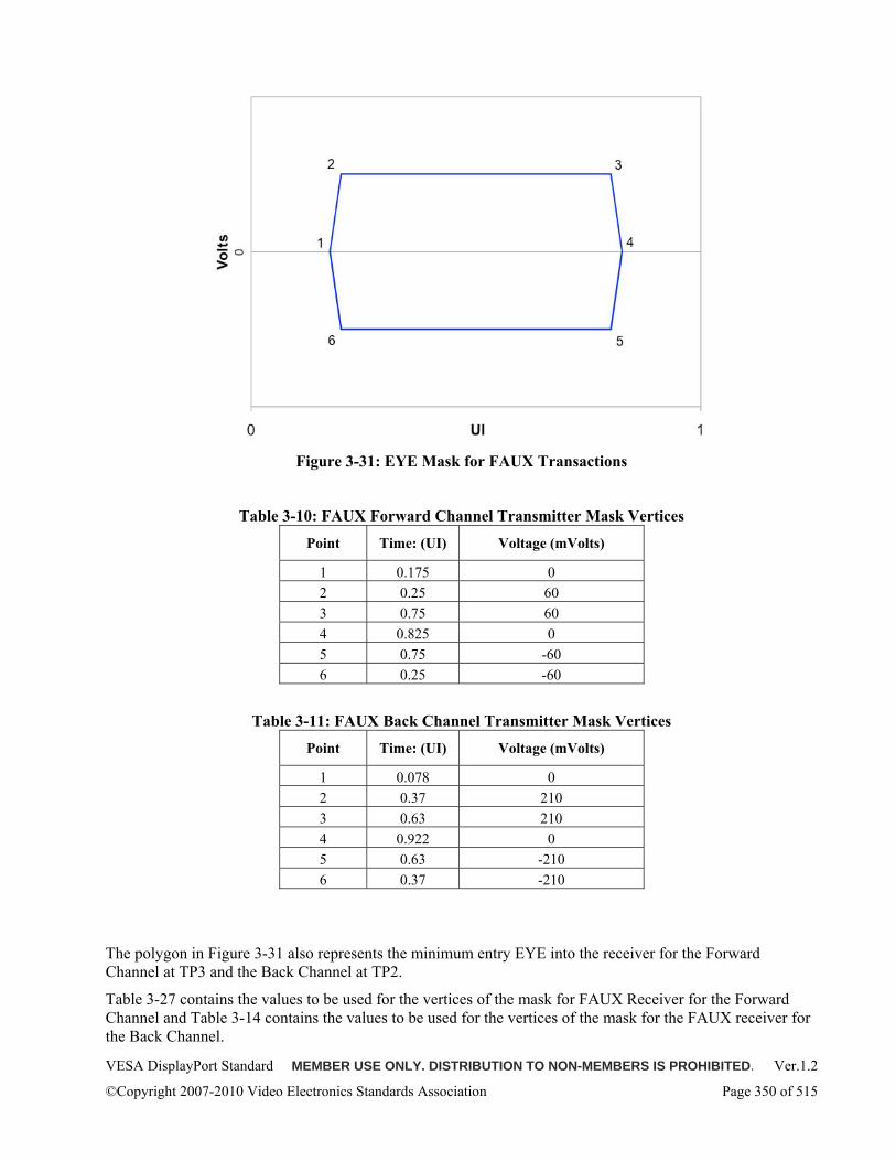
VESA DisplayPort Standard MEMBER USE ONLY. DISTRIBUTION TO NON-MEMBERS IS PROHIBITED. Ver.1.2
©Copyright 2007-2010 Video Electronics Standards Association Page 350 of 515
Figure 3-31: EYE Mask for FAUX Transactions
Table 3-10: FAUX Forward Channel Transmitter Mask Vertices
Point Time: (UI) Voltage (mVolts)
1 0.175 0 2 0.25 60 3 0.75 60 4 0.825 0 5 0.75 -60 6 0.25 -60
Table 3-11: FAUX Back Channel Transmitter Mask Vertices
Point Time: (UI) Voltage (mVolts)
1 0.078 0 2 0.37 210 3 0.63 210 4 0.922 0 5 0.63 -210 6 0.37 -210
The polygon in Figure 3-31 also represents the minimum entry EYE into the receiver for the Forward Channel at TP3 and the Back Channel at TP2.
Table 3-27 contains the values to be used for the vertices of the mask for FAUX Receiver for the Forward Channel and Table 3-14 contains the values to be used for the vertices of the mask for the FAUX receiver for the Back Channel.
VESA DisplayPort Standard MEMBER USE ONLY. DISTRIBUTION TO NON-MEMBERS IS PROHIBITED. Ver.1.2
©Copyright 2007-2010 Video Electronics Standards Association Page 351 of 515
To test a Forward Channel receiver on a device with a permanently attached cable, the transmitter EYE mask defined at TP2, specified in Table 3-25, is used in conjunction with either an extension cable model (if the device has a Mini DisplayPort connector) or an adaptor cable model (if the device has a full-size DisplayPort connector).
This EYE Mask is used for testing the jitter tolerance of FAUX Receiver Device. A test pattern generator, while transmitting the PRBS7 bit stream must be adjusted to realize the minimum EYE. The rise / fall time must be set to 130ps for 20-80% transition.
Once the test pattern generator is adjusted, the PRBS7 bit stream must be sent to the connector pins (TP2 or TP3 as appropriate) of the FAUX Receiver Device. With this input, the Receiver must realize a BER of 1E-12 or better.
Table 3-12: FAUX Forward Channel Receiver EYE Vertices
Point Time: (UI) Voltage (mVolts)
1 0.175 0 2 0.25 60 3 0.75 60 4 0.825 0 5 0.75 -60 6 0.25 -60
Table 3-13: Table 3-14: FAUX Back Channel Receiver EYE Vertices
Point Time: (UI) Voltage (mVolts)
1 0.078 0 2 0.37 210 3 0.63 210 4 0.922 0 5 0.63 -210 6 0.37 -210
3.4.2.8 FAUX Test Modes For EYE diagram measurements, a special test mode is defined. In this mode the reference receiver (either a DisplayPlayPort Upstream device or a DisplayPort Downstream device) is able to command the device under test (a DisplayPort Downstream device or a DisplayPort Upstream device) to send a test pattern for 30 seconds. At the end of transmitting the test pattern, normal AUX operation resumes (using either FAUX transactions or Manchester transactions). Crosstalk testing of the AUX channel to the main link shall must place with the main link with spread spectrum turned on except for Upstream devices that do not support spread spectrum. Crosstalk testing will be performed by running the main link and running busy FAUX traffic (repeated DPCD reads and writes of variable length up to the maximum with no delays between them).
The test patterns for the test packets are scrambled then 8B10B encoded zeros, unscrambled D10.2 symbols, and PRBS7. The test packets are framed as normal FAUX packets (with pre-amble, packet start K code and packet end K code) but with packet length as necessary for a 30 second duration.
3.4.2.9 FAUX Error Count Registers Both the Upstream device and the Downstream device must maintain error count registers. The FAUX receiver must ignore any errors it detects during the Preamble. The error counter must be enabled (but not
VESA DisplayPort Standard MEMBER USE ONLY. DISTRIBUTION TO NON-MEMBERS IS PROHIBITED. Ver.1.2
©Copyright 2007-2010 Video Electronics Standards Association Page 352 of 515
cleared) when the receiver receives FAUX_START or XUSB_FRAME_START and disabled when the receiver receives FAUX_END or XUSB_FRAME_END. The number of illegal symbols or disparity errors are controlled by the SYMBOL ERROR COUNT SEL field of TRAINING_PATTERN_SET (DPCD 00102h)
The Downstream device must maintain its error count in FAUX_FORWARD_CHANNEL_SYMBOL_ERROR_COUNT. The number of illegal symbols or disparity errors are controlled by the FAUX_FORWARD_CHANNEL_SYMBOL ERROR COUNT SEL field of FAUX_MODE_CTRL (DPCD 00120h).
The Upstream device must maintain an internal error counter. The number of illegal symbols or disparity errors are controlled by the FAUX_BACK_CHANNEL_SYMBOL ERROR COUNT SEL field of FAUX_BACK_CHANNEL_SYMBOL ERROR COUNT_CONTROL (DPCD 00282h) The Upstream device must write its error count to the FAUX_BACK_CHANNEL_SYMBOL_ERROR_COUNT register whenever commanded by the Downstream device device setting FAUX_BACK_CHANNEL_ERROR_COUNT REQUEST in DPCD register 00249h and asserting HPD_IRQ.
3.4.2.10 FAUX Power Control The SET_PWR DPCD control at DPCD register 600h supports the operation of the AUX channel simultaneously with placing the main link into a low power state (Main Link Only Power Down Mode). In this power state, the Downstream device powers down the main link receivers and keeps its AUX block in normal state, ready. If FAUX is supported, and FAUX_EN is set, it keeps its FAUX block active, ready to reply within a Response Time-Out period 0.6μs to FAUX transactions (FAUX Power State 1) or with Squelch detection enabled ready to bring its FAUX circuitry back to full power within 2μs (FAUX Power State 2), and ready to reply within a Response Time-Out period of 300μs to Manchester transactions. If FAUX is not supported, or if FAUX_EN is not set, then Main Link Only Power Down Mode (DPCD 00600h set to 0b101) is treated identically to Power Down Mode (DPCD 00600h set to 0b001).
When FAUX_EN is set, the Downstream device must check the current value of DPCD 00600h and set the appropriate power states.
Note that it is valid for the Upstream device to power down and power up the FAUX capabilities during Main Link Only Power Down Mode) by clearing and setting FAUX_EN. For example it is valid for the Upstream device to set DPCD 00600h to 0b101, and to clear FAUX_EN (following which the Main Link and FAUX and Manchester circuits may all be powered down), then to perform Manchester transaction writes to FAUX_EN (repeating these until the AUX line wakes up and the transaction is acknowledged) without writing to DPCD 00600h (leaving it at 0b101) in order to transition to the state in which the main link is powered down but FAUX is active.
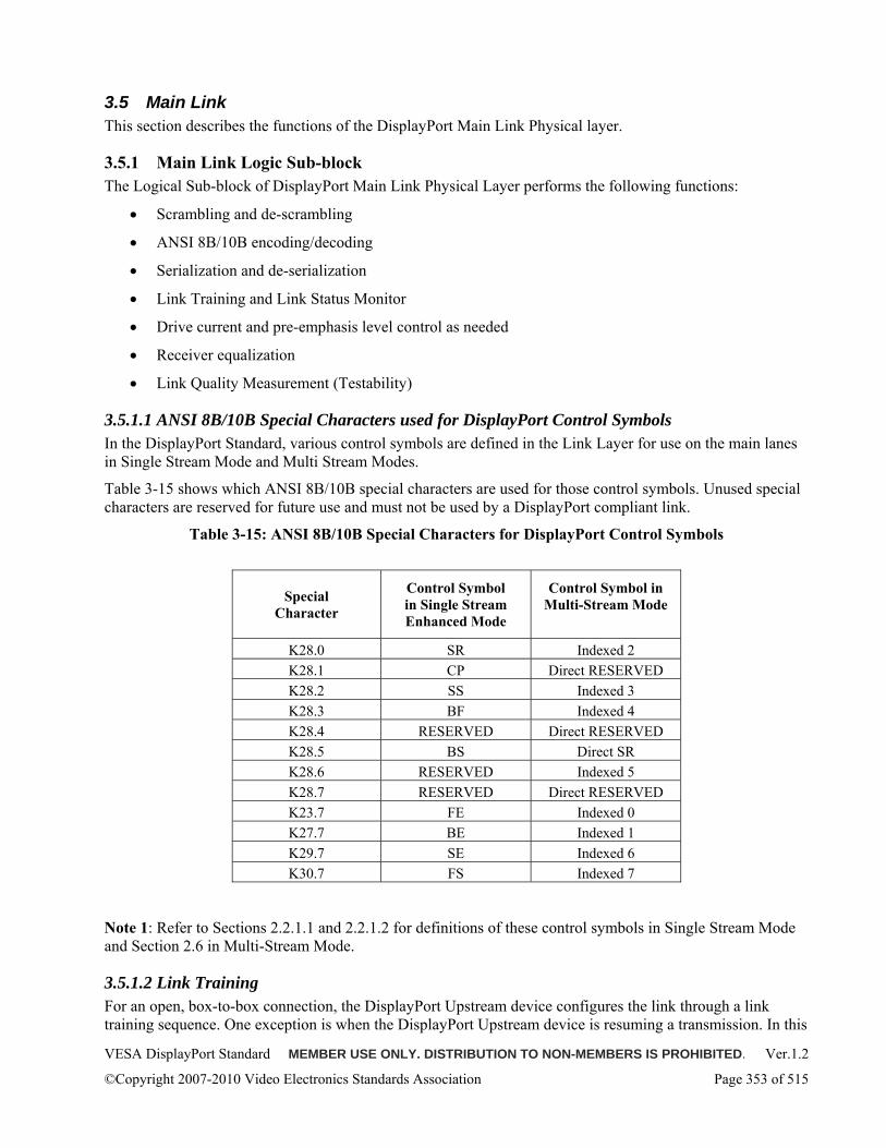
VESA DisplayPort Standard MEMBER USE ONLY. DISTRIBUTION TO NON-MEMBERS IS PROHIBITED. Ver.1.2
©Copyright 2007-2010 Video Electronics Standards Association Page 353 of 515
3.5 Main Link This section describes the functions of the DisplayPort Main Link Physical layer.
3.5.1 Main Link Logic Sub-block The Logical Sub-block of DisplayPort Main Link Physical Layer performs the following functions:
• Scrambling and de-scrambling
• ANSI 8B/10B encoding/decoding
• Serialization and de-serialization
• Link Training and Link Status Monitor
• Drive current and pre-emphasis level control as needed
• Receiver equalization
• Link Quality Measurement (Testability)
3.5.1.1 ANSI 8B/10B Special Characters used for DisplayPort Control Symbols In the DisplayPort Standard, various control symbols are defined in the Link Layer for use on the main lanes in Single Stream Mode and Multi Stream Modes.
Table 3-15 shows which ANSI 8B/10B special characters are used for those control symbols. Unused special characters are reserved for future use and must not be used by a DisplayPort compliant link.
Table 3-15: ANSI 8B/10B Special Characters for DisplayPort Control Symbols
Special Character
Control Symbol in Single Stream Enhanced Mode
Control Symbol in Multi-Stream Mode
K28.0 SR Indexed 2 K28.1 CP Direct RESERVED K28.2 SS Indexed 3 K28.3 BF Indexed 4 K28.4 RESERVED Direct RESERVED K28.5 BS Direct SR K28.6 RESERVED Indexed 5 K28.7 RESERVED Direct RESERVED K23.7 FE Indexed 0 K27.7 BE Indexed 1 K29.7 SE Indexed 6 K30.7 FS Indexed 7
Note 1: Refer to Sections 2.2.1.1 and 2.2.1.2 for definitions of these control symbols in Single Stream Mode and Section 2.6 in Multi-Stream Mode.
3.5.1.2 Link Training For an open, box-to-box connection, the DisplayPort Upstream device configures the link through a link training sequence. One exception is when the DisplayPort Upstream device is resuming a transmission. In this
VESA DisplayPort Standard MEMBER USE ONLY. DISTRIBUTION TO NON-MEMBERS IS PROHIBITED. Ver.1.2
©Copyright 2007-2010 Video Electronics Standards Association Page 354 of 515
condition, the Upstream device may skip the AUX CH handshake for the link training as described in Section 2.9.3.4.
For a closed embedded connection, the DisplayPort transmitter and receiver may be set to pre-calibrated parameters without going through the full link training sequence. In this mode, the DisplayPort Upstream device may start a normal operation without the AUX CH handshake for link training, as described in Section 2.9.3.4.
Main Link training will normally take place after FAUX training (where both devices support FAUX). Manchester AUX transactions must be used for the DPCD reads and writes directly related to the training process during main link training. A DisplayPort receiver must support main link training using Manchester transactions.
During main link training when both the Upstream device and the Downstream device are FAUX capable, the Upstream device must, whenever it is not engaged in AUX transactions directly associated with training, continuously perform maximum length (16 byte) reads from the Downstream device DPCD registers using FAUX transactions. This is to ensure that any signal degradation due to crosstalk at the Downstream device between the FAUX transmitter and the main link receiver is compensated for during main link training.
Link training consists of two distinct tasks which must be completed successfully in sequence to establish the link. These are:
• Clock Recovery: This stage locks the receiver CR (clock recovery) PLL to the repetition of D10.2 data symbols.
• Channel Equalization / Symbol-Lock / Inter-lane Alignment: When successful, the Symbol-Lock and Inter-lane alignment must be achieved by the end of this sequence.
The training sequence is initiated by the Link Policy Maker in the Upstream device after detecting an HPD event. When the Upstream device detects an HPD low-going pulse that exceeds 2ms in width, the Link Policy Maker must read the link capability field of the DPCD via the AUX CH. The Link Policy Maker must then, determine the link configuration based on the capability of DisplayPort Receiver and its own needs, write the Link Configuration parameters (LINK_BW_SET, LANE_COUNT_SET, DOWNSPREAD_CTRL, MAIN_LINK_CHANNEL_CODING_SET) to the link configuration field of DPCD, and then start the Link Training by writing 21h to the TRAINING_PATTERN_SET byte of the DPCD (DisplayPort Configuration Data) of the DisplayPort receiver at Address 102h via the AUX CH while instructing its transmitter PHY logic sub-layer to start transmitting training patterns.
The Link Configuration parameters LINK_BW_SET, LANE_COUNT_SET, DOWNSPREAD_CTRL and MAIN_LINK_CHANNEL_CODING_SET must not be changed after training has commenced until the next time the link is trained except as described below for falling back to lower bandwidth on training failure.
Writing 21h to TRAINING_PATTERN_SET byte at Address 102h via AUX CH by a DisplayPort Upstream device must be preceded by the change of transmitted training pattern over Main Link. Whenever Address 102h is written to, the TRAINING_LANEx_SET bytes (Addresses 103h ~ 106h) of the enabled lanes must be written. Note that the number of enabled lanes is written to LANE_COUNT_SET at Address 101h prior to Link Training. The AUX CH burst write must be used for writing to TRAINING_LANEx_SET bytes of the enabled lanes. An Upstream device may write to TRAINING_PATTERN_SET and TRAINING_LANEx_SET bytes in one AUX CH burst write transaction.
A per-lane drive setting adjustability is an optional feature of a DisplayPort transmitter. If a DisplayPort receiver requests different drive settings among multiple (2 or 4) lanes, a DisplayPort transmitter may use the setting of highest pre-emphasis level and voltage swing of all the requested settings.
When the combination of the requested pre-emphasis level and voltage swing exceeds the capability of a DisplayPort transmitter, the transmitter must set the pre-emphasis level according to the request and use the highest voltage swing it can output with the given pre-emphasis level.
VESA DisplayPort Standard MEMBER USE ONLY. DISTRIBUTION TO NON-MEMBERS IS PROHIBITED. Ver.1.2
©Copyright 2007-2010 Video Electronics Standards Association Page 355 of 515
A DisplayPort receiver must issue a drive setting adjustment request within limits defined in this Standard.
When a DisplayPort transmitter reads a request outside the DisplayPort Standard limit, the transmitter must set the pre-emphasis level according to the request and set the highest voltage swing level it can output with the given pre-emphasis level. If a DisplayPort transmitter is requested for 9.5dB of pre-emphasis level (the support of which is optional for a transmitter) and cannot support that level, it must set the pre-emphasis level to the next highest level, 6dB.
A DisplayPort transmitter may support Post Cursor2 at any combination of bit rates. If it supports Post Cursor2 at the bit rate at which the link is being trained, then it must inspect the ADJUST_REQUEST_POST_CURSOR2 DPCD registers whenever it inspects the ADJUST_REQUEST_LANEx_y DPCD registers, must adjust the Post Cursor2 setting of the transmitted signal accordingly, and must notify the DisplayPort receiver by setting the TRAINING_LANEx_y_SET2 registers. The receiver can determine that the transmitter does not support Post Cursor2 at the bit rate at which the link is being trained either by observing that the TRAINING_LANEx_y_SET2 registers are not written to, or by observing that Lanex MAX_POST CURSOR2_REACHED is set at Post Cursor2 Level 0.
The Link Policy Maker of the Upstream device may choose any link count and link rate as long as they do not exceed the capabilities of the DisplayPort Receiver. Link Training starts when the DisplayPort transmitter writes the link configuration and sets the Link Training Pattern to the Link Configuration Field of the DPCD. Link training is expected to complete within 10ms. Table 3-16 shows the link training symbol patterns. All devices must support TPS1 and TPS2. An HBR2 capable device must also support TPS3. A device not capable of HBR2 is recommended to support TPS3. A Downstream device that is capable of supporting TPS3 must advertise this capability by setting the TPS3_SUPPORTED capability bit in DPCD 00002h. An Upstream device that supports TPS3 must inspect the TPS3_SUPPORTED bit in the attached Downstream device, and if it finds this bit is set, must transmit TPS3 during the Channel Equalization phase of link training (regardless of the speed at which the link is being trained). In all other cases, the Upstream device must transmit TPS2 during the Channel Equalization phase of link training If training without AUX CH handshake, then the use of TPS3 is determined either as the result of a previous training phase on the same connection, or by implementation-dependent system configuration means (for example, on eDP).
Unless training without AUX CH handshake, a DisplayPort receiver may request for adjustment of differential voltage swing, pre-emphasis, or both during the Clock Recovery phase and the Channel Equalization phase of Link Training procedure as shown in Figure 3-32 and Figure 3-33.
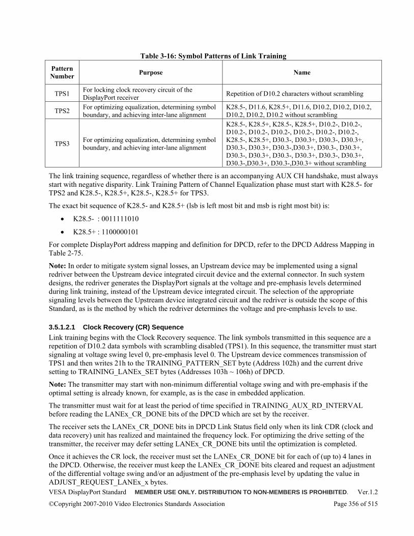
VESA DisplayPort Standard MEMBER USE ONLY. DISTRIBUTION TO NON-MEMBERS IS PROHIBITED. Ver.1.2
©Copyright 2007-2010 Video Electronics Standards Association Page 356 of 515
Table 3-16: Symbol Patterns of Link Training
Pattern Number Purpose Name
TPS1 For locking clock recovery circuit of the DisplayPort receiver Repetition of D10.2 characters without scrambling
TPS2 For optimizing equalization, determining symbol boundary, and achieving inter-lane alignment
K28.5-, D11.6, K28.5+, D11.6, D10.2, D10.2, D10.2, D10.2, D10.2, D10.2 without scrambling
TPS3 For optimizing equalization, determining symbol boundary, and achieving inter-lane alignment
K28.5-, K28.5+, K28.5-, K28.5+, D10.2-, D10.2-, D10.2-, D10.2-, D10.2-, D10.2-, D10.2-, D10.2-, K28.5-, K28.5+, D30.3-, D30.3+, D30.3-, D30.3+, D30.3-, D30.3+, D30.3-,D30.3+, D30.3-, D30.3+, D30.3-, D30.3+, D30.3-, D30.3+, D30.3-, D30.3+, D30.3-,D30.3+, D30.3-,D30.3+ without scrambling
The link training sequence, regardless of whether there is an accompanying AUX CH handshake, must always start with negative disparity. Link Training Pattern of Channel Equalization phase must start with K28.5- for TPS2 and K28.5-, K28.5+, K28.5-, K28.5+ for TPS3.
The exact bit sequence of K28.5- and K28.5+ (lsb is left most bit and msb is right most bit) is:
• K28.5- : 0011111010
• K28.5+ : 1100000101
For complete DisplayPort address mapping and definition for DPCD, refer to the DPCD Address Mapping in Table 2-75.
Note: In order to mitigate system signal losses, an Upstream device may be implemented using a signal redriver between the Upstream device integrated circuit device and the external connector. In such system designs, the redriver generates the DisplayPort signals at the voltage and pre-emphasis levels determined during link training, instead of the Upstream device integrated circuit. The selection of the appropriate signaling levels between the Upstream device integrated circuit and the redriver is outside the scope of this Standard, as is the method by which the redriver determines the voltage and pre-emphasis levels to use.
3.5.1.2.1 Clock Recovery (CR) Sequence Link training begins with the Clock Recovery sequence. The link symbols transmitted in this sequence are a repetition of D10.2 data symbols with scrambling disabled (TPS1). In this sequence, the transmitter must start signaling at voltage swing level 0, pre-emphasis level 0. The Upstream device commences transmission of TPS1 and then writes 21h to the TRAINING_PATTERN_SET byte (Address 102h) and the current drive setting to TRAINING_LANEx_SET bytes (Addresses 103h ~ 106h) of DPCD.
Note: The transmitter may start with non-minimum differential voltage swing and with pre-emphasis if the optimal setting is already known, for example, as is the case in embedded application.
The transmitter must wait for at least the period of time specified in TRAINING_AUX_RD_INTERVAL before reading the LANEx_CR_DONE bits of the DPCD which are set by the receiver.
The receiver sets the LANEx_CR_DONE bits in DPCD Link Status field only when its link CDR (clock and data recovery) unit has realized and maintained the frequency lock. For optimizing the drive setting of the transmitter, the receiver may defer setting LANEx_CR_DONE bits until the optimization is completed.
Once it achieves the CR lock, the receiver must set the LANEx_CR_DONE bit for each of (up to) 4 lanes in the DPCD. Otherwise, the receiver must keep the LANEx_CR_DONE bits cleared and request an adjustment of the differential voltage swing and/or an adjustment of the pre-emphasis level by updating the value in ADJUST_REQUEST_LANEx_x bytes.
VESA DisplayPort Standard MEMBER USE ONLY. DISTRIBUTION TO NON-MEMBERS IS PROHIBITED. Ver.1.2
©Copyright 2007-2010 Video Electronics Standards Association Page 357 of 515
If the receiver keeps the same value in ADJUST_REQUEST_LANEx_x bytes while LANEx_CR_DONE bits remain unset, the transmitter must loop four times with the same voltage swing. On the 5th time, the transmitter must down-shift to the lower bit rate and must repeat the CR-lock training sequence as described below.
Unless all the LANEx_CR_DONE bits are set, the transmitter must read the ADJUST_REQUEST_LANEx_x, increase the voltage swing and/or pre-emphasis level according to the request, and update the TRAINING_LANEx_SET bytes to match the new voltage swing and/or pre-emphasis settings.
Section 3.1.5.2 gives the voltage swings that the transmitter must support.
If the maximum available differential voltage swing fails to realize the CR lock, the transmitter must down-shift to a lower bit rate (as indicated to the receiver by an AUX CH write to the LINK_BW_SET byte of the DPCD), and repeat the bit-lock training sequence. In order to re-initiate training at a lower bit rate, the Upstream device clears TRAINING_PATTERN_SET (DPCD 00102h), starts transmitting TPS1 (D10.2) at the lower rate at the default voltage swing and pre-emphasis (400mV, no pre-emphasis), then writes 21h to TRAINING_PATTERN_SET (and appropriate values to TRAINING_LANEx_SET) to initiate training.
Once it reads LANEx_CR_DONE bits set for all lanes, the Link Policy Maker of the transmitter must move on to the next stage, namely, Channel Equalization.
If any of the LANEx_CR_DONE remains unset even at the reduced bit rate after all the voltage swing values have been tried, the transmitter must end the training (by clearing the TRAINING_PATTERN_SET byte to 00h in the DPCD) without establishing the link, or, if training over two or four lanes, may attempt training on a reduced number of lanes.
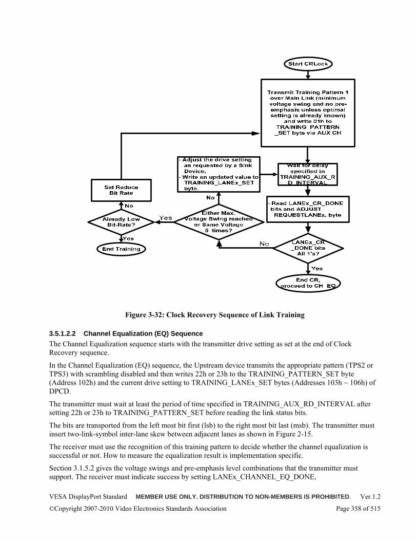
VESA DisplayPort Standard MEMBER USE ONLY. DISTRIBUTION TO NON-MEMBERS IS PROHIBITED. Ver.1.2
©Copyright 2007-2010 Video Electronics Standards Association Page 358 of 515
Figure 3-32: Clock Recovery Sequence of Link Training
3.5.1.2.2 Channel Equalization (EQ) Sequence The Channel Equalization sequence starts with the transmitter drive setting as set at the end of Clock Recovery sequence.
In the Channel Equalization (EQ) sequence, the Upstream device transmits the appropriate pattern (TPS2 or TPS3) with scrambling disabled and then writes 22h or 23h to the TRAINING_PATTERN_SET byte (Address 102h) and the current drive setting to TRAINING_LANEx_SET bytes (Addresses 103h ~ 106h) of DPCD.
The transmitter must wait at least the period of time specified in TRAINING_AUX_RD_INTERVAL after setting 22h or 23h to TRAINING_PATTERN_SET before reading the link status bits.
The bits are transported from the left most bit first (lsb) to the right most bit last (msb). The transmitter must insert two-link-symbol inter-lane skew between adjacent lanes as shown in Figure 2-15.
The receiver must use the recognition of this training pattern to decide whether the channel equalization is successful or not. How to measure the equalization result is implementation specific.
Section 3.1.5.2 gives the voltage swings and pre-emphasis level combinations that the transmitter must support. The receiver must indicate success by setting LANEx_CHANNEL_EQ_DONE,
VESA DisplayPort Standard MEMBER USE ONLY. DISTRIBUTION TO NON-MEMBERS IS PROHIBITED. Ver.1.2
©Copyright 2007-2010 Video Electronics Standards Association Page 359 of 515
LANEx_SYMBOL_LOCKED, and INTERLANE_ALIGN_DONE bits in the LANEx_x_STATUS / LANE_ALIGNED_STATUS_UPDATED bytes.
The receiver sets the LANEx_SYMBOL_LOCKED bits in DPCD Link Status field only when it has properly detected and aligned the ANSI8B/10B symbol boundaries. Given the bit error rate target of 1E-9 and the duration of the link training period (10ms or less), the receiver should detect no more than a single symbol error during the link training to set the LANEx_SYMBOL_LOCKED bits. For optimizing the drive setting of the DisplayPort transmitter, the receiver may defer setting SYMBOL_LOCK_DONE bits until the optimization is completed.
The receiver sets the INTERLANE_ALIGN_DONE bit in DPCD Link Status field only when its PHY digital sub-block has successfully aligned the symbol boundaries of all the enabled lanes with one another so that the Link Layer block can handle the incoming symbol patterns. For optimizing the drive setting of the DisplayPort transmitter, the receiver may defer setting INTERLANE_ALIGN_DONE bit until the optimization is completed.
During the normal operation following the link training, the receiver must clear the LANEx_SYMBOL_LOCKED bits and the INTERLANE_ALIGN_DONE bit when its Link Layer block can no longer process the incoming symbol patterns due to symbol errors, and thus causing noticeable visible/audible glitches to the regenerated streams. The receiver must otherwise maintain these bits during normal operation. The receiver must not clear these bits upon isolated symbol errors. Guidelines for symbol-error resiliency of the receiver are given in Appendix C.
The transmitter must read those bytes in the paragraph above and ADJUST_REQUEST_LANEx_x bytes. Unless all status bits are 1, the transmitter must then adjust the drive setting according to the request by the receiver, and write the new setting to TRAINING_LANEx_SET bytes.
The minimum loop count in this sequence is 1, while the maximum loop count in this sequence (refer to Figure 3-33) is 5. When not training at RBR and any one or more of the LANEx_SYMBOL_LOCKED and INTERLANE_ALIGN_ DONE status bits remain unset in the 6th loop, the transmitter must down-shift to the next lower bit rate. In order to re-initiate training at a lower bit rate, the Upstream device clears TRAINING_PATTERN_SET (DPCD 00102h), starts transmitting TPS1 (D10.2) at the lower rate at the default voltage swing and pre-emphasis (400mV, no pre-emphasis), then writes 21h to TRAINING_PATTERN_SET (and appropriate values to TRAINING_LANEx_SET) to initiate training.
At the end of the successful EQ sequence (with all of LANEx_SYMBOL_LOCKED and INTERLANE_ALIGN_DONE bits set by the receiver), the transmitter must clear TRAINING_PATTERN _SET byte (Address 102h) to 00h.
The receiver with its own equalizer (optional) may adjust its equalizer setting(s) in each of the training loop. The receiver may optionally issue up to seven consecutive AUX DEFERs if needed. However, it is strongly recommended that that usage of AUX DEFER be minimized to meet the Link Training completion time target of 10ms. When the transmitter receives more than seven consecutive AUX DEFERs, it may terminate the Link Training.
It is recommended that the receiver not set LANEx_CHANNEL_EQ_DONE, LANEx_SYMBOL_LOCKED, and INTERLANE_ALIGN_DONE bits right after the successful reception of training patterns. Rather, the receiver should either increase its own equalization level or request a stronger pre-emphasis. When such action results in loss of successful reception, the receiver must restore or request the last setting. The purpose of this methodology is to ensure the maximum operating margin.
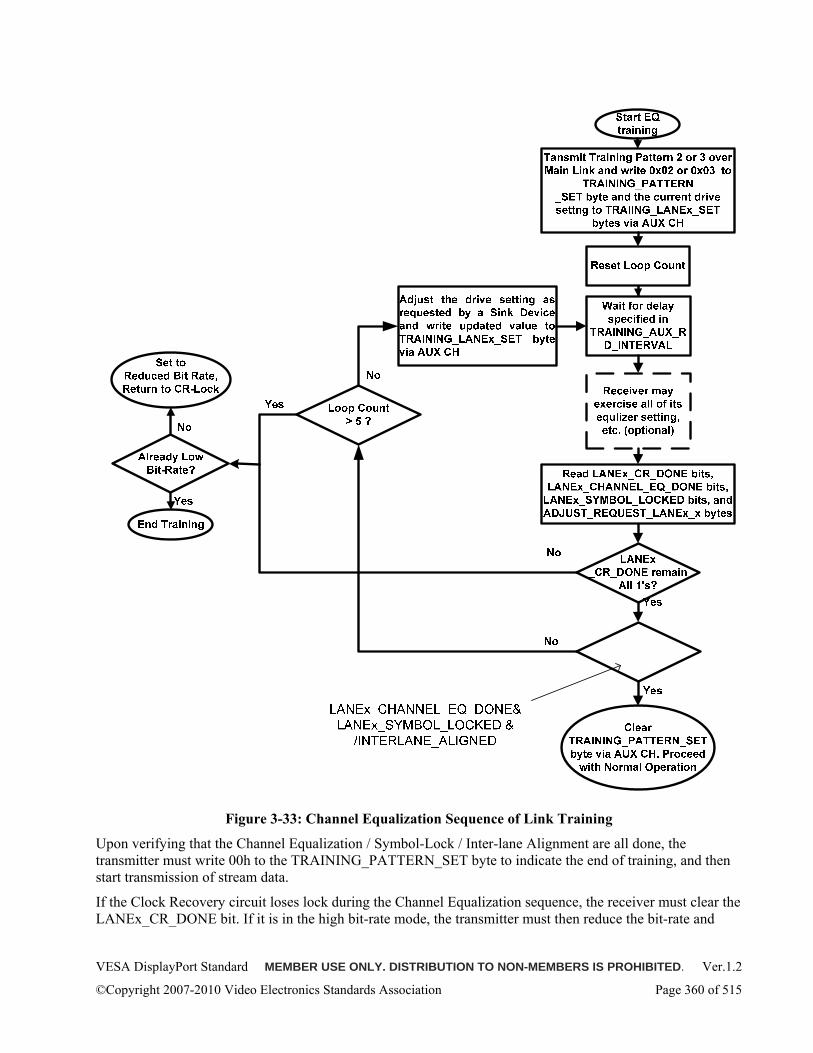
VESA DisplayPort Standard MEMBER USE ONLY. DISTRIBUTION TO NON-MEMBERS IS PROHIBITED. Ver.1.2
©Copyright 2007-2010 Video Electronics Standards Association Page 360 of 515
Figure 3-33: Channel Equalization Sequence of Link Training
Upon verifying that the Channel Equalization / Symbol-Lock / Inter-lane Alignment are all done, the transmitter must write 00h to the TRAINING_PATTERN_SET byte to indicate the end of training, and then start transmission of stream data.
If the Clock Recovery circuit loses lock during the Channel Equalization sequence, the receiver must clear the LANEx_CR_DONE bit. If it is in the high bit-rate mode, the transmitter must then reduce the bit-rate and
VESA DisplayPort Standard MEMBER USE ONLY. DISTRIBUTION TO NON-MEMBERS IS PROHIBITED. Ver.1.2
©Copyright 2007-2010 Video Electronics Standards Association Page 361 of 515
return to the CR training sequence. If it is already in the RBR mode, then the transmitter must end the training by writing 00h to the TRAINING_PATTERN_SET byte without establishing the link.
3.5.1.3 Link Maintenance The Downstream device must maintain the Link Status flags in DPCD registers 00202h-00204h during normal operation. Upon loss of synchronization with the Upstream device for any reason other than after receiving a SET_POWER_STATE (DPCD 00600h) to 10b request, or to request retaining the link for any reason, the Downstream device must clear INTERLANE_ALIGN_DONE and generate a distinct IRQ_HPD (i.e. distinct from an IRQ_HPR generated for any other reason). The transmitter must check the link status whenever it detects a low-going IRQ HPD pulse during normal operation and perform re-training of the link as needed. See Appendix C for recommendations for Link Quality Maintenance.
3.5.1.4 Link Quality Measurement (Testability) The DisplayPort transmitter must be able to transmit test patterns for link quality measurement purposes as indicated in Section 2.9.3.6. The transmitter indicates which test pattern (if any) is currently active on each lane by writing to DPCD registers 0010Bh-0010Eh. Using these DPCD registers to determine which test pattern is being received, the DisplayPort receiver must support the following:
• Recovered Link Clock Quality Measurement: Outputs the recovered link clock from a test pad when the DisplayPort Upstream device writes to the RECOVERED_CLOCK_OUT_EN bit of the TRAINING_PATTERN_SET byte of the DPCD. The output clock frequency must be 1/40 of the link clock frequency. The purpose of this test output is to enable a simple EYE test for jitter measurements with minimal equipment for embedded applications using the recovered clock from the CDR circuits in the receiver. This output is not intended to be used for compliance purposes; such testing is specified in the DisplayPort compliance document. This test output should support a minimum of 10pF of parasitic capacitance including the capacitance of the test probe. The test output should add no more than 8ps peak-to-peak jitter at HBR2, 11ps peak-to-peak jitter at HBR and 18ps peak-to-peak jitter at RBR accumulated for a period of 250UI to facilitate 3% measurement accuracy (+/-1.5%); for example, if a single-ended output pad is desired, the test pad would need a minimum slew rate of 1.82V / ns into the maximum expected capacitive load and can have no more than 20mVp-p of total power supply noise. If the same pad can support 3.64V/ns then 40mVp-p power supply noise can be tolerated.
• Link Symbol Error Rate Measurement: Count of the number of unscrambled data symbols that are not 00h when the DisplayPort Upstream device writes 010b to the LINK_QUAL_LANEn_SET byte for each lane, and stores that count in SYMBOL_ERROR_COUNT_LANEx bytes of the DPCD. Link quality can be estimated using the procedure listed in Section 2.9.3.6.
When the Downstream device is receiving the PRBS7 pattern or HBR2 Compliance EYE pattern, it must count the number of bits that do not match the appropriate pattern. This count is also stored in the SYMBOL_ERROR_COUNT_LANEx bytes of the DPCD.
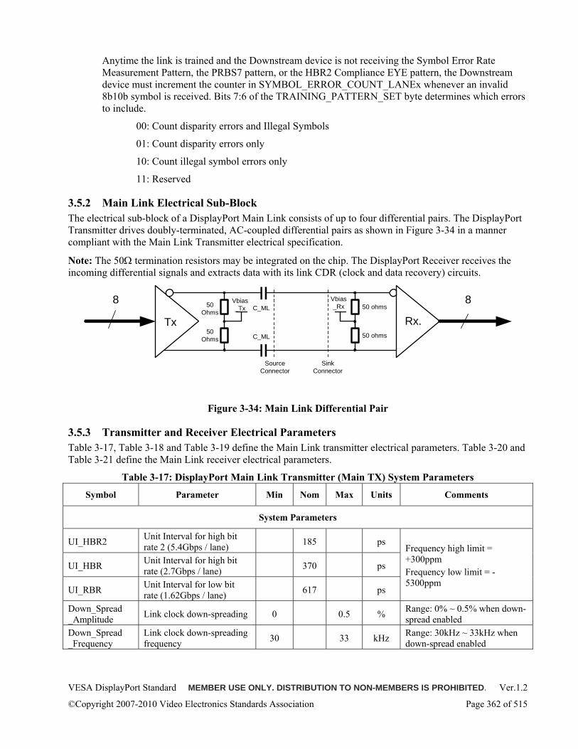
VESA DisplayPort Standard MEMBER USE ONLY. DISTRIBUTION TO NON-MEMBERS IS PROHIBITED. Ver.1.2
©Copyright 2007-2010 Video Electronics Standards Association Page 362 of 515
Anytime the link is trained and the Downstream device is not receiving the Symbol Error Rate Measurement Pattern, the PRBS7 pattern, or the HBR2 Compliance EYE pattern, the Downstream device must increment the counter in SYMBOL_ERROR_COUNT_LANEx whenever an invalid 8b10b symbol is received. Bits 7:6 of the TRAINING_PATTERN_SET byte determines which errors to include.
00: Count disparity errors and Illegal Symbols
01: Count disparity errors only
10: Count illegal symbol errors only
11: Reserved
3.5.2 Main Link Electrical Sub-Block The electrical sub-block of a DisplayPort Main Link consists of up to four differential pairs. The DisplayPort Transmitter drives doubly-terminated, AC-coupled differential pairs as shown in Figure 3-34 in a manner compliant with the Main Link Transmitter electrical specification.
Note: The 50Ω termination resistors may be integrated on the chip. The DisplayPort Receiver receives the incoming differential signals and extracts data with its link CDR (clock and data recovery) circuits.
50Ohms
50Ohms
50 ohms
50 ohms
8 8
Tx Rx.
Vbias_Tx
Vbias_RxC_ML
C_ML
SourceConnector
SinkConnector
Figure 3-34: Main Link Differential Pair
3.5.3 Transmitter and Receiver Electrical Parameters Table 3-17, Table 3-18 and Table 3-19 define the Main Link transmitter electrical parameters. Table 3-20 and Table 3-21 define the Main Link receiver electrical parameters.
Table 3-17: DisplayPort Main Link Transmitter (Main TX) System Parameters
Symbol Parameter Min Nom Max Units Comments
System Parameters
UI_HBR2 Unit Interval for high bit rate 2 (5.4Gbps / lane) 185 ps
UI_HBR Unit Interval for high bit rate (2.7Gbps / lane) 370 ps
UI_RBR Unit Interval for low bit rate (1.62Gbps / lane) 617 ps
Frequency high limit = +300ppm Frequency low limit = -5300ppm
Down_Spread _Amplitude Link clock down-spreading 0 0.5 % Range: 0% ~ 0.5% when down-
spread enabled Down_Spread _Frequency
Link clock down-spreading frequency 30 33 kHz Range: 30kHz ~ 33kHz when
down-spread enabled
VESA DisplayPort Standard MEMBER USE ONLY. DISTRIBUTION TO NON-MEMBERS IS PROHIBITED. Ver.1.2
©Copyright 2007-2010 Video Electronics Standards Association Page 363 of 515
Symbol Parameter Min Nom Max Units Comments
CTX AC Coupling Capacitor 75 200 nF
All DisplayPort Main Link lanes as well as AUX CH must be AC coupled. AC coupling capacitors must be placed on the transmitter side. Placement of AC coupling capacitors on the receiver side is optional.
Table 3-18: DisplayPort Main Link Transmitter (Main TX) TP2 Parameters
TP2 (TX External Connector – Normative)
Symbol Parameter Min Nom Max Units Comments
Ratio of Output Voltage Level 1/Level 0 0.8 6.0 dB
Ratio of Output Voltage Level 2/Level 1 0.1 5.1 dB VTX-OUTPUT-
RATIO_RBR_HBR Ratio of Output Voltage Level 3/Level 2 0.8 6.0 dB
Measured on non-transition bits at Pre-emphasis level 0 setting
Ratio of Output Voltage Level 2/Level 0 5.2 6.9 dB
Ratio of Output Voltage Level 2/Level 1 1.6 3.5 dB VTX-OUTPUT-
RATIO_HBR2 Ratio of Output Voltage Level 3/Level 2 1 4.4 dB
Measured on non-transition bits at Pre-emphasis level 0 setting
VTX-PREEMP-OFF Maximum Pre-emphasis when disabled 0.25 dB
Pre-emphasis Level 0 setting must not show any pre-emphasis at TP2 to prevent link training issues.
Delta of Pre-emphasis Level 1 vs. Level 0 2 dB
Delta of Pre-emphasis Level 2 vs. Level 1 1.6 dB VTX-PREEMP-DELTA
Delta of Pre-emphasis Level 3 vs. Level 2 1.6 dB
Applies to all valid voltage settings. Measured at Pre-emphasis Post Cursor2 Level 0. Support for Pre-emphasis Level 3 is optional.
Non-transition reduction Output Voltage Level 2 3 dB
Non-transition reduction Output Voltage Level 1 3 dB VTX-
DIFF_REDUCTION Non-transition reduction Output Voltage Level 0 1.4 dB
VTX_DIFF at each non-zero nominal pre-emphasis level must not be lower than the specified amount less than VTX_DIFF at the zero nominal pre-emphasis level.
Delta of Pre-emphasis Post Cursor2 Level 1 vs. Level 0 -0.45 dB VTX-PREEMP-POST2-
DELTA Delta of Pre-emphasis Post Cursor2 Level 2 vs. Level 1 -0.5 dB
Measured on 2nd TBIT at Pre-emphasis Level 0. Support for Pre-emphasis Post Cursor2 is optional.
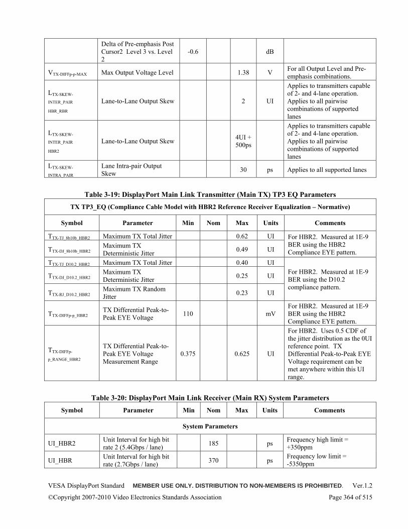
VESA DisplayPort Standard MEMBER USE ONLY. DISTRIBUTION TO NON-MEMBERS IS PROHIBITED. Ver.1.2
©Copyright 2007-2010 Video Electronics Standards Association Page 364 of 515
Delta of Pre-emphasis Post Cursor2 Level 3 vs. Level 2
-0.6 dB
VTX-DIFFp-p-MAX Max Output Voltage Level 1.38 V For all Output Level and Pre-emphasis combinations.
LTX-SKEW-
INTER_PAIR
HBR_RBR Lane-to-Lane Output Skew 2 UI
Applies to transmitters capable of 2- and 4-lane operation. Applies to all pairwise combinations of supported lanes
LTX-SKEW-
INTER_PAIR
HBR2 Lane-to-Lane Output Skew 4UI +
500ps
Applies to transmitters capable of 2- and 4-lane operation. Applies to all pairwise combinations of supported lanes
LTX-SKEW-
INTRA_PAIR Lane Intra-pair Output Skew 30 ps Applies to all supported lanes
Table 3-19: DisplayPort Main Link Transmitter (Main TX) TP3 EQ Parameters
TX TP3_EQ (Compliance Cable Model with HBR2 Reference Receiver Equalization – Normative)
Symbol Parameter Min Nom Max Units Comments
TTX-TJ_8b10b_HBR2 Maximum TX Total Jitter 0.62 UI
TTX-DJ_8b10b_HBR2 Maximum TX Deterministic Jitter 0.49 UI
For HBR2. Measured at 1E-9 BER using the HBR2 Compliance EYE pattern.
TTX-TJ_D10.2_HBR2 Maximum TX Total Jitter 0.40 UI
TTX-DJ_D10.2_HBR2 Maximum TX Deterministic Jitter 0.25 UI
TTX-RJ_D10.2_HBR2 Maximum TX Random Jitter 0.23 UI
For HBR2. Measured at 1E-9 BER using the D10.2 compliance pattern.
TTX-DIFFp-p_HBR2 TX Differential Peak-to-Peak EYE Voltage 110 mV
For HBR2. Measured at 1E-9 BER using the HBR2 Compliance EYE pattern.
TTX-DIFFp-
p_RANGE_HBR2
TX Differential Peak-to-Peak EYE Voltage Measurement Range
0.375 0.625 UI
For HBR2. Uses 0.5 CDF of the jitter distribution as the 0UI reference point. TX Differential Peak-to-Peak EYE Voltage requirement can be met anywhere within this UI range.
Table 3-20: DisplayPort Main Link Receiver (Main RX) System Parameters
Symbol Parameter Min Nom Max Units Comments
System Parameters
UI_HBR2 Unit Interval for high bit rate 2 (5.4Gbps / lane) 185 ps
UI_HBR Unit Interval for high bit rate (2.7Gbps / lane) 370 ps
Frequency high limit = +350ppm Frequency low limit = -5350ppm
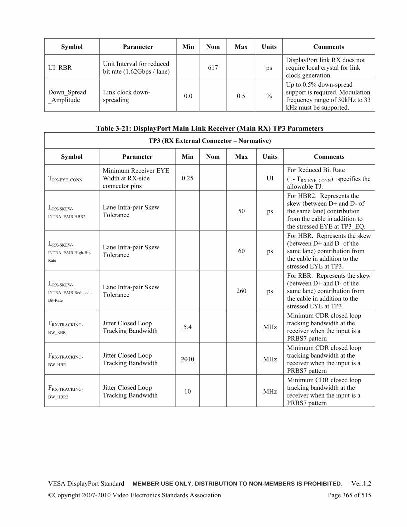
VESA DisplayPort Standard MEMBER USE ONLY. DISTRIBUTION TO NON-MEMBERS IS PROHIBITED. Ver.1.2
©Copyright 2007-2010 Video Electronics Standards Association Page 365 of 515
Symbol Parameter Min Nom Max Units Comments
UI_RBR Unit Interval for reduced bit rate (1.62Gbps / lane) 617 ps
DisplayPort link RX does not require local crystal for link clock generation.
Down_Spread _Amplitude
Link clock down- spreading 0.0 0.5 %
Up to 0.5% down-spread support is required. Modulation frequency range of 30kHz to 33 kHz must be supported.
Table 3-21: DisplayPort Main Link Receiver (Main RX) TP3 Parameters
TP3 (RX External Connector – Normative)
Symbol Parameter Min Nom Max Units Comments
TRX-EYE_CONN Minimum Receiver EYE Width at RX-side connector pins
0.25 UI For Reduced Bit Rate (1- TRX-EYE_CONN) specifies the allowable TJ.
LRX-SKEW-
INTRA_PAIR HBR2 Lane Intra-pair Skew Tolerance 50 ps
For HBR2. Represents the skew (between D+ and D- of the same lane) contribution from the cable in addition to the stressed EYE at TP3_EQ.
LRX-SKEW-
INTRA_PAIR High-Bit-
Rate
Lane Intra-pair Skew Tolerance 60 ps
For HBR. Represents the skew (between D+ and D- of the same lane) contribution from the cable in addition to the stressed EYE at TP3.
LRX-SKEW-
INTRA_PAIR Reduced-
Bit-Rate
Lane Intra-pair Skew Tolerance 260 ps
For RBR. Represents the skew (between D+ and D- of the same lane) contribution from the cable in addition to the stressed EYE at TP3.
FRX-TRACKING-
BW_RBR Jitter Closed Loop Tracking Bandwidth 5.4 MHz
Minimum CDR closed loop tracking bandwidth at the receiver when the input is a PRBS7 pattern
FRX-TRACKING-
BW_HBR Jitter Closed Loop Tracking Bandwidth 2010 MHz
Minimum CDR closed loop tracking bandwidth at the receiver when the input is a PRBS7 pattern
FRX-TRACKING-
BW_HBR2 Jitter Closed Loop Tracking Bandwidth 10 MHz
Minimum CDR closed loop tracking bandwidth at the receiver when the input is a PRBS7 pattern
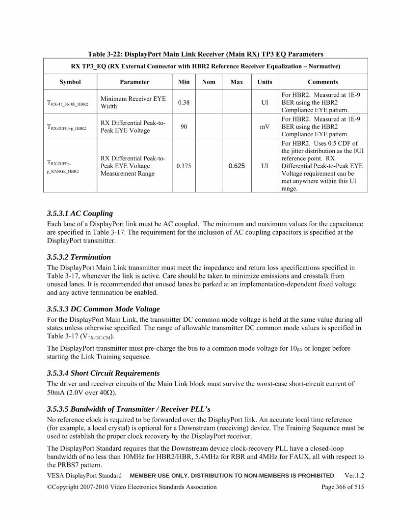
VESA DisplayPort Standard MEMBER USE ONLY. DISTRIBUTION TO NON-MEMBERS IS PROHIBITED. Ver.1.2
©Copyright 2007-2010 Video Electronics Standards Association Page 366 of 515
Table 3-22: DisplayPort Main Link Receiver (Main RX) TP3 EQ Parameters
RX TP3_EQ (RX External Connector with HBR2 Reference Receiver Equalization – Normative)
Symbol Parameter Min Nom Max Units Comments
TRX-TJ_8b10b_HBR2 Minimum Receiver EYE Width 0.38 UI
For HBR2. Measured at 1E-9 BER using the HBR2 Compliance EYE pattern.
TRX-DIFFp-p_HBR2 RX Differential Peak-to-Peak EYE Voltage 90 mV
For HBR2. Measured at 1E-9 BER using the HBR2 Compliance EYE pattern.
TRX-DIFFp-
p_RANGE_HBR2
RX Differential Peak-to-Peak EYE Voltage Measurement Range
0.375 0.625 UI
For HBR2. Uses 0.5 CDF of the jitter distribution as the 0UI reference point. RX Differential Peak-to-Peak EYE Voltage requirement can be met anywhere within this UI range.
3.5.3.1 AC Coupling Each lane of a DisplayPort link must be AC coupled. The minimum and maximum values for the capacitance are specified in Table 3-17. The requirement for the inclusion of AC coupling capacitors is specified at the DisplayPort transmitter.
3.5.3.2 Termination The DisplayPort Main Link transmitter must meet the impedance and return loss specifications specified in Table 3-17, whenever the link is active. Care should be taken to minimize emissions and crosstalk from unused lanes. It is recommended that unused lanes be parked at an implementation-dependent fixed voltage and any active termination be enabled.
3.5.3.3 DC Common Mode Voltage For the DisplayPort Main Link, the transmitter DC common mode voltage is held at the same value during all states unless otherwise specified. The range of allowable transmitter DC common mode values is specified in Table 3-17 (VTX-DC-CM).
The DisplayPort transmitter must pre-charge the bus to a common mode voltage for 10μs or longer before starting the Link Training sequence.
3.5.3.4 Short Circuit Requirements The driver and receiver circuits of the Main Link block must survive the worst-case short-circuit current of 50mA (2.0V over 40Ω).
3.5.3.5 Bandwidth of Transmitter / Receiver PLL’s No reference clock is required to be forwarded over the DisplayPort link. An accurate local time reference (for example, a local crystal) is optional for a Downstream (receiving) device. The Training Sequence must be used to establish the proper clock recovery by the DisplayPort receiver.
The DisplayPort Standard requires that the Downstream device clock-recovery PLL have a closed-loop bandwidth of no less than 10MHz for HBR2/HBR, 5.4MHz for RBR and 4MHz for FAUX, all with respect to the PRBS7 pattern.
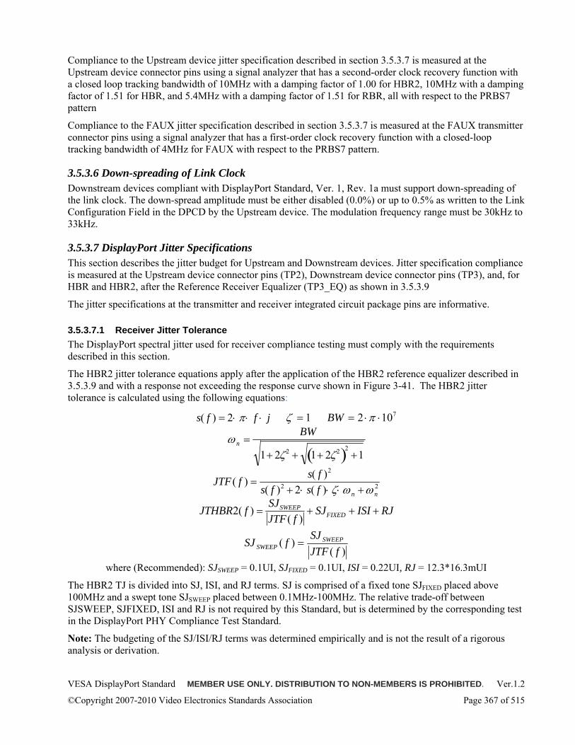
VESA DisplayPort Standard MEMBER USE ONLY. DISTRIBUTION TO NON-MEMBERS IS PROHIBITED. Ver.1.2
©Copyright 2007-2010 Video Electronics Standards Association Page 367 of 515
Compliance to the Upstream device jitter specification described in section 3.5.3.7 is measured at the Upstream device connector pins using a signal analyzer that has a second-order clock recovery function with a closed loop tracking bandwidth of 10MHz with a damping factor of 1.00 for HBR2, 10MHz with a damping factor of 1.51 for HBR, and 5.4MHz with a damping factor of 1.51 for RBR, all with respect to the PRBS7 pattern
Compliance to the FAUX jitter specification described in section 3.5.3.7 is measured at the FAUX transmitter connector pins using a signal analyzer that has a first-order clock recovery function with a closed-loop tracking bandwidth of 4MHz for FAUX with respect to the PRBS7 pattern.
3.5.3.6 Down-spreading of Link Clock Downstream devices compliant with DisplayPort Standard, Ver. 1, Rev. 1a must support down-spreading of the link clock. The down-spread amplitude must be either disabled (0.0%) or up to 0.5% as written to the Link Configuration Field in the DPCD by the Upstream device. The modulation frequency range must be 30kHz to 33kHz.
3.5.3.7 DisplayPort Jitter Specifications This section describes the jitter budget for Upstream and Downstream devices. Jitter specification compliance is measured at the Upstream device connector pins (TP2), Downstream device connector pins (TP3), and, for HBR and HBR2, after the Reference Receiver Equalizer (TP3_EQ) as shown in 3.5.3.9
The jitter specifications at the transmitter and receiver integrated circuit package pins are informative.
3.5.3.7.1 Receiver Jitter Tolerance The DisplayPort spectral jitter used for receiver compliance testing must comply with the requirements described in this section.
The HBR2 jitter tolerance equations apply after the application of the HBR2 reference equalizer described in 3.5.3.9 and with a response not exceeding the response curve shown in Figure 3-41. The HBR2 jitter tolerance is calculated using the following equations:
s( f ) = 2⋅ π⋅ f ⋅ j 1=ζ 7102 ⋅⋅= πBW
ω n =BW
1+ 2ζ2 + 1+ 2ζ2( )2+1
JTF( f ) =s( f )2
s( f )2 + 2⋅ s( f )⋅ ζ⋅ ω n +ω n2
JTHBR2( f ) =SJSWEEP
JTF( f )+ SJFIXED + ISI + RJ
)()(
fJTFSJ
fSJ SWEEPSWEEP =
where (Recommended): SJSWEEP = 0.1UI, SJFIXED = 0.1UI, ISI = 0.22UI, RJ = 12.3*16.3mUI
The HBR2 TJ is divided into SJ, ISI, and RJ terms. SJ is comprised of a fixed tone SJFIXED placed above 100MHz and a swept tone SJSWEEP placed between 0.1MHz-100MHz. The relative trade-off between SJSWEEP, SJFIXED, ISI and RJ is not required by this Standard, but is determined by the corresponding test in the DisplayPort PHY Compliance Test Standard.
Note: The budgeting of the SJ/ISI/RJ terms was determined empirically and is not the result of a rigorous analysis or derivation.
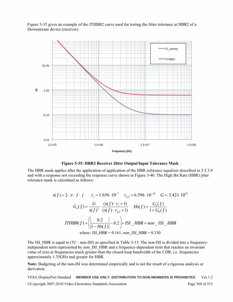
VESA DisplayPort Standard MEMBER USE ONLY. DISTRIBUTION TO NON-MEMBERS IS PROHIBITED. Ver.1.2
©Copyright 2007-2010 Video Electronics Standards Association Page 368 of 515
Figure 3-35 gives an example of the JTHBR2 curve used for testing the Jitter tolerance at HBR2 of a Downstream device (receiver).
Figure 3-35: HBR2 Receiver Jitter Output/Input Tolerance Mask
The HBR mask applies after the application of application of the HBR reference equalizer described in 3.5.3.9 and with a response not exceeding the response curve shown in Figure 3-40. The High Bit Rate (HBR) jitter tolerance mask is calculated as follows:
s( f ) = 2 ⋅ π ⋅ f ⋅ j τ z =1.656 ⋅10−7 τ p2 = 6.596 ⋅10−10 G = 3.421⋅ 1014
Go( f ) =G
s( f )2 ⋅(s( f ) ⋅ τ z +1)(s( f ) ⋅ τ p2 +1)
Hs( f ) =Go( f )
1+ G0( f )
JTHBR( f ) =0.2
1− Hs( f )− 0.2
⎛
⎝ ⎜
⎞
⎠ ⎟ + ISI _ HBR + non _ ISI _ HBR
where: ISI_HBR = 0.161, non_ISI_HBR = 0.330 The ISI_HBR is equal to (TJ – non-ISI) as specified in Table 3-13. The non-ISI is divided into a frequency-independent term represented by non_ISI_HBR and a frequency-dependent term that reaches an invariant value of zero at frequencies much greater than the closed-loop bandwidth of the CDR, i.e. frequencies approximately 1.35GHz and greater for HBR.
Note: Budgeting of the non-ISI was determined empirically and is not the result of a rigorous analysis or derivation.
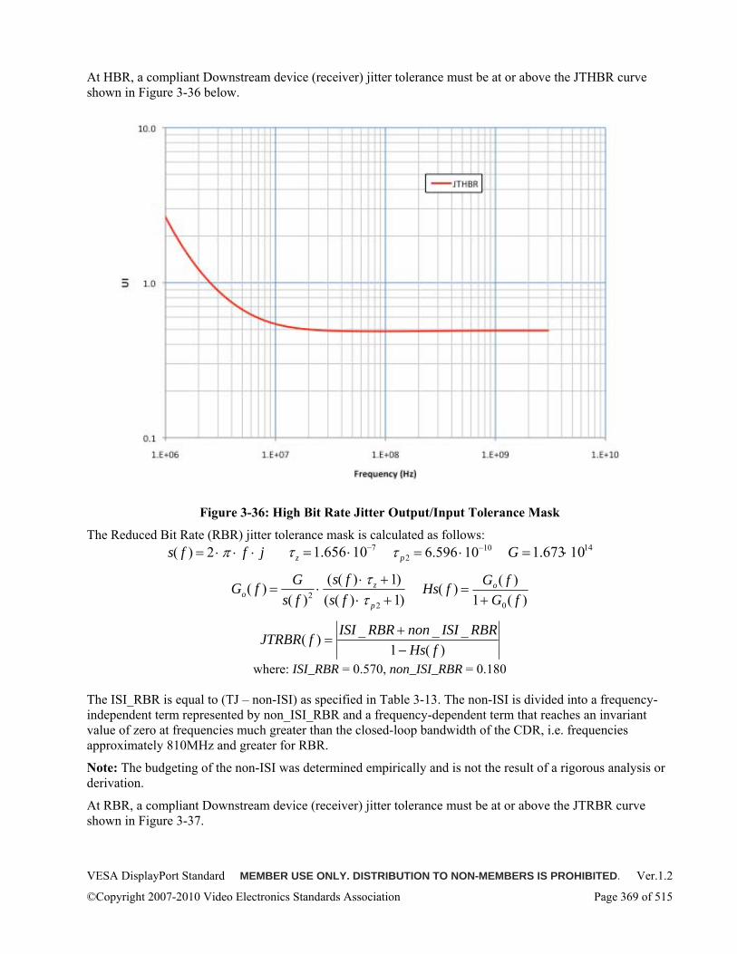
VESA DisplayPort Standard MEMBER USE ONLY. DISTRIBUTION TO NON-MEMBERS IS PROHIBITED. Ver.1.2
©Copyright 2007-2010 Video Electronics Standards Association Page 369 of 515
At HBR, a compliant Downstream device (receiver) jitter tolerance must be at or above the JTHBR curve shown in Figure 3-36 below.
Figure 3-36: High Bit Rate Jitter Output/Input Tolerance Mask
The Reduced Bit Rate (RBR) jitter tolerance mask is calculated as follows: s( f ) = 2 ⋅ π ⋅ f ⋅ j τ z =1.656 ⋅10−7 τ p2 = 6.596 ⋅10−10 G =1.673⋅ 1014
Go( f ) =G
s( f )2 ⋅(s( f ) ⋅ τ z +1)(s( f ) ⋅ τ p2 +1)
Hs( f ) =Go( f )
1+ G0( f )
JTRBR( f ) =ISI _ RBR + non _ ISI _ RBR
1 − Hs( f )
where: ISI_RBR = 0.570, non_ISI_RBR = 0.180 The ISI_RBR is equal to (TJ – non-ISI) as specified in Table 3-13. The non-ISI is divided into a frequency-independent term represented by non_ISI_RBR and a frequency-dependent term that reaches an invariant value of zero at frequencies much greater than the closed-loop bandwidth of the CDR, i.e. frequencies approximately 810MHz and greater for RBR.
Note: The budgeting of the non-ISI was determined empirically and is not the result of a rigorous analysis or derivation.
At RBR, a compliant Downstream device (receiver) jitter tolerance must be at or above the JTRBR curve shown in Figure 3-37.
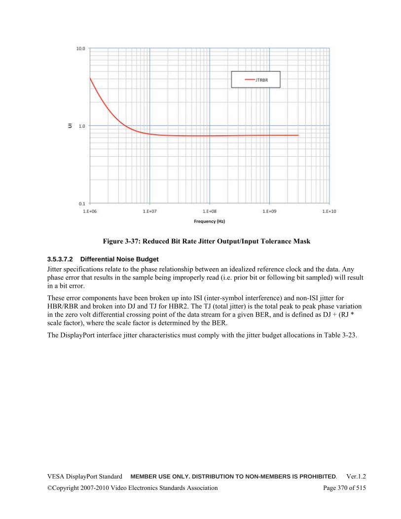
VESA DisplayPort Standard MEMBER USE ONLY. DISTRIBUTION TO NON-MEMBERS IS PROHIBITED. Ver.1.2
©Copyright 2007-2010 Video Electronics Standards Association Page 370 of 515
Figure 3-37: Reduced Bit Rate Jitter Output/Input Tolerance Mask
3.5.3.7.2 Differential Noise Budget Jitter specifications relate to the phase relationship between an idealized reference clock and the data. Any phase error that results in the sample being improperly read (i.e. prior bit or following bit sampled) will result in a bit error.
These error components have been broken up into ISI (inter-symbol interference) and non-ISI jitter for HBR/RBR and broken into DJ and TJ for HBR2. The TJ (total jitter) is the total peak to peak phase variation in the zero volt differential crossing point of the data stream for a given BER, and is defined as DJ + (RJ * scale factor), where the scale factor is determined by the BER.
The DisplayPort interface jitter characteristics must comply with the jitter budget allocations in Table 3-23.
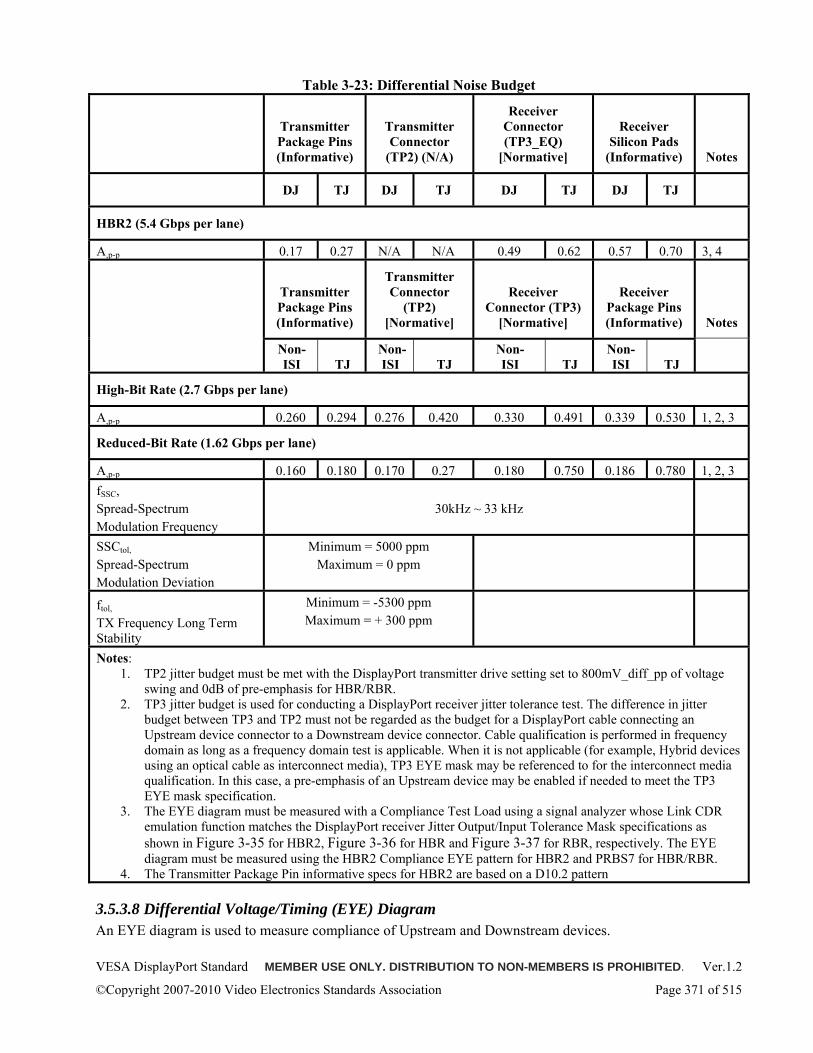
VESA DisplayPort Standard MEMBER USE ONLY. DISTRIBUTION TO NON-MEMBERS IS PROHIBITED. Ver.1.2
©Copyright 2007-2010 Video Electronics Standards Association Page 371 of 515
Table 3-23: Differential Noise Budget
Transmitter Package Pins (Informative)
Transmitter Connector
(TP2) (N/A)
Receiver Connector (TP3_EQ)
[Normative]
Receiver Silicon Pads
(Informative) Notes
DJ TJ DJ TJ DJ TJ DJ TJ
HBR2 (5.4 Gbps per lane)
A,p-p 0.17 0.27 N/A N/A 0.49 0.62 0.57 0.70 3, 4
Transmitter Package Pins (Informative)
Transmitter Connector
(TP2) [Normative]
Receiver Connector (TP3)
[Normative]
Receiver Package Pins (Informative) Notes
Non- ISI TJ
Non-ISI TJ
Non- ISI TJ
Non- ISI TJ
High-Bit Rate (2.7 Gbps per lane)
A,p-p 0.260 0.294 0.276 0.420 0.330 0.491 0.339 0.530 1, 2, 3
Reduced-Bit Rate (1.62 Gbps per lane)
A,p-p 0.160 0.180 0.170 0.27 0.180 0.750 0.186 0.780 1, 2, 3 fSSC, Spread-Spectrum Modulation Frequency
30kHz ~ 33 kHz
SSCtol,
Spread-Spectrum Modulation Deviation
Minimum = 5000 ppm Maximum = 0 ppm
ftol,
TX Frequency Long Term Stability
Minimum = -5300 ppm Maximum = + 300 ppm
Notes: 1. TP2 jitter budget must be met with the DisplayPort transmitter drive setting set to 800mV_diff_pp of voltage
swing and 0dB of pre-emphasis for HBR/RBR. 2. TP3 jitter budget is used for conducting a DisplayPort receiver jitter tolerance test. The difference in jitter
budget between TP3 and TP2 must not be regarded as the budget for a DisplayPort cable connecting an Upstream device connector to a Downstream device connector. Cable qualification is performed in frequency domain as long as a frequency domain test is applicable. When it is not applicable (for example, Hybrid devices using an optical cable as interconnect media), TP3 EYE mask may be referenced to for the interconnect media qualification. In this case, a pre-emphasis of an Upstream device may be enabled if needed to meet the TP3 EYE mask specification.
3. The EYE diagram must be measured with a Compliance Test Load using a signal analyzer whose Link CDR emulation function matches the DisplayPort receiver Jitter Output/Input Tolerance Mask specifications as shown in Figure 3-35 for HBR2, Figure 3-36 for HBR and Figure 3-37 for RBR, respectively. The EYE diagram must be measured using the HBR2 Compliance EYE pattern for HBR2 and PRBS7 for HBR/RBR.
4. The Transmitter Package Pin informative specs for HBR2 are based on a D10.2 pattern
3.5.3.8 Differential Voltage/Timing (EYE) Diagram An EYE diagram is used to measure compliance of Upstream and Downstream devices.
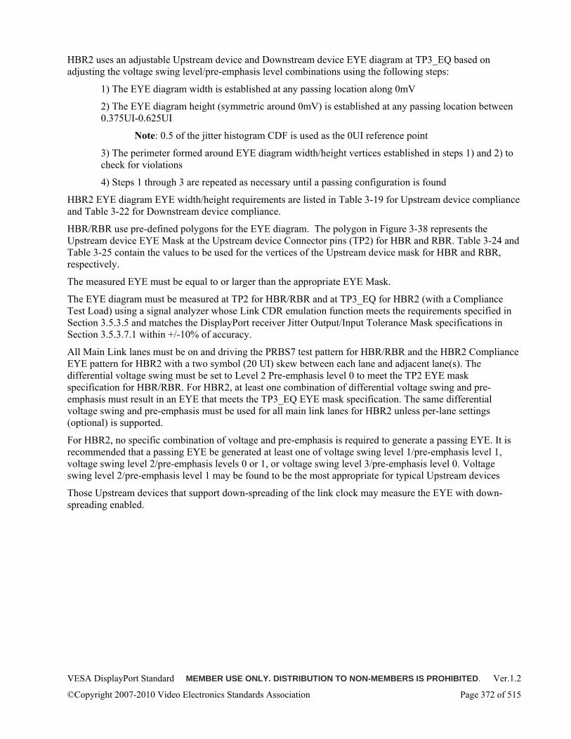
VESA DisplayPort Standard MEMBER USE ONLY. DISTRIBUTION TO NON-MEMBERS IS PROHIBITED. Ver.1.2
©Copyright 2007-2010 Video Electronics Standards Association Page 372 of 515
HBR2 uses an adjustable Upstream device and Downstream device EYE diagram at TP3_EQ based on adjusting the voltage swing level/pre-emphasis level combinations using the following steps:
1) The EYE diagram width is established at any passing location along 0mV
2) The EYE diagram height (symmetric around 0mV) is established at any passing location between 0.375UI-0.625UI
Note: 0.5 of the jitter histogram CDF is used as the 0UI reference point
3) The perimeter formed around EYE diagram width/height vertices established in steps 1) and 2) to check for violations
4) Steps 1 through 3 are repeated as necessary until a passing configuration is found
HBR2 EYE diagram EYE width/height requirements are listed in Table 3-19 for Upstream device compliance and Table 3-22 for Downstream device compliance.
HBR/RBR use pre-defined polygons for the EYE diagram. The polygon in Figure 3-38 represents the Upstream device EYE Mask at the Upstream device Connector pins (TP2) for HBR and RBR. Table 3-24 and Table 3-25 contain the values to be used for the vertices of the Upstream device mask for HBR and RBR, respectively.
The measured EYE must be equal to or larger than the appropriate EYE Mask.
The EYE diagram must be measured at TP2 for HBR/RBR and at TP3_EQ for HBR2 (with a Compliance Test Load) using a signal analyzer whose Link CDR emulation function meets the requirements specified in Section 3.5.3.5 and matches the DisplayPort receiver Jitter Output/Input Tolerance Mask specifications in Section 3.5.3.7.1 within +/-10% of accuracy.
All Main Link lanes must be on and driving the PRBS7 test pattern for HBR/RBR and the HBR2 Compliance EYE pattern for HBR2 with a two symbol (20 UI) skew between each lane and adjacent lane(s). The differential voltage swing must be set to Level 2 Pre-emphasis level 0 to meet the TP2 EYE mask specification for HBR/RBR. For HBR2, at least one combination of differential voltage swing and pre-emphasis must result in an EYE that meets the TP3_EQ EYE mask specification. The same differential voltage swing and pre-emphasis must be used for all main link lanes for HBR2 unless per-lane settings (optional) is supported.
For HBR2, no specific combination of voltage and pre-emphasis is required to generate a passing EYE. It is recommended that a passing EYE be generated at least one of voltage swing level 1/pre-emphasis level 1, voltage swing level 2/pre-emphasis levels 0 or 1, or voltage swing level 3/pre-emphasis level 0. Voltage swing level 2/pre-emphasis level 1 may be found to be the most appropriate for typical Upstream devices
Those Upstream devices that support down-spreading of the link clock may measure the EYE with down-spreading enabled.
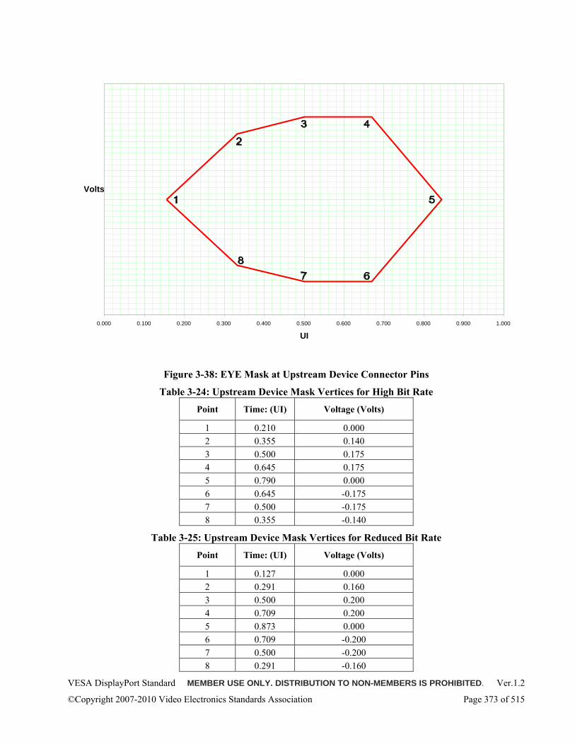
VESA DisplayPort Standard MEMBER USE ONLY. DISTRIBUTION TO NON-MEMBERS IS PROHIBITED. Ver.1.2
©Copyright 2007-2010 Video Electronics Standards Association Page 373 of 515
Figure 3-38: EYE Mask at Upstream Device Connector Pins
Table 3-24: Upstream Device Mask Vertices for High Bit Rate
Point Time: (UI) Voltage (Volts)
1 0.210 0.000 2 0.355 0.140 3 0.500 0.175 4 0.645 0.175 5 0.790 0.000 6 0.645 -0.175 7 0.500 -0.175 8 0.355 -0.140
Table 3-25: Upstream Device Mask Vertices for Reduced Bit Rate
Point Time: (UI) Voltage (Volts)
1 0.127 0.000 2 0.291 0.160 3 0.500 0.200 4 0.709 0.200 5 0.873 0.000 6 0.709 -0.200 7 0.500 -0.200 8 0.291 -0.160
0.000 0.100 0.200 0.300 0.400 0.500 0.600 0.700 0.800 0.900 1.000
UI
Volts
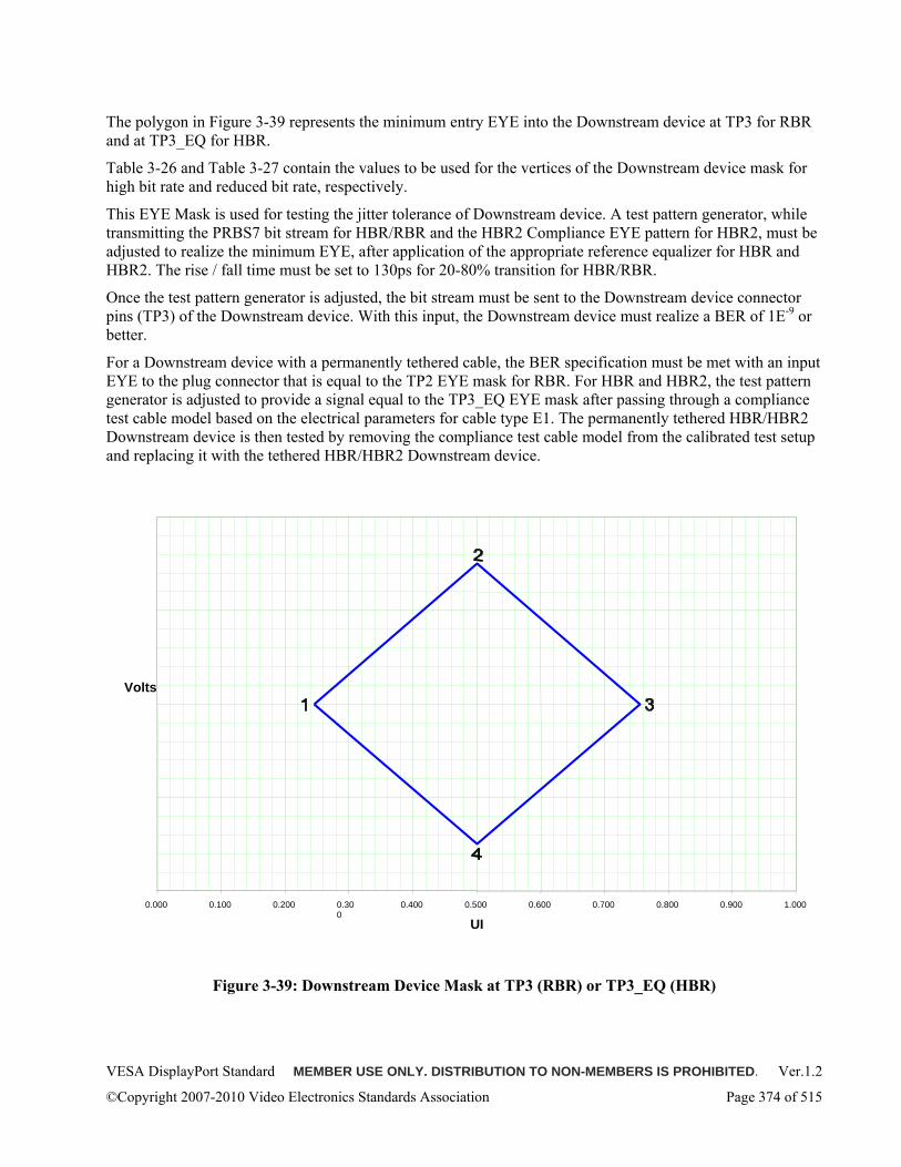
VESA DisplayPort Standard MEMBER USE ONLY. DISTRIBUTION TO NON-MEMBERS IS PROHIBITED. Ver.1.2
©Copyright 2007-2010 Video Electronics Standards Association Page 374 of 515
The polygon in Figure 3-39 represents the minimum entry EYE into the Downstream device at TP3 for RBR and at TP3_EQ for HBR.
Table 3-26 and Table 3-27 contain the values to be used for the vertices of the Downstream device mask for high bit rate and reduced bit rate, respectively.
This EYE Mask is used for testing the jitter tolerance of Downstream device. A test pattern generator, while transmitting the PRBS7 bit stream for HBR/RBR and the HBR2 Compliance EYE pattern for HBR2, must be adjusted to realize the minimum EYE, after application of the appropriate reference equalizer for HBR and HBR2. The rise / fall time must be set to 130ps for 20-80% transition for HBR/RBR.
Once the test pattern generator is adjusted, the bit stream must be sent to the Downstream device connector pins (TP3) of the Downstream device. With this input, the Downstream device must realize a BER of 1E-9 or better.
For a Downstream device with a permanently tethered cable, the BER specification must be met with an input EYE to the plug connector that is equal to the TP2 EYE mask for RBR. For HBR and HBR2, the test pattern generator is adjusted to provide a signal equal to the TP3_EQ EYE mask after passing through a compliance test cable model based on the electrical parameters for cable type E1. The permanently tethered HBR/HBR2 Downstream device is then tested by removing the compliance test cable model from the calibrated test setup and replacing it with the tethered HBR/HBR2 Downstream device.
Figure 3-39: Downstream Device Mask at TP3 (RBR) or TP3_EQ (HBR)
0.000 0.100 0.200 0.300 0.400 0.500 0.600 0.700 0.800 0.900 1.000
UI
Volts
VESA DisplayPort Standard MEMBER USE ONLY. DISTRIBUTION TO NON-MEMBERS IS PROHIBITED. Ver.1.2
©Copyright 2007-2010 Video Electronics Standards Association Page 375 of 515
Table 3-26: Downstream Device EYE Vertices for TP3_EQ at High Bit Rate
Point Time: (UI) Voltage (Volts)
1 0.246 0.000 2 0.500 0.075 3 0.755 0.000 4 0.500 -0.075
Table 3-27: Downstream Device EYE Vertices at TP3 for Reduced Bit Rate
Point Time: (UI) Voltage (Volts)
1 0.375 0.000 2 0.500 0.023 3 0.625 0.000 4 0.500 -0.023
3.5.3.9 Reference Equalizers The HBR and HBR2 EYE diagrams are defined after application of a corresponding reference equalizer with a response curve as defined below. The Reference Receiver Equalizer’s primary function is to open the EYE for compliance measurements and does not define the Downstream Device Receiver Equalizer implementation. A Downstream device that implements receiver equalization similar to the Reference Receiver Equalizer is not guaranteed to pass Downstream device Compliance tests.
Note: the application of an equalizer with a response curve at the receiver may degrade the receive EYE in some configurations. It is recommended that an equalizer be designed to adapt to the received signal during link training with a maximum response granularity of 2dB @ 1.35GHz (HBR) or 2dB @ 2.7GHz (HBR2).
The HBR Reference Receiver Equalizer is modeled as a continuous time linear equalizer (CTLE) with a zero at 700MHz and poles at 1.35GHz and 2.5GHz, see Figure 3-40.
The HBR Reference Equalizer transfer function is given by
H(s) =ω p1ω p 2
ωz
⋅s + ωz
(s + ω p1)(s + ω p 2)
which has magnitude given by
H( jω) =ω p1ω p 2
ωz
⋅ω 2 + ωz
2
ω 2 + ω p12 ⋅ ω 2 + ω p 2
2
where
ωz = 2π (0.7 ×10⁹)
ω p1 = 2π (1.35 ×10⁹)
ω p 2 = 2π (2.5 ×10⁹)
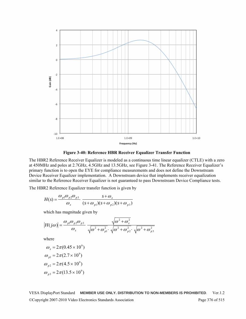
VESA DisplayPort Standard MEMBER USE ONLY. DISTRIBUTION TO NON-MEMBERS IS PROHIBITED. Ver.1.2
©Copyright 2007-2010 Video Electronics Standards Association Page 376 of 515
Figure 3-40: Reference HBR Receiver Equalizer Transfer Function
The HBR2 Reference Receiver Equalizer is modeled as a continuous time linear equalizer (CTLE) with a zero at 450MHz and poles at 2.7GHz, 4.5GHz and 13.5GHz, see Figure 3-41. The Reference Receiver Equalizer’s primary function is to open the EYE for compliance measurements and does not define the Downstream Device Receiver Equalizer implementation. A Downstream device that implements receiver equalization similar to the Reference Receiver Equalizer is not guaranteed to pass Downstream Device Compliance tests.
The HBR2 Reference Equalizer transfer function is given by
H(s) =ω p1ω p 2ω p 3
ω z
⋅s +ω z
(s +ω p1)(s +ω p 2)(s +ω p 3)
which has magnitude given by
H( jω) =ω p1ω p 2ω p 3
ω z
⋅ω 2 +ω z
2
ω 2 +ω p12 ⋅ ω 2 +ω p 2
2 ⋅ ω 2 +ω p 32
where
ω z = 2π (0.45 ×10⁹)
ω p1 = 2π (2.7 ×10⁹)
ω p 2 = 2π (4.5 ×10⁹)
ω p 3 = 2π (13.5 ×10⁹)
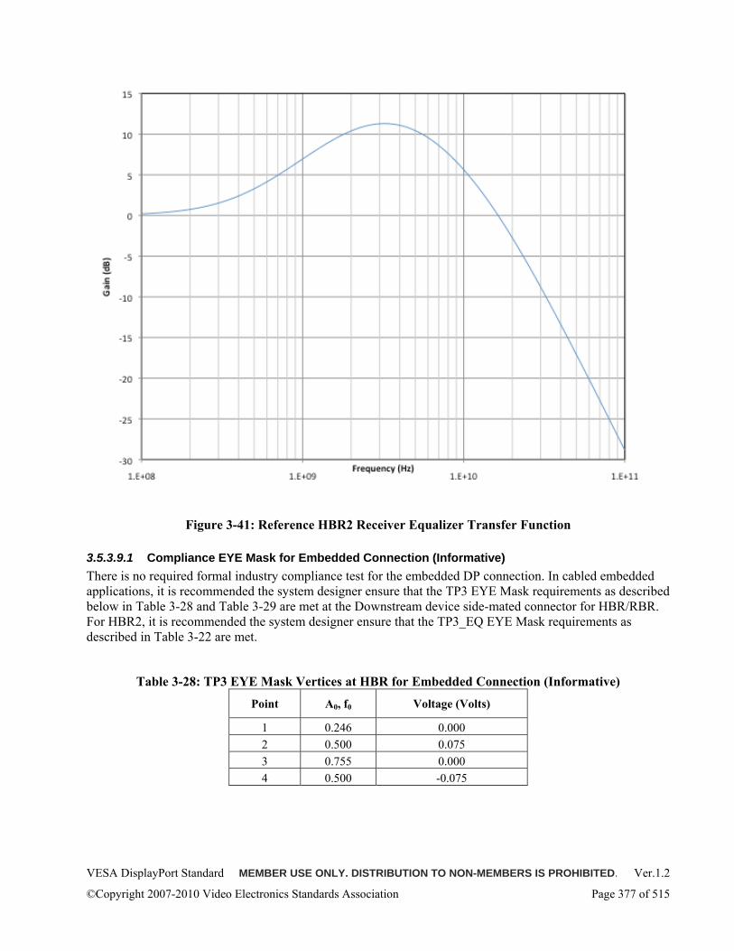
VESA DisplayPort Standard MEMBER USE ONLY. DISTRIBUTION TO NON-MEMBERS IS PROHIBITED. Ver.1.2
©Copyright 2007-2010 Video Electronics Standards Association Page 377 of 515
Figure 3-41: Reference HBR2 Receiver Equalizer Transfer Function
3.5.3.9.1 Compliance EYE Mask for Embedded Connection (Informative) There is no required formal industry compliance test for the embedded DP connection. In cabled embedded applications, it is recommended the system designer ensure that the TP3 EYE Mask requirements as described below in Table 3-28 and Table 3-29 are met at the Downstream device side-mated connector for HBR/RBR. For HBR2, it is recommended the system designer ensure that the TP3_EQ EYE Mask requirements as described in Table 3-22 are met.
Table 3-28: TP3 EYE Mask Vertices at HBR for Embedded Connection (Informative)
Point A0, f0 Voltage (Volts)
1 0.246 0.000 2 0.500 0.075 3 0.755 0.000 4 0.500 -0.075
VESA DisplayPort Standard MEMBER USE ONLY. DISTRIBUTION TO NON-MEMBERS IS PROHIBITED. Ver.1.2
©Copyright 2007-2010 Video Electronics Standards Association Page 378 of 515
Table 3-29: TP3 EYE Mask Vertices for RBR for Embedded Connection (Informative)
Point A0, f0 Voltage (Volts)
1 0.270 0.000 2 0.500 0.068 3 0.731 0.000 4 0.500 -0.068
3.5.3.10 Loss over Upstream Device Interconnect The Upstream device interconnect is the trace route between the Main Link transmitter integrated circuit package pins and the Upstream device connector pins (TP2).
The impedance of the Upstream device interconnect should be matched to the impedance of the connector and cable assembly so as to minimize return loss and maximize the transmitted signal. Failure to properly match the impedances will reduce the EYE opening decreasing the allowable Upstream device interconnect trace length.
Protection devices should add no more than 1.5pF parasitic load to each trace. Series protection resistors are not recommended. Losses are demonstrated by an EYE measurement at the Upstream device connector (TP2) for HBR/RBR and at TP3_EQ for HBR2.
Note: The approximate maximum length is 304.8mm (12 inches) using high volume manufacturing PCB materials. It is recommended that no more than two vias per trace be used.
3.5.3.11 Loss over Downstream Device Interconnect The Downstream device interconnect is the trace route between the Downstream device connector pins and Main Link receiver integrated circuit package pins.
The impedance of the Downstream device interconnect should be matched to the impedance of the connector and cable assembly so as to minimize return loss and maximize the transmitted signal. Failure to properly match the impedances will reduce the EYE opening decreasing the allowable Downstream device interconnect trace length.
Protection devices should add no more than 1.5pF parasitic load to each trace. Series protection resistors are not recommended.
Note: The approximate maximum length is 50.8mm (two inches) using high volume manufacturing PCB materials. It is recommended that no more than two vias per trace be used.
3.5.4 ESD and EOS Protection All signal and power pins of associated DisplayPort components (transmitter IC, receiver IC, and associated I/O circuitry) must withstand at least JEDEC JESD22-A114-B Class 2 (2kV Human Body Model, 200V Machine Model) strikes.
DisplayPort devices implementing this specification may swing the I/O lines as high as ± 0.3V single-ended with respect the common mode bias reference level. The designer must carefully select clamping devices and clamping rail voltages such that ESD devices will not cause clipping of normal signals.
VESA DisplayPort Standard MEMBER USE ONLY. DISTRIBUTION TO NON-MEMBERS IS PROHIBITED. Ver.1.2
©Copyright 2007-2010 Video Electronics Standards Association Page 379 of 515
4 Mechanical This section describes the mechanical specifications of a DisplayPort link. Cable assembly specification for external connection and connector specification are covered in this section6. Applications requiring a larger or longer box-to-box application space than supported by a passive cable assembly as defined in this section may be supported by the use of an active Hybrid device or any other such device as provided for under Section 2.1.4. The interfaces of these devices must meet the interface requirements of a Source and Sink respectively.
4.1 Cable-Connector Assembly Specifications (for box-to-box) The cable assembly specification is divided into two categories reflecting the high bit rates (2.7Gbps and 5.4Gbps per lane) and the low bit rate (1.62Gbps per lane), respectively.
The high bit rate specification generally has higher performance electrical requirements and is usually represented by one or more of the following: shorter lengths, larger wire gauges, lower dielectric loss insulation materials.
The low bit rate specification generally has lower performance electrical requirements and is usually represented by one or more of the following: longer lengths, smaller wire gauges, higher dielectric loss insulation materials.
Among the cable-connector assembly parameters, IL (insertion loss), RL (reflection loss), skew (both intra-pair and inter-pair), and Near-End Noise (NEN) differ between high bit rate and low bit rate specifications. The PSELFEN (power sum equal level far-end noise) parameter applies to the high bit rate cable assembly specification only.
Both categories represent the box-to-box application space sometimes referred to as external/desktop and consumer electronics (CE).
The embedded cable application space which is characterized by its inaccessibility to the end-user and is sometimes referred to as internal/mobile is not explicitly specified here. Instead, the system integrator is required to meet the EYE mask requirements at the receiver pins by making appropriate trade-offs between circuit trace performance and cabling performance.
In general the high bit rate and low bit rate electrical specification presented below still apply to the internal/mobile cable assemblies given the same PCB traces at both ends of the channel except that the physical dimensions are much smaller.
6 Masks for insertion loss, reflection loss, near-end noise, and far-end noise, and the impedance profile in this section were generated by Tyco Electronics. Channel simulations were run to verify that the worst-case cable-connector assembly as represented by those masks would meet receiver EYE masks specified in this document.
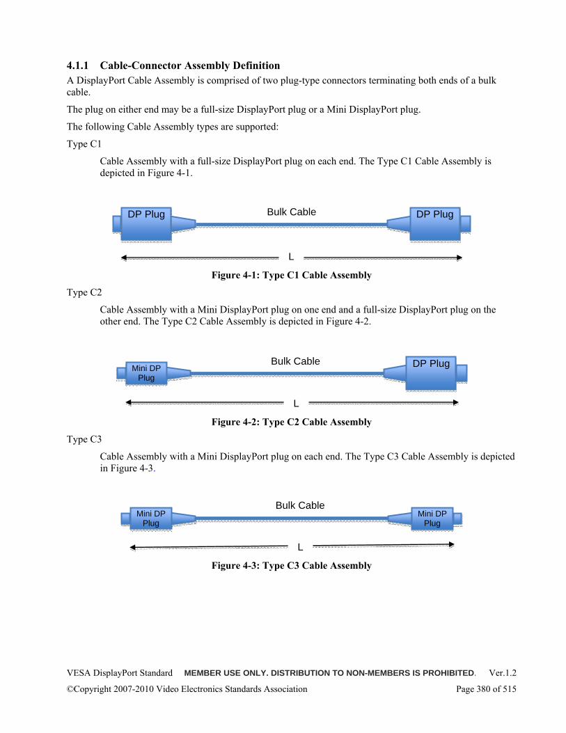
VESA DisplayPort Standard MEMBER USE ONLY. DISTRIBUTION TO NON-MEMBERS IS PROHIBITED. Ver.1.2
©Copyright 2007-2010 Video Electronics Standards Association Page 380 of 515
4.1.1 Cable-Connector Assembly Definition A DisplayPort Cable Assembly is comprised of two plug-type connectors terminating both ends of a bulk cable.
The plug on either end may be a full-size DisplayPort plug or a Mini DisplayPort plug.
The following Cable Assembly types are supported:
Type C1
Cable Assembly with a full-size DisplayPort plug on each end. The Type C1 Cable Assembly is depicted in Figure 4-1.
Figure 4-1: Type C1 Cable Assembly
Type C2
Cable Assembly with a Mini DisplayPort plug on one end and a full-size DisplayPort plug on the other end. The Type C2 Cable Assembly is depicted in Figure 4-2.
Figure 4-2: Type C2 Cable Assembly
Type C3
Cable Assembly with a Mini DisplayPort plug on each end. The Type C3 Cable Assembly is depicted in Figure 4-3.
Figure 4-3: Type C3 Cable Assembly
DP Plug Bulk Cable
L
DP Plug
Mini DP Plug
Bulk Cable
L
DP Plug
Bulk Cable
L
Mini DP Plug
Mini DP Plug
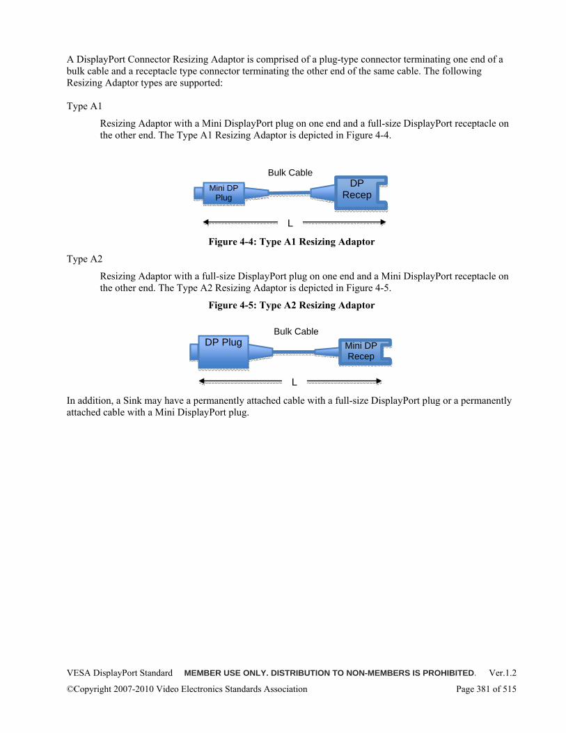
VESA DisplayPort Standard MEMBER USE ONLY. DISTRIBUTION TO NON-MEMBERS IS PROHIBITED. Ver.1.2
©Copyright 2007-2010 Video Electronics Standards Association Page 381 of 515
A DisplayPort Connector Resizing Adaptor is comprised of a plug-type connector terminating one end of a bulk cable and a receptacle type connector terminating the other end of the same cable. The following Resizing Adaptor types are supported: Type A1
Resizing Adaptor with a Mini DisplayPort plug on one end and a full-size DisplayPort receptacle on the other end. The Type A1 Resizing Adaptor is depicted in Figure 4-4.
Figure 4-4: Type A1 Resizing Adaptor
Type A2
Resizing Adaptor with a full-size DisplayPort plug on one end and a Mini DisplayPort receptacle on the other end. The Type A2 Resizing Adaptor is depicted in Figure 4-5.
Figure 4-5: Type A2 Resizing Adaptor
In addition, a Sink may have a permanently attached cable with a full-size DisplayPort plug or a permanently attached cable with a Mini DisplayPort plug.
Bulk Cable
L
Mini DP Plug
DP Recep
Bulk Cable
L
Mini DP Recep
DP Plug
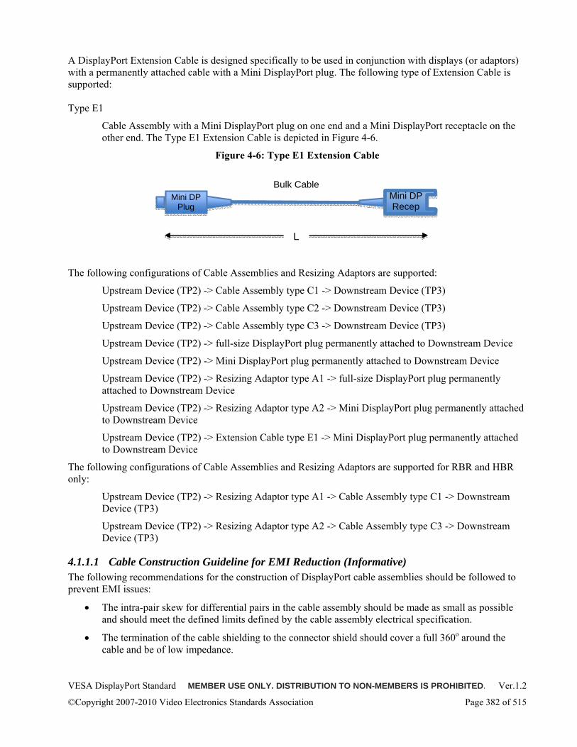
VESA DisplayPort Standard MEMBER USE ONLY. DISTRIBUTION TO NON-MEMBERS IS PROHIBITED. Ver.1.2
©Copyright 2007-2010 Video Electronics Standards Association Page 382 of 515
A DisplayPort Extension Cable is designed specifically to be used in conjunction with displays (or adaptors) with a permanently attached cable with a Mini DisplayPort plug. The following type of Extension Cable is supported: Type E1
Cable Assembly with a Mini DisplayPort plug on one end and a Mini DisplayPort receptacle on the other end. The Type E1 Extension Cable is depicted in Figure 4-6.
Figure 4-6: Type E1 Extension Cable
The following configurations of Cable Assemblies and Resizing Adaptors are supported:
Upstream Device (TP2) -> Cable Assembly type C1 -> Downstream Device (TP3)
Upstream Device (TP2) -> Cable Assembly type C2 -> Downstream Device (TP3)
Upstream Device (TP2) -> Cable Assembly type C3 -> Downstream Device (TP3)
Upstream Device (TP2) -> full-size DisplayPort plug permanently attached to Downstream Device
Upstream Device (TP2) -> Mini DisplayPort plug permanently attached to Downstream Device
Upstream Device (TP2) -> Resizing Adaptor type A1 -> full-size DisplayPort plug permanently attached to Downstream Device
Upstream Device (TP2) -> Resizing Adaptor type A2 -> Mini DisplayPort plug permanently attached to Downstream Device
Upstream Device (TP2) -> Extension Cable type E1 -> Mini DisplayPort plug permanently attached to Downstream Device
The following configurations of Cable Assemblies and Resizing Adaptors are supported for RBR and HBR only:
Upstream Device (TP2) -> Resizing Adaptor type A1 -> Cable Assembly type C1 -> Downstream Device (TP3)
Upstream Device (TP2) -> Resizing Adaptor type A2 -> Cable Assembly type C3 -> Downstream Device (TP3)
4.1.1.1 Cable Construction Guideline for EMI Reduction (Informative) The following recommendations for the construction of DisplayPort cable assemblies should be followed to prevent EMI issues:
• The intra-pair skew for differential pairs in the cable assembly should be made as small as possible and should meet the defined limits defined by the cable assembly electrical specification.
• The termination of the cable shielding to the connector shield should cover a full 360o around the cable and be of low impedance.
Bulk Cable
L
Mini DP Plug
Mini DP Recep
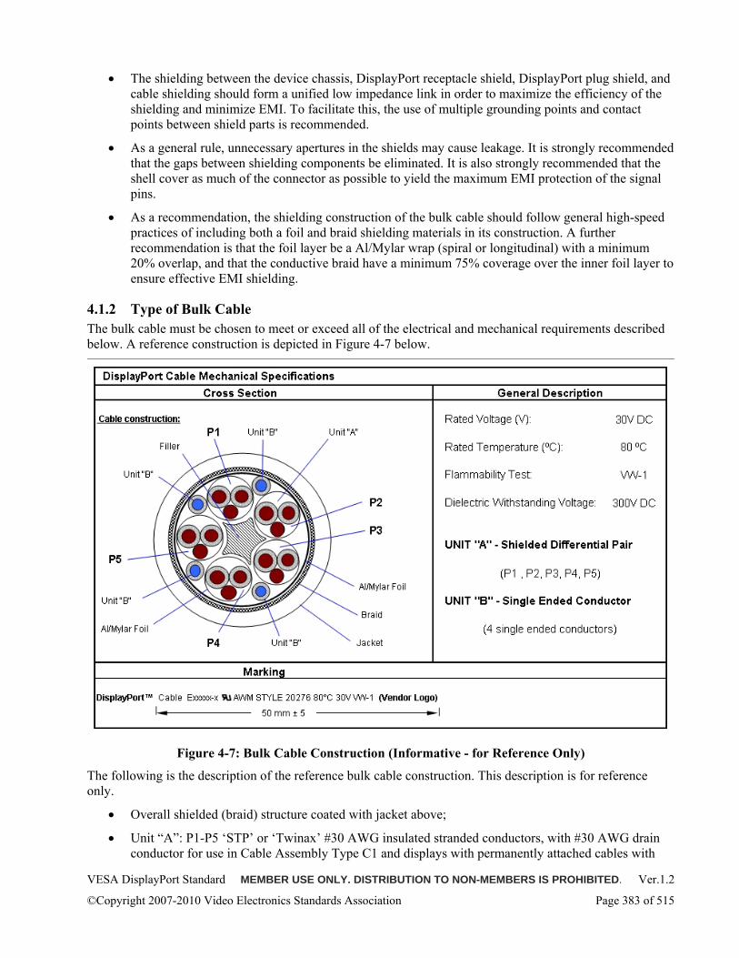
VESA DisplayPort Standard MEMBER USE ONLY. DISTRIBUTION TO NON-MEMBERS IS PROHIBITED. Ver.1.2
©Copyright 2007-2010 Video Electronics Standards Association Page 383 of 515
• The shielding between the device chassis, DisplayPort receptacle shield, DisplayPort plug shield, and cable shielding should form a unified low impedance link in order to maximize the efficiency of the shielding and minimize EMI. To facilitate this, the use of multiple grounding points and contact points between shield parts is recommended.
• As a general rule, unnecessary apertures in the shields may cause leakage. It is strongly recommended that the gaps between shielding components be eliminated. It is also strongly recommended that the shell cover as much of the connector as possible to yield the maximum EMI protection of the signal pins.
• As a recommendation, the shielding construction of the bulk cable should follow general high-speed practices of including both a foil and braid shielding materials in its construction. A further recommendation is that the foil layer be a Al/Mylar wrap (spiral or longitudinal) with a minimum 20% overlap, and that the conductive braid have a minimum 75% coverage over the inner foil layer to ensure effective EMI shielding.
4.1.2 Type of Bulk Cable The bulk cable must be chosen to meet or exceed all of the electrical and mechanical requirements described below. A reference construction is depicted in Figure 4-7 below.
Figure 4-7: Bulk Cable Construction (Informative - for Reference Only)
The following is the description of the reference bulk cable construction. This description is for reference only.
• Overall shielded (braid) structure coated with jacket above;
• Unit “A”: P1-P5 ‘STP’ or ‘Twinax’ #30 AWG insulated stranded conductors, with #30 AWG drain conductor for use in Cable Assembly Type C1 and displays with permanently attached cables with
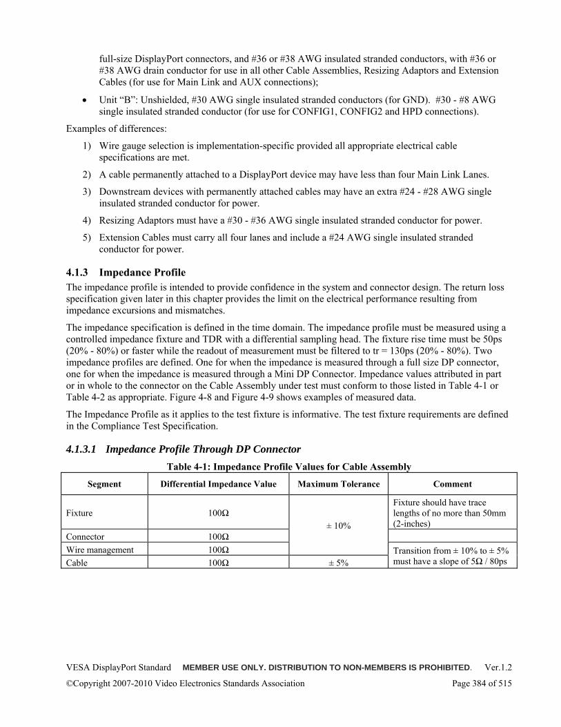
VESA DisplayPort Standard MEMBER USE ONLY. DISTRIBUTION TO NON-MEMBERS IS PROHIBITED. Ver.1.2
©Copyright 2007-2010 Video Electronics Standards Association Page 384 of 515
full-size DisplayPort connectors, and #36 or #38 AWG insulated stranded conductors, with #36 or #38 AWG drain conductor for use in all other Cable Assemblies, Resizing Adaptors and Extension Cables (for use for Main Link and AUX connections);
• Unit “B”: Unshielded, #30 AWG single insulated stranded conductors (for GND). #30 - #8 AWG single insulated stranded conductor (for use for CONFIG1, CONFIG2 and HPD connections).
Examples of differences:
1) Wire gauge selection is implementation-specific provided all appropriate electrical cable specifications are met.
2) A cable permanently attached to a DisplayPort device may have less than four Main Link Lanes.
3) Downstream devices with permanently attached cables may have an extra #24 - #28 AWG single insulated stranded conductor for power.
4) Resizing Adaptors must have a #30 - #36 AWG single insulated stranded conductor for power.
5) Extension Cables must carry all four lanes and include a #24 AWG single insulated stranded conductor for power.
4.1.3 Impedance Profile The impedance profile is intended to provide confidence in the system and connector design. The return loss specification given later in this chapter provides the limit on the electrical performance resulting from impedance excursions and mismatches.
The impedance specification is defined in the time domain. The impedance profile must be measured using a controlled impedance fixture and TDR with a differential sampling head. The fixture rise time must be 50ps (20% - 80%) or faster while the readout of measurement must be filtered to tr = 130ps (20% - 80%). Two impedance profiles are defined. One for when the impedance is measured through a full size DP connector, one for when the impedance is measured through a Mini DP Connector. Impedance values attributed in part or in whole to the connector on the Cable Assembly under test must conform to those listed in Table 4-1 or Table 4-2 as appropriate. Figure 4-8 and Figure 4-9 shows examples of measured data.
The Impedance Profile as it applies to the test fixture is informative. The test fixture requirements are defined in the Compliance Test Specification.
4.1.3.1 Impedance Profile Through DP Connector Table 4-1: Impedance Profile Values for Cable Assembly
Segment Differential Impedance Value Maximum Tolerance Comment
Fixture 100Ω Fixture should have trace lengths of no more than 50mm (2-inches)
Connector 100Ω Wire management 100Ω
± 10%
Cable 100Ω ± 5% Transition from ± 10% to ± 5% must have a slope of 5Ω / 80ps
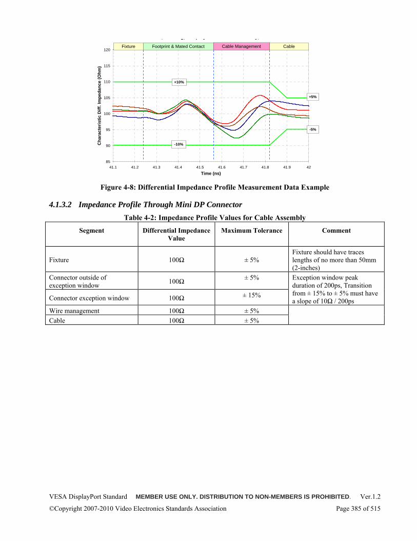
VESA DisplayPort Standard MEMBER USE ONLY. DISTRIBUTION TO NON-MEMBERS IS PROHIBITED. Ver.1.2
©Copyright 2007-2010 Video Electronics Standards Association Page 385 of 515
, g, p y y,
85
90
95
100
105
110
115
120
41.1 41.2 41.3 41.4 41.5 41.6 41.7 41.8 41.9 42
Time (ns)
Cha
ract
eris
tic D
iff. I
mpe
danc
e (O
hm)
Fixture Footprint & Mated Contact Cable Management Cable
-10%
+10%
-5%
+5%
Figure 4-8: Differential Impedance Profile Measurement Data Example
4.1.3.2 Impedance Profile Through Mini DP Connector Table 4-2: Impedance Profile Values for Cable Assembly
Segment Differential Impedance Value
Maximum Tolerance Comment
Fixture 100Ω ± 5% Fixture should have traces lengths of no more than 50mm (2-inches)
Connector outside of exception window 100Ω ± 5%
Connector exception window 100Ω ± 15%
Exception window peak duration of 200ps, Transition from ± 15% to ± 5% must have a slope of 10Ω / 200ps
Wire management 100Ω ± 5% Cable 100Ω ± 5%
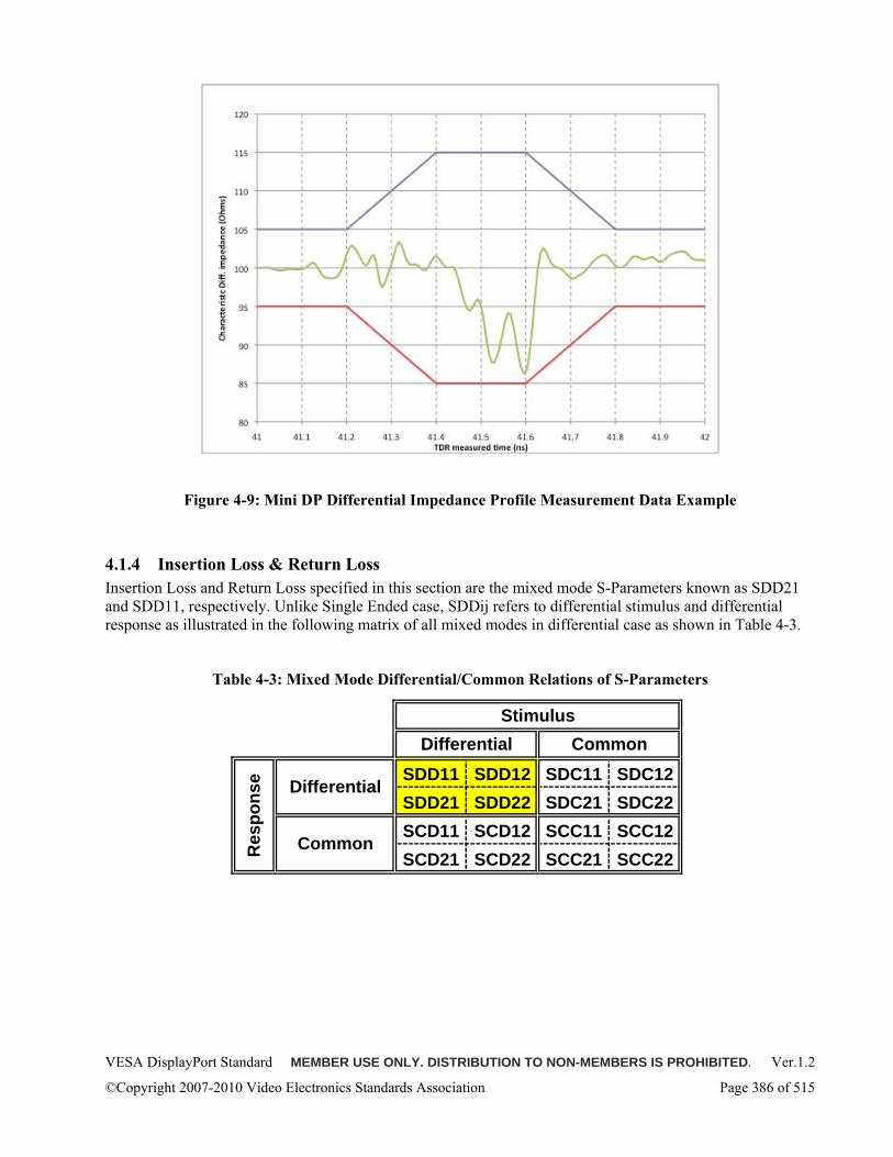
VESA DisplayPort Standard MEMBER USE ONLY. DISTRIBUTION TO NON-MEMBERS IS PROHIBITED. Ver.1.2
©Copyright 2007-2010 Video Electronics Standards Association Page 386 of 515
Figure 4-9: Mini DP Differential Impedance Profile Measurement Data Example
4.1.4 Insertion Loss & Return Loss Insertion Loss and Return Loss specified in this section are the mixed mode S-Parameters known as SDD21 and SDD11, respectively. Unlike Single Ended case, SDDij refers to differential stimulus and differential response as illustrated in the following matrix of all mixed modes in differential case as shown in Table 4-3.
Table 4-3: Mixed Mode Differential/Common Relations of S-Parameters
SDD11 SDD12 SDC11 SDC12SDD21 SDD22 SDC21 SDC22SCD11 SCD12 SCC11 SCC12SCD21 SCD22 SCC21 SCC22R
espo
nse
StimulusCommonDifferential
Differential
Common
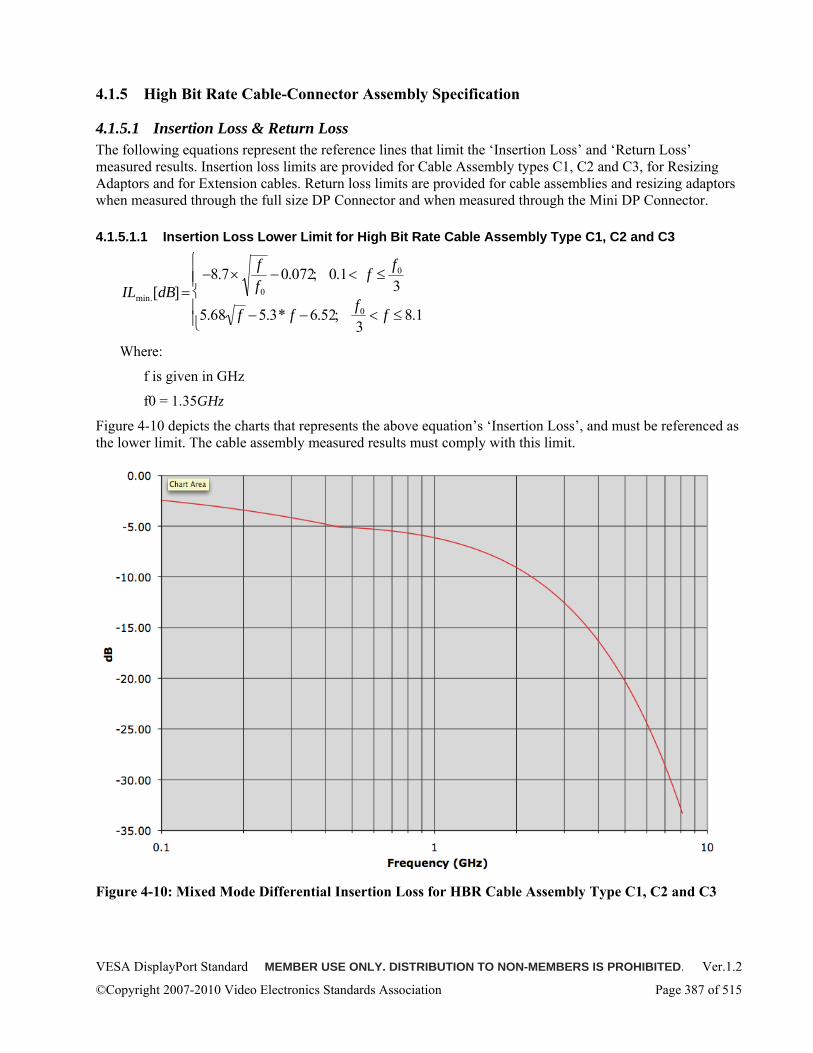
VESA DisplayPort Standard MEMBER USE ONLY. DISTRIBUTION TO NON-MEMBERS IS PROHIBITED. Ver.1.2
©Copyright 2007-2010 Video Electronics Standards Association Page 387 of 515
4.1.5 High Bit Rate Cable-Connector Assembly Specification
4.1.5.1 Insertion Loss & Return Loss The following equations represent the reference lines that limit the ‘Insertion Loss’ and ‘Return Loss’ measured results. Insertion loss limits are provided for Cable Assembly types C1, C2 and C3, for Resizing Adaptors and for Extension cables. Return loss limits are provided for cable assemblies and resizing adaptors when measured through the full size DP Connector and when measured through the Mini DP Connector.
4.1.5.1.1 Insertion Loss Lower Limit for High Bit Rate Cable Assembly Type C1, C2 and C3
ILmin.[dB] =−8.7×
ff0
−0.072; 0.1< f ≤f0
3
5.68 f −5.3* f −6.52; f0
3< f ≤ 8.1
⎧
⎨ ⎪ ⎪
⎩ ⎪ ⎪
Where:
f is given in GHz
f0 = 1.35GHz
Figure 4-10 depicts the charts that represents the above equation’s ‘Insertion Loss’, and must be referenced as the lower limit. The cable assembly measured results must comply with this limit.
Figure 4-10: Mixed Mode Differential Insertion Loss for HBR Cable Assembly Type C1, C2 and C3
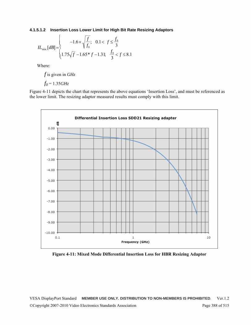
VESA DisplayPort Standard MEMBER USE ONLY. DISTRIBUTION TO NON-MEMBERS IS PROHIBITED. Ver.1.2
©Copyright 2007-2010 Video Electronics Standards Association Page 388 of 515
4.1.5.1.2 Insertion Loss Lower Limit for High Bit Rate Resizing Adaptors
ILmin.[dB] =−1.6 ×
ff0
; 0.1< f ≤f0
3
1.75 f −1.65* f −1.31;f0
3< f ≤ 8.1
⎧
⎨ ⎪ ⎪
⎩ ⎪ ⎪
Where:
f is given in GHz
f0 = 1.35GHz
Figure 4-11 depicts the chart that represents the above equations ‘Insertion Loss’, and must be referenced as the lower limit. The resizing adaptor measured results must comply with this limit.
Figure 4-11: Mixed Mode Differential Insertion Loss for HBR Resizing Adaptor
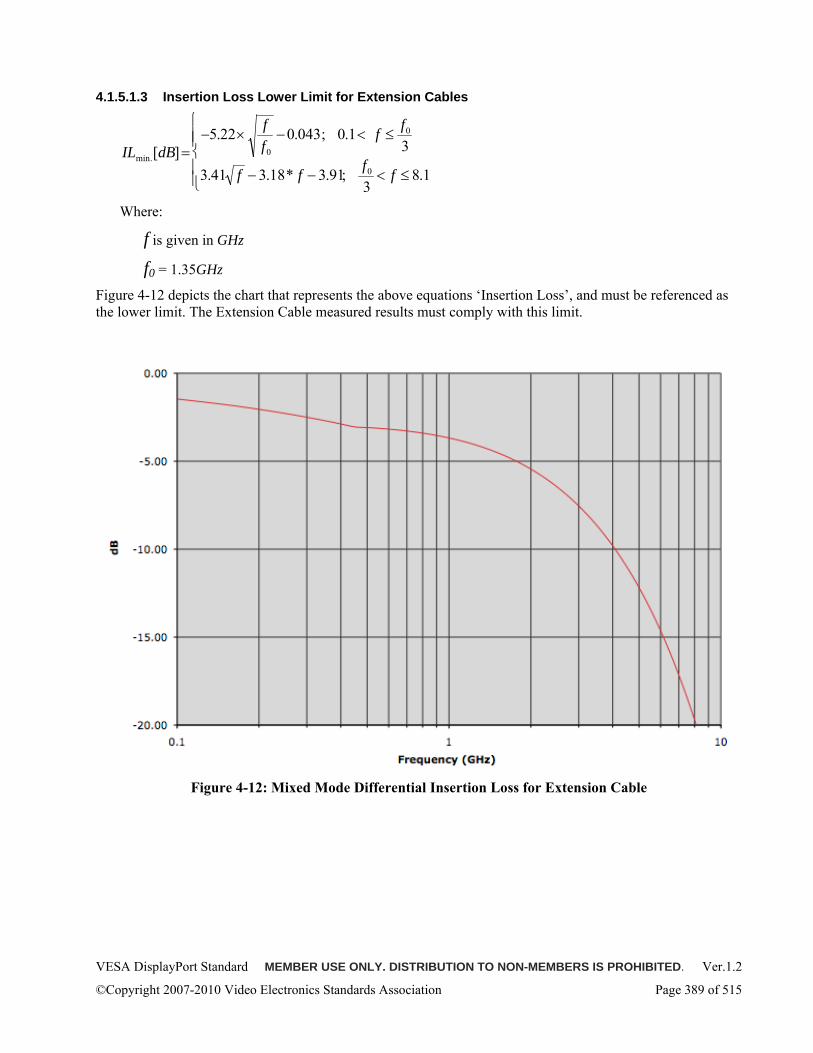
VESA DisplayPort Standard MEMBER USE ONLY. DISTRIBUTION TO NON-MEMBERS IS PROHIBITED. Ver.1.2
©Copyright 2007-2010 Video Electronics Standards Association Page 389 of 515
4.1.5.1.3 Insertion Loss Lower Limit for Extension Cables
ILmin.[dB] =−5.22×
ff0
−0.043; 0.1< f ≤f0
3
3.41 f − 3.18* f − 3.91; f0
3< f ≤ 8.1
⎧
⎨ ⎪ ⎪
⎩ ⎪ ⎪
Where:
f is given in GHz
f0 = 1.35GHz
Figure 4-12 depicts the chart that represents the above equations ‘Insertion Loss’, and must be referenced as the lower limit. The Extension Cable measured results must comply with this limit.
Figure 4-12: Mixed Mode Differential Insertion Loss for Extension Cable
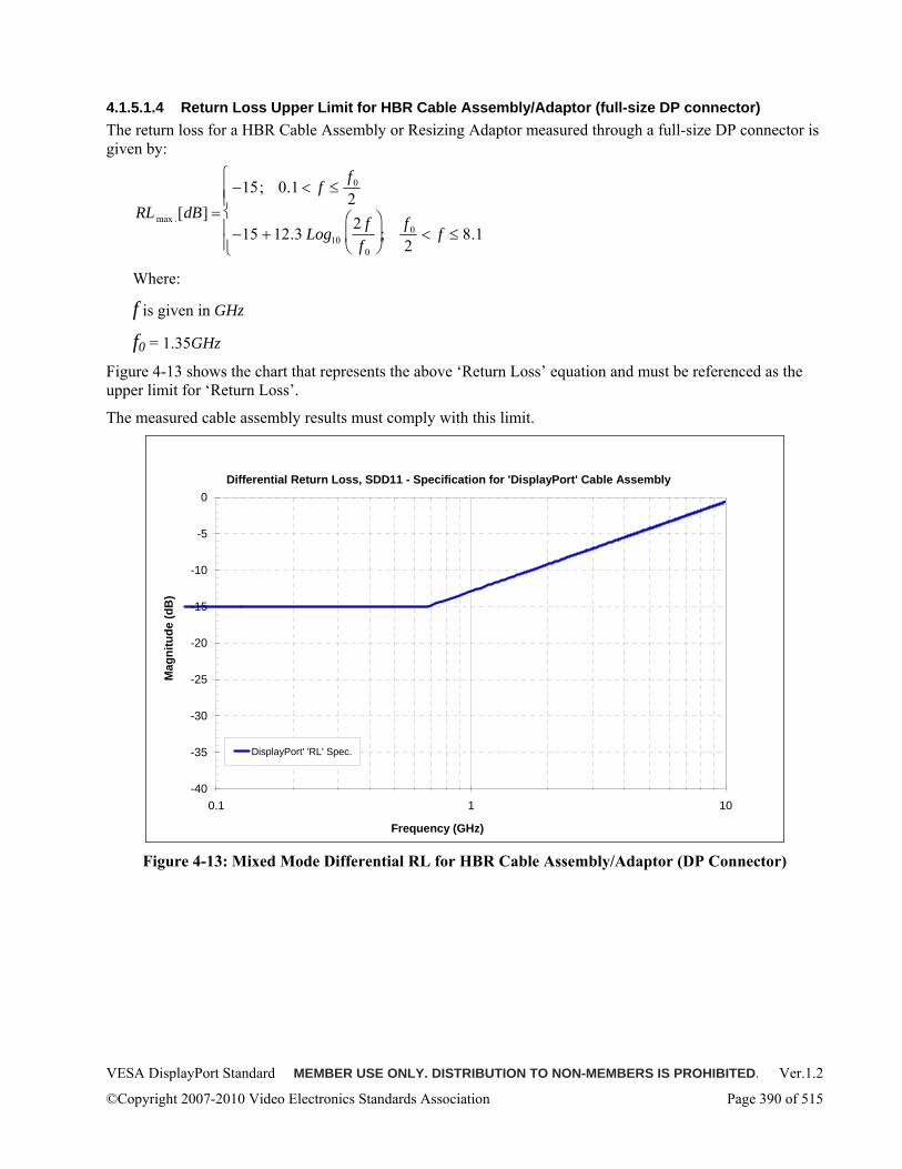
VESA DisplayPort Standard MEMBER USE ONLY. DISTRIBUTION TO NON-MEMBERS IS PROHIBITED. Ver.1.2
©Copyright 2007-2010 Video Electronics Standards Association Page 390 of 515
4.1.5.1.4 Return Loss Upper Limit for HBR Cable Assembly/Adaptor (full-size DP connector) The return loss for a HBR Cable Assembly or Resizing Adaptor measured through a full-size DP connector is given by:
RL max .[dB] =
−15; 0.1 < f ≤f0
2
−15 + 12.3 Log102 ff 0
⎛
⎝ ⎜
⎞
⎠ ⎟ ;
f 0
2< f ≤ 8.1
⎧
⎨ ⎪ ⎪
⎩ ⎪ ⎪
Where:
f is given in GHz
f0 = 1.35GHz
Figure 4-13 shows the chart that represents the above ‘Return Loss’ equation and must be referenced as the upper limit for ‘Return Loss’.
The measured cable assembly results must comply with this limit.
Differential Return Loss, SDD11 - Specification for 'DisplayPort' Cable Assembly
-40
-35
-30
-25
-20
-15
-10
-5
0
0.1 1 10
Frequency (GHz)
Mag
nitu
de (d
B)
DisplayPort' 'RL' Spec.
Figure 4-13: Mixed Mode Differential RL for HBR Cable Assembly/Adaptor (DP Connector)
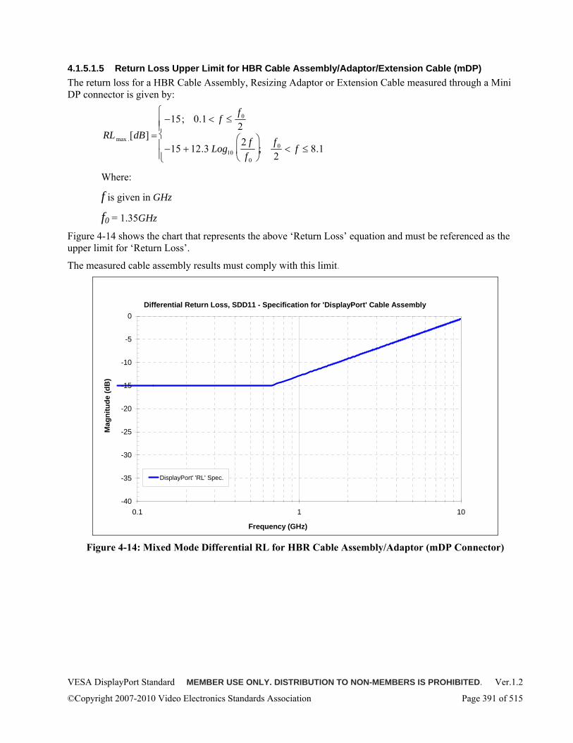
VESA DisplayPort Standard MEMBER USE ONLY. DISTRIBUTION TO NON-MEMBERS IS PROHIBITED. Ver.1.2
©Copyright 2007-2010 Video Electronics Standards Association Page 391 of 515
4.1.5.1.5 Return Loss Upper Limit for HBR Cable Assembly/Adaptor/Extension Cable (mDP) The return loss for a HBR Cable Assembly, Resizing Adaptor or Extension Cable measured through a Mini DP connector is given by:
RL max .[dB] =
−15; 0.1 < f ≤f0
2
−15 + 12.3 Log102 ff 0
⎛
⎝ ⎜
⎞
⎠ ⎟ ;
f 0
2< f ≤ 8.1
⎧
⎨ ⎪ ⎪
⎩ ⎪ ⎪
Where:
f is given in GHz
f0 = 1.35GHz
Figure 4-14 shows the chart that represents the above ‘Return Loss’ equation and must be referenced as the upper limit for ‘Return Loss’.
The measured cable assembly results must comply with this limit.
Differential Return Loss, SDD11 - Specification for 'DisplayPort' Cable Assembly
-40
-35
-30
-25
-20
-15
-10
-5
0
0.1 1 10
Frequency (GHz)
Mag
nitu
de (d
B)
DisplayPort' 'RL' Spec.
Figure 4-14: Mixed Mode Differential RL for HBR Cable Assembly/Adaptor (mDP Connector)
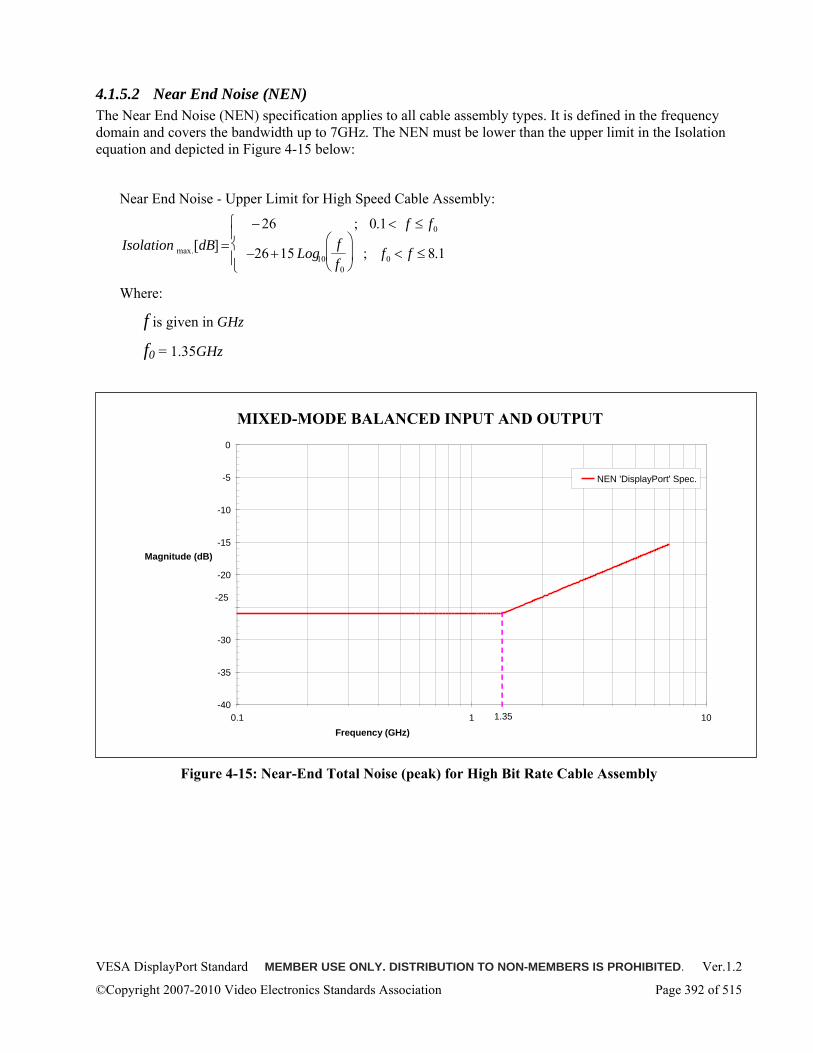
VESA DisplayPort Standard MEMBER USE ONLY. DISTRIBUTION TO NON-MEMBERS IS PROHIBITED. Ver.1.2
©Copyright 2007-2010 Video Electronics Standards Association Page 392 of 515
4.1.5.2 Near End Noise (NEN) The Near End Noise (NEN) specification applies to all cable assembly types. It is defined in the frequency domain and covers the bandwidth up to 7GHz. The NEN must be lower than the upper limit in the Isolation equation and depicted in Figure 4-15 below:
Near End Noise - Upper Limit for High Speed Cable Assembly:
Isolation max.[dB] =−26 ; 0.1 < f ≤ f0
−26 +15 Log10ff0
⎛
⎝ ⎜
⎞
⎠ ⎟ ; f0 < f ≤ 8.1
⎧ ⎨ ⎪
⎩ ⎪
Where:
f is given in GHz
f0 = 1.35GHz
Figure 4-15: Near-End Total Noise (peak) for High Bit Rate Cable Assembly
MIXED-MODE BALANCED INPUT AND OUTPUT:
-40
-35
-30
-20
-15
-10
-5
0
0.1 1 10Frequency (GHz)
Magnitude (dB)
NEN 'DisplayPort' Spec.
1.35
-25
MIXED-MODE BALANCED INPUT AND OUTPUT
VESA DisplayPort Standard MEMBER USE ONLY. DISTRIBUTION TO NON-MEMBERS IS PROHIBITED. Ver.1.2
©Copyright 2007-2010 Video Electronics Standards Association Page 393 of 515
4.1.5.3 Power Sum Equal Level Far-End Noise (PSELFEN) The Power Sum Equal Level Far-End Noise (PSELFEN) specification applies to all cable assembly types. The PSELFEN represents the difference between cable insertion loss and the total power sum far end noise from aggressor cable lanes.
∑⎟⎠⎞
⎜⎝⎛
×=n fFENn
fPSFEN1
10)(
10log10)(
( ) ( ) ( )fILfPSFENfPSELFEN −=
Where:
FENn(f) is the far-end noise in dB
IL(f) is the victim lane insertion loss in dB
The Power Sum Equal Level Far-End Noise must be lower than the upper limit as depicted in Figure 4-16 below.
Power Sum Equal Level Far-End Noise - Upper Limit for High Speed Cable Assembly:
PSELFEN max.[dB] =−22+ 6Log10
ff0
⎛
⎝ ⎜
⎞
⎠ ⎟ ; 0.1< f ≤ f0
−22+ 40Log10ff0
⎛
⎝ ⎜
⎞
⎠ ⎟ ; f0 < f ≤ 8.1
⎧
⎨ ⎪ ⎪
⎩ ⎪ ⎪
Where:
f is given in GHz
f0 = 2.7GHz
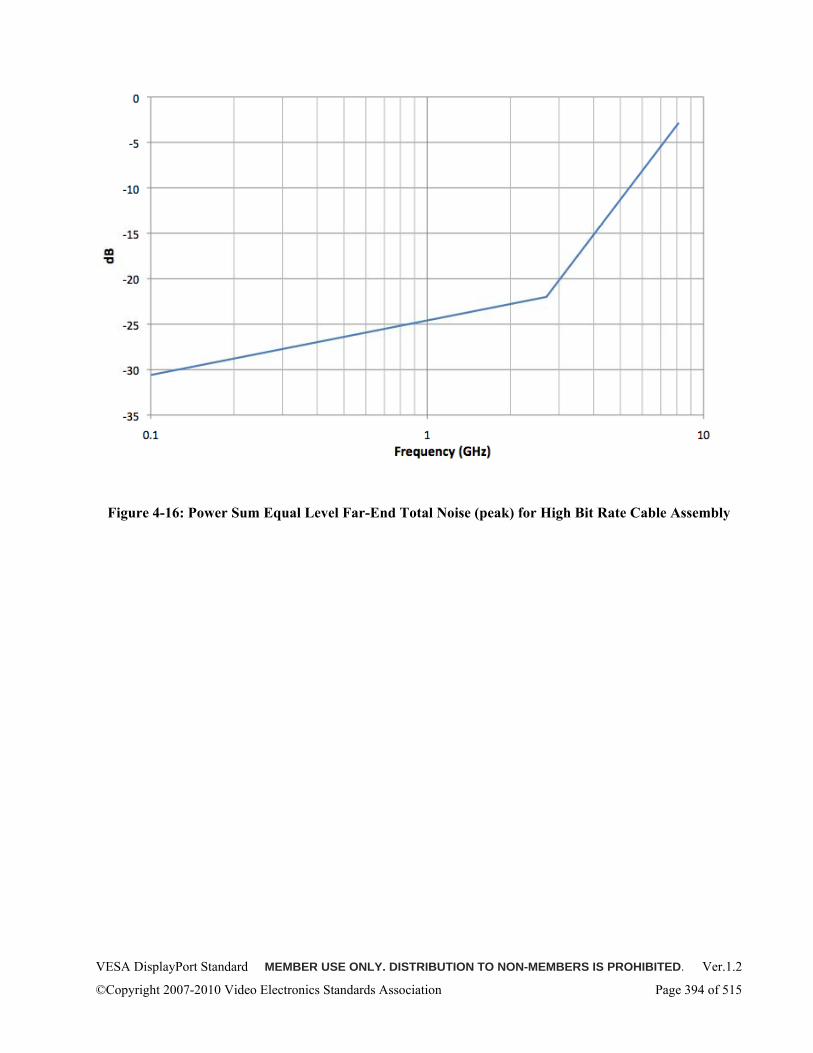
VESA DisplayPort Standard MEMBER USE ONLY. DISTRIBUTION TO NON-MEMBERS IS PROHIBITED. Ver.1.2
©Copyright 2007-2010 Video Electronics Standards Association Page 394 of 515
Figure 4-16: Power Sum Equal Level Far-End Total Noise (peak) for High Bit Rate Cable Assembly
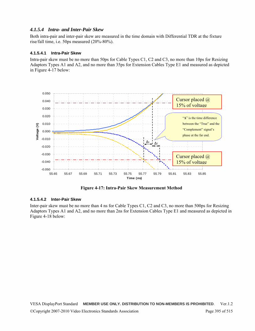
VESA DisplayPort Standard MEMBER USE ONLY. DISTRIBUTION TO NON-MEMBERS IS PROHIBITED. Ver.1.2
©Copyright 2007-2010 Video Electronics Standards Association Page 395 of 515
4.1.5.4 Intra- and Inter-Pair Skew Both intra-pair and inter-pair skew are measured in the time domain with Differential TDR at the fixture rise/fall time, i.e. 50ps measured (20%-80%).
4.1.5.4.1 Intra-Pair Skew Intra-pair skew must be no more than 50ps for Cable Types C1, C2 and C3, no more than 10ps for Resizing Adaptors Types A1 and A2, and no more than 35ps for Extension Cables Type E1 and measured as depicted in Figure 4-17 below:
Differerntial Intra-pair Skew Measurement, Cable Assembly, AWG#30, STP, 3m long
-0.050
-0.040
-0.030
-0.020
-0.010
0.000
0.010
0.020
0.030
0.040
0.050
55.65 55.67 55.69 55.71 55.73 55.75 55.77 55.79 55.81 55.83 55.85Time (ns)
Vol
tage
(V
)
Δ1 Δ2
Cursor placed @ 15% of voltage
Cursor placed @ 15% of voltage
“Δ” is the time difference
between the “True” and the
“Complement” signal’s
phase at the far end.
Figure 4-17: Intra-Pair Skew Measurement Method
4.1.5.4.2 Inter-Pair Skew Inter-pair skew must be no more than 4 ns for Cable Types C1, C2 and C3, no more than 500ps for Resizing Adaptors Types A1 and A2, and no more than 2ns for Extension Cables Type E1 and measured as depicted in Figure 4-18 below:
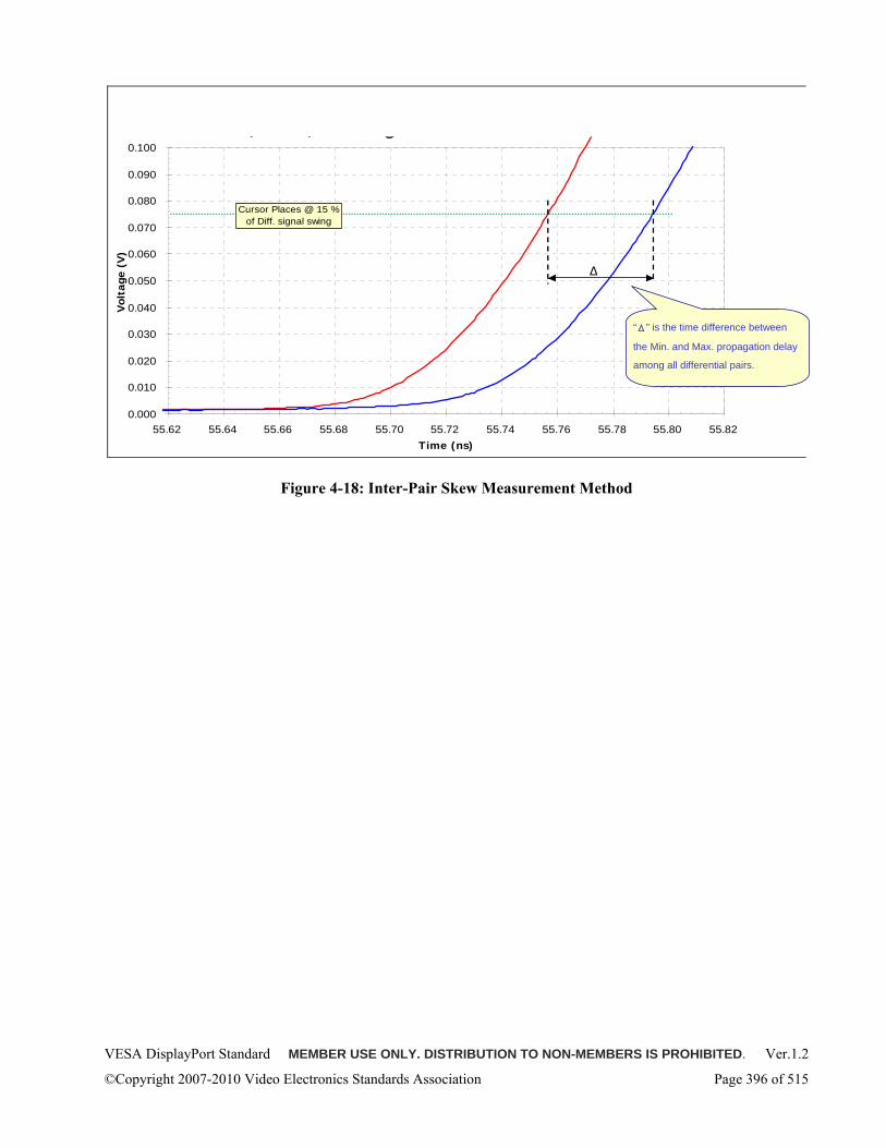
VESA DisplayPort Standard MEMBER USE ONLY. DISTRIBUTION TO NON-MEMBERS IS PROHIBITED. Ver.1.2
©Copyright 2007-2010 Video Electronics Standards Association Page 396 of 515
Cable Assembly, Inter-pair Skew MeasurementAWG#30, 'STP', 3m long
0.000
0.010
0.020
0.030
0.040
0.050
0.060
0.070
0.080
0.090
0.100
55.62 55.64 55.66 55.68 55.70 55.72 55.74 55.76 55.78 55.80 55.82Time (ns)
Vol
tage
(V
)
Cursor Places @ 15 %of Diff. signal swing
Δ
Figure 4-18: Inter-Pair Skew Measurement Method
“Δ” is the time difference between
the Min. and Max. propagation delay
among all differential pairs.
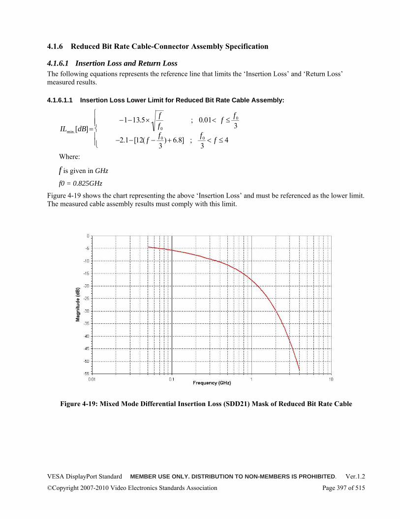
VESA DisplayPort Standard MEMBER USE ONLY. DISTRIBUTION TO NON-MEMBERS IS PROHIBITED. Ver.1.2
©Copyright 2007-2010 Video Electronics Standards Association Page 397 of 515
4.1.6 Reduced Bit Rate Cable-Connector Assembly Specification
4.1.6.1 Insertion Loss and Return Loss The following equations represents the reference line that limits the ‘Insertion Loss’ and ‘Return Loss’ measured results.
4.1.6.1.1 Insertion Loss Lower Limit for Reduced Bit Rate Cable Assembly:
ILmin.[dB] =−1−13.5×
ff0
; 0.01< f ≤f0
3
−2.1−[12( f −f0
3) + 6.8] ; f0
3< f ≤ 4
⎧
⎨ ⎪ ⎪
⎩ ⎪ ⎪
Where:
f is given in GHz
f0 = 0.825GHz
Figure 4-19 shows the chart representing the above ‘Insertion Loss’ and must be referenced as the lower limit. The measured cable assembly results must comply with this limit.
Figure 4-19: Mixed Mode Differential Insertion Loss (SDD21) Mask of Reduced Bit Rate Cable
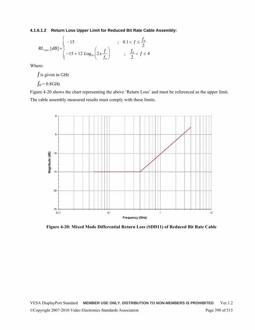
VESA DisplayPort Standard MEMBER USE ONLY. DISTRIBUTION TO NON-MEMBERS IS PROHIBITED. Ver.1.2
©Copyright 2007-2010 Video Electronics Standards Association Page 398 of 515
4.1.6.1.2 Return Loss Upper Limit for Reduced Bit Rate Cable Assembly:
RLmax .[dB] =−15 ; 0.1 < f ≤
f0
2
−15 + 12 Log10 2x ff0
⎛
⎝ ⎜
⎞
⎠ ⎟ ; f0
2< f ≤ 4
⎧
⎨ ⎪ ⎪
⎩ ⎪ ⎪
Where:
f is given in GHz
f0 = 0.8GHz
Figure 4-20 shows the chart representing the above ‘Return Loss’ and must be referenced as the upper limit.
The cable assembly measured results must comply with these limits.
Figure 4-20: Mixed Mode Differential Return Loss (SDD11) of Reduced Bit Rate Cable
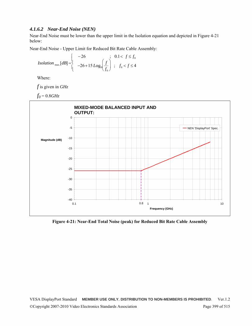
VESA DisplayPort Standard MEMBER USE ONLY. DISTRIBUTION TO NON-MEMBERS IS PROHIBITED. Ver.1.2
©Copyright 2007-2010 Video Electronics Standards Association Page 399 of 515
4.1.6.2 Near-End Noise (NEN) Near-End Noise must be lower than the upper limit in the Isolation equation and depicted in Figure 4-21 below:
Near-End Noise - Upper Limit for Reduced Bit Rate Cable Assembly:
Isolation max.[dB] =−26 ; 0.1 < f ≤ f0
−26 +15 Log10ff0
⎛
⎝ ⎜
⎞
⎠ ⎟ ; f0 < f ≤ 4
⎧ ⎨ ⎪
⎩ ⎪
Where:
f is given in GHz
f0 = 0.8GHz
Figure 4-21: Near-End Total Noise (peak) for Reduced Bit Rate Cable Assembly
MIXED-MODE BALANCED INPUT AND OUTPUT:
-40
-35
-30
-25
-20
-15
-10
-5
0
0.1 1 10
Frequency (GHz)
Magnitude (dB)
NEN 'DisplayPort' Spec.
0.8
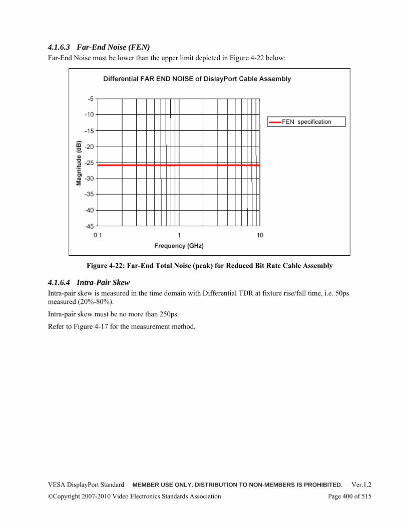
VESA DisplayPort Standard MEMBER USE ONLY. DISTRIBUTION TO NON-MEMBERS IS PROHIBITED. Ver.1.2
©Copyright 2007-2010 Video Electronics Standards Association Page 400 of 515
4.1.6.3 Far-End Noise (FEN) Far-End Noise must be lower than the upper limit depicted in Figure 4-22 below:
Figure 4-22: Far-End Total Noise (peak) for Reduced Bit Rate Cable Assembly
4.1.6.4 Intra-Pair Skew Intra-pair skew is measured in the time domain with Differential TDR at fixture rise/fall time, i.e. 50ps measured (20%-80%).
Intra-pair skew must be no more than 250ps.
Refer to Figure 4-17 for the measurement method.
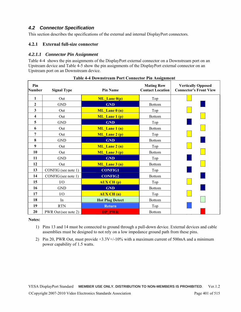
VESA DisplayPort Standard MEMBER USE ONLY. DISTRIBUTION TO NON-MEMBERS IS PROHIBITED. Ver.1.2
©Copyright 2007-2010 Video Electronics Standards Association Page 401 of 515
4.2 Connector Specification This section describes the specifications of the external and internal DisplayPort connectors.
4.2.1 External full-size connector
4.2.1.1 Connector Pin Assignment Table 4-4 shows the pin assignments of the DisplayPort external connector on a Downstream port on an Upstream device and Table 4-5 show the pin assignments of the DisplayPort external connector on an Upstream port on an Downstream device.
Table 4-4 Downstream Port Connector Pin Assignment
Pin Number Signal Type Pin Name
Mating Row Contact Location
Vertically Opposed Connector’s Front View
1 Out ML_Lane 0(p) Top 2 GND GND Bottom 3 Out ML_Lane 0 (n) Top 4 Out ML_Lane 1 (p) Bottom 5 GND GND Top 6 Out ML_Lane 1 (n) Bottom 7 Out ML_Lane 2 (p) Top 8 GND GND Bottom 9 Out ML_Lane 2 (n) Top
10 Out ML_Lane 3 (p) Bottom 11 GND GND Top 12 Out ML_Lane 3 (n) Bottom 13 CONFIG (see note 1) CONFIG1 Top 14 CONFIG (see note 1) CONFIG2 Bottom 15 I/O AUX CH (p) Top 16 GND GND Bottom 17 I/O AUX CH (n) Top 18 In Hot Plug Detect Bottom 19 RTN Return Top 20 PWR Out (see note 2) DP_PWR Bottom
Notes:
1) Pins 13 and 14 must be connected to ground through a pull-down device. External devices and cable assemblies must be designed to not rely on a low impedance ground path from these pins.
2) Pin 20, PWR Out, must provide +3.3V+/-10% with a maximum current of 500mA and a minimum power capability of 1.5 watts.
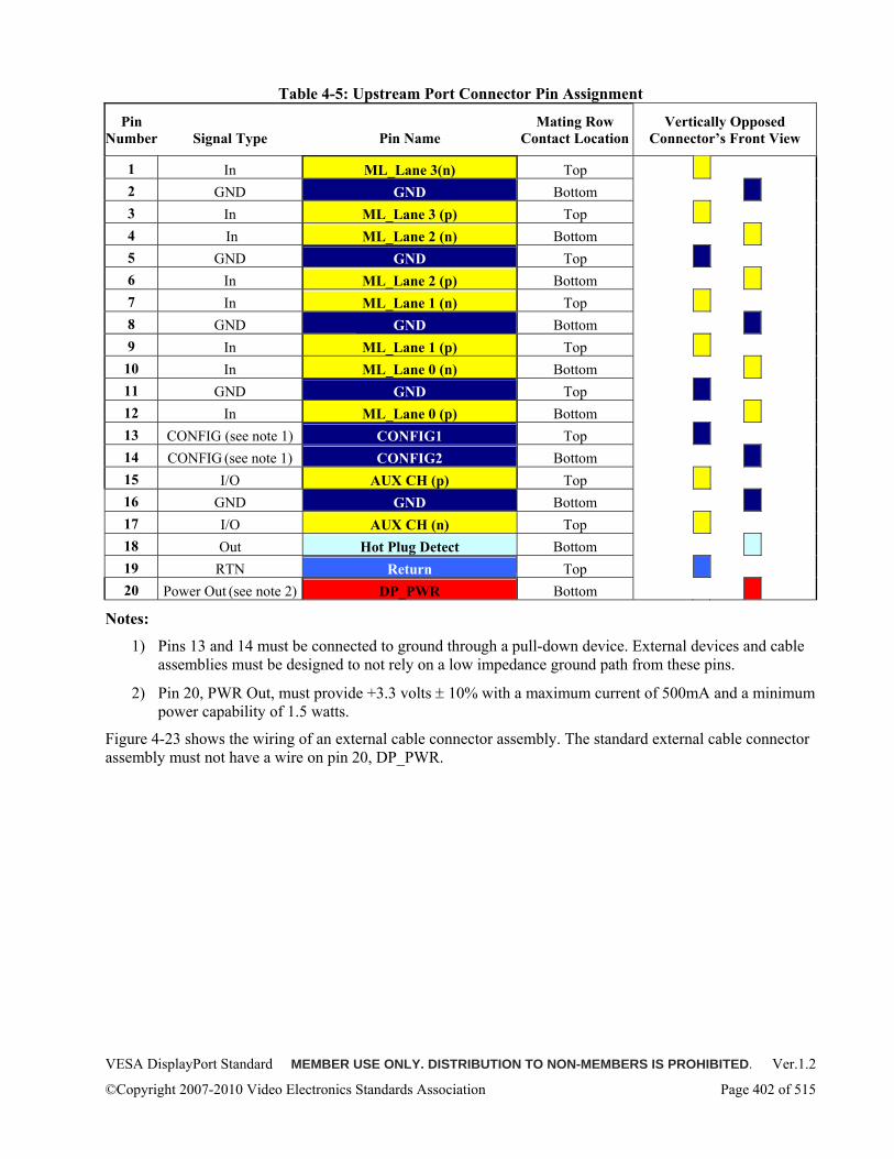
VESA DisplayPort Standard MEMBER USE ONLY. DISTRIBUTION TO NON-MEMBERS IS PROHIBITED. Ver.1.2
©Copyright 2007-2010 Video Electronics Standards Association Page 402 of 515
Table 4-5: Upstream Port Connector Pin Assignment
Pin Number Signal Type Pin Name
Mating Row Contact Location
Vertically Opposed Connector’s Front View
1 In ML_Lane 3(n) Top 2 GND GND Bottom 3 In ML_Lane 3 (p) Top 4 In ML_Lane 2 (n) Bottom 5 GND GND Top 6 In ML_Lane 2 (p) Bottom 7 In ML_Lane 1 (n) Top 8 GND GND Bottom 9 In ML_Lane 1 (p) Top
10 In ML_Lane 0 (n) Bottom 11 GND GND Top 12 In ML_Lane 0 (p) Bottom 13 CONFIG (see note 1) CONFIG1 Top 14 CONFIG (see note 1) CONFIG2 Bottom 15 I/O AUX CH (p) Top 16 GND GND Bottom 17 I/O AUX CH (n) Top 18 Out Hot Plug Detect Bottom 19 RTN Return Top 20 Power Out (see note 2) DP_PWR Bottom
Notes:
1) Pins 13 and 14 must be connected to ground through a pull-down device. External devices and cable assemblies must be designed to not rely on a low impedance ground path from these pins.
2) Pin 20, PWR Out, must provide +3.3 volts ± 10% with a maximum current of 500mA and a minimum power capability of 1.5 watts.
Figure 4-23 shows the wiring of an external cable connector assembly. The standard external cable connector assembly must not have a wire on pin 20, DP_PWR.
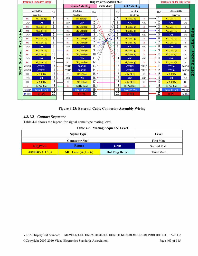
VESA DisplayPort Standard MEMBER USE ONLY. DISTRIBUTION TO NON-MEMBERS IS PROHIBITED. Ver.1.2
©Copyright 2007-2010 Video Electronics Standards Association Page 403 of 515
Figure 4-23: External Cable Connector Assembly Wiring
4.2.1.2 Contact Sequence Table 4-6 shows the legend for signal name/type mating level.
Table 4-6: Mating Sequence Level
Signal Type Level
Connector Shell First Mate DP_PWR Return GND Second Mate
Auxiliary (+) / (-) ML_Lane (i) (+) / (-) Hot Plug Detect Third Mate
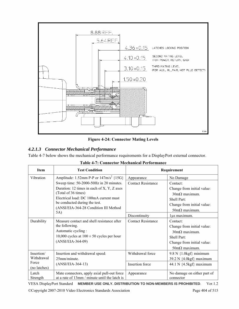
VESA DisplayPort Standard MEMBER USE ONLY. DISTRIBUTION TO NON-MEMBERS IS PROHIBITED. Ver.1.2
©Copyright 2007-2010 Video Electronics Standards Association Page 404 of 515
Figure 4-24: Connector Mating Levels
4.2.1.3 Connector Mechanical Performance Table 4-7 below shows the mechanical performance requirements for a DisplayPort external connector.
Table 4-7: Connector Mechanical Performance
Item Test Condition Requirement
Appearance No Damage Contact Resistance Contact:
Change from initial value: 30mΩ maximum.
Shell Part: Change from initial value:
50mΩ maximum.
Vibration Amplitude: 1.52mm P-P or 147m/s2 15G Sweep time: 50-2000-50Hz in 20 minutes. Duration: 12 times in each of X, Y, Z axes (Total of 36 times) Electrical load: DC 100mA current must be conducted during the test. (ANSI/EIA-364-28 Condition III Method 5A)
Discontinuity 1µs maximum. Durability Measure contact and shell resistance after
the following. Automatic cycling : 10,000 cycles at 100 ± 50 cycles per hour (ANSI/EIA-364-09)
Contact Resistance Contact: Change from initial value:
30mΩ maximum. Shell Part: Change from initial value:
50mΩ maximum. Withdrawal force 9.8 N 1.0kgf minimum
39.2 N 4.0kgf maximum Insertion/ Withdrawal Force (no latches)
Insertion and withdrawal speed: 25mm/minute. (ANSI/EIA-364-13) Insertion force 44.1 N 4.5kgf maximum
Latch Strength
Mate connectors, apply axial pull-out force at a rate of 13mm / minute until the latch is
Appearance No damage on either part of connector
VESA DisplayPort Standard MEMBER USE ONLY. DISTRIBUTION TO NON-MEMBERS IS PROHIBITED. Ver.1.2
©Copyright 2007-2010 Video Electronics Standards Association Page 405 of 515
Item Test Condition Requirement
disengaged or damaged. (ANSI/EIA-364-98)
Pull force 49.0 N 5.0kgf minimum
Discontinuity 1µs maximum. Cable Flex 100 cycles in each of 2 planes. Dimension: X = 3.7 x Cable Diameter. (ANSI/EIA-364-41, Condition I)
Dielectric Withstanding Voltage and Insulation Resistance.
Conform to item of dielectric withstanding voltage and insulation resistance
4.2.1.4 Connector Electrical Performance Table 4-8 below shows the electrical performance requirements for a DisplayPort external connector.
Table 4-8: Connector Electrical Performance
Item Test Condition Requirement
Low Level Contact Resistance
Mated connectors, Contact: measured by dry circuit, 20mVolts maximum, and 10mA. Shell: measured by open circuit, 5 Volts maximum, 100mA. (ANSI/EIA-364-23)
Contact: Change from initial value = 30mΩ maximum Shell: Change from initial value = 50mΩ maximum
Dielectric Strength
Unmated connectors, apply 500 Volts RMS between adjacent terminal and ground. (ANSI/EIA 364-20,Method 301) Mated connector, apply 300 Volts RMS between adjacent terminal and ground.
No Breakdown
Unmated connectors, apply 500 Volts DC between adjacent terminal and ground. (ANSI/EIA 364-21,Method 302)
Unmated: 100MΩ minimum Insulation Resistance
Mated connectors, apply 150 Volts DC between adjacent terminal and ground.
Mated: 10MΩ minimum
Contact Current Rating
55 °C, maximum ambient 85 °C, maximum temperature change (ANSI/EIA-364-70,TP-70)
0.5A minimum
Applied Voltage Rating
40 Volts RMS continuous maximum, on any signal pin with respect to the shield.
No Breakdown
Electrostatic Discharge
Test unmated connectors from 1kVolt to 8kVolts in 1kVolt steps using 8mm ball probe. (IEC61000-4-2)
No evidence of discharge to contacts at 8kVolts
VESA DisplayPort Standard MEMBER USE ONLY. DISTRIBUTION TO NON-MEMBERS IS PROHIBITED. Ver.1.2
©Copyright 2007-2010 Video Electronics Standards Association Page 406 of 515
4.2.1.5 Connector Environment Performance Table 4-9 below shows the environment performance requirements for a DisplayPort external connector.
Table 4-9: Connector Environment Performance
Item Test Condition Requirement
Appearance No Damage Thermal Shock
10 cycles of: a) -55°C for 30 minutes b) +85°C for 30 minutes (ANSI/EIA-364-32, Condition I)
Contact Resistance
Contact: Change from initial value:
30mΩ maximum. Shell Part: Change from initial value:
50mΩ maximum. Appearance No Damage A) Mate connectors together and perform the test as
follows: Temperature : +25 to +85°C Relative Humidity : 80 to 95% Duration : Four cycles (96 hours)
Upon completion of the test, specimens must be conditioned at ambient room conditions for 24 hours, after which the specified measurements must be performed. (ANSI/EIA-364-31)
Contact Resistance
Contact: Change from initial value:
30mΩ maximum. Shell Part: Change from initial value:
50mΩ maximum.
Appearance No Damage
Humidity
B) Unmate connectors and perform the test as follows:
Temperature : +25 to +85°C Relative Humidity : 80 to 95% Duration : Four cycles (96 hours)
Upon completion of the test, specimens must be conditioned at ambient room conditions for 24 hours, after which the specified measurements must be performed. (ANSI/EIA-364-31)
Dielectric Withstanding Voltage and Insulation Resistance
Conform to item of Dielectric Withstanding Voltage and Insulation Resistance
Appearance No Damage Thermal Aging
Mate connectors and expose to (+105 ± 2)°C for 250 hours. Upon completion of the exposure period, the test specimens must be conditioned at ambient room conditions for one to two hours after which the specified measurements must be performed. (ANSI/EIA-364-17, Condition 4, Method A)
Contact Resistance
Contact: Change from initial value:
30mΩ maximum. Shell Part: Change from initial value:
50mΩ maximum.
4.2.1.6 Connector Performance Test Sequence To evaluate the connector performance, the test sequence must follow the test groups 1, 2, 3 and 7 in the ANSI/EIA Standard (EIA-364-1000.01).
4.2.1.7 Connector Drawings (Per Molex Connector P/N: 47272-0002) Figure 4-25 below shows the DisplayPort external connector. All dimensions are in mm.
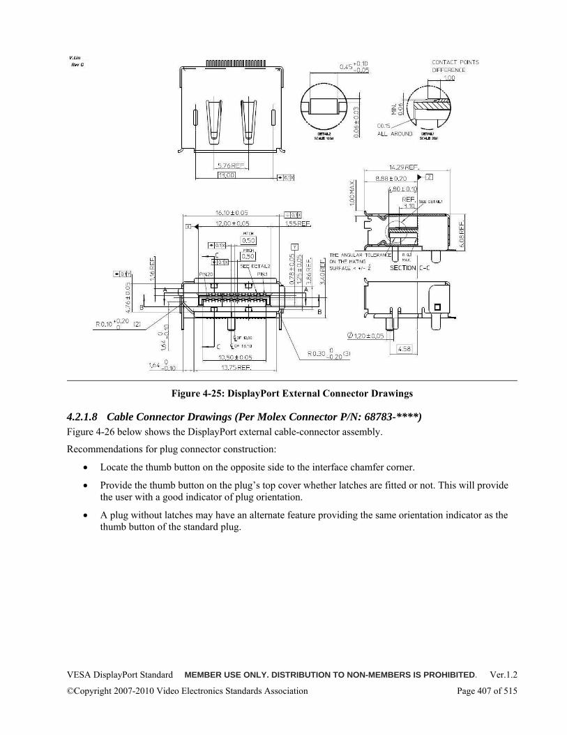
VESA DisplayPort Standard MEMBER USE ONLY. DISTRIBUTION TO NON-MEMBERS IS PROHIBITED. Ver.1.2
©Copyright 2007-2010 Video Electronics Standards Association Page 407 of 515
Figure 4-25: DisplayPort External Connector Drawings
4.2.1.8 Cable Connector Drawings (Per Molex Connector P/N: 68783-****) Figure 4-26 below shows the DisplayPort external cable-connector assembly.
Recommendations for plug connector construction:
• Locate the thumb button on the opposite side to the interface chamfer corner.
• Provide the thumb button on the plug’s top cover whether latches are fitted or not. This will provide the user with a good indicator of plug orientation.
• A plug without latches may have an alternate feature providing the same orientation indicator as the thumb button of the standard plug.
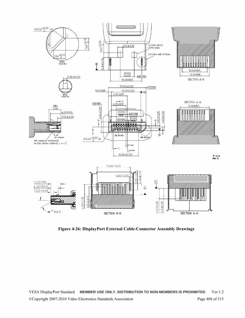
VESA DisplayPort Standard MEMBER USE ONLY. DISTRIBUTION TO NON-MEMBERS IS PROHIBITED. Ver.1.2
©Copyright 2007-2010 Video Electronics Standards Association Page 408 of 515
Figure 4-26: DisplayPort External Cable-Connector Assembly Drawings
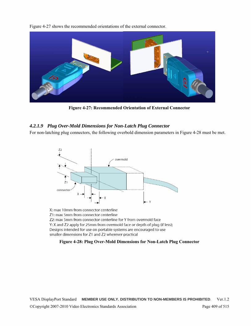
VESA DisplayPort Standard MEMBER USE ONLY. DISTRIBUTION TO NON-MEMBERS IS PROHIBITED. Ver.1.2
©Copyright 2007-2010 Video Electronics Standards Association Page 409 of 515
Figure 4-27 shows the recommended orientations of the external connector.
Figure 4-27: Recommended Orientation of External Connector
4.2.1.9 Plug Over-Mold Dimensions for Non-Latch Plug Connector For non-latching plug connectors, the following overbold dimension parameters in Figure 4-28 must be met.
Figure 4-28: Plug Over-Mold Dimensions for Non-Latch Plug Connector
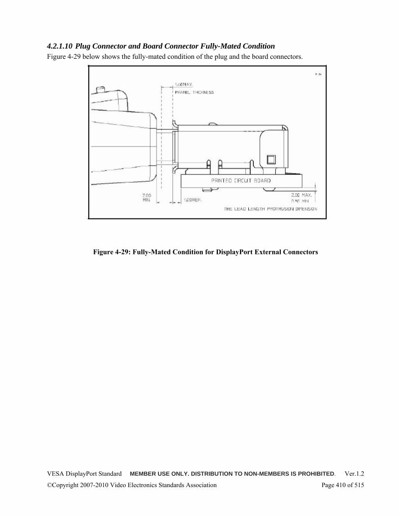
VESA DisplayPort Standard MEMBER USE ONLY. DISTRIBUTION TO NON-MEMBERS IS PROHIBITED. Ver.1.2
©Copyright 2007-2010 Video Electronics Standards Association Page 410 of 515
4.2.1.10 Plug Connector and Board Connector Fully-Mated Condition Figure 4-29 below shows the fully-mated condition of the plug and the board connectors.
Figure 4-29: Fully-Mated Condition for DisplayPort External Connectors
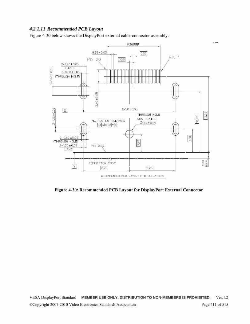
VESA DisplayPort Standard MEMBER USE ONLY. DISTRIBUTION TO NON-MEMBERS IS PROHIBITED. Ver.1.2
©Copyright 2007-2010 Video Electronics Standards Association Page 411 of 515
4.2.1.11 Recommended PCB Layout Figure 4-30 below shows the DisplayPort external cable-connector assembly.
Figure 4-30: Recommended PCB Layout for DisplayPort External Connector
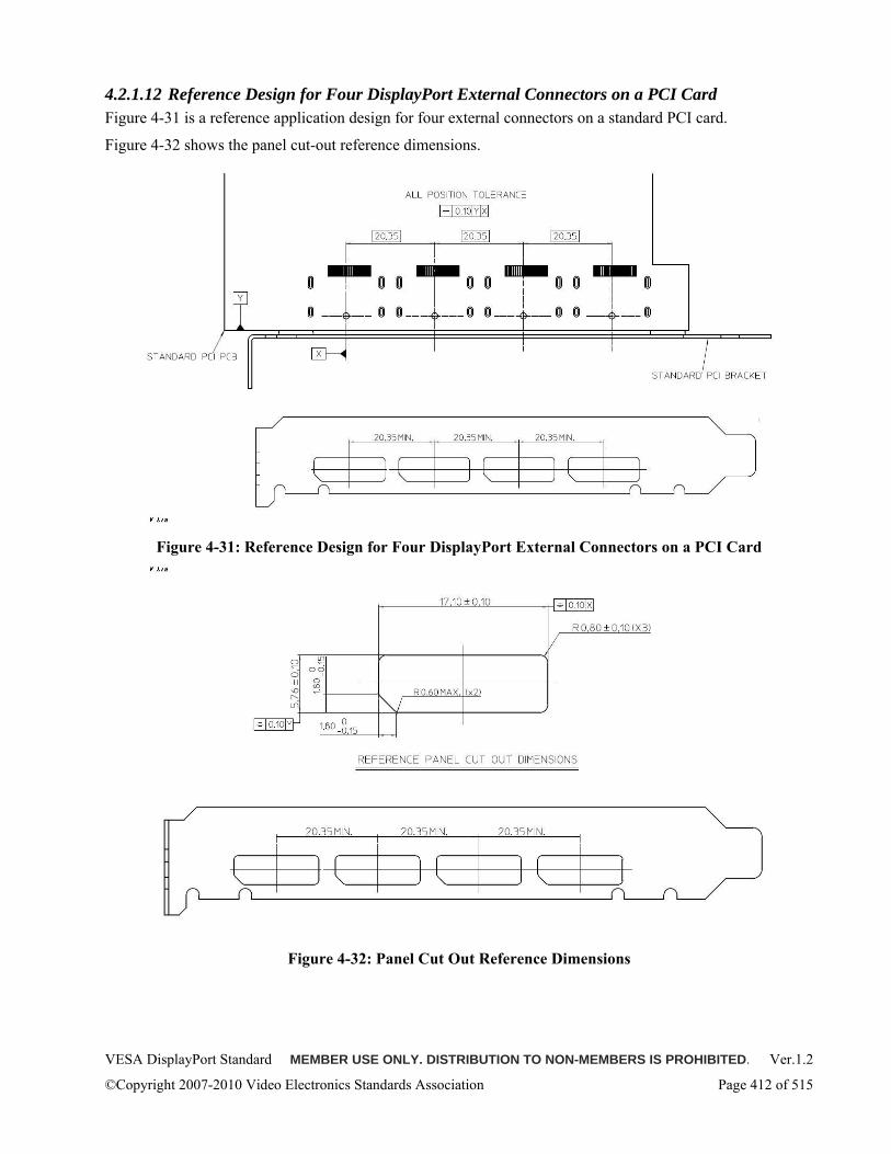
VESA DisplayPort Standard MEMBER USE ONLY. DISTRIBUTION TO NON-MEMBERS IS PROHIBITED. Ver.1.2
©Copyright 2007-2010 Video Electronics Standards Association Page 412 of 515
4.2.1.12 Reference Design for Four DisplayPort External Connectors on a PCI Card Figure 4-31 is a reference application design for four external connectors on a standard PCI card.
Figure 4-32 shows the panel cut-out reference dimensions.
Figure 4-31: Reference Design for Four DisplayPort External Connectors on a PCI Card
Figure 4-32: Panel Cut Out Reference Dimensions
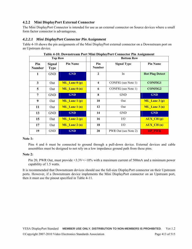
VESA DisplayPort Standard MEMBER USE ONLY. DISTRIBUTION TO NON-MEMBERS IS PROHIBITED. Ver.1.2
©Copyright 2007-2010 Video Electronics Standards Association Page 413 of 515
4.2.2 Mini DisplayPort External Connector The Mini DisplayPort Connector is intended for use as an external connector on Source devices where a small form factor connector is advantageous.
4.2.2.1 Mini DisplayPort Connector Pin Assignment Table 4-10 shows the pin assignments of the Mini DisplayPort external connector on a Downstream port on an Upstream device.
Table 4-10: Downstream Port Mini DisplayPort Connector Pin Assignment Top Row Bottom Row
Pin Number
Signal Type
Pin Name Pin Number
Signal Type Pin Name
1 GND GND 2 In Hot Plug Detect
3 Out ML_Lane 0 (p) 4 CONFIG (see Note 1) CONFIG1
5 Out ML_Lane 0 (n) 6 CONFIG (see Note 1) CONFIG2
7 GND GND 8 GND GND
9 Out ML_Lane 1 (p) 10 Out ML_Lane 3 (p)
11 Out ML_Lane 1 (n) 12 Out ML_Lane 3 (n)
13 GND GND 14 GND GND
15 Out ML_Lane 2 (p) 16 I/O AUX_CH (p)
17 Out ML_Lane 2 (n) 18 I/O AUX_CH (n)
19 GND GND 20 PWR Out (see Note 2) DP_PWR
Note 1:
Pins 4 and 6 must be connected to ground through a pull-down device. External devices and cable assemblies must be designed to not rely on a low impedance ground path from these pins.
Note 2:
Pin 20, PWR Out, must provide +3.3V+/-10% with a maximum current of 500mA and a minimum power capability of 1.5 watts.
It is recommended that Downstream devices should use the full-size DisplayPort connector on their Upstream ports. However, if a Downstream device implements the Mini DisplayPort connector on an Upstream port, then it must use the pinout specified in Table 4-11.
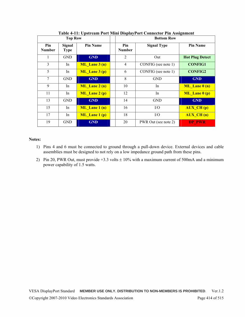
VESA DisplayPort Standard MEMBER USE ONLY. DISTRIBUTION TO NON-MEMBERS IS PROHIBITED. Ver.1.2
©Copyright 2007-2010 Video Electronics Standards Association Page 414 of 515
Table 4-11: Upstream Port Mini DisplayPort Connector Pin Assignment Top Row Bottom Row
Pin Number
Signal Type
Pin Name Pin Number
Signal Type Pin Name
1 GND GND 2 Out Hot Plug Detect
3 In ML_Lane 3 (n) 4 CONFIG (see note 1) CONFIG1
5 In ML_Lane 3 (p) 6 CONFIG (see note 1) CONFIG2
7 GND GND 8 GND GND
9 In ML_Lane 2 (n) 10 In ML_Lane 0 (n)
11 In ML_Lane 2 (p) 12 In ML_Lane 0 (p)
13 GND GND 14 GND GND
15 In ML_Lane 1 (n) 16 I/O AUX_CH (p)
17 In ML_Lane 1 (p) 18 I/O AUX_CH (n)
19 GND GND 20 PWR Out (see note 2) DP_PWR
Notes:
1) Pins 4 and 6 must be connected to ground through a pull-down device. External devices and cable assemblies must be designed to not rely on a low impedance ground path from these pins.
2) Pin 20, PWR Out, must provide +3.3 volts ± 10% with a maximum current of 500mA and a minimum power capability of 1.5 watts.
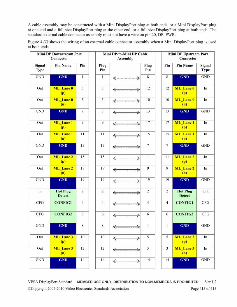
VESA DisplayPort Standard MEMBER USE ONLY. DISTRIBUTION TO NON-MEMBERS IS PROHIBITED. Ver.1.2
©Copyright 2007-2010 Video Electronics Standards Association Page 415 of 515
A cable assembly may be constructed with a Mini DisplayPort plug at both ends, or a Mini DisplayPort plug at one end and a full-size DisplayPort plug at the other end, or a full-size DisplayPort plug at both ends. The standard external cable connector assembly must not have a wire on pin 20, DP_PWR.
Figure 4-33 shows the wiring of an external cable connector assembly when a Mini DisplayPort plug is used at both ends.
Mini DP Downstream Port Connector
Mini DP-to-Mini DP Cable Assembly
Mini DP Upstream Port Connector
Signal Type
Pin Name Pin Plug Pin
Plug Pin
Pin Pin Name Signal Type
GND GND 1 1
8 8 GND GND
Out ML_Lane 0 (p)
3 3
12 12 ML_Lane 0 (p)
In
Out ML_Lane 0 (n)
5 5
10 10 ML_Lane 0 (n)
In
GND GND 7 7
13 13 GND GND
Out ML_Lane 1 (p)
9 9
17 17 ML_Lane 1 (p)
In
Out ML_Lane 1 (n)
11 11
15 15 ML_Lane 1 (n)
In
GND GND 13 13
7 7 GND GND
Out ML_Lane 2 (p)
15 15
11 11 ML_Lane 2 (p)
In
Out ML_Lane 2 (n)
17 17
9 9 ML_Lane 2 (n)
In
GND GND 19 19
19 19 GND GND
In Hot Plug Detect
2 2
2 2 Hot Plug Detect
Out
CFG CONFIG1 4 4
4 4 CONFIG1 CFG
CFG CONFIG2 6 6
6 6 CONFIG2 CFG
GND GND 8 8
1 1 GND GND
Out ML_Lane 3 (p)
10 10
5 5 ML_Lane 3 (p)
In
Out ML_Lane 3 (n)
12 12
3 3 ML_Lane 3 (n)
In
GND GND 14 14
14 14 GND GND
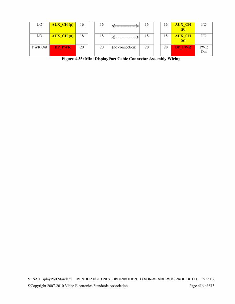
VESA DisplayPort Standard MEMBER USE ONLY. DISTRIBUTION TO NON-MEMBERS IS PROHIBITED. Ver.1.2
©Copyright 2007-2010 Video Electronics Standards Association Page 416 of 515
I/O AUX_CH (p) 16 16
16 16 AUX_CH (p)
I/O
I/O AUX_CH (n) 18 18
18 18 AUX_CH (n)
I/O
PWR Out DP_PWR 20 20 (no connection) 20 20 DP_PWR PWR Out
Figure 4-33: Mini DisplayPort Cable Connector Assembly Wiring
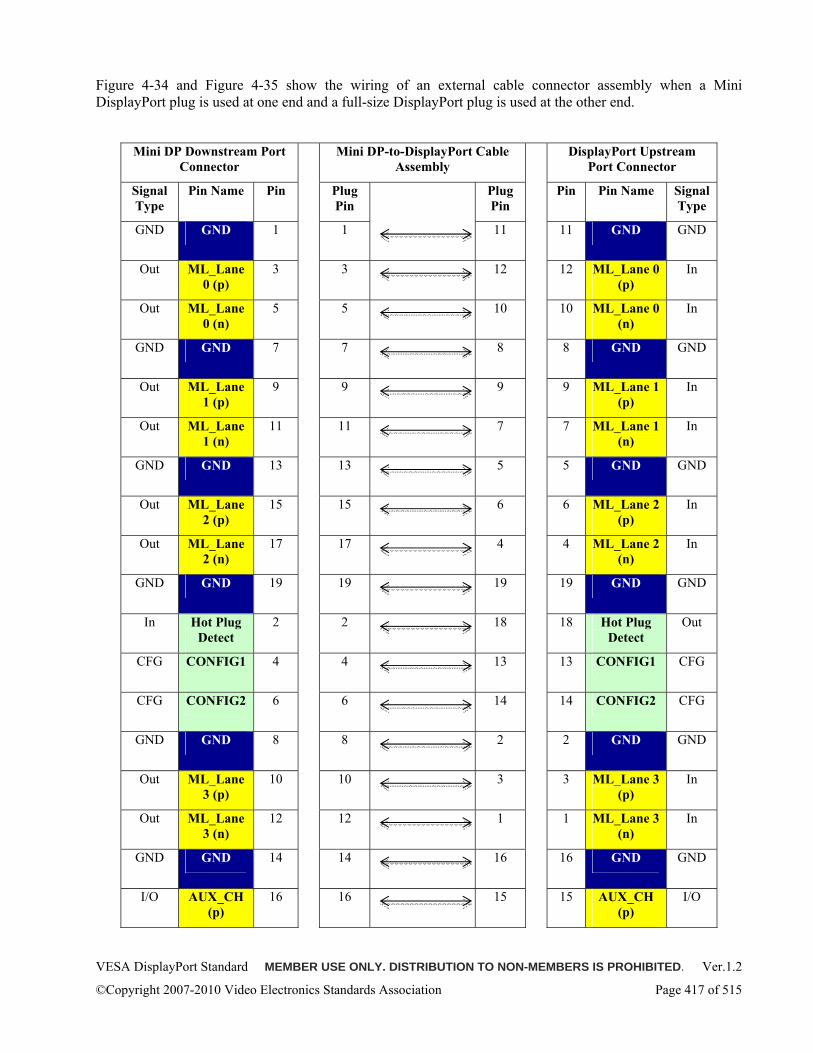
VESA DisplayPort Standard MEMBER USE ONLY. DISTRIBUTION TO NON-MEMBERS IS PROHIBITED. Ver.1.2
©Copyright 2007-2010 Video Electronics Standards Association Page 417 of 515
Figure 4-34 and Figure 4-35 show the wiring of an external cable connector assembly when a Mini DisplayPort plug is used at one end and a full-size DisplayPort plug is used at the other end.
Mini DP Downstream Port Connector
Mini DP-to-DisplayPort Cable Assembly
DisplayPort Upstream Port Connector
Signal Type
Pin Name Pin Plug Pin
Plug Pin
Pin Pin Name Signal Type
GND GND 1 1
11 11 GND GND
Out ML_Lane 0 (p)
3 3
12 12 ML_Lane 0 (p)
In
Out ML_Lane 0 (n)
5 5
10 10 ML_Lane 0 (n)
In
GND GND 7 7
8 8 GND GND
Out ML_Lane 1 (p)
9 9
9 9 ML_Lane 1 (p)
In
Out ML_Lane 1 (n)
11 11
7 7 ML_Lane 1 (n)
In
GND GND 13 13
5 5 GND GND
Out ML_Lane 2 (p)
15 15
6 6 ML_Lane 2 (p)
In
Out ML_Lane 2 (n)
17 17
4 4 ML_Lane 2 (n)
In
GND GND 19 19
19 19 GND GND
In Hot Plug Detect
2 2
18 18 Hot Plug Detect
Out
CFG CONFIG1 4 4
13 13 CONFIG1 CFG
CFG CONFIG2 6 6
14 14 CONFIG2 CFG
GND GND 8 8
2 2 GND GND
Out ML_Lane 3 (p)
10 10
3 3 ML_Lane 3 (p)
In
Out ML_Lane 3 (n)
12 12
1 1 ML_Lane 3 (n)
In
GND GND 14 14
16 16 GND GND
I/O AUX_CH (p)
16 16
15 15 AUX_CH (p)
I/O
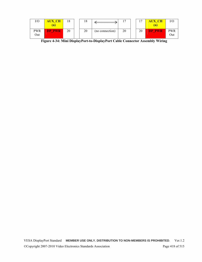
VESA DisplayPort Standard MEMBER USE ONLY. DISTRIBUTION TO NON-MEMBERS IS PROHIBITED. Ver.1.2
©Copyright 2007-2010 Video Electronics Standards Association Page 418 of 515
I/O AUX_CH (n)
18 18
17 17 AUX_CH (n)
I/O
PWR Out
DP_PWR 20 20 (no connection) 20 20 DP_PWR PWR Out
Figure 4-34: Mini DisplayPort-to-DisplayPort Cable Connector Assembly Wiring
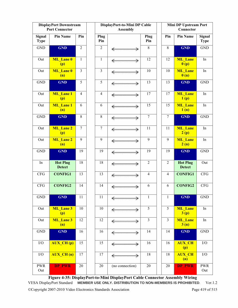
VESA DisplayPort Standard MEMBER USE ONLY. DISTRIBUTION TO NON-MEMBERS IS PROHIBITED. Ver.1.2
©Copyright 2007-2010 Video Electronics Standards Association Page 419 of 515
DisplayPort Downstream Port Connector
DisplayPort-to-Mini DP Cable Assembly
Mini DP Upstream Port Connector
Signal Type
Pin Name Pin Plug Pin
Plug Pin
Pin Pin Name Signal Type
GND GND 2 2
8 8 GND GND
Out ML_Lane 0 (p)
1 1
12 12 ML_Lane 0 (p)
In
Out ML_Lane 0 (n)
3 3
10 10 ML_Lane 0 (n)
In
GND GND 5 5
13 13 GND GND
Out ML_Lane 1 (p)
4 4
17 17 ML_Lane 1 (p)
In
Out ML_Lane 1 (n)
6 6
15 15 ML_Lane 1 (n)
In
GND GND 8 8
7 7 GND GND
Out ML_Lane 2 (p)
7 7
11 11 ML_Lane 2 (p)
In
Out ML_Lane 2 (n)
9 9
9 9 ML_Lane 2 (n)
In
GND GND 19 19
19 19 GND GND
In Hot Plug Detect
18 18
2 2 Hot Plug Detect
Out
CFG CONFIG1 13 13
4 4 CONFIG1 CFG
CFG CONFIG2 14 14
6 6 CONFIG2 CFG
GND GND 11 11
1 1 GND GND
Out ML_Lane 3 (p)
10 10
5 5 ML_Lane 3 (p)
In
Out ML_Lane 3 (n)
12 12
3 3 ML_Lane 3 (n)
In
GND GND 16 16
14 14 GND GND
I/O AUX_CH (p) 15 15
16 16 AUX_CH (p)
I/O
I/O AUX_CH (n) 17 17
18 18 AUX_CH (n)
I/O
PWR Out
DP_PWR 20 20 (no connection) 20 20 DP_PWR PWR Out
Figure 4-35: DisplayPort-to-Mini DisplayPort Cable Connector Assembly Wiring
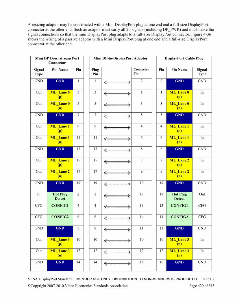
VESA DisplayPort Standard MEMBER USE ONLY. DISTRIBUTION TO NON-MEMBERS IS PROHIBITED. Ver.1.2
©Copyright 2007-2010 Video Electronics Standards Association Page 420 of 515
A resizing adaptor may be constructed with a Mini DisplayPort plug at one end and a full-size DisplayPort connector at the other end. Such an adaptor must carry all 20 signals (including DP_PWR) and must make the signal connections so that the mini DisplayPort plug adapts to a full-size DisplayPort connector. Figure 4-36 shows the wiring of a passive adaptor with a Mini DisplayPort plug at one end and a full-size DisplayPort connector at the other end.
Mini DP Downstream Port Connector
Mini DP-to-DisplayPort Adaptor DisplayPort Cable Plug
Signal Type
Pin Name Pin Plug Pin
Connector Pin
Pin Pin Name Signal Type
GND GND 1 1
2 2 GND GND
Out ML_Lane 0 (p)
3 3
1 1 ML_Lane 0 (p)
In
Out ML_Lane 0 (n)
5 5
3 3 ML_Lane 0 (n)
In
GND GND 7 7
5 5 GND GND
Out ML_Lane 1 (p)
9 9
4 4 ML_Lane 1 (p)
In
Out ML_Lane 1 (n)
11 11
6 6 ML_Lane 1 (n)
In
GND GND 13 13
8 8 GND GND
Out ML_Lane 2 (p)
15 15
7 7 ML_Lane 2 (p)
In
Out ML_Lane 2 (n)
17 17
9 9 ML_Lane 2 (n)
In
GND GND 19 19
19 19 GND GND
In Hot Plug Detect
2 2
18 18 Hot Plug Detect
Out
CFG CONFIG1 4 4
13 13 CONFIG1 CFG
CFG CONFIG2 6 6
14 14 CONFIG2 CFG
GND GND 8 8
11 11 GND GND
Out ML_Lane 3 (p)
10 10
10 10 ML_Lane 3 (p)
In
Out ML_Lane 3 (n)
12 12
12 12 ML_Lane 3 (n)
In
GND GND 14 14
16 16 GND GND
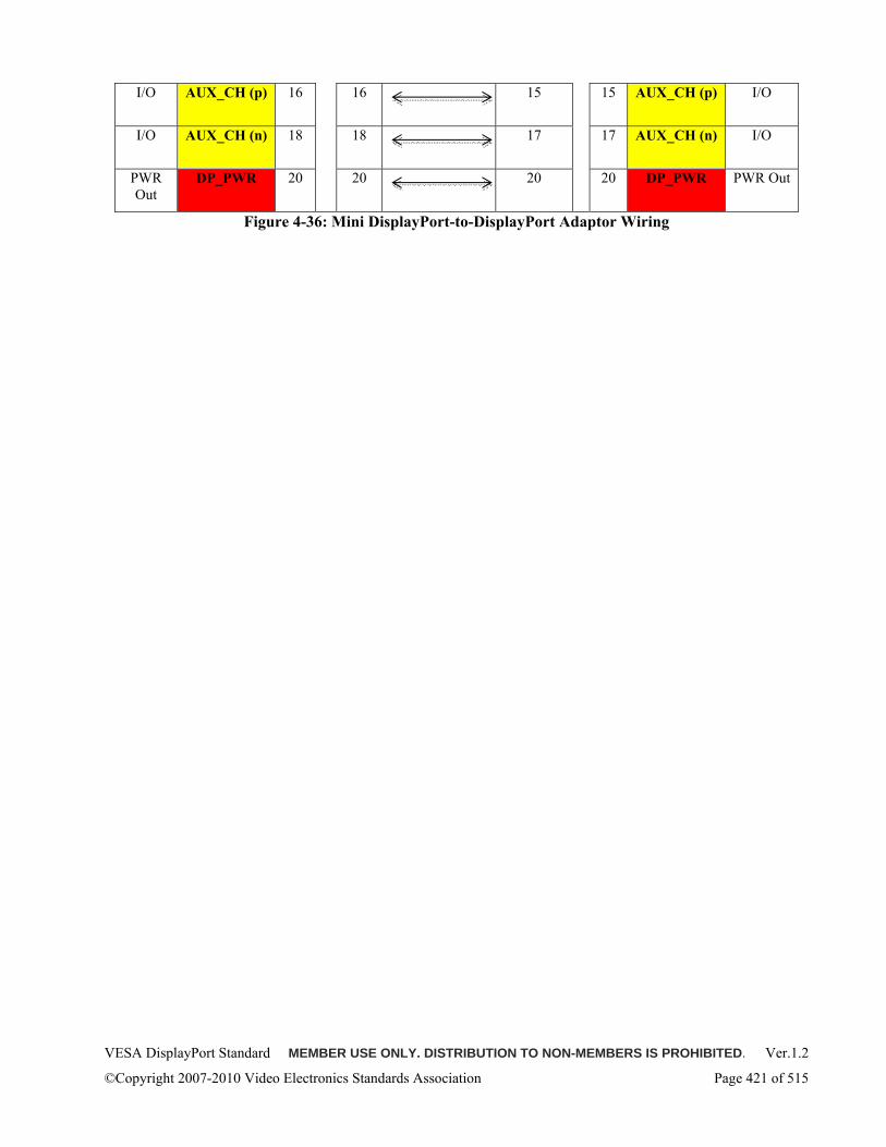
VESA DisplayPort Standard MEMBER USE ONLY. DISTRIBUTION TO NON-MEMBERS IS PROHIBITED. Ver.1.2
©Copyright 2007-2010 Video Electronics Standards Association Page 421 of 515
I/O AUX_CH (p) 16 16
15 15 AUX_CH (p) I/O
I/O AUX_CH (n) 18 18
17 17 AUX_CH (n) I/O
PWR Out
DP_PWR 20 20
20 20 DP_PWR PWR Out
Figure 4-36: Mini DisplayPort-to-DisplayPort Adaptor Wiring
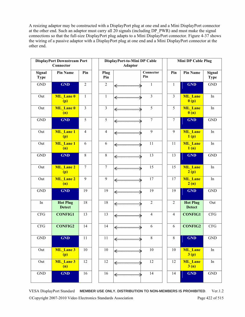
VESA DisplayPort Standard MEMBER USE ONLY. DISTRIBUTION TO NON-MEMBERS IS PROHIBITED. Ver.1.2
©Copyright 2007-2010 Video Electronics Standards Association Page 422 of 515
A resizing adaptor may be constructed with a DisplayPort plug at one end and a Mini DisplayPort connector at the other end. Such an adaptor must carry all 20 signals (including DP_PWR) and must make the signal connections so that the full-size DisplayPort plug adapts to a Mini DisplayPort connector. Figure 4-37 shows the wiring of a passive adaptor with a DisplayPort plug at one end and a Mini DisplayPort connector at the other end.
DisplayPort Downstream Port Connector
DisplayPort-to-Mini DP Cable Adaptor
Mini DP Cable Plug
Signal Type
Pin Name Pin Plug Pin
Connector Pin
Pin Pin Name Signal Type
GND GND 2 2
1 1 GND GND
Out ML_Lane 0 (p)
1 1
3 3 ML_Lane 0 (p)
In
Out ML_Lane 0 (n)
3 3
5 5 ML_Lane 0 (n)
In
GND GND 5 5
7 7 GND GND
Out ML_Lane 1 (p)
4 4
9 9 ML_Lane 1 (p)
In
Out ML_Lane 1 (n)
6 6
11 11 ML_Lane 1 (n)
In
GND GND 8 8
13 13 GND GND
Out ML_Lane 2 (p)
7 7
15 15 ML_Lane 2 (p)
In
Out ML_Lane 2 (n)
9 9
17 17 ML_Lane 2 (n)
In
GND GND 19 19
19 19 GND GND
In Hot Plug Detect
18 18
2 2 Hot Plug Detect
Out
CFG CONFIG1 13 13
4 4 CONFIG1 CFG
CFG CONFIG2 14 14
6 6 CONFIG2 CFG
GND GND 11 11
8 8 GND GND
Out ML_Lane 3 (p)
10 10
10 10 ML_Lane 3 (p)
In
Out ML_Lane 3 (n)
12 12
12 12 ML_Lane 3 (n)
In
GND GND 16 16
14 14 GND GND
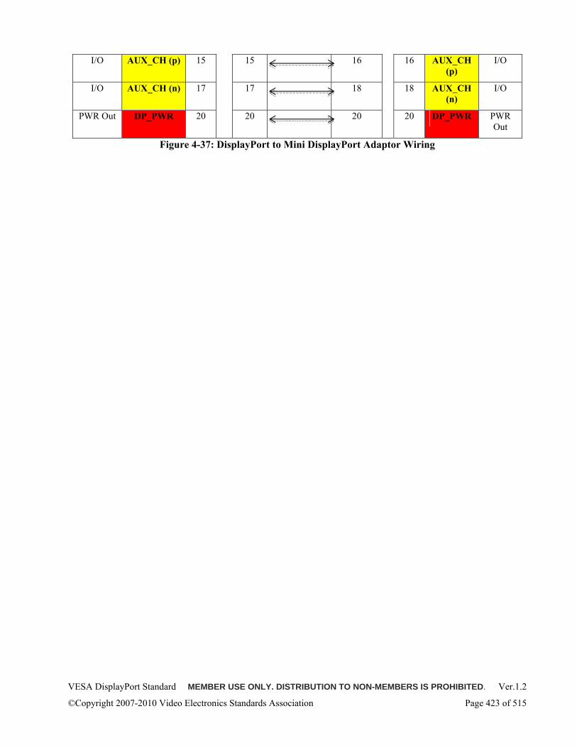
VESA DisplayPort Standard MEMBER USE ONLY. DISTRIBUTION TO NON-MEMBERS IS PROHIBITED. Ver.1.2
©Copyright 2007-2010 Video Electronics Standards Association Page 423 of 515
I/O AUX_CH (p) 15 15
16 16 AUX_CH (p)
I/O
I/O AUX_CH (n) 17 17
18 18 AUX_CH (n)
I/O
PWR Out DP_PWR 20 20
20 20 DP_PWR PWR Out
Figure 4-37: DisplayPort to Mini DisplayPort Adaptor Wiring
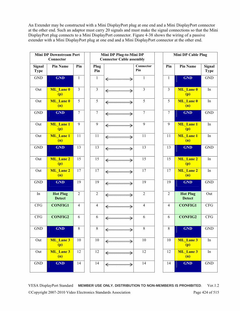
VESA DisplayPort Standard MEMBER USE ONLY. DISTRIBUTION TO NON-MEMBERS IS PROHIBITED. Ver.1.2
©Copyright 2007-2010 Video Electronics Standards Association Page 424 of 515
An Extender may be constructed with a Mini DisplayPort plug at one end and a Mini DisplayPort connector at the other end. Such an adaptor must carry 20 signals and must make the signal connections so that the Mini DisplayPort plug connects to a Mini DisplayPort connector. Figure 4-38 shows the wiring of a passive extender with a Mini DisplayPort plug at one end and a Mini DisplayPort connector at the other end.
Mini DP Downstream Port Connector
Mini DP Plug-to-Mini DP Connector Cable assembly
Mini DP Cable Plug
Signal Type
Pin Name Pin Plug Pin
Connector Pin
Pin Pin Name Signal Type
GND GND 1 1
1 1 GND GND
Out ML_Lane 0 (p)
3 3
3 3 ML_Lane 0 (p)
In
Out ML_Lane 0 (n)
5 5
5 5 ML_Lane 0 (n)
In
GND GND 7 7
7 7 GND GND
Out ML_Lane 1 (p)
9 9
9 9 ML_Lane 1 (p)
In
Out ML_Lane 1 (n)
11 11
11 11 ML_Lane 1 (n)
In
GND GND 13 13
13 13 GND GND
Out ML_Lane 2 (p)
15 15
15 15 ML_Lane 2 (p)
In
Out ML_Lane 2 (n)
17 17
17 17 ML_Lane 2 (n)
In
GND GND 19 19
19 19 GND GND
In Hot Plug Detect
2 2
2 2 Hot Plug Detect
Out
CFG CONFIG1 4 4
4 4 CONFIG1 CFG
CFG CONFIG2 6 6
6 6 CONFIG2 CFG
GND GND 8 8
8 8 GND GND
Out ML_Lane 3 (p)
10 10
10 10 ML_Lane 3 (p)
In
Out ML_Lane 3 (n)
12 12
12 12 ML_Lane 3 (n)
In
GND GND 14 14
14 14 GND GND
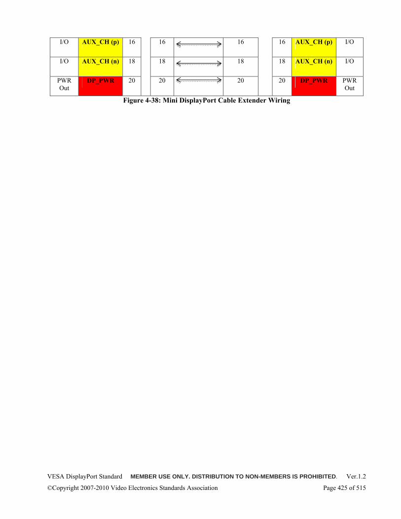
VESA DisplayPort Standard MEMBER USE ONLY. DISTRIBUTION TO NON-MEMBERS IS PROHIBITED. Ver.1.2
©Copyright 2007-2010 Video Electronics Standards Association Page 425 of 515
I/O AUX_CH (p) 16 16
16 16 AUX_CH (p) I/O
I/O AUX_CH (n) 18 18
18 18 AUX_CH (n) I/O
PWR Out
DP_PWR 20 20
20 20 DP_PWR PWR Out
Figure 4-38: Mini DisplayPort Cable Extender Wiring
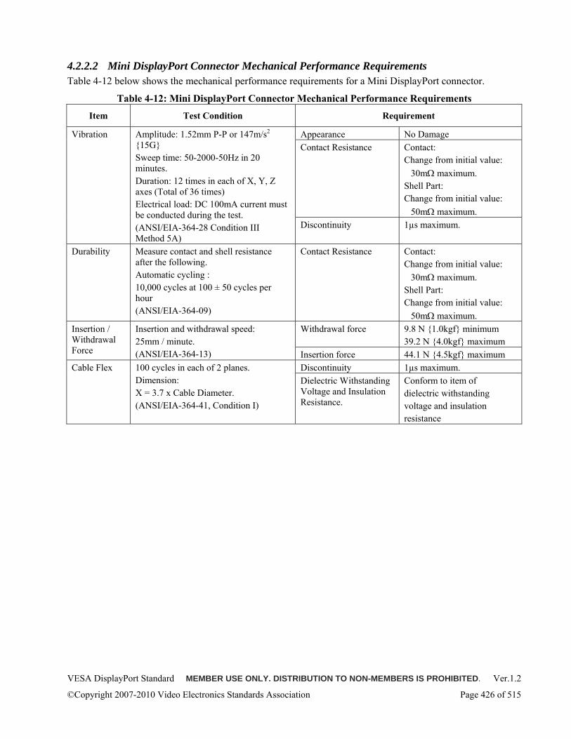
VESA DisplayPort Standard MEMBER USE ONLY. DISTRIBUTION TO NON-MEMBERS IS PROHIBITED. Ver.1.2
©Copyright 2007-2010 Video Electronics Standards Association Page 426 of 515
4.2.2.2 Mini DisplayPort Connector Mechanical Performance Requirements Table 4-12 below shows the mechanical performance requirements for a Mini DisplayPort connector.
Table 4-12: Mini DisplayPort Connector Mechanical Performance Requirements
Item Test Condition Requirement
Appearance No Damage Contact Resistance Contact:
Change from initial value: 30mΩ maximum.
Shell Part: Change from initial value:
50mΩ maximum.
Vibration Amplitude: 1.52mm P-P or 147m/s2 15G Sweep time: 50-2000-50Hz in 20 minutes. Duration: 12 times in each of X, Y, Z axes (Total of 36 times) Electrical load: DC 100mA current must be conducted during the test. (ANSI/EIA-364-28 Condition III Method 5A)
Discontinuity 1µs maximum.
Durability Measure contact and shell resistance after the following. Automatic cycling : 10,000 cycles at 100 ± 50 cycles per hour (ANSI/EIA-364-09)
Contact Resistance Contact: Change from initial value:
30mΩ maximum. Shell Part: Change from initial value:
50mΩ maximum. Withdrawal force 9.8 N 1.0kgf minimum
39.2 N 4.0kgf maximum Insertion / Withdrawal Force
Insertion and withdrawal speed: 25mm / minute. (ANSI/EIA-364-13) Insertion force 44.1 N 4.5kgf maximum
Discontinuity 1µs maximum. Cable Flex 100 cycles in each of 2 planes. Dimension: X = 3.7 x Cable Diameter. (ANSI/EIA-364-41, Condition I)
Dielectric Withstanding Voltage and Insulation Resistance.
Conform to item of dielectric withstanding voltage and insulation resistance
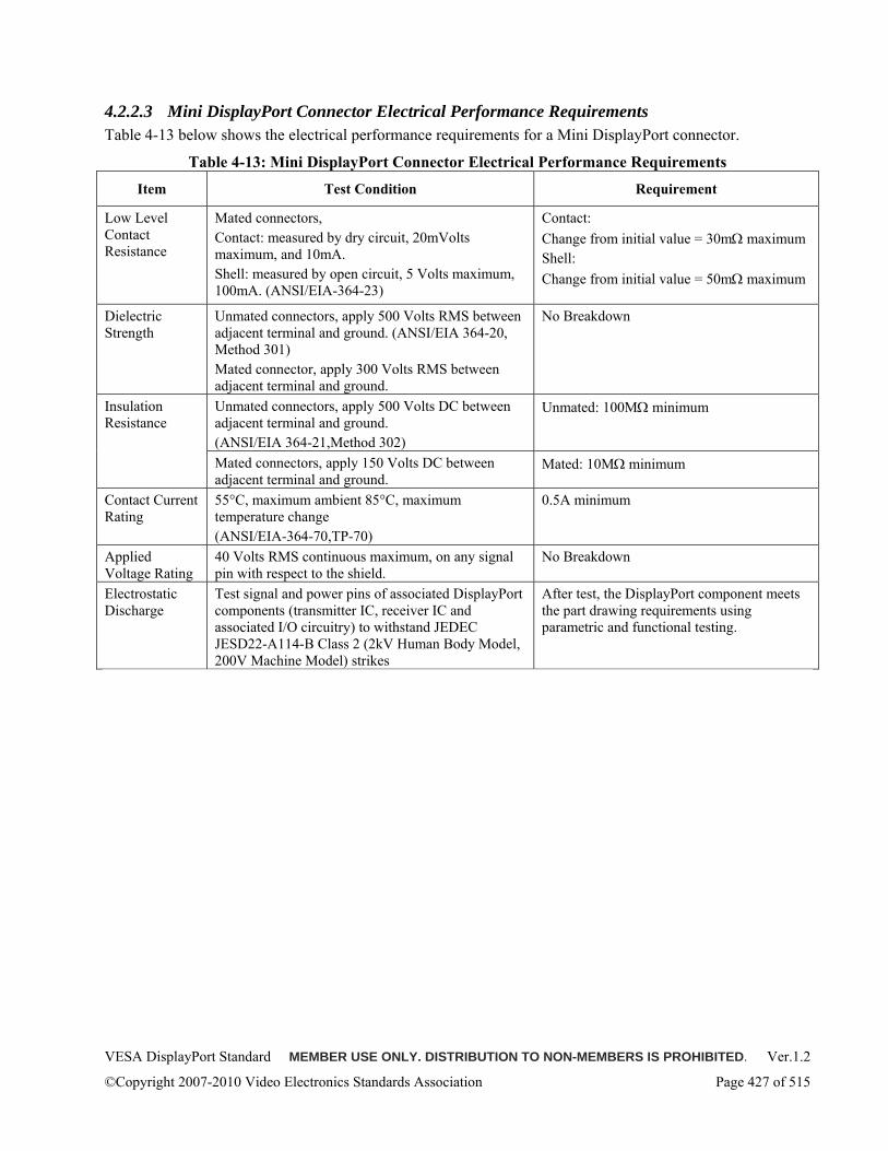
VESA DisplayPort Standard MEMBER USE ONLY. DISTRIBUTION TO NON-MEMBERS IS PROHIBITED. Ver.1.2
©Copyright 2007-2010 Video Electronics Standards Association Page 427 of 515
4.2.2.3 Mini DisplayPort Connector Electrical Performance Requirements Table 4-13 below shows the electrical performance requirements for a Mini DisplayPort connector.
Table 4-13: Mini DisplayPort Connector Electrical Performance Requirements
Item Test Condition Requirement
Low Level Contact Resistance
Mated connectors, Contact: measured by dry circuit, 20mVolts maximum, and 10mA. Shell: measured by open circuit, 5 Volts maximum, 100mA. (ANSI/EIA-364-23)
Contact: Change from initial value = 30mΩ maximum Shell: Change from initial value = 50mΩ maximum
Dielectric Strength
Unmated connectors, apply 500 Volts RMS between adjacent terminal and ground. (ANSI/EIA 364-20, Method 301) Mated connector, apply 300 Volts RMS between adjacent terminal and ground.
No Breakdown
Unmated connectors, apply 500 Volts DC between adjacent terminal and ground. (ANSI/EIA 364-21,Method 302)
Unmated: 100MΩ minimum Insulation Resistance
Mated connectors, apply 150 Volts DC between adjacent terminal and ground.
Mated: 10MΩ minimum
Contact Current Rating
55°C, maximum ambient 85°C, maximum temperature change (ANSI/EIA-364-70,TP-70)
0.5A minimum
Applied Voltage Rating
40 Volts RMS continuous maximum, on any signal pin with respect to the shield.
No Breakdown
Electrostatic Discharge
Test signal and power pins of associated DisplayPort components (transmitter IC, receiver IC and associated I/O circuitry) to withstand JEDEC JESD22-A114-B Class 2 (2kV Human Body Model, 200V Machine Model) strikes
After test, the DisplayPort component meets the part drawing requirements using parametric and functional testing.
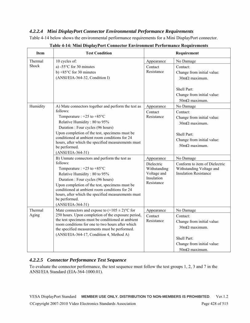
VESA DisplayPort Standard MEMBER USE ONLY. DISTRIBUTION TO NON-MEMBERS IS PROHIBITED. Ver.1.2
©Copyright 2007-2010 Video Electronics Standards Association Page 428 of 515
4.2.2.4 Mini DisplayPort Connector Environmental Performance Requirements Table 4-14 below shows the environmental performance requirements for a Mini DisplayPort connector.
Table 4-14: Mini DisplayPort Connector Environment Performance Requirements
Item Test Condition Requirement
Appearance No Damage Thermal Shock
10 cycles of: a) -55°C for 30 minutes b) +85°C for 30 minutes (ANSI/EIA-364-32, Condition I)
Contact Resistance
Contact: Change from initial value:
30mΩ maximum. Shell Part: Change from initial value:
50mΩ maximum. Appearance No Damage A) Mate connectors together and perform the test as
follows: Temperature : +25 to +85°C Relative Humidity : 80 to 95% Duration : Four cycles (96 hours)
Upon completion of the test, specimens must be conditioned at ambient room conditions for 24 hours, after which the specified measurements must be performed. (ANSI/EIA-364-31)
Contact Resistance
Contact: Change from initial value:
30mΩ maximum. Shell Part: Change from initial value:
50mΩ maximum.
Appearance No Damage
Humidity
B) Unmate connectors and perform the test as follows:
Temperature : +25 to +85°C Relative Humidity : 80 to 95% Duration : Four cycles (96 hours)
Upon completion of the test, specimens must be conditioned at ambient room conditions for 24 hours, after which the specified measurements must be performed. (ANSI/EIA-364-31)
Dielectric Withstanding Voltage and Insulation Resistance
Conform to item of Dielectric Withstanding Voltage and Insulation Resistance
Appearance No Damage Thermal Aging
Mate connectors and expose to (+105 ± 2)°C for 250 hours. Upon completion of the exposure period, the test specimens must be conditioned at ambient room conditions for one to two hours after which the specified measurements must be performed. (ANSI/EIA-364-17, Condition 4, Method A)
Contact Resistance
Contact: Change from initial value:
30mΩ maximum. Shell Part: Change from initial value:
50mΩ maximum.
4.2.2.5 Connector Performance Test Sequence To evaluate the connector performance, the test sequence must follow the test groups 1, 2, 3 and 7 in the ANSI/EIA Standard (EIA-364-1000.01).
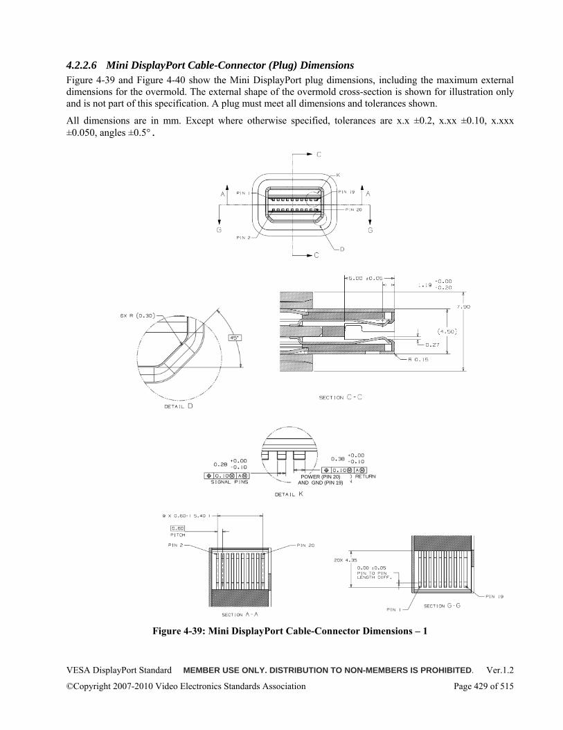
VESA DisplayPort Standard MEMBER USE ONLY. DISTRIBUTION TO NON-MEMBERS IS PROHIBITED. Ver.1.2
©Copyright 2007-2010 Video Electronics Standards Association Page 429 of 515
4.2.2.6 Mini DisplayPort Cable-Connector (Plug) Dimensions Figure 4-39 and Figure 4-40 show the Mini DisplayPort plug dimensions, including the maximum external dimensions for the overmold. The external shape of the overmold cross-section is shown for illustration only and is not part of this specification. A plug must meet all dimensions and tolerances shown.
All dimensions are in mm. Except where otherwise specified, tolerances are x.x ±0.2, x.xx ±0.10, x.xxx ±0.050, angles ±0.5°.
Figure 4-39: Mini DisplayPort Cable-Connector Dimensions – 1
POWER (PIN 20) AND GND (PIN 19)
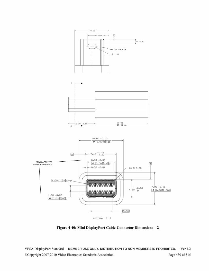
VESA DisplayPort Standard MEMBER USE ONLY. DISTRIBUTION TO NON-MEMBERS IS PROHIBITED. Ver.1.2
©Copyright 2007-2010 Video Electronics Standards Association Page 430 of 515
Figure 4-40: Mini DisplayPort Cable-Connector Dimensions – 2
B
(DIMS APPLY TO TONGUE OPENING)
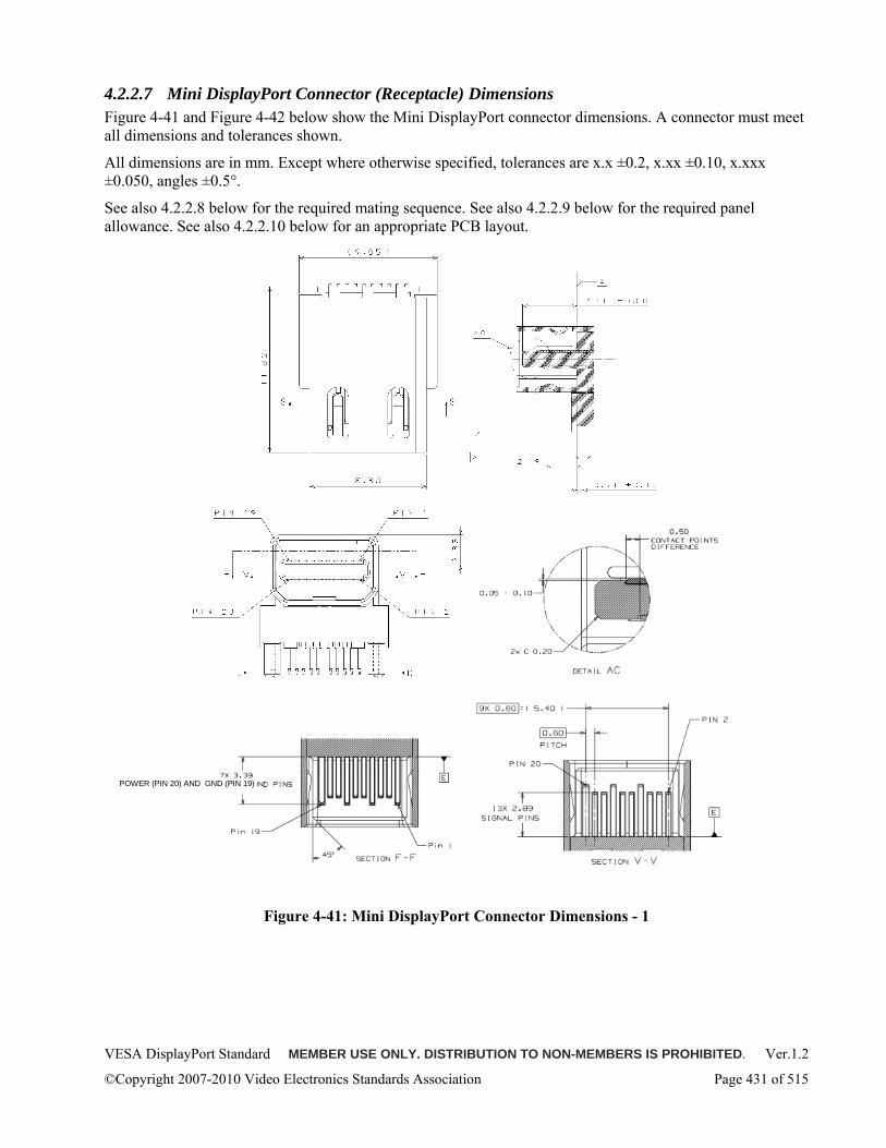
VESA DisplayPort Standard MEMBER USE ONLY. DISTRIBUTION TO NON-MEMBERS IS PROHIBITED. Ver.1.2
©Copyright 2007-2010 Video Electronics Standards Association Page 431 of 515
4.2.2.7 Mini DisplayPort Connector (Receptacle) Dimensions Figure 4-41 and Figure 4-42 below show the Mini DisplayPort connector dimensions. A connector must meet all dimensions and tolerances shown.
All dimensions are in mm. Except where otherwise specified, tolerances are x.x ±0.2, x.xx ±0.10, x.xxx ±0.050, angles ±0.5°.
See also 4.2.2.8 below for the required mating sequence. See also 4.2.2.9 below for the required panel allowance. See also 4.2.2.10 below for an appropriate PCB layout.
Figure 4-41: Mini DisplayPort Connector Dimensions - 1
POWER (PIN 20) AND GND (PIN 19)
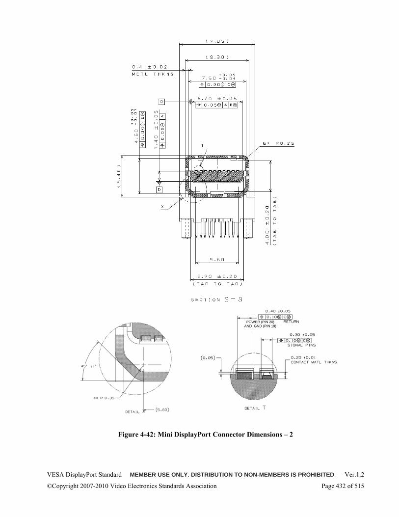
VESA DisplayPort Standard MEMBER USE ONLY. DISTRIBUTION TO NON-MEMBERS IS PROHIBITED. Ver.1.2
©Copyright 2007-2010 Video Electronics Standards Association Page 432 of 515
Figure 4-42: Mini DisplayPort Connector Dimensions – 2
POWER (PIN 20) AND GND (PIN 19)
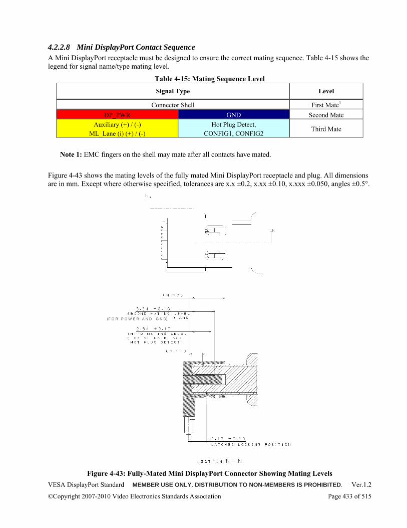
VESA DisplayPort Standard MEMBER USE ONLY. DISTRIBUTION TO NON-MEMBERS IS PROHIBITED. Ver.1.2
©Copyright 2007-2010 Video Electronics Standards Association Page 433 of 515
4.2.2.8 Mini DisplayPort Contact Sequence A Mini DisplayPort receptacle must be designed to ensure the correct mating sequence. Table 4-15 shows the legend for signal name/type mating level.
Table 4-15: Mating Sequence Level
Signal Type Level
Connector Shell First Mate1 DP_PWR GND Second Mate
Auxiliary (+) / (-) ML_Lane (i) (+) / (-)
Hot Plug Detect, CONFIG1, CONFIG2
Third Mate
Note 1: EMC fingers on the shell may mate after all contacts have mated.
Figure 4-43 shows the mating levels of the fully mated Mini DisplayPort receptacle and plug. All dimensions are in mm. Except where otherwise specified, tolerances are x.x ±0.2, x.xx ±0.10, x.xxx ±0.050, angles ±0.5°.
Figure 4-43: Fully-Mated Mini DisplayPort Connector Showing Mating Levels
(F O R P O W E R A N D G N D)
VESA DisplayPort Standard MEMBER USE ONLY. DISTRIBUTION TO NON-MEMBERS IS PROHIBITED. Ver.1.2
©Copyright 2007-2010 Video Electronics Standards Association Page 434 of 515
4.2.2.9 Mini DisplayPort Panel Allowances The figure in the previous section shows the plug protrusion in the fully-mated condition of the plug and the board receptacles. The system design incorporating a Mini DisplayPort receptacle must be designed so that a Mini DisplayPort plug fully mates with the Mini DisplayPort receptacle with appropriate margin, but with sufficient control to prevent an incorrect contact sequence due to angled insertion. The receptacle design must provide an appropriate allowance for a panel, bezel or similar (when used) so that this requirement is met. To meet these requirements, the distance from datum E in the receptacle to the externally accessible mating interface on the device shall be at least 5.7mm and shall not exceed 8.0mm.
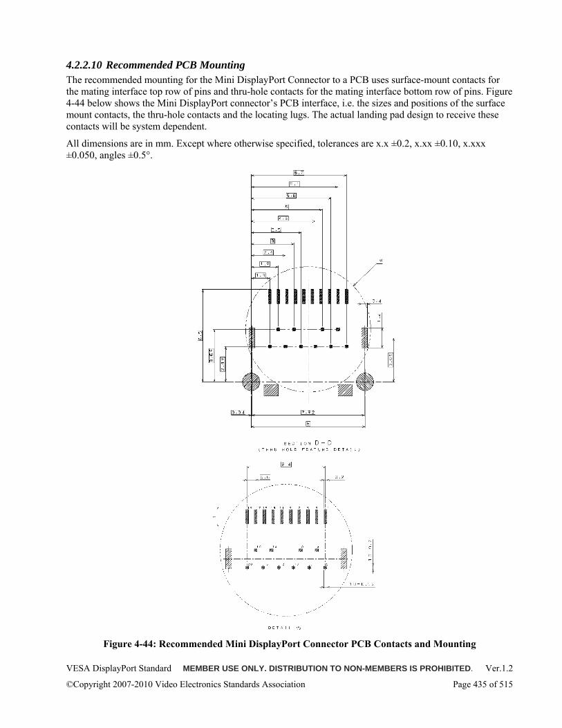
VESA DisplayPort Standard MEMBER USE ONLY. DISTRIBUTION TO NON-MEMBERS IS PROHIBITED. Ver.1.2
©Copyright 2007-2010 Video Electronics Standards Association Page 435 of 515
4.2.2.10 Recommended PCB Mounting The recommended mounting for the Mini DisplayPort Connector to a PCB uses surface-mount contacts for the mating interface top row of pins and thru-hole contacts for the mating interface bottom row of pins. Figure 4-44 below shows the Mini DisplayPort connector’s PCB interface, i.e. the sizes and positions of the surface mount contacts, the thru-hole contacts and the locating lugs. The actual landing pad design to receive these contacts will be system dependent.
All dimensions are in mm. Except where otherwise specified, tolerances are x.x ±0.2, x.xx ±0.10, x.xxx ±0.050, angles ±0.5°.
Figure 4-44: Recommended Mini DisplayPort Connector PCB Contacts and Mounting
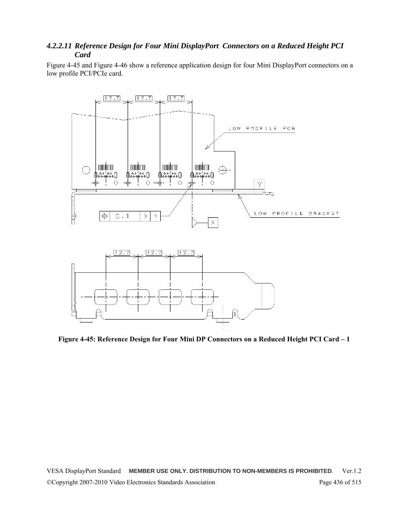
VESA DisplayPort Standard MEMBER USE ONLY. DISTRIBUTION TO NON-MEMBERS IS PROHIBITED. Ver.1.2
©Copyright 2007-2010 Video Electronics Standards Association Page 436 of 515
4.2.2.11 Reference Design for Four Mini DisplayPort Connectors on a Reduced Height PCI Card
Figure 4-45 and Figure 4-46 show a reference application design for four Mini DisplayPort connectors on a low profile PCI/PCIe card.
Figure 4-45: Reference Design for Four Mini DP Connectors on a Reduced Height PCI Card – 1
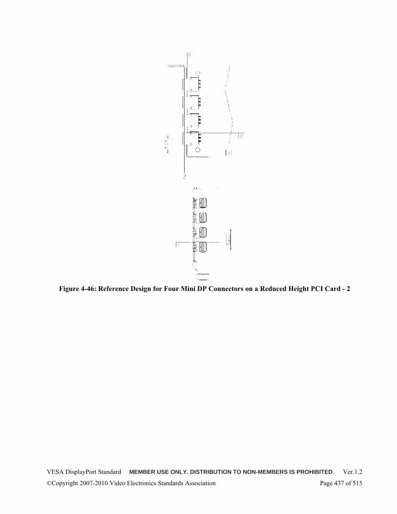
VESA DisplayPort Standard MEMBER USE ONLY. DISTRIBUTION TO NON-MEMBERS IS PROHIBITED. Ver.1.2
©Copyright 2007-2010 Video Electronics Standards Association Page 437 of 515
Figure 4-46: Reference Design for Four Mini DP Connectors on a Reduced Height PCI Card - 2
VESA DisplayPort Standard MEMBER USE ONLY. DISTRIBUTION TO NON-MEMBERS IS PROHIBITED. Ver.1.2
©Copyright 2007-2010 Video Electronics Standards Association Page 438 of 515
4.2.3 Panel-side Internal Connector (Informative) This section covers the specifications for DispayPort panel-side internal connector for reference purposes.
The DisplayPort panel-side internal connector specification is defined in VESA DisplayPort Panel Connector Standard Version 1.
The panel-side internal connector consist of a two-piece, 30-position, low-profile, cable-to-board, co-planar connector. One piece terminates the cable (Plug) and the other is attached to the PCB (Receptacle).
The connector supports up to four Main Link lanes (Lane 0 - Lane 3). In an embedded connection, the cable connector assembly may support one, two, or four lanes depending on the bandwidth requirement of the application.
For one lane and two lane Main Link configurations, the stuffing rule must be:
• When only two lanes are needed, Lane 0 and Lane 1 must be populated while Lane 2 and Lane 3 are unpopulated.
• When only one lane is needed, Lane 0 must be populated while Lane 1 to Lane 3 are unpopulated.
Only the panel TCON (timing controller) side of the connector is defined in this specification. While some cables may have the same connectors on both ends of the cable-connector assembly, others may have more pins for the Source Device side (that is, the side of graphics processor, LCD controller, etc.) for LCD backlight control, for instance.
VESA DisplayPort Standard MEMBER USE ONLY. DISTRIBUTION TO NON-MEMBERS IS PROHIBITED. Ver.1.2
©Copyright 2007-2010 Video Electronics Standards Association Page 439 of 515
4.2.3.1 Panel-side Internal Connector Pin Assignment Table 4-16 below shows the pin assignment of the DisplayPort panel-side internal connector. Pin assignment of those pins other than the DispayPort Main Link and AUX CH in Table 4-16 is for reference purpose only. For pin 1 location, refer to Figure 4-47 below.
Table 4-16: DisplayPort Panel-side Internal Connector Pin Assignment Pin Number Pin Name Pin Definition
Frame Outer shell 1 Reserved2 LCDVCC3 LCDVCC4 LCDVCC5 LCDVCC
Power to LCD panel.
6 GND7 GND8 GND9 GND
Power Return (Ground)
10 Hot Plug Detect Hot Plug Detect Optional 11 Reserved12 Reserved13 H_GND High Speed (Main Link) Ground 14 ML_Lane 3(n) ‘Complement’ Signal-Main Link 15 ML_Lane 3(p) ‘True’ Signal-Main Link 16 H_GND High Speed (Main Link) Ground 17 ML_Lane 2(n) ‘Complement’ Signal-Main Link 18 ML_Lane 2(p) ‘True’ Signal-Main Link 19 H_GND High Speed (Main Link) Ground 20 ML_Lane 1(n) ‘Complement’ Signal-Main Link 21 ML_Lane 1(p) ‘True’ Signal-Main Link 22 H_GND High Speed (Main Link) Ground 23 ML_Lane 0(n) ‘Complement’ Signal-Main Link 24 ML_Lane 0(p) ‘True’ Signal-Main Link 25 H_GND High Speed (Main Link) Ground 26 AUX_CH (p) ‘True’ Signal – Auxiliary channel27 AUX_CH (n) ‘Complement’ Signal – Auxiliary
h l28 H_GND High Speed (Main Link) Ground 29 AUX_PWR +3.3 Trickle PWR 30 Reserved
Frame Outer shell
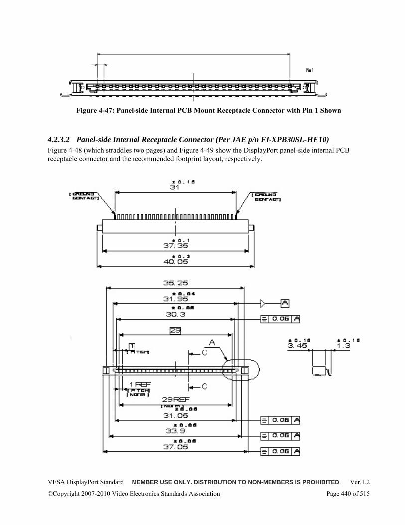
VESA DisplayPort Standard MEMBER USE ONLY. DISTRIBUTION TO NON-MEMBERS IS PROHIBITED. Ver.1.2
©Copyright 2007-2010 Video Electronics Standards Association Page 440 of 515
Figure 4-47: Panel-side Internal PCB Mount Receptacle Connector with Pin 1 Shown
4.2.3.2 Panel-side Internal Receptacle Connector (Per JAE p/n FI-XPB30SL-HF10) Figure 4-48 (which straddles two pages) and Figure 4-49 show the DisplayPort panel-side internal PCB receptacle connector and the recommended footprint layout, respectively.
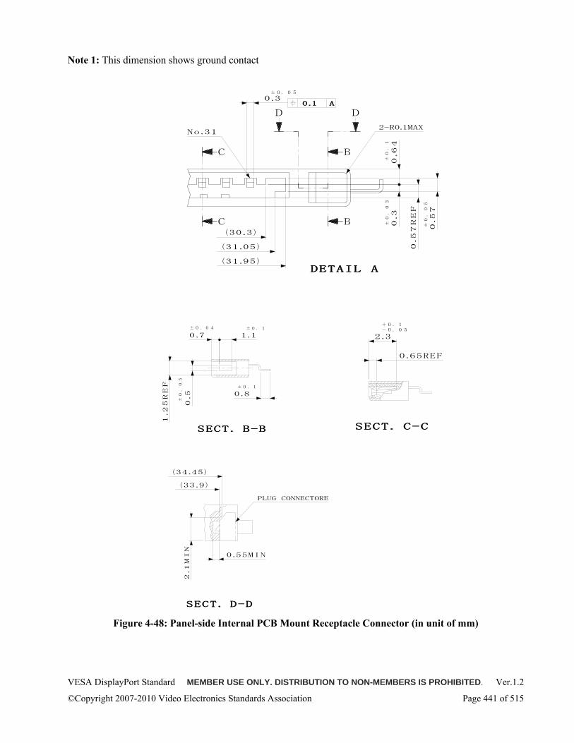
VESA DisplayPort Standard MEMBER USE ONLY. DISTRIBUTION TO NON-MEMBERS IS PROHIBITED. Ver.1.2
©Copyright 2007-2010 Video Electronics Standards Association Page 441 of 515
Note 1: This dimension shows ground contact
Figure 4-48: Panel-side Internal PCB Mount Receptacle Connector (in unit of mm)
SECT. B-B
0.5
0.7 1.1±0.04 ±0.1
±0
.0
5
1.25REF
0.8±0.1
SECT. D-D
0.55MIN
PLUG CONNECTORE
(33.9)
(34.45)
2.1MIN
SECT. C-C
2.3-0.05+0.1
0.65REF
DETAIL A
B
B
C
C
(31.05)
(31.95)
(30.3)
0.3
No.312-R0.1MAX
0.57
±0
.0
3
0.3
0.57REF
±0
.0
5
±0
.1
DD0.1 A
0.64
±0.05
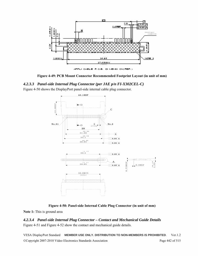
VESA DisplayPort Standard MEMBER USE ONLY. DISTRIBUTION TO NON-MEMBERS IS PROHIBITED. Ver.1.2
©Copyright 2007-2010 Video Electronics Standards Association Page 442 of 515
Figure 4-49: PCB Mount Connector Recommended Footprint Layout (in unit of mm)
4.2.3.3 Panel-side Internal Plug Connector (per JAE p/n FI-X302CEL-C) Figure 4-50 shows the DisplayPort panel-side internal cable plug connector.
1.55
±0
.1
5
0.75REF
0.3REF
(PITCH)
1
29
40.1REF
31.88A
0.05 A
0.05 A34.1
36.85
D
D
±0.03
±0.05
±0.05
No.2No.31
C
12.3REF
30.9MIN(NOTE1)
30.85
30.50.05 A
0.05 A
±0.05
±0.05 A
Figure 4-50: Panel-side Internal Cable Plug Connector (in unit of mm)
Note 1: This is ground area
4.2.3.4 Panel-side Internal Plug Connector – Contact and Mechanical Guide Details Figure 4-51 and Figure 4-52 show the contact and mechanical guide details.
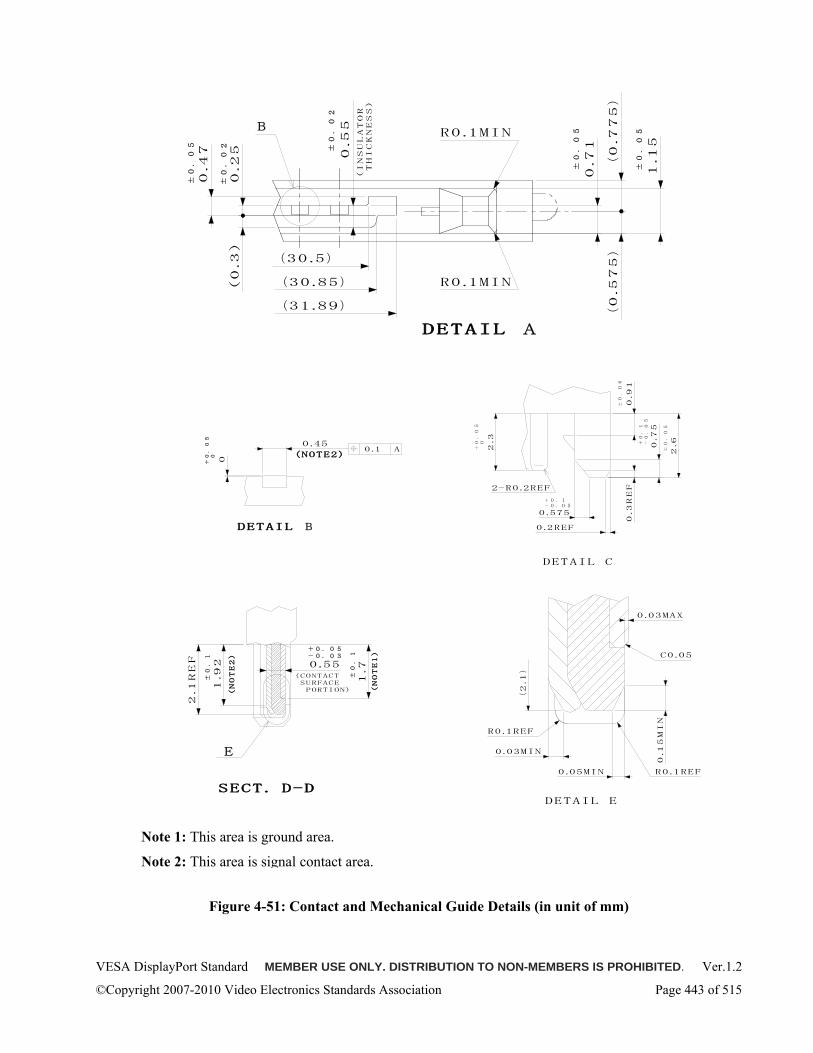
VESA DisplayPort Standard MEMBER USE ONLY. DISTRIBUTION TO NON-MEMBERS IS PROHIBITED. Ver.1.2
©Copyright 2007-2010 Video Electronics Standards Association Page 443 of 515
Figure 4-51: Contact and Mechanical Guide Details (in unit of mm)
DETAIL B
0.450.1 A
0 0
+0
.0
5
(NOTE2)
DETAIL C
2.3
2.6
0.575
0.75
0.91
0.3REF
0.2REF
2-R0.2REF
±0
.0
6
±0
.0
5
-0
.0
5+
0.
1
-0.05+0.1
0
+0
.0
5
SECT. D-D
(CONTACT SURFACE PORTION)
-0.03+0.05
0.55
1.92
(NOTE2)
±0
.1
1.7
(NOTE1)
±0
.1
2.1REF
E
DETAIL E
0.05MIN
0.15MIN
C0.05
0.03MAX
R0.1REF
R0.1REF
0.03MIN
(2.1)
DETAIL A
1.15
±0
.0
5
(31.89)
R0.1MIN
R0.1MIN
0.55
0.71
(0.3)
0.25
0.47
±0
.0
2 ±0
.0
2
±0
.0
5
±0
.0
5
(30.85)
(30.5)
(INSULATOR
THICKNESS)
(0.575)
B
(0.775)
Note 1: This area is ground area.
Note 2: This area is signal contact area.
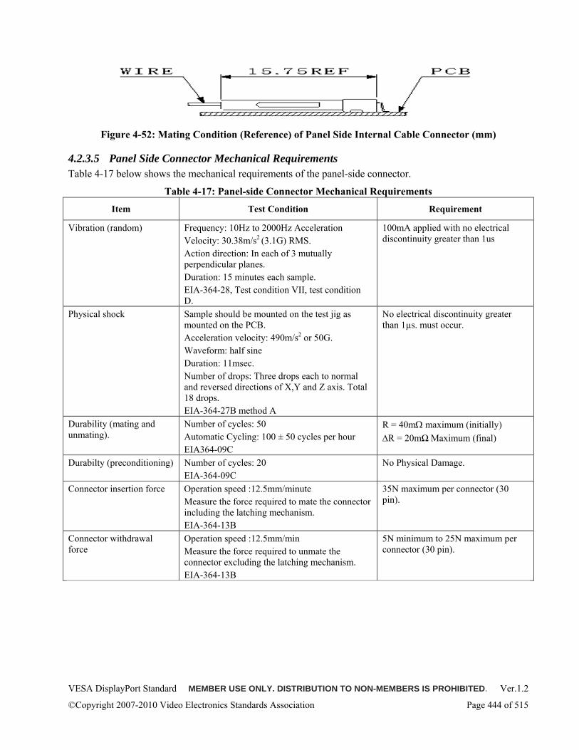
VESA DisplayPort Standard MEMBER USE ONLY. DISTRIBUTION TO NON-MEMBERS IS PROHIBITED. Ver.1.2
©Copyright 2007-2010 Video Electronics Standards Association Page 444 of 515
Figure 4-52: Mating Condition (Reference) of Panel Side Internal Cable Connector (mm)
4.2.3.5 Panel Side Connector Mechanical Requirements Table 4-17 below shows the mechanical requirements of the panel-side connector.
Table 4-17: Panel-side Connector Mechanical Requirements
Item Test Condition Requirement
Vibration (random) Frequency: 10Hz to 2000Hz Acceleration Velocity: 30.38m/s2 (3.1G) RMS. Action direction: In each of 3 mutually perpendicular planes. Duration: 15 minutes each sample. EIA-364-28, Test condition VII, test condition D.
100mA applied with no electrical discontinuity greater than 1us
Physical shock Sample should be mounted on the test jig as mounted on the PCB. Acceleration velocity: 490m/s2 or 50G. Waveform: half sine Duration: 11msec. Number of drops: Three drops each to normal and reversed directions of X,Y and Z axis. Total 18 drops. EIA-364-27B method A
No electrical discontinuity greater than 1µs. must occur.
Durability (mating and unmating).
Number of cycles: 50 Automatic Cycling: 100 ± 50 cycles per hour EIA364-09C
R = 40mΩ maximum (initially) ΔR = 20mΩ Maximum (final)
Durabilty (preconditioning) Number of cycles: 20 EIA-364-09C
No Physical Damage.
Connector insertion force Operation speed :12.5mm/minute Measure the force required to mate the connector including the latching mechanism. EIA-364-13B
35N maximum per connector (30 pin).
Connector withdrawal force
Operation speed :12.5mm/min Measure the force required to unmate the connector excluding the latching mechanism. EIA-364-13B
5N minimum to 25N maximum per connector (30 pin).
VESA DisplayPort Standard MEMBER USE ONLY. DISTRIBUTION TO NON-MEMBERS IS PROHIBITED. Ver.1.2
©Copyright 2007-2010 Video Electronics Standards Association Page 445 of 515
4.2.3.6 Panel Side Connector Electrical Requirements Table 4-18 below shows the electrical requirements of the panel-side connector.
Table 4-18: Panel-side Connector Electrical Requirements
Item Test Condition Requirement
Dielectric withstanding voltage
0.25kV AC for 1 minute. Test between adjacent circuits of unmated connectors. EIA364-20C
No creeping discharge or flashover must occur. Current leakage: 0.5mA maximum
Insulation resistance Impressed voltage 100V DC Test between adjacent circuits of unmated connectors for two minutes. EIA-364-21C
100MΩ minimum (initial) 50MΩ minimum (final)
Low level contact resistance
Subject mated contacts assembled in housing measured by dry circuit 20mV maximum open circuit at 10mA EIA-364-23B
R = 40mΩ maximum (initial) ΔR = 40mΩ maximum (final)
Temperature rise Measure temperature rise by energizing current EIA-364-70A method 1
30ºC maximum ΔT over ambient at maximum rated current (0.50A) per contact.
4.2.3.7 Panel Side Connector Environmental Requirements Table 4-19 below shows the environmental requirements of the panel-side connector.
Table 4-19: Panel-side Connector Environmental Requirements
Item Test Condition Requirement
Humidity and Temperature Cycling
Cycle Mated connector: 25ºC to 65ºC and 50% to 80% relative humidity 10 cycles and 10 cycles of cold shock at -10ºC per EIA-364-31B method 4
Mating Condition: Contact Resistance:
R = 80mΩ maximum (final) Unmating condition: Insulation resistance:
R = 50MΩ maximum (final) ΔR = 50MΩ maximum
Thermal Shock Cycle mated connector from -55ºC for 30 minutes to 85ºC for 30 minutes repeat for 10 cycles. EIA-364-32
R = 40mΩ minimum (initial) ΔR = 40mΩ maximum (final)
Temperature Life (heat age)
Submit mated connector to 105ºC for 168 hours. EIA-364-17B
R = 40mΩ minimum (initial) ΔR = 40mΩ maximum (final)
Temperature Life (preconditioning)
Submit mated connector to 105ºC for 92 hours. EIA-364-17B
No physical damage
VESA DisplayPort Standard MEMBER USE ONLY. DISTRIBUTION TO NON-MEMBERS IS PROHIBITED. Ver.1.2
©Copyright 2007-2010 Video Electronics Standards Association Page 446 of 515
5 Source/Sink/Branch Device Policy Requirements for Interoperability This section describes the requirements for DisplayPort devices and cable-connector assemblies to maximize the interoperability between Source and Sink devices over an open “box-to-box” DisplayPort link.
For embedded connection, it is the responsibility of the system integrator to ensure that the DisplayPort link meets the requirement of a given application. A closed box-to-box connection between a captive Source device and Sink device pair (designed to only work with each other) is regarded as an embedded connection. The Source device and Sink device pair must discover each other by checking the OUI and other device-specific values at Source-Specific Field (300h ~ 3FFh) and Sink-Specific Field (400h ~ 4FFh) via AUX CH handshake.
“DisplayPort Certified” logo is available only for devices that meet the requirements for the open box-to-box DisplayPort connection. These products must be certified and a license agreement with VESA completed before this logo may be used on products/packaging.
5.1 Source Device in SST Mode This section describes the SST-only mode Source device requirements for “box-to-box” connections.
For embedded connection, it is the responsibility of the system integrator to ensure that the Source device meets the requirement of a given application.
5.1.1 Stream Source Requirement This sub-section describes the requirements for the Stream Source in terms of video colorimetry, video timings, and audio formats.
The Stream Source is required to support parsing of EDID Ver.1.4 of the Sink device.
5.1.1.1 Video Colorimetry DisplayPort Source devices must support sourcing of both RGB and YCbCr colorimetry formats as shown in Table 5-1. A Source device must indicate the colorimetry format (including the dynamic range) of the transmitted stream in the DisplayPort Main Stream Attributes as described in Section 2.2.4.
In determining the colorimetry format, the Source device must check the capability of the Sink device via an EDID read. When the Sink device capability is unknown, for example due to the corruption of EDID, the Source device must fall back to 18bpp RGB, with full dynamic range (called “VESA range” as described in 5.1.1.1.1).
When a Source device is transmitting a RGB stream with a video timing format called out in CEA-861C Section 5 (except 640 x 480p) as using CEA range RGB, it should use CEA range RGB.
When a Source device is transmitting 640 x 480p 24 bit RGB, it will always use the full dynamic range.
Table 5-1: DisplayPort Colorimetry Format Support
Colorimetry Format
Bit-depth per Pixel (bpp)
Bit-depth per Component (bpc)
Dynamic Range, Coefficients
Mandatory vs. Optional
18 6 “VESA range” only Mandatory. Used in “fall-back” modes when Sink device capability is unknown.
24 8 Mandatory 30 10
RGB
36 12
“VESA range” or “CEA range” Optional
VESA DisplayPort Standard MEMBER USE ONLY. DISTRIBUTION TO NON-MEMBERS IS PROHIBITED. Ver.1.2
©Copyright 2007-2010 Video Electronics Standards Association Page 447 of 515
Colorimetry Format
Bit-depth per Pixel (bpp)
Bit-depth per Component (bpc)
Dynamic Range, Coefficients
Mandatory vs. Optional
48 16 8 8
10 10 12 12
Y-only
16 16
”VESA Range” Optional
16 8 Mandatory if YCbCr is supported on any other display interface
20 10 24 12
YCbCr 4:2:2
32 16 Optional
24 8 Mandatory if YCbCr supported on any other display interface
30 10 36 12
YCbCr 4:4:4
48 16
“CEA range”. For CEA range, either 601 or 709 coefficients
Optional
Note: See the following sub-sections for definitions of VESA range and CEA range.
5.1.1.1.1 RGB Colorimetry All DisplayPort Source devices must support RGB colorimetry with pixel depths of 18 and 24bpp. Support for 30, 36 and 48bpp RGB is optional.
“VESA range” and “CEA range” are defined as follows:
• VESA range must have:
o Nominal zero intensity level at code value zero
o Maximum intensity level at maximum code value allowed for bit depth. i.e. 63 for 18bpp RGB, 255 for 24bpp RGB, 1023 for 30bpp RGB, 4095 for 36bpp RGB, and 65,535 for 48bpp RGB.
• CEA range must have:
o Nominal zero intensity level at 16 for 24bpp, 64 for 30bpp, 256 for 36bpp, and 4,096 for 48bpp.
o Maximum intensity level at maximum code value allowed for bit depth, namely, 235 for 24bpp RGB, 940 for 30bpp RGB, 3760 for 36bpp RGB, and 60160 for 48bpp RGB. Note: The RGB CEA range is defined for 24, 30, 36, 48bpp RGB only, not for 18bpp RGB.
When a Source device is transmitting a RGB stream with a video timing format called out in CEA-861C Section 5 as using CEA range RGB, it must use the CEA range RGB.
However, a Source device may transmit all code values from zero to the maximum even when it declares the CEA range in the Main Stream Attributes. It is the responsibility of the Sink device to limit the pixel value range as needed.
Note: The Source device falls back to 18bpp, VESA range RGB when the sink capability is unknown.
5.1.1.1.2 YCbCr Colorimetry Support for YCbCr colorimetry is required for DisplayPort Source devices that support YCbCr or YPbPr on any other display interface, except where the Source device would be required to convert RGB video to YCbCr in order to meet this requirement.
VESA DisplayPort Standard MEMBER USE ONLY. DISTRIBUTION TO NON-MEMBERS IS PROHIBITED. Ver.1.2
©Copyright 2007-2010 Video Electronics Standards Association Page 448 of 515
Source devices that support YCbCr must support at least 24bpp YCbCr 4:4:4 and 16bpp YCbCr 4:2:2 in both 601 (defined in ITU-R BT.601-5 section 3.5 or EIA/CEA-770.2-C section 3.3) and 709 (defined by ITU-R BT.709-4 Part 1, Section 4 or EIA/CEA-770.3-C Sections 5.4 to 5.7).
In addition to the required minimum above, the pixel depth may optionally be 30, 36 and 48bpp for YCbCr 4:4:4 and 20, 24 and 32bpp for YCbCr 4:2:2.
YCbCr dynamic range is recommended to be as defined in CEA-861C Section 5 (CEA range):
• Y has nominal zero intensity level at 16 for 8 bits, 64 for 10 bits, 256 for 12 bits, 4,096 for 16 bits per component
• Y has nominal maximum intensity level at 235 for 8 bits, 940 for 10 bits, 3760 for 12 bits, and 60160 for 16 bits per component
• Cb and Cr have their zero levels at 128 for 8 bit, 512 for 10 bit, 2048 for 12 bits, and 32,768 for 16 bits per component
• Cb and Cr have nominal ranges of 16 to 240 for 8 bits, 64 to 960 for 10 bits, 256 to 3840 for 12 bits, and 4,096 to 61,440 for 16 bits per component.
However, a Source Device may transmit all code values from zero to the maximum value. It is the responsibility of the Sink Device to limit the pixel value range as needed.
5.1.1.1.3 Y-only Colorimetry Support for Y-Only is optional on DisplayPort devices. If they support it, they must support pixel bit depths of 8, 10, 12 & 16bpp.
The purpose of this format is to reduce the amount of DisplayPort bandwidth by 1/3 over RGB to transmit grayscale video from Source to Sink. The main intended application for this format is for ultra high-resolution medical displays.
For colorimetry, in the medical market, it is common to use the “DICOM Part 14 Grayscale Display Function” to describe the mapping of values to luminance on the monitor. This standard defines a “perceptual linearized” standard, including a calibration of the monitor to ensure the standard is met. While this is the most common usage, it is not the only use. As such, the only required luminance mappings are VESA range.
5.1.1.2 Video Timing Format In determining the video timing format, the stream Source of the Source device must check the capability of the Sink device via an EDID read after the Hot Plug Detect signal goes active. When the Sink device cannot handle the incoming stream, it must toggle the HPD signal to notify the Source device of this condition. Upon detecting a HPD pulse, the Source device must determine the Sink device status by reading SINK_STATUS byte of the DPCD.
When the Sink device capability is unknown, for example due to corruption of an EDID, the Source device may fall back to a set of fall-back video timing formats its choice (except for the fail-safe mode). When none of the fall-back video timing formats is acceptable (as indicated by the Sink device via the SINK_STATUS bit), the Source device must fall back to the fail safe mode, which is 640 x 480 at 60Hz (as defined in the VESA DMT standard).
5.1.1.3 Audio Format Audio support is optional for DisplayPort Source devices. The Source devices that support audio must support stereo (two channel) 16 bit per sample LPCM at one or more of 32kHz, 44.1kHz or 48kHz.
It is optional for audio-capable Source devices to support other sample rates, sample sizes or number of channels within the limits of the audio capability of the Sink device indicated in its EDID.
VESA DisplayPort Standard MEMBER USE ONLY. DISTRIBUTION TO NON-MEMBERS IS PROHIBITED. Ver.1.2
©Copyright 2007-2010 Video Electronics Standards Association Page 449 of 515
The Source device must check via EDID or the CEA Timing Extension to EDID which audio formats the Sink can support before sending any audio stream data.
The Source device is recommended to find out whether the Sink device is able to sink the audio stream by checking the SINK_STATUS bit of the Sink Device’s DPCD and take corrective action as needed.
5.1.2 Source Device Link Configuration Requirement The Source device of a box-to-box DisplayPort connection must support the number of Main Link lanes that provide for sufficient bandwidth even at a reduced bit rate per lane.
For example, if a required application bandwidth is provided both with 2 lanes at a high bit rate and four lanes at a reduced bit rate, then the detachable Source device is required to support four lanes.
Note: The Source device for an embedded connection is not required to follow this rule.
Upon detecting an IRQ Hot Plug Detect signal toggle, the Source Link Policy Maker must read the Receiver Capability field in the DPCD of the Sink device and configures the link accordingly, using Link Training procedure as described in Section 2.9.3.4 and Section 3.5.1.2.
After the link is configured, the Source Link Policy Maker must check the link status whenever it detects an IRQ HPD pulse. When it detects that the link has lost lock, the Source Link Policy Maker must re-train the link.
Upon detecting either the DOWNSTREAM_PORT_STATUS_CHANGED bit of LANE_ALIGN__STATUS_UPDATED byte in DPCD set or a low-going HPD pulse wider than 2 ms (Hot Plug event HPD pulse), the Source Link Policy Maker must re-read the Receiver Capability field of the DPCD and take corrective action; For example, re-configure the link with reduced lane count, as needed. If DWN_STRM_PORT_PRESENT in DPCD 0005h (DOWNSTREAMPORT_PRESENT) is zero, then the Source Link Policy Maker may ignore DOWNSTREAM_PORT_STATUS_CHANGED.
A Source device changes the Main Link lane count during normal operation following the procedure below:
• Lane count increase
o Stop the transmission of symbols over the Main Link lanes.
o Write the desired lane count to the link configuration field of the DPCD via AUX CH.
o Perform link training. Source may use the known-good drive current and pre-emphasis level setting to accelerate the link training sequence.
o Once all the lanes are trained, start the transmission of Idle Pattern or a stream.
• Lane count reduction
o Switch the transmitted symbols to Idle Pattern on all active lanes.
o Write the desired lane count to the link configuration field of the DPCD via AUX CH.
o Stop the transmission of the Idle Pattern over the lanes that are to be disabled.
o Verify that the DisplayPort receiver is symbol-locked and inter-lane aligned (unless it is 1 lane configuration)
o Start the transmission of a stream.
5.1.3 Source Device Behavior on Stream Timing Change
5.1.3.1 Video Stream Timing Change Before changing the timing of the main video stream, the Source device must transmit the “idle pattern” (BS symbol followed by VB-ID with NoVideoStream_Flag and VerticalBlanking_Flag both set to 1 every 213 or
VESA DisplayPort Standard MEMBER USE ONLY. DISTRIBUTION TO NON-MEMBERS IS PROHIBITED. Ver.1.2
©Copyright 2007-2010 Video Electronics Standards Association Page 450 of 515
8192 LS_Clk cycles) until it is ready to insert the new Main Stream Attribute data during the vertical blanking period of the main video stream. At the very minimum, the Source device must repeat the idle pattern five times before inserting the new Main Stream Attribute.
For embedded DisplayPort connections, the number of inserted idle patterns may be fewer than five.
If the Source device chooses to stop the transmission of link symbols during the video timing change, it is required to run Link Training before starting the transport of the new main video stream.
Note: The Source device is allowed to continue transmitting Audio_Stream packet framed by SS and SE symbols, even when it is no longer transmitting the main video stream. When the video stream is absent, the Source device must transmit Audio_InfoFrame and Audio_TimeStamp packets after every 512th BS symbol set after SR symbol.
5.1.3.2 Audio Stream Format/Timing Change As for audio format/timing change, the Source device must set and keep VB-ID bit 4 (AudioMute_Flag) to 1 until after the new Audio InfoFrame and Audio_TimeStamp have been sent. Those packets may be sent as soon as the next frame boundary (when the main video stream is present) or after the next 512th BS symbol set (when the main video stream is absent).
5.1.4 Source Device Behavior upon HPD Pulse Detection The HPD signal notifies the Source device that one of the following events has occurred:
• IRQ: Sink device wants to notify the Source device that Sink’s status has changed so it toggles HPD line, forcing the Source device to read its Link/Sink Status Receiver DPCD field via the AUX-CH
• Unplug: The Sink device is no longer attached to the Source device and the Source device may then disable its Main Link as a power-saving measure
• Plug/Re-plug: The Sink device is now attached to the Source device, forcing the Source device to read its Receiver Capabilities and Link/Sink Status Receiver DPCD fields via the AUX-CH.
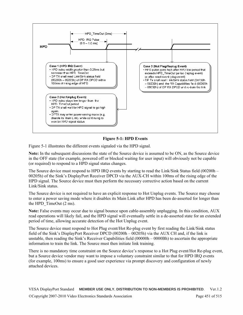
VESA DisplayPort Standard MEMBER USE ONLY. DISTRIBUTION TO NON-MEMBERS IS PROHIBITED. Ver.1.2
©Copyright 2007-2010 Video Electronics Standards Association Page 451 of 515
Figure 5-1: HPD Events
Figure 5-1 illustrates the different events signaled via the HPD signal.
Note: In the subsequent discussions the state of the Source device is assumed to be ON, as the Source device in the OFF state (for example, powered off or blocked waiting for user input) will obviously not be capable (or required) to respond to a HPD signal status changes.
The Source device must respond to HPD IRQ events by starting to read the Link/Sink Status field (00200h – 00205h) of the Sink’s DisplayPort Receiver DPCD via the AUX-CH within 100ms of the rising edge of the HPD signal. The Source device must then perform the necessary corrective action based on the current Link/Sink status.
The Source device is not required to have an explicit response to Hot Unplug events. The Source may choose to enter a power saving mode where it disables its Main Link after HPD has been de-asserted for longer than the HPD_TimeOut (2 ms).
Note: False events may occur due to signal bounce upon cable-assembly unplugging. In this condition, AUX read operations will likely fail, and the HPD signal will eventually settle in a de-asserted state for an extended period of time, allowing accurate detection of the Hot Unplug event.
The Source device must respond to Hot Plug event/Hot Re-plug event by first reading the Link/Sink status field of the Sink’s DisplayPort Receiver DPCD (00200h – 00205h) via the AUX CH and, if the link is unstable, then reading the Sink’s Receiver Capabilities field (00000h – 0000Bh) to ascertain the appropriate information to train the link. The Source must then initiate link training.
There is no mandatory time constraint on the Source device’s response to a Hot Plug event/Hot Re-plug event, but a Source device vendor may want to impose a voluntary constraint similar to that for HPD IRQ events (for example, 100ms) to ensure a good user experience via prompt discovery and configuration of newly attached devices.
VESA DisplayPort Standard MEMBER USE ONLY. DISTRIBUTION TO NON-MEMBERS IS PROHIBITED. Ver.1.2
©Copyright 2007-2010 Video Electronics Standards Association Page 452 of 515
5.1.5 Downstream Device uPacket RX Power Management by a Source Device A Source device must write the value of 2h to DPCD Address 600h of a Sink device via AUX CH in order to place the uPacket RX of a downstream device in a power-save mode. In a power-save mode, the DisplayPort Source device may disable Main Link transmitter for power saving.
The Source device must write the value of 1h to DPCD Address 600h of the downstream device via AUX CH to switch the uPacket RX of the downstream device out of power-save mode. A uPacket RX of a downstream device in a power-save mode may not reply to this AUX request transaction. The uPacket RX of a downstream device in a power-save mode for an open, box-to-box connection is allowed to take up to 1ms till it is ready to reply to the AUX request transaction. Therefore, the Source device must retry until the 1ms wake-up timeout period of the Sink device expires.
Note: For embedded connection, a Sink device may take up to 20ms from a power-save mode till it is ready to reply to AUX request transaction.
Before restarting the Main Link transmission, the Source device must verify that the Sink device replies to an AUX transaction. When restarting the Main Link transmission, the Source device must initiate Link Training first.
The Source device may keep transmitting Idle Pattern over Main Link even when there is no stream to transmit. The Source device may start the transmission of a stream without initiating Link Training. Therefore, the downstream device must keep the Main Link receiver active as long as it is receiving either a stream or Idle Pattern and as long as it keeps the HPD signal asserted.
5.1.6 Source Device Connected to a Branch Device In order to determine whether the Source device is connected to the active protocol converter adaptor, the Source device must read SINK_COUNT at DPCD 00200 Bits5:0. Upon detecting IRQ_HPD pulse, a Source device interfacing with an active protocol converter must check SINK_COUNT to see whether there is a change in the count.
5.2 Sink Device in SST Mode This section describes the requirements for the SST-only mode Sink device for a box-to-box connection.
For embedded connections, it is the responsibility of the system integrator to ensure that the Sink device meets the requirement of a given application.
5.2.1 Stream Sink Requirement This sub-section describes the requirements for the stream Sink in terms of video colorimetry, video timings, and audio formats. A Sink device must describe its capabilities (supported Video Colorimetry Formats, Video Timing Formats and Audio Formats) in the base EDID and/or the CEA-861 Timing Extension Block (optional). The Sink device is required to support EDID Ver.1.4.
5.2.1.1 Video Colorimetry DisplayPort Sink devices support sinking of both RGB, YCbCr, and Y-only colorimetry formats as shown in Table 5-1. Sink devices must read the colorimetry format of the transmitted stream from the DisplayPort Main Stream Attributes.
When receiving a CEA range video stream, the Sink device should anticipate that all the code values may be used by the Source device and clamp the dynamic range if needed.
5.2.1.2 Video Timing Format A DisplayPort Sink device must indicate whether it is able to sink the transmitted video stream by setting or clearing the SINK_STATUS bit of its DPCD.
VESA DisplayPort Standard MEMBER USE ONLY. DISTRIBUTION TO NON-MEMBERS IS PROHIBITED. Ver.1.2
©Copyright 2007-2010 Video Electronics Standards Association Page 453 of 515
All detachable DisplayPort Sink devices must support 640 x 480 @ 60Hz as the fail-safe mode. The Sink is not required to scale 640 x 480 to full screen or center the image, but all pixels are required to be visible.
5.2.1.3 Audio Format A DisplayPort Sink device that outputs audio must support an audio input stream via DisplayPort link. The audio output may be sound waves (speakers) or electrical analog or digital audio output.
Sink Devices that support audio must support stereo 16 bit LPCM at 32kHz, 44.1kHz and 48kHz. It is optional for all audio capable Sink devices to support other sample rates, sample sizes or number of channels.
Sink device must indicate via EDID or the CEA Timing Extension to EDID which audio formats are supported.
Note: As of this writing, only the CEA Timing Extension to EDID provides this information, but it is anticipated that future versions of VESA EDID may also specify audio capabilities of the Sink device, and these would be acceptable to a DisplayPort Source device.
As is the case with sinking video stream, the Sink device must indicate whether it is able to sink the transmitted audio stream by setting or clearing the SINK_STATUS bit of its DPCD.
5.2.2 Sink Device Link Configuration Requirement The Sink device requirement for a supported link configuration depends on whether the device is a “lean-back” display or a “lean-in” display. A lean-back Sink device is a display device that is meant to be viewed from more than 1.2m (approximately 4 feet) away.
A lean-back Sink device must support the number of Main Link lanes that provides for sufficient bandwidth even at a reduced bit rate per lane. This way, the lean-back display device can support a long cable length over which support of only a reduced bit rate is required.
Some examples of lean-back Sink devices are TV displays and projectors. Table 5-2 and Table 5-3 show examples of the required lane counts for these lean-back display devices.
The Sink device of an embedded DisplayPort connection is regarded as a lean-in Sink and is not required to follow the rule of the lean-back Sink described above.
Table 5-2: Required Lane Count for Typical TV Timings at Reduced Bit Rate
Timing Lane Count Remark
Up to 480p/576p @ 50/60Hz One Up to 720p/1080i @ 50/60Hz One @ 50Hz,
Two @ 60Hz One @ 60Hz if 16bpp YCbCr 4:2:2
Up to 1080p @ 50 / 60Hz Four
Table 5-3: Required Lane Count for Typical Data Projector Timings at Reduced Bit Rate
Timing Lane Count Remark
Up to 1024x768 One 18bpp Up to 1680x1050 and 1600x1200
Two 18bpp 18bpp with reduced blanking
Up to 2048x1536 Four 18bpp with reduced blanking
A lean-in display device such as a desktop monitor may choose to minimize the lane count for lowest cost.
For example, a 1400x1050 desktop monitor may have only one Main Link lane.
Note: This example monitor cannot receive its native input resolution over the one lane at the reduced bit rate.
VESA DisplayPort Standard MEMBER USE ONLY. DISTRIBUTION TO NON-MEMBERS IS PROHIBITED. Ver.1.2
©Copyright 2007-2010 Video Electronics Standards Association Page 454 of 515
A Sink device with a captive cable assembly is regarded as a lean-in device, and may choose to minimize the lane count.
5.2.3 Sink Device Behavior on Stream Timing Change
5.2.3.1 Main Video Stream Timing Change As described in Section 5.1.3, the DisplayPort Source device must insert the “idle pattern” (BS + VB-ID + Mvid7:0 +Maud7:0 with NoVideoStream_Flag and VerticalBlanking_Flag (bit 3 and bit 0) of VB-ID both set to 1 every 213 or 8,192 LS_Clk cycles) at least five times before switching to a new video timing. Upon detecting this condition, a Sink device must get ready to receive the new Main Stream Attribute and the main video stream data.
Note: The number of inserted idle patterns may be fewer than five for an embedded DisplayPort connection.
Whether to blank the display during this transition is implementation-specific. Whatever method is selected, showing a visual image that is neither the incoming video stream nor a blank screen should be avoided.
5.2.3.2 Audio Stream Format/Timing Change As for audio format/timing change, the Source device should set and keep VB-ID bit 4 (AudioMute_Flag) to a ‘1’ until after the new Audio InfoFrame and Audio_TimeStamp have been sent. An audio format change is caused by any of:
• A change between the compressed and non-compressed audio
• A change in the sampling rate
• A change in the number of channels
Those packets may be sent as soon as the next frame boundary (when the main video stream is present) or after the next 512th BS symbol set (when the main video stream is absent).
The Sink device must mute the audio when the AudioMute_Flag is set, and should be ready to receive a new audio format upon detecting the change in Audio InfoFrame and Audio_TimeStamp packets.
5.2.4 Toggling of HPD Signal for Status Change Notification When there is a change either in the link status (for example, loss of link synchronization) or the device status (for example, remote control command pending), the Sink device must clear the HPD signal to low for (0.5 ms to 1ms) before setting it to high again, thus generating IRQ_HPD pulse, in order to notify the Source device of the status change.
A Hot Plug event, detected by an upstream DP device as a long HPD pulse (wider than 2ms), prompts the DP Source device to take many actions such as reading of EDID and RX capability in DPCD, and the communication to its operating system. Therefore, a DP Sink device must use IRQ_HPD pulse to notify its upstream device of link status and device status change, instead of generating a long HPD pulse to emulating a Hot Plug event, unless it is prompting the DP Source device to re-read EDID and RX capability. Especially, a DP Sink device must abstain periodic generation of long HPD pulses until the upstream device’s initiating AUX transactions as such actions may lead to soft lock-up condition of a DP Source device.
5.2.5 Sink Device uPacket RX Power-Save Mode A Source device will write the value of 2h to DPCD Address 600h of a Sink device via AUX CH in order to place the uPacket RX of the Sink device in a power-save mode. In a power-save mode, the Sink device may disable Main Link receiver of uPacket RX for power saving.
The Sink device must keep HPD signal asserted unless it is powered off. Therefore, the HPD signal must stay asserted when the Sink device is in a power-save mode.
VESA DisplayPort Standard MEMBER USE ONLY. DISTRIBUTION TO NON-MEMBERS IS PROHIBITED. Ver.1.2
©Copyright 2007-2010 Video Electronics Standards Association Page 455 of 515
When the Sink device receives the AUX request transaction while it is in a power-save mode, the Sink device is not required to reply immediately. However, the Sink device must monitor the presence of differential signal on AUX CH. The Sink device for an open, box-to-box connection must fully enable the AUX CH circuit within 1ms after detection of a differential signal so it can reply to the request transaction retry by Source device.
Note: For an embedded connection, a Sink device may take up to 20ms from a power-save mode until it is ready to reply to an AUX request transaction.
The Source device will write the value of 1h to DPCD Address 600h of the Sink device via AUX CH to switch the Sink device out of power-save mode. Upon this AUX write transaction, the Sink device must be ready for the Source device to initiate Link Training.
The Source device may keep transmitting Idle Pattern over Main Link even when there is no stream to transmit. The Source device may start the transmission of a stream without initiating Link Training. Therefore, the Sink device must keep the Main Link receiver of uPacket RX active as long as it is receiving either a stream or Idle Pattern and as long as it keeps the HPD signal asserted.
The Sink must implement the power state machine shown in Figure 5-2.
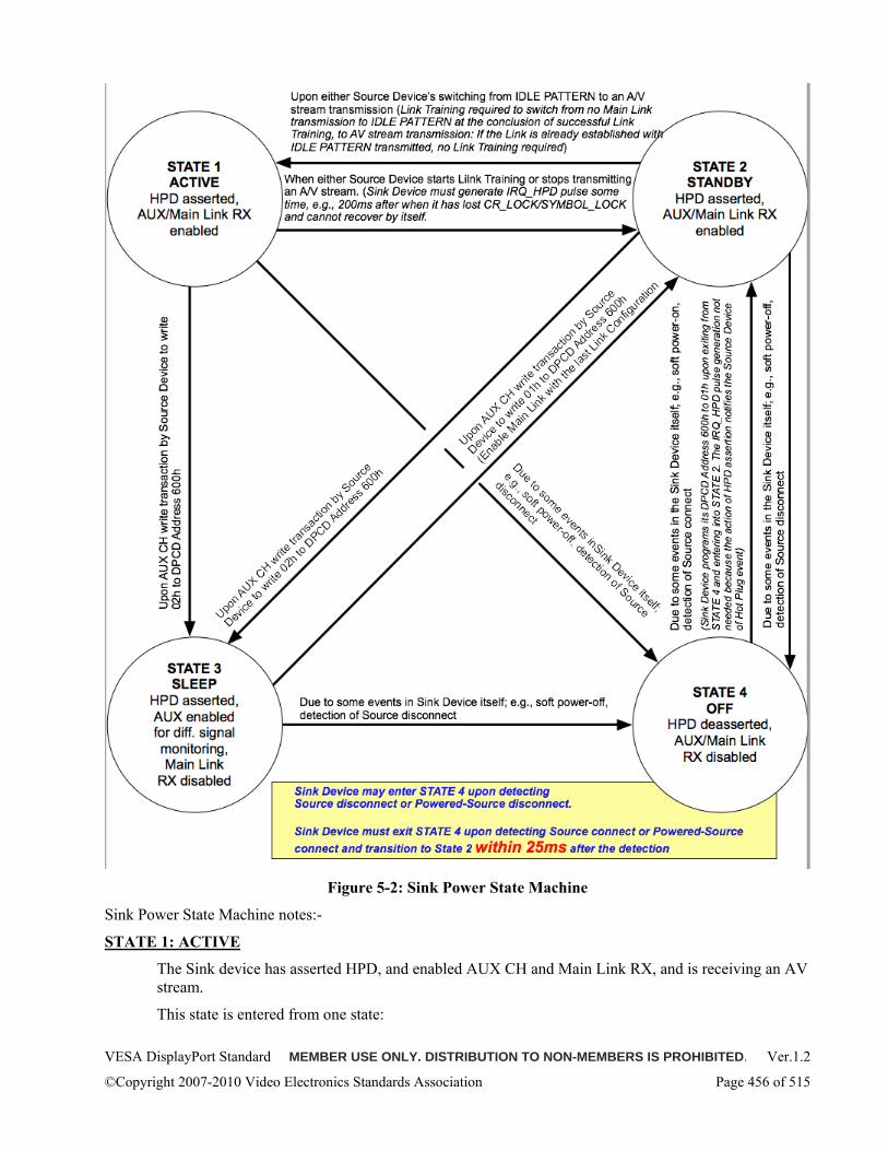
VESA DisplayPort Standard MEMBER USE ONLY. DISTRIBUTION TO NON-MEMBERS IS PROHIBITED. Ver.1.2
©Copyright 2007-2010 Video Electronics Standards Association Page 456 of 515
Figure 5-2: Sink Power State Machine
Sink Power State Machine notes:-
STATE 1: ACTIVE
The Sink device has asserted HPD, and enabled AUX CH and Main Link RX, and is receiving an AV stream.
This state is entered from one state:
VESA DisplayPort Standard MEMBER USE ONLY. DISTRIBUTION TO NON-MEMBERS IS PROHIBITED. Ver.1.2
©Copyright 2007-2010 Video Electronics Standards Association Page 457 of 515
1) From STATE 2 upon either a Source device switching from IDLE PATTERN to an AV stream transmission (Link Training required to switch from no Main Link transmission to IDLE PATTERN at the conclusion of successful Link Training, to AV stream transmission: If the Link is already established with IDLE PATTERN transmitted, no Link Training required)
This state exits to one of three states:
1) To STATE 2 when the Source device either starts Link Training or stops transmitting an AV stream; either transmitting IDLE PATTERN or no Main Link signal at all
2) To STATE 3 AUX write transaction by Source device to write 02h to DPCD Address 600h
3) To STATE 4 due to some events in the Sink device itself; e.g., soft power-off
STATE 2: STANDBY
The Sink device has asserted HPD, and enabled AUX CH and Main Link RX, but is receiving either IDLE PATTERN or no Main Link signal (CR_LOCK and SYMBOL_LOCK both lost)
This state is entered from one of three states:
1) From STATE 4 due to some events in the Sink device itself; e.g., soft power-on (Sink device programs its DPCD Address 600h to 01h upon exiting from STATE 4 and entering into STATE 2. The IRQ_HPD pulse generation is not needed because the action of HPD assertion notifies the Source device of Hot Plug event)
2) From STATE 3 upon AUX write transaction by the Source device to write 01h to DPCD Address 600h
3) From STATE 1 when the Source device stops transmitting an AV stream (Sink device must generate IRQ_HPD pulse sometime (e.g., 200ms) after it has stopped receiving Main Link signal, that is, neither AV stream nor IDLE PATTERN)
This state exits to one of three states:
1) To STATE 4 due to some events in the Sink device itself; e.g., soft power-off
2) To STATE 3 upon AUX write transaction by the Source device to write 02h to DPCD Address 600h
3) To STATE 1 upon either Source device’s switching from IDLE PATTERN to an AV stream transmission (Link Training required to switch from no Main Link transmission to IDLE PATTERN at the conclusion of successful Link Training, to AV stream transmission: If the Link is already established with IDLE PATTERN transmitted, no Link Training required)
STATE 3: SLEEP
The Sink device has asserted HPD, and enabled AUX CH enough to at least monitor incoming AUX CH differential signals. Main Link RX disabled
This state is entered from one of two states: 1) From STATE 2 upon AUX write transaction by the Source device to write 02h to DPCD Address 600h
2) From STATE 1 upon AUX write transaction by the Source device to write 02h to DPCD Address 600h
This state exits to one of two states: 1) To STATE 4 due to some events in the Sink device itself; e.g., soft power-off
VESA DisplayPort Standard MEMBER USE ONLY. DISTRIBUTION TO NON-MEMBERS IS PROHIBITED. Ver.1.2
©Copyright 2007-2010 Video Electronics Standards Association Page 458 of 515
2) To STATE 2 upon AUX write transaction by the Source device to write 01h to DPCD Address 600h
STATE 4: OFF
The Sink device has de-asserted HPD, and disabled AUX CH/Main Link
This state is entered from one of three states: 1) To STATE 3 due to some events in the Sink device itself; e.g., soft power-off
2) To STATE 2 due to some events in the Sink device itself; e.g., soft power-off
3) To STATE 1 due to some events in the Sink device itself; e.g., soft power-off (the Sink device may enter this state upon detecting Source disconnect or Powered-Source disconnect)
This state exits to one state: 1) To STATE 2 due to some events in the Sink device itself; e.g., soft power-on (the Sink device may exit this state upon detecting Source connect or Powered-Source connect)
5.3 Branch Device in SST-only Mode This section describes the requirement for SST-only mode DisplayPort Branch devices. Branch device types are summarized in this section.
5.3.1 EDID Access Handling Requirement Branch device must make sure that the stream transmitted by the Source device can be sunk by at least one Sink device in the link. Therefore, a Branch device without its own local sink must forward the EDID access request from its upstream device to its downstream device.
When a Branch device has multiple downstream ports, it has multiple choices regarding which downstream device(s) should receive the EDID access request.
The DP Branch device must route the EDID access to the lowest numbered, unassigned, downstream port to which a downstream device is connected. If the DP Branch device is a matrix switch with multiple input and output ports capable of multiple connections (for example, Input Port N to Output Port M, Input Port N+1 to Output Port M+1), then the subsequent SST Source devices connected must be assigned the lowest numbered, unassigned, connected downstream port among the remaining ones. If there is no unassigned, connected downstream port, the Branch device must wait until a downstream port becomes connected or another SST DP Source device is disconnected before assigning a port to the SST DP Source device.
5.3.2 Branch Device Link Configuration Requirements DP Branch devices must support four Main Link lanes both for receive and downstream ports. When an upstream device configures the link to an SST-only mode DP Branch device, the DP Branch device must configure its downstream link to the same link configuration (in terms of lane count and bit rate) as the upstream link.
Once both the upstream and downstream links are configured, DP Branch device repeaters must transport all DisplayPort control and data stream symbols from input to output. Table 5-4 below lists all the DPCD parameters a Branch device may update depending on the capability of its downstream links.
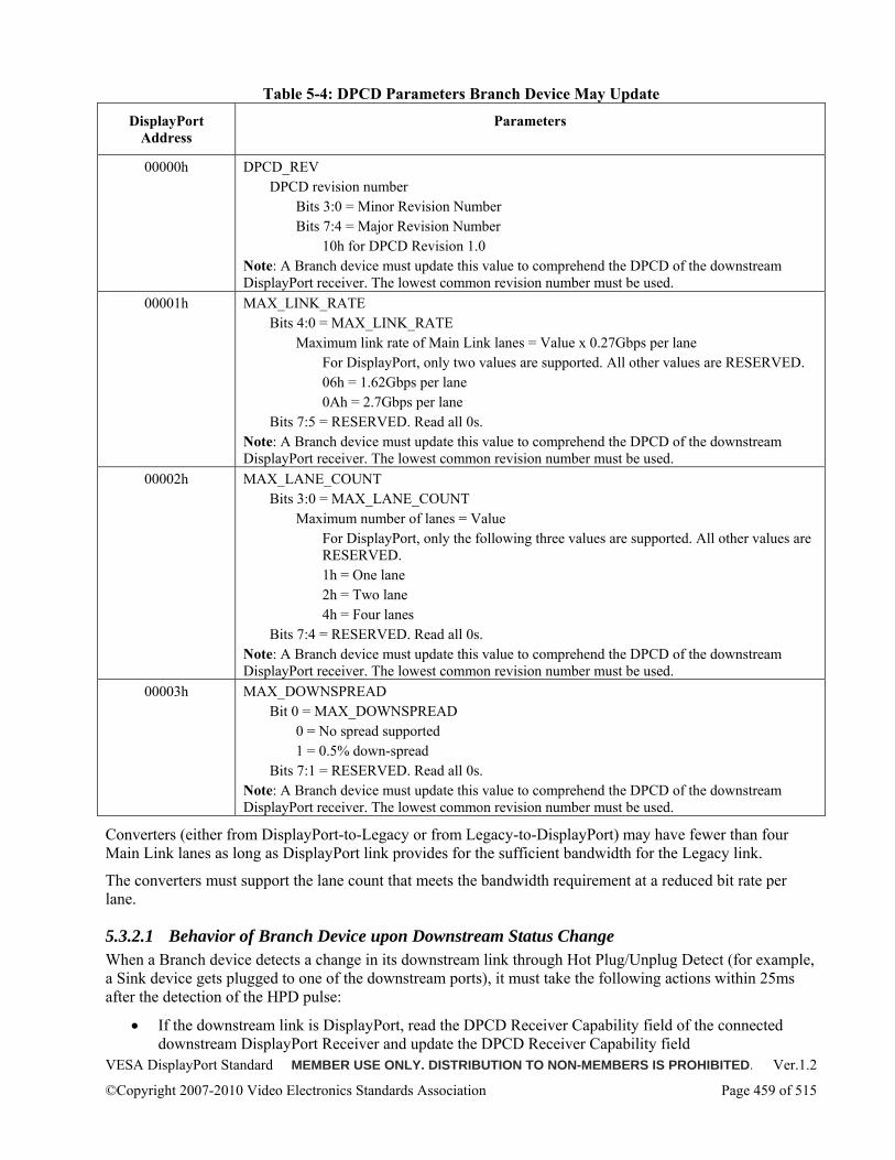
VESA DisplayPort Standard MEMBER USE ONLY. DISTRIBUTION TO NON-MEMBERS IS PROHIBITED. Ver.1.2
©Copyright 2007-2010 Video Electronics Standards Association Page 459 of 515
Table 5-4: DPCD Parameters Branch Device May Update
DisplayPort Address
Parameters
00000h DPCD_REV DPCD revision number
Bits 3:0 = Minor Revision Number Bits 7:4 = Major Revision Number
10h for DPCD Revision 1.0 Note: A Branch device must update this value to comprehend the DPCD of the downstream DisplayPort receiver. The lowest common revision number must be used.
00001h MAX_LINK_RATE Bits 4:0 = MAX_LINK_RATE
Maximum link rate of Main Link lanes = Value x 0.27Gbps per lane For DisplayPort, only two values are supported. All other values are RESERVED. 06h = 1.62Gbps per lane 0Ah = 2.7Gbps per lane
Bits 7:5 = RESERVED. Read all 0s. Note: A Branch device must update this value to comprehend the DPCD of the downstream DisplayPort receiver. The lowest common revision number must be used.
00002h MAX_LANE_COUNT Bits 3:0 = MAX_LANE_COUNT
Maximum number of lanes = Value For DisplayPort, only the following three values are supported. All other values are RESERVED. 1h = One lane 2h = Two lane 4h = Four lanes
Bits 7:4 = RESERVED. Read all 0s. Note: A Branch device must update this value to comprehend the DPCD of the downstream DisplayPort receiver. The lowest common revision number must be used.
00003h MAX_DOWNSPREAD Bit 0 = MAX_DOWNSPREAD
0 = No spread supported 1 = 0.5% down-spread
Bits 7:1 = RESERVED. Read all 0s. Note: A Branch device must update this value to comprehend the DPCD of the downstream DisplayPort receiver. The lowest common revision number must be used.
Converters (either from DisplayPort-to-Legacy or from Legacy-to-DisplayPort) may have fewer than four Main Link lanes as long as DisplayPort link provides for the sufficient bandwidth for the Legacy link.
The converters must support the lane count that meets the bandwidth requirement at a reduced bit rate per lane.
5.3.2.1 Behavior of Branch Device upon Downstream Status Change When a Branch device detects a change in its downstream link through Hot Plug/Unplug Detect (for example, a Sink device gets plugged to one of the downstream ports), it must take the following actions within 25ms after the detection of the HPD pulse:
• If the downstream link is DisplayPort, read the DPCD Receiver Capability field of the connected downstream DisplayPort Receiver and update the DPCD Receiver Capability field
VESA DisplayPort Standard MEMBER USE ONLY. DISTRIBUTION TO NON-MEMBERS IS PROHIBITED. Ver.1.2
©Copyright 2007-2010 Video Electronics Standards Association Page 460 of 515
(MAX_LINK_RATE, MAX_LANE_COUNT, etc.) to comprehend the capability of the downstream DisplayPort Receiver.
• Increase the SINK_COUNT value as follows:
o If the immediate downstream link is DisplayPort, increase the SINK_COUNT value by the SINK_COUNT value of the immediate downstream device.
o If the immediate downstream link is Legacy, increase the SINK_COUNT by 1 when the downstream link is detected “loaded.”
Note: If the immediate downstream is Legacy without “loaded” detection, always assume the Sink is connected.
After the action above, Branch device must de-assert the HPD signal of its upstream port within 25ms. The HPD pulse width must be set as follows:
• Long HPD pulse (wider than 2ms, emulating Hot Plug event) when the Branch device has changed its receiver capability field to match that of a newly plugged downstream device.
• IRQ_HPD pulse when forwarding the Device Service IRQ vector, notifying SINK_COUNT value change (including the unplug of the downstream device).
When the Branch device generates a Hot Plug event pulse to its upstream port, it must wait for the upstream link to be trained, and then train the downstream link.
Note: HDCP Version 1.3 Amendment for DisplayPort Revision 1.1 has added a mechanism allowing a SST-only mode Branch device to notify the Hot Plug/Unplug of a downstream device via IRQ_HPD, instead of Hot Plug event pulse (wider than 2ms), when an upstream device sets Hot Plug event/Hot Unplug Event Notification Type bit (bit 0 of BRANCH_DEVICE_CTRL field at DPCD Address 001A1h) to 1.
The Branch device HPD propagation latency requirement of within 50 ms (25ms for downstream and 25ms for upstream) must apply even when it is an HDCP-enabled Branch device with DPCD Revision number of 1.2 or higher (and thus, supporting BRANCH_DEVICE_CTRL field at DPCD Address 001A1h).
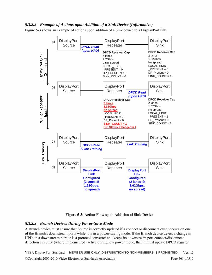
VESA DisplayPort Standard MEMBER USE ONLY. DISTRIBUTION TO NON-MEMBERS IS PROHIBITED. Ver.1.2
©Copyright 2007-2010 Video Electronics Standards Association Page 461 of 515
5.3.2.2 Example of Actions upon Addition of a Sink Device (Informative) Figure 5-3 shows an example of actions upon addition of a Sink device to a DisplayPort link.
DPCD Receiver Cap2 lanes1.62GbpsNo spreadLOCAL_EDID_PRESENT = 0DP_Present = 0SINK_COUNT = 1DP_Status_Changed = 1
DPCD Receiver Cap4 lanes2.7Gbps0.5% spreadLOCAL_EDID_PRESENT = 0DP_PRESETN = 1SINK_COUNT = 0
DisplayPort Repeater
DisplayPortSink
DPCD Receiver Cap2 lanes1.62GbpsNo spreadLOCAL_EDID_PRESENT = 0DP_Present = 0SINK_COUNT = 1
DisplayPortRepeater
DisplayPortSinkDPCD Read
(upon HPD)
DisplayPort Source
DisplayPort Repeater
DisplayPort Sink
DisplayPort Link
Configured(2 lanes @ 1.62Gbps,no spread)
DisplayPort Link
Configured(2 lanes @ 1.62Gbps,no spread)
a)
b)
c)
DPCD Read (upon HPD)
DPCD Receiver Cap2 lanes1.62GbpsNo spreadLOCAL_EDID_PRESENT = 1DP_Present = 0SINK_COUNT = 1
DisplayPortSource
DisplayPort Repeater
DisplayPort Sink
DPCD Read / Link Training
Link Training
d)
DisplayPort Source
DisplayPortSource
Figure 5-3: Action Flow upon Addition of Sink Device
5.3.2.3 Branch Devices During Power-Save Mode A Branch device must ensure that Source is correctly updated if a connect or disconnect event occurs on one of the Branch's downstream ports while it is in a power-saving mode. If the Branch device detect a change in HPD on a downstream port or is a protocol converter and keeps its downstream port connect/disconnect detection circuitry (where implemented) active during low power mode, then it must update DPCD register
VESA DisplayPort Standard MEMBER USE ONLY. DISTRIBUTION TO NON-MEMBERS IS PROHIBITED. Ver.1.2
©Copyright 2007-2010 Video Electronics Standards Association Page 462 of 515
00200h and issue an interrupt (HPD_IRQ) whenever it detects a connect/disconnect event on a downstream port.
Note: The Source can decide whether to ignore the interrupt or to bring the Branch device out of low power in order to read the new value in DPCD register 00200h. The Branch device must not exit low power mode when it detects connect/disconnect. If the Branch device has downstream connect/disconnect detection circuitry but disables it during low power mode or disables its HPD detection circuitry during power-save mode (as appropriate), then the Branch device must preserve the sense of the connected display during sleep, and on exit from low power mode the Branch device must reactivate its downstream port connect/disconnect detection or HPD detection circuitry, update DPCD register 00200h only if necessary, and generate an HPD_IRQ interrupt if the result of this update is to change the preserved value stored in DPCD register 00200h.
5.4 Source Device in MST Mode An MST Source device first checks whether the downstream device has DPCD Revision number of 1.2 or higher and whether MST_CAP bit is set. When the downstream device has MST_CAP bit set, the MST Source device indicates to the downstream device that it is a Source device by setting UPSTREAM_IS_SRC bit and that it is an MST device by setting UP_REQ_EN bit (both in MSTM_CTRL field at DPCD Address 00111h). The MST Source device must not set/clear UP_REQ_EN bit while transmitting active stream. In other words, the uPacket TX must be either disabled/parked to the termination voltage or transmitting IDLE_PATTERN in SST-only mode and empty MTPs in MST mode when the MST Source device changes the UP_REQ_EN bit of the downstream device via Native AUX WR transaction.
The MST Source device must not set/clear MST_EN bit while transmitting active stream. Furthermore, it must set UP_REQ_EN bit before setting MST_EN bit.
The MST Source device operates in the following ways depending on how it sets UP_REQ_EN and MST_EN bits.
Table 5-5: UP_REQ_EN/MST_EN Setting
UP_REQ_EN /MST_EN
Operation
0 / 0 Acts and is treated as an SST-only mode Source device. A downstream Branch device, even if it is an MST Branch device, forwards the incoming SST transport format from this Source device to the downstream device in SST transport format, configuring its downstream link the same way as the upstream link as described in Section 5.3.2.. If the downstream Branch device is SST-only mode, then the Source device must use this bit combination.
0 / 1 Invalid setting. MST transport format will not be forwarded by the downstream Branch device because the MST transport requires the virtual channel be established by Topology Manager and Source Payload Bandwidth Manger prior to the transmission, and because the Source device cannot play the role of Topology Manager and Source Payload Bandwidth Manager unless it sets UP_REQ_EN bit to 1.
1 / 0 MST Source device choosing to transmit in SST transport format. The MST Source device plays the role of Topology Manager and Source Payload Bandwidth Manager and establishes the virtual channel by originating ALLOCATE_PAYLOAD message transaction prior to SST transport format transmission. The downstream MST Branch device (it is an MST Branch device as the Source device sets UP_REQ_EN bit to 1 only after confirming that its downstream device has MST_CAP bit set to 1) converts the incoming SST transport format into MST transport format and forwards to the downstream port specified via ALLOCATE_PAYLOAD message transaction.
1 / 1 MST Source device transmitting in MST transport format. The downstream MST Branch device forwards the incoming MST transport format to the downstream port in a pass-through manner as described in Section 2.6.
VESA DisplayPort Standard MEMBER USE ONLY. DISTRIBUTION TO NON-MEMBERS IS PROHIBITED. Ver.1.2
©Copyright 2007-2010 Video Electronics Standards Association Page 463 of 515
The MST Source device transmitting in MST transport format may choose any link configuration that provides for sufficient link bandwidth for the stream transmits. It should be noted that changing of the link configuration and switching from SST to MST results in the interruption of the transport of a stream.
An MST Source device must read the ESI field at 02002h ~ 0200Fh when it receives an IRQ_HPD pulse in stead of the Sink Status field (00200h region) as the ESI field allows all the necessary Device and Link status information including RX capability change and Link Status change in a single Native AUX RD transaction.
5.5 Sink Device in MST Mode An MST Sink device must support both SST format and MST format. Even when the MST Sink device sets MST_CAP bit to 1, a Source device directly driving the Sink device may transmit either in SST transport format or MST transport format.
If an MST Sink device desires to receive a stream in SST format, it must clear the MST_CAP bit. When the MST Sink device changes the MST_CAP bit (either 0 to 1 or 1 to 0) while an upstream device stays connected, the MST Sink device must generate an IRQ_HPD after having set RX_CAP_CHANGED bit in LINK_SERVICE_IRQ_ESI0 field at DPCD Address 02008h.
When the MST Sink device clears MST_CAP bit, this status change is forwarded to the upstream Source devices via CONNECTION_STATUS_NOTIFY broadcast message transaction. The Source device might have originated a message transaction targeted at this MST Sink device by the time it received the broadcast message transaction. In this case, the MST Sink device that has cleared the MST_CAP bit must not reply to the received message transaction. The MST Sink device must not originate broadcast message transaction after it has cleared the MST_CAP bit.
5.6 Branch Device in MST Mode An MST Branch device must set the MST_CAP bit of its upstream uPacket RX port, and set UP_REQ_EN bit and enable the MST transport format of its downstream uPacket TX as long as its downstream device is MST-capable (MST_CAP bit = 1). As described in Section 5.4, the MST Branch device must not set UP_REQ_EN and MST_EN bits while forwarding active stream. Furthermore, the MST Branch device must set UP_REQ_EN bit before setting MST_EN bit.
The MST Branch device must support four lanes both on the upstream uPacket RX port and the downstream uPacket TX port, and must always set the downstream link configuration to the maximum link bandwidth in order to avoid the interruption of stream transport due to the link configuration change.
When an SST-only mode Source device is connected to an MST Branch device, the MST Branch device must first stop forwarding active stream, clear MST_EN bit, and then clear UP_REQ_EN to act as an SST-only mode Branch device. As an SST-only mode Branch device, the Branch device configures the lowest numbered, unassigned, connected downstream link the same way as the upstream link to which an SST-only mode Source device is connected and forward the incoming SST transport format to the downstream link in an SST transport format as described in Section 5.3.2.
As stated in Section 5.3.2., the Branch device must generate a long HPD pulse when it has changed its receiver capability field to match that of a newly plugged downstream device.
5.7 Cable-Connector Assembly This section describes the requirement for the cable-connector assembly.
5.7.1 Box-to-Box, End-User-Detachable Cable Assembly A box-to-box, detachable DisplayPort cable assembly must support four Main Link lanes.
VESA DisplayPort Standard MEMBER USE ONLY. DISTRIBUTION TO NON-MEMBERS IS PROHIBITED. Ver.1.2
©Copyright 2007-2010 Video Electronics Standards Association Page 464 of 515
Box-to-box, detachable DisplayPort cable assemblies of two meters or less must meet the high bit rate cable specification detailed in Section 4.
All box-to-box, detachable DisplayPort cable assemblies must meet the low bit rate cable specification as detailed in Section 4.
The mating connectors of the box-to-box DisplayPort connection must meet the connector specification as detailed in Section 4.
5.7.2 Embedded and Captive Cable Assembly An embedded or captive DisplayPort cable assembly may support fewer than four Main Link lanes as long as “sufficient” link bandwidth is provided for the design application with fewer lanes.
For embedded and captive connections, it is the responsibility of the system integrator to select the cable assembly with sufficient bandwidth capacity.
VESA DisplayPort Standard MEMBER USE ONLY. DISTRIBUTION TO NON-MEMBERS IS PROHIBITED. Ver.1.2
©Copyright 2007-2010 Video Electronics Standards Association Page 465 of 515
6 Appendix A: Audio Transport (Informative) Audio-related secondary-data packets are covered in Section 2.2.5. This appendix, intended to be read along with that section, aims to add clarification to the Standard and to reduce ambiguity in order to improve the interoperability between audio-capable DP devices.
6.1 Audio Stream Components An audio stream consists of following components: Audio Stream Packets, Audio Time-stamp Packets; Audio Info Packets (as defined in CEA861-C Specification) and some portion of VB-ID. In DisplayPort Standards, all audio-related packets except VB-ID are transported as part of the secondary-data packet stream.
An Audio Stream Packet includes audio stream itself and some attribute information such as audio coding type and channel count. Depending on the coding type of Audio Stream Packet, it may contain status information about parameters of the audio stream. For example, the existing format, which is similar to IEC60958 standard, transfers this information in serial format via block of samples. (Refer to IEC60958-1 and IEC60958-3 standards).
An Audio InfoFrame Packet is used for transferring attributes of the audio stream in a separate packet. Depending on the coding type of the Audio Stream Packet, there is some overlap between the information carried by Audio Stream Packet and that carried by Audio Info Frame Packet. Whenever there is an overlap, the information carried by the Audio Stream Packet takes precedence. As a matter of fact, the Audio InfoFrame Packet must be referred to only for audio channel to speaker mapping in the DisplayPort Standard. When one or two channel audio is transported, the CEA861-C Specification defines only a single channel to speaker mapping. Therefore, the transmission of an Audio InfoFrame may be omitted altogether.
An Audio Time-stamp Packet is used for the audio clock regeneration to restore the audio master clock frequency needed for further audio processing.
Additional signals such as “audio mute” signal for disabling audio are carried in the VB-ID byte transmitted next to each BS control symbol.
Section 6.2 describes how the time slot for Audio Stream Packet transmission must be scheduled. As far as the Audio Time-stamp Packet and Audio InfoFrame Packet are concerned, they must be transmitted once per frame. It is recommended that they be transmitted during the main video stream vertical blanking period.
Note: The Audio Time-stamp Packet may be transferred more than once per frame. It is up to each DP transmitter implementation to decide how many times to transfer the Audio Time-stamp Packet.
6.2 Association of Three Packet Types via Packet ID The transport of an audio stream over a DP link involves transmission of three packet types: Audio Stream Packet, Audio Time-stamp Packet, and Audio InfoFrame Packet. These three types of packets for a single audio stream are associated with one another by having the same Secondary-data Packet ID (00h) carried as HB0 (header byte 0) of each packet.
6.3 Scheduling of Audio Stream Packet Transmission An audio stream is a continuous (that is, isochronous) stream of audio samples, each of which may contain several channels of audio signals at a pre-defined sample frequency (fs). The sample frequency is typically in the range of 32kHz to 192kHz.
The transmission scheduler for an Audio Stream Packet must wait for a time slot for audio transmission during which there are no main video stream, Main Stream Attribute Packet, and other higher priority secondary-data packets in queue. Therefore, the DP transmitter and receiver are required to have some buffer space to hold the audio data while the Audio Stream Packet is waiting for its time slot.
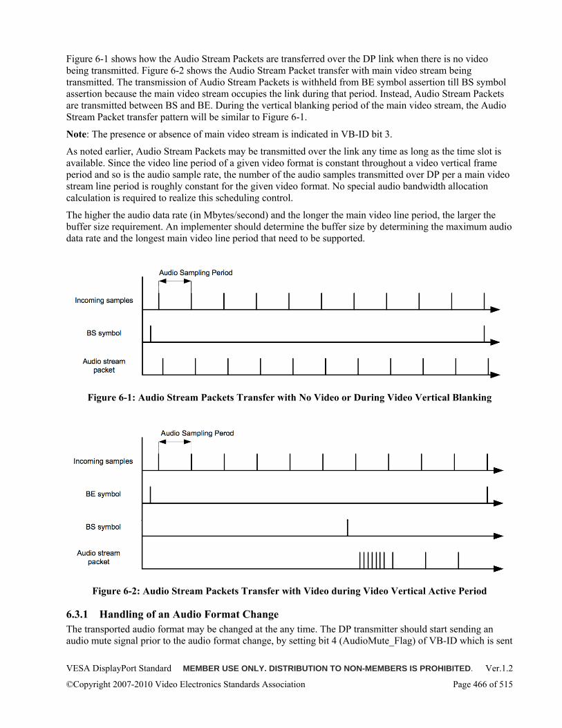
VESA DisplayPort Standard MEMBER USE ONLY. DISTRIBUTION TO NON-MEMBERS IS PROHIBITED. Ver.1.2
©Copyright 2007-2010 Video Electronics Standards Association Page 466 of 515
Figure 6-1 shows how the Audio Stream Packets are transferred over the DP link when there is no video being transmitted. Figure 6-2 shows the Audio Stream Packet transfer with main video stream being transmitted. The transmission of Audio Stream Packets is withheld from BE symbol assertion till BS symbol assertion because the main video stream occupies the link during that period. Instead, Audio Stream Packets are transmitted between BS and BE. During the vertical blanking period of the main video stream, the Audio Stream Packet transfer pattern will be similar to Figure 6-1.
Note: The presence or absence of main video stream is indicated in VB-ID bit 3.
As noted earlier, Audio Stream Packets may be transmitted over the link any time as long as the time slot is available. Since the video line period of a given video format is constant throughout a video vertical frame period and so is the audio sample rate, the number of the audio samples transmitted over DP per a main video stream line period is roughly constant for the given video format. No special audio bandwidth allocation calculation is required to realize this scheduling control.
The higher the audio data rate (in Mbytes/second) and the longer the main video line period, the larger the buffer size requirement. An implementer should determine the buffer size by determining the maximum audio data rate and the longest main video line period that need to be supported.
Figure 6-1: Audio Stream Packets Transfer with No Video or During Video Vertical Blanking
Figure 6-2: Audio Stream Packets Transfer with Video during Video Vertical Active Period
6.3.1 Handling of an Audio Format Change The transported audio format may be changed at the any time. The DP transmitter should start sending an audio mute signal prior to the audio format change, by setting bit 4 (AudioMute_Flag) of VB-ID which is sent
VESA DisplayPort Standard MEMBER USE ONLY. DISTRIBUTION TO NON-MEMBERS IS PROHIBITED. Ver.1.2
©Copyright 2007-2010 Video Electronics Standards Association Page 467 of 515
once per main video stream line period (or once per 8192 link symbols when the main video stream is absent). An audio format change is caused by any of:
• A change between the compressed and non-compressed audio
• A change in the sampling rate
• A change in the number of channels
This signal indicates to the DP receiver that the audio system is in a transient process and the audio stream may be not valid at this time. When the AudioMute_Flag is ‘1’, a DP receiver must disable its audio output while continuing to receive and process Audio Time-stamps.
The DP transmitter should clear the AudioMute_Flag to ‘0’ only after finishing the transient process at the audio source input, finishing audio clock measurement with a correct and stable value and providing information about this change to the receiver. The DP transmitter should clear the audio mute signal only after transferring Audio Time-stamp and Audio Info packet (if needed).
Once the DP transmitter clears the AudioMute_Flag to ‘0’, a DP receiver should enable its audio output only after the regenerated audio clock becomes stable and after it has collected enough audio status information.
6.4 Structure of Audio Stream Packet This Standard defines only one audio coding type which is similar to IEC 60958 format, as specified in bits 7:4 of HB3 (header byte 3). However, other coding types are expected to be added in the future. Therefore, a DP receiver must check the coding type field to remain compatible with future versions/revisions of this Standard.
ChannelCount field (bits 2:0 of header byte 3 (HB3)) carries information about the count of audio channels transmitted over the link. This field must have following values: 000 for one channel audio, 001 for two channel audio, up to 111 for eight channel audio.
The audio stream payload data structure has two configurations: One is for one- or two-channel audio and the other for three- to eight-channel audio. An Audio Stream Packet may have variable payload size. At the minimum, Audio Stream Packet size is as follows:
6.4.1 One or Two Channel Audio Four header bytes protected by four ECC parity bytes, followed by 16 payload data bytes protected by four ECC parity bytes. The 16 payload data bytes consist of four 32 bit audio channel samples. Each of the 16 payload data bytes carries two audio samples, each consisting of 1st channel and 2nd channel audio samples. For one channel audio, the 2nd channel audio sample data must be zero padded.
6.4.2 Three to Eight Channel Audio Four header bytes protected by four ECC parity bytes, followed by two sets of 16 payload data bytes, each protected by four ECC parity bytes (resulting in 32 data bytes plus 8 ECC parity bytes). As is the case with one or two channel audio, each of the 16 payload data bytes consists of four 32 bit audio samples. When the channel count is less than eight, unused audio channel sample data must be zero padded.
The DP transmitter may use one common Audio Stream packet size for both one and two channel audio and three to eight channel audio modes. In this case, the packet payload configuration consisting of 32 data bytes plus 8 ECC parity bytes (the payload configuration for three to eight channel audio described in the previous paragraph) must be used.
The DP transmitter may concatenate multiple sets of minimum packet payload to form a long packet that has up to 256 data bytes for one or two channel audio and 1024 data bytes in case of three to eight channel audio.
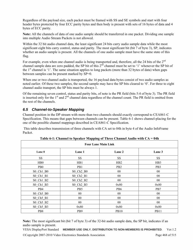
VESA DisplayPort Standard MEMBER USE ONLY. DISTRIBUTION TO NON-MEMBERS IS PROHIBITED. Ver.1.2
©Copyright 2007-2010 Video Electronics Standards Association Page 468 of 515
Regardless of the payload size, each packet must be framed with SS and SE symbols and start with four header bytes protected by four ECC parity bytes and then body is present with sets of 16 bytes of data and 4 bytes of ECC parity.
Note: All the channels of data of one audio sample should be transferred in one packet. Dividing one sample into multiple Audio Stream Packets is not allowed.
Within the 32 bit audio channel data, the least significant 24 bits carry audio sample data while the most significant eight bits carry control, status and parity. The most significant bit (bit 7 of byte 3), SP, indicates whether an audio sample is present. All the channels of one audio sample must have the same state of this flag.
For example, even when one channel audio is being transported and, therefore, all the 24 bits of the 2nd channel sample data are zero padded, the SP bit of this 2nd channel must be set to ‘1’ whenever the SP bit of the 1st channel is ‘1’. The same situation applies to long packets (more than 32 bytes of data) when gaps between samples can be present marked by SP=0.
When one or two channel audio is transported, the 16 payload data bytes consist of two audio samples as noted earlier. Of these two samples, the second sample may have the SP bits cleared to ‘0’. For three to eight channel audio transport, the SP bits must be always 1.
Of the remaining seven control, status and parity bits, of note is the PR field (bits 5:4 of byte 3). The PR field is inserted only for the 1st and 2nd channel data regardless of the channel count. The PR field is omitted from the rest of the channels.
6.5 Channel-to-Speaker Mapping Channel position in the DP stream with more than two channels should exactly correspond to CEA861-C Specification. This means that gaps between channels can be present. Table 6-1 shows channel-placing for the one of the possible channel mappings described in CEA861-C Specification.
This table describes transmission of three channels with CA set to 04h in byte 4 of the Audio InfoFrame Packet.
Table 6-1: Channel to Speaker Mapping of Three Channel Audio with CA = 04h
Four Lane Main Link
Lane 0 Lane 1 Lane 2 Lane 3
SS SS SS SS HB0 HB1 HB2 HB3 PB0 PB1 PB2 PB3
S0_Ch1_B0 S0_Ch2_B0 00 00 S0_Ch1_B1 S0_Ch2_B1 00 00 S0_Ch1_B2 S0_Ch2_B2 00 00 S0_Ch1_B3 S0_Ch2_B3 0x80 0x80
PB4 PB5 PB6 PB7 S0_Ch5_B0 00 00 00 S0_Ch5_B1 00 00 00 S0_Ch5_B2 00 00 00 S0_Ch5_B3 0x80 0x80 0x80
PB8 PB9 PB10 PB11
Note: The most significant bit (bit 7 of byte 3) of the 32-bit audio sample data, the SP bit, indicates if an audio sample is present.
VESA DisplayPort Standard MEMBER USE ONLY. DISTRIBUTION TO NON-MEMBERS IS PROHIBITED. Ver.1.2
©Copyright 2007-2010 Video Electronics Standards Association Page 469 of 515
The channel to speaker mapping information is provided in an Audio InfoFrame Packet as described in Table 20 of the CEA861-C Specification. When one-channel audio is transported, it must use the FL channel (that is, Channel 1).
6.6 Transfer of Sample Frequency Information Information about audio sampling frequency is transferred in an Audio Time-stamp Packet, which provides the audio clock frequency information (Maud and Naud) using the following formula:
• Maud / Naud = 512 * fs / f_LS_Clk
where fs is the sampling frequency of the audio stream being transported.
In accordance with the DisplayPort Standard, this information is transferred at least once per video frame (or following 512th BS symbol when the main video stream is not present). A DP transmitter is allowed to transmit it more frequently if it chooses to do so. In addition, the Standard allows for the transmission of the least significant eight bits of the Maud value once per line of main video stream line and it is up to the DP receiver to use or not this information.
How a DP receiver regenerates the audio sampling frequency is implementation specific and is beyond the scope of this Standard.
For example: Some implementations may use the Maud and Naud values to set the initial frequency of the audio clock recovery circuit and perform the fine frequency adjustment based on the audio FIFO fill rate. With this method, a DP receiver may ignore Maud7:0 data from the VB-ID packet.
VESA DisplayPort Standard MEMBER USE ONLY. DISTRIBUTION TO NON-MEMBERS IS PROHIBITED. Ver.1.2
©Copyright 2007-2010 Video Electronics Standards Association Page 470 of 515
7 Appendix B: Sink Event Notification Example (Informative) This appendix describes a mechanism through which the SST-mode-only DisplayPort Sink device can notify the DisplayPort Source device of a Sink event such as a display orientation switch between portrait and landscape. An MST Sink device connected to an MST upstream device must notify a Sink event via SINK_EVENT_NOTIFY broadcast message transaction.
7.1 Mutual Identification by Source and Sink Upon a Hot-Plug Event, the Source device and Sink device may identify each other by accessing the Source-specific field (Address 300h to 3FFh) and Sink-specific field (400h to 4FFh) of the DPCD. A Source device that is interested in enabling its “Extension” feature should write its own 24 bit IEEE OUI (Organizational Unique ID) to Addresses 300h to 302h and read the 24 bit IEE OUI of the Sink device from Addresses 400h to 402h. The Source device may optionally write and read more than 3 bytes of IEEE OUI to exchange further identification information (for example, Chip ID and Revision ID). The “Extension” feature is enabled only when each device recognizes that the other device supports it.
7.2 IRQ_HPD Pulse and Sink-Specific IRQ A Sink device that supports the Sink event notification feature indicates what Sink event types are supporting by setting “Sink_Event_Type” byte(s) in the sink specific field. The Source device, upon reading the Sink_Event_Type byte(s) via the AUX CH, enables certain Sink events by writing to the Sink_Event_Mask byte(s) in the Sink specific field. The address mapping of Sink_Event_Type byte(s) and Sink_Event_Mask byte(s) is implementation-specific.
When the selected Sink event (such as the display orientation switch) occurs, the Sink device takes the following actions:
• Programs a set of parameters to a pre-defined address range of the Sink-specific field
• Sets Sink-specific IRQ bit of DPCD (Bit 6 of Address 201h)
• Generates IRQ_HPD pulse on the HPD signal line
The Source device, upon detecting the IRQ_HPD pulse, takes the following actions:
• Reads the Link/Sink Status field of DPCD and identifies that the cause of IRQ is Sink-specific
• Reads a set of parameters from the pre-defined address range of the Sink-specific field
• Performs an operation according to the read parameters:
o If the notified Sink event is a display orientation change, it may change the orientation of the video data it is transmitting.
VESA DisplayPort Standard MEMBER USE ONLY. DISTRIBUTION TO NON-MEMBERS IS PROHIBITED. Ver.1.2
©Copyright 2007-2010 Video Electronics Standards Association Page 471 of 515
8 Appendix C: Link Quality Management (Informative) This appendix provides guidelines for ensuring link quality, with the goal of providing minimal disruption during normal operation.
8.1 Marginal Link Quality The link training procedure necessarily does not take sufficient time to be able to perform a full link quality analysis. The consequence is that a connection between a DisplayPort transmitter and a DisplayPort receiver may be fully trained, but operating with marginal performance. This is more likely to occur with long cables, the use of non-retiming repeaters (implementation of which is outside the scope of this Standard), and systems and cables that for whatever reason are out of specification.
The symptoms are one or more of:
• No video (despite successful link training)
• Flickering/flashing video
• Display artifacts, including "sparkling" video (individual pixel errors) and line tears
• Other video distortions
8.2 Analysis Analysis of configurations demonstrating these symptoms have shown:
• Both low bit error rates (< 10 bit errors per lane per second) and high bit error rates (1,000s of bit error rates per second)
• Loss of symbol lock after successful training
• Loss of "INTERLANE_ALIGN_DONE" after training
• Inconsistent training results on multiple re-plugs
Inconsistent training results can result in available bandwidth changing from one training cycle to the next. In particular, it has been observed that the available bandwidth can change over a "sleep-wake" cycle.
8.3 Tolerance to Bit Errors The following guidelines are recommended for tolerance to bit errors:
• An isolated bit error should normally result in nothing worse than single pixel sparkles
• On an isolated bit error during active video, the receiver should not reset the screen
• Receivers should implement robustness supported by control packet redundancy
• Isolated bit errors should not result in
o loss of symbol lock or
o clearing DPCD 202h, 203h or 204h flags
o re-training request
• Transmitters are not expected to monitor bit error counters
VESA DisplayPort Standard MEMBER USE ONLY. DISTRIBUTION TO NON-MEMBERS IS PROHIBITED. Ver.1.2
©Copyright 2007-2010 Video Electronics Standards Association Page 472 of 515
8.4 Link Re-training On loss of clock lock, symbol lock or interlane alignment, the receiver should request re-training by clearing INTERLANE_ALIGN_DONE, setting LINK_STATUS_UPDATED and generating a distinct IRQ_HPD.
The receiver should avoid using the current voltage swing/pre-emphasis level/bit-rate/RX EQ setting combination in subsequent training
8.5 Long-term Link Quality Monitoring (Guidelines) The receiver should monitor bit error rate for each lane but without clearing the Bit Error DPCDs.
If the bit error rate exceeds an implementation dependent threshold (say 32 errors in a 10 sec window), then the receiver should:
• mark internally the current voltage swing/pre-emphasis level/bit rate/RX EQ setting as “unsupportable”
• request re-training
• avoid all unsupportable settings during training
The receiver should reset the “unsupportable” flags on a new connection.
A Sink may decide to fall back to RBR. To do this it should:
• change its capability in MAX_LINK_RATE and/or MAX_LANE_COUNT field of DPCD
• setting RX_CAP_CHANGED bit in LINK_SERVICE_IRQ_VECTOR_ESI0 field
• issue IRQ_HPD
A Source may decide to fall back to RBR. It should:
• allow for an initial period (for example, 30 seconds) during which the Sink is using “long-term” link quality monitoring to find suitable settings
• then, on receiving a high rate of re-training requests (about 2 requests in 30 seconds or higher) following training at HBR, a Source device should avoid re-training at HBR, and, instead, should try at RBR as if the RX capability is RBR
A Source must never attempt to send a video mode that exceeds the actual trained bandwidth, and so must be tolerant to the result of re-training being lower bandwidth than the bandwidth from prior training.
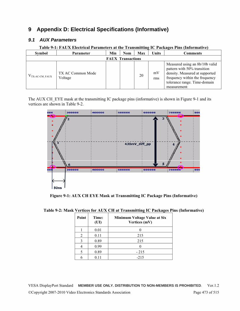
VESA DisplayPort Standard MEMBER USE ONLY. DISTRIBUTION TO NON-MEMBERS IS PROHIBITED. Ver.1.2
©Copyright 2007-2010 Video Electronics Standards Association Page 473 of 515
9 Appendix D: Electrical Specifications (Informative)
9.1 AUX Parameters Table 9-1: FAUX Electrical Parameters at the Transmitting IC Packages Pins (Informative)
Symbol Parameter Min Nom Max Units Comments FAUX Transactions
VTX-AC-CM_FAUX TX AC Common Mode Voltage 20
mV rms
Measured using an 8b/10b valid pattern with 50% transition density. Measured at supported frequency within the frequency tolerance range. Time-domain measurement
The AUX CH_EYE mask at the transmitting IC package pins (informative) is shown in Figure 9-1 and its vertices are shown in Table 9-2.
Figure 9-1: AUX CH EYE Mask at Transmitting IC Package Pins (Informative)
Table 9-2: Mask Vertices for AUX CH at Transmitting IC Packages Pins (Informative)
Point Time: (UI)
Minimum Voltage Value at Six Vertices (mV)
1 0.01 0 2 0.11 215 3 0.89 215 4 0.99 0 5 0.89 - 215 6 0.11 -215
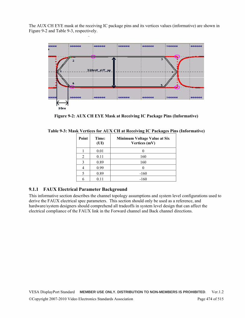
VESA DisplayPort Standard MEMBER USE ONLY. DISTRIBUTION TO NON-MEMBERS IS PROHIBITED. Ver.1.2
©Copyright 2007-2010 Video Electronics Standards Association Page 474 of 515
The AUX CH EYE mask at the receiving IC package pins and its vertices values (informative) are shown in Figure 9-2 and Table 9-3, respectively.
Figure 9-2: AUX CH EYE Mask at Receiving IC Package Pins (Informative)
Table 9-3: Mask Vertices for AUX CH at Receiving IC Packages Pins (Informative)
Point Time: (UI)
Minimum Voltage Value at Six Vertices (mV)
1 0.01 0 2 0.11 160 3 0.89 160 4 0.99 0 5 0.89 -160 6 0.11 -160
9.1.1 FAUX Electrical Parameter Background This informative section describes the channel topology assumptions and system level configurations used to derive the FAUX electrical spec parameters. This section should only be used as a reference, and hardware/system designers should comprehend all tradeoffs in system level design that can affect the electrical compliance of the FAUX link in the Forward channel and Back channel directions.
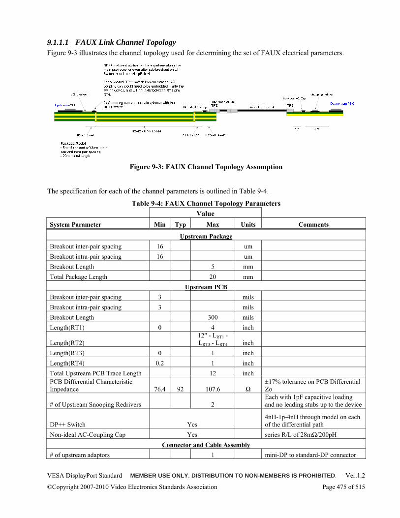
VESA DisplayPort Standard MEMBER USE ONLY. DISTRIBUTION TO NON-MEMBERS IS PROHIBITED. Ver.1.2
©Copyright 2007-2010 Video Electronics Standards Association Page 475 of 515
9.1.1.1 FAUX Link Channel Topology Figure 9-3 illustrates the channel topology used for determining the set of FAUX electrical parameters.
Figure 9-3: FAUX Channel Topology Assumption
The specification for each of the channel parameters is outlined in Table 9-4.
Table 9-4: FAUX Channel Topology Parameters Value System Parameter Min Typ Max Units Comments
Upstream Package Breakout inter-pair spacing 16 um Breakout intra-pair spacing 16 um Breakout Length 5 mm Total Package Length 20 mm
Upstream PCB Breakout inter-pair spacing 3 mils Breakout intra-pair spacing 3 mils Breakout Length 300 mils Length(RT1) 0 4 inch
Length(RT2) 12" - LRT1 - LRT3 - LRT4 inch
Length(RT3) 0 1 inch Length(RT4) 0.2 1 inch Total Upstream PCB Trace Length 12 inch PCB Differential Characteristic Impedance 76.4 92 107.6 Ω
±17% tolerance on PCB Differential Zo
# of Upstream Snooping Redrivers 2 Each with 1pF capacitive loading and no leading stubs up to the device
DP++ Switch Yes 4nH-1p-4nH through model on each of the differential path
Non-ideal AC-Coupling Cap Yes series R/L of 28mΩ/200pH Connector and Cable Assembly
# of upstream adaptors 1 mini-DP to standard-DP connector
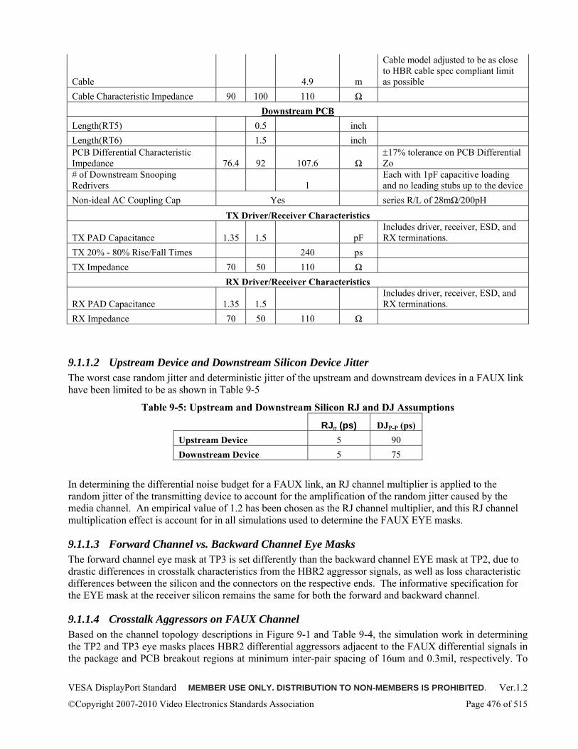
VESA DisplayPort Standard MEMBER USE ONLY. DISTRIBUTION TO NON-MEMBERS IS PROHIBITED. Ver.1.2
©Copyright 2007-2010 Video Electronics Standards Association Page 476 of 515
Cable 4.9 m
Cable model adjusted to be as close to HBR cable spec compliant limit as possible
Cable Characteristic Impedance 90 100 110 Ω Downstream PCB
Length(RT5) 0.5 inch Length(RT6) 1.5 inch PCB Differential Characteristic Impedance 76.4 92 107.6 Ω
±17% tolerance on PCB Differential Zo
# of Downstream Snooping Redrivers 1
Each with 1pF capacitive loading and no leading stubs up to the device
Non-ideal AC Coupling Cap Yes series R/L of 28mΩ/200pH TX Driver/Receiver Characteristics
TX PAD Capacitance 1.35 1.5 pF Includes driver, receiver, ESD, and RX terminations.
TX 20% - 80% Rise/Fall Times 240 ps TX Impedance 70 50 110 Ω
RX Driver/Receiver Characteristics
RX PAD Capacitance 1.35 1.5 Includes driver, receiver, ESD, and RX terminations.
RX Impedance 70 50 110 Ω
9.1.1.2 Upstream Device and Downstream Silicon Device Jitter The worst case random jitter and deterministic jitter of the upstream and downstream devices in a FAUX link have been limited to be as shown in Table 9-5
Table 9-5: Upstream and Downstream Silicon RJ and DJ Assumptions
RJσ (ps) DJP-P (ps) Upstream Device 5 90 Downstream Device 5 75
In determining the differential noise budget for a FAUX link, an RJ channel multiplier is applied to the random jitter of the transmitting device to account for the amplification of the random jitter caused by the media channel. An empirical value of 1.2 has been chosen as the RJ channel multiplier, and this RJ channel multiplication effect is account for in all simulations used to determine the FAUX EYE masks.
9.1.1.3 Forward Channel vs. Backward Channel Eye Masks The forward channel eye mask at TP3 is set differently than the backward channel EYE mask at TP2, due to drastic differences in crosstalk characteristics from the HBR2 aggressor signals, as well as loss characteristic differences between the silicon and the connectors on the respective ends. The informative specification for the EYE mask at the receiver silicon remains the same for both the forward and backward channel.
9.1.1.4 Crosstalk Aggressors on FAUX Channel Based on the channel topology descriptions in Figure 9-1 and Table 9-4, the simulation work in determining the TP2 and TP3 eye masks places HBR2 differential aggressors adjacent to the FAUX differential signals in the package and PCB breakout regions at minimum inter-pair spacing of 16um and 0.3mil, respectively. To
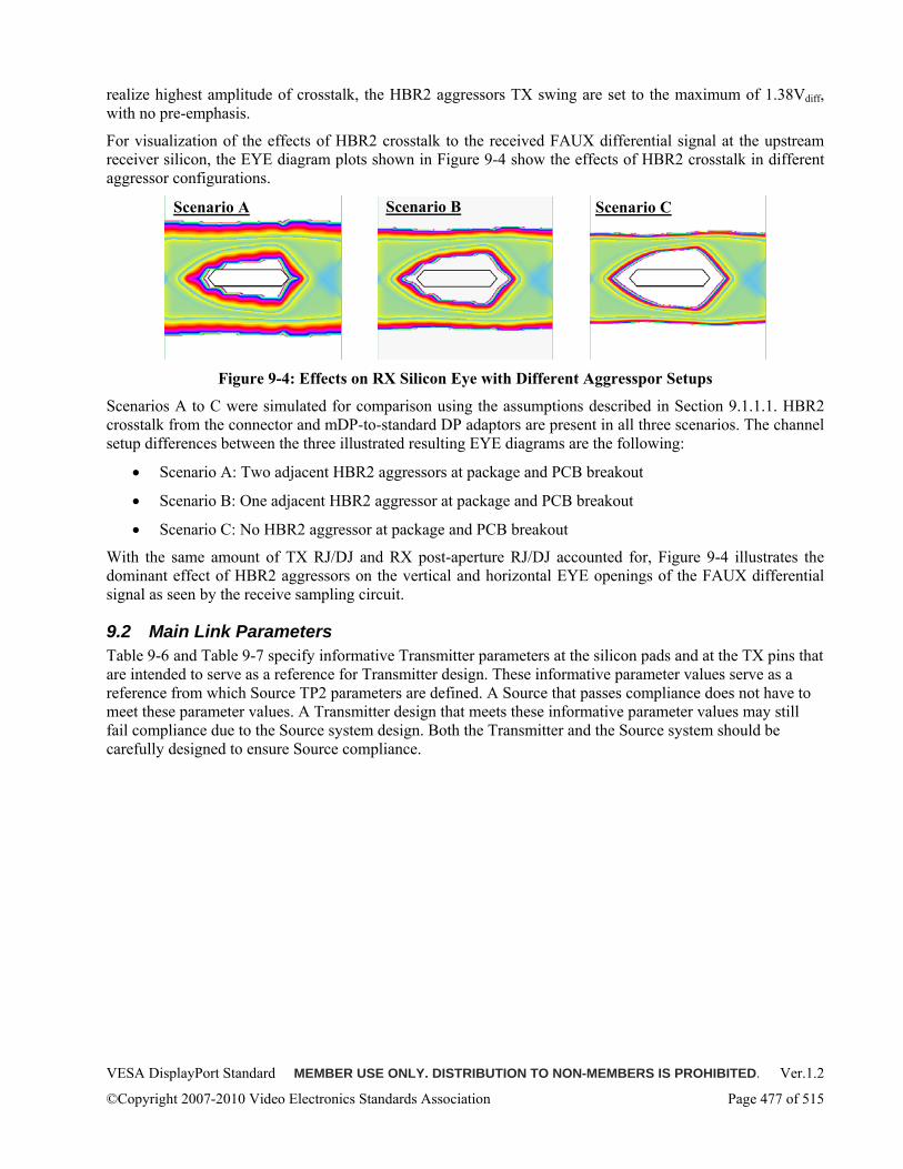
VESA DisplayPort Standard MEMBER USE ONLY. DISTRIBUTION TO NON-MEMBERS IS PROHIBITED. Ver.1.2
©Copyright 2007-2010 Video Electronics Standards Association Page 477 of 515
realize highest amplitude of crosstalk, the HBR2 aggressors TX swing are set to the maximum of 1.38Vdiff, with no pre-emphasis.
For visualization of the effects of HBR2 crosstalk to the received FAUX differential signal at the upstream receiver silicon, the EYE diagram plots shown in Figure 9-4 show the effects of HBR2 crosstalk in different aggressor configurations.
Figure 9-4: Effects on RX Silicon Eye with Different Aggresspor Setups
Scenarios A to C were simulated for comparison using the assumptions described in Section 9.1.1.1. HBR2 crosstalk from the connector and mDP-to-standard DP adaptors are present in all three scenarios. The channel setup differences between the three illustrated resulting EYE diagrams are the following:
• Scenario A: Two adjacent HBR2 aggressors at package and PCB breakout
• Scenario B: One adjacent HBR2 aggressor at package and PCB breakout
• Scenario C: No HBR2 aggressor at package and PCB breakout
With the same amount of TX RJ/DJ and RX post-aperture RJ/DJ accounted for, Figure 9-4 illustrates the dominant effect of HBR2 aggressors on the vertical and horizontal EYE openings of the FAUX differential signal as seen by the receive sampling circuit.
9.2 Main Link Parameters Table 9-6 and Table 9-7 specify informative Transmitter parameters at the silicon pads and at the TX pins that are intended to serve as a reference for Transmitter design. These informative parameter values serve as a reference from which Source TP2 parameters are defined. A Source that passes compliance does not have to meet these parameter values. A Transmitter design that meets these informative parameter values may still fail compliance due to the Source system design. Both the Transmitter and the Source system should be carefully designed to ensure Source compliance.
Scenario A Scenario B Scenario C
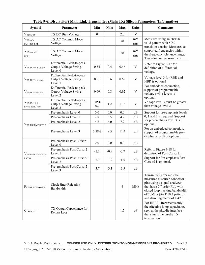
VESA DisplayPort Standard MEMBER USE ONLY. DISTRIBUTION TO NON-MEMBERS IS PROHIBITED. Ver.1.2
©Copyright 2007-2010 Video Electronics Standards Association Page 478 of 515
Table 9-6: DisplayPort Main Link Transmitter (Main TX) Silicon Parameters (Informative)
Symbol Parameter Min Nom Max Units Comments
VBIAS_TX TX DC Bias Voltage 0 2.0 V VTX-AC-
CM_HBR_RBR TX AC Common Mode Voltage 20
mV rms
VTX-AC-CM
HBR2 TX AC Common Mode Voltage 30
mV rms
Measured using an 8b/10b valid pattern with 50% transition density. Measured at supported frequencies within the frequency tolerance range. Time-domain measurement
VTX-DIFFp-p-Level0 Differential Peak-to-peak Output Voltage Swing Level 0
0.34 0.4 0.46 V
VTX-DIFFp-p-Level1 Differential Peak-to-peak Output Voltage Swing Level 1
0.51 0.6 0.68 V
VTX-DIFFp-p-Level2 Differential Peak-to-peak Output Voltage Swing Level 2
0.69 0.8 0.92 V
VTX-DIFFp-p-
Level3_RBR_HBR
Differential Peak-to-peak Output Voltage Swing Level 3
0.851.02 1.2 1.38 V
Refer to Figure 3-17 for definition of differential voltage. Voltage level 3 for RBR and HBR is optional For embedded connection, support of programmable voltage swing levels is optional. Voltage level 3 must be greater than voltage level 2
Pre-emphasis Level 0 0.0 0.0 0.0 dB Pre-emphasis Level 1 2.8 3.5 4.2 dB Pre-emphasis Level 2 4.8 6.0 7.2 dB
VTX-PREEMP-RATIO
Pre-emphasis Level 3 7.57.6 9.5 11.4 dB
Support for pre-emphasis levels 0, 1 and 2 is required. Support for pre-emphasis level 3 is optional. For an embedded connection, support of programmable pre-emphasis levels is optional.
Pre-emphasis Post Cursor2 Level 0 0.0 0.0 0.0 dB
Pre-emphasis Post Cursor2 Level 1 -1.1 -0.9 -0.7 dB
Pre-emphasis Post Cursor2 Level 2 -2.3 -1.9 -1.5 dB
VTX-PREEMP-POST2-
RATIO
Pre-emphasis Post Cursor2 Level 3 -3.7 -3.1 -2.5 dB
Refer to Figure 3-18 for definition of Post Cursor2. Support for Pre-emphasis Post Cursor2 is optional.
FTX-REJECTION-BW Clock Jitter Rejection Bandwidth 4 MHz
Transmitter jitter must be measured at source connector pins using a signal analyzer that has a 2nd order PLL with closed loop tracking bandwidth of 20MHz (for D10.2 pattern) and damping factor of 1.428
CTX-OUTPUT TX Output Capacitance for Return Loss 1.5 pF
For HBR2. Represents only the effective lump capacitance seen at the pkg/die interface that shunts the on-die TX termination.
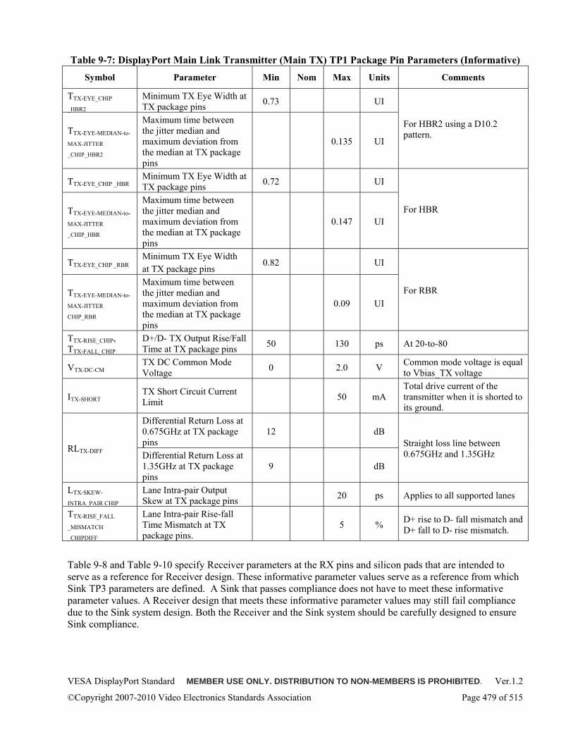
VESA DisplayPort Standard MEMBER USE ONLY. DISTRIBUTION TO NON-MEMBERS IS PROHIBITED. Ver.1.2
©Copyright 2007-2010 Video Electronics Standards Association Page 479 of 515
Table 9-7: DisplayPort Main Link Transmitter (Main TX) TP1 Package Pin Parameters (Informative)
Symbol Parameter Min Nom Max Units Comments
TTX-EYE_CHIP
_HBR2 Minimum TX Eye Width at TX package pins 0.73 UI
TTX-EYE-MEDIAN-to-
MAX-JITTER
_CHIP_HBR2
Maximum time between the jitter median and maximum deviation from the median at TX package pins
0.135 UI
For HBR2 using a D10.2 pattern.
TTX-EYE_CHIP _HBR Minimum TX Eye Width at TX package pins 0.72 UI
TTX-EYE-MEDIAN-to-
MAX-JITTER
_CHIP_HBR
Maximum time between the jitter median and maximum deviation from the median at TX package pins
0.147 UI For HBR
TTX-EYE_CHIP _RBR Minimum TX Eye Width at TX package pins
0.82 UI
TTX-EYE-MEDIAN-to-
MAX-JITTER
CHIP_RBR
Maximum time between the jitter median and maximum deviation from the median at TX package pins
0.09 UI For RBR
TTX-RISE_CHIP, TTX-FALL_CHIP
D+/D- TX Output Rise/Fall Time at TX package pins 50 130 ps At 20-to-80
VTX-DC-CM TX DC Common Mode Voltage 0 2.0 V Common mode voltage is equal
to Vbias_TX voltage
ITX-SHORT TX Short Circuit Current Limit 50 mA
Total drive current of the transmitter when it is shorted to its ground.
Differential Return Loss at 0.675GHz at TX package pins
12 dB
RLTX-DIFF Differential Return Loss at 1.35GHz at TX package pins
9 dB
Straight loss line between 0.675GHz and 1.35GHz
LTX-SKEW-
INTRA_PAIR CHIP Lane Intra-pair Output Skew at TX package pins 20 ps Applies to all supported lanes
TTX-RISE_FALL
_MISMATCH
_CHIPDIFF
Lane Intra-pair Rise-fall Time Mismatch at TX package pins.
5 % D+ rise to D- fall mismatch and D+ fall to D- rise mismatch.
Table 9-8 and Table 9-10 specify Receiver parameters at the RX pins and silicon pads that are intended to serve as a reference for Receiver design. These informative parameter values serve as a reference from which Sink TP3 parameters are defined. A Sink that passes compliance does not have to meet these informative parameter values. A Receiver design that meets these informative parameter values may still fail compliance due to the Sink system design. Both the Receiver and the Sink system should be carefully designed to ensure Sink compliance.
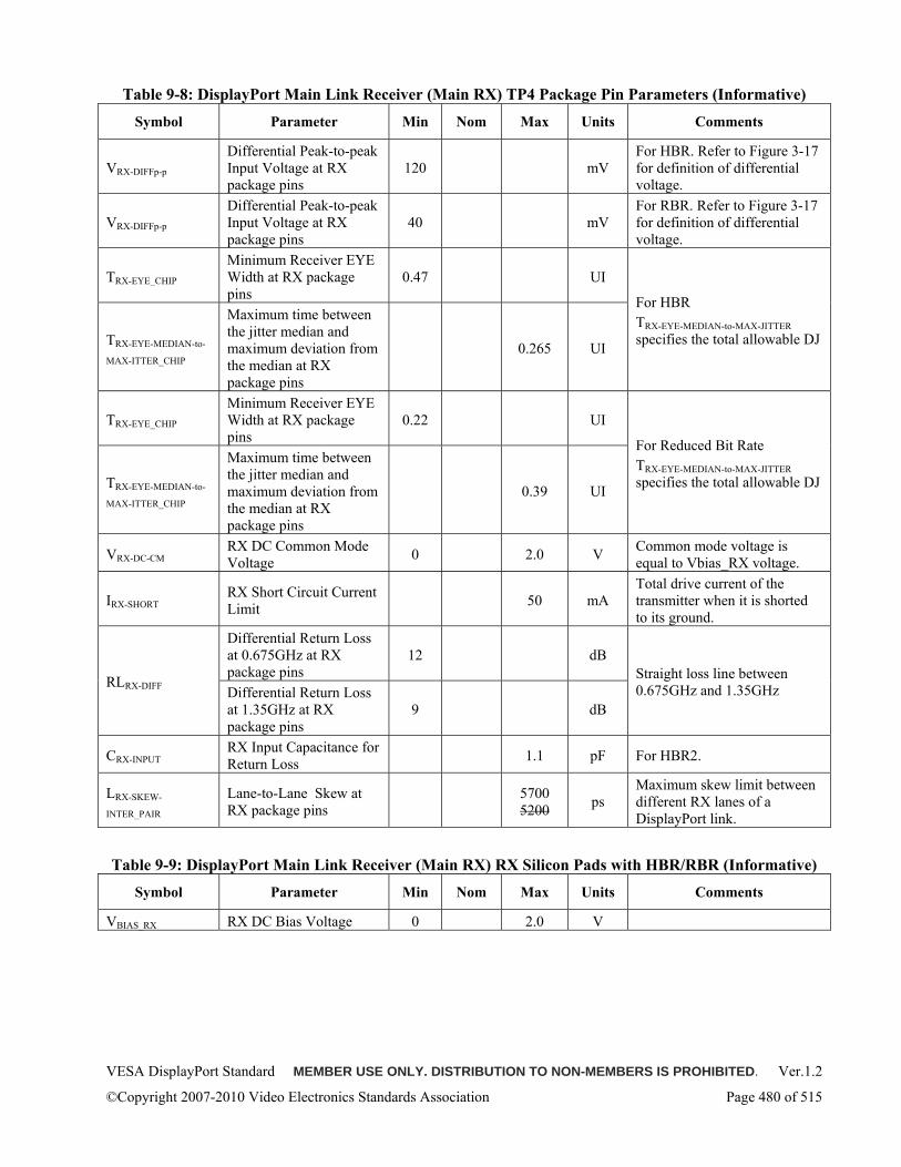
VESA DisplayPort Standard MEMBER USE ONLY. DISTRIBUTION TO NON-MEMBERS IS PROHIBITED. Ver.1.2
©Copyright 2007-2010 Video Electronics Standards Association Page 480 of 515
Table 9-8: DisplayPort Main Link Receiver (Main RX) TP4 Package Pin Parameters (Informative)
Symbol Parameter Min Nom Max Units Comments
VRX-DIFFp-p Differential Peak-to-peak Input Voltage at RX package pins
120 mV For HBR. Refer to Figure 3-17 for definition of differential voltage.
VRX-DIFFp-p Differential Peak-to-peak Input Voltage at RX package pins
40 mV For RBR. Refer to Figure 3-17 for definition of differential voltage.
TRX-EYE_CHIP Minimum Receiver EYE Width at RX package pins
0.47 UI
TRX-EYE-MEDIAN-to-
MAX-ITTER_CHIP
Maximum time between the jitter median and maximum deviation from the median at RX package pins
0.265 UI
For HBR TRX-EYE-MEDIAN-to-MAX-JITTER specifies the total allowable DJ
TRX-EYE_CHIP Minimum Receiver EYE Width at RX package pins
0.22 UI
TRX-EYE-MEDIAN-to-
MAX-ITTER_CHIP
Maximum time between the jitter median and maximum deviation from the median at RX package pins
0.39 UI
For Reduced Bit Rate TRX-EYE-MEDIAN-to-MAX-JITTER specifies the total allowable DJ
VRX-DC-CM RX DC Common Mode Voltage 0 2.0 V Common mode voltage is
equal to Vbias_RX voltage.
IRX-SHORT RX Short Circuit Current Limit 50 mA
Total drive current of the transmitter when it is shorted to its ground.
Differential Return Loss at 0.675GHz at RX package pins
12 dB
RLRX-DIFF Differential Return Loss at 1.35GHz at RX package pins
9 dB
Straight loss line between 0.675GHz and 1.35GHz
CRX-INPUT RX Input Capacitance for Return Loss 1.1 pF For HBR2.
LRX-SKEW-
INTER_PAIR Lane-to-Lane Skew at RX package pins 5700
5200 ps Maximum skew limit between different RX lanes of a DisplayPort link.
Table 9-9: DisplayPort Main Link Receiver (Main RX) RX Silicon Pads with HBR/RBR (Informative)
Symbol Parameter Min Nom Max Units Comments
VBIAS_RX RX DC Bias Voltage 0 2.0 V
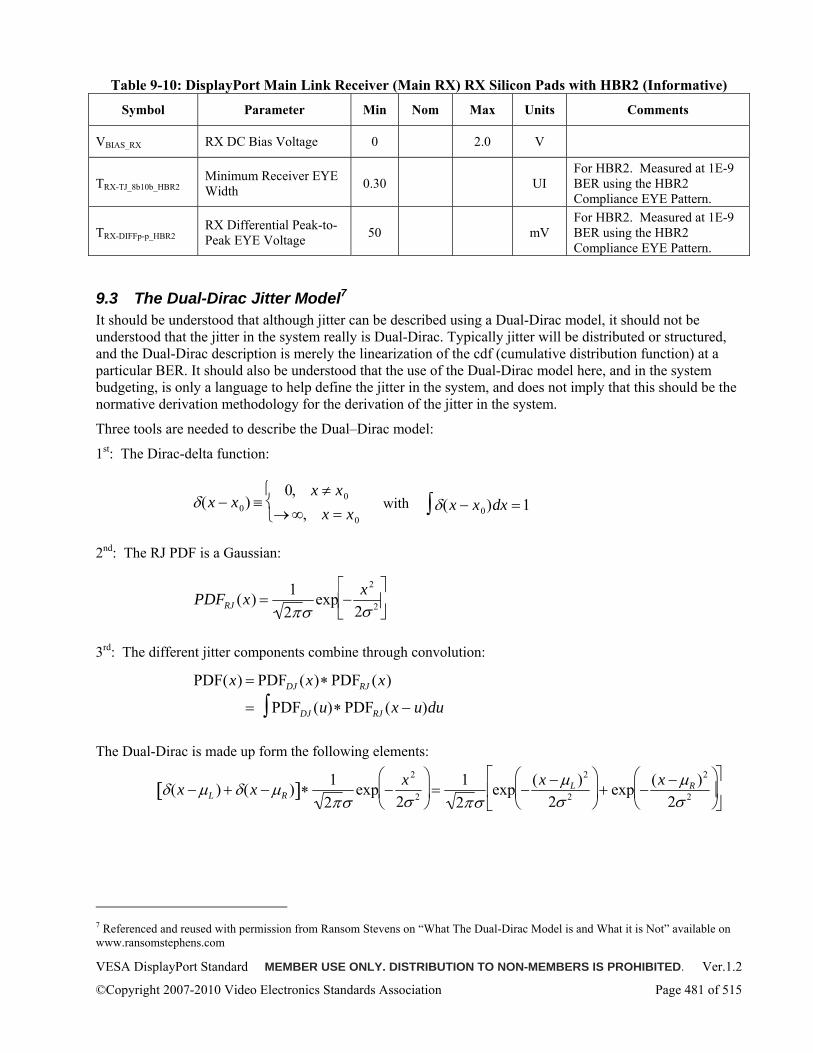
VESA DisplayPort Standard MEMBER USE ONLY. DISTRIBUTION TO NON-MEMBERS IS PROHIBITED. Ver.1.2
©Copyright 2007-2010 Video Electronics Standards Association Page 481 of 515
Table 9-10: DisplayPort Main Link Receiver (Main RX) RX Silicon Pads with HBR2 (Informative)
Symbol Parameter Min Nom Max Units Comments
VBIAS_RX RX DC Bias Voltage 0 2.0 V
TRX-TJ_8b10b_HBR2 Minimum Receiver EYE Width 0.30 UI
For HBR2. Measured at 1E-9 BER using the HBR2 Compliance EYE Pattern.
TRX-DIFFp-p_HBR2 RX Differential Peak-to-Peak EYE Voltage 50 mV
For HBR2. Measured at 1E-9 BER using the HBR2 Compliance EYE Pattern.
9.3 The Dual-Dirac Jitter Model7 It should be understood that although jitter can be described using a Dual-Dirac model, it should not be understood that the jitter in the system really is Dual-Dirac. Typically jitter will be distributed or structured, and the Dual-Dirac description is merely the linearization of the cdf (cumulative distribution function) at a particular BER. It should also be understood that the use of the Dual-Dirac model here, and in the system budgeting, is only a language to help define the jitter in the system, and does not imply that this should be the normative derivation methodology for the derivation of the jitter in the system.
Three tools are needed to describe the Dual–Dirac model:
1st: The Dirac-delta function:
with
2nd: The RJ PDF is a Gaussian:
3rd: The different jitter components combine through convolution:
The Dual-Dirac is made up form the following elements:
7 Referenced and reused with permission from Ransom Stevens on “What The Dual-Dirac Model is and What it is Not” available on www.ransomstephens.com
δ(x − x0) ≡0, x ≠ x0
→ ∞, x = x0
⎧ ⎨ ⎩
δ(x − x0)dx∫ =1
PDFRJ (x) =1
2πσexp −
x 2
2σ 2
⎡
⎣ ⎢
⎤
⎦ ⎥
PDF(x) = PDFDJ (x) ∗ PDFRJ (x)
= PDFDJ (u) ∗PDFRJ (x − u)du∫
δ(x − μL ) + δ(x − μR )[ ]∗1
2πσexp −
x 2
2σ 2
⎛
⎝ ⎜
⎞
⎠ ⎟ =
12πσ
exp −(x − μL )2
2σ 2
⎛
⎝ ⎜
⎞
⎠ ⎟ + exp −
(x − μR )2
2σ 2
⎛
⎝ ⎜
⎞
⎠ ⎟
⎡
⎣ ⎢
⎤
⎦ ⎥
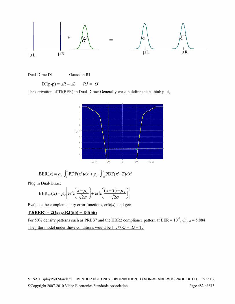
VESA DisplayPort Standard MEMBER USE ONLY. DISTRIBUTION TO NON-MEMBERS IS PROHIBITED. Ver.1.2
©Copyright 2007-2010 Video Electronics Standards Association Page 482 of 515
Dual-Dirac DJ Gaussian RJ
DJ(p-p) = μR – μL RJ = σ
The derivation of TJ(BER) in Dual-Dirac: Generally we can define the bathtub plot,
Plug in Dual-Dirac:
Evaluate the complementary error functions, erfc(x), and get:
TJ(BER) = 2QBER×RJ(δδ) + DJ(δδ) For 50% density patterns such as PRBS7 and the HBR2 compliance pattern at BER = 10-9, QBER = 5.884
The jitter model under these conditions would be 11.77RJ + DJ = TJ
∗ =σ
μL μR μL
μR
σ σ σ
BER(x) = ρT PDF(x')dx'x
∞∫ + ρT PDF(x '−T)dx '−∞
x∫
BERδδ (x) = ρT erfc x − μL
2σ⎛ ⎝ ⎜
⎞ ⎠ ⎟ + erfc (x − T) − μR
2σ⎛ ⎝ ⎜
⎞ ⎠ ⎟
⎡
⎣ ⎢
⎤
⎦ ⎥
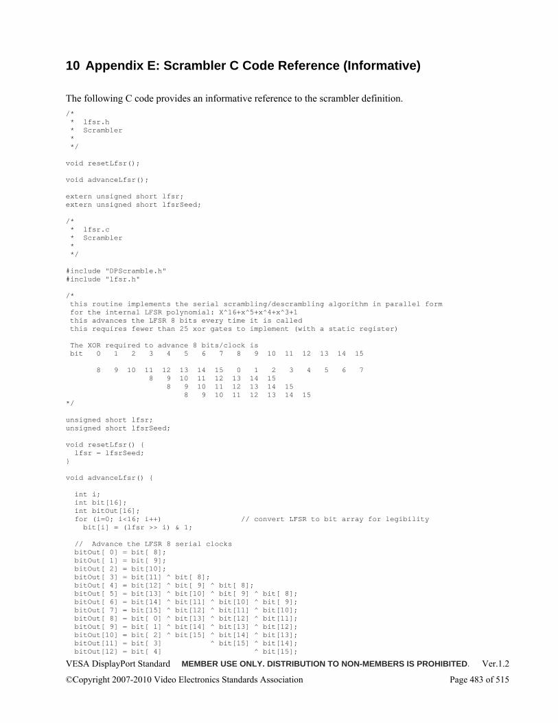
VESA DisplayPort Standard MEMBER USE ONLY. DISTRIBUTION TO NON-MEMBERS IS PROHIBITED. Ver.1.2
©Copyright 2007-2010 Video Electronics Standards Association Page 483 of 515
10 Appendix E: Scrambler C Code Reference (Informative)
The following C code provides an informative reference to the scrambler definition. /* * lfsr.h * Scrambler * */ void resetLfsr(); void advanceLfsr(); extern unsigned short lfsr; extern unsigned short lfsrSeed; /* * lfsr.c * Scrambler * */ #include "DPScramble.h" #include "lfsr.h" /* this routine implements the serial scrambling/descrambling algorithm in parallel form for the internal LFSR polynomial: X^16+x^5+x^4+x^3+1 this advances the LFSR 8 bits every time it is called this requires fewer than 25 xor gates to implement (with a static register) The XOR required to advance 8 bits/clock is bit 0 1 2 3 4 5 6 7 8 9 10 11 12 13 14 15 8 9 10 11 12 13 14 15 0 1 2 3 4 5 6 7 8 9 10 11 12 13 14 15 8 9 10 11 12 13 14 15 8 9 10 11 12 13 14 15 */ unsigned short lfsr; unsigned short lfsrSeed; void resetLfsr() lfsr = lfsrSeed; void advanceLfsr() int i; int bit[16]; int bitOut[16]; for (i=0; i<16; i++) // convert LFSR to bit array for legibility bit[i] = (lfsr >> i) & 1; // Advance the LFSR 8 serial clocks bitOut[ 0] = bit[ 8]; bitOut[ 1] = bit[ 9]; bitOut[ 2] = bit[10]; bitOut[ 3] = bit[11] ^ bit[ 8]; bitOut[ 4] = bit[12] ^ bit[ 9] ^ bit[ 8]; bitOut[ 5] = bit[13] ^ bit[10] ^ bit[ 9] ^ bit[ 8]; bitOut[ 6] = bit[14] ^ bit[11] ^ bit[10] ^ bit[ 9]; bitOut[ 7] = bit[15] ^ bit[12] ^ bit[11] ^ bit[10]; bitOut[ 8] = bit[ 0] ^ bit[13] ^ bit[12] ^ bit[11]; bitOut[ 9] = bit[ 1] ^ bit[14] ^ bit[13] ^ bit[12]; bitOut[10] = bit[ 2] ^ bit[15] ^ bit[14] ^ bit[13]; bitOut[11] = bit[ 3] ^ bit[15] ^ bit[14]; bitOut[12] = bit[ 4] ^ bit[15];
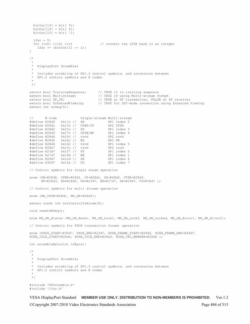
VESA DisplayPort Standard MEMBER USE ONLY. DISTRIBUTION TO NON-MEMBERS IS PROHIBITED. Ver.1.2
©Copyright 2007-2010 Video Electronics Standards Association Page 484 of 515
bitOut[13] = bit[ 5]; bitOut[14] = bit[ 6]; bitOut[15] = bit[ 7]; lfsr = 0; for (i=0; i<16; i++) // convert the LFSR back to an integer lfsr += (bitOut[i] << i); /* * * DisplayPort Scrambler * * Includes scrabling of DP1.2 control symbols, and conversion between * DP1.2 control symbols and K codes * */ extern bool TrainingSequence; // TRUE if in training sequence extern bool Multistream; // TRUE if using Multi-stream format extern bool DP_TX; // TRUE at DP transmitter, FALSE at DP receiver extern bool EnhancedFraming; // TRUE for SST-mode connection using Enhanced Framing extern int srSeq[4]; // K-code Single-stream Multi-stream #define K28d0 0x11c // SR GP1 index 2 #define K28d1 0x13c // CPBS/CP GP2 CPSR #define K28d2 0x15c // SS GP1 index 3 #define K28d3 0x17c // CPSR/BF GP1 index 4 #define K28d4 0x19c // rsvd GP2 rsvd #define K28d5 0x1bc // BS GP2 SR #define K28d6 0x1dc // rsvd GP1 index 5 #define K28d7 0x1fc // rsvd GP2 rsvd #define K23d7 0x1f7 // FE GP1 index 0 #define K27d7 0x1fb // BE GP1 index 1 #define K29d7 0x1fd // SE GP1 index 6 #define K30d7 0x1fe // FS GP1 index 7 // Control symbols for single steam operation enum SR=K28d0, CPBS=K28d1, CP=K28d1, SS=K28d2, CPSR=K28d3, BF=K28d3, BS=K28d5, FE=K23d7, BE=K27d7, SE=K29d7, FS=K30d7 ; // Control symbols for multi stream operation enum MS_CPSR=K28d1, MS_SR=K28d5; extern const int scrControlToKcode[8]; void resetSRSeq(); enum MS_SR_States MS_SR_Reset, MS_SR_Lock1, MS_SR_Lock2, MS_SR_Locked, MS_SR_Error1, MS_SR_Error2; // Control symbols for FAUX transaction format operation enum FAUX_START=K30d7, FAUX_END=K23d7, XUSB_FRAME_START=K28d2, XUSB_FRAME_END=K28d7, XUSB_IDLE_START=K28d0, XUSB_IDLE_END=K28d3, XUSB_CRC_MARKER=K28d6 ; int scrambleByte(int inByte); /* * * DisplayPOrt Scrambler * * Includes scrabling of DP1.2 control symbols, and conversion between * DP1.2 control symbols and K codes * */ #include "DPScramble.h" #include "lfsr.h"
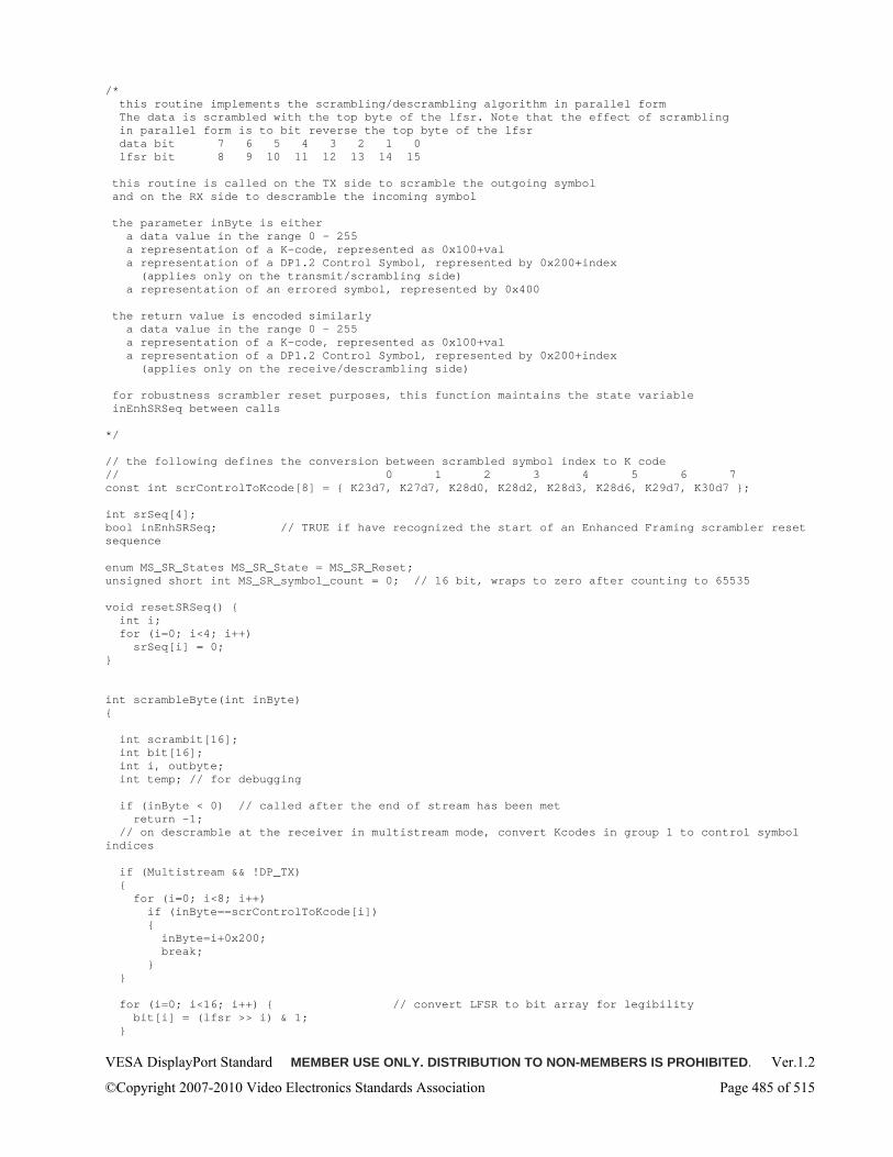
VESA DisplayPort Standard MEMBER USE ONLY. DISTRIBUTION TO NON-MEMBERS IS PROHIBITED. Ver.1.2
©Copyright 2007-2010 Video Electronics Standards Association Page 485 of 515
/* this routine implements the scrambling/descrambling algorithm in parallel form The data is scrambled with the top byte of the lfsr. Note that the effect of scrambling in parallel form is to bit reverse the top byte of the lfsr data bit 7 6 5 4 3 2 1 0 lfsr bit 8 9 10 11 12 13 14 15 this routine is called on the TX side to scramble the outgoing symbol and on the RX side to descramble the incoming symbol the parameter inByte is either a data value in the range 0 - 255 a representation of a K-code, represented as 0x100+val a representation of a DP1.2 Control Symbol, represented by 0x200+index (applies only on the transmit/scrambling side) a representation of an errored symbol, represented by 0x400 the return value is encoded similarly a data value in the range 0 - 255 a representation of a K-code, represented as 0x100+val a representation of a DP1.2 Control Symbol, represented by 0x200+index (applies only on the receive/descrambling side) for robustness scrambler reset purposes, this function maintains the state variable inEnhSRSeq between calls */ // the following defines the conversion between scrambled symbol index to K code // 0 1 2 3 4 5 6 7 const int scrControlToKcode[8] = K23d7, K27d7, K28d0, K28d2, K28d3, K28d6, K29d7, K30d7 ; int srSeq[4]; bool inEnhSRSeq; // TRUE if have recognized the start of an Enhanced Framing scrambler reset sequence enum MS_SR_States MS_SR_State = MS_SR_Reset; unsigned short int MS_SR_symbol_count = 0; // 16 bit, wraps to zero after counting to 65535 void resetSRSeq() int i; for (i=0; i<4; i++) srSeq[i] = 0; int scrambleByte(int inByte) int scrambit[16]; int bit[16]; int i, outbyte; int temp; // for debugging if (inByte < 0) // called after the end of stream has been met return -1; // on descramble at the receiver in multistream mode, convert Kcodes in group 1 to control symbol indices if (Multistream && !DP_TX) for (i=0; i<8; i++) if (inByte==scrControlToKcode[i]) inByte=i+0x200; break; for (i=0; i<16; i++) // convert LFSR to bit array for legibility bit[i] = (lfsr >> i) & 1;
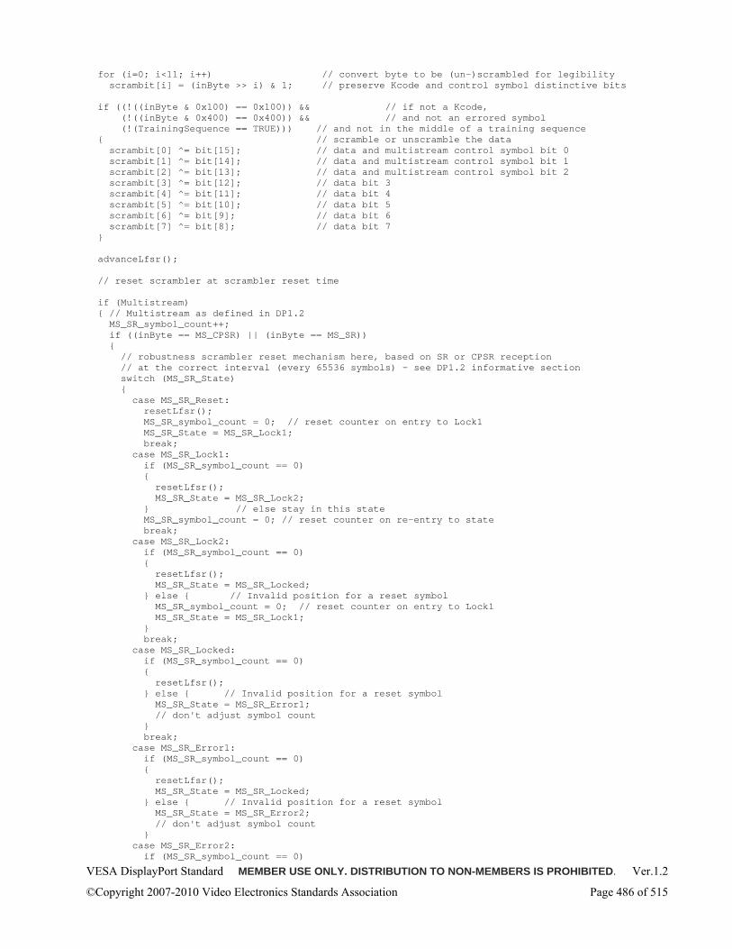
VESA DisplayPort Standard MEMBER USE ONLY. DISTRIBUTION TO NON-MEMBERS IS PROHIBITED. Ver.1.2
©Copyright 2007-2010 Video Electronics Standards Association Page 486 of 515
for (i=0; i<11; i++) // convert byte to be (un-)scrambled for legibility scrambit[i] = (inByte >> i) & 1; // preserve Kcode and control symbol distinctive bits if ((!((inByte & 0x100) == 0x100)) && // if not a Kcode, (!((inByte & 0x400) == 0x400)) && // and not an errored symbol (!(TrainingSequence == TRUE))) // and not in the middle of a training sequence // scramble or unscramble the data scrambit[0] ^= bit[15]; // data and multistream control symbol bit 0 scrambit[1] ^= bit[14]; // data and multistream control symbol bit 1 scrambit[2] ^= bit[13]; // data and multistream control symbol bit 2 scrambit[3] ^= bit[12]; // data bit 3 scrambit[4] ^= bit[11]; // data bit 4 scrambit[5] ^= bit[10]; // data bit 5 scrambit[6] ^= bit[9]; // data bit 6 scrambit[7] ^= bit[8]; // data bit 7 advanceLfsr(); // reset scrambler at scrambler reset time if (Multistream) // Multistream as defined in DP1.2 MS_SR_symbol_count++; if ((inByte == MS_CPSR) || (inByte == MS_SR)) // robustness scrambler reset mechanism here, based on SR or CPSR reception // at the correct interval (every 65536 symbols) - see DP1.2 informative section switch (MS_SR_State) case MS_SR_Reset: resetLfsr(); MS_SR_symbol_count = 0; // reset counter on entry to Lock1 MS_SR_State = MS_SR_Lock1; break; case MS_SR_Lock1: if (MS_SR_symbol_count == 0) resetLfsr(); MS_SR_State = MS_SR_Lock2; // else stay in this state MS_SR_symbol_count = 0; // reset counter on re-entry to state break; case MS_SR_Lock2: if (MS_SR_symbol_count == 0) resetLfsr(); MS_SR_State = MS_SR_Locked; else // Invalid position for a reset symbol MS_SR_symbol_count = 0; // reset counter on entry to Lock1 MS_SR_State = MS_SR_Lock1; break; case MS_SR_Locked: if (MS_SR_symbol_count == 0) resetLfsr(); else // Invalid position for a reset symbol MS_SR_State = MS_SR_Error1; // don't adjust symbol count break; case MS_SR_Error1: if (MS_SR_symbol_count == 0) resetLfsr(); MS_SR_State = MS_SR_Locked; else // Invalid position for a reset symbol MS_SR_State = MS_SR_Error2; // don't adjust symbol count case MS_SR_Error2: if (MS_SR_symbol_count == 0)
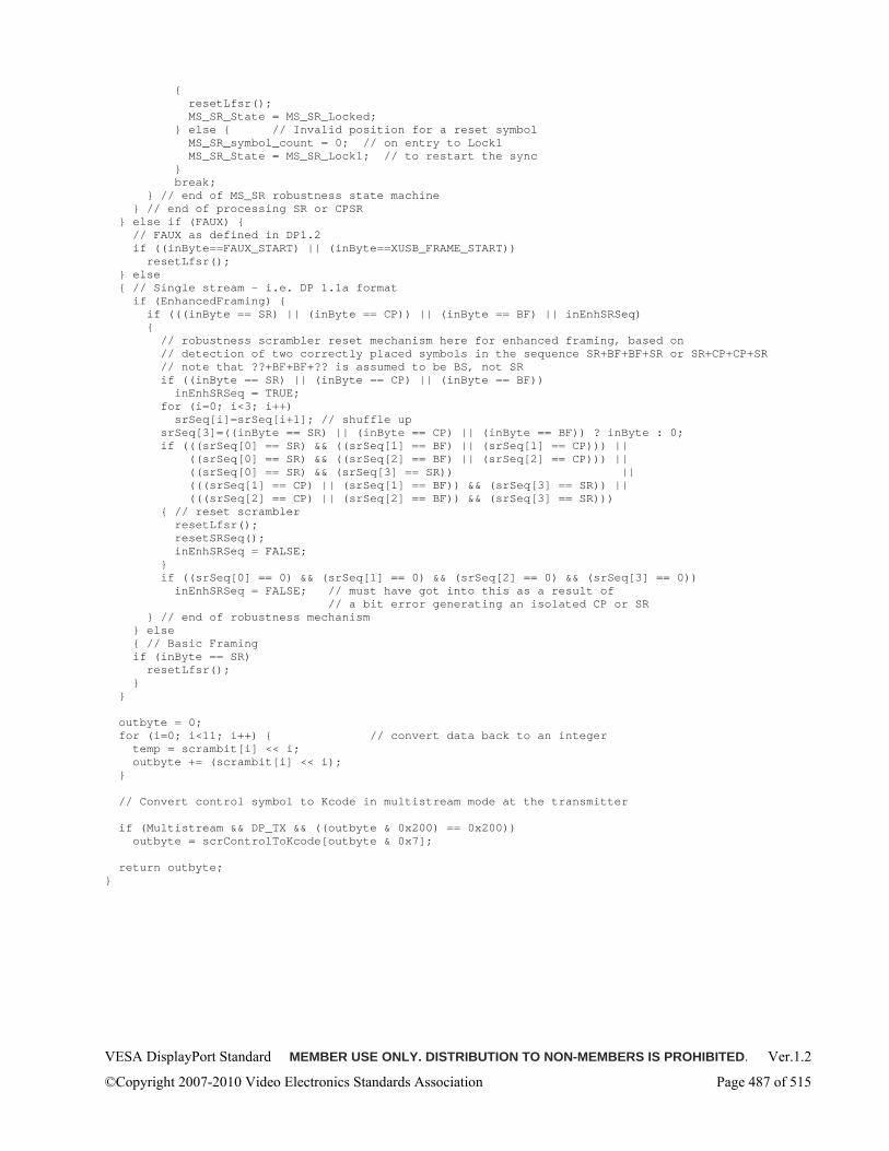
VESA DisplayPort Standard MEMBER USE ONLY. DISTRIBUTION TO NON-MEMBERS IS PROHIBITED. Ver.1.2
©Copyright 2007-2010 Video Electronics Standards Association Page 487 of 515
resetLfsr(); MS_SR_State = MS_SR_Locked; else // Invalid position for a reset symbol MS_SR_symbol_count = 0; // on entry to Lock1 MS_SR_State = MS_SR_Lock1; // to restart the sync break; // end of MS_SR robustness state machine // end of processing SR or CPSR else if (FAUX) // FAUX as defined in DP1.2 if ((inByte==FAUX_START) || (inByte==XUSB_FRAME_START)) resetLfsr(); else // Single stream - i.e. DP 1.1a format if (EnhancedFraming) if (((inByte == SR) || (inByte == CP)) || (inByte == BF) || inEnhSRSeq) // robustness scrambler reset mechanism here for enhanced framing, based on // detection of two correctly placed symbols in the sequence SR+BF+BF+SR or SR+CP+CP+SR // note that ??+BF+BF+?? is assumed to be BS, not SR if ((inByte == SR) || (inByte == CP) || (inByte == BF)) inEnhSRSeq = TRUE; for (i=0; i<3; i++) srSeq[i]=srSeq[i+1]; // shuffle up srSeq[3]=((inByte == SR) || (inByte == CP) || (inByte == BF)) ? inByte : 0; if (((srSeq[0] == SR) && ((srSeq[1] == BF) || (srSeq[1] == CP))) || ((srSeq[0] == SR) && ((srSeq[2] == BF) || (srSeq[2] == CP))) || ((srSeq[0] == SR) && (srSeq[3] == SR)) || (((srSeq[1] == CP) || (srSeq[1] == BF)) && (srSeq[3] == SR)) || (((srSeq[2] == CP) || (srSeq[2] == BF)) && (srSeq[3] == SR))) // reset scrambler resetLfsr(); resetSRSeq(); inEnhSRSeq = FALSE; if ((srSeq[0] == 0) && (srSeq[1] == 0) && (srSeq[2] == 0) && (srSeq[3] == 0)) inEnhSRSeq = FALSE; // must have got into this as a result of // a bit error generating an isolated CP or SR // end of robustness mechanism else // Basic Framing if (inByte == SR) resetLfsr(); outbyte = 0; for (i=0; i<11; i++) // convert data back to an integer temp = scrambit[i] << i; outbyte += (scrambit[i] << i); // Convert control symbol to Kcode in multistream mode at the transmitter if (Multistream && DP_TX && ((outbyte & 0x200) == 0x200)) outbyte = scrControlToKcode[outbyte & 0x7]; return outbyte;
VESA DisplayPort Standard MEMBER USE ONLY. DISTRIBUTION TO NON-MEMBERS IS PROHIBITED. Ver.1.2
©Copyright 2007-2010 Video Electronics Standards Association Page 488 of 515
11 Appendix F: Topology Management/Payload Bandwidth Management Usage Examples
This subject matter is to be covered in a separate addendum document for informative purposes.
VESA DisplayPort Standard MEMBER USE ONLY. DISTRIBUTION TO NON-MEMBERS IS PROHIBITED. Ver.1.2
©Copyright 2007-2010 Video Electronics Standards Association Page 489 of 515
12 Appendix G: Link Management During System Initialization (Informative)
12.1 Background Some DP Source solutions rely heavily on an operating system video/display driver to handle many of the higher-level functions in the DP protocol.
Immediately after boot (before the operating system is loaded) and in operating system safe mode, the product-specific video driver is not loaded. In these scenarios, the Video BIOS or equivalent is used to configure the graphics outputs. However, VBIOS does not typically implement interrupt handling, and as a result it cannot respond to link state changes that occur after the BIOS was initially invoked.
Implementing BIOS exception handling causes system incompatibility issues for discrete graphics cards, so this is not a feasible long-term solution.
12.2 Problem Statements
12.2.1 Problem #1: Sink Attached and Powered, but HPD Low Description: If a Sink device does not keep HPD asserted at all times when powered, then the Source may not detect the Sink when the VBIOS is invoked. In this case, the Source will not enable the output in question, even if that output is available.
Solution: The DP Sink device must keep HPD asserted unless it is in the OFF state. See Section 5.2.5.
12.2.2 Problem #2: Sink HPD Unplug Event Followed by Plug Event Description: If a Sink device is turned on, or is unplugged and re-plugged after a Source device is turned on and VBIOS invoked, the Source device that depends on VBIOS to do Link Training will not be able to train the link
Solution Case 1; In this case, the DP Source can detect HPD, but can run Fast Link Training only (training without using AUX transactions).
DP Source Device
• If video needs to be transmitted, run Fast Link Training to 1-lane RBR Link Configuration, and transmit 640x480 Safe Mode over the link
o 1-lane RBR/640x480 is supported by all DP Sink devices, and is the most likely to work without Full LT (Link Training)
o For this to work, the solution requires the DP Sink device to support Fast Link Training anticipating 1-lane RBR link configuration
DP Sink Device
• If capable of supporting Fast Link Training (optional RX feature in DP Standard)
o Be ready to receive Fast Link Training to 1-lane RBR link configuration and, upon CR_LOCK/SYMBOL_LOCK, a 640x480 video stream
This Standard:
• defines 1-lane RBR as the “default” link configuration for both the DP Source and DP Sink when no “last-known-good” link configuration exists, and
• has no impact on operation of or interoperation with a DP Source device fielding HPD and capable of running Full Link Training
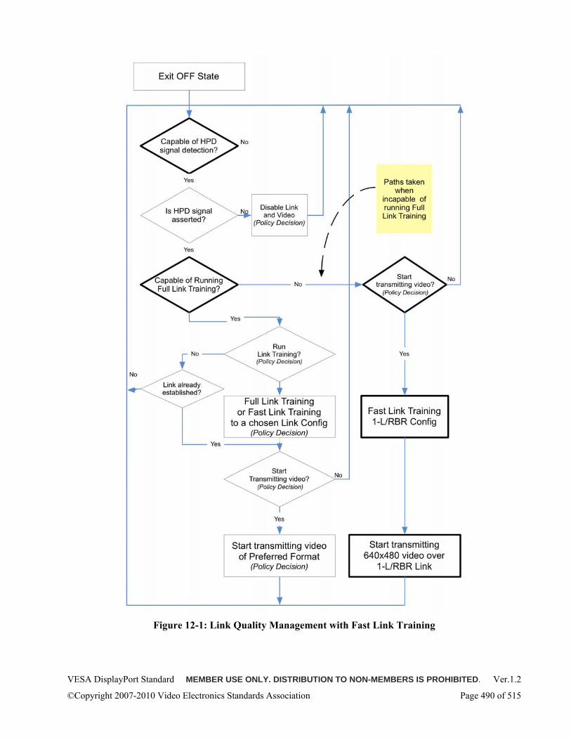
VESA DisplayPort Standard MEMBER USE ONLY. DISTRIBUTION TO NON-MEMBERS IS PROHIBITED. Ver.1.2
©Copyright 2007-2010 Video Electronics Standards Association Page 490 of 515
Figure 12-1: Link Quality Management with Fast Link Training
VESA DisplayPort Standard MEMBER USE ONLY. DISTRIBUTION TO NON-MEMBERS IS PROHIBITED. Ver.1.2
©Copyright 2007-2010 Video Electronics Standards Association Page 491 of 515
Solution Case 2; In this case, the DP Source cannot detect HPD
DP Source Device
• If no known-good link configuration (monitor connected or powered up after DP Source is powered up) AND need to transmit video, transmit 640x480 Safe Mode over 1-lane RBR Main Link
o 1-lane RBR/640x480 supported by all DP Sink devices, and the most likely to work without Full LT (Link Training)
o To avoid No Display requires DP Sink capable of receiving Main Link signal w/o LT anticipating 1-lane RBR link configuration
• If cable unplugged and plugged after the link was established, DP Source will continue transmitting video over previously established link configuration
o To avoid No Display requires DP Sink capable of receiving Main Link signal w/o LT anticipating the “last-known-good” link configuration; works if the same DP Sink is plugged back
DP Sink Device
• If capable of receiving Main Link signal w/o LT (RX feature not described in DP1.1a spec)
o Be ready to receive Main Link signal either to 1-lane RBR or the last-known-good link configuration
This proposal has no impact on operation of interoperation with a DP Source device fielding HPD and capable of running Full Link Training.
Figure 12-2 shows the Source side behavior and Figure 12-3 shows the Sink side Power State machine. In this case, the Sink Power State diagram is extended by the addition of State 2s for avoiding No Display when the DP Source is not capable of fielding HPD.
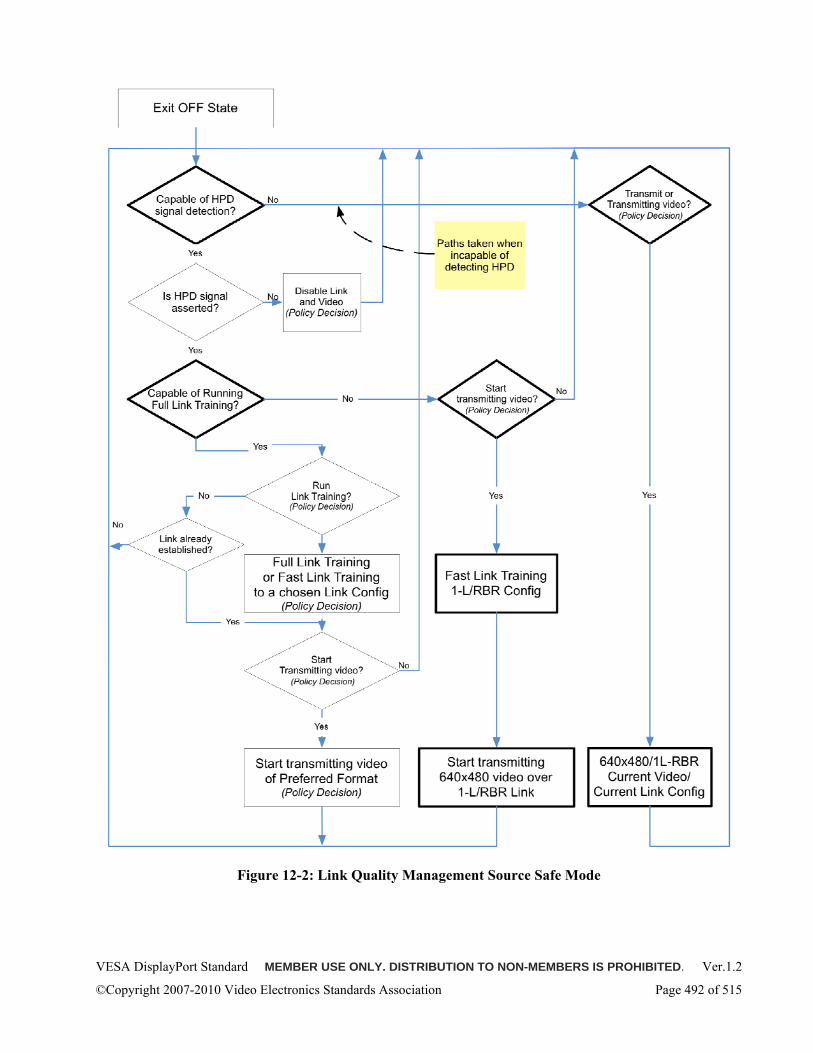
VESA DisplayPort Standard MEMBER USE ONLY. DISTRIBUTION TO NON-MEMBERS IS PROHIBITED. Ver.1.2
©Copyright 2007-2010 Video Electronics Standards Association Page 492 of 515
Figure 12-2: Link Quality Management Source Safe Mode
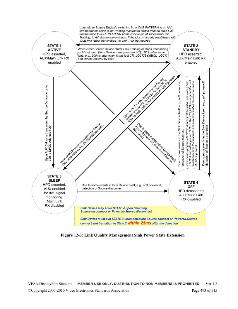
VESA DisplayPort Standard MEMBER USE ONLY. DISTRIBUTION TO NON-MEMBERS IS PROHIBITED. Ver.1.2
©Copyright 2007-2010 Video Electronics Standards Association Page 493 of 515
Figure 12-3: Link Quality Management Sink Power State Extension
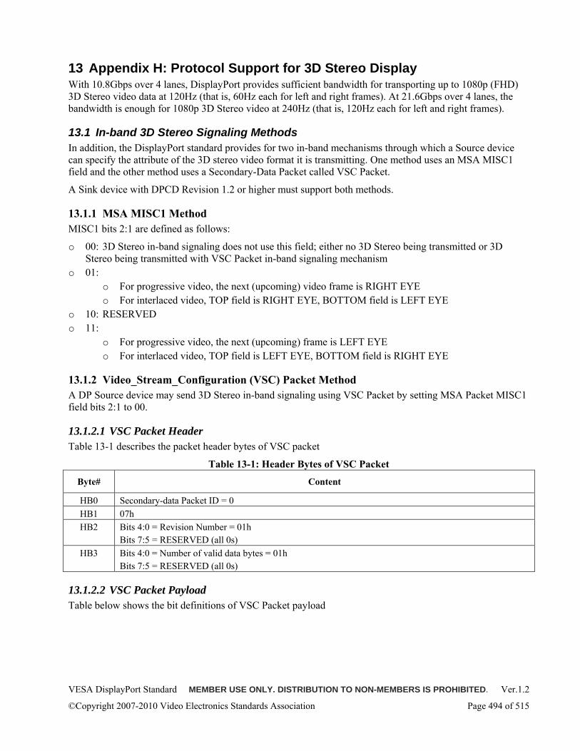
VESA DisplayPort Standard MEMBER USE ONLY. DISTRIBUTION TO NON-MEMBERS IS PROHIBITED. Ver.1.2
©Copyright 2007-2010 Video Electronics Standards Association Page 494 of 515
13 Appendix H: Protocol Support for 3D Stereo Display With 10.8Gbps over 4 lanes, DisplayPort provides sufficient bandwidth for transporting up to 1080p (FHD) 3D Stereo video data at 120Hz (that is, 60Hz each for left and right frames). At 21.6Gbps over 4 lanes, the bandwidth is enough for 1080p 3D Stereo video at 240Hz (that is, 120Hz each for left and right frames).
13.1 In-band 3D Stereo Signaling Methods In addition, the DisplayPort standard provides for two in-band mechanisms through which a Source device can specify the attribute of the 3D stereo video format it is transmitting. One method uses an MSA MISC1 field and the other method uses a Secondary-Data Packet called VSC Packet.
A Sink device with DPCD Revision 1.2 or higher must support both methods.
13.1.1 MSA MISC1 Method MISC1 bits 2:1 are defined as follows:
o 00: 3D Stereo in-band signaling does not use this field; either no 3D Stereo being transmitted or 3D Stereo being transmitted with VSC Packet in-band signaling mechanism
o 01: o For progressive video, the next (upcoming) video frame is RIGHT EYE o For interlaced video, TOP field is RIGHT EYE, BOTTOM field is LEFT EYE
o 10: RESERVED o 11:
o For progressive video, the next (upcoming) frame is LEFT EYE o For interlaced video, TOP field is LEFT EYE, BOTTOM field is RIGHT EYE
13.1.2 Video_Stream_Configuration (VSC) Packet Method A DP Source device may send 3D Stereo in-band signaling using VSC Packet by setting MSA Packet MISC1 field bits 2:1 to 00.
13.1.2.1 VSC Packet Header Table 13-1 describes the packet header bytes of VSC packet
Table 13-1: Header Bytes of VSC Packet
Byte# Content
HB0 Secondary-data Packet ID = 0 HB1 07h HB2 Bits 4:0 = Revision Number = 01h
Bits 7:5 = RESERVED (all 0s) HB3 Bits 4:0 = Number of valid data bytes = 01h
Bits 7:5 = RESERVED (all 0s)
13.1.2.2 VSC Packet Payload Table below shows the bit definitions of VSC Packet payload
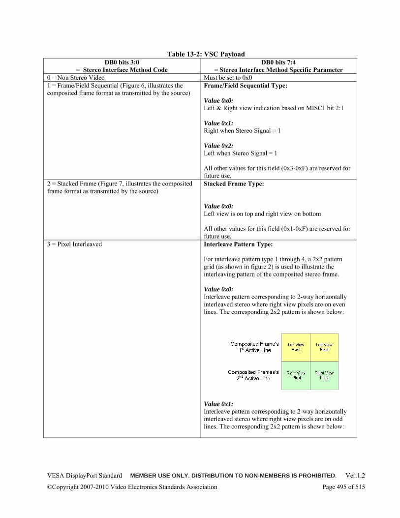
VESA DisplayPort Standard MEMBER USE ONLY. DISTRIBUTION TO NON-MEMBERS IS PROHIBITED. Ver.1.2
©Copyright 2007-2010 Video Electronics Standards Association Page 495 of 515
Table 13-2: VSC Payload DB0 bits 3:0
= Stereo Interface Method Code DB0 bits 7:4
= Stereo Interface Method Specific Parameter 0 = Non Stereo Video Must be set to 0x0 1 = Frame/Field Sequential (Figure 6, illustrates the composited frame format as transmitted by the source)
Frame/Field Sequential Type: Value 0x0: Left & Right view indication based on MISC1 bit 2:1 Value 0x1: Right when Stereo Signal = 1 Value 0x2: Left when Stereo Signal = 1 All other values for this field (0x3-0xF) are reserved for future use.
2 = Stacked Frame (Figure 7, illustrates the composited frame format as transmitted by the source)
Stacked Frame Type: Value 0x0: Left view is on top and right view on bottom All other values for this field (0x1-0xF) are reserved for future use.
3 = Pixel Interleaved
Interleave Pattern Type: For interleave pattern type 1 through 4, a 2x2 pattern grid (as shown in figure 2) is used to illustrate the interleaving pattern of the composited stereo frame. Value 0x0: Interleave pattern corresponding to 2-way horizontally interleaved stereo where right view pixels are on even lines. The corresponding 2x2 pattern is shown below:
Value 0x1: Interleave pattern corresponding to 2-way horizontally interleaved stereo where right view pixels are on odd lines. The corresponding 2x2 pattern is shown below:
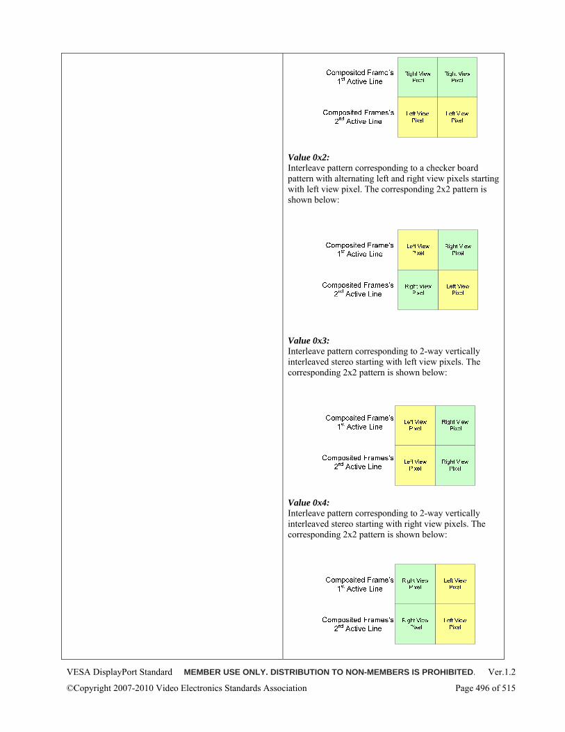
VESA DisplayPort Standard MEMBER USE ONLY. DISTRIBUTION TO NON-MEMBERS IS PROHIBITED. Ver.1.2
©Copyright 2007-2010 Video Electronics Standards Association Page 496 of 515
Value 0x2: Interleave pattern corresponding to a checker board pattern with alternating left and right view pixels starting with left view pixel. The corresponding 2x2 pattern is shown below:
Value 0x3: Interleave pattern corresponding to 2-way vertically interleaved stereo starting with left view pixels. The corresponding 2x2 pattern is shown below:
Value 0x4: Interleave pattern corresponding to 2-way vertically interleaved stereo starting with right view pixels. The corresponding 2x2 pattern is shown below:
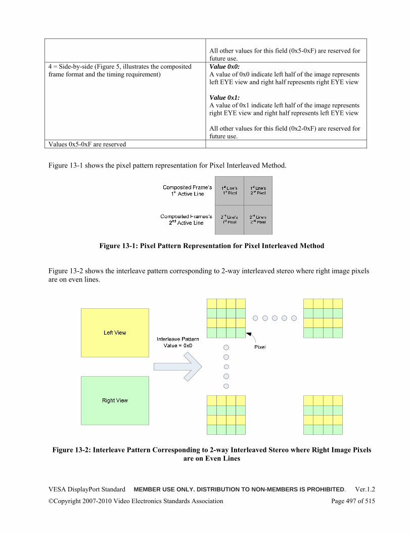
VESA DisplayPort Standard MEMBER USE ONLY. DISTRIBUTION TO NON-MEMBERS IS PROHIBITED. Ver.1.2
©Copyright 2007-2010 Video Electronics Standards Association Page 497 of 515
All other values for this field (0x5-0xF) are reserved for future use.
4 = Side-by-side (Figure 5, illustrates the composited frame format and the timing requirement)
Value 0x0: A value of 0x0 indicate left half of the image represents left EYE view and right half represents right EYE view Value 0x1: A value of 0x1 indicate left half of the image represents right EYE view and right half represents left EYE view All other values for this field (0x2-0xF) are reserved for future use.
Values 0x5-0xF are reserved
Figure 13-1 shows the pixel pattern representation for Pixel Interleaved Method.
Figure 13-1: Pixel Pattern Representation for Pixel Interleaved Method
Figure 13-2 shows the interleave pattern corresponding to 2-way interleaved stereo where right image pixels are on even lines.
Figure 13-2: Interleave Pattern Corresponding to 2-way Interleaved Stereo where Right Image Pixels
are on Even Lines
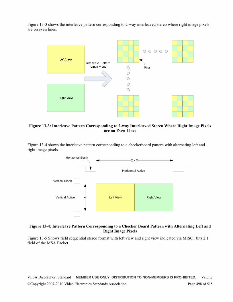
VESA DisplayPort Standard MEMBER USE ONLY. DISTRIBUTION TO NON-MEMBERS IS PROHIBITED. Ver.1.2
©Copyright 2007-2010 Video Electronics Standards Association Page 498 of 515
Figure 13-3 shows the interleave pattern corresponding to 2-way interleaved stereo where right image pixels are on even lines.
Figure 13-3: Interleave Pattern Corresponding to 2-way Interleaved Stereo Where Right Image Pixels
are on Even Lines
Figure 13-4 shows the interleave pattern corresponding to a checkerboard pattern with alternating left and right image pixels
2 x X
Left View Right ViewY
Horizontal Active
Horizontal Blank
Vertical Blank
Vertical Active
Figure 13-4: Interleave Pattern Corresponding to a Checker Board Pattern with Alternating Left and
Right Image Pixels
Figure 13-5 Shows field sequential stereo format with left view and right view indicated via MISC1 bits 2:1 field of the MSA Packet.
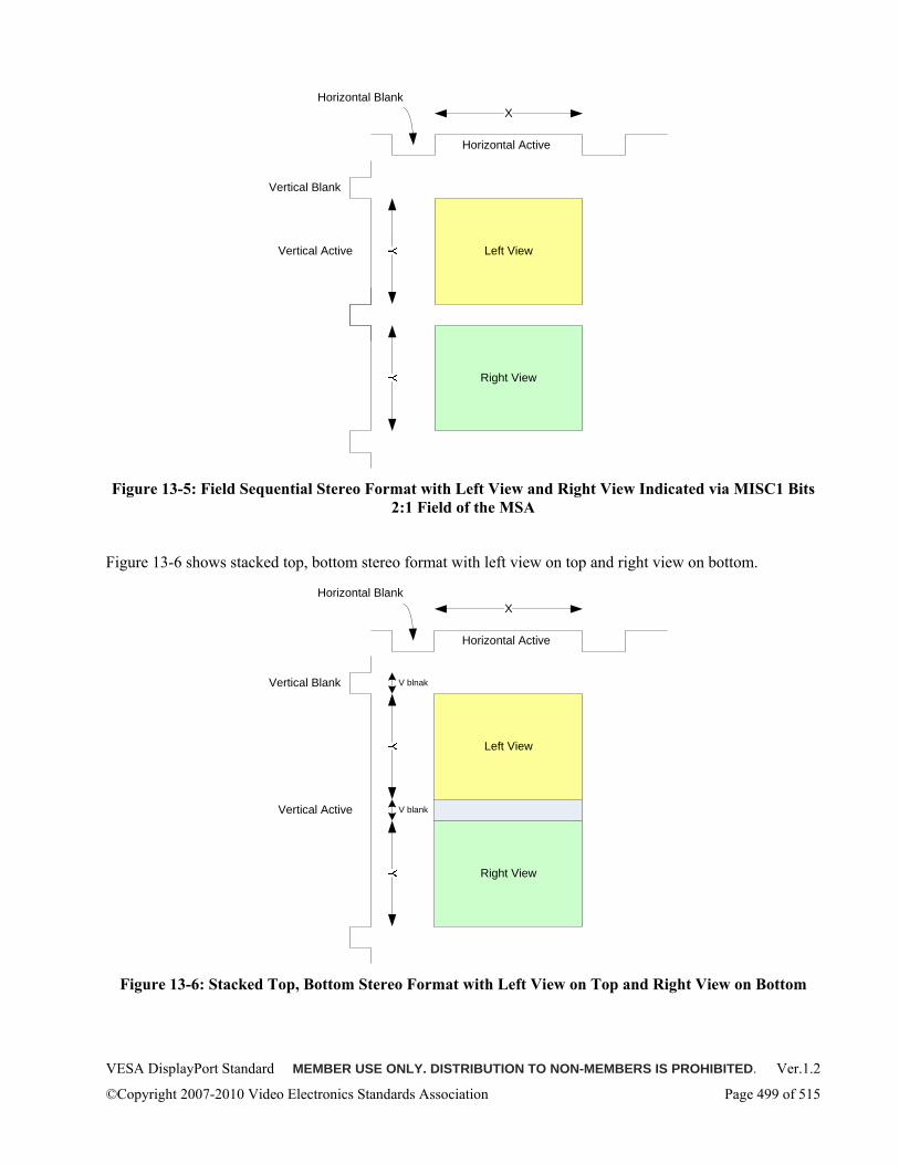
VESA DisplayPort Standard MEMBER USE ONLY. DISTRIBUTION TO NON-MEMBERS IS PROHIBITED. Ver.1.2
©Copyright 2007-2010 Video Electronics Standards Association Page 499 of 515
X
Left View
Right View
Horizontal Active
Horizontal Blank
Vertical Blank
Vertical Active
Figure 13-5: Field Sequential Stereo Format with Left View and Right View Indicated via MISC1 Bits
2:1 Field of the MSA
Figure 13-6 shows stacked top, bottom stereo format with left view on top and right view on bottom.
Left View
Right View
Vertical Blank
Vertical Active
X
Horizontal Active
Horizontal Blank
V blnak
V blank
Figure 13-6: Stacked Top, Bottom Stereo Format with Left View on Top and Right View on Bottom
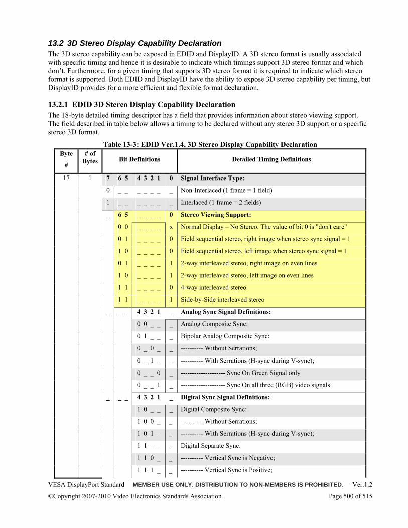
VESA DisplayPort Standard MEMBER USE ONLY. DISTRIBUTION TO NON-MEMBERS IS PROHIBITED. Ver.1.2
©Copyright 2007-2010 Video Electronics Standards Association Page 500 of 515
13.2 3D Stereo Display Capability Declaration The 3D stereo capability can be exposed in EDID and DisplayID. A 3D stereo format is usually associated with specific timing and hence it is desirable to indicate which timings support 3D stereo format and which don’t. Furthermore, for a given timing that supports 3D stereo format it is required to indicate which stereo format is supported. Both EDID and DisplayID have the ability to expose 3D stereo capability per timing, but DisplayID provides for a more efficient and flexible format declaration.
13.2.1 EDID 3D Stereo Display Capability Declaration The 18-byte detailed timing descriptor has a field that provides information about stereo viewing support. The field described in table below allows a timing to be declared without any stereo 3D support or a specific stereo 3D format.
Table 13-3: EDID Ver.1.4, 3D Stereo Display Capability Declaration Byte
#
# of Bytes Bit Definitions Detailed Timing Definitions
7 6 5 4 3 2 1 0 Signal Interface Type:
0 _ _ _ _ _ _ _ Non-Interlaced (1 frame = 1 field)
1 _ _ _ _ _ _ _ Interlaced (1 frame = 2 fields)
_ 6 5 _ _ _ _ 0 Stereo Viewing Support:
0 0 _ _ _ _ x Normal Display – No Stereo. The value of bit 0 is "don't care"
0 1 _ _ _ _ 0 Field sequential stereo, right image when stereo sync signal = 1
1 0 _ _ _ _ 0 Field sequential stereo, left image when stereo sync signal = 1
0 1 _ _ _ _ 1 2-way interleaved stereo, right image on even lines
1 0 _ _ _ _ 1 2-way interleaved stereo, left image on even lines
1 1 _ _ _ _ 0 4-way interleaved stereo
1 1 _ _ _ _ 1 Side-by-Side interleaved stereo
_ _ _ 4 3 2 1 _ Analog Sync Signal Definitions:
0 0 _ _ _ Analog Composite Sync:
0 1 _ _ _ Bipolar Analog Composite Sync:
0 _ 0 _ _ ---------- Without Serrations;
0 _ 1 _ _ ---------- With Serrations (H-sync during V-sync);
0 _ _ 0 _ -------------------- Sync On Green Signal only
0 _ _ 1 _ -------------------- Sync On all three (RGB) video signals
_ _ _ 4 3 2 1 _ Digital Sync Signal Definitions:
1 0 _ _ _ Digital Composite Sync:
1 0 0 _ _ ---------- Without Serrations;
1 0 1 _ _ ---------- With Serrations (H-sync during V-sync);
1 1 _ _ _ Digital Separate Sync:
1 1 0 _ _ ---------- Vertical Sync is Negative;
17 1
1 1 1 _ _ ---------- Vertical Sync is Positive;
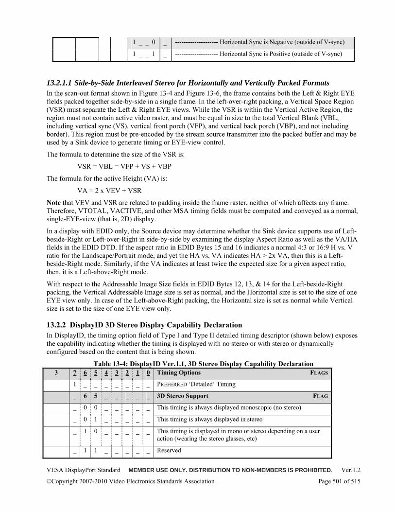
VESA DisplayPort Standard MEMBER USE ONLY. DISTRIBUTION TO NON-MEMBERS IS PROHIBITED. Ver.1.2
©Copyright 2007-2010 Video Electronics Standards Association Page 501 of 515
1 _ _ 0 _ -------------------- Horizontal Sync is Negative (outside of V-sync)
1 _ _ 1 _ -------------------- Horizontal Sync is Positive (outside of V-sync)
13.2.1.1 Side-by-Side Interleaved Stereo for Horizontally and Vertically Packed Formats In the scan-out format shown in Figure 13-4 and Figure 13-6, the frame contains both the Left & Right EYE fields packed together side-by-side in a single frame. In the left-over-right packing, a Vertical Space Region (VSR) must separate the Left & Right EYE views. While the VSR is within the Vertical Active Region, the region must not contain active video raster, and must be equal in size to the total Vertical Blank (VBL, including vertical sync (VS), vertical front porch (VFP), and vertical back porch (VBP), and not including border). This region must be pre-encoded by the stream source transmitter into the packed buffer and may be used by a Sink device to generate timing or EYE-view control.
The formula to determine the size of the VSR is:
VSR = VBL = VFP + VS + VBP
The formula for the active Height (VA) is:
VA = 2 x VEV + VSR
Note that VEV and VSR are related to padding inside the frame raster, neither of which affects any frame. Therefore, VTOTAL, VACTIVE, and other MSA timing fields must be computed and conveyed as a normal, single-EYE-view (that is, 2D) display.
In a display with EDID only, the Source device may determine whether the Sink device supports use of Left-beside-Right or Left-over-Right in side-by-side by examining the display Aspect Ratio as well as the VA/HA fields in the EDID DTD. If the aspect ratio in EDID Bytes 15 and 16 indicates a normal 4:3 or 16:9 H vs. V ratio for the Landscape/Portrait mode, and yet the HA vs. VA indicates HA > 2x VA, then this is a Left-beside-Right mode. Similarly, if the VA indicates at least twice the expected size for a given aspect ratio, then, it is a Left-above-Right mode.
With respect to the Addressable Image Size fields in EDID Bytes 12, 13, & 14 for the Left-beside-Right packing, the Vertical Addressable Image size is set as normal, and the Horizontal size is set to the size of one EYE view only. In case of the Left-above-Right packing, the Horizontal size is set as normal while Vertical size is set to the size of one EYE view only.
13.2.2 DisplayID 3D Stereo Display Capability Declaration In DisplayID, the timing option field of Type I and Type II detailed timing descriptor (shown below) exposes the capability indicating whether the timing is displayed with no stereo or with stereo or dynamically configured based on the content that is being shown.
Table 13-4: DisplayID Ver.1.1, 3D Stereo Display Capability Declaration 3 7 6 5 4 3 2 1 0 Timing Options FLAGS
1 _ _ _ _ _ _ _ PREFERRED ‘Detailed’ Timing
_ 6 5 _ _ _ _ _ 3D Stereo Support FLAG
_ 0 0 _ _ _ _ _ This timing is always displayed monoscopic (no stereo)
_ 0 1 _ _ _ _ _ This timing is always displayed in stereo
_ 1 0 _ _ _ _ _ This timing is displayed in mono or stereo depending on a user action (wearing the stereo glasses, etc)
_ 1 1 _ _ _ _ _ Reserved
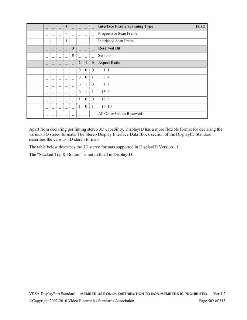
VESA DisplayPort Standard MEMBER USE ONLY. DISTRIBUTION TO NON-MEMBERS IS PROHIBITED. Ver.1.2
©Copyright 2007-2010 Video Electronics Standards Association Page 502 of 515
_ _ _ 4 _ _ _ _ Interface Frame Scanning Type FLAG
_ _ _ 0 _ _ _ _ Progressive Scan Frame
_ _ _ 1 _ _ _ _ Interlaced Scan Frame
_ _ _ _ 3 _ _ _ Reserved Bit
_ _ _ _ 0 _ _ _ Set to 0
_ _ _ _ _ 2 1 0 Aspect Ratio
_ _ _ _ _ 0 0 0 1: 1
_ _ _ _ _ 0 0 1 5: 4
_ _ _ _ _ 0 1 0 4: 3
_ _ _ _ _ 0 1 1 15: 9
_ _ _ _ _ 1 0 0 16: 9
_ _ _ _ _ 1 0 1 16: 10
_ _ _ _ _ _ _ _ All Other Values Reserved
Apart from declaring per timing stereo 3D capability, DisplayID has a more flexible format for declaring the various 3D stereo formats. The Stereo Display Interface Data Block section of the DisplayID Standard describes the various 3D stereo formats.
The table below describes the 3D stereo formats supported in DisplayID Version1.1.
The “Stacked Top & Bottom” is not defined in DisplayID.
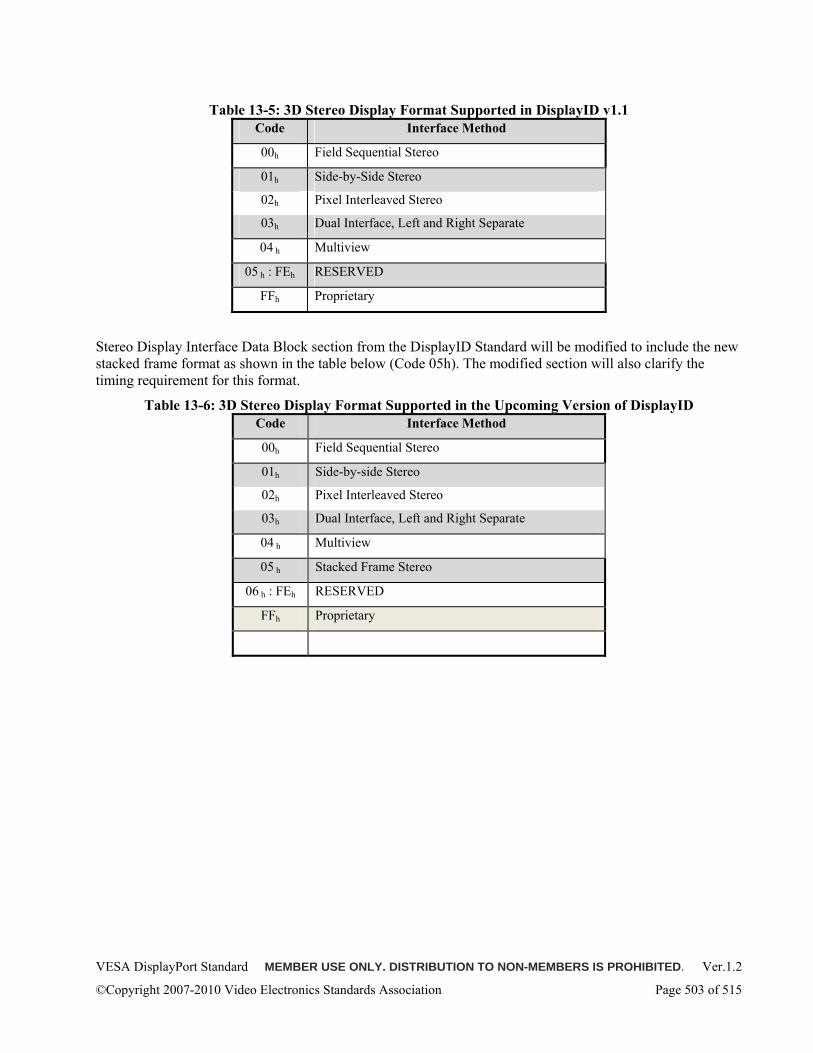
VESA DisplayPort Standard MEMBER USE ONLY. DISTRIBUTION TO NON-MEMBERS IS PROHIBITED. Ver.1.2
©Copyright 2007-2010 Video Electronics Standards Association Page 503 of 515
Table 13-5: 3D Stereo Display Format Supported in DisplayID v1.1 Code Interface Method
00h Field Sequential Stereo
01h Side-by-Side Stereo
02h Pixel Interleaved Stereo
03h Dual Interface, Left and Right Separate
04 h Multiview
05 h : FEh RESERVED
FFh Proprietary
Stereo Display Interface Data Block section from the DisplayID Standard will be modified to include the new stacked frame format as shown in the table below (Code 05h). The modified section will also clarify the timing requirement for this format.
Table 13-6: 3D Stereo Display Format Supported in the Upcoming Version of DisplayID Code Interface Method
00h Field Sequential Stereo
01h Side-by-side Stereo
02h Pixel Interleaved Stereo
03h Dual Interface, Left and Right Separate
04 h Multiview
05 h Stacked Frame Stereo
06 h : FEh RESERVED
FFh Proprietary
VESA DisplayPort Standard MEMBER USE ONLY. DISTRIBUTION TO NON-MEMBERS IS PROHIBITED. Ver.1.2
©Copyright 2007-2010 Video Electronics Standards Association Page 504 of 515
14 Appendix I: QUERY_STREAM_ENCRYPTION_STATUS MESSAGE TRANSACTION in a CP Tree Topology
Prior to the introduction MST transport format and MST topology features in the DisplayPort Standard, each of one or multiple DP display output ports was controlled by each transmitter of a Source device (such as a GPU), and the status of content on each display output port was known and controlled by the GPU.
Since the GPU is typically a “licensed source component” of Content Protection (CP) technology, it has been required to robustly convey the status of the CP protocols on those output ports to content players supporting approved output protection protocols. In an MST topology, however, the routing of content streams happen outside the GPU, typically via unsecured software control through insecure Sideband MSGs over AUX CH.
14.1 Self-checking by Branch Devices By CP license, Branch devices are likely to be required to apply a “Self-Checking” policy. Complying with the policy, Branch devices are to detect misconfigurations and apply license policy control directly, for example, by disabling an unauthenticated output port or by down sampling at the Branch device level, and reflect the success/failure to the upstream transmitter, for example, by aborting authentication upon failure.
The difficulty with Self-Checking at the Branch device level is that the policy varies among content licenses and CP technology. Some content licenses (DTCP, for example) prohibit the devices from interfering with the displaying of content (by disabling a display output port, for example), regardless if the authentication has been successfully established or not, when a “copy-always” policy is presented even when the content itself may be protected. Other licenses (AACS, for example) require the down-sampling of content when the attached display does not support the approved CP protocols.
14.2 Merit of QUERY_STREAM_ENCRYPTION_STATUS Message Transaction The QUERY_STREAM_ENCRYPTION_STATUS message transaction has the advantage of allowing the stream routing status to be robustly conveyed to the Source device of MST topology while keeping DisplayPort Standard agnostic of any particular CP protocol and/or policy.
CP-licensed Source component devices such as GPUs are responsible for indicating the presence of CP capable end-points and the Authentication/Revocation status to Content Player applications with the level of robustness required by the CP Licenses and additional API Licenses supporting Licensed Content.
As a usage model, it is desirable that the encryption state of independent output streams in an MST topology not affect the other output streams. For example, consider the scenario in which a non-CP device is hot plugged to an MST Branch device while the link driven by a Source device of the MST topology has already been authenticated and stream outputs from the Source device have been encrypted. In this usage scenario, it is desirable that the failure to authenticate a newly added, non-CP device not cause authentication to be aborted on unrelated stream outputs; such behavior would not be consistent with the behavior of a Source device outputting multiple display streams from multiple physical display output ports, or display connectors (that is, one display stream per display connector).
Conversely, when a CP-capable device is hot plugged to an MST Branch device and authentication succeeds, the input stream to the MST Branch device may enable encryption on the specific stream routed to the newly plugged CP-capable device, and this enablement of encryption to that specific stream output should not require unrelated output streams to become also encrypted.
An MST Branch device may be considered as the collection of multiple independent virtual repeater devices. CP policy must be applied to a repeater function of each stream output. To facilitate the authentication status of a stream output as discernible from its upstream (or parent) link state, QUERY_STREAM _ENCRYPTION_STATUS message transaction provides for this information on a per stream basis with robustness to a Source device.
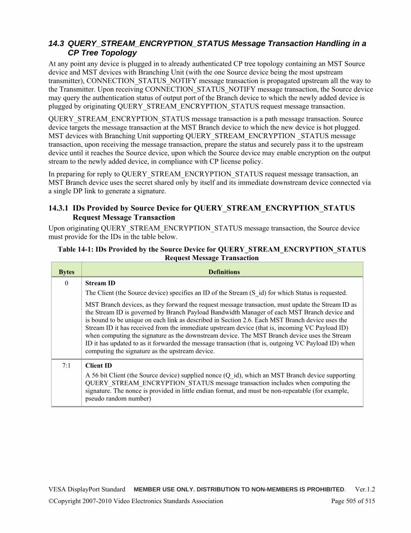
VESA DisplayPort Standard MEMBER USE ONLY. DISTRIBUTION TO NON-MEMBERS IS PROHIBITED. Ver.1.2
©Copyright 2007-2010 Video Electronics Standards Association Page 505 of 515
14.3 QUERY_STREAM_ENCRYPTION_STATUS Message Transaction Handling in a CP Tree Topology
At any point any device is plugged in to already authenticated CP tree topology containing an MST Source device and MST devices with Branching Unit (with the one Source device being the most upstream transmitter), CONNECTION_STATUS_NOTIFY message transaction is propagated upstream all the way to the Transmitter. Upon receiving CONNECTION_STATUS_NOTIFY message transaction, the Source device may query the authentication status of output port of the Branch device to which the newly added device is plugged by originating QUERY_STREAM_ENCRYPTION_STATUS request message transaction.
QUERY_STREAM_ENCRYPTION_STATUS message transaction is a path message transaction. Source device targets the message transaction at the MST Branch device to which the new device is hot plugged. MST devices with Branching Unit supporting QUERY_STREAM_ENCRYPTION _STATUS message transaction, upon receiving the message transaction, prepare the status and securely pass it to the upstream device until it reaches the Source device, upon which the Source device may enable encryption on the output stream to the newly added device, in compliance with CP license policy.
In preparing for reply to QUERY_STREAM_ENCRYPTION_STATUS request message transaction, an MST Branch device uses the secret shared only by itself and its immediate downstream device connected via a single DP link to generate a signature.
14.3.1 IDs Provided by Source Device for QUERY_STREAM_ENCRYPTION_STATUS Request Message Transaction
Upon originating QUERY_STREAM_ENCRYPTION_STATUS message transaction, the Source device must provide for the IDs in the table below.
Table 14-1: IDs Provided by the Source Device for QUERY_STREAM_ENCRYPTION_STATUS Request Message Transaction
Bytes Definitions
0 Stream ID The Client (the Source device) specifies an ID of the Stream (S_id) for which Status is requested.
MST Branch devices, as they forward the request message transaction, must update the Stream ID as the Stream ID is governed by Branch Payload Bandwidth Manager of each MST Branch device and is bound to be unique on each link as described in Section 2.6. Each MST Branch device uses the Stream ID it has received from the immediate upstream device (that is, incoming VC Payload ID) when computing the signature as the downstream device. The MST Branch device uses the Stream ID it has updated to as it forwarded the message transaction (that is, outgoing VC Payload ID) when computing the signature as the upstream device.
7:1 Client ID A 56 bit Client (the Source device) supplied nonce (Q_id), which an MST Branch device supporting QUERY_STREAM_ENCRYPTION_STATUS message transaction includes when computing the signature. The nonce is provided in little endian format, and must be non-repeatable (for example, pseudo random number)
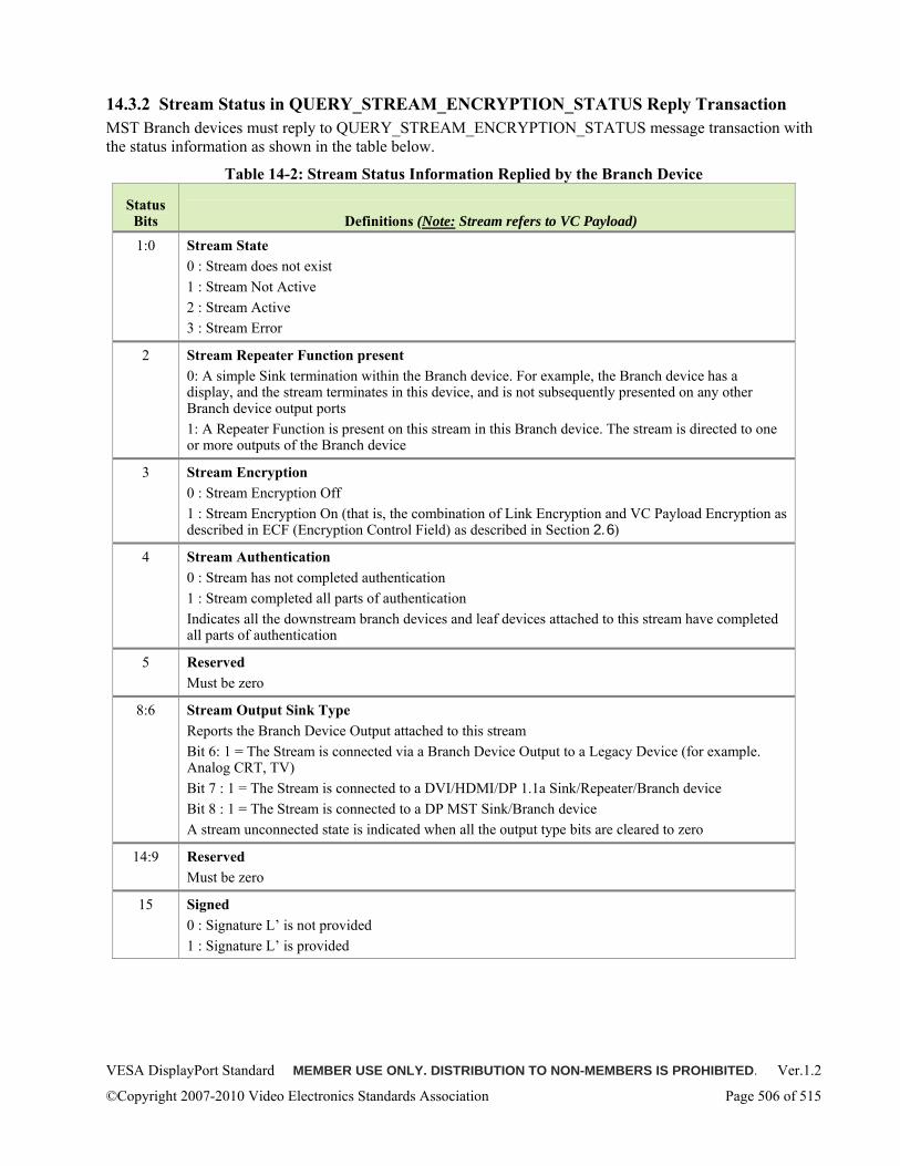
VESA DisplayPort Standard MEMBER USE ONLY. DISTRIBUTION TO NON-MEMBERS IS PROHIBITED. Ver.1.2
©Copyright 2007-2010 Video Electronics Standards Association Page 506 of 515
14.3.2 Stream Status in QUERY_STREAM_ENCRYPTION_STATUS Reply Transaction MST Branch devices must reply to QUERY_STREAM_ENCRYPTION_STATUS message transaction with the status information as shown in the table below.
Table 14-2: Stream Status Information Replied by the Branch Device
Status Bits Definitions (Note: Stream refers to VC Payload)
1:0 Stream State 0 : Stream does not exist 1 : Stream Not Active 2 : Stream Active 3 : Stream Error
2 Stream Repeater Function present 0: A simple Sink termination within the Branch device. For example, the Branch device has a display, and the stream terminates in this device, and is not subsequently presented on any other Branch device output ports 1: A Repeater Function is present on this stream in this Branch device. The stream is directed to one or more outputs of the Branch device
3 Stream Encryption 0 : Stream Encryption Off 1 : Stream Encryption On (that is, the combination of Link Encryption and VC Payload Encryption as described in ECF (Encryption Control Field) as described in Section 2.6)
4 Stream Authentication 0 : Stream has not completed authentication 1 : Stream completed all parts of authentication Indicates all the downstream branch devices and leaf devices attached to this stream have completed all parts of authentication
5 Reserved Must be zero
8:6 Stream Output Sink Type Reports the Branch Device Output attached to this stream Bit 6: 1 = The Stream is connected via a Branch Device Output to a Legacy Device (for example. Analog CRT, TV) Bit 7 : 1 = The Stream is connected to a DVI/HDMI/DP 1.1a Sink/Repeater/Branch device Bit 8 : 1 = The Stream is connected to a DP MST Sink/Branch device A stream unconnected state is indicated when all the output type bits are cleared to zero
14:9 Reserved Must be zero
15 Signed 0 : Signature L’ is not provided 1 : Signature L’ is provided
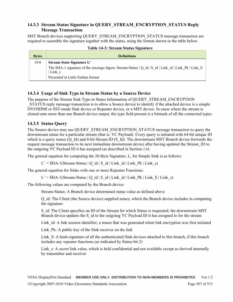
VESA DisplayPort Standard MEMBER USE ONLY. DISTRIBUTION TO NON-MEMBERS IS PROHIBITED. Ver.1.2
©Copyright 2007-2010 Video Electronics Standards Association Page 507 of 515
14.3.3 Stream Status Signature in QUERY_STREAM_ENCRYPTION_STATUS Reply Message Transaction
MST Branch devices supporting QUERY_STREAM_ENCRYPTION_STATUS message transaction are required to assemble the signature together with the status, using the format shown in the table below.
Table 14-3: Stream Status Signature
Bytes Definitions
19:0 Stream State Signature L’ The SHA-1 signature of the message digest: Stream-Status | Q_id | S_id | Link_id | Link_Pk | Link_S | Link_s Presented in Little Endian format
14.3.4 Usage of Sink Type in Stream Status by a Source Device The purpose of the Stream Sink Type in Status Information of QUERY_STREAM_ENCRYPTION _STATUS reply message transaction is to allow a Source device to identify if the attached device is a simple DVI/HDMI or SST-mode Sink device or Repeater device, or a MST device. In cases where the stream is cloned onto more than one Branch device output, the type field present is a bitmask of all the connected types.
14.3.5 Status Query The Source device may use QUERY_STREAM_ENCRYPTION_STATUS message transaction to query the downstream status for a particular stream (that is, VC Payload). Every query is initiated with 64-bit unique ID which is a query nonce (Q_Id) and 8-bit Stream ID (S_Id). The downstream MST Branch device forwards the request message transaction to its next immediate downstream device after having updated the Stream_ID to the outgoing VC Payload ID it has assigned (as described in Section 2.6).
The general equation for computing the 20-Byte Signature, L, for Simple Sink is as follows:
L’ = SHA-1(Stream-Status | Q_id | S_id | Link_id | Link_Pk | Link_s)
The general equation for Sinks with one or more Repeater Functions:
L’ = SHA-1(Stream-Status | Q_id | S_id | Link_id | Link_Pk | Link_S | Link_s)
The following values are computed by the Branch device:
Stream-Status: A Branch device determined status value as defined above
Q_id: The Client (the Source device) supplied nonce, which the Branch device includes in computing the signature
S_id: The Client specifies an ID of the Stream for which Status is requested; the downstream MST Branch device updates the S_id to the outgoing VC Payload ID it has assigned to for the stream
Link_id: A link session identifier, a nonce that was generated when link encryption was first initiated
Link_Pk: A public key of the Sink receiver on the link
Link_S: A hash-signature of all the authenticated Sink devices attached to this branch, if this branch includes any repeater functions (as indicated by Status bit 2)
Link_s: A secret link value, which is held confidential and not available except as derived internally by transmitter and receiver
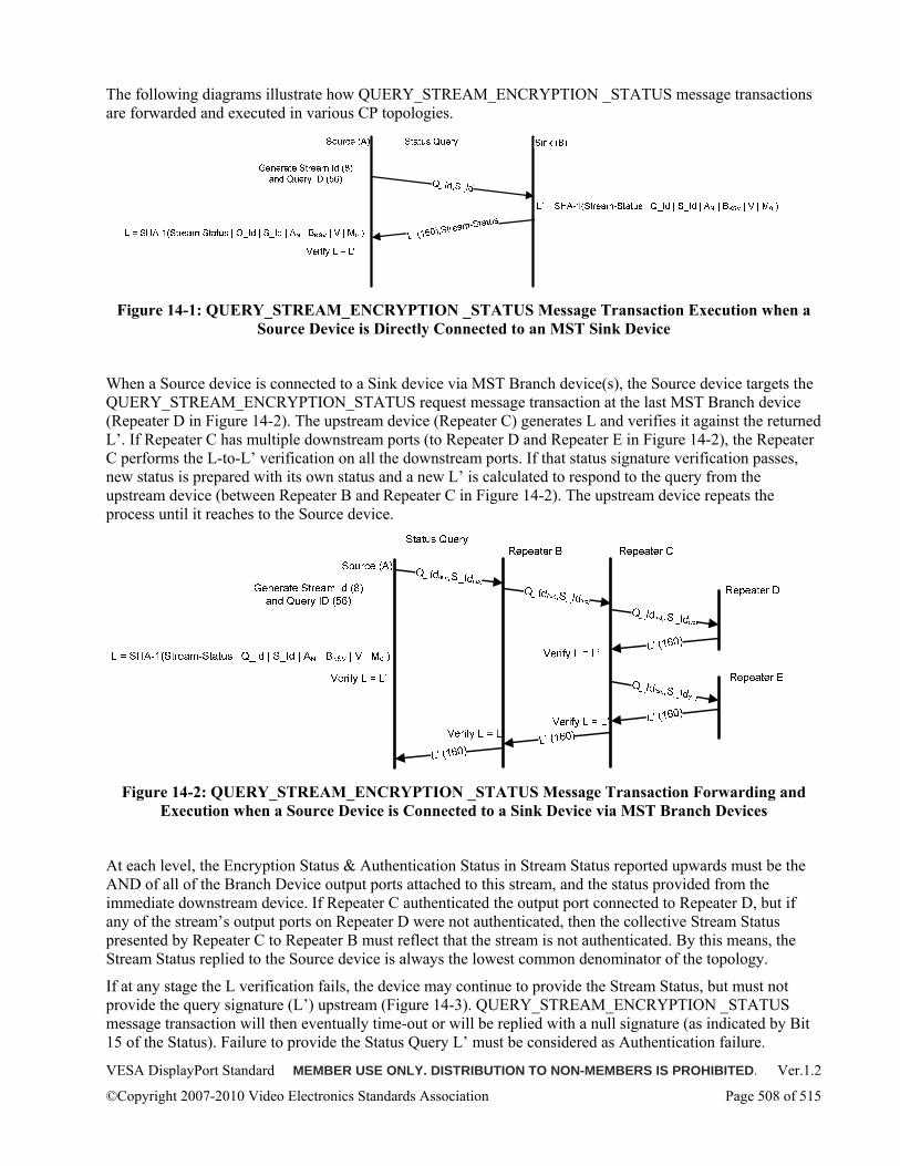
VESA DisplayPort Standard MEMBER USE ONLY. DISTRIBUTION TO NON-MEMBERS IS PROHIBITED. Ver.1.2
©Copyright 2007-2010 Video Electronics Standards Association Page 508 of 515
The following diagrams illustrate how QUERY_STREAM_ENCRYPTION _STATUS message transactions are forwarded and executed in various CP topologies.
Figure 14-1: QUERY_STREAM_ENCRYPTION _STATUS Message Transaction Execution when a
Source Device is Directly Connected to an MST Sink Device
When a Source device is connected to a Sink device via MST Branch device(s), the Source device targets the QUERY_STREAM_ENCRYPTION_STATUS request message transaction at the last MST Branch device (Repeater D in Figure 14-2). The upstream device (Repeater C) generates L and verifies it against the returned L’. If Repeater C has multiple downstream ports (to Repeater D and Repeater E in Figure 14-2), the Repeater C performs the L-to-L’ verification on all the downstream ports. If that status signature verification passes, new status is prepared with its own status and a new L’ is calculated to respond to the query from the upstream device (between Repeater B and Repeater C in Figure 14-2). The upstream device repeats the process until it reaches to the Source device.
Figure 14-2: QUERY_STREAM_ENCRYPTION _STATUS Message Transaction Forwarding and
Execution when a Source Device is Connected to a Sink Device via MST Branch Devices
At each level, the Encryption Status & Authentication Status in Stream Status reported upwards must be the AND of all of the Branch Device output ports attached to this stream, and the status provided from the immediate downstream device. If Repeater C authenticated the output port connected to Repeater D, but if any of the stream’s output ports on Repeater D were not authenticated, then the collective Stream Status presented by Repeater C to Repeater B must reflect that the stream is not authenticated. By this means, the Stream Status replied to the Source device is always the lowest common denominator of the topology.
If at any stage the L verification fails, the device may continue to provide the Stream Status, but must not provide the query signature (L’) upstream (Figure 14-3). QUERY_STREAM_ENCRYPTION _STATUS message transaction will then eventually time-out or will be replied with a null signature (as indicated by Bit 15 of the Status). Failure to provide the Status Query L’ must be considered as Authentication failure.
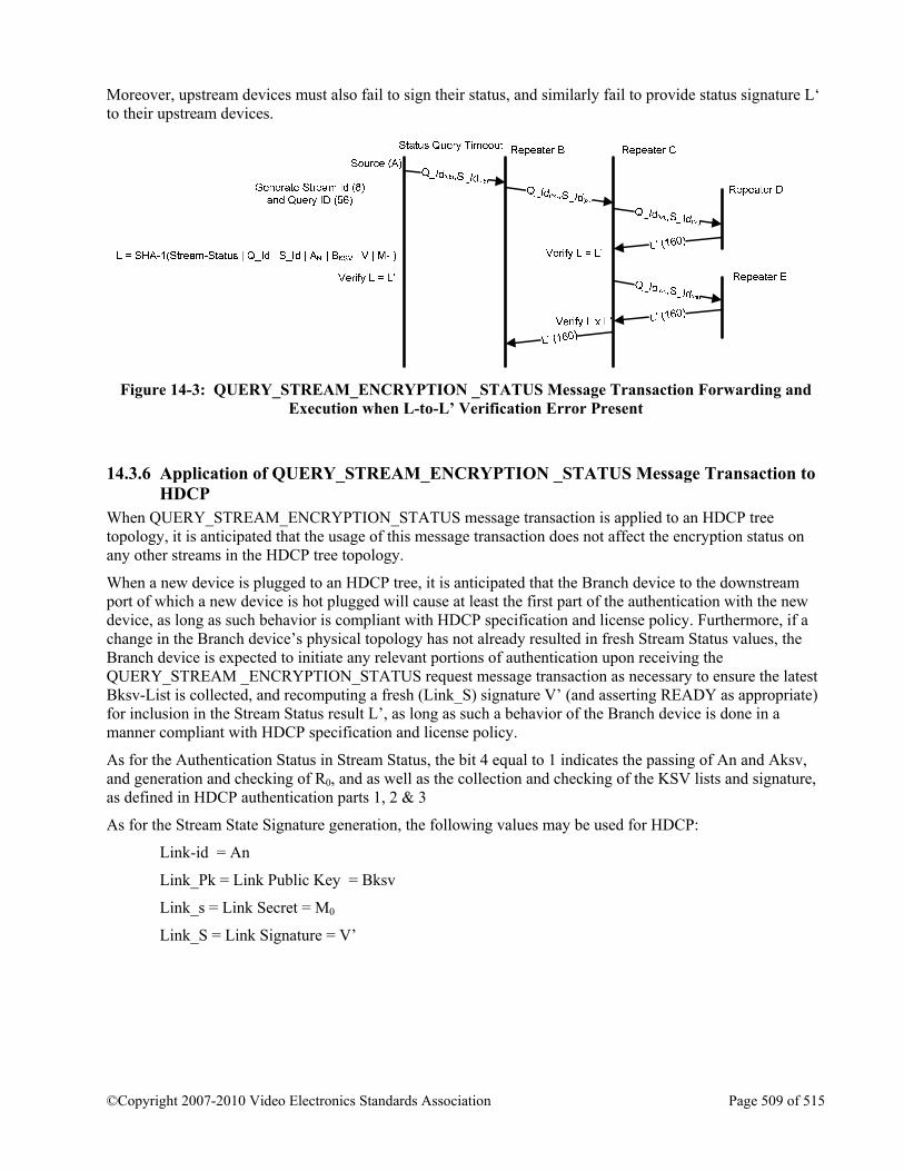
VESA DisplayPort Standard MEMBER USE ONLY. DISTRIBUTION TO NON-MEMBERS IS PROHIBITED. Ver.1.2
©Copyright 2007-2010 Video Electronics Standards Association Page 509 of 515
Moreover, upstream devices must also fail to sign their status, and similarly fail to provide status signature L‘ to their upstream devices.
Figure 14-3: QUERY_STREAM_ENCRYPTION _STATUS Message Transaction Forwarding and
Execution when L-to-L’ Verification Error Present
14.3.6 Application of QUERY_STREAM_ENCRYPTION _STATUS Message Transaction to HDCP
When QUERY_STREAM_ENCRYPTION_STATUS message transaction is applied to an HDCP tree topology, it is anticipated that the usage of this message transaction does not affect the encryption status on any other streams in the HDCP tree topology.
When a new device is plugged to an HDCP tree, it is anticipated that the Branch device to the downstream port of which a new device is hot plugged will cause at least the first part of the authentication with the new device, as long as such behavior is compliant with HDCP specification and license policy. Furthermore, if a change in the Branch device’s physical topology has not already resulted in fresh Stream Status values, the Branch device is expected to initiate any relevant portions of authentication upon receiving the QUERY_STREAM _ENCRYPTION_STATUS request message transaction as necessary to ensure the latest Bksv-List is collected, and recomputing a fresh (Link_S) signature V’ (and asserting READY as appropriate) for inclusion in the Stream Status result L’, as long as such a behavior of the Branch device is done in a manner compliant with HDCP specification and license policy.
As for the Authentication Status in Stream Status, the bit 4 equal to 1 indicates the passing of An and Aksv, and generation and checking of R0, and as well as the collection and checking of the KSV lists and signature, as defined in HDCP authentication parts 1, 2 & 3
As for the Stream State Signature generation, the following values may be used for HDCP:
Link-id = An
Link_Pk = Link Public Key = Bksv
Link_s = Link Secret = M0
Link_S = Link Signature = V’
VESA DisplayPort Standard MEMBER USE ONLY. DISTRIBUTION TO NON-MEMBERS IS PROHIBITED. Ver.1.2
©Copyright 2007-2010 Video Electronics Standards Association Page 510 of 515
15 Appendix J: DisplayPort Power (Informative) Some DisplayPort subsystems, such as after-market add-in graphics cards, may have low-cost implementations of the over-current protection circuitry, and be built to assumptions concerning the 3.3V rail supplied to the cards that may not always hold for the systems in which they are used. Consequently, it may not always be possible to guarantee that these subsystems meet the DisplayPort DP_PWR specification for power providers. In the interests of maximizing interoperability, DisplayPort devices that consume DP_PWR are recommended to be designed to be tolerant to 2.85V on DP_PWR.
VESA DisplayPort Standard MEMBER USE ONLY. DISTRIBUTION TO NON-MEMBERS IS PROHIBITED. Ver.1.2
©Copyright 2007-2010 Video Electronics Standards Association Page 511 of 515
16 Main Contributor History (Previous Versions)
Table 16-1: Main Contributors to Version 1.0
Name Company
Jianbin Hao Analogix Semiconductor Craig Wiley Analogix Semiconductor Ning Zhu Analogix Semiconductor Richard Fung ATI Technologies David Glen ATI Technologies Jim Goodman ATI Technologies Betty Luk ATI Technologies Mazen Salloum ATI Technologies Christopher Pasqualino Broadcom Jeffrey C. Dunnihoo California Micro Devices Joe Giannuzzi Dell Joe Goodart Dell Bruce Montag Dell Task Group Chair Lee Mohrmann Dell Jim Webb Display Labs Alan Kobayashi Genesis Microchip Task Group Editor Ali Noorbakhsh Genesis Microchip Larry Prather Genesis Microchip Bob Myers Hewlett-Packard Task Group Vice-chair Jory Olson InFocus Ron Muir JAE Mark Saubert JAE Toshio Shimoyama JAE Gang Sun Lattice Semiconductor Vincent Lin Molex Scott Sommers Molex Jason Squire Molex William Tsu NVIDIA Jimmy Chiu Parade Technologies Jack Zhao Parade Technologies Marc Vauclair Philips Glenn Adler Philips Michael Epstein Philips Patrick Yu Philips George Wiley Qualcomm Ian Miller Samsung Information Systems America Yohei Ishizone THine Jun Okamura THine Doron Lapidot Tyco Electronics Jim Leidy Tyco Electronics Alain d’Hautecourt ViewSonic Hank Blauvelt Xponent Photonics
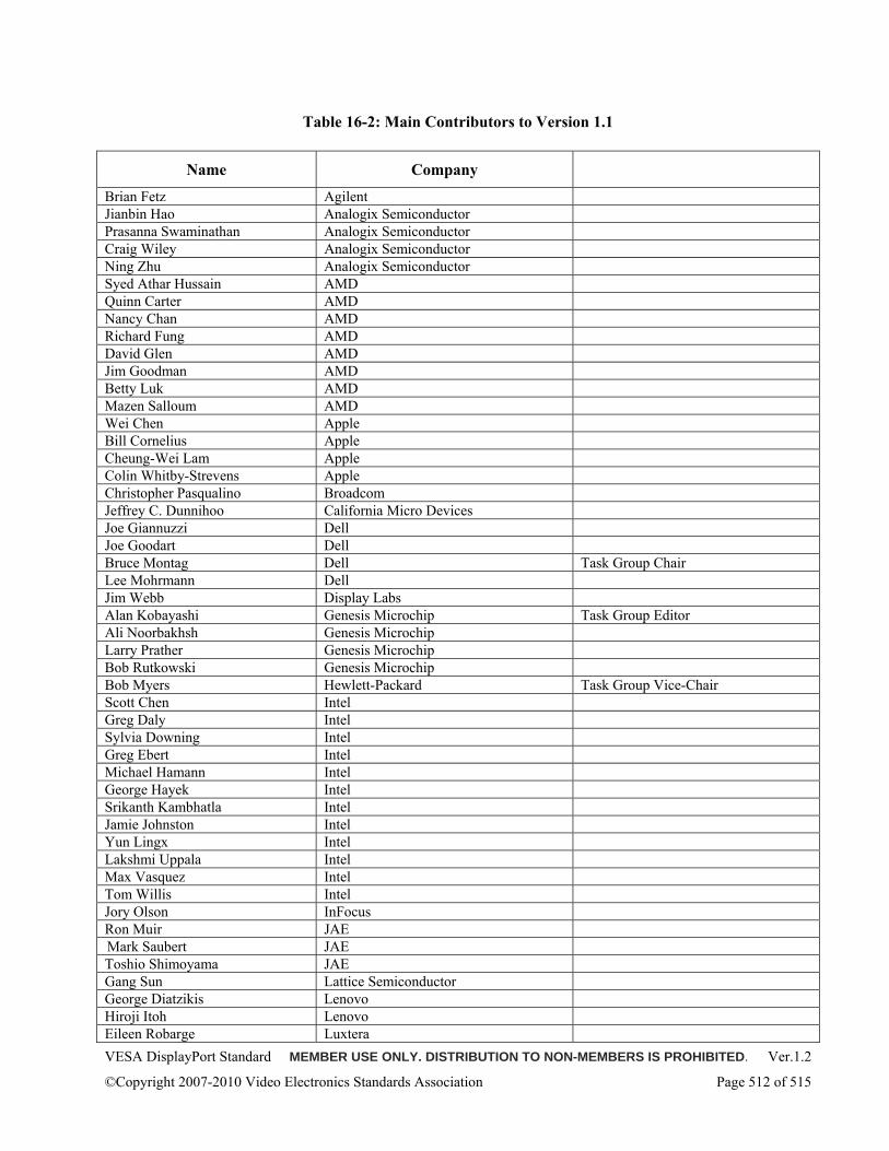
VESA DisplayPort Standard MEMBER USE ONLY. DISTRIBUTION TO NON-MEMBERS IS PROHIBITED. Ver.1.2
©Copyright 2007-2010 Video Electronics Standards Association Page 512 of 515
Table 16-2: Main Contributors to Version 1.1
Name Company
Brian Fetz Agilent Jianbin Hao Analogix Semiconductor Prasanna Swaminathan Analogix Semiconductor Craig Wiley Analogix Semiconductor Ning Zhu Analogix Semiconductor Syed Athar Hussain AMD Quinn Carter AMD Nancy Chan AMD Richard Fung AMD David Glen AMD Jim Goodman AMD Betty Luk AMD Mazen Salloum AMD Wei Chen Apple Bill Cornelius Apple Cheung-Wei Lam Apple Colin Whitby-Strevens Apple Christopher Pasqualino Broadcom Jeffrey C. Dunnihoo California Micro Devices Joe Giannuzzi Dell Joe Goodart Dell Bruce Montag Dell Task Group Chair Lee Mohrmann Dell Jim Webb Display Labs Alan Kobayashi Genesis Microchip Task Group Editor Ali Noorbakhsh Genesis Microchip Larry Prather Genesis Microchip Bob Rutkowski Genesis Microchip Bob Myers Hewlett-Packard Task Group Vice-Chair Scott Chen Intel Greg Daly Intel Sylvia Downing Intel Greg Ebert Intel Michael Hamann Intel George Hayek Intel Srikanth Kambhatla Intel Jamie Johnston Intel Yun Lingx Intel Lakshmi Uppala Intel Max Vasquez Intel Tom Willis Intel Jory Olson InFocus Ron Muir JAE Mark Saubert JAE Toshio Shimoyama JAE Gang Sun Lattice Semiconductor George Diatzikis Lenovo Hiroji Itoh Lenovo Eileen Robarge Luxtera
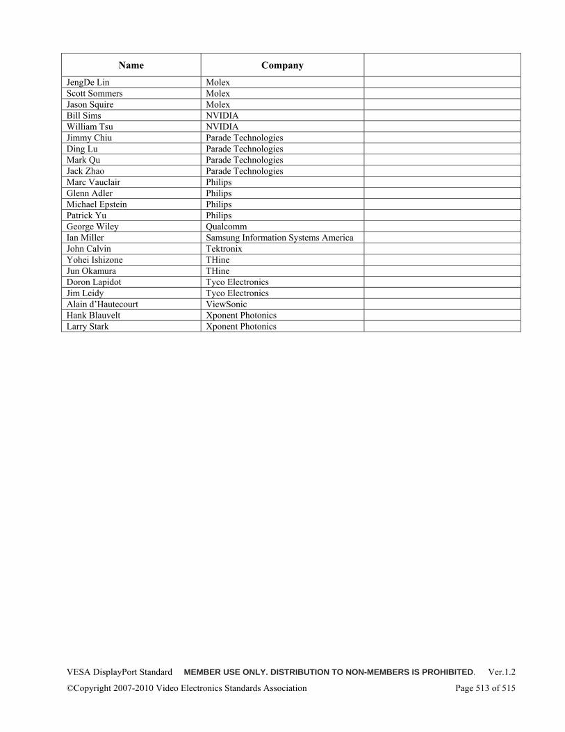
VESA DisplayPort Standard MEMBER USE ONLY. DISTRIBUTION TO NON-MEMBERS IS PROHIBITED. Ver.1.2
©Copyright 2007-2010 Video Electronics Standards Association Page 513 of 515
Name Company
JengDe Lin Molex Scott Sommers Molex Jason Squire Molex Bill Sims NVIDIA William Tsu NVIDIA Jimmy Chiu Parade Technologies Ding Lu Parade Technologies Mark Qu Parade Technologies Jack Zhao Parade Technologies Marc Vauclair Philips Glenn Adler Philips Michael Epstein Philips Patrick Yu Philips George Wiley Qualcomm Ian Miller Samsung Information Systems America John Calvin Tektronix Yohei Ishizone THine Jun Okamura THine Doron Lapidot Tyco Electronics Jim Leidy Tyco Electronics Alain d’Hautecourt ViewSonic Hank Blauvelt Xponent Photonics Larry Stark Xponent Photonics
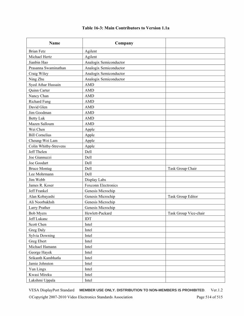
VESA DisplayPort Standard MEMBER USE ONLY. DISTRIBUTION TO NON-MEMBERS IS PROHIBITED. Ver.1.2
©Copyright 2007-2010 Video Electronics Standards Association Page 514 of 515
Table 16-3: Main Contributors to Version 1.1a
Name Company
Brian Fetz Agilent Michael Hertz Agilent Jianbin Hao Analogix Semiconductor Prasanna Swaminathan Analogix Semiconductor Craig Wiley Analogix Semiconductor Ning Zhu Analogix Semiconductor Syed Athar Hussain AMD Quinn Carter AMD Nancy Chan AMD Richard Fung AMD David Glen AMD Jim Goodman AMD Betty Luk AMD Mazen Salloum AMD Wei Chen Apple Bill Cornelius Apple Cheung-Wei Lam Apple Colin Whitby-Strevens Apple Jeff Thelen Dell Joe Giannuzzi Dell Joe Goodart Dell Bruce Montag Dell Task Group Chair Lee Mohrmann Dell Jim Webb Display Labs James R. Koser Foxconn Electronics Jeff Frankel Genesis Microchip Alan Kobayashi Genesis Microchip Task Group Editor Ali Noorbakhsh Genesis Microchip Larry Prather Genesis Microchip Bob Myers Hewlett-Packard Task Group Vice-chair Jeff Lukanc IDT Scott Chen Intel Greg Daly Intel Sylvia Downing Intel Greg Ebert Intel Michael Hamann Intel George Hayek Intel Srikanth Kambhatla Intel Jamie Johnston Intel Yun Lingx Intel Kwasi Mireku Intel Lakshmi Uppala Intel
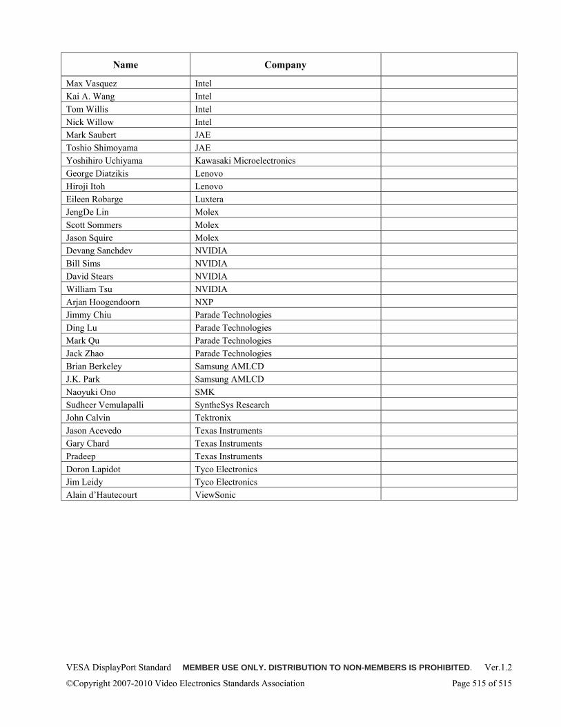
VESA DisplayPort Standard MEMBER USE ONLY. DISTRIBUTION TO NON-MEMBERS IS PROHIBITED. Ver.1.2
©Copyright 2007-2010 Video Electronics Standards Association Page 515 of 515
Name Company
Max Vasquez Intel Kai A. Wang Intel Tom Willis Intel Nick Willow Intel Mark Saubert JAE Toshio Shimoyama JAE Yoshihiro Uchiyama Kawasaki Microelectronics George Diatzikis Lenovo Hiroji Itoh Lenovo Eileen Robarge Luxtera JengDe Lin Molex Scott Sommers Molex Jason Squire Molex Devang Sanchdev NVIDIA Bill Sims NVIDIA David Stears NVIDIA William Tsu NVIDIA Arjan Hoogendoorn NXP Jimmy Chiu Parade Technologies Ding Lu Parade Technologies Mark Qu Parade Technologies Jack Zhao Parade Technologies Brian Berkeley Samsung AMLCD J.K. Park Samsung AMLCD Naoyuki Ono SMK Sudheer Vemulapalli SyntheSys Research John Calvin Tektronix Jason Acevedo Texas Instruments Gary Chard Texas Instruments Pradeep Texas Instruments Doron Lapidot Tyco Electronics Jim Leidy Tyco Electronics Alain d’Hautecourt ViewSonic