Embed Size (px)
Citation preview

January 2008 Rev 13 1/41
41
L4931ABxxL4931Cxx
Very low drop voltage regulators with inhibit
Features■ Very low dropout voltage (0.4 V)
■ Very low quiescent current
■ (Typ. 50 µA in off mode, 600 µA in on mode)
■ Output current up to 250 mA
■ Logic-controlled electronic shutdown
■ Output voltages of 1.5; 2.5; 2.7; 3.3; 3.5; 4.7; 5; 8; 12 V
■ Automotive Grade product: 2.7 V, 3.3 V, 3.5 V VOUT only in SO-8 package
■ Internal current and thermal limit
■ Only 2.2 µF for stability
■ Available in ± 1 % (AB) or 2 % (C) selection at 25 °C
■ Supply voltage rejection: 70 dB typ. for 5 V version
■ Temperature range: -40 to 125 °C
DescriptionThe L4931ABxx L4931Cxx are very Low Drop regulators available in TO-220, SO-8, DPAK, PPAK and TO-92 packages and in a wide range of output voltages.
The very low drop voltage (0.4 V) and the very low quiescent current make them particularly suitable for low noise, low power applications and specially in battery powered systems.
A TTL compatible shutdown logic control function is available in PPAK and SO-8 packages. This means that when the device is used as a local regulator, it is possible to put a part of the board in standby, decreasing the total power consumption. It requires only a 2.2 µF capacitor for stability allowing space and cost saving.
The L4931 is available as Automotive Grade in SO-8 package only, for the options of output voltages whose commercial Part Numbers are shown in the Table 24 (order codes). These devices are qualified according to the specification AEC-Q100 of the Automotive market, in the temperature range -40 °C to 125 °C, and the statistical tests PAT, SYL, SBL are performed.
TO-92
DPAK
TO-220
PPAK SO-8
Table 1. Device summary
Part number
L4931ABXX15 L4931CXX27 L4931CXX47 L4931ABXX120
L4931CXX15 L4931ABXX33 L4931ABXX50 L4931ABXX120
L4931ABXX25 L4931CXX33 L4931CXX50
L4931CXX25 L4931ABXX35 L4931ABXX80
L4931ABXX27 L4931CXX35 L4931CXX80
www.st.com
Contents L4931ABxx - L4931Cxx
2/41
Contents
1 Diagram . . . . . . . . . . . . . . . . . . . . . . . . . . . . . . . . . . . . . . . . . . . . . . . . . . . 3
2 Pin configuration . . . . . . . . . . . . . . . . . . . . . . . . . . . . . . . . . . . . . . . . . . . 4
3 Maximum ratings . . . . . . . . . . . . . . . . . . . . . . . . . . . . . . . . . . . . . . . . . . . . 5
4 Application circuits . . . . . . . . . . . . . . . . . . . . . . . . . . . . . . . . . . . . . . . . . 6
5 Electrical characteristics . . . . . . . . . . . . . . . . . . . . . . . . . . . . . . . . . . . . . 7
6 Typical application . . . . . . . . . . . . . . . . . . . . . . . . . . . . . . . . . . . . . . . . . 27
7 Package mechanical data . . . . . . . . . . . . . . . . . . . . . . . . . . . . . . . . . . . . 28
8 Order codes . . . . . . . . . . . . . . . . . . . . . . . . . . . . . . . . . . . . . . . . . . . . . . 37
9 Revision history . . . . . . . . . . . . . . . . . . . . . . . . . . . . . . . . . . . . . . . . . . . 38

L4931ABxx - L4931Cxx List of figures
3/41
List of figures
Figure 1. Schematic diagram . . . . . . . . . . . . . . . . . . . . . . . . . . . . . . . . . . . . . . . . . . . . . . . . . . . . . . . . 4Figure 2. Pin connections (top view) . . . . . . . . . . . . . . . . . . . . . . . . . . . . . . . . . . . . . . . . . . . . . . . . . . 5Figure 3. Test circuits. . . . . . . . . . . . . . . . . . . . . . . . . . . . . . . . . . . . . . . . . . . . . . . . . . . . . . . . . . . . . . 7Figure 4. Line regulation vs temperature . . . . . . . . . . . . . . . . . . . . . . . . . . . . . . . . . . . . . . . . . . . . . . 28Figure 5. Dropout voltage vs temperature . . . . . . . . . . . . . . . . . . . . . . . . . . . . . . . . . . . . . . . . . . . . . 28Figure 6. Supply current vs input voltage. . . . . . . . . . . . . . . . . . . . . . . . . . . . . . . . . . . . . . . . . . . . . . 28Figure 7. Supply current vs temperature . . . . . . . . . . . . . . . . . . . . . . . . . . . . . . . . . . . . . . . . . . . . . . 28Figure 8. Short circuit current vs dropout voltage . . . . . . . . . . . . . . . . . . . . . . . . . . . . . . . . . . . . . . . 29Figure 9. S.V.R. vs Input voltage signal frequency . . . . . . . . . . . . . . . . . . . . . . . . . . . . . . . . . . . . . . 29

List of tables L4931ABxx - L4931Cxx
4/41
List of tables
Table 1. Device summary . . . . . . . . . . . . . . . . . . . . . . . . . . . . . . . . . . . . . . . . . . . . . . . . . . . . . . . . . . 1Table 2. Absolute maximum ratings . . . . . . . . . . . . . . . . . . . . . . . . . . . . . . . . . . . . . . . . . . . . . . . . . . 7Table 3. Thermal data. . . . . . . . . . . . . . . . . . . . . . . . . . . . . . . . . . . . . . . . . . . . . . . . . . . . . . . . . . . . . 7Table 4. Electrical characteristics of L4931ABxx15 . . . . . . . . . . . . . . . . . . . . . . . . . . . . . . . . . . . . . . 9Table 5. Electrical characteristics of L4931Cxx15 . . . . . . . . . . . . . . . . . . . . . . . . . . . . . . . . . . . . . . 10Table 6. Electrical characteristics of L4931ABxx25 . . . . . . . . . . . . . . . . . . . . . . . . . . . . . . . . . . . . . 11Table 7. Electrical characteristics of L4931Cxx25 . . . . . . . . . . . . . . . . . . . . . . . . . . . . . . . . . . . . . . 12Table 8. Electrical characteristics of L4931ABxx27 . . . . . . . . . . . . . . . . . . . . . . . . . . . . . . . . . . . . . 13Table 9. Electrical characteristics of L4931Cxx27 . . . . . . . . . . . . . . . . . . . . . . . . . . . . . . . . . . . . . . 14Table 10. Electrical characteristics of L4931Cxx27-TRY (Automotive Grade) . . . . . . . . . . . . . . . . . . 15Table 11. Electrical characteristics of L4931ABxx33 . . . . . . . . . . . . . . . . . . . . . . . . . . . . . . . . . . . . . 16Table 12. Electrical characteristics of L4931Cxx33 . . . . . . . . . . . . . . . . . . . . . . . . . . . . . . . . . . . . . . 17Table 13. Electrical characteristics of L4931Cxx33-TRY (Automotive Grade) . . . . . . . . . . . . . . . . . . 18Table 14. Electrical characteristics of L4931ABxx35 . . . . . . . . . . . . . . . . . . . . . . . . . . . . . . . . . . . . . 19Table 15. Electrical characteristics of L4931ABxx35-TRY (Automotive Grade) . . . . . . . . . . . . . . . . . 20Table 16. Electrical characteristics of L4931Cxx35 . . . . . . . . . . . . . . . . . . . . . . . . . . . . . . . . . . . . . . 21Table 17. Electrical characteristics of L4931Cxx47 . . . . . . . . . . . . . . . . . . . . . . . . . . . . . . . . . . . . . . 22Table 18. Electrical characteristics of L4931ABxx50 . . . . . . . . . . . . . . . . . . . . . . . . . . . . . . . . . . . . . 23Table 19. Electrical characteristics of L4931Cxx50 . . . . . . . . . . . . . . . . . . . . . . . . . . . . . . . . . . . . . . 24Table 20. Electrical characteristics of L4931ABxx80 . . . . . . . . . . . . . . . . . . . . . . . . . . . . . . . . . . . . . 25Table 21. Electrical characteristics of L4931Cxx80 . . . . . . . . . . . . . . . . . . . . . . . . . . . . . . . . . . . . . . 26Table 22. Electrical characteristics of L4931ABxx120 . . . . . . . . . . . . . . . . . . . . . . . . . . . . . . . . . . . . 27Table 23. Electrical characteristics of L4931Cxx120 . . . . . . . . . . . . . . . . . . . . . . . . . . . . . . . . . . . . . 28Table 24. Order codes . . . . . . . . . . . . . . . . . . . . . . . . . . . . . . . . . . . . . . . . . . . . . . . . . . . . . . . . . . . . 39Table 25. Document revision history . . . . . . . . . . . . . . . . . . . . . . . . . . . . . . . . . . . . . . . . . . . . . . . . . 40
L4931ABxx - L4931Cxx Diagram
5/41
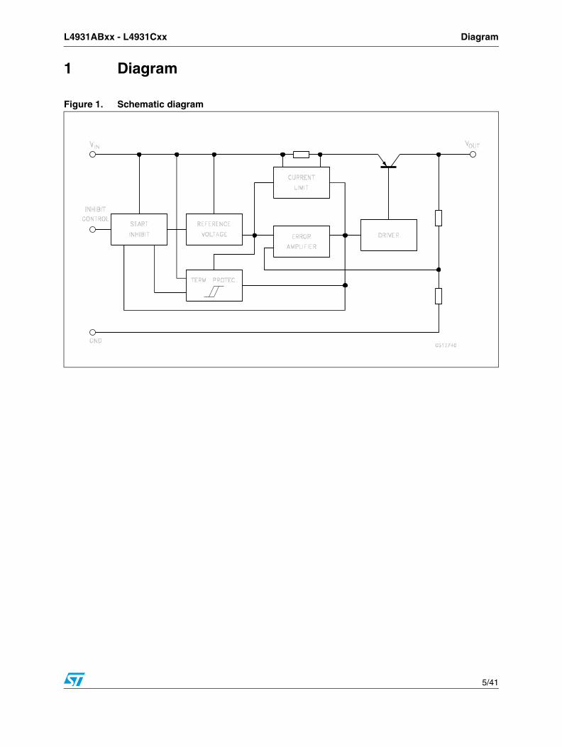
1 Diagram
Figure 1. Schematic diagram

Pin configuration L4931ABxx - L4931Cxx
6/41
2 Pin configuration
Figure 2. Pin connections (top view)
SO-8
DPAK
TO-220
PPAK
PIN 1 = VOUTPIN 2 = GNDPIN 3 = VIN
TO-92BOTTOM VIEW

L4931ABxx - L4931Cxx Maximum ratings
7/41
3 Maximum ratings
Note: Absolute maximum ratings are those values beyond which damage to the device may occur. Functional operation under these condition is not implied
Table 2. Absolute maximum ratings
Symbol Parameter Value Unit
VI DC Input voltage 20 V
IO Output current Internally limited mA
PD Power dissipation Internally limited mW
TSTG Storage temperature range -40 to 150 °C
TOP Operating junction temperature range -40 to 125 °C
Table 3. Thermal data
Symbol Parameter TO-220 SO-8 DPAK PPAK TO-92 Unit
RthJC Thermal resistance junction-case 3 20 8 8 °C/W
RthJA Thermal resistance junction-ambient 50 55 100 100 200 °C/W

Application circuits L4931ABxx - L4931Cxx
8/41
4 Application circuits
Figure 3. Test circuits

L4931ABxx - L4931Cxx Electrical characteristics
9/41
5 Electrical characteristics
Table 4. Electrical characteristics of L4931ABxx15 (refer to the test circuits, TA = 25 °C, CI = 0.1 µF, CO = 2.2 µF unless otherwise specified).
Symbol Parameter Test conditions Min. Typ. Max. Unit
VO Output voltageIO = 5 mA, VI = 3.5 V 1.485 1.5 1.515
VIO = 5 mA, VI = 3.5 V, TA=-25 to 85°C 1.47 1.53
VI Operating input voltage IO = 250 mA 2.5 20 V
Iout Output current limit 300 mA
ΔVO Line regulation VI = 2.5 to 20 V, IO = 0.5 mA 3 15 mV
ΔVO Load regulation (1)
1. For SO-8 package the maximum limit of load regulation and dropout is increased by 20 mV.
VI = 2.7 V, IO = 0.5 to 250 mA 3 15 mV
Id
Quiescent currentON MODE
VI = 2.7 to 20 V, IO = 0 mA 0.6 1mA
VI = 2.7 to 20 V, IO = 250 mA 4 6
OFF MODE VI = 6 V 50 100 µA
SVR Supply voltage rejectionIO = 5 mAVI = 3.7 ± 1 V
f = 120 Hz 79
dBf = 1 KHz 76
f = 10 KHz 55
eN Output noise voltage B = 10 Hz to 100 KHz 50 µV
Vd Dropout voltage (1) IO = 250 mA 1 V
VIL Control input logic low TA = -40 to 125°C 0.8 V
VIH Control Input Logic High TA = -40 to 125°C 2 V
II Control input current VI = 6 V, VC = 6 V 10 µA
COOutput bypass capacitance
ESR = 0.1 to 10 Ω, IO = 0 to 250 mA 2 10 µF

Electrical characteristics L4931ABxx - L4931Cxx
10/41
Table 5. Electrical characteristics of L4931Cxx15 (refer to the test circuits, TA = 25 °C,CI = 0.1 µF, CO = 2.2 µF unless otherwise specified).
Symbol Parameter Test conditions Min. Typ. Max. Unit
VO Output voltageIO = 5 mA, VI = 3.5 V 1.47 1.5 1.53
VIO = 5 mA, VI = 3.5 V, TA=-25 to 85°C 1.44 1.56
VI Operating input voltage IO = 250 mA 2.5 20 V
Iout Output current limit 300 mA
ΔVO Line regulation VI = 2.5 to 20 V, IO = 0.5 mA 3 18 mV
ΔVO Load regulation (1) VI = 2.7 V, IO = 0.5 to 250 mA 3 18 mV
Id
Quiescent currentON MODE
VI = 2.7 to 20 V, IO = 0 mA 0.6 1mA
VI = 2.7 to 20 V, IO = 250 mA 4 6
OFF MODE VI = 6 V 50 100 µA
SVR Supply voltage rejectionIO = 5 mAVI = 3.7 ± 1 V
f = 120 Hz 79
dBf = 1 KHz 76
f = 10 KHz 55
eN Output noise voltage B = 10 Hz to 100 KHz 50 µV
Vd Dropout voltage (1) IO = 250 mA 1 V
VIL Control input logic low TA = -40 to 125°C 0.8 V
VIH Control Input Logic High TA = -40 to 125°C 2 V
II Control input current VI = 6 V, VC = 6 V 10 µA
COOutput bypass capacitance
ESR = 0.1 to 10 Ω, IO = 0 to 250 mA 2 10 µF
1. For SO-8 package the maximum limit of load regulation and dropout is increased by 20 mV.

L4931ABxx - L4931Cxx Electrical characteristics
11/41
Table 6. Electrical characteristics of L4931ABxx25 (refer to the test circuits, TA = 25 °C, CI = 0.1 µF, CO = 2.2 µF unless otherwise specified).
Symbol Parameter Test conditions Min. Typ. Max. Unit
VO Output voltageIO = 5 mA, VI = 4.5 V 2.475 2.5 2.525
VIO = 5 mA, VI = 4.5 V, TA=-25 to 85°C 2.45 2.55
VI Operating input voltage IO = 250 mA 20 V
Iout Output current limit 300 mA
ΔVO Line regulation VI = 3.2 to 20 V, IO = 0.5 mA 3 15 mV
ΔVO Load regulation (1) VI = 3.4 V, IO = 0.5 to 250 mA 3 15 mV
Id
Quiescent currentON MODE
VI = 3.4 to 20 V, IO = 0 mA 0.6 1mA
VI = 3.4 to 20 V, IO = 250 mA 4 6
OFF MODE VI = 6 V 50 100 µA
SVR Supply voltage rejectionIO = 5 mAVI = 4.4 ± 1 V
f = 120 Hz 75
dBf = 1 KHz 72
f = 10 KHz 55
eN Output noise voltage B = 10 Hz to 100 KHz 50 µV
Vd Dropout voltage (1)IO = 250 mA 0.4 0.6 V
IO = 250 mA, TA= -40 to 125°C 0.8 V
VIL Control input logic low TA = -40 to 125°C 0.8 V
VIH Control Input Logic High TA = -40 to 125°C 2 V
II Control input current VI = 6 V, VC = 6 V 10 µA
COOutput bypass capacitance
ESR = 0.1 to 10 Ω, IO = 0 to 250 mA 2 10 µF
1. For SO-8 package the maximum limit of load regulation and dropout is increased by 20 mV.

Electrical characteristics L4931ABxx - L4931Cxx
12/41
Table 7. Electrical characteristics of L4931Cxx25 (refer to the test circuits, TA = 25 °C, CI = 0.1 µF, CO = 2.2 µF unless otherwise specified).
Symbol Parameter Test conditions Min. Typ. Max. Unit
VO Output voltageIO = 5 mA, VI = 4.5 V 2.45 2.5 2.55
VIO = 5 mA, VI = 4.5 V, TA=-25 to 85°C 2.4 2.6
VI Operating input voltage IO = 250 mA 20 V
Iout Output current limit 300 mA
ΔVO Line regulation VI = 3.3 to 20 V, IO = 0.5 mA 3 18 mV
ΔVO Load regulation (1) VI = 3.5 V, IO = 0.5 to 250 mA 3 18 mV
Id
Quiescent currentON MODE
VI = 3.5 to 20 V, IO = 0 mA 0.6 1mA
VI = 3.5 to 20 V, IO = 250 mA 4 6
OFF MODE VI = 6 V 50 100 µA
SVR Supply voltage rejectionIO = 5 mAVI = 4.4 ± 1 V
f = 120 Hz 75
dBf = 1 KHz 72
f = 10 KHz 55
eN Output noise voltage B = 10 Hz to 100 KHz 50 µV
Vd Dropout voltage (1)IO = 250 mA 0.4 0.6 V
IO = 250 mA, TA= -40 to 125°C 0.8 V
VIL Control input logic low TA = -40 to 125°C 0.8 V
VIH Control Input Logic High TA = -40 to 125°C 2 V
II Control input current VI = 6 V, VC = 6 V 10 µA
COOutput bypass capacitance
ESR = 0.1 to 10 Ω, IO = 0 to 250 mA 2 10 µF
1. For SO-8 package the maximum limit of load regulation and dropout is increased by 20 mV.

L4931ABxx - L4931Cxx Electrical characteristics
13/41
Table 8. Electrical characteristics of L4931ABxx27 (refer to the test circuits, TA = 25 °C, CI = 0.1 µF, CO = 2.2 µF unless otherwise specified).
Symbol Parameter Test conditions Min. Typ. Max. Unit
VO Output voltageIO = 5 mA, VI = 4.7 V 2.673 2.7 2.727
VIO = 5 mA, VI = 4.7 V, TA=-25 to 85°C 2.646 2.754
VI Operating input voltage IO = 250 mA 20 V
Iout Output current limit 300 mA
ΔVO Line regulation VI = 3.4 to 20 V, IO = 0.5 mA 3 15 mV
ΔVO Load regulation (1) VI = 3.6 V, IO = 0.5 to 250 mA 3 15 mV
Id
Quiescent currentON MODE
VI = 3.6 to 20 V, IO = 0 mA 0.6 1mA
VI = 3.6 to 20 V, IO = 250 mA 4 6
OFF MODE VI = 6 V 50 100 µA
SVR Supply voltage rejectionIO = 5 mAVI = 4.6 ± 1 V
f = 120 Hz 74
dBf = 1 KHz 71
f = 10 KHz 55
eN Output noise voltage B = 10 Hz to 100 KHz 50 µV
Vd Dropout voltage (1)IO = 250 mA 0.4 0.6 V
IO = 250 mA, TA= -40 to 125°C 0.8 V
VIL Control input logic low TA = -40 to 125°C 0.8 V
VIH Control Input Logic High TA = -40 to 125°C 2 V
II Control input current VI = 6 V, VC = 6 V 10 µA
COOutput bypass capacitance
ESR = 0.1 to 10 Ω, IO = 0 to 250 mA 2 10 µF
1. For SO-8 package the maximum limit of load regulation and dropout is increased by 20 mV.

Electrical characteristics L4931ABxx - L4931Cxx
14/41
Table 9. Electrical characteristics of L4931Cxx27 (refer to the test circuits, TA = 25 °C, CI = 0.1 µF, CO = 2.2 µF unless otherwise specified).
Symbol Parameter Test conditions Min. Typ. Max. Unit
VO Output voltageIO = 5 mA, VI = 4.7 V 2.646 2.7 2.754
VIO = 5 mA, VI = 4.7 V, TA=-25 to 85°C 2.592 2.808
VI Operating input voltage IO = 250 mA 20 V
Iout Output current limit 300 mA
ΔVO Line regulation VI = 3.4 to 20 V, IO = 0.5 mA 3 18 mV
ΔVO Load regulation (1) VI = 3.6 V, IO = 0.5 to 250 mA 3 18 mV
Id
Quiescent currentON MODE
VI = 3.6 to 20 V, IO = 0 mA 0.6 1mA
VI = 3.6 to 20 V, IO = 250 mA 4 6
OFF MODE VI = 6 V 50 100 µA
SVR Supply voltage rejectionIO = 5 mAVI = 4.6 ± 1 V
f = 120 Hz 74
dBf = 1 KHz 71
f = 10 KHz 55
eN Output noise voltage B = 10 Hz to 100 KHz 50 µV
Vd Dropout voltage (1)IO = 250 mA 0.4 0.6 V
IO = 250 mA, TA= -40 to 125°C 0.8 V
VIL Control input logic low TA = -40 to 125°C 0.8 V
VIH Control Input Logic High TA = -40 to 125°C 2 V
II Control input current VI = 6 V, VC = 6 V 10 µA
COOutput bypass capacitance
ESR = 0.1 to 10 Ω, IO = 0 to 250 mA 2 10 µF
1. For SO-8 package the maximum limit of load regulation and dropout is increased by 20 mV.

L4931ABxx - L4931Cxx Electrical characteristics
15/41
Table 10. Electrical characteristics of L4931Cxx27-TRY (Automotive Grade) (refer to the test circuits, TA = -40 to 12 5°C, CI = 0.1 µF, CO = 2.2 µF unless otherwise specified).
Symbol Parameter Test conditions Min. Typ. Max. Unit
VO Output voltageIO = 5 mA, VI = 4.7 V, TA = 25°C 2.646 2.7 2.754
VIO = 5 mA, VI = 4.7 V 2.592 2.808
VI Operating input voltage IO = 250 mA 20 V
Iout Output current limit TA = 25°C 300 mA
ΔVO Line regulation VI = 3.4 to 20 V, IO = 0.5 mA 20 mV
ΔVO Load regulation VI = 3.6 V, IO = 0.5 to 250 mA 38 mV
Id
Quiescent currentON MODE
VI = 3.6 to 20 V, IO = 0 mA 1mA
VI = 3.6 to 20 V, IO = 250 mA 6
OFF MODE VI = 6 V 100 µA
SVR Supply voltage rejectionIO = 5 mAVI = 4.6 ± 1 VTA = 25°C
f = 120 Hz 74
dBf = 1 KHz 71
f = 10 KHz 55
eN Output noise voltage B = 10 Hz to 100 KHz, TA = 25°C 50 µV
Vd Dropout voltageIO = 250 mA, TA = 25°C 0.4 0.6 V
IO = 250 mA 0.82 V
VIL Control input logic low 0.82 V
VIH Control Input Logic High 2 V
II Control input current VI = 6 V, VC = 6 V, TA = 25°C 10 µA
COOutput bypass capacitance
ESR = 0.1 to 10 Ω, IO = 0 to 250 mA, TA = 25°C
2 10 µF

Electrical characteristics L4931ABxx - L4931Cxx
16/41
Table 11. Electrical characteristics of L4931ABxx33 (refer to the test circuits, TA = 25 °C, CI = 0.1 µF, CO = 2.2 µF unless otherwise specified).
Symbol Parameter Test conditions Min. Typ. Max. Unit
VO Output voltageIO = 5 mA, VI = 5.3 V 3.267 3.3 3.333
VIO = 5 mA, VI = 5.3 V, TA=-25 to 85°C 3.234 3.366
VI Operating input voltage IO = 250 mA 20 V
Iout Output current limit 300 mA
ΔVO Line regulation VI = 4 to 20 V, IO = 0.5 mA 3 15 mV
ΔVO Load regulation (1) VI = 4.2 V, IO = 0.5 to 250 mA 3 15 mV
Id
Quiescent currentON MODE
VI = 4.2 to 20 V, IO = 0 mA 0.6 1mA
VI = 4.2 to 20 V, IO = 250 mA 4 6
OFF MODE VI = 6 V 50 100 µA
SVR Supply voltage rejectionIO = 5 mAVI = 5.2 ± 1 V
f = 120 Hz 73
dBf = 1 KHz 70
f = 10 KHz 55
eN Output noise voltage B = 10 Hz to 100 KHz 50 µV
Vd Dropout voltage (1)IO = 250 mA 0.4 0.6 V
IO = 250 mA, TA= -40 to 125°C 0.8 V
VIL Control input logic low TA = -40 to 125°C 0.8 V
VIH Control Input Logic High TA = -40 to 125°C 2 V
II Control input current VI = 6 V, VC = 6 V 10 µA
COOutput bypass capacitance
ESR = 0.1 to 10 Ω, IO = 0 to 250 mA 2 10 µF
1. For SO-8 package the maximum limit of load regulation and dropout is increased by 20 mV.
L4931ABxx - L4931Cxx Electrical characteristics
17/41
Table 12. Electrical characteristics of L4931Cxx33 (refer to the test circuits, TA = 25 °C, CI = 0.1 µF, CO = 2.2 µF unless otherwise specified).
Symbol Parameter Test conditions Min. Typ. Max. Unit
VO Output voltageIO = 5 mA, VI = 5.3 V 3.234 3.3 3.366
VIO = 5 mA, VI = 5.3 V, TA=-25 to 85°C 3.168 3.432
VI Operating input voltage IO = 250 mA 20 V
Iout Output current limit 300 mA
ΔVO Line regulation VI = 4.1 to 20 V, IO = 0.5 mA 3 18 mV
ΔVO Load regulation (1) VI = 4.3 V, IO = 0.5 to 250 mA 3 18 mV
Id
Quiescent currentON MODE
VI = 4.3 to 20 V, IO = 0 mA 0.6 1mA
VI = 4.3 to 20 V, IO = 250 mA 4 6
OFF MODE VI = 6 V 50 100 µA
SVR Supply voltage rejectionIO = 5 mAVI = 5.3 ± 1 V
f = 120 Hz 73
dBf = 1 KHz 70
f = 10 KHz 55
eN Output noise voltage B = 10 Hz to 100 KHz 50 µV
Vd Dropout voltage (1)IO = 250 mA 0.4 0.6 V
IO = 250 mA, TA= -40 to 125°C 0.8 V
VIL Control input logic low TA = -40 to 125°C 0.8 V
VIH Control Input Logic High TA = -40 to 125°C 2 V
II Control input current VI = 6 V, VC = 6 V 10 µA
COOutput bypass capacitance
ESR = 0.1 to 10 Ω, IO = 0 to 250 mA 2 10 µF
1. For SO-8 package the maximum limit of load regulation and dropout is increased by 20 mV.

Electrical characteristics L4931ABxx - L4931Cxx
18/41
Table 13. Electrical characteristics of L4931Cxx33-TRY (Automotive Grade) (refer to the test circuits, TA = -40 to 125 °C, CI = 0.1 µF, CO = 2.2 µF unless otherwise specified).
Symbol Parameter Test conditions Min. Typ. Max. Unit
VO Output voltageIO = 5 mA, VI = 5.3 V, TA = 25°C 3.234 3.3 3.366
VIO = 5 mA, VI = 5.3 V 3.168 3.432
VI Operating input voltage IO = 250 mA 20 V
Iout Output current limit TA = 25°C 300 mA
ΔVO Line regulation VI = 4.1 to 20 V, IO = 0.5 mA 20 mV
ΔVO Load regulation VI = 4.3 V, IO = 0.5 to 250 mA 38 mV
Id
Quiescent currentON MODE
VI = 4.3 to 20 V, IO = 0 mA 1mA
VI = 4.3 to 20 V, IO = 250 mA 6
OFF MODE VI = 6 V 100 µA
SVR Supply voltage rejectionIO = 5 mAVI = 5.3 ± 1 VTA = 25°C
f = 120 Hz 73
dBf = 1 KHz 70
f = 10 KHz 55
eN Output noise voltage B = 10 Hz to 100 KHz, TA = 25°C 50 µV
Vd Dropout voltageIO = 250 mA, TA = 25°C 0.4 0.6 V
IO = 250 mA 0.82 V
VIL Control input logic low 0.82 V
VIH Control Input Logic High 2 V
II Control input current VI = 6 V, VC = 6 V, TA = 25°C 10 µA
COOutput bypass capacitance
ESR = 0.1 to 10 Ω, IO = 0 to 250 mA,TA = 25°C
2 10 µF

L4931ABxx - L4931Cxx Electrical characteristics
19/41
Table 14. Electrical characteristics of L4931ABxx35 (refer to the test circuits, TA = 25 °C, CI = 0.1 µF, CO = 2.2 µF unless otherwise specified).
Symbol Parameter Test conditions Min. Typ. Max. Unit
VO Output voltageIO = 5 mA, VI = 5.5 V 3.465 3.5 3.535
VIO = 5 mA, VI = 5.5 V, TA=-25 to 85°C 3.43 3.57
VI Operating input voltage IO = 250 mA 20 V
Iout Output current limit 300 mA
ΔVO Line regulation VI = 4.2 to 20 V, IO = 0.5 mA 3 15 mV
ΔVO Load regulation (1) VI = 4.4 V, IO = 0.5 to 250 mA 3 15 mV
Id
Quiescent currentON MODE
VI = 4.4 to 20 V, IO = 0 mA 0.6 1mA
VI = 4.4 to 20 V, IO = 250 mA 4 6
OFF MODE VI = 6 V 50 100 µA
SVR Supply voltage rejectionIO = 5 mAVI = 5.4 ± 1 V
f = 120 Hz 73
dBf = 1 KHz 70
f = 10 KHz 55
eN Output noise voltage B = 10 Hz to 100 KHz 50 µV
Vd Dropout voltage (1)IO = 250 mA 0.4 0.6 V
IO = 250 mA, TA= -40 to 125°C 0.8 V
VIL Control input logic low TA = -40 to 125°C 0.8 V
VIH Control Input Logic High TA = -40 to 125°C 2 V
II Control input current VI = 6 V, VC = 6 V 10 µA
COOutput bypass capacitance
ESR = 0.1 to 10 Ω, IO = 0 to 250 mA 2 10 µF
1. For SO-8 package the maximum limit of load regulation and dropout is increased by 20 mV.

Electrical characteristics L4931ABxx - L4931Cxx
20/41
Table 15. Electrical characteristics of L4931ABxx35-TRY (Automotive Grade) (refer to the test circuits, TA = -40 to 125 °C, CI = 0.1 µF, CO = 2.2 µF unless otherwise specified).
Symbol Parameter Test conditions Min. Typ. Max. Unit
VO Output voltageIO = 5 mA, VI = 5.5 V, TA = 25°C 3.465 3.5 3.535
VIO = 5 mA, VI = 5.5 V 3.43 3.57
VI Operating input voltage IO = 250 mA 20 V
Iout Output current limit TA = 25°C 300 mA
ΔVO Line regulation VI = 4.2 to 20 V, IO = 0.5 mA 17 mV
ΔVO Load regulation VI = 4.4 V, IO = 0.5 to 250 mA 35 mV
Id
Quiescent currentON MODE
VI = 4.4 to 20 V, IO = 0 mA 1mA
VI = 4.4 to 20 V, IO = 250 mA 6
OFF MODE VI = 6 V 100 µA
SVR Supply voltage rejectionIO = 5 mAVI = 5.4 ± 1 VTA = 25°C
f = 120 Hz 73
dBf = 1 KHz 70
f = 10 KHz 55
eN Output noise voltage B = 10 Hz to 100 KHz, TA = 25°C 50 µV
Vd Dropout voltageIO = 250 mA, TA = 25°C 0.4 0.6 V
IO = 250 mA 0.82 V
VIL Control input logic low 0.82 V
VIH Control Input Logic High 2 V
II Control input current VI = 6 V, VC = 6 V, TA = 25°C 10 µA
COOutput bypass capacitance
ESR = 0.1 to 10 Ω, IO = 0 to 250 mA,TA = 25°C
2 10 µF

L4931ABxx - L4931Cxx Electrical characteristics
21/41
Table 16. Electrical characteristics of L4931Cxx35 (refer to the test circuits, TA = 25 °C, CI = 0.1 µF, CO = 2.2 µF unless otherwise specified).
Symbol Parameter Test conditions Min. Typ. Max. Unit
VO Output voltageIO = 5 mA, VI = 5.5 V 3.43 3.5 3.57
VIO = 5 mA, VI = 5.5 V, TA=-25 to 85°C 3.36 3.64
VI Operating input voltage IO = 250 mA 20 V
Iout Output current limit 300 mA
ΔVO Line regulation VI = 4.3 to 20 V, IO = 0.5 mA 3 18 mV
ΔVO Load regulation (1) VI = 4.5 V, IO = 0.5 to 250 mA 3 18 mV
Id
Quiescent currentON MODE
VI = 4.5 to 20 V, IO = 0 mA 0.6 1mA
VI = 4.5 to 20 V, IO = 250 mA 4 6
OFF MODE VI = 6 V 50 100 µA
SVR Supply voltage rejectionIO = 5 mAVI = 5.5 ± 1 V
f = 120 Hz 73
dBf = 1 KHz 70
f = 10 KHz 55
eN Output noise voltage B = 10 Hz to 100 KHz 50 µV
Vd Dropout voltage (1)IO = 250 mA 0.4 0.6 V
IO = 250 mA, TA= -40 to 125°C 0.8 V
VIL Control input logic low TA= -40 to 125°C 0.8 V
VIH Control Input Logic High TA= -40 to 125°C 2 V
II Control input current VI = 6 V, VC = 6 V 10 µA
COOutput bypass capacitance
ESR = 0.1 to 10 Ω, IO = 0 to 250 mA 2 10 µF
1. For SO-8 package the maximum limit of load regulation and dropout is increased by 20 mV.

Electrical characteristics L4931ABxx - L4931Cxx
22/41
Table 17. Electrical characteristics of L4931Cxx47 (refer to the test circuits, TA = 25 °C, CI = 0.1 µF, CO = 2.2 µF unless otherwise specified).
Symbol Parameter Test conditions Min. Typ. Max. Unit
VO Output voltageIO = 5 mA, VI = 6.7 V 4.606 4.7 4.794
VIO = 5 mA, VI = 6.7 V, TA=-25 to 85°C 4.512 4.888
VI Operating input voltage IO = 250 mA 20 V
Iout Output current limit 300 mA
ΔVO Line regulation VI = 5.5 to 20 V, IO = 0.5 mA 3.5 21 mV
ΔVO Load regulation (1) VI = 5.7 V, IO = 0.5 to 250 mA 3 18 mV
Id
Quiescent currentON MODE
VI = 5.7 to 20 V, IO = 0 mA 0.6 1mA
VI = 5.7 to 20 V, IO = 250 mA 4 6
OFF MODE VI = 6 V 50 100 µA
SVR Supply voltage rejectionIO = 5 mAVI = 6.7 ± 1 V
f = 120 Hz 71
dBf = 1 KHz 68
f = 10 KHz 55
eN Output noise voltage B = 10 Hz to 100 KHz 50 µV
Vd Dropout voltage (1)IO = 250 mA 0.4 0.6 V
IO = 250 mA, TA= -40 to 125°C 0.8 V
VIL Control input logic low TA = -40 to 125°C 0.8 V
VIH Control Input Logic High TA = -40 to 125°C 2 V
II Control input current VI = 6 V, VC = 6 V 10 µA
COOutput bypass capacitance
ESR = 0.1 to 10 Ω, IO = 0 to 250 mA 2 10 µF
1. For SO-8 package the maximum limit of load regulation and dropout is increased by 20 mV.

L4931ABxx - L4931Cxx Electrical characteristics
23/41
Table 18. Electrical characteristics of L4931ABxx50 (refer to the test circuits, TA = 25 °C, CI = 0.1 µF, CO = 2.2 µF unless otherwise specified).
Symbol Parameter Test conditions Min. Typ. Max. Unit
VO Output voltageIO = 5 mA, VI = 7 V 4.95 5 5.05
VIO = 5 mA, VI = 7 V, TA=-25 to 85°C 4.9 5.1
VI Operating input voltage IO = 250 mA 20 V
Iout Output current limit 300 mA
ΔVO Line regulation VI = 5.8 to 20 V, IO = 0.5 mA 3.5 17.5 mV
ΔVO Load regulation (1) VI = 6 V, IO = 0.5 to 250 mA 3 15 mV
Id
Quiescent currentON MODE
VI = 6 to 20 V, IO = 0 mA 0.6 1mA
VI = 6 to 20 V, IO = 250 mA 4 6
OFF MODE VI = 6 V 50 100 µA
SVR Supply voltage rejectionIO = 5 mAVI = 7 ± 1 V
f = 120 Hz 70
dBf = 1 KHz 67
f = 10 KHz 55
eN Output noise voltage B = 10 Hz to 100 KHz 50 µV
Vd Dropout voltage (1)IO = 250 mA 0.4 0.6 V
IO = 250 mA, TA= -40 to 125°C 0.8 V
VIL Control input logic low TA = -40 to 125°C 0.8 V
VIH Control Input Logic High TA = -40 to 125°C 2 V
II Control input current VI = 6 V, VC = 6 V 10 µA
COOutput bypass capacitance
ESR = 0.1 to 10 Ω, IO = 0 to 250 mA 2 10 µF
1. For SO-8 package the maximum limit of load regulation and dropout is increased by 20 mV.

Electrical characteristics L4931ABxx - L4931Cxx
24/41
Table 19. Electrical characteristics of L4931Cxx50 (refer to the test circuits, TA = 25 °C, CI = 0.1 µF, CO = 2.2 µF unless otherwise specified).
Symbol Parameter Test conditions Min. Typ. Max. Unit
VO Output voltageIO = 5 mA, VI = 7 V 4.9 5 5.1
VIO = 5 mA, VI = 7 V, TA=-25 to 85°C 4.8 5.2
VI Operating input voltage IO = 250 mA 20 V
Iout Output current limit 300 mA
ΔVO Line regulation VI = 5.8 to 20 V, IO = 0.5 mA 3.5 17.5 mV
ΔVO Load regulation (1) VI = 6 V, IO = 0.5 to 250 mA 3 15 mV
Id
Quiescent currentON MODE
VI = 6 to 20 V, IO = 0 mA 0.6 1mA
VI = 6 to 20 V, IO = 250 mA 4 6
OFF MODE VI = 6 V 50 100 µA
SVR Supply voltage rejectionIO = 5 mAVI = 7 ± 1 V
f = 120 Hz 70
dBf = 1 KHz 67
f = 10 KHz 55
eN Output noise voltage B = 10 Hz to 100 KHz 50 µV
Vd Dropout voltage (1)IO = 250 mA 0.4 0.6 V
IO = 250 mA, TA= -40 to 125°C 0.8 V
VIL Control input logic low TA = -40 to 125°C 0.8 V
VIH Control Input Logic High TA = -40 to 125°C 2 V
II Control input current VI = 6 V, VC = 6 V 10 µA
COOutput bypass capacitance
ESR = 0.1 to 10 Ω, IO = 0 to 250 mA 2 10 µF
1. For SO-8 package the maximum limit of load regulation and dropout is increased by 20 mV.

L4931ABxx - L4931Cxx Electrical characteristics
25/41
Table 20. Electrical characteristics of L4931ABxx80 (refer to the test circuits, TA = 25 °C, CI = 0.1 µF, CO = 2.2 µF unless otherwise specified).
Symbol Parameter Test conditions Min. Typ. Max. Unit
VO Output voltageIO = 5 mA, VI = 10 V 7.92 8 8.08
VIO = 5 mA, VI = 10 V, TA=-25 to 85°C 7.84 8.16
VI Operating input voltage IO = 250 mA 20 V
Iout Output current limit 300 mA
ΔVO Line regulation VI = 8.8 to 20 V, IO = 0.5 mA 4 20 mV
ΔVO Load regulation (1) VI = 9 V, IO = 0.5 to 250 mA 3 15 mV
Id
Quiescent currentON MODE
VI = 9 to 20 V, IO = 0 mA 0.8 1.6mA
VI = 9 to 20 V, IO = 250 mA 4.5 7
OFF MODE VI = 6 V 70 140 µA
SVR Supply voltage rejectionIO = 5 mAVI = 10 ± 1 V
f = 120 Hz 67
dBf = 1 KHz 64
f = 10 KHz 55
eN Output noise voltage B = 10 Hz to 100 KHz 50 µV
Vd Dropout voltage (1)IO = 250 mA 0.4 0.6 V
IO = 250 mA, TA= -40 to 125°C 0.8 V
VIL Control input logic low TA = -40 to 125°C 0.8 V
VIH Control Input Logic High TA = -40 to 125°C 2 V
II Control input current VI = 6 V, VC = 6 V 10 µA
COOutput bypass capacitance
ESR = 0.1 to 10 Ω, IO = 0 to 250 mA 2 10 µF
1. For SO-8 package the maximum limit of load regulation and dropout is increased by 20 mV.

Electrical characteristics L4931ABxx - L4931Cxx
26/41
Table 21. Electrical characteristics of L4931Cxx80 (refer to the test circuits, TA = 25 °C, CI = 0.1 µF, CO = 2.2 µF unless otherwise specified).
Symbol Parameter Test conditions Min. Typ. Max. Unit
VO Output voltageIO = 5 mA, VI = 10 V 7.84 8 8.16
VIO = 5 mA, VI = 10 V, TA=-25 to 85°C 7.68 8.32
VI Operating input voltage IO = 250 mA 20 V
Iout Output current limit 300 mA
ΔVO Line regulation VI = 8.9 to 20 V, IO = 0.5 mA 4 24 mV
ΔVO Load regulation (1) VI = 9.1 V, IO = 0.5 to 250 mA 3 18 mV
Id
Quiescent currentON MODE
VI = 9.1 to 20 V, IO = 0 mA 0.8 1.6mA
VI = 9.1 to 20 V, IO = 250 mA 4.5 7
OFF MODE VI = 6 V 70 140 µA
SVR Supply voltage rejectionIO = 5 mAVI = 10.1 ± 1 V
f = 120 Hz 67
dBf = 1 KHz 64
f = 10 KHz 55
eN Output noise voltage B = 10 Hz to 100 KHz 50 µV
Vd Dropout voltage (1)IO = 250 mA 0.4 0.6 V
IO = 250 mA, TA= -40 to 125°C 0.8 V
VIL Control input logic low TA = -40 to 125°C 0.8 V
VIH Control Input Logic High TA = -40 to 125°C 2 V
II Control input current VI = 6 V, VC = 6 V 10 µA
COOutput bypass capacitance
ESR = 0.1 to 10 Ω, IO = 0 to 250 mA 2 10 µF
1. For SO-8 package the maximum limit of load regulation and dropout is increased by 20 mV.

L4931ABxx - L4931Cxx Electrical characteristics
27/41
Table 22. Electrical characteristics of L4931ABxx120 (refer to the test circuits, TA = 25 °C, CI = 0.1 µF, CO = 2.2 µF unless otherwise specified).
Symbol Parameter Test conditions Min. Typ. Max. Unit
VO Output voltageIO = 5 mA, VI = 14 V 11.88 12 12.12
VIO = 5 mA, VI = 14 V, TA=-25 to 85°C 11.76 12.24
VI Operating input voltage IO = 250 mA 20 V
Iout Output current limit 300 mA
ΔVO Line regulation VI = 12.8 to 20 V, IO = 0.5 mA 4 20 mV
ΔVO Load regulation (1) VI = 13 V, IO = 0.5 to 250 mA 3 15 mV
Id
Quiescent currentON MODE
VI = 13 to 20 V, IO = 0 mA 0.8 1.6mA
VI = 13 to 20 V, IO = 250 mA 4.5 7
OFF MODE VI = 6 V 90 180 µA
SVR Supply voltage rejectionIO = 5 mAVI = 14 ± 1 V
f = 120 Hz 64
dBf = 1 KHz 61
f = 10 KHz 55
eN Output noise voltage B = 10 Hz to 100 KHz 50 µV
Vd Dropout voltage (1)IO = 250 mA 0.4 0.6 V
IO = 250 mA, TA= -40 to 125°C 0.8 V
VIL Control input logic low TA = -40 to 125°C 0.8 V
VIH Control Input Logic High TA = -40 to 125°C 2 V
II Control input current VI = 6 V, VC = 6 V 10 µA
COOutput bypass capacitance
ESR = 0.1 to 10 Ω, IO = 0 to 250 mA 2 10 µF
1. For SO-8 package the maximum limit of load regulation and dropout is increased by 20 mV.

Electrical characteristics L4931ABxx - L4931Cxx
28/41
Table 23. Electrical characteristics of L4931Cxx120 (refer to the test circuits, TA = 25 °C, CI = 0.1 µF, CO = 2.2 µF unless otherwise specified).
Symbol Parameter Test conditions Min. Typ. Max. Unit
VO Output voltageIO = 5 mA, VI = 14 V 11.76 12 12.24
VIO = 5 mA, VI = 14 V, TA=-25 to 85°C 11.52 12.48
VI Operating input voltage IO = 250 mA 20 V
Iout Output current limit 300 mA
ΔVO Line regulation VI = 12.9 to 20 V, IO = 0.5 mA 4 24 mV
ΔVO Load regulation (1) VI = 13.1 V, IO = 0.5 to 250 mA 3 18 mV
Id
Quiescent currentON MODE
VI = 13.1 to 20 V, IO = 0 mA 0.8 1.6mA
VI = 13.1 to 20 V, IO = 250 mA 4.5 7
OFF MODE VI = 6 V 90 180 µA
SVR Supply voltage rejectionIO = 5 mAVI = 14.1 ± 1 V
f = 120 Hz 64
dBf = 1 KHz 61
f = 10 KHz 55
eN Output noise voltage B = 10 Hz to 100 KHz 50 µV
Vd Dropout voltage (1)IO = 250 mA 0.4 0.6 V
IO = 250 mA, TA= -40 to 125°C 0.8 V
VIL Control input logic low TA = -40 to 125°C 0.8 V
VIH Control Input Logic High TA = -40 to 125°C 2 V
II Control input current VI = 6 V, VC = 6 V 10 µA
COOutput bypass capacitance
ESR = 0.1 to 10 Ω, IO = 0 to 250 mA 2 10 µF
1. For SO-8 package the maximum limit of load regulation and dropout is increased by 20 mV.

L4931ABxx - L4931Cxx Typical application
29/41
6 Typical application
Figure 4. Line regulation vs temperature Figure 5. Dropout voltage vs temperature
Figure 6. Supply current vs input voltage Figure 7. Supply current vs temperature
Figure 8. Short circuit current vs dropout voltage
Figure 9. S.V.R. vs Input voltage signal frequency

Package mechanical data L4931ABxx - L4931Cxx
30/41
7 Package mechanical data
In order to meet environmental requirements, ST offers these devices in ECOPACK® packages. These packages have a lead-free second level interconnect. The category of second Level Interconnect is marked on the package and on the inner box label, in compliance with JEDEC Standard JESD97. The maximum ratings related to soldering conditions are also marked on the inner box label. ECOPACK is an ST trademark. ECOPACK specifications are available at: www.st.com.

L4931ABxx - L4931Cxx Package mechanical data
31/41
Dim.mm. inch.
Min. Typ. Max. Min. Typ. Max.
A 4.40 4.60 0.173 0.181
C 1.23 1.32 0.048 0.051
D 2.40 2.72 0.094 0.107
D1 1.27 0.050
E 0.49 0.70 0.019 0.027
F 0.61 0.88 0.024 0.034
F1 1.14 1.70 0.044 0.067
F2 1.14 1.70 0.044 0.067
G 4.95 5.15 0.194 0.203
G1 2.4 2.7 0.094 0.106
H2 10.0 10.40 0.393 0.409
L2 16.4 0.645
L4 13.0 14.0 0.511 0.551
L5 2.65 2.95 0.104 0.116
L6 15.25 15.75 0.600 0.620
L7 6.2 6.6 0.244 0.260
L9 3.5 3.93 0.137 0.154
DIA. 3.75 3.85 0.147 0.151
TO-220 mechanical data
P011C

Package mechanical data L4931ABxx - L4931Cxx
32/41
Dim.mm. mils.
Min. Typ. Max. Min. Typ. Max.
A 4.32 4.95 170.1 194.9
b 0.36 0.51 14.2 20.1
D 4.45 4.95 175.2 194.9
E 3.30 3.94 129.9 155.1
e 2.41 2.67 94.9 105.1
e1 1.14 1.40 44.9 55.1
L 12.7 15.49 500.0 609.8
R 2.16 2.41 85.0 94.9
S1 0.92 1.52 36.2 59.8
W 0.41 0.56 16.1 22.0
α 5° 5°
TO-92 mechanical data
0102782/D

L4931ABxx - L4931Cxx Package mechanical data
33/41
Dim.mm. inch.
Min. Typ. Max. Min. Typ. Max.
A 2.2 2.4 0.086 0.094
A1 0.9 1.1 0.035 0.043
A2 0.03 0.23 0.001 0.009
B 0.4 0.6 0.015 0.023
B2 5.2 5.4 0.204 0.212
C 0.45 0.6 0.017 0.023
C2 0.48 0.6 0.019 0.023
D 6 6.2 0.236 0.244
D1 5.1 0.201
E 6.4 6.6 0.252 0.260
E1 4.7 0.185
e 1.27 0.050
G 4.9 5.25 0.193 0.206
G1 2.38 2.7 0.093 0.106
H 9.35 10.1 0.368 0.397
L2 0.8 1 0.031 0.039
L4 0.6 1 0.023 0.039
L5 1 0.039
L6 2.8 0.110
PPAK mechanical data
0078180-E

Package mechanical data L4931ABxx - L4931Cxx
34/41
Dim.mm. inch.
Min. Typ. Max. Min. Typ. Max.
A 2.2 2.4 0.086 0.094
A1 0.9 1.1 0.035 0.043
A2 0.03 0.23 0.001 0.009
B 0.64 0.9 0.025 0.035
b4 5.2 5.4 0.204 0.212
C 0.45 0.6 0.017 0.023
C2 0.48 0.6 0.019 0.023
D 6 6.2 0.236 0.244
D1 5.1 0.200
E 6.4 6.6 0.252 0.260
E1 4.7 0.185
e 2.28 0.090
e1 4.4 4.6 0.173 0.181
H 9.35 10.1 0.368 0.397
L 1 0.039
(L1) 2.8 0.110
L2 0.8 0.031
L4 0.6 1 0.023 0.039
R 0.2 0.008
V2 0° 8° 0° 8°
DPAK mechanical data
0068772-F

L4931ABxx - L4931Cxx Package mechanical data
35/41
Dim.mm. inch.
Min. Typ. Max. Min. Typ. Max.
A 1.35 1.75 0.053 0.069
A1 0.10 0.25 0.04 0.010
A2 1.10 1.65 0.043 0.065
B 0.33 0.51 0.013 0.020
C 0.19 0.25 0.007 0.010
D 4.80 5.00 0.189 0.197
E 3.80 4.00 0.150 0.157
e 1.27 0.050
H 5.80 6.20 0.228 0.244
h 0.25 0.50 0.010 0.020
L 0.40 1.27 0.016 0.050
k 8° (max.)
ddd 0.1 0.04
SO-8 mechanical data
0016023/C

Package mechanical data L4931ABxx - L4931Cxx
36/41
Dim.mm. inch.
Min. Typ. Max. Min. Typ. Max.
A 330 12.992
C 12.8 13.0 13.2 0.504 0.512 0.519
D 20.2 0.795
N 60 2.362
T 22.4 0.882
Ao 6.80 6.90 7.00 0.268 0.272 0.2.76
Bo 10.40 10.50 10.60 0.409 0.413 0.417
Ko 2.55 2.65 2.75 0.100 0.104 0.105
Po 3.9 4.0 4.1 0.153 0.157 0.161
P 7.9 8.0 8.1 0.311 0.315 0.319
Tape & reel DPAK-PPAK mechanical data

L4931ABxx - L4931Cxx Package mechanical data
37/41
Dim.mm. inch.
Min. Typ. Max. Min. Typ. Max.
A 330 12.992
C 12.8 13.2 0.504 0.519
D 20.2 0.795
N 60 2.362
T 22.4 0.882
Ao 8.1 8.5 0.319 0.335
Bo 5.5 5.9 0.216 0.232
Ko 2.1 2.3 0.082 0.090
Po 3.9 4.1 0.153 0.161
P 7.9 8.1 0.311 0.319
Tape & reel SO-8 mechanical data

Package mechanical data L4931ABxx - L4931Cxx
38/41
Dim.mm. inch.
Min. Typ. Max. Min. Typ. Max.
A1 4.80 0.189T 3.80 0.150T1 1.60 0.063T2 2.30 0.091d 0.48 0.019
P0 12.5 12.9 0.492 0.508P2 5.65 7.05 0.222 0.278
F1, F2 2.44 2.54 2.94 0.096 0.100 0.116delta H ±2 0.079
W 17.5 18.00 19.0 0.689 0.709 0.748W0 5.7 6.3 0.224 0.248W1 8.5 9.25 0.335 0.364W2 0.50 0.20H 18.50 18.70 0.728 0.726H0 15.50 16.50 0.610 0.650H1 25.00 0.984D0 3.8 4.2 0.150 0.165t 0.90 0.035
L1 3 0.118delta P ±1 0.039
u 50 1.968Φ1 360 14.173Φ2 30 1.181
Tape & reel for TO-92 mechanical data
W
W1W0
W2
A1
d
D0
H1
H
H0
L
l1
F1 F2
P2P0
delta P
delta H
T2 T1
T
t
DRAWING NOT IN SCALE
L4931ABxx - L4931Cxx Order codes
39/41
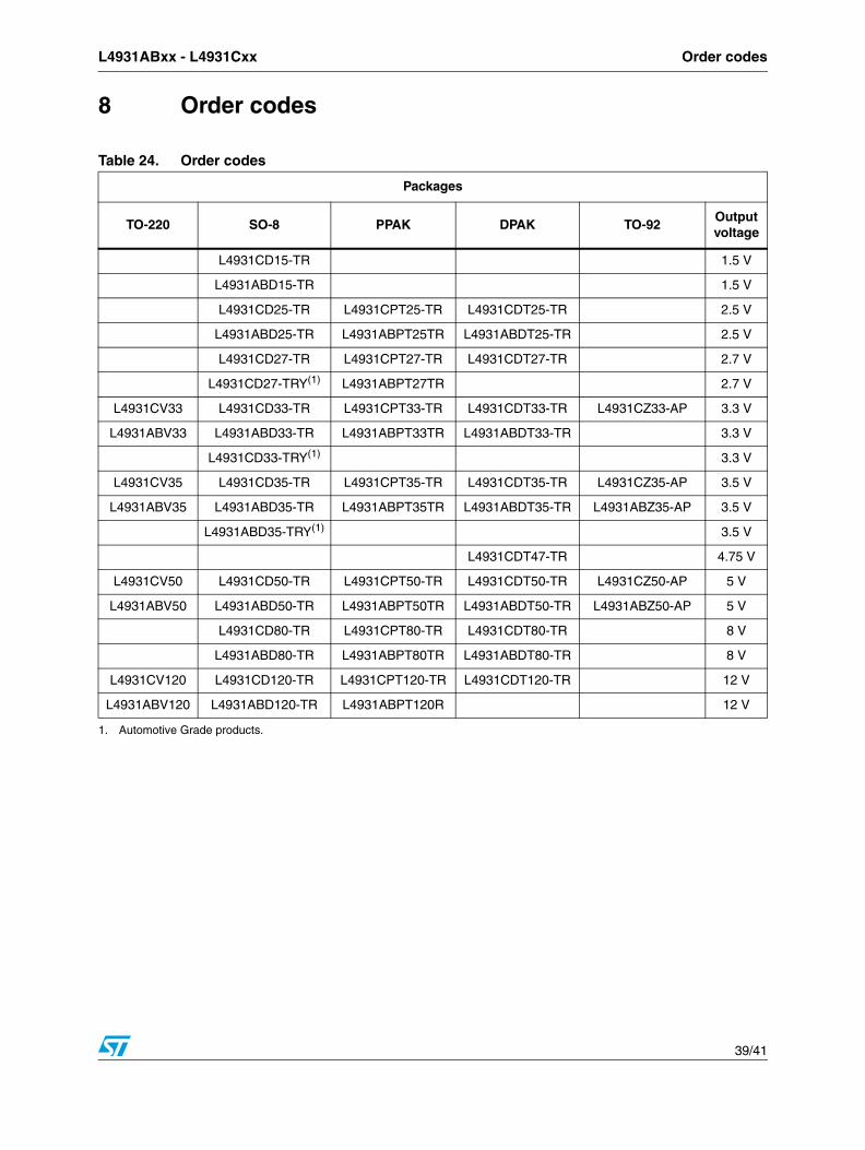
8 Order codes
Table 24. Order codes
Packages
TO-220 SO-8 PPAK DPAK TO-92Output voltage
L4931CD15-TR 1.5 V
L4931ABD15-TR 1.5 V
L4931CD25-TR L4931CPT25-TR L4931CDT25-TR 2.5 V
L4931ABD25-TR L4931ABPT25TR L4931ABDT25-TR 2.5 V
L4931CD27-TR L4931CPT27-TR L4931CDT27-TR 2.7 V
L4931CD27-TRY(1)
1. Automotive Grade products.
L4931ABPT27TR 2.7 V
L4931CV33 L4931CD33-TR L4931CPT33-TR L4931CDT33-TR L4931CZ33-AP 3.3 V
L4931ABV33 L4931ABD33-TR L4931ABPT33TR L4931ABDT33-TR 3.3 V
L4931CD33-TRY(1) 3.3 V
L4931CV35 L4931CD35-TR L4931CPT35-TR L4931CDT35-TR L4931CZ35-AP 3.5 V
L4931ABV35 L4931ABD35-TR L4931ABPT35TR L4931ABDT35-TR L4931ABZ35-AP 3.5 V
L4931ABD35-TRY(1) 3.5 V
L4931CDT47-TR 4.75 V
L4931CV50 L4931CD50-TR L4931CPT50-TR L4931CDT50-TR L4931CZ50-AP 5 V
L4931ABV50 L4931ABD50-TR L4931ABPT50TR L4931ABDT50-TR L4931ABZ50-AP 5 V
L4931CD80-TR L4931CPT80-TR L4931CDT80-TR 8 V
L4931ABD80-TR L4931ABPT80TR L4931ABDT80-TR 8 V
L4931CV120 L4931CD120-TR L4931CPT120-TR L4931CDT120-TR 12 V
L4931ABV120 L4931ABD120-TR L4931ABPT120R 12 V

Revision history L4931ABxx - L4931Cxx
40/41
9 Revision history
Table 25. Document revision history
Date Revision Changes
21-Jun-2004 11 Document updating.
14-Jun-2006 12 Order codes updated.
31-Jan-2008 13 Added: Table 1 and new order codes for Automotive grade products.
L4931ABxx - L4931Cxx
41/41
Please Read Carefully:
Information in this document is provided solely in connection with ST products. STMicroelectronics NV and its subsidiaries (“ST”) reserve theright to make changes, corrections, modifications or improvements, to this document, and the products and services described herein at anytime, without notice.
All ST products are sold pursuant to ST’s terms and conditions of sale.
Purchasers are solely responsible for the choice, selection and use of the ST products and services described herein, and ST assumes noliability whatsoever relating to the choice, selection or use of the ST products and services described herein.
No license, express or implied, by estoppel or otherwise, to any intellectual property rights is granted under this document. If any part of thisdocument refers to any third party products or services it shall not be deemed a license grant by ST for the use of such third party productsor services, or any intellectual property contained therein or considered as a warranty covering the use in any manner whatsoever of suchthird party products or services or any intellectual property contained therein.
UNLESS OTHERWISE SET FORTH IN ST’S TERMS AND CONDITIONS OF SALE ST DISCLAIMS ANY EXPRESS OR IMPLIEDWARRANTY WITH RESPECT TO THE USE AND/OR SALE OF ST PRODUCTS INCLUDING WITHOUT LIMITATION IMPLIEDWARRANTIES OF MERCHANTABILITY, FITNESS FOR A PARTICULAR PURPOSE (AND THEIR EQUIVALENTS UNDER THE LAWSOF ANY JURISDICTION), OR INFRINGEMENT OF ANY PATENT, COPYRIGHT OR OTHER INTELLECTUAL PROPERTY RIGHT.
UNLESS EXPRESSLY APPROVED IN WRITING BY AN AUTHORIZED ST REPRESENTATIVE, ST PRODUCTS ARE NOTRECOMMENDED, AUTHORIZED OR WARRANTED FOR USE IN MILITARY, AIR CRAFT, SPACE, LIFE SAVING, OR LIFE SUSTAININGAPPLICATIONS, NOR IN PRODUCTS OR SYSTEMS WHERE FAILURE OR MALFUNCTION MAY RESULT IN PERSONAL INJURY,DEATH, OR SEVERE PROPERTY OR ENVIRONMENTAL DAMAGE. ST PRODUCTS WHICH ARE NOT SPECIFIED AS "AUTOMOTIVEGRADE" MAY ONLY BE USED IN AUTOMOTIVE APPLICATIONS AT USER’S OWN RISK.
Resale of ST products with provisions different from the statements and/or technical features set forth in this document shall immediately voidany warranty granted by ST for the ST product or service described herein and shall not create or extend in any manner whatsoever, anyliability of ST.
ST and the ST logo are trademarks or registered trademarks of ST in various countries.
Information in this document supersedes and replaces all information previously supplied.
The ST logo is a registered trademark of STMicroelectronics. All other names are the property of their respective owners.
© 2008 STMicroelectronics - All rights reserved
STMicroelectronics group of companies
Australia - Belgium - Brazil - Canada - China - Czech Republic - Finland - France - Germany - Hong Kong - India - Israel - Italy - Japan - Malaysia - Malta - Morocco - Singapore - Spain - Sweden - Switzerland - United Kingdom - United States of America
www.st.com