Embed Size (px)
Citation preview
© Semiconductor Components Industries, LLC, 2013
December, 2013 − Rev. 61 Publication Order Number:
AN920/D
AN920/D
Theory and Applications of the MC34063 and�A78S40 SwitchingRegulator Control Circuits
This paper describes in detail the principle of operation of the MC34063 and μA78S40 switching regulator subsystems. Severalconverter design examples and numerous applications circuits with test data are included.
INTRODUCTIONThe MC34063 and μA78S40 are monolithic switching
regulator subsystems intended for use as dc to dc converters.These devices represent a significant advancement in theease of implementing highly efficient and yet simpleswitching power supplies. The use of switching regulatorsis becoming more pronounced over that of linear regulatorsbecause the size reductions in new equipment designsrequire greater conversion efficiency. Another majoradvantage of the switching regulator is that it has increasedapplication flexibility of output voltage. The output can beless than, greater than, or of opposite polarity to that of theinput voltage.
PRINCIPLE OF OPERATIONIn order to understand the difference in operation between
linear and switching regulators we must compare the blockdiagrams of the two step−down regulators shown in Figure1. The linear regulator consists of a stable reference, a highgain error amplifier, and a variable resistance series−passelement. The error amplifier monitors the output voltagelevel, compares it to the reference and generates a linearcontrol signal that varies between two extremes, saturationand cutoff. This signal is used to vary the resistance of theseries−pass element in a corrective fashion in order tomaintain a constant output voltage under varying inputvoltage and output load conditions.
The switching regulator consists of a stable reference anda high gain error amplifier identical to that of the linearregulator. This system differs in that a free running oscillatorand a gated latch have been added. The error amplifier againmonitors the output voltage, compares it to the referencelevel and generates a control signal. If the output voltage isbelow nominal, the control signal will go to a high state andturn on the gate, thus allowing the oscillator clock pulses todrive the series−pass element alternately from cutoff tosaturation. This will continue until the output voltage ispumped up slightly above its nominal value. At this time, the
control signal will go low and turn off the gate, terminatingany further switching of the series−pass element. The outputvoltage will eventually decrease to below nominal due to thepresence of an external load, and will initiate the switchingprocess again. The increase in conversion efficiency isprimarily due to the operation of the series−pass elementonly in the saturated or cutoff state. The voltage drop acrossthe element, when saturated, is small as is the dissipation.When in cutoff, the current through the element and likewisethe power dissipation are also small. There are othervariations of switching control. The most common are thefixed frequency pulse width modulator and the fixedon−time variable off−time types, where the on−offswitching is uninterrupted and regulation is achieved byduty cycle control. Generally speaking, the example givenin Figure 1b does apply to MC34063 and μA78S40.
Figure 1. Step−Down Regulators
+
−
Vin Vout
RefVoltage
ErrorAmp
Linear ControlSignal
+
−
Vin Vout
RefVoltage
ErrorAmp
DigitalControl Signal
GatedLatch
OSC
a. Linear Regulator
b. Switching Regulator
APPLICATION NOTE
http://onsemi.com
AN920/D
http://onsemi.com2
GENERAL DESCRIPTIONThe MC34063 series is a monolithic control circuit
containing all the active functions required for dc to dcconverters. This device contains an internal temperaturecompensated reference, comparator, controlled duty cycleoscillator with an active peak current limit circuit, driver,and a high current output switch. This series was specificallydesigned to be incorporated in step−up, step−down andvoltage−inverting converter applications. These functionsare contained in an 8−pin dual in−line package shown inFigure 2a.
The μA78S40 is identical to the MC34063 with theaddition of an on−board power catch diode, and anuncommitted operational amplifier. This device is in a16−pin dual in−line package which allows the reference andthe noninverting input of the comparator to be pinned out.These additional features greatly enhance the flexibility ofthis part and allow the implementation of more sophisticatedapplications. These may include series−pass regulation ofthe main output or of a derived second output voltage, atracking regulator configuration or even a second switchingregulator.
FUNCTIONAL DESCRIPTIONThe oscillator is composed of a current source and sink
which charges and discharges the external timing capacitorCT between an upper and lower preset threshold. The typicalcharge and discharge currents are 35 μA and 200 μArespectively, yielding about a one to six ratio. Thus theramp−up period is six times longer than that of theramp−down as shown in Figure 3. The upper threshold isequal to the internal reference voltage of 1.25 V and thelower is approximately equal to 0.75 V. The oscillator runscontinuously at a rate controlled by the selected value of CT.
During the ramp−up portion of the cycle, a Logic “1” ispresent at the “A” input of the AND gate. If the outputvoltage of the switching regulator is below nominal, a Logic“1” will also be present at the “B” input. This condition willset the latch and cause the “Q” output to go to a Logic “1”,enabling the driver and output switch to conduct. When theoscillator reaches its upper threshold, CT will start todischarge and Logic “0” will be present at the “A” input ofthe AND gate. This logic level is also connected to aninverter whose output presents a Logic “1” to the reset inputof the latch. This condition will cause “Q” to go low,disabling the driver and output switch. A logic truth table ofthese functional blocks is shown in Figure 4.
The output of the comparator can set the latch only duringthe ramp−up of CT and can initiate a partial or full on−cycleof output switch conduction. Once the comparator has setthe latch, it cannot reset it. The latch will remain set until CTbegins ramping down. Thus the comparator can initiateoutput switch conduction, but cannot terminate it and thelatch is always reset when CT begins ramping down. Thecomparator’s output will be at a Logic “0” when the outputvoltage of the switching regulator is above nominal. Under
these conditions, the comparator’s output can inhibit aportion of the output switch on−cycle, a complete cycle, acomplete cycle plus a portion of one cycle, multiple cycles,or multiple cycles plus a portion of one cycle.
Figure 2. Functional Block Diagrams
8
7
6
5
1
2
3
4
Q1
Q2S
R
Q
LatchB
A
SwitchCollector
SwitchEmitter
TimingCapacitor
Ground
DriveCollector
IpkSense
VCC
ComparatorInverting
Input
Ipk CTOSC
+
−
1.25 VReferenceRegulator
a. MC34063
b. �A78S40
9
8
10
7
11
6
12
5
13
4
14
3
15
2
16
1
Sw
itch
Col
lect
or
Driv
erC
olle
ctor
I pk
Sen
se
VC
C
Tim
ing
Cap
acito
r
GN
D
Inve
rtin
gIn
put
Non
inve
rtin
gIn
put
Dio
deC
atho
de
Dio
deA
node
VC
CO
p A
mp
Inve
rtin
gIn
put
Ref
Out
put
Non
inve
rtin
gIn
put
Out
put
Sw
itch
Em
itter
1.25 VRef
CT IpkOSC
+
−
D1
170
A
B
+
−
S
R
Q
Latch
OpAmp
Comp
GND
Comp
170
Figure 3. CT Voltage Waveform
V
t
Upper Threshold 1.25 V Typical
Lower Threshold 0.75 V Typical
t
Discharge
6t Charge
AN920/D
http://onsemi.com3
Active Condition ofTiming Capacitor, CT
AND Gate Inputs Latch InputsOutputSwitch Comments on State of Output SwitchA B S R
Begins Ramp−Up 0 0 0 Switching regulator’s output is ≥ nominal (‘B’ = 0).
Begins Ramp−Down 0 0 0 No change since ‘B’ was 0 before CT Ramp−Down.
Ramping Down 0 0 1 0 No change even though switching regulator’soutput < nominal. Output switch cannot beinitiated during RT Ramp−Down.
Ramping Down 0 0 1 0 No change since output switch conductionwas terminated when ‘A’ went to 0.
Ramping Up 1 0 Switching regulator’s output went < nominalduring CT Ramp−Up (‘B’ → 1). Partial on−cycle for output switch.
Ramping Up 1 0 1 Switching regulator’s output went ≥ nominal(‘B’ → 0) during CT Ramp−Up. No changesince ‘B’ cannot reset latch.
Begins Ramp−Up 1 Complete on−cycle since ‘B’ was 1 before CTstarted Ramp−Up.
Begins Ramp−Down 1 Output switch conduction is always termi-nated whenever CT is Ramping Down.
Figure 4. Logic Truth Table of Functional Blocks
Current limiting is accomplished by monitoring thevoltage drop across an external sense resistor placed in serieswith VCC and the output switch. The voltage drop developedacross this resistor is monitored by the Ipk Sense pin. Whenthis voltage becomes greater than 330 mV, the current limitcircuitry provides an additional current path to charge thetiming capacitor CT. This causes it to rapidly reach the upperoscillator threshold, thereby shortening the time of outputswitch conduction and thus reducing the amount of energystored in the inductor. This can be observed as an increasein the slope of the charging portion of the CT voltage
waveform as shown in Figure 5. Operation of the switchingregulator in an overload or shorted condition will cause avery short but finite time of output conduction followed byeither a normal or extended off−time internal provided bythe oscillator ramp−down time of CT. The extended intervalis the result of charging CT beyond the upper oscillatorthreshold by overdriving the current limit sense input. Thiscan be caused by operating the switching regulator with aseverely overloaded or shorted output or having the inputvoltage grossly above the nominal design value.
Quiescent OperationStartup
Figure 5. Typical Operating Waveforms
Comparator Output
Timing Capacitor, CT
Output Switch
Nominal Output VoltageLevel
Output Voltage
On
Off
1
0
AN920/D
http://onsemi.com4
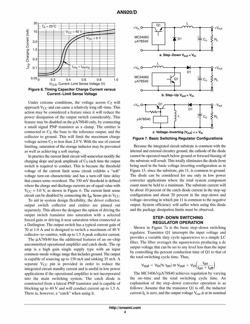
Figure 6. Timing Capacitor Charge Current versusCurrent−Limit Sense Voltage
0
I chg
, Cha
rgin
g C
urre
nt (
mA
)
VCLS, Current−Limit Sense Voltage (V)0.2 0.4 0.6 0.8 1.00.03
0.1
0.3
1.0
3.0
10
30TA = 25°C
VCC = 40 V
VCC = 5 V
Ichg = Idischg
Under extreme conditions, the voltage across CT willapproach VCC and can cause a relatively long off−time. Thisaction may be considered a feature since it will reduce thepower dissipation of the output switch considerably. Thisfeature may be disabled on the μA78S40 only, by connectinga small signal PNP transistor as a clamp. The emitter isconnected to CT, the base to the reference output, and thecollector to ground. This will limit the maximum chargevoltage across CT to less than 2.0 V. With the use of currentlimiting, saturation of the storage inductor may be preventedas well as achieving a soft startup.
In practice the current limit circuit will somewhat modify thecharging slope and peak amplitude of CT each time the outputswitch is required to conduct. This is because the thresholdvoltage of the current limit sense circuit exhibits a “soft”voltage turn−on characteristic and has a turn−off time delaythat causes some overshoot. The 330 mV threshold is definedwhere the charge and discharge currents are of equal value withVCC = 5.0 V, as shown in Figure 6. The current limit sensecircuit can be disabled by connecting the Ipk Sense pin to VCC.
To aid in system design flexibility, the driver collector,output switch collector and emitter are pinned outseparately. This allows the designer the option of driving theoutput switch transistor into saturation with a selectedforced gain or driving it near saturation when connected asa Darlington. The output switch has a typical current gain of70 at 1.0 A and is designed to switch a maximum of 40 Vcollector−to−emitter, with up to 1.5 A peak collector current.
The μA78S40 has the additional features of an on−chipuncommitted operational amplifier and catch diode. The opamp is a high gain single supply type with an inputcommon−mode voltage range that includes ground. The outputis capable of sourcing up to 150 mA and sinking 35 mA. Aseparate VCC pin is provided in order to reduce theintegrated circuit standby current and is useful in low powerapplications if the operational amplifier is not incorporatedinto the main switching system. The catch diode isconstructed from a lateral PNP transistor and is capable ofblocking up to 40 V and will conduct current up to 1.5 A.There is, however, a “catch” when using it.
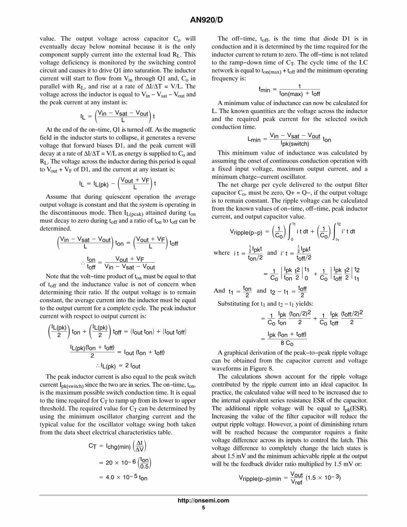
Figure 7. Basic Switching Regulator Configurations
+Vin +Vout
RL
+Co
L
D1
Q1
MC34063μA78S40
+Vin +Vout
RL
+Co
L
D1
Q1MC34063μA78S40
+Vin −Vout
RL+ CoL
D1
Q1
μA78S40
a. Step−Down Vout � Vin
b. Step−Up Vout � Vin
c. Voltage−Inverting |Vout| � � Vin
Because the integrated circuit substrate is common with theinternal and external circuitry ground, the cathode of the diodecannot be operated much below ground or forward biasing ofthe substrate will result. This totally eliminates the diode frombeing used in the basic voltage inverting configuration as inFigure 15, since the substrate, pin 11, is common to ground.The diode can be considered for use only in low powerconverter applications where the total system componentcount must be held to a minimum. The substrate current willbe about 10 percent of the catch diode current in the step−upconfiguration and about 20 percent in the step−down andvoltage−inverting in which pin 11 is common to the negativeoutput. System efficiency will suffer when using this diodeand the package dissipation limits must be observed.
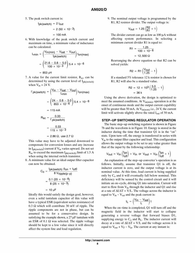
STEP−DOWN SWITCHINGREGULATOR OPERATION
Shown in Figure 7a is the basic step−down switchingregulator. Transistor Q1 interrupts the input voltage andprovides a variable duty cycle squarewave to a simple LCfilter. The filter averages the squarewaves producing a dcoutput voltage that can be set to any level less than the inputby controlling the percent conduction time of Q1 to that ofthe total switching cycle time. Thus,
Vout � Vin�% ton� or Vout � Vin� tonton � toff
�The MC34063/μA78S40 achieves regulation by varying
the on−time and the total switching cycle time. Anexplanation of the step−down converter operation is asfollows: Assume that the transistor Q1 is off, the inductorcurrent IL is zero, and the output voltage Vout is at its nominal
AN920/D
http://onsemi.com5
value. The output voltage across capacitor Co willeventually decay below nominal because it is the onlycomponent supply current into the external load RL. Thisvoltage deficiency is monitored by the switching controlcircuit and causes it to drive Q1 into saturation. The inductorcurrent will start to flow from Vin through Q1 and, Co inparallel with RL, and rise at a rate of ΔI/ΔT = V/L. Thevoltage across the inductor is equal to Vin − Vsat − Vout andthe peak current at any instant is:
IL � �Vin � Vsat � VoutL
� t
At the end of the on−time, Q1 is turned off. As the magneticfield in the inductor starts to collapse, it generates a reversevoltage that forward biases D1, and the peak current willdecay at a rate of ΔI/ΔT = V/L as energy is supplied to Co andRL. The voltage across the inductor during this period is equalto Vout + VF of D1, and the current at any instant is:
IL � IL(pk) ��Vout � VFL
� t
Assume that during quiescent operation the averageoutput voltage is constant and that the system is operating inthe discontinuous mode. Then IL(peak) attained during tonmust decay to zero during toff and a ratio of ton to toff can bedetermined.
�Vin � Vsat � VoutL
� ton � �Vout � VFL
� toff
� tontoff
� Vout � VFVin � Vsat � Vout
Note that the volt−time product of ton must be equal to thatof toff and the inductance value is not of concern whendetermining their ratio. If the output voltage is to remainconstant, the average current into the inductor must be equalto the output current for a complete cycle. The peak inductorcurrent with respect to output current is:
�IL(pk)2� ton ��IL(pk)
2� toff � �Iout ton� � �Iout toff�
�IL(pk) � 2 Iout
IL(pk)(ton � toff)2
� Iout (ton � toff)
The peak inductor current is also equal to the peak switchcurrent Ipk(switch) since the two are in series. The on−time, ton,is the maximum possible switch conduction time. It is equalto the time required for CT to ramp up from its lower to upperthreshold. The required value for CT can be determined byusing the minimum oscillator charging current and thetypical value for the oscillator voltage swing both takenfrom the data sheet electrical characteristics table.
CT � Ichg(min) ��t�V�
� 20 � 10− 6 �ton0.5�
� 4.0 � 10− 5 ton
The off−time, toff, is the time that diode D1 is inconduction and it is determined by the time required for theinductor current to return to zero. The off−time is not relatedto the ramp−down time of CT. The cycle time of the LCnetwork is equal to ton(max) + toff and the minimum operatingfrequency is:
fmin � 1ton(max) � toff
A minimum value of inductance can now be calculated forL. The known quantities are the voltage across the inductorand the required peak current for the selected switchconduction time.
Lmin � Vin � Vsat � VoutIpk(switch)
ton
This minimum value of inductance was calculated byassuming the onset of continuous conduction operation witha fixed input voltage, maximum output current, and aminimum charge−current oscillator.
The net charge per cycle delivered to the output filtercapacitor Co, must be zero, Q+ = Q−, if the output voltageis to remain constant. The ripple voltage can be calculatedfrom the known values of on−time, off−time, peak inductorcurrent, and output capacitor value.
Vripple(p−p) � � 1Co� t1
0
i t dt �� 1Co� t2
t1
i t dt
i t �12 Ipkt
ton�2where and i t �
12 Ipkt
toff�2
� 1Co� Ipkton
t22� t10
� 1Co� Ipktoff
t22� t2
t1
t1 � ton2
And and t2 � t1 � toff2
Substituting for t1 and t2 − t1 yields:
�Ipk (ton � toff)
8 Co
� 1Co
Ipkton
(ton�2)2
2� 1
Co
Ipktoff
(toff�2)2
2
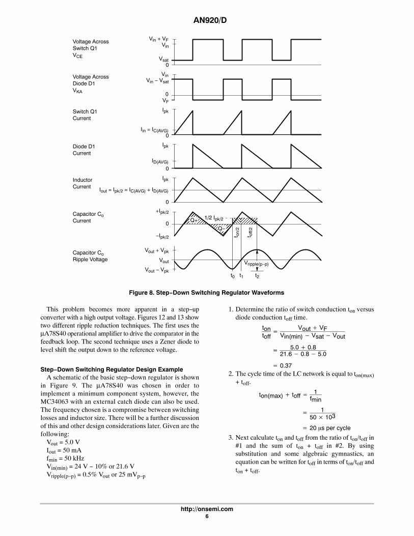
A graphical derivation of the peak−to−peak ripple voltagecan be obtained from the capacitor current and voltagewaveforms in Figure 8.
The calculations shown account for the ripple voltagecontributed by the ripple current into an ideal capacitor. Inpractice, the calculated value will need to be increased due tothe internal equivalent series resistance ESR of the capacitor.The additional ripple voltage will be equal to Ipk(ESR).Increasing the value of the filter capacitor will reduce theoutput ripple voltage. However, a point of diminishing returnwill be reached because the comparator requires a finitevoltage difference across its inputs to control the latch. Thisvoltage difference to completely change the latch states isabout 1.5 mV and the minimum achievable ripple at the outputwill be the feedback divider ratio multiplied by 1.5 mV or:
Vripple(p−p)min � VoutVref
(1.5 � 10− 3)
AN920/D
http://onsemi.com6
ÏÏÏÏÌÌÌÌ
Figure 8. Step−Down Switching Regulator Waveforms
ÌÌÌÌÌÌÌÌÌÌÌ
ÌÌÌ
Voltage AcrossSwitch Q1VCE
Voltage AcrossDiode D1VKA
Switch Q1Current
Diode D1Current
InductorCurrent
Capacitor CoCurrent
Capacitor CoRipple Voltage
Vin + VFVin
Vsat0
VinVin − Vsat
0VF
Ipk
Iin = IC(AVG)0
Ipk
ID(AVG)
0
+Ipk/2
0
−Ipk/2
Ipk
Iout = Ipk/2 = IC(AVG) + ID(AVG)
0
Vout + Vpk
Vout
Vout − Vpk
Q−
Q+ 1/2 Ipk/2
t0 t1 t2
Vripple(p−p)
t on/
2
t off/
2
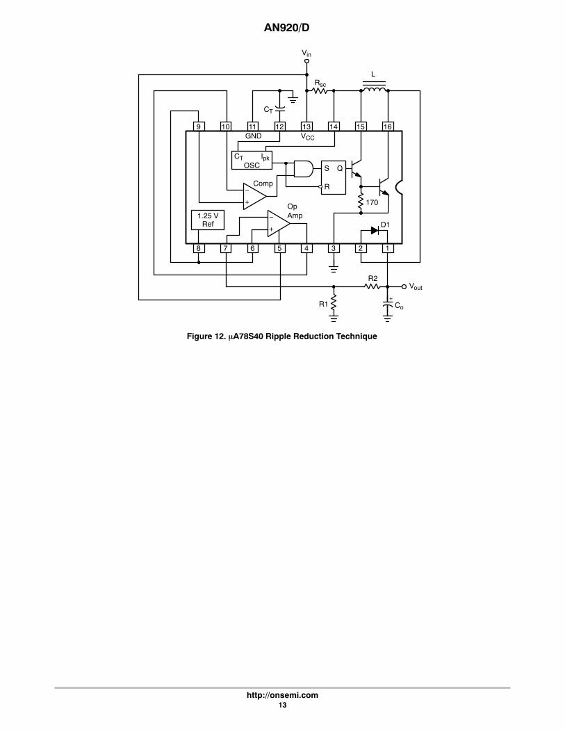
This problem becomes more apparent in a step−upconverter with a high output voltage. Figures 12 and 13 showtwo different ripple reduction techniques. The first uses theμA78S40 operational amplifier to drive the comparator in thefeedback loop. The second technique uses a Zener diode tolevel shift the output down to the reference voltage.
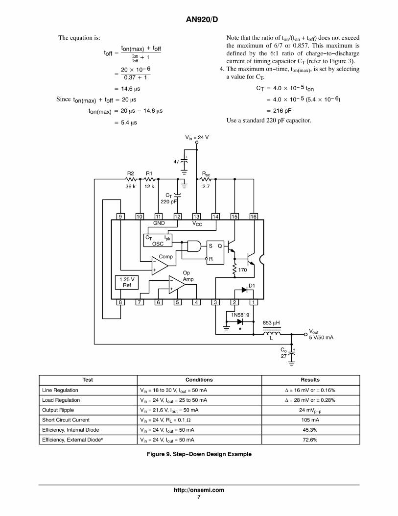
Step−Down Switching Regulator Design ExampleA schematic of the basic step−down regulator is shown
in Figure 9. The μA78S40 was chosen in order toimplement a minimum component system, however, theMC34063 with an external catch diode can also be used.The frequency chosen is a compromise between switchinglosses and inductor size. There will be a further discussionof this and other design considerations later. Given are thefollowing:
Vout = 5.0 VIout = 50 mAfmin = 50 kHzVin(min) = 24 V − 10% or 21.6 VVripple(p−p) = 0.5% Vout or 25 mVp−p
1. Determine the ratio of switch conduction ton versusdiode conduction toff time.
� 0.37
tontoff
� Vout � VFVin(min) � Vsat � Vout
� 5.0 � 0.821.6 � 0.8 � 5.0
2. The cycle time of the LC network is equal to ton(max)+ toff.
� 20 �s per cycle
ton(max) � toff �1
fmin
� 150 � 103
3. Next calculate ton and toff from the ratio of ton/toff in#1 and the sum of ton + toff in #2. By usingsubstitution and some algebraic gymnastics, anequation can be written for toff in terms of ton/toff andton + toff.
AN920/D
http://onsemi.com7
The equation is:
� 14.6 �s
toff �ton(max) � toff
tontoff
� 1
�20 � 10− 6
0.37 � 1
ton(max) � toff � 20 �s
ton(max) � 20 �s � 14.6 �s
� 5.4 �s
Since
Note that the ratio of ton/(ton + toff) does not exceedthe maximum of 6/7 or 0.857. This maximum isdefined by the 6:1 ratio of charge−to−dischargecurrent of timing capacitor CT (refer to Figure 3).
4. The maximum on−time, ton(max), is set by selectinga value for CT.
CT � 4.0 � 10− 5 ton
� 4.0 � 10− 5 (5.4 � 10− 6)
� 216 pF
Use a standard 220 pF capacitor.
9
8
10
7
11
6
12
5
13
4
14
3
15
2
16
1
1.25 VRef
CT IpkOSC
+
−
D1
170
+
−
S
R
Q
OpAmp
Comp
GND VCC
1N5819
+Co27
Vout5 V/50 mA
853 μH
L
+47
CT220 pF
Rsc
2.7
R1
12 k
R2
36 k
Vin = 24 V
*
Test Conditions Results
Line Regulation Vin = 18 to 30 V, Iout = 50 mA Δ = 16 mV or ± 0.16%
Load Regulation Vin = 24 V, Iout = 25 to 50 mA Δ = 28 mV or ± 0.28%
Output Ripple Vin = 21.6 V, Iout = 50 mA 24 mVp−p
Short Circuit Current Vin = 24 V, RL = 0.1 Ω 105 mA
Efficiency, Internal Diode Vin = 24 V, Iout = 50 mA 45.3%
Efficiency, External Diode* Vin = 24 V, Iout = 50 mA 72.6%
Figure 9. Step−Down Design Example
AN920/D
http://onsemi.com8
5. The peak switch current is:
Ipk(switch) � 2 Iout
� 2 (50 � 10− 3)
� 100 mA
6. With knowledge of the peak switch current andmaximum on time, a minimum value of inductancecan be calculated.
Lmin � �Vin(min) � Vsat � VoutIpk(switch)
� ton(max)
� �21.6 � 0.8 � 5.0100 � 10− 3
� 5.4 � 10− 6
� 853 �H
7. A value for the current limit resistor, Rsc, can bedetermined by using the current level of Ipk(switch)when Vin = 24 V.
Ipk(switch) � �Vin � Vsat � VoutLmin
� ton(max)
� �24 � 0.8 � 5.0853 � 10− 6
� 5.4 � 10− 6
� 115 mA
Rsc � 0.33Ipk(switch)
� 0.33115 � 10− 3
� 2.86 �, use 2.7 �
This value may have to be adjusted downward tocompensate for conversion losses and any increasein Ipk(switch) current if Vin varies upward. Do not setRsc to exceed the maximum Ipk(switch) limit of 1.5 Awhen using the internal switch transistor.
8. A minimum value for an ideal output filter capacitorcan now be obtained.
Co �Ipk(switch) (ton � toff)
8 Vripple(p−p)
�0.1 (20 � 10− 6)
8 (25 � 10− 3)
� 10 �F
Ideally this would satisfy the design goal, however,even a solid tantalum capacitor of this value willhave a typical ESR (equivalent series resistance) of0.3 Ω which will contribute 30 mV of ripple. Theripple components are not in phase, but can beassumed to be for a conservative design. Insatisfying the example shown, a 27 μF tantalum withan ESR of 0.1 Ω was selected. The ripple voltageshould be kept to a low value since it will directlyaffect the system line and load regulation.
9. The nominal output voltage is programmed by theR1, R2 resistor divider. The output voltage is:
Vout � 1.25 �R2R1
� 1�The divider current can go as low as 100 μA withoutaffecting system performance. In selecting aminimum current divider R1 is equal to:
R1 � 1.25100 � 10− 6
� 12, 500 �
Rearranging the above equation so that R2 can besolved yields:
R2 � R1 �Vout1.25
� 1�If a standard 5% tolerance 12 k resistor is chosen forR1, R2 will also be a standard value.
R2 � 12 � 103 � 5.01.25
� 1�� 36 k
Using the above derivation, the design is optimized tomeet the assumed conditions. At Vin(min), operation is at theonset of continuous mode and the output current capabilitywill be greater than 50 mA. At Vin(nom) i.e., 24 V, the currentlimit will activate slightly above the rated Iout of 50 mA.
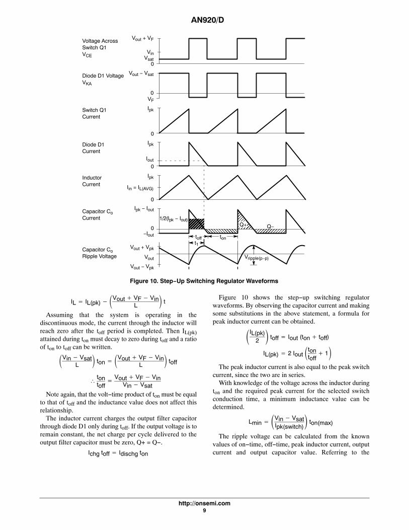
STEP−UP SWITCHING REGULATOR OPERATIONThe basic step−up switching regulator is shown in Figure
7b and the waveform is in Figure 10. Energy is stored in theinductor during the time that transistor Q1 is in the “on”state. Upon turn−off, the energy is transferred in series withVin to the output filter capacitor and load. This configurationallows the output voltage to be set to any value greater thanthat of the input by the following relationship:
Vout � Vin �tontoff� � Vin or Vout � Vin �ton
toff� 1�
An explanation of the step−up converter’s operation is asfollows. Initially, assume that transistor Q1 is off, theinductor current is zero, and the output voltage is at itsnominal value. At this time, load current is being suppliedonly by Co and it will eventually fall below nominal. Thisdeficiency will be sensed by the control circuit and it willinitiate an on−cycle, driving Q1 into saturation. Current willstart to flow from Vin through the inductor and Q1 and riseat a rate of ΔI/ΔT = V/L. The voltage across the inductor isequal to Vin − Vsat and the peak current is:
IL � �Vin � VsatL
� t
When the on−time is completed, Q1 will turn off and themagnetic field in the inductor will start to collapsegenerating a reverse voltage that forward biases D1,supplying energy to Co and RL. The inductor current willdecay at a rate of ΔI/ΔT = V/L and the voltage across it isequal to Vout + VF − Vin. The current at any instant is:
AN920/D
http://onsemi.com9
ÌÌÌÌ
Figure 10. Step−Up Switching Regulator Waveforms
ÌÌÌÌÌÌÏÏÏÏÏ
ÑÑÑÑ
Voltage AcrossSwitch Q1VCE
Diode D1 VoltageVKA
Switch Q1Current
Diode D1Current
InductorCurrent
Capacitor CoCurrent
Capacitor CoRipple Voltage
Vout + VF
VinVsat
0
Vout − Vsat
0VF
Ipk
0
Ipk
Iout
0
Ipk − Iout
0−Iout
Ipk
Iin = IL(AVG)
0
Vout + Vpk
Vout
Vout − Vpk
Q+
Vripple(p−p)
toff
1/2(Ipk − Iout)
tont1
Q−
IL � IL(pk) ��Vout � VF � VinL
� t
Assuming that the system is operating in thediscontinuous mode, the current through the inductor willreach zero after the toff period is completed. Then IL(pk)attained during ton must decay to zero during toff and a ratioof ton to toff can be written.
�Vin � VsatL
� ton � �Vout � VF � VinL
� toff
� tontoff
� Vout � VF � VinVin � Vsat
Note again, that the volt−time product of ton must be equalto that of toff and the inductance value does not affect thisrelationship.
The inductor current charges the output filter capacitorthrough diode D1 only during toff. If the output voltage is toremain constant, the net charge per cycle delivered to theoutput filter capacitor must be zero, Q+ = Q−.
Ichg toff � Idischg ton
Figure 10 shows the step−up switching regulatorwaveforms. By observing the capacitor current and makingsome substitutions in the above statement, a formula forpeak inductor current can be obtained.
�IL(pk)2� toff � Iout (ton � toff)
IL(pk) � 2 Iout �tontoff
� 1�The peak inductor current is also equal to the peak switch
current, since the two are in series.With knowledge of the voltage across the inductor during
ton and the required peak current for the selected switchconduction time, a minimum inductance value can bedetermined.
Lmin � �Vin � VsatIpk(switch)
� ton(max)
The ripple voltage can be calculated from the knownvalues of on−time, off−time, peak inductor current, outputcurrent and output capacitor value. Referring to the
AN920/D
http://onsemi.com10
capacitor current waveforms in Figure 10, t1 is defined as thecapacitor charging interval. Solving for t1 in known termsyields:
Ipk � Ioutt1
�Ipktoff
�t1 � �Ipk � IoutIpk
� toff
And the current during t1 can be written:
I � �Ipk � Ioutt1
� t
The ripple voltage is:
Vripple(p−p) � � 1Co� t1
0
Ipk � Ioutt1
t dt
� 1Co� Ipk � Iout
t1t22� t10
� 1Co
(Ipk � Iout)2
t1
Substituting for t1 yields:
� 1Co
(Ipk � Iout)2
(Ipk � Iout)
Ipktoff
�(Ipk � Iout)2 toff
2 Ipk Co
A simplified formula that will give an error of less than 5%for a voltage step−up greater than 3 with an ideal capacitoris shown:
Vripple(p−p) �IoutCo� ton
This neglects a small portion of the total Q− area. The areaneglected is equal to:
A � (toff � t1)Iout2
Step−Up Switching Regulator Design ExampleThe basic step−up regulator schematic is shown in Figure
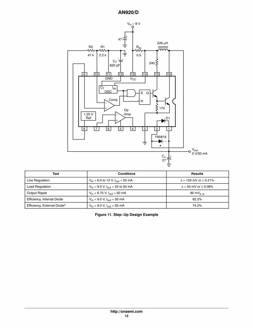
11. The μA78S40 again was chosen in order to implementa minimum component system. The following conditionsare given:
Vout = 28 VIout = 50 mAfmin = 50 kHzVin(min) = 9.0 V − 25% or 6.75 VVripple(p−p) = 0.5% Vout or 140 mVp−p
1. Determine the ratio of switch conduction ton versusdiode conduction toff time.
tontoff
�Vout � VF � Vin(min)
Vin(min) � Vsat
� 28 � 0.8 � 6.756.75 � 0.3
� 3.422. The cycle time of the LC network is equal to ton(max)
+ toff.
ton(max) � toff �1
fmin
� 150 � 103
� 20 �s per cycle
3. Next calculate ton and toff from the ratio of ton/toff in#1 and the sum of ton + toff in #2.
toff �20 � 10− 6
3.42 � 1
� 4.5 �s
ton � 20 �s � 4.5 �s
� 15.5 �s
Note that the ratio of ton/(ton + toff) does not exceedthe maximum of 0.857.
4. The maximum on−time, ton(max), is set by selectinga value for CT.
CT � 4.0 � 10− 5 ton
� 4.0 � 10− 5 (15.5 � 10− 6)
� 620 pF
5. The peak switch current is:
Ipk(switch) � 2 Iout �tontoff
� 1�� 2 (50 � 10− 3) (3.42 � 1)
� 442 mA
6. A minimum value of inductance can be calculatedsince the maximum on−time and peak switch currentare known.
Lmin � �Vin(min) � VsatIpk(switch)
� ton
� � 6.75 � 0.3442 � 10− 3
� 15.5 � 10− 6
� 226 �H
AN920/D
http://onsemi.com11
7. A value for the current limit resistor, Rsc, can now bedetermined by using the current level of Ipk(switch)when Vin = 9.0 V.
Ipk(switch) � �Vin � VsatLmin
� ton(max)
� � 9.0 � 0.3226 � 10− 6
� 15.5 � 10− 6
� 597 mA
Rsc � 0.33Ipk(switch)
� 0.33597 � 10− 3
� 0.55 �, use 0.5 �
Note that current limiting in this basic step−upconfiguration will only protect the switch transistorfrom overcurrent due to inductor saturation. If theoutput is severely overloaded or shorted, D1, L, orRsc may be destroyed since they form a direct pathfrom Vin to Vout. Protection may be achieved bycurrent limiting Vin or replacing the inductor with1:1 turns ratio transformer.
8. An approximate value for an ideal output filtercapacitor is:
Co 9 � IoutVripple(p−p)
ton
9 � 50 � 10− 3
140 � 10− 315.5 � 10− 6
50 �F
The ripple contribution due to the gain of thecomparator:
Vripple(p−p) �VoutVref
1.5 � 10− 3
� 281.25
1.5 � 10− 3
� 33.6 mV
A 27 μF tantalum capacitor with an ESR of 0.10 Ωwas again chosen. The ripple voltage due to thecapacitance value is 28.7 mV and 44.2 mV due toESR. This yields a total ripple voltage of:
Eripple(p−p) �VoutVref
1.5 � 10− 3 � IoutCo
ton � Ipk ESR
� 33.6 mV � 28.7 mV � 44.2 mV
� 107 mV
AN920/D
http://onsemi.com12
9
8
10
7
11
6
12
5
13
4
14
3
15
2
16
1
1.25 VRef
CT IpkOSC
+
−
D1
170
+
−
S
R
Q
OpAmp
Comp
GND VCC
1N5819
+Co27
Vout5 V/50 mA
226 μH
+47
CT620 pF
Rsc
0.5
R1
2.2 k
R2
47 k
Vin = 9 V
240
*
Test Conditions Results
Line Regulation Vin = 6.0 to 12 V, Iout = 50 mA Δ = 120 mV or ± 0.21%
Load Regulation Vin = 9.0 V, Iout = 25 to 50 mA Δ = 50 mV or ± 0.09%
Output Ripple Vin = 6.75 V, Iout = 50 mA 90 mVp−p
Efficiency, Internal Diode Vin = 9.0 V, Iout = 50 mA 62.2%
Efficiency, External Diode* Vin = 9.0 V, Iout = 50 mA 74.2%
Figure 11. Step−Up Design Example
AN920/D
http://onsemi.com13
Figure 12. �A78S40 Ripple Reduction Technique
9
8
10
7
11
6
12
5
13
4
14
3
15
2
16
1
1.25 VRef
CT IpkOSC
+
−
D1
170
+
−
S
R
Q
OpAmp
Comp
GND VCC
+Co
Vout
L
CT
Rsc
Vin
R2
R1
AN920/D
http://onsemi.com14
8
7
6
5
1
2
3
4
Q1
Q2S
R
Q
Ipk CTOSC
+
−
1.25 VReferenceRegulator
Comp
VCC
Rsc
Vin
L
CT
R1
D1
Co+
Vout
VZ = Vout − 1.25 V
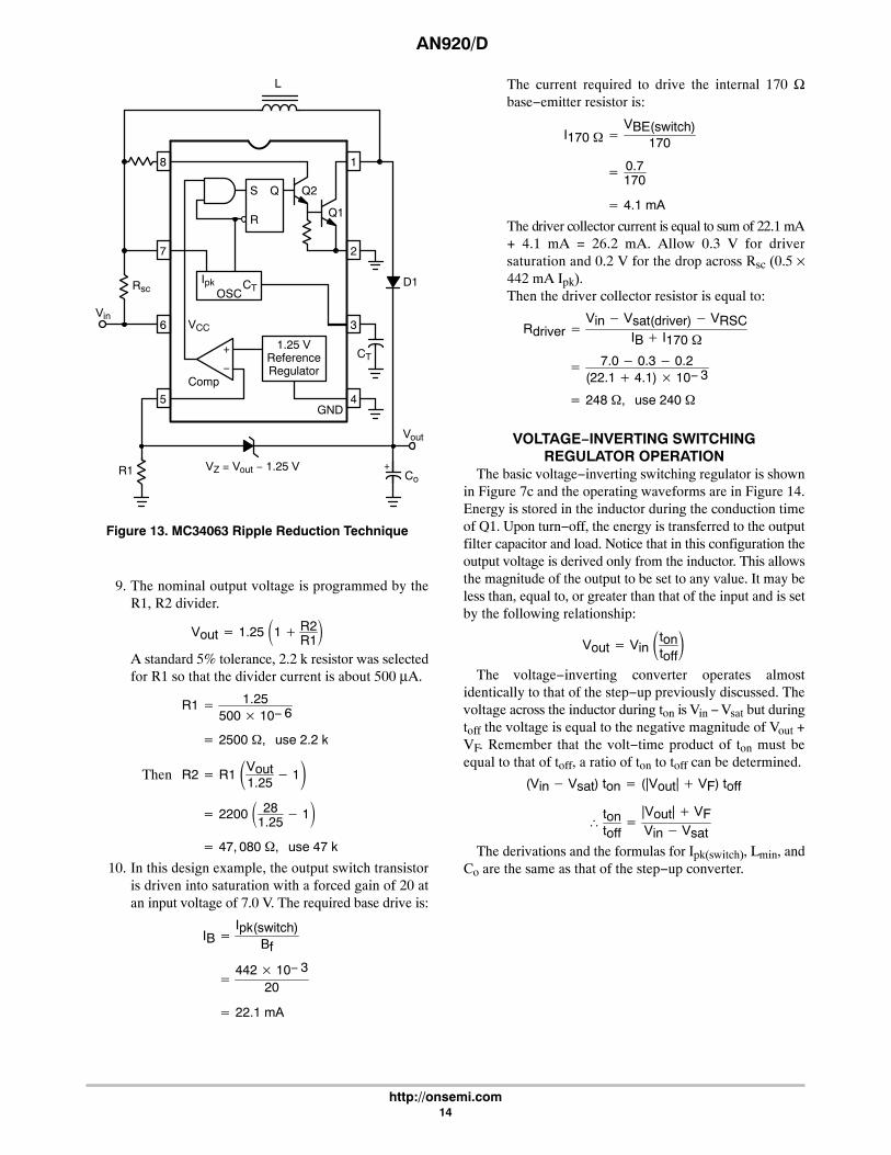
Figure 13. MC34063 Ripple Reduction Technique
GND
9. The nominal output voltage is programmed by theR1, R2 divider.
Vout � 1.25 �1 � R2R1�
A standard 5% tolerance, 2.2 k resistor was selectedfor R1 so that the divider current is about 500 μA.
R1 � 1.25500 � 10− 6
� 2500 �, use 2.2 k
R2 � R1 �Vout1.25
� 1�Then
� 2200 � 281.25
� 1�� 47, 080 �, use 47 k
10. In this design example, the output switch transistoris driven into saturation with a forced gain of 20 atan input voltage of 7.0 V. The required base drive is:
IB �Ipk(switch)
Bf
�442 � 10− 3
20
� 22.1 mA
The current required to drive the internal 170 Ωbase−emitter resistor is:
I170 � �VBE(switch)
170
� 0.7170
� 4.1 mA
The driver collector current is equal to sum of 22.1 mA+ 4.1 mA = 26.2 mA. Allow 0.3 V for driversaturation and 0.2 V for the drop across Rsc (0.5 ×442 mA Ipk).Then the driver collector resistor is equal to:
Rdriver �Vin � Vsat(driver) � VRSC
IB � I170 �
� 7.0 � 0.3 � 0.2(22.1 � 4.1) � 10− 3
� 248 �, use 240 �
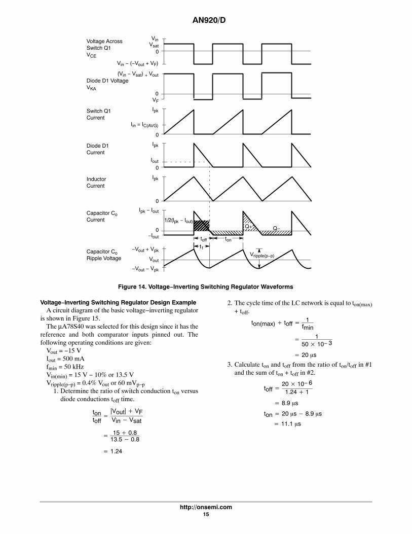
VOLTAGE−INVERTING SWITCHINGREGULATOR OPERATION
The basic voltage−inverting switching regulator is shownin Figure 7c and the operating waveforms are in Figure 14.Energy is stored in the inductor during the conduction timeof Q1. Upon turn−off, the energy is transferred to the outputfilter capacitor and load. Notice that in this configuration theoutput voltage is derived only from the inductor. This allowsthe magnitude of the output to be set to any value. It may beless than, equal to, or greater than that of the input and is setby the following relationship:
Vout � Vin �tontoff�
The voltage−inverting converter operates almostidentically to that of the step−up previously discussed. Thevoltage across the inductor during ton is Vin − Vsat but duringtoff the voltage is equal to the negative magnitude of Vout +VF. Remember that the volt−time product of ton must beequal to that of toff, a ratio of ton to toff can be determined.
�tontoff
�|Vout| � VFVin � Vsat
(Vin � Vsat) ton � (|Vout| � VF) toff
The derivations and the formulas for Ipk(switch), Lmin, andCo are the same as that of the step−up converter.
AN920/D
http://onsemi.com15
ÌÌÌÌ
Figure 14. Voltage−Inverting Switching Regulator Waveforms
ÌÌÌÌÌÌÌÌÌÏÏÏÏ
ÑÑÑÑÑÑ
Voltage AcrossSwitch Q1VCE
Diode D1 VoltageVKA
Switch Q1Current
Diode D1Current
InductorCurrent
Capacitor CoCurrent
Capacitor CoRipple Voltage
VinVsat
Vin − (−Vout + VF)
0
(Vin − Vsat) + Vout
0VF
Ipk
0
Ipk
Iout
0
Ipk − Iout
0−Iout
Ipk
0
−Vout + Vpk
Vout
−Vout − Vpk
Q+
Vripple(p−p)
toff
1/2(Ipk − Iout)
ton
t1
Iin = IC(AVG)
Q−
Voltage−Inverting Switching Regulator Design ExampleA circuit diagram of the basic voltage−inverting regulator
is shown in Figure 15.The μA78S40 was selected for this design since it has the
reference and both comparator inputs pinned out. Thefollowing operating conditions are given:
Vout = −15 VIout = 500 mAfmin = 50 kHzVin(min) = 15 V − 10% or 13.5 VVripple(p−p) = 0.4% Vout or 60 mVp−p
1. Determine the ratio of switch conduction ton versusdiode conductions toff time.
tontoff
�|Vout| � VFVin � Vsat
� 15 � 0.813.5 � 0.8
� 1.24
2. The cycle time of the LC network is equal to ton(max)+ toff.
ton(max) � toff �1
fmin
� 150 � 10− 3
� 20 �s
3. Calculate ton and toff from the ratio of ton/toff in #1and the sum of ton + toff in #2.
toff �20 � 10− 6
1.24 � 1
� 8.9 �s
ton � 20 �s � 8.9 �s
� 11.1 �s
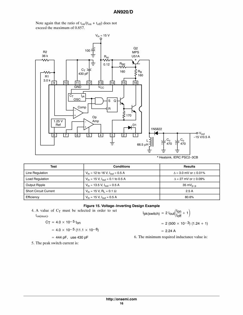
AN920/D
http://onsemi.com16
Note again that the ratio of ton/(ton + toff) does notexceed the maximum of 0.857.
9
8
10
7
11
6
12
5
13
4
14
3
15
2
16
1
1.25 VRef
CT IpkOSC
+
−
D1
170
+
−
S
R
Q
OpAmp
Comp
GND VCC
Co470
Vout−15 V/0.5 A
L66.5 μH
+100
CT430 pF
Rsc
0.12
Vin = 15 V
R13.0 k
R236 k
RB160
RBE
160
+
Co470+
1N5822
* Heatsink, IERC PSC2−3CB
Q2MPSU51A
*
Test Conditions Results
Line Regulation Vin = 12 to 16 V, Iout = 0.5 A Δ = 3.0 mV or ± 0.01%
Load Regulation Vin = 15 V, Iout = 0.1 to 0.5 A Δ = 27 mV or ± 0.09%
Output Ripple Vin = 13.5 V, Iout = 0.5 A 35 mVp−p
Short Circuit Current Vin = 15 V, RL = 0.1 Ω 2.5 A
Efficiency Vin = 15 V, Iout = 0.5 A 80.6%
Figure 15. Voltage−Inverting Design Example4. A value of CT must be selected in order to set
ton(max).
CT � 4.0 � 10− 5 ton
� 4.0 � 10− 5 (11.1 � 10− 6)
� 444 pF, use 430 pF
5. The peak switch current is:
Ipk(switch) � 2 Iout�tontoff
� 1�� 2 (500 � 10− 3) (1.24 � 1)
� 2.24 A
6. The minimum required inductance value is:
AN920/D
http://onsemi.com17
Lmin � �Vin(min) � VsatIpk(switch)
� ton
� �13.5 � 0.82.24
� 11.1 � 10− 6
� 66.5 �H
7. The current−limit resistor value was selected bydetermining the level of Ipk(switch) for Vin = 16.5 V.
Ipk(switch) � �Vin � VsatLmin
� ton
� � 16.5 � 0.866.5 � 10− 6
� 11.1 � 10− 6
� 2.62 A
Rsc � 0.33Ipk(switch)
� 0.332.62
� 0.13 �, use 0.12 �
8. An approximate value for an ideal output filtercapacitor is:
Co � IoutVripple(p−p)
� ton
0.560 � 10− 3
11.1 � 10− 6
92.5 �F
The ripple contribution due to the gain of thecomparator is:
Vripple(p−p) �|Vout|
Vref1.5 � 10− 3
� 151.25
1.5 � 10− 3
� 18 mV
For a given level of ripple, the ESR of the output filtercapacitor becomes the dominant factor in choosinga value for capacitance. Therefore two 470 μFcapacitors with an ESR of 0.020 Ω each was chosen.The ripple voltage due to the capacitance value is5.9 mV and 22.4 mV due to ESR. This yields a totalripple voltage of:
Eripple(p−p) �|Vout|
Vref1.5 � 10− 3 �
IoutCo
ton � Ipk ESR
� 18 mV � 5.9 mV � 22.4 mV
� 46.3 mV
9. The nominal output voltage is programmed by theR1, R2 divider. Note that with a negative outputvoltage, the inverting input of the comparator isreferenced to ground. Therefore, the voltage at thejunction of R1, R2 and the noninverting input must
also be at ground potential when Vout is in regulation.The magnitude of Vout is:
|Vout| � 1.25 R2R1
A divider current of about 400 μA was desired forthis example.
R1 � 1.25400 � 10− 6
� 3,125 �, use 3.0 k
R2 �|Vout|1.25
R1Then
� 151.25
3.0 � 10− 3
� 36 k
10. Output switch transistor Q2 is driven into a softsaturation with a forced gain of 35 at an input voltageof 13.5 V in order to enhance the turn−off switchingtime. The required base drive is:
IB �Ipk(switch)
Bf
� 2.2435
� 64 mA
The value for the base−emitter turn−off resistor RBEis determined by:
RBE �10 Bf
Ipk(switch)
�10 (35)
2.24
� 156.3 �, use 160 �
The additional base current required due to RBE is:
IRBE �VBE (Q2)
RBE
� 0.8160
� 5.0 mA
Then IB (Q2) is equal to the sum of 64 mA + 5.0 mA= 69 mA. Allow 0.8 V for the IC driver saturationand 0.3 V for the drop across Rsc (0.12 × 2.24 A Ipk).Then the base driver resistor is equal to:
RB �Vin(min) � Vsat(IC) � VRSC � VBE(Q2)
IB � I160 �
� 13.5 � 0.8 � 0.3 � 1.0(64 � 5) � 10− 3
� 165.2 �, use 160 �
AN920/D
http://onsemi.com18
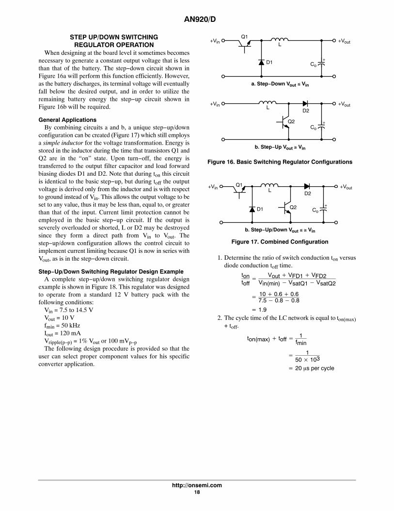
STEP UP/DOWN SWITCHINGREGULATOR OPERATION
When designing at the board level it sometimes becomesnecessary to generate a constant output voltage that is lessthan that of the battery. The step−down circuit shown inFigure 16a will perform this function efficiently. However,as the battery discharges, its terminal voltage will eventuallyfall below the desired output, and in order to utilize theremaining battery energy the step−up circuit shown inFigure 16b will be required.
General ApplicationsBy combining circuits a and b, a unique step−up/down
configuration can be created (Figure 17) which still employsa simple inductor for the voltage transformation. Energy isstored in the inductor during the time that transistors Q1 andQ2 are in the “on” state. Upon turn−off, the energy istransferred to the output filter capacitor and load forwardbiasing diodes D1 and D2. Note that during ton this circuitis identical to the basic step−up, but during toff the outputvoltage is derived only from the inductor and is with respectto ground instead of Vin. This allows the output voltage to beset to any value, thus it may be less than, equal to, or greaterthan that of the input. Current limit protection cannot beemployed in the basic step−up circuit. If the output isseverely overloaded or shorted, L or D2 may be destroyedsince they form a direct path from Vin to Vout. Thestep−up/down configuration allows the control circuit toimplement current limiting because Q1 is now in series withVout, as is in the step−down circuit.
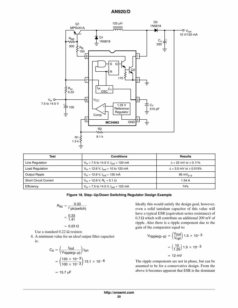
Step−Up/Down Switching Regulator Design ExampleA complete step−up/down switching regulator design
example is shown in Figure 18. This regulator was designedto operate from a standard 12 V battery pack with thefollowing conditions:
Vin = 7.5 to 14.5 VVout = 10 Vfmin = 50 kHzIout = 120 mAVripple(p−p) = 1% Vout or 100 mVp−pThe following design procedure is provided so that the
user can select proper component values for his specificconverter application.
Figure 16. Basic Switching Regulator Configurations
+Vin +Vout
+Co
L
D1
Q1
+Vin +VoutLD2
Q2
a. Step−Down Vout � Vin
b. Step−Up Vout � Vin
+Co
Figure 17. Combined Configuration
+Vin +VoutLD2
Q2
b. Step−Up/Down Vout � � Vin
+Co
Q1
D1
1. Determine the ratio of switch conduction ton versusdiode conduction toff time.
tontoff
� Vout � VFD1 � VFD2Vin(min) � VsatQ1 � VsatQ2
� 10 � 0.6 � 0.67.5 � 0.8 � 0.8
� 1.92. The cycle time of the LC network is equal to ton(max)
+ toff.
ton(max) � toff �1
fmin
� 150 � 103
� 20 �s per cycle
AN920/D
http://onsemi.com19
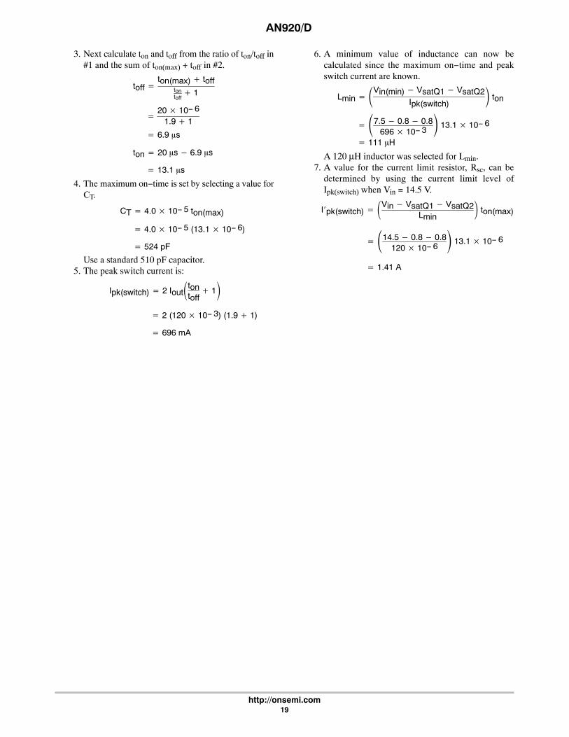
3. Next calculate ton and toff from the ratio of ton/toff in#1 and the sum of ton(max) + toff in #2.
toff �ton(max) � toff
tontoff
� 1
�20 � 10− 6
1.9 � 1
� 6.9 �s
ton � 20 �s � 6.9 �s
� 13.1 �s
4. The maximum on−time is set by selecting a value forCT.
CT � 4.0 � 10− 5 ton(max)
� 4.0 � 10− 5 (13.1 � 10− 6)
� 524 pF
Use a standard 510 pF capacitor.5. The peak switch current is:
Ipk(switch) � 2 Iout�tontoff
� 1�� 2 (120 � 10− 3) (1.9 � 1)
� 696 mA
6. A minimum value of inductance can now becalculated since the maximum on−time and peakswitch current are known.
Lmin � �Vin(min) � VsatQ1 � VsatQ2Ipk(switch)
� ton
� �7.5 � 0.8 � 0.8696 � 10− 3
� 13.1 � 10− 6
� 111 �H
A 120 μH inductor was selected for Lmin.7. A value for the current limit resistor, Rsc, can be
determined by using the current limit level ofIpk(switch) when Vin = 14.5 V.
Ipk(switch) � �Vin � VsatQ1 � VsatQ2Lmin
� ton(max)
� �14.5 � 0.8 � 0.8120 � 10− 6
� 13.1 � 10− 6
� 1.41 A
AN920/D
http://onsemi.com20
RBE
300
8
7
6
5
1
2
3
4
Q2
S
R
Q
Ipk CTOSC
+
−
1.25 VReferenceRegulator
Comp
VCCVin7.5 to 14.5 V
120 μH
CT510 pF
R11.3 k
D11N5818 Co
330
Vout10 V/120 mA
MC34063 GND
170
RB150
+
Rsc0.22
100
R2
9.1 k
D21N5818
+
Q1MPSU51A
Test Conditions Results
Line Regulation Vin = 7.5 to 14.5 V, Iout = 120 mA Δ = 22 mV or ± 0.11%
Load Regulation Vin = 12.6 V, Iout = 10 to 120 mA Δ = 3.0 mV or ± 0.015%
Output Ripple Vin = 12.6 V, Iout = 120 mA 95 mVp−p
Short Circuit Current Vin = 12.6 V, RL = 0.1 Ω 1.54 A
Efficiency Vin = 7.5 to 14.5 V, Iout = 120 mA 74%
Figure 18. Step−Up/Down Switching Regulator Design Example
Rsc � 0.33Ipk(switch)
� 0.331.41
� 0.23 �
Use a standard 0.22 Ω resistor.8. A minimum value for an ideal output filter capacitor
is:
Co � IoutVripple(p−p)
� ton
�120 � 10− 3
100 � 10− 3� 13.1 � 10− 6
15.7 �F
Ideally this would satisfy the design goal, however,even a solid tantalum capacitor of this value willhave a typical ESR (equivalent series resistance) of0.3 Ω which will contribute an additional 209 mV ofripple. Also there is a ripple component due to thegain of the comparator equal to:
Vripple(p−p) � �VoutVref� 1.5 � 10− 3
� � 101.25
� 1.5 � 10− 3
� 12 mV
The ripple components are not in phase, but can beassumed to be for a conservative design. From theabove it becomes apparent that ESR is the dominant
AN920/D
http://onsemi.com21
factor in the selection of an output filter capacitor. A330 μF with an ESR of 0.12 Ω was selected to satisfythis design example by the following:
ESR Vripple(p−p) � �Iout
Co� ton � �Vout
VRef� 1.5 � 10− 3
Ipk(switch)
9. The nominal output voltage is programmed by theR1, R2 resistor divider.
R2 � R1 �VoutVRef
� 1�
� R1 � 101.25
� 1�� 7 R1
If 1.3 k is chosen for R1, then R2 would be 9.1 k, bothbeing standard resistor values.
10. Transistor Q1 is driven into saturation with a forcedgain of approximately 20 at an input voltage of 7.5 V.The required base drive is:
IB �Ipk(switch)
Bf
�696 � 10− 3
20
� 35 mA
The value for the base−emitter turn−off resistor RBEis determined by:
RBE �10 Bf
Ipk(switch)
�10 (20)
696 � 10− 3
� 287 �
A standard 300 Ω resistor was selected.The additional base current required due to RBE is:
IRBE �VBEQ1
RBE
� 0.8300
� 3.0 mA
The base drive resistor for Q1 is equal to:
RB �Vin(min) � Vsat(driver) � VRSC � VBEQ1
IB � IRBE
� 7.5 � 0.8 � 0.15 � 0.8(35 � 3) � 10− 3
� 151 �
A standard 150 Ω resistor was used.The circuit performance data shows excellent line and
load regulation. There is some loss in conversion efficiencyover the basic step−up or step−down circuits due to theadded switch transistor and diode “on” losses. However, thisunique converter demonstrates that with a simple inductor,a step−up/down converter with current limiting can beconstructed.
DESIGN CONSIDERATIONSAs previously stated, the design equations for Lmin were
based upon the assumption that the switching regulator isoperating on the onset of continuous conduction with a fixedinput voltage, maximum output load current, and aminimum charge−current oscillator. Typically the oscillatorcharge−current will be greater than the specific minimum of20 microamps, thus ton will be somewhat shorter and theactual LC operating frequency will be greater than predicted.
Also note that the voltage drop developed across thecurrent−limit resistor Rsc was not accounted for in the ton/toffand Lmin design formulas. This voltage drop must beconsidered when designing high current converters thatoperate with an input voltage of less than 5.0 V.
When checking the initial switcher operation with anoscilloscope, there will be some concern of circuit instabilitydue to the apparent random switching of the output. Theoscilloscope will be difficult to synchronize. This is not aproblem. It is a normal operating characteristic of this typeof switching regulator and is caused by the asynchronousoperation of the comparator to that of the oscillator. Theoscilloscope may be synchronized by varying the inputvoltage or load current slightly from the design nominals.
High frequency circuit layout techniques are imperativewith switching regulators. To minimize EMI, all highcurrent loops should be kept as short as possible using heavycopper runs. The low current signal and high current switchand output grounds should return on separate paths back tothe input filter capacitor. The R1, R2 output voltage dividershould be located as close to the IC as possible to eliminateany noise pick−up into the feedback loop. The circuitdiagrams were purposely drawn in a manner to depict this.
All circuits used molypermalloy power toroid cores forthe magnetics where only the inductance value is given. Thenumber of turns, wire and core size information is not givensince no attempt was made to optimize their design. Inductorand transformer design information may be obtained fromthe magnetic core and assembly companies listed on theswitching regulator component source table.
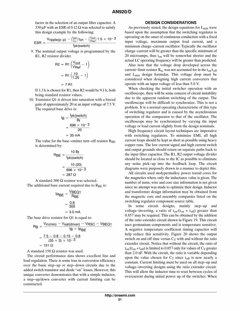
In some circuit designs, mainly step−up andvoltage−inverting, a ratio of ton/(ton + toff) greater than0.857 may be required. This can be obtained by the additionof the ratio extender circuit shown in Figure 19. This circuituses germanium components and is temperature sensitive.A negative temperature coefficient timing capacitor willhelp reduce this sensitivity. Figure 20 shows the outputswitch on and off time versus CT with and without the ratioextender circuit. Notice that without the circuit, the ratio ofton/(ton + toff) is limited to 0.857 only for values of CT greaterthan 2.0 nF. With the circuit, the ratio is variable dependingupon the value chosen for CT since toff is now nearly aconstant. Current limiting must be used on all step−up andvoltage−inverting designs using the ratio extender circuit.This will allow the inductor time to reset between cycles ofovercurrent during initial power up of the switcher. When
AN920/D
http://onsemi.com22
the output filter capacitor reaches its nominal voltage, thevoltage feedback loop will control regulation.
Figure 19. Output Switch On−Off Time Test Circuit
8
7
6
5
1
2
3
4
S
R
Q
Ipk CTOSC
+
−
1.25 VReferenceRegulator
Comp
VCC
Vin = 5 V
CT
170
10
1N270
+
To Scope
100
2N524
tontoff
RatioExtenderCircuit
ton
toff
Figure 20. Output Switch On−Off Time versusOscillator Timing Capacitor
0
1000
t on−
t off,
Out
put S
witc
h O
n−O
ff Ti
me
(μs)
0
CT, Oscillator Timing Capacitor (nF)
1.0 10 100
100
10
ton
Without Ratio Extender CircuitWith Ratio Extender Circuit
Comparator Noninverting Input = VrefComparator Inverting Input = GNDVCC = 5 V; Ipk(sense) = VCCTA = 25°C
tontoff
toff
AN920/D
http://onsemi.com23
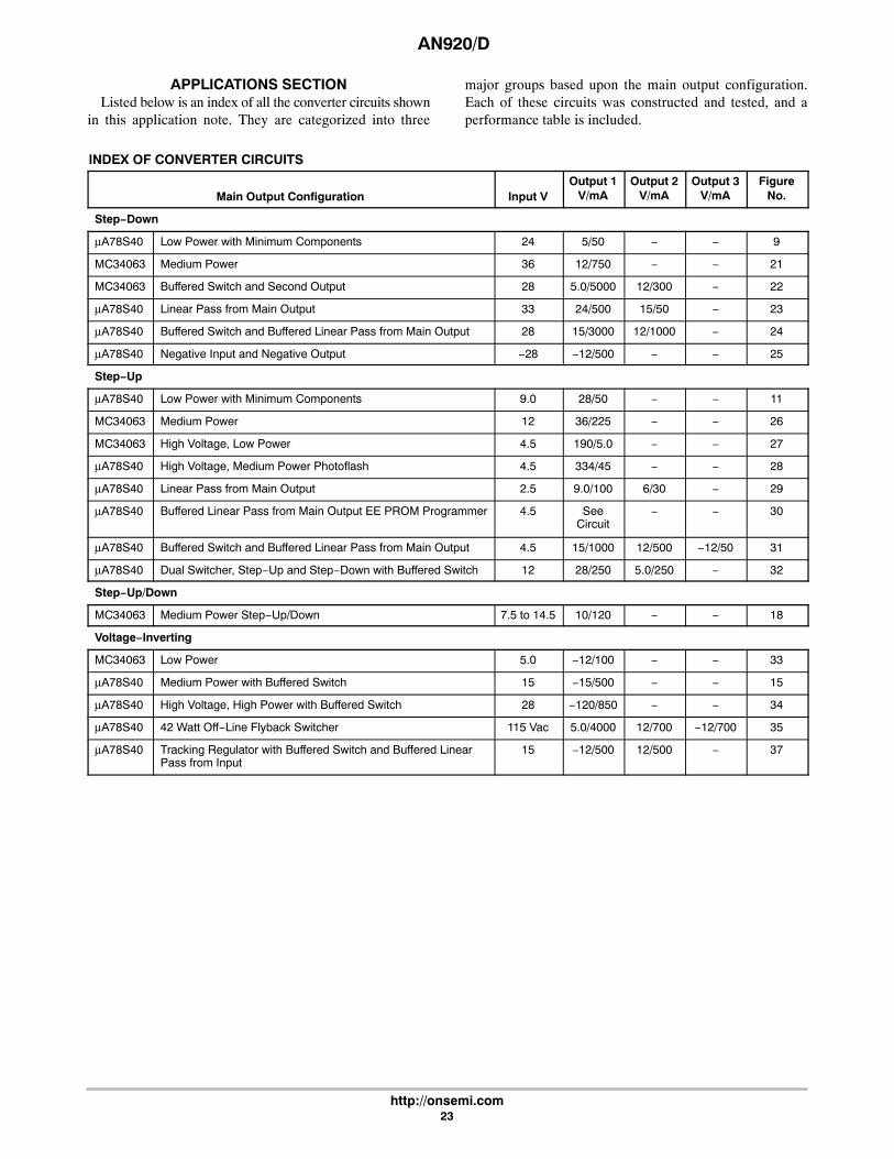
APPLICATIONS SECTIONListed below is an index of all the converter circuits shown
in this application note. They are categorized into three
major groups based upon the main output configuration.Each of these circuits was constructed and tested, and aperformance table is included.
INDEX OF CONVERTER CIRCUITS
Main Output Configuration Input VOutput 1
V/mAOutput 2
V/mAOutput 3
V/mAFigure
No.
Step−Down
μA78S40 Low Power with Minimum Components 24 5/50 − − 9
MC34063 Medium Power 36 12/750 − − 21
MC34063 Buffered Switch and Second Output 28 5.0/5000 12/300 − 22
μA78S40 Linear Pass from Main Output 33 24/500 15/50 − 23
μA78S40 Buffered Switch and Buffered Linear Pass from Main Output 28 15/3000 12/1000 − 24
μA78S40 Negative Input and Negative Output −28 −12/500 − − 25
Step−Up
μA78S40 Low Power with Minimum Components 9.0 28/50 − − 11
MC34063 Medium Power 12 36/225 − − 26
MC34063 High Voltage, Low Power 4.5 190/5.0 − − 27
μA78S40 High Voltage, Medium Power Photoflash 4.5 334/45 − − 28
μA78S40 Linear Pass from Main Output 2.5 9.0/100 6/30 − 29
μA78S40 Buffered Linear Pass from Main Output EE PROM Programmer 4.5 SeeCircuit
− − 30
μA78S40 Buffered Switch and Buffered Linear Pass from Main Output 4.5 15/1000 12/500 −12/50 31
μA78S40 Dual Switcher, Step−Up and Step−Down with Buffered Switch 12 28/250 5.0/250 − 32
Step−Up/Down
MC34063 Medium Power Step−Up/Down 7.5 to 14.5 10/120 − − 18
Voltage−Inverting
MC34063 Low Power 5.0 −12/100 − − 33
μA78S40 Medium Power with Buffered Switch 15 −15/500 − − 15
μA78S40 High Voltage, High Power with Buffered Switch 28 −120/850 − − 34
μA78S40 42 Watt Off−Line Flyback Switcher 115 Vac 5.0/4000 12/700 −12/700 35
μA78S40 Tracking Regulator with Buffered Switch and Buffered LinearPass from Input
15 −12/500 12/500 − 37
AN920/D
http://onsemi.com24
8
7
6
5
1
2
3
4
S
R
Q
Ipk CTOSC
+
−
1.25 VReferenceRegulator
Comp
VCCVin36 V 190 μH
470 pF
1.74 k
1N5819
47
Vout12 V/750 mA
GND
170
15 k
+
0.2
270+
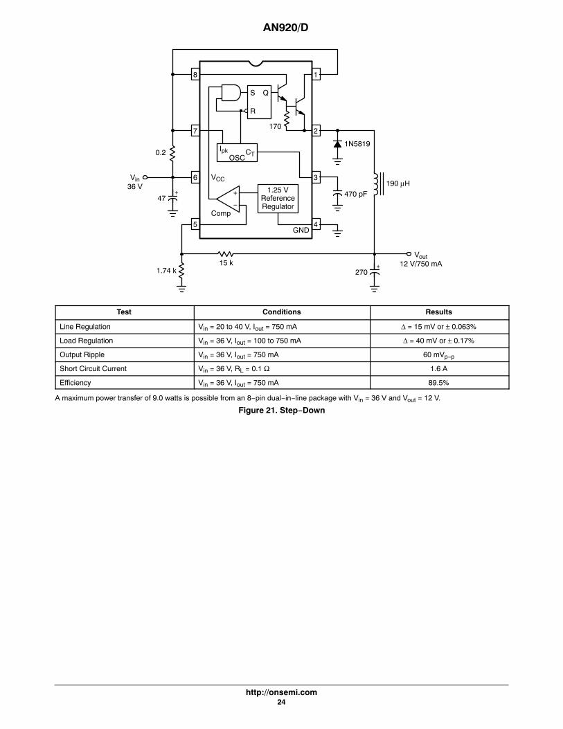
Test Conditions Results
Line Regulation Vin = 20 to 40 V, Iout = 750 mA Δ = 15 mV or ± 0.063%
Load Regulation Vin = 36 V, Iout = 100 to 750 mA Δ = 40 mV or ± 0.17%
Output Ripple Vin = 36 V, Iout = 750 mA 60 mVp−p
Short Circuit Current Vin = 36 V, RL = 0.1 Ω 1.6 A
Efficiency Vin = 36 V, Iout = 750 mA 89.5%
A maximum power transfer of 9.0 watts is possible from an 8−pin dual−in−line package with Vin = 36 V and Vout = 12 V.
Figure 21. Step−Down
AN920/D
http://onsemi.com25
8
7
6
5
1
2
3
4
S
R
Q
Ipk CTOSC
+
−
1.25 VReferenceRegulator
Comp
VCCVin28 V
23.1 μH
330 pF
1.2 k
MBR2540 (2)
2200
Vout15 V/5 A
GND
170
3.6 k
+
0.036
100
22
51
D45VH4 (1)
T
22,000+
1.4T
1N5819
Vout212 V/300 m A
470+
(1) Heatsink, IERC HP3−T0127−CB(2) Heatsink, IERC UP−000−CB
Test Conditions Results
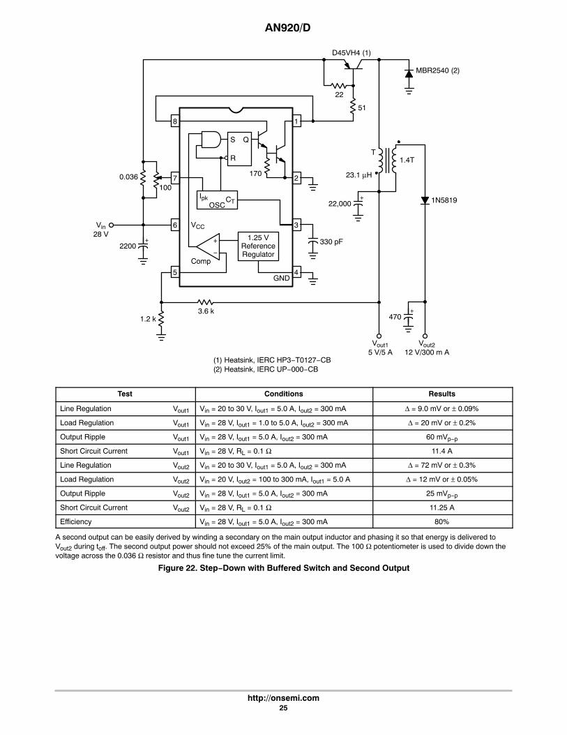
Line Regulation Vout1 Vin = 20 to 30 V, Iout1 = 5.0 A, Iout2 = 300 mA Δ = 9.0 mV or ± 0.09%
Load Regulation Vout1 Vin = 28 V, Iout1 = 1.0 to 5.0 A, Iout2 = 300 mA Δ = 20 mV or ± 0.2%
Output Ripple Vout1 Vin = 28 V, Iout1 = 5.0 A, Iout2 = 300 mA 60 mVp−p
Short Circuit Current Vout1 Vin = 28 V, RL = 0.1 Ω 11.4 A
Line Regulation Vout2 Vin = 20 to 30 V, Iout1 = 5.0 A, Iout2 = 300 mA Δ = 72 mV or ± 0.3%
Load Regulation Vout2 Vin = 20 V, Iout2 = 100 to 300 mA, Iout1 = 5.0 A Δ = 12 mV or ± 0.05%
Output Ripple Vout2 Vin = 28 V, Iout1 = 5.0 A, Iout2 = 300 mA 25 mVp−p
Short Circuit Current Vout2 Vin = 28 V, RL = 0.1 Ω 11.25 A
Efficiency Vin = 28 V, Iout1 = 5.0 A, Iout2 = 300 mA 80%
A second output can be easily derived by winding a secondary on the main output inductor and phasing it so that energy is delivered toVout2 during toff. The second output power should not exceed 25% of the main output. The 100 Ω potentiometer is used to divide down thevoltage across the 0.036 Ω resistor and thus fine tune the current limit.
Figure 22. Step−Down with Buffered Switch and Second Output
AN920/D
http://onsemi.com26
9
8
10
7
11
6
12
5
13
4
14
3
15
2
16
1
1.25 VRef
CT IpkOSC
+
−
D1
170
+
−
S
R
Q
OpAmp
Comp
GND VCC
1N5819 +100
Vout215 V/50 mA
+33
750 pF
0.221.0 k18.2 k
Vin = 33 V
1.8 k22 k
2.0 k
Vout124 V/500 mA
130 μH0.1
Test Conditions Results
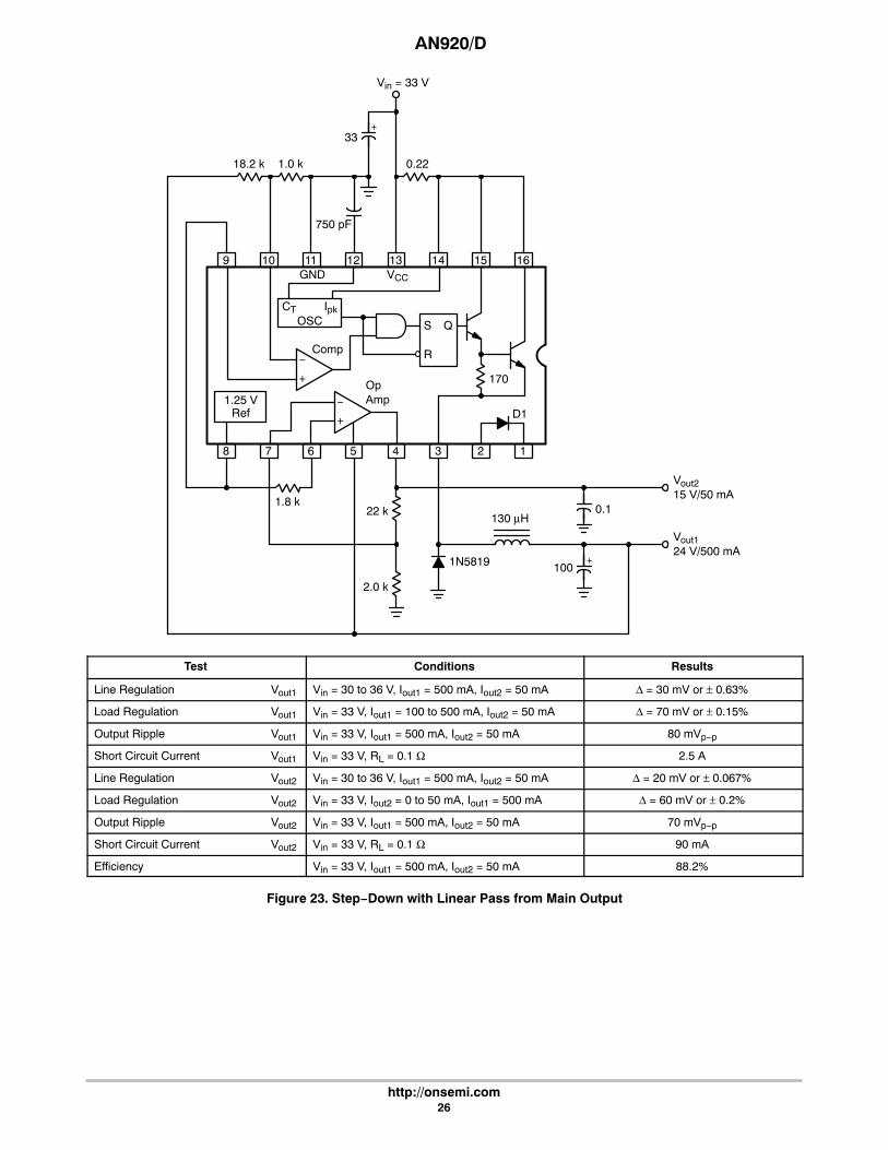
Line Regulation Vout1 Vin = 30 to 36 V, Iout1 = 500 mA, Iout2 = 50 mA Δ = 30 mV or ± 0.63%
Load Regulation Vout1 Vin = 33 V, Iout1 = 100 to 500 mA, Iout2 = 50 mA Δ = 70 mV or ± 0.15%
Output Ripple Vout1 Vin = 33 V, Iout1 = 500 mA, Iout2 = 50 mA 80 mVp−p
Short Circuit Current Vout1 Vin = 33 V, RL = 0.1 Ω 2.5 A
Line Regulation Vout2 Vin = 30 to 36 V, Iout1 = 500 mA, Iout2 = 50 mA Δ = 20 mV or ± 0.067%
Load Regulation Vout2 Vin = 33 V, Iout2 = 0 to 50 mA, Iout1 = 500 mA Δ = 60 mV or ± 0.2%
Output Ripple Vout2 Vin = 33 V, Iout1 = 500 mA, Iout2 = 50 mA 70 mVp−p
Short Circuit Current Vout2 Vin = 33 V, RL = 0.1 Ω 90 mA
Efficiency Vin = 33 V, Iout1 = 500 mA, Iout2 = 50 mA 88.2%
Figure 23. Step−Down with Linear Pass from Main Output
AN920/D
http://onsemi.com27
9
8
10
7
11
6
12
5
13
4
14
3
15
2
16
1
1.25 VRef
CT IpkOSC
+
−
D1
170
+
−
S
R
Q
OpAmp
Comp
GND VCC
35 μH
910 pF
Vin = 28 to 36 V
51
MBR1540*
*All devices mounted on one heatsink, extra #10 hole required forMBR2540, IERC HP3−T0127−4CB
D45VH10* Vout1
15 V/3.0 mA
820
8.2 k
963
Vout212 V/1.0 mA
0.1
TIP31 *
+470
0.022
100
22 k 2.0 k
+2200
Test Conditions Results
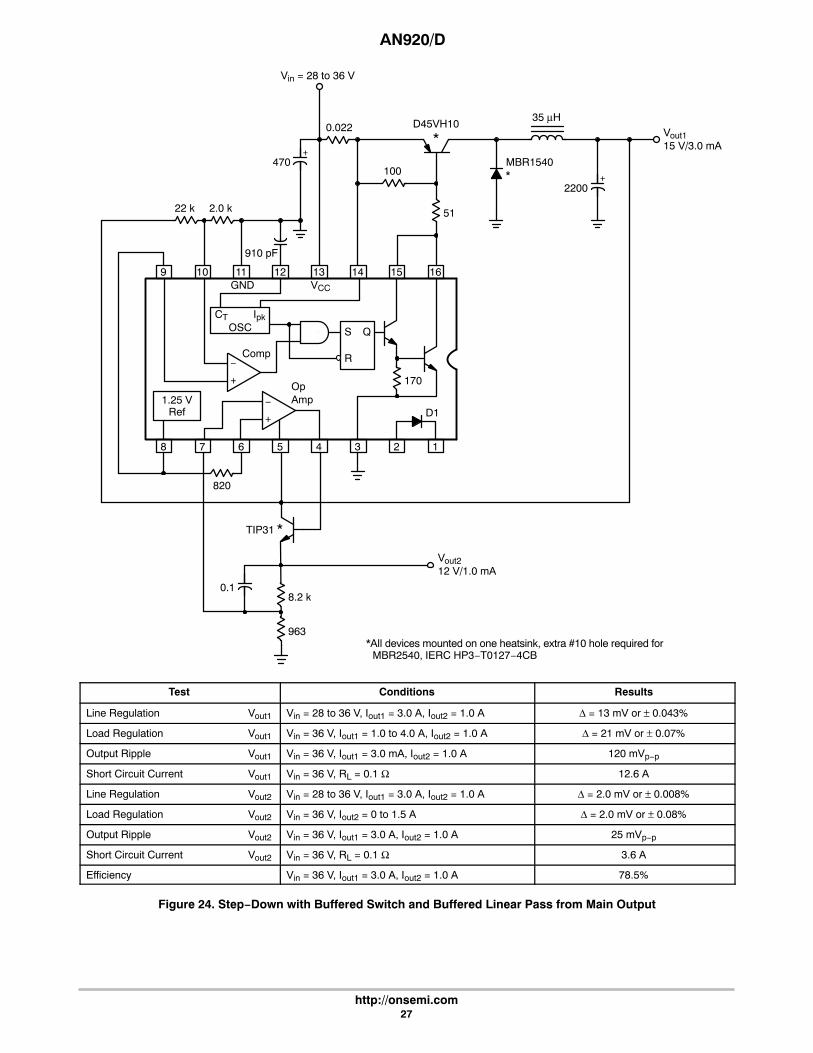
Line Regulation Vout1 Vin = 28 to 36 V, Iout1 = 3.0 A, Iout2 = 1.0 A Δ = 13 mV or ± 0.043%
Load Regulation Vout1 Vin = 36 V, Iout1 = 1.0 to 4.0 A, Iout2 = 1.0 A Δ = 21 mV or ± 0.07%
Output Ripple Vout1 Vin = 36 V, Iout1 = 3.0 mA, Iout2 = 1.0 A 120 mVp−p
Short Circuit Current Vout1 Vin = 36 V, RL = 0.1 Ω 12.6 A
Line Regulation Vout2 Vin = 28 to 36 V, Iout1 = 3.0 A, Iout2 = 1.0 A Δ = 2.0 mV or ± 0.008%
Load Regulation Vout2 Vin = 36 V, Iout2 = 0 to 1.5 A Δ = 2.0 mV or ± 0.08%
Output Ripple Vout2 Vin = 36 V, Iout1 = 3.0 A, Iout2 = 1.0 A 25 mVp−p
Short Circuit Current Vout2 Vin = 36 V, RL = 0.1 Ω 3.6 A
Efficiency Vin = 36 V, Iout1 = 3.0 A, Iout2 = 1.0 A 78.5%
Figure 24. Step−Down with Buffered Switch and Buffered Linear Pass from Main Output
AN920/D
http://onsemi.com28
9
8
10
7
11
6
12
5
13
4
14
3
15
2
16
1
1.25 VRef
CT IpkOSC
+
−
D1
170
+
−
S
R
Q
OpAmp
Comp
GND VCC
1N5819820 pF
Vin = −28 V
11.8 k 3.09 k
470
+ 100
Vout−12 V/500 mA
275 μH
+ 470
470 20 k 10 k
10 k 20 k
−2.5 V
Test Conditions Results
Line Regulation Vin = −22 to −28 V, Iout = 500 mA Δ = 25 mV or ± 0.104%
Load Regulation Vin = −28 V, Iout = 100 to 500 mA Δ = 10 mV or ± 0.042%
Output Ripple Vin = −28 V, Iout = 500 mA 130 mVp−p
Efficiency Vin = −28 V, Iout = 500 mA 85.5%
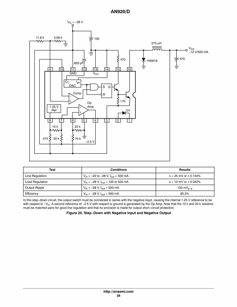
In this step−down circuit, the output switch must be connected in series with the negative input, causing the internal 1.25 V reference to bewith respect to −Vin. A second reference of −2.5 V with respect to ground is generated by the Op Amp. Note that the 10 k and 20 k resistorsmust be matched pairs for good line regulation and that no provision is made for output short−circuit protection.
Figure 25. Step−Down with Negative Input and Negative Output
AN920/D
http://onsemi.com29
8
7
6
5
1
2
3
4
S
R
Q
Ipk CTOSC
+
−
1.25 VReferenceRegulator
Comp
VCCVin12 V
180 μH
910 pF
2.7 k
1N5819
470
Vout36 V/225 mA
GND
170
75 k
0.22
100
7.75T T1.25 V
+
Test Conditions Results
Line Regulation Vin = 11 to 15 V, Iout = 225 mA Δ = 20 mV or ± 0.028%
Load Regulation Vin = 12 V, Iout = 50 to 225 mA Δ = 30 mV or ± 0.042%
Output Ripple Vin = 12 V, Iout = 225 mA 100 mVp−p
Efficiency Vin = 12 V, Iout = 225 mA 90.4%
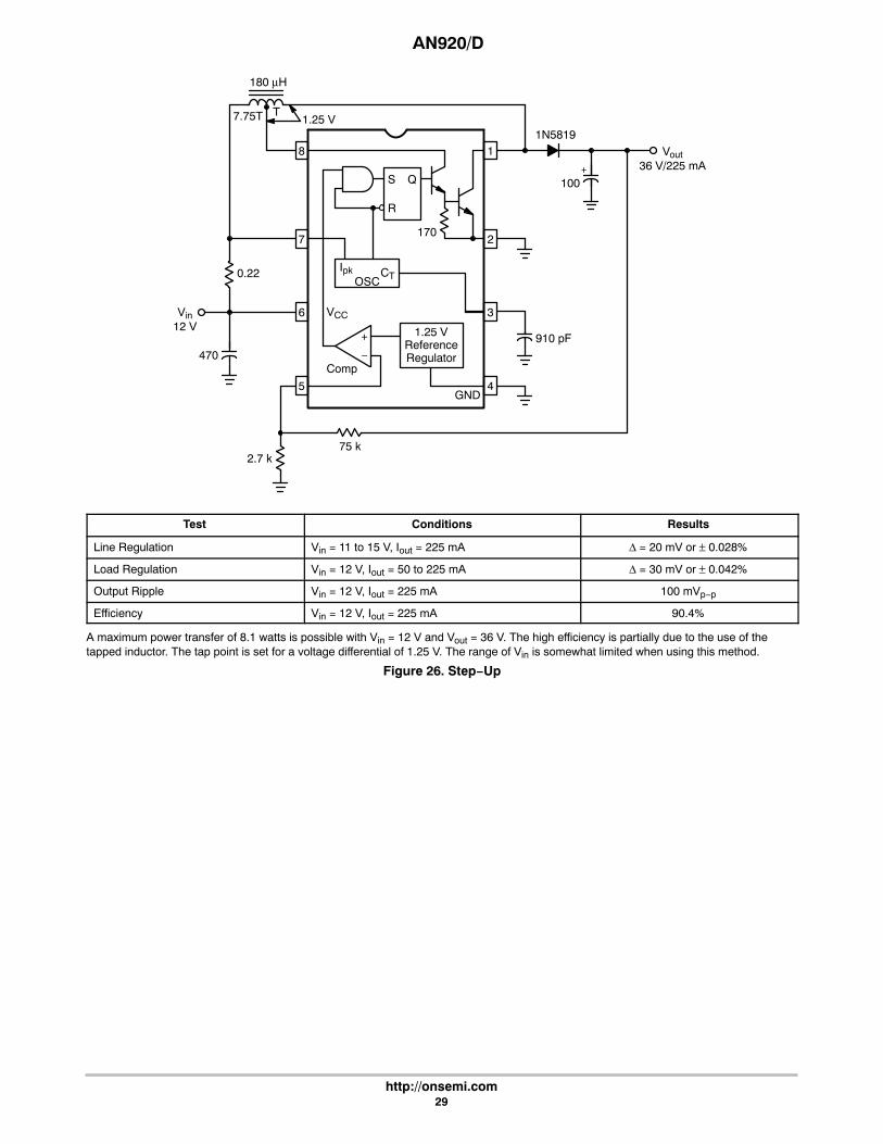
A maximum power transfer of 8.1 watts is possible with Vin = 12 V and Vout = 36 V. The high efficiency is partially due to the use of thetapped inductor. The tap point is set for a voltage differential of 1.25 V. The range of Vin is somewhat limited when using this method.
Figure 26. Step−Up
AN920/D
http://onsemi.com30
Primary = 25 Turns #28 AWGSecondary = 260 Turns #40 AWGCore = Ferroxcube 1408P−L00−3CBBobbin = Ferroxcube 1408PCB1Gap = 0.003″ Spacer for a primary inductance of 140 μH.
8
7
6
5
1
2
3
4
S
R
Q
Ipk CTOSC
+
−
1.25 VReferenceRegulator
Comp
VCCVin4.5 to12 V
680 pF
27 k
1N4936
100
GND
170
4.7 M
0.24
1.0+
+
10 k
Vout190 V/5.0 mA
To SCD 504 DisplayLp = 140 μH
T1
T1:
Test Conditions Results
Line Regulation Vin = 4.5 to 12 V, Iout = 5.0 mA Δ = 2.3 V or ± 0.61%
Load Regulation Vin = 5.0 V, Iout = 1.0 to 6.0 mA Δ = 1.4 V or ± 0.37%
Output Ripple Vin = 5.0 V, Iout = 5.0 mA 250 mVp−p
Short Circuit Current Vin = 5.0 V, RL = 0.1 Ω 113 mA
Efficiency Vin = 5.0 V, Iout = 5.0 mA 68%
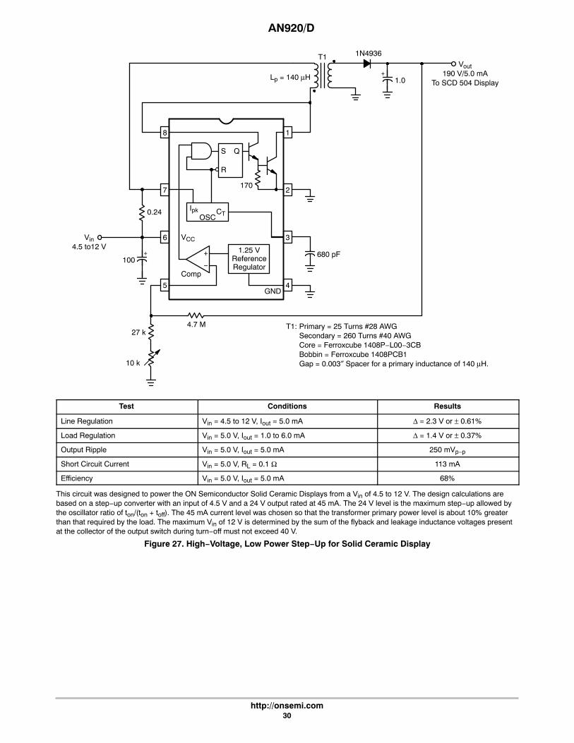
This circuit was designed to power the ON Semiconductor Solid Ceramic Displays from a Vin of 4.5 to 12 V. The design calculations arebased on a step−up converter with an input of 4.5 V and a 24 V output rated at 45 mA. The 24 V level is the maximum step−up allowed bythe oscillator ratio of ton/(ton + toff). The 45 mA current level was chosen so that the transformer primary power level is about 10% greaterthan that required by the load. The maximum Vin of 12 V is determined by the sum of the flyback and leakage inductance voltages presentat the collector of the output switch during turn−off must not exceed 40 V.
Figure 27. High−Voltage, Low Power Step−Up for Solid Ceramic Display
AN920/D
http://onsemi.com31
9
8
10
7
11
6
12
5
13
4
14
3
15
2
16
1
1.25 VRef
CT IpkOSC
+
−
D1
170
+
−
S
R
Q
OpAmp
Comp
GND VCC
Vin = 4.5 to 6.0 V
5.1
MR817
D45VH10*
18 k
18 k
1600 pF
+2200
0.022
27
+C1500
1.8 M
4.7 M
120
ChargingIndicatorLED
Primary = 10 Turns #17 AWGSecondary = 130 Turns #30 AWGCore = Ferroxcube 2616P−L00−3C8Bobbin = Ferroxcube 2616PCB1Gap = 0.018″ Spacer for a Primary
Inductance of 16.5 μH.
T1:
Lp =16.5 μH
T1
* Heatsink, IERC PB1−36CB
22 M
10
0.033
Shu
tter
G.E.FT−118
TRAIDPL−10
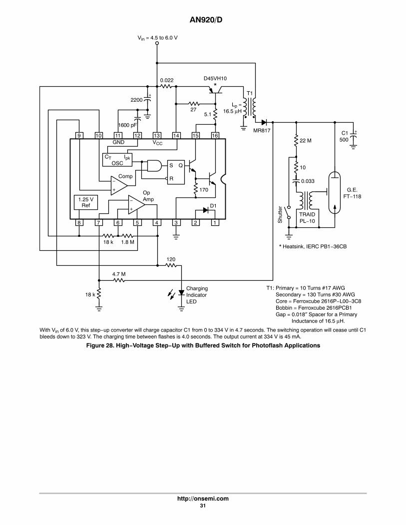
With Vin of 6.0 V, this step−up converter will charge capacitor C1 from 0 to 334 V in 4.7 seconds. The switching operation will cease until C1bleeds down to 323 V. The charging time between flashes is 4.0 seconds. The output current at 334 V is 45 mA.
Figure 28. High−Voltage Step−Up with Buffered Switch for Photoflash Applications
AN920/D
http://onsemi.com32
9
8
10
7
11
6
12
5
13
4
14
3
15
2
16
1
1.25 VRef
CT IpkOSC
+
−
D1
170
+
−
S
R
Q
OpAmp
Comp
GND VCC
0.1
Vout19.0 V/100 mA
+470
910 pF
0.2210 k62 k
Vin = 2.5 V
8.2 k
38.3 k
10 k
Vout26.0 V/30 mA
27
40 μH1N5819
+330
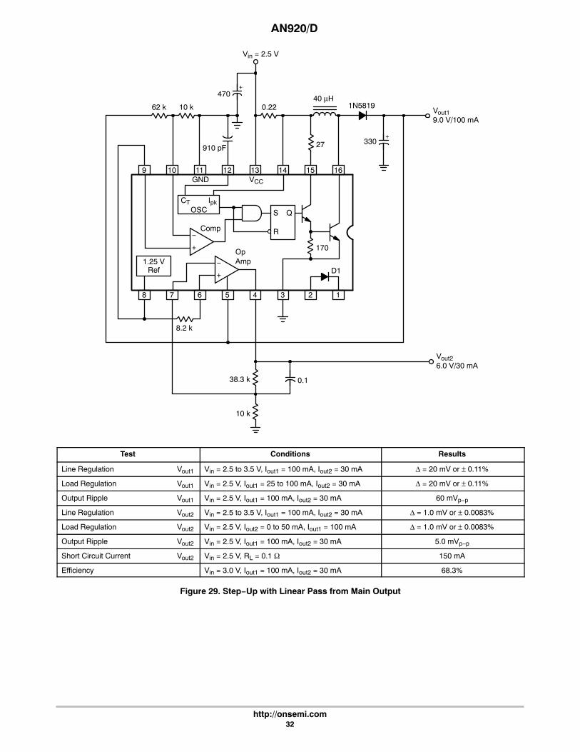
Test Conditions Results
Line Regulation Vout1 Vin = 2.5 to 3.5 V, Iout1 = 100 mA, Iout2 = 30 mA Δ = 20 mV or ± 0.11%
Load Regulation Vout1 Vin = 2.5 V, Iout1 = 25 to 100 mA, Iout2 = 30 mA Δ = 20 mV or ± 0.11%
Output Ripple Vout1 Vin = 2.5 V, Iout1 = 100 mA, Iout2 = 30 mA 60 mVp−p
Line Regulation Vout2 Vin = 2.5 to 3.5 V, Iout1 = 100 mA, Iout2 = 30 mA Δ = 1.0 mV or ± 0.0083%
Load Regulation Vout2 Vin = 2.5 V, Iout2 = 0 to 50 mA, Iout1 = 100 mA Δ = 1.0 mV or ± 0.0083%
Output Ripple Vout2 Vin = 2.5 V, Iout1 = 100 mA, Iout2 = 30 mA 5.0 mVp−p
Short Circuit Current Vout2 Vin = 2.5 V, RL = 0.1 Ω 150 mA
Efficiency Vin = 3.0 V, Iout1 = 100 mA, Iout2 = 30 mA 68.3%
Figure 29. Step−Up with Linear Pass from Main Output
AN920/D
http://onsemi.com33
9
8
10
7
11
6
12
5
13
4
14
3
15
2
16
1
1.25 VRef
CT IpkOSC
+
−
D1
170
+
−
S
R
Q
OpAmp
Comp
GND VCC
0.058
+47
820 pF
0.22
294 k
Vin = 4.5 to 5.5 V
1.0 k
68
70 μH
+1.0
13.7 k
16.5 k‘A’
‘B’
4.7 k 470+
VPP Output
10.2 k
3.4 k
470
47 k
57.6 k
16.5 k
‘X’ TIP29
WRITETTL Input
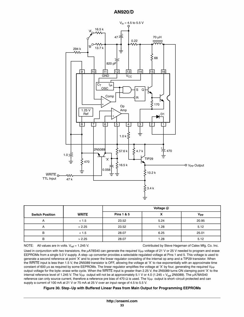
2N5089
Switch Position WRITE
Voltage @
Pins 1 & 5 X VPP
A < 1.5 23.52 5.24 20.95
A > 2.25 23.52 1.28 5.12
B < 1.5 28.07 6.25 25.01
B > 2.25 28.07 1.28 5.12
NOTE: All values are in volts. Vref = 1.245 V. Contributed by Steve Hageman of Calex Mfg. Co. Inc.
Used in conjunction with two transistors, the μA78S40 can generate the required VPP voltage of 21 V or 25 V needed to program and eraseEEPROMs from a single 5.0 V supply. A step−up converter provides a selectable regulated voltage at Pins 1 and 5. This voltage is used togenerate a second reference at point ‘X’ and to power the linear regulator consisting of the internal op amp and a TIP29 transistor. Whenthe WRITE input is less than 1.5 V, the 2N5089 transistor is OFF, allowing the voltage at ‘X’ to rise exponentially with an approximate timeconstant of 600 μs as required by some EEPROMs. The linear regulator amplifies the voltage at ‘X’ by four, generating the required VPPoutput voltage for the byte−erase write cycle. When the WRITE input is greater than 2.25 V, the 2N5089 turns ON clamping point ‘X’ to theinternal reference level of 1.245 V. The VPP output will not be at approximately 5.1 V or 4.0 (1.245 + Vsat 2N5089). The μA78AS40reference can only source current, therefore a reference pre bias of 470 Ω is used. The VPP output is short−circuit protected and cansupply a current of 100 mA at 21 V or 75 mA at 25 V over an input range of 4.5 to 5.5 V.
Figure 30. Step−Up with Buffered Linear Pass from Main Output for Programming EEPROMs
AN920/D
http://onsemi.com34
9
8
10
7
11
6
12
5
13
4
14
3
15
2
16
1
1.25 VRef
CT IpkOSC
+
−
D1
170
+
−
S
R
Q
OpAmp
Comp
GND VCC
Vout115 V/1.0 mA
+6800
1200 pF
0.0222.0 k22 k
Vin = 4.5 to 5.5 V
820
27
5.1 8.8 μH
2N5824+
2200
8.2 k
953
0.1
TIP29(2)
D44VH1(1)
+
47
1N5818
1N5818
+ 47
MC79L12ACP Vout3
−12 V/50 mA
0.1
Vout2−12 V/50 mA
+47
(1) Heatsink, IERC LAT0127B5CB(2) Heatsink, IERC PB1−36CB
Test Conditions Results
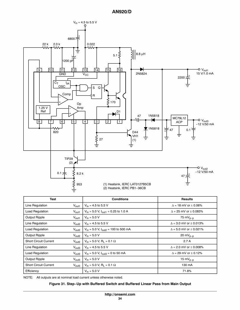
Line Regulation Vout1 Vin = 4.5 to 5.5 V Δ = 18 mV or ± 0.06%
Load Regulation Vout1 Vin = 5.0 V, Iout1 = 0.25 to 1.0 A Δ = 25 mV or ± 0.083%
Output Ripple Vout1 Vin = 5.0 V 75 mVp−p
Line Regulation Vout2 Vin = 4.5 to 5.5 V Δ = 3.0 mV or ± 0.013%
Load Regulation Vout2 Vin = 5.0 V, Iout2 = 100 to 500 mA Δ = 5.0 mV or ± 0.021%
Output Ripple Vout2 Vin = 5.0 V 20 mVp−p
Short Circuit Current Vout2 Vin = 5.0 V, RL = 0.1 Ω 2.7 A
Line Regulation Vout3 Vin = 4.5 to 5.5 V Δ = 2.0 mV or ± 0.008%
Load Regulation Vout3 Vin = 5.0 V, Iout3 = 0 to 50 mA Δ = 29 mV or ± 0.12%
Output Ripple Vout3 Vin = 5.0 V 15 mVp−p
Short Circuit Current Vout3 Vin = 5.0 V, RL = 0.1 Ω 130 mA
Efficiency Vin = 5.0 V 71.8%
NOTE: All outputs are at nominal load current unless otherwise noted.
Figure 31. Step−Up with Buffered Switch and Buffered Linear Pass from Main Output
AN920/D
http://onsemi.com35
9
8
10
7
11
6
12
5
13
4
14
3
15
2
16
1
1.25 VRef
CT IpkOSC
+
−
D1
170
+
−
S
R
Q
OpAmp
Comp
GND VCC
0.1
Vout128 V/250 mA
+47
470 pF
0.24
2.2 k
Vin = 12 V
100
1.2 k
180
108 μH
1N5819 +470
47 k
10 k
470Vout2
5.0 V/250 mA1N5819
4.4 mH
+2200
1.0 M
3.6 k
MPSU51A
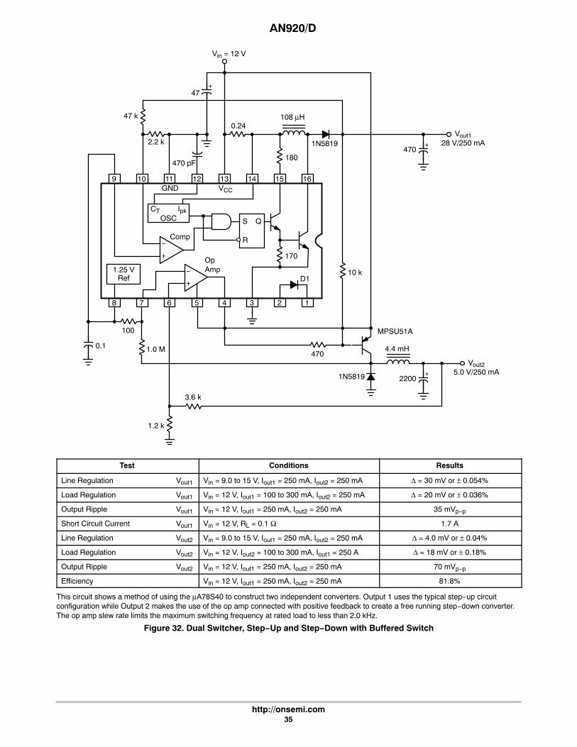
Test Conditions Results
Line Regulation Vout1 Vin = 9.0 to 15 V, Iout1 = 250 mA, Iout2 = 250 mA Δ = 30 mV or ± 0.054%
Load Regulation Vout1 Vin = 12 V, Iout1 = 100 to 300 mA, Iout2 = 250 mA Δ = 20 mV or ± 0.036%
Output Ripple Vout1 Vin = 12 V, Iout1 = 250 mA, Iout2 = 250 mA 35 mVp−p
Short Circuit Current Vout1 Vin = 12 V, RL = 0.1 Ω 1.7 A
Line Regulation Vout2 Vin = 9.0 to 15 V, Iout1 = 250 mA, Iout2 = 250 mA Δ = 4.0 mV or ± 0.04%
Load Regulation Vout2 Vin = 12 V, Iout2 = 100 to 300 mA, Iout1 = 250 A Δ = 18 mV or ± 0.18%
Output Ripple Vout2 Vin = 12 V, Iout1 = 250 mA, Iout2 = 250 mA 70 mVp−p
Efficiency Vin = 12 V, Iout1 = 250 mA, Iout2 = 250 mA 81.8%
This circuit shows a method of using the μA78S40 to construct two independent converters. Output 1 uses the typical step−up circuitconfiguration while Output 2 makes the use of the op amp connected with positive feedback to create a free running step−down converter.The op amp slew rate limits the maximum switching frequency at rated load to less than 2.0 kHz.
Figure 32. Dual Switcher, Step−Up and Step−Down with Buffered Switch
AN920/D
http://onsemi.com36
8
7
6
5
1
2
3
4
S
R
Q
Ipk CTOSC
+
−
1.25 VReferenceRegulator
Comp
VCCVin4.5 to 6.0 V
R28.2 k
1N5819
100
Vout−12 V/100 mA
GND
170
R1953
+
0.24
1000+
88 μH
1300 pF+
|Vout| � 1.25 �1 � R2R1�
Test Conditions Results
Line Regulation Vin = 4.5 to 5.0 V, Iout = 100 mA Δ = 2.0 mV or ± 0.008%
Load Regulation Vin = 5.0 V, Iout = 10 to 100 mA Δ = 10 mV or ± 0.042%
Output Ripple Vin = 5.0 V, Iout = 100 mA 35 mVp−p
Short Circuit Current Vin = 5.0 V, RL = 0.1 Ω 1.4 A
Efficiency Vin = 5.0 V, Iout = 100 mA 60%
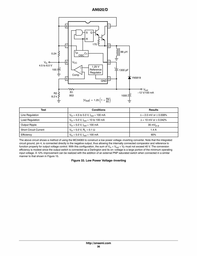
The above circuit shows a method of using the MC34063 to construct a low power voltage−inverting converter. Note that the integratedcircuit ground, pin 4, is connected directly to the negative output, thus allowing the internally connected comparator and reference tofunction properly for output voltage control. With this configuration, the sum of Vin + Vout + VF must not exceed 40 V. The conversionefficiency is modest since the output switch is connected as a Darlington and its on−voltage is a large portion of the minimum operatinginput voltage. A 12% improvement can be realized with the addition of an external PNP saturated switch when connected in a similarmanner to that shown in Figure 15.
Figure 33. Low Power Voltage−Inverting
AN920/D
http://onsemi.com37
9
8
10
7
11
6
12
5
13
4
14
3
15
2
16
1
1.25 VRef
CT IpkOSC
+
−
D1
170
+
−
S
R
Q
OpAmp
Comp
GND VCC
+4700
1200 pF
Vin = 28 V
Vout−120 V/850 mA
MR822
+ 560
1050
100 k
1000pF
100
Rsc0.022
10
51
200 μH Center Tapped
*HeatsinkIERC Nested Pair
HP1−T03−CBHP3−T03−CB
2N6438*
Test Conditions Results
Line Regulation Vin = 24 to 28 V, Iout = 850 mA Δ = 100 mV or ± 0.042%
Load Regulation Vin = 28 V, Iout = 100 to 850 mA Δ = 70 mV or ± 0.029%
Output Ripple Vin = 28 V, Iout = 850 mA 450 mVp−p
Short Circuit Current Vin = 28 V, RL = 0.1 Ω 6.4 A
Efficiency Vin = 28 V, Iout = 850 mA 81.8%
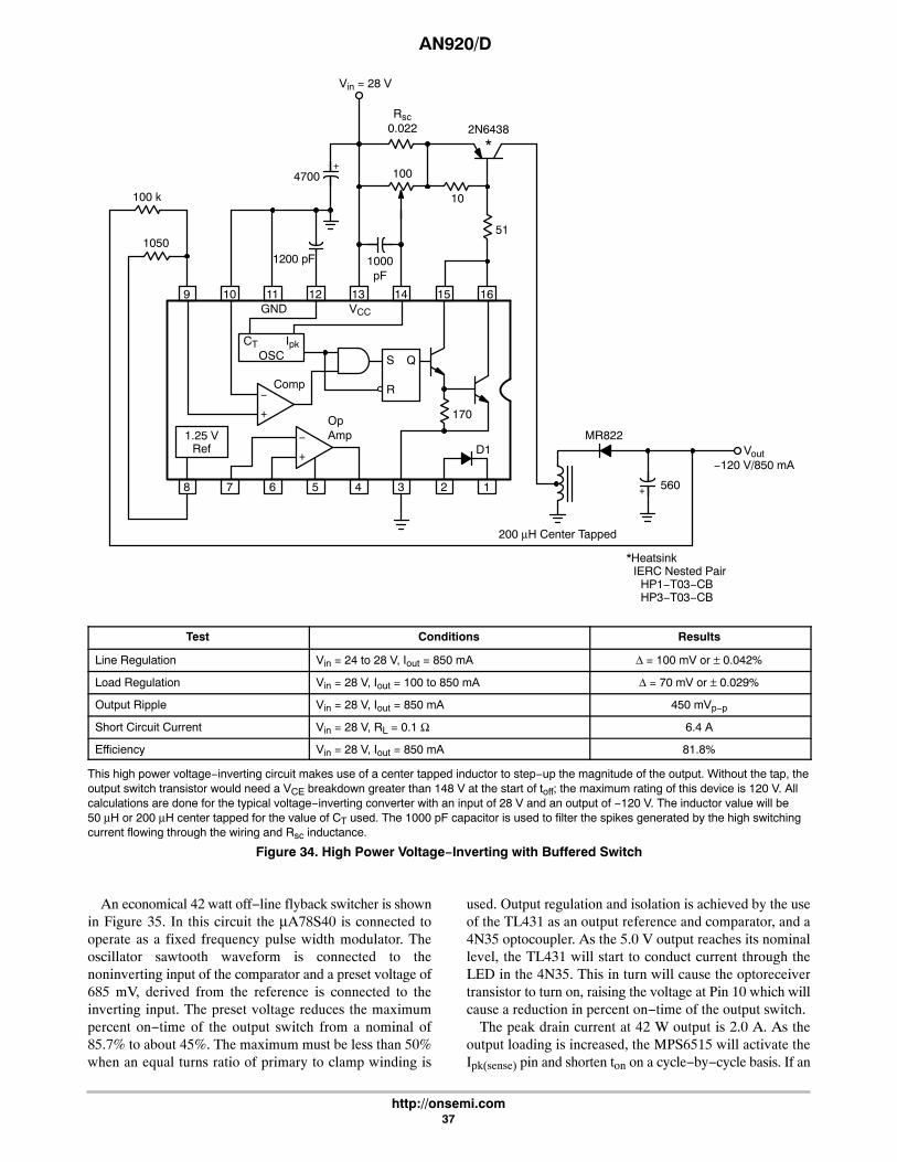
This high power voltage−inverting circuit makes use of a center tapped inductor to step−up the magnitude of the output. Without the tap, theoutput switch transistor would need a VCE breakdown greater than 148 V at the start of toff; the maximum rating of this device is 120 V. Allcalculations are done for the typical voltage−inverting converter with an input of 28 V and an output of −120 V. The inductor value will be 50 μH or 200 μH center tapped for the value of CT used. The 1000 pF capacitor is used to filter the spikes generated by the high switchingcurrent flowing through the wiring and Rsc inductance.
Figure 34. High Power Voltage−Inverting with Buffered Switch
An economical 42 watt off−line flyback switcher is shownin Figure 35. In this circuit the μA78S40 is connected tooperate as a fixed frequency pulse width modulator. Theoscillator sawtooth waveform is connected to thenoninverting input of the comparator and a preset voltage of685 mV, derived from the reference is connected to theinverting input. The preset voltage reduces the maximumpercent on−time of the output switch from a nominal of85.7% to about 45%. The maximum must be less than 50%when an equal turns ratio of primary to clamp winding is
used. Output regulation and isolation is achieved by the useof the TL431 as an output reference and comparator, and a4N35 optocoupler. As the 5.0 V output reaches its nominallevel, the TL431 will start to conduct current through theLED in the 4N35. This in turn will cause the optoreceivertransistor to turn on, raising the voltage at Pin 10 which willcause a reduction in percent on−time of the output switch.
The peak drain current at 42 W output is 2.0 A. As theoutput loading is increased, the MPS6515 will activate theIpk(sense) pin and shorten ton on a cycle−by−cycle basis. If an
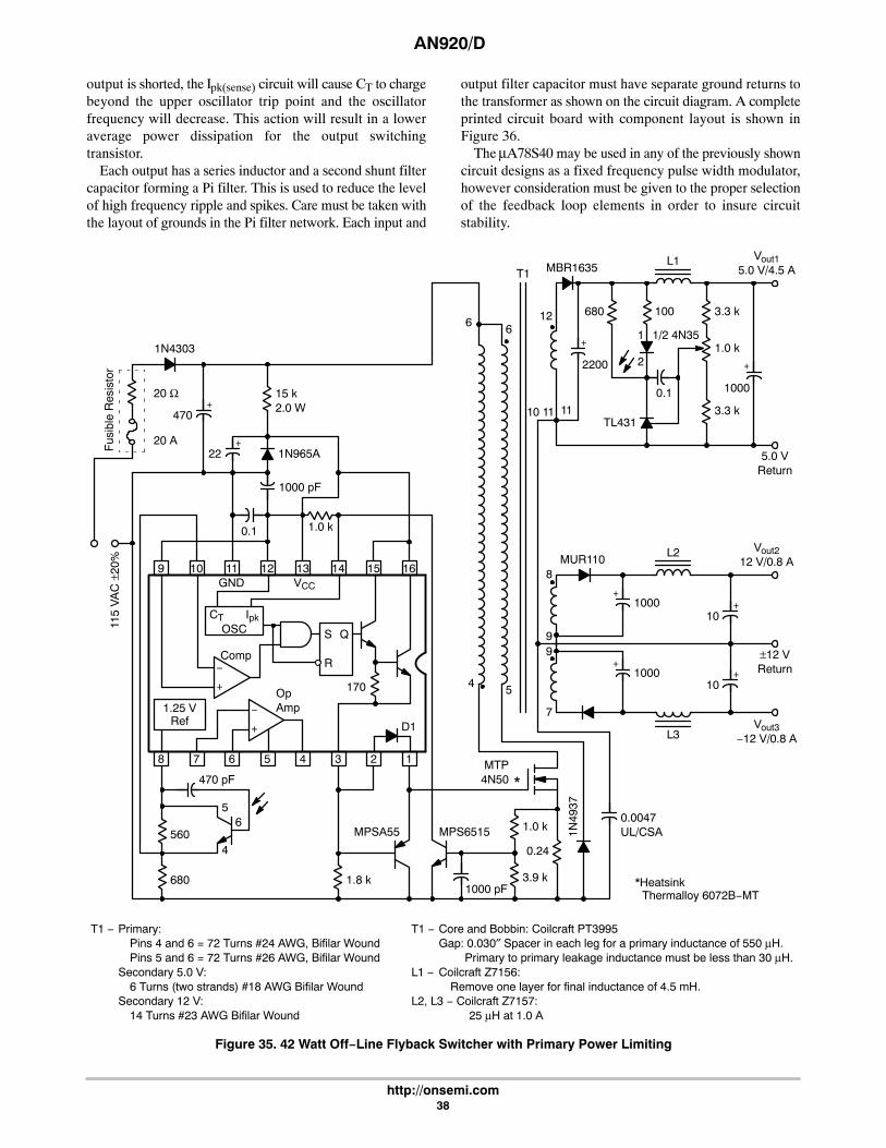
AN920/D
http://onsemi.com38
output is shorted, the Ipk(sense) circuit will cause CT to chargebeyond the upper oscillator trip point and the oscillatorfrequency will decrease. This action will result in a loweraverage power dissipation for the output switchingtransistor.
Each output has a series inductor and a second shunt filtercapacitor forming a Pi filter. This is used to reduce the levelof high frequency ripple and spikes. Care must be taken withthe layout of grounds in the Pi filter network. Each input and
output filter capacitor must have separate ground returns tothe transformer as shown on the circuit diagram. A completeprinted circuit board with component layout is shown inFigure 36.
The μA78S40 may be used in any of the previously showncircuit designs as a fixed frequency pulse width modulator,however consideration must be given to the proper selectionof the feedback loop elements in order to insure circuitstability.
9
8
10
7
11
6
12
5
13
4
14
3
15
2
16
1
1.25 VRef
CT IpkOSC
+
−
D1
170
+
−
S
R
Q
OpAmp
Comp
GND VCC
+
115
VA
C ±
20%
Fus
ible
Res
isto
r
20 Ω
20 A
+470
22
15 k2.0 W
1000 pF
0.1 1.0 k
1N965A
1N4303
680
560
470 pF
5
4
6
1.8 k
MPSA55 MPS6515
1000 pF3.9 k
1.0 k
0.24
1N49
37
*MTP4N50
0.0047UL/CSA
45
66
T1
+
12
10 11 11
2200
680
MBR1635
+
1000
100
L1
1
2
TL431
0.1
1.0 k
3.3 k
3.3 k
1/2 4N35
Vout15.0 V/4.5 A
5.0 VReturn
Vout212 V/0.8 A
±12 VReturn
Vout3−12 V/0.8 A
MUR1108
99
7
+1000
+1000
L2
L3
+10
+10
*HeatsinkThermalloy 6072B−MT
T1 − Primary:Pins 4 and 6 = 72 Turns #24 AWG, Bifilar WoundPins 5 and 6 = 72 Turns #26 AWG, Bifilar Wound
Secondary 5.0 V:6 Turns (two strands) #18 AWG Bifilar Wound
Secondary 12 V:14 Turns #23 AWG Bifilar Wound
T1 − Core and Bobbin: Coilcraft PT3995Gap: 0.030″ Spacer in each leg for a primary inductance of 550 μH.
Primary to primary leakage inductance must be less than 30 μH.L1 − Coilcraft Z7156:
Remove one layer for final inductance of 4.5 mH.L2, L3 − Coilcraft Z7157:
25 μH at 1.0 A
Figure 35. 42 Watt Off−Line Flyback Switcher with Primary Power Limiting

AN920/D
http://onsemi.com39
Test Conditions Results
Line Regulation Vout1 Vin = 92 to 138 Vac Δ = 1.0 mV or ± 0.01%
Load Regulation Vout1 Vin = 115 Vac, Iout1 = 1.0 to 4.5 A Δ = 3.0 mV or ± 0.03%
Output Ripple Vout1 Vin = 115 Vac 40 mVp−p
Short Circuit Current Vout1 Vin = 115 Vac, RL = 0.1 Ω 19.2 A
Line Regulation Vout2 or Vout3 Vin = 92 to 138 Vac Δ = 10 mV or ± 0.04%
Load Regulation Vout2 or Vout3 Vin = 115 Vac, Iout2 or Iout3 = 0.25 to 0.8 A Δ = 384 mV or ± 1.6%
Output Ripple Vout2 or Vout3 Vin = 115 Vac 80 mVp−p
Short Circuit Current Vout2 or Vout3 Vin = 115 Vac, RL = 0.1 Ω 10.8 A
Efficiency Vin = 115 Vac 75.7%
NOTE: All outputs are at nominal load current unless otherwise noted.
Figure 35. (continued) 42 Watt Off−Line Flyback Switcher with Primary Power Limiting
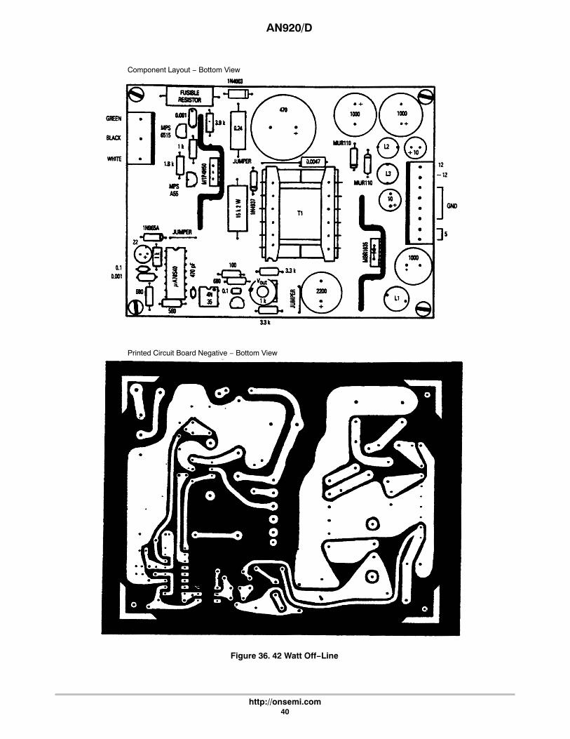
AN920/D
http://onsemi.com40
Figure 36. 42 Watt Off−Line
Component Layout − Bottom View
Printed Circuit Board Negative − Bottom View
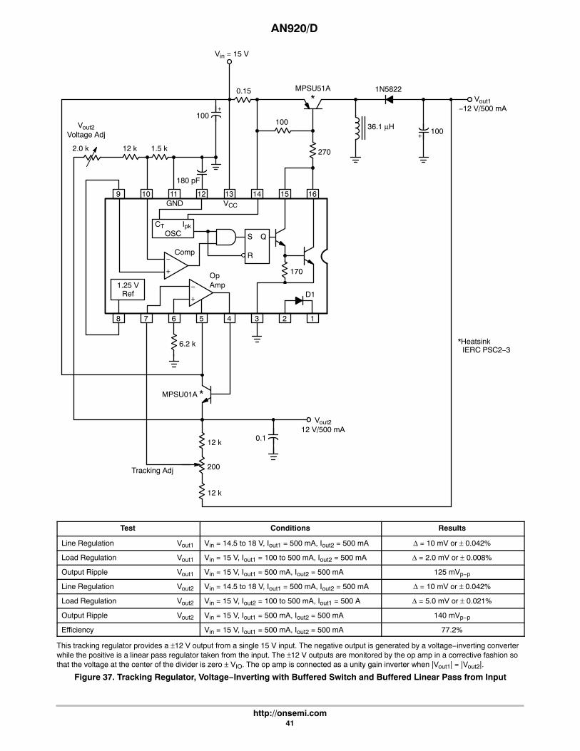
AN920/D
http://onsemi.com41
9
8
10
7
11
6
12
5
13
4
14
3
15
2
16
1
1.25 VRef
CT IpkOSC
+
−
D1
170
+
−
S
R
Q
OpAmp
Comp
GND VCC
36.1 μH
180 pF
Vin = 15 V
270
1N5822
*HeatsinkIERC PSC2−3
MPSU51A* Vout1
−12 V/500 mA
12 k
200
Vout212 V/500 mA
0.1
MPSU01A *
+100
0.15
100
12 k 1.5 k
+ 100
6.2 k
2.0 k
Vout2Voltage Adj
12 k
Tracking Adj
Test Conditions Results
Line Regulation Vout1 Vin = 14.5 to 18 V, Iout1 = 500 mA, Iout2 = 500 mA Δ = 10 mV or ± 0.042%
Load Regulation Vout1 Vin = 15 V, Iout1 = 100 to 500 mA, Iout2 = 500 mA Δ = 2.0 mV or ± 0.008%
Output Ripple Vout1 Vin = 15 V, Iout1 = 500 mA, Iout2 = 500 mA 125 mVp−p
Line Regulation Vout2 Vin = 14.5 to 18 V, Iout1 = 500 mA, Iout2 = 500 mA Δ = 10 mV or ± 0.042%
Load Regulation Vout2 Vin = 15 V, Iout2 = 100 to 500 mA, Iout1 = 500 A Δ = 5.0 mV or ± 0.021%
Output Ripple Vout2 Vin = 15 V, Iout1 = 500 mA, Iout2 = 500 mA 140 mVp−p
Efficiency Vin = 15 V, Iout1 = 500 mA, Iout2 = 500 mA 77.2%
This tracking regulator provides a ±12 V output from a single 15 V input. The negative output is generated by a voltage−inverting converterwhile the positive is a linear pass regulator taken from the input. The ±12 V outputs are monitored by the op amp in a corrective fashion sothat the voltage at the center of the divider is zero ± VIO. The op amp is connected as a unity gain inverter when |Vout1| = |Vout2|.
Figure 37. Tracking Regulator, Voltage−Inverting with Buffered Switch and Buffered Linear Pass from Input
AN920/D
http://onsemi.com42
SUMMARYThe goal of this application note is to convey the theory of
operation of the MC34063 and μA78S40, and to show thederivation of the basic first order design equations. Thecircuits were chosen to explore a variety of cost effective andpractical solutions in designing switching converters.Another major objective is to show the ease and simplicityin designing switching converters and to remove anymystical “black magic” fears. ON Semiconductor maintainsa Linear and Discrete products applications staff that isdedicated to assisting customers with any design problemsor questions.
BIBLIOGRAPHY
Steve Hageman, DC/dc Converter Powers EEPROMs,EDN, January 20, 1983.
Design Manual for SMPS Power Transformers, Copyright1982 by Pulse Engineering.
HeatSink/Dissipator Products and Thermal ManagementGuide, Copyright 1980 by International ElectronicResearch Corporation.
Linear and Interface Integrated Circuits Data Manual,Copyright 1988 by Motorola Inc.
Linear Ferrite Materials and Components Sixth Edition, byFerroxcube Corporation.
Linear/Switchmode Voltage Regulator Hanbook Theory andPractice, Copyright 1989 by Motorola Inc.
Molypermalloy Powder Cores, Catalog MPP−303U,Copyright 1981 by Magnetics Inc.
Motorola Power Data Book, Copyright 1989 by MotorolaInc.
Motorola Rectifiers and Zener Diodes Data Book,Copyright 1988 by Motorola Inc.
Structured Design of Switching Power Magnetics,AN−P100, by Coilcraft Inc.
Switching and Linear Power Supply, Power ConverterDesign, by Abraham I. Pressman, Copyright 1977 byHayden Book Company Inc.
�A78S40 Switching Voltage Regulator, Application Note370, Copyright 1982 by Fairchild Camera andInstruments Corporation.
Switchmode Transformer Ferrite E−Core Packages,DS−P200, by Coilcraft Inc.
Jim Lange, Tapped Inductor Improves Efficiency forSwitching Regulator, ED 16, August 2, 1979.
Voltage Regulator Handbook, Copyright 1978 by FairchildCamera and Instruments Corporation.
SWITCHING REGULATORCOMPONENT SOURCES
CapacitorErie Technical ProductsP.O. Box 961Erie, PA 16512(814) 452−5611
Mallory Capacitor Co.P.O. Box 1284Indianapolis, IN 46206(317) 856−3731
United Chemi−Con9801 W. Higgins RoadRosemont, IL 60018(312) 696−2000
HeatsinksIERC135 W. Magnolia Blvd.Burbank, CA(213) 849−2481
Thermalloy, Inc.2021 W. Valley View LaneDallas, Texas 75234(214) 243−4321
Magnetic AssembliesCoilcraft, Inc.1102 Silver Lake Rd.Cary, IL 60013(312) 639−2361
Pulse EngineeringP.O. Box 12235San Diego, CA 92112(714) 279−5900
Magnetic CoresFerroxcube5083 Kings HighwaySaugerties, NY 12477(914) 246−2811
Magnetics, Inc.P.O. Box 391Butler, PA 16001(412) 282−8282
TDK Corporation of America4709 Golf Rd., Suite 300Skokie, IL 60076(312) 679−8200
ON Semiconductor does not endorse or warrant thesuppliers referenced.
AN920/D
http://onsemi.com43
ON Semiconductor and are registered trademarks of Semiconductor Components Industries, LLC (SCILLC). SCILLC owns the rights to a number of patents, trademarks,copyrights, trade secrets, and other intellectual property. A listing of SCILLC’s product/patent coverage may be accessed at www.onsemi.com/site/pdf/Patent−Marking.pdf. SCILLCreserves the right to make changes without further notice to any products herein. SCILLC makes no warranty, representation or guarantee regarding the suitability of its products for anyparticular purpose, nor does SCILLC assume any liability arising out of the application or use of any product or circuit, and specifically disclaims any and all liability, including withoutlimitation special, consequential or incidental damages. “Typical” parameters which may be provided in SCILLC data sheets and/or specifications can and do vary in different applicationsand actual performance may vary over time. All operating parameters, including “Typicals” must be validated for each customer application by customer’s technical experts. SCILLCdoes not convey any license under its patent rights nor the rights of others. SCILLC products are not designed, intended, or authorized for use as components in systems intended forsurgical implant into the body, or other applications intended to support or sustain life, or for any other application in which the failure of the SCILLC product could create a situation wherepersonal injury or death may occur. Should Buyer purchase or use SCILLC products for any such unintended or unauthorized application, Buyer shall indemnify and hold SCILLC andits officers, employees, subsidiaries, affiliates, and distributors harmless against all claims, costs, damages, and expenses, and reasonable attorney fees arising out of, directly or indirectly,any claim of personal injury or death associated with such unintended or unauthorized use, even if such claim alleges that SCILLC was negligent regarding the design or manufactureof the part. SCILLC is an Equal Opportunity/Affirmative Action Employer. This literature is subject to all applicable copyright laws and is not for resale in any manner.
PUBLICATION ORDERING INFORMATIONN. American Technical Support: 800−282−9855 Toll FreeUSA/Canada
Europe, Middle East and Africa Technical Support:Phone: 421 33 790 2910
Japan Customer Focus CenterPhone: 81−3−5817−1050
AN920/D
LITERATURE FULFILLMENT:Literature Distribution Center for ON SemiconductorP.O. Box 5163, Denver, Colorado 80217 USAPhone: 303−675−2175 or 800−344−3860 Toll Free USA/CanadaFax: 303−675−2176 or 800−344−3867 Toll Free USA/CanadaEmail: [email protected]
ON Semiconductor Website: www.onsemi.com
Order Literature: http://www.onsemi.com/orderlit
For additional information, please contact your localSales Representative