Embed Size (px)
Citation preview

Vertically Aligned Peptide Nanostructures Using Plasma-EnhancedChemical Vapor DepositionMilana C. Vasudev,† Hilmar Koerner,† Kristi M. Singh,† Benjamin P. Partlow,‡ David L. Kaplan,‡
Ehud Gazit,§ Timothy J. Bunning,† and Rajesh R. Naik*,†
†Soft Matter Materials Branch, Materials and Manufacturing Directorate, Wright-Patterson Air Force Base, Dayton, Ohio 45433,United States‡Department of Biomedical Engineering, Tufts University, Medford, Massachusetts 02155, United States§Molecular Biology and Biotechnology Department, Tel Aviv University, Tel Aviv 69978, Israel
*S Supporting Information
ABSTRACT: In this study, we utilize plasma-enhanced chemical vapordeposition (PECVD) for the deposition of nanostructures composed ofdiphenylalanine. PECVD is a solvent-free approach and allows sublimationof the peptide to form dense, uniform arrays of peptide nanostructures on avariety of substrates. The PECVD deposited D-diphenylalanine nanostruc-tures have a range of chemical and physical properties depending on thespecific discharge parameters used during the deposition process.
■ INTRODUCTION
Plasma-enhanced chemical vapor deposition (PECVD) is aform of chemical vapor deposition where inert gas plasma isused to enhance reactivity of organic/inorganic chemicalspecies for the deposition of thin films. Plasma polymerizationfor thin film coatings is a well-established method, and hasgenerally been used in the deposition of inorganic materials andmetals with high vapor pressures.1−4 Recently, PECVD hasbeen used in the deposition of organic films of materials such ashexafluorobenzene, hexamethyldisiloxane for biomedical, opti-cal and telecommunication applications.5−7 Of particularinterest is the use of PECVD for the deposition ofunconventional, organic, multilayer thin films for photonicapplications such as notch filters and antireflective coatings.8
The use of plasma ionization allows a dry deposition techniquefor the formation of stable, pinhole-free thin films which makesit an attractive alternative to conventional methods such asspin-coating, spin-assisted layer-by-layer (LbL) assembly orLangmuir−Blodgett films.9 The plasma used in the PECVDprocess allows control over the composition of the processedfilms imparting unique surface properties without modifyingthe bulk material properties of the substrate. PECVD has alsobeen used in nanostructure fabrication, thin film deposition andchemical modification of surfaces.10,11 This state-of-the-artprocess can be extended to the deposition of solid monomersby adding the sublimation capability. Most biologicalmonomers of interest exist in solid state and the capability ofsublimation in the PECVD processing allows deposition of
nanostructured thin films composed of these monomers. Singleamino acids or simple peptides, which are structurally similar tochemical monomers, can be deposited via low pressure PECVDand the deposition of ultrathin, conformal coatings of singleamino acids on substrates with varying topography has beendemonstrated recently.12,13
Short peptide sequences have the ability to self-assemble intonanostructures when crystallized either from aqueous ornonaqueous solutions. Gazit et al. first observed the formationof peptide nanotubes while studying the formation of amyloidfibrils from aromatic peptides and identified diphenylalanine asthe key recognition element in the β-amyloid peptide.14 Therehave been several reports of the deposition of peptidenanotubes composed of diphenylalanine both in aqueous andorganic solutions as well as via physical vapor deposition.14−20
The self-assembly process in solution was initiated by fastsolvent-evaporation at high peptide concentrations.14,15 Phys-ical vapor deposition of the peptide nanotubes has also beeninvestigated to potentially avoid the use of solvents andcomplicated chemical synthesis routes.18,19 Such self-assembledpeptide nanostructures were found to possess unique optical,mechanical and electrochemical properties.21−24 The self-assembly of the dipeptides is attributed to the π−π stackinginteraction between the π-electrons in the aromatic ring,
Received: October 5, 2013Revised: December 13, 2013Published: January 8, 2014
Article
pubs.acs.org/Biomac
© 2014 American Chemical Society 533 dx.doi.org/10.1021/bm401491k | Biomacromolecules 2014, 15, 533−540
hydrogen bonds, and hydrophobic interactions. There areseveral factors such as concentration of the dipeptides,temperature, and pH of the solvents which influences theformation of these nanotubes. A recent study using moleculardynamics simulations shows that aromatic interactions is thedriving force for self-assembly of these dipeptide structures andis dependent on the peptide−peptide and peptide-waterinteractions as well as the concentration.25 In this study, wehave demonstrated the sublimation of diphenylalanine peptideinto a plasma zone and subsequent deposition of verticallyaligned nanotubes on a substrate using plasma-enhancedchemical vapor deposition (PECVD). The adaptation ofPECVD for the deposition of peptides offers a robust, alternatemethod to create peptide nanostructures without the need forsolvents.
■ EXPERIMENTAL SECTION
Materials. L-diphenylalanine and D-diphenylalanine werepurchased from Bachem (Bubendorf, Switzerland). Thecompound 1,1,1, 3,3,3-hexafluoro-2-propanol (HFIP) waspurchased from Sigma.Synthesis of peptide nanotubes. Peptide nanotubes
were deposited using a solution based method modified fromReches et al., by dissolving the lyophilized form of the peptidesin HFIP followed by dilution in water.15 The nanotubes weredeposited on silicon substrates and subsequently used forcomparison with the PECVD samples (Supporting InformationFigure S1). A custom built plasma chamber was used forPECVD deposition of diphenylalanine by direct sublimation ofthe solid monomer into the plasma stream, the chamberconstruction is described elsewhere.26 Silicon wafers, PDMS,graphene, and silk films were used as substrates for thedeposition of peptide nanotubes. The PECVD process usesradio frequency (RF) plasma at 13.56 MHz to induceradicalization of diphenylalanine monomer species in the
reaction chamber. The power supply used for the plasmageneration consists of a radio frequency generator and amatching box in order to minimize reflected power. The plasmachamber was modified to support a ConFlat flange with twohigh current copper feed-through mounted at the bottom of theglass reactor. The modified system has a 46 mm deep tantalumheating boat (Kurt J. Lesker Co) for the sublimation, which isapproximately 6 cm below the substrate. The tantalum boat wasloaded with a small amount of the monomer (8−10 mg),sublimed at ∼200 °C while the substrate was maintained atroom temperature downstream from the plasma zone to avoidplasma bombardment effects. Deposition was carried out underlow vacuum conditions with a chamber pressure of 0.05 Torrand argon gas (99.99% purity) at a flow rate of 10 cm3/min.Other deposition conditions such as RF power, pulsingfrequency and duty cycle were varied. The RF power modewas switched between continuous and pulsed mode withfrequency ranging between 100 Hz to 2 kHz and the dutycycles was constant at 25%. Power for all the depositions waskept constant at 30 W. The power supply also includes a pulsegenerator for power modulation where the duty cycle is thefraction of the total time the power was applied [DC = Ton/(Ton + Toff)]. Because of the constant power and duty cycleapplied during the deposition process, the average power for allthe depositions can be calculated to be 7.5 W using standardRF power equations. The combination of low plasma powerand low duty cycle during the deposition process helps theactivation as well as the retention of chemical activity of thedeposited molecule.2,27,28
Electron Microscopy. SEM images were obtained onHitachi S5200 UHR field-emission scanning electron micro-scope (FESEM) with an accelerating voltage of 2 kV. Thesamples were coated with 50−70 Å of tungsten or gold. Themorphology of the peptide nanotubes was determined as afunction of various deposition conditions (power, frequency,
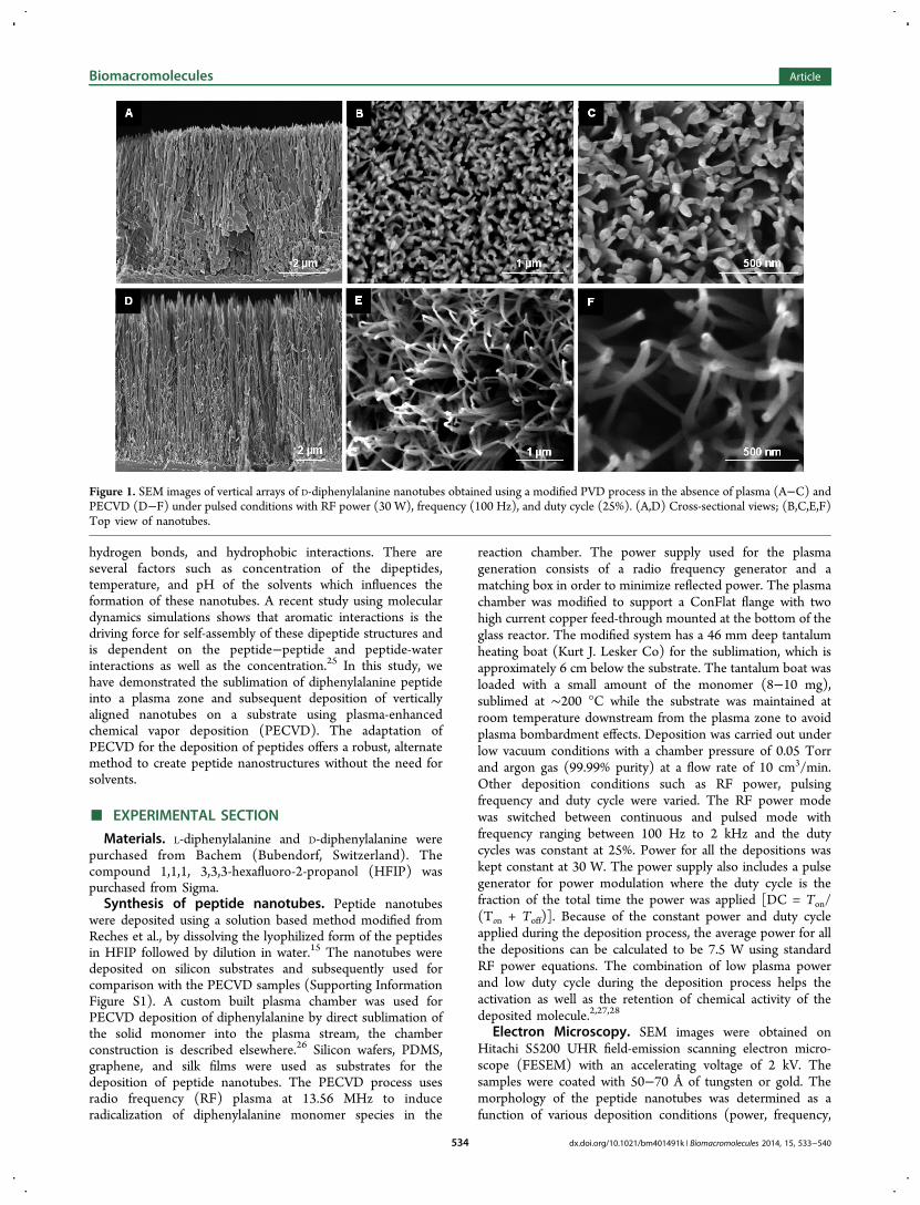
Figure 1. SEM images of vertical arrays of D-diphenylalanine nanotubes obtained using a modified PVD process in the absence of plasma (A−C) andPECVD (D−F) under pulsed conditions with RF power (30 W), frequency (100 Hz), and duty cycle (25%). (A,D) Cross-sectional views; (B,C,E,F)Top view of nanotubes.
Biomacromolecules Article
dx.doi.org/10.1021/bm401491k | Biomacromolecules 2014, 15, 533−540534

argon flow-rate, and deposition time) and both surface andcross-section images were obtained.Fourier-Transform Infrared (FTIR) and Circular Dichro-
ism (CD) Spectroscopy. Infrared spectra were obtained byusing a Nicolet Nexus 470 FTIR spectrometer fitted with ahelium neon laser and the transmission values were determinedusing the OMNIC program. Fourier self-deconvolution (FSD)of the infrared spectra in the amide I region was performedaccording to previously published procedures. Measurementswere made with 4 cm−1 resolution. CD measurements wereperformed to estimate the secondary structure using a JASCOJ-810 spectropolarimeter. The peptide nanotubes wereremoved from the silicon substrate by sonication in water. Aquartz cell of path length 1 mm was used in all themeasurements. Spectra were collected over the wavelengthrange 300−180 nm at 25 °C and background corrected using asolvent blank solution.X-ray Diffraction Measurements. Synchrotron X-ray
experiments were conducted at beamline 7.3.3 at the AdvancedLight Source at Livermore Berkeley National Laboratory at 10keV (1.24 Å) from a bend magnet and focused via a Mo/B4Cdouble multilayer monochromator. A Dectris Pilatus 1 Mdetector was used to collect 2D WAX patterns at sample-to-detector distances of 1.5 m. The 2D images were reduced usingthe Nika data reduction package for Igor Pro. The 1D WAXexperiments in in-plane and grazing geometry (out-of-plane)were carried out with a Rigaku Smartlab using CuKα radiation.Mechanical Property Measurements. The Nanoindenter
XP instrument by Agilent with a continuous stiffnessmeasurement (CSM) option was used in order to measurethe bulk Young’s modulus of the peptide arrays on a siliconsubstrate. A cylindrical flat-punch indenter (40 μm tip) wasused in the measurement of contact force. In situ SEMcompression was performed using a custom-built micro-mechanical test frame within an FEI Quanta ESEM.Compression utilized a 40 μm × 40 μm diamond flat punch.Displacement data was acquired using the National InstrumentsLabview program.29
■ RESULTS AND DISCUSSION
Vapor phase deposition of the peptide nanotubes canpotentially avoid the use of harsh chemicals such as HFIP,which is generally used for solvent-based synthesis of peptidenanotubes. The D-diphenylalanine monomer was heated toabout ∼200 °C and sublimed into the plasma stream. This
resulted in the deposition of conformal films on the substratesdownstream of the plasma. Observation of the deposited D-diphenylalanine films using SEM analysis indicated thepresence of large arrays of vertically aligned peptide nanotubeswith open ends at the nanotube tips (Figure 1). The depositednanotubes exhibited high aspect ratios with the length in therange of tens of micrometers and diameters of 50−300 nm.PECVD deposition of polymeric films of organic moleculessuch as D-diphenylalanine have a whole spectrum of chemicaland physical properties depending on the specific dischargeparameters used during the deposition process such as inputpower, chamber pressure, flow rate of the argon gas, andsubstrate position. The other main factor is the number andlifetime of the plasma species such as ions, radicals, andmetastables formed during the reaction. This particularly offersscope of compositional and microstructural tuning of thepolymeric films.4,30 The monomer, D-diphenylalanine uponsublimation in the tantalum boat rises into the plasma streamwhere the monomer undergoes ionization and free radicals arealso formed in the plasma. At the substrate surface, themonomer undergoes polymerization and forms a basal seedlayer from which the multibranched structures of nanotubesgrow. The use of pulsed plasma allows retention of the originalchemistry of the monomer and allows conventional polymer-ization to occur during the plasma “off” time and maybe moresuitable for biological monomers.2,4,7,9,30
For comparison, peptide nanotubes were also grown in amodified physical vapor deposition (PVD) process, bysublimation of diphenylalanine in the PECVD chamber in theabsence of the plasma.18 The nanostructures formed using PVDappear to be morphologically different when compared to thePECVD deposited nanostructures (Figure 1). The dipeptidearrays deposited by PVD appear less organized and the tips ofthe nanotubes are closed. In cross-sectional views (Figure 1D),the proximal ends of the PECVD deposited dipeptide nanotubearrays appear to be more homogeneous, while the PVDdeposited structures are discontinuous (Figure 1A). Higher-magnification images of the distal ends of the peptide arraysshow clear differences in the morphology of peptide nanotubes.The PECVD deposited D-diphenylalanine nanostructures havemore of a tube-like morphology compared to the PVD growndipeptide nanostructures (Figure 1F). The ends of the PECVDnanotubes are uniform and possess a high volume fraction ofopen tubes. The fibrils are usually hollow and sub-100 nm indiameter. Unlike physical vapor deposition (PVD), the
Figure 2. Cross-sectional SEM images of (A) proximal and (B−C) distal regions of vertical arrays of D-diphenylalanine nanostructures obtainedusing PECVD using pulsed conditions with RF power (30 W), frequency (100 Hz) and duty cycle (25%) indicating the bulk-surface heterogeneity.Dashed line denotes the interface between the silicon substrate and basal peptide seed layer. Scale bar is 500 nm for all images.
Biomacromolecules Article
dx.doi.org/10.1021/bm401491k | Biomacromolecules 2014, 15, 533−540535

morphology and density of the nanotubes can be controlled byvarying the PECVD conditions. The peptide nanotubesdeposited by PECVD show structural variation along its length.Closer examination of the proximal and distal ends of thepeptide arrays are shown in Figure 2. At the proximal end,peptide nanotube branches, originating from the basal seed
layer, form bundles composed of the individual nanotube fibers.
At the distal end, the bundles begin to flare out into fibrils,
narrowing to ∼50 nm in diameter. Both L- and D-isomers of
diphenylalanine, and other dipeptides such as dityrosine and
phenylalanine-tyrosine produced vertically aligned peptide
Figure 3. SEM images (top view) of D-diphenylalanine nanostructures grown under different deposition conditions with constant RF power of 30 Wand 25% duty cycle pulsed PECVD at (A) 250 Hz; (B) 500 Hz; (C) 750 Hz; and (D) continuous PECVD. Scale bar is 1 μm for all images.
Figure 4. Demonstration of the deposition of diphenylalanine nanotubes on various substrates. SEM images of PECVD-deposited diphenylalaninenanostructures on (A) carbon electrode; (B) graphene sheet; (C) PDMS; (D) PECVD grown nanotubes detached en bloc from the PDMSsubstrate. In all cases, PECVD pulsed conditions with RF power (30 W), frequency (100 Hz) and duty cycle (25%). Scale bar in images (A−C) is 1μm.
Biomacromolecules Article
dx.doi.org/10.1021/bm401491k | Biomacromolecules 2014, 15, 533−540536
nanostructures using PECVD (Supporting Information FigureS2).As mentioned earlier, the morphology and density of the
nanotubes can be easily controlled by varying the conditions forPECVD. Figure 3 shows the differences in morphologies in thediphenylalanine nanotubes grown on a silicon wafer undervarying deposition conditions starting with the continuousplasma to pulsed plasma depositions with constant duty cyclewith increasing frequency. Changing frequency or the pulseduration is the main contributor to the differing morphologies.These parameters control the degree of plasma ionization thatin turn influences the morphology and chemical composition ofthe deposited material. With changing frequency and dutycycle, we have observed changes in the gross morphology of thedeposited nanostructures from nanotubes to nanoribbon-likestructures. Average input power is controlled by changing thepeak power with a continuous wave discharge or by using apulsed wave discharge where the duty cycle dictates the amountof time that the peak power is applied. At higher frequencies,ribbon-like structures appear with larger widths at the higherfrequencies (Figure 3A−C). Unlike pulsed plasma deposition,the continuous plasma deposition resulted in disorderedstructures with a mixture of both ribbon-like and fibrillarstructures (Figure 3D). By controlling power, frequency andduty cycle, we were able to reproducibly deposit arrays of opentubular nanostructures with diameters of 50−100 nm at thedistal ends, while higher frequencies and duty cycles ribbon-likenanostructures were formed. Such morphological changes havenot been observed in the peptide nanotubes grown in solution-phase. The vertically aligned forests of D-diphenylalaninenanotubes showed RMS roughness on the order of 600 nmper 50 μm scan due to height discrepancies as measured on anAsylum MFP-3D AFM (Supporting Information Figure S3).Detached nanotubes grown via pulsed PECVD were depositedon a prefabricated electrode substrates and probed in theelectrostatic force measurement (EFM) mode on the AsylumMFP-3D AFM to demonstrate that the nanotubes had hollowinteriors31 (Supporting Information Figure S4). The peptidenanostructures produced by PECVD typically possess highaspect ratios, where the length of the nanotubes can be easilycontrolled by varying the PECVD deposition conditions andsurfaces coated with diphenylalanine nanotubes are hydro-phobic (Supporting Information Figure S5). The PECVDdeposited nanostructures were found to be at least twice thelength of the PVD deposited nanotubes grown for the sameduration of time.PECVD also allows for the formation of uniform and
homogeneous forests of nanotubes on a variety of substratesused in the deposition process. In Figure 4, SEM images of thediphenylalanine nanotubes obtained on the surface of carbonelectrode, graphene, and elastomer (PDMS) are shown. Theopen ended tubes can be clearly observed when a carbonelectrode substrate was used for deposition (Figure 4A). Thedipeptide nanotube arrays on graphene and PDMS appearedsimilar to each other but differed from the nanotubes on thecarbon electrode surface, exhibiting polygonal structures.Currently, we have no explanation for this observation, anddetailed studies of the effects of the growth process on thesubstrates will be needed to address this. Interestingly, theintact vertically aligned nanotube arrays can be easily detachedfrom the PDMS surface (Figure 4D). These examplesdemonstrate the ease of PECVD use for deposition on avariety of substrates.
The mechanism of self-assembly of the biomolecules inliquid environments has been studied in the past and involveshydrogen bonding and π−π stacking interactions but themechanism of peptide nanotube formation via vapor depositionhas not been established. The use of elevated temperatures inthe sublimation process may lead to thermally inducedchemical changes in the peptide structures. MALDI-TOFanalysis was used to verify that the diphenylalanine monomersundergo cyclization upon sublimation during the PECVDprocess (Supporting Information Figure S6). The cyclization ofdiphenylalanine has been seen in other methods used in theformation of diphenylalanine peptide nanotubes.18 We furthercharacterized these nanostructures using a variety of techniquesincluding FTIR, CD spectroscopy, and X-ray diffraction to gaininsight into the secondary structures formed by the PECVDdeposited dipeptides compared to PVD grown nanotubes. Asmentioned earlier, MALDI-TOF mass spectroscopy revealedcyclization of PECVD-deposited diphenylalanine, similar toobservations seen with HFIP or PVD grown nanotubes. FTIRanalysis of the diphenylalanine nanotubes gives us an insightinto their secondary structure. The PECVD grown peptidenanotubes show peaks in the amide I region (1650−1700 cm−1
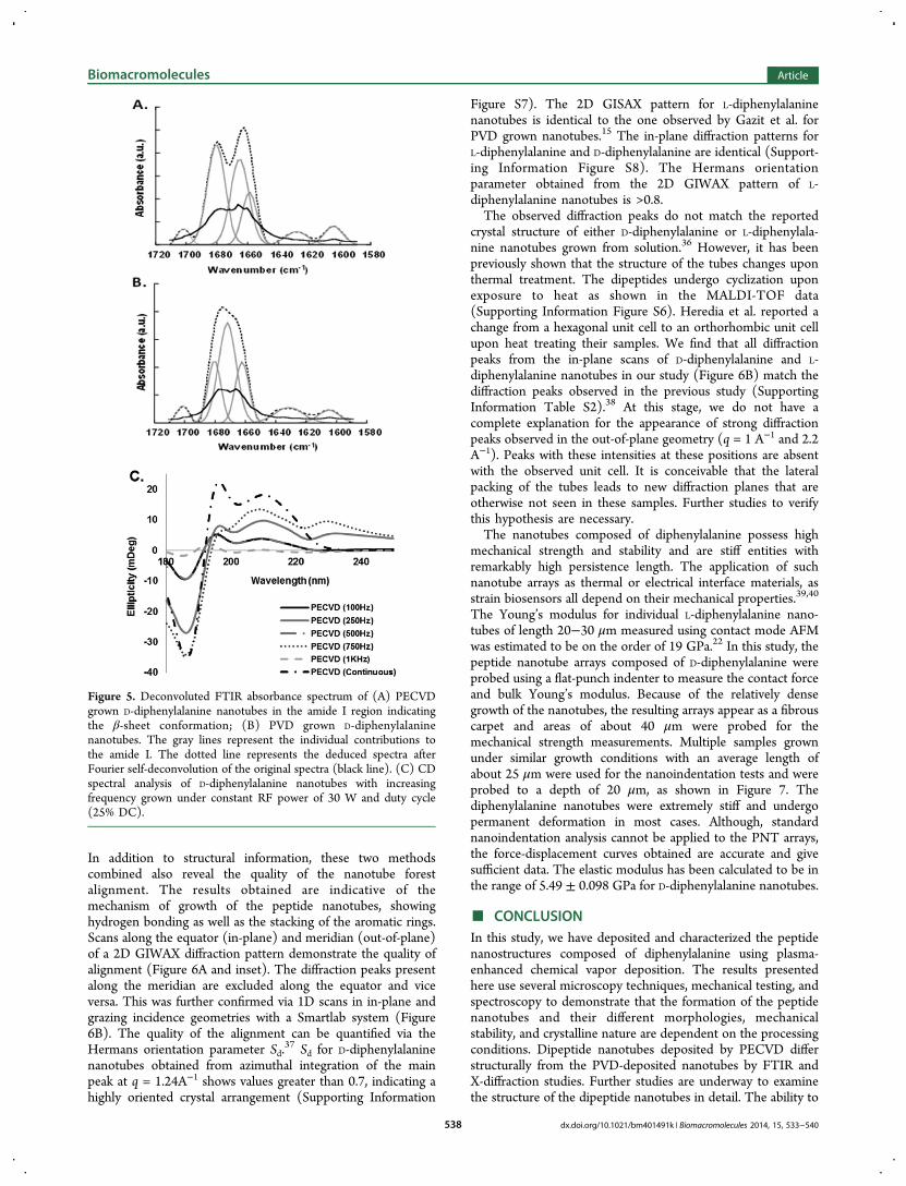
range), indicating β-sheet conformation.14,32 We used Fourierself-deconvolution of the infrared spectra in the amide I regionto evaluate the secondary component of the diphenylalaninenanotubes deposited using PVD or PECVD (Figure 5).33 Thestructural information based on the spectrum deconvolutionwithin the amide I region indicates an increase in the β-sheetcontent of PECVD deposited nanotubes when compared to thePVD (Supporting Information Table S1). This could beattributed to more ordered morphologies due to stacking of thearomatic rings and increased hydrogen bonding during thePECVD process compared to PVD process.CD spectral analysis was also used to study the secondary
structures of D-diphenylalanine nanotubes grown usingPECVD. The CD spectra of nanotubes obtained underconstant power and duty cycle conditions with varyingfrequencies from 100 Hz to 1 kHz are shown in Figure 5C.The CD spectra indicate the presence of well-pleated β-sheetstructures.34 The effect of the changing frequency on thequality of nanotubes is evident in the shown data, which wasfitted using the CDPro program, and the β-sheet content wasfound to be ∼55% in samples obtained at lower frequency.However, in peptide nanotubes deposited at higher frequencies(>750 Hz) the unordered structure content was found to behigher, approaching about 40%. This was also confirmedthrough the observation of macroscopic structures via SEM, thenanotubes appeared more disorder at higher frequencies.Though the peak power and duty cycle was constant for allthe depositions, the frequency of the pulse affected themorphology and characteristics of the deposited nanotubes.Previous studies on crystallization of single amino acids in
vapor phase showed that the crystal structures of the sublimateswas dependent on the hydrophobic or hydrophilic nature of theside chains.35 In particular, peptides with hydrophobic sidegroups such as valine and leucine have the identical crystalstructure when crystallization occurred either in solution or viasublimation. Conversely, peptides with hydrophilic side groupssuch as phenylalanine and tyrosine have significantly differentcrystal structures when crystallization occurred in aqueoussolutions as compared to sublimation.35,36 Wide-angle X-raydiffraction (WAX) studies were performed on the peptidenanotubes both in grazing and in-plane incidence geometries.
Biomacromolecules Article
dx.doi.org/10.1021/bm401491k | Biomacromolecules 2014, 15, 533−540537
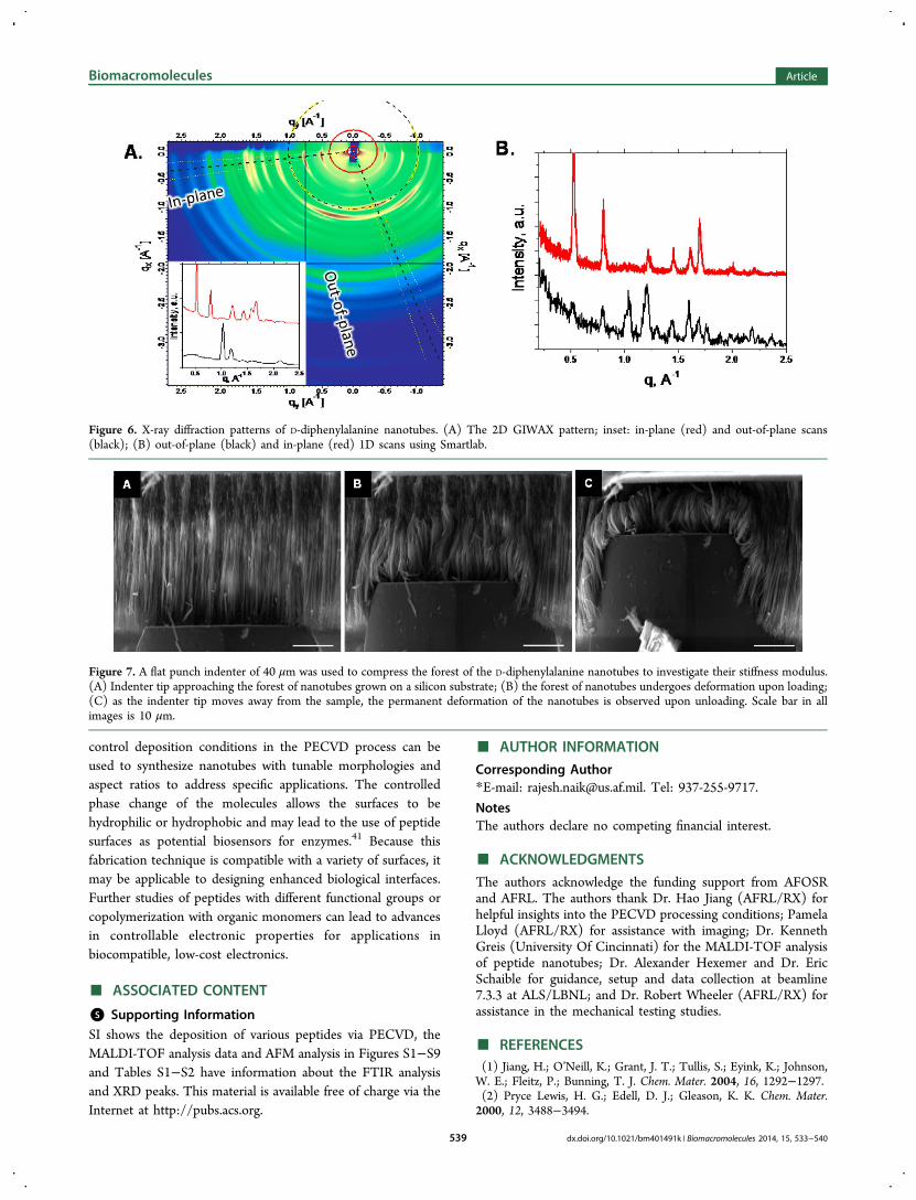
In addition to structural information, these two methodscombined also reveal the quality of the nanotube forestalignment. The results obtained are indicative of themechanism of growth of the peptide nanotubes, showinghydrogen bonding as well as the stacking of the aromatic rings.Scans along the equator (in-plane) and meridian (out-of-plane)of a 2D GIWAX diffraction pattern demonstrate the quality ofalignment (Figure 6A and inset). The diffraction peaks presentalong the meridian are excluded along the equator and viceversa. This was further confirmed via 1D scans in in-plane andgrazing incidence geometries with a Smartlab system (Figure6B). The quality of the alignment can be quantified via theHermans orientation parameter Sd.
37 Sd for D-diphenylalaninenanotubes obtained from azimuthal integration of the mainpeak at q = 1.24A−1 shows values greater than 0.7, indicating ahighly oriented crystal arrangement (Supporting Information
Figure S7). The 2D GISAX pattern for L-diphenylalaninenanotubes is identical to the one observed by Gazit et al. forPVD grown nanotubes.15 The in-plane diffraction patterns forL-diphenylalanine and D-diphenylalanine are identical (Support-ing Information Figure S8). The Hermans orientationparameter obtained from the 2D GIWAX pattern of L-diphenylalanine nanotubes is >0.8.The observed diffraction peaks do not match the reported
crystal structure of either D-diphenylalanine or L-diphenylala-nine nanotubes grown from solution.36 However, it has beenpreviously shown that the structure of the tubes changes uponthermal treatment. The dipeptides undergo cyclization uponexposure to heat as shown in the MALDI-TOF data(Supporting Information Figure S6). Heredia et al. reported achange from a hexagonal unit cell to an orthorhombic unit cellupon heat treating their samples. We find that all diffractionpeaks from the in-plane scans of D-diphenylalanine and L-diphenylalanine nanotubes in our study (Figure 6B) match thediffraction peaks observed in the previous study (SupportingInformation Table S2).38 At this stage, we do not have acomplete explanation for the appearance of strong diffractionpeaks observed in the out-of-plane geometry (q = 1 A−1 and 2.2A−1). Peaks with these intensities at these positions are absentwith the observed unit cell. It is conceivable that the lateralpacking of the tubes leads to new diffraction planes that areotherwise not seen in these samples. Further studies to verifythis hypothesis are necessary.The nanotubes composed of diphenylalanine possess high
mechanical strength and stability and are stiff entities withremarkably high persistence length. The application of suchnanotube arrays as thermal or electrical interface materials, asstrain biosensors all depend on their mechanical properties.39,40
The Young’s modulus for individual L-diphenylalanine nano-tubes of length 20−30 μm measured using contact mode AFMwas estimated to be on the order of 19 GPa.22 In this study, thepeptide nanotube arrays composed of D-diphenylalanine wereprobed using a flat-punch indenter to measure the contact forceand bulk Young’s modulus. Because of the relatively densegrowth of the nanotubes, the resulting arrays appear as a fibrouscarpet and areas of about 40 μm were probed for themechanical strength measurements. Multiple samples grownunder similar growth conditions with an average length ofabout 25 μm were used for the nanoindentation tests and wereprobed to a depth of 20 μm, as shown in Figure 7. Thediphenylalanine nanotubes were extremely stiff and undergopermanent deformation in most cases. Although, standardnanoindentation analysis cannot be applied to the PNT arrays,the force-displacement curves obtained are accurate and givesufficient data. The elastic modulus has been calculated to be inthe range of 5.49 ± 0.098 GPa for D-diphenylalanine nanotubes.
■ CONCLUSIONIn this study, we have deposited and characterized the peptidenanostructures composed of diphenylalanine using plasma-enhanced chemical vapor deposition. The results presentedhere use several microscopy techniques, mechanical testing, andspectroscopy to demonstrate that the formation of the peptidenanotubes and their different morphologies, mechanicalstability, and crystalline nature are dependent on the processingconditions. Dipeptide nanotubes deposited by PECVD differstructurally from the PVD-deposited nanotubes by FTIR andX-diffraction studies. Further studies are underway to examinethe structure of the dipeptide nanotubes in detail. The ability to
Figure 5. Deconvoluted FTIR absorbance spectrum of (A) PECVDgrown D-diphenylalanine nanotubes in the amide I region indicatingthe β-sheet conformation; (B) PVD grown D-diphenylalaninenanotubes. The gray lines represent the individual contributions tothe amide I. The dotted line represents the deduced spectra afterFourier self-deconvolution of the original spectra (black line). (C) CDspectral analysis of D-diphenylalanine nanotubes with increasingfrequency grown under constant RF power of 30 W and duty cycle(25% DC).
Biomacromolecules Article
dx.doi.org/10.1021/bm401491k | Biomacromolecules 2014, 15, 533−540538
control deposition conditions in the PECVD process can beused to synthesize nanotubes with tunable morphologies andaspect ratios to address specific applications. The controlledphase change of the molecules allows the surfaces to behydrophilic or hydrophobic and may lead to the use of peptidesurfaces as potential biosensors for enzymes.41 Because thisfabrication technique is compatible with a variety of surfaces, itmay be applicable to designing enhanced biological interfaces.Further studies of peptides with different functional groups orcopolymerization with organic monomers can lead to advancesin controllable electronic properties for applications inbiocompatible, low-cost electronics.
■ ASSOCIATED CONTENT
*S Supporting InformationSI shows the deposition of various peptides via PECVD, theMALDI-TOF analysis data and AFM analysis in Figures S1−S9and Tables S1−S2 have information about the FTIR analysisand XRD peaks. This material is available free of charge via theInternet at http://pubs.acs.org.
■ AUTHOR INFORMATION
Corresponding Author*E-mail: [email protected]. Tel: 937-255-9717.
NotesThe authors declare no competing financial interest.
■ ACKNOWLEDGMENTS
The authors acknowledge the funding support from AFOSRand AFRL. The authors thank Dr. Hao Jiang (AFRL/RX) forhelpful insights into the PECVD processing conditions; PamelaLloyd (AFRL/RX) for assistance with imaging; Dr. KennethGreis (University Of Cincinnati) for the MALDI-TOF analysisof peptide nanotubes; Dr. Alexander Hexemer and Dr. EricSchaible for guidance, setup and data collection at beamline7.3.3 at ALS/LBNL; and Dr. Robert Wheeler (AFRL/RX) forassistance in the mechanical testing studies.
■ REFERENCES(1) Jiang, H.; O’Neill, K.; Grant, J. T.; Tullis, S.; Eyink, K.; Johnson,W. E.; Fleitz, P.; Bunning, T. J. Chem. Mater. 2004, 16, 1292−1297.(2) Pryce Lewis, H. G.; Edell, D. J.; Gleason, K. K. Chem. Mater.2000, 12, 3488−3494.
Figure 6. X-ray diffraction patterns of D-diphenylalanine nanotubes. (A) The 2D GIWAX pattern; inset: in-plane (red) and out-of-plane scans(black); (B) out-of-plane (black) and in-plane (red) 1D scans using Smartlab.
Figure 7. A flat punch indenter of 40 μm was used to compress the forest of the D-diphenylalanine nanotubes to investigate their stiffness modulus.(A) Indenter tip approaching the forest of nanotubes grown on a silicon substrate; (B) the forest of nanotubes undergoes deformation upon loading;(C) as the indenter tip moves away from the sample, the permanent deformation of the nanotubes is observed upon unloading. Scale bar in allimages is 10 μm.
Biomacromolecules Article
dx.doi.org/10.1021/bm401491k | Biomacromolecules 2014, 15, 533−540539

(3) Yang, G.; Wang, X.; Xu, Q.; Wang, S.; Tian, H.; Zheng, W. J. SolidState Chem. 2009, 182, 966−972.(4) Friedrich, J. Plasma Processes Polym. 2011, 8, 783−802.(5) Hayakawa, T.; Yoshinari, M.; Nemoto, K. Biomaterials 2004, 25,119−127.(6) Lopes, B. B.; Davanzo, C. U.; Schreiner, W.; Durrant, S. F. Surf.Coat. Technol. 2008, 203, 526−529.(7) Jenkins, A. T. A.; Hu, J.; Wang, Y. Z.; Schiller, S.; Foerch, R.;Knoll, W. Langmuir 2000, 16, 6381−6384.(8) Jerome Perrin, J. S.; Hollenstein, Christoph; Howling, Alan;Sansonnens, Laurent Plasma Phys. Controlled Fusion 2000, 42, B353−B363.(9) Vasudev, M. C.; Anderson, K. D.; Bunning, T. J.; Tsukruk, V. V.;Naik, R. R. ACS Appl. Mater. Interfaces 2013, 5, 3983−3994.(10) Aparicio, F. J.; Borras, A.; Blaszczyk-Lezak, I.; Groning, P.;Alvarez-Herrero, A.; Fernandez-Rodríguez, M.; Gonzalez-Elipe, A. R.;Barranco, A. Plasma Processes Polym. 2009, 6, 17−26.(11) Sardella, E.; Favia, P.; Gristina, R.; Nardulli, M.; d’Agostino, R.Plasma Processes Polym. 2006, 3, 456−469.(12) Anderson, K. D.; Slocik, J. M.; McConney, M. E.; Enlow, J. O.;Jakubiak, R.; Bunning, T. J.; Naik, R. R.; Tsukruk, V. V. Small 2009, 5,741−749.(13) Anderson, K. D.; Young, S. L.; Jiang, H.; Jakubiak, R.; Bunning,T. J.; Naik, R. R.; Tsukruk, V. V. Langmuir 2012, 28, 1833−1845.(14) Reches, M.; Gazit, E. Science 2003, 300, 625−627.(15) Reches, M.; Gazit, E. Nat. Nanotechnol. 2006, 1, 195−200.(16) Song, Y.; Challa, S. R.; Medforth, C. J.; Qiu, Y.; Watt, R. K.;Pena, D.; Miller, J. E.; Swol, F. V.; Shelnutt, J. A. Chem. Commun.2004, 1044−1045.(17) Amdursky, N.; Molotskii, M.; Gazit, E.; Rosenman, G. J. Am.Chem. Soc. 2010, 132, 15632−15636.(18) Adler-Abramovich, L.; Aronov, D.; Beker, P.; Yevnin, M.;Stempler, S.; Buzhansky, L.; Rosenman, G.; Gazit, E. Nat. Nanotechnol.2009, 4, 849−854.(19) Ryu, J.; Park, C. B. Adv. Mater. 2008, 20, 3754−3758.(20) Ryu, J.; Park, C. B. Chem. Mater. 2008, 20, 4284−4290.(21) Adler-Abramovich, L.; Reches, M.; Sedman, V. L.; Allen, S.;Tendler, S. J. B.; Gazit, E. Langmuir 2006, 22, 1313−1320.(22) Kol, N.; Adler-Abramovich, L.; Barlam, D.; Shneck, R. Z.; Gazit,E.; Rousso, I. Nano Lett. 2005, 5, 1343−1346.(23) Sedman, V. L.; Adler-Abramovich, L.; Allen, S.; Gazit, E.;Tendler, S. J. B. J. Am. Chem. Soc. 2006, 128, 6903−6908.(24) Amdursky, N.; Molotskii, M.; Aronov, D.; Adler-Abramovich,L.; Gazit, E.; Rosenman, G. Nano Lett. 2009, 9, 3111−3115.(25) Guo, C.; Luo, Y.; Zhou, R.; Wei, G. ACS Nano 2012, 6, 3907−3918.(26) Enlow, J. O.; Jiang, H.; Grant, J. T.; Eyink, K.; Su, W.; Bunning,T. J. Polymer 2008, 49, 4042−4045.(27) Harsch, A.; Calderon, J.; Timmons, R. B.; Gross, G. W. J.Neurosci. Methods 2000, 98, 135−144.(28) Tarducci, C.; Schofield, W. C. E.; Badyal, J. P. S.; Brewer, S. A.;Willis, C. Chem. Mater. 2002, 14, 2541−2545.(29) Maschmann, M. R.; Zhang, Q.; Wheeler, R.; Du, F.; Dai, L.;Baur, J. ACS Appl. Mater. Interfaces 2011, 3, 648−653.(30) Yasuda, H.; Hsu, T. J. Polym. Sci., Polym. Chem. Ed. 1977, 15,81−97.(31) Clausen, C. H.; Jensen, J.; Castillo, J.; Dimaki, M.; Svendsen, W.E. Nano Lett. 2008, 8, 4066−4069.(32) Ryu, J.; Park, C. B. Angew. Chem., Int. Ed. 2009, 48, 4820−4823.(33) Haris, P. I.; Chapman, D. Biopolymers 1995, 37, 251−263.(34) Greenfield, N. J. Nat. Protoc. 2007, 1, 2876−2890.(35) Liu, Z.; Li, C. Biophys. Chem. 2008, 138, 115−119.(36) Gorbitz, C. H. Chem. Commun. 2006, 2332−2334.(37) Alexander, L. E. X-Ray Diffraction Methods in Polymer Science;Robert, E. Krieger publishing Company, 1979.(38) Heredia, A.; Bdikin, I.; Kopyl, S.; Mishina, E.; Semin, S.; Sigov,A.; German, K.; Bystrov, V.; Gracio, J.; Kholkin, A. L. J. Phys. D: Appl.Phys. 2010, 43, 462001.(39) Beker, P.; Rosenman, G. J. Mater. Res. 2010, 25, 1661−1666.
(40) Sopher, N. B.; Abrams, Z. R.; Reches, M.; Gazit, E.; Hanein, Y. J.Micromech. Microeng. 2007, 17, 2360.(41) Yemini, M.; Reches, M.; Gazit, E.; Rishpon, J. Anal. Chem. 2005,77, 5155−5159.
Biomacromolecules Article
dx.doi.org/10.1021/bm401491k | Biomacromolecules 2014, 15, 533−540540