Embed Size (px)
Citation preview

Venture Business LaboratoryTohoku University
Development of Sensors and Micromachines(Micro Nano-Machining)
Dec. 2000

Objectives of VBL in Tohoku University
Major research flelds in VBL1) Sensors and micromachines with micro- and nano- machining
VBL in Tohoku University was established by the fund for creative research projects in the 1995 fiscal year supplementary budget of Japanese Government. The responsibilities for research and development in VBL are shared amongst all the faculties of Tohoku University. The faculty of Engineering maintains the prime responsibility for the VBL. VBL's primary mission is educational and to provide the facilities and working environment that makes possible graduate education through research m the area of "Sensor and Mrcromachine technologres" (Micro- and Nano-Machining) and "Integrated Microsystem technologies". The objectives of the VBL are epitomized in the three major roles of the laboratory as stated below. 1) Promoting creative research and practical development that generate new business. 2) Bringing up of creative person who has advanced professional ability and venture spirit. 3) Providing graduate school with facilities for education and research including large-sized special equipment. For the above purposes, a new building for "sensor and micromachine" and "integrated microsystems" has been constructed in Aoba-yama campus in addition to improving and rearranging the existing micromachining facilities. The building includes LSI fabrication facilities. We push forward with new idea from young researchers, especially graduate school students, and train the student until he has a wide variety of professional ability through interdisciplinary cooperation of the individual departments and graduate schools. The cooperative research projects accepting researchers from industries, universities and governments are promoted actively. International exchange through the fellowships for foreign scientists and dispatch of young scientists for research abroad are performed actively. The scientific and technological results obtained from the VBL will be distributed worldwide.
Living creature has high-level functions since it is composed of many kinds of molecular parts. Similarly, micro-electro-mechanical system in which many different functional elements are integrated can be produced by the "micromachining" technology. The micromachining technology developed from the fabrication technologies for the semiconductor integrated circuits, and fused with those in optics, electronics, mechanical engineering, material sciences etc. Using the micromachining technology, high-level functional sensors and micromachines can be produced in a tiny space and many different elements are integrated. Micromachining is a key technology to develop novel microsystems; flexible machine with actuators, sensors and signal processing circuits distributed in it, instrumentation system with the sensitivity superior to conventional measurement limit, advanced interface elements necessary for information processing. On the other hand, similarly to the living creatures self-organized by the interaction between molecules, ultra-fine structures can be generated by manipulating atoms and molecules with nanomachining technology. Ultra-fine structure is a key technology to make breakthrough. As stated above, the mission of the VBL in Tohoku University is to develop "sensors and micromachines" utilizing micro- and nano-machining and to generate a new venture business. Fusing miniaturization and integration technologies with a variety of novel technologies, several microsystems will be possible in the wide areas covering from computer peripherals and medical instruments to space applications.
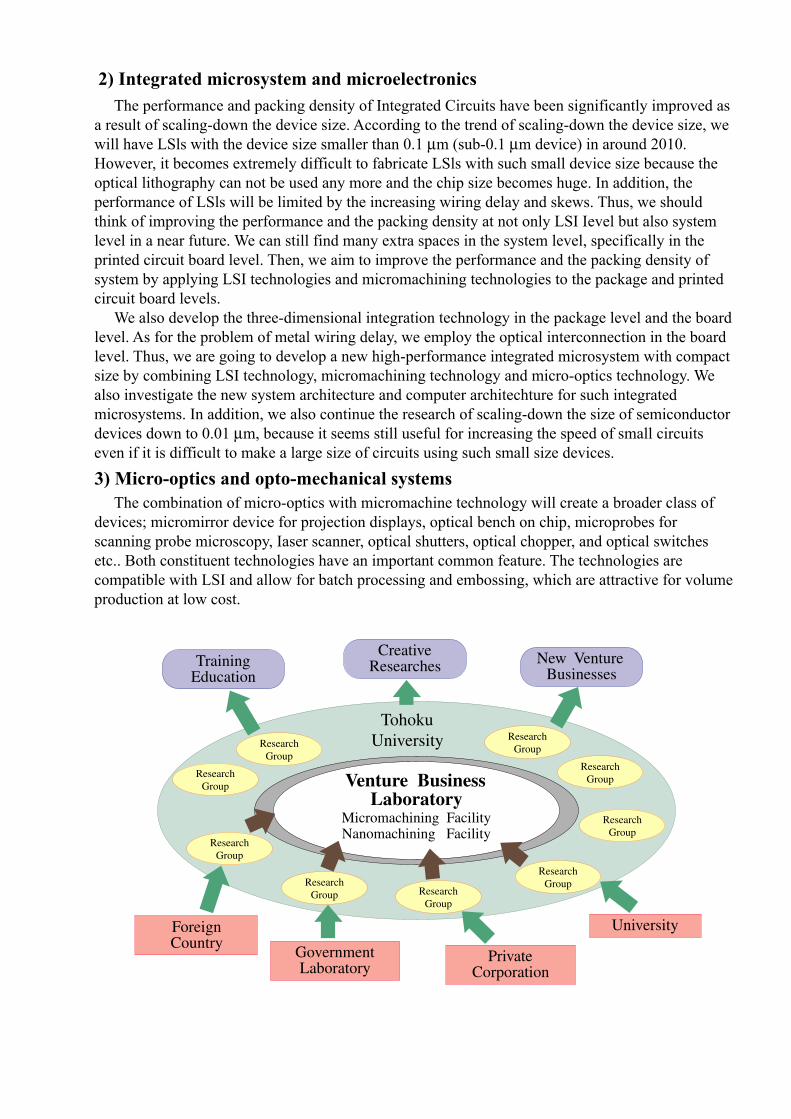
2) Integrated microsystem and microelectronics The performance and packing density of Integrated Circuits have been significantly improved as a result of scaling-down the device size. According to the trend of scaling-down the device size, we will have LSls with the device size smaller than 0.1 µm (sub-0.1 µm device) in around 2010. However, it becomes extremely difficult to fabricate LSls with such small device size because the optical lithography can not be used any more and the chip size becomes huge. In addition, the performance of LSls will be limited by the increasing wiring delay and skews. Thus, we should think of improving the performance and the packing density at not only LSI Ievel but also system level in a near future. We can still find many extra spaces in the system level, specifically in the printed circuit board level. Then, we aim to improve the performance and the packing density of system by applying LSI technologies and micromachining technologies to the package and printed circuit board levels. We also develop the three-dimensional integration technology in the package level and the board level. As for the problem of metal wiring delay, we employ the optical interconnection in the board level. Thus, we are going to develop a new high-performance integrated microsystem with compact size by combining LSI technology, micromachining technology and micro-optics technology. We also investigate the new system architecture and computer architechture for such integrated microsystems. In addition, we also continue the research of scaling-down the size of semiconductor devices down to 0.01 µm, because it seems still useful for increasing the speed of small circuits even if it is difficult to make a large size of circuits using such small size devices.
3) Micro-optics and opto-mechanical systems The combination of micro-optics with micromachine technology will create a broader class of devices; micromirror device for projection displays, optical bench on chip, microprobes for scanning probe microscopy, Iaser scanner, optical shutters, optical chopper, and optical switches etc.. Both constituent technologies have an important common feature. The technologies are compatible with LSI and allow for batch processing and embossing, which are attractive for volume production at low cost.
ResearchGroup
ResearchGroup
ResearchGroup
ResearchGroup
ResearchGroup
ResearchGroup
ResearchGroup
ResearchGroup
ResearchGroup
TrainingEducation
ForeignCountry
GovernmentLaboratory
PrivateCorporation
University
CreativeResearches New Venture
Businesses
Venture BusinessLaboratory
Micromachining FacilityNanomachining Facility
TohokuUniversity
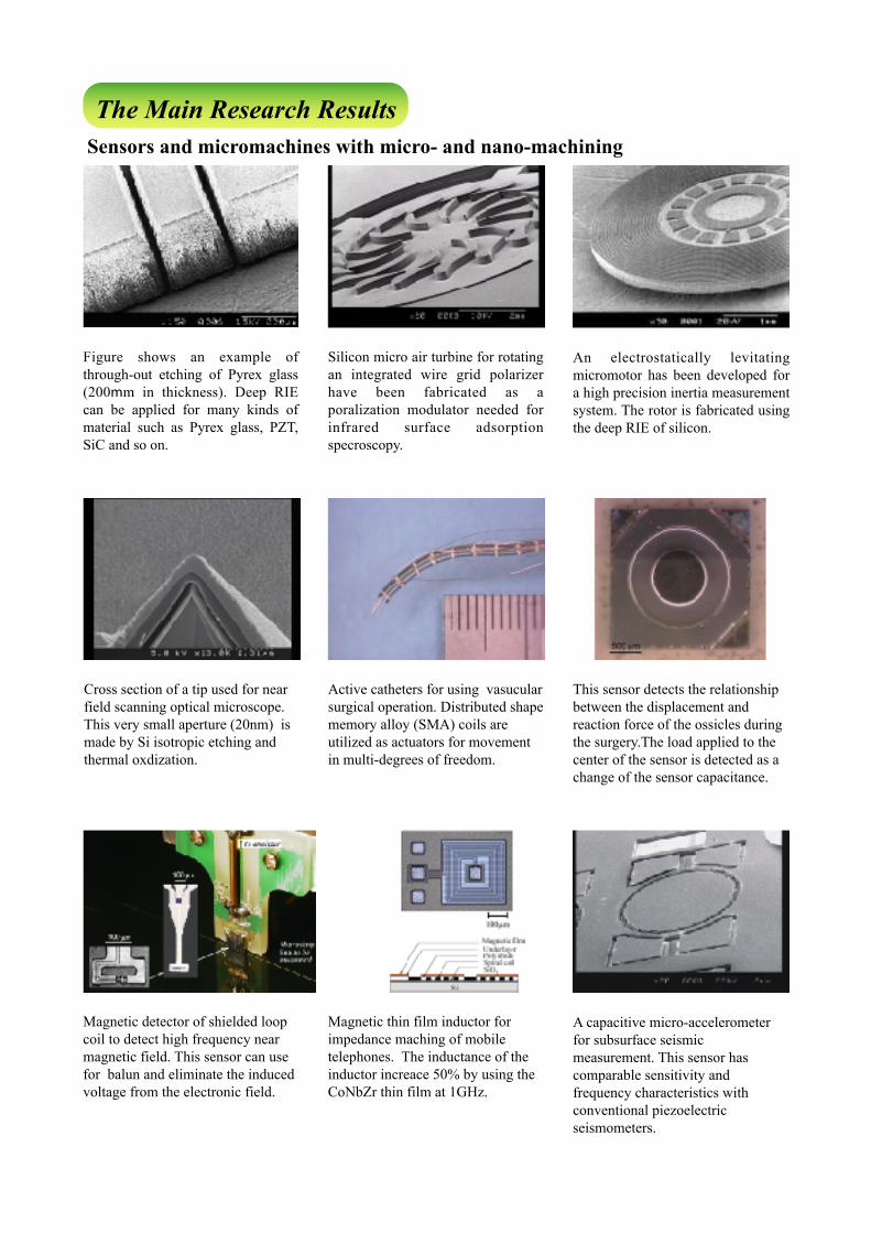
Sensors and micromachines with micro- and nano-machining
Figure shows an example of through-out etching of Pyrex glass (200mm in thickness). Deep RIE can be applied for many kinds of material such as Pyrex glass, PZT, SiC and so on.
An electrostatically levitating micromotor has been developed for a high precision inertia measurement system. The rotor is fabricated using the deep RIE of silicon.
Magnetic detector of shielded loop coil to detect high frequency near magnetic field. This sensor can use for balun and eliminate the induced voltage from the electronic field.
Magnetic thin film inductor for impedance maching of mobile telephones. The inductance of the inductor increace 50% by using the CoNbZr thin film at 1GHz.
Silicon micro air turbine for rotating an integrated wire grid polarizer have been fabricated as a poralization modulator needed for infrared surface adsorption specroscopy.
The Main Research Results
Active catheters for using vasucular surgical operation. Distributed shape memory alloy (SMA) coils are utilized as actuators for movement in multi-degrees of freedom.
Cross section of a tip used for near field scanning optical microscope. This very small aperture (20nm) is made by Si isotropic etching and thermal oxdization.
A capacitive micro-accelerometer for subsurface seismic measurement. This sensor has comparable sensitivity and frequency characteristics with conventional piezoelectric seismometers.
This sensor detects the relationship between the displacement and reaction force of the ossicles during the surgery.The load applied to the center of the sensor is detected as a change of the sensor capacitance.
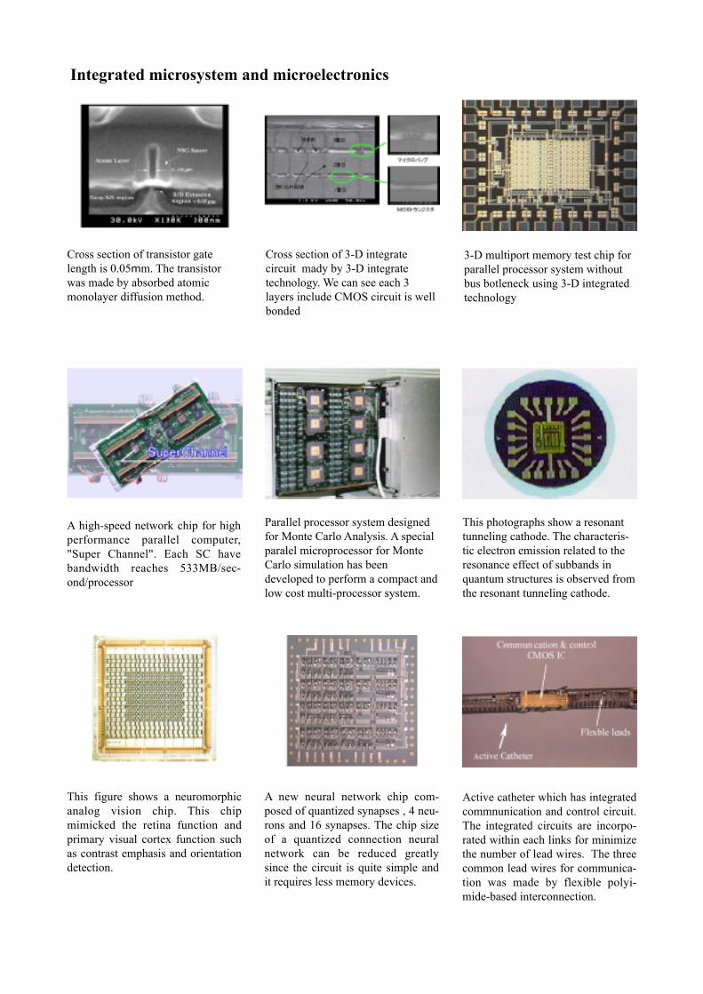
Parallel processor system designed for Monte Carlo Analysis. A special paralel microprocessor for Monte Carlo simulation has been developed to perform a compact and low cost multi-processor system.
A high-speed network chip for high performance parallel computer, "Super Channel". Each SC have bandwidth reaches 533MB/sec-ond/processor
3-D multiport memory test chip for parallel processor system without bus botleneck using 3-D integrated technology
This figure shows a neuromorphic analog vision chip. This chip mimicked the retina function and primary visual cortex function such as contrast emphasis and orientation detection.
Cross section of 3-D integrate circuit mady by 3-D integrate technology. We can see each 3 layers include CMOS circuit is well bonded
This photographs show a resonant tunneling cathode. The characteris-tic electron emission related to the resonance effect of subbands in quantum structures is observed from the resonant tunneling cathode.
Integrated microsystem and microelectronics
Active catheter which has integrated commnunication and control circuit. The integrated circuits are incorpo-rated within each links for minimize the number of lead wires. The three common lead wires for communica-tion was made by flexible polyi-mide-based interconnection.
A new neural network chip com-posed of quantized synapses , 4 neu-rons and 16 synapses. The chip size of a quantized connection neural network can be reduced greatly since the circuit is quite simple and it requires less memory devices.
Cross section of transistor gate length is 0.05mm. The transistor was made by absorbed atomic monolayer diffusion method.
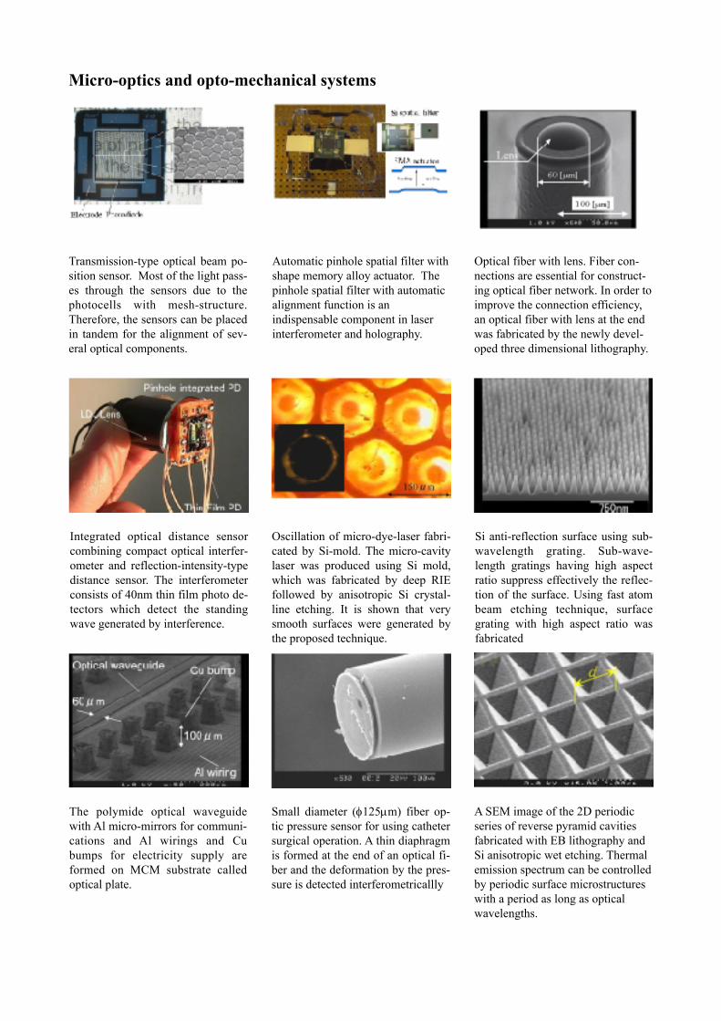
Automatic pinhole spatial filter with shape memory alloy actuator. The pinhole spatial filter with automatic alignment function is an indispensable component in laser interferometer and holography.
Optical fiber with lens. Fiber con-nections are essential for construct-ing optical fiber network. In order to improve the connection efficiency, an optical fiber with lens at the end was fabricated by the newly devel-oped three dimensional lithography.
Integrated optical distance sensor combining compact optical interfer-ometer and reflection-intensity-type distance sensor. The interferometer consists of 40nm thin film photo de-tectors which detect the standing wave generated by interference.
Oscillation of micro-dye-laser fabri-cated by Si-mold. The micro-cavity laser was produced using Si mold, which was fabricated by deep RIE followed by anisotropic Si crystal-line etching. It is shown that very smooth surfaces were generated by the proposed technique.
Si anti-reflection surface using sub-wavelength grating. Sub-wave-length gratings having high aspect ratio suppress effectively the reflec-tion of the surface. Using fast atom beam etching technique, surface grating with high aspect ratio was fabricated
A SEM image of the 2D periodic series of reverse pyramid cavities fabricated with EB lithography and Si anisotropic wet etching. Thermal emission spectrum can be controlled by periodic surface microstructures with a period as long as optical wavelengths.
The polymide optical waveguide with Al micro-mirrors for communi-cations and Al wirings and Cu bumps for electricity supply are formed on MCM substrate called optical plate.
Micro-optics and opto-mechanical systems
Small diameter (φ125µm) fiber op-tic pressure sensor for using catheter surgical operation. A thin diaphragm is formed at the end of an optical fi-ber and the deformation by the pres-sure is detected interferometricallly
Transmission-type optical beam po-sition sensor. Most of the light pass-es through the sensors due to the photocells with mesh-structure. Therefore, the sensors can be placed in tandem for the alignment of sev-eral optical components.
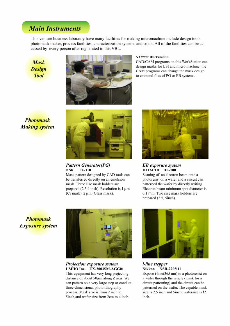
SX9000 WorkstationCAD/CAM programs on this WorkStation can design masks for LSI and micro machine. the CAM programs can change the mask design to cmmand files of PG or EB systems.
Projection exposure systemUSHIO Inc. UX-2003SM-AGG01This equipment has very long projecting distance of about 50µm along Z axis. We can pattern on a very large step or conduct three-dimensional photolithography process. Mask size is from 2 inch to 5inch,and wafer size from 2cm to 4 inch.
EB exposure systemHITACHI HL-700Scaning of an electron beam onto a photoresist on a wafer and a circuit can patterned the wafer by directly writing. Electron beam minimum spot diameter is 0.1 mm. Two size mask holders are prepared (2.5, 5inch).
i-line stepperNikkon NSR-2205i11Expose i-line(365 nm) to a photoresist on a wafer through the reticle (mask for a circuit patterning) and the circuit can be patterned on the wafer. The capable mask size is 2.5 inch and 5inch, wafersize is f2 inch.
Main InstrumentsThis venture business laboratoy have many facilities for making micromachine include design tools photomask maker, process facilities, characterization systems and so on. All of the facilities can be ac-cessed by every person after registrated to this VBL.
MaskDesign
Tool
PhotomaskMaking system
Photomask Exposure system
Pattern Generator(PG)NSK TZ-310Mask pattern designed by CAD tools can be transferred directly on an emulsion mask. Three size mask holders are prepared (2,3,4 inch). Resolution is 1 µm (Cr mask), 2 µm (Glass mask).
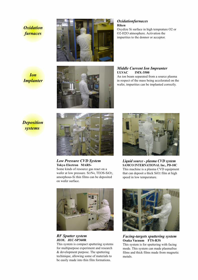
Low Pressure CVD SystemTokyo Electron MARS-ⅡSome kinds of resource gas react on a wafer at low pressure. Si3N4, TEOS-SiO2, amorphous-Si thin films can be deposited on wafer surface.
RF Sputter systemJEOL JEC-SP360R This system is compact sputtering systems for multipurpose experiment and research & development purpose. The sputtering techinique, allowing some of materials to be easily made into thin film formations.
Facing-targets sputtering systemOsaka Vacuum FTS-R3S This system is for sputtering with facing mode. This system can made plasmafree films and thick films made from magnetic metals.
Depositionsystems
Oxidation furnaces
IonImplanter
OxidationfurnacesRikenOxydize Si surface in high temprature O2 or O2-H2O atmosphere. Activation the impurities to the donnor or acceptor.
Middle Current Ion ImpranterULVAC IMX-3500An ion beam separated from a source plasma in respect of the mass being accelerated on the wafer, impurities can be implanted correctly.
Liquid source - plasma CVD systemSAMCO INTERNATIONAL Inc., PD-10CThis machine is a plasma CVD equipment that can deposit a thick SiO2 film at high speed in low temperature.
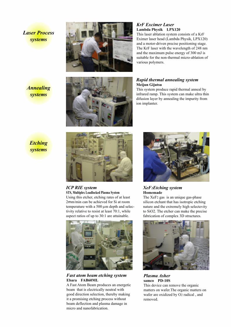
KrF Excimer LaserLambda Physik LPX120This laser ablation system consists of a KrF Eximer laser head (Lambda Physik, LPX120) and a motor-driven precise positioning stage. The KrF laser with the wavelength of 248 nm and the maximum pulse energy of 300 mJ is suitable for the non-thermal micro-ablation of various polymers.
Fast atom beam etching systemEbara FAB60MLA Fast Atom Beam produces an energetic beam that is electrically neutral with good direction selection, thereby making it a promising etching process without beam deflection and plasma damage in micro and nanofabrication.
Laser Process systems
Etchingsystems
Plasma Ashersamco PD-10SThis device can remove the organic matters on wafer.The organic matters on wafer are oxidized by O2 radical , and removed.
XeF2Etching systemHomemadeThe XeF2 gas is an unique gas-phase silicon etchant that has isotropic etching nature and the extremely high selectevity to SiO2. The etcher can make the precise fabrication of complex 3D structures.
Annealing systems
Rapid thermal annealing systemMeijun GijutsuThis system produce rapid thermal anneal by infrared ramp. This system can make ultra thin difusion layer by annealing the impurity from ion implanter.
ICP RIE systemSTS, Multiplex Loadlocked Plasma SystemUsing this etcher, etching rates of at least 2mm/min can be achieved for Si at room temperature with a 500 µm depth and selec-tivity relative to resist at least 70:1, while aspect ratios of up to 30:1 are attainable.
Analysissystem
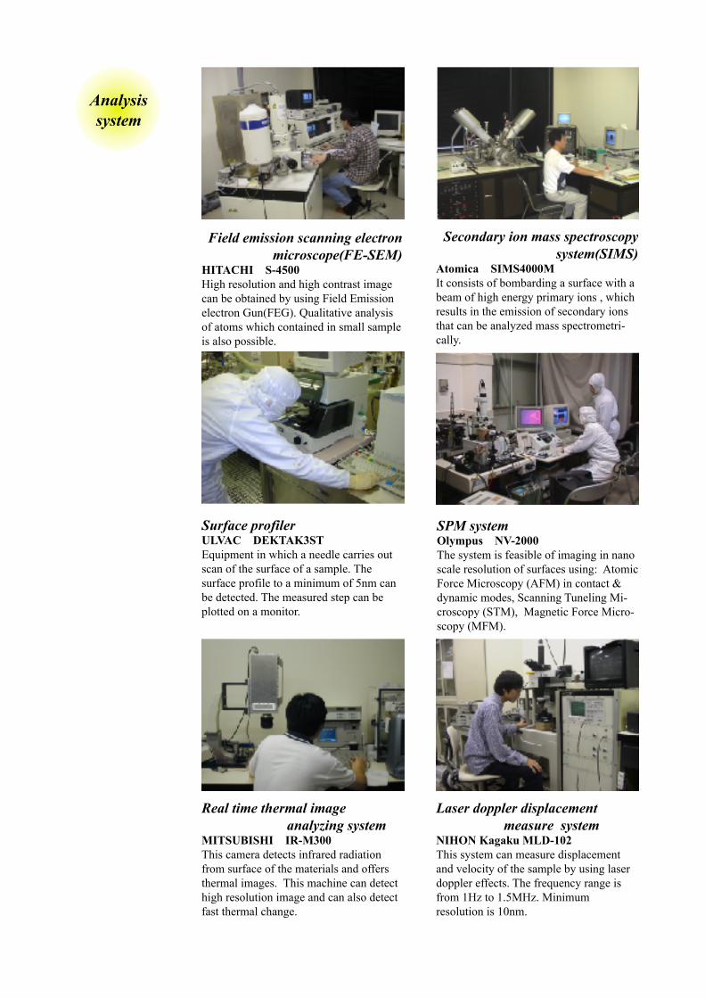
Real time thermal image analyzing systemMITSUBISHI IR-M300This camera detects infrared radiation from surface of the materials and offers thermal images. This machine can detect high resolution image and can also detect fast thermal change.
Laser doppler displacement measure systemNIHON Kagaku MLD-102This system can measure displacement and velocity of the sample by using laser doppler effects. The frequency range is from 1Hz to 1.5MHz. Minimum resolution is 10nm.
Field emission scanning electron microscope(FE-SEM)
HITACHI S-4500High resolution and high contrast image can be obtained by using Field Emission electron Gun(FEG). Qualitative analysis of atoms which contained in small sample is also possible.
Secondary ion mass spectroscopy system(SIMS)
Atomica SIMS4000MIt consists of bombarding a surface with a beam of high energy primary ions , which results in the emission of secondary ions that can be analyzed mass spectrometri-cally.
Surface profilerULVAC DEKTAK3STEquipment in which a needle carries out scan of the surface of a sample. The surface profile to a minimum of 5nm can be detected. The measured step can be plotted on a monitor.
SPM systemOlympus NV-2000 The system is feasible of imaging in nano scale resolution of surfaces using: Atomic Force Microscopy (AFM) in contact & dynamic modes, Scanning Tuneling Mi-croscopy (STM), Magnetic Force Micro-scopy (MFM).

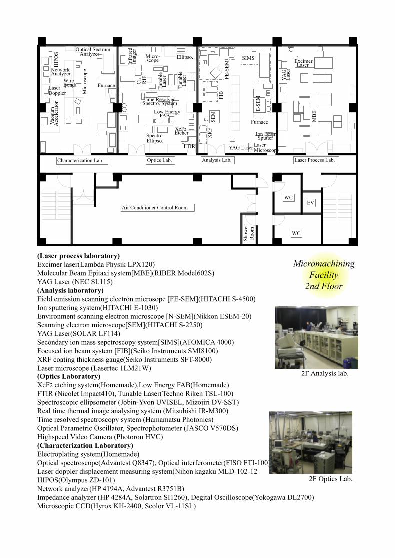
UHV STM AFM(JEOL JSTM4500)ECR-CVD system(Homemade)ESCA system (PHI 50C,Physical Electronics 1600CS)Atopospheric scanning probe microscope (Olympus NV-2000、Shimazu SPM-9500)Stepper/pattern generator(NSK TZ-310)VIM camera(HamamatsuPhotonics C2400-25)Reduction camera(Homemade), Photo repeater(Homemade)E-beam direct exposure system[EB] (Elionix ELS-3700S、 ELS-3300)Laser exposure system(Nippon Kagaku)Exposure system(ElectroVision EV-530)Anodic bonding system(ElectroVision EV-520)Projection exposure system(USHIO Inc. UX-2003SM-AGG01)CVD system for carbon nano tube(Homemade)
NanomachiningFacility
In the Yellow room
UHV-STM/AFM
Facilities and instruments The new "micromachining" building has three floors and the total floor space is 2,000m2. On the first floor, there is a down-flow type clean room of the 600m2 floor space. The half-micron CMOS base line and the fabrication line for sensors and micromachines are established in this clean room. Several laboratory rooms for the chemical and physical analyses and optical measurements are set up on the second floor. On the third floor, rooms for seminar, for visiting researchers and graduate students and for mini-museum of sensors, micromachines, microsystems and LSls are located. The Micromachining building in VBL contains LSI fabrication facilities including ultra-high vacuum CVD system. In addition, following facilities are equipped; the micromachining facility including anodic bonding system, the plasma CVD for the deposition of thick film, the facility for analysis including field emission electron microscopy, monitoring instruments such as time resolved laser spectroscopy system, spectroscopic ellipsometry in infrared, visible and ultraviolet regions. The "nanomachining" building which has already built nearby the micromachinig building, is a clean room of 150m2. Studies on surface sciences using ultra-high vacuum scanning tunneling microscopy and several kinds of surface analyzers can be carried out under the experimental conditions free from environmental vibration.
Stepper/PG
EBExposure
Atomos.AFM/STM
EB E
xpos
ure
ECR
CV
D
VIM
Red
uctio
nca
mer
a
Table
Photorepeater
Dark Room
UH
VST
M/A
FM
Laser exposuresystem
Carbon CVD
proj
ectio
n ex
posu
re
Anodic Bonder

EB exposure system(Hitachi HL-700, JEOL JBX-5000SM)I-line stepper(Nikkon NSR-2205i11)Spinner(Mikasa IH-DX), Furnace(Tchnofine TL400,AT-S30)Oxidation furnaces(Rikken, Kokusai Electronics)Ion implanter (ULVAC µP-150)UHV CVD system [UHV-CVD](ULVAC BC3217)Plasma CVD system[PECVD](Anelva PED-401, Samco PD-10C)Low-pressure CVD system[LPCVD](Tokyo electron MODEL2400)Atomospheric-pressure CVD system[APCVD](Chemitronics C-1100)Tungsten CVD system[W-CVD](ULVAC BC4969)Plasma Asher(Samco PD-10S)Chemical dry etcher[CDE](Mori engineering ASA-010)ECR etching system[ECR-RIE](ULVAC ECRE-200, Dainichi TH9107B)ICP-Reactive ion etching system(STS)Reactive ion etching system [RIE](Anelva L-2010D-L,L-201-D-L, Eiko ERI-10L)Fast atom beam etching system[FAB](Ebara FAB60ML)Multi-targets sputtering system(Anelva SPC-35, JEOL JEC-SP360R, Eiko ES-350)Radio-frequency sputtering system(Anelva SPF-210H, ULVAC MPS-2000-HC3)Laser Ablated sputtering system(ULVAC L-PVD-HC, Lambda physik LPX-205ICC)Facing-targets sputtering system(Osaka Vacuum FTS-R3S)Ion sputtering system(Nisshin Denki IVDS-800-SA) Vacuum deposition system(Tokuda CU-6ST-40)E-veam vacuum deposition system (Anelva VI-43N)Rapid thermal annealing system(Meijun Gijutsu)3-D Wafer alinger(Mitsubishi Heavy Industries)Surface profiler(ULVAC DEKTAK3ST)Ellipsometer(NipponKagaku EL-680W)
Micromachining Facility
1st Floor
Oxi
dat
ion
furn
aces
Oxi
dat
ion
furn
aces
UH
VC
VD
Pho
s. Dif
fu
I-linestepper
Microscope
Ionimplanter
RIE
CD
E
SpinnerFurnace
EB
Mic
rosc
op
e
Asher
RTAFAB
Ellip
so.
Vacuumdepo.
Clean wear dressing room
RFSputter
Facing targetssputter
MetalEtcher
PEC
VD
APCVD
Excimer Laser Lase
rA
blat
ion
Multi-targetssputter
EB Vacuumdepo.
RF sputter(Al)RF sputter
(Multi-targets)
ECR
LPC
VD
P-C
VD
RIEECR
STSIon Beam Sputter
STS
RF sputter(Multi-targets)
Profiler
W-CVD
3 dimensionalWafer bonder
EB
(Laser process laboratory)Excimer laser(Lambda Physik LPX120)Molecular Beam Epitaxi system[MBE](RIBER Model602S)YAG Laser (NEC SL115)(Analysis laboratory)Field emission scanning electron microsope [FE-SEM](HITACHI S-4500)Ion sputtering system(HITACHI E-1030)Environment scanning electron microscope [N-SEM](Nikkon ESEM-20)Scanning electron microscope[SEM](HITACHI S-2250)YAG Laser(SOLAR LF114)Secondary ion mass sepctroscopy system[SIMS](ATOMICA 4000)Focused ion beam system [FIB](Seiko Instruments SMI8100)XRF coating thickness gauge(Seiko Instruments SFT-8000)Laser microscope (Lasertec 1LM21W)(Optics Laboratory)XeF2 etching system(Homemade),Low Energy FAB(Homemade)FTIR (Nicolet Impact410), Tunable Laser(Techno Riken TSL-100)Spectroscopic ellipsometer (Jobin-Yvon UVISEL, Mizojiri DV-SST)Real time thermal image analysing system (Mitsubishi IR-M300)Time resolved spectroscopy system (Hamamatsu Photonics)Optical Parametric Oscillator, Spectrophotometer (JASCO V570DS)Highspeed Video Camera (Photoron HVC)(Characterization Laboratory)Electroplating system(Homemade)Optical spectroscope(Advantest Q8347), Optical interferometer(FISO FTI-100)Laser doppler displacement measuring system(Nihon kagaku MLD-102-12HIPOS(Olympus ZD-101)Network analyzer(HP 4194A, Advantest R3751B)Impedance analyzer (HP 4284A, Solartron SI1260), Degital Oscilloscope(Yokogawa DL2700)Microscopic CCD(Hyrox KH-2400, Scolor VL-11SL)
2F Analysis lab.
2F Optics Lab.
Micromachining Facility
2nd Floor
(Ehibition hall)Mini-museum for sensors and micromachines(Computer room)ULSI design tools (SEIKO SX-9000)FEM simulation tools(ANSYS)(Electronic workshop)Electronic parts
2F Laser process Lab.2F Characterization Lab.
3F ehibition hall
3F Computer room
1F Cleanroom 1F Cleanroom 1F Metal evaporate room
Micromachining Facility
3rd Floor
Please inform the matter to the appointed person. In case of shortage of the consumption, the announcement prefer to the shortage is desired to avoid the trouble related to the shortage (ex. targets). In case of trouble of the equipment, the users must work and act together under the direction of the person responsible for the equipment. The maintenance, repaire and instructions are done volatility. The users are required to know their responsibility for the repaire of the equipment, together with the person responsible for the equipment.
VBL FAQQ Is there any fequirement on qualification of users to utilize the equipments inVBL ?
About 50 laboratories are now utilizing the facility. Each laboratory within Tohoku University uses the facility freely after the procedures given below. At first, the laboratory is required to choose representative for using the VBL. In case of visiting researcher from outside of the university, the authorized person in direct contact with them maintains prime responsibility for using the VBL. You can ask the details at a joint research laboratory located in the 3 rd floor of VBL.
Q Could you tell me how to use the equipment ? You can ask any questions to the person responsible for the operation of the equipment. The appointed person is selected from the users who use the equipment most frequently. The operation of the equipment is performed under the direction and instructions of a person for this purpose. You can operate the equipment under the direction of a person who got the permission to use the equipment.
Q Is it possible to use the equipment at anytime ? All the details (name, laboratory and tel. number etc.) related to the reservation must be provided and recored on a reservation form available in the joint laboratory room. However, even if the users reserved for a week, the users can not use the equipment continuously. The reservation should be checked carefully after the discussion with the person responsible for the equipment.
Q Could you tell me experimental procedures ?
The standard wafer size available in VBL ranged from 20 mm to 3 inch. The wafer size and the number are different from the equipment. We recommend you to ask the person responsible for the equipment in details.
We recommend you to ask the process for a laboratory recommended by us when the users want to study the process especially for the work related to MEMS (Micromaching, Microsystems), LSI. The stuff of VBL will be recommended you which laboratory is suitable for the instructions.
Q Please tell me wafer size available in VBL ?
Q Please tell me the procedure when some problem with the quipment and/or the any consumption is in short ?
Information for inquiry
Venture Business Laboratory01 Aza-Aoba Aramaki, Aoba-Ku, Sendai, 980-8579 Japan, Tel. 022-217-6256,6257,6258 Fax. 022-217-6259 E-mail [email protected]
URL: http://www.vbl.mech.tohoku.ac.jp
Proposals for the collaborations in VBL are welcomed. In addition, the instruments in the VBL are prepared for the temporal use of researchers from the inside and outside of Tohoku University. Colloquiums on sensors, micromachines, microsystems, LSIs, microoptics and the related subjects are held routinely. The seminar room is also open to the outside of VBL.
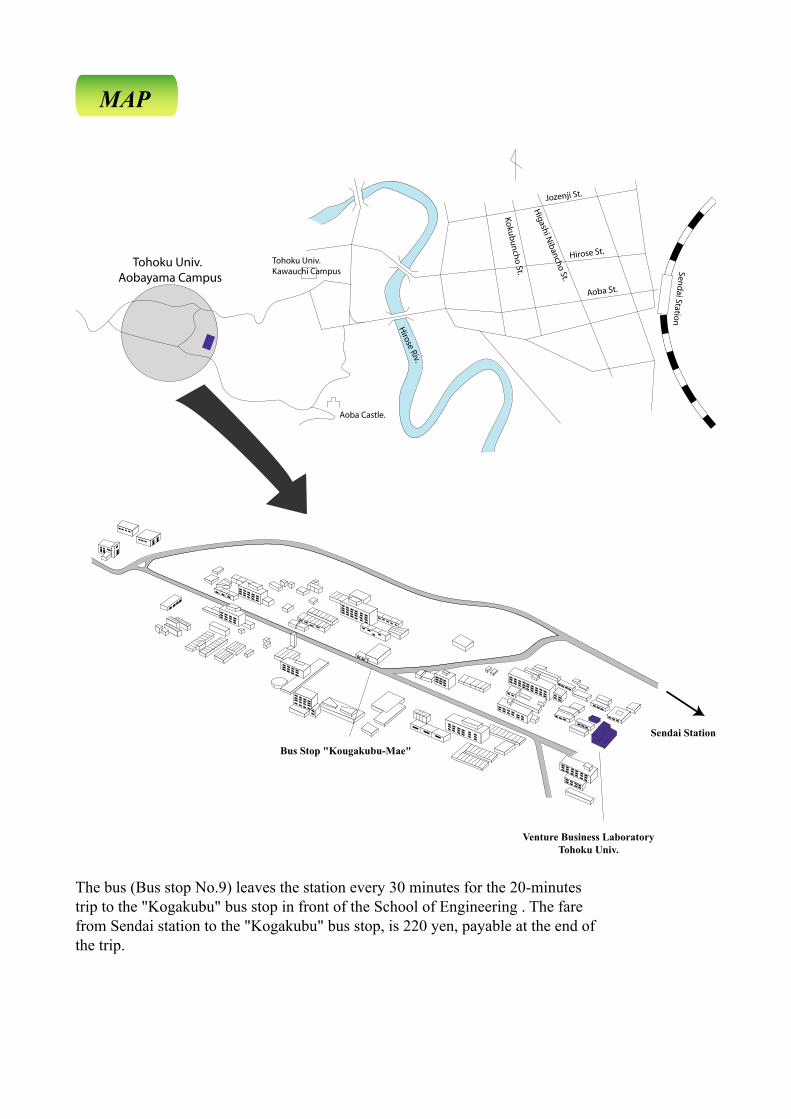
MAP
The bus (Bus stop No.9) leaves the station every 30 minutes for the 20-minutes trip to the "Kogakubu" bus stop in front of the School of Engineering . The fare from Sendai station to the "Kogakubu" bus stop, is 220 yen, payable at the end of the trip.
Tohoku Univ.Aobayama Campus
Tohoku Univ.Kawauchi Campus
Aoba Castle.
Hirose Riv.
Kokubuncho St.
Higashi N
ibancho St.
Jozenji St.
Hirose St.
Aoba St.
Send
ai Station
Bus Stop "Kougakubu-Mae"
Venture Business LaboratoryTohoku Univ.
Sendai Station