Embed Size (px)
Citation preview

VARISCITE LTD.
VAR-SOM-AM35 Datasheet Texas Instruments AM 35xx based System-On-Module

VARISCITE LTD.
VAR-SOM-AM35Data Sheet
© 2010 Variscite Ltd. All Rights Reserved. No part of this document may be photocopied, reproduced, stored in a retrieval system, or transmitted, in any form or by any means whether, electronic, Mechanical, or otherwise without the prior written permission of Variscite Ltd. No warranty of accuracy is given concerning the contents of the information contained in this publication. To the extent permitted by law no liability (including liability to any person by reason of negligence) will be accepted by Variscite Ltd., its subsidiaries or employees for any direct or indirect loss or damage caused by omissions from or inaccuracies in this document. Variscite Ltd. reserves the right to change details in this publication without notice. Product and company names herein may be the trademarks of their respective owners. Variscite Ltd. 60 Medinat Hayudim st. Hertzelia Pituach P.O.B 12598 46722, Israel Phone +972 (9) 9562910 • Fax +972 (9) 9589477

Revision History
Revision Date Notes
1.0 01/07/2010 Initial
1.1 01/11/2010 Revised block diagram
1.11 01/2/2011 Section 4.8: Added SPI options
1.12 01/3/2011 Section 4.7: McBSP signals clarification Industrial temperature support added for VAR-SOM-AM35
1.13 05/3/2011 TV-out support added
1.14 21/3/2011 Extended SOM connector signal list
1.15 2/5/2011 Power consumption specifications MMC1_DAT6 typo fix
1.16 28/5/2011 Section 8: MTBF Clarifications Section 7: VIO digital lines output voltage clarifications
1.2 6/6/2011 Section 3: GPIO 157 (pin185), type fixed from GPIO 127
1.21 20/6/2011 Section 4.6.1: USB Host signals typo fixed. CustomBoard v2.2 schematics are correct.
1.22 2/8/2011 Section 3: I2C2 pins are as listed previously, and as shown in reference schematics. Sitara pins (W1,W2) definitions were in-correct.
1.23 9/9/2011 Revised SOM drawing JTAG connection note.
1.24 3/3/2012 Section 4.8 Pin numbering typos revised.
1.3 16/3/2012 Section 6 VBAT power-on / power-off requirements
Table of Contents
Revision History .............................................................................. iii
1 Overview ........................................................................ 1
1.1 General Information .............................................................. 1
1.2 Feature Summary ................................................................. 2
1.3 Block Diagram ...................................................................... 3
2 HW Components ........................................................... 4
2.1 Texas Instruments AM35xx .................................................. 4
2.1.1 Overview ....................................................................................... 4
2.1.2 AM3517 block diagram ................................................................. 5
2.1.3 MPU Subsystem ........................................................................... 6
2.1.4 On-Chip Memory........................................................................... 6
2.1.5 External Memory Interfaces .......................................................... 6
2.1.6 DMA Controllers............................................................................ 7
2.1.7 Multimedia ..................................................................................... 7
2.1.8 Peripherals .................................................................................... 8
2.2 TPS65023 PMIC ................................................................ 10
2.3 Memory .............................................................................. 11
2.3.1 DDR2 SDRAM ............................................................................ 11
2.3.2 Non-volatile storage memory ...................................................... 11

2.4 Micrel™ KSZ8041RNL Ethernet phy .................................. 11
3 SOM Connectors ......................................................... 13
4 Interfaces ..................................................................... 27
4.1 Display interface ................................................................. 27
4.2 Analog Audio ...................................................................... 28
4.3 Camera Interface ................................................................ 28
4.4 Ethernet .............................................................................. 30
4.5 UARTs ................................................................................ 31
4.6 USB 2.0 .............................................................................. 32
4.6.1 USB 2.0 Host .............................................................................. 32
4.6.2 USB 2.0 On-The-Go ................................................................... 32
4.7 McBSP ............................................................................... 34
4.8 SPI ..................................................................................... 35
4.9 I2C ...................................................................................... 36
4.10 HDQ/1-Wire ........................................................................ 36
4.11 SD / MMC ........................................................................... 37
4.12 PWM .................................................................................. 38
4.13 Local Bus ........................................................................... 39
4.14 Touch Screen ..................................................................... 41
4.15 JTAG .................................................................................. 42
4.16 Can Bus cotroller ................................................................ 43
4.17 Boot Option ........................................................................ 44
4.18 General Purpose IOs .......................................................... 45

4.19 General System signals ..................................................... 45
4.20 RTC .................................................................................... 45
4.21 TV-OUT .............................................................................. 46
4.22 Power supply pins .............................................................. 46
5 Absolute maximum Characteristics........................... 47
6 Operational Characteristics ....................................... 47
6.1 Supply voltages .................................................................. 47
6.2 VBAT power-on / power-off sequence ................................ 47
6.3 Typical power consumption ................................................ 47
7 DC electrical characteristics ...................................... 48
8 Environmental specifications..................................... 48
9 Mechanical drawings .................................................. 49
10 Legal notice ................................................................. 50
11 Warranty terms ............................................................ 51
12 Contact information .................................................... 52

V A R - S O M - A M 3 5 S Y S T E M O N M O D U L E
1
1 Overview This chapter gives a short overview of the VAR-SOM-AM35
1.1 General Information
The VAR-SOM-AM35 is a low-power; high performance System-on-module which serves as a building block and easily integrates into any embedded solution. It includes all vital peripherals / interfaces and is ready to run any embedded operating system such as Linux and WinCE.
Supporting products:
Windows Embedded CE 6.0 R3 BSP
Linux BSP based on kernel 2.6.32
VAR-3xxCustomBoard – evaluation board
Base-Board, compatible with VAR-SOM-AM35
Windows CE 6.0 run-time image
Linux Kernel 2.6.32 sources files
Schematics
Contact support for further information: mailto:[email protected].

V A R - S O M - A M 3 5 S Y S T E M O N M O D U L E
2
1.2 Feature Summary
Texas Instruments AM3517/05 CPU
Up to 600-MHz ARM Cortex™-A8 Core
NEON™ SIMD Coprocessor
128-512MB 400MHz DDR2 SDRAM.
256-512Mbytes Flash Disk
LCD interface. Up to 2048x2048 maximum Resolution
NTSC / PAL TV-OUT
2 SD card/SDIO/MMC card interface
Power
Single 3.3-6V DC-IN power supply.(One lithium-ion cell battery)
Typical power consumption: 1W
RAW image-sensor module interface
4 UART ports
100Mbit Ethernet controller
Audio
16-bit linear audio stereo DAC (96, 48, 44.1, and 32 kHz and derivatives)
16-bit linear audio stereo ADC (48, 44.1, and 32 kHz and derivatives)
Microphone input
Line In and Out
USB
2xUSB 2.0 Host interface.
USB 2.0 OTG interface.
Touch Screen interface
Can Bus controller
Serial controllers
TDM interface (over McBSP1)
3 x SPI interface
2 x I2C interface
1 – Wire/ HDQ
V A R - S O M - A M 3 5 S Y S T E M O N M O D U L E
3
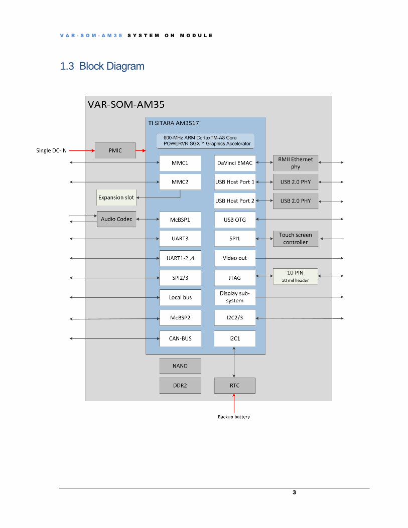
1.3 Block Diagram
V A R - S O M - A M 3 5 S Y S T E M O N M O D U L E
4
2 HW Components This chapter shortly describes the VAR-SOM-AM35 HW components.
2.1 Texas Instruments AM35xx
2.1.1 Overview
AM3517/05 high-performance, industrial applications processors with video, image, and graphics processors.
The device supports high-level operating systems (OSs), such as:
Linux
Windows CE
The following subsystems are part of the device:
Microprocessor unit (MPU) subsystem based on the ARM Cortex-A8 microprocessor
POWERVR SGX™ Graphics Accelerator (AM3517 Device only) Subsystem for 3D graphics acceleration to support display and gaming effects (3517 only)
Display subsystem with several features for multiple concurrent image manipulation, and a programmable interface supporting a wide variety of displays.
High performance interconnects provide high-bandwidth data transfers for multiple initiators to the internal and external memory controllers and to on-chip peripherals. The device also offers a
Comprehensive clock-management scheme.

V A R - S O M - A M 3 5 S Y S T E M O N M O D U L E
5
2.1.2 AM3517 block diagram

V A R - S O M - A M 3 5 S Y S T E M O N M O D U L E
6
2.1.3 MPU Subsystem
The MPU subsystem integrates the following modules
ARM subchip
– ARM® Cortex™-A8 core
– ARM Version 7™ ISA: Standard ARM instruction set + Thumb®-2, Jazelle® RCT Java accelerator, and media extensions
NEON™ SIMD coprocessor (VFP lite + media streaming instructions)
Cache memories . 16KB instruction and 16KB data—4-way set associative cache, 64 bytes/line
2.1.4 On-Chip Memory
On-chip memory configuration offers memory resources for program and data storage:
112KB ROM
64KB single-access static random access memory (SRAM)
2.1.5 External Memory Interfaces
The device includes two external memory interfaces:
General-purpose memory controller (GPMC)
– NOR flash, NAND flash (with ECC Hamming code calculation), SRAM and Pseudo-SRAM asynchronous and synchronous protocols – Flexible asynchronous protocol control for external ASIC or peripheral interfacing – 16-bit data, up to 8 chip-selects (CSs) – 128M-byte addressable per chip-select, 1G-byte total address space – Nonmultiplexed device with limited address (2K bytes)
SDRAM controller (SDRC)
– Double data rate (DDR2) SDRAM – 16-bit or 32-bit data, 2 chip-selects, configurations for a maximum of 1 G-byte address space per chip-select
V A R - S O M - A M 3 5 S Y S T E M O N M O D U L E
7
2.1.6 DMA Controllers
The device embeds one generic DMA controller, the system DMA (sDMA) controller, used for memory-to-memory, memory-to-peripheral, and peripheral-to-memory transfers:
One read port, one write port
32 prioritizable logical channels
96 hardware requests
256 x 32-bit FIFO dynamically allocable between active channels
2.1.7 Multimedia
The device uses the following multimedia accelerators for display and gaming effects as well as high-end imaging and video applications:
2D and 3D graphics accelerator (SGX) – 2D and 3D graphics and video codecs supported on common hardware – Tile-based architecture – Universal scalable shader engine (USSE™) multithreaded engine incorporating pixel and vertex shader functionality reducing die area – Advanced shader feature set in excess of Microsoft VS3.0, PS3.0, and OGL2.0 – Industry standard API support Direct3D mobile, OGL-ES 1.1 and 2.0, OpenVG 1.0, OpenMax – Fine-grained task switching, load balancing, and power management – Programmable high-quality image anti-aliasing – Advanced geometry DMA driven operation for minimum CPU interaction – Fully virtualized memory addressing for OS operation in a unified memory architecture – Advanced and standard 2D operations (that is, vector graphics, BLTs, ROPs, etc.)
Camera interface – Supports most of the raw image sensors available in the market – Includes video processing hardware – 12-bit parallel interface supported – Pixel clock up to 83 MHz
Display interface – Display controller – Color and monochrome displays up to 2048 x 2048 x 24-bpp resolution – 256 x 24-bit entries palette in red, green, blue (RGB) – 3,375 colors, 15 grayscales – Picture-in-picture (overlay), color-space conversion, rotation, color-phase rotation, and resizing support – Remote frame buffer interface – Liquid-crystal display (LCD) pixel interfaces (MIPI DPI 1.0) and LCD bus interfaces (MIPI DBI 1.0) supported
V A R - S O M - A M 3 5 S Y S T E M O N M O D U L E
8
– NTSC/PAL video encoder outputs with integrated digital-to-analog converters (DACs) output are supported on CVBS and S-video TV analog output signals – Serial display interface implements high-speed differential output buffers to support FlatLink3G™, Mobile CMADS and MIPI DSI 1.0 formats – Embedded DMA controller
2.1.8 Peripherals
The device supports a comprehensive set of peripherals to provide flexible and high-speed interfacing and on-chip programming resources. The following table provides a list and description of the peripherals available on the VAR-SOM-AM35device.
Type Name Description
Seri
al C
om
mu
nic
atio
n
Multi-channel Buffered
The McBSPs provide a full-duplex direct serial interface between Serial Ports (McBSPs) the device and other devices in a system such as audio and voice codecs and other application chips. McBSP1, McBSP2, and McBSP3 serve as general purpose serial ports while McBSP2 and McBSP3 include additional audio-loopback capability.
Multi-channel Serial Port
The McSPIs provide a master/slave interface to SPI devices. Interface (McSPI)
High-speed USB OTG
High-speed USB2.0 OTG controller that offers high-speed data Controller
HDQ/1-Wire The HDQ/1-Wire interface supports the Benchmark HDQ protocol and the Dallas Semiconductor 1-Wire protocol.
Universal Asynchronous
Serial communication interfaces compatible to the industry Receiver/Transmitter standard TL16C550 asynchronous communications element. (UART) UART1 and UART 2 are general serial communication interfaces. UART3 provides additional support for infrared data association (IrDA) and consumer infrared (CIR) communications
High-speed (HS) I2C Master/slave I2C high-speed standard interfaces with support for Inter-integrated Circuit standard mode (up to 100K bits/s), fast mode (up to 400K (I2C) Controllers bits/s), and high-speed mode (up to 3.4M bits/s).
Rem
ovab
l
e M
ed
ia
Multimedia Card/Secure Digital/Secure Digital IO (MMC/SDIO) Card Interface
MMC memory card, SD memory card, or SDIO cards interface.
Mis
cellan
eo
us
GP timers Twelve general-purpose timers
Watchdog timers Three watchdog timers (WDTs)
32-kHz synchronization timer
32-kHz clock timer
General-purpose input/output (GPIO)
General-purpose input/output pins controlled by six GPIO controllers.
Control module I/O multiplexing and chip-configuration control.

V A R - S O M - A M 3 5 S Y S T E M O N M O D U L E
9
Se
cu
rity
Mo
du
les RNG, Fast PKA, 2xDES/3DES, SHA1/MD5, SHA2/MD5, 2xAES,
Secure Watchdog Timer, and universal subscriber identity module (USIM).

V A R - S O M - A M 3 5 S Y S T E M O N M O D U L E
10
2.2 TPS65023 PMIC
The VAR-SOM-AM35 uses the TI TPS65023 companion chip.
The TPS65023 is a power-management IC dedicated for the DaVinci / AM Platforms and provides all required power sources to power the VAR-SOM-AM35.

V A R - S O M - A M 3 5 S Y S T E M O N M O D U L E
11
2.3 Memory
2.3.1 DDR2 SDRAM
The VAR-SOM-AM35 is assembled with up to 512MB of DDR2 SDRAM. 32-bit bus.
2.3.2 Non-volatile storage memory
The VAR-SOM-AM35 supports up to 512MB of SLC NAND flash.
The NAND flash is used for Flash Disk purposes, O.S. run-time-image and the Bootloader (Boot from NAND).
2.4 Micrel™ KSZ8041RNL Ethernet phy
Operating at 1.8 volts to meet low voltage and low -power requirements, the KSZ8041NL is a 10BASET/100BASE-TX Physical Layer Transceiver with MII / RMII interfaces to transmit and receive data. A unique mixed signal design extends signaling distance while reducing power consumption.
HP Auto MDI/MDI-X provides the most robust solution for eliminating the need to differentiate between crossover and straight-through cables.
The KSZ8041NL represents a new level of features and performance and is an ideal choice of physical layer transactions.
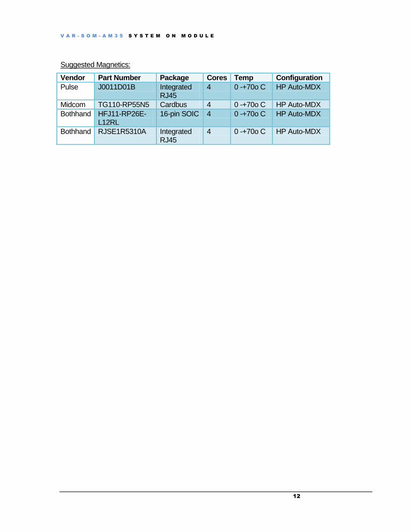
Qualified and Suggested Magnetics:
Magnetics listed under “Qualified” title have been tested in order to verify the proper operation with the KSZ8041RNL device. Magnetics in “Suggested” category was evaluated on the vendor-supplied datasheet level, but have not been tested.
Qualified Magnetics:
Vendor Part Number Package Cores Temp Configuration
Pulse H1102 16-pin SOIC 4 0 -+70o C HP Auto-MDX
Halo TG110-RP55N5 16-pin SOIC 4 0 -+70o C HP Auto-MDX
Halo HFJ11-RP26E-L12RL
Integrated RJ45
4 0 -+70o C HP Auto-MDX POE
Delta RJSE1R5310A Integrated RJ45
4 0 -+70o C HP Auto-MDX
V A R - S O M - A M 3 5 S Y S T E M O N M O D U L E
12
Suggested Magnetics:
Vendor Part Number Package Cores Temp Configuration
Pulse J0011D01B Integrated RJ45
4 0 -+70o C HP Auto-MDX
Midcom TG110-RP55N5 Cardbus 4 0 -+70o C HP Auto-MDX
Bothhand HFJ11-RP26E-L12RL
16-pin SOIC 4 0 -+70o C HP Auto-MDX
Bothhand RJSE1R5310A Integrated RJ45
4 0 -+70o C HP Auto-MDX
V A R - S O M - A M 3 5 S Y S T E M O N M O D U L E
13
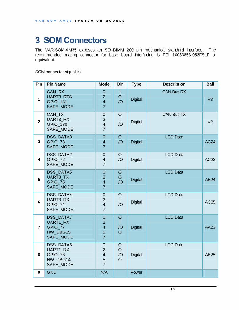
3 SOM Connectors The VAR-SOM-AM35 exposes an SO–DIMM 200 pin mechanical standard interface. The recommended mating connector for base board interfacing is FCI 10033853-052FSLF or equivalent.
SOM connector signal list:
Pin Pin Name Mode Dir Type Description Ball
1
CAN_RX UART3_RTS GPIO_131 SAFE_MODE
0 2 4 7
I O I/O
Digital
CAN Bus RX
V3
2
CAN_TX UART3_RX GPIO_130 SAFE_MODE
0 2 4 7
O I
I/O
Digital
CAN Bus TX
V2
3 DSS_DATA3 GPIO_73 SAFE_MODE
0 4 7
O I/O
Digital
LCD Data AC24
4 DSS_DATA2 GPIO_72 SAFE_MODE
0 4 7
O I/O
Digital
LCD Data AC23
5
DSS_DATA5 UART3_TX GPIO_75 SAFE_MODE
0 2 4 7
O O I/O
Digital
LCD Data
AB24
6
DSS_DATA4 UART3_RX GPIO_74 SAFE_MODE
0 2 4 7
O I
I/O
Digital
LCD Data
AC25
7
DSS_DATA7 UART1_RX GPIO_77 HW_DBG15 SAFE_MODE
0 2 4 5 7
O I
I/O O
Digital
LCD Data
AA23
8
DSS_DATA6 UART1_RX GPIO_76 HW_DBG14 SAFE_MODE
0 2 4 5 7
O O I/O O
Digital
LCD Data
AB25
9 GND N/A Power

V A R - S O M - A M 3 5 S Y S T E M O N M O D U L E
14
10 GND N/A Power
11 DSS_DATA11 GPIO_81 SAFE_MODE
0 4 7
O I/O
Digital
LCD Data Y23
12 DSS_DATA10 GPIO_80 SAFE_MODE
0 4 7
O I/O
Digital
LCD Data Y22
13 DSS_DATA13 GPIO_83 SAFE_MODE
0 4 7
O I/O
Digital
LCD Data Y25
14 DSS_DATA12 GPIO_82 SAFE_MODE
0 4 7
O I/O
Digital
LCD Data Y24
15 DSS_DATA15 GPIO_85 SAFE_MODE
0 4 7
O I/O
Digital
LCD Data W22
16 DSS_DATA14 GPIO_84 SAFE_MODE
0 4 7
O I/O
Digital
LCD Data W21
17 DSS_DATA17 GPIO_87 SAFE_MODE
0 4 7
O I/O
Digital
LCD Data W24
18
CAM_D5 GPIO_104 HW_DBG7 SAFE_MODE
0 4 5 7
I I/O O
Digital
ISP Data
Y6
19
DSS_DATA19 McSPI3_SIMO DSS_DATA3 GPIO_89 SAFE_MODE
0 2 3 4 7
O I/O O I/O
Digital
LCD Data
V24
20
DSS_DATA18 McSPI3_CLK DSS_DATA4 GPIO_88 SAFE_MODE
0 2 3 4 7
O I/O O I/O
Digital
LCD Data
W25
21
DSS_DATA21 McSPI3_CS0 DSS_DATA1 GPIO_91 SAFE_MODE
0 2 3 4 7
O I/O O I/O
Digital
LCD Data
U21
V A R - S O M - A M 3 5 S Y S T E M O N M O D U L E
15
22
DSS_DATA20 McSPI3_SOMI DSS_DATA2 GPIO_90 SAFE_MODE
0 2 3 4 7
O I/O O I/O
Digital
LCD Data
V25
23
DSS_DATA23 DSS_DATA5 GPIO_93 SAFE_MODE
0 3 4 7
O O I/O
Digital
LCD Data
U23
24
DSS_DATA22 McSPI3_CS1 DSS_DATA0 GPIO_92 SAFE_MODE
0 2 3 4 7
O O O I/O
Digital
LCD Data
U22
25 GND N/A Power
26
DSS_HSYNC GPIO_67 HW_DBG13 SAFE_MODE
0 4 5 7
O I/O O
Digital
LCD Horizontal Sync
AD22
27 MMC1_DAT4 GPIO_126 SAFE_MODE
0 4 7
I/O I/O
Digital
AB10
28
DSS_PCLK GPIO_66 HW_DBG12 SAFE_MODE
0 4 5 7
O I/O O
Digital
LCD Pixel Clock
AE23
29 UART3_CTS GPIO_163 SAFE_MODE
0 4 7
I/O I/O
Digital
UART3 CTS N2
30 MMC1_DAT7 GPIO129 SAFE_MODE
0 4 7
I/O I/O
Digital
AE10
31 UART3_RTS GPIO_164 SAFE_MODE
0 4 7
O I/O
Digital
UART3 RTS N3
32 MMC1_CLK GPIO_120 SAFE_MODE
0 4 7
O I
Digital MMC1 Clock
AA9
33 UART3_RX GPIO_165 SAFE_MODE
0 4 7
I I/O
Digital
UART3 RX P1

V A R - S O M - A M 3 5 S Y S T E M O N M O D U L E
16
34 MMC1_DAT6 GPIO_128 SAFE_MODE
0 4 7
I/O I/O
Digital
AD10
35 UART3_TX GPIO_166 SAFE_MODE
0 4 7
O I/O
Digital
UART3 TX P2
36
MMC1_DAT0 McSPI2_CLK GPIO_122 SAFE_MODE
0 1 4 7
I/O I/O I/O
Digital
MMC1 Data 0
AC9
37 GND N/A Power
38
MMC1_DAT1 McSPI2_SIMO GPIO_123 SAFE_MODE
0 1 4 7
I/O I/O I/O
Digital
MMC1 Data 1
AD9
39 GND N/A
40
MMC1_DAT2 McSPI2_SOMI GPIO_124 SAFE_MODE
0 1 4 7
I/O I/O I/O
Digital
MMC1 Data 2
AE9
41 GND N/A Power
42
MMC1_DAT3 McSPI2_CS0 GPIO_125 SAFE_MODE
0 1 4 7
I/O O I/O
Digital
MMC#1 Data 3
AA10
43 MMC1_CMD GPIO_121 SAFE_MODE
0 4 7
I/O I/O
Digital
MMC#1 Command AB9
44 CAM_D6 GPIO_105 SAFE_MODE
0 4 7
I I/O
Digital
ISP Data AB6
45 DSS_DATA16 GPIO_86 SAFE_MODE
0 4 7
O I/O
Digital
LCD Data W23
46 DSS_VSYNC GPIO_68 SAFE_MODE
0 4 7
O I/O
Digital
LCD Vertical Sync AD23
47 GND N/A Power
48 GND N/A Power
V A R - S O M - A M 3 5 S Y S T E M O N M O D U L E
17
49 SYS_CLKOUT1 GPIO_10 SAFE_MODE
0 4 7
O I/O
Digital
General Purpose Clock-out 1 N25
50
CAM_D4 GPIO_103 HW_DBG6 SAFE_MODE
0 4 5 7
I I/O O
Digital
ISP Data
AE5
51 GND N/A Power
52 LB_nCS1 GPIO_52
0 4
O I/O
Digital Local bus Chip Select 1
L1
53 CAM_D7 GPIO_106 SAFE_MODE
0 4 7
I I/O
Digital
ISP Data AC6
54 TV-OUT O Analog
55
CAM_D3 GPIO_102 HW_DBG5 SAFE_MODE
0 4 5 7
I I/O O
Digital
ISP Data
AD5
56
CAM_D2 GPIO_101 HW_DBG4 SAFE_MODE
0 4 5 7
I I/O O
Digital
ISP Data
AC5
57
CAM_WEN CAMD9 UART4_RX GPIO_98 HW_DBG3 SAFE_MODE
0 1 2 4 5 7
I/O I I
I/O O
Digital
ISP write-enable signal ISP Data
AE3
58 GND N/A Power
59
CAM_PCLK GPIO_94 HW_DBG0 SAFE_MODE
0 4 5 7
I/O I/O O
Digital
ISP Parallel interface pixel clock
AD2
60 GND N/A Power
61 I2C3_SDA GPIO_185 SAFE_MODE
0 4 7
I/OD I/O
Digital
I2C#3 SDA (data) W5
62
DSS_D9 GPIO_79 HW_DBG17 SAFE_MODE
0 4 5 7
O I/O O
Digital
LCD data
AA25

V A R - S O M - A M 3 5 S Y S T E M O N M O D U L E
18
63 I2C3_SCL GPIO_184 SAFE_MODE
0 4 7
I/OD I/O
Digital
I2C#3 SCL (clock) W4
64 DSS_ACBIAS GPIO_69 SAFE_MODE
0 4 7
O I/O
Digital
LCD AC bias/Data enable AE24
65
UART2_CTS McBSP3_DX GPT9_PWM_EVT GPIO_144 SAFE_MODE
0 1 2 4 7
I I/O I/O I/O
Digital
UART#2 CTS McBSP3 data out
F20
66
DSS_D0 UART1_CTS GPIO_70 SAFE_MODE
0 2 4 7
O I
I/O
Digital
LCD data
AD24
67
UART2_RTS McBSP3_DR GPT10_PWM_EVT GPIO_145 SAFE_MODE
0 1 2 4 7
O I
I/O I/O
Digital
UART#2 RTS McBSP3 data in
F19
68
DSS_D1 UART1_RTS GPIO_71 SAFE_MODE
0 2 4 7
O O I/O
Digital
LCD Data
AD25
69
UART2_TX McBSP3_CLKX GPT11_PWM_EVT GPIO_146 SAFE_MODE
0 1 2 4 7
O I/O I/O I/O
Digital
UART#2 TX McBSP3 clock
E24
70
DSS_DATA8 GPIO_78 HW_DBG16 SAFE_MODE
0 4 5 7
O I/O O
Digital
LCD Data
AA24
71
UART2_RX McBSP3_FSX GPT8_PWM_EVT GPIO_147 SAFE_MODE
0 1 2 4 7
I I/O I/O I/O
Digital
UART#2 RX McBSP3 frame sync
E23
72 NC N/A
73 TSPX N/A I Analog Touch Screen X Plus N/A
74 GND N/A Power
75 TSPY N/A I Analog Touch Screen Y Plus N/A

V A R - S O M - A M 3 5 S Y S T E M O N M O D U L E
19
76
CAM_VS UART4_CTS GPIO_97 HW_DBG2 SAFE_MODE
0 2 4 5 7
IO I
I/O O
Digital
ISP Frame trigger signal
AD3
77 TSMX N/A I Analog Touch Screen X Minus N/A
78
CAM_HS UART4_RTS GPIO_96 SAFE_MODE
0 2 4 7
IO O I/O
Digital
ISP Line trigger signal
AE2
79 TSMY N/A I Analog Touch Screen Y Minus N/A
80
CAM_FLD CAM_D8 UART4_TX I2C3_SCL GPIO_95 HW_DBG1 SAFE_MODE
0 1 2 3 4 5 7
I/O I O
I/OD IO O
Digital
ISP Field ID signal
AD1
81 GND N/A Power
82
HDQ SYS_ALTCLK I2C2_SCCBE I2C3_SCCBE GPIO_170 SAFE_MODE
0 1 2 3 4 7
I/O I O O I/O
Digital
HDQ / 1-Wire Line
L25
83 GND N/A Power
84 UART1_TX GPIO_148 SAFE_MODE
0 4 7
O I/O
Digital
UART#1 TX AA19
85
LB_WAIT3 SYS_nDMAREQ1 UART3_CTS GPIO_65 SAFE_MODE
0 1 2 4 7
I I I
I/O
Digital
Local Bus Wait for CS3 Local Bus SDMA Request 1
U1
86 UART1_RTS GPIO_149 SAFE_MODE
0 4 7
O I/O
Digital
UART#1 RTS Y19
87 LB_CLK GPIO_59
0 4
O I/O
Digital Local Bus clock
N1
88 UART1_CTS GPIO_150 SAFE_MODE
0 4 7
I I/O
Digital
UART#1 CTS Y20
V A R - S O M - A M 3 5 S Y S T E M O N M O D U L E
20
89
LB_nCS3 SYS_nDMAREQ0 GPT10_PWM_EVT GPIO_54 SAFE_MODE
0 1 2 4 7
O I
I/O I/O
Digital
Local bus Chip Select 3
M3
90
UART1_RX McBSP1_CLKR GPIO_151 SAFE_MODE
0 2 4 7
I I
I/O
Digital
UART#1 RX
W20
91 LB_NBE1 GPIO_61 SAFE_MODE
0 4 7
O I/O
Digital
T1
92 SYS_BOOT5 MMC2_DIR_DAT3 GPIO_7
0 1 4
I O I/O
Digital Flash burning switch
AB2
93 CAM_D1 GPIO_100 SAFE_MODE
0 4 7
I I
Digital ISP Data
AE4
94 GND N/A Power
95
CAM_D0 I2C3_SDA GPIO_99 SAFE_MODE
0 3 4 7
I I/OD
I
Digital
ISP Data
AD4
96 GND N/A Power
97 RESET_OUT_N
O Digital Reset signal to base-board
peripherals N/A
98 McBSP2_CLKX GPIO_117 SAFE_MODE
0 4 7
I/O I/O
Digital
McBSP#2 Transmit clock C25
99 I2C2_SDA GPIO_168 SAFE_MODE
0 4 7
I/OD I/O
Digital
I2C#2 SDA (data) W2
100 GND N/A Power
101 I2C2_SCL GPIO_183 SAFE_MODE
0 4 7
I/OD I/O
Digital
I2C#2 SCL (clock) W1
102 McBSP2_DR GPIO_118 SAFE_MODE
0 4 7
I I/O
Digital
McBSP#2 Receive data B25
103 USBHOST1_DP N/A IO Diff USB Host #1 Data Positive N/A
V A R - S O M - A M 3 5 S Y S T E M O N M O D U L E
21
104 McBSP2_DX GPIO_119 SAFE_MODE
0 4 7
I/O I/O
Digital
McBSP#2 Transmit data D24
105 USBHOST1_DM N/A I/O Diff USB Host #1 Data Negative N/A
106 McBSP2_FSX GPIO_116 SAFE_MODE
0 4 7
I/O I/O
Digital
McBSP#2 Receive Frame D25
107 USBHOST1_VBUS
N/A I Analog USB Host #1VBUS 5v
indicator N/A
108 GND N/A Power
109 SYS_CLKOU2 GPIO186 SAFE_MODE
0 4 7
O I/O
Digital
General purpose clkout 2 M25
110 VBAT
N/A I Power VAR-SOM-AM35 single DC-IN supply voltage. Voltage
range: 3.3 – 6V N/A
111 USBHOST2_VBUS
N/A I Analog USB Host #2 VBUS 5v
indicator N/A
112 VBAT
N/A I Power VAR-SOM-AM35 single DC-IN supply voltage. Voltage
range: 3.3 – 6V
113 GND N/A Power
114 VBAT
N/A I Power VAR-SOM-AM35 single DC-IN supply voltage. Voltage
range: 3.3 – 6V
115 GND N/A Power
116 VBAT
N/A I Power VAR-SOM-AM35 single DC-IN supply voltage. Voltage
range: 3.3 – 6V
117 VIO N/A O Power Digital IO Output Voltage.
Up to 200ma
118 USB_OTG_VBUS
N/A I Analog USB 2.0 OTG VBUS
indicator
119
LB_IO_A10 SYS_nDMAREQ3 GPIO_43 SAFE_MODE
0 1 4 7
O I
I/O
Digital
Local bus address 10
G6
120 USB_OTG_DP N/A IO Diff USB 2.0 OTG Data Positive
121 USBHOST2_DM N/A IO Diff USB Host #2 Data Negative
122 USB_OTG_DN
N/A IO Diff USB 2.0 OTG Data
Negative
V A R - S O M - A M 3 5 S Y S T E M O N M O D U L E
22
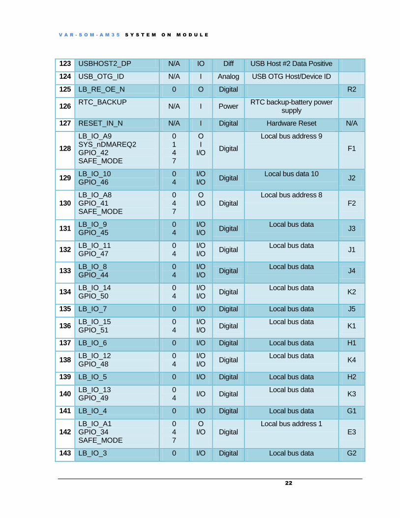
123 USBHOST2_DP N/A IO Diff USB Host #2 Data Positive
124 USB_OTG_ID N/A I Analog USB OTG Host/Device ID
125 LB_RE_OE_N 0 O Digital R2
126 RTC_BACKUP
N/A I Power RTC backup-battery power
supply
127 RESET_IN_N N/A I Digital Hardware Reset N/A
128
LB_IO_A9 SYS_nDMAREQ2 GPIO_42 SAFE_MODE
0 1 4 7
O I
I/O
Digital
Local bus address 9
F1
129 LB_IO_10 GPIO_46
0 4
I/O I/O
Digital Local bus data 10
J2
130 LB_IO_A8 GPIO_41 SAFE_MODE
0 4 7
O I/O
Digital
Local bus address 8 F2
131 LB_IO_9 GPIO_45
0 4
I/O I/O
Digital Local bus data
J3
132 LB_IO_11 GPIO_47
0 4
I/O I/O
Digital Local bus data
J1
133 LB_IO_8 GPIO_44
0 4
I/O I/O
Digital Local bus data
J4
134 LB_IO_14 GPIO_50
0 4
I/O I/O
Digital Local bus data
K2
135 LB_IO_7 0 I/O Digital Local bus data J5
136 LB_IO_15 GPIO_51
0 4
I/O I/O
Digital Local bus data
K1
137 LB_IO_6 0 I/O Digital Local bus data H1
138 LB_IO_12 GPIO_48
0 4
I/O I/O
Digital Local bus data
K4
139 LB_IO_5 0 I/O Digital Local bus data H2
140 LB_IO_13 GPIO_49
0 4
I/O Digital Local bus data
K3
141 LB_IO_4 0 I/O Digital Local bus data G1
142 LB_IO_A1 GPIO_34 SAFE_MODE
0 4 7
O I/O
Digital
Local bus address 1 E3
143 LB_IO_3 0 I/O Digital Local bus data G2

V A R - S O M - A M 3 5 S Y S T E M O N M O D U L E
23
144 LB_IO_A2 GPIO_35 SAFE_MODE
0 4 7
O I/O
Digital
Local bus address 2 E2
145 LB_IO_2 0 I/O Digital Local bus data G3
146 LB_IO_A3 GPIO_36 SAFE_MODE
0 4 7
O I/O
Digital
Local bus address 3 E1
147 LB_IO_1 0 I/O Digital Local bus data G4
148
LB_WAIT1 UART4_TX GPIO_63 SAFE_MODE
0 1 4 7
I O I/O
Digital
Local bus wait signal
T4
149 LB_IO_0 0 I/O Digital Local bus data G5
150 LB_IO_A4 GPIO_37 SAFE_MODE
0 4 7
O I/O
Digital
Local bus address 4 F7
151 GND N/A Power
152 LB_nBE0_CLE GPIO_60
0 4
O I/O
Digital
Local bus Output enable for static memory, muxed with
CLE R4
153 LB_IO_A5 GPIO_38 SAFE_MODE
0 4 7
O I/O
Digital
Local bus address 5 F6
154 LB_nADV_ALE
0 O Digital Local bus Address Latch
Enable, muxed with Address Valid
R1
155 LB_IO_A6 GPIO_39 SAFE_MODE
0 4 7
O I/O
Digital
Local bus address 6 F4
156 GND N/A Power
157 LB_IO_A7 GPIO_40 SAFE_MODE
0 4 7
O I/O
Digital
Local bus address 7 F3
158 GPMC_WAIT2 GPIO_64 SAFE_MODE
0 4 7
I/O Digital Local bus Wait 2
159 GND N/A Power
160 LB_WE_N
0 O Digital Local bus Write enable
(active low) R3

V A R - S O M - A M 3 5 S Y S T E M O N M O D U L E
24
161 LINK_LED N/A O Analog Ethernet Link LED
162 GND N/A Power
163 SPEED_LED N/A O Analog Ethernet Speed LED
164
MMC2_CLK McSPI3_CLK UART4_CTS GPIO_130 SAFE_MODE
0 1 2 4 7
O I/O I
I/O
Digital
MMC2 Clock
AD11
165 ETH_TXN N/A O Diff Ethernet TX Negative
166
MMC2_CMD McSPI3_SIMO UART4_RTS GPIO_131 SAFE_MODE
0 1 2 4 7
I/O I/O O I/O
Digital
MMC2 CMD
AE11
167 ETH_TXP N/A O Diff Ethernet TX Positive
168
MMC2_DAT0 McSPI3_SOMI UART4_TX GPIO_132 SAFE_MODE
0 1 2 4 7
I/O I/O O I/O
Digital
MMC2 Data 0
AB12
169 VCC33A
O Power 3.3V Output to Ethernet
Magnetics
170
MMC2_DAT1 UART4_RX GPIO_133 SAFE_MODE
0 2 4 7
I/O I
I/O
Digital
MMC2 Data 1
AC12
171 ETH_RXN I Diff Ethernet RX Negative
172
MMC2_DAT2 McSPI3_CS1 GPIO_134 SAFE_MODE
0 1 4 7
I/O O I/O
Digital
MMC2 Data 2
AD12
173 ETH_RXP I Diff Ethernet RX Positive
174
MMC2_DAT3 McSPI3_CS0 GPIO_135 SAFE_MODE
0 1 4 7
I/O I/O I/O
Digital
MMC2 Data 3
AE12
175
McBSP3_FSX UART2_RX GPIO_143 SAFE_MODE
0 1 4 7
I/O I
I/O
Digital
C23

V A R - S O M - A M 3 5 S Y S T E M O N M O D U L E
25
176
McBSP4_DR GPIO_153 MM_FS_USB3_RXRCV SAFE_MODE
0 4 6 7
I I/O I/O
Digital
A23
177
McBSP3_CLKX UART2_TX GPIO_142 SAFE_MODE
0 1 4 7
I/O O I/O
Digital
A24
178 GND N/A Power
179 GND N/A Power
180 GND N/A Power
181 GND N/A Power
182 GND N/A Power
183
McBSP1_CLKR GPIO_156 SAFE_MODE
0 4 7
I/O I/O
Digital
R25
184 GND N/A Power
185 McBSP1_FSR GPIO157 SAFE_MODE
0 4 7
I/O I/O
Digital
P21
186 AUDIO_IN_L N/A I Analog Audio Line in left
187
McBSP1_CLKS GPIO160 UART1_CTS SAFE_MODE
0 4 5 7
I I/O I
Digital
P25
188 AUDIO_IN_R N/A I Analog Audio line in Right
189
LB_nCS4 SYS_nDMAREQ1 GPT9_PWM_EVT GPIO_55 SAFE_MODE
0 1 3 4 7
O I
I/O I/O
Digital
PWM signal
M2
190 HP_LOUT N/A O Analog Headphones Left
191
MMC2_DAT4 MMC2_DIR_DAT0 MMC3_DAT0 GPIO_136 SAFE_MODE
0 1 3 4 7
I/O O I/O I/O
Digital
MMC2 Data 4
AB13
192 HP_ROUT N/A O Analog Headphones right

V A R - S O M - A M 3 5 S Y S T E M O N M O D U L E
26
193
MMC2_DAT5 MMC2_DIR_DAT1 MMC3_DAT1 GPIO_137 MM_FSUSB3_RXDP SAFE_MODE
0 1 3 4 6 7
I/O O I/O I/O I/O
Digital
MMC2 Data 5
AC13
194 GND N/A Power
195
MMC2_DAT6 MMC2_DIR_CMD MMC3_DAT2 GPIO_138 SAFE_MODE
0 1 3 4 7
I/O O I/O I/O
Digital
MMC2 Data 6
AD13
196 MIC_BIAS N/A O Analog Microphone Bias voltage
197 MIC_IN N/A I Analog Microphone in
198 GND N/A Power
199
MMC2_DAT7 MMC2_CLKIN MMC3_DAT3 GPIO_139 MM_FSUSB_RXDM SAFE_MODE
0 1 3 4 6 7
I/O I
I/O I/O I/O
Digital
MMC2 Data 7
AE13
200 GND N/A Power
V A R - S O M - A M 3 5 S Y S T E M O N M O D U L E
27
4 Interfaces
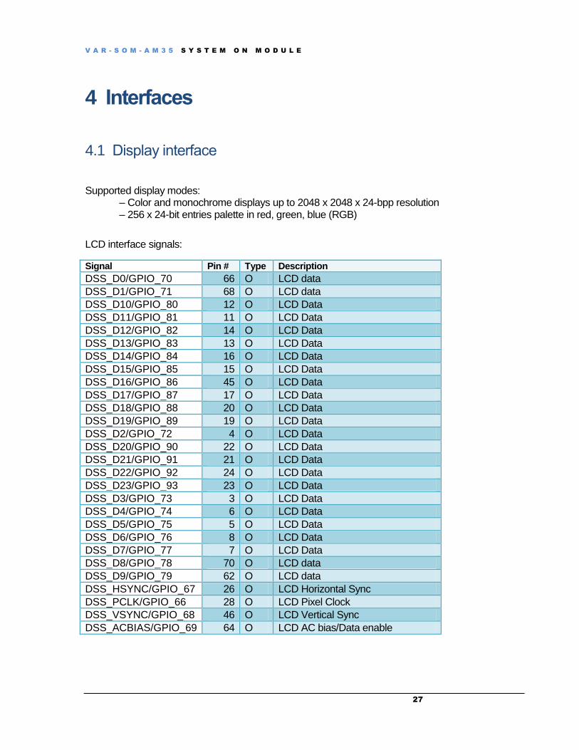
4.1 Display interface
Supported display modes: – Color and monochrome displays up to 2048 x 2048 x 24-bpp resolution – 256 x 24-bit entries palette in red, green, blue (RGB)
LCD interface signals:
Signal Pin # Type Description
DSS_D0/GPIO_70 66 O LCD data
DSS_D1/GPIO_71 68 O LCD data
DSS_D10/GPIO_80 12 O LCD Data
DSS_D11/GPIO_81 11 O LCD Data
DSS_D12/GPIO_82 14 O LCD Data
DSS_D13/GPIO_83 13 O LCD Data
DSS_D14/GPIO_84 16 O LCD Data
DSS_D15/GPIO_85 15 O LCD Data
DSS_D16/GPIO_86 45 O LCD Data
DSS_D17/GPIO_87 17 O LCD Data
DSS_D18/GPIO_88 20 O LCD Data
DSS_D19/GPIO_89 19 O LCD Data
DSS_D2/GPIO_72 4 O LCD Data
DSS_D20/GPIO_90 22 O LCD Data
DSS_D21/GPIO_91 21 O LCD Data
DSS_D22/GPIO_92 24 O LCD Data
DSS_D23/GPIO_93 23 O LCD Data
DSS_D3/GPIO_73 3 O LCD Data
DSS_D4/GPIO_74 6 O LCD Data
DSS_D5/GPIO_75 5 O LCD Data
DSS_D6/GPIO_76 8 O LCD Data
DSS_D7/GPIO_77 7 O LCD Data
DSS_D8/GPIO_78 70 O LCD data
DSS_D9/GPIO_79 62 O LCD data
DSS_HSYNC/GPIO_67 26 O LCD Horizontal Sync
DSS_PCLK/GPIO_66 28 O LCD Pixel Clock
DSS_VSYNC/GPIO_68 46 O LCD Vertical Sync
DSS_ACBIAS/GPIO_69 64 O LCD AC bias/Data enable
V A R - S O M - A M 3 5 S Y S T E M O N M O D U L E
28
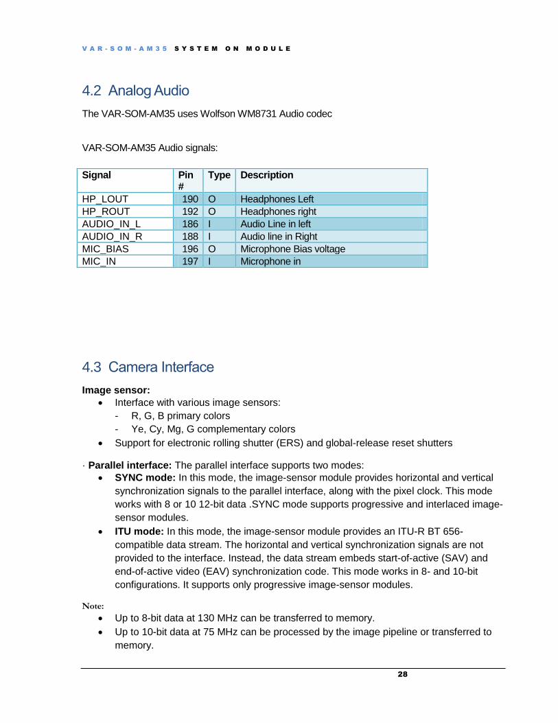
4.2 Analog Audio
The VAR-SOM-AM35 uses Wolfson WM8731 Audio codec
VAR-SOM-AM35 Audio signals:
4.3 Camera Interface
Image sensor:
Interface with various image sensors:
- R, G, B primary colors
- Ye, Cy, Mg, G complementary colors
Support for electronic rolling shutter (ERS) and global-release reset shutters
· Parallel interface: The parallel interface supports two modes:
SYNC mode: In this mode, the image-sensor module provides horizontal and vertical
synchronization signals to the parallel interface, along with the pixel clock. This mode
works with 8 or 10 12-bit data .SYNC mode supports progressive and interlaced image-
sensor modules.
ITU mode: In this mode, the image-sensor module provides an ITU-R BT 656-
compatible data stream. The horizontal and vertical synchronization signals are not
provided to the interface. Instead, the data stream embeds start-of-active (SAV) and
end-of-active video (EAV) synchronization code. This mode works in 8- and 10-bit
configurations. It supports only progressive image-sensor modules.
Note:
Up to 8-bit data at 130 MHz can be transferred to memory.
Up to 10-bit data at 75 MHz can be processed by the image pipeline or transferred to
memory.
Signal Pin #
Type Description
HP_LOUT 190 O Headphones Left
HP_ROUT 192 O Headphones right
AUDIO_IN_L 186 I Audio Line in left
AUDIO_IN_R 188 I Audio line in Right
MIC_BIAS 196 O Microphone Bias voltage
MIC_IN 197 I Microphone in

V A R - S O M - A M 3 5 S Y S T E M O N M O D U L E
29
Up to 12-bit data at 75 MHz can be transferred to memory as is, or after processing
inside the CCDC. It can also be internally converted to 10-bit data for full processing.
VAR-SOM-AM35 ISP signals:
Note: UART4 signals are multiplexed with Camera interface
Signal Pin #
Type
Description
CAM_D0/GPIO_99 95 I ISP Data
CAM_D1/GPIO_100 93 I ISP Data
CAM_D2/GPIO_101 56 I ISP Data
CAM_D3/GPIO_102 55 I ISP Data
CAM_D4/GPIO_103 50 I ISP Data
CAM_D5/GPIO_104 18 I ISP Data
CAM_D6/GPIO_105 44 I ISP Data
CAM_D7/GPIO_106 53 I ISP Data
CAM_FLD/CAMD8/GPIO_95 80 IO ISP Field identification input/output signal
CAM_HS/GPIO_96 78 IO ISP Line trigger input/output signal
CAM_PCLK/GPIO_94 59 I ISP Parallel interface pixel clock
CAM_VS/GPIO_97 76 IO ISP Frame trigger input/output signal
CAM_WEN/CAMD9/GPIO_98 57 I ISP External write-enable signal / Data

V A R - S O M - A M 3 5 S Y S T E M O N M O D U L E
30
4.4 Ethernet
The VAR-SOM-AM35 provides one full-featured 10/100 Mbit Ethernet port using the on-chip MAC controller, and Micrel™ KSZ8041RNL Ethernet phy
Features:
Fully compliant with IEEE 802.3/802.3u standards
Integrated Ethernet MAC and PHY
10BASE-T and 100BASE-TX support
Full- and Half-duplex support
Full-duplex flow control
Backpressure for half-duplex flow control
Preamble generation and removal
Automatic 32-bit CRC generation and checking
Automatic payload padding and pad removal
Auto-negotiation
Automatic polarity detection and correction
VAR-SOM-AM35 Ethernet Controller signals:
Signal Pin # Type Description
ETH_RXN 171 I Ethernet RX Negative
ETH_RXP 173 I Ethernet RX Positive
ETH_TXN 165 O Ethernet TX Negative
ETH_TXP 167 O Ethernet TX Positive
SPEED_LED 163 O Ethernet Speed LED, active low
LINK_LED 161 O Ethernet Link LED, , active low
VCC33A 169 O 3.3V Output to Ethernet Magnetics

V A R - S O M - A M 3 5 S Y S T E M O N M O D U L E
31
4.5 UARTs
The VAR-SOM-AM35 has 4 UART ports.
Each UART includes a programmable baud-rate generator. Each port supports baud rates up to 3.6Mbits.
Receive and transmit FIFO fill and drain operations can be done using programmed IO or DMA transfers. To minimize CPU overhead for UART communications, device driver software can setup interrupts and DMA for data transfers to/from memory.
VAR-SOM-AM35 UART1 signals:
VAR-SOM-AM35 UART2 signals:
VAR-SOM-AM35 UART3 signals:
VAR-SOM-AM35 UART4 signals:
Note: UART4 signals are multiplexed with Camera interface
Signal Pin # Type Description
UART1_CTS/GPIO_150 88 I UART#1 CTS
UART1_RTS/GPIO_149 86 O UART#1 RTS
UART1_RX/GPIO_151 90 I UART#1 RX
UART1_TX/GPIO_148 84 O UART#1 TX
Signal Pin # Type Description
UART2_CTS/GPIO_144 65 I UART#2 CTS
UART2_RTS/GPIO_145 67 O UART#2 RTS
UART2_RX/GPIO_147 71 I UART#2 RX
UART2_TX/GPIO_146 69 O UART#2 TX
Signal Pin # Type Description
UART3_CTS/GPIO_163 29 I UART#3 CTS
UART3_RTS/GPIO_164 31 O UART#3 RTS
UART3_RX/GPIO_165 33 I UART#3 RX
UART3_TX/GPIO_166 35 O UART#3 TX
Signal Pin # Type Description
UART4_CTS/CAM_VS/GPIO_97 76 I UART#4 CTS
UART4_TX/CAMD8/GPIO_95 80 O UART#4 TX
UART4_RTS/CAM_HS/GPIO_96 78 O UART#4 RTS
UART4_RX/CAMD9/GPIO_98 57 I UART#4 RX
V A R - S O M - A M 3 5 S Y S T E M O N M O D U L E
32
4.6 USB 2.0
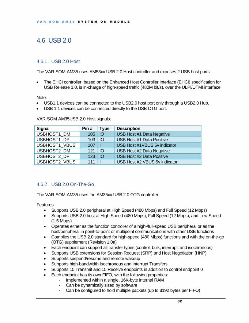
4.6.1 USB 2.0 Host
The VAR-SOM-AM35 uses AM53xx USB 2.0 Host controller and exposes 2 USB host ports.
The EHCI controller, based on the Enhanced Host Controller Interface (EHCI) specification for USB Release 1.0, is in-charge of high-speed traffic (480M bit/s), over the ULPI/UTMI interface
Note:
USB1.1 devices can be connected to the USB2.0 host port only through a USB2.0 Hub.
USB 1.1 devices can be connected directly to the USB OTG port.
VAR-SOM-AM35USB 2.0 Host signals:
4.6.2 USB 2.0 On-The-Go
The VAR-SOM-AM35 uses the AM35xx USB 2.0 OTG controller
Features:
Supports USB 2.0 peripheral at High Speed (480 Mbps) and Full Speed (12 Mbps)
Supports USB 2.0 host at High Speed (480 Mbps), Full Speed (12 Mbps), and Low Speed (1.5 Mbps)
Operates either as the function controller of a high-/full-speed USB peripheral or as the host/peripheral in point-to-point or multipoint communications with other USB functions
Complies the USB 2.0 standard for high-speed (480 Mbps) functions and with the on-the-go (OTG) supplement (Revision 1.0a)
Each endpoint can support all transfer types (control, bulk, interrupt, and isochronous)
Supports USB extensions for Session Request (SRP) and Host Negotiation (HNP)
Supports suspend/resume and remote wakeup
Supports high-bandwidth Isochronous and Interrupt Transfers
Supports 15 Transmit and 15 Receive endpoints in addition to control endpoint 0
Each endpoint has its own FIFO, with the following properties: - Implemented within a single, 16K-byte internal RAM - Can be dynamically sized by software - Can be configured to hold multiple packets (up to 8192 bytes per FIFO)
Signal Pin # Type Description
USBHOST1_DM 105 IO USB Host #1 Data Negative
USBHOST1_DP 103 IO USB Host #1 Data Positive
USBHOST1_VBUS 107 I USB Host #1VBUS 5v indicator
USBHOST2_DM 121 IO USB Host #2 Data Negative
USBHOST2_DP 123 IO USB Host #2 Data Positive
USBHOST2_VBUS 111 I USB Host #2 VBUS 5v indicator

V A R - S O M - A M 3 5 S Y S T E M O N M O D U L E
33
- can be accessed either by direct access of by DMA controller
Software connect/disconnect option for peripheral
Performs all transaction scheduling in hardware VAR-SOM-AM35 USB 2.0 OTG signals:
Note: external LDO is required in host mode, see reference schematics
USB_OTG_VBUS functionality:
Client mode: used as an indication of host presence. Host mode: not used.
Signal Pin #
Type Description
USB_OTG_DN 122 IO USB 2.0 OTG Data Negative
USB_OTG_DP 120 IO USB 2.0 OTG Data Positive
USB_OTG_ID 124 I USB OTG Host/Client ID
USB_OTG_VBUS 118 I USB 2.0 OTG VBUS indicator
V A R - S O M - A M 3 5 S Y S T E M O N M O D U L E
34
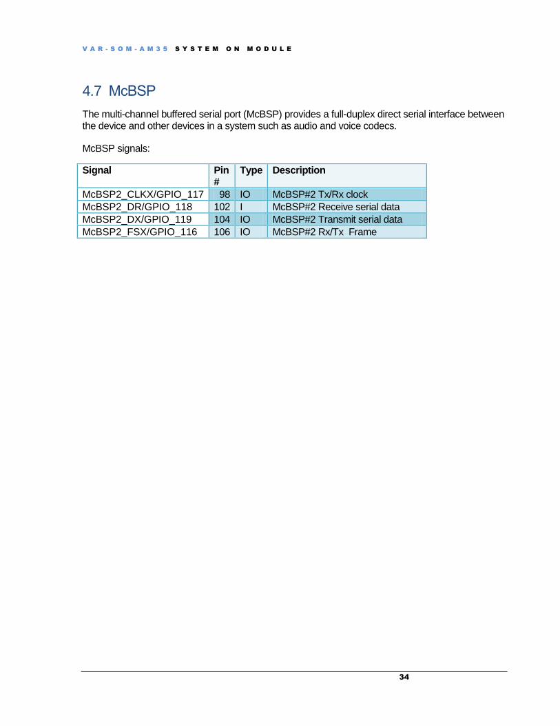
4.7 McBSP
The multi-channel buffered serial port (McBSP) provides a full-duplex direct serial interface between the device and other devices in a system such as audio and voice codecs.
McBSP signals:
Signal Pin #
Type Description
McBSP2_CLKX/GPIO_117 98 IO McBSP#2 Tx/Rx clock
McBSP2_DR/GPIO_118 102 I McBSP#2 Receive serial data
McBSP2_DX/GPIO_119 104 IO McBSP#2 Transmit serial data
McBSP2_FSX/GPIO_116 106 IO McBSP#2 Rx/Tx Frame

V A R - S O M - A M 3 5 S Y S T E M O N M O D U L E
35
4.8 SPI
The VAR-SOM-AM35 supports up to 3 SPI ports.
The McSPI ports supports the following main features:
Serial clock with programmable frequency, polarity, and phase for each channel
Wide selection of SPI word lengths ranging from 4 bits to 32 bits
Up to four master channels or single channel in slave mode
Master multichannel mode: - Full duplex/half duplex - Transmit-only/receive-only/transmit-and-receive modes - Flexible I/O port controls per channel - Two direct memory access (DMA) requests (read/write) per channel
Single interrupt line for multiple interrupt source events
Power management through wake-up capabilities
Enable the addition of a programmable start-bit for SPI transfer per channel (start-bit mode)
Support start-bit write command
Support start-bit pause and break sequence
64 bytes built-in FIFO available for a single channel
VAR-SOM-AM35 MsSPI signals:
Note: SPI2 and SPI3 signals are multiplexed with MMC1, MMC2 , or DSS_Data18 – DSS_Data signals
SPI2:
Signal Pin # Type Description
MCSPI2_CLK/MMC1_DAT0/GPIO_122 36 IO MsSPI2 Clock
MCSPI2_SIMO/MMC1_DAT1/GPIO_123 38 IO MsSPI2 SIMO Signal
MCSPI2_SOMI/MMC1_DAT2/GPIO_124 40 IO MsSPI2 SOMI Signal
MCSPI2_CS0/MMC1_DAT3/GPIO_125 42 IO MsSPI2 Chip-select 0 Signal

V A R - S O M - A M 3 5 S Y S T E M O N M O D U L E
36
SPI3:
4.9 I2C
The VAR-SOM-AM35 exposes 2 I2C ports:
VAR-SOM-AM35 I2C signals:
4.10 HDQ/1-Wire
The HDQ/1-Wire module implements the hardware protocol of the master functions of the Benchmark HDQ and the Dallas Semiconductor 1-Wire® protocols. These protocols use a single wire for communication between the master (HDQ/1-Wire controller) and the slave (HDQ/1-Wire external compliant device).
VAR-SOM-AM35 1-Wire / HDQ signals:
Signal Pin # Type Description
MCSPI3_SOMI/MMC2_DAT0/GPIO_132 168 IO MsSPI3 SOMI Signal
MCSPI3_SIMO/MMC2_CMD/GPIO_131 166 IO MsSPI3 SIMO Signal
MCSPI3_CS0/MMC2_DAT3/GPIO_135 174 IO MsSPI3 Chip-select 0 Signal
MCSPI3_CS1/MMC2_DAT2/GPIO_134 172 IO MsSPI3 Chip-select 1 Signal
MCSPI3_CLK/MMC2_CLK/GPIO_130 164 IO MsSPI3 Clock
LCD_D18/McSPI3_CLK/LCD_D4/GPIO88 20 IO MsSPI3 Clock
LCD_D19/McSPI3_SIMO/LCD_D3/GPIO89 19 IO MsSPI3 SIMO Signal
LCD_D20/McSPI3_SOMI/LCD_D2/GPIO90 22 IO MsSPI3 SOMI Signal
LCD_D21/McSPI3_CS0/LCD_D1/GPIO91 21 IO MsSPI3 Chip-select 0 Signal
LCD_D22/McSPI3_CS1/LCD_D0/GPIO92 24 IO MsSPI3 Chip-select 1 Signal
Signal Pin #
Type Description
I2C2_SDA/GPIO_168 99 IO I2C#2 SDA (data) internally pulled up to 3.3v
I2C2_SCL/GPIO_183 101 O I2C#2 SCL (clock) internally pulled up to 3.3v
I2C3_SDA/GPIO_185 61 IO I2C#3 SDA (data) requires external pull-up to 3.3v
I2C3_SCL/GPIO_184 63 O I2C#3 SCL (clock) requires external pull-up to 3.3v
Signal Pin # Type Description
HDQ/GPIO_170 82 IO HDQ / 1-Wire Line

V A R - S O M - A M 3 5 S Y S T E M O N M O D U L E
37
4.11 SD / MMC
The VAR-SOM-AM35 has two SD / MMC interfaces
The MMC/SD/SDIO host controllers deal with MMC/SD/SDIO protocol at transmission level, data packing, adding cyclic redundancy checks (CRC), start/end bit, and checking for syntactical correctness.
The application interface can send every MMC/SD/SDIO command and either poll for the status of the adapter or wait for an interrupt request, which is sent back in case of exceptions or to warn of end of operation.
The application interface can read card responses or flag registers. It can also mask individual interrupt sources. All these operations can be performed by reading and writing control registers. The MMC/SD/SDIO host controller also supports two DMA channels.
Note: SPI signals are multiplexed with MMC1 / MMC2 signals
MMC1 signals:
MMC2 signals:
Automatic Card detection not included in BSP
Signal Pin #
Type Description
MMC1_DAT0/GPIO_122 36 IO MMC#1 Data 0
MMC1_DAT1/GPIO_123 38 IO MMC#1 Data 1
MMC1_DAT2/GPIO_124 40 IO MMC#1 Data 2
MMC1_DAT3/GPIO_125 42 IO MMC#1 Data 3
MMC1_CLKO/GPIO_120 32 O MMC#1 Clock
MMC1_CMD/GPIO_121 43 IO MMC#1 Command
Signal Pin #
Type Description
MMC2_DAT0/GPIO_132 168 IO MMC2 Data 0
MMC2_DAT1/GPIO_133 170 IO MMC2 Data 1
MMC2_DAT2/GPIO_134 172 IO MMC2 Data 2
MMC2_DAT3/GPIO_135 174 IO MMC2 Data 3
MMC2_DAT4/GPIO_136 191 IO MMC2 Data 4
MMC2_DAT5/GPIO_137 193 IO MMC2 Data 5
MMC2_DAT6/GPIO_138 195 IO MMC2 Data 6
MMC2_DAT7/GPIO_139 199 IO MMC2 Data 7
MMC2_CLK/GPIO_130 164 IO MMC2 Clock
MMC2_CMD/GPIO_131 166 IO MMC2 CMD

V A R - S O M - A M 3 5 S Y S T E M O N M O D U L E
38
4.12 PWM
The VAR-SOM-AM35 provides a PWM signal:
PWM outputs from the OMAP processor (Not Supported by default BSP):
Signal Pin # Type Description
GPT9_PWM_EVT/GPIO_55 189 O pulse width modulation
Signal Pin # Type Description
LB_nCS3/GPIO_54 89 IO Local bus Chip select 3
UART2_CTS/GPIO_144 65 I UART#2 CTS
UART2_RTS/GPIO_145 67 O UART#2 RTS
UART2_RX/GPIO_147 71 I UART#2 RX
UART2_TX/GPIO_146 69 O UART#2 TX

V A R - S O M - A M 3 5 S Y S T E M O N M O D U L E
39
4.13 Local Bus
The general-purpose memory controller (GPMC) is used to interface external memory devices:
SRAMs
Asynchronous, synchronous, and page mode (only available in non-muxed mode) burst NOR flash devices
NAND flashes
Pseudo-SRAM devices
VAR-SOM-AM35 Local bus signals:
Signal Pin #
Type Description
LB_IO_0 149 IO Local bus data
LB_IO_1 147 IO Local bus data
LB_IO_2 145 IO Local bus data
LB_IO_3 143 IO Local bus data
LB_IO_4 141 IO Local bus data
LB_IO_5 139 IO Local bus data
LB_IO_6 137 IO Local bus data
LB_IO_7 135 IO Local bus data
LB_IO_8 133 IO Local bus data
LB_IO_9 131 IO Local bus data
LB_IO_10 129 IO Local bus data
LB_IO_11 132 IO Local bus data
LB_IO_12 138 IO Local bus data
LB_IO_13 140 IO Local bus data
LB_IO_14 134 IO Local bus data
LB_IO_15 136 IO Local bus data
LB_IO_A1/GPIO34 142 O Local bus address 1
LB_IO_A2/GPIO35 144 O Local bus address 2
LB_IO_A3/GPIO36 146 O Local bus address 3
LB_IO_A4/GPIO37 150 O Local bus address 4
LB_IO_A5/GPIO38 153 O Local bus address 5
LB_IO_A6/GPIO39 155 O Local bus address 6
LB_IO_A7/GPIO40 157 O Local bus address 7
LB_IO_A8/GPIO41 130 O Local bus address 8
LB_IO_A9/GPIO42 128 O Local bus address 9
LB_IO_A10/GPIO43 119 O Local bus address 10
LB_CLE 152 O Local bus Output enable for static memory, muxed with CLE
LB_CLK/GPIO_59 87 O Local Bus clock
LB_nADV_ALE 154 O Local bus Address Latch Enable, muxed with Address Valid
LB_nCS1/GPIO_52 52 O Local bus Chip Select 1

V A R - S O M - A M 3 5 S Y S T E M O N M O D U L E
40
Do not use Local bus IO signals as GPIOs, as those are internally used by on-board Nand flash
LB_nCS3/GPIO_54 89 O Local bus Chip Select 3
LB_RE_OE_N 125 O
Output enable (active low). Also used as read enable (active low) for NAND protocol memories.
LB_WE_N 160 O Local bus Write enable (active low)
SYS_nDMAREQ1/GPIO_65 85 I Local Bus SDMA Request 1
LB_WAIT1/GPIO63 148 I Local bus wait signal
V A R - S O M - A M 3 5 S Y S T E M O N M O D U L E
41
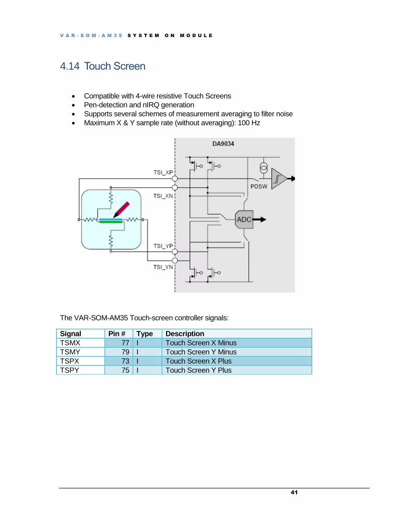
4.14 Touch Screen
Compatible with 4-wire resistive Touch Screens
Pen-detection and nIRQ generation
Supports several schemes of measurement averaging to filter noise
Maximum X & Y sample rate (without averaging): 100 Hz
The VAR-SOM-AM35 Touch-screen controller signals:
Signal Pin # Type Description
TSMX 77 I Touch Screen X Minus
TSMY 79 I Touch Screen Y Minus
TSPX 73 I Touch Screen X Plus
TSPY 75 I Touch Screen Y Plus

V A R - S O M - A M 3 5 S Y S T E M O N M O D U L E
42
4.15 JTAG
The VAR-SOM-AM35 has a dedicated JTAG connector.
Refer to CB105 extension board for required pull-up / pull-down resistors.
Signal Pin #
JTAG_TDO 1
JTAG_EMU1 2
JTAG_nTRST 3
JTAG_EMU0 4
JTAG_TMS 5
JTAG_RTCK 6
JTAG_TDI 7
NC 8
JTAG_TCK 9
GND 10

V A R - S O M - A M 3 5 S Y S T E M O N M O D U L E
43
4.16 Can Bus cotroller
The VAR-SOM-AM35 supports one CAN-Bus port.
The CAN controller is available in two different implementations that are both fully compliant with the CAN protocol, version 2.0B. The two different CAN controller versions use the same CAN protocol kernel module to perform the basic CAN protocol tasks. Only the message controller differs between the two CAN controller versions.
Key features of the CAN module include:
Common CAN protocol kernel (CPK) to perform protocol tasks
Standard CAN controller (SCC) for standard CAN applications
– Sixteen message-object acceptance-filtering
High-end CAN controller (HECC) for complex applications
– Thirty-two message objects full-mask acceptance-filtering
Refer to TI's AM3517 documentation for further information.
VAR-SOM-AM35 Can-Bus signals:
Signal Pin # Type Description
CAN_RX/GPIO_131 1 I CAN Bus RX
CAN_TX/GPIO_130 2 O CAN Bus TX

V A R - S O M - A M 3 5 S Y S T E M O N M O D U L E
44
4.17 Boot Option
The Boot option signal configures the boot sequence of the AM35xx processor. Use this signal to burn the Bootloader on NAND Flash.
VAR-SOM-AM35 boot signal:
SYS_BOOT pin configuration of SOM:
SYS_BOOT_PIN LOGIC STATE
SYS_BOOT_0 1
SYS_BOOT_1 1
SYS_BOOT_2 1
SYS_BOOT_3 1
SYS_BOOT_4 0
SYS_BOOT_5 Boot Select
SYS_BOOT_6 1
Signal Pin # Type Description
SYS_BOOT5 92 I System Boot Option 5 [High – Burn flash]
V A R - S O M - A M 3 5 S Y S T E M O N M O D U L E
45
4.18 General Purpose IOs
Most of the SOM' IO pins can be used as GPIOs.
See Chapter 3 for a complete SOM connector signal list and GPIO multiplexing.
The following pins can be used as GPIOs only.
4.19 General System signals
4.20 RTC
VAR-SOM-AM35 uses Intersil ISL12057 RTC IC, which keeps running as long as RTC_BACKUP is above 2.5v.
Signal Pin # Type Description
GPIO_153 176 IO GPIO_153
GPIO_157 185 IO GPIO_157
GPIO_128 34 IO GPIO_128
GPIO_129 30 IO GPIO_129
GPIO_142 177 IO GPIO_142
GPIO_143 175 IO GPIO_143
GPIO_156 183 IO GPIO_156
GPIO_160 187 IO GPIO_160
GPIO_61 91 IO GPIO_61
GPIO_126 27 IO GPIO_126
Signal Pin #
Type Description
RESET_IN_N 127 I Hardware Reset
RESET_OUT_N 97 O Reset Signal to Base-Board Peripherals
SYS_CLKOUT1/GPIO_10 49 O General Purpose Clock-out 1
SYS_CLKOUT2/GPIO186 109 IO General purpose Clock-out 2

V A R - S O M - A M 3 5 S Y S T E M O N M O D U L E
46
4.21 TV-OUT
Composite NTSC/PAL Video output.
4.22 Power supply pins
VAR-SOM-AM35 power supply pins:
VAR-SOM-AM35 Ground pins:
Signal Pin # Type Description
TV-OUT 54 O TV-OUT Analog signal out
Signal Pin # Type Description
VBAT 110,112,114,116 I VAR-SOM-AM35 single DC-IN supply voltage. Voltage range: 3.3 – 6V
VCC33A 169 O 3.3 V Output to Ethernet Magnetics
VIO 117 O 3.3v Output, up to 200ma
RTC_BACKUP 126 I RTC backup-battery power supply
Signal Pin # Type Description
GND 9,10,25,37,39,41,47,48,51,58,60,74,81,83,94,96,100,108,113,115,151,156,159,162,1
78,179,180,181,182,184,194,198,200

V A R - S O M - A M 3 5 S Y S T E M O N M O D U L E
47
5 Absolute maximum Characteristics Power supplies Min Max Unit
Main Power supply, DC-IN (VBAT) -0.3 6.5 V
VCC33A output supply 3.21 3.41 V
VCC33A output supply 200 ma
VIO 3.3v power output 3.23 3.41 V
VIO 3.3v power output 200 ma
6 Operational Characteristics 6.1 Supply voltages
Power supplies Min Max Unit
Main Power supply, DC-IN (VBAT) 3.3 6 V
RTC Backup battery voltage 2.5 3.2 V
6.2 VBAT power-on / power-off sequence
1. VBAT rise time should be lower than 3ms 2. If VBAT drops below 3.2v, VBAT should be powered off, and reach below 0.4v before power-on
again.
6.3 Typical power consumption
Power consumption:
Scenario Typical
3. CPU Load 30% 4. Ethernet controller operational 5. Power for Ethernet magnetics from
external source 6. Audio codec operational 7. One USB host phy
1.2Watt
8. CPU Load 80% 9. Ethernet controller operational 10. Power for Ethernet magnetics from
SOM 11. Audio codec operational 12. Two USB host phys
1.8Watt

V A R - S O M - A M 3 5 S Y S T E M O N M O D U L E
48
7 DC electrical characteristics Parameter Operating Conditions Min Typ Max Unit
3.3v Digital IO (UARTs, LCD, MMC2,MMC1, ISP, SPI, McBSP, I2C,Local Bus, JTAG)
VIH
2.1 3.4 V
VIL -0.2 0.8 V
VOH
3.0 3.3 V
VOL
0.2 0.4 V
When main power supply (VIN) is 3.3v. 3.3v Digital IO outputs are VIN-50mV
8 Environmental specifications
Min Max
Commercial operating temperature range 00C +70
0C
Extended operating temperature range -250C +70
0C
Industrial operating temperature range -400C +85
0C
Variscite uses MIL-HDBK-217F-2 Parts count reliability prediction method Model:
50Deg Celsius, Class B-1, GM 50Deg Celsius, Class B-1, GB
121 Khrs > 1400 Khrs >
Shock resistance 50G / 20 ms
Vibration 20G / 0 - 600 Hz
V A R - S O M - A M 3 5 S Y S T E M O N M O D U L E
49
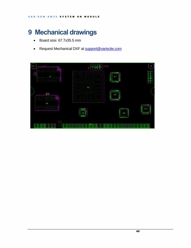
9 Mechanical drawings Board size: 67.7x35.5 mm
Request Mechanical DXF at [email protected]

V A R - S O M - A M 3 5 S Y S T E M O N M O D U L E
50
10 Legal notice Variscite LTD (“Variscite”) products and services are sold subject to Variscite’s terms and conditions of sale, delivery and payment supplied at the time of order acknowledgement.
Variscite warrants performance of its products to the specifications in effect at the date of shipment. Variscite reserves the right to make changes to its products and specifications or to discontinue any product or service without notice. Customers should therefore obtain the latest version of relevant information from Variscite to verify that the information is current.
Testing and other quality control techniques are utilized to the extent Variscite deems necessary to support its warranty.
Specific testing of all parameters of each device is not necessarily performed unless required by law or regulation.
In order to minimize risks associated with customer applications, the customer must use adequate design and operating safeguards to minimize inherent or procedural hazards. Variscite is not liable for applications assistance or customer product design. The customer is solely responsible for its selection and use of Variscite products. Variscite is not liable for such selection or use nor for use of any circuitry other than circuitry entirely embodied in a Variscite product.
Variscite products are not intended for use in life support systems, appliances, nuclear systems or systems where malfunction can reasonably be expected to result in personal injury, death or severe property or environmental damage. Any use of products by the customer for such purposes is at the customer’s own risk.
Variscite does not grant any license (express or implied) under any patent right, copyright, mask work right or other intellectual property right of Variscite covering or relating to any combination, machine, or process in which its products or services might be or are used. Any provision or publication of any third party’s products or services does not constitute Variscite’s approval, license, warranty or endorsement thereof. Any third party trademarks contained in this document belong to the respective third party owner.
Reproduction of information from Variscite datasheets is permissible only if reproduction is without alteration and is accompanied by all associated copyright, proprietary and other notices (including this notice) and conditions. Variscite is not liable for any un-authorized alteration of such information or for any reliance placed thereon.
Any representations made, warranties given, and/or liabilities accepted by any person which differ from those contained in this datasheet or in Variscite’s standard terms and conditions of sale, delivery and payment are made, given and/or accepted at that person’s own risk. Variscite is not liable for any such representations, warranties or liabilities or for any reliance placed thereon by any person.

V A R - S O M - A M 3 5 S Y S T E M O N M O D U L E
51
11 Warranty terms
Variscite guarantees hardware products against defects in workmanship and material for a period of one (1) year from the date of shipment. Your sole remedy and Variscite’s sole liability shall be for Variscite, at its sole discretion, to either repair or replace the defective hardware product at no charge or to refund the purchase price. Shipment costs in both directions are the responsibility of the customer. This warranty is void if the hardware product has been altered or damaged by accident, misuse or abuse.
Disclaimer of Warranty
THIS WARRANTY IS MADE IN LIEU OF ANY OTHER WARRANTY, WHETHER EXPRESSED, OR IMPLIED, OF MERCHANTABILITY, FITNESS FOR A SPECIFIC PURPOSE, NON-INFRINGEMENT OR THEIR EQUIVALENTS UNDER THE LAWS OF ANY JURISDICTION, EXCEPT THE WARRANTY EXPRESSLY STATED HEREIN. THE REMEDIES SET FORTH HEREIN SHALL BE THE SOLE AND EXCLUSIVE REMEDIES OF ANY PURCHASER WITH RESPECT TO ANY DEFECTIVE PRODUCT.
Limitation on Liability
UNDER NO CIRCUMSTANCES SHALL VARISCITE BE LIABLE FOR ANY LOSS, DAMAGE OR EXPENSE SUFFERED OR INCURRED WITH RESPECT TO ANY DEFECTIVE PRODUCT. IN NO EVENT SHALL VARISCITE BE LIABLE FOR ANY INCIDENTAL OR CONSEQUENTIAL DAMAGES THAT YOU MAY SUFFER DIRECTLY OR INDIRECTLY FROM USE OF ANY PRODUCT.
V A R - S O M - A M 3 5 S Y S T E M O N M O D U L E
52
12 Contact information
Headquarters: Variscite LTD 60 Medinat Hayehudim st. P.O.B 12598 46722, Israel Tel: +972 (9) 9562910 Fax: +972 (9) 9589477
Sales: [email protected]
Technical support: [email protected]
Website: www.variscite.com