Embed Size (px)
Citation preview
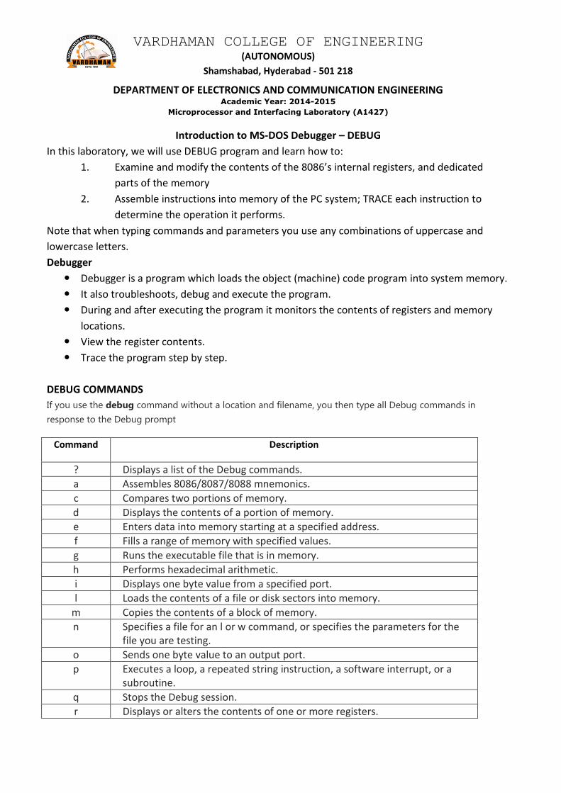
VARDHAMAN COLLEGE OF ENGINEERING (AUTONOMOUS)
Shamshabad, Hyderabad - 501 218
DEPARTMENT OF ELECTRONICS AND COMMUNICATION ENGINEERING Academic Year: 2014-2015
Microprocessor and Interfacing Laboratory (A1427)
Introduction to MS-DOS Debugger – DEBUG
In this laboratory, we will use DEBUG program and learn how to:
1. Examine and modify the contents of the 8086’s internal registers, and dedicated
parts of the memory
2. Assemble instructions into memory of the PC system; TRACE each instruction to
determine the operation it performs.
Note that when typing commands and parameters you use any combinations of uppercase and
lowercase letters.
Debugger
Debugger is a program which loads the object (machine) code program into system memory.
It also troubleshoots, debug and execute the program.
During and after executing the program it monitors the contents of registers and memory
locations.
View the register contents.
Trace the program step by step.
DEBUG COMMANDS
If you use the debug command without a location and filename, you then type all Debug commands in
response to the Debug prompt
Command Description
? Displays a list of the Debug commands.
a Assembles 8086/8087/8088 mnemonics.
c Compares two portions of memory.
d Displays the contents of a portion of memory.
e Enters data into memory starting at a specified address.
f Fills a range of memory with specified values.
g Runs the executable file that is in memory.
h Performs hexadecimal arithmetic.
i Displays one byte value from a specified port.
l Loads the contents of a file or disk sectors into memory.
m Copies the contents of a block of memory.
n Specifies a file for an l or w command, or specifies the parameters for the file you are testing.
o Sends one byte value to an output port.
p Executes a loop, a repeated string instruction, a software interrupt, or a subroutine.
q Stops the Debug session.
r Displays or alters the contents of one or more registers.
VARDHAMAN COLLEGE OF ENGINEERING (AUTONOMOUS)
Shamshabad, Hyderabad - 501 218
DEPARTMENT OF ELECTRONICS AND COMMUNICATION ENGINEERING Academic Year: 2014-2015
Microprocessor and Interfacing Laboratory (A1427)
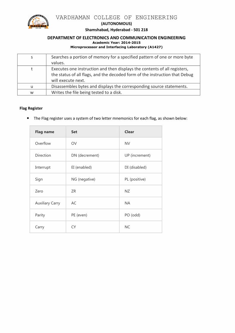
s Searches a portion of memory for a specified pattern of one or more byte values.
t Executes one instruction and then displays the contents of all registers, the status of all flags, and the decoded form of the instruction that Debug will execute next.
u Disassembles bytes and displays the corresponding source statements.
w Writes the file being tested to a disk.
Flag Register
The Flag register uses a system of two letter mnemonics for each flag, as shown below:
Flag name Set Clear
Overflow OV NV
Direction DN (decrement) UP (increment)
Interrupt EI (enabled) DI (disabled)
Sign NG (negative) PL (positive)
Zero ZR NZ
Auxiliary Carry AC NA
Parity PE (even) PO (odd)
Carry CY NC
VARDHAMAN COLLEGE OF ENGINEERING (AUTONOMOUS)
Shamshabad, Hyderabad - 501 218
DEPARTMENT OF ELECTRONICS AND COMMUNICATION ENGINEERING Academic Year: 2014-2015
Microprocessor and Interfacing Laboratory (A1427)
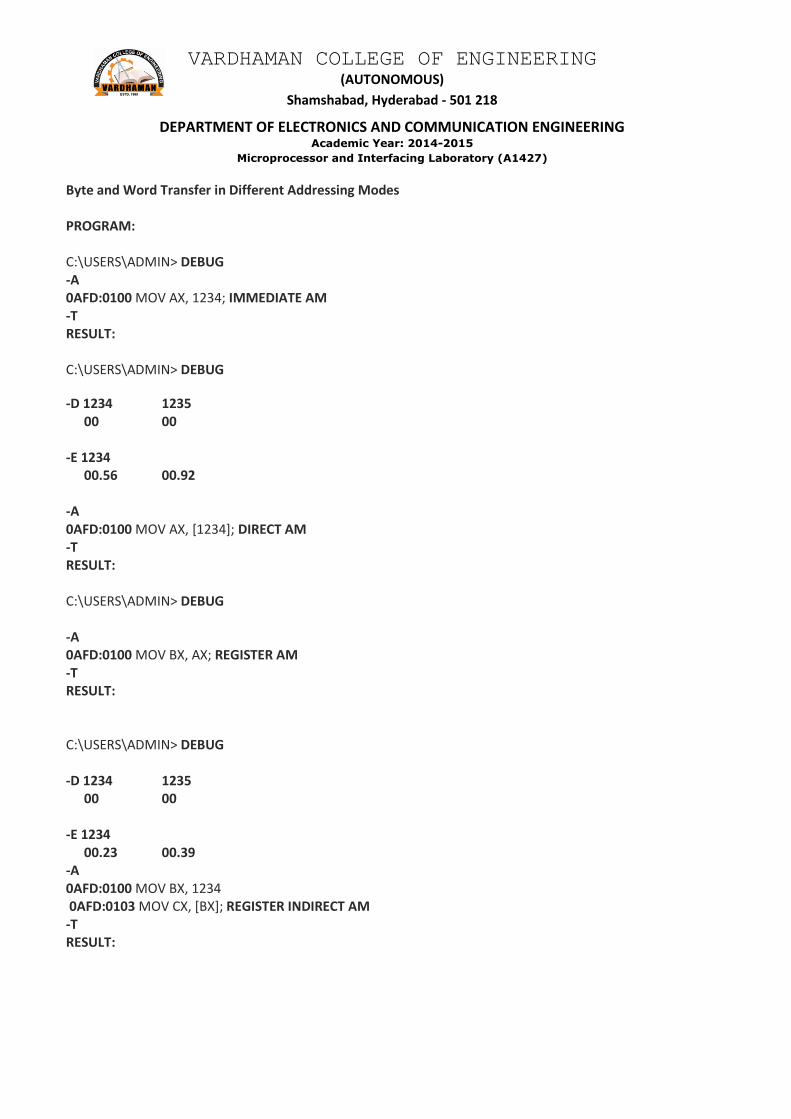
Byte and Word Transfer in Different Addressing Modes PROGRAM: C:\USERS\ADMIN> DEBUG -A 0AFD:0100 MOV AX, 1234; IMMEDIATE AM -T RESULT: C:\USERS\ADMIN> DEBUG
-D 1234 1235 00 00
-E 1234
00.56 00.92
-A 0AFD:0100 MOV AX, [1234]; DIRECT AM -T RESULT: C:\USERS\ADMIN> DEBUG -A 0AFD:0100 MOV BX, AX; REGISTER AM -T RESULT: C:\USERS\ADMIN> DEBUG -D 1234 1235
00 00 -E 1234
00.23 00.39 -A 0AFD:0100 MOV BX, 1234 0AFD:0103 MOV CX, [BX]; REGISTER INDIRECT AM -T RESULT:
VARDHAMAN COLLEGE OF ENGINEERING (AUTONOMOUS)
Shamshabad, Hyderabad - 501 218
DEPARTMENT OF ELECTRONICS AND COMMUNICATION ENGINEERING Academic Year: 2014-2015
Microprocessor and Interfacing Laboratory (A1427)
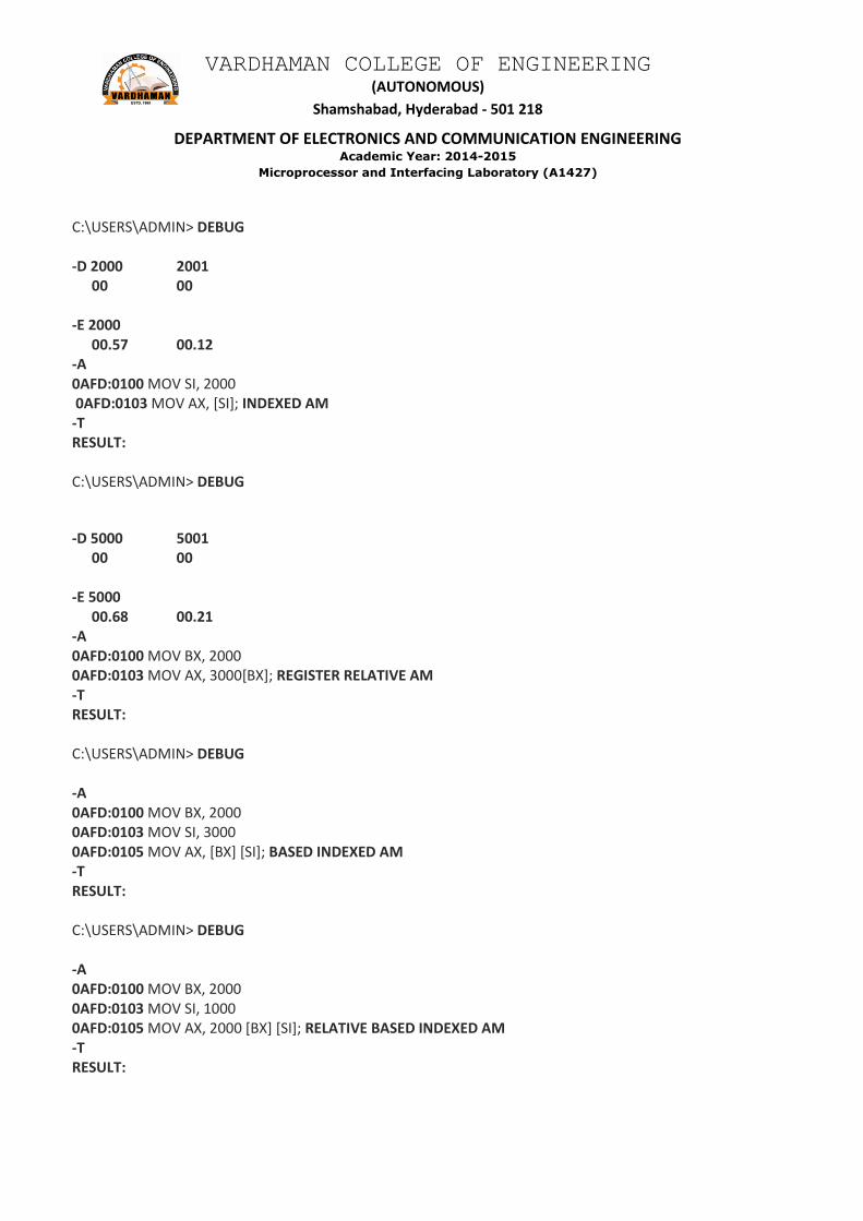
C:\USERS\ADMIN> DEBUG -D 2000 2001
00 00 -E 2000
00.57 00.12 -A 0AFD:0100 MOV SI, 2000 0AFD:0103 MOV AX, [SI]; INDEXED AM -T RESULT: C:\USERS\ADMIN> DEBUG
-D 5000 5001
00 00 -E 5000
00.68 00.21 -A 0AFD:0100 MOV BX, 2000 0AFD:0103 MOV AX, 3000[BX]; REGISTER RELATIVE AM -T RESULT: C:\USERS\ADMIN> DEBUG -A 0AFD:0100 MOV BX, 2000 0AFD:0103 MOV SI, 3000 0AFD:0105 MOV AX, [BX] [SI]; BASED INDEXED AM -T RESULT: C:\USERS\ADMIN> DEBUG -A 0AFD:0100 MOV BX, 2000 0AFD:0103 MOV SI, 1000 0AFD:0105 MOV AX, 2000 [BX] [SI]; RELATIVE BASED INDEXED AM -T RESULT:
VARDHAMAN COLLEGE OF ENGINEERING (AUTONOMOUS)
Shamshabad, Hyderabad - 501 218
DEPARTMENT OF ELECTRONICS AND COMMUNICATION ENGINEERING Academic Year: 2014-2015
Microprocessor and Interfacing Laboratory (A1427)
MASM 6.11(Microsoft Macro Assembler)
EDITOR
An editor is a program, which allows you to create a file containing the assembly language
statements for your program. As you type in your program, the editor stores the ASCII codes for
the letters and numbers in successive RAM locations. When you have typed in all of your
programs, you then save the file on a floppy of hard disk. This file is called source file. The next
step is to process the source file with an assembler. In the MASM assembler, you should give
your source file name the extension, .ASM
ASSEMBLER
An assembler program is used to translate the assembly language mnemonics for
instructions to the corresponding binary codes. When you run the assembler, it reads the source
file of your program the disk, where you saved it after editing on the first pass through the
source program the assembler determines the displacement of named data items, the offset of
labels and pails this information in a symbol table. On the second pass through the source
program, the assembler produces the binary code for each instruction and inserts the offset etc
that is calculated during the first pass. The assembler generates two files on floppy or hard disk.
The first file called the object file is given the extension .OBJ. The object file contains the binary
codes for the instructions and information about the addresses of the instructions. The second
file generated by the assembler is called assembler list file. The list file contains your assembly
language statements, the binary codes for each instructions and the offset for each instruction.
In MASM assembler, MASM source file name .ASM is used to assemble the file. Edit source file
name LST is used to view the list file, which is generated, when you assemble the file.
LINKER
A linker is a program used to join several object files into one large object file and convert to an
exe file. The linker produces a link file, which contains the binary codes for all the combined
modules. The linker however doesn’t assign absolute addresses to the program, it assigns is said
to be relocatable because it can be put anywhere in memory to be run. In MASM, LINK source
filename .OBJ is used to link the file.
DEBUGGER
A debugger is a program which allows you to load your object code program into system
memory, execute the program and troubleshoot are debug it the debugger allows you to look at
the contents of registers and memory locations after your program runs. It allows you to change
the contents of register and memory locations after your program runs. It allows you to change
VARDHAMAN COLLEGE OF ENGINEERING (AUTONOMOUS)
Shamshabad, Hyderabad - 501 218
DEPARTMENT OF ELECTRONICS AND COMMUNICATION ENGINEERING Academic Year: 2014-2015
Microprocessor and Interfacing Laboratory (A1427)
the contents of register and memory locations and return the program. A debugger also allows
you to set a break point at any point in the program. If you inset a breakpoint the debugger will
run the program up to the instruction where the breakpoint is set and stop execution. You can
then examine register and memory contents to see whether the results are correct at that point.
In MASM, DEBUG filename .EXE is issued to debug the file.
DEBUGGER FUNCTIONS:
1. Debugger allows looking at the contents of registers and memory locations.
2. We can extend 8-bit register to 16-bit register which the help of extended register option.
3. Debugger allows setting breakpoints at any point with the program.
4. The debugger will run the program up to the instruction where the breakpoint is set and then
stop execution of program. At this point, we can examine registry and memory contents at that
point.
Commands to Create and Execute a given ALP:
1. Creating: EDIT <FILENAME> .ASM 2. Assembling: MASM <FILENAME> .ASM 3. Linking: LINK <FILENAME> .OBJ 4. Debugging: DEBUG <FILENAME> .EXE
VARDHAMAN COLLEGE OF ENGINEERING (AUTONOMOUS)
Shamshabad, Hyderabad - 501 218
DEPARTMENT OF ELECTRONICS AND COMMUNICATION ENGINEERING Academic Year: 2014-2015
Microprocessor and Interfacing Laboratory (A1427)
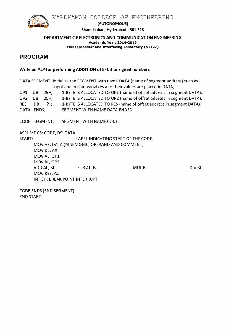
PROGRAM Write an ALP for performing ADDITION of 8- bit unsigned numbers DATA SEGMENT; initialize the SEGMENT with name DATA (name of segment address) such as
input and output variables and their values are placed in DATA; OP1 DB 25H; 1-BYTE IS ALLOCATED TO OP1 (name of offset address in segment DATA). OP2 DB 20H; 1-BYTE IS ALLOCATED TO OP2 (name of offset address in segment DATA). RES DB ? ; 1-BYTE IS ALLOCATED TO RES (name of offset address in segment DATA). DATA ENDS; SEGMENT WITH NAME DATA ENDED CODE SEGMENT; SEGMENT WITH NAME CODE ASSUME CS: CODE, DS: DATA START: LABEL INDICATING START OF THE CODE. MOV AX, DATA (MNEMONIC, OPERAND AND COMMENT). MOV DS, AX MOV AL, OP1 MOV BL, OP2 ADD AL, BL SUB AL, BL MUL BL DIV BL MOV RES, AL INT 3H; BREAK POINT INTERRUPT CODE ENDS (END SEGMENT) END START
VARDHAMAN COLLEGE OF ENGINEERING (AUTONOMOUS)
Shamshabad, Hyderabad - 501 218
DEPARTMENT OF ELECTRONICS AND COMMUNICATION ENGINEERING Academic Year: 2014-2015
Microprocessor and Interfacing Laboratory (A1427)
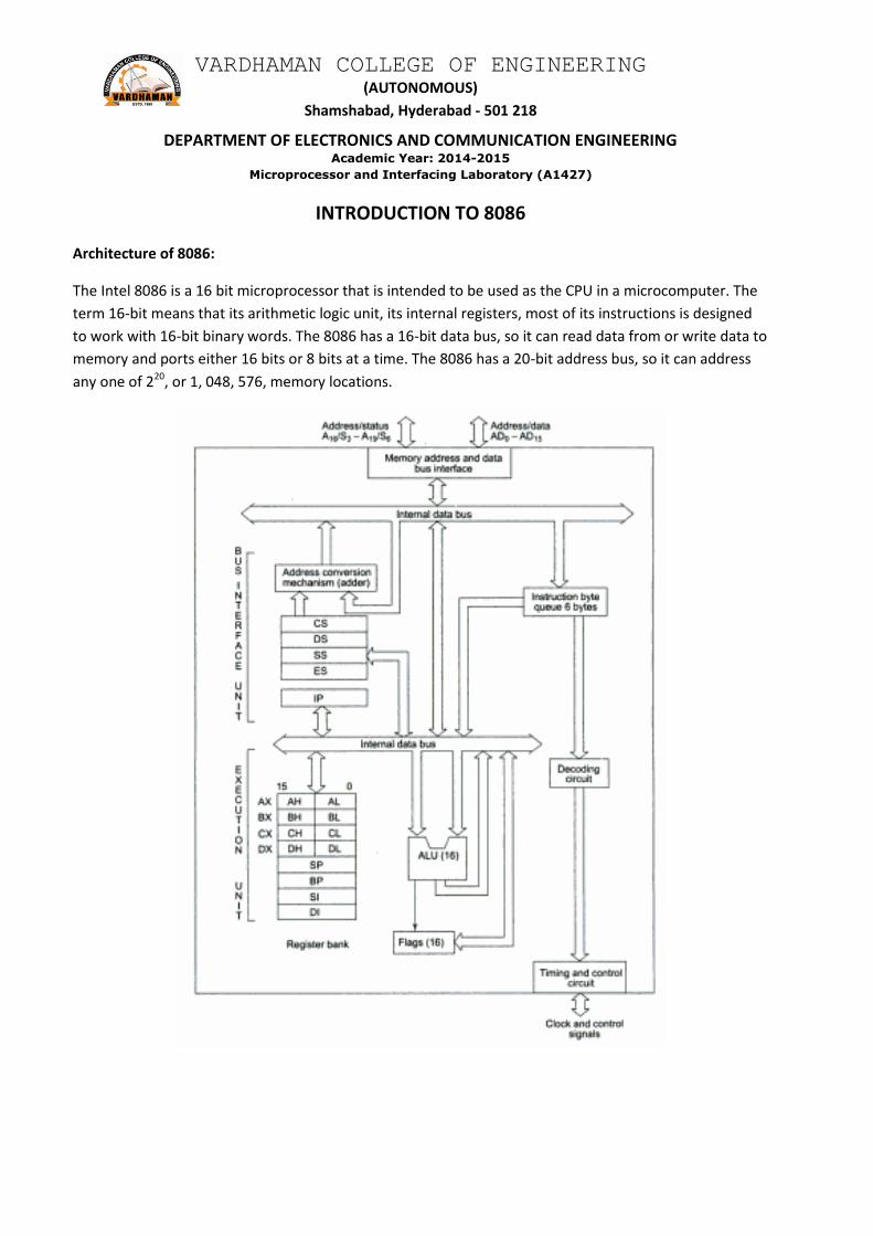
INTRODUCTION TO 8086
Architecture of 8086:
The Intel 8086 is a 16 bit microprocessor that is intended to be used as the CPU in a microcomputer. The
term 16-bit means that its arithmetic logic unit, its internal registers, most of its instructions is designed
to work with 16-bit binary words. The 8086 has a 16-bit data bus, so it can read data from or write data to
memory and ports either 16 bits or 8 bits at a time. The 8086 has a 20-bit address bus, so it can address
any one of 220, or 1, 048, 576, memory locations.
VARDHAMAN COLLEGE OF ENGINEERING (AUTONOMOUS)
Shamshabad, Hyderabad - 501 218
DEPARTMENT OF ELECTRONICS AND COMMUNICATION ENGINEERING Academic Year: 2014-2015
Microprocessor and Interfacing Laboratory (A1427)
The 8086 CPU is divided into two independent functional parts, the bus interface unit (BIU), and the
execution unit (EU). Dividing the work between these two units speeds up processing.
The BIU sends out addresses, fetches instructions from memory, reads data from ports and memory, and
writes data to ports and memory. BIU handles all transfers of data and addresses on the buses for the
execution unit. The bus interface unit contains the circuit for physical address calculations and a
predecoding instruction byte queue. The BIU makes the system’s bus signals available for external
interfacing of the devices.
Queue: while the EU is decoding an instruction or executing an instruction which does not require use of
the buses, the BIU fetches up to six instruction bytes for the following instructions. The BIU stores these
pre-fetched bytes in a first-in-first out register set called queue. When EU is ready for its next instruction,
it simply reads the instruction byte for the instruction from the queue in the BIU. This is much faster than
sending out an address to the system memory and waiting for memory to send back the next instruction
byte. The six byte long queue was chosen because the maximum number of bytes required for any
instruction in 8086 is this long.
The execution unit tells the BIU where to fetch instructions or data from, decodes instructions and
executes instructions. The EU contains the register set of 8086 except segment registers and IP. It has a
16-bit ALU to perform air thematic and logical operations, the 16-bit flag register reflect the results of
execution by ALU. The decoding unit decodes the opcode bytes issued from the instruction byte queue.
The timing and control unit derives the necessary control signals to execute the instruction opcode
received from the queue, depending upon the information made available by the decoding circuit. The
execution unit may pass the results to the BIU for storing them in memory.
Register Organization
8086 has a powerful set of registers known as general purpose and special purpose registers. All the
registers are of 16 bit. The general purpose registers, can be used as either 8-bit registers or 16-bit
registers. They may be either used for holding data, variables and intermediate results temporarily or for
other purpose like counter or for storing offset address for some addressing modes etc. the special
purpose registers are used as segment registers, pointers, index registers or as offset storage registers for
particular addressing modes.
The 8086 registers are classified into the following types:
1. General Purpose Data Registers(AX, BX, CX, DX)
2. Segment Registers(CS, DS, ES, SS)
3. Pointers and Index Registers(IP, BP, SP, SI, DI)
4. Flag Registers(S,Z,P,C,T,I,D,AC,O)
VARDHAMAN COLLEGE OF ENGINEERING (AUTONOMOUS)
Shamshabad, Hyderabad - 501 218
DEPARTMENT OF ELECTRONICS AND COMMUNICATION ENGINEERING Academic Year: 2014-2015
Microprocessor and Interfacing Laboratory (A1427)
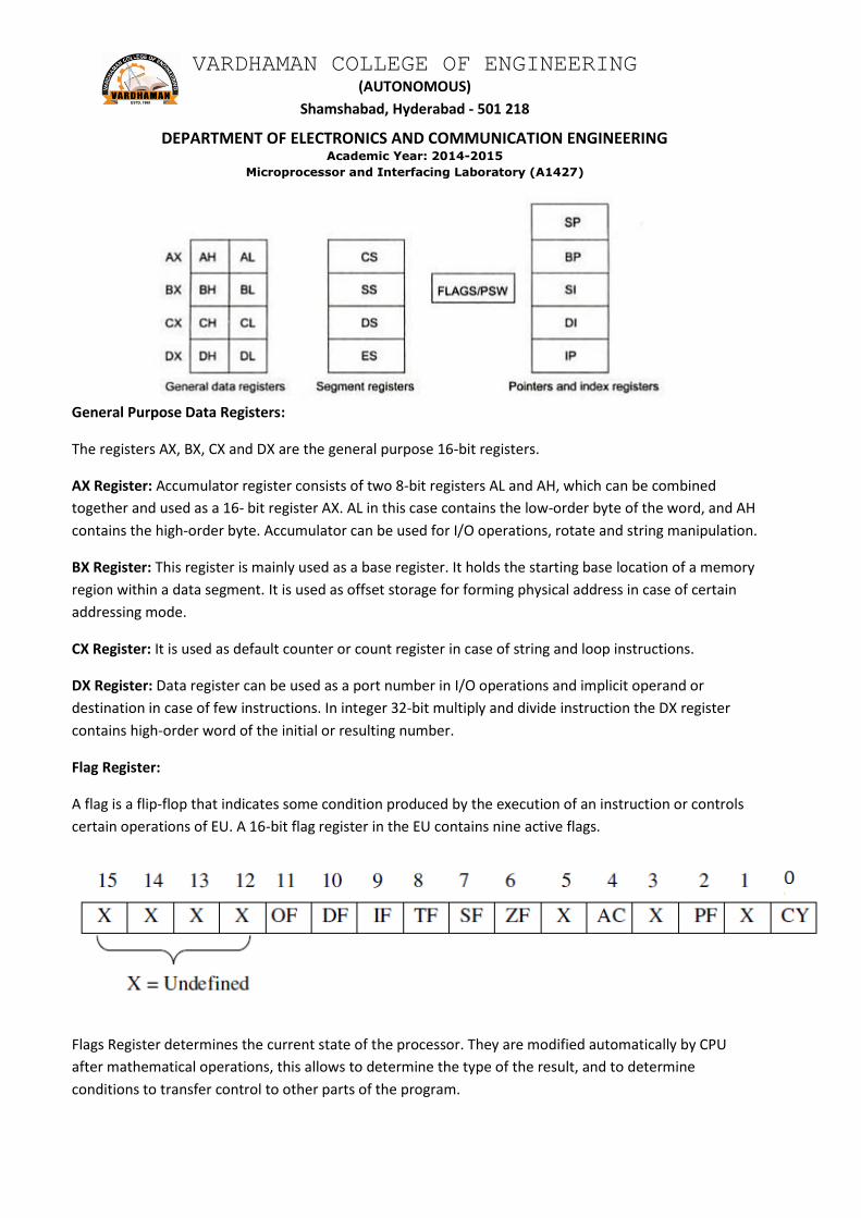
General Purpose Data Registers:
The registers AX, BX, CX and DX are the general purpose 16-bit registers.
AX Register: Accumulator register consists of two 8-bit registers AL and AH, which can be combined
together and used as a 16- bit register AX. AL in this case contains the low-order byte of the word, and AH
contains the high-order byte. Accumulator can be used for I/O operations, rotate and string manipulation.
BX Register: This register is mainly used as a base register. It holds the starting base location of a memory
region within a data segment. It is used as offset storage for forming physical address in case of certain
addressing mode.
CX Register: It is used as default counter or count register in case of string and loop instructions.
DX Register: Data register can be used as a port number in I/O operations and implicit operand or
destination in case of few instructions. In integer 32-bit multiply and divide instruction the DX register
contains high-order word of the initial or resulting number.
Flag Register:
A flag is a flip-flop that indicates some condition produced by the execution of an instruction or controls
certain operations of EU. A 16-bit flag register in the EU contains nine active flags.
Flags Register determines the current state of the processor. They are modified automatically by CPU
after mathematical operations, this allows to determine the type of the result, and to determine
conditions to transfer control to other parts of the program.
VARDHAMAN COLLEGE OF ENGINEERING (AUTONOMOUS)
Shamshabad, Hyderabad - 501 218
DEPARTMENT OF ELECTRONICS AND COMMUNICATION ENGINEERING Academic Year: 2014-2015
Microprocessor and Interfacing Laboratory (A1427)
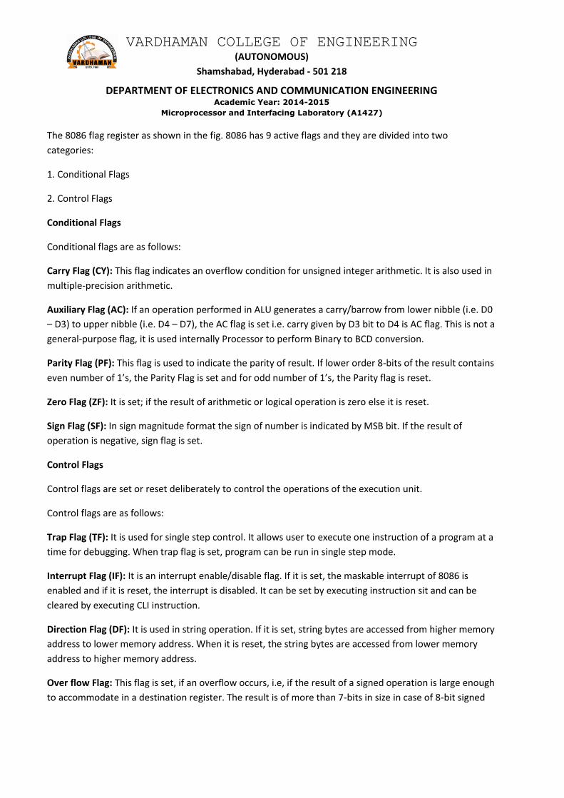
The 8086 flag register as shown in the fig. 8086 has 9 active flags and they are divided into two
categories:
1. Conditional Flags
2. Control Flags
Conditional Flags
Conditional flags are as follows:
Carry Flag (CY): This flag indicates an overflow condition for unsigned integer arithmetic. It is also used in
multiple-precision arithmetic.
Auxiliary Flag (AC): If an operation performed in ALU generates a carry/barrow from lower nibble (i.e. D0
– D3) to upper nibble (i.e. D4 – D7), the AC flag is set i.e. carry given by D3 bit to D4 is AC flag. This is not a
general-purpose flag, it is used internally Processor to perform Binary to BCD conversion.
Parity Flag (PF): This flag is used to indicate the parity of result. If lower order 8-bits of the result contains
even number of 1’s, the Parity Flag is set and for odd number of 1’s, the Parity flag is reset.
Zero Flag (ZF): It is set; if the result of arithmetic or logical operation is zero else it is reset.
Sign Flag (SF): In sign magnitude format the sign of number is indicated by MSB bit. If the result of
operation is negative, sign flag is set.
Control Flags
Control flags are set or reset deliberately to control the operations of the execution unit.
Control flags are as follows:
Trap Flag (TF): It is used for single step control. It allows user to execute one instruction of a program at a
time for debugging. When trap flag is set, program can be run in single step mode.
Interrupt Flag (IF): It is an interrupt enable/disable flag. If it is set, the maskable interrupt of 8086 is
enabled and if it is reset, the interrupt is disabled. It can be set by executing instruction sit and can be
cleared by executing CLI instruction.
Direction Flag (DF): It is used in string operation. If it is set, string bytes are accessed from higher memory
address to lower memory address. When it is reset, the string bytes are accessed from lower memory
address to higher memory address.
Over flow Flag: This flag is set, if an overflow occurs, i.e, if the result of a signed operation is large enough
to accommodate in a destination register. The result is of more than 7-bits in size in case of 8-bit signed
VARDHAMAN COLLEGE OF ENGINEERING (AUTONOMOUS)
Shamshabad, Hyderabad - 501 218
DEPARTMENT OF ELECTRONICS AND COMMUNICATION ENGINEERING Academic Year: 2014-2015
Microprocessor and Interfacing Laboratory (A1427)
operation and more than 15-bits in size in case of 16-bit sign operations, and then the overflow will be
set.
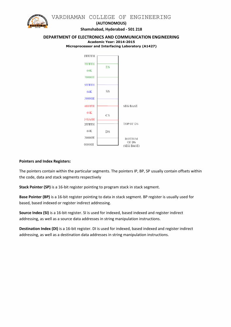
Segment Registers:
To complete 1Mbyte memory is divided into 16 logical segments. The complete 1Mbyte memory
segmentation is as shown in fig 1.5. Each segment contains 64Kbyte of memory. There are four segment
registers.
Code segment (CS) is a 16-bit register containing address of 64 KB segment with processor instructions.
The processor uses CS segment for all accesses to instructions referenced by instruction pointer (IP)
register. CS register cannot be changed directly. The CS register is automatically updated during far jump,
far call and far return instructions. It is used for addressing a memory location in the code segment of the
memory, where the executable program is stored.
Stack segment (SS) is a 16-bit register containing address of 64KB segment with program stack. By
default, the processor assumes that all data referenced by the stack pointer (SP) and base pointer (BP)
registers is located in the stack segment. SS register can be changed directly using POP instruction. It is
used for addressing stack segment of memory. The stack segment is that segment of memory, which is
used to store stack data.
Data segment (DS) is a 16-bit register containing address of 64KB segment with program data. By default,
the processor assumes that all data referenced by general registers (AX, BX, CX, DX) and index register (SI,
DI) is located in the data segment. DS register can be changed directly using POP and LDS instructions. It
points to the data segment memory where the data is resided.
Extra segment (ES) is a 16-bit register containing address of 64KB segment, usually with program data. By
default, the processor assumes that the DI register references the ES segment in string manipulation
instructions. ES register can be changed directly using POP and LES instructions. It also refers to segment
which essentially is another data segment of the memory. It also contains data.
VARDHAMAN COLLEGE OF ENGINEERING (AUTONOMOUS)
Shamshabad, Hyderabad - 501 218
DEPARTMENT OF ELECTRONICS AND COMMUNICATION ENGINEERING Academic Year: 2014-2015
Microprocessor and Interfacing Laboratory (A1427)
Pointers and Index Registers:
The pointers contain within the particular segments. The pointers IP, BP, SP usually contain offsets within
the code, data and stack segments respectively
Stack Pointer (SP) is a 16-bit register pointing to program stack in stack segment.
Base Pointer (BP) is a 16-bit register pointing to data in stack segment. BP register is usually used for
based, based indexed or register indirect addressing.
Source Index (SI) is a 16-bit register. SI is used for indexed, based indexed and register indirect
addressing, as well as a source data addresses in string manipulation instructions.
Destination Index (DI) is a 16-bit register. DI is used for indexed, based indexed and register indirect
addressing, as well as a destination data addresses in string manipulation instructions.
VARDHAMAN COLLEGE OF ENGINEERING (AUTONOMOUS)
Shamshabad, Hyderabad - 501 218
DEPARTMENT OF ELECTRONICS AND COMMUNICATION ENGINEERING Academic Year: 2014-2015
Microprocessor and Interfacing Laboratory (A1427)
Addressing Modes of 8086:
Addressing mode indicates a way of locating data or operands.
The addressing modes describe the types of operands and the way they are accessed for executing an instruction.
According to the flow of instruction execution, the instructions may be categorized as i) Sequential control flow instructions and ii) Control transfer instructions
Sequential control flow instructions are the instructions, which after execution, transfer control to the next instruction appearing immediately after it (in the sequence) in the program. For example, the arithmetic, logic, data transfer and processor control instructions are sequential control flow instructions.
The control transfer instructions, on the other hand, transfer control to same predefined address or the address somehow specified in the instruction, after their execution. For example, INT, CALL, RET and JUMP instructions fall under this category.
The addressing modes for sequential control transfer instructions are:
1. Immediate: In this type of addressing, immediate data is a part of instruction and appears in the form of successive byte or bytes.
Ex: MOV AX, 0005H
In the above example, 0005H is the immediate data. The immediate data may be 8-bit or 16-bit in size.
2. Direct: In the direct addressing mode a 16-bit memory address (offset) is directly specified in the instruction as a part of it.
Ex: MOV AX, [5000H]
Here, data resides in a memory location in the data segment, whose effective address may be completed using 5000H as the offset address and content of DS as segment address. The effective address here, is 10H * DS + 5000H.
3. Register: In register addressing mode, the data is stored in a register and is referred using the particular register. All the registers, except IP, may be used in this mode.
Ex: MOV BX, AX
4. Register Indirect: Sometimes, the address of the memory location, which contains data or operand, is determined in an indirect way, using the offset register. This mode of addressing is known as register indirect mode. In this addressing mode, the offset address of data is in either BX or SI or DI registers. The default segment is either DS or ES. The data is supposed to be available at the address pointed to by the content of any of the above registers in the default data segment.
Ex: MOV AX, [BX]
Here, data is present in a memory location in DS whose offset address is in BX. The effective address of the data is given as 10H * DS+ [BX].
VARDHAMAN COLLEGE OF ENGINEERING (AUTONOMOUS)
Shamshabad, Hyderabad - 501 218
DEPARTMENT OF ELECTRONICS AND COMMUNICATION ENGINEERING Academic Year: 2014-2015
Microprocessor and Interfacing Laboratory (A1427)
5. Indexed: In this addressing mode, offset of the operand is stored in one of the index registers. DS and ES are the default segments for index registers, SI and DI respectively. This is a special case of register indirect addressing mode.
Ex: MOV AX, [SI]
Here, data is available at an offset address stored in SI in DS. The effective address, in this case, is computed as 10*DS+[SI].
6. Register Relative: In this addressing mode, the data is available at an effective address formed by adding an 8-bit or 16-bit displacement with the content of any one of the registers BX, BP, SI and DI in the default (either DS or ES) segment.
Ex: MOV AX, 50H [BX]
Here, the effective address is given as 10H *DS+50H+ [BX]
7. Based Indexed: The effective address of data is formed, in this addressing mode, by adding content of a base register (any one of BX or BP) to the content of an index register (any one of SI or DI). The default segment register may be ES or DS.
Ex: MOV AX, [BX][SI]
Here, BX is the base register and SI is the index register the effective address is computed as 10H * DS + [BX] + [SI].
8. Relative Based Indexed: The effective address is formed by adding an 8 or 16-bit displacement with the sum of the contents of any one of the base register (BX or BP) and any one of the index register, in a default segment.
Ex: MOV AX, 50H [BX] [SI]
Here, 50H is an immediate displacement, BX is base register and SI is an index register the effective address of data is computed as
10H * DS + [BX] + [SI] + 50H