Embed Size (px)
Citation preview
DEPARTAMENTO DE FISICA DE MATERIALES - MATERIALEN FISIKA SAILA
PhD Thesis
Vapor Phase Infiltration (VPI) and Doping of Conducting Polymers
By Weike Wang
Academic Dissertation
Supervisor: Mato Knez
2017, September

This PhD thesis has been performed at:
CIC nanoGUNE Nanomaterials group Donostia-San Sebastián, SPAIN

i
Resumen En los últimos años, los polímeros conductores han sido ampliamente investigados
debido a su enorme importancia como parte integral de una amplia gama de dispositivos
eléctricos. Por ejemplo, se han reportado estudios sobre el aumento de la movilidad de los
portadores de carga en transistores de efecto de campo (siglas en ingles, FET) obtenido
mediante el llenado de huecos, la mejora de la inyección de carga en diodos emisores de luz
(LED) y, mas recientemente, el aumento de la eficiencia de conversión de potencia en células
fotovoltaicas orgánicas. Durante la fabricación de los dispositivos eléctricos, para la mejora
de su eficiencia y tiempo de vida, es esencial la realización de películas poliméricas finas,
estables y transparentes, con un dopaje controlado. Hoy en día, las estrategias típicas de
dopaje se basan en reacciones redox de transferencia de carga (procesos químicos o
electroquímicos de n-/p-dopaje) y reacciones acido-base no-redox (prolongación de
polianilina), que resultan en conductividad eléctrica permanente. Sin embargo, estos procesos
de dopaje se llevan a cabo en estado liquido (con disolventes o en soluciones), lo que puede
introducir varias especies químicas, tales como disolventes o subproductos derivados de
reacciones químicas en la matriz polimérica. En consecuencia, la conductividad y estabilidad
del polímero pueden verse negativamente afectadas. Además, los procesos de dopaje en
estado liquido también pueden influenciar la morfología, estructura y pureza del polímero
conductor, los cuales son muy importantes en multitud de aplicaciones.
En esta tesis, se presenta una ruta alternativa que evita los efectos negativos y propicia
un mayor control del proceso de dopaje. La infiltración en fase vapor (Vapor Phase
Infiltration, VPI), un proceso de arriba-abajo (top-down process) basado en el vacío y
derivado de la deposición de capa atómica (Atomic Layer Deposition, ALD) es usada para la
infiltración y el dopaje de polímeros conductores.
En la primera parte de esta tesis, se presenta el dopaje de polianilina (PANI) mediante
la infiltración en fase vapor de un solo precursor (VPI). Como dopantes, se han utilizado los
ácidos de Lewis SnCl4 y MoCl5 vaporizados a 150 ºC. Las conductividades se han extraído de
las medidas de corriente-voltaje a cuatro puntas. De las curvas I-V a temperatura ambiente, se
ha visto que la conductividad del PANI infiltrado varia en función del numero de ciclos de
infiltración. Después de 100 ciclos, el PANI infiltrado con MoCl5 muestra la mayor
conductividad, 2.93 × 10⁻⁴ S/cm, aumentando en 6 ordenes de magnitud en comparación con
el PANI no dopado. El PANI dopado con SnCl4 muestra la mayor conductividad después de
Resumen
ii
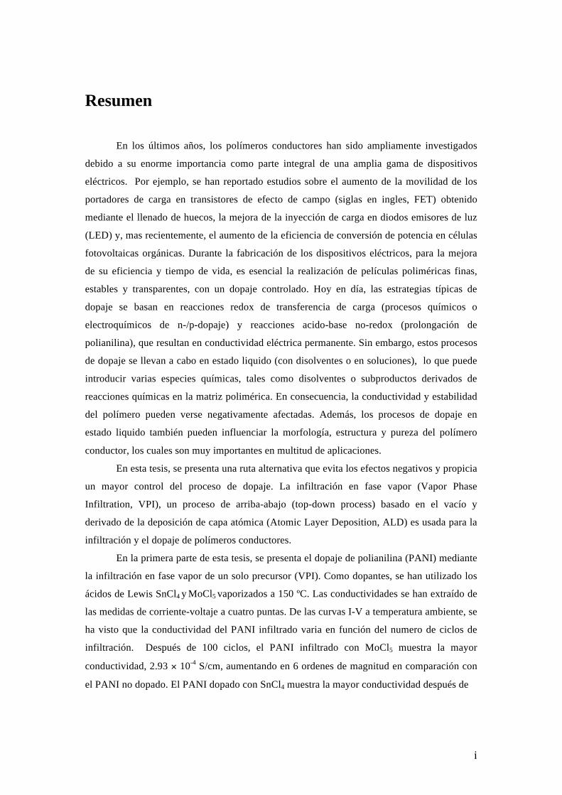
Curvas I-‐V de (a) PANI/1M HCl, PANI/MoCl5 (100 ciclos) and PANI/SnCl4 (60 ciclos) recién
preparados y (b) PANI/1M HCl, PANI/MoCl5 (100 ciclos) y PANI/SnCl4 (60 ciclos) después de
ser almacenados en vacío a 150 °C durante 100 minutos. El recuadro muestra el área a baja
corriente de la Figura 1b. Las conductividades de (c) MoCl5 y (d) SnCl4 en función de el
numero de ciclos de infiltración (medidos a temperatura ambiente). (e) Comparación de
conductividades de PANI/1M HCl, PANI/SnCl4 (60 ciclos) y PANI/MoCl5 (100 ciclos) recién
preparado, y después de ser almacenados en vacío a 150 °C durante 100 minutos.
Resumen
iii
60 ciclos de infiltración, con un valor de 1.03 × 10⁻⁵ S/cm, lo que supone un aumento de 5
ordenes de magnitud. Después de calentar las muestras dopadas a 150 ºC durante 100 minutos
en vacío, se observo que la conductividad del PANI dopado mediante el método tradicional
(1M HCl) se redujo en alrededor de 7 ordenes de magnitud, lo que podría deberse a la
deprotonación del PANI dopado y la evaporación del HCl.
La conductividad del PANI infiltrado con cloruros metálicos disminuyo mucho
menos, lo que indica que los cloruros metálicos están atrapados en la matriz polimérica dando
así mayor estabilidad al polímero dopado en condiciones severas. Las imágenes de SEM
muestran que el proceso VPI no altera la morfología del PANI, por lo que este proceso de
arriba-abajo puede usarse para el dopaje de PANI después de obtener la morfología deseada.
De acuerdo con los resultados obtenidos mediante FTIR, Raman y espectroscopia UV-vis, los
procesos de dopaje con MoCl5 y SnCl4 resultan en la oxidación del PANI y el presunto
complejamiento de los cloruros metálicos con los átomos de nitrógeno del PANI. En
consecuencia, la movilidad electrónica en las cadenas poliméricas aumenta
considerablemente y la estructura es estable incluso a temperaturas elevadas en vacío.
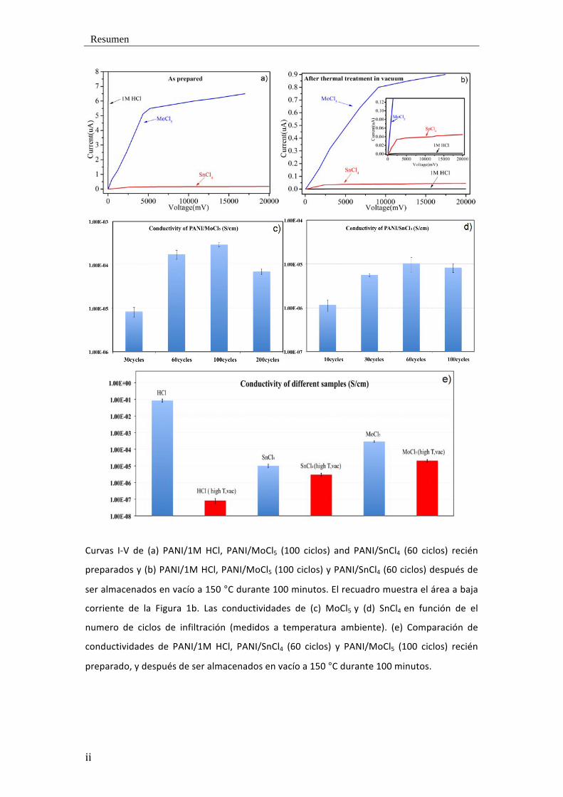
(a) Curvas I-‐V de P3HT sin dopar (negro) y P3HT dopado con MoCl5 después de 50
ciclos (rojo), 100 ciclos (azul) y 300 ciclos (cian); (b) comparación de conductividades de
P3HT sin dopar y P3HT dopado con MoCl5 después de varios ciclos de infiltración (30, 50,
100, 200 y 300 ciclos) a 70 °C.
Resumen
iv
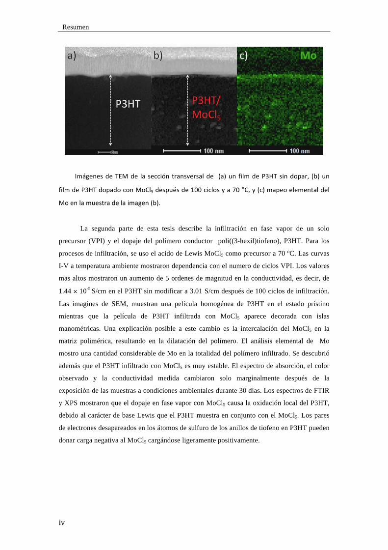
Imágenes de TEM de la sección transversal de (a) un film de P3HT sin dopar, (b) un
film de P3HT dopado con MoCl5 después de 100 ciclos y a 70 °C, y (c) mapeo elemental del
Mo en la muestra de la imagen (b).
La segunda parte de esta tesis describe la infiltración en fase vapor de un solo
precursor (VPI) y el dopaje del polímero conductor poli((3-hexil)tiofeno), P3HT. Para los
procesos de infiltración, se uso el acido de Lewis MoCl5 como precursor a 70 ºC. Las curvas
I-V a temperatura ambiente mostraron dependencia con el numero de ciclos VPI. Los valores
mas altos mostraron un aumento de 5 ordenes de magnitud en la conductividad, es decir, de
1.44 × 10⁻⁵ S/cm en el P3HT sin modificar a 3.01 S/cm después de 100 ciclos de infiltración.
Las imagines de SEM, muestran una película homogénea de P3HT en el estado prístino
mientras que la película de P3HT infiltrada con MoCl5 aparece decorada con islas
manométricas. Una explicación posible a este cambio es la intercalación del MoCl5 en la
matriz polimérica, resultando en la dilatación del polímero. El análisis elemental de Mo
mostro una cantidad considerable de Mo en la totalidad del polímero infiltrado. Se descubrió
además que el P3HT infiltrado con MoCl5 es muy estable. El espectro de absorción, el color
observado y la conductividad medida cambiaron solo marginalmente después de la
exposición de las muestras a condiciones ambientales durante 30 días. Los espectros de FTIR
y XPS mostraron que el dopaje en fase vapor con MoCl5 causa la oxidación local del P3HT,
debido al carácter de base Lewis que el P3HT muestra en conjunto con el MoCl5. Los pares
de electrones desapareados en los átomos de sulfuro de los anillos de tiofeno en P3HT pueden
donar carga negativa al MoCl5 cargándose ligeramente positivamente.
Resumen
v
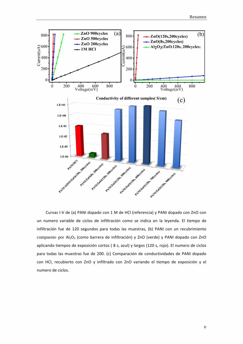
Curvas I-‐V de (a) PANI dopado con 1 M de HCl (referencia) y PANI dopado con ZnO con
un numero variable de ciclos de infiltración como se indica en la leyenda. El tiempo de
infiltración fue de 120 segundos para todas las muestras, (b) PANI con un recubrimiento
compuesto por Al2O3 (como barrera de infiltración) y ZnO (verde) y PANI dopado con ZnO
aplicando tiempos de exposición cortos ( 8 s, azul) y largos (120 s, rojo). El numero de ciclos
para todas las muestras fue de 200. (c) Comparación de conductividades de PANI dopado
con HCl, recubierto con ZnO y infiltrado con ZnO variando el tiempo de exposición y el
numero de ciclos.
Resumen
vi
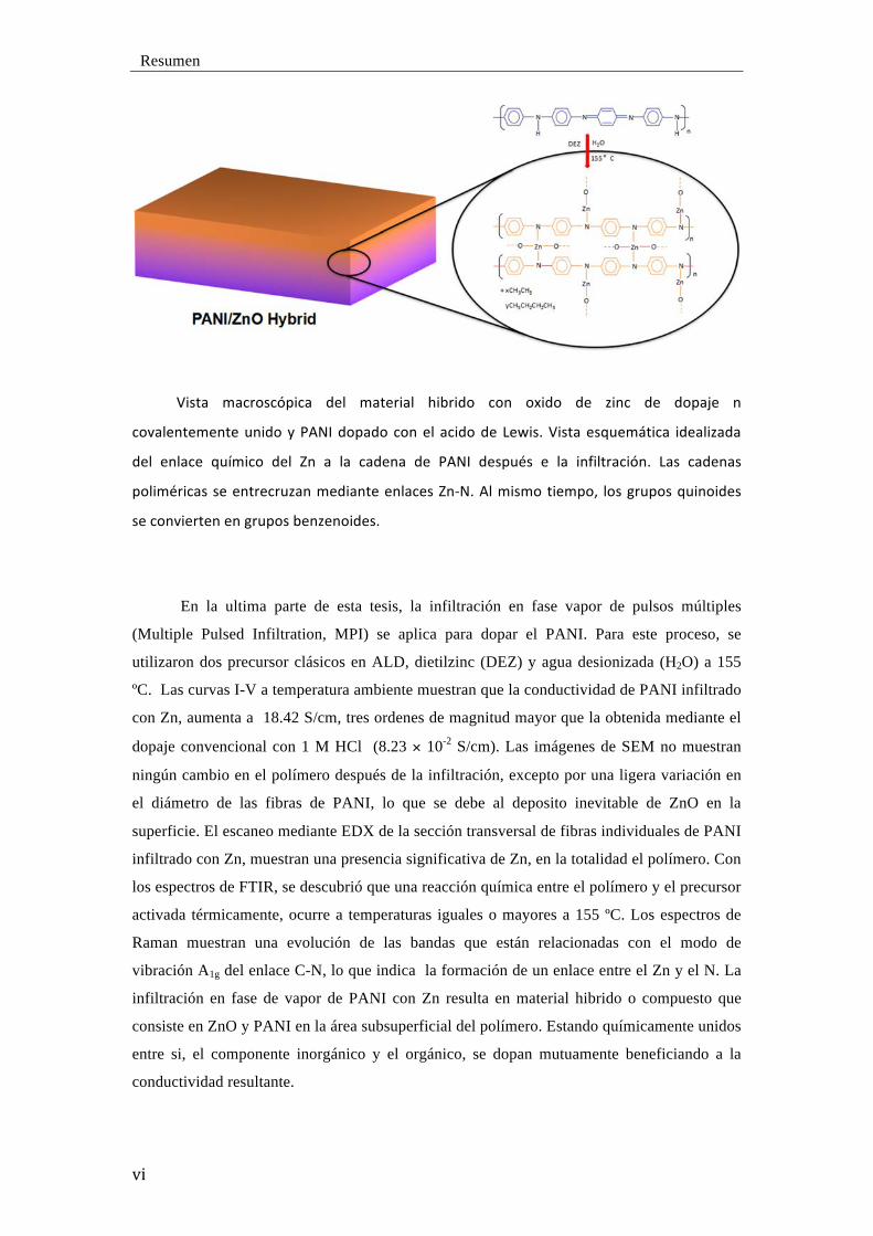
Vista macroscópica del material hibrido con oxido de zinc de dopaje n
covalentemente unido y PANI dopado con el acido de Lewis. Vista esquemática idealizada
del enlace químico del Zn a la cadena de PANI después e la infiltración. Las cadenas
poliméricas se entrecruzan mediante enlaces Zn-‐N. Al mismo tiempo, los grupos quinoides
se convierten en grupos benzenoides.
En la ultima parte de esta tesis, la infiltración en fase vapor de pulsos múltiples
(Multiple Pulsed Infiltration, MPI) se aplica para dopar el PANI. Para este proceso, se
utilizaron dos precursor clásicos en ALD, dietilzinc (DEZ) y agua desionizada (H2O) a 155
ºC. Las curvas I-V a temperatura ambiente muestran que la conductividad de PANI infiltrado
con Zn, aumenta a 18.42 S/cm, tres ordenes de magnitud mayor que la obtenida mediante el
dopaje convencional con 1 M HCl (8.23 × 10⁻² S/cm). Las imágenes de SEM no muestran
ningún cambio en el polímero después de la infiltración, excepto por una ligera variación en
el diámetro de las fibras de PANI, lo que se debe al deposito inevitable de ZnO en la
superficie. El escaneo mediante EDX de la sección transversal de fibras individuales de PANI
infiltrado con Zn, muestran una presencia significativa de Zn, en la totalidad el polímero. Con
los espectros de FTIR, se descubrió que una reacción química entre el polímero y el precursor
activada térmicamente, ocurre a temperaturas iguales o mayores a 155 ºC. Los espectros de
Raman muestran una evolución de las bandas que están relacionadas con el modo de
vibración A1g del enlace C-N, lo que indica la formación de un enlace entre el Zn y el N. La
infiltración en fase de vapor de PANI con Zn resulta en material hibrido o compuesto que
consiste en ZnO y PANI en la área subsuperficial del polímero. Estando químicamente unidos
entre si, el componente inorgánico y el orgánico, se dopan mutuamente beneficiando a la
conductividad resultante.
vii
Abstract Over the past years, conductive polymers have been extensively investigated due to
their tremendous importance as integral part of a wide range of electrical devices. For
instance, studies have reported on enhanced mobilites of charge carriers in field-effect
transistors (FETs) achieved by trap filling, improved charge injection in light-emitting diodes
(LEDs) and, more recently, superior power conversion efficiencies in organic-photovoltaics.
During the fabrication of the electrical devices, for improving their efficiency and lifetime, a
crucial step is the realization of stable and controllably doped transparent highly conducting
polymer thin films. Nowadays, the typical doping strategies for conducting polymers usually
rely on charge-transfer redox chemisty (chemical or electrochemical n-/p-doping processes),
and non-redox acid-base chemistry (protonation of polyaniline), which result in permanent
electrical conductivity. However, these doping processes are usually performed in the liquid
state (solvents or solutions), which can introduce various chemical species, such as solvents
or byproducts of chemical reactions, into the conducting polymer matrix, and in this way
bring about negative consequences for the conductivity and stability of the polymer. In
addition, doping processes in liquid state can also influence the morphology, structure and
purity of the conducting polymer, which are very important for various applications. In this
thesis, an alternative approach is introduced, which can avoid such negative influences and
provide better control of the doping process. The ¨ Vapor Phase infiltration ¨ (VPI), a vacuum
based process derived from the atomic layer deposition (ALD), is used for the top-down
infiltration and doping of conducting polymers.
In the first part of this thesis, a single precursor vapor phase infiltration (VPI) process
to dope polyaniline (PANI) is presented. As dopants, the vaporized Lewis acidic precursors
SnCl4 and MoCl5 were used at a process temperature of 150 °C. The conductivities are
extracted from four-point current-voltage measurements. From the room-temperature I-V
plots, it was found that the conductivities of the infiltrated PANI are a function of the
infiltration cycle number. After 100 cycles, the MoCl5-infiltrated PANI showed the highest
conductivity, 2.93 × 10⁻⁴ S/cm, which is a significant enhancement of up to 6 orders of
magnitude in comparison to undoped PANI. SnCl4-infiltrated PANI showed highest
conductivity after 60 cycles with a value of 1.03 × 10⁻⁵ S/cm. The enhancement amounted to
5 orders of magnitude. After heating the infiltrated samples at 150 °C in a vacuum
environment for 100 min, it was found that the conductivity of traditionally doped PANI (1M
HCl) decreased by nearly 7 orders of magnitude, which is likely to be due to the
deprotonation of the doped PANI and evaporation of HCl. The conductivities of the VPI
Abstract
viii
doped PANI decreased to a much lower extent, which indicates that the infiltrated metal
chlorides were trapped inside the polymer matrix, resulting in a higher stability of the doped
polymer even in a harsh environment. SEM images showed that the VPI process did not alter
the PANI morphology, thus the process can indeed be used for top-down doping after a
desired morphology of PANI has been obtained. According to the FTIR, Raman and UV-vis
spectra, the doping process with MoCl5 and SnCl4 results in an oxidation of PANI and
presumably in complexation of the metal chlorides with the nitrogen atoms of PANI. As a
result, the electron mobility along the polymer chains is significantly enhanced and the
structure is stabilized even at an elevated temperature in a vacuum environment.
The second part of this thesis describes the single precursor VPI and doping of poly(3-
hexyl)thiophene (P3HT). For the infiltration processes, the Lewis acid MoCl5 was used as
precursor at a process temperature of 70 °C. The room-temperature I-V plots show a
dependency on the VPI cycles numbers. The highest values show an increase of 5 orders of
magnitude for the conductivity, namely from 1.44 × 10⁻⁵ S/cm in the as-prepared P3HT to
3.01 S/cm after 100 infiltration cycles. SEM images show a homogeneous film of P3HT in
the pristine state, while the MoCl5-infiltrated P3HT thin film became decorated with
nanoscale islands. A possible reason for this change is the intercalation of MoCl5 into the
polymer martrix, resulting in a swelling of the polymer. Elemental mapping of Mo showed a
considerable amount of the metal inside the bulk of the infiltrated polymer. It was further
found that the MoCl5-infiltrated P3HT is temporally very stable. The absorption spectra, the
perceived color, and the measured conductivities only marginally changed upon exposure of
the samples to air in ambient conditions for 30 days. The FTIR and XPS spectra show that the
doping with MoCl5 from the vapor phase results in a local oxidation of P3HT, owing to the
Lewis basic character that P3HT shows in conjuction with MoCl5. The lone electron pairs at
the sulfur atoms of the thiophene rings in P3HT can donate negative charge to the MoCl5 with
themselves becoming rather positively charged.
In the last part of this thesis, the multiple pulsed vapor phase infiltration (MPI)
process was applied to dope polyaniline (PANI). For the process, the two typical ALD
precursors diethylzinc (DEZ) and deionized water (H2O) were used at a process temperature
of 155 °C. The room-temperature I-V polts showed the conductivity of Zn-infiltrated PANI
increasing to 18.42 S/cm, up to three orders of magnitude higher than obtained upon
conventional doping with 1 M HCl in wet-chemical ways (8.23 × 10⁻² S/cm). SEM images did
not show any obvious change of the polymer after infiltration, except a slight variation in the
PANI fiber diameters, which is due to the unavoidable surface-deposited ZnO. The TEM and
EDS scans of cross-sectioned regions of individual Zn-infiltrated PANI fibers show a
significant presence of Zn in the bulk of the polymer. From FTIR spectra, it was found that a
Abstract
ix
thermally actived chemical reaction between the polymer and precursor takes place, which at
temperatures equal or above 155 °C becomes pronounced. Raman spectra additionally
showed an evolution of bands, which are associated with the C-N vibrational A1g mode,
indicating the formation of a bond between Zn and N. Infiltration of PANI with Zn from the
vapor phase results in a hybrid or composite material consisting of ZnO and PANI in the
subsurface area of the polymer. Being chemically bound to each other, the inorganic and
organic components mutually dope each other for the benefit of the resulting conductivity.

Abstract
x
xi
Contents
Resumen .................................................................................................................................................... i
Abstract ................................................................................................................................................. vii
Contents .................................................................................................................................................. xi Chapter 1 Introduction ........................................................................................................................ 1
1.1Background ................................................................................................................................................. 1 1.2 Atomic Layer Deposition (ALD) .................................................................................................... 13 1.3 Vapor Phase Infiltration Process (VPI) ......................................................................................... 16 1.4 Objective and Structure of the Thesis ............................................................................................ 27
Chapter 2 Experimental Techniques and Methods .................................................................. 29 2.1 X-ray Diffractometer ........................................................................................................................... 29 2.2 Fourier Transform Infrared (FTIR) Spectroscopy ..................................................................... 31 2.3 Raman Spectroscopy ........................................................................................................................... 32 2.4 Electron Microscopy (SEM and TEM) ......................................................................................... 32 2.5 Ultraviolet -Visible Spectroscopy ................................................................................................... 34 2.6 Atomic Force Microscopy (AFM) .................................................................................................. 35 2.7 X-ray Photoelectron Spectroscopy (XPS) .................................................................................... 35 2.8 Assessment of the Electrical Conductivity .................................................................................. 36
Chapter 3 Tuning the Conductivity of Polyaniline (PANI) by VPI Process ................... 41 3.1. Introduction ........................................................................................................................................... 43 3.2. Experimental Section ......................................................................................................................... 44
3.2.1 Preparation the Polyaniline (PANI) nanofibers Thin Film ............................................ 44 3.2.2 Vapor Phase Infiltration Process of PANI Thin Film ..................................................... 44 3.2.3 Characterization ........................................................................................................................... 45
3.3 Results and Discussion ....................................................................................................................... 46 3.3.1 Assessment of the electrical conductivity ........................................................................... 46 3.3.2 FTIR Spectroscopy ..................................................................................................................... 48 3.3.3 Raman Spectroscopy .................................................................................................................. 50 3.3.4 SEM and EDX .............................................................................................................................. 52 3.3.5 Potential Reaction Schemes ..................................................................................................... 53
3.4 Conclusion .............................................................................................................................................. 55 Chapter 4 Controlling the Conductivity of Poly(3-hexyl)thiophe-ne (P3HT) by Low Temperature VPI Process ................................................................................................................. 57
4.1 Introduction ............................................................................................................................................ 59 4.2 Experimental Section .......................................................................................................................... 62 4.3 Results and Discussion ....................................................................................................................... 64
4.3.1 Assessment of the electrical conductivity ........................................................................... 64 4.3.2 UV-Vis spectroscopy ................................................................................................................. 65 4.3.3 Raman spectroscopy ................................................................................................................... 66 4.3.4 Infrared spectra ............................................................................................................................. 68 4.3.5 X-ray diffraction .......................................................................................................................... 69 4.3.6 SEM, AFM and TEM ................................................................................................................. 70
4.4 Conclusions ............................................................................................................................................ 72 Chapter 5 Conductive Polymer-Inorganic Hybrid Materials through Synergistic Mutual Doping of the Constituents ............................................................................................... 75
5.1 Introduction ............................................................................................................................................ 77

Contents
xii
5.2 Experimental Section .......................................................................................................................... 79 5.3 Results and Discussion ....................................................................................................................... 81
5.3.1 Assessment of the electrical conductivity ........................................................................... 81 5.3.2 Electron Microscopy .................................................................................................................. 84 5.3.3 Infrared Spectra ............................................................................................................................ 87 5.3.4 Raman Spectra .............................................................................................................................. 88 5.3.5 X-ray diffraction .......................................................................................................................... 89 5.3.6 X-ray Photoelectron Spectra .................................................................................................... 90
5.4 Conclusion .............................................................................................................................................. 93 Chapter 6 ................................................................................................................................................ 95 Bibliography ......................................................................................................................................... 97 List of Publications .......................................................................................................................... 111 Acknowledgements ......................................................................................................................... 113
1
Chapter 1
Introduction
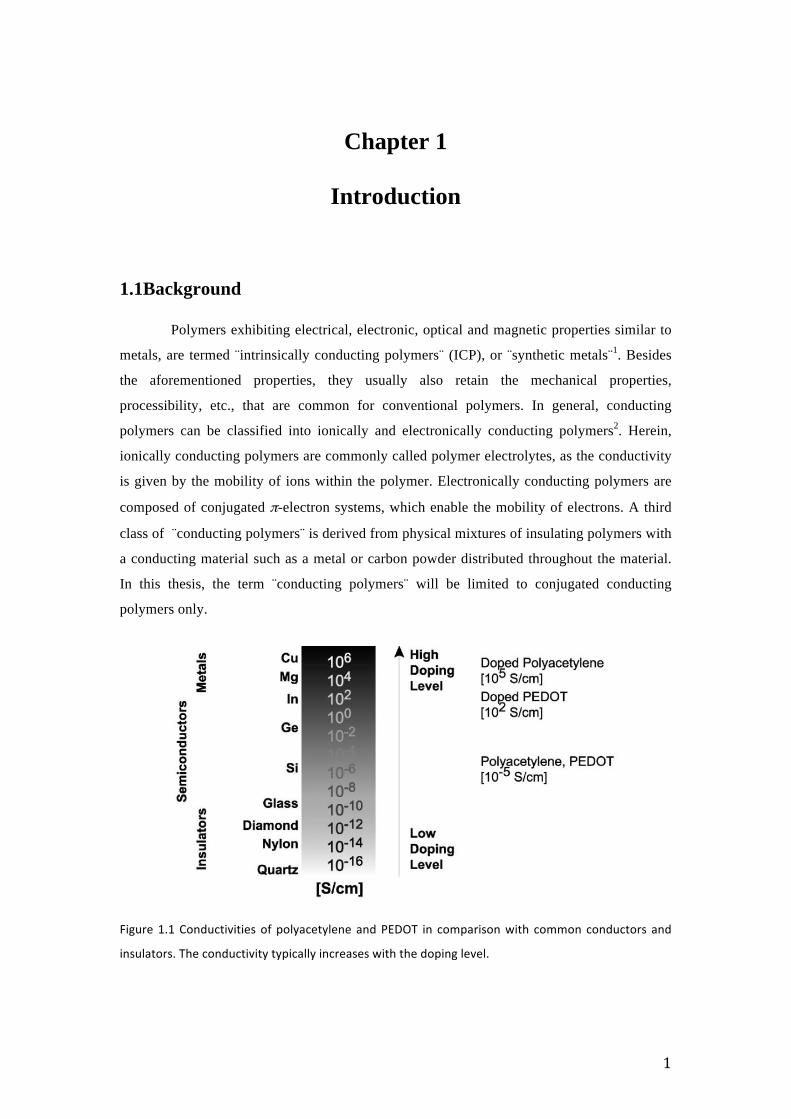
1.1Background Polymers exhibiting electrical, electronic, optical and magnetic properties similar to
metals, are termed ¨intrinsically conducting polymers¨ (ICP), or ¨synthetic metals¨1. Besides
the aforementioned properties, they usually also retain the mechanical properties,
processibility, etc., that are common for conventional polymers. In general, conducting
polymers can be classified into ionically and electronically conducting polymers2. Herein,
ionically conducting polymers are commonly called polymer electrolytes, as the conductivity
is given by the mobility of ions within the polymer. Electronically conducting polymers are
composed of conjugated π-electron systems, which enable the mobility of electrons. A third
class of ¨conducting polymers¨ is derived from physical mixtures of insulating polymers with
a conducting material such as a metal or carbon powder distributed throughout the material.
In this thesis, the term ¨conducting polymers¨ will be limited to conjugated conducting
polymers only.
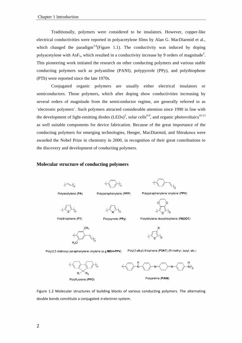
Figure 1.1 Conductivities of polyacetylene and PEDOT in comparison with common conductors and
insulators. The conductivity typically increases with the doping level.
Chapter 1 Introduction
)!
Traditionally, polymers were considered to be insulators. However, copper-like
electrical conductivities were reported in polyacetylene films by Alan G. MacDiarmid et al.,
which changed the paradigm3,4(Figure 1.1). The conductivity was induced by doping
polyacetylene with AsF5, which resulted in a conductivity increase by 9 orders of magnitude3.
This pioneering work initiated the research on other conducting polymers and various stable
conducting polymers such as polyaniline (PANI), polypyrrole (PPy), and polythiophene
(PTh) were reported since the late 1970s.
Conjugated organic polymers are usually either electrical insulators or
semiconductors. Those polymers, which after doping show conductivities increasing by
several orders of magnitude from the semiconductor regime, are generally referred to as
¨electronic polymers¨. Such polymers attracted considerable attention since 1990 in line with
the development of light-emitting diodes (LEDs)5, solar cells6-9, and organic photovoltaics10-13
as well suitable components for device fabrication. Because of the great importance of the
conducting polymers for emerging technologies, Heeger, MacDiarmid, and Shirakawa were
awarded the Nobel Prize in chemistry in 2000, in recognition of their great contributions to
the discovery and development of conducting polymers.
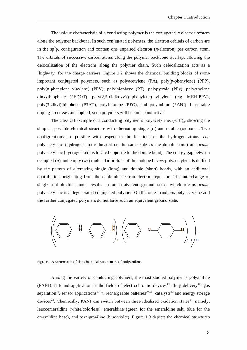
Molecular structure of conducting polymers
L<M"#,' 3HU' 486,;"6%#' &G#";G"#,&' 8O' D"<6+<=M' D68;_&' 8O' $%#<8"&' ;8=+";G<=M' B86CE,#&H' R[,' %6G,#=%G<=M'
+8"D6,'D8=+&';8=&G<G"G,'%';8=K"M%G,+'!!,6,;G#8='&C&G,EH''
Chapter 1 Introduction
'!
The unique characteristic of a conducting polymer is the conjugated !-electron system
along the polymer backbone. In such conjugated polymers, the electron orbitals of carbon are
in the sp2pz configuration and contain one unpaired electron (!-electron) per carbon atom.
The orbitals of successive carbon atoms along the polymer backbone overlap, allowing the
delocalization of the electrons along the polymer chain. Such delocalization acts as a
¨highway¨ for the charge carriers. Figure 1.2 shows the chemical building blocks of some
important conjugated polymers, such as polyacetylene (PA), poly(p-phenylene) (PPP),
poly(p-phenylene vinylene) (PPV), polythiophene (PT), polypyrrole (PPy), polyethylene
dioxythiophene (PEDOT), poly(2,5-dialkoxy)(p-phenylene) vinylene (e.g. MEH-PPV),
poly(3-alkyl)thiophene (P3AT), polyfluorene (PFO), and polyaniline (PANI). If suitable
doping processes are applied, such polymers will become conductive.
The classical example of a conducting polymer is polyacetylene, (-CH)n, showing the
simplest possible chemical structure with alternating single (") and double (!) bonds. Two
configurations are possible with respect to the locations of the hydrogen atoms: cis-
polyacetylene (hydrogen atoms located on the same side as the double bond) and trans-
polyacetylene (hydrogen atoms located opposite to the double bond). The energy gap between
occupied (!) and empty (!#) molecular orbitals of the undoped trans-polyacetylene is defined
by the pattern of alternating single (long) and double (short) bonds, with an additional
contribution originating from the coulomb electron-electron repulsion. The interchange of
single and double bonds results in an equivalent ground state, which means trans-
polyacetylene is a degenerated conjugated polymer. On the other hand, cis-polyacetylene and
the further conjugated polymers do not have such an equivalent ground state.
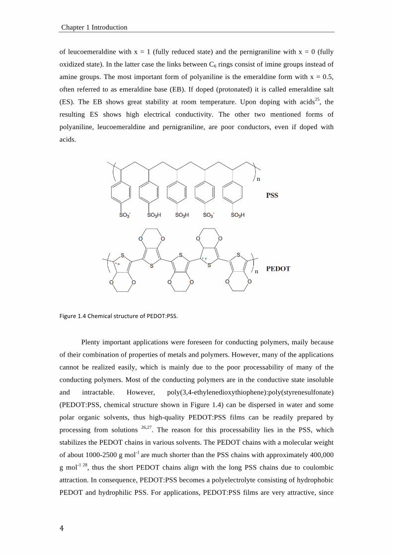
L<M"#,'3HQ'>;[,E%G<;'8O'G[,';[,E<;%6'&G#";G"#,&'8O'B86C%=<6<=,H'
Among the variety of conducting polymers, the most studied polymer is polyaniline
(PANI). It found application in the fields of electrochromic devices14, drug delivery15, gas
separation16, sensor applications17-19, rechargeable batteries20,21, catalysts22 and energy storage
devices23. Chemically, PANI can switch between three idealized oxidation states24, namely,
leucoemeraldine (white/colorless), emeraldine (green for the emeraldine salt, blue for the
emeraldine base), and pernigraniline (blue/violet). Figure 1.3 depicts the chemical structures
Chapter 1 Introduction
,!
of leucoemeraldine with x = 1 (fully reduced state) and the pernigraniline with x = 0 (fully
oxidized state). In the latter case the links between C6 rings consist of imine groups instead of
amine groups. The most important form of polyaniline is the emeraldine form with x = 0.5,
often referred to as emeraldine base (EB). If doped (protonated) it is called emeraldine salt
(ES). The EB shows great stability at room temperature. Upon doping with acids25, the
resulting ES shows high electrical conductivity. The other two mentioned forms of
polyaniline, leucoemeraldine and pernigraniline, are poor conductors, even if doped with
acids.
L<M"#,'3H?'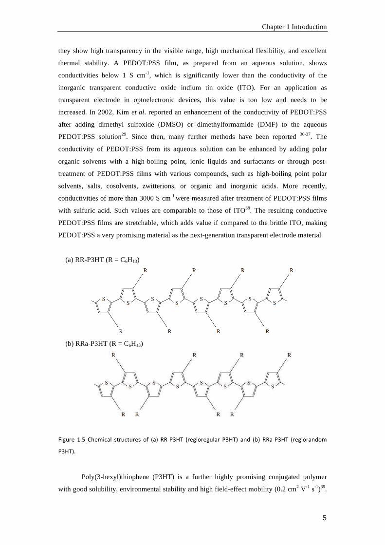
Chapter 1 Introduction
-!
they show high transparency in the visible range, high mechanical flexibility, and excellent
thermal stability. A PEDOT:PSS film, as prepared from an aqueous solution, shows
conductivities below 1 S cm-1, which is significantly lower than the conductivity of the
inorganic transparent conductive oxide indium tin oxide (ITO). For an application as
transparent electrode in optoelectronic devices, this value is too low and needs to be
increased. In 2002, Kim et al. reported an enhancement of the conductivity of PEDOT:PSS
after adding dimethyl sulfoxide (DMSO) or dimethylformamide (DMF) to the aqueous
PEDOT:PSS solution29. Since then, many further methods have been reported 30-37. The
conductivity of PEDOT:PSS from its aqueous solution can be enhanced by adding polar
organic solvents with a high-boiling point, ionic liquids and surfactants or through post-
treatment of PEDOT:PSS films with various compounds, such as high-boiling point polar
solvents, salts, cosolvents, zwitterions, or organic and inorganic acids. More recently,
conductivities of more than 3000 S cm-1 were measured after treatment of PEDOT:PSS films
with sulfuric acid. Such values are comparable to those of ITO38. The resulting conductive
PEDOT:PSS films are stretchable, which adds value if compared to the brittle ITO, making
PEDOT:PSS a very promising material as the next-generation transparent electrode material.
(a) RR-P3HT (R = C6H13)
(b) RRa-P3HT (R = C6H13)
L<M"#,' 3H9' 
Chapter 1 Introduction
6
The transport mechanism of the charge carriers in P3HT has attracted great attention from the
viewpoint of physics. P3HT has a non-degenerate electronic structure and polarons or
bipolarons are considered to be the dominant charge carriers40. The most important
characteristic of P3HT is its regioregularity, i.e., the percentage of stereoregular head-to-tail
attachments of the hexyl side-chains to the thiophene rings. At room temperature, the
difference in the charge-carrier mobilities of the regioregular and regionrandom isomers, the
structure of which are shown in Figure 1.5 (a) and (b), may be at least two orders of
magnitude. In regioregular P3HT (RR-P3HT), the hexyl side chains on adjacent thiophene
rings are ordered in an alternating head-to-tail conformation, while in regiorandom P3HT
(RRa-P3HT), the hexyl side chains are arranged randomly with 50% being a head-to-tail
conformation. In the case of RR-P3HT, owing to the self-packing of the hexyl side chains
driven by hydrophobic interactions, the self-stacking of thiophene rings between adjacent
polymer chains facilitates the formation of ordered microcrystalline regions with a lamellar
structure that improves the carrier mobility41,42.
Charge carriers in the conducting polymers For π-conjugated conducting polymers, solitons, polarons and bipolarons are proposed
to interpret the enhancement of conductivity after doping. In the case of the conjugated trans-
polyacetylene with a degenerate basic state, the charge carriers are solitons and polarons,
while in the nondegenerate cis-polyacetylene, polyaniline, polypyrrole, and polythiophene,
etc., in their basic state polarons and bipolarons act as charge carriers. The soliton is formed
by an unpaired π-electron resulting from the formation of radicals44. It can be delocalized
along the conjugated trans-polyacetylene chain45,46. The neutral soliton can be either oxidized
to lose an electron and form a positive soliton, or reduced to gain an electron and form a
negative soliton. Due to the unpaired electron, the soliton possesses a spin of 1/2, whereas the
positive and negative solitons have no spin. The electronic energy level of the soliton is
located in the middle of the bandgap of trans-polyacetylene.
Polarons are the main charge-carriers in conducting polymers, such as the degenerate
basic state trans-polyacetylene and other non-degenerate basic state conjugated polymers.
The positive polaron is a radical cation with positive charge, and the negative polaron is a
radical anion with negative charge. The positive polaron is formed after oxidation of the
conjugated polymer chain, and the negative polaron is formed after its reduction. The
appearance of the polarons produces two new polaron energy levels in the bandgap of the
conjugated polymers. Both the positive polaron and negative polaron possess a spin of 1/2.
Bipolarons are charge carriers with double charges, resulting from coupling of two positive or
Chapter 1 Introduction
7
negative polarons within a conjugated polymer chain. The bipolaron has no spin. Generally,
positive and negative bipolarons correspond to the model of holes and electron pairs.
Doping Chracteristics The charge injection into conjugated, semiconducting macromolecular chains, termed
¨doping¨, is typically dissimilar to the doping process of the traditional inorganic
semiconductors silicon and germanium. The polymer doping process results in various
interesting and important phenomena that define this research field47. Controlled introduction
of impurities into the semicondutor matrix is the common method to dope inorganic
semiconductors. Such procedure allows for deliberately tuning the band alignment at
interfaces and markedly increasing the conductivity already at ultralow doping ratios. The
reason is that each covalently bound dopant atom donates one mobile charge to the highly
crystalline and ultra-pure semiconductor matrix48,49. In contrast, the doping process of
conjugated polymers involves either charge-transfer redox chemistry, that is, the chemical
reduction (n-type doping) or oxidation (p-type doping) donates or retrieves electrons to or
from the π electron system of the polymer backbone50,51, or acid-base chemistry, which is
usually applied upon doping of polyaniline47. In the n-doped state, the main chain of the
polymer is reduced and a cation is electrostatically bound for keeping the overall charge of
the whole molecule neutral. Excess electrons within the main chain make the polymer n-type
conductive. In the p-doped state, the polymer is oxidized and the opposite case occurrs. The
resulting empty electron orbitals correspond to holes in semiconductors and make the
polymer a p-type conductor. Upon doping, an initially insulating or semiconducting polymer
with conductivities in the range of 10-10 to 10-5 S/cm becomes metallically conducting with
conductivities between 1 and 104 S/cm1. A controlled addition of small non-stoichiometric
quantities of dopants usually results in significant changes in the electronic, electrical,
magnetic, optical, and structural properties of the conjugated polymer. Importantly, the
doping process is reversible. Appropriate chemical treatment will restore the original
conjugated polymer with little or no effect on the polymer structure. Both, the doping and the
dedoping process, may be carried out chemically or electrochemically. Besides, also some
doping processes that do not introduce dopant ions are known52. Such processes
include ¨photo-doping¨ and ¨charge-injection doping¨. In those processes, transitory ¨doped¨
species are produced, which have similar spectroscopic signatures to polymers that contain
dopant ions.
Chapter 1 Introduction
8
(1) Chemical doping
Polyacetylene can be made conductive by chemical doping. Depending on the selected
chemical process the polymer may become either p-or n-type conducting.
p-doping, also called partial oxidation doping, is achieved with a partial oxidation
process of the conjugated π-electron system of the polymer backbone in order to create
polarons. Among the possible p-dopants, I2, Br2, AsF5, or (NO)PF6 are the most common
ones. After a p-doping process with I2, the conductivity of trans-polyacetylene or trans-(CH)x
typically increases from ca. 10-5 S/cm to ca. 103 S/cm3,4. The following reaction illustrates the
underlying chemical pocess53,54.
trans-(CH)x + 1.5 xyI2 è [CH+y(I3)y-]x (y≤0.07)
In contrast, n-doping is a partial reduction process of the π-electron system of a
conjugated polymer in order to create negative charge carriers. Some strong reducing agents,
such as alkali metals, alkaline earth metals, liquid sodium amalgam or sodium naphthaline
(Na(Nphth))3, etc., can be used as n-type dopants. After treating trans-(CH)x with Na(Nphth),
its antibonding π-electron system is partially populated with electrons, resulting in the
conductivity of the polymer increasing up to 103 S/cm. The following reaction illustrates the
underlying chemical process 53,54.
trans-(CH)x + xyNa+(Nphth)- è [Nay+(CH)-y]x + Nphth (y≤0.1)
(2) Electrochemical doping
Although chemical doping is an efficient process, it is often difficult to control.
Quantitative doping to the highest charge carrier concentrations results in reasonably high
quality materials. However, attempting to obtain intermediate doping levels often makes the
doping inhomogeneous. Therefore, electrochemical doping was introduced to solve this
problem55. Such doping is performed by electrochemical oxidation or reduction of a
conjugated polymer placed onto an electrode. During the electrochemical doping process, the
electrode supplies charge to the conjugated polymer and a redox reaction is induced, while
ions from the electrolyte diffuse into the polymer to compensate the overall electronic charge.
The doping level is determined by the potential applied between the conjugated polymer and
the counter electrode; in equilibrium, the doping level is precisely defined by that voltage.
Thus, doping at any level can be obtained by setting the electrochemical cell to a defined
Chapter 1 Introduction
9
potential and allowing the system to reach an electrochemical equilibrium, where no current
flows.
Electrochemical p-doping can be accomplished by anodic oxidation. The conjugated
polymer chain becomes oxidized and loses an electron, while gaining a hole. The charges are
balanced with counteranions (ClO4-) from the electrolyte solution. The following reaction
illustrates the process on the example of trans-(CH)x being immersed into a solution of
LiClO4 in propylene carbonate55.
trans-(CH)x + (xy) ( ClO4)- è [(CH)+y( ClO4)-y]x + (xy)e- (y≤0.1)
Likewise, electrochemical n-doping can be carried out by cathodic reduction. The
conjugated polymer main chain becomes reduced and gains an electron. The charges are
balanced with countercations (Li+) from the electrolyte solution. The following reaction
illustrates the process on the example of trans-(CH)x being immersed into a solution of
LiClO4 dissolved in tetrahydrofuran56.
trans-(CH)x + (xy) Li+ + (xy)e- è [Liy+(CH)-y]x (y≤0.1)
Chapter 1 Introduction
&/!
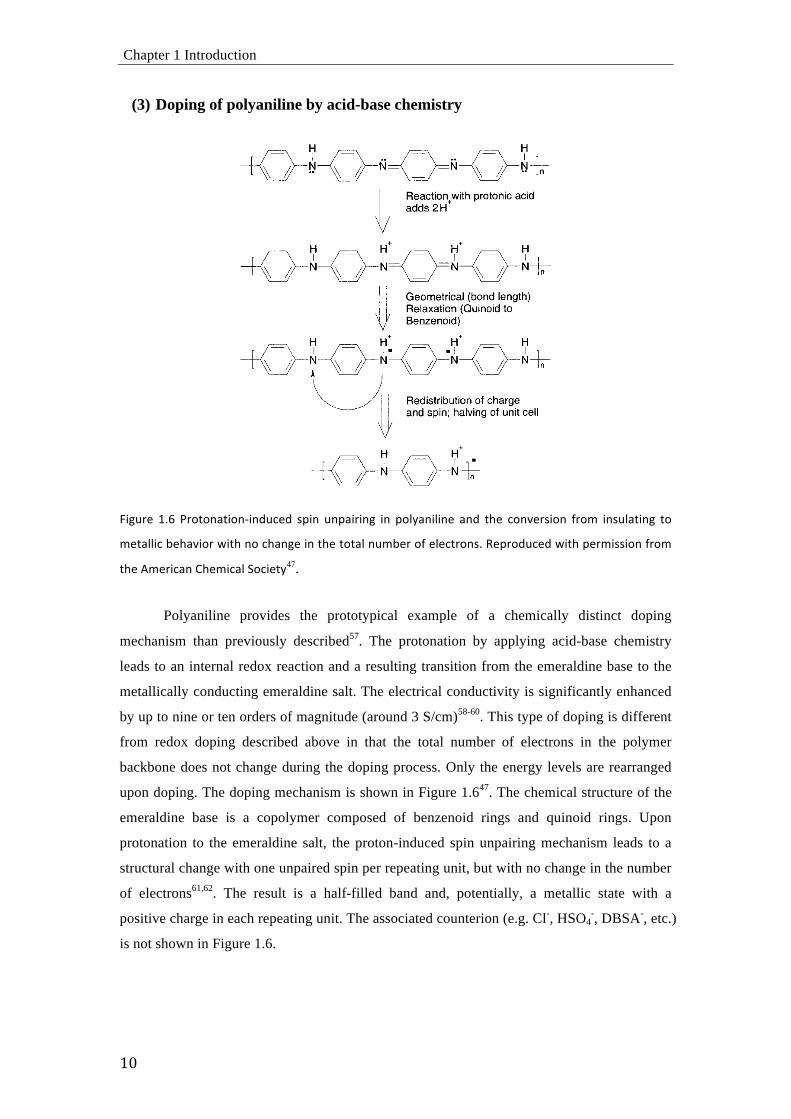
(3) Doping of polyaniline by acid-base chemistry
L<M"#,' 3H@' /#8G8=%G<8=)<=+";,+' &B<=' "=B%<#<=M' <=' B86C%=<6<=,' %=+' G[,' ;8=$,#&<8=' O#8E' <=&"6%G<=M' G8'
E,G%66<;'D,[%$<8#'\<G['=8';[%=M,'<='G[,'G8G%6'="ED,#'8O',6,;G#8=&H'a,B#8+";,+'\<G['B,#E<&&<8='O#8E'
G[,'0E,#<;%='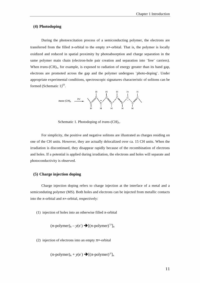
Chapter 1 Introduction
&&!
(4) Photodoping
During the photoexcitation process of a semiconducting polymer, the electrons are
transferred from the filled $-orbital to the empty $#-orbital. That is, the polymer is locally
oxidized and reduced in spatial proximity by photoabsorption and charge separation in the
same polymer main chain (electron-hole pair creation and separation into ¨free¨ carriers).
When trans-(CH)x, for example, is exposed to radiation of energy greater than its band gap,
electrons are promoted across the gap and the polymer undergoes ¨photo-doping¨. Under
appropriate experimental conditions, spectroscopic signatures characteristic of solitons can be
formed (Schematic 1)63.
Schematic 1. Photodoping of trans-(CH)x.
For simplicity, the positive and negative solitons are illustrated as charges residing on
one of the CH units. However, they are actually delocalized over ca. 15 CH units. When the
irradiation is discontinued, they disappear rapidly because of the recombination of electrons
and holes. If a potential is applied during irradiation, the electrons and holes will separate and
photoconductivity is observed.
(5) Charge injection doping
Charge injection doping refers to charge injection at the interface of a metal and a
semiconduting polymer (MS). Both holes and electrons can be injected from metallic contacts
into the $-orbital and $#-orbital, respectively:
(1) injection of holes into an otherwise filled $-orbital
($-polymer)n – y(e-) ![($-polymer)+y]n
(2) injection of electrons into an empty $#-orbital
($-polymer)n + y(e-) ![($-polymer)-y]n
Chapter 1 Introduction
12
In the case of charge injection at an MS interface, the conjugated polymer becomes
reduced or oxidized, that is, electrons are added to the empty π∗-orbital or removed from the
filled π-orbital. However, the polymer is not doped in the chemical or electrochemical sense,
because no counterions are introduced during the charge injection doping process. With
charge injection doping, even superconductivity was observed in a polythiophene derivate.
The application of an appropriate potential across the MS interface can lead to a surface
charge layer, the ¨accumulation¨ layer, that has been extensively investigated for conducting
polymers52,64,65. In some conjugated polymer, such as P3HT or polyacetylene (CH)x, the
resulting charges evolve without the presence of a dopant ion. Spectroscopic studies of (CH)x
show signatures characteristic of solitons and a mid-gap absorption band observed in
chemically and electrochemically doped polymers.
Each of the mentioned charge-injection doping methods can result in unique and
important phenomena. Electrical conductivity induced by chemical and/or electrochemical
doping methods is permanent, but only as long as the carriers are chemically compensated or
until the carriers are removed on purpose by a ¨dedoping¨ process. Upon photoexcitation, the
photoconductivity is transient, and lasts only until the excited species are either trapped or
decay back to the ground state. In the case of charge injection at the metal-semiconductor
(MS) interface, only a biasing voltage is applied, the electrons can enter the π∗-orbital and/or
the holes enter the π-orbital.
In consequence, for obtaining permanent electrical conductivity, the best doping
strategies are the chemical and/or electrochemical processes. However, such doping processes
are usually performed in liquid state, which can introduce various chemical species, solvents
or byproducts into the polymer matrix. This may have various negative consequences for the
conductivity or stability of the polymer. The morphology, structure and purity, which are
very important for many applications, such as, field-effect transistors (FETs)66-68, light
emitting diodes (LEDs)69-71, and organic photovoltaics72-74, etc. will be influenced. For
avoiding these negative influences and avoiding liquid state doping processes, a vacuum
based process, the Vapor Phase Infiltration75, which is derived from atomic layer deposition
(ALD)76,77, can be exploited for the top-down infiltration and doping of conducting polymers.
This new approach is described in this thesis.
Chapter 1 Introduction
13
1.2 Atomic Layer Deposition (ALD)
Atomic layer deposition: general concepts
Atomic layer deposition (ALD), originally called atomic layer epitaxy (ALE), was
developed in the 1970s by Suntola et al. to meet the needs of fabricating high-quality and
large-area ZnS films for a use in thin-film electro-luminescent flat panel displays78. The first
application of such a display was the display board at the Helsinki Airport installed in 1982.
Since then, more than 2 million electro-luminescent displays have been fabricated with this
new process79. Since it was found that most of the films grown in this way do not show
epitaxial type of growth, the new deposition method was renamed to Atomic Layer
Deposition (ALD). In the middle of 1990s, ALD was identified as method-of-choice for
manufacturing microelectronic devices80,81. Its enormous take off occurred in the 2000s,
motivated by the need of miniaturizing the dimensions of devices and increasing aspect ratios
in integrated circuits. Molecular layer deposition (MLD), an organic modification of ALD,
evolved after Yoshimura et al. deposited polyimide films applying the same operating
principle as in ALD, but with organic molecules. It was first referred to as either alternating
vapor deposition, vapor deposition polymerization, or layer-by-layer growth82-84. Recently,
molecular layer deposition (MLD), as well as combinations of it with ALD, have brought
about various hybrid organic/inorganic materials with new and/or altered properties in
comparison to the individual or parent materials.
Atomic layer deposition is a unique technique for the deposition of conformal, pinhole
free and homogeneous thin films. It can be considered as a similar, although chemically
distinct, case of the chemical vapor deposition (CVD). The difference among them refers to
the chemical reaction being separated into two self-limiting and individual surface reactions85.
The separation of the reactions is achieved by keeping the precursors separate during the
process. Such a separation brings about a self-limiting growth mechanism and thus leads to
the control of the film growth on the atomic/molecular level. While the CVD process deposits
materials as a function of time, ALD films grow as a function of the cycle number. Figure 1.7
schematically illustrates a growth cycle of a metal oxide (MO2) by ALD, in which M stands
for any metal, such as Ti, Zr, or Hf. For such deposition, a metal-containing precursor ML4 (L:
ligand) is used as metal source and H2O as oxygen source. One such MO2 ALD deposition
cycle consists of following steps: 1) pulse of the first precursor, ML4, 2) its chemisorption and
surface saturation during exposure, 3) purge to remove excess precursor, and 4) pulse of the
second precursor, H2O, followed by 5) its reaction with the adsorbed ML4 during exposure,
and 6) purge to remove excess H2O and reaction byproducts (Figure 1.7 (a)). In step 1, the
Chapter 1 Introduction
14
surface is exposed to the ML4 vapor pulse. The precursor can react with the functional surface
sites to form a stable and saturative chemisorbed layer. After purging the excess ML4 vapor
and byproducts, the same procedure is repeated with H2O vapor to complete a full ALD
growth cycle. These steps are repeated and each cycle will add a sub-monolayer quantity of
the deposit to the surface until a thin MO2 film is formed. The growth per cycle (GPC) is
defined as the average added to the growing film per full cycle. The self-limitation of the
surface reactions in ALD allows a thickness control simply by controlling the number of
cylces86.
In both, the ALD and CVD processes, all surfaces exposed to the precursor vapor are
being coated. This indicates that highly uniform thin films can be formed on various
substrates. However, in contrast to ALD, where the two precursors are temporally separated
(Figure 1.7 (b)), in CVD the vaporized precursors are simultaneously fed into the reactor with
a carrier gas (Figure 1.7 (c)). With this procedure, the precursor lifetime in a CVD process is
not long enough to diffuse into deep cavities of complicated 3D substrates prior to the
reaction with the counter precursor. Thus, the CVD process will produce less conformal thin-
films than the ALD process, especially with structurally complicated substrates.
Chapter 1 Introduction
&-!
(a)
(b) (c)
L<M"#,'3HV'>;[,E%G<;'8O'%='0N^24N^'B#8;,&&'\<G['%';8EB%#<&8='G8'%'!*^'B#8;,&&H'-%.'0N^'<&'%';C;6<;'
%=+' &,6O)6<E<G<=M' B#8;,&&7' \[,#,' %' &"D&G#%G,' <&' ,YB8&,+' G8' G[,' B#,;"#&8#' 4N?' -3.7' G[,' B#,;"#&8#'
&%G"#%G,&' %=+' <&' B"#M,+' -U7Q.7' G[,' &,;8=+' B#,;"#&8#' <&' B"6&,+7' <=' G[<&' ;%&,' 5UX' -?.7' %=+' O<=%66C' G[,
&,;8=+'B#,;"#&8#'%=+'DCB#8+";G&'B"#M,+'[email protected]'(='%'GCB<;%6'B#8;,&&7'G[,'&"#O%;,';[,E<&G#C'<&'#,&G8#,+'
%G'G[,',=+'8O',%;[';C;6,H'-D.'I'%=+'/'+,=8G,',YB8&"#,'%=+'B"#M,7'#,&B,;G<$,6CH'R[,'%6G,#=%G<=M'I'%=+'/'
&G,B&';#,%G,'%='%6G,#=%G<=M'B#,&&"#,'B#8O<6,'%&'%'O"=;G<8='8O'G<E,7'\[<6,'%'!*^'B#8;,&&'-;.'[%&'%'=,%#6C'
;8=&G%=G' B#,&&"#,' B#8O<6,7' \[,#,' G[,' B#,;"#&8#&' %#,' <=G#8+";,+' <=G8' G[,' #,%;G8#' &<E"6G%=,8"&6CH'
a,B#8+";,+'\<G['B,#E<&&<8=7'b<6,C)*!585.
Chapter 1 Introduction
&(!
L<M"#,' 3HZ' >;[,E%G<;' 8O' G[,' 0N^' B#8;,&&' \<=+8\H' (=O6",=;,' 8O' G[,' +,B8&<G<8=' G,EB,#%G"#,' 8=' G[,'
M#8\G['#%G,H
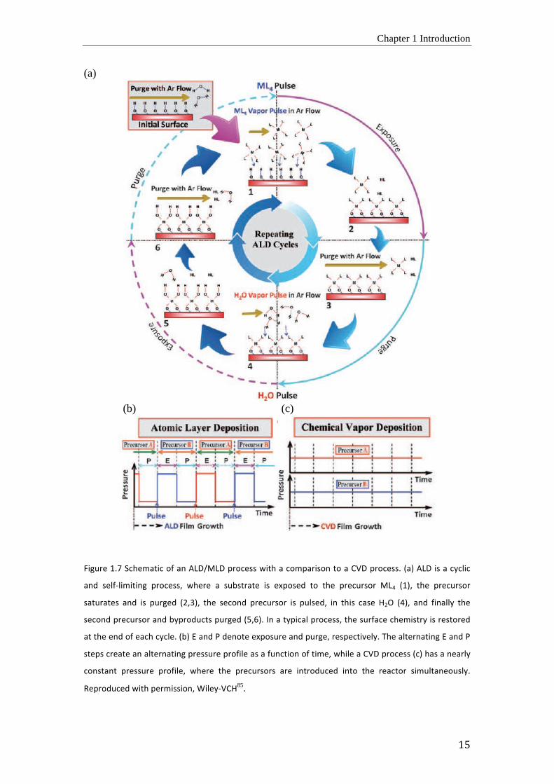
During the ALD process, a determining parameter for the growth rate is the deposition
temperature. Figure 1.8 shows the so-called idealized ¨ALD-window¨, which defines the
temperature range in which the thin film formation occurs under self-limiting conditions.
Outside this temperature range, the growth is limited by various factors. At lower
temperatures, the precursors may condense on the substrate, which can lead to CVD like
growth, or the surface reaction may not happen because of insufficient activation energy. At
too high temperatures, precursor decomposition may bring about an enhanced ALD growth
rate, or the thermal energy may be too high, resulting in desorption of the precursor from
substrate86-88.
1.3 Vapor Phase Infiltration (VPI)
1.3.1 Bio-inspired background of VPI
Most living organisms rely on hard tissues for support, protection, nutrition, and
defense. Biomineralization is the dominant strategy in nature for hardening of soft tissue and
manifests an astonishing diversity of bioceramic structures with exquisite microarchitectures
that show specific physical properties as a result of environmental adaptation89-91. Although
the variety of architectures appears virtually infinite, Ca-, Si-, and Fe-based minerals are the
Chapter 1 Introduction
17
most commonly encountered92. As a basic principle, the hardness of these composites is
largely governed by the type of mineral incorporated93 and the degree of mineralization94.
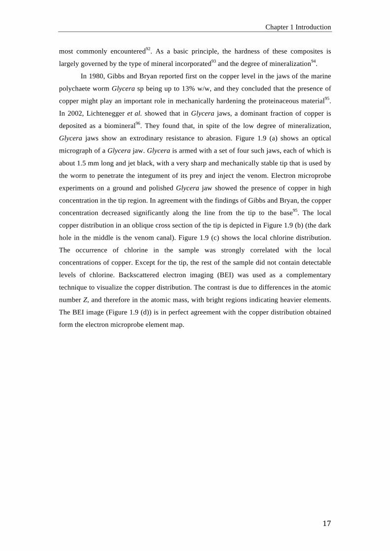
In 1980, Gibbs and Bryan reported first on the copper level in the jaws of the marine
polychaete worm Glycera sp being up to 13% w/w, and they concluded that the presence of
copper might play an important role in mechanically hardening the proteinaceous material95.
In 2002, Lichtenegger et al. showed that in Glycera jaws, a dominant fraction of copper is
deposited as a biomineral96. They found that, in spite of the low degree of mineralization,
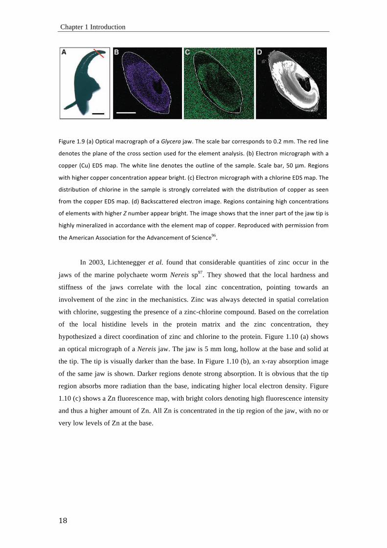
Glycera jaws show an extrodinary resistance to abrasion. Figure 1.9 (a) shows an optical
micrograph of a Glycera jaw. Glycera is armed with a set of four such jaws, each of which is
about 1.5 mm long and jet black, with a very sharp and mechanically stable tip that is used by
the worm to penetrate the integument of its prey and inject the venom. Electron microprobe
experiments on a ground and polished Glycera jaw showed the presence of copper in high
concentration in the tip region. In agreement with the findings of Gibbs and Bryan, the copper
concentration decreased significantly along the line from the tip to the base95. The local
copper distribution in an oblique cross section of the tip is depicted in Figure 1.9 (b) (the dark
hole in the middle is the venom canal). Figure 1.9 (c) shows the local chlorine distribution.
The occurrence of chlorine in the sample was strongly correlated with the local
concentrations of copper. Except for the tip, the rest of the sample did not contain detectable
levels of chlorine. Backscattered electron imaging (BEI) was used as a complementary
technique to visualize the copper distribution. The contrast is due to differences in the atomic
number Z, and therefore in the atomic mass, with bright regions indicating heavier elements.
The BEI image (Figure 1.9 (d)) is in perfect agreement with the copper distribution obtained
form the electron microprobe element map.
Chapter 1 Introduction
&.!
L<M"#,'3Hc'-%.'XBG<;%6'E%;#8M#%B['8O'%'"#$%&'('K%\H'R[,'&;%6,'D%#';8##,&B8=+&'G8':HU'EEH'R[,'#,+'6<=,'
+,=8G,&'G[,'B6%=,'8O'G[,';#8&&'&,;G<8='"&,+'O8#'G[,',6,E,=G'%=%6C&<&H'-D.'I6,;G#8='E<;#8M#%B['\<G['%
;8BB,#' -!".'I^>'E%BH'R[,'\[<G,' 6<=,'+,=8G,&' G[,'8"G6<=,'8O' G[,' &%EB6,H' >;%6,'D%#7'9:'µEH'a,M<8=&'
\<G['[<M[,#';8BB,#';8=;,=G#%G<8='%BB,%#'D#<M[GH'-;.'I6,;G#8='E<;#8M#%B['\<G['%';[68#<=,'I^>'E%BH'R[,'
+<&G#<D"G<8='8O' ;[68#<=,' <=' G[,' &%EB6,' <&' &G#8=M6C' ;8##,6%G,+'\<G[' G[,'+<&G#<D"G<8='8O' ;8BB,#' %&' &,,='
O#8E'G[,';8BB,#'I^>'E%BH'-+.'d%;_&;%GG,#,+',6,;G#8='<E%M,H'a,M<8=&';8=G%<=<=M'[<M[';8=;,=G#%G<8=&'
8O',6,E,=G&'\<G['[<M[,#')'="ED,#'%BB,%#'D#<M[GH'R[,'<E%M,'&[8\&'G[%G'G[,'<==,#'B%#G'8O'G[,'K%\'G<B'<&'
[<M[6C'E<=,#%6<S,+'<='%;;8#+%=;,'\<G['G[,',6,E,=G'E%B'8O';8BB,#H'a,B#8+";,+'\<G['B,#E<&&<8='O#8E'
G[,'0E,#<;%='0&&8;<%G<8='O8#'G[,'0+$%=;,E,=G'8O'>;<,=;,96.
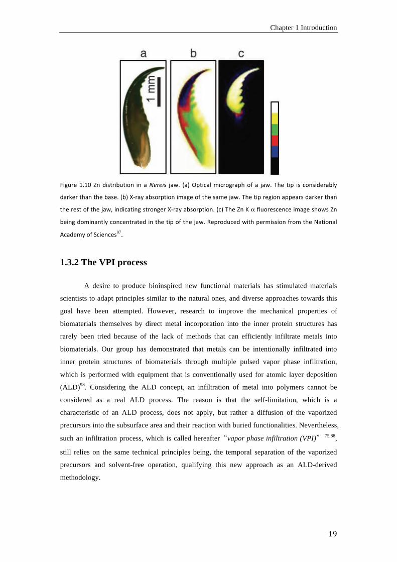
In 2003, Lichtenegger et al. found that considerable quantities of zinc occur in the
jaws of the marine polychaete worm Nereis sp97. They showed that the local hardness and
stiffness of the jaws correlate with the local zinc concentration, pointing towards an
involvement of the zinc in the mechanistics. Zinc was always detected in spatial correlation
with chlorine, suggesting the presence of a zinc-chlorine compound. Based on the correlation
of the local histidine levels in the protein matrix and the zinc concentration, they
hypothesized a direct coordination of zinc and chlorine to the protein. Figure 1.10 (a) shows
an optical micrograph of a Nereis jaw. The jaw is 5 mm long, hollow at the base and solid at
the tip. The tip is visually darker than the base. In Figure 1.10 (b), an x-ray absorption image
of the same jaw is shown. Darker regions denote strong absorption. It is obvious that the tip
region absorbs more radiation than the base, indicating higher local electron density. Figure
1.10 (c) shows a Zn fluorescence map, with bright colors denoting high fluorescence intensity
and thus a higher amount of Zn. All Zn is concentrated in the tip region of the jaw, with no or
very low levels of Zn at the base.
Chapter 1 Introduction
&+!
L<M"#,' 3H3:' W=' +<&G#<D"G<8=' <=' %'*&'&+,' K%\H' -%.'XBG<;%6'E<;#8M#%B['8O' %' K%\H' R[,' G<B' <&' ;8=&<+,#%D6C'
+%#_,#'G[%='G[,'D%&,H'-D.'e)#%C'%D&8#BG<8='<E%M,'8O'G[,'&%E,'K%\H'R[,'G<B'#,M<8='%BB,%#&'+%#_,#'G[%='
G[,'#,&G'8O'G[,'K%\7'<=+<;%G<=M'&G#8=M,#'e)#%C'%D&8#BG<8=H'-;.'R[,'W='f'%'O6"8#,&;,=;,'<E%M,'&[8\&'W='
D,<=M'+8E<=%=G6C';8=;,=G#%G,+'<='G[,'G<B'8O'G[,'K%\H a,B#8+";,+'\<G['B,#E<&&<8='O#8E'G[,'1%G<8=%6'
0;%+,EC'8O'>;<,=;,&97.
1.3.2 The VPI process
A desire to produce bioinspired new functional materials has stimulated materials
scientists to adapt principles similar to the natural ones, and diverse approaches towards this
goal have been attempted. However, research to improve the mechanical properties of
biomaterials themselves by direct metal incorporation into the inner protein structures has
rarely been tried because of the lack of methods that can efficiently infiltrate metals into
biomaterials. Our group has demonstrated that metals can be intentionally infiltrated into
inner protein structures of biomaterials through multiple pulsed vapor phase infiltration,
which is performed with equipment that is conventionally used for atomic layer deposition
(ALD)98. Considering the ALD concept, an infiltration of metal into polymers cannot be
considered as a real ALD process. The reason is that the self-limitation, which is a
characteristic of an ALD process, does not apply, but rather a diffusion of the vaporized
precursors into the subsurface area and their reaction with buried functionalities. Nevertheless,
such an infiltration process, which is called hereafter vapor phase infiltration (VPI) 75,88,
still relies on the same technical principles being, the temporal separation of the vaporized
precursors and solvent-free operation, qualifying this new approach as an ALD-derived
methodology.
Chapter 1 Introduction
)/!
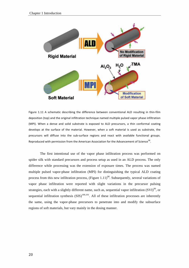
L<M"#,' 3H33' 0' &;[,E%G<;' +,&;#<D<=M' G[,' +<OO,#,=;,' D,G\,,=' ;8=$,=G<8=%6' 0N^' #,&"6G<=M' <=' G[<=)O<6E'
+,B8&<G<8='-G8B.'%=+'G[,'8#<M<=%6'<=O<6G#%G<8='G,;[=<]",'=%E,+'E"6G<B6,'B"6&,+'$%B8#'B[%&,'<=O<6G#%G<8='
-4/(.H' b[,=' %' +,=&,' %=+' &86<+' &"D&G#%G,' <&' ,YB8&,+' G8' 0N^' B#,;"#&8#&7' %' G[<=' ;8=O8#E%6' ;8%G<=M'
+,$,68B&' %G' G[,' &"#O%;,' 8O' G[,' E%G,#<%6H' 58\,$,#7' \[,=' %' &8OG' E%G,#<%6' <&' "&,+' %&' &"D&G#%G,7' G[,'
B#,;"#&8#&' \<66' +<OO"&,' <=G8' G[,' &"D)&"#O%;,' #,M<8=&' %=+' #,%;G' \<G[' %$%<6%D6,' O"=;G<8=%6' M#8"B&H'
a,B#8+";,+'\<G['B,#E<&&<8='O#8E'G[,'0E,#<;%='0&&8;<%G<8='O8#'G[,'0+$%=;,E,=G'8O'>;<,=;,98.
The first intentional use of the vapor phase infiltration process was performed on
spider silk with standard precursors and process setup as used in an ALD process. The only
difference while processing was the extension of exposure times. The process was named
multiple pulsed vapor-phase infiltration (MPI) for distinguishing the typical ALD coating
process from this new infiltration process, (Figure 1.11)98. Subsequently, several variations of
vapor phase infiltration were reported with slight variations in the precursor pulsing
strategies, each with a slightly different name, such as, sequential vapor infiltration (SVI)99, or
sequential infiltration synthesis (SIS)100,101. All of these infiltration processes are inherently
the same, using the vapor-phase precursors to penetrate into and modify the subsurface
regions of soft materials, but vary mainly in the dosing manner.
Chapter 1 Introduction
)&!
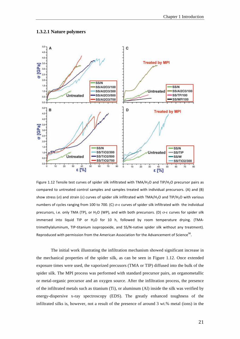
1.3.2.1 Nature polymers
L<M"#,'3H3U R,=&<6,'G,&G';"#$,&'8O'&B<+,#'&<6_'<=O<6G#%G,+'\<G['R4025UX'%=+'R(/25UX'B#,;"#&8# B%<#&'%&'
;8EB%#,+'G8'"=G#,%G,+';8=G#86'&%EB6,&'%=+'&%EB6,&' G#,%G,+'\<G['<=+<$<+"%6'B#,;"#&8#&H' -0.'%=+'-d.'
&[8\'&G#,&&'-".'%=+'&G#%<='-&.';"#$,&'8O'&B<+,#'&<6_'<=O<6G#%G,+'\<G['R4025UX'%=+'R(/25UX'\<G['$%#<8"&'
="ED,#&'8O';C;6,&'#%=M<=M'O#8E'3::'G8'V::H'-!.'")&';"#$,&'8O'&B<+,#'&<6_'<=O<6G#%G,+'\<G[''G[,'<=+<$<+"%6'
B#,;"#&8#&7' <H,H'8=6C'R40'-R/.7'8#'5UX'-b/.7'%=+'\<G['D8G['B#,;"#&8#&H' -^.'")&';"#$,&' O8#'&B<+,#'&<6_'
<EE,#&,+' <=G8' 6<]"<+' R(/' 8#' 5UX' O8#' 3:' [7' O8668\,+' DC' #88E' G,EB,#%G"#,' +#C<=MH' -R40)
G#<E,G[C6%6"E<="E7' R(/)G<G%=<"E' <&8B#8B8Y<+,7' %=+' >>21)=%G<$,' &B<+,#' &<6_' \<G[8"G' %=C' G#,%GE,=G.H'
a,B#8+";,+'\<G['B,#E<&&<8='O#8E'G[,'0E,#<;%='0&&8;<%G<8='O8#'G[,'0+$%=;,E,=G'8O'>;<,=;,98.
The initial work illustrating the infiltration mechanism showed significant increase in
the mechanical properties of the spider silk, as can be seen in Figure 1.12. Once extended
exposure times were used, the vaporized precusors (TMA or TIP) diffused into the bulk of the
spider silk. The MPI process was performed with standard precursor pairs, an organometallic
or metal-organic precursor and an oxygen source. After the infiltration process, the presence
of the infiltrated metals such as titanium (Ti), or aluminum (Al) inside the silk was verified by
energy-dispersive x-ray spectroscopy (EDS). The greatly enhanced toughness of the
infiltrated silks is, however, not a result of the presence of around 3 wt.% metal (ions) in the
Chapter 1 Introduction
))!
bulk of the protein, but of the chemical interaction between precursors and the substrate. The
X-ray diffraction (XRD) characterization and the analysis of the full width at the half
maximum (FWHM) of the peaks in the XRD spectra of the spider silk have shown that the
reactive metal-containing precursors can decrease the size of the beta-sheets in the protein
fibers during the infiltration process. The redistribution of the ratio of amorphous and
crystalline protein fractions and the size change of the beta-sheets finally changed the
mechanical properties significantly. Solid state nuclear magnetic resonance (NMR) spectra
indicated an interaction between aluminum and the protein backbone, crosslinking the
strands98. It was found that during the infiltration process, hydrogen bonds within the protein
were replaced with new covalent bonds between the metals and the protein matrix.
L<M"#,' 3H3Q' !8EB%#<&8=' 8O' #,B#,&,=G%G<$,' a%E%=' D%=+' &[<OG&' 8O' -%.' G[,' =%G<$,' ->>21.' %=+' -D.' 06)
<=O<6G#%G,+' ->>206.' &B<+,#' +#%M6<=,' &<6_' "B8=' E,;[%=<;%6' +,O8#E%G<8=H' -(=&,G&.' XBG<;%6' E<;#8&;8B,'
<E%M,&' &[8\<=M' G[,' O8;"&,+' 6%&,#'D,%E' -@QQ'=E.H'a,B#8+";,+'\<G['B,#E<&&<8=' O#8E'G[,'0E,#<;%='
Chapter 1 Introduction
23
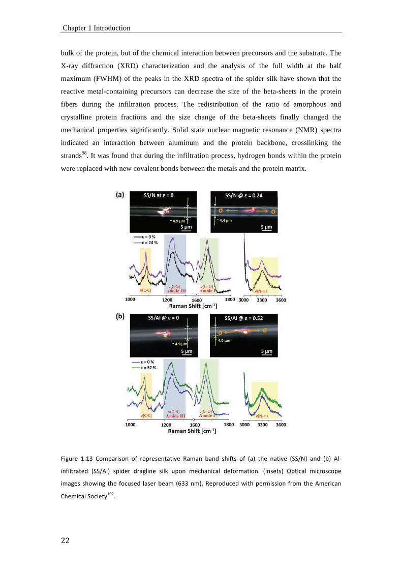
The influence of the organometallic precursor on the mechanical properties of the
spider silk was further investigated in a recent in situ Raman spectroscopic study of aluminum
infiltrated spider dragline silk102,103, as shown in Figure 1.13. Raman spectroscopy is a well-
established technique for evaluating molecular structures of materials and appears most useful
for examining molecular deformation mechanisms of the silks during mechanical
loading104,105. Upon mechanical deformation of the silk fiber, the covalent bonds within the
protein structures are stressed. This leads to an alignment of the molecules along the direction
of tension. The deformation of the oriented molecules in both the crystalline and amorphous
regions gives rise to a change in bond lengths and bond angles. This induces a change in the
corresponding force constants, which can be monitored by measuring the related Raman
shifts. Single fibers of both native and Al-infiltrated silks were deformed under controlled
strain. In parallel, changes in Raman bands related to amide I, amide III, ν(N-H) stretching
modes106, and ν(C-C) skeletal stretching modes were traced to identify the differences in the
molecular deformation behavior between the untreated and treated silk. Figure 1.13 shows the
Raman spectra of both silks upon uniaxial deformation in tension. While the native silk
showed Raman band shifts to lower wavenumbers (particularly, amide I, amide III, and ν(C-
C) stretching), the Al-infiltrated silk showed less significant shifts. However, the peaks of
amide III and ν(N-H) stretching modes of Al-infiltrated silk exhibited noticeable changes in
the peak shapes, which implies that the infiltrated Al atoms are affecting the hydrogen bonds.
Presumably the Al atoms form covalent bonds with amino acids during the infiltration of
highly reactive TMA and water precursors107,108.
Chapter 1 Introduction
),!
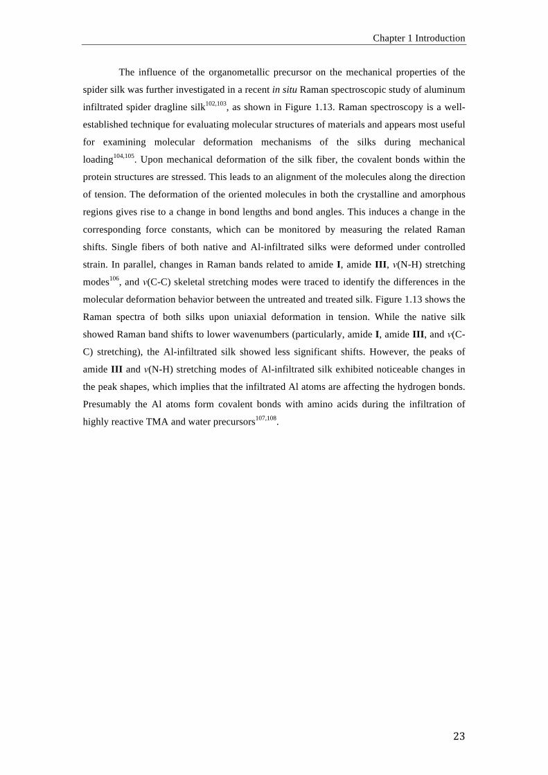
L<M"#,'3H3?'4,;[%=<;%6'B#8B,#G<,&'8O'<=O<6G#%G,+';,66"68&,'8DG%<=,+'O#8E'"=<%Y<%6'G,=&<6,'G,&G&H'-%.'R[,'
G,=&<6,' &G#,=MG[ &[8\&' %' U)Q O86+ <=;#,%&,' O8#' ;,66"68&,' <=O<6G#%G,+'\<G['^IW -+<,G[C6S<=;. %BB6C<=M ?'
<=O<6G#%G<8=' ;C;6,&7' \[<6,' ;,66"68&,' <=O<6G#%G,+' \<G[' R40' -G#<E,G[C6%6"E<="E.' &[8\&' 8=6C' %' &6<M[G'
<=;#,%&,H'-D.'R[,',6%&G<;'E8+"6"&'8O';,66"68&,'<=O<6G#%G,+'\<G['^IW'%BB6C<=M'?';C;6,&'&[8\&'%'''UH9)O86+
<=;#,%&,7'\[<6,';,66"68&,'<=O<6G#%G,+'\<G['R40'&[8\&'8=6C'%'&E%66';[%=M,H'a,B#8+";,+'\<G['B,#E<&&<8='
O#8E'G[,'0E,#<;%='
Chapter 1 Introduction
)-!
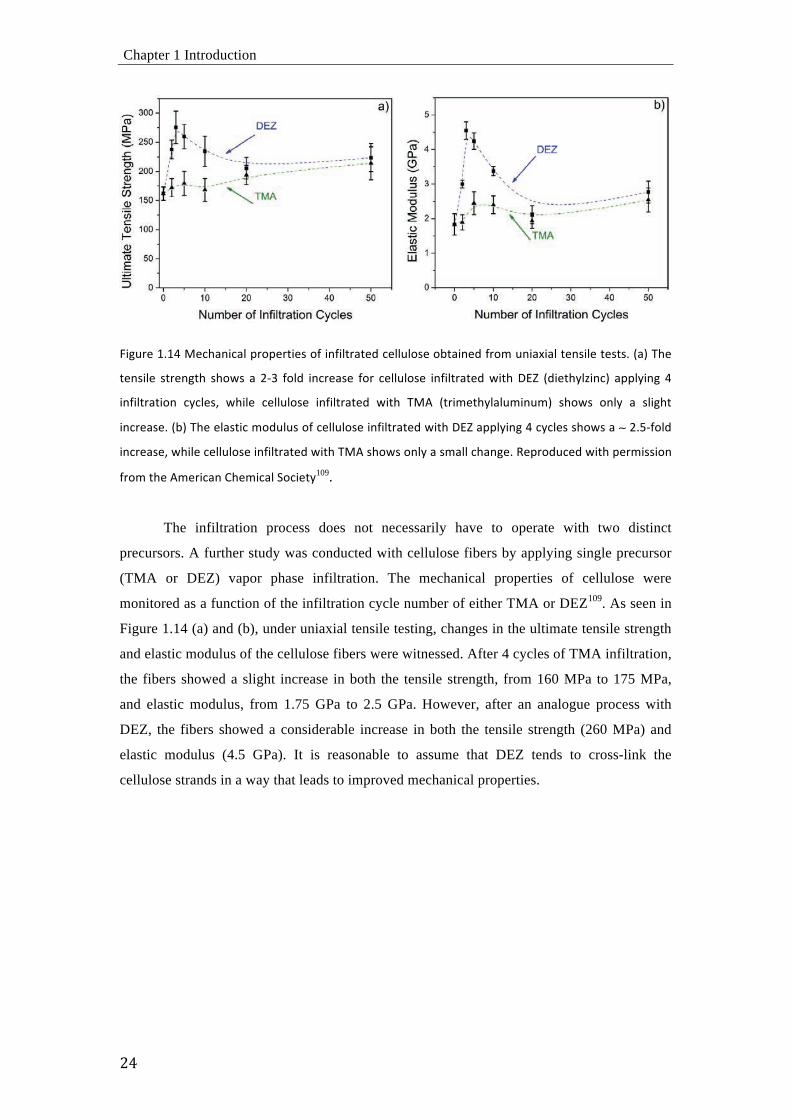
1.3.2.2 Synthetic polymers
L<M"#,' 3H39'g=<%Y<%6' G,=&<6,' D,[%$<8#' -,=M<=,,#<=M' &G#,&&7'"7' %=+' &G#%<=7'#.' 8O' =%G<$,' -/RLI21.7' [,%G)
G#,%G,+' -/RLI25.7'%=+'W=X' <=O<6G#%G,+'/RLI' -/RLI2?::';C;6,&'%=+'/RLI29::';C;6,&.H'R[,' <=&,G'B<;G"#,'
&[8\&'%'/RLI' &%EB6,'"&,+' O8#' G[,'"=<%Y<%6' G,=&<6,' G,&GH' -/RLI)B86CG,G#%O6"8#8,G[C6,=,.H'a,B#8+";,+'
\<G['B,#E<&&<8='O#8E'b<6,C)*!5110.
It has been already recognized for a while that incorporation of transition metals into
synthetic polymers can lead to unique physical/chemical properties and application in many
areas, including mechanics, optics, electronics, etc111-115. In order to show the applicability of
the vapor phase infiltration also to synthetic polymers, Lee et al. exposed PTFE
(polytetrafluoroethylene) to the precursor pair DEZ/H2O at a temperature of 70 °C110. It was
found that VPI can lead to an incorporation of Zn even into PTFE and chemically react with
the polymer even at such mild conditions. Under uniaxial tensile testing, the maximum stress
("max) of PTFE has increased from 11.50 MPa (PTFE/H) to 16.64 MPa (PTFE/400) and 23.14
MPa (PTFE/500) (Figure 1.15). A comparison of experimental and theoretically modeled
Raman spectra showed that the formation of -Zn-O-Zn- bridging units or –Zn-F groups at
both defect sites and polymer chain terminal is likely the reason for the modified mechanical
properties.
Chapter 1 Introduction
)(!
L<M"#,'3H3@H'>;[,E%G<;'8O'%='06UXQ'<=O<6G#%G<8='B#8;,&&'\<G['%'B86CE,#'\<G[8"G'O"=;G<8=%6'M#8"B&H'R[,'
B#,;"#&8#&'-R40'%=+'5UX.';%='D,'%D&8#D,+'DC'G[,'B86CE,#'%=+'#,%;G'<='G[,'&"D&"#O%;,'%#,%H'R[,'RI4'
<E%M,' &[8\&' %' M#%+,+'B86CE,#2<=8#M%=<;' <=G,#O%;,' %=+' %' #8"M[' &"#O%;,' G,YG"#,' <=' %' B86CB#8BC6,=,'
O<D,#'%OG,#';8%G<=M'"&<=M'R4025UXH'a,B#8+";,+'\<G['B,#E<&&<8='O#8E'I6&,$<,#116.
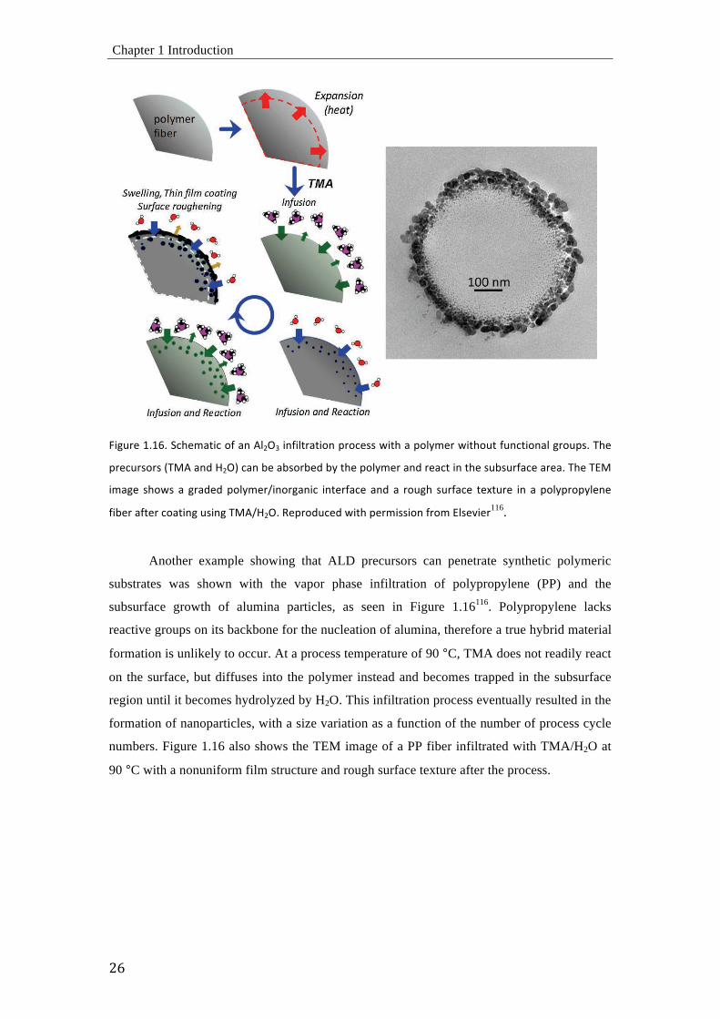
Another example showing that ALD precursors can penetrate synthetic polymeric
substrates was shown with the vapor phase infiltration of polypropylene (PP) and the
subsurface growth of alumina particles, as seen in Figure 1.16116. Polypropylene lacks
reactive groups on its backbone for the nucleation of alumina, therefore a true hybrid material
formation is unlikely to occur. At a process temperature of 90 °C, TMA does not readily react
on the surface, but diffuses into the polymer instead and becomes trapped in the subsurface
region until it becomes hydrolyzed by H2O. This infiltration process eventually resulted in the
formation of nanoparticles, with a size variation as a function of the number of process cycle
numbers. Figure 1.16 also shows the TEM image of a PP fiber infiltrated with TMA/H2O at
90 °C with a nonuniform film structure and rough surface texture after the process.
Chapter 1 Introduction
)*!
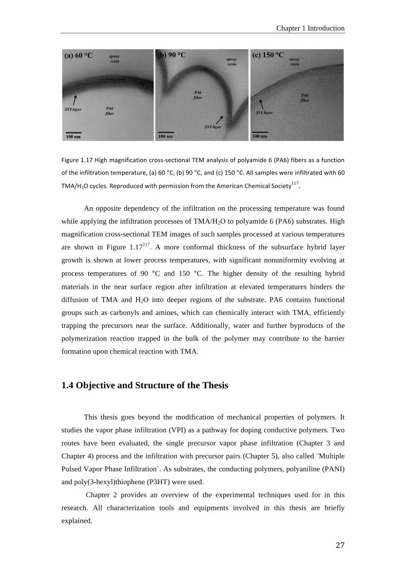
L<M"#,'3H3V'5<M['E%M=<O<;%G<8=';#8&&)&,;G<8=%6'RI4'%=%6C&<&'8O'B86C%E<+,'@'-/0@.'O<D,#&'%&'%'O"=;G<8='
8O'G[,'<=O<6G#%G<8='G,EB,#%G"#,7'-%.'@:'°!7'-D.'c:'°!7'%=+'-;.'39:'°!H'066'&%EB6,&'\,#,'<=O<6G#%G,+'\<G['@:'
R4025UX';C;6,&H'a,B#8+";,+'\<G['B,#E<&&<8='O#8E'G[,'0E,#<;%='
Chapter 1 Introduction
28
Chapter 3 focuses on the single precursor vapor phase infiltration and doping of the
emeraldine base of polyaniline (PANI) with SnCl4 and MoCl5. The conductivities of the
infiltrated PANI upon application of various cycle numbers and the stability of the infiltrated
polymer upon exposure to high temperatures (150 °C) and vacuum environment were studied,
and a likely doping mechanism was proposed.
Chapter 4 describes the low temperature single precursor MoCl5 vapor phase
infiltration and doping of poly(3-hexyl)thiophene (95% regioregularity), P3HT. The
conductivities of the infiltrated P3HT after various cycle numbers and its long-term stability
under ambient conditions were investigated. An appropriate doping mechanism is proposed
based on the performed characterization.
Chaper 5 describes the infiltration and doping of PANI (emeraldine base) with the
precursor pair DEZ (diethylzinc) and H2O, referred to as mulitiple pulsed vapor phase
infiltration of PANI. The conductivities of the infiltrated PANI after various infiltration cycle
numbers were explored. A doping mechanism is proposed, which is likely to result in a
mutually enhancing electronic interaction between two doped species, the ZnO and PANI.
Finally, a summary of the research and future perspectives are given in Chapter 6.
29
Chapter 2
Experimental Techniques and Methods
This chapter gives an overview of the experimental techniques and methods used in
the thesis. All the characterization tools mainly relate to structural, compositional, or
electronic characterizations. Specific methods applied in individual parts of the work will be
described in the relevant sections.
2.1 X-ray Diffractometer
X-ray diffractometry (XRD) is a technique, which allows to characterize the
crystallinity of a sample. In the reflectivity mode it can be used for measuring the thickness of
a thin film. In XRD, a monochromatic X-ray beam irradiates the sample at a grazing incident
angle θ. In a crystalline arrangement of atoms, the incident beam will be scattered with the
deflected waves having constructive interference at specific spots. In agreement with the
Braggʹ′s equation118,
2dsinθ = nλ,
diffraction will occur. At an angle 2θ with respect to the incident beam, a detector collects the
deflected beam. Figure 2.1 (a) shows schematically the beam path upon interaction with the
sample. Here, d is the spacing between diffracting planes, θ is the incident angle of the beam,
and λ is the wavelength of the beam. The detected reflections are subsequently indexed to
obtain the crystalline information in the reciprocal space. The X-ray reflectivity (XRR) technique is used to measure the thicknesses of a thin
film, based on the principle shown in Figure 2.1 (b). According to the Snell Law, the
refractive index of all materials is below the unity for X-ray electromagnetic radiation.
Therefore, the critical incident angle θc for total reflection will depend on the density of the
material. If the incident angle θ is equal to θc, the incident X-ray will propagate along the
sample surface. If the incident angle is below θc, total refelction will occur. With incident
angles above θc, the X-ray will be partly refracted and a reflection will occur at both the thin
film bottom and top interfaces. These two reflected waves will interfere with each other,
leading to the intensity decreasing as a function of the incident angle. From Snell’s Law:
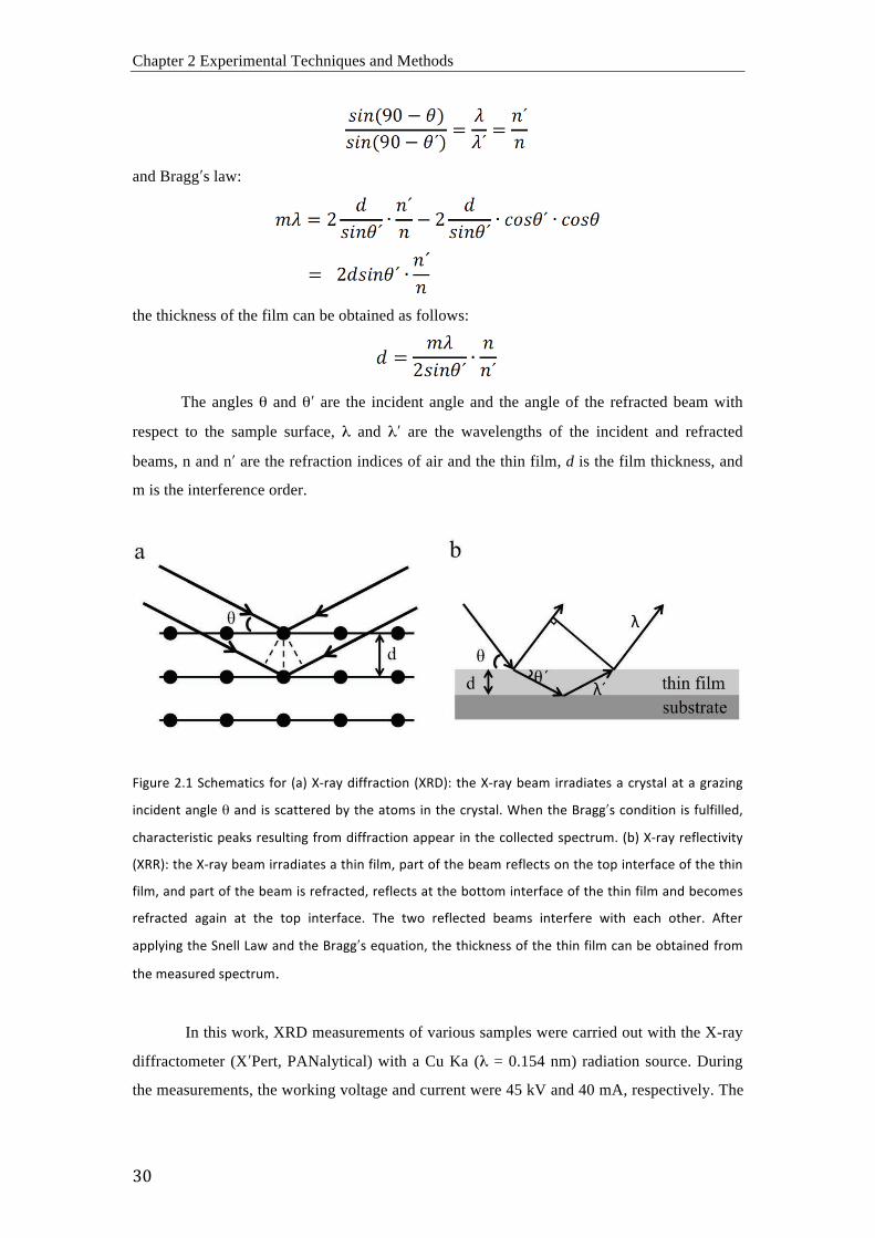
Chapter 2 Experimental Techniques and Methods
'/!
and Bragg)s law:
the thickness of the film can be obtained as follows:
The angles ( and () are the incident angle and the angle of the refracted beam with
respect to the sample surface, * and *) are the wavelengths of the incident and refracted
beams, n and n) are the refraction indices of air and the thin film, d is the film thickness, and
m is the interference order.
L<M"#,'UH3'>;[,E%G<;&' O8#' -%.'e)#%C'+<OO#%;G<8='-ea^.`'G[,'e)#%C'D,%E'<##%+<%G,&'%';#C&G%6'%G'%'M#%S<=M'
<=;<+,=G'%=M6,'('%=+'<&'&;%GG,#,+'DC'G[,'%G8E&'<='G[,';#C&G%6H'b[,='G[,'d#%MM)&';8=+<G<8='<&'O"6O<66,+7'
;[%#%;G,#<&G<;'B,%_&'#,&"6G<=M'O#8E'+<OO#%;G<8='%BB,%#'<='G[,';866,;G,+'&B,;G#"EH'-D.'e)#%C'#,O6,;G<$<GC'
-eaa.`'G[,'e)#%C'D,%E'<##%+<%G,&'%'G[<='O<6E7'B%#G'8O'G[,'D,%E'#,O6,;G&'8='G[,'G8B'<=G,#O%;,'8O'G[,'G[<='
O<6E7'%=+'B%#G'8O'G[,'D,%E'<&'#,O#%;G,+7'#,O6,;G&'%G'G[,'D8GG8E'<=G,#O%;,'8O'G[,'G[<='O<6E'%=+'D,;8E,&
#,O#%;G,+' %M%<=' %G' G[,' G8B' <=G,#O%;,H' R[,' G\8' #,O6,;G,+' D,%E&' <=G,#O,#,' \<G[' ,%;[' 8G[,#H' 0OG,#'
%BB6C<=M'G[,'>=,66'N%\'%=+'G[,'d#%MM)&',]"%G<8=7'G[,'G[<;_=,&&'8O'G[,'G[<='O<6E';%='D,'8DG%<=,+'O#8E'
G[,'E,%&"#,+'&B,;G#"E.
In this work, XRD measurements of various samples were carried out with the X-ray
diffractometer (X)Pert, PANalytical) with a Cu Ka (* = 0.154 nm) radiation source. During
the measurements, the working voltage and current were 45 kV and 40 mA, respectively. The
Chapter 2 Experimental Techniques and Methods
'&!
collected spectra were compared with the standard JCPDS (joint committee on powder
diffraction standards) database.
2.2 Fourier Transform Infrared (FTIR) Spectroscopy
Fourier transform infrared spectroscopy (FTIR) is a technique for analyzing
absorption or emission of a solid, liquid or gas. It can provide qualitative information about
the chemical functional groups contained in a material in a non-destructive way. Upon
irradiation of a sample with an electromagnetic wave, specific molecular vibrations in the
sample are excited when the molecule absorbs a photon with an energy of E = hv = hc (v/c),
where h is the Planck)s constant, c is the velocity of light and v/c is the wave mumber. For
FTIR spectroscopy, the energy of the irradiation beam is in the infrared region with wave
numbers between 200 and 10000 cm-1. For molecular vibrations in organic molecules, usually
a smaller width between 400 and 4000 cm-1 is used. Once exposed to the beam, the molecule
becomes excited to a high vibrational energy state as a result from direct absorbtion of
photons. The energy-specific absorption will result in a peak at the corresponding
wavenumber in the recorded spectrum. The detector usually plots the absorbance or %
transmittance as a function of the wavenumber.
L<M"#,'UHU'0'&;[,E%G<;'+<%M#%E'8O'%='%GG,="%G,+'G8G%6'#,O6,;G%=;,'-0Ra.'B#<=;<B6,H'
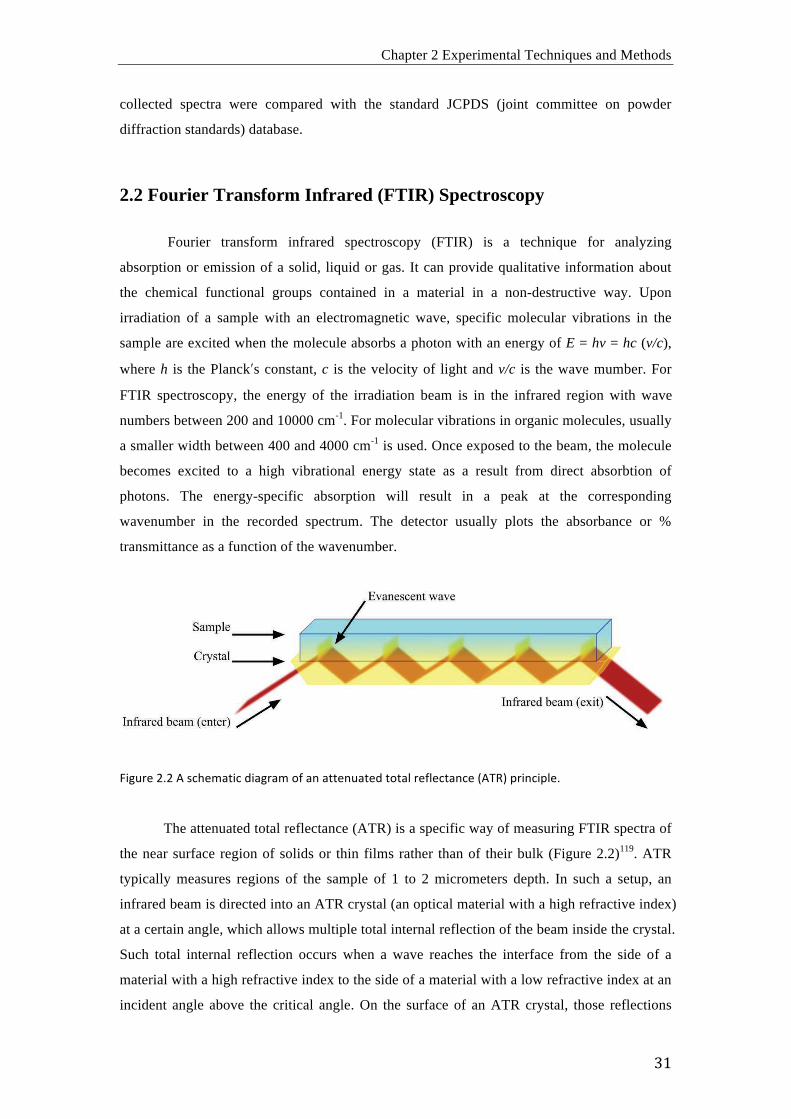
The attenuated total reflectance (ATR) is a specific way of measuring FTIR spectra of
the near surface region of solids or thin films rather than of their bulk (Figure 2.2)119. ATR
typically measures regions of the sample of 1 to 2 micrometers depth. In such a setup, an
infrared beam is directed into an ATR crystal (an optical material with a high refractive index)
at a certain angle, which allows multiple total internal reflection of the beam inside the crystal.
Such total internal reflection occurs when a wave reaches the interface from the side of a
material with a high refractive index to the side of a material with a low refractive index at an
incident angle above the critical angle. On the surface of an ATR crystal, those reflections
Chapter 2 Experimental Techniques and Methods
32
will form an evanescent wave. If at the interface the sample is positioned, the evanescent
waves are attenuated or altered after penetrating into and interacting with the sample. The
attenuated evanescent wave is passed back to the IR beam, exits the ATR crystal and is
finally collected by the detector. The recorded signal contains information about the sample
fraction in near vicinity of the ATR crystal.
In this thesis, all FTIR measurements were performed with a Fourier Transform
Infrared (FTIR) spectrometer (FT-IR spectrometer Frontier, PerkinElmer) equipped with an
ATR setup. All samples were prepared as thin films by drop casting their solutions onto
silicon wafers or glass substrates.
2.3 Raman Spectroscopy
Raman spectroscopy is a technique that allows to identify vibrational, rotational and
other low frequency modes in a material system120. Raman spectroscopy is complementary to
FTIR and is commonly used in chemistry to provide a fingerprint by which molecules can be
identified. It relies on inelastic scattering (raman scattering) of monochromatic light, usually
emitted by a laser in the visible, near infrared, or near ultraviolet range. For obtaining Raman
spectra, the sample is commonly illuminated with a laser beam in visible range. The molecule
absorbs photons with frequency v1 and becomes excited to a high virtual energy state. Some
of the molecules relax back to the initial energy state by emitting photons with the same
frequency v1, while others relax to another vibrational energy state by emitting photons with
further frequencies vi. The photons with frequency vi are recorded and stand in relation to the
molecular vibrational frequencies.
In this work, Raman spectroscopy was carried out in a Raman microscope (Alpha
300S, WITec), with a light source at a wavelength of 532 nm (100× objective). The Raman
spectra were background corrected and obtained by averaging spectra from five different
regions of each sample. The collected data were analyzed with the WIT spectra software.
2.4 Electron Microscopy (SEM and TEM)
The resolution of an optical microscope is limited to about 200 nm depending on the
wavelength of the used visible light. In order to achieve higher resolutions, further sources of
illumination are needed. The electron microscope uses a beam of accelerated electrons as a
source of illumination, which allows for investigation of the ultrastructure of a wide range of
biological and inorganic specimens including microorganisms, cells, large molecules, metals,
and crystals. The electron microscope can span magnifications ranging from thousands to
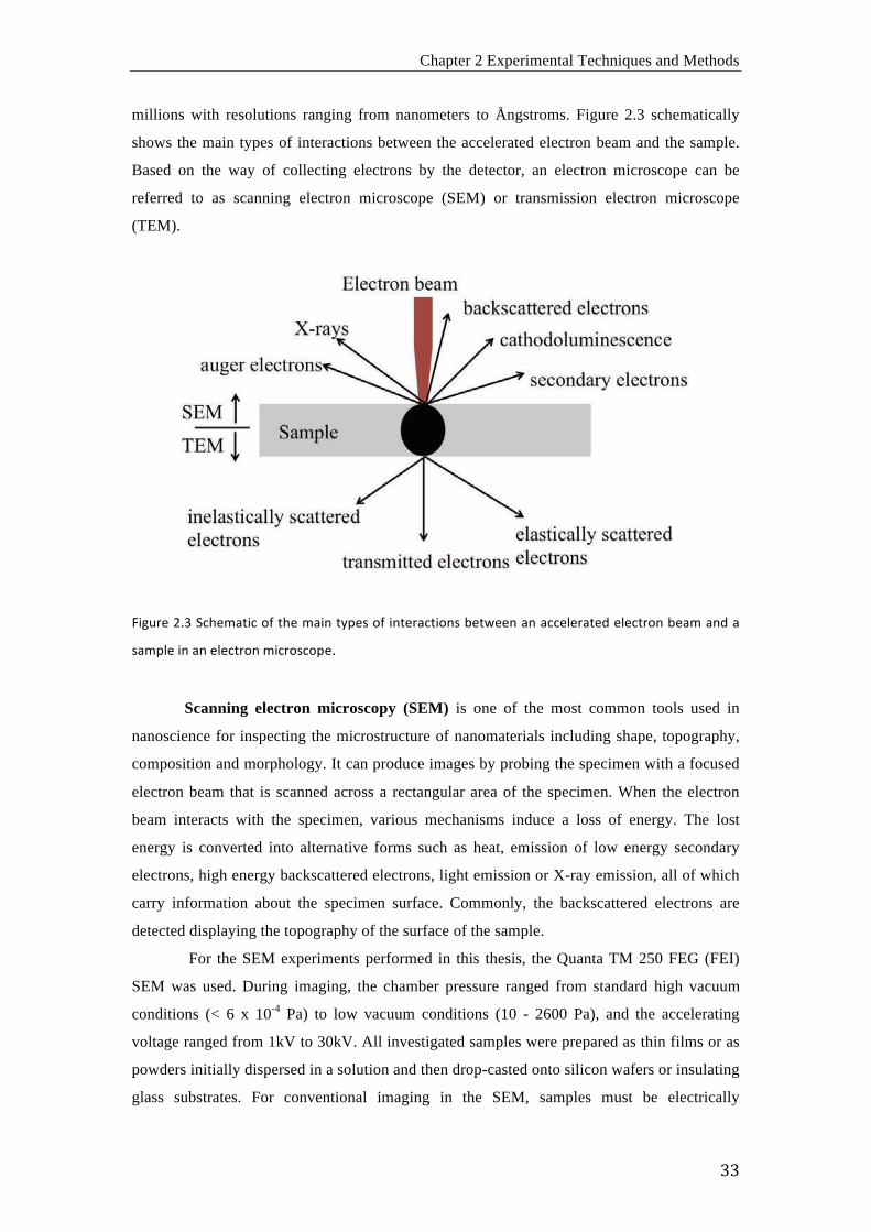
Chapter 2 Experimental Techniques and Methods
''!
millions with resolutions ranging from nanometers to Ångstroms. Figure 2.3 schematically
shows the main types of interactions between the accelerated electron beam and the sample.
Based on the way of collecting electrons by the detector, an electron microscope can be
referred to as scanning electron microscope (SEM) or transmission electron microscope
(TEM).
L<M"#,'UHQ'>;[,E%G<;'8O'G[,'E%<='GCB,&'8O'<=G,#%;G<8=&'D,G\,,='%='%;;,6,#%G,+',6,;G#8='D,%E'%=+'%'
&%EB6,'<='%=',6,;G#8='E<;#8&;8B,.
Scanning electron microscopy (SEM) is one of the most common tools used in
nanoscience for inspecting the microstructure of nanomaterials including shape, topography,
composition and morphology. It can produce images by probing the specimen with a focused
electron beam that is scanned across a rectangular area of the specimen. When the electron
beam interacts with the specimen, various mechanisms induce a loss of energy. The lost
energy is converted into alternative forms such as heat, emission of low energy secondary
electrons, high energy backscattered electrons, light emission or X-ray emission, all of which
carry information about the specimen surface. Commonly, the backscattered electrons are
detected displaying the topography of the surface of the sample.
For the SEM experiments performed in this thesis, the Quanta TM 250 FEG (FEI)
SEM was used. During imaging, the chamber pressure ranged from standard high vacuum
conditions (< 6 x 10⁻⁴ Pa) to low vacuum conditions (10 - 2600 Pa), and the accelerating
voltage ranged from 1kV to 30kV. All investigated samples were prepared as thin films or as
powders initially dispersed in a solution and then drop-casted onto silicon wafers or insulating
glass substrates. For conventional imaging in the SEM, samples must be electrically
Chapter 2 Experimental Techniques and Methods
34
conductive, at least at the surface, and electrically grounded to prevent the accumulation of
electrostatic charge. Non-conducting materials are usually coated with an ultrathin coating of
electrically conducting material, such as carbon or platinum, deposited on the sample either
by low-vacuum sputter coating or by high-vacuum thermal evaporation.
Transmission electron microscopy (TEM), the original form of electron
microscopy, uses a high voltage electron beam to illuminate the specimen and enables
collecting information from transmitted electons to create an image. The resolution is
typically about an order of magnitude better than that in a typical SEM. From the TEM
images, crystalline lattices of materials and even single atoms can be observed, provided good
alignment of the instrument is done.
Energy-dispersive X-ray spectroscopy (EDS), is an analytical technique used for the
elemental analysis of a sample. To stimulate the emission of characteristic X-rays from a
specimen, a high-energy beam of charged particles, such as electrons or protons, is focused
on the sample. The beam will excite an electron from an inner shell, ejecting it from the shell
while an electron hole will be left behind. This hole will be filled with an electron from an
outer shell, and the difference in energy between the outer and the inner shell will be released
in form of X-ray irradiation. The number and energy of the X-rays emitted from a specimen
are measured by an energy-dispersive spectrometer. As the energies of X-rays are
characteristic of the difference in energy between two shells and the atomic structure of the
emitting atom, EDS allows precise determination of the elemental composition of a specimen.
In all experiments performed in this thesis, a Helios NanoLab Dual Beam (FEI, NL)
was used to examine samples in scanning transmission mode. TEM imaging and EDS
analysis were carried out with an FEI Titan microscope operating at 300 kV acceleration
voltage in STEM mode and equipped with an EDAX SDD detector.
2.5 Ultraviolet -Visible Spectroscopy
Ultraviolet-Visible Spectroscopy (UV-Vis) refers to absorption spectroscopy or
reflectance spectroscopy in the ultraviolet-visible spectral region. The absorption or
reflectance in the visible range directly affects the perceived color of the chemicals involved.
In this region of the electromagnetic spectrum, atoms and molecules undergo electronic
transitions. The absorption spectroscopy characterizes transitions of molecules from the
ground state to the excited state121. The wavelengths of the absorption peaks can be correlated
with the types of bonds in a given molecule and are valuable for determining the functional
groups contained in a molecule.
Chapter 2 Experimental Techniques and Methods
35
For the Uv-vis experiments performed in this thesis, all samples were prepared as thin
films initially dispersed in a solution and then drop-casted onto insulating glass substrates.
Absorption spectra of the samples were recorded between 250-890 nm using a UV-Vis
spectrophotometer (V-630 BIO, JASCO).
2.6 Atomic Force Microscopy (AFM) Atomic-force microscopy (AFM) is scanning probe microscopy technique, commonly
used to characterize the surface structure and morphology of materials. During AFM probing,
information about the morphology of a sample is gathered by ¨feeling¨ or ¨touching¨ the
surface with a mechanical probe or tip. Piezoelectric elements facilitate tiny but accurate and
precise lateral movements of tip or sample. The cantilever, to which the tip is attached, is
vertically deflected during the measurement due to attractive and repulsive forces between the
tip and the sample surface. Focusing a laser onto the cantilever and recording the movement
of the reflected laser with a photodiode while scanning the sample allows for a visual
reconstruction of the sample morphology.
AFM can be used in three distinct modes: contact mode, also called static mode,
tapping mode, also called intermittent contact mode, and non-contact mode. Among those the
tapping mode is the most frequently used AFM mode when operating in ambient conditions.
In tapping mode, the cantilever oscillates up and down near its resonance frequency at a
constant amplitude122. When the tip comes close to the surface, interactions between the tip
and the sample surface cause the oscillation amplitude of the cantilever to change. This
change of the amplitude is used as feedback to readjust the distance of the cantilever to the
sample with a piezo crystal. Due to the intermittent contact of the tip with the sample surface,
negligible damage to the sample is induced.
In this thesis, AFM analysis was performed on P3HT polymer-coated glass slides,
employing a 5500 AFM (Keysight, Santa Clara).
2.7 X-ray Photoelectron Spectroscopy (XPS)
X-ray photoelectron spectroscopy (XPS) is a surface-sensitive quantitative
spectroscopic technique that is commonly used to analyze elemental compositions, chemical
states and electronic states of the elements that are present in a material. In XPS, the sample is
irradiated with a beam of X-rays under high vacuum (P ∼ 10-8 millibar) or ultra high vacuum
(UHV; P < 10-9 millibar) conditions. The X-ray beam can penetrate into the sample and
Chapter 2 Experimental Techniques and Methods
36
interact with the electrons. After absorbing energy from the X-ray beam, the near-surface
electrons are excited, leading to an escape from the sample. The kinetic energy and number of
the escaped electrons are analyzed by a detector. Because the energy of the used X-ray with
particular wavelength is known (for Al Kα X-rays, Ephoton = 1486.7 eV), and because the
emitted electrons' kinetic energies are measured, the binding energy of each of the emitted
electrons can be determined by using an equation that is based on the equation of Ernest
Rutherford:
Ebinding = Ephoton − (Ekinetic + ϕ),
where Ebinding is the binding energy (BE) of the electrons, Ephoton is the energy of the X-ray
photons being used, Ekinetic is the kinetic energy of the electron as measured by the instrument
and ϕ is the work function dependent on both the spectrometer and the material and is
normally constant in practice. This equation describes essentially the conservation of energy
equation. The work function term ϕ is an adjustable instrumental correction factor that
accounts for the few eV of kinetic energy given up by the photoelectron as it becomes
absorbed by the instrument's detector. It is a constant that rarely needs to be adjusted in
practice. The binding energy of recorded electrons depends on their origin, which allows
identifying the specific atoms, neighboring atoms and specific orbitals. A quantitative
analysis can be obtained by analyzing the intensity of the recorded photoelectrons.
Importantly, XPS is a surface sensitive spectroscopic technique, because only the electrons
within an area of several nanometers close to the surface can escape from the sample and be
recorded.
XPS experiments in this thesis were conducted using a Phoibos photoelectron
spectrometer equipped with an Al Kα X-ray source (12 mA, 8.33 kV) as the incident photon
radiation. All samples were drop-casted onto silicon substrates. The spectra were standardized
using the C 1s peak at 284.6 eV. The base pressure of the UHV chamber was maintained at
10-9-10-10 mbar.
2.8 Assessment of the Electrical Conductivity Electrical conductivity of a material is a measure of its ability to conduct electric
current under certain conditions, such as temperature, pressure, applied current, and so on.
From the simple Ohm,s law on conductivity (V=R × I; where V is the voltage, I is the current,
and R is the resistance), it is obvious that a measurement of R may simply be done by
applying a current (I) and measuring a potential (V). Since R depends on geometrical
parameters (and therefore is sample dependent) the magnitude usually given is the resistivity
(ρ), which is defined as ρ = R × (A/l), where A is the cross-sectional area of the conductor (A=
Chapter 2 Experimental Techniques and Methods
37
a × d; a is the width, and d is the thickness of the sample) and l is the distance between the
voltage-drop measuring points123. For historical reasons the resistivity is usually measured in
Ω cm instead of Ω m. Besides the resistivity, the other magnitude that is usually provided is
its inverse, called the conductivity, σ = (1/ ρ), which is measured in Ω-1 cm-1 = S cm-1 (Ω-1 = S
= Siemens). This conductivity σ is used in the present thesis. The simplest way to measure
electrical conductivity is to send a constant current through two electrical probes, and sense
the voltage between the probes. However, the two-probe method acquires the total resistance
of the circuit, including the contact resistance, the probe resistance, and the spreading
resistances under the probes. This analysis makes an individual assessment of the sample
resistance very difficult.
The four point probe method is the most common method to determine electrical
conductivity without influence of the above mentioned contributions124,125. This method uses
an additional pair of probes to separately sense voltage with a high impedance voltmeter, so
that the parasitic resistances mentioned above are negligible since virtually no current flows
between the voltage probe pairs. During the conductivity testing processes of thin films, all
four probes are positioned on the surface of the film. Figure 2.4 illustrates various four-probe
configurations for thin film measurements. As shown in Figure 2.4 (a), collinear four-point
probes with equal spacing can be put in contact with the sample surface. If the sample size is
larger than the probe spacing and the thickness of the film is less than a half of probe spacing,
one can obtain the electrical conductivity σ of the film by124
σ = ln2 I/πd V,
where I is the current, V is the voltage and the d is the thickness of the sample.
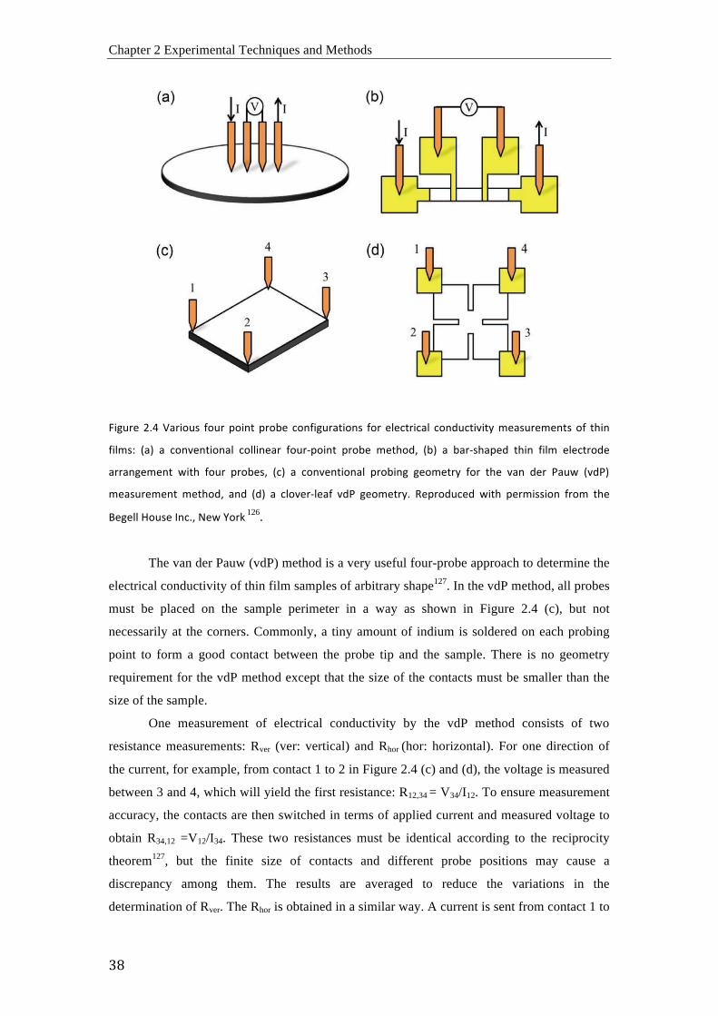
Chapter 2 Experimental Techniques and Methods
'.!
L<M"#,'UH?'*%#<8"&' O8"#'B8<=G'B#8D,' ;8=O<M"#%G<8=&' O8#' ,6,;G#<;%6' ;8=+";G<$<GC'E,%&"#,E,=G&'8O' G[<='
O<6E&`' -%.' %' ;8=$,=G<8=%6' ;866<=,%#' O8"#)B8<=G' B#8D,' E,G[8+7' -D.' %' D%#)&[%B,+' G[<=' O<6E' ,6,;G#8+,'
%##%=M,E,=G' \<G[' O8"#' B#8D,&7' -;.' %' ;8=$,=G<8=%6' B#8D<=M' M,8E,G#C' O8#' G[,' $%=' +,#' /%"\' -$+/.'
E,%&"#,E,=G' E,G[8+7' %=+' -+.' %' ;68$,#)6,%O' $+/' M,8E,G#CH a,B#8+";,+' \<G[' B,#E<&&<8=' O#8E' G[,'
d,M,66'58"&,'(=;H7'1,\'h8#_'126.
The van der Pauw (vdP) method is a very useful four-probe approach to determine the
electrical conductivity of thin film samples of arbitrary shape127. In the vdP method, all probes
must be placed on the sample perimeter in a way as shown in Figure 2.4 (c), but not
necessarily at the corners. Commonly, a tiny amount of indium is soldered on each probing
point to form a good contact between the probe tip and the sample. There is no geometry
requirement for the vdP method except that the size of the contacts must be smaller than the
size of the sample.
One measurement of electrical conductivity by the vdP method consists of two
resistance measurements: Rver (ver: vertical) and Rhor (hor: horizontal). For one direction of
the current, for example, from contact 1 to 2 in Figure 2.4 (c) and (d), the voltage is measured
between 3 and 4, which will yield the first resistance: R12,34 = V34/I12. To ensure measurement
accuracy, the contacts are then switched in terms of applied current and measured voltage to
obtain R34,12 =V12/I34. These two resistances must be identical according to the reciprocity
theorem127, but the finite size of contacts and different probe positions may cause a
discrepancy among them. The results are averaged to reduce the variations in the
determination of Rver. The Rhor is obtained in a similar way. A current is sent from contact 1 to
Chapter 2 Experimental Techniques and Methods
39
the other adjacent contact 4, and the voltage between 2 and 3 is measured to gain R14,23 =
V23/I14. Again, R23,14 = V14/I23 is also aquired. Rhor is then obtained from the average of R14,23
and R23,14. It is sometimes desirable to reverse the current polarity and /or measure several
voltages generated from varying magnitudes of current to eliminate parasitic voltages that
may be present during the measurement. Combining these two resistances in the vdP formula,
one can calculate the electrical conductivity σ of the sample with the following equation,
1𝜎=𝜋𝑑ln 2
𝑅𝑣𝑒𝑟 + 𝑅ℎ𝑜𝑟
2 𝑓
𝑅𝑣𝑒𝑟𝑅ℎ𝑜𝑟
where f is a function of the resistance ratio, d is the film thickness.
In this work, the conductivities of the thin films were measured applying the collinear
four-point probe technique with a source measurement unit (Keithley 2611). For each VPI
experiment 5 or 6 individual samples were tested for each VPI cycle number. The resulting
conductivity σ was calculated according to the formula,
σ = ln2 I/πd V.
where I is the current, V is the voltage and the d is the thickness of the polymer film.

Chapter 2 Experimental Techniques and Methods
40
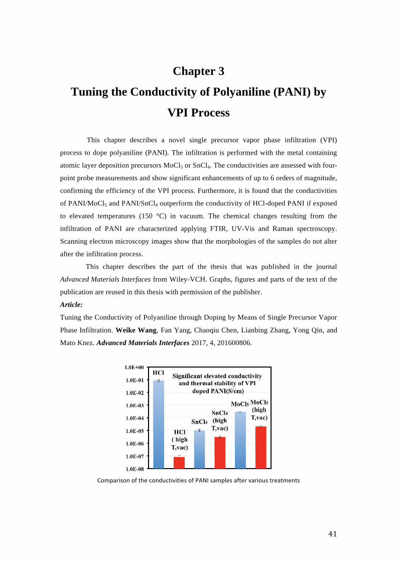
!!
,&!
Chapter 3
Tuning the Conductivity of Polyaniline (PANI) by
VPI Process
This chapter describes a novel single precursor vapor phase infiltration (VPI)
process to dope polyaniline (PANI). The infiltration is performed with the metal containing
atomic layer deposition precursors MoCl5 or SnCl4. The conductivities are assessed with four-
point probe measurements and show significant enhancements of up to 6 orders of magnitude,
confirming the efficiency of the VPI process. Furthermore, it is found that the conductivities
of PANI/MoCl5 and PANI/SnCl4 outperform the conductivity of HCl-doped PANI if exposed
to elevated temperatures (150 °C) in vacuum. The chemical changes resulting from the
infiltration of PANI are characterized applying FTIR, UV-Vis and Raman spectroscopy.
Scanning electron microscopy images show that the morphologies of the samples do not alter
after the infiltration process.
This chapter describes the part of the thesis that was published in the journal
Advanced Materials Interfaces from Wiley-VCH. Graphs, figures and parts of the text of the
publication are reused in this thesis with permission of the publisher.
Article:
Tuning the Conductivity of Polyaniline through Doping by Means of Single Precursor Vapor
Phase Infiltration. Weike Wang, Fan Yang, Chaoqiu Chen, Lianbing Zhang, Yong Qin, and
Mato Knez. Advanced Materials Interfaces 2017, 4, 201600806.
!8EB%#<&8='8O'G[,';8=+";G<$<G<,&'8O'/01('&%EB6,&'%OG,#'$%#<8"&'G#,%GE,=G&'

Chapter 3 Vapor Phase Infiltration of Polyaniline (PANI)
42
Chapter 3 Vapor Phase Infiltration of Polyaniline (PANI)
43
3.1. Introduction
Conductive polymers are subject of research since several decades, but their promise
as functional material in flexible electronics seriously intensified the research effort on those
materials during the past years. Improvement of the conductivity and chemical or thermal
stability of a conductive polymer will allow beneficial substitution of inorganic materials in a
broad range of electronic devices, including thin-film transistors128, light emitting diodes129,
solar cells130, batteries131, or supercapacitors132. With its highly conjugated π delocalized
molecular backbone, polyaniline (PANI) belongs to the most prominent organic
semiconductors and acts as model system for many further conductive polymers. With view
on its application potential, very promising results have been demonstrated in a variety of
application fields including sensors, actuators, antistatic coatings, corrosion protection,
rechargeable batteries, microwave absorption and electro-optic and electrochromic
devices25,133. The level of conductivity of PANI is of crucial importance for most of the
applications and depends on the switching between the different states of the polymer, namely,
leucoemeraldine, emeraldine, and pernigraniline states, as a response to a chemical or
electrical trigger. The conductivity of PANI can be altered by doping and inorganic protonic
acids134,135, organic acids136,137, alkali metal salts138,139, Lewis acids140,141, and transition metal
salts 142,143 are the most commonly used dopants. Usually, the doping relies on wet chemistry,
which not only introduces impurities into the PANI by inclusion of solvent molecules or
additives, but also severely influences the morphology and structure of PANI as such
additives impact the polymerization or crystallization of the material. This is very often
considered to be a serious drawback for shaping the polymer for various applications. A
promising approach to avoid such negative influence from the solvents and obtain better
control of the doping process may lie in the vacuum-based processing. In fact, atomic layer
deposition (ALD) and related vapor phase infiltration (VPI) strategies take advantage of the
mobility of a vaporized chemical to diffuse into and react with polymeric substrates88, which
may be very beneficial for a solvent-free and controllable doping process.
Incorporation of inorganic materials into polymers often enhances the mechanical,
optical, or electronic properties of the resulting composite or hybrid material110-114. For
example, in our earlier works we have demonstrated that infiltration of metal oxides or metal
ions into various (bio)polymers, including spider silk98, avian egg collagen107and cellulose109
by means of ALD-derived strategies often enhances their mechanical properties. In the
present work, we demonstrate that a similar infiltration process can also be used for doping
PANI. The strategy further allows for controlling the level of conductivity of the polymer
through the number of infiltration cycles applied. After doping with metal chlorides, the
Chapter 3 Vapor Phase Infiltration of Polyaniline (PANI)
44
doped PANI shows exceptional conductivity values, particularly at elevated temperatures,
indicating a significant difference in the physics and chemistry of the material in comparison
to PANI doped in a traditional way. On the example of two different ALD precursors, MoCl5
and SnCl4, we demonstrate that the conductivities of the resulting PANI/MoCl5 and
PANI/SnCl4 are superior to those of PANI doped with 1M HCl after exposure to elevated
temperatures (150 °C). This method may serve as complementary route for stabilizing
conductive PANI for high-temperature applications while avoiding the use of solvents and
making purification steps obsolete.
3.2. Experimental Section
3.2.1 Preparation the Polyaniline (PANI) nanofibers Thin Film
The synthesis of PANI nanofibers was carried out by a rapid mixing polymerization as
reported in literature135. All chemicals were analytical grade and were used as received.
Typically, an aqueous solution of aniline (3.2 mmol) in HCl (1 M, 10 mL) and a solution of
ammonium peroxydisulfate (0.8 mmol) in HCl (1 M, 10 mL) were prepared. The two
solutions were mixed at room temperature and rapid and immediate shaking ensured efficient
mixing. After 12 h polymerization time, the resulting HCl (1 M) doped PANI was collected
by filtration and washed several times with HCl (1 M) until the filtrate became colorless. At
last, it was dried in vacuum at 50 °C. De-doped PANI was obtained upon treatment of the
PANI/1M HCl with aqueous ammonium hydroxide (0.1 M) for 1 h and subsequent washing
with deionized water until the filtrate became pH-neutral, and finally dried in vacuum at
60 °C. Glass substrates (1.3×1.3 cm2) were cleaned in sequence with acetone, deionized water
(DI), and isopropanol, and subsequently dried in an oven overnight. PANI and PANI/1M HCl
films were coated (200 µL) on the glass substrates and the samples were dried in an oven at
60 °C for 12 h. In advance of the infiltration experiments, the de-doped PANI films were
stored overnight at 120 °C.
3.2.2 Vapor Phase Infiltration Process of PANI Thin Film
Vapor-phase infiltration was performed using a homemade atomic layer deposition
tool. De-doped PANI films on glass substrates were exposed to vapors of SnCl4 (Sigma, 98%)
or MoCl5 (Sigma, 95%) in a pulse-exposure-purge sequence with varied numbers of repetition
cycles. One cycle of the process consisted of following settings: the precursors were pulsed
Chapter 3 Vapor Phase Infiltration of Polyaniline (PANI)
45
into the reaction chamber for 0.1 s (SnCl4) or 5 s (MoCl5) and exposure of the substrates to
the vapors in the reaction chamber was allowed for 120 s. The exposure was followed by a 60
s purge step. The cycle was repeated with the number of cycles varying between 10 and 200.
As carrier and purging gas N2 (99.99%) was used. The reaction temperature was 150 °C, and
the base pressure of the reactor was ∼50 mTorr. Since at room temperature MoCl5 is solid,
heating of that precursor to 85 °C was required to obtain reasonable vapor pressure.
3.2.3 Characterization
Infrared spectra of the samples were recorded between 700 and 1800 cm-1 with a FTIR
Spectrometer (Frontier; PerkinElmer).
The morphology of the samples was characterized by scanning electron microscopy
(SEM, Quanta 250 FEG; FEI) and the composition analysis was done by energy-dispersive
X-ray spectroscopy (EDS). Thickness measurements were carried out on a cleaved cross-
section of the sample by FEG-SEM.
Raman spectra at 532 nm excitation wavelength were collected with a Raman
microscope (Alpha 300S, WITec). The laser power was kept below 0.7 mW to avoid sample
degradation.
Absorption spectra of the samples were recorded between 250-880 nm using a UV-vis
spectrophotometer (V-630 BIO, JASCO).
The conductivities of the films were measured applying a four-point probe technique
with a source measurement unit (Keithley 2611). For each experiment four or five individual
samples were tested for each VPI process cycle number. The resulting conductivity, was
calculated according to the formula,
where I is the current, V is the voltage and d is the film thickness.
)( VI d/2ln πσ =
Chapter 3 Vapor Phase Infiltration of Polyaniline (PANI)
46
3.3 Results and Discussion
3.3.1 Assessment of the electrical conductivity
Figure 3.1 I-‐V plots of (a) PANI/1M HCl, PANI/MoCl5 (100 cycles) and PANI/SnCl4 (60 cycles) as
prepared and (b) PANI/1M HCl, PANI/MoCl5 (100 cycles) and PANI/SnCl4 (60 cycles) after storage at
150°C in vacuum for 100 min. The inset shows the low current range area of Figure 1b. Conductivities
of (c) MoCl5 and (d) SnCl4 as a function of the number of infiltration cycles (measured at room
temperature). (e) Conductivity comparison of PANI/1M HCl, PANI/SnCl4 (60 cycles) and PANI/MoCl5
(100 cycles) as prepared, and after storage at 150 °C in vacuum for 100 min.
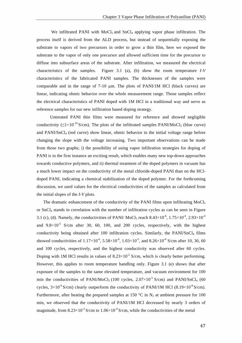
Chapter 3 Vapor Phase Infiltration of Polyaniline (PANI)
47
We infiltrated PANI with MoCl5 and SnCl4 applying vapor phase infiltration. The
process itself is derived from the ALD process, but instead of sequentially exposing the
substrate to vapors of two precursors in order to grow a thin film, here we exposed the
substrate to the vapor of only one precursor and allowed sufficient time for the precursor to
diffuse into subsurface areas of the substrate. After infiltration, we measured the electrical
characteristics of the samples. Figure 3.1 (a), (b) show the room temperature I-V
characteristics of the fabricated PANI samples. The thicknesses of the samples were
comparable and in the range of 7-10 µm. The plots of PANI/1M HCl (black curves) are
linear, indicating ohmic behavior over the whole measurement range. Those samples reflect
the electrical characteristics of PANI doped with 1M HCl in a traditional way and serve as
reference samples for our new infiltration based doping strategy.
Untreated PANI thin films were measured for reference and showed negligible
conductivity (≤1×10⁻¹⁰ S/cm). The plots of the infiltrated samples PANI/MoCl5 (blue curve)
and PANI/SnCl4 (red curve) show linear, ohmic behavior in the initial voltage range before
changing the slope with the voltage increasing. Two important observations can be made
from those two graphs; i) the possibility of using vapor infiltration strategies for doping of
PANI is in the first instance an exciting result, which enables many new top-down approaches
towards conductive polymers, and ii) thermal treatment of the doped polymers in vacuum has
a much lower impact on the conductivity of the metal chloride-doped PANI than on the HCl-
doped PANI, indicating a chemical stabilization of the doped polymer. For the forthcoming
discussion, we used values for the electrical conductivities of the samples as calculated from
the initial slopes of the I-V plots.
The dramatic enhancement of the conductivity of the PANI films upon infiltrating MoCl5
or SnCl4 stands in correlation with the number of infiltration cycles as can be seen in Figure
3.1 (c), (d). Namely, the conductivities of PANI/ MoCl5 reach 8.43×10⁻⁶, 1.75×10⁻⁴, 2.93×10⁻⁴
and 9.8×10⁻⁵ S/cm after 30, 60, 100, and 200 cycles, respectively, with the highest
conductivity being obtained after 100 infiltration cycles. Similarly, the PANI/SnCl4 films
showed conductivities of 1.17×10⁻⁶, 5.58×10⁻⁶, 1.03×10⁻⁵, and 8.26×10⁻⁶ S/cm after 10, 30, 60
and 100 cycles, respectively, and the highest conductivity was observed after 60 cycles.
Doping with 1M HCl results in values of 8.23×10⁻² S/cm, which is clearly better performing.
However, this applies to room temperature handling only. Figure 3.1 (e) shows that after
exposure of the samples to the same elevated temperature, and vacuum environment for 100
min the conductivities of PANI/MoCl5 (100 cycles, 2.07×10⁻⁵ S/cm) and PANI/SnCl4 (60
cycles, 3×10⁻⁶ S/cm) clearly outperform the conductivity of PANI/1M HCl (8.19×10⁻⁸ S/cm).
Furthermore, after heating the prepared samples at 150 °C in N2 at ambient pressure for 100
min, we observed that the conductivity of PANI/1M HCl decreased by nearly 3 orders of
magnitude, from 8.23×10⁻² S/cm to 1.06×10⁻⁴ S/cm, while the conductivities of the metal
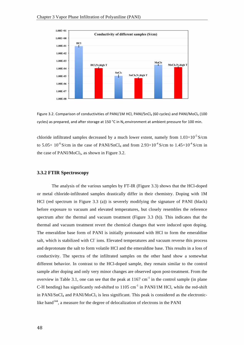
Chapter 3 Vapor Phase Infiltration of Polyaniline (PANI)
48
Figure 3.2. Comparison of conductivities of PANI/1M HCl, PANI/SnCl4 (60 cycles) and PANI/MoCl5 (100
cycles) as prepared, and after storage at 150 °C in N2 environment at ambient pressure for 100 min.
chloride infiltrated samples decreased by a much lower extent, namely from 1.03×10⁻⁵ S/cm
to 5.05× 10⁻⁶ S/cm in the case of PANI/SnCl4 and from 2.93×10⁻⁴ S/cm to 1.45×10⁻⁴ S/cm in
the case of PANI/MoCl5, as shown in Figure 3.2.
3.3.2 FTIR Spectroscopy
The analysis of the various samples by FT-IR (Figure 3.3) shows that the HCl-doped
or metal chloride-infiltrated samples drastically differ in their chemistry. Doping with 1M
HCl (red spectrum in Figure 3.3 (a)) is severely modifying the signature of PANI (black)
before exposure to vacuum and elevated temperatures, but closely resembles the reference
spectrum after the thermal and vacuum treatment (Figure 3.3 (b)). This indicates that the
thermal and vacuum treatment revert the chemical changes that were induced upon doping.
The emeraldine base form of PANI is initially protonated with HCl to form the emeraldine
salt, which is stabilized with Cl- ions. Elevated temperatures and vacuum reverse this process
and deprotonate the salt to form volatile HCl and the emeraldine base. This results in a loss of
conductivity. The spectra of the infiltrated samples on the other hand show a somewhat
different behavior. In contrast to the HCl-doped sample, they remain similar to the control
sample after doping and only very minor changes are observed upon post-treatment. From the
overview in Table 3.1, one can see that the peak at 1167 cm-1 in the control sample (in plane
C-H bending) has significantly red-shifted to 1105 cm-1 in PANI/1M HCl, while the red-shift
in PANI/SnCl4 and PANI/MoCl5 is less significant. This peak is considered as the electronic-
like band144, a measure for the degree of delocalization of electrons in the PANI
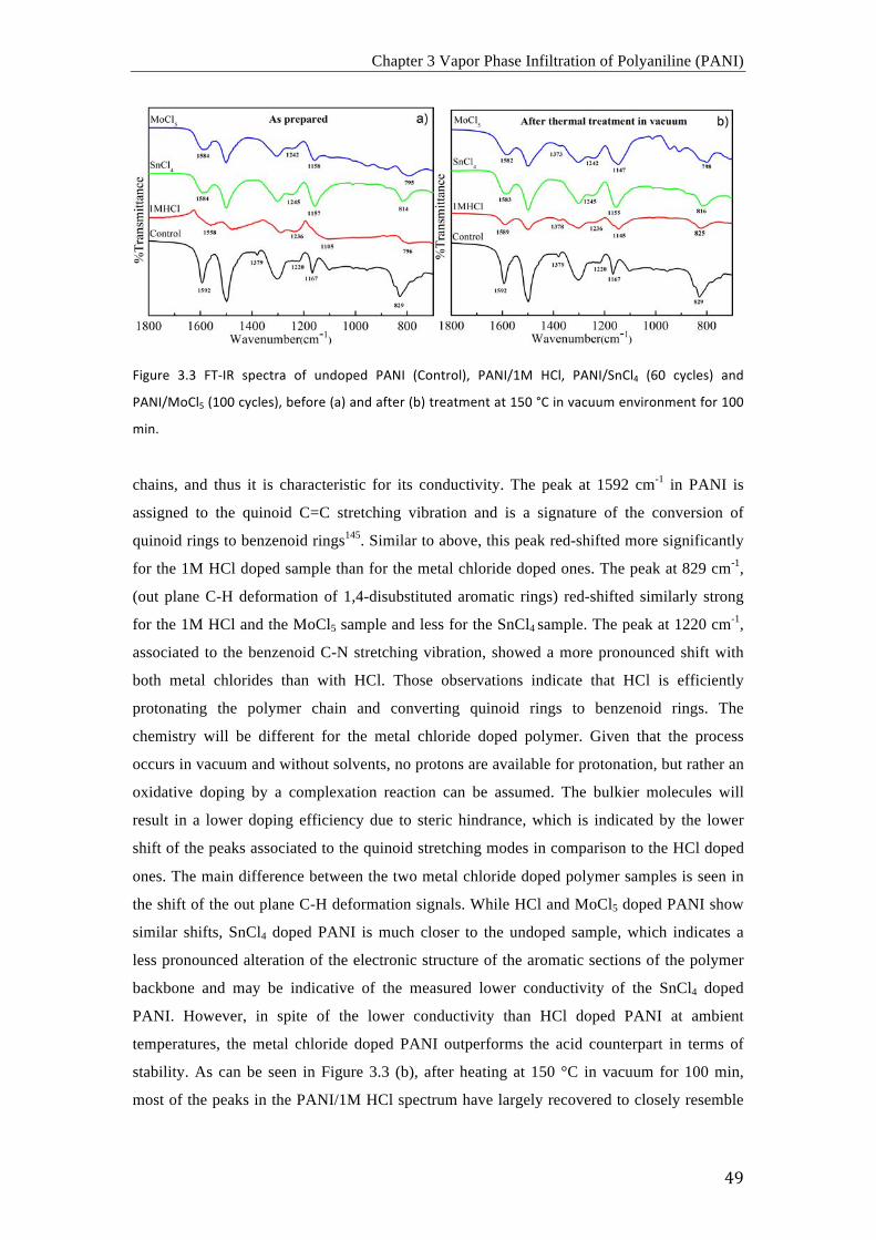
Chapter 3 Vapor Phase Infiltration of Polyaniline (PANI)
49
Figure 3.3 FT-‐IR spectra of undoped PANI (Control), PANI/1M HCl, PANI/SnCl4 (60 cycles) and
PANI/MoCl5 (100 cycles), before (a) and after (b) treatment at 150 °C in vacuum environment for 100
min.
chains, and thus it is characteristic for its conductivity. The peak at 1592 cm-1 in PANI is
assigned to the quinoid C=C stretching vibration and is a signature of the conversion of
quinoid rings to benzenoid rings145. Similar to above, this peak red-shifted more significantly
for the 1M HCl doped sample than for the metal chloride doped ones. The peak at 829 cm-1,
(out plane C-H deformation of 1,4-disubstituted aromatic rings) red-shifted similarly strong
for the 1M HCl and the MoCl5 sample and less for the SnCl4 sample. The peak at 1220 cm-1,
associated to the benzenoid C-N stretching vibration, showed a more pronounced shift with
both metal chlorides than with HCl. Those observations indicate that HCl is efficiently
protonating the polymer chain and converting quinoid rings to benzenoid rings. The
chemistry will be different for the metal chloride doped polymer. Given that the process
occurs in vacuum and without solvents, no protons are available for protonation, but rather an
oxidative doping by a complexation reaction can be assumed. The bulkier molecules will
result in a lower doping efficiency due to steric hindrance, which is indicated by the lower
shift of the peaks associated to the quinoid stretching modes in comparison to the HCl doped
ones. The main difference between the two metal chloride doped polymer samples is seen in
the shift of the out plane C-H deformation signals. While HCl and MoCl5 doped PANI show
similar shifts, SnCl4 doped PANI is much closer to the undoped sample, which indicates a
less pronounced alteration of the electronic structure of the aromatic sections of the polymer
backbone and may be indicative of the measured lower conductivity of the SnCl4 doped
PANI. However, in spite of the lower conductivity than HCl doped PANI at ambient
temperatures, the metal chloride doped PANI outperforms the acid counterpart in terms of
stability. As can be seen in Figure 3.3 (b), after heating at 150 °C in vacuum for 100 min,
most of the peaks in the PANI/1M HCl spectrum have largely recovered to closely resemble
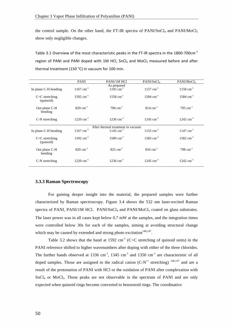
Chapter 3 Vapor Phase Infiltration of Polyaniline (PANI)
50
the control sample. On the other hand, the FT-IR spectra of PANI/SnCl4 and PANI/MoCl5
show only negligible changes.
Table 3.1 Overview of the most characteristic peaks in the FT-‐IR spectra in the 1800-‐700cm-‐1
region of PANI and PANI doped with 1M HCl, SnCl4 and MoCl5 measured before and after
thermal treatment (150 °C) in vacuum for 100 min.
PANI PANI/1M HCl PANI/SnCl4 PANI/MoCl5
As prepared In plane C-H bending 1167 cm-1 1105 cm-1 1157 cm-1 1158 cm-1
C=C stretching (quinoid)
1592 cm-1 1558 cm-1 1584 cm-1 1584 cm-1
Out plane C-H bending
829 cm-1 796 cm-1 814 cm-1 795 cm-1
C-N stretching 1220 cm-1 1236 cm-1 1245 cm-1 1242 cm-1
After thermal treatment in vacuum In plane C-H bending 1167 cm-1 1145 cm-1 1155 cm-1 1147 cm-1
C=C stretching (quinoid)
1592 cm-1 1589 cm-1 1583 cm-1 1582 cm-1
Out plane C-H bending
829 cm-1 825 cm-1 816 cm-1 798 cm-1
C-N stretching 1220 cm-1 1236 cm-1 1245 cm-1 1242 cm-1
3.3.3 Raman Spectroscopy
For gaining deeper insight into the material, the prepared samples were further
characterized by Raman spectroscopy. Figure 3.4 shows the 532 nm laser-excited Raman
spectra of PANI, PANI/1M HCl,PANI/SnCl4 and PANI/MoCl5 coated on glass substrates.
The laser power was in all cases kept below 0.7 mW at the samples, and the integration times
were controlled below 30s for each of the samples, aiming at avoiding structural change
which may be caused by extended and strong photo excitation146,147.
Table 3.2 shows that the band at 1592 cm-1 (C=C stretching of quinoid units) in the
PANI reference shifted to higher wavenumbers after doping with either of the three chlorides.
The further bands observed at 1336 cm-1, 1345 cm-1 and 1350 cm-1 are characteristic of all
doped samples. Those are assigned to the radical cation (C-N+• stretching) 146,147 and are a
result of the protonation of PANI with HCl or the oxidation of PANI after complexation with
SnCl4 or MoCl5. Those peaks are not observable in the spectrum of PANI and are only
expected when quinoid rings become converted to benzenoid rings. The coordinative
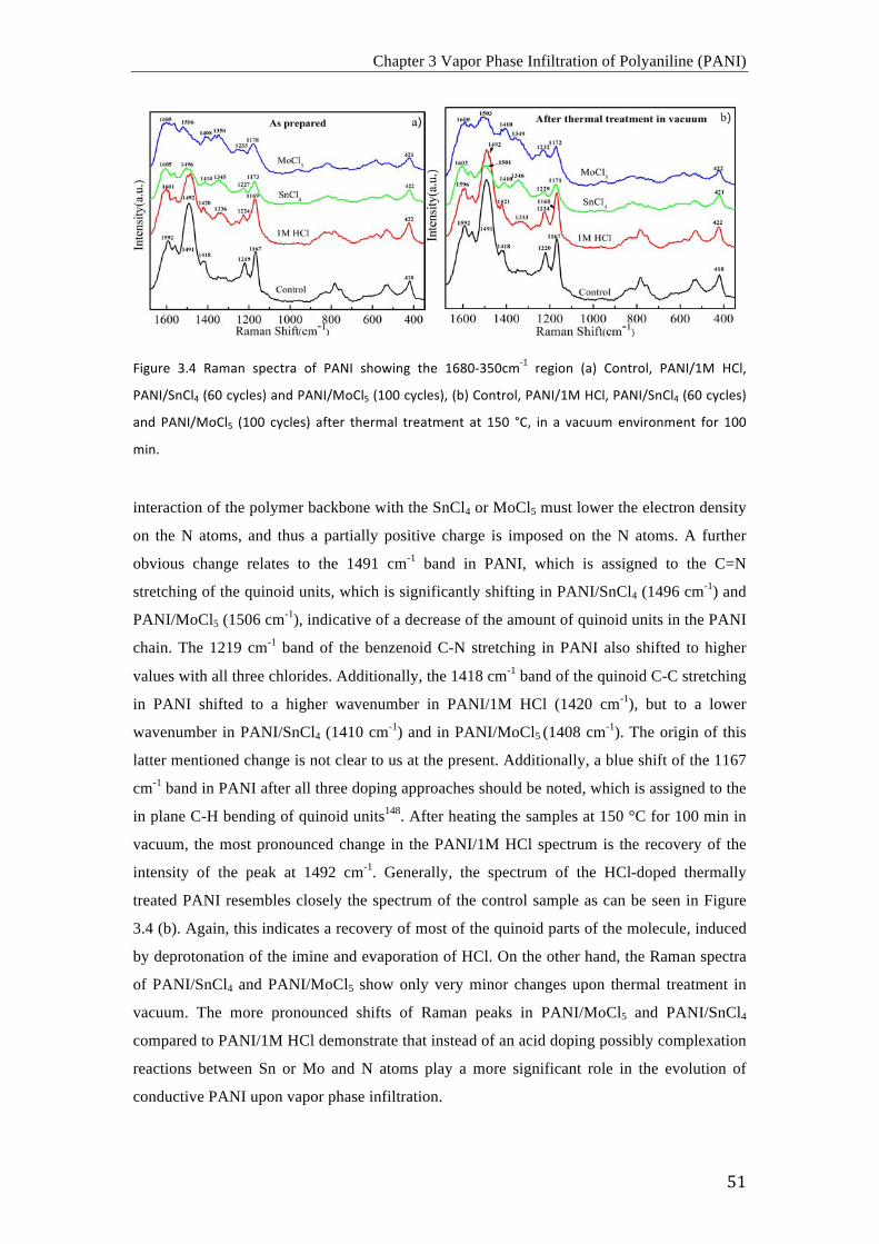
Chapter 3 Vapor Phase Infiltration of Polyaniline (PANI)
51
Figure 3.4 Raman spectra of PANI showing the 1680-‐350cm-‐1 region (a) Control, PANI/1M HCl,
PANI/SnCl4 (60 cycles) and PANI/MoCl5 (100 cycles), (b) Control, PANI/1M HCl, PANI/SnCl4 (60 cycles)
and PANI/MoCl5 (100 cycles) after thermal treatment at 150 °C, in a vacuum environment for 100
min.
interaction of the polymer backbone with the SnCl4 or MoCl5 must lower the electron density
on the N atoms, and thus a partially positive charge is imposed on the N atoms. A further
obvious change relates to the 1491 cm-1 band in PANI, which is assigned to the C=N
stretching of the quinoid units, which is significantly shifting in PANI/SnCl4 (1496 cm-1) and
PANI/MoCl5 (1506 cm-1), indicative of a decrease of the amount of quinoid units in the PANI
chain. The 1219 cm-1 band of the benzenoid C-N stretching in PANI also shifted to higher
values with all three chlorides. Additionally, the 1418 cm-1 band of the quinoid C-C stretching
in PANI shifted to a higher wavenumber in PANI/1M HCl (1420 cm-1), but to a lower
wavenumber in PANI/SnCl4 (1410 cm-1) and in PANI/MoCl5 (1408 cm-1). The origin of this
latter mentioned change is not clear to us at the present. Additionally, a blue shift of the 1167
cm-1 band in PANI after all three doping approaches should be noted, which is assigned to the
in plane C-H bending of quinoid units148. After heating the samples at 150 °C for 100 min in
vacuum, the most pronounced change in the PANI/1M HCl spectrum is the recovery of the
intensity of the peak at 1492 cm-1. Generally, the spectrum of the HCl-doped thermally
treated PANI resembles closely the spectrum of the control sample as can be seen in Figure
3.4 (b). Again, this indicates a recovery of most of the quinoid parts of the molecule, induced
by deprotonation of the imine and evaporation of HCl. On the other hand, the Raman spectra
of PANI/SnCl4 and PANI/MoCl5 show only very minor changes upon thermal treatment in
vacuum. The more pronounced shifts of Raman peaks in PANI/MoCl5 and PANI/SnCl4
compared to PANI/1M HCl demonstrate that instead of an acid doping possibly complexation
reactions between Sn or Mo and N atoms play a more significant role in the evolution of
conductive PANI upon vapor phase infiltration.
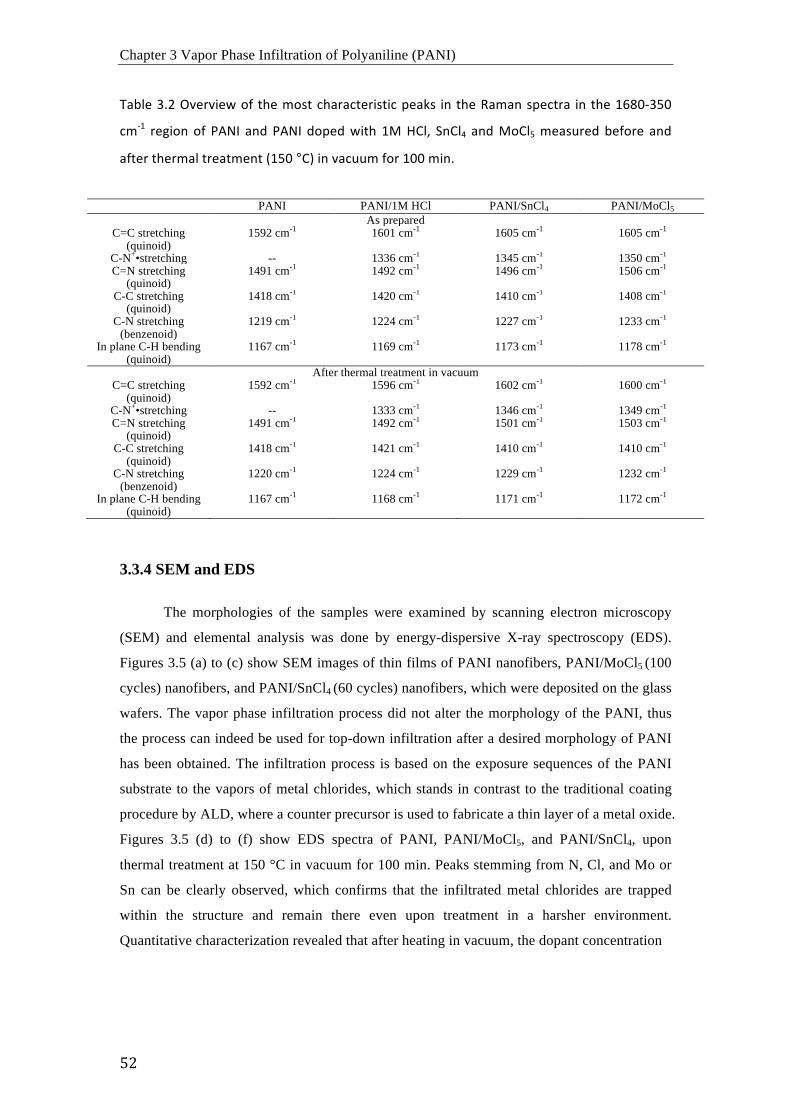
Chapter 3 Vapor Phase Infiltration of Polyaniline (PANI)
52
Table 3.2 Overview of the most characteristic peaks in the Raman spectra in the 1680-‐350
cm-‐1 region of PANI and PANI doped with 1M HCl, SnCl4 and MoCl5 measured before and
after thermal treatment (150 °C) in vacuum for 100 min.
PANI PANI/1M HCl PANI/SnCl4 PANI/MoCl5
As prepared C=C stretching
(quinoid) 1592 cm-1 1601 cm-1 1605 cm-1 1605 cm-1
C-N+•stretching -- 1336 cm-1 1345 cm-1 1350 cm-1 C=N stretching
(quinoid) 1491 cm-1 1492 cm-1 1496 cm-1 1506 cm-1
C-C stretching (quinoid)
1418 cm-1 1420 cm-1 1410 cm-1 1408 cm-1
C-N stretching (benzenoid)
1219 cm-1 1224 cm-1 1227 cm-1 1233 cm-1
In plane C-H bending (quinoid)
1167 cm-1 1169 cm-1 1173 cm-1 1178 cm-1
After thermal treatment in vacuum C=C stretching
(quinoid) 1592 cm-1 1596 cm-1 1602 cm-1 1600 cm-1
C-N+•stretching -- 1333 cm-1 1346 cm-1 1349 cm-1 C=N stretching
(quinoid) 1491 cm-1 1492 cm-1 1501 cm-1 1503 cm-1
C-C stretching (quinoid)
1418 cm-1 1421 cm-1 1410 cm-1 1410 cm-1
C-N stretching (benzenoid)
1220 cm-1 1224 cm-1 1229 cm-1 1232 cm-1
In plane C-H bending (quinoid)
1167 cm-1 1168 cm-1 1171 cm-1 1172 cm-1
3.3.4 SEM and EDS
The morphologies of the samples were examined by scanning electron microscopy
(SEM) and elemental analysis was done by energy-dispersive X-ray spectroscopy (EDS).
Figures 3.5 (a) to (c) show SEM images of thin films of PANI nanofibers, PANI/MoCl5 (100
cycles) nanofibers, and PANI/SnCl4 (60 cycles) nanofibers, which were deposited on the glass
wafers. The vapor phase infiltration process did not alter the morphology of the PANI, thus
the process can indeed be used for top-down infiltration after a desired morphology of PANI
has been obtained. The infiltration process is based on the exposure sequences of the PANI
substrate to the vapors of metal chlorides, which stands in contrast to the traditional coating
procedure by ALD, where a counter precursor is used to fabricate a thin layer of a metal oxide.
Figures 3.5 (d) to (f) show EDS spectra of PANI, PANI/MoCl5, and PANI/SnCl4, upon
thermal treatment at 150 °C in vacuum for 100 min. Peaks stemming from N, Cl, and Mo or
Sn can be clearly observed, which confirms that the infiltrated metal chlorides are trapped
within the structure and remain there even upon treatment in a harsher environment.
Quantitative characterization revealed that after heating in vacuum, the dopant concentration
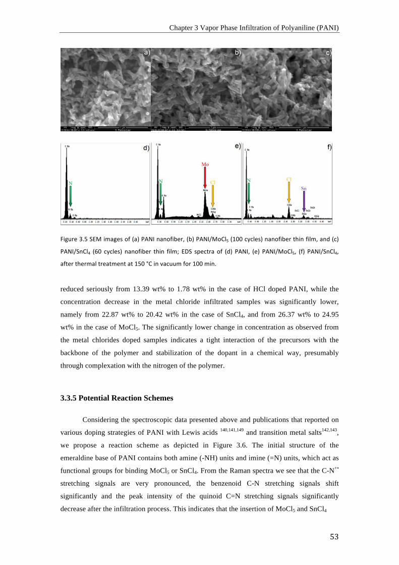
Chapter 3 Vapor Phase Infiltration of Polyaniline (PANI)
53
Figure 3.5 SEM images of (a) PANI nanofiber, (b) PANI/MoCl5 (100 cycles) nanofiber thin film, and (c)
PANI/SnCl4 (60 cycles) nanofiber thin film; EDS spectra of (d) PANI, (e) PANI/MoCl5, (f) PANI/SnCl4,
after thermal treatment at 150 °C in vacuum for 100 min.
reduced seriously from 13.39 wt% to 1.78 wt% in the case of HCl doped PANI, while the
concentration decrease in the metal chloride infiltrated samples was significantly lower,
namely from 22.87 wt% to 20.42 wt% in the case of SnCl4, and from 26.37 wt% to 24.95
wt% in the case of MoCl5. The significantly lower change in concentration as observed from
the metal chlorides doped samples indicates a tight interaction of the precursors with the
backbone of the polymer and stabilization of the dopant in a chemical way, presumably
through complexation with the nitrogen of the polymer.
3.3.5 Potential Reaction Schemes
Considering the spectroscopic data presented above and publications that reported on
various doping strategies of PANI with Lewis acids 140,141,149 and transition metal salts142,143,
we propose a reaction scheme as depicted in Figure 3.6. The initial structure of the
emeraldine base of PANI contains both amine (-NH) units and imine (=N) units, which act as
functional groups for binding MoCl5 or SnCl4. From the Raman spectra we see that the C-N+•
stretching signals are very pronounced, the benzenoid C-N stretching signals shift
significantly and the peak intensity of the quinoid C=N stretching signals significantly
decrease after the infiltration process. This indicates that the insertion of MoCl5 and SnCl4
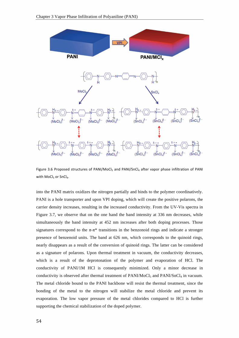
Chapter 3 Vapor Phase Infiltration of Polyaniline (PANI)
-,!
L<M"#,'QH@!/#8B8&,+'&G#";G"#,&'8O'/01(248!69'%=+'/01(2>=!6?'%OG,#'$%B8#'B[%&,' <=O<6G#%G<8='8O'/01('
\<G['48!69'8#'>=!6?H'
into the PANI matrix oxidizes the nitrogen partially and binds to the polymer coordinatively.
PANI is a hole transporter and upon VPI doping, which will create the positive polarons, the
carrier density increases, resulting in the increased conductivity. From the UV-Vis spectra in
Figure 3.7, we observe that on the one hand the band intensity at 336 nm decreases, while
simultaneously the band intensity at 452 nm increases after both doping processes. Those
signatures correspond to the %-%* transitions in the benzonoid rings and indicate a stronger
presence of benzenoid units. The band at 626 nm, which corresponds to the quinoid rings,
nearly disappears as a result of the conversion of quinoid rings. The latter can be considered
as a signature of polarons. Upon thermal treatment in vacuum, the conductivity decreases,
which is a result of the deprotonation of the polymer and evaporation of HCl. The
conductivity of PANI/1M HCl is consequently minimized. Only a minor decrease in
conductivity is observed after thermal treatment of PANI/MoCl5 and PANI/SnCl4 in vacuum.
The metal chloride bound to the PANI backbone will resist the thermal treatment, since the
bonding of the metal to the nitrogen will stabilize the metal chloride and prevent its
evaporation. The low vapor pressure of the metal chlorides compared to HCl is further
supporting the chemical stabilization of the doped polymer.
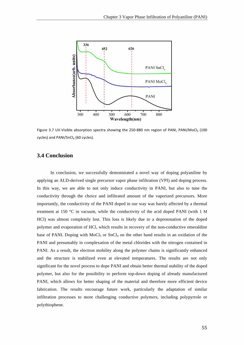
Chapter 3 Vapor Phase Infiltration of Polyaniline (PANI)
55
Figure 3.7 UV-‐Visible absorption spectra showing the 250-‐880 nm region of PANI, PANI/MoCl5 (100
cycles) and PANI/SnCl4 (60 cycles).
3.4 Conclusion
In conclusion, we successfully demonstrated a novel way of doping polyaniline by
applying an ALD-derived single precursor vapor phase infiltration (VPI) and doping process.
In this way, we are able to not only induce conductivity in PANI, but also to tune the
conductivity through the choice and infiltrated amount of the vaporized precursors. More
importantly, the conductivity of the PANI doped in our way was barely affected by a thermal
treatment at 150 °C in vacuum, while the conductivity of the acid doped PANI (with 1 M
HCl) was almost completely lost. This loss is likely due to a deprotonation of the doped
polymer and evaporation of HCl, which results in recovery of the non-conductive emeraldine
base of PANI. Doping with MoCl5 or SnCl4 on the other hand results in an oxidation of the
PANI and presumably in complexation of the metal chlorides with the nitrogen contained in
PANI. As a result, the electron mobility along the polymer chains is significantly enhanced
and the structure is stabilized even at elevated temperatures. The results are not only
significant for the novel process to dope PANI and obtain better thermal stability of the doped
polymer, but also for the possibility to perform top-down doping of already manufactured
PANI, which allows for better shaping of the material and therefore more efficient device
fabrication. The results encourage future work, particularly the adaptation of similar
infiltration processes to more challenging conductive polymers, including polypyrrole or
polythiophene.

Chapter 3 Vapor Phase Infiltration of Polyaniline (PANI)
56
57
Chapter 4
Controlling the Conductivity of Poly(3-hexyl)thiophe-
ne (P3HT) by Low Temperature VPI Process Efficient doping of organic semiconductors is an important prerequisite for the
fabrication of high performance organic electronic devices. In this chapter, a novel single
precursor low-temperature (70 °C) vapor phase infiltration (VPI) process to dope poly(3-
hexyl)thiophene (P3HT) is described. The infiltration is performed with the metal containing
atomic layer deposition (ALD) precursor MoCl5. The conductivities of the polymer were
assessed with four-point probe measurements and showed significant enhancement of up to 5
orders of magnitude, confirming the efficiency of the VPI process. The chemical changes
resulting from the infiltration of P3HT were characterized applying UV-Vis, Raman, XPS,
and FTIR spectroscopy. The crystalline state of the material was analyzed by XRD. SEM
micrographs and AFM images show that the morphologies of the samples before and after
MoCl5 infiltration process did not seriously change. TEM images of cross-sections of the thin
film clearly show that the vapor phase infiltration process results in the incorporation of Mo
into the bulk of the polymer.
This chapter describes the part of the thesis that was published in the journal Journal
of Materials Chemistry C from the Royal Society of Chemistry (RSC). Graphs, figures and
parts of the text of the publication are reused in this thesis with permission of the publisher.
Article:
Efficient and Controllable Vapor to Solid Doping of the Polythiophene P3HT by Low
Temperature Vapor Phase Infiltration. Weike Wang, Chaoqiu Chen, Christopher Tollan, Fan
Yang, Yong Qin, and Mato Knez. Journal of Materials Chemistry C. 2017, 5, 2686-2694.
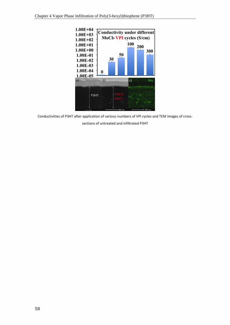
Chapter 4 Vapor Phase Infiltration of Poly(3-hexyl)thiophene (P3HT)
58
Conductivities of P3HT after application of various numbers of VPI cycles and TEM images of cross-‐
sections of untreated and infiltrated P3HT
Chapter 4 Vapor Phase Infiltration of Poly(3-hexyl)thiophene (P3HT)
59
4.1 Introduction
Over the past years, organic semiconductors (OSCs) have been extensively
investigated due to their tremendous importance as integral part of a wide range of electrical
devices150-153. For instance, previous studies have reported on enhanced mobilities of charge
carriers in field-effect transistors (FETs) achieved by trap filling154, improved charge injection
in light-emitting diodes (LEDs)155,156 and, more recently, superior power conversion
efficiencies in organic photovoltaics157-162. The development of inorganic semiconductor
devices has revealed that crucially important steps for enabling engineering of efficient
electronics include controllable doping and realization of stable and controllable doped
transport layers for both p - and n - type materials. The same considerations apply for the
organic counterpart as well. However, doping strategies for OSCs are typically dissimilar to
those for their inorganic counterparts and thus optimal schemes need to be evaluated from
scratch. Even though doped OSC thin films have been shown to exhibit conductivities to 5-8
orders of magnitude higher than undoped films163-164, better understanding of the chemistry
that occurs upon doping and evaluation of various strategies for improving their efficiency is
expected to result in even more efficient OSCs, which will strongly impact the emerging field
of organic electronics.
Doping of inorganic semiconductors is meanwhile well developed. Controlled
introduction of atomic or ionic impurities into semiconductors became the fundamental
enabler for the functionality of modern electronic devices as we experience them
nowadays165. The doping process allows tuning the band alignment at interfaces and markedly
increases the conductivity even at ultralow doping ratios, as typically every covalently bound
dopant atom donates one mobile charge carrier to the highly crystalline and ultra-pure
semiconductor matrix. In contrast, doping of OSCs is achieved by adding comparatively
strong electron acceptors or donors, resulting in a significant increase of the charge carrier
density and therefore conductivity of such materials. Stable p-type doping is nowadays
typically achieved by introducing transition metal oxides such as MoO3166 or WO3
167 into the
polymer or by adding molecular π-electron acceptors, for example, tetracyano-2,3,5,6-
tetrafluoroquinodimethane (F4TCNQ)168-170, 2,2′-(perfluoronaphthalene-2,6-diylidene)
dimalononitrile (F6TCNNQ)171, or 1,4,5,8,9,11-
hexaazatriphenylenehexacarbonitrile(HATCN)172. The principle of doping with molecular π-
electron acceptors has been proven to be applicable to a wide range of molecular
semiconductors and polymers. The resulting conductivity of such F4TCNQ-doped organic
materials can exceed 1 S/cm at highest dopant concentrations173. Among the various
molecular dopants, F4TCNQ gained prominence as reference dopant. The fundamental
Chapter 4 Vapor Phase Infiltration of Poly(3-hexyl)thiophene (P3HT)
60
mechanisms that determine the concentration and mobility of mobile holes in F4TCNQ-
doped samples of the polymer poly(3-hexyl)thiophene, P3HT, have been identified and
showed that in this particular donor-acceptor couple almost all employed F4TCNQ molecules
undergo integer charge transfer (ICT), meaning that an electron is fully transferred from the
π-electron system of a P3HT site to the F4TCNQ acceptor. This eventually results in
positively charged P3HT (P3HT+) and negtively charged F4TCNQ (F4TCNQ-)174. Thus,
F4TCNQ-doping leads to a strong increase in the density of mobile charge carriers and
consequently the electrical conductivity. However, as an alternative to the common π-electron
acceptors, some recent reports introduced the possibility of doping of polymers with Lewis
acids. The Bazan and Neher groups have studied the optical and charge carrier transport
properties of various polymers which were doped by the strong Lewis acid
tris(pentafluorophenyl)-borane (BCF)174-178. The effect has been explained with a formation of
Lewis acid-base adducts. In the case of p-type doping with BFC, the electrophilic borane
center binds to a moiety carrying an accessible lone pair of electrons, for example, the
nitrogen atoms present in pyridine or the benzothiadiazole units of the semiconductor. The
binding induces a redistribution of the electron density, that is, a charge transfer between the
semiconductor and dopant occurs. This will eventually change the oxidation state of each of
the partners, liberating charge carriers that become available for electrical conduction.
Given the already published results, the mentioned doping with Lewis acid appears
to be a promising approach for obtaining efficient OSCs, but the doping process itself may
still be further improved. Here, we apply a novel procedure for doping P3HT with the Lewis
acid molybdenum (V) chloride (MoCl5) and a detailed analysis of the resulting doped
polymer. Doping of polymers is typically performed in liquid state, which introduces various
chemical species such as solvents or byproducts of chemical reactions into the substrate with
all the related potentially negative consequences for the conductivity and/or stability of the
resulting material. Besides, the possibility of shaping the polymer after doping process is
often hampered because of dopant-induced crystallization or hardening of the polymer. For
avoiding such negative influences, we apply an alternative approach, vapor phase infiltration
(VPI) process, for injecting the Lewis acid into the polymeric substrate. The VPI process is
derived from atomic layer deposition (ALD)76, and applies the same processing technology,
that is, exposure of the substrates to vaporized chemicals in a pulsed manner with stringent
control of the dosing parameters. This procedure allows taking advantage of the mobility of a
vaporized chemical and its ability to diffuse into and react with polymeric substrates88.
Incorporation of inorganic materials into polymers often enhances some physical properties
of the resulting composite or hybrid material110-114. For example, our earlier works
demonstrated that infiltration of metal oxides or metal ions into various (bio)polymers,
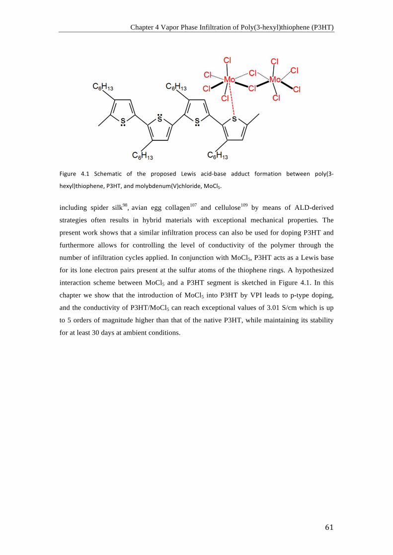
Chapter 4 Vapor Phase Infiltration of Poly(3-hexyl)thiophene (P3HT)
61
Figure 4.1 Schematic of the proposed Lewis acid-‐base adduct formation between poly(3-‐
hexyl)thiophene, P3HT, and molybdenum(V)chloride, MoCl5.
including spider silk98, avian egg collagen107 and cellulose109 by means of ALD-derived
strategies often results in hybrid materials with exceptional mechanical properties. The
present work shows that a similar infiltration process can also be used for doping P3HT and
furthermore allows for controlling the level of conductivity of the polymer through the
number of infiltration cycles applied. In conjunction with MoCl5, P3HT acts as a Lewis base
for its lone electron pairs present at the sulfur atoms of the thiophene rings. A hypothesized
interaction scheme between MoCl5 and a P3HT segment is sketched in Figure 4.1. In this
chapter we show that the introduction of MoCl5 into P3HT by VPI leads to p-type doping,
and the conductivity of P3HT/MoCl5 can reach exceptional values of 3.01 S/cm which is up
to 5 orders of magnitude higher than that of the native P3HT, while maintaining its stability
for at least 30 days at ambient conditions.
Chapter 4 Vapor Phase Infiltration of Poly(3-hexyl)thiophene (P3HT)
62
4.2 Experimental Section
4.2.1 Preparation the Poly (3-hexyl) thiophene (P3HT) Thin Film
1,2-Dichlorobenzene (DCB) was purchased from Aldrich and used as received.
Poly(3-hexylthiophene-2,5-diyl) (P3HT, Mw = 50 000 g mol-1, 95% regioregularity) was
purchased from Reike Metals, Inc. U.S.A and used as-received. As substrates, the electrically
insulating glass slides were used, which were cleaned thoroughly by sonication in acetone,
methanol and isopropanol for 1 h prior to coating with P3HT. For pristine films, 37 mg P3HT
was dissolved in 1 mL DCB. The thin films (≈ 35 µm) were prepared via drop casting the
solution on glass substrates (1.3 cm×1.3 cm) at ambient conditions. All samples were soft-
baked at 70 °C overnight to remove excess solvent.
4.2.2 Vapor Phase Infiltration Process of P3HT Thin Film
Vapor-phase infiltration was performed using a homemade atomic layer deposition
tool. Pristine P3HT films coated on glass substrates were exposed to vapors of MoCl5 in a
pulse-exposure-purge sequence with various numbers of repetition cycles. One cycle of the
process consisted of following settings: the precursor (MoCl5, 95%, Aldrich) was pulsed into
the reaction chamber for 5 s and thereafter exposure of the substrates to the vapors in the
reaction chamber was allowed for 120 s. The exposure was followed by a 60 s purge step.
The cycle was repeated with the number of cycles varying between 10 and 300. As carrier
and purging gas N2 (99.99%) was used. The chamber temperature was kept constant at 70 °C
during the infiltration process with the base pressure of the reactor having been maintained at
50 mTorr. Since at room temperature MoCl5 is solid, heating of the precursor to 85 °C was
required to obtain a reasonable vapor pressure.
4.2.3 Characterization
Absorption spectra of the samples were recorded between 360-890 nm using a UV-
Vis spectrophotometer (V-630 BIO, JASCO).
Raman spectra with a 532 nm (100 × objective) exciting wavelength were collected
with a Raman microscope (Alpha 300S, WITec). The laser power was kept at 0.02 mW and
the acquisition time was limited to 10-20 s for each measurement to avoid sample degradation.
The Raman spectra were background corrected and obtained by averaging spectra obtained
from five different regions of each sample.
Chapter 4 Vapor Phase Infiltration of Poly(3-hexyl)thiophene (P3HT)
63
XPS experiments were conducted using a PHOIBOS photoelectron spectrometer
equipped with an Al Kα X-ray source (12 mA, 8.33 kV) as the incident photon radiation, and
the spectra were standardized using the C1s peak at 284.6 eV.
X-ray diffraction (XRD) analysis was carried with a powder diffractometer (X´pert
with 45 kV, 40 mA; PANalytical) with Ni-filtered Cu Kα radiation.
Infrared spectra of the samples were recorded between 760 and 1610 cm-1 with a FTIR
Spectrometer (Frontier; PerkinElmer).
The morphology of the samples was characterized by scanning electron microscopy
(SEM, Quanta 250 FEG; FEI) and the chemical composition was analyzed with energy-
dispersive X-ray spectroscopy (EDS). Thickness measurements were carried out on a cleaved
cross-section of the sample by FEG-SEM.
AFM analysis was performed on P3HT-coated glass slides, employing a 5500 AFM
(Keysight, Santa Clara). The AFM probe was a HQ-NSC 14/Al BS tip with an approximate
tip radius of 8 nm. The spring constant of the cantilevers was 5 N/m and a resonance
frequency of 160 KHz was used in tapping mode; data processing was done using the
software Gwyddion.
TEM images were recorded and EDS analysis were carried out with an FEI Titan
microscope using an acceleration voltage of 300 kV in scanning transimission electron
microscopy mode and an EDAX SDD detector. The focused ion beam (FIB) used for
lamellae preparation was a dual beam Helios Nanolab 450S from FEI. The FIB lamellae were
prepared from a glass wafer with the P3HT thin film deposited on it and after the entire wafer
had undergone MoCl5 vapor phase infiltration treatment. The block was extracted by
standard methods using a Pt electron beam deposition to initially protect the sample surface
before any ion beam deposition was carried out. The block was thinned to transparency on a
copper "Omniprobe" grid using a 5 kV gallium ion beam at 8 pA for final surface preparation.
The conductivities of the thin films were measured applying a four-point probe
technique with a source measurement unit (Keithley 2611). For each VPI experiment four or
five individual samples were tested for each VPI process cycle number. The resulting
conductivity, σ, was calculated according to the formula,
)( VI d/2ln πσ =
where I is the current, V is the voltage and d is the whole polymer film thickness.
Chapter 4 Vapor Phase Infiltration of Poly(3-hexyl)thiophene (P3HT)
64
4.3 Results and Discussion
4.3.1 Assessment of the electrical conductivity
The functionalization of P3HT thin films with MoCl5 through the vapor phase
infiltration process resulted in the introduction of mobile carriers into the conjugated polymer,
and therefore in an enhanced conductivity. In contrast to a typical ALD process or previously
described ALD-based infiltration strategies, where a substrate is sequentially exposed to
vapors of two precursors, here we expose the substrate to the vapor of only one precursor and
allow sufficient time for the precursor to diffuse into subsurface areas of the substrate. After
infiltration, we measured the electrical characteristics of the samples. Figure 4.2 (a) shows the
room temperature I-V plots of the various fabricated P3HT samples in comparison to the
untreated polymer. The thicknesses of all samples were comparable (≈ 35 µm). The plots of
P3HT/MoCl5 are linear, confirming ohmic behavior over the whole measurement range.
Untreated P3HT thin films act as reference with conductivity values of 1.44×10⁻⁵ S/cm. The
increase in conductivity confirms the possibility of using the vaporized Lewis acid MoCl5 for
doping P3HT. The values for the electrical conductivities of the samples were extracted from
the slopes of the I-V plots. An important observation resulting from the measurements is that
the conductivity of the doped P3HT films stands in non-linear correlation with the number of
infiltration cycles as can be seen in Figure 4.2 (b). The peak value of the conductivity with
3.01 S/cm is reached after 100 infiltration cycles, while lower and higher number of cycles
result in lower conductivities.
At low MoCl5 doping levels, the carrier concentration will increase linearly with the
doping concentration while their mobility will decrease unproportionally, hence the
conductivity will increase with doping. However, upon heavy doping, a significant fraction of
the dopant remains inactive. Once the concentration of dopants exceeds the solubility limit in
the polymer, the dopants will cluster resulting in the carrier concentration stagnating. These
dopants will further cause enhanced scattering of the electrons and contribute to a decrease in
their mobility.
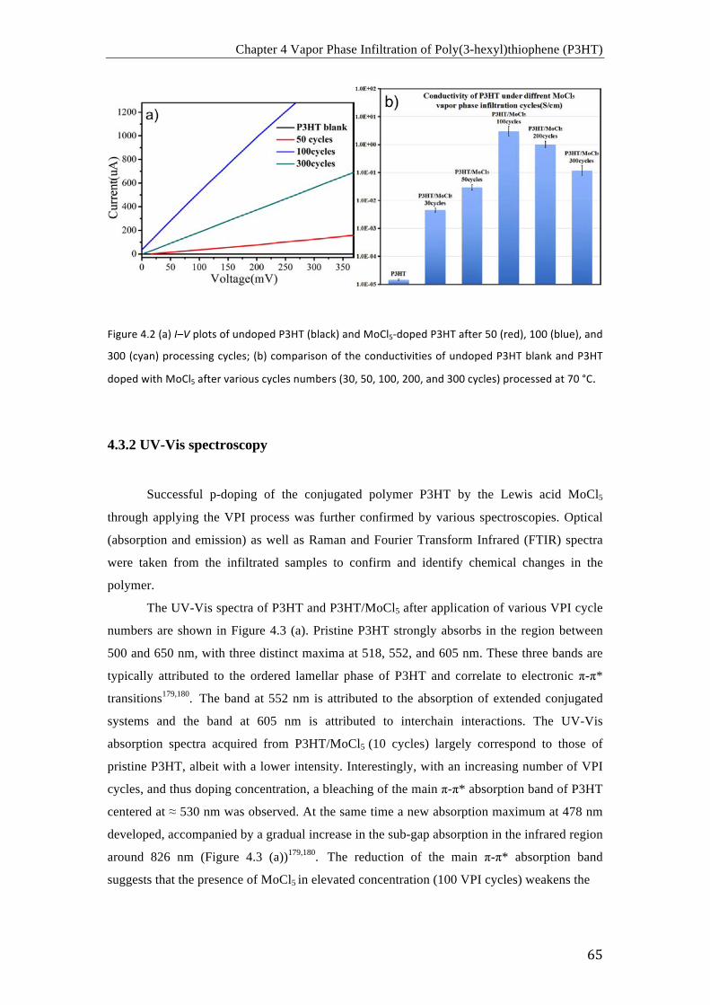
Chapter 4 Vapor Phase Infiltration of Poly(3-hexyl)thiophene (P3HT)
65
Figure 4.2 (a) I–V plots of undoped P3HT (black) and MoCl5-‐doped P3HT after 50 (red), 100 (blue), and
300 (cyan) processing cycles; (b) comparison of the conductivities of undoped P3HT blank and P3HT
doped with MoCl5 after various cycles numbers (30, 50, 100, 200, and 300 cycles) processed at 70 °C.
4.3.2 UV-Vis spectroscopy
Successful p-doping of the conjugated polymer P3HT by the Lewis acid MoCl5
through applying the VPI process was further confirmed by various spectroscopies. Optical
(absorption and emission) as well as Raman and Fourier Transform Infrared (FTIR) spectra
were taken from the infiltrated samples to confirm and identify chemical changes in the
polymer.
The UV-Vis spectra of P3HT and P3HT/MoCl5 after application of various VPI cycle
numbers are shown in Figure 4.3 (a). Pristine P3HT strongly absorbs in the region between
500 and 650 nm, with three distinct maxima at 518, 552, and 605 nm. These three bands are
typically attributed to the ordered lamellar phase of P3HT and correlate to electronic π-π*
transitions179,180. The band at 552 nm is attributed to the absorption of extended conjugated
systems and the band at 605 nm is attributed to interchain interactions. The UV-Vis
absorption spectra acquired from P3HT/MoCl5 (10 cycles) largely correspond to those of
pristine P3HT, albeit with a lower intensity. Interestingly, with an increasing number of VPI
cycles, and thus doping concentration, a bleaching of the main π-π* absorption band of P3HT
centered at ≈ 530 nm was observed. At the same time a new absorption maximum at 478 nm
developed, accompanied by a gradual increase in the sub-gap absorption in the infrared region
around 826 nm (Figure 4.3 (a))179,180. The reduction of the main π-π* absorption band
suggests that the presence of MoCl5 in elevated concentration (100 VPI cycles) weakens the
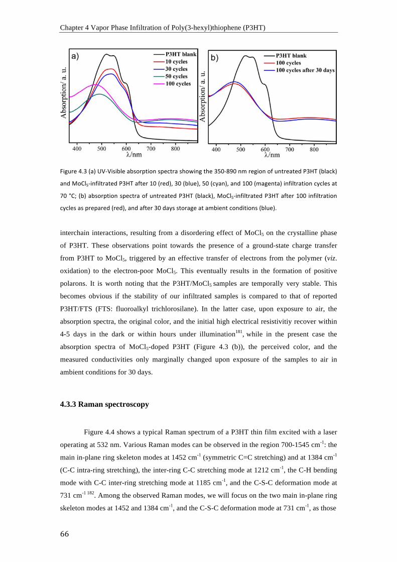
Chapter 4 Vapor Phase Infiltration of Poly(3-hexyl)thiophene (P3HT)
66
Figure 4.3 (a) UV-‐Visible absorption spectra showing the 350-‐890 nm region of untreated P3HT (black)
and MoCl5-‐infiltrated P3HT after 10 (red), 30 (blue), 50 (cyan), and 100 (magenta) infiltration cycles at
70 °C; (b) absorption spectra of untreated P3HT (black), MoCl5-‐infiltrated P3HT after 100 infiltration
cycles as prepared (red), and after 30 days storage at ambient conditions (blue).
interchain interactions, resulting from a disordering effect of MoCl5 on the crystalline phase
of P3HT. These observations point towards the presence of a ground-state charge transfer
from P3HT to MoCl5, triggered by an effective transfer of electrons from the polymer (viz.
oxidation) to the electron-poor MoCl5. This eventually results in the formation of positive
polarons. It is worth noting that the P3HT/MoCl5 samples are temporally very stable. This
becomes obvious if the stability of our infiltrated samples is compared to that of reported
P3HT/FTS (FTS: fluoroalkyl trichlorosilane). In the latter case, upon exposure to air, the
absorption spectra, the original color, and the initial high electrical resistivitiy recover within
4-5 days in the dark or within hours under illumination181, while in the present case the
absorption spectra of MoCl5-doped P3HT (Figure 4.3 (b)), the perceived color, and the
measured conductivities only marginally changed upon exposure of the samples to air in
ambient conditions for 30 days.
4.3.3 Raman spectroscopy
Figure 4.4 shows a typical Raman spectrum of a P3HT thin film excited with a laser
operating at 532 nm. Various Raman modes can be observed in the region 700-1545 cm-1: the
main in-plane ring skeleton modes at 1452 cm-1 (symmetric C=C stretching) and at 1384 cm-1
(C-C intra-ring stretching), the inter-ring C-C stretching mode at 1212 cm-1, the C-H bending
mode with C-C inter-ring stretching mode at 1185 cm-1, and the C-S-C deformation mode at
731 cm-1 182. Among the observed Raman modes, we will focus on the two main in-plane ring
skeleton modes at 1452 and 1384 cm-1, and the C-S-C deformation mode at 731 cm-1, as those
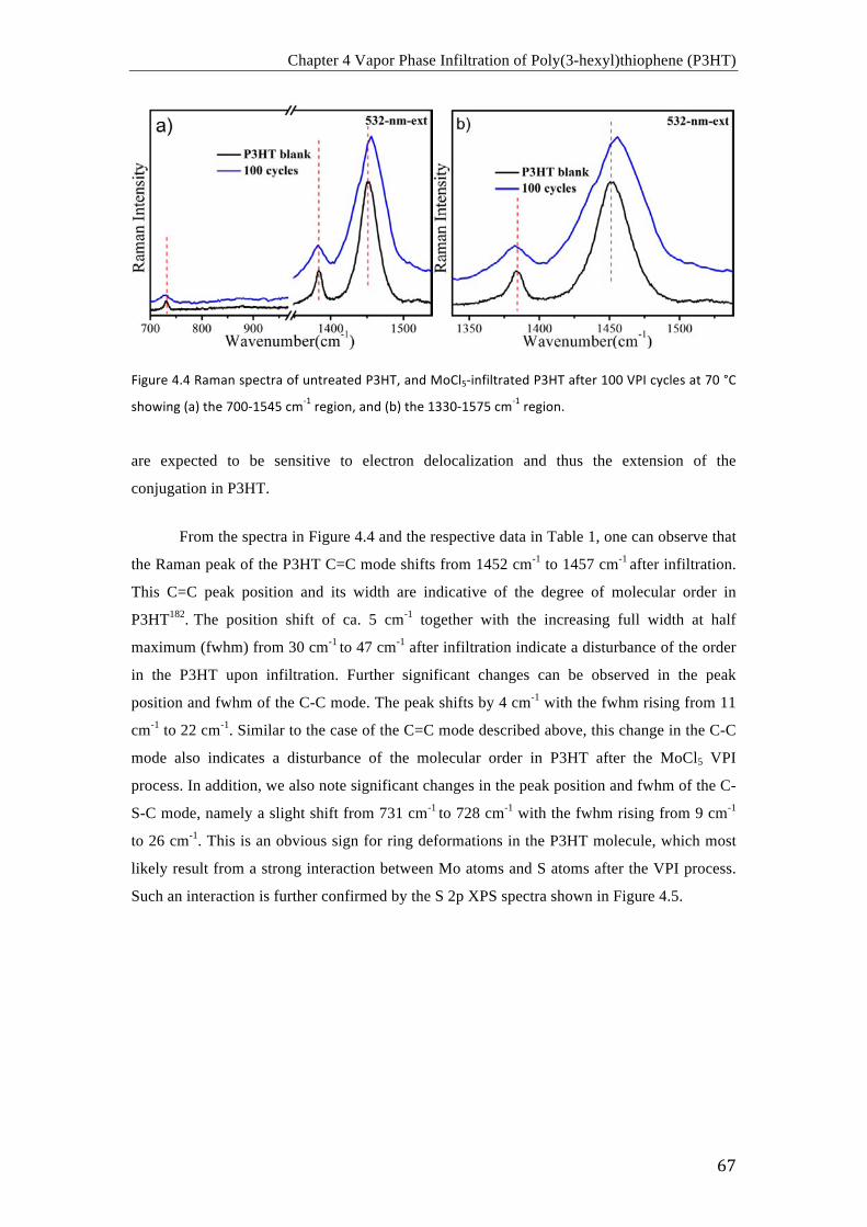
Chapter 4 Vapor Phase Infiltration of Poly(3-hexyl)thiophene (P3HT)
67
Figure 4.4 Raman spectra of untreated P3HT, and MoCl5-‐infiltrated P3HT after 100 VPI cycles at 70 °C
showing (a) the 700-‐1545 cm-‐1 region, and (b) the 1330-‐1575 cm-‐1 region.
are expected to be sensitive to electron delocalization and thus the extension of the
conjugation in P3HT.
From the spectra in Figure 4.4 and the respective data in Table 1, one can observe that
the Raman peak of the P3HT C=C mode shifts from 1452 cm-1 to 1457 cm-1 after infiltration.
This C=C peak position and its width are indicative of the degree of molecular order in
P3HT182. The position shift of ca. 5 cm-1 together with the increasing full width at half
maximum (fwhm) from 30 cm-1 to 47 cm-1 after infiltration indicate a disturbance of the order
in the P3HT upon infiltration. Further significant changes can be observed in the peak
position and fwhm of the C-C mode. The peak shifts by 4 cm-1 with the fwhm rising from 11
cm-1 to 22 cm-1. Similar to the case of the C=C mode described above, this change in the C-C
mode also indicates a disturbance of the molecular order in P3HT after the MoCl5 VPI
process. In addition, we also note significant changes in the peak position and fwhm of the C-
S-C mode, namely a slight shift from 731 cm-1 to 728 cm-1 with the fwhm rising from 9 cm-1
to 26 cm-1. This is an obvious sign for ring deformations in the P3HT molecule, which most
likely result from a strong interaction between Mo atoms and S atoms after the VPI process.
Such an interaction is further confirmed by the S 2p XPS spectra shown in Figure 4.5.
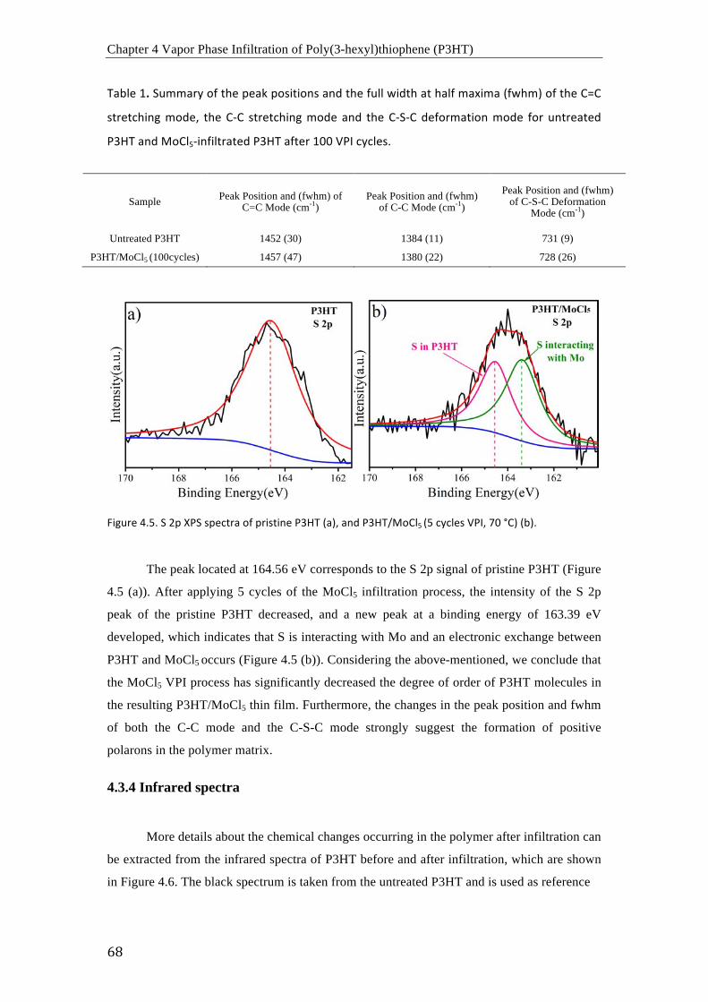
Chapter 4 Vapor Phase Infiltration of Poly(3-hexyl)thiophene (P3HT)
68
Table 1. Summary of the peak positions and the full width at half maxima (fwhm) of the C=C
stretching mode, the C-‐C stretching mode and the C-‐S-‐C deformation mode for untreated
P3HT and MoCl5-‐infiltrated P3HT after 100 VPI cycles.
Sample Peak Position and (fwhm) of C=C Mode (cm-1)
Peak Position and (fwhm) of C-C Mode (cm-1)
Peak Position and (fwhm) of C-S-C Deformation
Mode (cm-1)
Untreated P3HT 1452 (30) 1384 (11) 731 (9)
P3HT/MoCl5 (100cycles) 1457 (47) 1380 (22) 728 (26)
Figure 4.5. S 2p XPS spectra of pristine P3HT (a), and P3HT/MoCl5 (5 cycles VPI, 70 °C) (b).
The peak located at 164.56 eV corresponds to the S 2p signal of pristine P3HT (Figure
4.5 (a)). After applying 5 cycles of the MoCl5 infiltration process, the intensity of the S 2p
peak of the pristine P3HT decreased, and a new peak at a binding energy of 163.39 eV
developed, which indicates that S is interacting with Mo and an electronic exchange between
P3HT and MoCl5 occurs (Figure 4.5 (b)). Considering the above-mentioned, we conclude that
the MoCl5 VPI process has significantly decreased the degree of order of P3HT molecules in
the resulting P3HT/MoCl5 thin film. Furthermore, the changes in the peak position and fwhm
of both the C-C mode and the C-S-C mode strongly suggest the formation of positive
polarons in the polymer matrix.
4.3.4 Infrared spectra
More details about the chemical changes occurring in the polymer after infiltration can
be extracted from the infrared spectra of P3HT before and after infiltration, which are shown
in Figure 4.6. The black spectrum is taken from the untreated P3HT and is used as reference
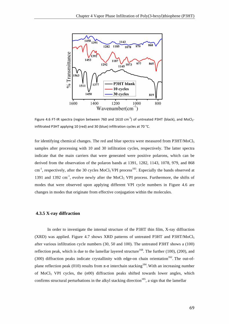
Chapter 4 Vapor Phase Infiltration of Poly(3-hexyl)thiophene (P3HT)
69
Figure 4.6 FT-‐IR spectra (region between 760 and 1610 cm-‐1) of untreated P3HT (black), and MoCl5-‐
infiltrated P3HT applying 10 (red) and 30 (blue) infiltration cycles at 70 °C.
for identifying chemical changes. The red and blue spectra were measured from P3HT/MoCl5
samples after processing with 10 and 30 infiltration cycles, respectively. The latter spectra
indicate that the main carriers that were generated were positive polarons, which can be
derived from the observation of the polaron bands at 1391, 1282, 1143, 1078, 979, and 868
cm-1, respectively, after the 30 cycles MoCl5 VPI process183. Especially the bands observed at
1391 and 1392 cm-1, evolve newly after the MoCl5 VPI process. Furthermore, the shifts of
modes that were observed upon applying different VPI cycle numbers in Figure 4.6 are
changes in modes that originate from effective conjugation within the molecules.
4.3.5 X-ray diffraction
In order to investigate the internal structure of the P3HT thin film, X-ray diffraction
(XRD) was applied. Figure 4.7 shows XRD patterns of untreated P3HT and P3HT/MoCl5
after various infiltration cycle numbers (30, 50 and 100). The untreated P3HT shows a (100)
reflection peak, which is due to the lamellar layered structure168. The further (100), (200), and
(300) diffraction peaks indicate crystallinity with edge-on chain orientation162. The out-of-
plane reflection peak (010) results from π-π interchain stacking184. With an increasing number
of MoCl5 VPI cycles, the (n00) diffraction peaks shifted towards lower angles, which
confirms structural perturbations in the alkyl stacking direction185, a sign that the lamellar
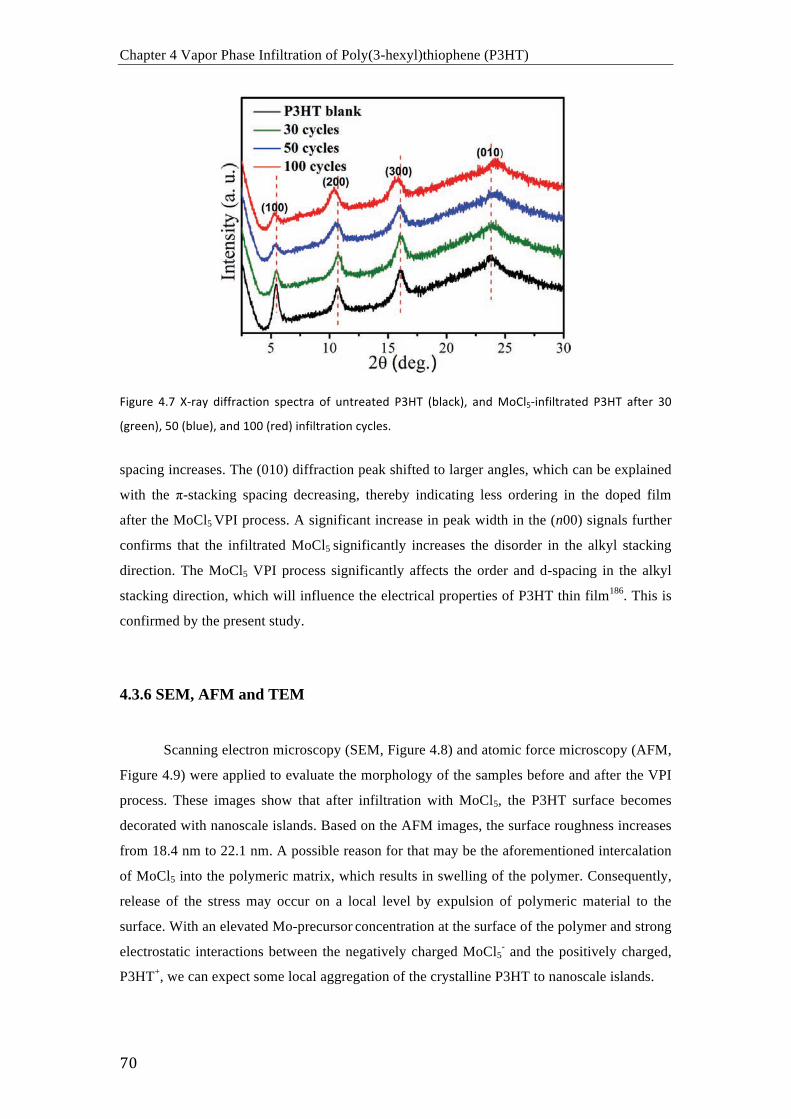
Chapter 4 Vapor Phase Infiltration of Poly(3-hexyl)thiophene (P3HT)
*/!
!
L<M"#,' ?HV' e)#%C' +<OO#%;G<8=' &B,;G#%' 8O' "=G#,%G,+' /Q5R' -D6%;_.7' %=+' 48!69)<=O<6G#%G,+' /Q5R' %OG,#' Q:'
-M#,,=.7'9:'-D6",.7'%=+'3::'-#,+.'<=O<6G#%G<8=';C;6,&H
spacing increases. The (010) diffraction peak shifted to larger angles, which can be explained
with the %-stacking spacing decreasing, thereby indicating less ordering in the doped film
after the MoCl5 VPI process. A significant increase in peak width in the (n00) signals further
confirms that the infiltrated MoCl5 significantly increases the disorder in the alkyl stacking
direction. The MoCl5 VPI process significantly affects the order and d-spacing in the alkyl
stacking direction, which will influence the electrical properties of P3HT thin film186. This is
confirmed by the present study.
4.3.6 SEM, AFM and TEM
Scanning electron microscopy (SEM, Figure 4.8) and atomic force microscopy (AFM,
Figure 4.9) were applied to evaluate the morphology of the samples before and after the VPI
process. These images show that after infiltration with MoCl5, the P3HT surface becomes
decorated with nanoscale islands. Based on the AFM images, the surface roughness increases
from 18.4 nm to 22.1 nm. A possible reason for that may be the aforementioned intercalation
of MoCl5 into the polymeric matrix, which results in swelling of the polymer. Consequently,
release of the stress may occur on a local level by expulsion of polymeric material to the
surface. With an elevated Mo-precursor concentration at the surface of the polymer and strong
electrostatic interactions between the negatively charged MoCl5- and the positively charged,
P3HT+, we can expect some local aggregation of the crystalline P3HT to nanoscale islands.
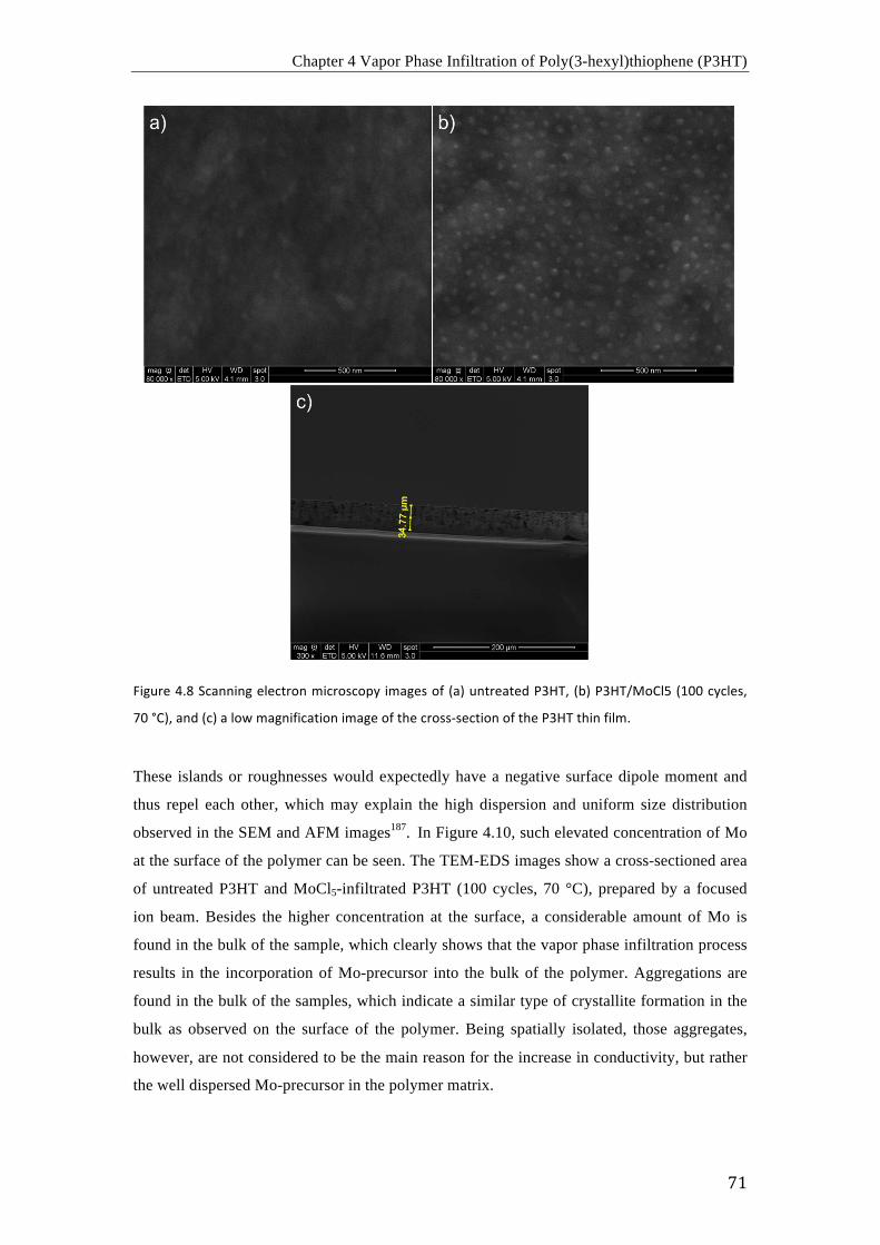
Chapter 4 Vapor Phase Infiltration of Poly(3-hexyl)thiophene (P3HT)
71
Figure 4.8 Scanning electron microscopy images of (a) untreated P3HT, (b) P3HT/MoCl5 (100 cycles,
70 °C), and (c) a low magnification image of the cross-‐section of the P3HT thin film.
These islands or roughnesses would expectedly have a negative surface dipole moment and
thus repel each other, which may explain the high dispersion and uniform size distribution
observed in the SEM and AFM images187. In Figure 4.10, such elevated concentration of Mo
at the surface of the polymer can be seen. The TEM-EDS images show a cross-sectioned area
of untreated P3HT and MoCl5-infiltrated P3HT (100 cycles, 70 °C), prepared by a focused
ion beam. Besides the higher concentration at the surface, a considerable amount of Mo is
found in the bulk of the sample, which clearly shows that the vapor phase infiltration process
results in the incorporation of Mo-precursor into the bulk of the polymer. Aggregations are
found in the bulk of the samples, which indicate a similar type of crystallite formation in the
bulk as observed on the surface of the polymer. Being spatially isolated, those aggregates,
however, are not considered to be the main reason for the increase in conductivity, but rather
the well dispersed Mo-precursor in the polymer matrix.
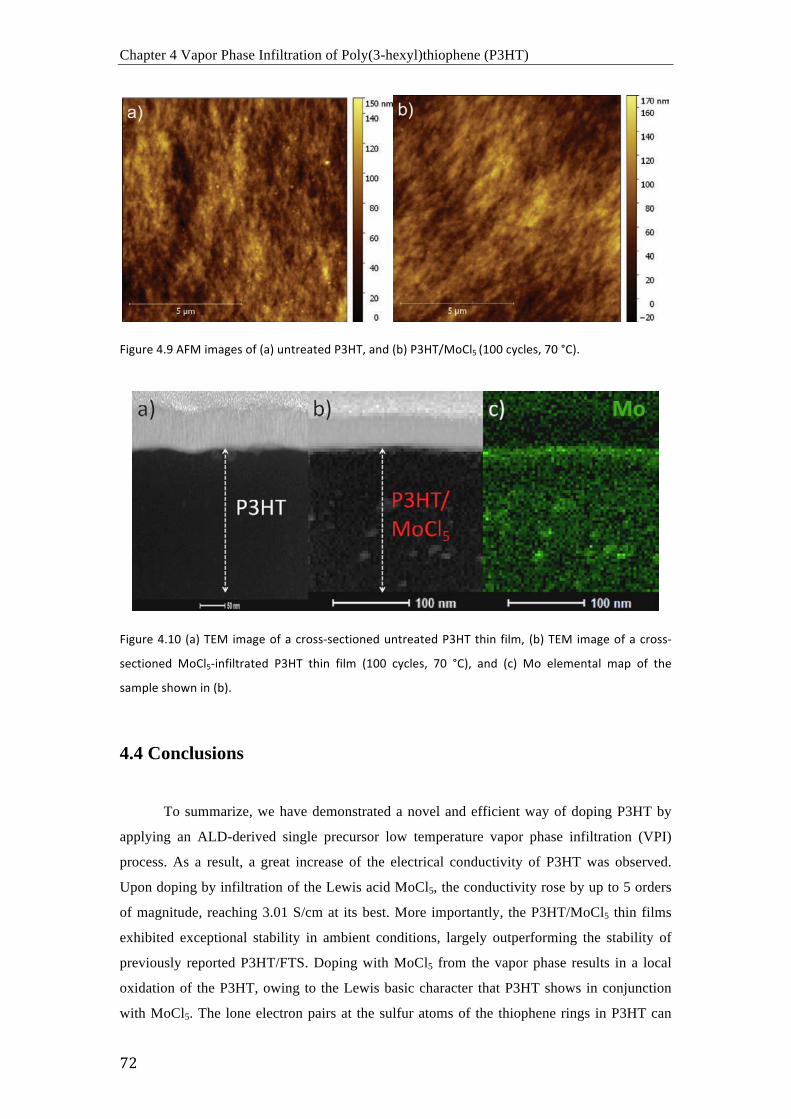
Chapter 4 Vapor Phase Infiltration of Poly(3-hexyl)thiophene (P3HT)
*)!
!
L<M"#,'?Hc'0L4'<E%M,&'8O'-%.'"=G#,%G,+'/Q5R7'%=+'-D.'/Q5R248!69'-3::';C;6,&7'V:'i!.H'
!
L<M"#,'?H3:'-%.'RI4'<E%M,'8O'%';#8&&)&,;G<8=,+'"=G#,%G,+'/Q5R'G[<=' O<6E7' -D.'RI4'<E%M,'8O'%';#8&&)
&,;G<8=,+' 48!69)<=O<6G#%G,+' /Q5R' G[<=' O<6E' -3::' ;C;6,&7' V:' i!.7' %=+' -;.' 48' ,6,E,=G%6' E%B' 8O' G[,'
&%EB6,'&[8\='<='-D.H'
4.4 Conclusions
To summarize, we have demonstrated a novel and efficient way of doping P3HT by
applying an ALD-derived single precursor low temperature vapor phase infiltration (VPI)
process. As a result, a great increase of the electrical conductivity of P3HT was observed.
Upon doping by infiltration of the Lewis acid MoCl5, the conductivity rose by up to 5 orders
of magnitude, reaching 3.01 S/cm at its best. More importantly, the P3HT/MoCl5 thin films
exhibited exceptional stability in ambient conditions, largely outperforming the stability of
previously reported P3HT/FTS. Doping with MoCl5 from the vapor phase results in a local
oxidation of the P3HT, owing to the Lewis basic character that P3HT shows in conjunction
with MoCl5. The lone electron pairs at the sulfur atoms of the thiophene rings in P3HT can
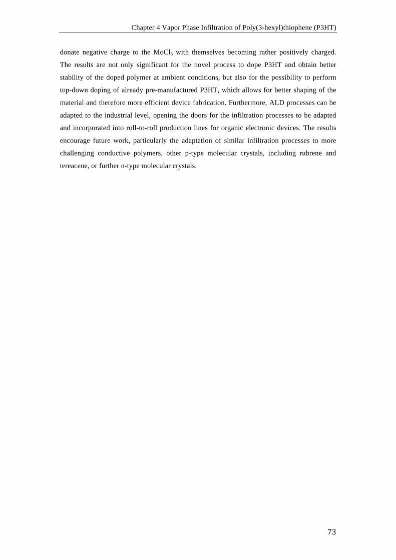
Chapter 4 Vapor Phase Infiltration of Poly(3-hexyl)thiophene (P3HT)
73
donate negative charge to the MoCl5 with themselves becoming rather positively charged.
The results are not only significant for the novel process to dope P3HT and obtain better
stability of the doped polymer at ambient conditions, but also for the possibility to perform
top-down doping of already pre-manufactured P3HT, which allows for better shaping of the
material and therefore more efficient device fabrication. Furthermore, ALD processes can be
adapted to the industrial level, opening the doors for the infiltration processes to be adapted
and incorporated into roll-to-roll production lines for organic electronic devices. The results
encourage future work, particularly the adaptation of similar infiltration processes to more
challenging conductive polymers, other p-type molecular crystals, including rubrene and
tereacene, or further n-type molecular crystals.

Chapter 4 Vapor Phase Infiltration of Poly(3-hexyl)thiophene (P3HT)
74
75
Chapter 5
Conductive Polymer-Inorganic Hybrid Materials
through Synergistic Mutual Doping of the
Constituents Polymer matrix based inorganic-organic hybrid materials are at the cutting edge of
current research for their great promise of merging properties of soft and hard solids in one
material. Infiltration of polymers with vapors of reactive metal organics is a pathway for post-
synthetic blending of the polymer with inorganic materials. This chapter shows that the MPI
process is also an excellent method for fabricating conductive hybrid materials. Polyaniline
(PANI) was infiltrated with the precursor pair diethylzinc (DEZ) and H2O and the initially
insulating polymer was converted to a PANI/ZnO hybrid with conductivities as high as 18.42
S/cm. The conductivity is based on a synergistic effect of the constituting materials where the
inorganic and the polymeric fractions mutually act as dopants for the counterpart. The process
temperature is a very important factor for a successful infiltration and the number of applied
infiltration cycles allows tuning the level of conductivity of the resulting PANI/ZnO.
This chapter describes the part of the thesis that was published in the journal ACS
Applied Materials & Interfaces from the American Chemical Society (ACS). Graphs, figures
and part of the text of the publication are reused in this thesis with permission of the
publisher.
Article:
Conductive Polymer-inorganic Hybrid Materials through Synergistic Mutual Doping of the
Constituents. Weike Wang, Chaoqiu Chen, Christopher Tollan, Fan Yang, Mikel Beltrán,
Yong Qin, and Mato Knez, ACS Applied Materials & Interfaces, 2017, 9, 27964-27971.
Schematic indicating the different resulting types of composites once a polymer is processed by
atomic layer deposition (ALD) or multiple pulsed vapor phase infiltration (MPI).

Chapter 5 Multiple Pulsed Vapor Phase Infiltration of Polyaniline (PANI)
76
Chapter 5 Multiple Pulsed Vapor Phase Infiltration of Polyaniline (PANI)
77
5.1 Introduction
Because in the late 1970s copper-like electrical conductivities were reported in
polyacetylene films3, considerable efforts have been devoted on ways to improve the
conductivities of various polymers and their incorporation into practical applications, such as
light emitting diodes, solar cells, thin-film transistors, batteries, and supercapacitors128-132.
Among the meanwhile great variety of available conducting polymers, polyaniline (PANI)
belongs to the most prominent and best investigated intrinsically conducting polymers and
enjoys great attention in research since many decades. Based on very promising scientific
results, a variety of applications for PANI have already been proposed including, drug
delivery, sensor applications, actuators, antistatic coatings, corrosion protection, rechargeable
batteries, microwave absorbers, electro-optic and electrochromic devices, etc.25,133. The
interest in this material is resulting from its facile polymerization, great environmental
stability, simple acid/base doping/dedoping processes and its rich redox chemistry17. PANI is
an organic semiconductor by virtue of its highly conjugated π-delocalized molecular
backbone. The molecular construction resembles a dynamic block copolymer consisting of
oxidized quinoid rings and reduced benzenoid rings. The emeraldine base, which is used for
the work presented in this manuscript, can be doped to obtain the conductive form of the
polymer. A variety of strategies to dope PANI have been developed and include treatments
with inorganic protonic acids134,135, organic acids189, alkali metal salts138,139, Lewis acids140,141,
and transition metal salts142. Besides, some inorganic oxides such as SnO2 190, Al2O3, TiO2
191,
ZnO191-193, Mn3O4 194 have also been successfully used as dopants.
If applied to polymers in a more general scope an incorporation of inorganic materials
often enhances the mechanical, optical, or electronic properties of the resulting composite or
hybrid material111-114. However, most incorporation processes are commonly carried out in
solution, which not only has negative influence on the polymer morphology, structure and
purity, but also makes in situ testing of the physical and/or chemical properties inconvenient.
The influence of solvents on the incorporation or doping process may potentially be avoided,
but this requires a complete revision of the involved procedures. A promising way to realize
this goal lies in gas phase processing, which may allow for a top-down synthesis of
conducting polymer-inorganic hybrid materials. A very recently developed technique for
infiltration of soft materials with inorganics relies on a modified version of atomic layer
deposition (ALD) that takes advantage of the mobility of a vaporized precursor to diffuse into
and react with synthetic and/or natural polymers88. The use of highly reactive metal organic
molecules as precursors and the absence of solvents open the doors for chemical reactions in
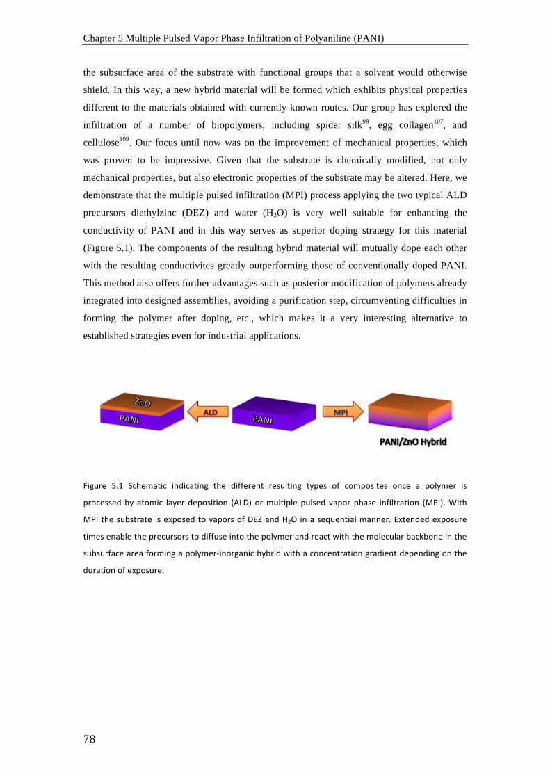
Chapter 5 Multiple Pulsed Vapor Phase Infiltration of Polyaniline (PANI)
78
the subsurface area of the substrate with functional groups that a solvent would otherwise
shield. In this way, a new hybrid material will be formed which exhibits physical properties
different to the materials obtained with currently known routes. Our group has explored the
infiltration of a number of biopolymers, including spider silk98, egg collagen107, and
cellulose109. Our focus until now was on the improvement of mechanical properties, which
was proven to be impressive. Given that the substrate is chemically modified, not only
mechanical properties, but also electronic properties of the substrate may be altered. Here, we
demonstrate that the multiple pulsed infiltration (MPI) process applying the two typical ALD
precursors diethylzinc (DEZ) and water (H2O) is very well suitable for enhancing the
conductivity of PANI and in this way serves as superior doping strategy for this material
(Figure 5.1). The components of the resulting hybrid material will mutually dope each other
with the resulting conductivites greatly outperforming those of conventionally doped PANI.
This method also offers further advantages such as posterior modification of polymers already
integrated into designed assemblies, avoiding a purification step, circumventing difficulties in
forming the polymer after doping, etc., which makes it a very interesting alternative to
established strategies even for industrial applications.
Figure 5.1 Schematic indicating the different resulting types of composites once a polymer is
processed by atomic layer deposition (ALD) or multiple pulsed vapor phase infiltration (MPI). With
MPI the substrate is exposed to vapors of DEZ and H2O in a sequential manner. Extended exposure
times enable the precursors to diffuse into the polymer and react with the molecular backbone in the
subsurface area forming a polymer-‐inorganic hybrid with a concentration gradient depending on the
duration of exposure.
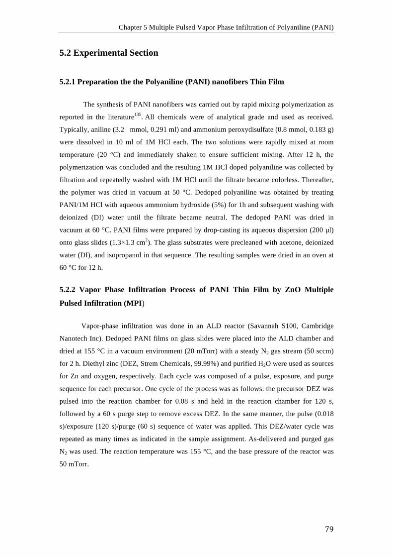
Chapter 5 Multiple Pulsed Vapor Phase Infiltration of Polyaniline (PANI)
79
5.2 Experimental Section
5.2.1 Preparation the the Polyaniline (PANI) nanofibers Thin Film
The synthesis of PANI nanofibers was carried out by rapid mixing polymerization as
reported in the literature135. All chemicals were of analytical grade and used as received.
Typically, aniline (3.2 mmol, 0.291 ml) and ammonium peroxydisulfate (0.8 mmol, 0.183 g)
were dissolved in 10 ml of 1M HCl each. The two solutions were rapidly mixed at room
temperature (20 °C) and immediately shaken to ensure sufficient mixing. After 12 h, the
polymerization was concluded and the resulting 1M HCl doped polyaniline was collected by
filtration and repeatedly washed with 1M HCl until the filtrate became colorless. Thereafter,
the polymer was dried in vacuum at 50 °C. Dedoped polyaniline was obtained by treating
PANI/1M HCl with aqueous ammonium hydroxide (5%) for 1h and subsequent washing with
deionized (DI) water until the filtrate became neutral. The dedoped PANI was dried in
vacuum at 60 °C. PANI films were prepared by drop-casting its aqueous dispersion (200 µl)
onto glass slides (1.3×1.3 cm2). The glass substrates were precleaned with acetone, deionized
water (DI), and isopropanol in that sequence. The resulting samples were dried in an oven at
60 °C for 12 h.
5.2.2 Vapor Phase Infiltration Process of PANI Thin Film by ZnO Multiple
Pulsed Infiltration (MPI)
Vapor-phase infiltration was done in an ALD reactor (Savannah S100, Cambridge
Nanotech Inc). Dedoped PANI films on glass slides were placed into the ALD chamber and
dried at 155 °C in a vacuum environment (20 mTorr) with a steady N2 gas stream (50 sccm)
for 2 h. Diethyl zinc (DEZ, Strem Chemicals, 99.99%) and purified H2O were used as sources
for Zn and oxygen, respectively. Each cycle was composed of a pulse, exposure, and purge
sequence for each precursor. One cycle of the process was as follows: the precursor DEZ was
pulsed into the reaction chamber for 0.08 s and held in the reaction chamber for 120 s,
followed by a 60 s purge step to remove excess DEZ. In the same manner, the pulse (0.018
s)/exposure (120 s)/purge (60 s) sequence of water was applied. This DEZ/water cycle was
repeated as many times as indicated in the sample assignment. As-delivered and purged gas
N2 was used. The reaction temperature was 155 °C, and the base pressure of the reactor was
50 mTorr.
Chapter 5 Multiple Pulsed Vapor Phase Infiltration of Polyaniline (PANI)
80
5.2.3 Characterization Fourier-transform infrared (FTIR) spectra of the samples were recorded between 750
and 1680 cm-1 with an FT-IR spectrometer (Frontier; PerkinElmer).
Morphology examination of the samples was done with a scanning electron
microscope (SEM, Quanta 250 FEG; FEI) at 10kV. Thickness measurements were carried out
on a cleaved cross-section of the sample by FEG-SEM.
Raman spectroscopy at 532 cm-1 excitation wavelength was performed with a Raman
microscope (Alpha 300S, WITec). The laser power was kept below 0.7 mW to avoid sample
degradation.
Absorption spectra of the samples were recorded between 375-960 nm using a UV-
Vis spectrophotometer (V-630 BIO, JASCO).
X-ray diffraction (XRD) analysis was carried with a powder diffractometer (X´pert,
with 45 kV, 40 mA; PANalytical) with Ni-filtered Cu Kα radiation.
XPS experiments were conducted using a PHOIBOS photoelectron spectrometer
equipped with an Al Kα X-ray source (12 mA, 8.33 kV) as the incident photon radiation, and
the spectra were standardized using the C1s peak at 284.6 eV.
TEM images were recorded and EDS analysis was carried out with an FEI Titan
microscope using 300 kV in scanning transmission electron microscopy mode and an EDAX
SDD detector. The focused ion beam (FIB) used for lamellae preparation was a dual beam
Helios Nanolab 450S from FEI. FIB lamellae were prepared from a Si wafer with the PANI
fibers deposited on it and after the entire wafer had undergone the ZnO MPI treatment. The
block was extracted by standard methods using a Pt electron beam deposition to initially
protect the sample surface before any ion beam deposition was carried out. The block was
thinned to transparency on a copper "Omniprobe" grid using a 5 kV gallium ion beam at 8 pA
for final surface preparation.
The conductivities of the thin films were measured applying a four-point probe
technique with a source measurement unit (Keithley 2611). For each experiment four or five
individual samples were tested for each MPI process cycle number. The resulting
conductivity, σ, was calculated according to the formula,
where I is the current, V is the voltage, and d is the polymer film thickness.
)( VI d/2ln πσ =
Chapter 5 Multiple Pulsed Vapor Phase Infiltration of Polyaniline (PANI)
81
5.3 Results and Discussion
5.3.1 Assessment of the electrical conductivity
After successful fabrication of dedoped PANI films supported on glass slides, the
samples were infiltrated with ZnO. In order to be able to identify the influence of infiltration
on the conductivity, a variety of processes have been applied and the results compared to
undoped and HCl doped PANI. While for a routine coating of a substrate by ALD a rather
short interaction of the vaporized precursor with the substrate surface is sufficient in order to
chemically bind the molecule, the infiltration strategy relies on the extension of the exposure
time and diffusion of the chemicals into subsurface areas. Therefore, we infiltrated samples
applying short and long exposure times as well as samples coated with ZnO without
infiltration. For this purpose, an initial layer of Al2O3 was deposited, which should act as an
infiltration barrier for the DEZ. In addition, we surveyed samples with various numbers of
infiltration cycles.
In Figure 5.2 (a) and (b) the room temperature I-V characteristics of the various PANI
samples with similar thicknesses (7 ~ 10 µm) are displayed, showing linear, ohmic behavior.
The electrical conductivity of the samples was calculated from the slopes of the I-V plots.
Figure 5.2 (c) and Table 1 give an overview over the conductivities of the various
investigated samples.
Chapter 5 Multiple Pulsed Vapor Phase Infiltration of Polyaniline (PANI)
82
Figure 5.2 (a) I-‐V plots of PANI doped with 1M HCl (reference) and PANI doped with ZnO with variable
numbers of infiltration cycles as indicated in the legend. The infiltration time for all the samples was
120 s per cycle. (b) I-‐V plots of PANI with a coating stack of Al2O3 (infiltration barrier)/ZnO, and PANI
doped with ZnO applying short (8 s) and long (120 s) exposure times. The number of cycles in all
samples was fixed to 200. (c) Comparison of conductivities of PANI after doping with HCl, coating with
ZnO and infiltration with ZnO with varying exposure times and cycle numbers.
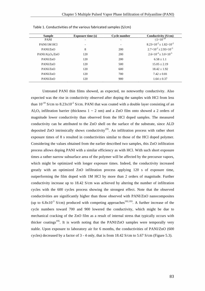
Chapter 5 Multiple Pulsed Vapor Phase Infiltration of Polyaniline (PANI)
83
Table 1. Conductivities of the various fabricated samples (S/cm)
Sample Exposure time (s) Cycle number Conductivity (S/cm) PANI - - ≤1×10⁻¹⁰
PANI/1M HCl - - 8.23×10⁻² ± 1.82×10⁻² PANI/ZnO 8 200 2.7×10⁻² ± 2.93×10⁻³
PANI/Al2O3/ZnO 120 200 2.6×10⁻⁴ ± 3.0×10⁻⁵ PANI/ZnO 120 200 6.58 ± 1.1 PANI/ZnO 120 500 15.05 ± 2.19 PANI/ZnO 120 600 18.42 ± 1.92 PANI/ZnO 120 700 7.42 ± 0.81 PANI/ZnO 120 900 1.64 ± 0.37
Untreated PANI thin films showed, as expected, no noteworthy conductivity. Also
expected was the rise in conductivity observed after doping the samples with HCl from less
than 10-10 S/cm to 8.23x10⁻² S/cm. PANI that was coated with a double layer consisting of an
Al2O3 infiltration barrier (thickness 1 ~ 2 nm) and a ZnO film onto showed a 2 orders of
magnitude lower conductivity than observed from the HCl doped samples. The measured
conductivity can be attributed to the ZnO shell on the surface of the substrate, since ALD
deposited ZnO intrinsically shows conductivity195. An infiltration process with rather short
exposure times of 8 s resulted in conductivities similar to those of the HCl doped polymer.
Considering the values obtained from the earlier described two samples, this ZnO infiltration
process allows doping PANI with a similar efficiency as with HCl. With such short exposure
times a rather narrow subsurface area of the polymer will be affected by the precursor vapors,
which might be optimized with longer exposure times. Indeed, the conductivity increased
greatly with an optimized ZnO infiltration process applying 120 s of exposure time,
outperforming the film doped with 1M HCl by more than 2 orders of magnitude. Further
conductivity increase up to 18.42 S/cm was achieved by altering the number of infiltration
cycles with the 600 cycles process showing the strongest effect. Note that the observed
conductivities are significantly higher than those observed with PANI/ZnO nanocomposites
(up to 6.8x10⁻³ S/cm) produced with competing approaches192,193. A further increase of the
cycle numbers toward 700 and 900 lowered the conductivity, which might be due to
mechanical cracking of the ZnO film as a result of internal stress that typically occurs with
thicker coatings195. It is worth noting that the PANI/ZnO samples were temporally very
stable. Upon exposure to laboratory air for 6 months, the conductivities of PANI/ZnO (600
cycles) decreased by a factor of 3 - 4 only, that is from 18.42 S/cm to 5.67 S/cm (Figure 5.3).
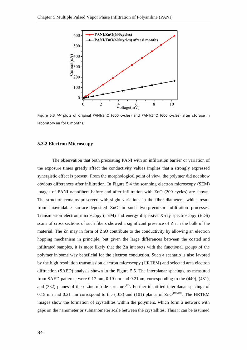
Chapter 5 Multiple Pulsed Vapor Phase Infiltration of Polyaniline (PANI)
84
Figure 5.3 I-‐V plots of original PANI/ZnO (600 cycles) and PANI/ZnO (600 cycles) after storage in
laboratory air for 6 months.
5.3.2 Electron Microscopy
The observation that both precoating PANI with an infiltration barrier or variation of
the exposure times greatly affect the conductivity values implies that a strongly expressed
synergistic effect is present. From the morphological point of view, the polymer did not show
obvious differences after infiltration. In Figure 5.4 the scanning electron microscopy (SEM)
images of PANI nanofibers before and after infiltration with ZnO (200 cycles) are shown.
The structure remains preserved with slight variations in the fiber diameters, which result
from unavoidable surface-deposited ZnO in such two-precursor infiltration processes.
Transmission electron microscopy (TEM) and energy dispersive X-ray spectroscopy (EDS)
scans of cross sections of such fibers showed a significant presence of Zn in the bulk of the
material. The Zn may in form of ZnO contribute to the conductivity by allowing an electron
hopping mechanism in principle, but given the large differences between the coated and
infiltrated samples, it is more likely that the Zn interacts with the functional groups of the
polymer in some way beneficial for the electron conduction. Such a scenario is also favored
by the high resolution transmission electron microscopy (HRTEM) and selected area electron
diffraction (SAED) analysis shown in the Figure 5.5. The interplanar spacings, as measured
from SAED patterns, were 0.17 nm, 0.19 nm and 0.21nm, corresponding to the (440), (431),
and (332) planes of the c-zinc nitride structure196. Further identified interplanar spacings of
0.15 nm and 0.21 nm correspond to the (103) and (101) planes of ZnO197,198. The HRTEM
images show the formation of crystallites within the polymers, which form a network with
gaps on the nanometer or subnanometer scale between the crystallites. Thus it can be assumed
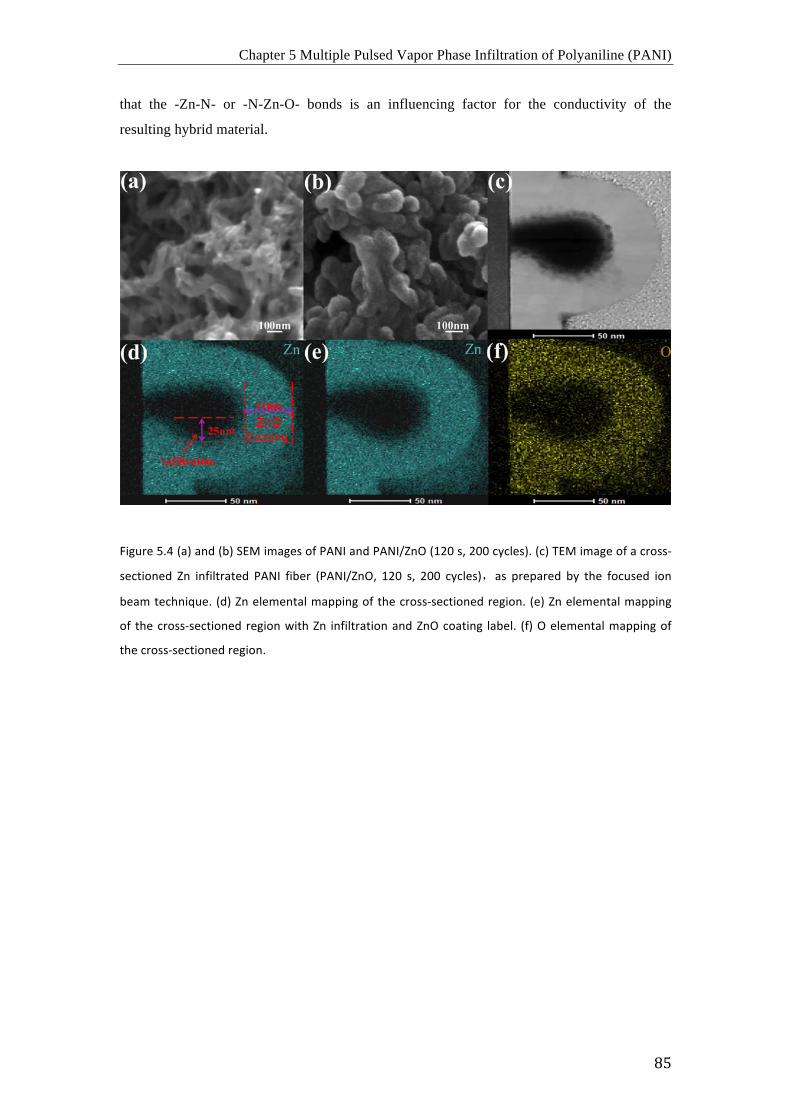
Chapter 5 Multiple Pulsed Vapor Phase Infiltration of Polyaniline (PANI)
85
that the -Zn-N- or -N-Zn-O- bonds is an influencing factor for the conductivity of the
resulting hybrid material.
Figure 5.4 (a) and (b) SEM images of PANI and PANI/ZnO (120 s, 200 cycles). (c) TEM image of a cross-‐
sectioned Zn infiltrated PANI fiber (PANI/ZnO, 120 s, 200 cycles),as prepared by the focused ion
beam technique. (d) Zn elemental mapping of the cross-‐sectioned region. (e) Zn elemental mapping
of the cross-‐sectioned region with Zn infiltration and ZnO coating label. (f) O elemental mapping of
the cross-‐sectioned region.
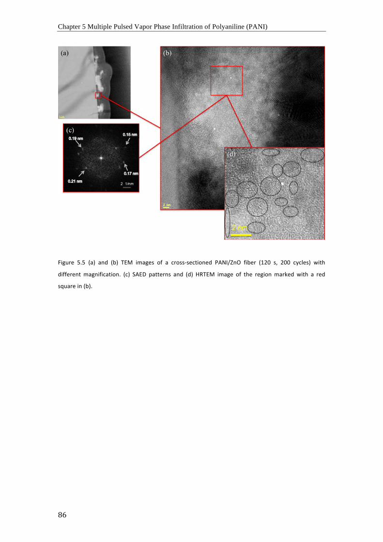
Chapter 5 Multiple Pulsed Vapor Phase Infiltration of Polyaniline (PANI)
86
Figure 5.5 (a) and (b) TEM images of a cross-‐sectioned PANI/ZnO fiber (120 s, 200 cycles) with
different magnification. (c) SAED patterns and (d) HRTEM image of the region marked with a red
square in (b).
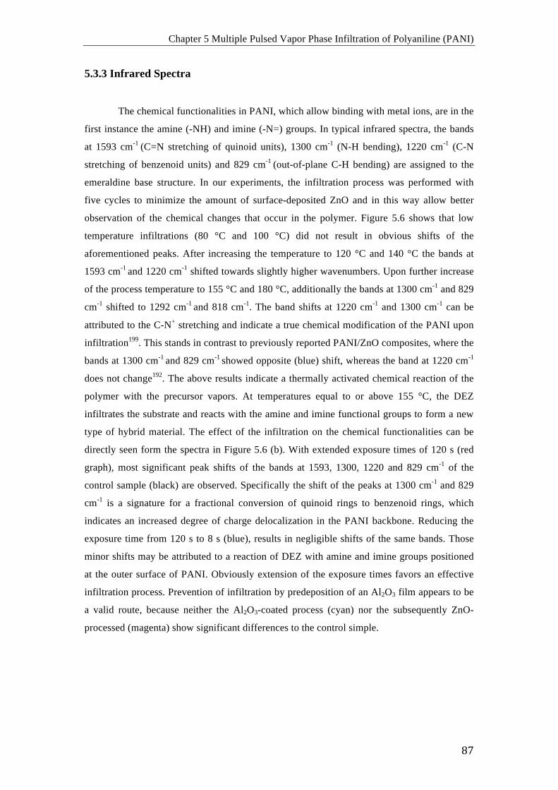
Chapter 5 Multiple Pulsed Vapor Phase Infiltration of Polyaniline (PANI)
87
5.3.3 Infrared Spectra
The chemical functionalities in PANI, which allow binding with metal ions, are in the
first instance the amine (-NH) and imine (-N=) groups. In typical infrared spectra, the bands
at 1593 cm-1 (C=N stretching of quinoid units), 1300 cm-1 (N-H bending), 1220 cm-1 (C-N
stretching of benzenoid units) and 829 cm-1 (out-of-plane C-H bending) are assigned to the
emeraldine base structure. In our experiments, the infiltration process was performed with
five cycles to minimize the amount of surface-deposited ZnO and in this way allow better
observation of the chemical changes that occur in the polymer. Figure 5.6 shows that low
temperature infiltrations (80 °C and 100 °C) did not result in obvious shifts of the
aforementioned peaks. After increasing the temperature to 120 °C and 140 °C the bands at
1593 cm-1 and 1220 cm-1 shifted towards slightly higher wavenumbers. Upon further increase
of the process temperature to 155 °C and 180 °C, additionally the bands at 1300 cm-1 and 829
cm-1 shifted to 1292 cm-1 and 818 cm-1. The band shifts at 1220 cm-1 and 1300 cm-1 can be
attributed to the C-N+ stretching and indicate a true chemical modification of the PANI upon
infiltration199. This stands in contrast to previously reported PANI/ZnO composites, where the
bands at 1300 cm-1 and 829 cm-1 showed opposite (blue) shift, whereas the band at 1220 cm-1
does not change192. The above results indicate a thermally activated chemical reaction of the
polymer with the precursor vapors. At temperatures equal to or above 155 °C, the DEZ
infiltrates the substrate and reacts with the amine and imine functional groups to form a new
type of hybrid material. The effect of the infiltration on the chemical functionalities can be
directly seen form the spectra in Figure 5.6 (b). With extended exposure times of 120 s (red
graph), most significant peak shifts of the bands at 1593, 1300, 1220 and 829 cm-1 of the
control sample (black) are observed. Specifically the shift of the peaks at 1300 cm-1 and 829
cm-1 is a signature for a fractional conversion of quinoid rings to benzenoid rings, which
indicates an increased degree of charge delocalization in the PANI backbone. Reducing the
exposure time from 120 s to 8 s (blue), results in negligible shifts of the same bands. Those
minor shifts may be attributed to a reaction of DEZ with amine and imine groups positioned
at the outer surface of PANI. Obviously extension of the exposure times favors an effective
infiltration process. Prevention of infiltration by predeposition of an Al2O3 film appears to be
a valid route, because neither the Al2O3-coated process (cyan) nor the subsequently ZnO-
processed (magenta) show significant differences to the control simple.
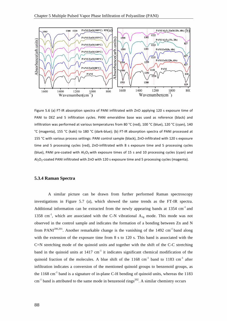
Chapter 5 Multiple Pulsed Vapor Phase Infiltration of Polyaniline (PANI)
88
Figure 5.6 (a) FT-‐IR absorption spectra of PANI infiltrated with ZnO applying 120 s exposure time of
PANI to DEZ and 5 infiltration cycles. PANI emeraldine base was used as reference (black) and
infiltration was performed at various temperatures from 80 °C (red), 100 °C (blue), 120 °C (cyan), 140
°C (magenta), 155 °C (kaki) to 180 °C (dark-‐blue); (b) FT-‐IR absorption spectra of PANI processed at
155 °C with various process settings: PANI control sample (black), ZnO-‐infiltrated with 120 s exposure
time and 5 processing cycles (red), ZnO-‐infiltrated with 8 s exposure time and 5 processing cycles
(blue), PANI pre-‐coated with Al2O3 with exposure times of 15 s and 10 processing cycles (cyan) and
Al2O3-‐coated PANI infiltrated with ZnO with 120 s exposure time and 5 processing cycles (magenta).
5.3.4 Raman Spectra
A similar picture can be drawn from further performed Raman spectroscopy
investigations in Figure 5.7 (a), which showed the same trends as the FT-IR spectra.
Additional information can be extracted from the newly appearing bands at 1354 cm-1 and
1358 cm-1, which are associated with the C-N vibrational A1g mode. This mode was not
observed in the control sample and indicates the formation of a bonding between Zn and N
from PANI200,201. Another remarkable change is the vanishing of the 1492 cm-1 band along
with the extension of the exposure time from 8 s to 120 s. This band is associated with the
C=N stretching mode of the quinoid units and together with the shift of the C-C stretching
band in the quinoid units at 1417 cm-1 it indicates significant chemical modification of the
quinoid fraction of the molecules. A blue shift of the 1168 cm-1 band to 1183 cm-1 after
infiltration indicates a conversion of the mentioned quinoid groups to benzenoid groups, as
the 1168 cm-1 band is a signature of in-plane C-H bending of quinoid units, whereas the 1183
cm-1 band is attributed to the same mode in benzenoid rings202. A similar chemistry occurs
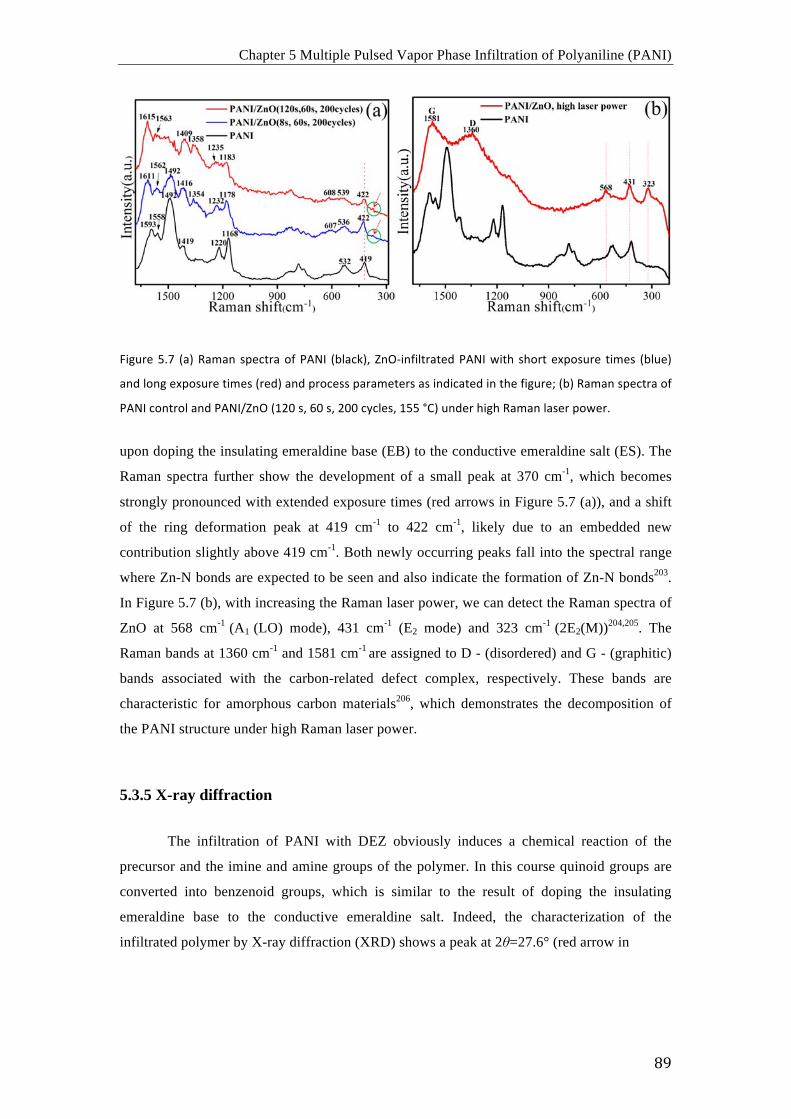
Chapter 5 Multiple Pulsed Vapor Phase Infiltration of Polyaniline (PANI)
89
Figure 5.7 (a) Raman spectra of PANI (black), ZnO-‐infiltrated PANI with short exposure times (blue)
and long exposure times (red) and process parameters as indicated in the figure; (b) Raman spectra of
PANI control and PANI/ZnO (120 s, 60 s, 200 cycles, 155 °C) under high Raman laser power.
upon doping the insulating emeraldine base (EB) to the conductive emeraldine salt (ES). The
Raman spectra further show the development of a small peak at 370 cm-1, which becomes
strongly pronounced with extended exposure times (red arrows in Figure 5.7 (a)), and a shift
of the ring deformation peak at 419 cm-1 to 422 cm-1, likely due to an embedded new
contribution slightly above 419 cm-1. Both newly occurring peaks fall into the spectral range
where Zn-N bonds are expected to be seen and also indicate the formation of Zn-N bonds203.
In Figure 5.7 (b), with increasing the Raman laser power, we can detect the Raman spectra of
ZnO at 568 cm-1 (A1 (LO) mode), 431 cm-1 (E2 mode) and 323 cm-1 (2E2(M))204,205. The
Raman bands at 1360 cm-1 and 1581 cm-1 are assigned to D - (disordered) and G - (graphitic)
bands associated with the carbon-related defect complex, respectively. These bands are
characteristic for amorphous carbon materials206, which demonstrates the decomposition of
the PANI structure under high Raman laser power.
5.3.5 X-ray diffraction
The infiltration of PANI with DEZ obviously induces a chemical reaction of the
precursor and the imine and amine groups of the polymer. In this course quinoid groups are
converted into benzenoid groups, which is similar to the result of doping the insulating
emeraldine base to the conductive emeraldine salt. Indeed, the characterization of the
infiltrated polymer by X-ray diffraction (XRD) shows a peak at 2θ=27.6° (red arrow in
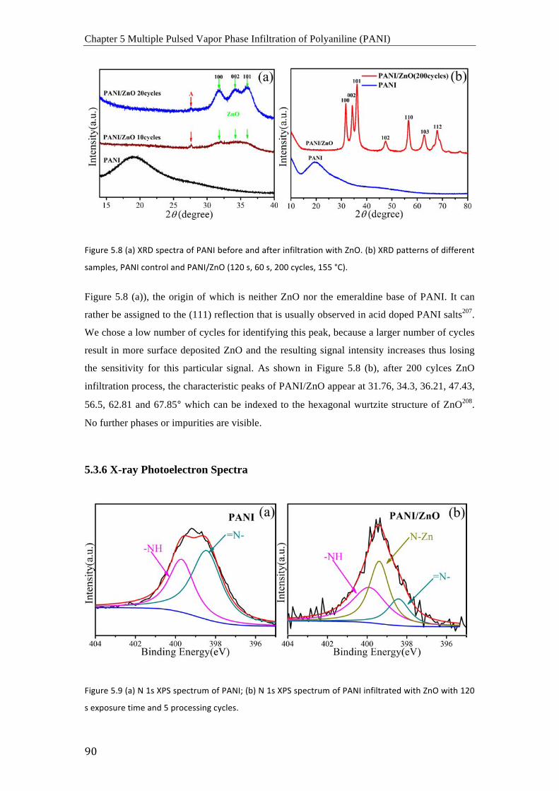
Chapter 5 Multiple Pulsed Vapor Phase Infiltration of Polyaniline (PANI)
90
Figure 5.8 (a) XRD spectra of PANI before and after infiltration with ZnO. (b) XRD patterns of different
samples, PANI control and PANI/ZnO (120 s, 60 s, 200 cycles, 155 °C).
Figure 5.8 (a)), the origin of which is neither ZnO nor the emeraldine base of PANI. It can
rather be assigned to the (111) reflection that is usually observed in acid doped PANI salts207.
We chose a low number of cycles for identifying this peak, because a larger number of cycles
result in more surface deposited ZnO and the resulting signal intensity increases thus losing
the sensitivity for this particular signal. As shown in Figure 5.8 (b), after 200 cylces ZnO
infiltration process, the characteristic peaks of PANI/ZnO appear at 31.76, 34.3, 36.21, 47.43,
56.5, 62.81 and 67.85° which can be indexed to the hexagonal wurtzite structure of ZnO208.
No further phases or impurities are visible.
5.3.6 X-ray Photoelectron Spectra
Figure 5.9 (a) N 1s XPS spectrum of PANI; (b) N 1s XPS spectrum of PANI infiltrated with ZnO with 120
s exposure time and 5 processing cycles.
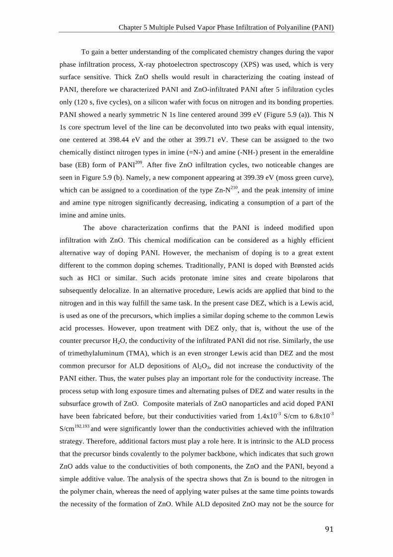
Chapter 5 Multiple Pulsed Vapor Phase Infiltration of Polyaniline (PANI)
91
To gain a better understanding of the complicated chemistry changes during the vapor
phase infiltration process, X-ray photoelectron spectroscopy (XPS) was used, which is very
surface sensitive. Thick ZnO shells would result in characterizing the coating instead of
PANI, therefore we characterized PANI and ZnO-infiltrated PANI after 5 infiltration cycles
only (120 s, five cycles), on a silicon wafer with focus on nitrogen and its bonding properties.
PANI showed a nearly symmetric N 1s line centered around 399 eV (Figure 5.9 (a)). This N
1s core spectrum level of the line can be deconvoluted into two peaks with equal intensity,
one centered at 398.44 eV and the other at 399.71 eV. These can be assigned to the two
chemically distinct nitrogen types in imine (=N-) and amine (-NH-) present in the emeraldine
base (EB) form of PANI209. After five ZnO infiltration cycles, two noticeable changes are
seen in Figure 5.9 (b). Namely, a new component appearing at 399.39 eV (moss green curve),
which can be assigned to a coordination of the type Zn-N210, and the peak intensity of imine
and amine type nitrogen significantly decreasing, indicating a consumption of a part of the
imine and amine units.
The above characterization confirms that the PANI is indeed modified upon
infiltration with ZnO. This chemical modification can be considered as a highly efficient
alternative way of doping PANI. However, the mechanism of doping is to a great extent
different to the common doping schemes. Traditionally, PANI is doped with Brønsted acids
such as HCl or similar. Such acids protonate imine sites and create bipolarons that
subsequently delocalize. In an alternative procedure, Lewis acids are applied that bind to the
nitrogen and in this way fulfill the same task. In the present case DEZ, which is a Lewis acid,
is used as one of the precursors, which implies a similar doping scheme to the common Lewis
acid processes. However, upon treatment with DEZ only, that is, without the use of the
counter precursor H2O, the conductivity of the infiltrated PANI did not rise. Similarly, the use
of trimethylaluminum (TMA), which is an even stronger Lewis acid than DEZ and the most
common precursor for ALD depositions of Al2O3, did not increase the conductivity of the
PANI either. Thus, the water pulses play an important role for the conductivity increase. The
process setup with long exposure times and alternating pulses of DEZ and water results in the
subsurface growth of ZnO. Composite materials of ZnO nanoparticles and acid doped PANI
have been fabricated before, but their conductivities varied from 1.4x10⁻³ S/cm to 6.8x10⁻³
S/cm192,193 and were significantly lower than the conductivities achieved with the infiltration
strategy. Therefore, additional factors must play a role here. It is intrinsic to the ALD process
that the precursor binds covalently to the polymer backbone, which indicates that such grown
ZnO adds value to the conductivities of both components, the ZnO and the PANI, beyond a
simple additive value. The analysis of the spectra shows that Zn is bound to the nitrogen in
the polymer chain, whereas the need of applying water pulses at the same time points towards
the necessity of the formation of ZnO. While ALD deposited ZnO may not be the source for
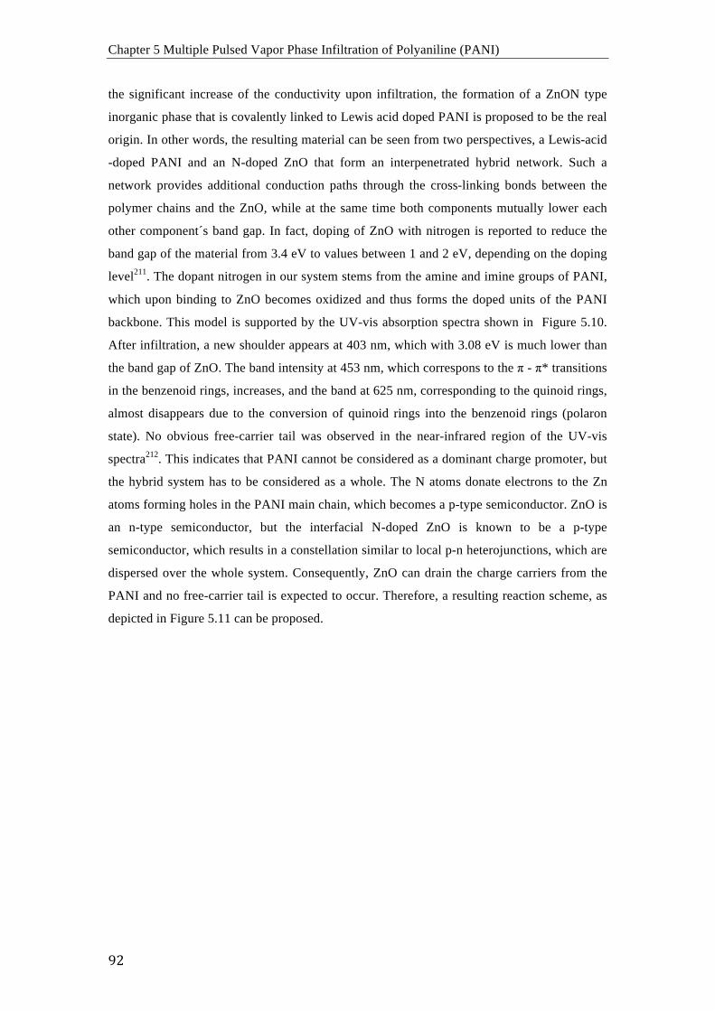
Chapter 5 Multiple Pulsed Vapor Phase Infiltration of Polyaniline (PANI)
92
the significant increase of the conductivity upon infiltration, the formation of a ZnON type
inorganic phase that is covalently linked to Lewis acid doped PANI is proposed to be the real
origin. In other words, the resulting material can be seen from two perspectives, a Lewis-acid
-doped PANI and an N-doped ZnO that form an interpenetrated hybrid network. Such a
network provides additional conduction paths through the cross-linking bonds between the
polymer chains and the ZnO, while at the same time both components mutually lower each
other component´s band gap. In fact, doping of ZnO with nitrogen is reported to reduce the
band gap of the material from 3.4 eV to values between 1 and 2 eV, depending on the doping
level211. The dopant nitrogen in our system stems from the amine and imine groups of PANI,
which upon binding to ZnO becomes oxidized and thus forms the doped units of the PANI
backbone. This model is supported by the UV-vis absorption spectra shown in Figure 5.10.
After infiltration, a new shoulder appears at 403 nm, which with 3.08 eV is much lower than
the band gap of ZnO. The band intensity at 453 nm, which correspons to the π - π* transitions
in the benzenoid rings, increases, and the band at 625 nm, corresponding to the quinoid rings,
almost disappears due to the conversion of quinoid rings into the benzenoid rings (polaron
state). No obvious free-carrier tail was observed in the near-infrared region of the UV-vis
spectra212. This indicates that PANI cannot be considered as a dominant charge promoter, but
the hybrid system has to be considered as a whole. The N atoms donate electrons to the Zn
atoms forming holes in the PANI main chain, which becomes a p-type semiconductor. ZnO is
an n-type semiconductor, but the interfacial N-doped ZnO is known to be a p-type
semiconductor, which results in a constellation similar to local p-n heterojunctions, which are
dispersed over the whole system. Consequently, ZnO can drain the charge carriers from the
PANI and no free-carrier tail is expected to occur. Therefore, a resulting reaction scheme, as
depicted in Figure 5.11 can be proposed.
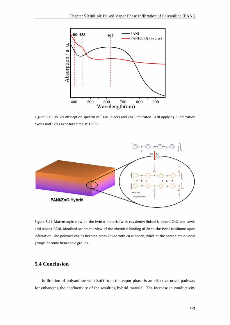
Chapter 5 Multiple Pulsed Vapor Phase Infiltration of Polyaniline (PANI)
93
Figure 5.10 UV-‐Vis absorption spectra of PANI (black) and ZnO-‐infiltrated PANI applying 5 infiltration
cycles and 120 s exposure time at 155 °C.
Figure 5.11 Macroscopic view on the hybrid material with covalently linked N-‐doped ZnO and Lewis
acid doped PANI. Idealized schematic view of the chemical binding of Zn to the PANI backbone upon
infiltration. The polymer chains become cross-‐linked with Zn-‐N bonds, while at the same time quinoid
groups become benzenoid groups.
5.4 Conclusion
Infiltration of polyaniline with ZnO from the vapor phase is an effective novel pathway
for enhancing the conductivity of the resulting hybrid material. The increase in conductivity
Chapter 5 Multiple Pulsed Vapor Phase Infiltration of Polyaniline (PANI)
94
that is observed after successful processing goes significantly beyond the additive
contribution to the conductivity provided by the individual components. The reason for such
improvement is considered to lie in a synergistic mutual doping of both the inorganic and the
polymeric constituent of the hybrid material. Vapor phase infiltration enforces binding of Zn
to the nitrogen present in the polymer backbone, which induces Lewis acid type of doping of
PANI, whereas at the same time the ZnO becomes doped with nitrogen. The interpenetrated
network further provides additional conduction pathways through cross-linking of the
polymer chains with the inorganic material, additionally contributing to an enhanced
conductivity. Although the process was demonstrated on one particular substrate-precursor
system, the principle may be extended to further material couples as well. While a large
variety of semiconducting polymers, all of which contain functional chemical groups of
different types, is available, the vapor phase infiltration process can easily be applied for the
development of a plethora of further material combinations.
95
Chapter 6
Summary and Outlook
This thesis presents strategies for the ALD-derived vapor phase infiltration (VPI) and
doping process of the conducting polymers polyaniline (PANI) and poly(3-hexyl)thiophene
(P3HT). It can be divided into three parts: 1) single precursor (MoCl5 or SnCl4) vapor phase
infiltration and doping of PANI; 2) single precursor (MoCl5) vapor phase infiltration and
doping of P3HT; 3) multiple pulsed (diethylzinc (DEZ) and H2O) vapor phase infiltration and
doping of PANI.
In the first part, a novel way of doping PANI by an ALD-derived single precursor
VPI process was successfully demonstrated. This way not only allows to enhance the
conductivity of PANI by up to 6 orders of magnitude, but also to control the conductivity
through the choice and amount of the infiltrated precursor. More importantly, the conductivity
of the PANI doped in our way was barely affected by the thermal treatment at 150 °C in
vacuum, while the conductivity of the 1M HCl doped PANI was almost completely lost. This
loss is due to a deprotonation of the doped PANI and resulting evaporation of HCl. Doping
with MoCl5 or SnCl4 can result in an oxidation of the PANI and very likly in a complexation
of the metal chlorides with the nitrogen in PANI. As a result, the electron mobility along the
polymer chains was significantly enhanced and the structure was stabilized even at elevated
temperatures.
In the second part, the ALD-derived single precursor VPI process was used to dope
the conducting polymer P3HT. After the MoCl5 infiltration process, the conductivity of P3HT
rose up to 5 orders of magnitude. The P3HT/MoCl5 thin film showed exceptional stability
under ambient conditions, largely outperforming the stability of the reported doped
P3HT/FTS. Doping with MoCl5 from the vapor phase results in a local oxidation of the
P3HT. The lone electron pairs at the sulfur atoms of the thiophene rings in P3HT can donate
negative charge to the MoCl5 with themselves becoming rather positively charged. The results
are not only significant for the novel process to dope P3HT and obtain better stabilily, but
also for the possibility of performing top-down doping of already pre-manufactured P3HT,
which allows for better shaping of the material and therefore more efficient device
fabrication.
Chapter 6 Summary and Outlook
96
In the last part, the multiple pulsed (DEZ and H2O) vapor phase infiltration and
doping of PANI was studied. The infiltration of PANI with ZnO from the vapor phase is an
effective novel pathway for increasing the conductivity of the resulting hybrid material. The
increase in conductivity was up to 3 orders of magnitude higher than upon conventional
doping with 1 M HCl in wet chemical ways. The reason for the conductivity improvement is
likely due to a synergistic mutual doping of both the inorganic and the organic polymeric
constituent of the hybrid material. Vapor phase infiltration enforces binding of Zn to the
nitrogen present in the polymer backbone, which induces Lewis acid type of doping of PANI,
while at the same time the ZnO becomes doped with nitrogen. The interpenetrated network
further provides additional conduction pathways through crosslinking of the polymer chains
with inorganic material, which results in the increased conductivity.
In conclusion, for avoiding the negative influence of the wet chemical doping
approaches, the research performed in this thesis successfully demonstrated a novel way of
doping conducting polymers, by applying an ALD-derived vapor phase infiltration (VPI) and
doping porcess. The VPI process not only allows efficient control in the doping level, but also
allows solvent-free processing and even top-down doping of already manufactured and
shaped conducting polymers. It can be foreseen that the results presented in this work will be
further improved in future work, considering the vast amount of conductive polymers known
and the equally vast amount of ALD processes that are developed and can be used for an
infiltration process. The present work may therefore act as seminal work for future
developments of conductive polymers.
97
Bibliography (1) MacDiarmid, A. G. ¨Synthetic Metals¨: A Novel Role for Organic polymers (Nobel lecture). Angew. Chem. Int. Ed. 2001, 40, 2581−2590. (2) Li, Y. F. Organic Optoelectronic Materials. Lecture Notes in Chemistry 2015, 91, ISBN 978-3-319-16862-3. (3) Chiang, C. K.; Fincher, C. R.; Park, Y. W.; Heeger, A. J.; Shirakawa, H.; Louis, E. J.; Gau, S. C.; MacDiarmid, A. G. Electrical Conductivity in Doped Polyacetylene. Phys. Rev. Lett. 1977, 39, 1098-1101. (4) Chiang, C. K.; Druy, M. A.; Gau, S. C.; Heeger, A. J.; Louis, E. J.; MacDiarmid, A. G.; Park, Y. W.; Shirakawa, H. Synthesis of Highly Conducting Films of Derivatives of Polyacetylene, (CH)x. J. Am. Chem. Soc., 1978, 100, 1013–1015. (5) Handbook of Organic Conductive Materials and Polymers (Ed.: H. S. Nalwa), Wiley, New York, 1997; Handbook of Conducting Polymers (Ed.: T. A. Skotheim, R. L. Elsenbaumer, J. F. Reynolds), 2nd ed., Marcel Dekker, New York, 1998. (6) Yu, G.; Gao, J.; Hummelen, J. C.; Wudl, F.; Heeger, A. J. Polymer Photovoltaic Cells: Enhanced Efficiencies via a Network of Internal Donor-Acceptor Heterojunctions. Science 1995, 270, 1789-1791. (7) Zhao, W., Qian, D., Zhang, S., Li, S., Inganäs, O., Gao, F. and Hou, J. Fullerene-free polymer solar cells with over 11% efficiency and excellent thermal stability. Adv. Mater. 2016, 28, 4734–4739. (8) Vandewal, K., Widmer, J., Heumueller, T., Brabec, C. J., McGehee, M. D., Leo, K., Riede, M. and Salleo, A. Increased open-circuit voltage of organic solar cells by reduced donor-acceptor interface area. Adv. Mater. 2014, 26, 3839–3843. (9) Poelking, C., Tietze, M., Elschner, C., Olthof, S., Hertel, D., Baumeier, B., Wurthner, F.; Meerholz, K.; Leo, K.; Andrienko, D. Impact of mesoscale order on open-circuit voltage in organic solar cells. Nat. Mater. 2014, 14, 434–439. (10) Tang, C. W. Two-layer organic photovoltaic cell. Appl. Phys. Lett. 1986, 48, 183–185. (11) Cao, W. R.; Xue, J. G. Recent progress in organic photovoltaics: device architecture and optical design. Energy Environ. Sci., 2014, 7, 2123-2144 (12) Kippelen, B.; Brédas, J. L. Organic photovoltaics. Energy Environ. Sci., 2009, 2, 251-261. (13) Bundgaard, E.; Krebs, F. C. Low band gap polymers for organic photovoltaics. Solar Energy Materials and Solar Cells, 2007, 91, 954-985. (14) Hu, L. B.; Gruner, G.; Li, D.; Kaner, R. B.; Cech, J. Patternable transparent carbon nanotube films for electrochromic devices. J. Appl. Phys. 2007, 101, 016102.
Bibliography
98
(15) Tsai, T. S.; Pillay, V.; Choonara, Y. E.; Toit, L. C.; Modi, G.; Naidoo, D.; Kumar, P. A Polyvinyl Alcohol-Polyaniline Based Electro-Conductive Hydrogel for Controlled Stimuli-Actuable Release of Indomethacin. Polymers 2011, 3, 150-172. (16) Anderson, M. R.; Mattes, B. R.; Reiss, H.; Kaner, R. B. Conjugated Polymer Films for Gas Separation. Science 1991, 252, 1412-1415. (17) Huang, J. X.; Virji, S.; Weiller, B. H.; Kaner, R. B. Polyaniline Nanofibers: Facile Synthesis and Chemical Sensors. J. Am. Chem. Soc. 2003, 125, 314–315. (18) Li, D.; Mueller, M. B.; Gilje, S.; Kaner, R. B.; Wallace, G. G. Conjugated Polymer-based chemical sensors. Chem. Rev. 2000, 100, 2537-2574. (19) Huang, J.; Virji, S.; Weiller, B. H.; Kaner, R. B. Nanostructured Polyaniline Sensors. Chem. - Eur. J. 2004, 10, 1315–1319. (20) Karami, H.; Mousavi, M. F.; Shamsipur, M. A new design for dry polyaniline rechargeable batteries. Journal of Power Sources, 2003, 117, 255-259. (21) MacDiarmid, A. G.; Yang, L. S.; Huang, W. S.; Humphrey, B. D. Polyaniline: Electrochemistry and application to rechargeable batteries. Synthetic Metals, 1987, 18, 383-398. (22) Zhou, Q.; Shi, G. Conducting Polymer-Based Catalysts. J. Am. Chem. Soc. 2016, 138, 2868−2876. (23) Shi, Y., Peng, L.; Ding, Y.; Zhao, Y.; Yu, G. Nanostructured Conductive Polymers for Advanced Energy Storage. Chem. Soc. Rev., 2015, 44, 6684-6696. (24) Das, D.; Datta, A.; Contractor, A. Q. Doping of Polyaniline with 6‑Cyano-2-naphthol. J. Phys. Chem. B 2014, 118, 12993−13001. (25) Li, D.; Huang, J. X.; Kaner, R. B. Polyaniline Nanofibers: A Unique Polymer Nanostructure for Versatile Applications. Accounts of Chemical Research, 2009, 42, 135-145. (26) Groenendaal, L.; Jonas, F.; Freitag, D.; Peilartzik, H.; Reynolds, J. R. Poly(3,4-ethylenedioxythiophene) and Its Derivatives: Past, Present, and Future. Adv. Mater., 2000, 12, 481–494. (27) Cao, Y.; Yu, G.; Menon, R.; Heeger, A. J. Polymer Light-emitting Diodes with Polyethylene Dioxythiophene–polystyrene Sulfonate as the Transparent Anode. Synthetic Metals, 1997, 87, 171-174. (28) Lang, U.; Müller, E.; Naujoks, N.; Dual, J. Microscopical Investigations of PEDOT:PSS Thin Films. Adv. Funct. Mater., 2009, 19, 1215–1220. (29) Kim, J. Y.; Jung, J. H.; Lee, D. E.; Joo, J.Enhancement of Electrical Conductivity of Poly(3,4-ethylenedioxythiophene)/Poly(4-styrenesulfonate) by a Change of Solvents. Synth. Met. 2002, 126, 311-316. (30) Nardes, A. M.; Janssen, R. A. J.; Kemerink, M. A Morphological Model for the Solvent-Enhanced Conductivity of PEDOT:PSS Thin Films. Adv. Funct. Mater., 2008, 18, 865–871.
Bibliography
99
(31) Dobbelin, M.; Marcilla, R.; Salsamendi, M.; Pozo-Gonzalo, C.; Carrasco, P. M.; Pomposo, J. A.; Mecerreyes, D. Influence of Ionic Liquids on the Electrical Conductivity and Morphology of PEDOT:PSS Films. Chem. Mater., 2007, 19, 2147–2149. (32) Xia, Y.; Ouyang, J. Significant Conductivity Enhancement of Conductive Poly(3,4-ethylenedioxythiophene): Poly(styrenesulfonate) Films through a Treatment with Organic Carboxylic Acids and Inorganic Acids. ACS Appl. Mater. Interfaces, 2010, 2, 474–483. (33) Kim, Y. H.; Sachse, C.; Machala, M. L.; May, C.; Müller-Meskamp, L.; Leo, K. Highly Conductive PEDOT:PSS Electrode with Optimized Solvent and Thermal Post-Treatment for ITO-Free Organic Solar Cells. Adv. Funct. Mater., 2011, 21, 1076–1081. (34) Xia, Y.; Ouyang, J. Anion Effect on Salt-induced Conductivity Enhancement of Poly(3,4-ethylenedioxythiophene):poly(styrenesulfonate) Films. Organic Electronics 2010, 11, 1129-1135. (35) Xia, Y.; Sun, K.; Ouyang, J. Highly Conductive Poly(3,4-ethylenedioxythiophene):poly(styrene sulfonate) Films Treated with an Amphiphilic Fluoro Compound as the Transparent Electrode of Polymer Solar Cells. Energy Environ. Sci., 2012, 5, 5325-5332. (36) Alemu, D.; Wei, H. Y.; Ho, K. C.; Chu, C. W. Highly Conductive PEDOT:PSS Electrode by Simple Film Treatment with Methanol for ITO-free Polymer Solar Cells. Energy Environ. Sci., 2012, 5, 9662-9671. (37) Xia, Y.; Ouyang, J. Significant Different Conductivities of the Two Grades of Poly(3,4-ethylenedioxythiophene):Poly(styrenesulfonate), Clevios P and Clevios PH1000, Arising from Different Molecular Weights. ACS Appl. Mater. Interfaces, 2012, 4, 4131–4140. (38) Xia, Y.; Sun, K.; Ouyang, J. Solution-Processed Metallic Conducting Polymer Films as Transparent Electrode of Optoelectronic Devices. Adv. Mater., 2012, 24, 2436–2440. (39) Wang, G. M.; Swensen, J.; Moses, D.; Heeger, A. J. Increased Mobility from Regioregular Poly(3-hexylthiophene) Field-effect Transistors. Journal of Applied Physics 2003, 93, 6137-6141. (40) Moreas, F.; Schaffer, H.; Kobayashi, M.; Heeger, A. J.; Wudl, F. Photoexcitations in Poly(thiophene): Photoinduced Infrared Absorption and Photoinduced Electron-spin Resonance. Phys. Rev. B 1984, 30, 2948-2950. (41) Sirringhaus, H.; Brown, P. J.; Friend, R. H.; Nielsen, M. M.; Bechgaard, K.; Langeveld-Voss, B. M. M.; Spiering, A. J. H.; Janssen, R. A. J.; Meijer, E. W.; Herwig, P.; de Leeuw, D. M. Two-dimensional Charge Transport in Self-organized, High-mobility Conjugated Polymers. Nature 1999, 401, 685-688. (42) Sterbacka, R. O.; An, C. P.; Jiang, X. M.; Vardeny, Z. V. Two-Dimensional Electronic Excitations in Self-Assembled Conjugated Polymer Nanocrystals. Science 2000, 287, 839-842. (43) Bredas, J. L.; Street, G. B. Polarons, Bipolarons, and Solitons in Conducting Polymers. Acc. Chem. Res., 1985, 18, 309–315. (44) Roth, S.; Carroll, D. One Dimensional Metals, Second Edition. WILEY-VCH Verlag GmbH & Co. KGaA, Weinheim, 2004. ISBN: 3-527-30794-4.
Bibliography
100
(45) Stafstrom, S.; Chao, K. A. Soliton States in Polyacetylene. Pysical Review B 1984, 29, 2255-2266. (46) Su, W. P.; Schrieffer, J. R. Soliton Dynamics in Polyacetylene. Proceedings of the National Academy of Sciences of the United States of America 1980, 77, 5626-5629. (47) Heeger, A. J. Semiconduting and Metallic Polumers: The Fourth Generation of Polymeric Materials. J. Phys. Chem. B, 2001, 105, 8475-8491. (48) Sze, S. M. & Ng, K. K. Physics of Semiconductor Devices (Wiley-Interscience, 2006). (49) Méndez H,; Heimel G,; Winkler S,; Frisch J,; Opitz A,; Sauer K,; Wegner B,; Oehzelt M,; Röthel C,; Duhm S,; Többens D,; Koch N,; Salzmann I. Charge-transfer Crystallites as Molecular Electrical Dopants. Nature Communications, 2015, 6:8560. (50) Chiang, C. K.; Gau, S. C.; Fincher, C. R.; Park, Y. W.; MacDiarmid, A. G.; Heeger, A. J. Appl. Phys. Lett. 1978, 33, 18. (51) Shirakawa, H.; Louis, E. J.; MacDiarmid, A. G.; Chiang, C. K.; Heeger, A. J. Synthesis of Electrically Conducting Organic Polymers: Halogen Derivatives of Polyacetylene, (CH)x. J. Chem. Soc., Chem. Commun., 1977, 16, 578-580. (52) Ziemelis, K. E.; Hussain, A. T.; Bradley, D. D. C.; Friend, R. H.; Rühe, J.; Wegner, G. Optical Spectroscopy of Field-induced Charge in Poly(3-hexyl thienylene) Metal-insulator-semiconductor Structures: Evidence for Polarons. Phys. Rev. Lett. 1991, 66, 2231 (53) Handbook of Conducting Polymers, Vol 1&2 (Ed.: T. A. Skotheim) Marcel Dekker, New York, 1986. (54) Kanatzidis, M. G. Conductive Polymers, Chem. Eng. News 1990, 68, 36-50. (55) Nigrey, P. J.; MacDiarmid, A. G.; Heeger, A. J. Electrochemistry of Polyacetylene, (CH)x: Electrochemical Doping of (CH)x films to the Metallic State. Chem. Commun.1979, 96, 594-595. (56) MacInnes, D.; Druy, M. A.; Nigrey, P. J.; Nairns, D. P.; MacDiarmid, A. G.; Heeger, Organic Batteries: Reversible n- and p- Type Electrochemical Doping of Polyacetylene, (CH)x. A. J. J. Chem. Soc. Chem. Commun. 1981, 7, 317-319. (57) Salaneck, W. R.; Lundstrom, I.; Haung, W. S.; MacDiarmid, A. G. A Two-Dimensional-surface ‘State Diagram’ for Polyaniline. Synth. Met. 1986, 13, 291-297. (58) Chiang, J. C.; MacDiarmid, A. G. Polyaniline’: Protonic acid doping of the emeraldine form to the metallic regime. Synth. Met. 1986, 13, 193-205. (59) MacDiarmid, A. G.; Epstein, A. J. Polyanilines: a novel class of conducting polymers. Faraday Discuss. Chem. Soc. 1989, 88, 317-332. (60) MacDiarmid, A. G.; Epstein, A. J. Science and Applications of Conducting Polymers (Eds.:W. R. Salaneck, D. T. Clark, E. J. Samuelsen), Adam Hilger, Bristol, 1990, p. 117. (61) MacDiarmid, A. G.; Epstein, A. J. In Conjugated Polymeric Materials: Opportunities in Electronics, Optical Electronics and Molecular Electronics; Bredasand, J. L., Chance, R. R., Eds.; Kluwer Academic Publishers: Dordrecht, The Netherlands, 1990, p. 53.
Bibliography
101
(62) Wudl, F.; Angus, R. O.; Lu, F. L.; Allemand, P. M.; Vachon, D. J.; Nowak, M.; Liu, Z. X.; Heeger, A. J. Poly-p-phenyleneamineimine: Synthesis and Ccomparison to Polyaniline. J. Am. Chem. Soc. 1987, 109, 3677-3684. (63) Heeger, A. J.; Kivelson, S.; Schrieffer, J. R.; Su, W. P. Solitons in conducting polymers. Rev. Mod. Phys.1988, 60, 781-849. (64) Burroughes, J. H.; Jones, C. A.; Friend, R. H. New Semiconductor Device Physics in Polymer Diodes and Transistors. Nature 1988, 335, 137-141. (65) Burroughes, J. H.; Bradley, D. D. C.; Brown, A. R.; Marks, R. N.; Mackay, K.; Friend, R. H.; Burns, P. L.; Holmes, A. B. Light-emitting Diodes Based on Conjugated Polymers. Nature 1990, 347, 539-541. (66) Adinolfi, V.; Sargent, E. H. Photovoltage Field-effect Transistors. Nature 2017, 542, 324–327. (67) Tsao, H. N.; Cho, D. M.; Park, I.; Hansen, M. R.; Mavrin, A. Ultrahigh Mobility in Polymer Field-Effect Transistors by Design. J. Am. Chem. Soc., 2011, 133, 2605–2612. (68) Knopfmacher, O.; Hammock, M. L.; Appleton, A. L.; Schwartz, G.; Mei, J.; Lei, T.; Pei, J.; Bao, Z. Highly Stable Organic Polymer Field-effect Transistor Sensor for Selective Detection in the Marine Environment. Nat Commun. 2014, 5:2954. (69) Chang, M. H.; Das, D.; Varde, P.V.; Pecht, M. Light Emitting Diodes Reliability Review. Microelectronics Reliability 2012, 52, 762-782. (70) Kalyani, N. T.; Dhoble, S. J. Organic Light Emitting Diodes: Energy Saving Lighting Technology—A review. Renewable and Sustainable Energy Reviews 2012, 16, 2696-2723. (71) Jou, J. H.; Kumar, S.; Agrawal, A.; Li, T. H.; Sahoo, S. Approaches for Fabricating High Efficiency Organic Light Emitting Diodes. J. Mater. Chem. C, 2015, 3, 2974-3002. (72) Mazzio, K. A.; Luscombe, C. K. The Future of Organic Photovoltaics. Chem. Soc. Rev., 2015, 44, 78-90. (73) Lu, L.; Kelly, M. A.; You, W.; Yu, L. Status and Prospects for Ternary Organic Photovoltaics. Nature Photonics 2015, 9, 491–500. (74) Yao, H.; Ye, L.; Zhang, H.; Li, S.; Zhang, S.; Hou, J. Molecular Design of Benzodithiophene-Based Organic Photovoltaic Materials. Chem. Rev., 2016, 116, 7397–7457. (75) Leng, C. Z.; Losego, M. D. Vapor Phase Infiltration (VPI) for Transforming Polymers into Organic-inorganic Hybrid Materials: Current Progress and Future Chanllenges. Journal of Materials Horizons, 2017, 4, 747-771. (76) Knez, M.; Nielsch, K.; Niinistö, L. Synthesis and Surface Engineering of Complex Nanostructures by Atomic Layer Deposition. Adv. Mater., 2007, 19, 3425–3438. (77) George, S. M. Atomic Layer Depositon: An Overview. Chem. Rev., 2010, 110, 111–131. (78) Suntola, T.; Antson, J. Method for producing compound thin films. Google Patents; 1977.
Bibliography
102
(79) Suntola, T. Atomic Layer Epitaxy. Mater. Sci. Rep. 1989, 4, 261-312. (80) Leskelä, M.; Ritala, M. Atomic Layer Deposition Chemistry: Recent Developments and Future Challenges. Angew. Chem. Int. Ed., 2003, 42, 5548-5554. (81) Zaera, F. The Surface Chemistry of Thin Film Atomic Layer Deposition (ALD) Processes for Electronic Device Manufacturing. J. Mater. Chem., 2008, 18, 3521-3526. (82) Yoshimura, T.; Tatsuura, S.; Sotoyama1, W. Polymer Films Formed with Monolayer Growth Steps by Molecular Layer Deposition. Appl. Phys. Lett. 1991, 59, 482–484. (83) George, S. M.; Yoon, B.; Dameron, A. A. Surface Chemistry for Molecular Layer Deposition of Organic and Hybrid Organic−Inorganic Polymers. Acc. Chem. Res., 2009, 42, 498-508. (84) George, S. M.; Yoon, B.; Hall, R. A.; Abdulagatov, A. I.; Gibbs, Z. M.; Lee, Y.; Seghete, D.; Lee, B. H. in Atomic Layer Deposition of Nanostructured Materials, eds. N. Pinna and M. Knez, Wiley-VCH, 2011, pp. 83-108. (85) Lee, S. M.; Pippel, E.; Knez, M. Metal Infiltration into Biomaterials by ALD and CVD: A Comparative Study. ChemPhysChem, 2011, 12, 791–798. (86) Puurunen, R. L.Surface Chemistry of Atomic Layer Deposition: A Case Study for the Trimethylaluminum/Water Process. J. Appl. Phys., 2005, 97, 121301-121362. (87) Niinistö, L.; Nieminen, M.; Päiväsaari, J.; Niinistö, J.; Putkonen, M.; Nieminen, M. Advanced Electronic and Optoelectronic Materials by Atomic Layer Deposition: An Overview with Special Emphasis on Recent Progress in Processing of High-k Dielectrics and Other Oxide Materials. Phys. Stat. Sol. (a) 2004, 201, 1443–1452. (88) Gregorczyk, K.; Knez, M. Hybrid Nanomaterials through Molecular and Atomic Layer Deposition: Top down, Bottom up, and In-between Approaches to New Materials. Progress in Materials Science. 2016, 75, 1-37. (89) Aizenberg, J.; Tkachenko, A.; Weiner, S.; Addadi, L.; Hendler, G. Calcitic Microlenses as Part of the Photoreceptor System in Brittlestars. Nature 2001, 412, 819-822. (90) Addadi, L.; Weiner, S. Biomineralization: Crystals, Asymmetry and life. Nature 2001, 411, 753-755. (91) Kamat, S.; Su, X.; Ballarini, R.; Heuer, A. H. Structural Basis for the Fracture Toughness of the Shell of the Conch Strombus Gigas. Nature 2000, 405, 1036-1040. (92) Lowenstam, H. A.; Weiner, S. On Biomineralization (Oxford Univ. Press, New York, 1989). (93) Lowenstam, H. A. Lepidocrocite, an Apatite Mineral, and Magnetite in Teeth of Chitons (Polyplacophora). Science 1967, 156, 1373-1375. (94) Waters, N. E. in The Mechanical Properties of Biological Materials, J. F. V. Vincent, J. D. Currey, Eds. (Cambridge Univ. Press, London), 1980, 34, 99-136. (95) Gibbs, P. E.; Bryan, G. W. Copper-the Major Metal Component of Glycerid Polychaete Jaws. J. Mar. Biol. Assoc. UK 1980, 60, 205-214.
Bibliography
103
(96) Lichtenegger, H. C.; Schoberl, T.; Bartl, M. H.; Waite, H.; Stucky, G. D. High Abrasion Resistance with Sparse Mineralization: Copper Biomineral in Worm Jaws. Science 2002, 298, 389-392. (97) Lichtenegger, H. C.; Schöberl, T.; Ruokolainen, J. T.; Cross, J. O.; Heald, S. M.; Birkedal, H.; Waite, J. H.; Stucky, G. D. Zinc and Mechanical Prowess in the Jaws of Nereis, a Marine Worm. Proceedings of the National Academy of Sciences, USA. 2003, 100, 9144-9149. (98) Lee, S. M.; Pippel, E.; Gösele, U.; Dresbach, C.; Qin, Y.; Chandran, C. V.; Bräuniger, T.; Hause, G.; Knez, M. Greatly Increased Toughness of Infiltrated Spider Silk. Science 2009, 324, 488-491. (99) Gong, B.; Peng, Q.; Jur, J. S.; Devine, C. K.; Lee, K.; Parsons, G. N. Sequential Vapor Infiltration of Metal Oxides into Sacrificial Polyester Fibers: Shape Replication and Controlled Porosity of Microporous/Mesoporous Oxide Monoliths. Chem. Mater. 2011, 23, 3476−3485. (100) Peng, Q.; Tseng, Y. C.; Darling, S. B.; Elam, J. W. Nanoscopic Patterned Materials with Tunable Dimensions via Atomic Layer Deposition on Block Copolymers. Adv. Mater. 2010, 22, 5129−5133. (101) Peng, Q.; Tseng, Y. C.; Darling, S. B.; Elam, J. W. A Route to Nanoscopic Materials via Sequential Infiltration Synthesis on Block Copolymer Templates. ACS Nano 2011, 5, 4600−4606. (102) Lee, S. M.; Pippel, E.; Moutanabbir, O.; Kim, J. H.; Lee, H. J.; Knez, M. In Situ Raman Spectroscopic Study of Al-Infiltrated Spider Dragline Silk under Tensile Deformation. ACS Appl. Mater. Interfaces, 2014, 6, 16827–16834. (103) Du, N.; Liu, X. Y.; Narayanan, J.; Li, L.; Lim, M. L. M.; Li, D. Design of Superior Spider Silk: from Nanostructure to Mechanical Properties. Biophys. J. 2006, 91, 4528−4535. (104) Stauffer, S. L.; Coguill, S. L.; Lewis, R. V. Comparison of Physical Properties of Three Silks from Nephila clavipes and Araneus Gemmoides. J. Arachnol. 1994, 22, 5−11. (105) Sirichaisit, J.; Brookes, V. L.; Young, R. J.; Vollrath, F. Analysis of Structure/Property Relationships in Silkworm (Bombyx mori) and Sider Dragline (Nephila edulis) Silks Using Raman Spectroscopy. Biomacromolecules 2003, 4, 387−394. (106) Edwards, H. G. M.; Farwell, D. W. Raman Spectroscopic Studies of Silk. J. Raman Spectrosc. 1993, 26, 901−909. (107) Lee, S. M.; Pippel, E.; Moutanabbir, O.; Gunkel, I.; Thurn-Albrecht, T.; Knez, M. Improved Mechanical Stability of Dried Collagen Membrane after Metal Infiltration. ACS Appl. Mater. Interfaces, 2010, 2, 2436–2441. (108) Zhang, L.; Patil, Avinash J.; Li, L.; Schierhorn, A.; Mann, S.; Gösele, U.; Knez, M. Chemical Infiltration during Atomic Layer Deposition: Metalation of Porphyrins as Model Substrates. Angewandte Chemie International Edition, 2009, 48, 4982–4985. (109) Gregorczyk, K. E.; Pickup, D. F.; Sanz, M. G.; Irakulis, I. A.; Rogero, C.; Knez, M. Tuning the Tensile Strength of Cellulose through Vapor-Phase Metalation. Chem. Mater. 2015, 27, 181–188.
Bibliography
104
(110) Lee, S. M.; Ischenko, V.; Pippel, E.; Masic, A.; Moutanabbir, O.; Fratzl, P.; Knez, M. An Alternative Route Towards Metal–Polymer Hybrid Materials Prepared by Vapor-Phase Processing. Adv. Funct. Mater., 2011, 21, 3047–3055. (111) Manners, I. Putting Metals into Polymers. Science 2001, 294, 1664-1666. (112) Sanchez, C.; Julián, B.; Belleville, P.; Popall, M. Applications of Hybrid Organic–inorganic Nanocomposites. J. Mater. Chem. 2005, 15, 3559-3592. (113) Houbertz, R.; Domann, G.; Schulz, J.; Olsowski, B.; Fröhlich, L.; Kim, W. S. Impact of Photoinitiators on the Photopolymerization and the Optical Properties of Inorganic–organic Hybrid Polymers. Appl. Phys. Lett. 2004, 84, 1105-1107. (114) MacLachlan, M. J.; Ginzburg, M.; Coombs, N.; Coyle, T. W.; Raju, N. P.; Greendan, J. E.; Ozin, G. A.; Manners, I. Shaped Ceramics with Tunable Magnetic Properties from Metal-containing Polymers. Science 2000, 287, 1460-1463. (115) Lee, C. F.; Leigh, D. A.; Pritchard, R. G.; Schultz, D.; Teat, S. J.; Timco, G. A.; Winpenny,R. E. P. Hybrid Organic–inorganic Rotaxanes and Molecular Shuttles. Nature 2009, 458, 314-318. (116) Parsons, G. N.; Atanasov, S. E.; Dandley, E. C.; Devine, C. K.; Gong, B.; Jur, J. S.; Lee, K.; Oldham, C. J.; Peng, Q.; Spagnola, J. C. Mechanisms and Reactions during Atomic Layer Deposition on Polymers. Coordination Chemistry Reviews 2013, 257, 3323-3331. (117) Akyildiz, H. I.; Padbury, R. P.; Parsons, G. N.; Jur, J. S. Temperature and Exposure Dependence of Hybrid Organic–Inorganic Layer Formation by Sequential Vapor Infiltration into Polymer Fibers. Langmuir, 2012, 28,15697-15704. (118) Myers, H. P. Introductory Solid State Physics. Taylor & Francis. 2002, ISBN 0-7484-0660-3. (119) Smith, B. C. Fundamentals of Fourier Transform Infrared Spectroscopy, Second Edition, CRC Press. 2011, ISBN 9781420069297 - CAT# 69292. (120) Gardiner, D. J. Practical Raman Spectroscopy. Springer-Verlag. 1989, ISBN 978-0-387-50254-0. (121) Skoog, D. A.; Holler, F. J.; Crouch, S. R. Principles of Instrumental Analysis (6th ed.). Belmont, CA: Thomson Brooks/Cole. 2007, pp. 169–173. ISBN 9780495012016. (122) Binnig, G.; Quate C. F.; Gerber, C. Atomic force microscope. Phys. Rev. Lett. 1986, 56, 930-933. (123) Givaja, G.; Amo-Ochoa, P., Gómez-García, C. J.; Zamora, F. Electrically Conductive Coordination Polymers. Chem. Soc. Rev., 2012, 41, 115–147 115. (124) Schroder, D. K. Semiconductor Material and Device Characterization, 2nd Ed., (Wiley- Interscience, New York, 1998). (125) ASTM Standard F84-93, “Standard method for measuring resistivity of silicon slices with a collinear four-point probe," 1996, Annual Book of ASTM Standards, Am. Soc. Test. Mat., West Conshohocken, PA.
Bibliography
105
(126) Ed. G. Chen et al. Thin Film Thermoelectric Characterization Techniques. Chapter 3 of Annual Review of Heat Transfer. 2013, Begell House Inc., New York. (127) Van der Pauw, L. J. A method of measuring the resistivity and Hall coefficient of lamellae of arbitrary shape. Philips Res. Rep. 1958, 13, 1-9. (128) Klauk, H. Klauk, Organic Thin-film Transistors. Chem. Soc. Rev. 2010, 39, 2643−2666. (129) Yang, Y.; Westerweele, E.; Zhang, C.; Smith, P.; Heeger, A. J. Enhanced Performance of Polymer Light‐emitting Diodes using High-surface Area Polyaniline Network Electrodes. J. Appl. Phys. 1995, 77, 694−698. (130) Kim, J. Y.; Lee, K.; Coates, N. E.; Moses, D.; Nguyen, T.; Dante, M.; Heeger, A. J. Efficient Tandem Polymer Solar Cells Fabricated by All-solution Processing. Science 2007, 317, 222−225. (131) Song, H. K.; Palmore, G. T. R. Redox-Active Polypyrrole: Toward Polymer-Based Batteries. Adv. Mater. 2006, 18, 1764−1768. (132) Wu, Q.; Xu, Y.; Yao, Z.; Liu, A.; Shi, G. Supercapacitors Based on Flexible Graphene/Polyaniline Nanofiber Composite Films. ACS Nano 2010, 4, 1963−1970. (133) Pan, L. J.; Yu, G. H.; Zhai, D. Y.; Lee, H. R.; Zhao, W. T.; Liu, N.; Wang, H. L.; Tee, B. C. K.; Shi, Y; Cui, Y.; Bao, Z. N. Hierarchical Nanostructured Conducting Polymer Hydrogel with High Electrochemical Activity. Proc. Natl. Acad. Sci. USA. 2012, 109, 9287−9292. (134) Lee, S. H.; Lee, D. H.; Lee, K.; Lee, C. W. High-Performance Polyaniline Prepared via Polymerization in a Self-Stabilized Dispersion. Adv. Funct. Mater. 2005, 15, 1495−1500. (135) Huang, J. X.; Kaner, R. B. Nanofiber Formation in the Chemical Polymerization of Aniline: A Mechanistic Study. Angew. Chem. Int. Ed. 2004, 43, 5817−5821. (136) Das, D.; Datta, A.; Contractor, A. Q. Doping of Polyaniline with 6-Cyano-2-naphthol. J. Phys. Chem. B 2014, 118, 12993−13001. (137) Stejskal, J.; Sapurina, I.; Trchova, M.; Prokes, J. Protonation of Polyaniline with 3-Nitro-1,2,4-triazol-5-one. Chem. Mater. 2002, 14, 3602−3606. (138) Ryu, K. S.; Moon, B. W.; Joo, J.; Chang, S. H. Characterization of Highly Conducting Lithium Salt Doped Polyaniline Films Prepared from Polymer Solution. Polymer. 2001, 42, 9355−9360. (139) Chen, S. A.; Lin, L. C. Polyaniline Doped by the New Class of Dopant, Ionic Salt: Structure and Properties. Macromolecules 1995, 28, 1239−1245. (140) Bajer, I. K.; Pron, A.; Abramowicz, J.; Jeandey, C.; Oddou, J. L.; Sobczak, J. W. Lewis Acid Doped Polyaniline: Preparation and Spectroscopic Characterization. Chem. Mater. 1999, 11, 552−556. (141) Chaudhuri, D.; Kumar, A.; Rudra, I.; Sarma, D. D. Synthesis and Spectroscopic Characterization of Highly Conducting BF3-Doped Polyaniline. Adv. Mater. 2001, 13, 1548−1551.
Bibliography
106
(142) Dimitriev, O. P. Doping of Polyaniline by Transition-Metal Salts. Macromolecules 2004, 37, 3388−3395. (143) Izumi, C. M. S.; Ferreira, A. M. D. C.; Constantino , V. R. L.; Temperini , M. L. A. Studies on the Interaction of Emeraldine Base Polyaniline with Cu(II), Fe(III), and Zn(II) Ions in Solutions and Films. Macromolecules 2007, 40, 3204−3212. (144) Salaneck, W.R.; Liedberg, B.; Inganäs, O.; Erlandsson, R.; Lundström, I.; MacDiarmid, A.G.; Halpern, M.; Somasiri, N.L.D. Physical Characterization of Some Polyaniline, (øN)x. Mol. Cryst. Liq. Cryst. 1985, 121, 191–194. (145) Kim, Y. H.; Foster, C.; Chiang, J.; Heeger, A. J. Photoinduced Localized Charged Excitations in Polyaniline. Synth. Met. 1988, 26, 49–59. (146) Fukuda, T.; Takezoe, H.; Ishikawa, K.; Fukuda, A.; Woo, H. S.; Jeong, S. K.; Oh, E. J.; Suh, J. S. Ir and Raman Studies in Three Polyanilines with Different Oxidation Level. Synth. Met. 1995, 69, 175–176. (147) Pereira da Silva, J. E.; Cordoba de Torresi, S. I.; De Faria, D. L. A.; Temperini, M. L. A. Raman Characterization of Polyaniline Induced Conformational Changes. Synth. Met. 1999, 101, 834–835. (148) Louarn, G.; Lapskowski, M.; Quillard, S.; Pron, A.; Buisson, J. P.; Lefrant, S. Vibrational Properties of Polyaniline-Isotope Effects. J. Phys. Chem. 1996, 100, 6998–7006. (149) Genoud, F.; Bajer I. K.; Bedel, A.; Oddou, J. L.; Jeandey, C.; Pron, A. Lewis Acid Doped Polyaniline. Part II: Spectroscopic Studies of Emeraldine Base and Emeraldine Hydrochloride Complexation with FeCl3. Chem. Mater. 2000, 12, 744−749. (150) Forrest, S. R. The Path to Ubiquitous and Low-cost Organic Electronic Appliances on Plastic. Nature 2004, 428, 911-918. (151) Facchetti, A. π-Conjugated Polymers for Organic Electronics and Photovoltaic Cell Applications. Chem. Mater. 2011, 23, 733-758. (152) Sirringhaus, H.; Tessler, N.; Friend, R. H. Integrated Optoelectronic Devices Based on Conjugated Polymers. Science 1998, 280, 1741-1744. (153) Singh, V.; Bougher, T. L.; Weathers, A.; Cai, Y.; Bi, K.; Pettes, M. T.; McMenamin, S. A.; Lv, W.; Resler, D. P.; Gattuso, T. R.; Altman, D. H.; Sandhage, K. H.; Shi, L.; Henry, A.; Cola, B. A. High Thermal Conductivity of Chain-oriented Amorphous Polythiophene. Nature Nanotech. 2014, 9, 384-390. (154) Lee, J. H.; Kim, J. J. Interfacial Doping for Efficient Charge Injection in Organic Semiconductors. Physica Status Solidi (a) 2012, 209, 1399-1413. (155) Pfeiffer, M.; Leo, K.; Zhou, X.; Huang, J. S.; Hofmann, M.; Werner, A.; Blochwitz-Nimoth, J. Doped Organic Semiconductors: Physics and Application in Light Emitting Diodes. Organic Electronics 2003, 4, 89-103. (156) Gross, M.; Müller, D. C.; Nothofer, H. G.; Scherf, U.; Neher, D.; Bräuchle, C.; Meerhol, K. Improving the Performance of Doped π-conjugated Polymers for Use in Organic Light-emitting Diodes. Nature 2000, 405, 661-665.
Bibliography
107
(157) Li, Y. F. Molecular Design of Photovoltaic Materials for Polymer Solar Cells: Toward Suitable Electronic Energy Levels and Broad Absorption. Acc. Chem. Res. 2012, 45, 723-733. (158) Park, S. H.; Roy, A.; Beaupre´, S.; Cho, S.; Coates, N.; Moon, J. S.; Moses, D.; Leclerc, M.; Lee, K.; Heeger, A. J. Bulk Heterojunction Solar Cells with Internal Quantum Efficiency Approaching 100%. Nature photon. 2009, 3, 297-302. (159) Peet, J.; Kim, J. Y.; Coates, N. E.; Ma, W. L.; Moses, D.; Heeger, A. J.; Bazan, G. C. Efficiency enhancement in low-bandgap polymer solar cells by processing with alkane dithiols, Nature Mater. 2007, 6, 497-500. (160) He, Z. C.; Xiao, B.; Liu, F.; Wu, H. B.; Yang, Y. L.; Xiao, S.; Wang, C.; Russell, T. P.; Cao, Y. Single-junction polymer solar cells with high efficiency and photovoltage. Nature photon. 2015, 9, 174-179. (161) Nam, S.; Seo, J.; Han, H.; Kim, H.; Hahm, S. G.; Ree, M.; Gal, Y. S.; Anthopoulos, T. D.; Bradley, D. D. C.; Kim, Y. >10% Efficiency Polymer: Fullerene Solar Cells with Polyacetylene-Based Polyelectrolyte Interlayers. Adv. Mater. Interfaces 2016, 1600415. (162) Li, G.; Zhu, R.; Yang, Y. Polymer Solar Cells. Nature photon. 2012, 6, 153-161. (163) Wei, P.; Menke, T.; Naab, B. D.; Leo, K.; Riede, M.; Bao, Z. N. 2-(2-Methoxyphenyl)-1,3-dimethyl-1H-benzoimidazol-3-ium Iodide as a New Air-Stable n-Type Dopant for Vacuum-Processed Organic Semiconductor Thin Films. J. Am. Chem. Soc. 2012, 134, 3999-4002. (164) Calhoun, M. F.; Sanchez, J.; Olaya, D.; Gershenson, M. E.; Podzorov, V. Electronic Functionalization of the Surface of Organic Semiconductors with Self-assembled Monolayers. Nature Mater. 2008, 7, 84-89. (165) Mendez, H.; Heimel, G.; Winkler, S.; Frisch, J.; Opitz, A.; Sauer, K.; Wegner, B.; Oehzelt, M.; Rothel, C.; Duhm, S.; Tobbens, D.; Koch, N.; Salzmann, I. Charge-transfer Crystallites as Molecular Electrical Dopants. Nat Commun. 2015, 6: 8560. (166) Gao, C. H.; Zhu, X. Z.; Zhang, L.; Zhou, D. Y.; Wang, Z. K.; Liao, L. S. Comparative Studies on the Inorganic and Organic P-type Dopants in Organic Light-emitting Diodes with Enhanced Hole Jnjection. Appl. Phys. Lett. 2013, 102, 153301. (167) Chang, C. C.; Hsieh, M. T.; Chen, J. F.; Hwang, S. W.; Chen, C. H. Highly Power Efficient Organic Light Emitting Diodes with a p-doping Layer. Appl. Phys. Lett. 2006, 89, 253504. (168) Duong, D. T.; Wang, C. C.; Antono, E.; Toney, M. F.; Salleo, A. The Chemical and Structural Origin of Efficient P-type Doping in P3HT. Organic Electronics 2013, 14, 1330-1336. (169) Duong, D. T.; Phan, H.; Hanifi, D.; Jo, P. S.; Nguyen, T. Q.; Salleo, A. Direct Observation of Doping Sites in Temperature Controlled, p-Doped P3HT Thin Films by Conducting Atomic Force Microscopy. Adv. Mater. 2014, 26, 6069-6073. (170) Yang, J.; Li, Y.; Duhm, S.; Tang, J.; Kera, S.; Ueno, N. Molecular Structure-Dependent Charge Injection and Doping Efficiencies of Organic Semiconductors: Impact of Side Chain Substitution. Adv. Mater. Interfaces 2014, 1, 1300128.
Bibliography
108
(171) Tietze, M. L.; Burtone, L.; Riede, M.; Lüssem, B.; Leo, K. Fermi Level Shift and Doping Efficiency in P-doping Small Molecule Organic Semiconductors: A Photoelectron Spectroscopy and Theoretical Study. Phys. Rev. B 2012, 86, 035320. (172) Cho, S. H.; Pyo, S. W.; Suh, M. C. Low Voltage Top-emitting Organic Light Emitting Devices By Using 1,4,5,8,9,11-hexaazatriphenylene-hexacarbonitrile. Synthetic Metals 2012, 162, 402-405. (173) Aziz, E. F.; Vollmer, A.; Eisebitt, S.; Eberhardt, W.; Pingel, P.; Neher, D.; Koch, N. Localized Charge Transfer in a Molecularly Doped Conducting Polymer. Adv. Mater. 2007, 19, 3257-3260. (174) Pingel, P.; Arvind, M.; Kölln, L.; Steyrleuthner, R.; Kraffert, F.; Behrends, J.; Janietz, S.; Neher, D. P-Type Doping of Poly(3-hexylthiophene) with the Strong Lewis Acid Tris (pentafluorophenyl)-borane. Adv. Electron. Mater. 2016, 1600204. (175) Welch, G. C.; Bazan, G. C. Lewis Acid Adducts of Narrow Band Gap Conjugated Polymers. J. Am. Chem. Soc. 2011, 133, 4632-4644. (176) Welch, G. C.; Coffin, R.; Peet, J.; Bazan, G. C. Band Gap Control in Conjugated Oligomers via Lewis Acids. J. Am. Chem. Soc. 2009, 131, 10802-10803. (177) Zalar, P.; Henson, Z. B.; Welch, G. C.; Bazan, G. C.; Nguyen, T. Q. Color Tuning in Polymer Light-Emitting Diodes with Lewis Acids. Angew. Chem., Int. Ed. 2012, 51, 7495-7498. (178) Zalar, P.; Kuik, M.; Henson, Z. B.; Woellner, C.; Zhang, Y.; Sharenko, A.; Bazan, G. C.; Nguyen, T. Q. Increased Mobility Induced by Addition of a Lewis Acid to a Lewis Basic Conjugated Polymer. Adv. Mater. 2014, 26, 724-727. (179) Yim, K. H.; Whiting, G. L.; Murphy, C. E.; Halls, J. J. M.; Burroughes, J. H.; Friend, R. H.; Kim, J. S. Controlling Electrical Properties of Conjugated Polymers via a Solution Based p-Type Doping. Adv. Mater. 2008, 20, 3319-3324. (180) Cui, J.; Tong, D. E. M.; Sanz, A.; Ezquerra, T. A.; Rebollar, E.; Nogales, A. Relaxation and Conductivity in P3HT/PC71BM Blends As Revealed by Dielectric Spectroscopy. Macromolecules 2016, 49, 2709-2717. (181) Kao, C. Y.; Lee, B.; Wielunski, L. S.; Heeney, M.; McCulloch, I.; Garfunkel, E.; Feldman, L. C.; Podzorov, V. Doping of Conjugated polythiophenes with Alkyl Silanes. Adv. Funct. Mater. 2009, 19, 1906-1911. (182) Tsoi, W. C.; James, D. T.; Kim, J. S.; Nicholson, P. G.; Murphy, C. E.; Bradley, D. D. C.; Nelson, J.; Kim, J. S. The Nature of In-Plane Skeleton Raman Modes of P3HT and Their Correlation to the Degree of Molecular Order in P3HT: PCBM Blend Thin Films. J. Am. Chem. Soc. 2011, 133, 9834-9843. (183) Yamamoto, J.; Furukawa, Y. Electronic and Vibrational Spectra of Positive Polarons and Bipolarons in Regioregular Poly (3-hexylthiophene) Doped with Ferric Chloride. J. Phys. Chem. B 2015, 119, 4788-4794. (184) Park, Y. D.; Cho, J. H.; Kim, D. H.; Lee, W. H.; Cho, K. Energy‐Level Alignment at Interfaces between Gold and Poly (3‐hexy lthiophene) Films with two Different Molecular Structures. AIP Conf. Proc. 2007, 879, 1623-1625.
Bibliography
109
(185) Patel, S. N.; Glaudell, A. M.; Kiefer, D.; Chabinyc, M. L. Increasing the Thermoelectric Power Factor of a Semiconducting Polymer by Doping from the Vapor Phase. ACS Macro Lett. 2016, 5, 268-272. (186) Noriega, R.; Rivnay, J.; Vandewal, K.; Koch, F. P. V.; Stingelin, N.; Smith, P.; Toney, M. F.; Salleo, A. A General Relationship between Disorder, Aggregation and Charge Transport in Conjugated Polymers. Nature Mater. 2013, 12, 1038-1044. (187) Jacobs, I. E.; Aasen, E. W.; Oliveira, J. L.; Fonseca, T. N.; Roehling, J. D.; Li, J.; Zhang, G.; Augustine, M. P.; Mascal, M.; Moulé, A. J. Comparison of Solution-mixed and Sequentially Processed P3HT: F4TCNQ Films: Effect of Doping-induced Aggregation on Film Morphology. J. Mater. Chem. C, 2016, 4, 3454-3466. (188) Wu, C. G.; Bein, T. Conducting Polyaniline Filaments in a Mesoporous Channel Host. Science 1994, 264, 1757-1759. (189) Lee, K.; Cho, S.; Park, S. H.; Heeger, A. J.; Lee, C. W.; Lee, S. H. Metallic Transport in Polyaniline. Nature 2006, 441, 65-68. (190) Matnishyan, A. A. Synthesis and Study of Polyaniline Nanocomposites with Metal Oxides. Phys. Solid State 2011, 53, 1727-1731. (191) Bairi, V. G.; Warford, B. A.; Bourdo, S. E.; Biris, A. S.; Viswanathan, T. Synthesis and Characterization of Tanninsulfonic Acid Doped Polyaniline–Metal Oxide Nanocomposites. J. Appl. Polym. Sci. 2012, 124, 3320-3328. (192) Mostafaei, A.; Zolriasatein, A. Synthesis and Characterization of Conducting Polyaniline Nanocomposites Containing ZnO Nanorods. Progress in Natural Science: Materials International 2012, 22, 273-280. (193) Mostafaei, A.; Nasirpouri, F. Electrochemical Study of Epoxy Coating Containing Novel Conducting Nanocomposite Comprising Polyaniline–ZnO Nanorods on Low Carbon Steel. Corrosion Engineering, Science and Technology 2013, 48, 513-524. (194) Singla, M. L.; Awasthi, S.; Srivastava, A.; Jain, D. V. S. Effect of Doping of Organic and Inorganic Acids on Polyaniline/Mn3O4 Composite for NTC and Conductivity Behavior. Sens. Actuators A, 2007, 136, 604-612. (195) Jur, J. S.; Parsons, G. N. Atomic Layer Deposition of Conductive Coatings on Cotton, Paper, and Synthetic Fibers: Conductivity Analysis and Functional Chemical Sensing Using “All-Fiber” Capacitors. Adv. Funct. Mater. 2011, 21, 1993-2002. (196) Sinha, S.; Sarkar, S. K. Atomic Layer Deposition of Textured Zinc Nitride Thin Films. RSC Adv., 2014, 4, 47177-47183. (197) Michael, R. J. V.; Sambandam, B.; Muthukumar, T.; Umapathy, M. J.; Manoharan, P. T. Spectroscopic Dimensions of Silver Nanoparticles and Clusters in ZnO Matrix and Their Role in Bioinspired Antifouling and Photocatalysis. Phys. Chem. Chem. Phys., 2014, 16, 8541-8555. (198) Shin, W. H.; Hwang, T. H.; Huh, Y. S.; Choi, J. W. Electrochemically Controlled Nanopore and Crystal StructureEvolution in Zinc Oxide Nanorods. J. Electrochem. Soc., 2012, 159, A2143-A2147.
Bibliography
110
(199) Alvi, F.; Ram, M. K.; Gomez, H.; Joshi, R. K.; Kumar, A. Evaluating the Chemio-Physio Properties of Novel Zinc Oxide–Polyaniline Nanocomposite Polymer Films. Polym. J. 2010, 42, 935-940. (200) Kim, S. J. A Surface Chemical Reaction in Organic–Inorganic Materials Using a New Chemical Evaporation System. Chem. Mater. 2015, 27, 4546-4551. (201) Reed, R. A. Resonance Raman Characterization of the Radical Anion and Triplet States of Zinc Tetraphenylporphine. J. Phys. Chem. 1991, 95, 9720-9727. (202) Louarn, G.; Lapskowski, M.; Quillard, S.; Pron, A.; Buisson, J. P.; Lefrant, S. Vibrational Properties of PolyanilinesIsotope Effects. J. Phys. Chem. 1996, 100, 6998-7006. (203) Socrates, G. Infrared and Raman Characteristic Group Frequencies: Tables and Charts; West Sussex: John Wiley & Sons, 2007. (204) Hsu, C. H. Effect of the Cu Source on Optical Properties of CuZnO Films Deposited by Ultrasonic Spraying. Materials 2014, 7, 1261-1270. (205) Kaschner, A.; Haboeck, U.; Strassburg, M.; Strassburg, M.; Kaczmarczyk, G.;
Hoffmann, A.; Thomsen, C. Nitrogen-related local vibrational modes in ZnO:N. Appl. Phys.
Lett. 2002, 80, 1909-1911.
(206) Artamonov, V. V.; Klyui, N. I.; Melnik, V. P.; Romanyuk, B. N.; Valakh, M. Ya.;
Vasilik, O.; Semenovich, V. A.; Pérez-Rodríguez, A.; Morante, J. R. Carbon 1998, 36, 791-
794.
(207) Pouget, J. P. X-ray Structure of Polyaniline. Macromolecules 1991, 24, 779-789. (208) Verma, N. K. Effect of Zinc Oxide Nano Particle Concentration in the Polyaniline-Zinc Oxide Nanocomposite on the Dielectric Property. Material science research India 2014, 11, 146-152. (209) Mahat, M. M. Elucidating the Deprotonation of Polyaniline Films by X-ray Photoelectron Spectroscopy. J. Mater. Chem. C, 2015, 3, 7180-7186. (210) Sakamoto, R.; Hoshiko, K.; Liu, Q.; Yagi, T.; Nagayama, T.; Kusaka, S.; Tsuchiya, M.; Kitagawa, Y.; Wong, W.Y.; Nishihara, H. A Photofunctional Bottom-up Bis(dipyrrinato)zinc(II) Complex Nanosheet. Nat. Commun. 2015, 6, 6713. (211) Lee, E.; Benayad, A. Nanocrystalline ZnON; High Mobility and Low Band Gap Semiconductor Material for High Performance Switch Transistor and Image Sensor Application. Scientific Reports 2014, 4, 4948. (212) Xia, Y. N.; Wiesinger, J. M.; MacDiarmid, A. G. Camphorsulfonic Acid Fully Doped Polyaniline Emeraldine Salt: Conformations in Different Solvents Studied by an Ultraviolet/Visible/Near-Infrared Spectroscopic Method. Chem. Mater. 1995, 7, 443-445.
111
List of Publications 1.Weike Wang, Fan Yang, Chaoqiu Chen, Lianbing Zhang, Yong Qin, and Mato Knez, Tuning the Conductivity of Polyaniline through Doping by Means of Single Precursor Vapor Phase Infiltration. Advanced Materials Interfaces. 2017, 4, 201600806. (Chapter 3) 2.Weike Wang, Chaoqiu Chen, Christopher Tollan, Fan Yang, Yong Qin, and Mato Knez, Efficient and Controllable Vapor to Solid Doping of the Polythiophene P3HT by Low Temperature Vapor Phase Infiltration. Journal of Materials Chemistry C. 2017, 5, 2686-2694. (Chapter 4) 3.Weike Wang, Chaoqiu Chen, Christopher Tollan, Fan Yang, Mikel Beltrán, Yong Qin, and Mato Knez, Conductive Polymer-Inorganic Hybrid Materials through Synergistic Mutual Doping of the Constituents. ACS Applied Materials & Interfaces, 2017, 9, 27964-27971. (Chapter 5) 4.Fan Yang, Mikel Abadia, Chaoqiu Chen, Weike Wang, Le Li, Lianbing Zhang, Celia Rogero, Andrey Chuvilin, and Mato Knez, Design of Active and Stable Oxygen Reduction Reaction Catalysts by Embedding CoxOy Nanoparticles into Nitrogen-Doped Carbon, Nano Research. 2017, 10, 97-107.

112
113
Acknowledgements I have too many people to whom I want to express my deep gratitude. First of all, I
would like to thank my supervisor Prof. Dr. Mato Knez, for offering me the PhD position at
CIC nanoGUNE. Prof. Mato Knez has always been supportive and open to all of my
experiments during my three years PhD period. He usually gave me some useful advices
whenever I could not handle the problems that occurred during my experiments. Let me
express my deepest gratitude to Prof. Mato Knez again for his encouragement, confidence
and support.
I am very grateful to Prof. Yong Qin at the Institute of Coal Chemistry, Chinese
Academy of Sciences, who taught me a lot about Atomic Layer Deposition (ALD) before I
came to Spain to start my PhD. During the two months of my secondment in China, he
showed me how to prepare simple catalysts by ALD. Thanks to Prof. Yong Qin again for his
help.
I also thank my colleague and roommate Dr. Chaoqiu Chen, who has been helping me
a lot in both my life and research problems during the first two and a half years of my PhD.
He gave me considerable advice and encouragement when I faced some problems during my
experiments and my research paper writing process. Without his help, my experiments would
not have been as successful.
I want to thank my further colleague Dr. Fan Yang. When I started to prepare my visa
for Spain, he shared with me his experience. When I started my PhD project, I always
bothered him a lot with my ALD-programming, the IR, the SEM set-ups and many other
things.
I also want to thank our technician Mikel Beltán, who always helped me with the
XRD set-up, the pump problems, etc. He trained me how to use the ALD equipment and the
CVD tube in our lab. With his help, I successfully assembled my first ALD equipment. I also
thank my colleague Dr. Ana Zuzuarregui, Unai Carmona, and Itxasne Azpitarte for their help
in my daily life. Many thanks to all other group members: Dr. Lianbing Zhang, Dr. Le Li, Dr.
Nagore Ibarra, Dr. Jaime DuMont, Sarai Garcia, Dr. Ana Beloqui, Dr. Keith Gregorczyk for
the interesting and helpful discussions about science and life in the group.
Many thanks to Dr. Christopher Tollan in the Electron-Microscopy group for his great
help in analyzing my samples with the electron microscope. Thanks also to all other
colleagues at CIC nanoGUNE: Dr. Aitziber Eleta for her support in AFM microscopy, Dr.
Andrey Chuvilin for his support with the TEM characterization, Dr. Wiwat Nuansing and
David Arias for their help in Raman spectroscopy.
Acknowledgements
114
I also thank Dr. Celia Rogero, Dr. Jens Brede and Mikel Abadia from the Centro de
Física de Materials in Donostia in Spain, for their great support with the XPS characterization.
Many thanks to all the Chinese friends here: Dr Fan Yang, Dr Chaoqiu Chen, Dr.
Wenjing Yan, Dr. Xiangnan Sun, Dr. Lianbing Zhang, Dr. Le Li, Dr. Peining Li, Dr.
Jingcheng Li, Jian Li, Dr. Shu Chen. Thank you very much for your help and company, and I
enjoyed the time we have spent together.
Last but most importantly, I want to express my deepest gratitude to my parents, my
brother, and my nephew. Without your love and encouragement during the three years, I
could never have made it here. Thanks a lot for your company all the way.
Thanks a lot for the funding from the European Union FP7 Programme under the
grant agreement number 607232 (Marie Curie-ITN THINFACE), and the Spanish Ministry of
Economy and Competitiveness (MINECO) within grant agreement no. MAT2016-77393-R. The thesis was performed with the PCAM European doctorate.