Embed Size (px)
Citation preview
Vapor Deposition of Ruthenium from an Amidinate Precursor
Huazhi Li,a Damon B. Farmer,b Roy G. Gordon*,a Youbo Lin,b Joost Vlassakb
aDepartment of Chemistry and Chemical Biology and bSchool of Engineering and Applied Sciences,
Harvard University, Cambridge, Massachusetts 02138, USA
Abstract
Atomic layer deposition (ALD) and pulsed chemical vapor deposition (CVD)
were used to make ruthenium (Ru) thin films from a volatile Ru amidinate precursor,
bis(N,N’-di-tert-butylacetamidinato)ruthenium(II) dicarbonyl. The CVD films were
grown without any co-reactant, while the ALD films used ammonia as a co-reactant. The
films are fine-grained polycrystalline ruthenium with high purity (<0.2 % impurities). Ru
grew as a continuous, electrically conductive, pinhole-free film on WN films even for
films as thin as 2 nm. The resistivities of the films match those of pure sputtered
ruthenium of the same thickness. Roughness is less than 2 % of the film thickness. The
films are very conformal, with 80% step coverage over holes with high aspect ratios
(40:1). This thermal process does not use any oxidant or plasma as a second reagent,
thereby avoiding damage to sensitive substrates. The ALD growth rate can reach 1.5
Å/cycle at a substrate temperature of 300 oC.
Key words: ruthenium, adhesion layer, ALD, thin film.
* To whom correspondence should be addressed. E-mail: [email protected]
1

Introduction
Thin films of ruthenium have many current and potential applications. They can
be used as electrodes for capacitors, in which their high work function leads to low
leakage currents.1 Furthermore, the conductive nature of RuO2 interlayers with oxide
insulators promotes high capacitance density. As gate electrodes, the high work function
of Ru provides low threshold voltages for PMOS transistors.2,3 Because Ru has a low
solid solubility in copper and strong adhesion to copper, it could be used as a seed and/or
adhesion layer for copper interconnects.4 Multilayer magnetoresistance structures such as
those found in read/write heads in hard-drives and in magnetic memory (MRAM) can use
Ru as a non-magnetic spacer between magnetic layers.5 Some plasma displays
incorporate Ru films.6 Heterogeneous catalysts can be made from Ru films deposited on
a support.7
Physical vapor deposition (PVD) methods such as sputtering can be used to
deposit ruthenium films. Due to the directional nature of the deposition flux and the high
sticking probability, PVD technology cannot deposit ruthenium inside narrow holes and
complex structures. Ru films with better conformity are sometimes achieved by using
chemical vapor deposition (CVD). Atomic layer deposition (ALD) can make completely
conformal coating even in structures with high aspect ratios.
Many CVD Ru processes have been reported. Precursors based on the
cyclopentadienyl (Cp) ligands such as RuCp2 and Ru(EtCp)2 (Et = ethyl) have been
investigated.8 Ruthenium tris-β-diketonates were also widely studied in CVD ruthenium
and ruthenium oxide films.9 These include Ru(acac)3 (acac = 2,4-pentanedionate),
Ru(thd)3 (thd = 2,2,6,6-tetramethyl-3,5-heptanedionate), Ru(tfa)3 (tfa = 1,1,1-trifluoro-
2

2,4-pentanedionate), and Ru(OD)3 (OD = 2,4-octanedionate). Ru3(CO)12, Ru(CO)4(hfb)
(hfb = hexafluoro-2-butyne), Ru(CO)2(hfac)2 (hfac = 1,1,1,5,5,5-hexafluoro-2,4-
pentanedionate), and Ru(CO)2(thd)2 were also tried as CVD Ru precursors.10 However,
these precursors either lack thermal stability, do not produce pure films and/or fail to
provide high step coverage.
Film growth in ALD is based on alternating, self-limited surface reactions. When
precursors show this self-limiting growth mechanism, the films deposited by ALD have
excellent conformality and superior uniformity. ALD Ru based on precursors RuCp2,11
Ru(EtCp)2,12 Ru(thd),13 and Ru(OD)314 have been the subject of recent studies. However,
all of these processes require using O2
3
Also, plasma reactors are more complicated than thermal reactors, and
plasmas can damage substrates.
or ozone as a second reagent, which can
potentially form interfacial metal oxide films that can cause interconnect failure or
increase contact resistance. NH plasma has also been tried as the second reagent to
avoid the formation of interfacial metal oxides, but a plasma may not achieve high step
coverage because of rapid recombination of plasma-generated radicals on the surfaces of
features.15
Here we present a vapor deposition process for ruthenium using bis(N,N’-di-tert-
butylacetamidinato)ruthenium(II) dicarbonyl, Ru(tBu-Me-amd)2(CO)2 1, as shown in Fig.
1. This precursor can be used alone in a pulsed CVD mode or with reducing agents such
as molecular hydrogen or ammonia in a mixed CVD-ALD mode. The processes are
thermally activated, and do not require the use of oxygen, ozone or plasmas.
Results and Discussion
3

Film Growth
Pulsed CVD consisted of (a) supplying a dose of Ru precursor vapor 1 (bis(N,N’-
di-tert-butylacetamidinato)ruthenium(II) dicarbonyl) mixed with N2 carrier gas to a
uniformly heated chamber containing substrates; (b) purging the deposition chamber with
a vacuum pump and the assistance of a dose of pure N2 gas. Figure 2 shows the pulsed
thermal CVD growth of Ru from precursor 1 on thermal SiO2 substrates. Above 200 °C
there was substantial deposition, while below 200 °C there was little or no deposition. At
300 °C, the observed CVD rate was around 0.4 Å/pulse. Figure 3 shows the Arrhenius
representation of the CVD rate as a function of the substrate temperature for the CVD
process. Over a wide range of temperatures (200-300°C), the curve is linear, which
means that the CVD rate is kinetically controlled in that temperature range. From these
data, the activation energy of the CVD process was calculated to be 81 kJ/mol.
NH3 is an optional co-reactant, but using NH3 can boost the growth rate of Ru
films as shown in Figures 2 and 3. A typical ALD cycle was composed of four separate
steps: (a) one dose of 1 using N2 injected into the headspace of the bubbler to assist the
transport of the precursor vapor into the reactor; (b) N2 purge; (c) one dose of NH3; (d)
N2 purge. Figure 2 demonstrates that in the ALD process with NH3 as a second reagent,
the deposition rate is somewhat higher than with pulsed CVD (self decomposition) of the
precursor without any co-reactant. The ALD growth per cycle was further increased to
1.5 Angstroms per cycle by increasing size of the vapor doses, by using a bubbler with a
larger head-space and containing more precursor. Under these optimized conditions, the
vapor concentration in the reactor increases and thus the pulsed CVD pathway provides
4

more growth. In other words, the ALD growth is not self-limiting because it contains a
CVD pathway as well as a self-limiting ALD reaction.
Because the decomposition of the precursor on the surface is slow, the film
thickness can still be uniform and conformal if the temperature of the substrate is uniform,
even though the growth is not self-limiting. The thickness non-uniformity of films over a
25 cm-long deposition zone was less than 5% at 300 °C. Above 300 °C, the thickness
non-uniformity was higher than 5% (∼15% at 325 °C). The less uniform thickness at
higher temperatures may be due to the surface reactions becoming so fast that the growth
is limited by transport in the vapor, rather than by surface reactions. As a result, 300 °C
was used as the optimized growth temperature.
A proposed mechanism of the thermal decomposition is shown in Equation 1.
Here, the ruthenium precursor decomposes by releasing carbon monoxide and the ligand
dimer 2, which joins at the N atoms while giving off two electrons to reduce the adjacent
Ru(II) to Ru(0). This ligand dimer was isolated and the structure 2 illustrated in Equation
1 was confirmed by 1H NMR as well as high-resolution mass spectroscopy and elemental
analysis. Additional evidence supporting this mechanism was acquired by using carbon
monoxide as the carrier gas during deposition. When this was done, the Ru deposition
rate was decreased by almost half, which means that the leaving of carbon monoxide is
reversible, and is relevant to the kinetics of the deposition reaction.
N NRu
N NCOOC
N N
N NRu + 2 CO + (1)
5

The mechanism by which the NH3 enhances the ALD deposition rate is not known.
Film Properties
RBS analyses of films on glassy carbon substrates show no evidence of carbon,
nitrogen or oxygen in either the CVD or ALD films, which indicates that NH3 molecules
are not incorporated in the films (data not shown here). The lack of nitrogen
incorporation is not surprising, because ruthenium does not have any stable nitride phase.
Secondary ion mass spectra (SIMS) in Figure 4 show that the impurity content of the
ruthenium films grown at 300 °C is very low. The carbon content in the films is around
0.05% while the oxygen content is around 0.2%. These results verify that the surface
reactions are fully complete under the conditions used, and that ruthenium is not oxidized
during the deposition process or in the ambient environment.
Atomic force microscopy (AFM) was employed to study the surface roughness of
the as-deposited Ru thin films. Figure 5 shows an AFM image of the film morphology.
The root mean square (rms) roughness is 1.5 nm for an 87-nm-thick film deposited at 300
°C, which corresponds to a fairly smooth film.
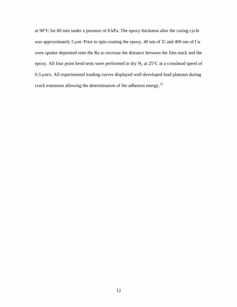
Examination of thicker films by XRD showed that they are polycrystalline
ruthenium films. Figure 6 shows X-ray diffraction spectra measured from a 180-nm-
thick film deposited at 300°C. These films were randomly oriented. Annealing these
films at 500 °C and 750 °C in N2 at 15 Torr for 1 min did not cause the XRD spectrum to
change significantly, indicating that Ru recrystallization is negligible at these
temperatures.
The TEM image of a 30-nm-thick film on a Si3N4 membrane shows that the grain
size is about 5 to 20 nm (Figure 7). Because the film was deposited on both sides of the
6

membrane, some Moire patterns appear due to interference between grains in the two
films. These investigations lead to the conclusions that the Ru films are smooth,
nanocrystalline, and structurally stable.
A test of film continuity was made by depositing a 2-nm-thick Ru film on a 3 nm
thick freshly deposited tungsten nitride film on a 30 nm Si3N4 membrane. The TEM of
this structure in Figure 8 shows that the Ru grains on WN are much smaller and more
densely spaced than on Si3N4 (Figure 7). This sample was then submerged in a WN
etching solution [H2O2:NH3: H2O (1:1:5)] for 10 mins. In a separate experiment, this
solution was found not to etch Ru films. Energy dispersive X-ray spectroscopy (EDX)
analysis revealed the presence of Ru and W both before and after submersion in the
etchant. In contrast, a WN film that was not capped with a 2 nm Ru layer was completely
etched in the same solution within seconds. These results show that there are no gaps or
pinholes in this very thin Ru film. TEM analysis of the Ru-capped film before and after
etching showed no difference in terms of the size or density of nuclei.
To extend on these results, the layers were intentionally pierced with holes and
then left in the etching solution for ∼12 hours to ensure complete dissolution of the WN
by undercutting from the edges of the holes. After etching, some fragments of the Ru
film settled back onto the substrate. Figure 9 shows a TEM image of one of these pieces
of Ru film that had been released from the substrate by dissolution of the WN. The Ru
film is clearly continuous, free of pin-holes and self-supporting. The existence of these
intact fragments is further proof of the continuity and uniformity of the 2-nm-thick Ru
films.
7

The in-plane resistivities of the Ru films on WN were measured with a 4-point
probe. A small correction was made for the parallel conduction through the WN. The Ru
resistivity increases with decreasing film thickness owing to several effects: grain
boundary scattering, electron-surface scattering, surface-roughness-induced scattering,
and impurity scattering. The curve in Figure 10 is calculated from a simple model that
includes only grain-boundary scattering,16
ρ/ρ0 = 1 + 1.5{R/(1-R)}(λ/g) (2)
where ρ0 is the bulk resistance of 7.1 μΩ-cm, λ is the electron mean free path (estimated
to be 10 nm), g is the average size of the grains (approximated as the film thickness), and
R ~ 0.58 is the grain-boundary-scattering coefficient (obtained by fitting the data in Fig.
10). It is remarkable that the data for Ru films produced by ALD follow this model down
to thicknesses of 2 nm. This agreement between measured conductivity and the model
suggests that the ruthenium film must be continuous and nearly uniformly covering the
WN surface. The agreement between the resistivity of the ALD Ru films and pure
sputtered Ru films shows that impurities in the ALD films do not have any significant
effect on their electrical resistance.
One of the challenges in multilevel metallization of the sub-90 nm generation
devices is the void-free filling of high aspect ratio contact holes. Non-conformal Ru films
can cause shoulders near the top of the holes, leading to void formation when the holes
are filled by Cu or W. The CVD and ALD Ru films were highly conformal inside holes
in Si with aspect ratios of 40:1. Figure 11 shows a scanning electron microscopy (SEM)
image of cleaved cross sections of ALD Ru films inside UV/ozone treated Si holes. The
film thickness at the top of the holes is found to be 50 nm, while the thickness at the
8

middle and bottom of the holes is 40 nm. This gives a step coverage of 80%. The
deviation away from ideal 100 % step coverage may be due to the partial self
decomposition of the precursor, or to insufficient exposure to the precursor.17
Ru adhesion energies are listed in Table I. The Ru/SiO2 interface can be
separated by Scotch tape. Four point bend tests for Ru/SiO2 give an adhesion energy of
less than 3 J m-2.18 In contrast, the Ru/WN/SiO2 stack passes the tape test and exhibits
strong adhesion. Four point bend tests indicate that the WN/SiO2 interface has an
adhesion energy of at least 17.6 ± 3.8 J/m2, where the location of the adhesive failure was
confirmed by XPS analysis of both interfaces exposed by the crack. It was not possible to
break the Ru/WN interface in the film stack under the same testing conditions.
Conclusions
We conclude that CVD and ALD of Ru on WN can provide highly conformal,
continuous, and strongly adherent layers that are suitable for many applications. The
process does not require oxidizing conditions or plasmas, which can damage substrates.
The Ru films nucleate densely on freshly-deposited WN and are continuous and pin-hole-
free at thicknesses down to 2 nm. The polycrystalline films are substantially free of
impurities, and have resistivities matching those of pure sputtered Ru films.
Acknowledgments
We appreciate the help with the AFM imaging from Dr. Zhengwen Li and
Qiaobing Xu. Youbo Lin acknowledges support from SRC, contract 2005-KC-1292.010.
A portion of the work presented here was carried out at the Center for Nanoscale Systems
at Harvard University. This work was supported in part by the National Science
Foundation.
9

Experimental
Pulsed CVD of ruthenium was carried out by thermal decomposition of bis(N,N'-
di-tert-butylacetamidinato) ruthenium(II) dicarbonyl, Ru(tBu-Me-amd)2(CO)2 without
any other reactant or reducing agent. The detailed synthesis and characterization of the
precursor will be published separately.19 The compound is monomeric, with a distorted
octahedral structure. The vapor pressure of Ru(tBu-Me-amd)2(CO)2 is about 0.05 Torr at
130 °C, based on sublimation data. 10 grams of the Ru precursor were placed in a
stainless steel container with a volume of 130 cm3 and heated (typically to a temperature
of 130 oC) in an oven. Nitrogen carrier gas (2.5 x 10⁻⁴ moles) was admitted to the
headspace volume above the precursor, resulting in a gas mixture of 1 mol % Ru
precursor and 99 mol % N2 at a total pressure of about 6.4 mbar. Meanwhile, the
deposition chamber (a stainless steel tube with volume 386 cm3) in a tube furnace was
pumped down to a base pressure of about 0.05 mbar, and then an air-actuated valve
between the deposition chamber and the pump was closed, admitting a dose of 1.8 x 10⁻⁶
moles of Ru precursor to the deposition chamber. The coated area (including the
substrates, the substrate holder and the heated chamber walls) was 686 cm2, so the dose
was 0.26 nanomoles per square centimeter. The valve between the precursor source and
the deposition chamber was next opened for 2 seconds and then closed. After a period of
2 more seconds, the valve between the deposition chamber and the pump was opened for
25 seconds, and 5.6 x 10⁻⁴ moles of nitrogen purging gas was admitted to help sweep out
byproducts and any unreacted precursor vapor. The exposure of the Ru precursor to the
surfaces was 0.086 mbar-sec. This CVD dose was then repeated a specified number of
times.
10

ALD of ruthenium was carried out with the same equipment as was used for the
pulsed CVD of Ru. The doses of Ru precursor vapor were alternated with doses of
ammonia gas. The ammonia dose from a measured volume (22 cm3 at a pressure of 1.24
bar) flowed into the evacuated deposition region, where it was also confined for a time
period (typically 3 seconds) before purging. The dose of ammonia was 1.06 micromole
cm-2 and the exposure was 200 mbar-sec.
The substrates used had 300 nm of thermal oxide on Si (100). Before deposition,
the substrates were treated for 4 minutes with UV/ozone to remove organic contaminants.
ALD WN as a diffusion barrier and adhesion layer was deposited on the SiO2 substrates
at 380 °C using ALD with bis(tert-butylimido)bis(dimethylamido) tungsten(VI) and
ammonia gas as precursors.20 Typically, 10 cycles were used to make a WN layer about
2.5 nm thick.
Some Ru samples were annealed in a rapid thermal annealing (RTA) furnace at
500 °C and 750 °C for 1 min in a vacuum (14.7 Torr). The crystal orientation of the as-
deposited and annealed Ru films was evaluated by using a θ-2θ x-ray diffractometer
(XRD; Scintag. Inc., USA) with Cu Kα radiation generated at 40 kV and 30 mA. Film
resistivity was calculated from the sheet resistance measured with a four-point probe and
the film thickness. The film thickness was measured using 2 MeV He+ Rutherford
backscattering spectroscopy (RBS). TEM pictures were taken with Ru/WN stacks on
amorphous SiO2 or Si3N4 membrane grids supplied by SPI Supplies.
Adhesion measurements were performed using the four point bend technique.
Test specimens were prepared by bonding Si wafers to the substrates with the
Ru/WN/SiO2 film stack using a spin-on epoxy (EPOTEK353ND). The epoxy was cured
11
at 90°C for 60 min under a pressure of 8 kPa. The epoxy thickness after the curing cycle
was approximately 5 μm. Prior to spin-coating the epoxy, 40 nm of Ti and 400 nm of Cu
were sputter deposited onto the Ru to increase the distance between the film stack and the
epoxy. All four point bend tests were performed in dry N2 at 25°C at a crosshead speed of
0.3 μm/s. All experimental loading curves displayed well-developed load plateaus during
crack extension allowing the determination of the adhesion energy.21
12

Table I. Adhesion measurements for ALD and CVD multilayer structures. Adhesion
energy was evaluated by four-point bend tests.
Adhesion energy
Structure Scotch tape test (J/m2)
Ru/SiO2 Failed <3
WN/SiO2 Passed 17.6 ± 3.8 J/m2
Ru/WN/SiO2 Passed > 17.6 J/m2
13

Figure Captions
Figure 1. (a) The chemical formula of Ru precursor bis(N,N’-di-tert-
butylacetamidinato)ruthenium(II) dicarbonyl, Ru(tBu-Me-amd)2(CO)2.
(b) its molecular structure by X-ray crystallography (hydrogen atoms not shown).
Figure 2. The Ru growth rate with NH3 (ALD) or without NH3 (pulsed CVD) at different
temperatures.
Figure 3. Pulsed CVD growth rate of Ru without using NH3 (squares) and ALD growth
rate (circles) as a function of temperature.
Figure 4. SIMS depth profiles of a ruthenium film 20 nm thick deposited on thermal SiO2
at 300 oC; the observed carbon and oxygen counts/second have been converted to
concentrations; the ruthenium curve represents the signal in counts per second because a
sensitivity factor is not known for Ru.
Figure 5. AFM image of a 87 nm ruthenium film grown at 300 ºC. (a) 2-D view; (b) 3-D
view.
Figure 6. XRD patterns obtained from a Ru film as deposited and after annealing.
Figure 7. TEM images of a Ru film (30 nm) deposited over Si3N4 membrane (30nm).
14

Figure 8. TEM of a Ru film grown on freshly deposited tungsten nitride on a Si3N4 TEM
membrane.
Figure 9. TEM image of a fragment of a Ru film of after etching of WN in a pierced film
of Ru(2nm)/WN(3nm)/SiO2 deposited on Si3N4 membrane (30 nm). The darker areas are
regions where the film folded over on itself.
Figure 10. The resistivity of Ru thin films as a function of Ru film thickness on WN
substrates. Black squares are data from this study, gray dots are data from sputtered Ru.
Figure 11. Ru films deposited inside the high aspect ratio (40:1) trench structure showing
excellent conformality of pulsed CVD process. The white bar on the bottom of each
image represents 200 nm.
15

References
1 a) C. S. Hwang, Mater. Sci. Eng. B 56, 178 (1998); b) M. Nayak, S. Ezhilvalavan, T. Y.
Tseng, in Handbook of Thin Film Materials, H. S. Nalwa, Ed., Academic Press, San
Diego, CA, p.121 (2001).
2 M. Tapajna, P. Pisecny, R. Luptak, K. Husekova, K. Froehlich, L. Harmatha, J. C.
Hooker, F. Roozeboom, J. Jergel, Materials Science in Semiconductor Processing 7, 271
(2004).
3 T. Seidel, A. Londergan, J. Winkler, X. Liu, S. Ramanathan, Solid State Technol. 46, 67
(2003).
4 I. Goswami, R. Laxman, Semiconductor International 27, 49 (2004).
5 T. Takenaga, T. Kuroiwa, T. Furukawa, M. Taki, K. Yoshiara, Y. Tokuda, Jpn. J. Appl.
Phys. 99, 08C911 (2006).
6 B. J. Mun and S. Hak, US Patent 7,125,655.
7 A. Koeckritz, M. Sebek, A. Dittmar, J. Radnik, A. Brueckner, U. Bentrup, M.-M. Pohl,
H. Hugl, W. Maegerlein, J. Molecular Catalysis A: Chemical 246, 85 (2006).
8 M. L. Green, M. E. Gross, L. E. Papa, K. J. Schnoes, and D. Brasen, J. Electrochem.
Soc. 132, 2677 (1985); T. Aoyama and K. Eguchi, Jpn. J. Appl. Phys. 38, L1134 (1999).
9 J. C. Viguié and J. Spitz, J. Electrochem. Soc. 122, 585 (1975); J. Vetrone, C. M. Foster,
G.-R. Bai, A. Wang, J. Patel, and X. Wu, J. Mater. Res. 13, 2281 (1998); J.-H. Lee, J.-Y.
Kim, S.-W. Rhee, D. Y. Yang, D.-H. Kim, C.-H. Yang, Y.-K. Han, and C.-J. Hwang, J.
Vac. Sci. Technol. A 18, 2400 (2000).
10 E. P. Boyd, D. R. Ketchum, H. Deng, and S. G. Shore, Chem. Mater. 9, 1154 (1997); Y.
Senzaki, W. L. Gladfelter, and F. B. McCormick, Chem. Mater. 5, 1715 (1993); Y.-H.
16

Lai, Y.-L. Chen, Y. Chi, C.-S. Liu, A. J. Carty, S.-M. Peng, and G.-H. Lee, J. Mater. Res.
13, 1999 (2003).
11 T. Aaltonen, P. Alén, M. Ritala, and M. Leskelä, Chem. Vap. Deposition 9, 45 (2003).
12 O.-K. Kwon, J.-H. Kim, H.-S. Park, and S.-W. Kang, J. Electrochem. Soc. 151, G109
(2004 ).
13 T. Aaltonen, M. Ritala, K. Arstila, J. Keinonen, and M. Leskelä, Chem. Vap.
Deposition 10, 215 (2004).
14 Y.-S. Min, E. J. Bae, K. S. Jeong, Y. J. Cho, J.-H. Lee, W. B. Choi, and G.-S. Park,
Adv. Mater. 15, 1019 (2003).
15 O.-K. Kwon, S.-H. Kwon, H.-S. Park and S.-W. Kang, Electrochem. Solid State Lett. 7,
C46 (2004)
16 S. M. Rossnagel and T. S. Kuan, J. Vac. Sci. Technol. B 22, 240 (2004).
17 R. G. Gordon, D. Hausmann, E. Kim and J. Shepard, Chem. Vap. Deposition 9, 73
(2003).
18 R. Wang, H. Chung,X. Tang, J. Y. Wang, W. D. Wang, Y. Tanaka, J. M. Yu and P.
Gopalraja, US Patent Application US2007/0059502.
19 Huazhi Li, Titta Aaltonen, Zhengwen Li, Booyong S. Lim, and Roy G. Gordon, to be
published.
20 J. S. Becker, S. Suh and R. G. Gordon, Chem. Mater. 15, 2969 (2003).
21 J. J. Vlassak, Y. Lin and T.Y. Tsui, Materials Science and Engineering A 391, 159
(2005).
17

(a) (b)
Figure 1. (a) The chemical formula of Ru precursor bis(N,N’-di-tert-
butylacetamidinato)ruthenium(II) dicarbonyl, Ru(tBu-Me-amd)2(CO)2.
(b) its molecular structure by X-ray crystallography (hydrogen atoms not shown).

Figure 2. The Ru growth rate with NH3 (ALD) or without NH3 (pulsed CVD) at different
temperatures.

0.0017 0.0018 0.0019 0.0020 0.00210.001
0.002
0.007
0.018
0.050
0.135
0.368
1.000
Gro
wth
rat
e
1/T (K-1)
With NH3
Without NH3
Figure 3. Pulsed CVD growth rate of Ru without using NH3 (squares) and ALD growth
rate (circles) as a function of temperature.

1E+16
1E+17
1E+18
1E+19
1E+20
1E+21
1E+22
1E+23
0 50 100 150 200 250 300
Depth (angstroms)
CO
NC
ENTR
ATI
ON
(ato
ms/
cc)
1E+00
1E+01
1E+02
1E+03
1E+04
1E+05
1E+06
1E+07
Cou
nts
Per S
econ
d
C
16O/18O
Ru
Figure 4. SIMS depth profiles of a ruthenium film 20 nm thick deposited on thermal SiO2
at 300 oC; the observed carbon and oxygen counts/second have been converted to
concentrations; the ruthenium curve represents the signal in counts per second because a
sensitivity factor is not known for Ru.

(a) (b)
Figure 5. AFM image of an 87 nm ruthenium film grown at 300 ºC. (a) 2-D view; (b) 3-D
view.
Figure 6. XRD patterns obtained from a Ru film as deposited and after annealing.

Figure 7. TEM images of a Ru film (30 nm) deposited over Si3N4 membrane (30nm).

Figure 8. TEM of a Ru film grown on freshly deposited tungsten nitride on a Si3N4 TEM
membrane.

Figure 9. TEM image of a fragment of a Ru film of after etching of WN in a pierced film
of Ru(2nm)/WN(3nm)/SiO2 deposited on Si3N4 membrane (30 nm). The darker areas are
regions where the film folded over on itself.

Figure 10. The resistivity of Ru thin films as a function of Ru film thickness on WN
substrates. Black squares are data from this study, gray dots are data from sputtered Ru.

Figure 11. Ru films deposited inside the high aspect ratio (40:1) trench structure showing
excellent conformality of pulsed CVD process. The white bar on the bottom of each
image represents 200 nm.