Embed Size (px)
Citation preview

Vanadium Oxide Microparticles Encapsulated in Graphitic Carbon
Master Thesis
Asem Ampoumogli Surfaces And Thin Films Group
Nanoscience Topmaster
Rijksuniversiteit Groningen Supervisor: Prof. Dr. P. Rudolf Referee: Prof. Dr. Ir. A.J. Minnaard
Groningen 2007

Asem Ampoumogli – Surfaces and thin Films Group
- 2 -
Vanadium Oxide Microparticles
Encapsulated in Graphitic Carbon
Asem Ampoumogli -
Surfaces And Thin Films Group -
Topmaster Nanoscience

Asem Ampoumogli – Surfaces and thin Films Group
- 3 -
Chapter 1 Introduction.................................................................................................- 5 -
1.1 Vanadium and Vanadium Oxides ...................................................................- 5 -
1.1.1 Catalytic Properties.................................................................................- 8 -
1.2 The Mott-Hubbard transition ..........................................................................- 9 -
Chapter 2 Synthesis ...................................................................................................- 11 -
2.1 Introduction...................................................................................................- 11 -
2.2 Chemical Vapour Deposition........................................................................- 11 -
2.2.1 Synthesis Procedure ..............................................................................- 13 -
Chapter 3 Characterization Techniques.....................................................................- 17 -
3.1 Techniques ....................................................................................................- 17 -
3.2 Powder X-Ray Diffraction............................................................................- 17 -
3.2.1 Theory of XRD .....................................................................................- 18 -
3.2.2 Results of XRD.....................................................................................- 18 -
3.3 Electron Microscopies ..................................................................................- 23 -
3.3.1 Transmission Electron Microscopy ......................................................- 23 -
3.3.2 Energy Dispersive X-ray Analysis........................................................- 24 -
3.3.3 Results of Transmission Electron Microscopy .....................................- 25 -
3.3.4 Scanning Electron Microscopy (SEM) .................................................- 27 -
3.3.4.1 Results...............................................................................................- 28 -
3.3.5 Electron Backscattered Diffraction.......................................................- 31 -
3.4 Melt Characterization....................................................................................- 33 -
3.5 Raman spectroscopy .....................................................................................- 37 -
3.5.1 Theory of Raman Spectroscopy............................................................- 38 -
3.5.2 Results...................................................................................................- 38 -
Chapter 4 Catalytic Properties...................................................................................- 41 -
4.1 Catalytic Measurements................................................................................- 41 -
4.1.1 Thin Layer Chromatography.................................................................- 44 -
4.1.2 1H and 13C NMR ...................................................................................- 45 -
4.1.2.1 Results...............................................................................................- 46 -
4.2 The Catalyst After Application.....................................................................- 47 -
Chapter 5 Synopsis ....................................................................................................- 50 -

Asem Ampoumogli – Surfaces and thin Films Group
- 4 -
5.1 Conclusions...................................................................................................- 50 -
Chapter 6 Bibliography .............................................................................................- 51 -
Chapter 7 Acknowledgements...................................................................................- 56 -

Asem Ampoumogli – Surfaces and thin Films Group
- 5 -
Chapter 1 Introduction
1.1 Vanadium and Vanadium Oxides Vanadium was discovered in Mexico in 1801 by the Spanish mineralogist A.M. del Rio who claimed it was present in a brownish lead mineral and named the element erythronium. However, it was falsely declared to be impure chromium and not a new element [1]. In 1830 the Swedish chemist N.G. Sefström rediscovered the element and named it vanadium after “Vanadis”, the old Norse name for the Scandinavian fertility goddess Freyja because of its beautiful multicoloured compounds.
Vanadium is one of the most abundant metals in the earth’s crust. Major suppliers of it are Australia, China, Russia and South Africa. The current annual production is about 38,000 tonnes. The primary uses of vanadium are metallurgical and 80% of the global production is used as a steel additive as it makes steel shock- and vibration-resistant. Vanadium is a powerful alloying agent. It is added to steel in the form of either ferrovanadium (vanadium-iron alloy) or vanadium carbide. It is also a major alloying element in high-strength titanium alloys. Other uses are in electronics and finally vanadium salts are well known for the brilliant orange and blue colors in ceramics or in dyes for textiles and leather [1].
Vanadium oxides present a wide range of structures. The principal oxides of vanadium occur as single valency oxides in the oxidation states from V2+ to V5+, i.e. in the forms of VO (V2+, rocksalt structure), V2O3 (V3+, corundum structure with rhombohedral symmetry), VO2 (V4+, rutile structure) and V2O5 (V5+, layered orthorhombic structure), each of which is stable over a certain composition range [2]. However, the vanadium-oxygen phase diagram includes mixed valency oxides containing two oxidation states such as V6O13, with V4+ and V5+ and a series of oxides between VO2 and V2O3 (e.g. V8O15, V6O11 etc.) which contain V4+ and V3+ species. These mixed valency oxides are formed by introducing oxygen vacancy defects into the respective
Oxide Oxidation state
Crystal structure
TC (ºK)
Magnetic structure (T<TC)
Optical bandgap
V2O5 V5+ (3d0) Orthorhombic (layered) Diamagnetic ~2eV
VO2 V4+ (3d1) Rutile (T>TC), monoclinic 340 Diamagnetic
Metallic (T>TC), 0.7
eV
V2O3 V3+ (3d2) Corundum
(T>TC), monoclinic
168 Antiferromagnetic (TN=168ºK)
Metallic (T>TC), 0.2
eV VOX V2+ (3d3) Cubic (rocksalt) Magnetic Function of x
Table 1-1: Basic properties of vanadium oxides (from [3])

Asem Ampoumogli – Surfaces and thin Films Group
- 6 -
Figure 1-1: Corundum structure of V2O3 (from [4]). The black spots denote V ions and the grey spots denote O ions. V2O3 occurs in the corundum structure above 168K and in a monoclinic phase below
168K.
higher oxides [3]. Table 1-1 demonstrates the basic properties of the main vanadium oxides.
V2O3 shows the corundum structure (Figure 1-1) in which the V ions are arranged in V-V pairs along the c axis and form a honeycomb lattice in the ab plane. The oxidation state of V ions is V3+ with 3d2 configuration. Each V ion is surrounded by an octahedron of O atoms [5].
The technological applications include electrical and optical switching devices, critical temperature sensors, light detectors and write-erase media [3]. In V2O3, with the addition of a few percent Cr, Al, Ti or a rare earth, a discontinuity in resistivity occurs in the range of -100°C up to 200°C, the so-called Mott transition. These properties allow it to be used in many different devices such as temperature sensors and current regulation [6]. The abrupt variation in the optical properties of V2O3 during its phase transition makes it suitable for electro-optical applications: It may be used as a memory medium for writing and storing optical information, it may be utilized for controlled mirrors with variable refraction index or as an infrared detector [7]. V2O3 powder is used in conductive polymer composites [8].
Most notably, vanadium oxides are used in heterogeneous catalysis [3]. This is the dominant non-metallurgical use of vanadium and represents about 5% of the annual production. Actually, vanadium is the most important metal used in metal oxide catalysis, as can be seen in Figure 1-2. This figure summarizes the number of papers (expressed as a percentage of the total number of papers) of several transition metals in the field of metal oxide catalysis, published between 1967-2000 which can be found in the open literature [1].
Most investigations on vanadium oxides are concerned with thin films [3] and this for numerous reasons: They provide model surfaces, which are important because the

Asem Ampoumogli – Surfaces and thin Films Group
- 7 -
surfaces of the bulk oxides are difficult to prepare. Moreover, such models on metallic substrates can be used to avoid charging problems of the single crystal oxides and thus allow the application of the many electron based surface science techniques [3]. Thin film vanadium oxide films are technologically interesting in their own right, with applications ranging from devices through sensors to protective coatings and catalysis. The nanostructures that arise can be quite novel with properties very different from the bulk oxides [3].
At present the preparation of (V1-xCrx)2O3 materials is primarily in the form of single crystals and micro-grain ceramics [9]. There are few studies of vanadium oxides in particle or powder form [9]. It is known that the particle size distribution and morphology of powder materials have a potential influence on the properties of the materials and functional devices [10]. Methods that have been used to produce micropowder include [10]: H2-O2 flame fusion of V2O3 at 2000°C, reduction in H2 flow of the product of the evaporative decomposition of V2O5 and reduction of sol-gel synthesized V2O5 powder. For the production of nanoparticles , three methods have been used [10]: Laser-induced vapour-phase reaction, reductive pyrolysis of ammonium oxovanadium(IV) carbonate hydroxide (NH4)2[(VO)6(CO3)4(OH)9]·10H2O in H2 flow and thermal decomposition of an appropriate oxalate.
Fabrication of low-dimensional structures of the vanadium oxides is difficult and one of the major problems encountered during the synthesis and preparation of thin films, nanostructures and nanocrystals is tuning the process parameters towards controlled growth and desired properties [2]. This is because the range in processing parameters over which these oxides form a stable single-phase material is relatively small. In particular, structural transitions between oxides in the V2O5-V2O3 system are complex and many intermediate oxides exist within this compositional range [2]. However, low-dimensional structures of V2O3 often exhibit novel and interesting properties and phenomena dissimilar to those of the bulk oxide. The spatial confinement at reduced dimensions is responsible for structures that, compared to their bulk equivalents, display modified chemical bonding and enhanced chemical activity [2].
Figure 1-2: The importance of vanadium in catalysis by supported metal oxides (from [1]).
The percentages are based on an extensive open literature search between 1967-2000.

Asem Ampoumogli – Surfaces and thin Films Group
- 8 -
Chemical vapour deposition (CVD, the method used in this research work) is being increasingly used for the synthesis of VOx thin films [11] and there is one record of CVD being used to produce vanadium nitride powder [12] but other than this we have been unable to find instances of CVD being used to produce the particulate or powder form of vanadium oxides.
1.1.1 Catalytic Properties
Vanadium oxides are catalytically active compounds. Supported vanadium oxide catalysts possess outstanding redox properties and are primarily employed as selective oxidation catalysts [13]. Vanadium oxide is a key component in the preparation of catalysts for oxidation reactions. It is used either as a supported active phase or in combination with some other ions to form mixed oxides in order to obtain a system with modified and enhanced oxo-reductive properties [14].
Most catalysts based on vanadium oxide consist of a vanadium oxide phase deposited on the surface of an oxide support, such as SiO2, Al2O3, TiO2 and ZrO2. Supporting a metal oxide on the surface of another oxide was initially proposed to improve the catalytic activity of the active metal oxide phase due to a gain in surface area and mechanical strength [1].
Examples of the reactions vanadium oxides catalyze are [1]: Selective oxidation of alkanes and alkenes, selective catalytic reduction of NOx with NH3, oxidation of SO2, polymerization of olefins and decomposition of isopropylalcohol.
V2O3 specifically, is an effective catalyst for the Water-Gas Shift (WGS) reaction, a technologically important reaction in which water and carbon monoxide react towards hydrogen and carbon dioxide, while V2O5 is inactive in this reaction [14].
In view of the importance of vanadium oxides in different applications, the fabrication of these materials in nanostructured form is a particularly attractive goal. When the dimensionality of oxide materials is reduced new properties may appear [15]. Nanometric oxide structures in the form of ultrathin layers, linear elements, quantum dots and three dimensional clusters are significant as passive and active elements in different areas of nanotechnology [15]. For example nanocomposites of V2O5 in combination with conducting polymers have been designed as cathode materials for rechargeable Li+ batteries [16]. Vanadium oxide nanotubes and nanowires are of particular interest in electrochemistry and catalysis [17]. In all these areas the controlled fabrication of nanostructured oxide phases is required [15].
In this study we synthesized pure and Cr-doped vanadium micro-particles encapsulated in carbon layers produced by the decomposition of acetylene gas. The average diameter of the particles produced is close to 100μm as can be seen from SEM images (section 3.3.4.1). The project was initially based on a project by L. Jancovic, D. Gournis and P. Rudolf [18]. In that project a similar Chemical Vapour Deposition method was used to grow Sn-filled nanotubes starting from a powder of tin dioxide.
By the carbon confinement we hoped to protect the oxide micro-phase V2O3 against oxidation while it was stored, as well as while it was being used as a catalyst. Encapsulated catalysts are not unknown, in fact an example of encapsulated catalysts are the EnCat catalysts produced by Reaxa [19], a product range of polyurea-encapsulated Pt/Pd/Os/Co particles and complexes. The concept aims to minimize the contamination of

Asem Ampoumogli – Surfaces and thin Films Group
- 9 -
the reaction product and the reaction vessel by the metal catalyst, and to make it easier to recover the catalyst.
Additionally, we hoped to examine the influence of the micro-dimensions on the Mott-Hubbard transition (explained in short in section 1.2) as this is such a technologically important property [6].
1.2 The Mott-Hubbard transition The metal-insulator transitions such as the one V2O3 demonstrates are of great
experimental and theoretical interest and are greatly challenging [5] to physicists attempting to explain them. The successful theory of a phase transition must not only identify the transition mechanism but must also determine the physical properties of the phases involved.
The basic distinction between metals and insulators was based on the filling of their electronic bands at zero temperature [5]. For insulators, the highest filled band is completely filled, for metals it is partially filled. This remained a successful model until de Boer and Verwey reported in 1937 that many transition metal oxides with a partially filled d-band were poor conductors and indeed often insulators [20]. A typical example of this is NiO which should be a metal but is actually an insulator.
V2O3 undergoes a metal-insulator transition as a function of temperature, pressure and doping by other transition metals. The literature on doped and undoped V2O3 is vast ( > 500 papers by the end of the 90’s) [5]. The particular fascination with V2O3 is not unjustified because of the richness of the parameters that are related to the phase transition [21]. V2O3 is the only known example among transition-metal oxides to show a transition from a paramagnetic metal phase to a paramagnetic insulating phase [22].
The phase diagram of Cr-doped V2O3 (Figure 1-3) includes areas where the material is a paramagnetic metal (PM), a paramagnetic insulator (PI) or an antiferromagnetic insulator (AFI).
The first experimental observation was made in 1946 [21] in V2O3 by lowering the temperature below ~160K. Such materials are considered strongly correlated metals and the one-electron approach (the electron-gas model of metals) fails when one tries to predict their properties.
Mott proposed in 1952 [23] a theory in order to explain such discrepancies and showed that as the distance between the atoms in a lattice was increased, it would be possible for a metal to transform into an insulator, perhaps simultaneously with the onset of magnetic order. Hubbard produced [24] a simple many-body Hamiltonian with a meaningful description of two opposite tendencies: the kinetic energy tries to delocalize the electrons into itinerant (Bloch) states, leading to metallic behaviour, while the electron-electron interaction tries to localize the electrons, leading to a Mott insulator. This correlation-driven metal-insulator transition is refered to as the Mott transition (or Mott-Hubbard transition) since the idea was first introduced by Mott.
In this strongly correlated material two sub-bands arise: one for electrons and one for holes. The difference from a usual semiconductor is that in the Mott-Hubbard insulator the gap is an electronic phenomenon which depends on the electron density and originates from the repulsive interaction between carriers and not from the lattice periodicity as in the conventional semiconductors such as silicon [25].

Asem Ampoumogli – Surfaces and thin Films Group
- 10 -
Figure 1-3: A schematic diagram for the Cr-doped V2O3 system phases (from [26]). Shaded areas
indicate regions of hysteresis. For Cr concentrations below 0.5 at% the transition from PM to PM` is broad and continuous. For concentrations greater thatn 1.8% the transition is continuous. The
authors deduce the existence of two critical points.
When we originally planned the experiment we hoped we might be able to examine how the encasing of the microparticles would alter the expected transition and this is the reason for synthesizing the Cr-doped compounds instead of a pure carbon encased compound. Later however, our focus was turned to the catalytic aspects of the system alone.

Asem Ampoumogli – Surfaces and thin Films Group
- 11 -
Chapter 2 Synthesis
2.1 Introduction To produce the carbon-encased vanadium oxide nanoparticles we used Chemical
Vapour Deposition (CVD). This is one of the most commonly used methods [27] to synthesize carbon nanotubes, the others being arc-discharge and laser-ablation.
In short, the arc-discharge method is the one by which the first CNT’s were synthesized and identified. Two graphite electrodes are brought in contact in an inert gas atmosphere; applying a DC-voltage discharge between the electrodes causes carbon to evaporate from the anode and be deposited on the cathode as soot in the form of CNT’s and other carbon particles.
The laser-ablation method started to be used in the synthesis of CNT’s in 1996, after Smalley’s group developed it to create fullerenes [4]. In this method, the high energy density of a laser is used to vaporize a carbon target. The produced SWNT’s are conveyed by high-temperature Ar gas to a cold finger collector. The method produces SWNT’s of high crystallinity, purity and controlled diameter.
In contrast to these two processes which are considered high- temperature (>3000°C) and short- time (μ sec-msec) techniques, CVD is a low-temperature (<1400°C), long-time (min-hrs) technique. In short, during this process a hydrocarbon vapour is thermally decomposed over a catalyst and the CNT’s are deposited in situ. This is a low cost and simple technique to produce CNT’s.
2.2 Chemical Vapour Deposition Chemical Vapour Deposition is one of the most commonplace methods used in the
synthesis of CNT’s because it is highly versatile, simple and allows for better control of the growth parmeters [27]. It has been used for the production of carbon fibers and filaments since 1959. Endo et al. used CVD to grow CNT’s in 1993 [28] by the pyrolysis of benzene, to be followed by many others who varied the feedstock gas, the temperature and the catalyst [27]. SWNT’s were first created by Dai et al. [29] in 1996, using CO as a hydrocarbon source and Mo as a catalyst. Most known forms of carbon nanotubes (SWNT, MWNT, spiral) may be produced, in practically any arrangement, i.e. powder, films (aligned or not), in a forest arrangement or in any patterned form and even stand-alone tubes to serve as very sharp, robust and flexible tips for atomic force microscope probes.

Asem Ampoumogli – Surfaces and thin Films Group
- 12 -
Figure 2-1: A scheme of the CVD setup we used.
Figure 2-1 shows a scheme of the setup we used. In this process a hydrocarbon gas passes through a tube furnace, typically for 15-60 minutes, carried by a non-reacting gas (in this case argon). The catalyst is placed in this furnace, usually on the support that we desire to have the nanotubes.
The catalyst material may be solid, liquid or a gas itself. The hydrocarbon gas is decomposed over the catalyst because of the high temperature, the nanotubes are produced in situ and are collected after the system has been cooled to room temperature. It is assumed that the catalytically decomposed species coming from the feedstock gas are dissolved in the catalyst particles [27]. After the latter are supersaturated, the carbon precipitates out of the particle in the form of a fullerene dome which will extend to form a nanotube. Transition metals (Fe, Co, Ni) are the most commonly used catalysts for CNT growth. The phase diagram of carbon and these metals suggests finite solubility of carbon in these transition metals at high temperatures. This is thought to lead to the growth of nanotubes via the mechanism described above [27].
At the exit of the tube furnace there is a bubbler filled with water. The bubbles produced by the gas flow serve as an indication of the flow rate.
The three main parameters for nanotube growth in CVD are the hydrocarbon gas type, the catalyst and the temperature. Although the effects of the synthesis conditions on the reaction mechanisms are not always known with certainty, a few rules-of-the-thumb regarding CVD are [27]:
• Higher temperatures (900ºC-1200ºC) favour SWNT growth whereas lower
temperatures (600ºC-900ºC) will produce MWNT.

Asem Ampoumogli – Surfaces and thin Films Group
- 13 -
• In the case of a catalyst in the form of particles, the rule is that nanometer size particles will produce SWNT, while MWNT will be grown when the particles have diameters of a few tens of nanometers.
• SWNT’s can only be grown using selected gases (e.g. CO, CH4) that have a reasonable stability in the temperature range of 900ºC-1200ºC. Precursors which can efficiently produce MWNT’s (like acetylene or benzene) are unstable at higher temperatures and lead to the deposition of large amounts of carbonaceous compounds other than CNTs.
According to these rules we would expect our experiment to produce MWNT.
2.2.1 Synthesis Procedure
The Cr-doped V2O3 system is usually written in the literature as (V1-xCrx)2O3 and doping is given in terms of x [5], [30], [31], [32], where x is practically always in the range of 0.001 ≤ x ≤ 0.1.
Based on the existing literature (see section 1.2) we decided to synthesize seven samples, six doped and one undoped. All samples (except for the undoped one) are part of the (V1-xCrx)2O3 system, with 0.01 < x < 0.1 as shown in Table 2-1 where the nominal composition is reported.
Figure 2-2: A photograph of the CVD setup used in the synthesis. A detail of the tube furnace is shown as an inset.

Asem Ampoumogli – Surfaces and thin Films Group
- 14 -
Sample No Sample code x %wt of Cr %at of Cr
1 TAT1096 0.01 0.69 % 0.4 2 TAT1097 0.02 1.387 % 0.8 3 TAT1098 0.03 2.079 % 1.2 4 TAT1099 0.04 2.772 % 1.6 5 TAT1100 0.05 3.464 % 2 6 TAT1101 0.1 6.924 % 4 7 TAT1102 0 (undoped) - -
Table 2-1: The samples in the series (V1-xCrx)2O3 synthesized in this study. The values of the Cr
doping percentages are the theoretically expected ones for each sample. The two starting compounds were vanadium pentoxide (V2O5) and chromic anhydride (CrO3), a brilliant red crystalline substance, regarded as the anhydride of chromic acid (H2CrO4). Both compounds being of analytical purity (Aldrich). All the quantities we used have been calculated with the assumption that all quantities will be used to the fullest and that there would be enough time for the mixture to become homogeneous. The furnace used was the Carbolite MTF 10/25/130. The flowmeter was the Omega FMA-A2402-SS.
These solid powder samples were weighed and then mixed in a mortar by grinding with a pestle. Vanadium pentoxide is a light orange powder, while chromium trioxide is a dark orange-to-red powder, thus a homogeneous colour was a good indication that the compounds had been mixed properly.
The setup we used is shown schematically in Figure 2-1. In Figure 2-2 is a photograph of the same CVD setup and a detail of the setup, the tube furnace is shown as an inset. During the CVD process two things would happen simultaneously: Firstly, the compounds (V2O5 and CrO3) would melt and mix into the desired compound i.e. Cr-doped V2O3. Secondly, as soon as the acetylene gas was allowed into the system, the graphite layers would form around the particles.
Figure 2-3: A photo of the quartz boat before being placed in the furnace. The reaction mixture (V2O5+CrO3) can be seen in the boat.

Asem Ampoumogli – Surfaces and thin Films Group
- 15 -
100 mgr of each of the seven mixtures are placed in a custom-made quartz boat (shown in
Figure 2-3). The boat is carefully placed in the tube of the furnace, where the center of the furnace’s heating zone is, and the gas pipes and flanges are connected and tightened. The argon gas feed is then opened and argon is allowed through the furnace for ten minutes to remove other gases from the sample and the CVD system. After this, the furnace temperature program is started. The target temperature for the synthesis is 700°C and the furnace arrived at this temperature in about 15-18 minutes. After the target temperature is reached, the system is allowed to stay at that temperature for 20 additional minutes to make certain that the temperature across the furnace’s heating zone and the entire sample is even and stable. At this point the acetylene gas valve is opened and gas is let to run for 60 minutes. The acetylene flow is controled by a flowmeter. The total gas flow through the system is 100 cm3/sec, 10 cm3/sec of acetylene and 90 cm3/sec of argon carrier gas. A visual confirmation of the flow rate is given by the number of bubbles produced at the bubbler, at the end of the flow system. An optimum gas flow should produce about two bubbles per second (calibrated so that 90 cm3/sec are 120 bubbles/min).
Since acetylene is a flammable and explosive gas and CVD involves high tempertures, several safety precautions have to be observed during the CVD process and a check is required every five minutes of the process:
• The argon flow must not be reduced during the process as this could cause a buildup of acetylene in the system. This is monitored by the number of bubbles on the bubbler.
• Unreacted acetylene will form a yellow deposit on the tube at the exit of the furnace heating zone. If this was observed the experiment would have to be stopped.
• Accumulated acetylene will fog the gas in the bubbler. However, if the fogging becomes too evident this is also an indication of acetylene flow problems and the experiment has to be stopped.
Figure 2-4: The same sample after CVD has been completed.

Asem Ampoumogli – Surfaces and thin Films Group
- 16 -
Figure 2-4 shows what the sample looks like after CVD has been completed. The solid is collected and then stored in eppendorf tubes without any further treatment.

Asem Ampoumogli – Surfaces and thin Films Group
- 17 -
Chapter 3 Characterization Techniques
3.1 Techniques We used various techniques to analyze our samples and gain information about the
structure, morphology and chemical composition of our samples. Additionally, we tested the catalytic activity of the carbon-covered nanoparticles. Due to the tight time limits not all samples could be characterized by each technique. Table 3-1 shows a summary of the techniques applied to each sample.
sample XRD SEM SEM+EDX TEM Raman Catalytic tests
TAT1096 X X X TAT1097 X X TAT1098 X X TAT1099 X X X 2 X X X TAT1100 X X TAT1101 X X TAT1102 X X X X X
Pure V2O3 X
Table 3-1: The techniques applied to each sample.
3.2 Powder X-Ray Diffraction X-Ray Diffraction (XRD) probes the structure of crystalline samples. If the
crystalline structure of a substance is known then XRD can be used to identify the presence of this substance. Three of the samples were characterized by powder X-ray diffraction, namely TAT1102 (the undoped sample), TAT1096 (the least doped sample) and TAT1099 (the middle of the doped series).
The measurements were performed using a Bruker D8-Advance diffractometer in the Bragg-Brentano geometry. Starting angle was 2Θ=10.000°, end angle was 2Θ=100.000° with a step of 0.020°/sec. The X-rays were Cu Kα with an average wavelength λ of 1.54184 Å.
Asem Ampoumogli – Surfaces and thin Films Group
- 18 -
Figure 3-1: Bragg’s law of diffraction: An incoming wave is diffracted by the crystalline layers of the
material. The red dots denote atoms of the lattice.
3.2.1 Theory of XRD
X-rays will undergo diffraction when interacting with matter with interatomic distances comparable to the radiation’s wavelength (approximately 0.1 nm). The principle of measurement is based on Bragg’s law. Figure 3-1 illustrates the interference between waves scattering from two adjacent rows of atoms in a crystal. The scattered intensity will peak (constructive interference) when the path length difference of two beams scattered from different rows equals an integer multiple of the wavelength (n·λ).
The path difference between the rays scattering from the plane containing atom “A” and from the plane containing atom “B” is the distance CB+BD which is equal to 2·dsinΘ. The spectrum will then contain all peaks for which:
Θ= sin2dnλ (3-1)
Bragg’s law of diffraction allows us to calculate the spacing “d” when we measure the peaks of the scattered intensity. The spectra are given in 2-Theta angle (degrees) by convention.
3.2.2 Results of XRD
Figure 3-2 shows the powder XRD spectrum of the sample TAT1096, Figure 3-3 the spectrum of sample TAT1099 and Figure 3-4 the spectrum of sample TAT1102.

Asem Ampoumogli – Surfaces and thin Films Group
- 19 -
Figure 3-2: Powder XRD spectrum of TAT 1096. The 2-Theta scale is in degrees.

Asem Ampoumogli – Surfaces and thin Films Group
- 20 -
Figure 3-3: Powder XRD spectrum of TAT 1099. The 2-Theta scale is in degrees.

Asem Ampoumogli – Surfaces and thin Films Group
- 21 -
Figure 3-4: Powder XRD spectrum of TAT 1102. The 2-Theta scale is in degrees.

Asem Ampoumogli – Surfaces and thin Films Group
- 22 -
The following table summarizes the peaks measured for the three samples TAT1096 (the least doped), TAT1099 (the mid-doped) and TAT1102 (undoped). These are compared to the expected peaks for V2O3 from the XRD database [33]:
TAT1096 TAT1099 TAT1102 Pure V2O3 2Theta 2Theta 2Theta 2Theta Relative Intensity 24,276 24,320 24,360 24,314 71 31,867 32,143 32,235 32,987 100 36,267 36,243 36,296 36,231 80 38,657 38,707 38,625 38,514 6 41,258 41,245 41,303 41,216 36 44,132 44,138 44,180 44,099 7 49,877 49,858 49,901 49,811 34 54,042 54,040 54,036 53,923 85 58,466 58,486 58,366 7 63,213 63,211 63,239 63,115 24
64,779 65,236 65,262 65,284 65,195 31 70,949 70,977 70,871 70,688 14 76,961 77,058 77,124 76,916 6 78,508 78,488 78,357 4 82,300 82,114 9
82,422 82,341 82,575 2 86,425 86,267 4
89,636 89,597 89,600 89,515 12 93,369 93,396 93,207 9
93,490 93,693 3
Table 3-2: The powder XRD peaks for three samples. The pure compound peaks are from the ICDD Powder Diffraction Database [33].
From Table 3-2 it becomes obvious that the dominant phase in the samples we measured was in fact V2O3.
From the Electron BackScattered Diffraction analysis (Section 3.3.5) of sample TAT1102 (undoped sample) it appears the dominant phases (meaning they have the highest confidence index) in the material are V2O3 and V3O5. However, comparison of the 2-Theta values of V3O5 [34] indicate that the compound V3O5 is actually not part of our material at least for sample TAT1102. Similarly, comparing with the peaks for V2O5 (from the same database) indicates that this phase was also not part of our material.
There are no diffraction lines of CrVO4 (see section 3.4) in fact CrVO4 is known to form disordered and highly dispersed domains at low temperature, which show no diffraction lines [35] so, although grains of it may be present in our material, it would be undetected by powder XRD.

Asem Ampoumogli – Surfaces and thin Films Group
- 23 -
3.3 Electron Microscopies Microscopy is indispensable as a tool when characterizing a nanomaterial. In our case
we used microscopy to measure the size and shape of the vanadium particles and to measure the thickness of the graphite layers. We used Transmission Electron Microscopy (TEM) and Scanning Electron Microscopy (SEM) with two additional modules, EDX (Electron Dispersive X-ray Spectroscopy, also abbreviated to EDS) and OIM (Orientation Imaging Microscopy, also known as EBSD, Electron Back-Scattering Detection).
3.3.1 Transmission Electron Microscopy
The TEM technique is equivalent to the conventional optical microscope except that the radiation used is electrons instead of photons. The electrons typically employed in TEM have a de Broglie wavelength of 6 pm while for visible photons the value is about 600 nm. So with the electron microscope we can achieve a much higher resolution. A scheme of a transmission electron microscope is shown in Figure 3-5.
A ray of electrons is produced by transmission from a pin-shaped cathode heated by current. The electrons are accelerated through the vacuum electron column to an anode by the high voltage, typically between 50 and 150 kV. The higher the accelerating voltage, the more energetic the electrons are when they pass through the sample and the higher the resolution we can achieve. The maximum useful resolution that can be achieved is around 300,000 x.
The electron beam passes through a system of electromagnetic lenses .These are coils generating electromagnetic fields to manipulate the trajectory of the electrons.
Figure 3-5: Scheme of a transmission electron microscope (from
http://www.steve.gb.com/science/electron_microscopy.html)

Asem Ampoumogli – Surfaces and thin Films Group
- 24 -
The ray is first focused by a condenser coil and sent through the sample. Depending on the electron densities of the sample materials, the beam will be partially deflected and this creates the contrast of the final image. The greater the mass of the imaged atoms, the greater the deflection.
The electrons that are transmitted through the sample are collected by another system of lenses which enlarges the beam. This enlarged spot is made visible on a fluorescent screen or captured by a photographic plate. This is the so-called “dark field” imaging.
A crystalline material will also produce a diffraction pattern in addition to the contrast produced by the partial transmission. The intensity of diffraction will depend on the orientation of the sample crystal lattice relative to the electron beam. The electron microscope must then be equipped with an appropriate sample holder that will allow the operator to tilt the sample to obtain the diffraction conditions. In this case the TEM operates in the Bright Field conditions.
Information that can be obtained from a TEM includes: • The morphology, i.e. the shape and size of the particles making up the object. • The crystallographic information.
The TEM has a special mode of operation called High Resolution TEM (HRTEM). Consider a a very thin slice of crystal that has been tilted so that a low-index direction is exactly perpendicular to the electron beam. All lattice planes about parallel to the electron beam will be close enough to the Bragg position and will diffract the primary beam.The diffraction pattern is the Fourier transform of the periodic potential for the electrons in two dimensions. In the objective lens all diffracted beams and the primary beam are brought together again; their interference provides a back-transformation and leads to an enlarged picture of the periodic potential. This picture is magnified by the following electron-optical system and finally seen on the screen at magnifications of typically 106.
3.3.2 Energy Dispersive X-ray Analysis
Energy Dispersive X-ray Analysis (abbreviated to EDX or EDS) is a technique used for analyzing the elemental composition of a material. The EDX system works as a module of a SEM or a TEM as it uses the electron beam of those systems.
The principle of EDX measurement is the emission of characteristic X-rays from atoms (Figure 3-6). The electrons that bombard the sample occasionally create vacancies in the electron shells of the sample atoms. The left scheme shows an energetic electron (1) removing a K shell electron (2) by collision. This creates an excited state which may decay radiatively: On the right, electron (3) orbiting on the M shell drops on the K shell to fill the vacancy and in the process emits the difference in energy between shells K and M as an X-ray photon. The energy of this photon will depend on the relative energies of the shells which in turn depend on the nucleus content and are therefore characteristic of the atom that emits them. Thus by measuring these X-ray photons the identity and relative abundance of each element present can be established.

Asem Ampoumogli – Surfaces and thin Films Group
- 25 -
Figure 3-6: Emission of characteristic X-rays from an element after it has been excited by energetic electrons. Left: creation of a vacancy. Right: A higher-orbiting electron fills the vacancy and loses
energy in the form of an X-ray photon. The specific type of transition may also be identified e.g. the X-ray photon of an
electron moving down from the L shell to the K shell will be identified as a Kα peak. The photon from an electron dropping from the M shell to the K shell will be identified as a Kβ peak.
Inner-shell vacancies in elements with large atomic number correspond to large transition energies and usually decay by such radiative processes. Vacancies in elements with low atomic number or outer-shell vacancies with low transition energies decay primarily non-radiatively by Auger processes. In this case, the energy will be carried away by another electron which will escape the atom.
Both the SEM and the TEM that we used for measuring our samples were equipped with an EDX system.
3.3.3 Results of Transmission Electron Microscopy
The micrographs and spectra were recorded on a JEOL 2010F electron microscope of the Materials Science group of the Zernike institute for Advanced Materials.
To prepare a sample for the electron microscope we used a copper grid onto which a holey carbon grid was placed. We dispersed the vanadium particles by sonicating for less than 1 minute in iso-propanol. A drop is then placed on the copper grid and left to dry.
In Figure 3-7 we show the typical appearance of the sample TAT1099. We see needle shaped particles with a length of 50 micrometers. Smaller particles are also present as shown on the left of Figure 3-7.
On using the high-resolution mode of the TEM (HRTEM) we were able to discern the carbon layers that surround the particles. This is shown very clearly in Figure 3-8 which is a HRTEM micrograph of a particle of the sample TAT1099. On both pictures details from the same particle are shown. We see that the carbon layers are not very homogeneous in width and that significant variations can be observed. We also see that the carbon layers are not apparently aligned in a parallel fashion to each other but they present a disordered picture. For a characterization of the carbon layers see section 3.5 (Raman characterization).

Asem Ampoumogli – Surfaces and thin Films Group
- 26 -
Figure 3-7: Tem micrograph of two particles from the sample TAT1099..
Figure 3-8: HRTEM micrograph of the carbon layers surrounding a particle of the sample TAT1099.
The crystallinity of the particles becomes observable under HRTEM. This is can be seen in Figure 3-8 but it can also be very well observed in Figure 3-9. This is another HRTEM micrograph of another particle from the same sample (TAT1099). In this image grain boundaries separating different crystalline orientations within one vanadium oxide nanoparticle are clearly visible. To verify that these are indeed features of crystallinity we may perform diffraction through one of the particles. This is done in Figure 3-10. On the left of this image we see the edge of a needle-shaped particle of the sample TAT1099. On the right of this image there is a diffraction pattern from this same particle showing that it is in fact crystalline. In the literature these needle shaped structures are reported as the main form of V2O3 [36].

Asem Ampoumogli – Surfaces and thin Films Group
- 27 -
Figure 3-9: HRTEM migrograph of the bulk of a particle of the sample TAT1099
Figure 3-10: On the left: TEM micrograph of a particle of the sample TAT1099. On the right: diffraction pattern from this same particle.
3.3.4 Scanning Electron Microscopy (SEM)
The Scanning electron microscope is used for inspecting the morphology of the sample and is in this sense more akin to the optical microscope in that we see the surface of the sample. The magnification can be higher than 300,000x. A scheme of a SEM is shown in Figure 3-11. A beam of highly energetic (up to 100 KeV) electrons is produced in a vacuum column much like the one in a TEM instrument. The focal spot of this beam

Asem Ampoumogli – Surfaces and thin Films Group
- 28 -
Figure 3-11: Scheme of a scanning electron microscope (from http://www.steve.gb.com/science/electron_microscopy.html).
is from 0.4 up to 5 nm in size. This beam is rastered over an area of the sample to be
imaged. The bombarding electrons are energetic enough to dislodge one or more electrons
from the atoms of the sample. The vacancies are filled by electrons at higher shells in a process shown schematically in Figure 3-6. The energy released by electron (3) will allow another electron of this atom to escape the atom. This process of producing secondary electrons is the Auger decay. Secondary electrons can also be created by energy loss of the Auger electrons.
These secondary electrons are collected by a positively biased grid or detector and translated into an image of the sample topography.
The energy of the primary electrons determines the quantity of secondary electrons collected during inspection More energetic primary electrons will dislodge electrons deeper inside the material. The emission of secondary electrons from the specimen increases as the energy of the primary electron beam increases, until a certain limit. When this limit is reached, the collected secondary electrons imaged diminish as the energy of the primary beam is increased, because the secondary electrons are now produced deep below the surface of the specimen and are less likely to escape the sample bulk and be imaged.
Aside from the secondary electrons, some of the bombarding electrons will be backscattered from the sample. The yield of the backscattered electrons is proportional to the bombarded atoms’ atomic number.
3.3.4.1 Results

Asem Ampoumogli – Surfaces and thin Films Group
- 29 -
To prepare the SEM samples we dispersed a minute amount of the powder in iso-propanol by short sonication i.e. less than 1 minute. A drop of the dispersion was placed on a piece of silicon wafer and left to dry.
First we present an inspection of pure V2O3 as produced by “Alfa inorganics”. This should give an idea of what it was we expected from our particles. In Figure 3-12 we present a SEM micrograph of the pure V2O3 sample. On the left we see an overview of the material. We see that the material is made up of particles of different sizes. The average diameter of the particles is about 100 micrometers. They are approximately round in shape and present no sharp edges. On the right we present a detail from the surface of one particle from the same sample. The surface of this particle is quite rough. It points towards a disordered structure, since the flakes that we observe show no preferred direction.
Figure 3-12: SEM micrographs from a pure V2O3 sample. On the left: An overview of the material. On the right: A detail of the surface of one particle from this sample.
Figure 3-13: SEM micrographs of the TAT1102 sample. On the left we see an overview of the material and on the right a detail from the surface of one of the particles.

Asem Ampoumogli – Surfaces and thin Films Group
- 30 -
It is interesting to compare the pure V2O3 material with our undoped material TAT1102 which is pure V2O3 with carbon layers. This material is presented in Figure 3-13. On the left hand side we see an overview of the material. We see pebble-like particles that have no sharp edges, much like in the pure V2O3 material. The first observation that we can make is that this material has a broader size distribution. We can see particles that are significantly larger than in the pure material, as well as particles significantly smaller. On the right hand side of Figure 3-13 we have a surface detail of a particle of this material. The surface roughness is reduced compared to the pure material, as the platelets that seem to make up the surface are somewhat more aligned. The carbon layers cannot be observed at this length scale. The differences between the pure V2O3 material and sample TAT1102 are, to a degree, expected since different preparation routes were taken.
We will now go on to compare the Cr-doped samples to the pure V2O3 and the TAT1102 sample.
The general appearance of this sample is already quite different as can be seen from the overview of the sample TAT1096 which is presented in Figure 3-14. This overview image is very typical of the Cr-doped samples. We can see that there is no longer only one single type of particle but that there are now at least two. Some particles which are needle-shaped and some which have a more rounded appearance. The size distribution is also very broad in this sample. Most rounded particles have a diameter of about 100 microns, while the large dimension of the needle particles is at least twice that. The fact that we have now different kinds of particles is intriguing.
Figure 3-14: SEM overview of the sample TAT1096

Asem Ampoumogli – Surfaces and thin Films Group
- 31 -
An attempt to explain this is made in section 3.4 where it is argued that according to dynamics of a melt of two ceramic materials allowed to cool through successive equilibrium conditions, we should expect different kinds of particles to crystallize out of the melt at different temperatures, as the melt is cooling down. The types of particles that we will then observe will be a mixture of V2O3 particles, CrVO4 particles and intermediate particles made of lamellae consisting of alternating layers of CrVO4 and V2O3. Naturally, a few things are different from this ideal analysis. For example, we found during the EDX measurements that many particles had a significant contamination from Si. We assume that this comes from the Si boat on which we place the sample to put it through the CVD process.
Examining the surface of these two kinds of particles we find further differences. In Figure 3-15 we show the typical appearance of the surface of a needle-shaped particle from sample TAT1096. On the right we show a detail from the surface of one of the rounded particles from sample TAT1100. All needle-like and all round particles across all the doped samples look very similar and the choice of pictures was made on the basis of clarity.
What we immediately observe is that the needle-like particles are crystalline particles which present lamellae, however, the rounded particles present the self-same appearance as the particles of the pure V2O3 sample and on the same length scale. These observations seem to agree with the analysis of the ceramic melt.
Figure 3-15: Typical appearance of the two kinds of particles we see on the Cr-doped samples. On the left a detail from the surface of a particle from sample TAT1096. On the right we show a detail
from the surface of a particle from sample TAT1100.
3.3.5 Electron Backscattered Diffraction
Electron Back-Scatter Diffraction (EBSD, also known as Backscattered Kikuchi Diffraction, BKD, or Orientation Imaging Microscopy, OIM) is a crystallographic technique used to identify the crystallography of crystalline or poly-crystalline materials. EBSD is conducted using a scanning electron microscope (SEM) equipped with a backscattered diffraction detector (a phosphor screen with a CCD camera).

Asem Ampoumogli – Surfaces and thin Films Group
- 32 -
The specimen is exposed to the SEM electron beam. The electrons interact with the lattice planes of the crystalline material. When Bragg conditions are satisfied the electrons will undergo diffraction. Thanks to the geometry of the setup, these electrons will impinge on the phosphor screen causing it to fluoresce and registering the diffraction pattern. This fluorescent image is captured by the CCD. The pattern is unique to the crystallographic properties of the material. Each pattern will show several intersecting Kikuchi bands, each of which corresponds to each of the lattice diffracting planes. These can then be indexed individually by the Miller indices of the diffracting plane.
Optimally, this technique is applied to very flat well polished samples. However, when we applied it to our sample we were able to get a diffraction pattern though a faint one which had to be manually indexed. The diffraction pattern is shown in Figure 3-16.
Figure 3-16: EBSD pattern from sample TAT1102. From fitting the diffraction pattern, the database of structures produces matches and
assigns a confidence index to each of the proposed structures. A confidence index of over 0.1 denotes 90% probability for the existence of the phase. From this analysis, two phases emerged as the most probable for our material: V2O3 (confidence index 0.250) and V3O5 (confidence index 0.250 as well), i.e. it was not possible for the software to discern which might be the actual phase.
This result is reasonable considering that as it has been reported in the literature [37], the oxidation of V2O3 single crystals results in the formation of V3O5. The structural similarities which exist between the two compounds allow the V3O5 to be incorporated in the corundum structure. It has also been reported [4] that producing single phase samples of V2-yO3 for y>0.05 is not possible because of the formation of V3O5.

Asem Ampoumogli – Surfaces and thin Films Group
- 33 -
However, it is quite obvious though from the XRD data (section 3.2.2) by comparing the 2-Theta angles for the V3O5 phase that no V3O5 is actually present in our material. Our conclusion regarding this information is that the vanadium oxide phase that is present in our material is V2O3.
3.4 Melt Characterization With the analysis that follows we attempt to explain some of the microscopy
observations we made. The first observation was that there are at least two very different types of particles in
our system, the needle shaped ones and the round ones. We show that this can be explained by the fact that when a binary ceramic melt is allowed to cool through successive equilibrium conditions, we should expect different phases to crystallize as particles from the melt at different temperatures. The intuitively expected result that a homogeneous melt of the two compounds should produce only one type of particle (i.e. particles of one stoichiometry) when cooled, is actually not true in this case.
The second observation we made is that some of the particles have no chromium content, as the EDX analysis shows. This can also be explained by the same analysis. The different phases that crystallize may, or may not contain chromium.
The third observation is that some of the particles show a lamellar make up. This morphology is actually to be expected for a binary ceramic melt, as the particles that will crystallize at the eutectic composition (see below) will contain alternating lamellae of two different stoichiometries.
It is important to keep in mind that this analysis based on the equilibrium phase diagrams, assumes an ideal situation where the stoichiometry of the ceramic melt does not change with time, e.g. the oxygen is not allowed to escape the system and no new compounds are added. Both of these assumptions are not entirely true in our case. Firstly, the oxygen was allowed to escape the CVD system and secondly, two substances were slowly added to the mix. One was carbon from the decomposition of the acetylene gas. We assume that carbon was only partly incorporated in the melt but rather it coated the outside of the particles that had already crystallized from the melt. The second substance is Si. On all the vanadium oxide samples we measured by EDX we found some particles which had a significant Si contamination (sometimes over 50%). This is not something general of our material and most of the particles contained very little or none at all. Our assumption is that this Si comes from the Si boat in which we placed the compound during the CVD process. The fact that only some of the particles contain Si confirms this, these must be the particles that were in contact with the Si boat while they were melted.
The processes that happen when two solid compounds are melted and mixed are
generally quite complex. The types of phases created and the morphology of each phase are detailed in an equilibrium phase diagram.
A phase diagram as used in ceramics shows what thermodynamically distinct phases of a material or a melt of two or more compounds may be produced as a function of temperature and/or pressure versus the composition, i.e. the relative amounts of each compound. It applies when melting or cooling are slow enough that the system goes through continuous equilibrium conditions.

Asem Ampoumogli – Surfaces and thin Films Group
- 34 -
Figure 3-17: Equilibrium phase diagram of Cr and O (from [38]) During the synthesis of our material the two compounds (V2O5 and CrO3) were set to
melt and mix. The quantities were calculated on the assumption that the compounds would melt and mix uniformly. However the product of the mixing of these ceramic materials cannot be predicted solely on the basis of stoichiometry.
The phase diagram of oxygen and chromium is shown in Figure 3-17. From this phase diagram it is easy to deduce that all the CrO3 we originally added for the synthesis of the sample will turn into Cr2O3 after 440°C or so. The pressure inside the CVD tube is close to atmospheric pressure. The Cr+6 ions of CrO3 will be reduced to Cr+3.
We then have to use the phase diagram of V2O5 and Cr2O3 (Figure 3-18) to see what will happen during the rest of the experiment.
The melting temperature of V2O5 is 690°C while for CrO3 it is 197°C. We mixed the compounds in a mortar using a pestle then heated up the mixture to 700°C. The mixture was then allowed to cool to room temperature slowly, i.e. passing through successive equilibrium conditions. Figure 3-19 shows a re-drawn detail of Figure 3-18 which is scanned from the original reference. The detail is from the bottom-left corner of the diagram, the area relevant to our experiment. The diagram depicts the cooling process for compound TAT1099 which is the mid-doped compound. The lines separating the “liquid” area from the others are called liquidus lines.
The lines separating the mixed areas (compound + liquid) from the areas where only solid is found, are called solidus lines. Point 4 on this image denotes the eutectic (Greek for easy-melting) point, i.e. the composition for which a mixture of these two compounds has the lowest melting point. Since our composition (the x coordinate of points 1 and 6) lies to the left of the eutectic point , our mixture is called hypo-eutectic. This is a

Asem Ampoumogli – Surfaces and thin Films Group
- 35 -
Figure 3-18: Equilibrium binary phase diagram of the system Cr2O3 – V2O5 (from [38]). The
perpendicular axis is temperature in °C, while the horizontal shows the molar percentage ratio between the two compounds.
convention and had the diagram been drawn horizontally mirrored, it would be called
hyper-eutectic. The starting point for the cooling process is point number 1. Using a ruler, it can be
estimated from the original diagram (Figure 3-18) that the liquidus separating the liquid from the V2O5 + liquid area crosses the y coordinate at ~700°C. To place point 1 we also need to calculate the percentage molar composition for sample TAT1099. To calculate this we have to use the original quantities that we used in the experiment and also take into account the fact that CrO3 has all been converted to Cr2O3.
The originally weighed amounts of V2O5 and CrO3 have a molar ratio of 94.82% and 5.18%. If all the molar quantity of CrO3 is converted to Cr2O3, only half the mols will remain.
This gives a starting molar composition of: 97.41% V2O5 and 2.59% Cr2O3. Point 1 is then definitely in the liquid area (this is drawn exaggerated in Figure 3-19 for clarity). At point 1 all the compounds are melted.
When the cooling starts the system will cross the liquidus separating the liquid and the V2O5+liquid areas (point 2). At this point crystals of V2O5 will start to appear in the melt. V2O5 will solidify in the form of dendrites which would then grow to become grains of V2O5 if the entire sample became one solid piece. In our case two things are different: Firstly, the atmosphere in the CVD tube is oxygen-poor since all oxygen produced from the melting of V2O5 and the reduction of CrO3 to Cr2O3 will be carried away by the stream of argon gas since all unbound oxygen is a gas at this temperature. Thus V2O3 started to form.
As the SEM + EDX analysis (section 3.3.2) shows there are many particles in the system which contain no Cr at all, a fact that is now easily understood. Secondly, the acetylene gas flowing through the tube will decompose over the mixture and thus carbon

Asem Ampoumogli – Surfaces and thin Films Group
- 36 -
Figure 3-19: Drawn detail from the phase diagram of V2O5-Cr2O3 (Figure 3-18). Some features are drawn exaggerated for clarity. The composition at point 1 (and point 6) is calculated for sample
TAT1099 which is the mid-doped compound.
will also appear and will start to mix with the transition metals. The extent to which this happened is currently unknown to us.
The system will then start to cool down along the liquidus (point 3). The composition of the melt will move to the right because, via the crystallization, V2O5 (actually V2O3) is removed from the melt which is then enriched in Cr. This will continue until the eutectic composition has been reached. Until then no Cr-compounds may crystallize. Most of our particles formed during this stage.
Point 4 is the eutectic point for this system (temperature is 665°C and composition of the melt is ~20% Cr2O3 and ~80% V2O5). At this point all the melt will start to crystallize as particles of V2O5 and CrVO4. The powder X-ray diffraction experiment shows that the oxide we actually produced is V2O3. This is happening because the stoichiometry of oxygen inside the CVD tube is not constant, i.e. the oxygen content is decreasing, because the system is not sealed. Therefore, some of the oxygen that may be produced by the melting of V2O5 and CrO3, and by the transformation of CrO3 to Cr2O3, escapes the system. For this same reason we may assume that it is not actually CrVO4 that is produced but probably some oxygen-derived version of it.
Another possibility is that no pure CrVO4 particles were formed but that the lamellae observed for some particles (which are indicative of an eutectic composition) are alternating layers of vanadium dioxide and a chromium doped vanadium oxide of stoichiometry similar to CrVO4. The fact that there are no diffraction lines (powder XRD, section 3.2) of CrVO4 also point to this scenario, although CrVO4 has been known to form disordered and highly dispersed domains at low temperature, which show no diffraction lines [35].
Asem Ampoumogli – Surfaces and thin Films Group
- 37 -
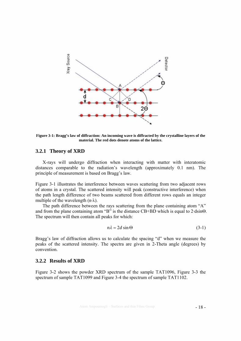
Figure 3-20: The lever rule as it applies to the eutectic composition. The exact ratio with which the two phases (CrVO4, V2O5) will crystallize can be
estimated using the lever rule (Figure 3-20). This rule states that the ratio with which the two solids will crystallize out of the system will be equal to the ratio of lengths of lines AC and CB (Figure 3-20). The line AB is called a tie-line. In our case AC/AB = ~20/50 (denoting the percentage of chromium-containing compound that will form, 40%) and CB/AB = ~30/50 (denoting the percentage of vanadium oxide that will form, 60%). Returning to Figure 3-19, after all Cr has been removed from the melt by crystallization of Cr-compounds, the system will move from point 4 to point 5 and will then keep cooling downwards to point 6. This point has the exact same composition as point 1 where we started which is logical since the original composition (97.41% V2O5 and 2.59% Cr2O3) has not changed.
By this analysis we aimed to explain some experimental findings such as the fact that the sample contains particles of completely different morphology, the fact that (as EDX analysis shows in section 3.3.2) most particles contain absolutely no Cr and the lamellar appearance of some of the particles.
In order to produce particles of homogeneous composition the process would have to involve controlled non-equilibrium cooling of the system and controlled stoichiometry of the O2 gas which was not possible with the available CVD equipment.
3.5 Raman spectroscopy By Raman spectroscopy we aim to analyze specifically the carbon layers that
surround our compound. Using Raman spectroscopy we probe the hybridization of the carbon layers and therefore their crystallinity.
The Raman spectra were recorded at the University of Ioannina using a micro-Raman system RM-1000 Renishaw, using 0.5 to 1 mW laser excitation line at 532 nm (Nd-YAG) with a 1 μm focus spot.
Asem Ampoumogli – Surfaces and thin Films Group
- 38 -
3.5.1 Theory of Raman Spectroscopy
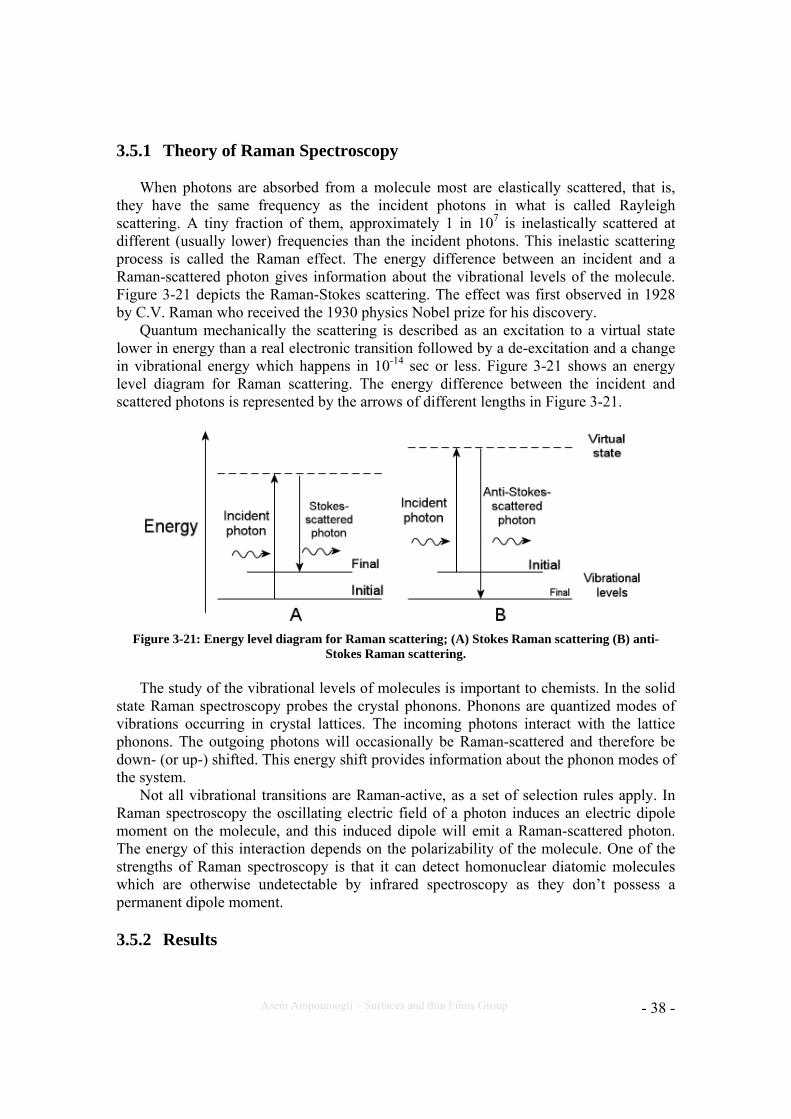
When photons are absorbed from a molecule most are elastically scattered, that is, they have the same frequency as the incident photons in what is called Rayleigh scattering. A tiny fraction of them, approximately 1 in 107 is inelastically scattered at different (usually lower) frequencies than the incident photons. This inelastic scattering process is called the Raman effect. The energy difference between an incident and a Raman-scattered photon gives information about the vibrational levels of the molecule. Figure 3-21 depicts the Raman-Stokes scattering. The effect was first observed in 1928 by C.V. Raman who received the 1930 physics Nobel prize for his discovery.
Quantum mechanically the scattering is described as an excitation to a virtual state lower in energy than a real electronic transition followed by a de-excitation and a change in vibrational energy which happens in 10-14 sec or less. Figure 3-21 shows an energy level diagram for Raman scattering. The energy difference between the incident and scattered photons is represented by the arrows of different lengths in Figure 3-21.
Figure 3-21: Energy level diagram for Raman scattering; (A) Stokes Raman scattering (B) anti-
Stokes Raman scattering.
The study of the vibrational levels of molecules is important to chemists. In the solid state Raman spectroscopy probes the crystal phonons. Phonons are quantized modes of vibrations occurring in crystal lattices. The incoming photons interact with the lattice phonons. The outgoing photons will occasionally be Raman-scattered and therefore be down- (or up-) shifted. This energy shift provides information about the phonon modes of the system.
Not all vibrational transitions are Raman-active, as a set of selection rules apply. In Raman spectroscopy the oscillating electric field of a photon induces an electric dipole moment on the molecule, and this induced dipole will emit a Raman-scattered photon. The energy of this interaction depends on the polarizability of the molecule. One of the strengths of Raman spectroscopy is that it can detect homonuclear diatomic molecules which are otherwise undetectable by infrared spectroscopy as they don’t possess a permanent dipole moment.
3.5.2 Results

Asem Ampoumogli – Surfaces and thin Films Group
- 39 -
The recorded Raman spectra for all the sample series are shown in Figure 3-22:
Figure 3-22: Raman spectra of the samples.
The spectra have three main peaks in the Raman shift range 1200 – 1800 cm-1: The D (for Disorder, centered around 1352 cm-1), the G (for Graphite, centered around 1603 cm-
1) and the M (centered around 1805 cm-1) . The peak positions are shown in Table 3-3.
D band G band M band Sample Position
[cm-1] inensity Position [cm-1] intensity Position
[cm-1] ID/IG
TAT1096 1345 334 1598 410 1788 0,82 TAT1097 1335 475 1606 587 1794 0,81 TAT1098 1343 1459 1606 1806 1809 0,81 TAT1099 1350 281 1604 342 1788 0,82 TAT1100 1348 144 1606 166 1799 0,87 TAT1101 1343 425 1609 520 1791 0,82 TAT1102 1348 127 1591 165 1796 0,77
Table 3-3: The Raman shifts and peak intensities as fitted from the spectra.
The G band corresponds to the tangential stretching mode (E2g) of highly oriented
pyrolytic graphite and can be used to assess the degree of crystallinity [39] of the carbon

Asem Ampoumogli – Surfaces and thin Films Group
- 40 -
layers. For pure crystalline graphite this band appears at ca. 1581 cm-1 [39]. This band is actually the only theoretically Raman active mode of the infinite lattice [40]. At least part
Figure 3-23: Raman modes of the infinite graphite lattice.
of this band is contributed by the D' which has been reported for microcrystalline graphite and pristine HOPG [41].
The D band is caused by breakdown of the solid state Raman selection rules which prevent its appearance in the spectrum of the perfect crystal. It originates from disorder in the sp2-hybridized carbon atoms. For pyrolytic graphite the band appears from 1348 cm-1 [39] to 1370 cm-1 [42]. The relative intensity of the D and G bands depends on the crystal planar domain size of graphite [39] and therefore reveals the degree of disorder [18]. The values calculated for our material (shown in Table 3-3) are similar to those reported for carbon nanotubes prepared using acetylene [43]. This is encouraging as these are the same results derived from the paper by L. Jancovic and D. Gournis [18] on which this project is based, which reported the success of CVD in the synthesis of Sn-filled nanotubes. The technique used in both cases was CVD, starting from a powder of the material we desired to have encased in carbon. In the case of the aforementioned paper though the outcome was actually nanotubes, but the Raman measurements we performed confirm that high quality (i.e. highly crystalline) graphite can be found on the surface of our particles. From the TEM observations we know that they are not homogeneous which is in large contrast with the aligned graphite that make up the walls of nanotubes.
The origin of the band centered around 1805 cm-1 is not entirely clear. The closest assignment we could make is that this is an M band which is an overtone of the infrared-active “out-of-plane” mode found at ca. 864 cm-1 in graphite [41] consisting of two shoulders at 1745 cm-1 and 1788 cm-1.

Asem Ampoumogli – Surfaces and thin Films Group
- 41 -
Chapter 4 Catalytic Properties
4.1 Catalytic Measurements To verify that the synthesized material did act as a catalyst we conducted a series of
catalytic tests. The reaction our material catalyzed was the assymetric oxidation of methyl-phenyl-sulfide to sulfoxide and sulfone [44], shown in Figure 4-1.
Our motivation for choosing this reaction was firstly that there are many precedents of this reaction being used to estimate the catalytic activity of vanadium complexes [44], and secondly it is very easy to monitor the change of the NMR signal of the methyl group as the molecule is oxidized to sulfoxide and then to sulfone.
SC H 3
SC H 3
O
SC H3
O O
methyl-phenyl-sulfide methyl-phenyl-sulfoxide methyl-phenyl-sulfone
+
Figure 4-1: The asymmetric oxidation of methyl-phenyl-sulfide (also Ph-S-Me or thioanisole) to methyl-phenyl-sulfoxide and the corresponding sulfone. This reaction was successfully catalyzed by
our material.
We performed four catalytic experiments in which the catalysts differed. The experiments are summarized in the following table:
Reaction number Catalyst Duration of the
reaction
1 TAT 1102 (V2O3
encased in graphite, undoped)
48 hrs
2 TAT 1102 (V2O3
encased in graphite, undoped)
1 week
3 None (blank reaction) 1 week
4 TAT 1099
(V2O3 encased in graphite,Cr-doped)
1 week
5 Pure V2O3 1 week
Table 4-1: The catalytic experiments performed.

Asem Ampoumogli – Surfaces and thin Films Group
- 42 -
Figure 4-2: The setup for the catalytic reactions. The reaction was carried out in a spherical vial in N2.
The general procedure for the catalytic experiments is as follows:
To a solution of the methyl-phenyl-sulfide (0.04 mmol, 0.48 mL) in 2 mL of DCM (di-chloro methane used as a solvent), we added 0.04 mmol (6 mg) of the catalyst. H2O2 (4.4 mmol, 0.16 mL) was added drop-wise over approximately 1 hour and the resulting mixture was stirred for the duration of the experiment. H2O2 provides the oxygen for the reaction. The reaction was quenched with 2.0 mL of H2O and the solution was extracted with ethyl acetate (3 x 10 mL) (Figure 4-3). All syntheses and manipulations were carried out under dry nitrogen atmosphere.
To fully remove all remaining water, the organic phase was dried with anhydrous NaSO4 and concentrated to give a yellowish oil. The products were separated by column chromatography with ethyl acetate (EtOAc) as eluent (Figure 4-4). During this process the concentrated reaction mixture (containing unreacted sulfide and the two products sulfoxide and sulfone) is put through a glass column filled with silica gel which is a finely particulate inactive medium called the stationary phase. Solvent (in this case called the eluent) is constantly poured on the top of the column. As the eluent moves through the column it carries the different compounds down with it but at different speeds. The elution speed depends on the solubility of each compound in the particular eluent and additionally, on the strength with which each compound adsorbs on the silica particles.
For the first experiment we used undoped V2O3 with graphite layers (compound TAT1102, reaction 1) and this was left to react for 48 hrs. The experiment showed definite catalytic potential, however, it was decided that 1 week was more appropriate to allow the reaction to go to the full extent, thus the experiment was repeated but left for 1 week (reaction 2). Then to verify the catalytic action we performed a blank experiment, that is, the same exact experiment but without the catalyst in what we name catalytic reaction 3. Ideally, oxidation should occur only in the catalyzed reaction.
To compare the reactivity of the doped compounds we carried out reaction number 4 using sample TAT1099, a Cr-doped sample in the middle of the doping range, which we consider representative of our materials. Finally this was followed by a catalytic reaction

Asem Ampoumogli – Surfaces and thin Films Group
- 43 -
using pure (i.e. without graphitic layers) V2O3 (from “Alfa Inorganics”). The catalytic action of the catalyst was appreciated by comparing the relative quantities of the two oxidized compounds as these were measured by 1H and 13C NMR (section 4.1.2).
Figure 4-3: The setup for the extraction.
Figure 4-4: Column chromatography at the beginning (left) and after some time (right). The separation of the organic compounds on the right image is shown exaggerated for clarity.

Asem Ampoumogli – Surfaces and thin Films Group
- 44 -
For example, the more polar a molecule is, the stronger it adsorbs. In our case, the
sulfone is the most polar moiety (because of the two S=O bonds, Figure 4-1) followed by the sulfoxide and finally the sulfide. The eluent that comes out the end of the column is collected in numbered test tubes which are checked by Thin-Layer Chromatography (TLC, section 4.1.1) for the presence of the compounds. Due to of the different elution speeds, each of the compounds will appear in different tubes.
The progress of the reaction was monitored by TLC (Thin-Layer Chromatography, section 4.1.1) and 1H and 13C NMR (section 4.1.2).
4.1.1 Thin Layer Chromatography
Thin-Layer Chromatography (TLC) is frequently used as a quick chemical analysis to indicate the appearance of a new compound in a reaction mixture. A TLC plate is a sheet of aluminium coated on one side with a thin layer of silica gel in the form of white powder which acts as an absorber. A scheme of this process is shown in Figure 4-5.
Using a capillary pipette, we place a drop of a solution of the initial compound near the bottom of the plate, the spot marked R (for ’reagent’) in Figure 4-5. Next to that we place a drop of the reaction mixture in the spot marked P, for ’product’. The plate is then developed. This is done by placing the plate in a shallow pool of a solvent so that only the very bottom of the plate, exactly below where we placed the two drops, is in the solvent. The solvent, in this case called the eluent, will slowly rise up the plate by capillary action and will carry the various compounds up with it. Different components will have different solubility in the eluent and will adsorb on the silica with dissimilar strengths.
Therefore, some components will be carried further up the plate. The dominant forces between silica and the compounds are dipole-dipole intractions. Polar molecules will
Figure 4-5: A scheme of the TLC process: A) Before the eluent has had time to move up the plate. B) After the eluent has carried the two compounds up the plate, marks at different heights can be seen
under UV irradiation.

Asem Ampoumogli – Surfaces and thin Films Group
- 45 -
interact more strongly with the fine silica particles, while less polar molecules are adsorbed less tightly and will move faster through the adsorbent. In our case we expect that the sulfoxide and the sulfone traverse the plate slower than the sulfide due to the polar S=O group and this was what we saw.
The choice of eluent is important because it must be such that both compounds will be carried by it but not at very different rates. In our case this was a 1:2 mixture of ethyl acetate and heptane.
After the eluent has moved all the way up the plate, the plate is removed from the eluent bath. If the compounds are coloured visualization is straightforward, else fluorescent dyes and a UV lamp are used to see the compounds. In our case both the sulfide and the sulfoxide are UV-active so no dye was needed.
TLC is a very useful technique for quickly getting an idea of what exists in the reaction mixture. The actual verification however of the existence of the reaction products and a relative quantification is given by 1H and 13C NMR ( section 4.1.2).
4.1.2 1H and 13C NMR
All nuclei that contain odd numbers of protons or neutrons have an intrinsic magnetic moment and angular momentum. It is the atoms containing these nuclei that can be probed by NMR. The most commonly measured nuclei are hydrogen-1 and carbon-13, although nuclei from isotopes of many other elements (e.g. 15N, 14N, 17O, 23Na, 195Pt) can also be measured. The overall spin quantum number (I) of these nuclei is non-zero. A non-zero spin is associated with a non-zero magnetic moment, μ, via the equation
Ι⋅= γμ (4-1)
where the proportionality constant, γ, is the gyromagnetic ratio. The angular momentum associated with nuclear spin is quantized. This means that the
magnitude of angular momentum is quantized (i.e. I can only take on a restricted range of values), and also that the 'orientation' of it is quantized. This is described by the magnetic quantum number, m, which can take values from +I to –I in integral steps. Hence for any given nucleus, there is a total of 2I+1 angular momentum states. Therefore, a nucleus which has a spin of ½ (like 1H or 13C) has two possible spin states, m = ± ½. The energies of these states are degenerate, hence at thermal equilibrium the populations of these two states will be equal. This degeneracy is lifted when the nucleus is placed in a magnetic field B0 as nuclei will then be aligned either along or against the applied field. This will lead to the differently aligned nuclei having an energy difference ΔΕ given by:
0Β⋅⋅=ΔΕ γh (4-2)
Resonant absorption will occur when we apply electromagnetic radiation of the correct frequency, in the radio frequency range. This resonant absorption is detected in NMR.
It might appear then that all 1H or 13C would resonate at the same frequency for a given magnetic field, but this is not the case. The electrons of surrounding nuclei will produce a shielding effect on the measured nuclei. This shielding will reduce the

Asem Ampoumogli – Surfaces and thin Films Group
- 46 -
magnetic field that the nucleus “feels” and hence the frequency at which the nucleus will resonate. This shift due to the chemical environment is called the chemical shift. Using this information it is possible from an NMR spectrum to identify the number and relative abundance of the hydrogen (or carbon) nuclei present on the molecule that have a different chemical environment.
4.1.2.1 Results
The peaks of the 1H and 13C NMR measurements of the products of the catalytic reactions are presented here. Assignments of the peaks were according to literature [45].
1H and 13C NMR spectra were recorded on a Varian Mercury Plus spectrometer (at 400 MHz) at ambient temperature. Chemical shifts are denoted in δ (ppm) with respect to TMS and referenced to the residual CHCl3 peaks. Coupling constants J, are denoted in Hz. Product catalyst 1 (TAT1102, 48h reaction time). Yellow liquid. 1H NMR (200 MHz, CDCl3): δ 7.95 (d, J=6, Ph-SO2-Me), 7.68-7.61 (m, Ph-SO2-Me), 7.57-7.50 (m, Ph-SO-Me), 3.05 (s, Ph-SO2-Me), 2.72 (s, Ph-SO-Me) ppm. 13C {1H} NMR (200 MHz, CDCl3): δ 161.62, 145.71, 133.66, 130.99, 129.32, 127.33, 123.46, 77.62, 76.99, 76.36, 44.47, 43.96 ppm. Product catalyst 2 (TAT1102, 1 week reaction time). Yellow liquid. 1H NMR (200 MHz, CDCl3): δ 7.98-7.93 (m, Ph-SO2-Me), 7.68-7.60 (m, Ph-SO2-Me), 7.59-7.49 (m, Ph-SO-Me), 3.06 (s, Ph-SO2-Me), 2.73 (s, Ph-SO-Me) ppm. 13C {1H} NMR (200 MHz, CDCl3): δ 145.69 140.56 133.64 130.98 129.30 127.30 123.45 77.62 76.99 76.35 44.46 43.93 ppm. Product without catalyst (1 week reaction time). Yellow liquid. 1H NMR (200 MHz, CDCl3): δ 7.95 (d, J=6, Ph-SO2-Me), 7.68-7.61 (m, Ph-SO2-Me), 7.58-7.50 (m, Ph-SO-Me), 3.06 (s, Ph-SO2-Me), 2.73 (s, Ph-SO-Me) ppm. 13C {1H} NMR (200 MHz, CDCl3): δ 145.57 133.57 130.89 129.22 127.18 123.34 77.64 76.99 76.34 44.35 43.83 ppm. Product catalyst 3 (TAT1099, 1 week reaction time). Yellow liquid. 1H NMR (200 MHz, CDCl3): δ 7.98-7.93 (m, Ph-SO2-Me), 7.71-7.58 (m, Ph-SO2-Me), 7.57-7.51 (m, Ph-SO-Me), 3.06 (s, Ph-SO2-Me), 2.73 (s, Ph-SO-Me), 1.26 (s, Ph-SO-Me), 0.88-0.83 (t, Ph-SO-Me) ppm. 13C {1H} NMR (200 MHz, CDCl3): δ 140.53 133.63 130.98 129.31 127.27 123.43 77.62 76.99 76.36 44.43 43.90 31.86 29.63 29.29 22.63 14.07 ppm. Product catalyst 4 (Pure V2O3, 1 week reaction time). Yellow liquid. 1H NMR (200 MHz, CDCl3): δ 7.97-7.94 (d, J=6, Ph-SO2-Me), 7.68-7.61 (m, Ph-SO2-Me), 7.58-7.51 (m, Ph-SO-Me), 3.06 (s, Ph-SO2-Me), 2.73 (s, Ph-SO-Me) ppm. 13C {1H} NMR (200 MHz, CDCl3): δ 171.01 145.66 133.60 130.93 129.26 128.71 127.26 126.52 123.39 60.28 44.40 43.88 29.60 20.94 14.12 ppm.
The original purpose of conducting the catalytic experiments was to verify whether
our material can be used as a catalyst although it is encapsulated in the carbon layers. The

Asem Ampoumogli – Surfaces and thin Films Group
- 47 -
oxidation of sulfide to sulfoxide and then sufone is the experimental verification. If the material is a good catalyst it should assist in the conversion of sulfide to sulfoxide and then to the doubly-oxidized sulfone.
The ratio of the peak integrals for the methyl groups of the sulfone and the sulfoxide is proportinal to the relative abundance of the two products. This is summarized in table Table 4-2. The reactions are given in order of decreasing efficiency.
Relative percentage Reaction catalyst Sulfoxide Sulfone
TAT1099, 1 week 27% 73% TAT1102, 1 week 67% 33% TAT1102, 48 hrs 72% 28%
Pure V2O3 85% 15% Blank, 1 week 90% 10%
Table 4-2: Summary of the efficiency of the catalysts.
It is clear from Table 4-2 that the catalytic efficiency of the doped catalyst (TAT1099)
is the highest, showing the biggest sulfone yield. The sample TAT1102 (vanadium oxide encased in carbon layers) is substantially more efficient than pure V2O3 and the blank experiment had the lowest efficiency of all the experiments because it produced the least amount of sulfone. The higher catalytic activity of the doped compound could be due to the CrVO4 particles which are themselves catalysts [46].
4.2 The Catalyst After Application After the sample TAT1102 and the pure V2O3 had been used as catalysts we
examined them with SEM to see any changes that had taken place in the material. We found that the morphology of the samples had changed drastically. This was already quite obvious after the catalytic test when we removed part of the used catalyst from the reaction vial. The powder morphology had disappeared and instead the material was a flabby substance.
This observation can be verified with the SEM micrographs presented here. In Figure 4-6 on the left, we show a SEM micrograph of the pure V2O3 sample after it had been used as a catalyst. The particles that made up the catalyst have disappeared. Instead what we find is a new phase of the material that is dispersed on the sample substrate. On the right we show a detail of the surface of this new phase. What we can see is that it has a fibrous composition. In the relevant literature we can find that the material V2O5 is actually considered an inorganic polymer [47] and that it has been reported that hydrogen peroxides (which we actually used in the catalysis procedure) react with V2O5 to produce a red gelatinous product [48]. Fibers of V2O5 (but not V2O3) can easily be produced and bear a resemblance to our material [48]. From this we can deduce that the V2O3 we originally had as our catalyst has been oxidized to V2O5.

Asem Ampoumogli – Surfaces and thin Films Group
- 48 -
Figure 4-6: SEM micrographs of the pure V2O3 sample after it was reclaimed from the reaction vial. On the left we show an overview of the sample. On the right we show a close detail of the texture of
this material.
In the following micrographs (Figure 4-7) we show the appearance of the sample TAT1102 (the undoped oxide particles) after they had been used as a catalyst. On the left there is an overview of the material and on the right a close-up detail.
Two spots we measured by EDX on this material (TAT1102) showed that it is comprised of 18% C, 40% O and 43% V in one spot and 31% C, 36% O and 33% V in the second (in atomic percentages). In the original composition of this sample the ratio between vanadium and oxygen was 2/5 V and 3/5 O. We see that this relative ratio between V, O has changed and that some oxygen has been depleted. We also deduce that the composition of this soft new phase is not homogeneous.
It is important to mention that we did not attempt to re-use a catalyst after the reaction had been completed. It is quite obvious that the material has significantly changed after its use, i.e. the particles have morphed into a new phase and the carbon layers are no
Figure 4-7: SEM micrographs of the sample TAT1102. On the left we show an overview of the material and on the right a detail of it.

Asem Ampoumogli – Surfaces and thin Films Group
- 49 -
longer protecting the material against oxidation while in storage. This could mean than it is no longer active as a catalyst, however, this has to be verified by re-using the material.

Asem Ampoumogli – Surfaces and thin Films Group
- 50 -
Chapter 5 Synopsis
5.1 Conclusions From the study of the material we synthesized we can draw the following conclusions:
The bulk of the material was indeed V2O3 as the XRD and the EBSD results show. The material has the form of micrometer size particles, which are not homogeneous in size, shape or composition, because of the synthesis conditions. The aim of doping the material in a controlled fashion was not possible with the available equipment hence most of the particles are actually not doped with chromium, as the analysis of the ceramic melt shows. In order to produce samples consisting of homogeneously doped particles with a narrow size distribution, we should have used equipment which would allow precise manipulations of the temperature during the CVD process. The Si contamination could have been avoided by using a CVD boat made of a material that would not be decomposed because of the reactions taking place inside it.
The XRD analysis proved to be very important in analyzing the bulk of our material. One of the difficulties we came across was trying to measure the amount of Cr in our
samples. The compound CrVO4 which we assume has been synthesized during the cooling of the melt could not be seen in the XRD because of the nature of the domains it forms so we can only speculate about whether it is actually to be found in our material, since we were unable to spot a particle with this elemental composition by EDX.
Electron microscopy played a very important part in this project. We were able to verify the existence of the carbon layers by TEM. By SEM we made the bulk of the observations regarding the material and we drew the most conclusions about it.
The carbon layers that surround our particles are of good crystallization as the Raman spectra show, so the CVD process can successfully be used for encasing nanoparticles.
By the catalytic testing we were able to verify that our material can act as a catalyst despite the carbon encasement, an important fact
The material is catalytically active in the case of the examined reaction and the doped samples are more catalytically active. The observation that the nature of our catalyst completely changed is not very encouraging concerning the re-usability of the material as a catalyst.

Asem Ampoumogli – Surfaces and thin Films Group
- 51 -
Chapter 6 Bibliography 1. Weckhuysen, B.M. and D.E. Keller, Chemistry, spectroscopy and the role of
supported vanadium oxides in heterogeneous catalysis. Catalysis Today, 2003.
78(1): p. 25--46.
2. Ramana, C.V., et al., Formation of V2O3 nanocrystals by thermal reduction of
V2O5 thin films. Solid State Communications, 2006. 137(12): p. 645-649.
3. Surnev, S., M.G. Ramsey, and F.P. Netzer, Vanadium oxide surface studies.
Progress in Surface Science, 2003. 73(4): p. 117--165.
4. Bao, W., et al., Magnetic correlations and quantum criticality in the insulating
antiferromagnetic, insulating spin liquid, renormalized Fermi liquid, and metallic
antiferromagnetic phases of the Mott system V_ {2} O_ {3}. Physical Review B,
1998. 58(19): p. 12727-12748.
5. Imada, M., A. Fujimori, and Y. Tokura, Metal-insulator transitions. Reviews of
Modern Physics, 1998. 70(4): p. 1039-1263.
6. Zheng, C., et al., Preparation and characterization of spherical V2O3
nanopowder. Journal of Solid State Chemistry, 2003. 170(2): p. 221-226.
7. Do Hong Thanh, P.D.L., V.T. Bich, and N.N. Dinh, Structural Formation And
Raman Scattering Spectrum of Vanadium Oxide ThinFilms made By electron
Beam Deposition. Communications in Physics, 1998. 8(3): p. 152-158.
8. Pan, Y., G.Z. Wu, and X.S. Yi, Vanadium sesquioxide-polymer composites: the
study of electrical conductivity. Journal of Materials Science, 1994. 29(21): p.
5757-5764.
9. Wei, L., et al., Preparation and characterization of (V Cr x) 2 O 3 nano-powders
by chemical doping method. Materials Science and Engineering: B, 2006. 131(1-
3): p. 116-120.
10. Zhang, K., et al., A new method for preparing V2O3 nanopowder. Materials
Letters, 2005. 59(22): p. 2729-2731.

Asem Ampoumogli – Surfaces and thin Films Group
- 52 -
11. Mathur, S., T. Ruegamer, and I. Grobelsek, Phase-Selective CVD of Vanadium
Oxide Nanostructures. CHEMICAL VAPOR DEPOSITION-WEINHEIM-, 2007.
13(1): p. 42.
12. Hojo, J.I., O. Iwamoto, and A. Kato, Formation of Fine Vanadium Nitride
Powders by Cvd Method. Nippon Kagaku Kaishi, 1975(5): p. 820-825.
13. Chen, Y. and I.E. Wachs, Tantalum oxide-supported metal oxide (Re2O7, CrO3,
MoO3, WO3, V2O5, and Nb2O5) catalysts: synthesis, Raman characterization
and chemically probed by methanol oxidation. Journal of Catalysis, 2003. 217(2):
p. 468-477.
14. Ballarini, N., et al., The oxygen-assisted transformation of propane to COx/H2
through combined oxidation and WGS reactions catalyzed by vanadium oxide-
based catalysts. Catalysis Today, 2006. 116(3): p. 313-323.
15. Schoiswohl, J., et al., Vanadium oxide nanostructures: from zero-to three-
dimensional. J. Phys.: Condens. Matter, 2006. 18: p. R1-R14.
16. Goward, G.R., F. Leroux, and L.F. Nazar, Poly (pyrrole) and poly
(thiophene)/vanadium oxide interleaved nanocomposites: positive electrodes for
lithium batteries. Electrochimica Acta, 1998. 43(10-11): p. 1307-1313.
17. Patzke, G.R., F. Krumeich, and R. Nesper, Oxidic nanotubes and nanorods--
anisotropic modules for a future nanotechnology. Angew Chem Int Ed Engl, 2002.
41(14): p. 2446-61.
18. Jankovic, L., et al., Carbon Nanotubes Encapsulating Superconducting Single-
Crystalline Tin Nanowires. Nano Lett, 2006. 6(6): p. 1131--1135.
19. D.A. Pears, S.C.S., Polyurea-Encapsulated Palladium Catalysts: The
Development and Application of A New Versatile Immobilised Homogeneous
Catalyst Technology. Aldrichimica Acta, 2005. 38(1): p. 23-33.
20. Mott, N.F., Metal-Insulator Transition. Reviews of Modern Physics, 1968. 40(4):
p. 677.
21. Yethiraj, M., Pure and doped vanadium sesquioxide: a brief experimental review.
Journal of Solid State Chemistry, 1990. 88(1): p. 53--69.

Asem Ampoumogli – Surfaces and thin Films Group
- 53 -
22. Di Matteo, S., N.B. Perkins, and C.R. Natoli, Spin-1 effective Hamiltonian with
three degenerate orbitals: An application to the case of V_ {2} O_ {3}. Physical
Review B, 2002. 65(5): p. 54413.
23. Mott, N.F., The Basis of the Electron Theory of Metals, with Special Reference to
the Transition Metals. Proceedings Of The Physical Society, Section A, 1949.
62(7): p. 416.
24. Tasaki, H., The Hubbard model-an introduction and selected rigorous results.
Journal of Physics: Condensed Matter, 1998. 10(20): p. 4353-4378.
25. Craciun, M.F., Alkali-Doped Metal-Phthalocyanine and Pentacene Compounds,
in Applied Sciences. 2006, Technische Universiteit Delft: Delft.
26. Yethiraj, M., et al., Phonon anomalies and the magnetic transition in pure and
Cr-doped V_{2}O_{3}. Physical Review B, 1987. 36(16): p. 8675.
27. Ando, Y., et al., Growing carbon nanotubes. Materials Today, 2004. 7(10): p. 22.
28. Endo, M., et al., Production and Structure of Pyrolytic Carbon Nanotubes
(PCNTs). J. Phys. Chem. Solids, 1993. 54(12): p. 1841--1848.
29. Dai, H., et al., Single-wall nanotubes produced by metal-catalyzed
disproportionation of carbon monoxide. Chem. Phys. Lett, 1996. 260(3-4): p.
471--475.
30. McWhan, D.B. and J.P. Remeika, Metal-Insulator Transition in [V(1-
x)Cr(x)]2O(3). Physical Review B, 1970. 2(9): p. 3734--3750.
31. Honig, J.M. and J. Spalek, Metal-Insulator Transitions in the V2O3 Alloy System:
Experiment and Theory. Proc. Indian Sci. Acad., 1986. 52 A(No 1): p. 232-264.
32. Zylbersztejn, A. and N.F. Mott, Metal-insulator transition in vanadium dioxide.
Physical Review B, 1975. 11(11): p. 4383-4395.
33. McClune, W.F., International Center for Diffraction Data. 1983.
34. Asbrink, S., The crystal structure of and valency distribution in the low-
temperature modification of V3O5. The decisive importance of a few very weak
reflexions in a crystal-structure determination. Acta Crystallographica Section B,
1980. 36(6): p. 1332-1339.

Asem Ampoumogli – Surfaces and thin Films Group
- 54 -
35. Yang, S., E. Iglesia, and A.T. Bell, Oxidative dehydrogenation of propane over
V2O5/MoO3/Al2O3 and V2O5/Cr2O3/Al2O3: structural characterization and
catalytic function. J. Phys. Chem. B., 2005. 109(18): p. 8987-9000.
36. Worle-Knirsch, J.M., et al., Nanoparticulate vanadium oxide potentiated
vanadium toxicity in human lung cells. Environmental Science & Technology,
2007. 41(1): p. 331-336.
37. Gray, M.L., et al., Crystal chemistry of V3O5 and related structures. Journal of
Solid State Chemistry, 1986. 62(1): p. 57-63.
38. E. M. Levin, C.R.R., H.F. McMurdie, Phase Diagrams For Ceramists, ed. M.K.
Reser. 1964, Ohio: The American Ceramic Society.
39. Li, W., et al., Raman characterization of aligned carbon nanotubes produced by
thermal decomposition of hydrocarbon vapor. Applied Physics Letters, 1997. 70:
p. 2684.
40. Filik, J., Raman Spectroscopy: A simple, non-destructive way to characterize
diamond and diamond-like materials. Spectroscopy Europe, 2005. 17(5).
41. Tan, P.H., S. Dimovski, and Y. Gogotsi, Raman scattering of non-planar graphite:
arched edges, polyhedral crystals, whiskers and cones. Philosophical
Transactions: Mathematical, Physical and Engineering Sciences, 2004. 362(1824):
p. 2289-2310.
42. Reich, S. and C. Thomsen, Raman spectroscopy of graphite. Philosophical
Transactions: Mathematical, Physical and Engineering Sciences, 2004. 362(1824):
p. 2271-2288.
43. Sveningsson, M., et al., Raman spectroscopy and field-emission properties of
CVD-grown carbon-nanotube films. Applied Physics A: Materials Science &
Processing, 2001. 73(4): p. 409-418.
44. Hsieh, S.H., Y.P. Kuo, and H.M. Gau, Synthesis, characterization, and structures
of oxovanadium (V) complexes of Schiff bases of-amino alcohols as tunable
catalysts for the asymmetric oxidation of organic sulfides and asymmetric
alkynylation of aldehydes. Dalton Trans, 2007. 97: p. 106.
45. E. Pfetch, P.B., C. Affolter, Structure Determination of Organic Compounds.
2004: Springer.

Asem Ampoumogli – Surfaces and thin Films Group
- 55 -
46. Shishido, T., et al., Vapor-phase oxidation of 3-picoline to nicotinic acid over
Cr1-xAlxVO4 catalysts. Applied Catalysis a-General, 2003. 239(1-2): p. 287-296.
47. Achard, M.F., et al., Macroscopic Fibers of Oriented Vanadium Oxide Ribbons
and Their Application as Highly Sensitive Alcohol Microsensors*. Adv. Mater,
2005. 17: p. 2970-2974.
48. Livage, J., Vanadium pentoxide gels. Chemistry of Materials, 1991. 3(4): p. 578-
593.

Asem Ampoumogli – Surfaces and thin Films Group
- 56 -
Chapter 7 Acknowledgements
The acknowledgements a person receives on the last pages of a Master thesis do not really add to their professional merit in the same way that the references found on the thesis are not really considered citations. This however means in no way that the guidance and assistance were not real or that the gratitude expressed is not sincere! Helping someone understand how scientific research works is not easy and it requires a lot of patience, understanding and real expertise. I am very fortunate to have found these in the following people whom I would sincerely like to thank:
Prof. Dr. Petra Rudolf of the Surfaces And Thin Films of the Rijksuniversiteit Groningen for assigning me the Master project and heartily accepting me in her group where I have found an ideal environment for me to realize my potential and for being a very understanding person.
Prof. Dr. Ir. A.J. Minnaard of the Bio-Organic Chemistry group for agreeing to referee my thesis and presentation and for his time and expertise.
Prof. Dr. Dimitris Gournis of the University Of Ioannina for all his involvement with my choice of my master studies and for all his assistance and time over my project as well as for allowing the use of the materials synthesis lab of the Materials Science and Engineering department in the University Of Ioannina where the synthesis took place.
Prof. Dr. B.L. Feringa of the Synthetic Organic Chemistry group for allowing the use of his organic synthesis lab, where the catalytic measurement were performed.
PhD students Régis Gengler and Tatiana Fernández Landaluce of the Surfaces And Thin Films group for their continuous assistance, corrections, professionalism and all the time they took out of their busy schedule so that this thesis might be completed. Without their supervision this thesis would never have amounted to anything.
PhD student Thodoris Tsoufis of the Department of Materials Science and Engineering of the University Of Ioannina for all his help with the synthesis and the measurements that he did and for being my closest associate in Greece throughout this time.
Technician J. Baas of the group of Prof. Dr. T.T.M. Palstra for performing the XRD experiments and for his help and explanations.
Technician Gert ten Brink of the Materials Science group of Prof. Dr. J.T.M. de Hosson for the SEM/EDX/EBSD measurements that he performed and for all his time and enlightening discussions.
Associate Professor Dr. Ir. B.J. Kooi of the Materials Science group for the TEM/EDX measurements and for all his precious time and help.

Asem Ampoumogli – Surfaces and thin Films Group
- 57 -
Postdoctoral researcher Dr. Antony V. Kazantzis of the Materials Science group for the SEM/EDX measurements, for his help with the analysis of the ceramic melt and for his help and enlightening discussions.
PhD student Ir. Ji Liu of the Physics of Nanodevices group for finding the time to train us in using the SEM of her group. All the people of the Surfaces And Thin Films group for all their help and for being at once professional, helpful and friendly.