Embed Size (px)
Citation preview
Prepared By :A.PandianA.SuganyaS.Abirami
VALLIAMMAI ENGINEERING COLLEGE SRM Nagar, Kattankulathur – 603 203.
DEPARTMENT OF ELECTRONICS & COMMUNICATION ENGINEERING
QUESTION BANK
SUBJECT : EC6304/ ELECTRONIC CIRCUITS-1
SEM / YEAR: III/ II Year ECE
UNIT I
POWER SUPPLIES AND BIASING OF DISCRETE BJT AND
MOSFET
Rectifiers with filters- DC Load line, operating point, Various biasing methods for BJT-Design-
Stability-Bias compensation, Thermal stability, Design of biasing for JFET, Design of biasing for
MOSFET
PART A
Q.No Questions BT
Level Competence
1. What is need of Biasing? BTL 1 Remembering
2. Draw D.C load line. BTL 1 Remembering
3. Define stability factor. BTL 1 Remembering
4. Discuss about operating point. BTL 1 Remembering
5. Show the equations for the stability factors
S’ and S’’.
BTL 1 Remembering
6. How to find the expression for stability factor? BTL 1 Remembering
7. Summarize the requirements for biasing circuits? BTL 2 Understanding
8. Illustrate the main idea of compensation techniques? BTL 2 Understanding
9. When the thermal runway happens at the amplifier
circuit?
BTL 2 Understanding
10. Give outline for compensation techniques? BTL 2 Understanding
11. Identify the operating regions of N-channel MOSFET
and how do you identify the operating region?
BTL 3 Applying
12. Categorize the different methods of biasing a
JFET?
BTL 3 Applying
13. How would you apply various conditions for thermal
stability and What are the conditions for thermal stability? BTL 3 Applying
Prepared By :A.PandianA.SuganyaS.Abirami
14. Analyze the function of Q-point? How it varies the output? BTL 4 Analyzing
15. Examine why the operating point selected at the Centre of
the active region?
BTL 4 Analyzing
16. List out the advantages of using emitter resistance in the
context of biasing? BTL 4 Analyzing
17. Assess the importance of selecting the proper
operating point.
BTL 5 Evaluating
18. How would you explain FET is known as
voltage variable resistor?
BTL 5 Evaluating
19. Build the fixed bias single stage transistor circuit. BTL 6 Creating
20. How would you adapt a D.C load line in
fixed bias amplifier circuit?
BTL 6 Creating
PART-B
1 What is D.C. load line? How will you select the operating
point, explain it using common emitter amplifier
characteristics as an example? (13)
BTL 1 Remembering
2 Demonstrate common source self bias and voltage divider
bias for FET with neat diagrams? (13) BTL 1 Remembering
3 Find voltage divider bias circuit for NMOS such that
𝐼𝐷𝑄 = 400µ𝐴, 𝑉𝐷𝐷 = 14𝑉, 𝑉𝐷𝑆 = 2.3𝑉, 𝑘𝑛 =
µ𝑛𝐶𝑜𝑥 (𝑊
𝐿) = 1𝑚𝐴 𝑝𝑒𝑟 𝑉2 , 𝑉𝑡 = 1𝑉. Assume a current
of 1µA through R1 and R2, and 𝑉𝑠 = 1.2𝑉.(13)
BTL 1 Remembering
4 With neat diagrams, how would you show two bias
compensation techniques and state its advantages and
disadvantages. (13)
BTL 1 Remembering
5 Relate the various methods of biasing using BJT in terms
of their stability factors. (13) BTL 2 Understanding
6 (i) Illustrate stability and thermal stability. (7)
(ii) Summarize the working of Full wave rectifier with
CLC filter and derive for its ripple factor? (6)
BTL 2 Understanding
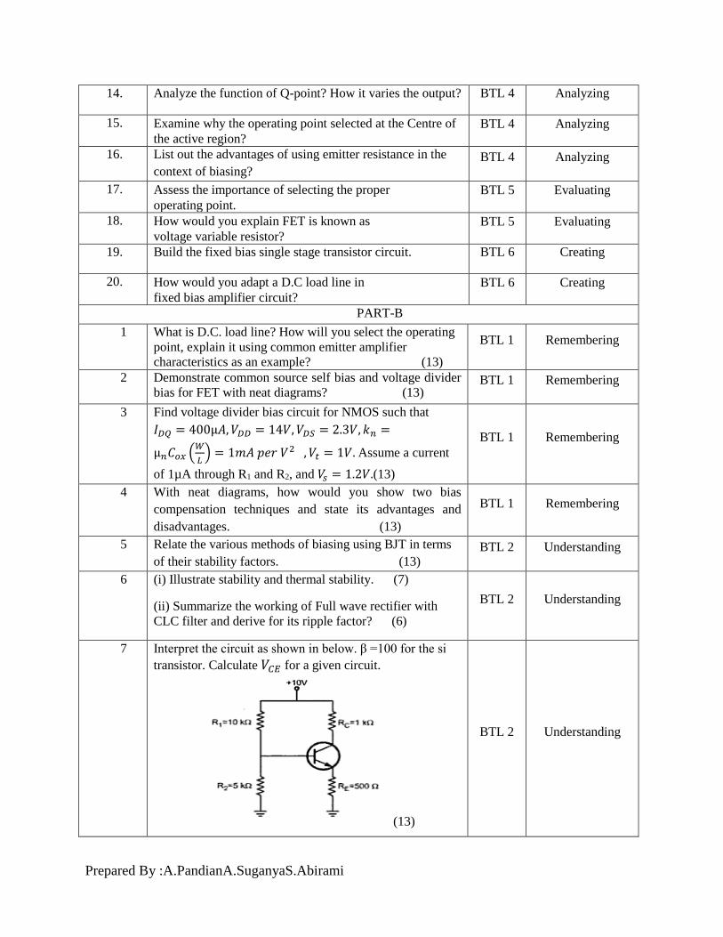
7 Interpret the circuit as shown in below. β =100 for the si
transistor. Calculate 𝑉𝐶𝐸 for a given circuit.
(13)
BTL 2 Understanding

Prepared By :A.PandianA.SuganyaS.Abirami
8 For the circuit shown in fig.𝐼𝐶=2mA, β =100 , Calculate
𝑅𝐸,𝑉𝐸𝐶 and stability factor.
(13)
BTL 3 Applying
9 The amplifier shown in Fig. an n-channel FET for which,
ID=0.8mA, VP=-20V and IDSS=1.6mA. Assume that rd>Rd.
Calculate the following parameters. (1) VGS (2) gm (3) Rs.
(13)
BTL 3 Applying
10 Analyze various techniques of stabilization of Q-point in a
transistor. (13)
BTL 4 Analyzing
11 Explain in detail about various methods of biasing
MOSFET. (13)
BTL 4 Analyzing
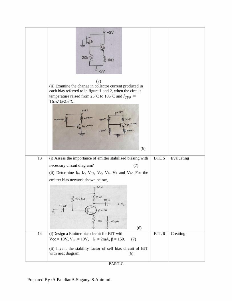
12 (i) The parameters for each transistor in the circuit in
figure are ℎ𝑓𝑒 = 100, 𝑎𝑛𝑑𝑉𝐵𝐸(𝑂𝑁) = 0.7𝑉. Examine the
Q-point values of base, collector and emitter currents in
Q1 and Q2.
BTL 4 Analyzing
Prepared By :A.PandianA.SuganyaS.Abirami
(7)
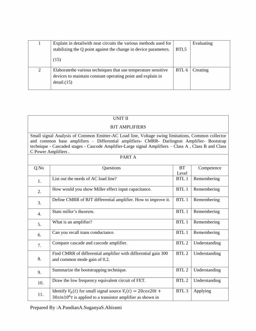
(ii) Examine the change in collector current produced in
each bias referred to in figure 1 and 2, when the circuit
temperature raised from 25°C to 105°C and 𝐼𝐶𝐵𝑂 =15𝑛𝐴@25°𝐶.
(6)
13 (i) Assess the importance of emitter stabilized biasing with
necessary circuit diagram? (7)
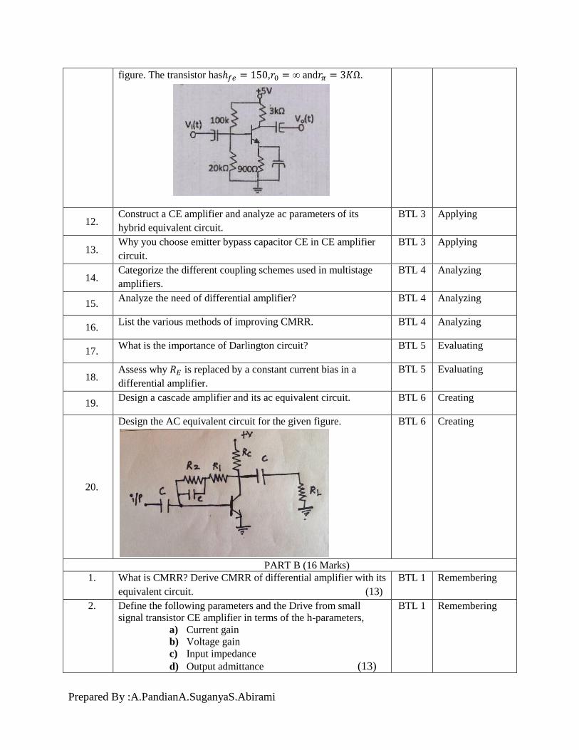
(ii) Determine IB, IC, VCE, VC, VB, VE and VBC For the
emitter bias network shown below,
(6)
BTL 5 Evaluating
14 (i)Design a Emitter bias circuit for BJT with
Vcc = 18V, VCE = 10V, IC = 2mA, β = 150. (7)
(ii) Invent the stability factor of self bias circuit of BJT
with neat diagram. (6)
BTL 6 Creating
PART-C
Prepared By :A.PandianA.SuganyaS.Abirami
1 Explain in detailwith neat circuits the various methods used for
stabilizing the Q point against the change in device parameters.
(15)
BTL5
Evaluating
2 Elaboratethe various techniques that use temperature sensitive
devices to maintain constant operating point and explain in
detail.(15)
BTL 6 Creating
UNIT II
BJT AMPLIFIERS
Small signal Analysis of Common Emitter-AC Load line, Voltage swing limitations, Common collector
and common base amplifiers – Differential amplifiers- CMRR- Darlington Amplifier- Bootstrap
technique - Cascaded stages - Cascode Amplifier-Large signal Amplifiers – Class A , Class B and Class
C Power Amplifiers .
PART A
Q.No Questions BT
Level
Competence
1. List out the needs of AC load line? BTL 1 Remembering
2. How would you show Miller effect input capacitance. BTL 1 Remembering
3. Define CMRR of BJT differential amplifier. How to improve it. BTL 1 Remembering
4. State miller’s theorem. BTL 1 Remembering
5. What is an amplifier? BTL 1 Remembering
6. Can you recall trans conductance. BTL 1 Remembering
7. Compare cascade and cascode amplifier. BTL 2 Understanding
8.
Find CMRR of differential amplifier with differential gain 300
and common mode gain of 0.2.
BTL 2 Understanding
9. Summarize the bootstrapping technique. BTL 2 Understanding
10. Draw the low frequency equivalent circuit of FET. BTL 2 Understanding
11. Identify 𝑉0(𝑡) for small signal source 𝑉𝑖(𝑡) = 20𝑐𝑜𝑠20𝑡 +
30𝑠𝑖𝑛106𝑡 is applied to a transistor amplifier as shown in
BTL 3 Applying
Prepared By :A.PandianA.SuganyaS.Abirami
figure. The transistor hasℎ𝑓𝑒 = 150,𝑟0 = ∞ and𝑟𝜋 = 3𝐾Ω.
12. Construct a CE amplifier and analyze ac parameters of its
hybrid equivalent circuit.
BTL 3 Applying
13. Why you choose emitter bypass capacitor CE in CE amplifier
circuit.
BTL 3 Applying
14. Categorize the different coupling schemes used in multistage
amplifiers.
BTL 4 Analyzing
15. Analyze the need of differential amplifier? BTL 4 Analyzing
16. List the various methods of improving CMRR. BTL 4 Analyzing
17. What is the importance of Darlington circuit? BTL 5 Evaluating
18. Assess why 𝑅𝐸 is replaced by a constant current bias in a
differential amplifier.
BTL 5 Evaluating
19. Design a cascade amplifier and its ac equivalent circuit. BTL 6 Creating
20.
Design the AC equivalent circuit for the given figure.
BTL 6 Creating
PART B (16 Marks)
1. What is CMRR? Derive CMRR of differential amplifier with its
equivalent circuit. (13)
BTL 1 Remembering
2. Define the following parameters and the Drive from small
signal transistor CE amplifier in terms of the h-parameters,
a) Current gain
b) Voltage gain
c) Input impedance
d) Output admittance (13)
BTL 1 Remembering
Prepared By :A.PandianA.SuganyaS.Abirami
3. How to make the Emitter Coupled Differential Amplifier
circuit and also explain that operation. (13)
BTL 1 Remembering
4. State and prove the Miller’s theorem, and also give examples.
(13)
BTL 1 Remembering
5. (i) Illustrate bootstrapped Darlington circuit with
neat sketch. (7)
(ii) Outline the common emitter amplifier. (6)
BTL 2 Understanding
6. Summarize the gain, input impedance and output impedance of
single stage BJT amplifier using mid band analysis. (13)
BTL 2 Understanding
7. Demonstrate the transfer characteristic of differential amplifier?
Derive it. (13)
BTL 2 Understanding
8. Construct the basic circuit of Darlington pair and explain with
mathematical substantiation. (13)
BTL 3 Applying
9. Identify the changes in the AC characteristics of a common
emitter amplifier when an emitter resistor and an emitter bypass
capacitor are incorporated in the design? Explain with
necessary equations. (13)
BTL 3 Applying
10. (i) Analyze the circuit shown in figure with the parameters
are ℎ𝑓𝑒 = 120 𝑎𝑛𝑑𝑉𝐴 = ∞. Inspect the following parameters.
(1) The current gain, voltage gain, input impedance
and output impedance.
(2) The maximum undistorted output voltage
swing.
(10)
(ii) The parameters for each transistor in the circuit in given
figure are ℎ𝑓𝑒 = 100, 𝑉𝐴 = ∞ and
BTL 4 Analyzing
Prepared By :A.PandianA.SuganyaS.Abirami
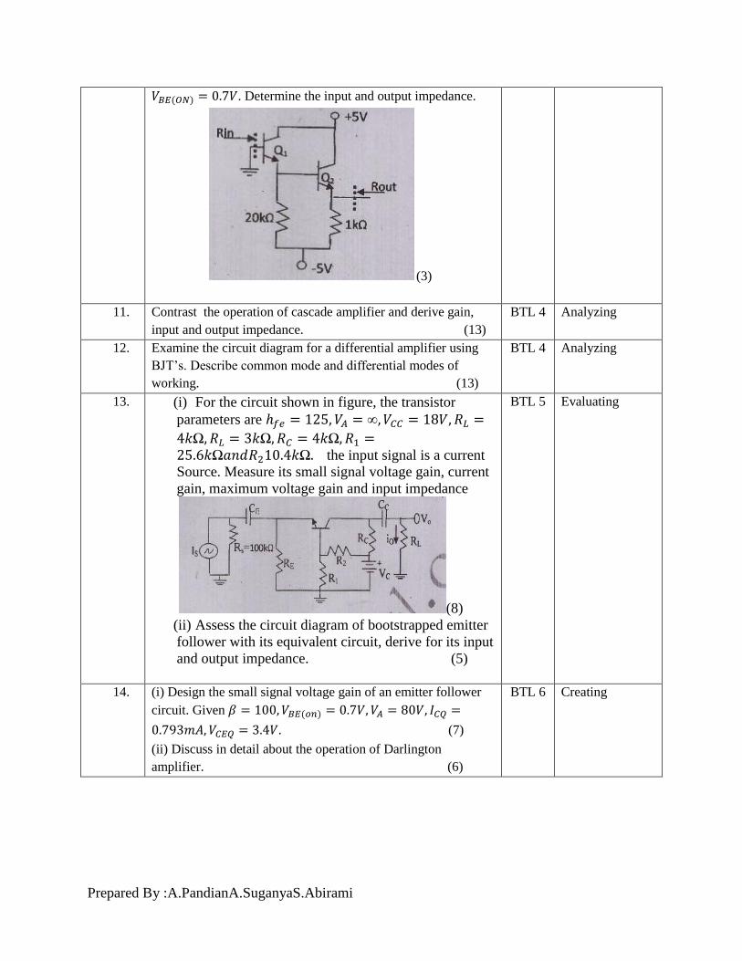
𝑉𝐵𝐸(𝑂𝑁) = 0.7𝑉. Determine the input and output impedance.
(3)
11. Contrast the operation of cascade amplifier and derive gain,
input and output impedance. (13)
BTL 4 Analyzing
12. Examine the circuit diagram for a differential amplifier using
BJT’s. Describe common mode and differential modes of
working. (13)
BTL 4 Analyzing
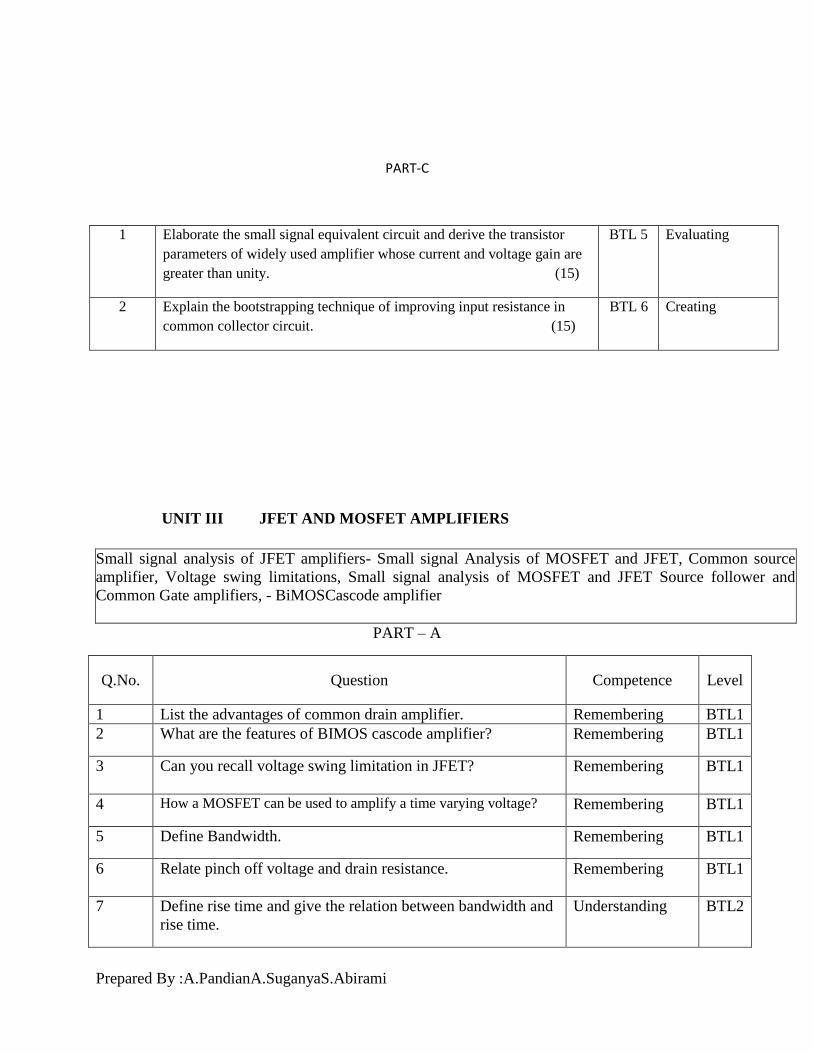
13. (i) For the circuit shown in figure, the transistor
parameters are ℎ𝑓𝑒 = 125, 𝑉𝐴 = ∞, 𝑉𝐶𝐶 = 18𝑉, 𝑅𝐿 =
4𝑘Ω, 𝑅𝐿 = 3𝑘Ω, 𝑅𝐶 = 4𝑘Ω, 𝑅1 =25.6𝑘Ω𝑎𝑛𝑑𝑅210.4𝑘Ω. the input signal is a current
Source. Measure its small signal voltage gain, current
gain, maximum voltage gain and input impedance
(8)
(ii) Assess the circuit diagram of bootstrapped emitter
follower with its equivalent circuit, derive for its input
and output impedance. (5)
BTL 5 Evaluating
14. (i) Design the small signal voltage gain of an emitter follower
circuit. Given 𝛽 = 100, 𝑉𝐵𝐸(𝑜𝑛) = 0.7𝑉, 𝑉𝐴 = 80𝑉, 𝐼𝐶𝑄 =
0.793𝑚𝐴, 𝑉𝐶𝐸𝑄 = 3.4𝑉. (7)
(ii) Discuss in detail about the operation of Darlington
amplifier. (6)
BTL 6 Creating
Prepared By :A.PandianA.SuganyaS.Abirami
PART-C
1 Elaborate the small signal equivalent circuit and derive the transistor
parameters of widely used amplifier whose current and voltage gain are
greater than unity. (15)
BTL 5 Evaluating
2 Explain the bootstrapping technique of improving input resistance in
common collector circuit. (15)
BTL 6 Creating
UNIT III JFET AND MOSFET AMPLIFIERS
Small signal analysis of JFET amplifiers- Small signal Analysis of MOSFET and JFET, Common source
amplifier, Voltage swing limitations, Small signal analysis of MOSFET and JFET Source follower and
Common Gate amplifiers, - BiMOSCascode amplifier
PART – A
Q.No. Question Competence Level
1 List the advantages of common drain amplifier. Remembering BTL1
2 What are the features of BIMOS cascode amplifier? Remembering BTL1
3 Can you recall voltage swing limitation in JFET?
Remembering BTL1
4 How a MOSFET can be used to amplify a time varying voltage? Remembering BTL1
5 Define Bandwidth. Remembering BTL1
6 Relate pinch off voltage and drain resistance.
Remembering BTL1
7 Define rise time and give the relation between bandwidth and
rise time.
Understanding BTL2
Prepared By :A.PandianA.SuganyaS.Abirami
8 Discuss the effect of bypass capacitor on bandwidth of the
amplifier.
Understanding BTL2
9 Two amplifiers having gain of 20 dB and 40 dB are cascaded.
Estimate the overall gain in dB.
Understanding BTL2
10 Distinguish between JFET and MOSFET amplifiers. Understanding BTL2
11 If the midband gain of an amplifier is 100 and half power
frequencies are fL =40Hz and fH=16kHz. Calculate the
amplifier gain at 20Hz and 20kHz frequency.
Applying BTL3
12 Illustrate about JFET common source amplifier. Applying BTL3
13 Construct a small signal model of JFET. Applying BTL3
14 The parameters for the transistor below are Kn= 0.5mA/V2,
VTN = 1.2V , and λ = 0. Simplify VDSandVGS for IQ=50 µA.
Analyzing BTL4
15 Analyze the output impedance for the MOSFET amplifier
given below. Provided: Kn= 1mA/V, VTN = 1.2V,λ = 0.01V−1,
Av= 0.855 and IDQ= 1mA.
Analyzing BTL4
16 Compare the three FET configurations (CS,CD and CG). Analyzing BTL4
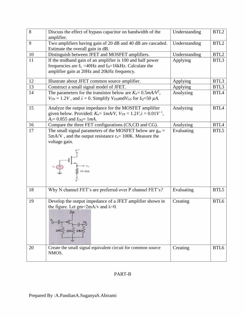
17 The small signal parameters of the MOSFET below are gm =
5mA/V , and the output resistance ro= 100K. Measure the
voltage gain.
Evaluating BTL5
18 Why N channel FET’s are preferred over P channel FET’s?
Evaluating BTL5
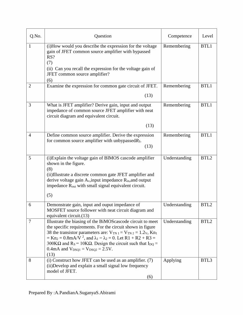
19 Develop the output impedance of a JFET amplifier shown in
the figure. Let gm=2mA/v and λ=0.
Creating BTL6
20 Create the small signal equivalent circuit for common source
NMOS.
Creating BTL6
PART-B
Prepared By :A.PandianA.SuganyaS.Abirami
Q.No. Question Competence Level
1 (i)How would you describe the expression for the voltage
gain of JFET common source amplifier with bypassed
RS?
(7)
(ii) Can you recall the expression for the voltage gain of
JFET common source amplifier?
(6)
Remembering BTL1
2 Examine the expression for common gate circuit of JFET.
(13)
Remembering BTL1
3 What is JFET amplifier? Derive gain, input and output
impedance of common source JFET amplifier with neat
circuit diagram and equivalent circuit.
(13)
Remembering BTL1
4 Define common source amplifier. Derive the expression
for common source amplifier with unbypassedRS.
(13)
Remembering BTL1
5 (i)Explain the voltage gain of BIMOS cascode amplifier
shown in the figure.
(8)
(ii)Illustrate a discrete common gate JFET amplifier and
derive voltage gain Av,input impedance Rin,and output
impedance Rout with small signal equivalent circuit.
(5)
Understanding BTL2
6 Demonstrate gain, input and ouput impedance of
MOSFET source follower with neat circuit diagram and
equivalent circuit.(13)
Understanding BTL2
7 Illustrate the biasing of the BiMOScascode circuit to meet
the specific requirements. For the circuit shown in figure
38 the transistor parameters are: VTN 1 = VTN 2 = 1.2V, Kn1
= Kn2 = 0.8mA/V 2, and λ1 = λ2 = 0. Let R1 + R2 + R3 =
300KΩ and RS = 10KΩ. Design the circuit such that IDQ =
0.4mA and VDSQ1 = VDSQ2 = 2.5V.
(13)
Understanding BTL2
8 (i) Construct how JFET can be used as an amplifier. (7)
(ii)Develop and explain a small signal low frequency
model of JFET.
(6)
Applying BTL3
Prepared By :A.PandianA.SuganyaS.Abirami
9 In a common gate configuration of MOSFET,
(i) Illustrate small signal voltage and current gain. (7) (8)
(ii) Examine input and output impedance. (6)
Applying BTL3
10 Analyze a simple JFET source-follower amplifier circuit
and discuss the general AC circuit characteristics. (13)
Analyzing BTL4
11 (i)Explain on voltage swing limitations, general
conditions under which a source follower amplifier would
be used. (10)
(ii) Examine and describe the characteristics of BiCMOS
circuits. (3)
Analyzing BTL4
12 (i) Pointout the small signal parameters of MOSFET.(7)
(ii) Select and configure a common-source amplifier with
source resistor. (6)
Analyzing BTL4
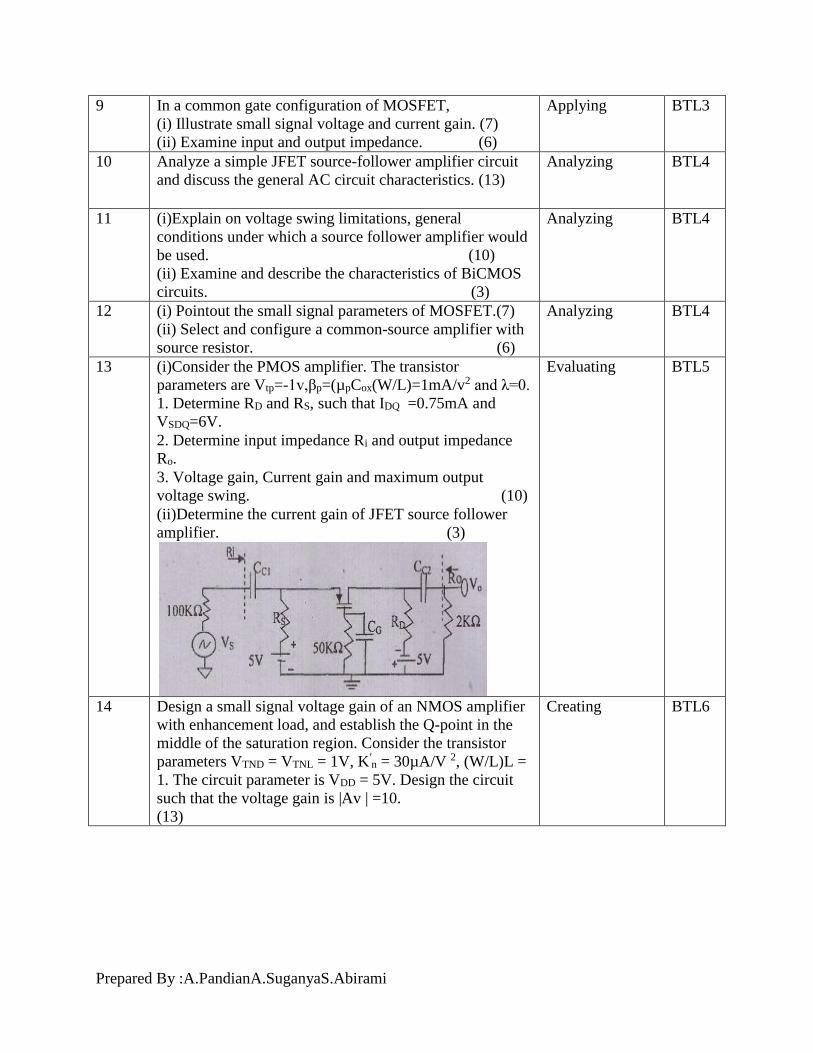
13 (i)Consider the PMOS amplifier. The transistor
parameters are Vtp=-1v,βp=(µpCox(W/L)=1mA/v2 and λ=0.
1. Determine RD and RS, such that IDQ =0.75mA and
VSDQ=6V.
2. Determine input impedance Ri and output impedance
Ro.
3. Voltage gain, Current gain and maximum output
voltage swing. (10)
(ii)Determine the current gain of JFET source follower
amplifier. (3)
Evaluating BTL5
14 Design a small signal voltage gain of an NMOS amplifier
with enhancement load, and establish the Q-point in the
middle of the saturation region. Consider the transistor
parameters VTND = VTNL = 1V, K′n = 30µA/V 2, (W/L)L =
1. The circuit parameter is VDD = 5V. Design the circuit
such that the voltage gain is |Av | =10.
(13)
Creating BTL6
Prepared By :A.PandianA.SuganyaS.Abirami
PART-C
1 Explain Voltage swing limitations and general conditions
under which a source amplifier would be used and explain
common source amplifier with source resistor and source
bypass capacitor. (15)
BTL5 Evaluating
2 Elaborate the characteristics of BiCMOScascode amplifier,
and explain graphically the amplification process in a simple
MOSFET amplifier circuit. (15)
BTL6 Creating
UNIT IV
FREQUENCY ANALYSIS OF BJT AND MOSFET AMPLIFIERS
Low frequency and Miller effect, High frequency analysis of CE and MOSFET CS amplifier, Short circuit current gain, cut off frequency – fα and fβ unity gain and Determination of bandwidth of single stage and multistage amplifiers
PART – A
Q.No. Question Competence Level
1 What is the effect of miller’s capacitance on the frequency
response of an amplifier?
Remembering BTL1
2 Define beta cutoff frequency. Remembering BTL1
3 List out the advantages of h parameter. Remembering BTL1
4 Can you recall the need of cascading multistage
amplifiers?
Remembering BTL1
5 Relate the term bandwidth and gain bandwidth product. Remembering BTL1
6 If the rise time of a BJT is 35 nano seconds. Identify the
bandwidth that can be obtained using this BJT ?
Remembering BTL1
7 Differentiate small signal equivalent & hybrid π
equivalent circuit.
Understanding BTL2
8 Express the equation of overall lower and upper cutoff
frequency of multistage amplifier.
Understanding BTL2
9 Give the main reason for the drop in gain at the low
frequency region & high frequency region.
Understanding BTL2
10 Discuss the limitations of multistage amplifiers. Understanding BTL2
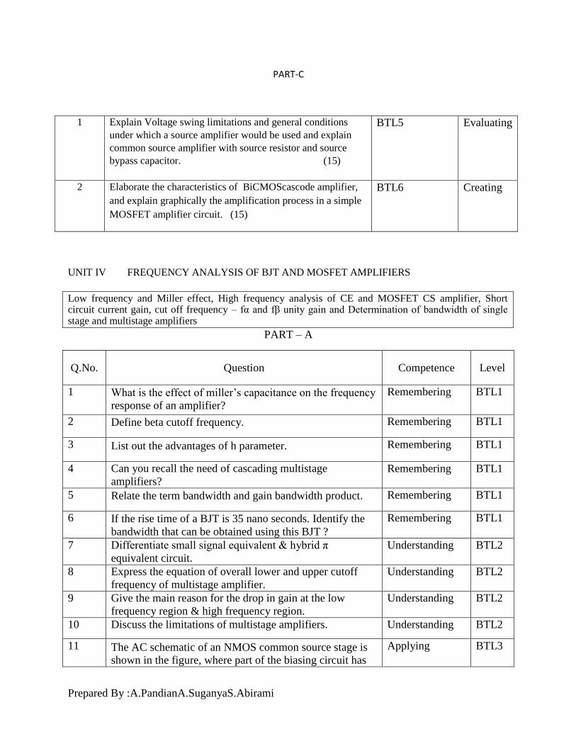
11 The AC schematic of an NMOS common source stage is
shown in the figure, where part of the biasing circuit has
Applying BTL3
Prepared By :A.PandianA.SuganyaS.Abirami
been omitted for simplicity. For the N-channel MOSFET
M1,thetransconductance, gm=1mA/v and body effect and
channel length modulation effect are to be neglected.
Identify the lower cutoff frequency.
12 Develop and explain about Miller Impedance. Applying BTL3
13 Solve the unity gain bandwidth of MOSFET whose gm =
6m A/V, Cgs = 8pF, Cgd= 4 pF, and Cds = 1 pF.
Applying BTL3
14 Compare BJT and MOSFET Amplifiers. Analyzing BTL4
15 Short circuit CE current gain of transistor is 25 at a
frequency of 2 MHz if fᵦ = 200 KHz Examine i) = 200
KHz ii) hfe iii) find |Ai| at frequency of 10 MHz and 100
MHz.
Analyzing BTL4
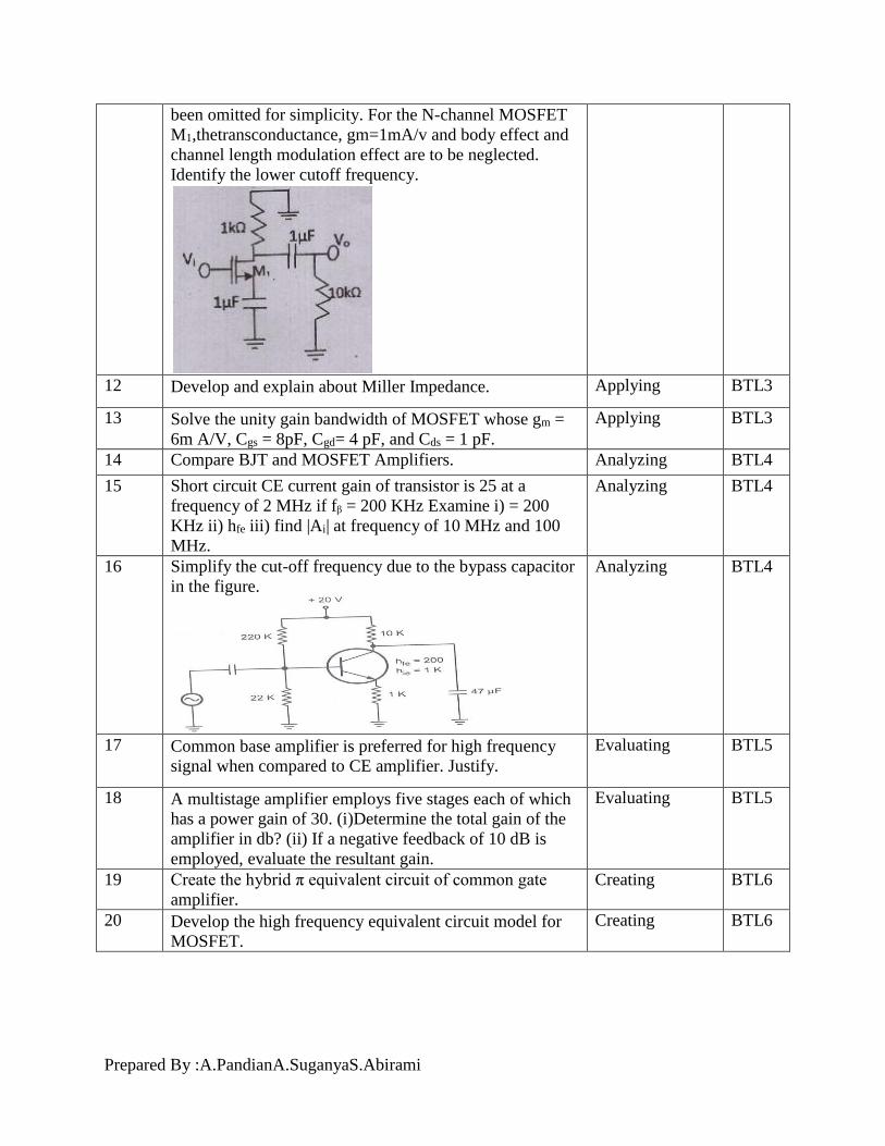
16 Simplify the cut-off frequency due to the bypass capacitor
in the figure.
Analyzing BTL4
17 Common base amplifier is preferred for high frequency
signal when compared to CE amplifier. Justify.
Evaluating BTL5
18 A multistage amplifier employs five stages each of which
has a power gain of 30. (i)Determine the total gain of the
amplifier in db? (ii) If a negative feedback of 10 dB is
employed, evaluate the resultant gain.
Evaluating BTL5
19 Create the hybrid π equivalent circuit of common gate
amplifier.
Creating BTL6
20 Develop the high frequency equivalent circuit model for
MOSFET.
Creating BTL6
Prepared By :A.PandianA.SuganyaS.Abirami
PART-B
Q.No. Question Competence Level
1 Describe in detail with neat diagram frequency response of
BJT amplifier. Discuss the significance of cut off
frequencies and bandwidth of the amplifier. (13)
Remembering BTL1
2 Examine the upper and lower cut off frequencies of
multistage amplifier with expressions. (13)
Remembering BTL1
3 How would you describe the relation between rise time,
upper cut off frequency and bandwidth? (13)
Remembering BTL1
4 Can you recall the operation of high frequency common
source FET amplifier with neat diagram? Derive the
expression for i) Voltage gain ii) Input admittance iii) input
capacitance iv) Output admittance. (13)
Remembering BTL1
5 For the circuit shown in the fig. Illustrate cut-off
frequencies due to C1,C2,Cs due to interelectrode capacitors
Cgs and Cgd, gm=0.49mA/v,Cgd=9.38pF,Cgs=1.8pF,rd=40
KΩ. (13)
Understanding BTL2
6 (i)Discuss in detail about the bandwidth of single stage
amplifiers.(7)
(ii) Describe in detail about gain bandwidth product for
voltage and current of BJT. (6)
Understanding BTL2
7 (i)Estimate the bandwidth of CE amplifier with the
following specifications. R1=100kΩ, R2=10kΩ, RC=9kΩ,
RE=2kΩ, C1= C2=25μF, CE=50μF, rbb’=100Ω, rb’e=1.1KΩ,
hfe=225,
Cb’e=3pF and Cb’c=100pF. (7)
(ii) Summarize the expression for Low Frequency Analysis
of BJT. (6)
Understanding BTL2
8 (i)Write a brief outline about multistage amplifiers.(8)
(ii)Examine the advantages and applications of single stage
and multistage amplifiers. (5)
Applying BTL3
Prepared By :A.PandianA.SuganyaS.Abirami
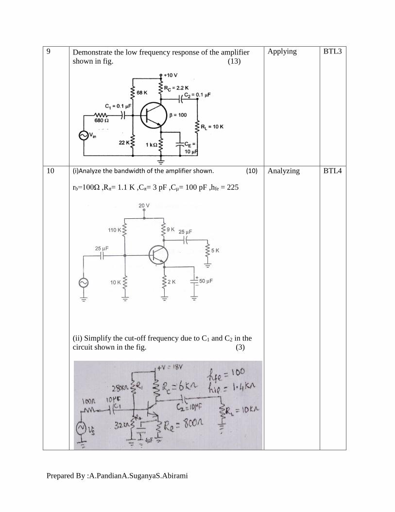
9 Demonstrate the low frequency response of the amplifier
shown in fig. (13)
Applying BTL3
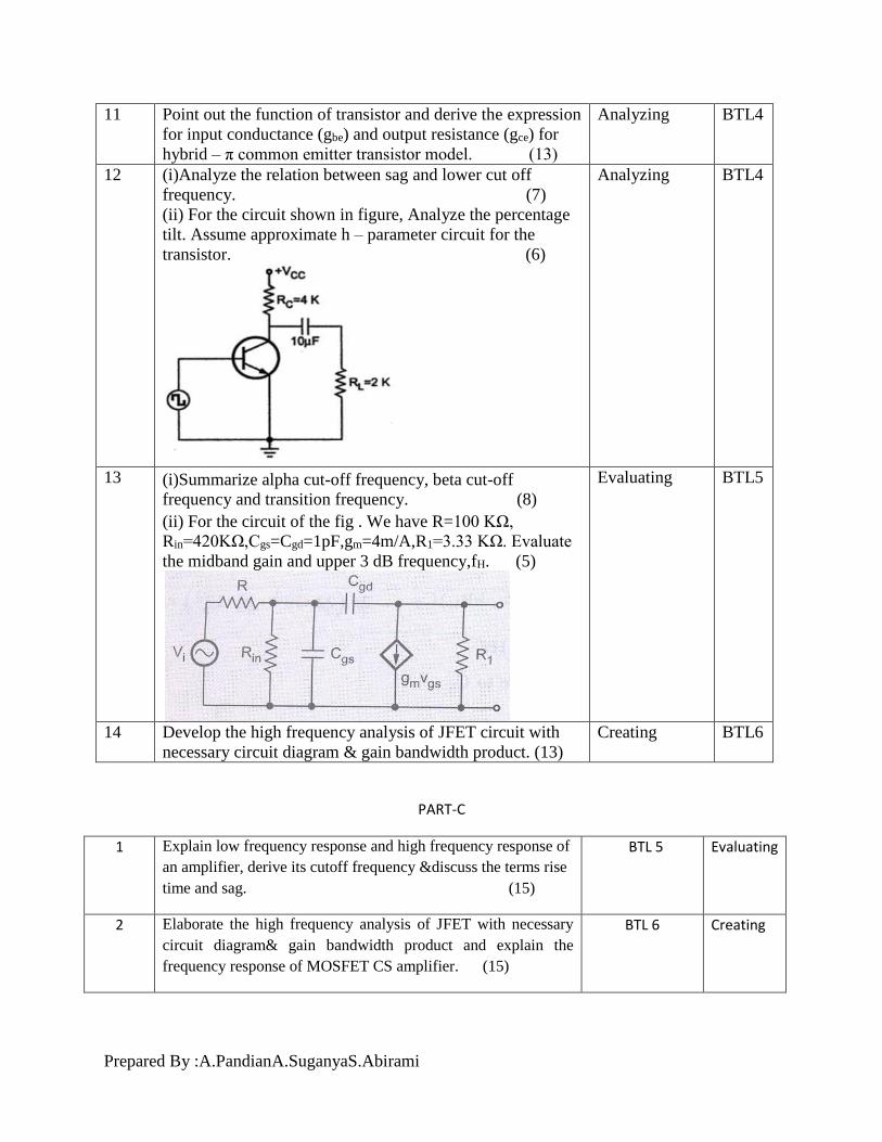
10 (i)Analyze the bandwidth of the amplifier shown. (10)
rb=100Ω ,Rπ= 1.1 K ,Cπ= 3 pF ,Cµ= 100 pF ,hfe = 225
(ii) Simplify the cut-off frequency due to C1 and C2 in the
circuit shown in the fig. (3)
Analyzing BTL4
Prepared By :A.PandianA.SuganyaS.Abirami
11 Point out the function of transistor and derive the expression
for input conductance (gbe) and output resistance (gce) for
hybrid – π common emitter transistor model. (13)
Analyzing BTL4
12 (i)Analyze the relation between sag and lower cut off
frequency. (7)
(ii) For the circuit shown in figure, Analyze the percentage
tilt. Assume approximate h – parameter circuit for the
transistor. (6)
Analyzing BTL4
13 (i)Summarize alpha cut-off frequency, beta cut-off
frequency and transition frequency. (8)
(ii) For the circuit of the fig . We have R=100 KΩ,
Rin=420KΩ,Cgs=Cgd=1pF,gm=4m/A,R1=3.33 KΩ. Evaluate
the midband gain and upper 3 dB frequency,fH. (5)
Evaluating BTL5
14 Develop the high frequency analysis of JFET circuit with
necessary circuit diagram & gain bandwidth product. (13)
Creating BTL6
PART-C
1 Explain low frequency response and high frequency response of
an amplifier, derive its cutoff frequency &discuss the terms rise
time and sag. (15)
BTL 5 Evaluating
2 Elaborate the high frequency analysis of JFET with necessary
circuit diagram& gain bandwidth product and explain the
frequency response of MOSFET CS amplifier. (15)
BTL 6 Creating

Prepared By :A.PandianA.SuganyaS.Abirami
UNIT- IC MOSFET AMPLIFIERS
IC Amplifiers- IC biasing Current steering circuit using MOSFET- MOSFET current sources- PMOS and NMOS current sources. Amplifier with active loads - enhancement load, Depletion load and PMOS and NMOS current sources load- CMOS common source and source follower- CMOS differential amplifier- CMRR.
PART- A
Q.No Questions BT
Level
Competence
1. What is the common mode rejection ratio? BTL 1 Remembering
2. Define MOSFET load devices amplifiers? BTL 1 Remembering
3. Name two type of transistor current source? BTL 1 Remembering
4. How would you explain the saturation and non- saturation bias regions?. BTL 1 Remembering
5. Can you recall the advantage of Wilson current mirror circuit? BTL 1 Remembering
6. Summarize the advantages of an active load. BTL 1 Remembering
7. Outline about thecascode current mirror. BTL 2 Understand
8. Illustrate the various types of active loads. BTL 2 Understand
9. Demonstrate the MOSFET is biased in the saturation region. BTL 2 Understand
10. Contrast Wilson current source. BTL 2 Understand
11. Identify the limitation of the NMOS amplifier with depletion load? BTL 3 Apply
12. Develop the NMOS depletion load amplifier parameter. BTL 3 Apply
13. Model the gm of CMOS differential amplifier in large signal equivalent circuit? BTL 3 Apply
14. Analyze the matched transistors load in CMOS amplifier.. BTL 4 Analyze
15. Categorize need for MOSFET differential amplifier with cascode active load. BTL 4 Analyze
16. Contrast the operation of transistor in voltage transfer characteristics of CMOS
common source amplifier.
BTL 4 Analyze
17. Assess opinion of active load MOSFET. BTL 5 Evaluate
18. Evaluate the output current in current steering circuit. BTL 5 Evaluate
19. Discuss the enhancement and depletion mode of MOSFET. BTL 6 Create
Prepared By :A.PandianA.SuganyaS.Abirami
20. Elaborate on MOSFET cascode current source circuit. BTL 6 Create
PART –B
1. (i)Define current source and explain basic MOSFET current source with suitable
diagrams? (10)
(ii)Label the effect of Vo and Io. (3)
BTL 1 Remembering
2. How to made DC bias current in MOSFET current Steering circuit and explain
withsuitable diagram. (13)
BTL 1 Remembering
3. Define current mirror circuit and explain following
(i) Cascode current mirror (7)
(ii) Wilson current mirror. (6)
BTL 1 Remembering
4. Why current steering circuit required in MOSFET Amplifier and Explain the
operation with a circuit diagram? (13)
BTL 1 Remembering
5. (i) Outline the voltage transfer characteristics MOSFET amplifier with gate and
drain shorted load. (7)
(ii) Summarize the voltage transfer characteristics NMOS amplifier with
enhancement load. (6)
BTL
2
Understand
6. (i)Illustrate the NMOS inverter with depletion load amplifier. (10)
(ii) Contrast the PMOS with enhancement load. (3)
BTL
2
Understand
7. (i) summarize the NMOS CS amplifier?and Explain the operation with a circuit
diagram. (10)
(ii)State the advantages of CMOS common-source amplifier. (3)
BTL
2
Understand
8. (i)Develop current mirror circuit in CMOS differential amplifier (8)
(i) Model the equivalent circuit and drive expression for Ad, Acm and CMMR for
CMOS differential amplifier. (5)
BTL
3
Apply
9. Examine the MOSFET cascade current source, all transistor are identical and
transistor circuit parameters are as follows: Vt=1V,Kn=40uA/v2,
λ=0.02v-1,iref=10uA and VDD=10V.find:a)VGS of each MOSFET. (5)
b)The lowest possible voltage value VD4,the output resistance Ro. . (8)
BTL 4 Analyze
10. Inspect the parameter in MOSFET current source amplifier for the following
specifications: VDD = +5V, Kn’ = 40 µA/V2, VT = 1V, λ = 0, IREF = 0.2mA, I0 =
0.1mA and VDS2(sat) = 0.8V. (13)
BTL 4 Analyze
11. Simplify the parameter in NMOS amplifier with depletion load, VTN1 = 0.8V, VTN2
= - 1.0V, Kn1 = 2mA/V2, Kn2 = 0.2mA/V2, IDQ = 0.2mA, λ1= λ2 = 0.01V-1. Calculate
the small signal voltage gain. (13)
BTL 4 Analyze
12. (i)Builda CMOS common source amplifier and explain the with the help of various
characteristics.(10)
(ii)Model the CMOS common-source
amplifier,Kn”=80uA/v2.kp=20uA/V2,Vtn=0.8V,
Vtp=-1V,(W/L)n=10,(W/L)P=20,Ibias=0.2mA and λ1=λ2=0.0101V-1,find the small-
BTL
3
Apply

Prepared By :A.PandianA.SuganyaS.Abirami
signal voltage gain.(3)
13. (i) Explain the CMOS differential amplifier with Enhancement active load.(10)
(ii) Assess the advantages of CMOS differential amplifier with current mirror load.
(3)
BTL
5
Evaluate
14. Design a NMOS amplifier with depletion load ,Vtn1=.8v,
Vtn2=-1V,Kn1=2mA/V2,Kn2=0.2mA/v2,IDq=0.2mA and λ1=λ2=0.01V-1,calculate
the small-signal voltage gain.(13)
BTL
6
Create
PART-C
1 Conclude the Input and Output Currents, Input and Output Impedances and
Frequency Response, Advantages, Limitation of current mirror and Wilson current
mirror circuit . (15)
BTL 5 Evaluating
2 Construct a MOSFET current source amplifier for the following specifications:
VDD = +5V, Kn’ = 40 µA/V2, VT = 1V, λ = 0, IREF = 0.2mA, I0 = 0.1mA and
VDS2(sat) = 0.8V. (15)
BTL 6 Creating