Embed Size (px)
Citation preview

V9261F Datasheet
Copyright © 2016 Vango Technologies, Inc.
This document contains information that is proprietary to Vango Technologies, Inc.
Unauthorized reproduction of this information in whole or in part is strictly prohibited.
V9261F DATASHEET
Single-Phase Energy Metering AFE
i
Vango Technologies, Inc.
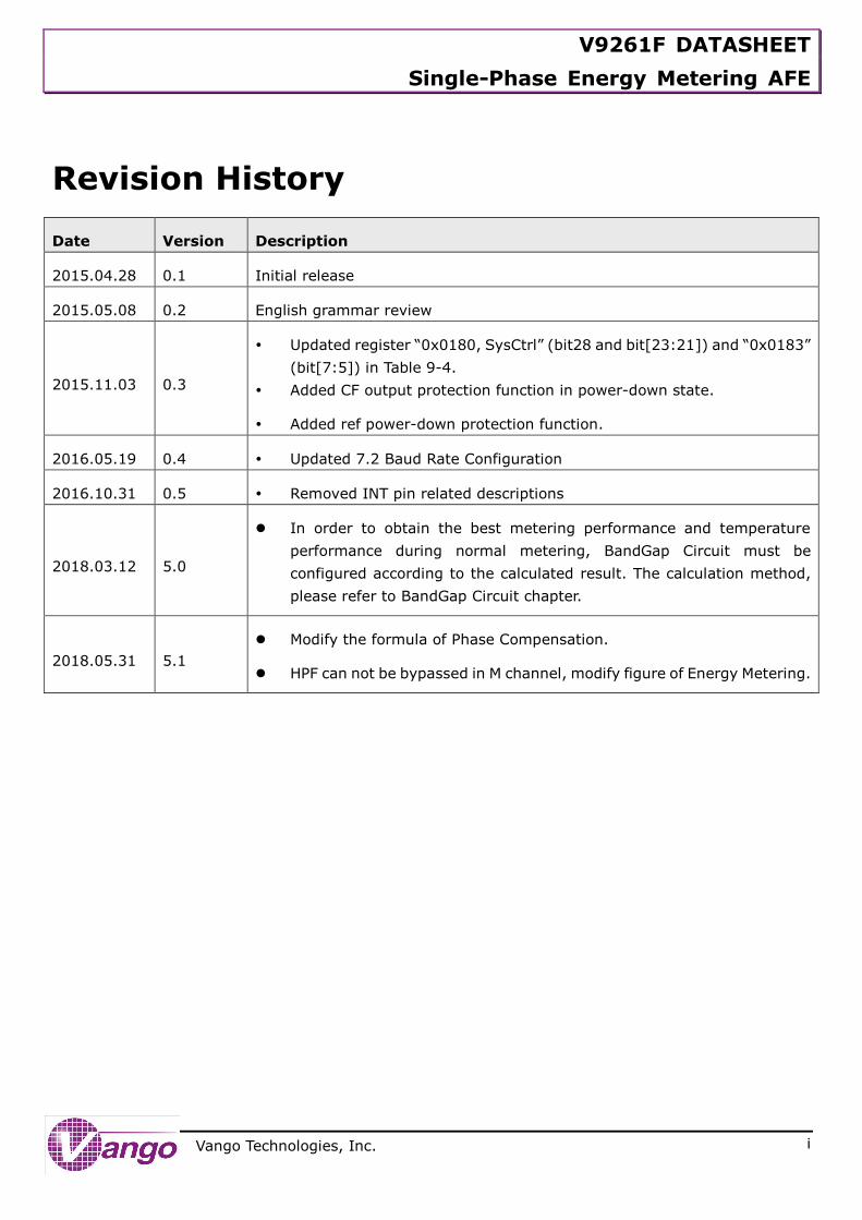
Revision History
Date Version Description
2015.04.28 0.1 Initial release
2015.05.08 0.2 English grammar review
2015.11.03 0.3
Updated register “0x0180, SysCtrl” (bit28 and bit[23:21]) and “0x0183”
(bit[7:5]) in Table 9-4.
Added CF output protection function in power-down state.
Added ref power-down protection function.
2016.05.19 0.4 Updated 7.2 Baud Rate Configuration
2016.10.31 0.5 Removed INT pin related descriptions
2018.03.12 5.0
In order to obtain the best metering performance and temperature
performance during normal metering, BandGap Circuit must be
configured according to the calculated result. The calculation method,
please refer to BandGap Circuit chapter.
2018.05.31 5.1
Modify the formula of Phase Compensation.
HPF can not be bypassed in M channel, modify figure of Energy Metering.
V9261F DATASHEET
Single-Phase Energy Metering AFE
ii
Vango Technologies, Inc.
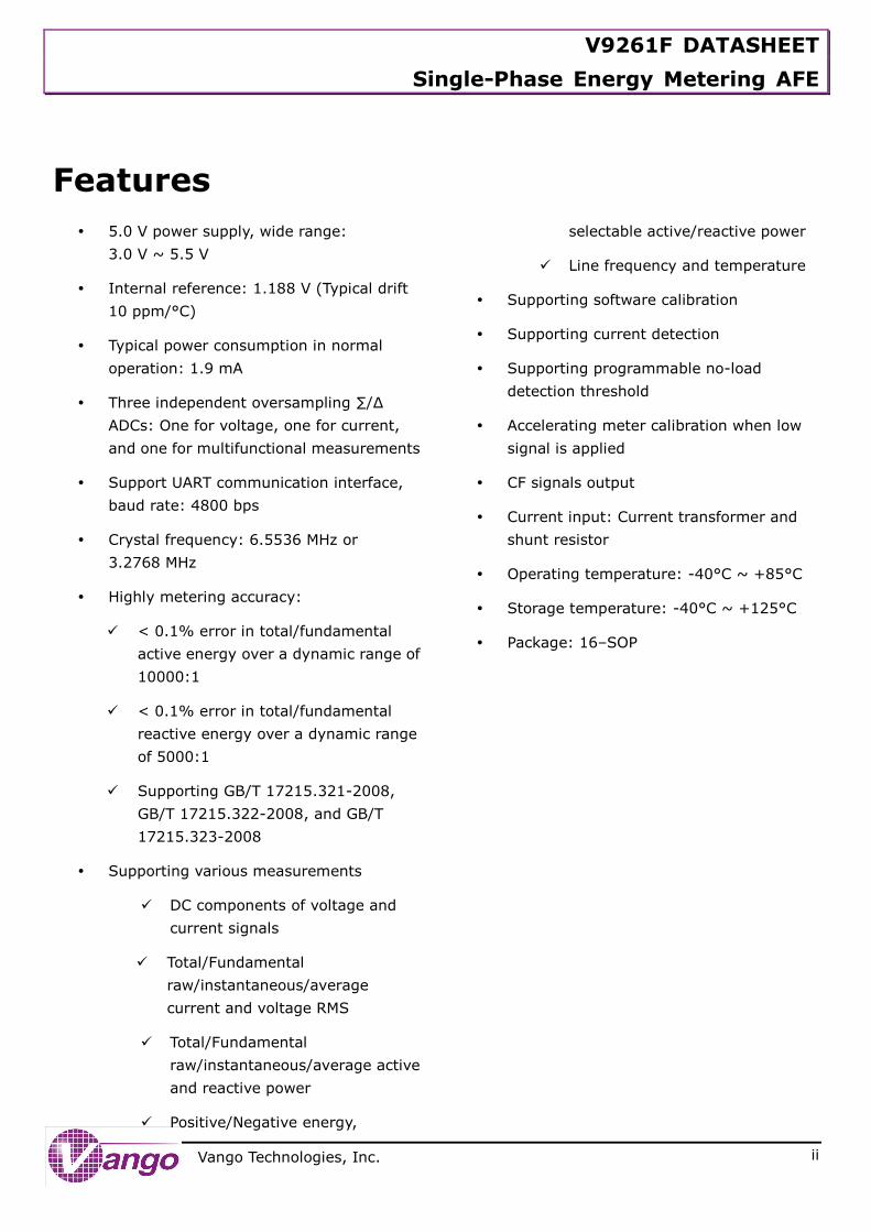
Features
5.0 V power supply, wide range:
3.0 V ~ 5.5 V
Internal reference: 1.188 V (Typical drift
10 ppm/°C)
Typical power consumption in normal
operation: 1.9 mA
Three independent oversampling ∑/∆
ADCs: One for voltage, one for current,
and one for multifunctional measurements
Support UART communication interface,
baud rate: 4800 bps
Crystal frequency: 6.5536 MHz or
3.2768 MHz
Highly metering accuracy:
< 0.1% error in total/fundamental
active energy over a dynamic range of
10000:1
< 0.1% error in total/fundamental
reactive energy over a dynamic range
of 5000:1
Supporting GB/T 17215.321-2008,
GB/T 17215.322-2008, and GB/T
17215.323-2008
Supporting various measurements
DC components of voltage and
current signals
Total/Fundamental
raw/instantaneous/average
current and voltage RMS
Total/Fundamental
raw/instantaneous/average active
and reactive power
Positive/Negative energy,
selectable active/reactive power
Line frequency and temperature
Supporting software calibration
Supporting current detection
Supporting programmable no-load
detection threshold
Accelerating meter calibration when low
signal is applied
CF signals output
Current input: Current transformer and
shunt resistor
Operating temperature: -40°C ~ +85°C
Storage temperature: -40°C ~ +125°C
Package: 16–SOP
V9261F DATASHEET
Single-Phase Energy Metering AFE
Vango Technologies, Inc.
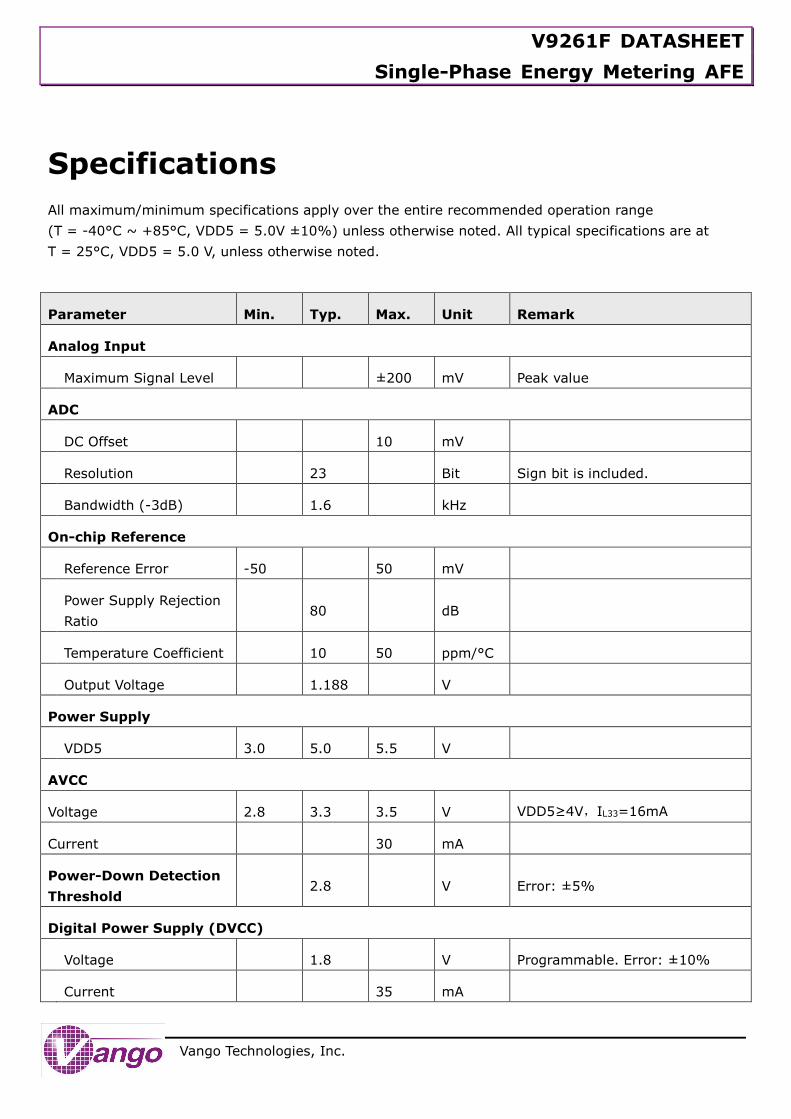
Specifications
All maximum/minimum specifications apply over the entire recommended operation range
(T = -40°C ~ +85°C, VDD5 = 5.0V ±10%) unless otherwise noted. All typical specifications are at
T = 25°C, VDD5 = 5.0 V, unless otherwise noted.
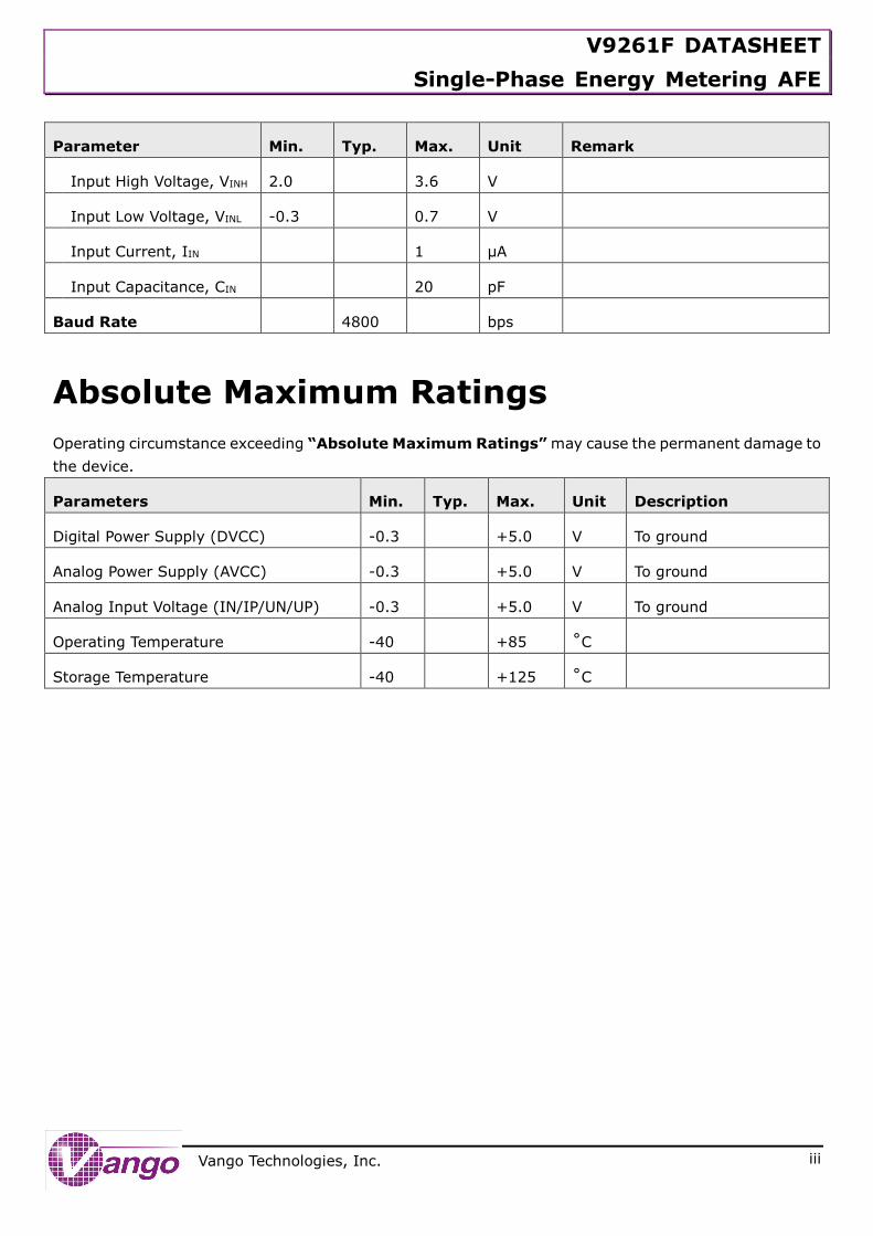
Parameter Min. Typ. Max. Unit Remark
Analog Input
Maximum Signal Level ±200 mV Peak value
ADC
DC Offset 10 mV
Resolution 23 Bit Sign bit is included.
Bandwidth (-3dB) 1.6 kHz
On-chip Reference
Reference Error -50 50 mV
Power Supply Rejection
Ratio 80 dB
Temperature Coefficient 10 50 ppm/°C
Output Voltage 1.188 V
Power Supply
VDD5 3.0 5.0 5.5 V
AVCC
Voltage 2.8 3.3 3.5 V VDD5≥4V,IL33=16mA
Current 30 mA
Power-Down Detection
Threshold 2.8 V Error: ±5%
Digital Power Supply (DVCC)
Voltage 1.8 V Programmable. Error: ±10%
Current 35 mA
V9261F DATASHEET
Single-Phase Energy Metering AFE
i
Vango Technologies, Inc.
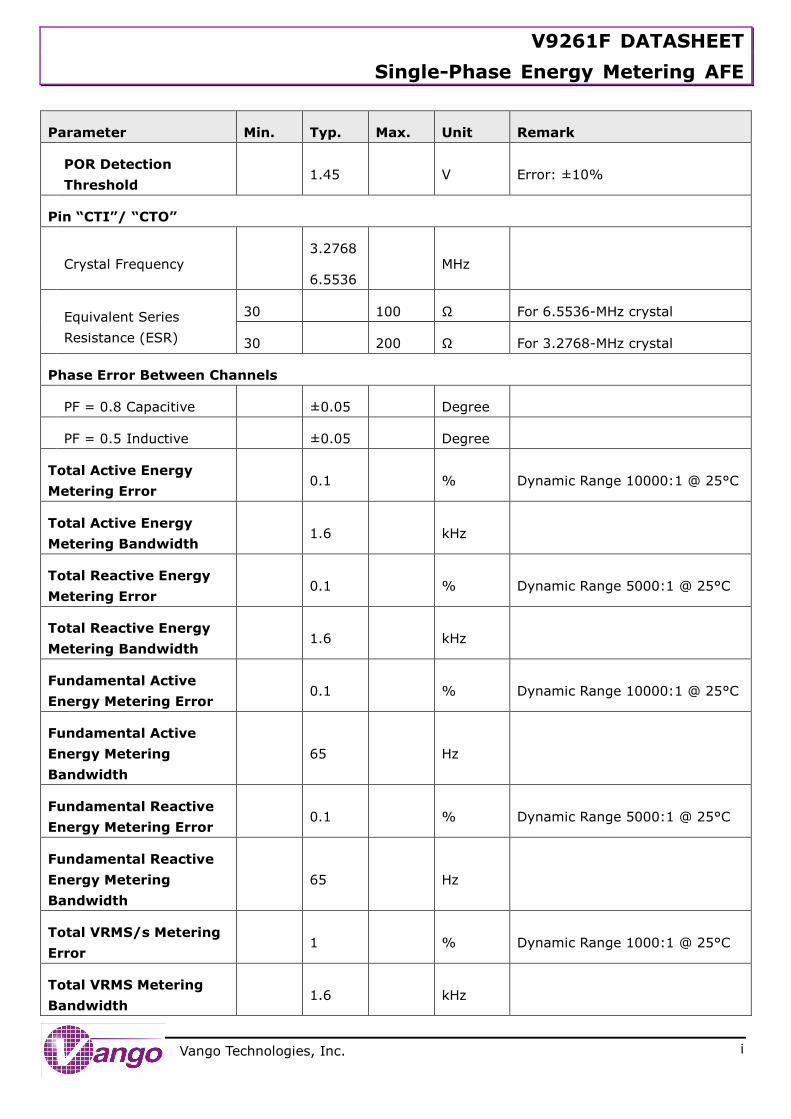
Parameter Min. Typ. Max. Unit Remark
POR Detection
Threshold 1.45 V Error: ±10%
Pin “CTI”/ “CTO”
Crystal Frequency 3.2768
6.5536 MHz
Equivalent Series
Resistance (ESR)
30 100 Ω For 6.5536-MHz crystal
30 200 Ω For 3.2768-MHz crystal
Phase Error Between Channels
PF = 0.8 Capacitive ±0.05 Degree
PF = 0.5 Inductive ±0.05 Degree
Total Active Energy
Metering Error 0.1 % Dynamic Range 10000:1 @ 25°C
Total Active Energy
Metering Bandwidth 1.6 kHz
Total Reactive Energy
Metering Error 0.1 % Dynamic Range 5000:1 @ 25°C
Total Reactive Energy
Metering Bandwidth 1.6 kHz
Fundamental Active
Energy Metering Error 0.1 % Dynamic Range 10000:1 @ 25°C
Fundamental Active
Energy Metering
Bandwidth
65 Hz
Fundamental Reactive
Energy Metering Error 0.1 % Dynamic Range 5000:1 @ 25°C
Fundamental Reactive
Energy Metering
Bandwidth
65 Hz
Total VRMS/s Metering
Error 1 % Dynamic Range 1000:1 @ 25°C
Total VRMS Metering
Bandwidth 1.6 kHz
V9261F DATASHEET
Single-Phase Energy Metering AFE
ii
Vango Technologies, Inc.
Parameter Min. Typ. Max. Unit Remark
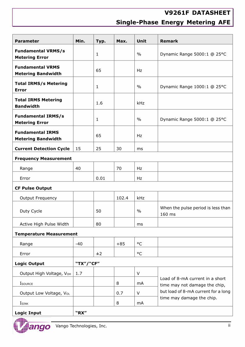
Fundamental VRMS/s
Metering Error 1 % Dynamic Range 5000:1 @ 25°C
Fundamental VRMS
Metering Bandwidth 65 Hz
Total IRMS/s Metering
Error 1 % Dynamic Range 1000:1 @ 25°C
Total IRMS Metering
Bandwidth 1.6 kHz
Fundamental IRMS/s
Metering Error 1 % Dynamic Range 5000:1 @ 25°C
Fundamental IRMS
Metering Bandwidth 65 Hz
Current Detection Cycle 15 25 30 ms
Frequency Measurement
Range 40 70 Hz
Error 0.01 Hz
CF Pulse Output
Output Frequency 102.4 kHz
Duty Cycle 50 % When the pulse period is less than
160 ms
Active High Pulse Width 80 ms
Temperature Measurement
Range -40 +85 °C
Error ±2 °C
Logic Output “TX”/“CF”
Output High Voltage, VOH 1.7 V
Load of 8-mA current in a short
time may not damage the chip,
but load of 8-mA current for a long
time may damage the chip.
ISOURCE 8 mA
Output Low Voltage, VOL 0.7 V
ISINK 8 mA
Logic Input “RX”
V9261F DATASHEET
Single-Phase Energy Metering AFE
iii
Vango Technologies, Inc.
Parameter Min. Typ. Max. Unit Remark
Input High Voltage, VINH 2.0 3.6 V
Input Low Voltage, VINL -0.3 0.7 V
Input Current, IIN 1 μA
Input Capacitance, CIN 20 pF
Baud Rate 4800 bps
Absolute Maximum Ratings
Operating circumstance exceeding “Absolute Maximum Ratings” may cause the permanent damage to
the device.
Parameters Min. Typ. Max. Unit Description
Digital Power Supply (DVCC) -0.3 +5.0 V To ground
Analog Power Supply (AVCC) -0.3 +5.0 V To ground
Analog Input Voltage (IN/IP/UN/UP) -0.3 +5.0 V To ground
Operating Temperature -40 +85 ˚C
Storage Temperature -40 +125 ˚C
V9261F DATASHEET
Single-Phase Energy Metering AFE
iv
Vango Technologies, Inc.
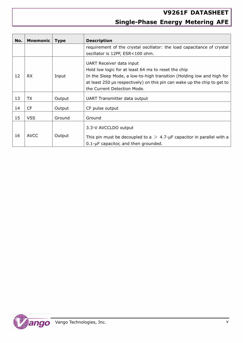
Pin Descriptions
1 2 3 4 5 6 7 8
16 15 14 13 12 11 10 9
AVCC
VD
D5
UP
UN
IAN
IAP
REF
DVCC
CTI
TX
RX
CF
VSS
V9261FIB
N
IBP
CTO
No. Mnemonic Type Description
1 VDD5 Power 5.0-V power supply
This pin must be decoupled to a ≥0.1-μF capacitor.
2 UP Input Positive input for Voltage Channel
3 UN Input Negative input for Voltage Channel
4 IBN Input Negative input for Current Channel B (IB)
5 IBP Input Positive input for Current Channel B (IB)
6 IAN Input Negative input for Current Channel A (IA)
7 IAP Input Positive input for Current Channel A (IA)
8 REF Input/Output
On-chip reference
This pin must be connected to a 1-μF capacitor, and then analog
grounded.
9 DVCC Power
Digital power output
This pin must be connected to a parallel circuit combined by a ≥
4.7-μF capacitor and 0.1-μF capacitor, and then grounded.
10 CTI Input Connect a 6.5536-MHz crystal around both pins.
There is fixed load capacitance of 12 pF in the oscillation circuit. The 11 CTO Output
V9261F DATASHEET
Single-Phase Energy Metering AFE
v
Vango Technologies, Inc.
No. Mnemonic Type Description
requirement of the crystal oscillator: the load capacitance of crystal
oscillator is 12PF, ESR<100 ohm.
12 RX Input
UART Receiver data input
Hold low logic for at least 64 ms to reset the chip
In the Sleep Mode, a low-to-high transition (Holding low and high for
at least 250 μs respectively) on this pin can wake up the chip to get to
the Current Detection Mode.
13 TX Output UART Transmitter data output
14 CF Output CF pulse output
15 VSS Ground Ground
16 AVCC Output
3.3-V AVCCLDO output
This pin must be decoupled to a ≥ 4.7-μF capacitor in parallel with a
0.1-μF capacitor, and then grounded.
V9261F DATASHEET
Single-Phase Energy Metering AFE
vi
Vango Technologies, Inc.
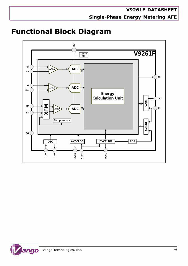
Functional Block Diagram
V9261F
APGA
1.188V REF
DVCCLDO POR
UA
RT
SysC
trl
OSC
APGA
APGA
Energy Calculation Unit
UP
UN
IAP
IAN
IBP
IBN
VSS
DV
CC
AV
CC
RX
TX
CT
I
CT
O
CF
REF
MU
X
ADC
U
I
M
Temp. sensor
ADC
ADC
AVCCLDO
VD
D5
V9261F DATASHEET
Single-Phase Energy Metering AFE
- 1 -
Vango Technologies, Inc.
Table of Contents
Revision History ...................................................................................................................... i
Features ................................................................................................................................. ii
Specifications ...........................................................................................................................
Absolute Maximum Ratings ................................................................................................... iii
Pin Descriptions .................................................................................................................... iv
Functional Block Diagram ...................................................................................................... vi
Table of Contents ................................................................................................................... 1
Figure List .............................................................................................................................. 3
Table List ............................................................................................................................... 4
1. Reset ............................................................................................................................. 6
1.1. Power-On Reset (POR) ................................................................................................ 6
1.2. RX Reset ................................................................................................................... 7
1.3. Global Software Reset ................................................................................................. 7
1.4. Registers ................................................................................................................... 8
2. Clock ............................................................................................................................. 9
2.1. Crystal Oscillation Circuit ............................................................................................. 9
2.2. 3.2-MHz RC Oscillator ............................................................................................... 10
2.3. 32-kHz RC Oscillator ................................................................................................. 11
2.4. Registers ................................................................................................................. 12
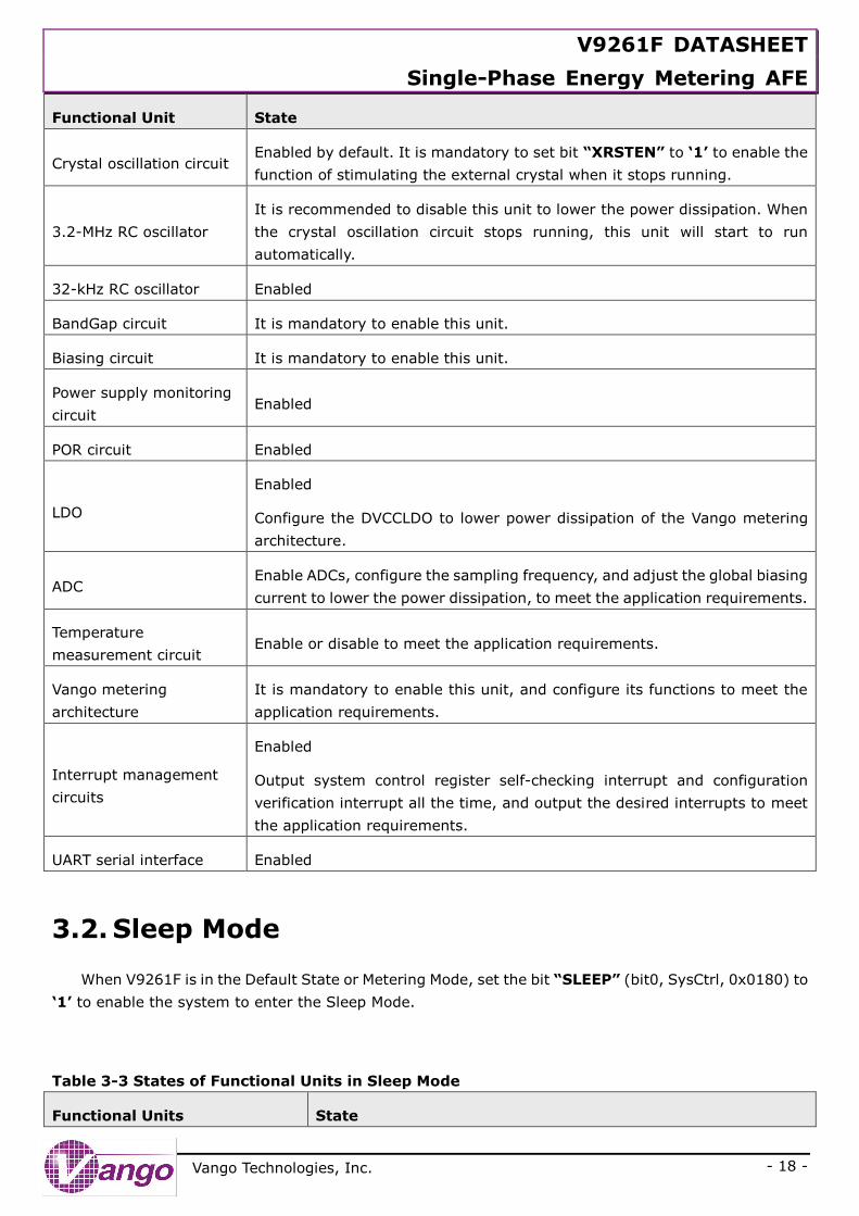
3. Operation Modes ......................................................................................................... 16
3.1. Metering Mode ......................................................................................................... 17
3.2. Sleep Mode .............................................................................................................. 18
3.3. Current Detection Mode ............................................................................................. 19
3.4. Power Dissipation ..................................................................................................... 21
4. Power Supply .............................................................................................................. 24
4.1. Power Supply Monitoring Circuit ................................................................................. 24
4.2. Digital Power Supply ................................................................................................. 25
4.3. Registers ................................................................................................................. 25
5. BandGap Circuit ........................................................................................................... 27
6. Energy Metering .......................................................................................................... 29
6.1. Metering Clock (“MEACLK”) ........................................................................................ 31
6.2. Analog Input ............................................................................................................ 31
6.3. Analog-to-Digital Conversion ...................................................................................... 33
V9261F DATASHEET
Single-Phase Energy Metering AFE
- 2 -
Vango Technologies, Inc.
6.4. Phase Compensation ................................................................................................. 35
6.5. Digital Input and DC Removement .............................................................................. 36
6.6. RMS Calculation ....................................................................................................... 38
6.7. Power Calculation ..................................................................................................... 39
6.8. Energy Accumulation and CF Pulse Output ................................................................... 41
6.9. No-Load Detection .................................................................................................... 44
6.10. Line Frequency Measurement .................................................................................. 44
6.11. Measuring Various Signals in M Channel ................................................................... 45
6.12. Calibration ............................................................................................................ 48
6.12.1. Registers for Meter Calibration ......................................................................... 48
6.12.2. Equations for Calibration ................................................................................. 50
6.12.3. Calibration Steps ............................................................................................ 52
7. UART Interface ............................................................................................................ 54
7.1. Data Byte ................................................................................................................ 54
7.2. Baud Rate Configuration ............................................................................................ 54
7.3. Communication Protocol ............................................................................................ 54
7.3.1. Write Operation ............................................................................................... 56
7.3.2. Read Operation ................................................................................................ 57
7.3.3. Broadcast Communication ................................................................................. 58
8. Interrupt ..................................................................................................................... 60
8.1. System Control Register Self-Checking Interrupt .......................................................... 60
8.2. Configuration Verification Interrupt ............................................................................. 60
8.3. Zero-Crossing Interrupt ............................................................................................. 62
8.4. Current Detection Interrupt ....................................................................................... 62
8.5. Registers ................................................................................................................. 64
9. Registers ..................................................................................................................... 66
9.1. Analog Control Registers............................................................................................ 66
9.2. System Control Register ............................................................................................ 72
9.3. Metering Control Registers ......................................................................................... 76
9.4. Data Registers.......................................................................................................... 81
9.5. Registers for Calibration ............................................................................................ 89
9.6. Checksum Register ................................................................................................... 92
10. Outline Dimensions ..................................................................................................... 93
V9261F DATASHEET
Single-Phase Energy Metering AFE
- 3 -
Vango Technologies, Inc.
Figure List
Figure 1-1 Timing of POR ............................................................................................................................................. 6
Figure 1-2 Timing of RX Reset ................................................................................................................................... 7
Figure 1-3 Timing of Global Software Reset ....................................................................................................... 8
Figure 2-1 Clock Generation ....................................................................................................................................... 9
Figure 3-1 Operating Modes...................................................................................................................................... 17
Figure 4-1 Power Supply Architecture ................................................................................................................. 24
Figure 4-2 Power-Down Interrupt ......................................................................................................................... 25
Figure 6-1 Signal Processing in Vango Metering Architecture ................................................................ 30
Figure 6-2 Analog Input of Current Channels .................................................................................................. 31
Figure 6-3 Analog Input of Voltage Channels .................................................................................................. 32
Figure 6-4 Channel Selection for Current Signal Processing .................................................................... 34
Figure 6-5 Phase Compensation ............................................................................................................................. 35
Figure 6-6 Digital Input and DC Removement (Current Signal is Taken as an Example.) ........ 36
Figure 6-7 Total / Fundamental RMS Calculation .......................................................................................... 39
Figure 6-8 Active/Reactive Power Calculation ................................................................................................ 40
Figure 6-9 Energy Accumulation and CF Pulse Output ................................................................................ 42
Figure 6-10 Signal Processing in M Channel ..................................................................................................... 46
Figure 7-1 Structure of an 11-Bit Data Byte ..................................................................................................... 54
Figure 7-2 Command Frame for Read/Write/Broadcast Operation ...................................................... 54
Figure 7-3 Timing of UART Communication ...................................................................................................... 55
Figure 8-1 Zero-Crossing Interrupt ....................................................................................................................... 62
Figure 8-2 Signal Processing for Current Detection ..................................................................................... 63
Figure 8-3 Current Detection Interrupt............................................................................................................... 63
V9261F DATASHEET
Single-Phase Energy Metering AFE
- 4 -
Vango Technologies, Inc.
Table List
Table 1-1 Reset Related Registers ........................................................................................................................... 8
Table 2-1 Clock Generation Related Registers ................................................................................................ 12
Table 3-1 States of Functional Units in Default State .................................................................................. 16
Table 3-2 States of Functional Units in Metering Mode ............................................................................... 17
Table 3-3 States of Functional Units in Sleep Mode ...................................................................................... 18
Table 3-4 States of Functional Units in Current Detection Mode ............................................................ 20
Table 3-5 Factors Affecting Power Dissipation ............................................................................................... 21
Table 3-6 Effects on ADCs Power Dissipation .................................................................................................. 21
Table 3-7 Effect on Vango metering architecture Power Dissipation .................................................. 22
Table 3-8 Power Dissipation of Measurement Channel ............................................................................... 22
Table 3-9 Power Dissipation in Each Operating Mode ................................................................................. 23
Table 4-1 DVCCLDO Output Voltage Adjustment ............................................................................................ 25
Table 5-1 Configuration for BandGap Circuit .................................................................................................... 27
Table 6-1 Analog PGA Configuration .................................................................................................................... 32
Table 6-2 Enable/Disable ADCs of Each Channel ........................................................................................... 33
Table 6-3 Configuring ADCCLK................................................................................................................................. 34
Table 6-4 Channel Selection for Current Signal Processing ...................................................................... 34
Table 6-5 Registers for phase compensation ................................................................................................... 35
Table 6-6 Enable/Disable Digital Inputs ............................................................................................................ 37
Table 6-7 DPGA Gain Selection for Digital Signals ........................................................................................ 37
Table 6-8 Registers for Energy Accumulation and CF Pulse Output ..................................................... 43
Table 6-9 Registers and Bits for No-Load Detection ..................................................................................... 44
Table 6-10 Bandpass Filter Parameters .............................................................................................................. 45
Table 6-11 Registers for M Channel Configuration ........................................................................................ 46
Table 6-12 Data Registers for M Channel ........................................................................................................... 47
Table 6-13 Registers for Meter Calibration ....................................................................................................... 48
Table 7-1 UART Communication Timing Parameters .................................................................................... 55
Table 7-2 Structure of Data Byte (B7:B0) From Master MCU to V9261F on Write Operation .. 56
V9261F DATASHEET
Single-Phase Energy Metering AFE
- 5 -
Vango Technologies, Inc.
Table 7-3 Structure of Data Byte (B7:B0) From V9261F to Master MCU on Write Operation .. 56
Table 7-4 Structure of Data Byte (B7:B0) From Master MCU to V9261F on Read Operation ... 57
Table 7-5 Structure of Data Byte (B7:B0) From V9261F to Master MCU on Read Operation ... 57
Table 7-6 Structure of Data Byte (B7:B0) From Master MCU to V9261F on Broadcast Operation
......................................................................................................................................................................................... 58
Table 8-1 Registers for Configuration Verification ........................................................................................ 61
Table 8-2 Interrupt Flag Bits .................................................................................................................................... 64
Table 9-1 Analog Control Register 0 (ANCtrl0, 0x0185) ............................................................................ 66
Table 9-2 Analog Control Register 1 (ANCtrl1, 0x0186) ............................................................................ 70
Table 9-3 Analog Control Register 2 (ANCtrl2, 0x0187) ............................................................................ 70
Table 9-4 System Control Register (0x0180, SysCtrl) ................................................................................. 72
Table 9-5 Metering Control Register 0 (0x0183, MTPARA0) .................................................................... 77
Table 9-6 Metering Control Register 1 (0x0184, MTPARA1) .................................................................... 80
Table 9-7 Registers for DC Component (R/W) ................................................................................................ 82
Table 9-8 Registers for Line Frequency (R) ...................................................................................................... 82
Table 9-9 Registers for RMS Values of Total/Fundamental Signals (R/W) ...................................... 83
Table 9-10 Total/Fundamental Active/Reactive Power Registers (R/W) ......................................... 87
Table 9-11 Active/Reactive Energy Accumulators (R/W) ......................................................................... 88
Table 9-12 Active/Reactive CF Pulse Counters (R/W) ................................................................................ 89
Table 9-13 Power Register (R/W) ......................................................................................................................... 89
Table 9-14 Registers for Presetting Bias for Direct Current/Voltage .................................................. 89
Table 9-15 Registers for Calibrating Voltage/Current RMS (R/W) ....................................................... 89
Table 9-16 Registers for Calibrating Active/Reactive Power (R/W) ................................................... 90
Table 9-17 Threshold Register ................................................................................................................................. 91
Table 9-18 Register for Bandpass Filter Coefficient Configuration (0x0125, BPFPARA, R/W) 91
Table 9-19 Checksum Register (0x0133, CKSUM, R/W) ............................................................................ 92
V9261F DATASHEET
Single-Phase Energy Metering AFE
- 6 -
Vango Technologies, Inc.
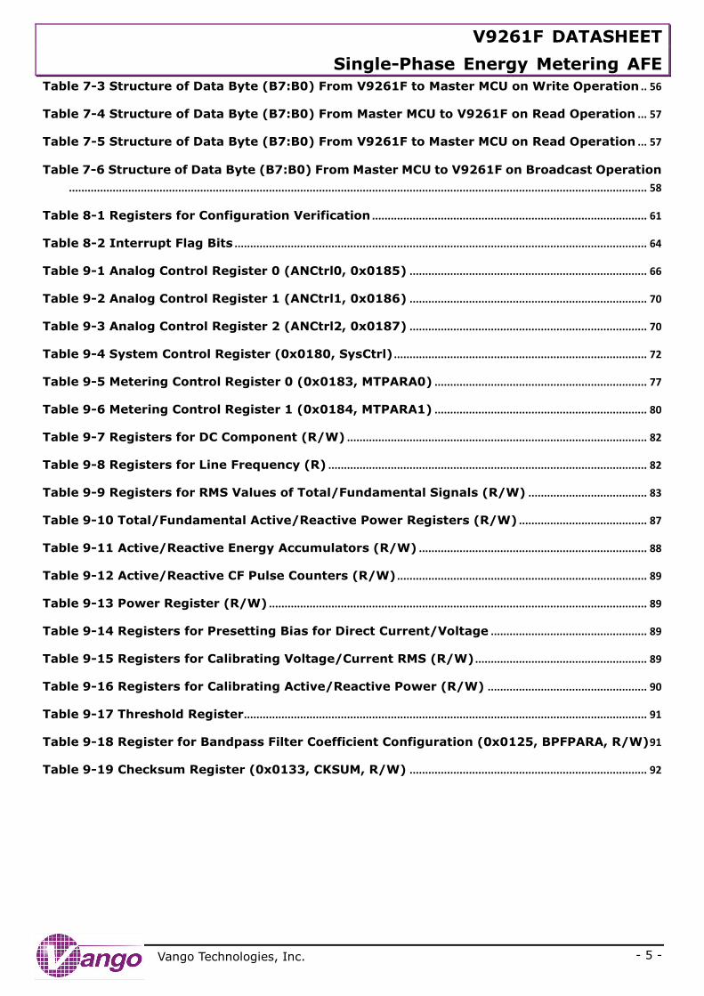
1. Reset
In V9261F, the chip will be reset to the Default State when a POR, RX reset, or global software reset
occurs.
1.1. Power-On Reset (POR)
In V9261F, the internal power-on reset circuit supervises the output voltage on pin “DVCC” all the
time. When the output voltage is lower than 1.45 V, the reset signal will be generated and force the chip
into the reset state. When the output voltage is higher than 1.45 V, the reset signal will be released and
the chip will get to the Default State in 500 μs.
When a POR event occurs, the bit “RSTSRC” (bit[26:24] of SysCtrl, 0x0180) will be reset to
“0b001”.
In the reset state, the master MCU and the Vango metering architecture cannot access RAM. When the
chip exits from the reset state, RAM will implement the self-checking in about 1.25 ms. If there is no error
occurring, RAM can be accessed.
In the reset state, the UART serial interface is idle. The UART serial interface starts to run immediately
once the chip exits from the reset state.
Internal reset
signal
RAM access
UART
communication
Reset state
VSS
1.45V
//
DVCC
500μs
When output voltage on pin DVCC is higher than 1.45V, the reset signal is released and the chip will exits from the reset state in 500μs.
RAMself-check1.25ms
1.75ms
When output voltage on pin DVCC is higher than 1.45V, the RAM can be accessed in about 1.75ms.
Figure 1-1 Timing of POR
V9261F DATASHEET
Single-Phase Energy Metering AFE
- 7 -
Vango Technologies, Inc.
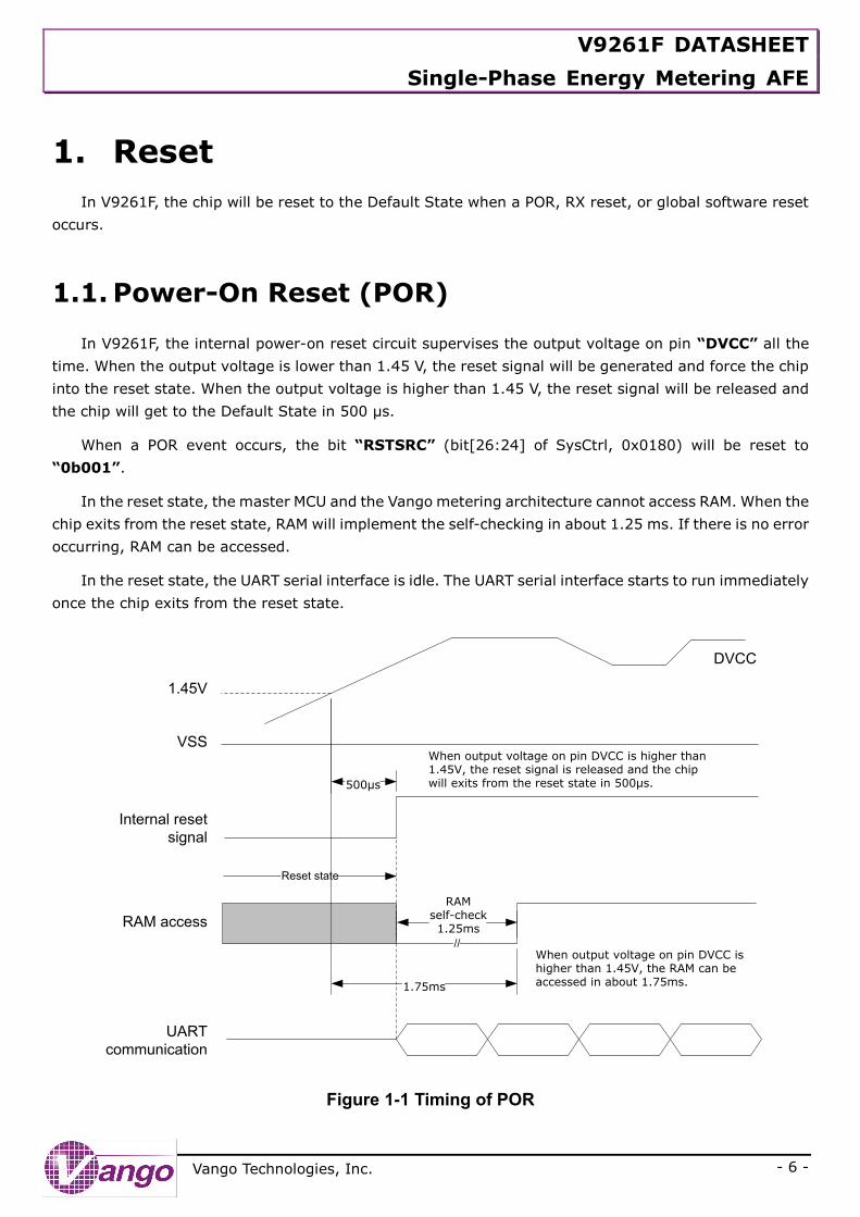
1.2. RX Reset
The input on pin “RX” must be driven low for at least 64 ms to force the chip into the reset state. Pull
to the logic high, and 900 μs later the chip will exit from the reset state and get back to the Default State.
When the “RX” reset occurs, the bit “RSTSRC” (bit[26:24] of SysCtrl, 0x0180) will be reset to
“0b011”.
In the reset state, the master MCU and the Vango metering architecture cannot access RAM. When the
chip exits from the reset state, RAM will implement the self-checking in about 1.25 ms. If there is no error
occurring, RAM can be accessed.
In the reset state, the UART serial interface is idle. The UART serial interface starts to run immediately
once the chip exits from the reset state.
//
Input on
“RX” pin
Internal reset
signal
64 ms
//
RAM access
UART
communication
Reset state
500 μs
900 μs
RAMself-checking
1.25 ms
The input on pin “RX” must be driven low for 64 ms to force the chip into the Reset State.
When the input on pin “RX” is pulled high, the chip will exit from the reset state in 900 µs and get back to the Default State.
2.15 ms
When the input on pin “RX” is pulled high, RAM can be accessed in 2.15 ms.
Figure 1-2 Timing of RX Reset
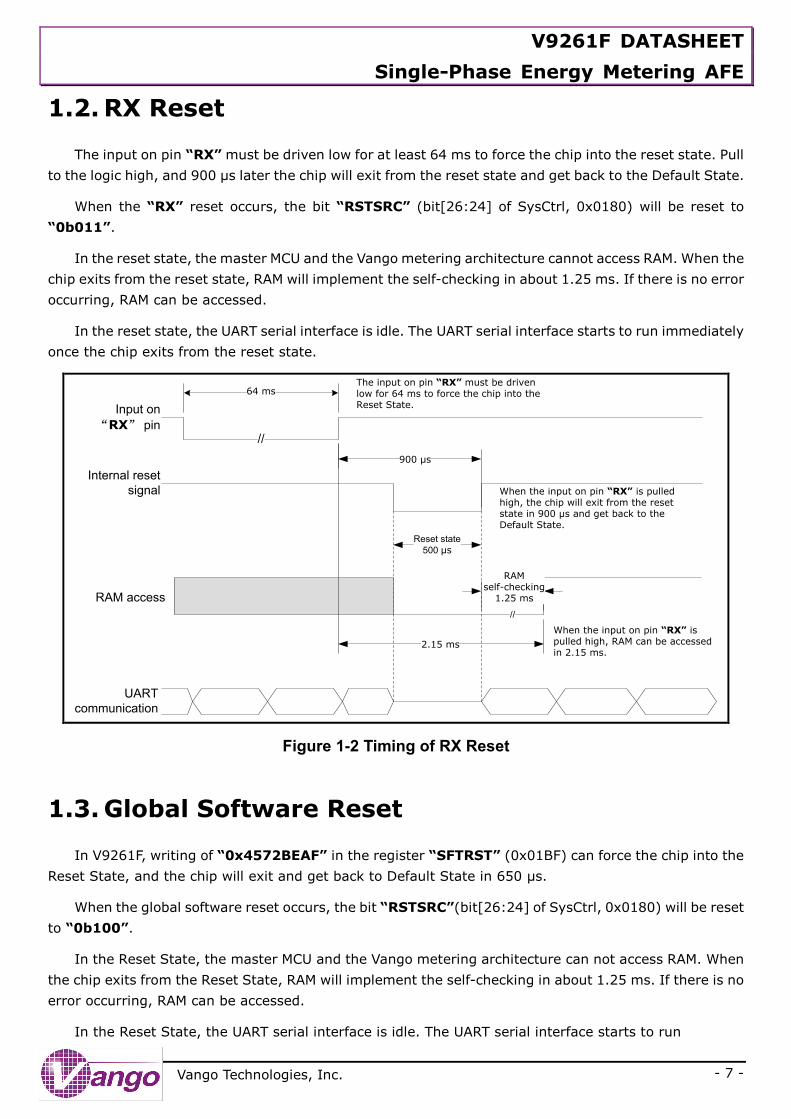
1.3. Global Software Reset
In V9261F, writing of “0x4572BEAF” in the register “SFTRST” (0x01BF) can force the chip into the
Reset State, and the chip will exit and get back to Default State in 650 μs.
When the global software reset occurs, the bit “RSTSRC”(bit[26:24] of SysCtrl, 0x0180) will be reset
to “0b100”.
In the Reset State, the master MCU and the Vango metering architecture can not access RAM. When
the chip exits from the Reset State, RAM will implement the self-checking in about 1.25 ms. If there is no
error occurring, RAM can be accessed.
In the Reset State, the UART serial interface is idle. The UART serial interface starts to run
V9261F DATASHEET
Single-Phase Energy Metering AFE
- 8 -
Vango Technologies, Inc.
immediately once the chip exits from the Reset State.
Internal reset
signal
RAM access
Writing of
register
“0x01BF”
//
Reset state
500 μs
0x4572BEAF
UART
communication
650 μs
Write of “0x4572BEAF” to register “0x01BF” to force the chip into the Reset State, and the chip will exit from the Reset State in 650 μs.
RAMself-checking
1.25 ms
1.9 msWrite of “0x4572BEAF” to register “0x01BF”, and 1.9 ms
later RAM can be accessed.
Figure 1-3 Timing of Global Software Reset
1.4. Registers
Table 1-1 Reset Related Registers
Register Bit Description
0x0180
SysCtrl
Bit[26:24]
RSTSRC
Flag bits to indicate the reset source
Bit26 Bit25 Bit24 Description
0 0 1 A POR event occurred.
0 0 0 Reserved.
0 1 1 An RX reset event occurred.
0 1 0 Reserved.
1 0 0 A global software reset occurred.
0x01BF, SFTRST
Software Reset Control
Register
Readable and writable, in the form of 32-bit 2’ complement.
Write “0x4572BEAF” to the register to reset the system.
V9261F DATASHEET
Single-Phase Energy Metering AFE
- 9 -
Vango Technologies, Inc.
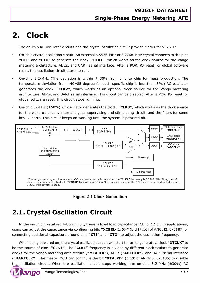
2. Clock
The on-chip RC oscillator circuits and the crystal oscillation circuit provide clocks for V9261F:
On-chip crystal oscillation circuit: An external 6.5536-MHz or 3.2768-MHz crystal connects to the pins
“CTI” and “CTO” to generate the clock, “CLK1”, which works as the clock source for the Vango
metering architecture, ADCs, and UART serial interface. After a POR, RX reset, or global software
reset, this oscillation circuit starts to run.
On-chip 3.2-MHz (The deviation is within ± 30% from chip to chip for mass production. The
temperature deviation from -40~85 degree for each specific chip is less then 3%.) RC oscillator
generates the clock, “CLK2”, which works as an optional clock source for the Vango metering
architecture, ADCs, and UART serial interface. This circuit can be disabled. After a POR, RX reset, or
global software reset, this circuit stops running.
On-chip 32-kHz (±50%) RC oscillator generates the clock, “CLK3”, which works as the clock source
for the wake-up circuit, internal crystal supervising and stimulating circuit, and the filters for some
key IO ports. This circuit keeps on working until the system is powered off.
6.5536 MHz/3.2768 MHz
6.5536 MHz/3.2768 MHz
XT½ DIV*
“CLK1”3.2768 MHz
“CLK2”3.2-MHz (±30%) RC
“CLK3”32-kHz(±50%) RC
Supervising and stimulating
circuit
ON
OFF
Metering clock
“MEACLK”
UART clock
“UARTCLK”
ADC clock
“ADCCLK”
Wake-up
IO ports filter
UDIV
ADIV
MDIV
*The Vango metering architecture and ADCs can work normally only when the “CLK1” frequency is 3.2768 MHz. Thus, the 1/2 divider must be enabled to divide “XTCLK” by 2 when a 6.5536-MHz crystal is used, or the 1/2 divider must be disabled when a 3.2768-MHz crystal is used.
Figure 2-1 Clock Generation
2.1. Crystal Oscillation Circuit
In the on-chip crystal oscillation circuit, there is fixed load capacitance (CL) of 12 pF. In applications,
users can adjust the capacitance via configuring bits “XCSEL<1:0>” (bit[17:16] of ANCtrl2, 0x0187) or
connecting additional capacitors around pins “CTI” and “CTO” to adjust the oscillation frequency.
When being powered on, the crystal oscillation circuit will start to run to generate a clock “XTCLK” to
be the source of clock “CLK1”. The “CLK1” frequency is divided by different clock scalars to generate
clocks for the Vango metering architecture (“MEACLK”), ADCs (“ADCCLK”), and UART serial interface
(“UARTCLK”). The master MCU can configure the bit “XTALPD” (bit20 of ANCtrl0, 0x0185) to disable
the oscillation circuit. When the oscillation circuit stops working, the on-chip 3.2-MHz (±30%) RC
V9261F DATASHEET
Single-Phase Energy Metering AFE
- 10 -
Vango Technologies, Inc.
oscillator will start to run automatically to generate clock “CLK2” to replace “CLK1” to provide clock
pulses for the metering architecture, ADCs, and UART serial interface. However, please note that the
“CLK2” frequency is not accurate enough for the UART communication.
Both 3.2768-MHz and 6.5536-MHz crystals can be connected around the pins “CTI” and “CTO”. Thus,
the “XTCLK” frequency can be 3.2768 MHz or 6.5536 MHz. But the Vango metering architecture and
ADCs can work normally only when the CLK1 frequency is 3.2768 MHz. So, the 1/2 divider must be
enabled when a 6.5536-MHz crystal is used; otherwise, it must be disabled. Users can enable or disable
this divider via configuring the bit “XTAL3P2M” (bit19 of ANCtlr0, 0x0185).
Please note the 1/2 divider is enabled after a POR, RX reset, or global software reset occurs. So the UART
interface will communicate at a half of the expected baud rate when 3.2768-MHz crystal is used. Users
must disable the 1/2 divider via the bit “XTAL3P2M” (bit19 of ANCtrl0, 0x0185).
Users can adjust the clock frequency for ADCs and metering architecture via bits
“ADCCLKSEL<1:0>” (bit[17:16] of ANCtrl0, 0x0185) and “CKMDIV” (bit1 of SysCtrl, 0x0180).
The typical power dissipation of the crystal oscillation circuit is 130 μA. When a 3.2768-MHz crystal is
used, users must set bit “XTALLP” to ‘1’ to lower the power dissipation to a half. When a 6.5536-MHz
crystal is used, setting this bit has no effect on the power dissipation of this circuit. When a crystal of
higher than 60-Ω ESR (Equivalent Serial Resistance) is used, users must set the bit “XRSEL<0>” (bit18
of ANCtrl2, 0x0187) to ‘1’ to improve the driving ability of the oscillation circuit to ensure the crystal to
work, which needs additional 55-μA load current.
In the Metering Mode, some errors can stop the oscillation circuit. So, an internal supervising and
stimulating circuit, which is sourced by “CLK3”, is designed to monitor the crystal all the time. When the
crystal stops oscillating, this circuit will generate a 1-ms wide pulse every second to stimulate the crystal
to restore oscillating. The stimulating function of this circuit is disabled by default. Users can set the bit
“XRSTEN” (bit21 of ANCtrl0, 0x0185) to ‘1’ to enable this function.
In the Sleep Mode, this crystal oscillation circuit stops working, and it will not get back to work
automatically even though the system is woken up from the Sleep Mode to get to the Current Detection
Mode.
When the crystal stops working, an interrupt signal will be generated and the flag bit “HSEFAIL”
(bit27 of SysCtrl, 0x0180) is set to ‘1’, which will be cleared when the crystal restores to work.
Please note that the “CLK2” frequency is not accurate enough for the UART communication, so the
master MCU cannot read the actual state of the flag bit “HSEFAIL”.
2.2. 3.2-MHz RC Oscillator
In V9261F, an on-chip 3.2-MHz RC oscillator is designed to generate a 3.2768-MHz (The deviation is
within ±30% from chip to chip for mass production. The temperature deviation from -40~85 degree for
each specific chip is less than 3%.) clock, “CLK2”, to work as an optional clock source for the Vango
metering architecture, ADCs, and UART serial interface. But the “CLK2” frequency is not accurate enough
for the UART communication. In the Metering Mode, this circuit will start to run automatically when the
crystal stops working, and it will stop running automatically when the crystal restores to work.

V9261F DATASHEET
Single-Phase Energy Metering AFE
- 11 -
Vango Technologies, Inc.
After a POR, RX reset, or global software reset occurs, this circuit stops running. To enable this circuit,
it is mandatory to enable the BandGap and global biasing current circuits firstly which provide the biasing
current and reference voltage for the 3.2-MHz RC oscillator.
In the Sleep Mode, this circuit stops running, and it will get back to work automatically when the chip
is woken up from the Sleep Mode to get to the Current Detection Mode.
2.3. 32-kHz RC Oscillator
The on-chip 32-kHz RC oscillator can generate a 32-kHz (±50%) RC clock, “CLK3”, to drive the
wake-up circuit, internal crystal supervising and stimulating circuit, and the filters for some key IO ports.
This oscillator cannot be disabled until the system is powered off.
V9261F DATASHEET
Single-Phase Energy Metering AFE
- 12 -
Vango Technologies, Inc.
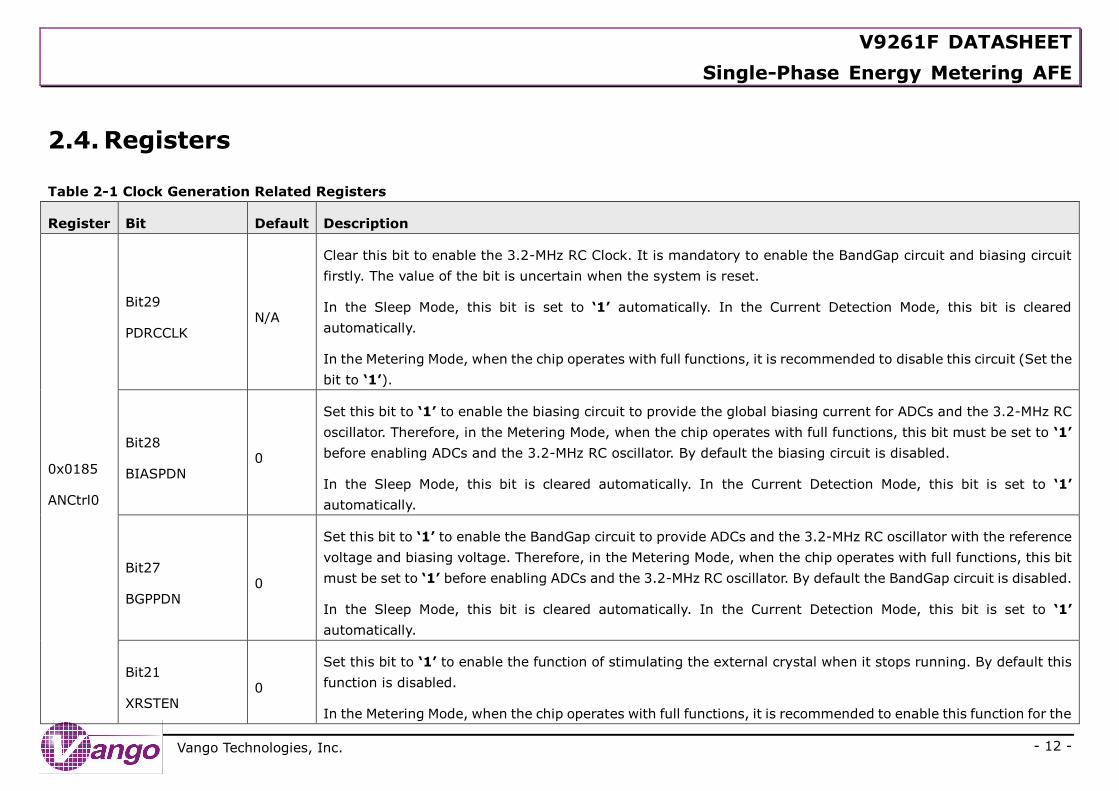
2.4. Registers
Table 2-1 Clock Generation Related Registers
Register Bit Default Description
0x0185
ANCtrl0
Bit29
PDRCCLK N/A
Clear this bit to enable the 3.2-MHz RC Clock. It is mandatory to enable the BandGap circuit and biasing circuit
firstly. The value of the bit is uncertain when the system is reset.
In the Sleep Mode, this bit is set to ‘1’ automatically. In the Current Detection Mode, this bit is cleared
automatically.
In the Metering Mode, when the chip operates with full functions, it is recommended to disable this circuit (Set the
bit to ‘1’).
Bit28
BIASPDN 0
Set this bit to ‘1’ to enable the biasing circuit to provide the global biasing current for ADCs and the 3.2-MHz RC
oscillator. Therefore, in the Metering Mode, when the chip operates with full functions, this bit must be set to ‘1’
before enabling ADCs and the 3.2-MHz RC oscillator. By default the biasing circuit is disabled.
In the Sleep Mode, this bit is cleared automatically. In the Current Detection Mode, this bit is set to ‘1’
automatically.
Bit27
BGPPDN 0
Set this bit to ‘1’ to enable the BandGap circuit to provide ADCs and the 3.2-MHz RC oscillator with the reference
voltage and biasing voltage. Therefore, in the Metering Mode, when the chip operates with full functions, this bit
must be set to ‘1’ before enabling ADCs and the 3.2-MHz RC oscillator. By default the BandGap circuit is disabled.
In the Sleep Mode, this bit is cleared automatically. In the Current Detection Mode, this bit is set to ‘1’
automatically.
Bit21
XRSTEN 0
Set this bit to ‘1’ to enable the function of stimulating the external crystal when it stops running. By default this
function is disabled.
In the Metering Mode, when the chip operates with full functions, it is recommended to enable this function for the
V9261F DATASHEET
Single-Phase Energy Metering AFE
- 13 -
Vango Technologies, Inc.
Register Bit Default Description
best performance.
Bit20
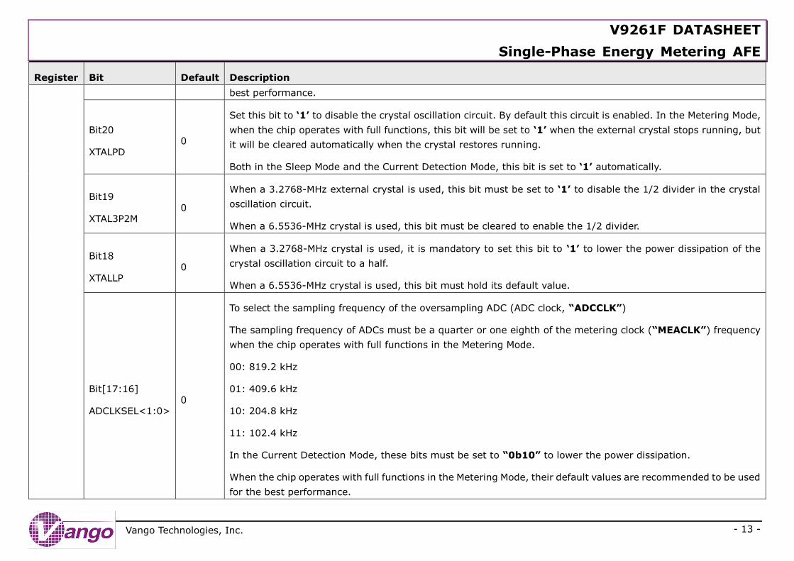
XTALPD 0
Set this bit to ‘1’ to disable the crystal oscillation circuit. By default this circuit is enabled. In the Metering Mode,
when the chip operates with full functions, this bit will be set to ‘1’ when the external crystal stops running, but
it will be cleared automatically when the crystal restores running.
Both in the Sleep Mode and the Current Detection Mode, this bit is set to ‘1’ automatically.
Bit19
XTAL3P2M 0
When a 3.2768-MHz external crystal is used, this bit must be set to ‘1’ to disable the 1/2 divider in the crystal
oscillation circuit.
When a 6.5536-MHz crystal is used, this bit must be cleared to enable the 1/2 divider.
Bit18
XTALLP 0
When a 3.2768-MHz crystal is used, it is mandatory to set this bit to ‘1’ to lower the power dissipation of the
crystal oscillation circuit to a half.
When a 6.5536-MHz crystal is used, this bit must hold its default value.
Bit[17:16]
ADCLKSEL<1:0> 0
To select the sampling frequency of the oversampling ADC (ADC clock, “ADCCLK”)
The sampling frequency of ADCs must be a quarter or one eighth of the metering clock (“MEACLK”) frequency
when the chip operates with full functions in the Metering Mode.
00: 819.2 kHz
01: 409.6 kHz
10: 204.8 kHz
11: 102.4 kHz
In the Current Detection Mode, these bits must be set to “0b10” to lower the power dissipation.
When the chip operates with full functions in the Metering Mode, their default values are recommended to be used
for the best performance.
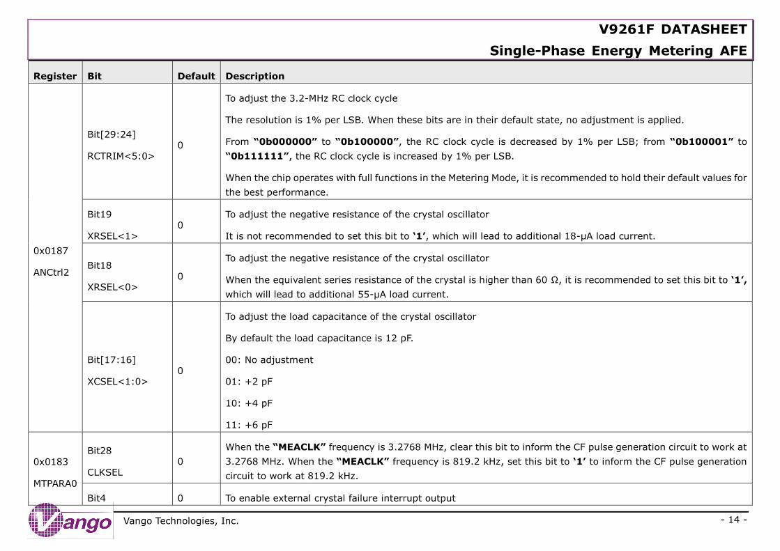
V9261F DATASHEET
Single-Phase Energy Metering AFE
- 14 -
Vango Technologies, Inc.
Register Bit Default Description
0x0187
ANCtrl2
Bit[29:24]
RCTRIM<5:0> 0
To adjust the 3.2-MHz RC clock cycle
The resolution is 1% per LSB. When these bits are in their default state, no adjustment is applied.
From “0b000000” to “0b100000”, the RC clock cycle is decreased by 1% per LSB; from “0b100001” to
“0b111111”, the RC clock cycle is increased by 1% per LSB.
When the chip operates with full functions in the Metering Mode, it is recommended to hold their default values for
the best performance.
Bit19
XRSEL<1> 0
To adjust the negative resistance of the crystal oscillator
It is not recommended to set this bit to ‘1’, which will lead to additional 18-μA load current.
Bit18
XRSEL<0> 0
To adjust the negative resistance of the crystal oscillator
When the equivalent series resistance of the crystal is higher than 60 Ω, it is recommended to set this bit to ‘1’,
which will lead to additional 55-μA load current.
Bit[17:16]
XCSEL<1:0> 0
To adjust the load capacitance of the crystal oscillator
By default the load capacitance is 12 pF.
00: No adjustment
01: +2 pF
10: +4 pF
11: +6 pF
0x0183
MTPARA0
Bit28
CLKSEL 0
When the “MEACLK” frequency is 3.2768 MHz, clear this bit to inform the CF pulse generation circuit to work at
3.2768 MHz. When the “MEACLK” frequency is 819.2 kHz, set this bit to ‘1’ to inform the CF pulse generation
circuit to work at 819.2 kHz.
Bit4 0 To enable external crystal failure interrupt output
V9261F DATASHEET
Single-Phase Energy Metering AFE
- 15 -
Vango Technologies, Inc.
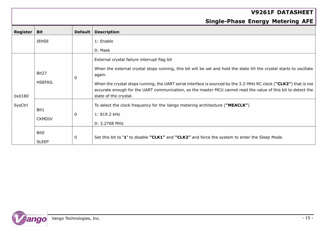
Register Bit Default Description
IEHSE 1: Enable
0: Mask
0x0180
SysCtrl
Bit27
HSEFAIL 0
External crystal failure interrupt flag bit
When the external crystal stops running, this bit will be set and hold the state till the crystal starts to oscillate
again.
When the crystal stops running, the UART serial interface is sourced by the 3.2-MHz RC clock (“CLK2”) that is not
accurate enough for the UART communication, so the master MCU cannot read the value of this bit to detect the
state of the crystal.
Bit1
CKMDIV 0
To select the clock frequency for the Vango metering architecture (“MEACLK”)
1: 819.2 kHz
0: 3.2768 MHz
Bit0
SLEEP 0 Set this bit to ‘1’ to disable “CLK1” and “CLK2” and force the system to enter the Sleep Mode.
V9261F DATASHEET
Single-Phase Energy Metering AFE
- 16 -
Vango Technologies, Inc.
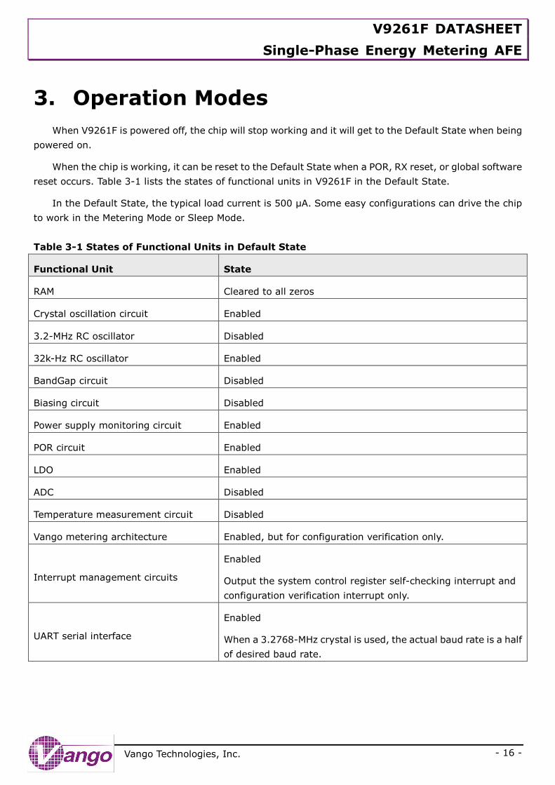
3. Operation Modes
When V9261F is powered off, the chip will stop working and it will get to the Default State when being
powered on.
When the chip is working, it can be reset to the Default State when a POR, RX reset, or global software
reset occurs. Table 3-1 lists the states of functional units in V9261F in the Default State.
In the Default State, the typical load current is 500 μA. Some easy configurations can drive the chip
to work in the Metering Mode or Sleep Mode.
Table 3-1 States of Functional Units in Default State
Functional Unit State
RAM Cleared to all zeros
Crystal oscillation circuit Enabled
3.2-MHz RC oscillator Disabled
32k-Hz RC oscillator Enabled
BandGap circuit Disabled
Biasing circuit Disabled
Power supply monitoring circuit Enabled
POR circuit Enabled
LDO Enabled
ADC Disabled
Temperature measurement circuit Disabled
Vango metering architecture Enabled, but for configuration verification only.
Interrupt management circuits
Enabled
Output the system control register self-checking interrupt and
configuration verification interrupt only.
UART serial interface
Enabled
When a 3.2768-MHz crystal is used, the actual baud rate is a half
of desired baud rate.
V9261F DATASHEET
Single-Phase Energy Metering AFE
- 17 -
Vango Technologies, Inc.
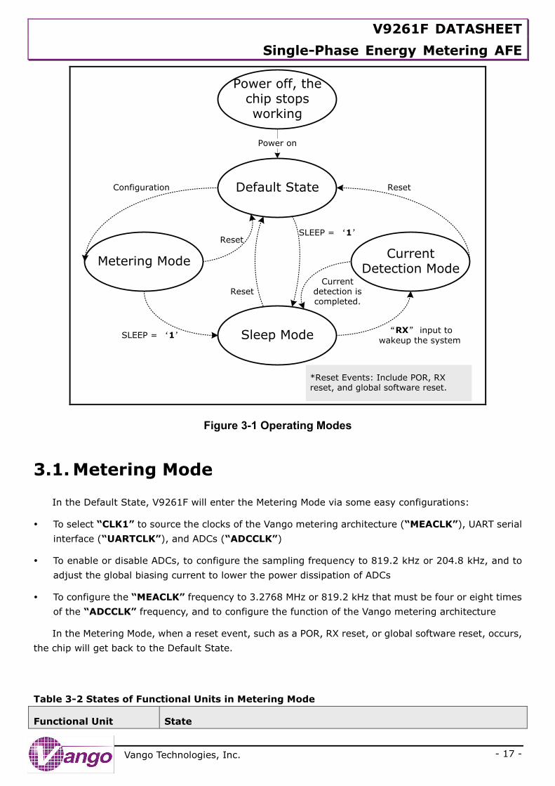
*Reset Events: Include POR, RX reset, and global software reset.
Power off, the chip stops working
Default State
Sleep Mode
Metering ModeCurrent
Detection Mode
Power on
Configuration
SLEEP = ‘1’
SLEEP = ‘1’Reset
Reset
“RX” input to
wakeup the system
Current detection is completed.
Reset
Figure 3-1 Operating Modes
3.1. Metering Mode
In the Default State, V9261F will enter the Metering Mode via some easy configurations:
To select “CLK1” to source the clocks of the Vango metering architecture (“MEACLK”), UART serial
interface (“UARTCLK”), and ADCs (“ADCCLK”)
To enable or disable ADCs, to configure the sampling frequency to 819.2 kHz or 204.8 kHz, and to
adjust the global biasing current to lower the power dissipation of ADCs
To configure the “MEACLK” frequency to 3.2768 MHz or 819.2 kHz that must be four or eight times
of the “ADCCLK” frequency, and to configure the function of the Vango metering architecture
In the Metering Mode, when a reset event, such as a POR, RX reset, or global software reset, occurs,
the chip will get back to the Default State.
Table 3-2 States of Functional Units in Metering Mode
Functional Unit State
V9261F DATASHEET
Single-Phase Energy Metering AFE
- 18 -
Vango Technologies, Inc.
Functional Unit State
Crystal oscillation circuit Enabled by default. It is mandatory to set bit “XRSTEN” to ‘1’ to enable the
function of stimulating the external crystal when it stops running.
3.2-MHz RC oscillator
It is recommended to disable this unit to lower the power dissipation. When
the crystal oscillation circuit stops running, this unit will start to run
automatically.
32-kHz RC oscillator Enabled
BandGap circuit It is mandatory to enable this unit.
Biasing circuit It is mandatory to enable this unit.
Power supply monitoring
circuit Enabled
POR circuit Enabled
LDO
Enabled
Configure the DVCCLDO to lower power dissipation of the Vango metering
architecture.
ADC Enable ADCs, configure the sampling frequency, and adjust the global biasing
current to lower the power dissipation, to meet the application requirements.
Temperature
measurement circuit Enable or disable to meet the application requirements.
Vango metering
architecture
It is mandatory to enable this unit, and configure its functions to meet the
application requirements.
Interrupt management
circuits
Enabled
Output system control register self-checking interrupt and configuration
verification interrupt all the time, and output the desired interrupts to meet
the application requirements.
UART serial interface Enabled
3.2. Sleep Mode
When V9261F is in the Default State or Metering Mode, set the bit “SLEEP” (bit0, SysCtrl, 0x0180) to
‘1’ to enable the system to enter the Sleep Mode.
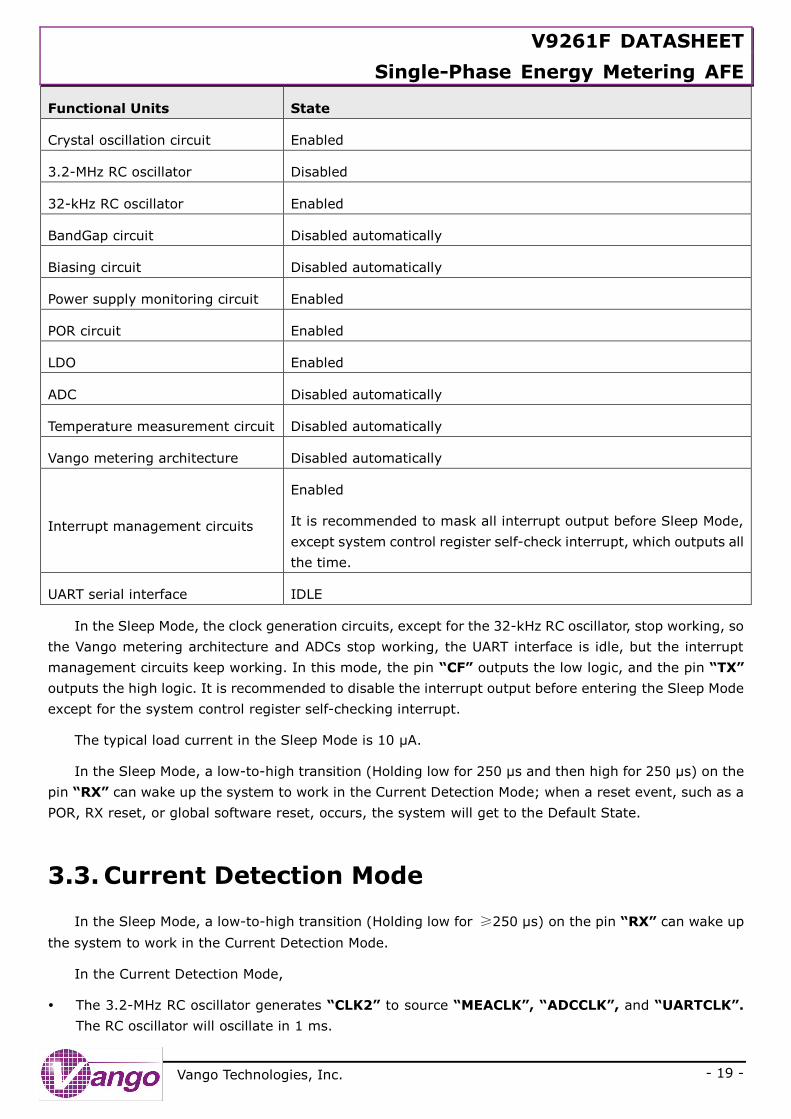
Table 3-3 States of Functional Units in Sleep Mode
Functional Units State
V9261F DATASHEET
Single-Phase Energy Metering AFE
- 19 -
Vango Technologies, Inc.
Functional Units State
Crystal oscillation circuit Enabled
3.2-MHz RC oscillator Disabled
32-kHz RC oscillator Enabled
BandGap circuit Disabled automatically
Biasing circuit Disabled automatically
Power supply monitoring circuit Enabled
POR circuit Enabled
LDO Enabled
ADC Disabled automatically
Temperature measurement circuit Disabled automatically
Vango metering architecture Disabled automatically
Interrupt management circuits
Enabled
It is recommended to mask all interrupt output before Sleep Mode,
except system control register self-check interrupt, which outputs all
the time.
UART serial interface IDLE
In the Sleep Mode, the clock generation circuits, except for the 32-kHz RC oscillator, stop working, so
the Vango metering architecture and ADCs stop working, the UART interface is idle, but the interrupt
management circuits keep working. In this mode, the pin “CF” outputs the low logic, and the pin “TX”
outputs the high logic. It is recommended to disable the interrupt output before entering the Sleep Mode
except for the system control register self-checking interrupt.
The typical load current in the Sleep Mode is 10 μA.
In the Sleep Mode, a low-to-high transition (Holding low for 250 μs and then high for 250 μs) on the
pin “RX” can wake up the system to work in the Current Detection Mode; when a reset event, such as a
POR, RX reset, or global software reset, occurs, the system will get to the Default State.
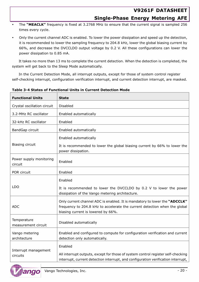
3.3. Current Detection Mode
In the Sleep Mode, a low-to-high transition (Holding low for ≥250 μs) on the pin “RX” can wake up
the system to work in the Current Detection Mode.
In the Current Detection Mode,
The 3.2-MHz RC oscillator generates “CLK2” to source “MEACLK”, “ADCCLK”, and “UARTCLK”.
The RC oscillator will oscillate in 1 ms.
V9261F DATASHEET
Single-Phase Energy Metering AFE
- 20 -
Vango Technologies, Inc.
The “MEACLK” frequency is fixed at 3.2768 MHz to ensure that the current signal is sampled 256
times every cycle.
Only the current channel ADC is enabled. To lower the power dissipation and speed up the detection,
it is recommended to lower the sampling frequency to 204.8 kHz, lower the global biasing current by
66%, and decrease the DVCCLDO output voltage by 0.2 V. All these configurations can lower the
power dissipation to 0.85 mA.
It takes no more than 13 ms to complete the current detection. When the detection is completed, the
system will get back to the Sleep Mode automatically.
In the Current Detection Mode, all interrupt outputs, except for those of system control register
self-checking interrupt, configuration verification interrupt, and current detection interrupt, are masked.
Table 3-4 States of Functional Units in Current Detection Mode
Functional Units State
Crystal oscillation circuit Disabled
3.2-MHz RC oscillator Enabled automatically
32-kHz RC oscillator Enabled
BandGap circuit Enabled automatically
Biasing circuit
Enabled automatically
It is recommended to lower the global biasing current by 66% to lower the
power dissipation.
Power supply monitoring
circuit Enabled
POR circuit Enabled
LDO
Enabled
It is recommended to lower the DVCCLDO by 0.2 V to lower the power
dissipation of the Vango metering architecture.
ADC
Only current channel ADC is enabled. It is mandatory to lower the “ADCCLK”
frequency to 204.8 kHz to accelerate the current detection when the global
biasing current is lowered by 66%.
Temperature
measurement circuit Disabled automatically
Vango metering
architecture
Enabled and configured to compute for configuration verification and current
detection only automatically.
Interrupt management
circuits
Enabled
All interrupt outputs, except for those of system control register self-checking
interrupt, current detection interrupt, and configuration verification interrupt,
V9261F DATASHEET
Single-Phase Energy Metering AFE
- 21 -
Vango Technologies, Inc.
are masked.
UART serial interface The “UARTCLK” frequency is not accurate enough for the UART
communication.
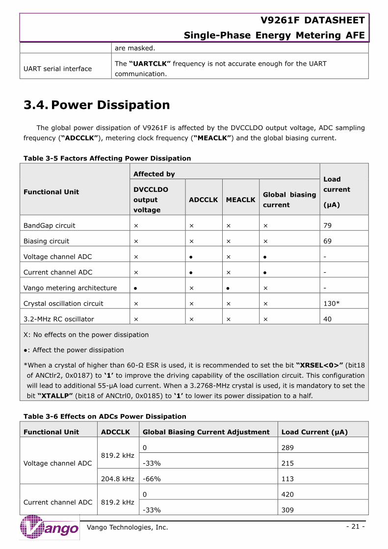
3.4. Power Dissipation
The global power dissipation of V9261F is affected by the DVCCLDO output voltage, ADC sampling
frequency (“ADCCLK”), metering clock frequency (“MEACLK”) and the global biasing current.
Table 3-5 Factors Affecting Power Dissipation
Functional Unit
Affected by Load
current
(μA)
DVCCLDO
output
voltage
ADCCLK MEACLK Global biasing
current
BandGap circuit × × × × 79
Biasing circuit × × × × 69
Voltage channel ADC × ● × ● -
Current channel ADC × ● × ● -
Vango metering architecture ● × ● × -
Crystal oscillation circuit × × × × 130*
3.2-MHz RC oscillator × × × × 40
X: No effects on the power dissipation
●: Affect the power dissipation
*When a crystal of higher than 60-Ω ESR is used, it is recommended to set the bit “XRSEL<0>” (bit18
of ANCtlr2, 0x0187) to ‘1’ to improve the driving capability of the oscillation circuit. This configuration
will lead to additional 55-μA load current. When a 3.2768-MHz crystal is used, it is mandatory to set the
bit “XTALLP” (bit18 of ANCtrl0, 0x0185) to ‘1’ to lower its power dissipation to a half.
Table 3-6 Effects on ADCs Power Dissipation
Functional Unit ADCCLK Global Biasing Current Adjustment Load Current (μA)
Voltage channel ADC 819.2 kHz
0 289
-33% 215
204.8 kHz -66% 113
Current channel ADC 819.2 kHz 0 420
-33% 309
V9261F DATASHEET
Single-Phase Energy Metering AFE
- 22 -
Vango Technologies, Inc.
Functional Unit ADCCLK Global Biasing Current Adjustment Load Current (μA)
204.8 kHz -66% 155
Table 3-7 Effect on Vango metering architecture Power Dissipation
Functional Unit MEACLK DVCCLDO Output Voltage
Adjustment Load Current (μA)
Vango metering
architecture 3.2768 MHz
0 720
+0.2V 782
The “MEACLK” frequency can affect the power dissipation of the Vango metering architecture. But lower
the “MEACLK” frequency weakens the metering accuracy, and slows down the voltage and current RMS
update. So in the Metering Mode, users should not adjust the “MEACLK” frequency to lower the power
dissipation.
The configuration of bits “MEAS” (bit[7:5] of SysCtrl, 0x0180) has effects on the power dissipation of
the various signal measurement channel.
Table 3-8 Power Dissipation of Measurement Channel
Test Condition Configuration of “MEAS”
Bit[7:5] of SysCtrl, 0x0180 Load Current (μA)
DVCCLDO output voltage
adjustment: +0 V
“ADCCLK” frequency: 819.2 kHz
“MEACLK” frequency:
3.2768 MHz
Global biasing current
adjustment: -33%
000: Current input on pins “IBP”/“IBN” 523
100: Temperature 699
101: Ground 819
110: Ground 819
111: Ground 889
V9261F DATASHEET
Single-Phase Energy Metering AFE
- 23 -
Vango Technologies, Inc.
The following table lists the typical power dissipation in each operating mode.
Table 3-9 Power Dissipation in Each Operating Mode
Operating Mode
Metering Mode (Only voltage
and current channels are
enabled) Current
Detection
Mode
Sleep
Mode Configuration
1
Configuration
2
Test C
onditio
n
DVCCLDO Output Voltage
Adjustment 0 0 -0.2 V 0
ADCCLK Frequency 819.2 kHz 819.2 kHz 204.8 kHz -
MEACLK Frequency 3.2768 MHz 3.2768 MHz 3.2768 MHz -
Global Biasing Current
Adjustment -33% -33% -66% 0
Crystal Oscillation Circuit 6.5536 MHz 3.2768 MHz Disabled Disabled
3.2-MHz RC Oscillator Disabled Disabled Enabled Disabled
Typical Load Current 1.61 mA 1.55 mA 0.85 mA 10 μA
V9261F DATASHEET
Single-Phase Energy Metering AFE
- 24 -
Vango Technologies, Inc.
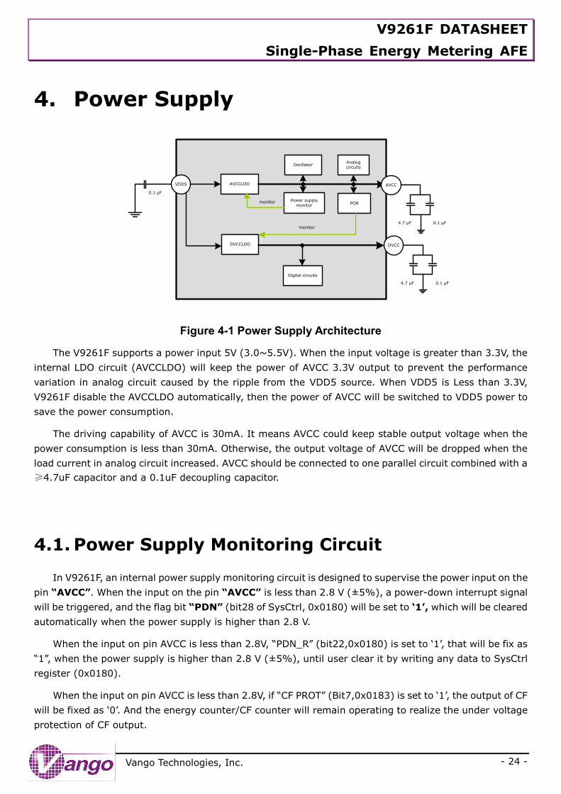
4. Power Supply
VDD5
Analog circuits
DVCCLDO
Digital circuits
Oscillator
DVCC
Power supply monitor
POR
4.7 μF 0.1 μF
0.1 μF
AVCCLDO
monitor
AVCC
4.7 μF 0.1 μF
monitor
Figure 4-1 Power Supply Architecture
The V9261F supports a power input 5V (3.0~5.5V). When the input voltage is greater than 3.3V, the
internal LDO circuit (AVCCLDO) will keep the power of AVCC 3.3V output to prevent the performance
variation in analog circuit caused by the ripple from the VDD5 source. When VDD5 is Less than 3.3V,
V9261F disable the AVCCLDO automatically, then the power of AVCC will be switched to VDD5 power to
save the power consumption.
The driving capability of AVCC is 30mA. It means AVCC could keep stable output voltage when the
power consumption is less than 30mA. Otherwise, the output voltage of AVCC will be dropped when the
load current in analog circuit increased. AVCC should be connected to one parallel circuit combined with a
≥4.7uF capacitor and a 0.1uF decoupling capacitor.
4.1. Power Supply Monitoring Circuit
In V9261F, an internal power supply monitoring circuit is designed to supervise the power input on the
pin “AVCC”. When the input on the pin “AVCC” is less than 2.8 V (±5%), a power-down interrupt signal
will be triggered, and the flag bit “PDN” (bit28 of SysCtrl, 0x0180) will be set to ‘1’, which will be cleared
automatically when the power supply is higher than 2.8 V.
When the input on pin AVCC is less than 2.8V, “PDN_R” (bit22,0x0180) is set to ‘1’, that will be fix as
“1”, when the power supply is higher than 2.8 V (±5%), until user clear it by writing any data to SysCtrl
register (0x0180).
When the input on pin AVCC is less than 2.8V, if “CF PROT” (Bit7,0x0183) is set to ‘1’, the output of CF
will be fixed as ‘0’. And the energy counter/CF counter will remain operating to realize the under voltage
protection of CF output.
V9261F DATASHEET
Single-Phase Energy Metering AFE
- 25 -
Vango Technologies, Inc.
AVCC
2.8V(±5%)
PDN flag
PDN_R flag
CF
CLR operation
Figure 4-2 Power-Down Interrupt
4.2. Digital Power Supply
The digital power supply(DVCCLDO) for digital circuits is derived by an on-chip LDO from the
AVCCLDO. This DVCCLDO keeps working even though the system is powered down.
This DVCCLDO has a driving capability of 35 mA, which means when the load current on the digital
circuits is less than 35 mA, this DVCCLDO will output the stable voltage; but when the load current is
higher than 35 mA, the output will reduce as the current increases.
It is recommended to decouple the pin “DVCC” externally with a ≥ 4.7-μF capacitor in parallel with
a 0.1-μF capacitor.
4.3. Registers
Table 4-1 DVCCLDO Output Voltage Adjustment
Register Bit Default Description
ANCtrl2
0x0187
Bit[14:12]
LDOVSEL<2:0> 0
To adjust the DVCCLDO output voltage
000: No adjustment
001: -0.1 V
010: +0.2 V
V9261F DATASHEET
Single-Phase Energy Metering AFE
- 26 -
Vango Technologies, Inc.
011: +0.1 V
100: -0.4 V
101: -0.5 V
110: -0.2 V
111: -0.3 V
V9261F DATASHEET
Single-Phase Energy Metering AFE
- 27 -
Vango Technologies, Inc.
5. BandGap Circuit
In V9261F, the BandGap circuit outputs a reference voltage and bias voltage, about 1.188 V with a
typical temperature coefficient of 10 ppm/˚C, for ADCs and the 3.2-MHz RC oscillator. The BandGap circuit
must be enabled before ADCs and the RC oscillator, and typically, this circuit consumes about 0.08 mA.
By default the BandGap circuit is disabled. Users can set the bit “BGPPDN” (bit27 of ANCtrl0, 0x0185)
to ‘1’ to enable the BandGap circuit. In the Sleep Mode, this circuit is disabled automatically; and in the
Current Detection Mode, this circuit is enabled automatically.
Users can configure “bit[14:12]” and “bit[9:8]” of “ANCtrl0” register (0x0185) to adjust the
temperature coefficient to reduce the temperature coefficient drift introduced by the external components,
with the following steps:
1) Assume the current settings of relative bits are REST<2:0>=’010’ and RESTL<1:0>=’00’, which
means an additional +20ppm for temperature coefficient of BandGap.
2) Measure meter errors in high and low temperature conditions. Assume user has calibrated the
meter error to 0 at 20℃, and the measuring errors are 0.6% at 80℃ and -0.4% at -40℃ separately. Then
a -(0.6%-(-0.4%))/2=-0.5% measuring error needs to be compensated relative to high temperature
working condition, equivalent to -0.5%/(80-20)=-5000/60=-83ppm, rounding to -80ppm.
3) As measuring error is minus two times of REF temperature coefficient error, to compensate a
-80ppm error, an additional +40ppm of BandGap REF temperature coefficient adjustment is needed.
Taking the initial +20ppm setting into consideration, the actual adjustment should be +60ppm. According
to the lookup table of RESTL<1:0> and REST<2:0>, user should set register RESTL<1:0> to ‘01’ and
REST<2:0> to ‘111’, whose combination equals to a +60ppm temperature coefficient adjustment.
A temperature coefficient drift of “x” in the BandGap circuit results in a drift of “-2x” in the measurement
error.
Table 5-1 Configuration for BandGap Circuit
Register bit Description
ANCtrl0,
0x0185,
R/W
Bit27
BGPPDN
Set this bit to ‘1’ to enable the BandGap circuit to provide ADCs and the
3.2-MHz RC oscillator with the reference voltage and biasing voltage.
Therefore, in the Metering Mode, this bit must be set to ‘1’ before enabling
ADCs and the 3.2-MHz RC oscillator. By default the BandGap circuit is
disabled.
In the Sleep Mode, this bit is cleared automatically. In the Current Detection
Mode, this bit is set to ‘1’ automatically.
Bit[14:12] To finely adjust the temperature coefficient of the BandGap circuit. In order
to obtain the best metering performance and temperature performance
V9261F DATASHEET
Single-Phase Energy Metering AFE
- 28 -
Vango Technologies, Inc.
Register bit Description
REST<2:0> during normal metering, it must be configured according to the calculated
result. The calculation method, please refer to BandGap Circuit chapter.
000: No adjustment
001: +10 ppm
010: +20 ppm
011: +30 ppm
100: -40 ppm
101: -30 ppm
110: -20 ppm
111: -10 ppm
Bit[9:8]
RESTL<1:0>
To roughly adjust the temperature coefficient of the BandGap circuit. In
order to obtain the best metering performance and temperature
performance during normal metering, it must be configured according to the
calculated result. The calculation method, please refer to BandGap Circuit
chapter.
00: 0
01: +70 ppm
10: -140 ppm
11: -70 ppm
V9261F DATASHEET
Single-Phase Energy Metering AFE
- 29 -
Vango Technologies, Inc.
6. Energy Metering
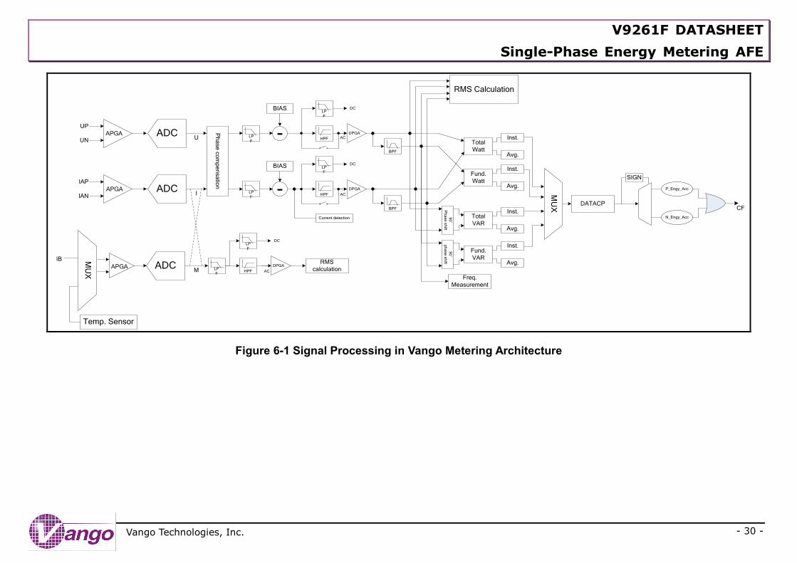
The Vango metering architecture in V9261F has features:
- 3 independent oversampling Σ/Δ ADCs: One for voltage (U), one for current (I) and one for various
signal measurement (M)
- High metering accuracy:
Less than 0.1% of active energy metering accuracy over dynamic range of 10000:1
Less than 0.1% of reactive energy metering accuracy over dynamic range of 5000:1
- Various measurements:
DC components of voltage/current signals
Total/Fundamental raw/instantaneous/average voltage/current RMS
Total/Fundamental raw/instantaneous/average active/reactive power
Positive/Negative energy, active/reactive selectable
Line frequency and temperature
- CF pulse output
- Current detection
- Supporting calibrating meters via software
- Accelerating meter calibration when low current is applied
V9261F DATASHEET
Single-Phase Energy Metering AFE
- 30 -
Vango Technologies, Inc.
APGA ADC
ADC
ADC
I
M
U
Ph
ase
co
mp
en
sa
tion
90˚
Ph
ase
sh
ift
90˚
ph
ase
sh
ift
APGA
APGA
UP
UN
IAP
IAN
CF
RMS Calculation
Total
Watt
Fund.
Watt
Total
VAR
Fund.
VAR
Inst.
Avg.
Inst.
Avg.
Inst.
Avg.
Inst.
Avg.
SIGN
P_Engy_Acc
N_Engy_Acc
MU
X
IB
DATACP
Freq.
Measurement
LP
FHPF
LP
F
DPGA
LP
FHPF
LP
F
DPGA
Current detection
BPF
BPF
LP
FHPF
LP
F
DPGARMS
calculation
DC
AC
DC
AC
AC
DCM
UX
-
-
BIAS
BIAS
Temp. Sensor
Figure 6-1 Signal Processing in Vango Metering Architecture
V9261F DATASHEET
Single-Phase Energy Metering AFE
- 31 -
Vango Technologies, Inc.
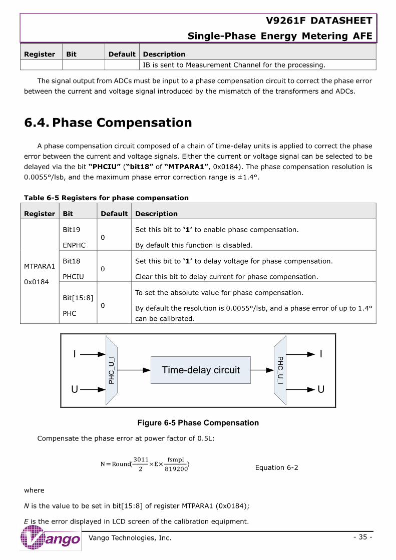
6.1. Metering Clock (“MEACLK”)
The metering clock (“MEACLK”) is sourced by “CLK1”, generated by crystal oscillation circuit, or
“CLK2”, generated by the 3.2-MHz RC oscillator. When both circuits stop running, the Vango metering
architecture will stop working.
6.2. Analog Input
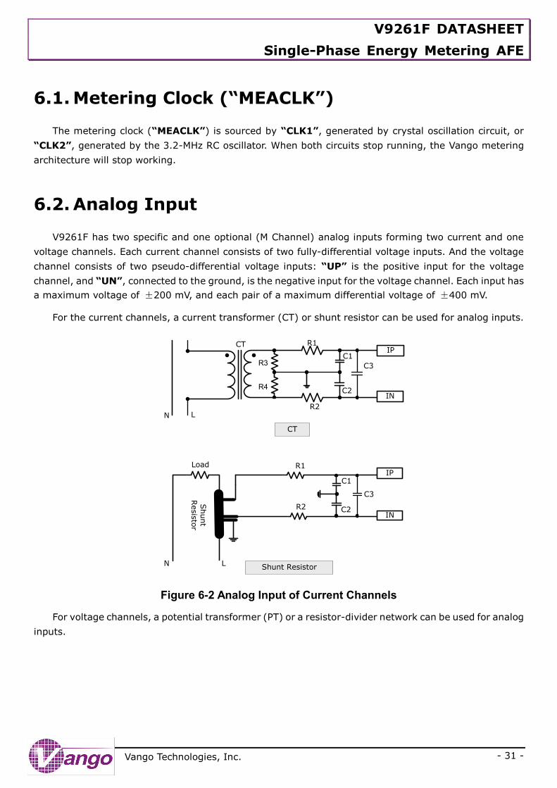
V9261F has two specific and one optional (M Channel) analog inputs forming two current and one
voltage channels. Each current channel consists of two fully-differential voltage inputs. And the voltage
channel consists of two pseudo-differential voltage inputs: “UP” is the positive input for the voltage
channel, and “UN”, connected to the ground, is the negative input for the voltage channel. Each input has
a maximum voltage of ±200 mV, and each pair of a maximum differential voltage of ±400 mV.
For the current channels, a current transformer (CT) or shunt resistor can be used for analog inputs.
IP
IN
LN
CT R1
R2
R3
CT
Shunt ResistorN L
Shunt
Resis
tor
R2
R1LoadIP
IN
C1
C2
C3
C1
C2
C3
R4
Figure 6-2 Analog Input of Current Channels
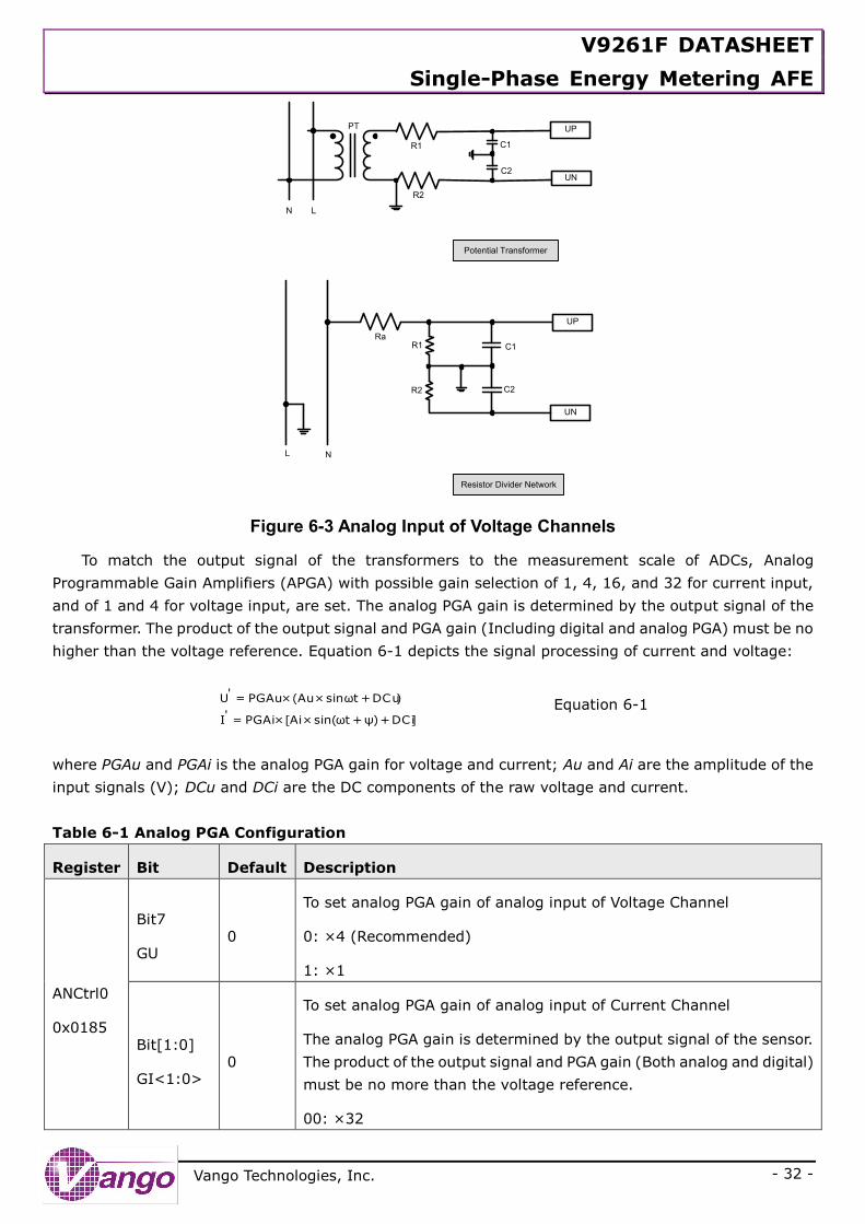
For voltage channels, a potential transformer (PT) or a resistor-divider network can be used for analog
inputs.
V9261F DATASHEET
Single-Phase Energy Metering AFE
- 32 -
Vango Technologies, Inc.
R1
PT
N L
Ra
Potential Transformer
Resistor Divider Network
UP
UN
C1
C2
UP
UN
C1
C2
R1
R2
R2
NL
Figure 6-3 Analog Input of Voltage Channels
To match the output signal of the transformers to the measurement scale of ADCs, Analog
Programmable Gain Amplifiers (APGA) with possible gain selection of 1, 4, 16, and 32 for current input,
and of 1 and 4 for voltage input, are set. The analog PGA gain is determined by the output signal of the
transformer. The product of the output signal and PGA gain (Including digital and analog PGA) must be no
higher than the voltage reference. Equation 6-1 depicts the signal processing of current and voltage:
]DCi+)ψ+tωsin(×Ai[×PGAi='I
)DCu+tωsin×Au(×PGAu='U Equation 6-1
where PGAu and PGAi is the analog PGA gain for voltage and current; Au and Ai are the amplitude of the
input signals (V); DCu and DCi are the DC components of the raw voltage and current.
Table 6-1 Analog PGA Configuration
Register Bit Default Description
ANCtrl0
0x0185
Bit7
GU 0
To set analog PGA gain of analog input of Voltage Channel
0: ×4 (Recommended)
1: ×1
Bit[1:0]
GI<1:0> 0
To set analog PGA gain of analog input of Current Channel
The analog PGA gain is determined by the output signal of the sensor.
The product of the output signal and PGA gain (Both analog and digital)
must be no more than the voltage reference.
00: ×32
V9261F DATASHEET
Single-Phase Energy Metering AFE
- 33 -
Vango Technologies, Inc.
Register Bit Default Description
01: ×16
10: ×4
11: ×1
bit[5:4]
GM<1:0> 0
M-channel ADC analog gain control
Users should confirm PGA according to the output signal of sensor and
make sure the product of the biggest signal and PGA is smaller than
the bandgap voltage.
00: ×4
01: ×1
10: ×32
11: ×16
6.3. Analog-to-Digital Conversion
Second-order Σ-ΔADCs are applied in the voltage and current channels in V9261F. Σ-ΔADCs can be
enabled or disabled via configuring the “ANCtrl0” register (0x0185).
Table 6-2 Enable/Disable ADCs of Each Channel
Register Bit Default Description
ANCtrl0
0x0185
Bit26
ADCUPDN 0
Set this bit to ‘1’ to enable Voltage Channel ADC. The BandGap circuit
must be enabled before this ADC.
Both in the Sleep Mode and in Current Detection Mode, this bit is
cleared automatically.
Bit24
ADCIPDN 0
Set this bit to ‘1’ to enable Current Channel ADC. The BandGap circuit
must be enabled before this ADC.
In the Sleep Mode, this bit is cleared automatically. In the Current
Detection Mode, this bit is set to ‘1’ automatically.
bit25
ADCMPDN 0
To set this bit to ‘1’ to enable M channel ADC
Before enabling ADC, the BandGap circuit must be enabled first. By
default M channel ADC is disabled.
No matter in the Sleep Mode or Current Detection mode, M channel
ADC is disabled automatically.
The sampling frequency of ADCs, or ADC clock (“ADCCLK”), is derived from “CLK1”. By default, it is
819.2 kHz, a quarter of the metering clock (“MEACLK”), and can be adjusted via “bit[17:16]” of
V9261F DATASHEET
Single-Phase Energy Metering AFE
- 34 -
Vango Technologies, Inc.
“ANCtrl0” (0x0185).
Table 6-3 Configuring ADCCLK
Register Bit Description
ANCtrl0
0x0185
Bit[17:16]
ADCLKSEL<1:0>
To select the sampling frequency of the oversampling ADC (ADC clock,
“ADCCLK”). The sampling frequency of ADCs must be a quarter or one
eighth of the metering clock (“MEACLK”) frequency when the chip
operates with full functions in the Metering Mode.
00: 819.2 kHz
01: 409.6 kHz
10: 204.8 kHz
11: 102.4 kHz
In the Current Detection Mode, these bits must be set to “0b10” to lower
the power dissipation.
When the chip operates with full functions in the Metering Mode, their
default values are recommended to be used for the best performance.
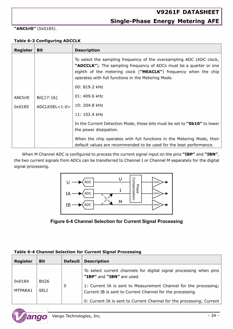
When M Channel ADC is configured to process the current signal input on the pins “IBP” and “IBN”,
the two current signals from ADCs can be transferred to Channel I or Channel M separately for the digital
signal processing.
U
IA
IB
I
M
UADC
ADC
ADC
Phase
Com
pensatio
n
DPGA
DPGA
DPGA
Figure 6-4 Channel Selection for Current Signal Processing
Table 6-4 Channel Selection for Current Signal Processing
Register Bit Default Description
0x0184
MTPARA1
Bit26
SELI 0
To select current channels for digital signal processing when pins
“IBP” and “IBN” are used.
1: Current IA is sent to Measurement Channel for the processing;
Current IB is sent to Current Channel for the processing.
0: Current IA is sent to Current Channel for the processing; Current
V9261F DATASHEET
Single-Phase Energy Metering AFE
- 35 -
Vango Technologies, Inc.
Register Bit Default Description
IB is sent to Measurement Channel for the processing.
The signal output from ADCs must be input to a phase compensation circuit to correct the phase error
between the current and voltage signal introduced by the mismatch of the transformers and ADCs.
6.4. Phase Compensation
A phase compensation circuit composed of a chain of time-delay units is applied to correct the phase
error between the current and voltage signals. Either the current or voltage signal can be selected to be
delayed via the bit “PHCIU” (“bit18” of “MTPARA1”, 0x0184). The phase compensation resolution is
0.0055°/lsb, and the maximum phase error correction range is ±1.4°.
Table 6-5 Registers for phase compensation
Register Bit Default Description
MTPARA1
0x0184
Bit19
ENPHC 0
Set this bit to ‘1’ to enable phase compensation.
By default this function is disabled.
Bit18
PHCIU 0
Set this bit to ‘1’ to delay voltage for phase compensation.
Clear this bit to delay current for phase compensation.
Bit[15:8]
PHC 0
To set the absolute value for phase compensation.
By default the resolution is 0.0055°/lsb, and a phase error of up to 1.4°
can be calibrated.
U
I
PH
C_
U_
I
Time-delay circuit
PH
C_
U_
I
U
I
Figure 6-5 Phase Compensation
Compensate the phase error at power factor of 0.5L:
)819200
fsmpl×E×
2
3011(Round=N
Equation 6-2
where
N is the value to be set in bit[15:8] of register MTPARA1 (0x0184);
E is the error displayed in LCD screen of the calibration equipment.
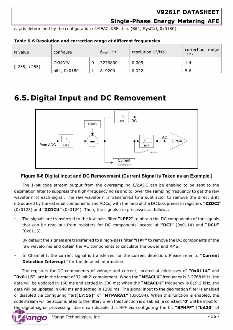
V9261F DATASHEET
Single-Phase Energy Metering AFE
- 36 -
Vango Technologies, Inc.
fsmpl is determined by the configuration of MEACLKSEL bits (Bit1, SysCtrl, 0x0180).
Table 6-6 Resolution and correction range at different frequencies
N value configure fsmpl(Hz) resolution(°/lsb) correction range
(°)
[-255, +255] CKMDIV
bit1, 0x0180
0 3276800 0.005 1.4
1 819200 0.022 5.6
6.5. Digital Input and DC Removement
-
BIAS
from ADC
Current
detection
AC
DC
DPGALPF1
LPF2
HPF
Figure 6-6 Digital Input and DC Removement (Current Signal is Taken as an Example.)
The 1-bit code stream output from the oversampling Σ/ΔADC can be enabled to be sent to the
decimation filter to suppress the high-frequency noise and to lower the sampling frequency to get the raw
waveform of each signal. The raw waveform is transferred to a subtractor to remove the direct drift
introduced by the external components and ADCs, with the help of the DC bias preset in registers “ZZDCI”
(0x0123) and “ZZDCU” (0x0124). Then, the signals are processed as follows:
- The signals are transferred to the low-pass filter “LPF2” to obtain the DC components of the signals
that can be read out from registers for DC components located at “DCI” (0x0114) and “DCU”
(0x0115).
- By default the signals are transferred to a high-pass filter “HPF” to remove the DC components of the
raw waveforms and obtain the AC components to calculate the power and RMS.
- In Channel I, the current signal is transferred for the current detection. Please refer to “Current
Detection Interrupt” for the detailed information.
The registers for DC components of voltage and current, located at addresses of “0x0114” and
“0x0115”, are in the format of 32-bit 2’ complement. When the “MEACLK” frequency is 3.2768 MHz, the
data will be updated in 160 ms and settled in 300 ms; when the “MEACLK” frequency is 819.2 kHz, the
data will be updated in 640 ms and settled in 1200 ms. The signal input to the decimation filter is enabled
or disabled via configuring “bit[17:16]” of “MTPARA1” (0x0184). When this function is enabled, the
code stream will be accumulated to the filter; when this function is disabled, a constant ‘0’ will be input for
the digital signal processing. Users can disable this HPF via configuring the bit “BPHPF” (“bit20” of
V9261F DATASHEET
Single-Phase Energy Metering AFE
- 37 -
Vango Technologies, Inc.
“MTPARA1”, 0x0184).
Table 6-7 Enable/Disable Digital Inputs
Register Bit Description
MTPARA1
0x0184
Bit17
ONI
To enable digital signal input of current channel for digital signal processing
1: Enable.
0: Disable. When this bit is cleared, a constant ‘0’ is input for digital signal processing.
Bit16
ONU
To enable digital signal input of voltage channel for digital signal processing
1: Enable
0: Disable. When this bit is cleared, a constant ‘0’ will be input for the digital signal
processing.
Digital Programmable Gain Amplifiers (DPGA) with possible gain selection of 1/32~32, via
“MTPARA1” (0x0184), are applied to digital signals output from the high-pass filter to amplify the
signals. The product of the signal and PGA gains (Including digital and analog PGA) must be no higher
than the voltage reference.
Table 6-8 DPGA Gain Selection for Digital Signals
Register Bit Default Description
MTPARA1
0x0184
Bit[7:4]
PGAI 0
To set digital PGA gain of current input
0000: ×1; 0001: ×1/2; 0010: ×1/4; 0011: ×1/8; 0100: ×1/16; 0101:
×1/32;
1000: ×1; 1001: ×2; 1010: ×4; 1011: ×8; 1100: ×16; 1101: ×32.
Bit[3:0]
PGAU 0
To set digital PGA gain of voltage input
0000: ×1; 0001: ×1/2; 0010: ×1/4; 0011: ×1/8; 0100: ×1/16; 0101:
×1/32;
1000: ×1; 1001: ×2; 1010: ×4; 1011: ×8; 1100: ×16; 1101: ×32.
Equation 6-3 depicts the signal processing:
188.1
)φ+tωsin(×Ai×PGAi×PGAdi=I
188.1
tωsin×Au×PGAu×PGAdu=U
Equation 6-3
Where,
PGAdu and PGAdi are the DPGA gains.
PGAu and PGAi are the APGA gains.
Au and Ai are the amplitude of current and voltage inputs.
1.188 is the reference voltage.
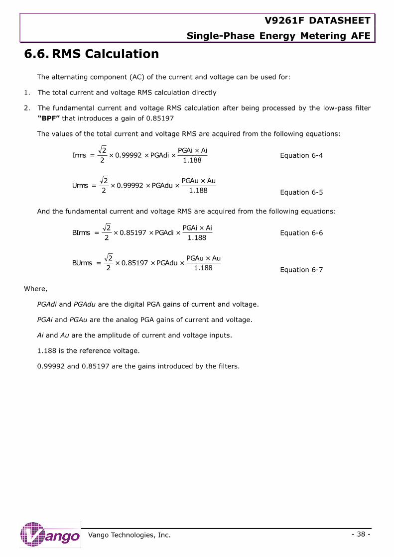
V9261F DATASHEET
Single-Phase Energy Metering AFE
- 38 -
Vango Technologies, Inc.
6.6. RMS Calculation
The alternating component (AC) of the current and voltage can be used for:
1. The total current and voltage RMS calculation directly
2. The fundamental current and voltage RMS calculation after being processed by the low-pass filter
“BPF” that introduces a gain of 0.85197
The values of the total current and voltage RMS are acquired from the following equations:
188.1
Ai×PGAi×PGAdi×0.99992×
2
2=Irms Equation 6-4
188.1
Au×PGAu×PGAdu×0.99992×
2
2=Urms
Equation 6-5
And the fundamental current and voltage RMS are acquired from the following equations:
188.1
Ai×PGAi×PGAdi×0.85197×
2
2=BIrms Equation 6-6
188.1
Au×PGAu×PGAdu×0.85197×
2
2=BUrms
Equation 6-7
Where,
PGAdi and PGAdu are the digital PGA gains of current and voltage.
PGAi and PGAu are the analog PGA gains of current and voltage.
Ai and Au are the amplitude of current and voltage inputs.
1.188 is the reference voltage.
0.99992 and 0.85197 are the gains introduced by the filters.
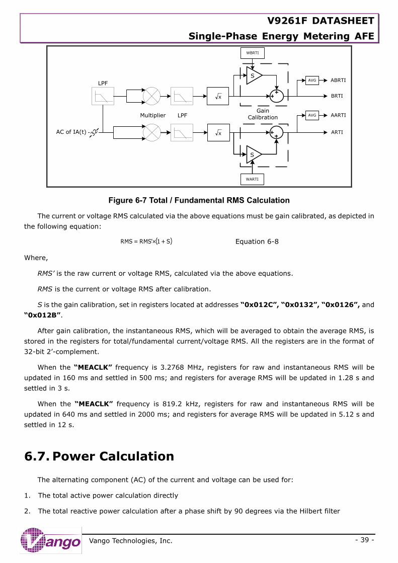
V9261F DATASHEET
Single-Phase Energy Metering AFE
- 39 -
Vango Technologies, Inc.
LPFMultiplierGain
Calibration
AC of IA(t)
S
32
WARTI
LPF
S
WBRTI
ARTI
BRTIx
x
AVG
AVG
ABRTI
AARTI
Figure 6-7 Total / Fundamental RMS Calculation
The current or voltage RMS calculated via the above equations must be gain calibrated, as depicted in
the following equation:
( )S+1×’RMS=RMS Equation 6-8
Where,
RMS’ is the raw current or voltage RMS, calculated via the above equations.
RMS is the current or voltage RMS after calibration.
S is the gain calibration, set in registers located at addresses “0x012C”, “0x0132”, “0x0126”, and
“0x012B”.
After gain calibration, the instantaneous RMS, which will be averaged to obtain the average RMS, is
stored in the registers for total/fundamental current/voltage RMS. All the registers are in the format of
32-bit 2’-complement.
When the “MEACLK” frequency is 3.2768 MHz, registers for raw and instantaneous RMS will be
updated in 160 ms and settled in 500 ms; and registers for average RMS will be updated in 1.28 s and
settled in 3 s.
When the “MEACLK” frequency is 819.2 kHz, registers for raw and instantaneous RMS will be
updated in 640 ms and settled in 2000 ms; and registers for average RMS will be updated in 5.12 s and
settled in 12 s.
6.7. Power Calculation
The alternating component (AC) of the current and voltage can be used for:
1. The total active power calculation directly
2. The total reactive power calculation after a phase shift by 90 degrees via the Hilbert filter
V9261F DATASHEET
Single-Phase Energy Metering AFE
- 40 -
Vango Technologies, Inc.
And after being processed by the low-pass filter, the current and voltage signal are used to compute
the fundamental active and reactive power.
LPFMultiplier Gain Calibration
AC of IA(t)
AC of UA(t)
S
32
32
WAPT
LPFS
WBPT
LPFMultiplier Gain Calibration
AC of IA(t)
AC of UA(t)
S
32
32
WAQT
LPFS
WBQT
Phase s
hift
90˚
IBP
IAP
IBQ
IAQ
Offset Cali
Offset Cali
Offset Cali
Offset Cali
AVG
AVG
AVG
AVG
WWBQT
WWAQT
WWAPT
WWBPT
Total/Fundamental Active Power
Total/Fundamental Reactive Power
ABP
AAP
ABQ
AAQ
Figure 6-8 Active/Reactive Power Calculation
The total signals, including fundamental wave and harmonic wave, are used to calculate the total
active and reactive power directly. The active power is acquired via the following equation:
99985.0×θcos×188.1
PGAdu×PGAu×Au×
188.1
PGAdi×PGAi×Ai×
2
1=P Equation 6-9
And the reactive power is acquired via the following equation:
78402.0×θsin×188.1
PGAdu×PGAu×Au×
188.1
PGAdi×PGAi×Ai×
2
1=Q Equation 6-10
Where,
PGAdi and PGAdu are digital PGA gains of current and voltage.
PGAi and PGAu are analog PGA gains of current and voltage.
Ai and Au are the amplitude of current and voltage inputs.
θ is the phase difference between voltage and current signals.
V9261F DATASHEET
Single-Phase Energy Metering AFE
- 41 -
Vango Technologies, Inc.
0.99985 and 0.78402 are the gains introduced by the filters.
Filtered by the band-pass filter, the signals are used to calculate the fundamental active and reactive
power.
Fundamental active power: 72585.0×θcos×188.1
PGAdu×PGAu×Au×
188.1
PGAdi×PGAi×Ai×
2
1=BP Equation
6-11
Fundamental reactive power: 36292.0×θsin×188.1
PGAdu×PGAu×Au×
188.1
PGAdi×PGAi×Ai×
2
1=BQ Equation 6-12
Where,
PGAdi and PGAdu are digital PGA gains of current and voltage.
PGAi and PGAu are analog PGA gains of current and voltage.
Ai and Au are the amplitude of current and voltage inputs.
θ is the phase difference between voltage and current signals.
0.72585 and 0.36292 are the gains introduced by the filters.
The active or reactive power must be gain and offset calibrated, as depicted in the following equation,
( ) C+S+1×’P=P Equation 6-13
Where,
P’ is the raw active or reactive power calculated via the above equations.
P is the active or reactive power after calibration.
S is the gain calibration set in the registers.
C is the offset calibration set in the registers.
After gain and offset calibration, the instantaneous active and reactive power, which will be averaged
to obtain the average active and reactive power, is stored in the total and fundamental active/reactive
power registers. All the registers are in the format of 32-bit 2’-complement.
When the “MEACLK” frequency is 3.2768 MHz, registers for the raw and instantaneous power will be
updated in 160 ms and settled in 500 ms; and registers for the average power will be updated in 1.28 s
and settled in 3 s.
When the “MEACLK” frequency is 819.2 kHz, registers for the raw and instantaneous power will be
updated in 640 ms and settled in 2000 ms; and registers for the average power will be updated in 5.12 s
and settled in 12 s.
6.8. Energy Accumulation and CF Pulse Output
V9261F supports the energy accumulation and converting the energy into pulses. By default this
function is disabled. Users can set the bit “EGYEN” (“bit30” of “MTPARA0”, 0x0183) to ‘1’ to enable
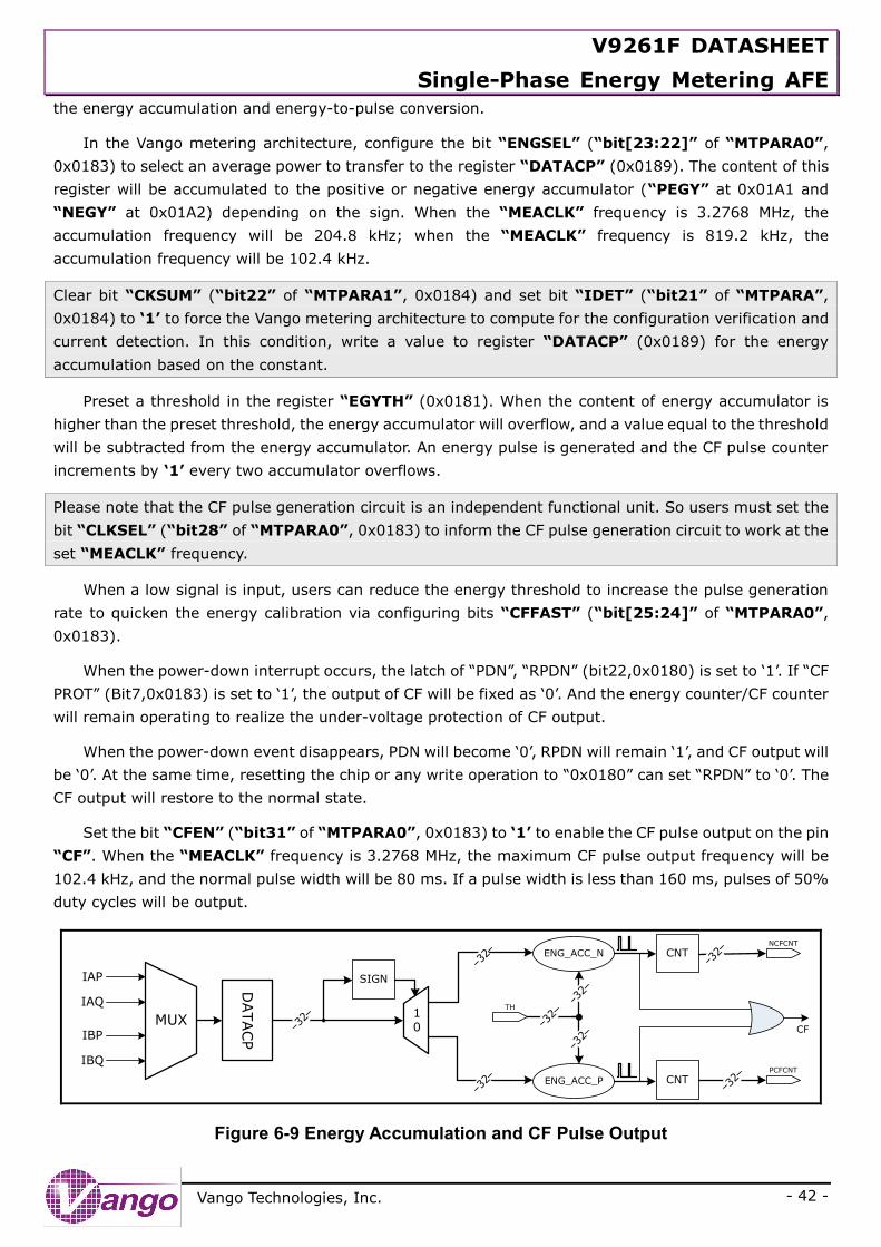
V9261F DATASHEET
Single-Phase Energy Metering AFE
- 42 -
Vango Technologies, Inc.
the energy accumulation and energy-to-pulse conversion.
In the Vango metering architecture, configure the bit “ENGSEL” (“bit[23:22]” of “MTPARA0”,
0x0183) to select an average power to transfer to the register “DATACP” (0x0189). The content of this
register will be accumulated to the positive or negative energy accumulator (“PEGY” at 0x01A1 and
“NEGY” at 0x01A2) depending on the sign. When the “MEACLK” frequency is 3.2768 MHz, the
accumulation frequency will be 204.8 kHz; when the “MEACLK” frequency is 819.2 kHz, the
accumulation frequency will be 102.4 kHz.
Clear bit “CKSUM” (“bit22” of “MTPARA1”, 0x0184) and set bit “IDET” (“bit21” of “MTPARA”,
0x0184) to ‘1’ to force the Vango metering architecture to compute for the configuration verification and
current detection. In this condition, write a value to register “DATACP” (0x0189) for the energy
accumulation based on the constant.
Preset a threshold in the register “EGYTH” (0x0181). When the content of energy accumulator is
higher than the preset threshold, the energy accumulator will overflow, and a value equal to the threshold
will be subtracted from the energy accumulator. An energy pulse is generated and the CF pulse counter
increments by ‘1’ every two accumulator overflows.
Please note that the CF pulse generation circuit is an independent functional unit. So users must set the
bit “CLKSEL” (“bit28” of “MTPARA0”, 0x0183) to inform the CF pulse generation circuit to work at the
set “MEACLK” frequency.
When a low signal is input, users can reduce the energy threshold to increase the pulse generation
rate to quicken the energy calibration via configuring bits “CFFAST” (“bit[25:24]” of “MTPARA0”,
0x0183).
When the power-down interrupt occurs, the latch of “PDN”, “RPDN” (bit22,0x0180) is set to ‘1’. If “CF
PROT” (Bit7,0x0183) is set to ‘1’, the output of CF will be fixed as ‘0’. And the energy counter/CF counter
will remain operating to realize the under-voltage protection of CF output.
When the power-down event disappears, PDN will become ‘0’, RPDN will remain ‘1’, and CF output will
be ‘0’. At the same time, resetting the chip or any write operation to “0x0180” can set “RPDN” to ‘0’. The
CF output will restore to the normal state.
Set the bit “CFEN” (“bit31” of “MTPARA0”, 0x0183) to ‘1’ to enable the CF pulse output on the pin
“CF”. When the “MEACLK” frequency is 3.2768 MHz, the maximum CF pulse output frequency will be
102.4 kHz, and the normal pulse width will be 80 ms. If a pulse width is less than 160 ms, pulses of 50%
duty cycles will be output.
ENG_ACC_N CNT
ENG_ACC_P CNT
TH
NCFCNT
PCFCNT
10
SIGN
32
32
32
32
IAP
32
32
IAQ
IBP
IBQ
MUX
32
32
CF
DATACP
Figure 6-9 Energy Accumulation and CF Pulse Output
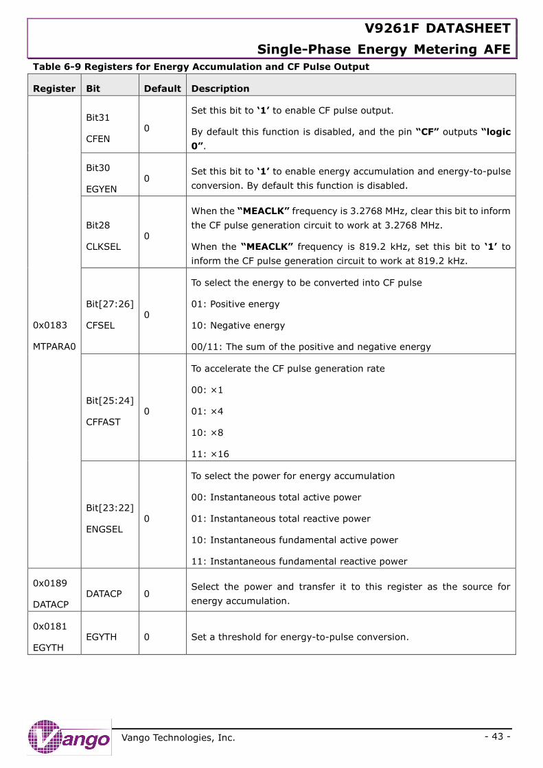
V9261F DATASHEET
Single-Phase Energy Metering AFE
- 43 -
Vango Technologies, Inc.
Table 6-9 Registers for Energy Accumulation and CF Pulse Output
Register Bit Default Description
0x0183
MTPARA0
Bit31
CFEN 0
Set this bit to ‘1’ to enable CF pulse output.
By default this function is disabled, and the pin “CF” outputs “logic
0”.
Bit30
EGYEN 0
Set this bit to ‘1’ to enable energy accumulation and energy-to-pulse
conversion. By default this function is disabled.
Bit28
CLKSEL 0
When the “MEACLK” frequency is 3.2768 MHz, clear this bit to inform
the CF pulse generation circuit to work at 3.2768 MHz.
When the “MEACLK” frequency is 819.2 kHz, set this bit to ‘1’ to
inform the CF pulse generation circuit to work at 819.2 kHz.
Bit[27:26]
CFSEL 0
To select the energy to be converted into CF pulse
01: Positive energy
10: Negative energy
00/11: The sum of the positive and negative energy
Bit[25:24]
CFFAST 0
To accelerate the CF pulse generation rate
00: ×1
01: ×4
10: ×8
11: ×16
Bit[23:22]
ENGSEL 0
To select the power for energy accumulation
00: Instantaneous total active power
01: Instantaneous total reactive power
10: Instantaneous fundamental active power
11: Instantaneous fundamental reactive power
0x0189
DATACP DATACP 0
Select the power and transfer it to this register as the source for
energy accumulation.
0x0181
EGYTH EGYTH 0 Set a threshold for energy-to-pulse conversion.
V9261F DATASHEET
Single-Phase Energy Metering AFE
- 44 -
Vango Technologies, Inc.
6.9. No-Load Detection
V9261F supports the no-load detection. By default this function is disabled, but users can enable it via
configuring the bit “CRPEN” (“bit29” of “MTPARO0”, 0x0183).
There is an anti-creeping accumulator in the no-load detection circuit. When the no-load detection is
enabled, 1s will be accumulated in this accumulator constantly at the same frequency of the energy
accumulation.
When the no-load detection is enabled, the constant 1s will be accumulated into the embedded
anti-creeping accumulator, and the energy accumulators will accumulate the content of register
“DATACP” (0x0189). Preset a threshold for the no-load detection in the register “CTH” (0x0182), and a
threshold for energy-to-pulse conversion in the register “EGYTH” (0x0181). Compare the accumulation
rate. If the energy accumulator overflows sooner, the anti-creeping accumulator will be cleared, and the
Vango metering architecture will start to meter the energy. Otherwise, the Vango metering architecture
will enter the creeping state. Users can read the bit “CFCRP” (“bit31” of “SysCtrl”, 0x0180) to detect
the state.
The threshold register for the no-load detection are of actual 32-bit length. It will be padded with a
string of 4 0s on the right to work as a 36-bit register.
Table 6-10 Registers and Bits for No-Load Detection
Register Bit Default Description
0x0183
MTPARA0
Bit29
CRPEN 0
Set this bit to ‘1’ to enable no-load detection.
By default this function is disabled.
0x0180
SysCtrl
Bit31
CFCRP 0
To indicate the state of the system
0: Metering energy
1: Creeping
0x0182
CTH 0 Set a threshold for no-load detection.
6.10. Line Frequency Measurement
V9261F supports the line frequency measurement.
In the line frequency measurement circuit, the fundamental voltage signal is sampled at a frequency
of 3200 Hz for the negative-to-positive zero-crossing detection, and the number of the samples among
two continuous negative-to-positive transitions is equal to the instantaneous line frequency. So the
instantaneous line frequency is calculated as follows:
FREQ
3200=f Equation 6-14
V9261F DATASHEET
Single-Phase Energy Metering AFE
- 45 -
Vango Technologies, Inc.
Where, f is the line frequency to be measured; FREQ is the content of the instantaneous line frequency
register (0x019A), in the form of decimal.
The instantaneous line frequency will be accumulated 256 times every 1.28 s to be averaged to
acquire the average line frequency per second:
ASFREQ
256×3200='f Equation 6-15
Where, f’ is the line frequency to be measured; ASFREQ is the average line frequency per second read out
of the register (0x011D), in the form of decimal.
To improve the measurement accuracy, the above average line frequency per second will be
accumulated 8 times every 10.24 s to be averaged to acquire the average line frequency:
AFREQ
8×256×3200=''f Equation 6-16
Where, f’’ is the line frequency to be measured; AFREQ is the average line frequency read out of the
register (0x011E), in the form of decimal.
In V9261F, a band-pass filter is applied to remove the direct component, the noise and the harmonic
wave of the voltage signal to obtain the fundamental voltage for line frequency measurement. The
performance of the band-pass filter is affected by the number of bits to be shifted and the filter coefficient.
When fewer bits are shifted, the filter needs less time to respond, is less sensitive to the frequency
deviation, and has less capability to depress the noise and harmonics.
Table 6-11 Bandpass Filter Parameters
Group
Shift bits (0x0183, MTPARA0) Bandpass filter
coefficient Frequency deviation
BPFSFT,
bit[14:13]
Bits to be
shifted BPFPARA, 0x0125 47.5Hz(db) 150Hz(db)
0 00 >>8 0x811D2BA7 -4.2 -30.5
1 01 >>9 0x80DD7A8C -8.9 -36.5
2 10 >>10 0x80BDA1FE -14.1 -42.6
3 11 >>11 0x80ADB5B8 -20 -48.6
Generally, Group 0 is preferred.
6.11. Measuring Various Signals in M Channel
The M Channel can be used to measure the current, ground, and temperature. As illustrated in
Figure 6-10, there is only one ADC in the M Channel, so users must configure registers to use this channel
to measure one signal at a time.
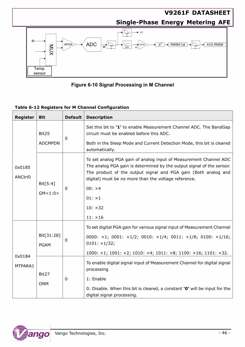
V9261F DATASHEET
Single-Phase Energy Metering AFE
- 46 -
Vango Technologies, Inc.
MU
X
ADCM
X2 RMSM Cal AVG RMSMAPGA
IB
Temp.
sensor
LP
FHPF
LP
F
DPGA
AC
DC
LP
F
Figure 6-10 Signal Processing in M Channel
Table 6-12 Registers for M Channel Configuration
Register Bit Default Description
0x0185
ANCtrl0
Bit25
ADCMPDN 0
Set this bit to ‘1’ to enable Measurement Channel ADC. The BandGap
circuit must be enabled before this ADC.
Both in the Sleep Mode and Current Detection Mode, this bit is cleared
automatically.
Bit[5:4]
GM<1:0> 0
To set analog PGA gain of analog input of Measurement Channel ADC
The analog PGA gain is determined by the output signal of the sensor.
The product of the output signal and PGA gain (Both analog and
digital) must be no more than the voltage reference.
00: ×4
01: ×1
10: ×32
11: ×16
0x0184
MTPARA1
Bit[31:28]
PGAM 0
To set digital PGA gain for various signal input of Measurement Channel
0000: ×1; 0001: ×1/2; 0010: ×1/4; 0011: ×1/8; 0100: ×1/16;
0101: ×1/32;
1000: ×1; 1001: ×2; 1010: ×4; 1011: ×8; 1100: ×16; 1101: ×32.
Bit27
ONM 0
To enable digital signal input of Measurement Channel for digital signal
processing
1: Enable
0: Disable. When this bit is cleared, a constant ‘0’ will be input for the
digital signal processing.
V9261F DATASHEET
Single-Phase Energy Metering AFE
- 47 -
Vango Technologies, Inc.
Register Bit Default Description
Bit26
SELI 0
To select current channels for digital signal processing when pins
“IBP” and “IBN” are used
1: Current IA is sent to Measurement Channel for processing; current
IB is sent to Current Channel for processing.
0: Current IA is sent to Current Channel for processing; Current IB is
sent to Measurement Channel for processing.
Bit25
CIB 0
Set this bit to ‘1’ to enable digital signal processing in Measurement
Channel.
By default this function is disabled.
0x0180
SysCtrl
Bit[7:5]
MEAS 0
To select the analog input for signal processing in Measurement
Channel ADC.
000: Current input on pins “IBP”/“IBN”
001/010/011: Reserved
100: Temperature
101/110/111: Ground
0x0186
ANCtrl1
Bit[22:20]
MEAS 0
To select the analog input for signal processing in Measurement
Channel ADC
000: Current input on pins “IBP”/“IBN”
001/010/011: Reserved
100: Temperature
101/110/111: Ground
The setting of “bit[22:20]” must match the “MEAS” (Bit[7:5])
setting in “SysCtrl” (0x0180).
Table 6-13 Data Registers for M Channel
Register Description
0x0116 DCM
The DC component of various signals processed in M Channel
When the “MEACLK” frequency is 3.2768 MHz, this register will be updated in 160
ms, and settled in 300 ms.
When the “MEACLK” frequency is 819.2 kHz, this register will be updated in 640
ms and settled in 1200 ms.
V9261F DATASHEET
Single-Phase Energy Metering AFE
- 48 -
Vango Technologies, Inc.
Register Description
0x00F9 DCIM
When the M Channel is used to process the current signal input from pins
“IBP”/“IBN” or “IAP”/“IAN”, this register “DCM” (0x0116) will be the backup
of the content of register “DCM” (0x0116), and the master MCU should read this
register for the measurement.
0x0101 DCTM
When Measurement Channel (M) is used to measure temperature, this register will
be the backup of the content of register “DCM” (0x0116), and the master MCU
should read this register for the measurement.
0x0106 ARRTM
The raw RMS value of the various signal of Measurement Channel
When the “MEACLK” frequency is 3.2768 MHz, the register will be updated in
160 ms and settled in 500 ms. When the “MEACLK” frequency is 819.2 kHz, the
register will be updated in 640 ms and settled in 2000 ms.
0x010F ARTM
The instantaneous RMS value of the various signal of Measurement Channel
When the “MEACLK” frequency is 3.2768 MHz, the register will be updated in
160 ms and settled in 500 ms. When the “MEACLK” frequency is 819.2 kHz, the
register will be updated in 640 ms and settled in 2000 ms.
0x00F8 ARTIM
When Measurement Channel (M) is used to process the current signal input from
pins “IBP”/“IBN” or “IAP”/“IAN”, this register will be the backup of the content
of register “ARTM” (0x010F), and the master MCU should read this register for the
measurement.
0x0100 ARTMM
When Measurement Channel (M) is used to measure temperature, this register will
be the backup of the content of register “ARTM” (0x010F), and the master MCU
should read this register for the measurement.
0x0117 AARTM
The average RMS value of the various signal of Measurement Channel
When the “MEACLK” frequency is 3.2768 MHz, the register will be updated in
1.28 s and settled in 3 s. When the “MEACLK” frequency is 819.2 kHz, the register
will be updated in 5.12 s and settled in 12 s.
6.12. Calibration
6.12.1. Registers for Meter Calibration
Table 6-14 Registers for Meter Calibration
Address Register R/W Format
0x011B AARTU The average total voltage RMS R/W 32-bit 2’-complement
0x011C AARTI The average total current RMS R/W 32-bit 2’-complement
V9261F DATASHEET
Single-Phase Energy Metering AFE
- 49 -
Vango Technologies, Inc.
Address Register R/W Format
0x0121 ABRTU The average fundamental voltage RMS R/W 32-bit 2’-complement
0x0122 ABRTI The average fundamental current RMS R/W 32-bit 2’-complement
0x0119 AAP The average total active power R/W 32-bit 2’-complement
0x011A AAQ The average total reactive power R/W 32-bit 2’-complement
0x011F ABP The average fundamental active power R/W 32-bit 2’-complement
0x0120 ABQ The average fundamental reactive power R/W 32-bit 2’-complement
0x012C WARTI Set a value to gain calibrate the total current RMS. R/W 32-bit 2’-complement
0x0132 WARTU Set a value to gain calibrate the total voltage RMS. R/W 32-bit 2’-complement
0x0126 WBRTI Set a value to gain calibrate the fundamental
current RMS. R/W 32-bit 2’-complement
0x012B WBRTU Set a value to gain calibrate the fundamental
voltage RMS. R/W 32-bit 2’-complement
0x012E WAPT Set a value to gain calibrate the total active power. R/W 32-bit 2’-complement
0x0130 WAQT Set a value to gain calibrate the total reactive
power. R/W 32-bit 2’-complement
0x012F WWAPT Set a value to offset calibrate the total active power. R/W 32-bit 2’-complement
0x0131 WWAQT Set a value to offset calibrate the total reactive
power. R/W 32-bit 2’-complement
0x0127 WBPT Set a value to gain calibrate the fundamental active
power. R/W 32-bit 2’-complement
0x0129 WBQT Set a value to gain calibrate the fundamental
reactive power. R/W 32-bit 2’-complement
0x0128 WWBPT Set a value to offset calibrate the fundamental
active power. R/W 32-bit 2’-complement
0x012A WWBQT Set a value to offset calibrate the fundamental
reactive power. R/W 32-bit 2’-complement
0x0181 EGYTH Set a threshold for energy-to-pulse conversion. R/W 32-bit 2’-complement
0x0182 CTH Set a threshold for no-load detection. R/W 32-bit 2’-complement
0x0117 AARTM
The average current RMS value of the various signal
of M Channel when it is used for current
measurement
R/W 32-bit 2’-complement
0x012D WARTM Set a value to gain calibrate the RMS value of
various signal in M Channel. R/W 32-bit 2’-complement
V9261F DATASHEET
Single-Phase Energy Metering AFE
- 50 -
Vango Technologies, Inc.
6.12.2. Equations for Calibration
1. Equation for current/voltage RMS registers
K×G×V=Value Equation 6-17
Where, V is the RMS value of the input signal; G is the gain; and K is a coefficient, 1.486×10⁹ for
fundamental RMS and 1.745×10⁹ for total RMS.
2. Equation for active power registers.
θcos×pB×Gv×Vv×Gi×Vi=P Equation 6-18
Where, Vi and Vv are the input current and voltage; Gi and Gv are the analog PGA gains for current and
voltage respectively; cosθ is the power factor; Bp is a coefficient, 1.419×10⁹ for total active power and
1.030×10⁹ for fundamental active power.
3. Equation for reactive power registers
θins×qB×Gv×Vv×Gi×Vi=Q Equation 6-19
Where, Vi and Vv are the input current and voltage; Gi and Gv are the analog PGA gains for current and
voltage respectively; θ is phase difference between current and voltage; Bq is a coefficient, 1.111×10⁹ for
total reactive power and 0.514×10⁹ for fundamental reactive power.
4. Equation for ratio of RMS and power
The value acquired by Equation 6-17, Equation 6-18, or Equation 6-19 is the theoretical value of the
register of RMS or power. It must be multiplied by a ratio to get the actual value (Accurate to the second
decimal place).
ValuenV=D Equation 6-20
Where, Value is the theoretical value of the registers acquired by Equation 6-17, Equation 6-18, or
Equation 6-19; D is the ratio; and Vn is the rated voltage/current/power.
5. Equation for registers for phase compensation
Compensate the phase error at power factor of 0.5L:
)819200
fsmpl×E×
2
3011(Round=N
Equation 6-21
Where
N is the value to be set in bit[15:8] of register MTPARA1 (0x0184);
E is the error displayed in LCD screen of the calibration equipment.
fsmpl is determined by the configuration of MEACLKSEL bits (Bit1, SysCtrl, 0x0180).
V9261F DATASHEET
Single-Phase Energy Metering AFE
- 51 -
Vango Technologies, Inc.
6. Equation for energy pulse conversion threshold
25.6×T×'P=142
204800×
2
1×T×'P=PGAT Equation 6-22
Where, P’ is the power calculated by Equation 6-18 or Equation 6-19; T is a time constant acquired via
Equation 6-23:
bI×nU×ttanPulseCons
1000×3600=T Equation 6-23
7. Equation for gain calibration registers
)e+1
1(1S+)1-
e+1
1(312=S Equation 6-24
Where, S is the content to be set in the registers for gain calibration of active/reactive power or
current/voltage RMS, in the form of 2’-complement; S1 is the original value of the registers; e is the error:
when this equation is used for the power gain calibration, e is equal to the error displayed on the LCD
screen of the calibration equipment (E); when this equation is used for the RMS gain calibration, e is equal
to the error (Eu/Ei) calculated by Equation 6-25 and Equation 6-26:
nUnU-1U
=uE
Equation 6-25
bIbI-1I=iE
Equation 6-26
Where, U1/I1 is the voltage/current RMS displayed on the LCD screen of the meter to be calibrated, Un is
the rated voltage, and Ib is the base current.
8. Equation for power offset calibration registers
a%×P×E-=C Equation 6-27
Where, E is the error displayed on the LCD screen when a%Ib are applied at power factor 1.0; and P is
value calculated via Equation 6-18.
9. Equation for no-load detection threshold register
6400×
ttanPulseCons×sI2
1×nU
1000×3600=
42
204800×
2
1×T=GATECP
Equation 6-28
Where, Un is the rated voltage; Is is the starting current, equal to 0.4%Ib generally. A half of Is is defined
to detect no-load.
V9261F DATASHEET
Single-Phase Energy Metering AFE
- 52 -
Vango Technologies, Inc.
6.12.3. Calibration Steps
6.12.3.1. Parameters Configuration
Users must configure the following parameters when designing an energy meter:
- Parameters for a meter, including basic current, rated voltage, pulse constant, and accuracy class
- Parameters for design, including the current and voltage RMS when rated current and rated voltage
are applied
- The analog PGA gains of the current and voltage channels
- The ratio (D) of RMS and power calculated via Equation 6-20.
- The threshold for energy pulse generation calculated via Equation 6-22.
- The threshold for no-load detection calculated via Equation 6-28.
When the above parameters are set, no changes should be done to them.
6.12.3.2. Calibrating Active Energy
For example, at power fact of 1.0, apply the rated voltage “Un” and basic current “Ib” to the
calibration equipment, and select the total active power to be accumulated into the active energy
accumulator.
Before the calibration, read the error displayed on the LCD screen of the calibration equipment (E),
and read the value of the gain calibration register (“WAPT”, 0x012E), S1, and then calculate the value for
gain calibration via Equation 6-24 and write it to the register “WAPT” (0x012E).
6.12.3.3. Calibrating Current RMS
1. Clear the registers “WARTI” (0x012C) or “WBRTI” (0x0126).
2. Apply 100%Ib to the calibration equipment at power factor 1.0.
3. Read the current RMS “I1” shown on the LCD screen of the calibration equipment (“I1” is the product
of the value of RMS registers and the coefficient “D”).
4. Calculate the value to gain calibrate current RMS via Equation 6-24.
Note: When the current through the energy meter is less than the starting current, the current RMS “I1”
will not be shown on the LCD screen.
V9261F DATASHEET
Single-Phase Energy Metering AFE
- 53 -
Vango Technologies, Inc.
6.12.3.4. Calibrating Voltage RMS
1. Clear the registers “WARTU” (0x0132) or “WBRTU” (0x012B)
2. Apply 100%Un to the calibration equipment
3. Read the voltage RMS “U1” shown on the LCD screen of the calibration equipment (“U1” is the
product of the value of RMS registers and the coefficient “D”).
4. Calculate the value to gain calibrate voltage RMS via Equation 6-24.
6.12.3.5. Calibrating Phase Error
Calibrate the energy, and then compensate the phase difference between the current and voltage
signals.
Clear “bit[15:8]” of register “MTPARA1” (0x0184), and then write the values calculated by
Equation 6-21 to these bits.
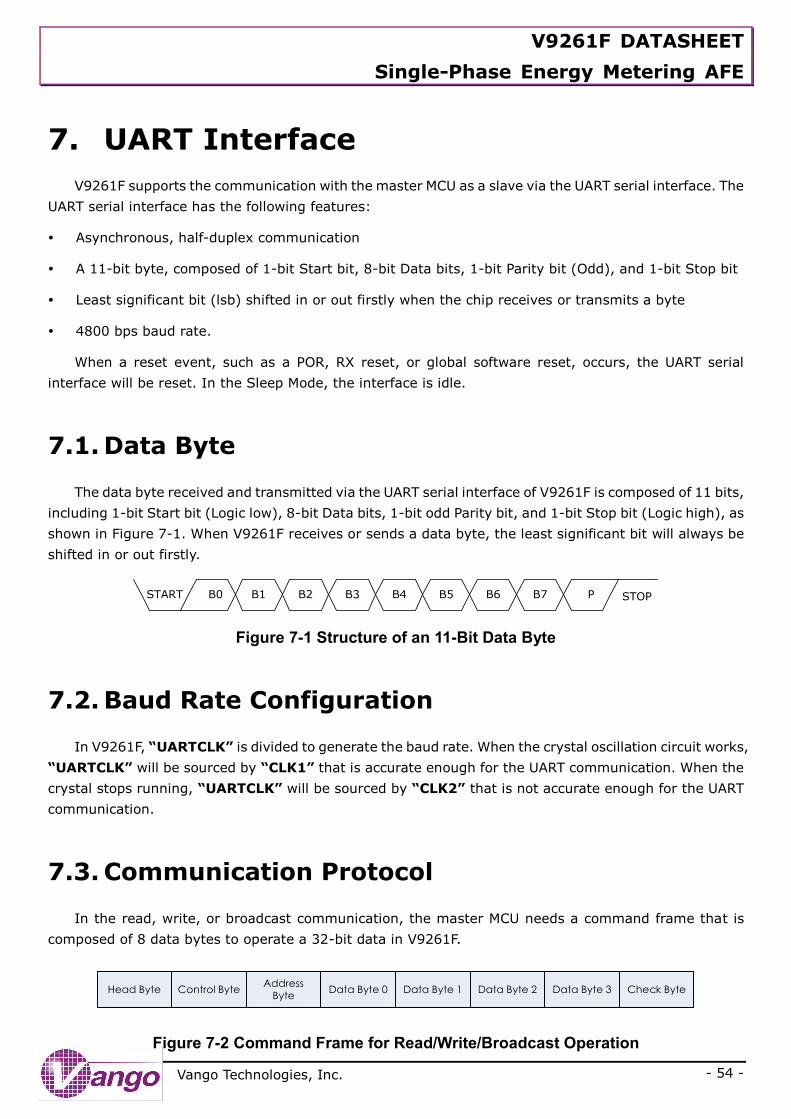
V9261F DATASHEET
Single-Phase Energy Metering AFE
- 54 -
Vango Technologies, Inc.
7. UART Interface
V9261F supports the communication with the master MCU as a slave via the UART serial interface. The
UART serial interface has the following features:
Asynchronous, half-duplex communication
A 11-bit byte, composed of 1-bit Start bit, 8-bit Data bits, 1-bit Parity bit (Odd), and 1-bit Stop bit
Least significant bit (lsb) shifted in or out firstly when the chip receives or transmits a byte
4800 bps baud rate.
When a reset event, such as a POR, RX reset, or global software reset, occurs, the UART serial
interface will be reset. In the Sleep Mode, the interface is idle.
7.1. Data Byte
The data byte received and transmitted via the UART serial interface of V9261F is composed of 11 bits,
including 1-bit Start bit (Logic low), 8-bit Data bits, 1-bit odd Parity bit, and 1-bit Stop bit (Logic high), as
shown in Figure 7-1. When V9261F receives or sends a data byte, the least significant bit will always be
shifted in or out firstly.
START B0 B1 B2 B3 B4 B5 B6 B7 P STOP
Figure 7-1 Structure of an 11-Bit Data Byte
7.2. Baud Rate Configuration
In V9261F, “UARTCLK” is divided to generate the baud rate. When the crystal oscillation circuit works,
“UARTCLK” will be sourced by “CLK1” that is accurate enough for the UART communication. When the
crystal stops running, “UARTCLK” will be sourced by “CLK2” that is not accurate enough for the UART
communication.
7.3. Communication Protocol
In the read, write, or broadcast communication, the master MCU needs a command frame that is
composed of 8 data bytes to operate a 32-bit data in V9261F.
Head Byte Control ByteAddress
ByteData Byte 0 Data Byte 1 Data Byte 2 Data Byte 3 Check Byte
Figure 7-2 Command Frame for Read/Write/Broadcast Operation
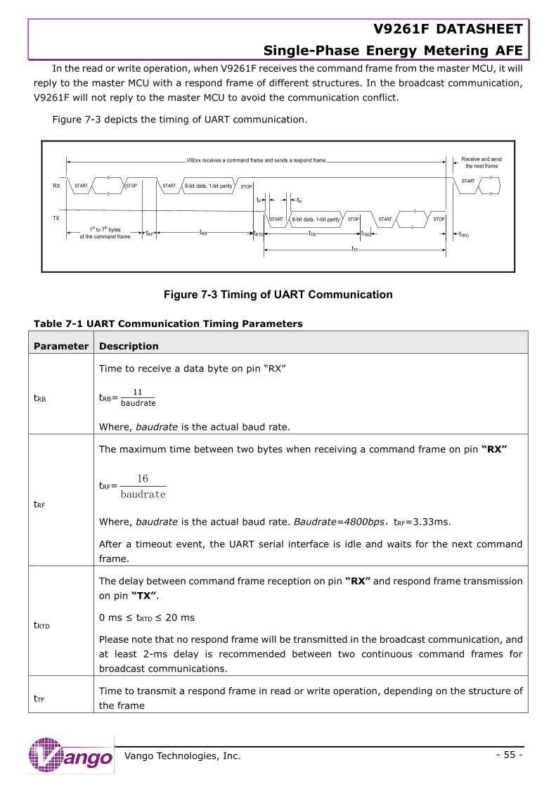
V9261F DATASHEET
Single-Phase Energy Metering AFE
- 55 -
Vango Technologies, Inc.
In the read or write operation, when V9261F receives the command frame from the master MCU, it will
reply to the master MCU with a respond frame of different structures. In the broadcast communication,
V9261F will not reply to the master MCU to avoid the communication conflict.
Figure 7-3 depicts the timing of UART communication.
RX
TX
8-bit data, 1-bit paritySTARTSTART
START STOP
STOP
//
//
START STOP
1st to 7
th bytes
of the command frametRTD
V92xx receives a command frame and sends a respond frame Receive and send
the next frame
tTRD
//
//
//
//
tRB
tTF
8-bit data, 1-bit paritySTART STOP
tTBD
tRtF
tTBtRF
Figure 7-3 Timing of UART Communication
Table 7-1 UART Communication Timing Parameters
Parameter Description
tRB
Time to receive a data byte on pin “RX”
tRB=baudrate
11
Where, baudrate is the actual baud rate.
tRF
The maximum time between two bytes when receiving a command frame on pin “RX”
tRF=baudrate
16
Where, baudrate is the actual baud rate. Baudrate=4800bps,tRF=3.33ms.
After a timeout event, the UART serial interface is idle and waits for the next command
frame.
tRTD
The delay between command frame reception on pin “RX” and respond frame transmission
on pin “TX”.
0 ms ≤ tRTD ≤ 20 ms
Please note that no respond frame will be transmitted in the broadcast communication, and
at least 2-ms delay is recommended between two continuous command frames for
broadcast communications.
tTF Time to transmit a respond frame in read or write operation, depending on the structure of
the frame
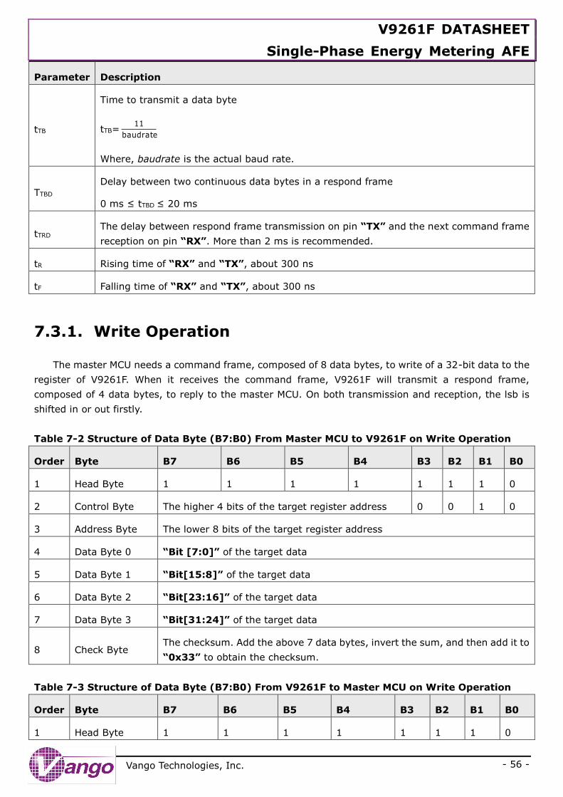
V9261F DATASHEET
Single-Phase Energy Metering AFE
- 56 -
Vango Technologies, Inc.
Parameter Description
tTB
Time to transmit a data byte
tTB=baudrate
11
Where, baudrate is the actual baud rate.
TTBD Delay between two continuous data bytes in a respond frame
0 ms ≤ tTBD ≤ 20 ms
tTRD The delay between respond frame transmission on pin “TX” and the next command frame
reception on pin “RX”. More than 2 ms is recommended.
tR Rising time of “RX” and “TX”, about 300 ns
tF Falling time of “RX” and “TX”, about 300 ns
7.3.1. Write Operation
The master MCU needs a command frame, composed of 8 data bytes, to write of a 32-bit data to the
register of V9261F. When it receives the command frame, V9261F will transmit a respond frame,
composed of 4 data bytes, to reply to the master MCU. On both transmission and reception, the lsb is
shifted in or out firstly.
Table 7-2 Structure of Data Byte (B7:B0) From Master MCU to V9261F on Write Operation
Order Byte B7 B6 B5 B4 B3 B2 B1 B0
1 Head Byte 1 1 1 1 1 1 1 0
2 Control Byte The higher 4 bits of the target register address 0 0 1 0
3 Address Byte The lower 8 bits of the target register address
4 Data Byte 0 “Bit [7:0]” of the target data
5 Data Byte 1 “Bit[15:8]” of the target data
6 Data Byte 2 “Bit[23:16]” of the target data
7 Data Byte 3 “Bit[31:24]” of the target data
8 Check Byte The checksum. Add the above 7 data bytes, invert the sum, and then add it to
“0x33” to obtain the checksum.
Table 7-3 Structure of Data Byte (B7:B0) From V9261F to Master MCU on Write Operation
Order Byte B7 B6 B5 B4 B3 B2 B1 B0
1 Head Byte 1 1 1 1 1 1 1 0
V9261F DATASHEET
Single-Phase Energy Metering AFE
- 57 -
Vango Technologies, Inc.
Order Byte B7 B6 B5 B4 B3 B2 B1 B0
2 Control Byte The higher 4 bits of the target register address 0 0 1 0
3 Address Byte The lower 8 bits of the target register address
4 Check Byte The checksum. Add the above 3 data bytes, invert the sum, and then add it to
“0x33” to obtain the checksum.
7.3.2. Read Operation
The master MCU needs a command frame, composed of 8 data bytes, to read of a 32-bit data of a
register of V9261F. When it receives the command frame, V9261F will transmit a respond frame,
composed of 4×N+4 (1 ≤ N ≤ 255) data bytes, to reply to the master MCU. On both transmission and
reception, the lsb is shifted in or out firstly.
Table 7-4 Structure of Data Byte (B7:B0) From Master MCU to V9261F on Read Operation
Order Byte B7 B6 B5 B4 B3 B2 B1 B0
1 Head Byte 1 1 1 1 1 1 1 0
2 Control Byte The higher 4 bits of the target register address (D1) 0 0 0 1
3 Address Byte The lower 8 bits of the target register address (D1)
4 Data Byte 0
The length (N, in unit of “Word”) of the data to be read from the registers
located at the addresses beginning with the target address (D1) given by the
Control Byte and Address Byte. When Data Byte 0 is ‘0’, it means 1 data word
(4 bytes) is read out.
When the master MCU reads of the target address only, N is ‘1’.
When more than one registers located at continuous addresses beginning with
the target address (D1), N is equal to the number of the address. The
maximum value of N is 255, which means no more than 255 continuous
registers can be read at a time.
5 Data Byte 1
No actual function. 6 Data Byte 2
7 Data Byte 3
8 Check Byte The checksum. Add the above 7 data bytes, invert the sum, and then add it to
“0x33” to obtain the checksum.
Table 7-5 Structure of Data Byte (B7:B0) From V9261F to Master MCU on Read Operation
Order Byte B7 B6 B5 B4 B3 B2 B1 B0
1 Head Byte 1 1 1 1 1 1 1 0
V9261F DATASHEET
Single-Phase Energy Metering AFE
- 58 -
Vango Technologies, Inc.
Order Byte B7 B6 B5 B4 B3 B2 B1 B0
2 Control Byte The higher 4 bits of the target register address (D1) 0 0 0 1
3 Length Byte N, equal to Data Byte 0 sent from master MCU to V9261F on read operation.
When Data Byte 0 is ‘0’, N is equal to ‘1’.
4 Data Byte 10 “Bit[7:0]” of the register located at target address (D1)
5 Data Byte 11 “Bit[15:8]” of the register located at target address (D1)
6 Data Byte 12 “Bit[23:16]” of the register located at target address (D1)
7 Data Byte 13 “Bit[31:24]” of the register located at target address (D1)
8 Data Byte 20 “Bit[7:0]” of the register located at address D2 (D2=D1+1)
9 Data Byte 21 “Bit[15:8]” of the register located at address D2 (D2=D1+1)
… … …
4×N+0 Data Byte N0 “Bit[7:0]” of the register located at address DN (DN=D1+N-1)
4×N+1 Data Byte N1 “Bit[15:8]” of the register located at address DN (DN=D1+N-1)
4×N+2 Data Byte N2 “Bit[23:16]” of the register located at address DN (DN=D1+N-1)
4×N+3 Data Byte N3 “Bit[31:24]” of the register located at address DN (DN=D1+N-1)
4×N+4 Check Byte The checksum. Add the above 4×N+3 data bytes, invert the sum, and then add
it to “0x33” to obtain the checksum.
7.3.3. Broadcast Communication
The master MCU needs a command frame, composed of 8 data bytes, to write a 32-bit data to the
registers of more than one V9261F in the broadcast communication. When receiving a command frame,
V9261F should not transmit a respond frame to reply to the master MCU to avoid the communication error.
On receiving a data frame, the lsb is shifted in or out firstly.
Table 7-6 Structure of Data Byte (B7:B0) From Master MCU to V9261F on Broadcast Operation
Order Byte B7 B6 B5 B4 B3 B2 B1 B0
1 Head Byte 1 1 1 1 1 1 1 0
2 Control Byte The higher 4 bits of the target register address 0 0 0 0
3 Address Byte The lower 8 bits of the target register address
4 Data Byte 0 “Bit [7:0]” of the target data
5 Data Byte 1 “Bit[15:8]” of the target data
6 Data Byte 2 “Bit[23:16]” of the target data

V9261F DATASHEET
Single-Phase Energy Metering AFE
- 59 -
Vango Technologies, Inc.
Order Byte B7 B6 B5 B4 B3 B2 B1 B0
7 Data Byte 3 “Bit[31:24]” of the target data
8 Check Byte The checksum. Add the above 7 data bytes, invert the sum, and then add it to
“0x33” to obtain the checksum.
V9261F DATASHEET
Single-Phase Energy Metering AFE
- 60 -
Vango Technologies, Inc.
8. Interrupt
In V9261F, 7 events can trigger interrupt signals that will set the interrupt flag bits to 1s.
System control register self-checking interrupt: Interrupt output cannot be masked.
Configuration verification interrupt: Interrupt output cannot be masked.
Zero-crossing interrupt: The voltage sign bit is output as the zero-crossing interrupt; interrupt
output can be masked.
Current detection interrupt: Interrupt output cannot be masked in the Current Detection Mode,
and can be masked in other operation modes.
Power down interrupt: Interrupt output can be masked. Please refer to “Power Supply
Monitoring Circuit” for more detailed information.
External crystal failure interrupt: Interrupt output can be masked. Please refer to “Crystal
Oscillation Circuit” for more detailed information.
REF capacitor damage alarm interrupt: Interrupt output can be masked.
The interrupt management circuit keeps on working until it is powered off.
8.1. System Control Register Self-Checking
Interrupt
In V9261F, “bit[8:0]” of the register “SysCtrl” (0x0180) are used for key configuration for the
system operation mode, and “bit[24:16]” are designed as the backup of these bits. Invert the values of
“bit[8:0]”, and write them into “bit[24:16]” sequentially. The internal self-checking circuit compares
the content of these bits all the time. If they are opposite to each other sequentially, it indicates the
configurations are right; otherwise, an interrupt signal will be triggered, the flag bit “SYSERR” (“bit20”
of “SysCtrl”, 0x0180) is set to ‘1’. The flag bit holds the state until the self-checking is corrected.
This interrupt output cannot be masked.
8.2. Configuration Verification Interrupt
To ensure the important configuration of control, configuration and calibration registers are in their
desired states, V9261F introduces the configuration verification measure: Add the content of the register
“CKSUM” (0x0133) and that of the other 24 registers listed in Table 8-1. If the sum is “0xFFFFFFFF”, it
indicates all the configurations are right; otherwise, it indicates some change has occurred to the registers,
an interrupt signal will be triggered, and the flag bit “CHKERR” (bit19 of SysCtrl, 0x0180) will be set to
‘1’. This interrupt output cannot be masked. The configuration verification is executed all the time, and
the sum is calculated once every 5 ms. The flag bit will hold its state until the sum of the content of 25
V9261F DATASHEET
Single-Phase Energy Metering AFE
- 61 -
Vango Technologies, Inc.
registers is “0xFFFFFFFF”.
The register “CKSUM” should be written of the difference between “0xFFFFFFFF” and the sum of
the content of the other 24 registers.
Table 8-1 Registers for Configuration Verification
No. Address Register R/W Default
Value
1 0x0123 ZZDCI To preset the bias for direct current R/W 0
2 0x0124 ZZDCU To preset the bias for direct voltage R/W 0
3 0x0125 BPPARA To set coefficient of the bandpass filter R/W 0
4 0x0126 WBRTI To set gain calibration of the fundamental current RMS R/W 0
5 0x0127 WBPT To set gain calibration of the fundamental active
power R/W 0
6 0x0128 WWBPT To set offset calibration of the fundamental active
power R/W 0
7 0x0129 WBQT To set gain calibration of the fundamental reactive
power R/W 0
8 0x012A WWBQT To set offset calibration of the fundamental reactive
power R/W 0
9 0x012B WBRTU To set gain calibration of the fundamental voltage RMS R/W 0
10 0x012C WARTI To set gain calibration of the total current RMS R/W 0
11 0x012D WARTM To set a value to gain calibrate the RMS value of
various signal in Measurement Channel R/W 0
12 0x012E WAPT To set gain calibration of the total active power R/W 0
13 0x012F WWAPT To set offset calibration of the total active power R/W 0
14 0x0130 WAQT To set gain calibration of the total reactive power R/W 0
15 0x0131 WWAQT To set offset calibration of the total reactive power R/W 0
16 0x0132 WARTU To set gain calibration of the total voltage RMS R/W 0
17 0x0134 IDETTH To set the threshold for current detection R/W 0
18 0x0181 EGYTH To set a threshold for energy-to-pulse conversion R/W 0
19 0x0182 CTH To set a threshold for no-load detection R/W 0
20 0x0183 MTPARA0 Metering control register 0 R/W 0
21 0x0184 MTPARA1 Metering control register 1 R/W 0x400000
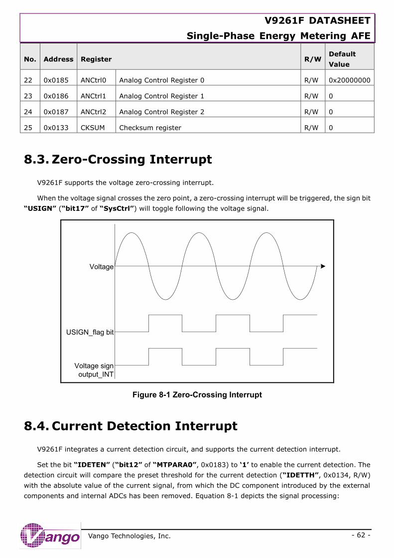
V9261F DATASHEET
Single-Phase Energy Metering AFE
- 62 -
Vango Technologies, Inc.
No. Address Register R/W Default
Value
22 0x0185 ANCtrl0 Analog Control Register 0 R/W 0x20000000
23 0x0186 ANCtrl1 Analog Control Register 1 R/W 0
24 0x0187 ANCtrl2 Analog Control Register 2 R/W 0
25 0x0133 CKSUM Checksum register R/W 0
8.3. Zero-Crossing Interrupt
V9261F supports the voltage zero-crossing interrupt.
When the voltage signal crosses the zero point, a zero-crossing interrupt will be triggered, the sign bit
“USIGN” (“bit17” of “SysCtrl”) will toggle following the voltage signal.
Voltage sign
output_INT
USIGN_flag bit
Voltage
Figure 8-1 Zero-Crossing Interrupt
8.4. Current Detection Interrupt
V9261F integrates a current detection circuit, and supports the current detection interrupt.
Set the bit “IDETEN” (“bit12” of “MTPARA0”, 0x0183) to ‘1’ to enable the current detection. The
detection circuit will compare the preset threshold for the current detection (“IDETTH”, 0x0134, R/W)
with the absolute value of the current signal, from which the DC component introduced by the external
components and internal ADCs has been removed. Equation 8-1 depicts the signal processing:
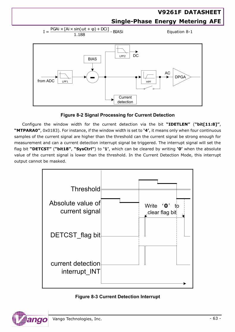
V9261F DATASHEET
Single-Phase Energy Metering AFE
- 63 -
Vango Technologies, Inc.
BIASi-188.1
]DCi+)φ+tωsin(×Ai[×PGAi=I Equation 8-1
-
BIAS
from ADC
Current
detection
AC
DC
DPGALPF1
LPF2
HPF
Figure 8-2 Signal Processing for Current Detection
Configure the window width for the current detection via the bit “IDETLEN” (“bit[11:8]”,
“MTPARA0”, 0x0183). For instance, if the window width is set to ‘4’, it means only when four continuous
samples of the current signal are higher than the threshold can the current signal be strong enough for
measurement and can a current detection interrupt signal be triggered. The interrupt signal will set the
flag bit “DETCST” (“bit18”, “SysCtrl”) to ‘1’, which can be cleared by writing ‘0’ when the absolute
value of the current signal is lower than the threshold. In the Current Detection Mode, this interrupt
output cannot be masked.
Absolute value of
current signal
Threshold
DETCST_flag bit
current detection
interrupt_INT
Write ‘0’ to
clear flag bit
Figure 8-3 Current Detection Interrupt
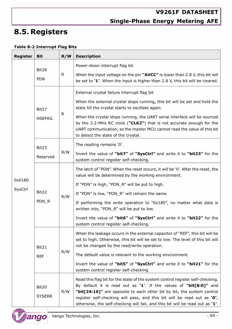
V9261F DATASHEET
Single-Phase Energy Metering AFE
- 64 -
Vango Technologies, Inc.
8.5. Registers
Table 8-2 Interrupt Flag Bits
Register Bit R/W Description
0x0180
SysCtrl
Bit28
PDN R
Power-down interrupt flag bit
When the input voltage on the pin “AVCC” is lower than 2.8 V, this bit will
be set to ‘1’. When the input is higher than 2.8 V, this bit will be cleared.
Bit27
HSEFAIL R
External crystal failure interrupt flag bit
When the external crystal stops running, this bit will be set and hold the
state till the crystal starts to oscillate again.
When the crystal stops running, the UART serial interface will be sourced
by the 3.2-MHz RC clock (“CLK2”) that is not accurate enough for the
UART communication, so the master MCU cannot read the value of this bit
to detect the state of the crystal.
Bit23
Reserved R/W
The reading remains ‘0’.
Invert the value of “bit7” of “SysCtrl” and write it to “bit23” for the
system control register self-checking.
Bit22
PDN_R R/W
The latch of “PDN”. When the reset occurs, it will be ‘0’. After the reset, the
value will be determined by the working environment.
If “PDN” is high, “PDN_R” will be put to high.
If “PDN” is low, “PDN_R” will remain the same.
If performing the write operation to “0x180”, no matter what data is
written into, “PDN_R” will be put to low.
Invert the value of “bit6” of “SysCtrl” and write it to “bit22” for the
system control register self-checking.
Bit21
REF R/W
When the leakage occurs in the external capacitor of “REF”, this bit will be
set to high. Otherwise, this bit will be set to low. The level of this bit will
not be changed by the read/write operation.
The default value is relevant to the working environment.
Invert the value of “bit5” of “SysCtrl” and write it to “bit21” for the
system control register self-checking.
Bit20
SYSERR R/W
Read this flag bit for the state of the system control register self-checking.
By default it is read out as ‘1’. If the values of “bit[8:0]” and
“bit[24:16]” are opposite to each other bit by bit, the system control
register self-checking will pass, and this bit will be read out as ‘0’;
otherwise, the self-checking will fail, and this bit will be read out as ‘1’.
V9261F DATASHEET
Single-Phase Energy Metering AFE
- 65 -
Vango Technologies, Inc.
Register Bit R/W Description
Only writing the exact opposite values of “bit[8:0]” to “bit[24:16]” can
clear this bit.
Invert the value of “bit4” of “SysCtrl” and write it to “bit20” for the
system control register self-checking.
Bit19
CHKERR R/W
Read this bit for the state of configuration verification
Add the content of the registers for calibration, metering control registers
and analog control registers to the content of the checksum register to
ensure that all the important configurations are in their desired states. If
the sum is “0xFFFFFFFF”, the verification will pass, and this bit will be
read out as ‘0’; otherwise, the verification will fail, and this bit will be read
out as ‘1’.
Invert the value of “bit3” of “SysCtrl” and write it to “bit19” for the
system control register self-checking.
Bit18
DETCST R/W
Current detection interrupt flag bit
When some continuous samples of the current signal are higher than the
preset threshold, this bit will be set to ‘1’ to indicate that a current signal
is caught. This bit can be cleared only by writing ‘0’ to it when the current
samples are lower than the threshold.
Invert the value of “bit2” of “SysCtrl” and write it to “bit18” for the
system control register self-checking.
Bit17
USIGN R/W
Voltage sign bit
1: Negative
0: Positive
Read this bit to detect the sign of the voltage. This bit toggles following
the sign of the voltage.
Invert the value of “bit1” of “SysCtrl” and write it to “bit17” for the
system control register self-checking.
V9261F DATASHEET
Single-Phase Energy Metering AFE
- 66 -
Vango Technologies, Inc.
9. Registers
9.1. Analog Control Registers
All analog control registers of V9261F, located at addresses “0x0185” ~ “0x0187”, will be reset to
their default values when a Power-On Reset (POR), RX reset, or global software reset occurs. All the
default values in the following tables are in the format of hexadecimal. All analog control registers are
readable and writable. Their configurations must be verified all the time.
Table 9-1 Analog Control Register 0 (ANCtrl0, 0x0185)
0x0185, R/W, Analog Control Register 0, ANCtrl0
Bit Default Function Description
Bit[31:30] Reserved 0 These bits must be set to “0b11” for proper operation.
Bit29 PDRCCLK N/A
Clear this bit to enable the 3.2-MHz RC Clock. It is mandatory
to enable the BandGap circuit and biasing circuit firstly. The
value of the bit is uncertain when the system is reset.
In the Sleep Mode, this bit is set to ‘1’ automatically. In the
Current Detection Mode, this bit is cleared automatically.
In the Metering Mode, when the chip operates with full
functions, it is recommended to disable this circuit (Set the bit
to ‘1’).
Bit28 BIASPDN 0
Set this bit to ‘1’ to enable the biasing circuit to provide the
global biasing current for ADCs and the 3.2-MHz RC oscillator.
Therefore, in the Metering Mode, when the chip operates with
full functions, this bit must be set to ‘1’ before enabling ADCs
and the 3.2-MHz RC oscillator. By default the biasing circuit is
disabled.
In the Sleep Mode, this bit is cleared automatically. In the
Current Detection Mode, this bit is set to ‘1’ automatically.
Bit27 BGPPDN 0
Set this bit to ‘1’ to enable the BandGap circuit to provide
ADCs and the 3.2-MHz RC oscillator with the reference voltage
and biasing voltage. Therefore, in the Metering Mode, when
the chip operates with full functions, this bit must be set to ‘1’
before enabling ADCs and the 3.2-MHz RC oscillator. By default
the BandGap circuit is disabled.
In the Sleep Mode, this bit is cleared automatically. In the
Current Detection Mode, this bit is set to ‘1’ automatically.
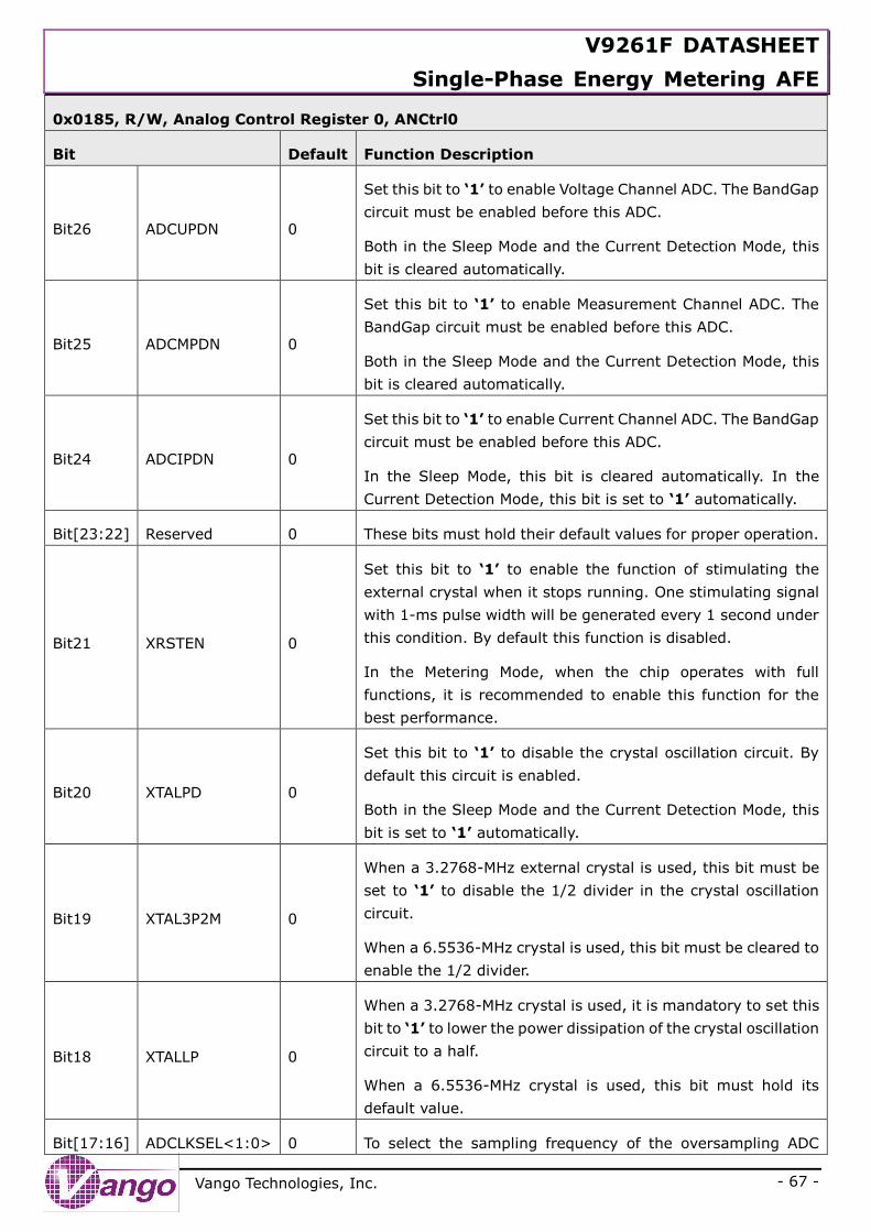
V9261F DATASHEET
Single-Phase Energy Metering AFE
- 67 -
Vango Technologies, Inc.
0x0185, R/W, Analog Control Register 0, ANCtrl0
Bit Default Function Description
Bit26 ADCUPDN 0
Set this bit to ‘1’ to enable Voltage Channel ADC. The BandGap
circuit must be enabled before this ADC.
Both in the Sleep Mode and the Current Detection Mode, this
bit is cleared automatically.
Bit25 ADCMPDN 0
Set this bit to ‘1’ to enable Measurement Channel ADC. The
BandGap circuit must be enabled before this ADC.
Both in the Sleep Mode and the Current Detection Mode, this
bit is cleared automatically.
Bit24 ADCIPDN 0
Set this bit to ‘1’ to enable Current Channel ADC. The BandGap
circuit must be enabled before this ADC.
In the Sleep Mode, this bit is cleared automatically. In the
Current Detection Mode, this bit is set to ‘1’ automatically.
Bit[23:22] Reserved 0 These bits must hold their default values for proper operation.
Bit21 XRSTEN 0
Set this bit to ‘1’ to enable the function of stimulating the
external crystal when it stops running. One stimulating signal
with 1-ms pulse width will be generated every 1 second under
this condition. By default this function is disabled.
In the Metering Mode, when the chip operates with full
functions, it is recommended to enable this function for the
best performance.
Bit20 XTALPD 0
Set this bit to ‘1’ to disable the crystal oscillation circuit. By
default this circuit is enabled.
Both in the Sleep Mode and the Current Detection Mode, this
bit is set to ‘1’ automatically.
Bit19 XTAL3P2M 0
When a 3.2768-MHz external crystal is used, this bit must be
set to ‘1’ to disable the 1/2 divider in the crystal oscillation
circuit.
When a 6.5536-MHz crystal is used, this bit must be cleared to
enable the 1/2 divider.
Bit18 XTALLP 0
When a 3.2768-MHz crystal is used, it is mandatory to set this
bit to ‘1’ to lower the power dissipation of the crystal oscillation
circuit to a half.
When a 6.5536-MHz crystal is used, this bit must hold its
default value.
Bit[17:16] ADCLKSEL<1:0> 0 To select the sampling frequency of the oversampling ADC
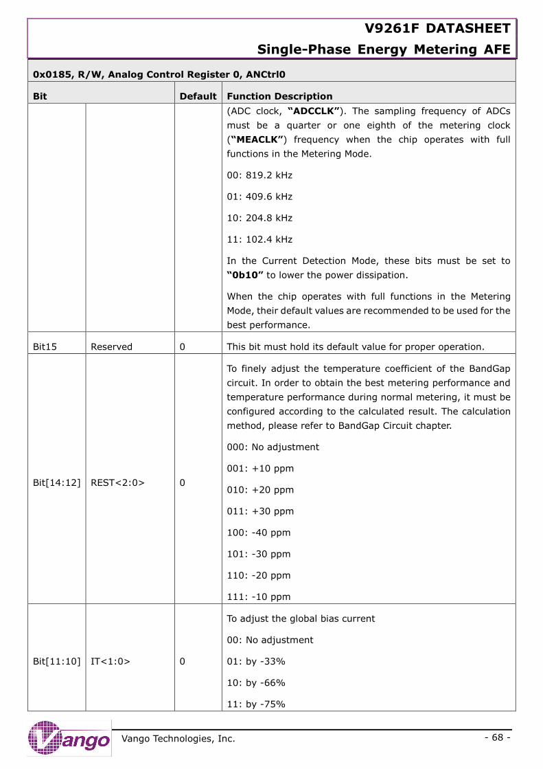
V9261F DATASHEET
Single-Phase Energy Metering AFE
- 68 -
Vango Technologies, Inc.
0x0185, R/W, Analog Control Register 0, ANCtrl0
Bit Default Function Description
(ADC clock, “ADCCLK”). The sampling frequency of ADCs
must be a quarter or one eighth of the metering clock
(“MEACLK”) frequency when the chip operates with full
functions in the Metering Mode.
00: 819.2 kHz
01: 409.6 kHz
10: 204.8 kHz
11: 102.4 kHz
In the Current Detection Mode, these bits must be set to
“0b10” to lower the power dissipation.
When the chip operates with full functions in the Metering
Mode, their default values are recommended to be used for the
best performance.
Bit15 Reserved 0 This bit must hold its default value for proper operation.
Bit[14:12] REST<2:0> 0
To finely adjust the temperature coefficient of the BandGap
circuit. In order to obtain the best metering performance and
temperature performance during normal metering, it must be
configured according to the calculated result. The calculation
method, please refer to BandGap Circuit chapter.
000: No adjustment
001: +10 ppm
010: +20 ppm
011: +30 ppm
100: -40 ppm
101: -30 ppm
110: -20 ppm
111: -10 ppm
Bit[11:10] IT<1:0> 0
To adjust the global bias current
00: No adjustment
01: by -33%
10: by -66%
11: by -75%
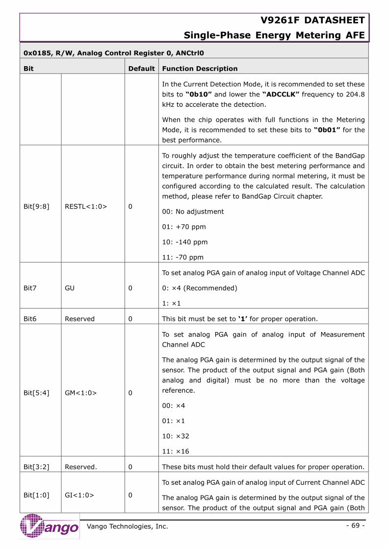
V9261F DATASHEET
Single-Phase Energy Metering AFE
- 69 -
Vango Technologies, Inc.
0x0185, R/W, Analog Control Register 0, ANCtrl0
Bit Default Function Description
In the Current Detection Mode, it is recommended to set these
bits to “0b10” and lower the “ADCCLK” frequency to 204.8
kHz to accelerate the detection.
When the chip operates with full functions in the Metering
Mode, it is recommended to set these bits to “0b01” for the
best performance.
Bit[9:8] RESTL<1:0> 0
To roughly adjust the temperature coefficient of the BandGap
circuit. In order to obtain the best metering performance and
temperature performance during normal metering, it must be
configured according to the calculated result. The calculation
method, please refer to BandGap Circuit chapter.
00: No adjustment
01: +70 ppm
10: -140 ppm
11: -70 ppm
Bit7 GU 0
To set analog PGA gain of analog input of Voltage Channel ADC
0: ×4 (Recommended)
1: ×1
Bit6 Reserved 0 This bit must be set to ‘1’ for proper operation.
Bit[5:4] GM<1:0> 0
To set analog PGA gain of analog input of Measurement
Channel ADC
The analog PGA gain is determined by the output signal of the
sensor. The product of the output signal and PGA gain (Both
analog and digital) must be no more than the voltage
reference.
00: ×4
01: ×1
10: ×32
11: ×16
Bit[3:2] Reserved. 0 These bits must hold their default values for proper operation.
Bit[1:0] GI<1:0> 0
To set analog PGA gain of analog input of Current Channel ADC
The analog PGA gain is determined by the output signal of the
sensor. The product of the output signal and PGA gain (Both
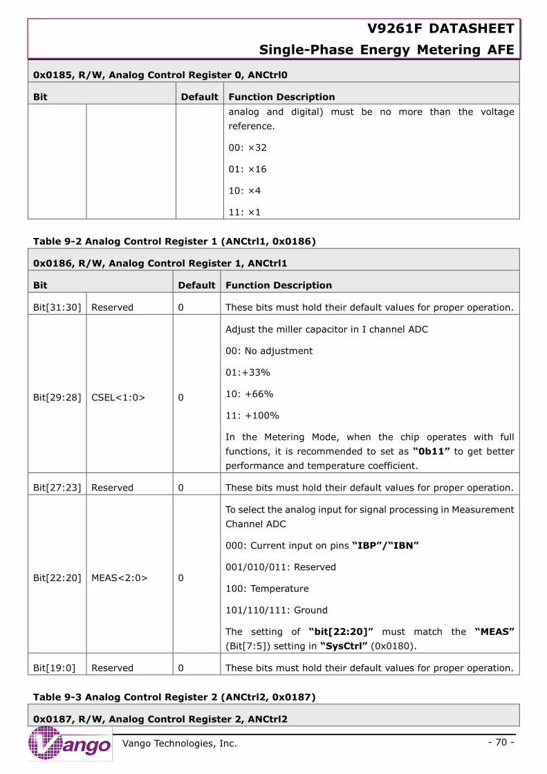
V9261F DATASHEET
Single-Phase Energy Metering AFE
- 70 -
Vango Technologies, Inc.
0x0185, R/W, Analog Control Register 0, ANCtrl0
Bit Default Function Description
analog and digital) must be no more than the voltage
reference.
00: ×32
01: ×16
10: ×4
11: ×1
Table 9-2 Analog Control Register 1 (ANCtrl1, 0x0186)
0x0186, R/W, Analog Control Register 1, ANCtrl1
Bit Default Function Description
Bit[31:30] Reserved 0 These bits must hold their default values for proper operation.
Bit[29:28] CSEL<1:0> 0
Adjust the miller capacitor in I channel ADC
00: No adjustment
01:+33%
10: +66%
11: +100%
In the Metering Mode, when the chip operates with full
functions, it is recommended to set as “0b11” to get better
performance and temperature coefficient.
Bit[27:23] Reserved 0 These bits must hold their default values for proper operation.
Bit[22:20] MEAS<2:0> 0
To select the analog input for signal processing in Measurement
Channel ADC
000: Current input on pins “IBP”/“IBN”
001/010/011: Reserved
100: Temperature
101/110/111: Ground
The setting of “bit[22:20]” must match the “MEAS”
(Bit[7:5]) setting in “SysCtrl” (0x0180).
Bit[19:0] Reserved 0 These bits must hold their default values for proper operation.
Table 9-3 Analog Control Register 2 (ANCtrl2, 0x0187)
0x0187, R/W, Analog Control Register 2, ANCtrl2
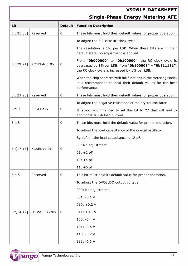
V9261F DATASHEET
Single-Phase Energy Metering AFE
- 71 -
Vango Technologies, Inc.
Bit Default Function Description
Bit[31:30] Reserved 0 These bits must hold their default values for proper operation.
Bit[29:24] RCTRIM<5:0> 0
To adjust the 3.2-MHz RC clock cycle
The resolution is 1% per LSB. When these bits are in their
default state, no adjustment is applied.
From “0b000000” to “0b100000”, the RC clock cycle is
decreased by 1% per LSB; from “0b100001” ~ “0b111111”,
the RC clock cycle is increased by 1% per LSB.
When the chip operates with full functions in the Metering Mode,
it is recommended to hold their default values for the best
performance.
Bit[23:20] Reserved 0 These bits must hold their default values for proper operation.
Bit19 XRSEL<1> 0
To adjust the negative resistance of the crystal oscillator
It is not recommended to set this bit to ‘1’ that will lead to
additional 18-μA load current.
Bit18 - 0 These bits must hold the default value for proper operation.
Bit[17:16] XCSEL<1:0> 0
To adjust the load capacitance of the crystal oscillator
By default the load capacitance is 12 pF.
00: No adjustment
01: +2 pF
10: +4 pF
11: +6 pF
Bit15 Reserved 0 This bit must hold its default value for proper operation.
Bit[14:12] LDOVSEL<2:0> 0
To adjust the DVCCLDO output voltage
000: No adjustment
001: -0.1 V
010: +0.2 V
011: +0.1 V
100: -0.4 V
101: -0.5 V
110: -0.2 V
111: -0.3 V
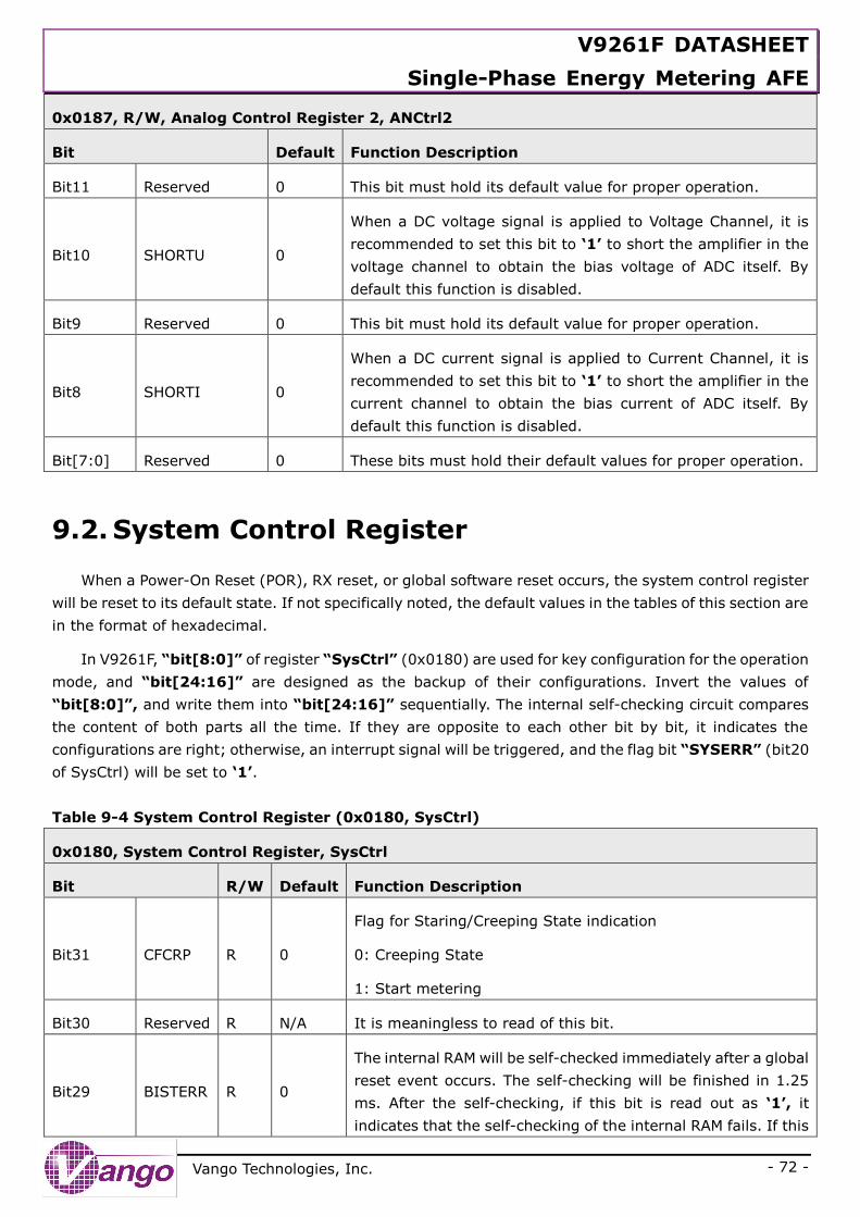
V9261F DATASHEET
Single-Phase Energy Metering AFE
- 72 -
Vango Technologies, Inc.
0x0187, R/W, Analog Control Register 2, ANCtrl2
Bit Default Function Description
Bit11 Reserved 0 This bit must hold its default value for proper operation.
Bit10 SHORTU 0
When a DC voltage signal is applied to Voltage Channel, it is
recommended to set this bit to ‘1’ to short the amplifier in the
voltage channel to obtain the bias voltage of ADC itself. By
default this function is disabled.
Bit9 Reserved 0 This bit must hold its default value for proper operation.
Bit8 SHORTI 0
When a DC current signal is applied to Current Channel, it is
recommended to set this bit to ‘1’ to short the amplifier in the
current channel to obtain the bias current of ADC itself. By
default this function is disabled.
Bit[7:0] Reserved 0 These bits must hold their default values for proper operation.
9.2. System Control Register
When a Power-On Reset (POR), RX reset, or global software reset occurs, the system control register
will be reset to its default state. If not specifically noted, the default values in the tables of this section are
in the format of hexadecimal.
In V9261F, “bit[8:0]” of register “SysCtrl” (0x0180) are used for key configuration for the operation
mode, and “bit[24:16]” are designed as the backup of their configurations. Invert the values of
“bit[8:0]”, and write them into “bit[24:16]” sequentially. The internal self-checking circuit compares
the content of both parts all the time. If they are opposite to each other bit by bit, it indicates the
configurations are right; otherwise, an interrupt signal will be triggered, and the flag bit “SYSERR” (bit20
of SysCtrl) will be set to ‘1’.
Table 9-4 System Control Register (0x0180, SysCtrl)
0x0180, System Control Register, SysCtrl
Bit R/W Default Function Description
Bit31 CFCRP R 0
Flag for Staring/Creeping State indication
0: Creeping State
1: Start metering
Bit30 Reserved R N/A It is meaningless to read of this bit.
Bit29 BISTERR R 0
The internal RAM will be self-checked immediately after a global
reset event occurs. The self-checking will be finished in 1.25
ms. After the self-checking, if this bit is read out as ‘1’, it
indicates that the self-checking of the internal RAM fails. If this
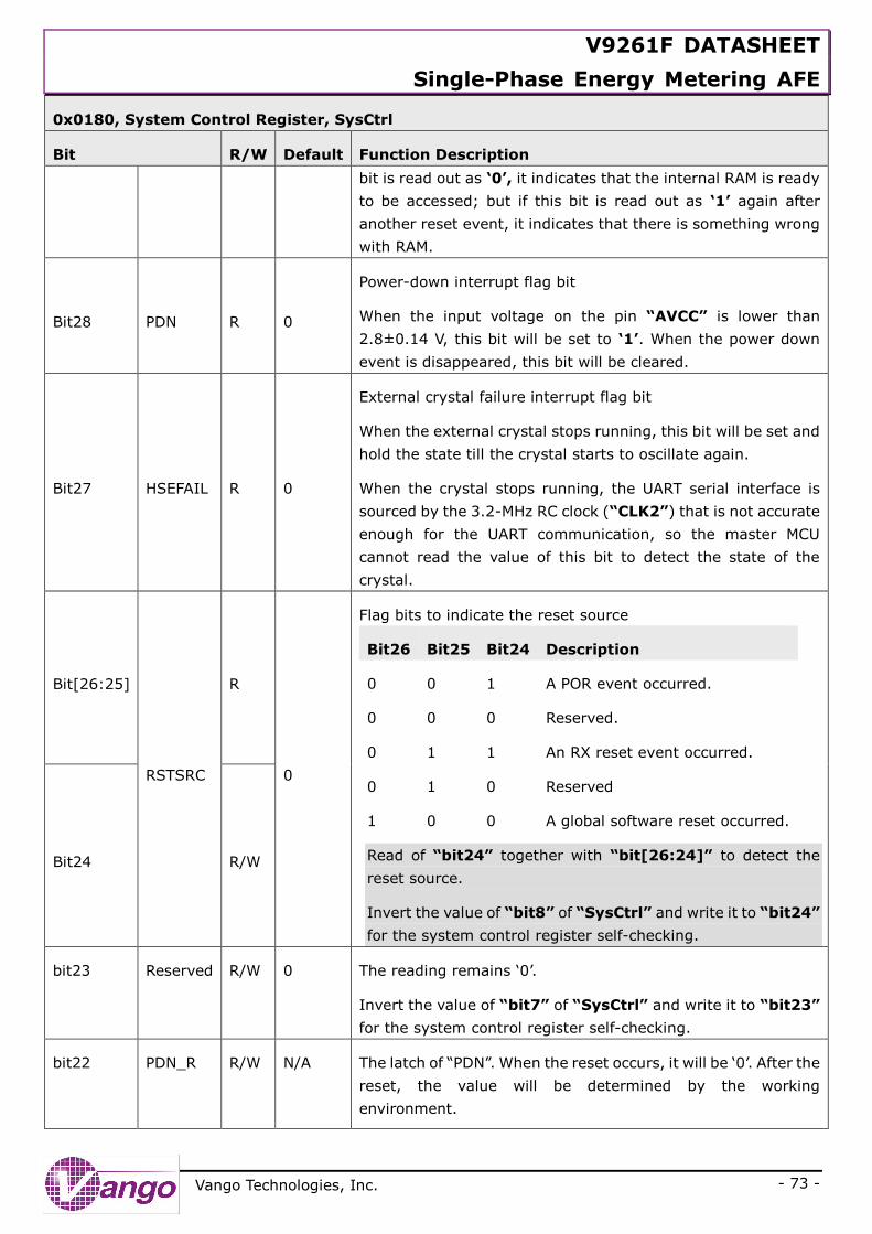
V9261F DATASHEET
Single-Phase Energy Metering AFE
- 73 -
Vango Technologies, Inc.
0x0180, System Control Register, SysCtrl
Bit R/W Default Function Description
bit is read out as ‘0’, it indicates that the internal RAM is ready
to be accessed; but if this bit is read out as ‘1’ again after
another reset event, it indicates that there is something wrong
with RAM.
Bit28 PDN R 0
Power-down interrupt flag bit
When the input voltage on the pin “AVCC” is lower than
2.8±0.14 V, this bit will be set to ‘1’. When the power down
event is disappeared, this bit will be cleared.
Bit27 HSEFAIL R 0
External crystal failure interrupt flag bit
When the external crystal stops running, this bit will be set and
hold the state till the crystal starts to oscillate again.
When the crystal stops running, the UART serial interface is
sourced by the 3.2-MHz RC clock (“CLK2”) that is not accurate
enough for the UART communication, so the master MCU
cannot read the value of this bit to detect the state of the
crystal.
Bit[26:25]
RSTSRC
R
0
Flag bits to indicate the reset source
Bit26 Bit25 Bit24 Description
0 0 1 A POR event occurred.
0 0 0 Reserved.
0 1 1 An RX reset event occurred.
0 1 0 Reserved
1 0 0 A global software reset occurred.
Read of “bit24” together with “bit[26:24]” to detect the
reset source.
Invert the value of “bit8” of “SysCtrl” and write it to “bit24”
for the system control register self-checking.
Bit24 R/W
bit23 Reserved R/W 0 The reading remains ‘0’.
Invert the value of “bit7” of “SysCtrl” and write it to “bit23”
for the system control register self-checking.
bit22 PDN_R R/W N/A The latch of “PDN”. When the reset occurs, it will be ‘0’. After the
reset, the value will be determined by the working
environment.
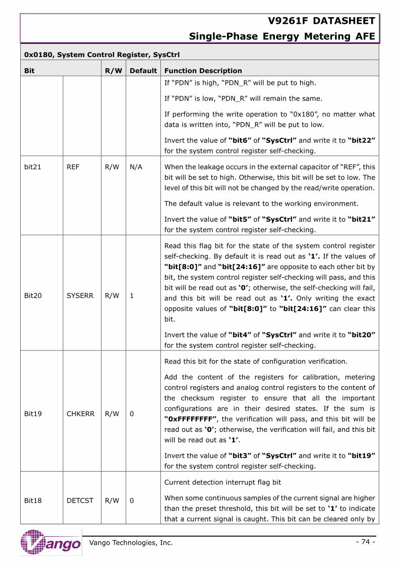
V9261F DATASHEET
Single-Phase Energy Metering AFE
- 74 -
Vango Technologies, Inc.
0x0180, System Control Register, SysCtrl
Bit R/W Default Function Description
If “PDN” is high, “PDN_R” will be put to high.
If “PDN” is low, “PDN_R” will remain the same.
If performing the write operation to “0x180”, no matter what
data is written into, “PDN_R” will be put to low.
Invert the value of “bit6” of “SysCtrl” and write it to “bit22”
for the system control register self-checking.
bit21 REF R/W N/A When the leakage occurs in the external capacitor of “REF”, this
bit will be set to high. Otherwise, this bit will be set to low. The
level of this bit will not be changed by the read/write operation.
The default value is relevant to the working environment.
Invert the value of “bit5” of “SysCtrl” and write it to “bit21”
for the system control register self-checking.
Bit20 SYSERR R/W 1
Read this flag bit for the state of the system control register
self-checking. By default it is read out as ‘1’. If the values of
“bit[8:0]” and “bit[24:16]” are opposite to each other bit by
bit, the system control register self-checking will pass, and this
bit will be read out as ‘0’; otherwise, the self-checking will fail,
and this bit will be read out as ‘1’. Only writing the exact
opposite values of “bit[8:0]” to “bit[24:16]” can clear this
bit.
Invert the value of “bit4” of “SysCtrl” and write it to “bit20”
for the system control register self-checking.
Bit19 CHKERR R/W 0
Read this bit for the state of configuration verification.
Add the content of the registers for calibration, metering
control registers and analog control registers to the content of
the checksum register to ensure that all the important
configurations are in their desired states. If the sum is
“0xFFFFFFFF”, the verification will pass, and this bit will be
read out as ‘0’; otherwise, the verification will fail, and this bit
will be read out as ‘1’.
Invert the value of “bit3” of “SysCtrl” and write it to “bit19”
for the system control register self-checking.
Bit18 DETCST R/W 0
Current detection interrupt flag bit
When some continuous samples of the current signal are higher
than the preset threshold, this bit will be set to ‘1’ to indicate
that a current signal is caught. This bit can be cleared only by
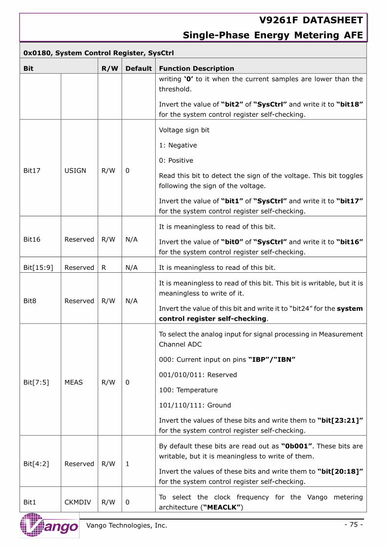
V9261F DATASHEET
Single-Phase Energy Metering AFE
- 75 -
Vango Technologies, Inc.
0x0180, System Control Register, SysCtrl
Bit R/W Default Function Description
writing ‘0’ to it when the current samples are lower than the
threshold.
Invert the value of “bit2” of “SysCtrl” and write it to “bit18”
for the system control register self-checking.
Bit17 USIGN R/W 0
Voltage sign bit
1: Negative
0: Positive
Read this bit to detect the sign of the voltage. This bit toggles
following the sign of the voltage.
Invert the value of “bit1” of “SysCtrl” and write it to “bit17”
for the system control register self-checking.
Bit16 Reserved R/W N/A
It is meaningless to read of this bit.
Invert the value of “bit0” of “SysCtrl” and write it to “bit16”
for the system control register self-checking.
Bit[15:9] Reserved R N/A It is meaningless to read of this bit.
Bit8 Reserved R/W N/A
It is meaningless to read of this bit. This bit is writable, but it is
meaningless to write of it.
Invert the value of this bit and write it to “bit24” for the system
control register self-checking.
Bit[7:5] MEAS R/W 0
To select the analog input for signal processing in Measurement
Channel ADC
000: Current input on pins “IBP”/“IBN”
001/010/011: Reserved
100: Temperature
101/110/111: Ground
Invert the values of these bits and write them to “bit[23:21]”
for the system control register self-checking.
Bit[4:2] Reserved R/W 1
By default these bits are read out as “0b001”. These bits are
writable, but it is meaningless to write of them.
Invert the values of these bits and write them to “bit[20:18]”
for the system control register self-checking.
Bit1 CKMDIV R/W 0 To select the clock frequency for the Vango metering
architecture (“MEACLK”)
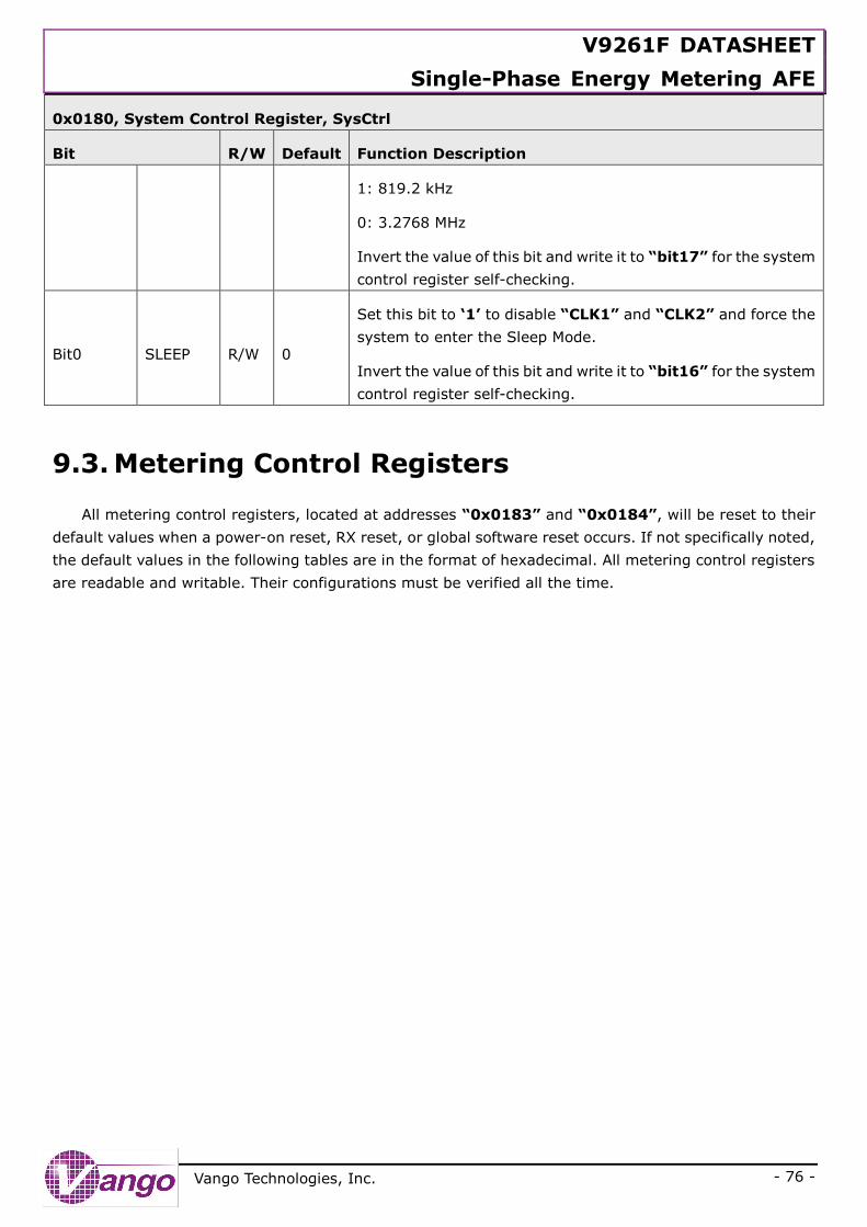
V9261F DATASHEET
Single-Phase Energy Metering AFE
- 76 -
Vango Technologies, Inc.
0x0180, System Control Register, SysCtrl
Bit R/W Default Function Description
1: 819.2 kHz
0: 3.2768 MHz
Invert the value of this bit and write it to “bit17” for the system
control register self-checking.
Bit0 SLEEP R/W 0
Set this bit to ‘1’ to disable “CLK1” and “CLK2” and force the
system to enter the Sleep Mode.
Invert the value of this bit and write it to “bit16” for the system
control register self-checking.
9.3. Metering Control Registers
All metering control registers, located at addresses “0x0183” and “0x0184”, will be reset to their
default values when a power-on reset, RX reset, or global software reset occurs. If not specifically noted,
the default values in the following tables are in the format of hexadecimal. All metering control registers
are readable and writable. Their configurations must be verified all the time.
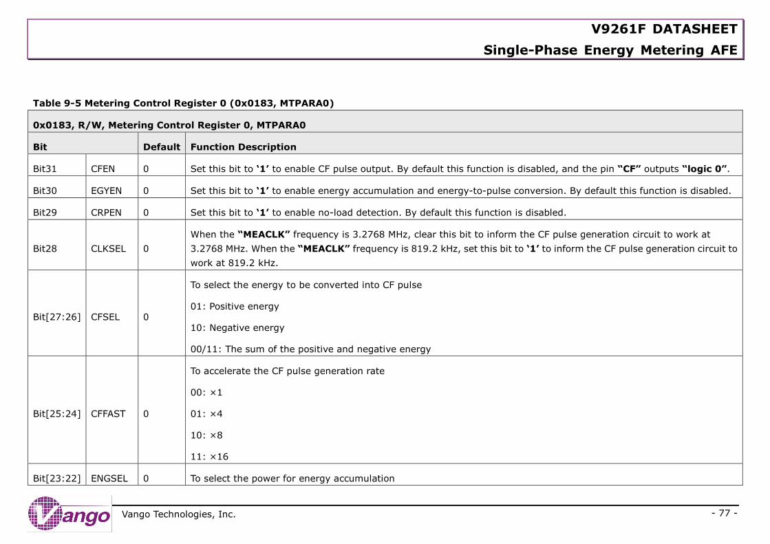
V9261F DATASHEET
Single-Phase Energy Metering AFE
- 77 -
Vango Technologies, Inc.
Table 9-5 Metering Control Register 0 (0x0183, MTPARA0)
0x0183, R/W, Metering Control Register 0, MTPARA0
Bit Default Function Description
Bit31 CFEN 0 Set this bit to ‘1’ to enable CF pulse output. By default this function is disabled, and the pin “CF” outputs “logic 0”.
Bit30 EGYEN 0 Set this bit to ‘1’ to enable energy accumulation and energy-to-pulse conversion. By default this function is disabled.
Bit29 CRPEN 0 Set this bit to ‘1’ to enable no-load detection. By default this function is disabled.
Bit28 CLKSEL 0
When the “MEACLK” frequency is 3.2768 MHz, clear this bit to inform the CF pulse generation circuit to work at
3.2768 MHz. When the “MEACLK” frequency is 819.2 kHz, set this bit to ‘1’ to inform the CF pulse generation circuit to
work at 819.2 kHz.
Bit[27:26] CFSEL 0
To select the energy to be converted into CF pulse
01: Positive energy
10: Negative energy
00/11: The sum of the positive and negative energy
Bit[25:24] CFFAST 0
To accelerate the CF pulse generation rate
00: ×1
01: ×4
10: ×8
11: ×16
Bit[23:22] ENGSEL 0 To select the power for energy accumulation
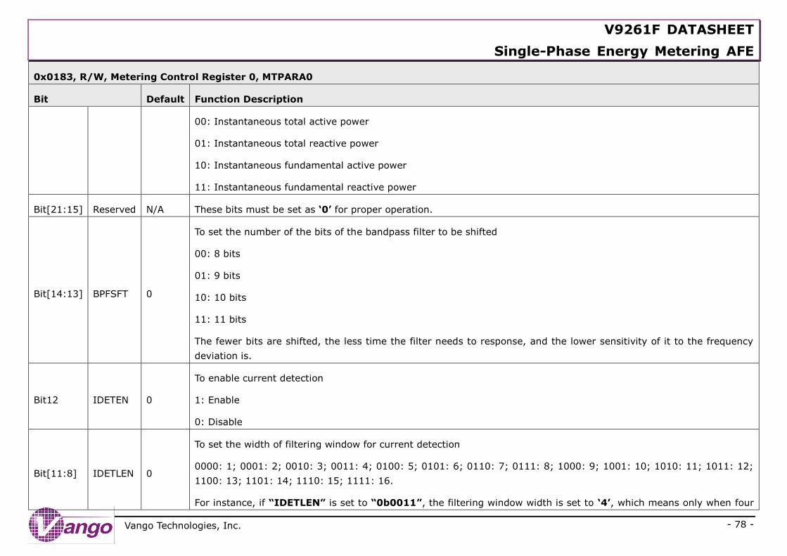
V9261F DATASHEET
Single-Phase Energy Metering AFE
- 78 -
Vango Technologies, Inc.
0x0183, R/W, Metering Control Register 0, MTPARA0
Bit Default Function Description
00: Instantaneous total active power
01: Instantaneous total reactive power
10: Instantaneous fundamental active power
11: Instantaneous fundamental reactive power
Bit[21:15] Reserved N/A These bits must be set as ‘0’ for proper operation.
Bit[14:13] BPFSFT 0
To set the number of the bits of the bandpass filter to be shifted
00: 8 bits
01: 9 bits
10: 10 bits
11: 11 bits
The fewer bits are shifted, the less time the filter needs to response, and the lower sensitivity of it to the frequency
deviation is.
Bit12 IDETEN 0
To enable current detection
1: Enable
0: Disable
Bit[11:8] IDETLEN 0
To set the width of filtering window for current detection
0000: 1; 0001: 2; 0010: 3; 0011: 4; 0100: 5; 0101: 6; 0110: 7; 0111: 8; 1000: 9; 1001: 10; 1010: 11; 1011: 12;
1100: 13; 1101: 14; 1110: 15; 1111: 16.
For instance, if “IDETLEN” is set to “0b0011”, the filtering window width is set to ‘4’, which means only when four
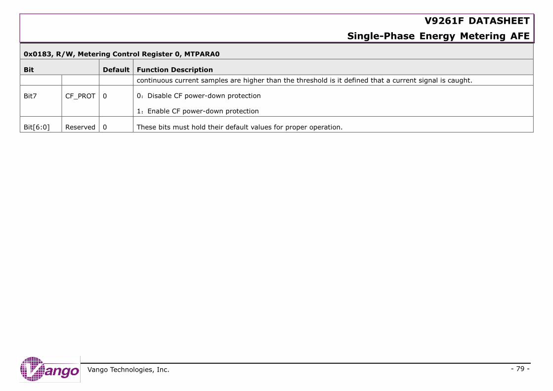
V9261F DATASHEET
Single-Phase Energy Metering AFE
- 79 -
Vango Technologies, Inc.
0x0183, R/W, Metering Control Register 0, MTPARA0
Bit Default Function Description
continuous current samples are higher than the threshold is it defined that a current signal is caught.
Bit7 CF_PROT 0 0:Disable CF power-down protection
1:Enable CF power-down protection
Bit[6:0] Reserved 0 These bits must hold their default values for proper operation.
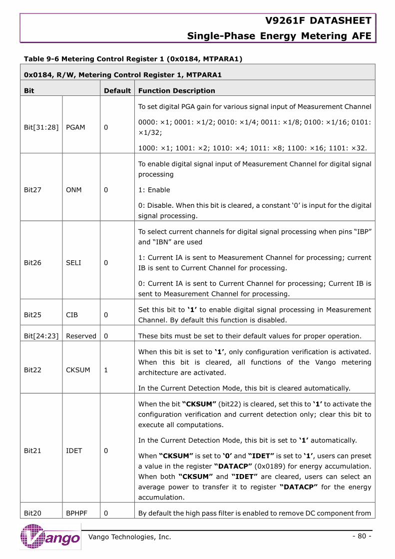
V9261F DATASHEET
Single-Phase Energy Metering AFE
- 80 -
Vango Technologies, Inc.
Table 9-6 Metering Control Register 1 (0x0184, MTPARA1)
0x0184, R/W, Metering Control Register 1, MTPARA1
Bit Default Function Description
Bit[31:28] PGAM 0
To set digital PGA gain for various signal input of Measurement Channel
0000: ×1; 0001: ×1/2; 0010: ×1/4; 0011: ×1/8; 0100: ×1/16; 0101:
×1/32;
1000: ×1; 1001: ×2; 1010: ×4; 1011: ×8; 1100: ×16; 1101: ×32.
Bit27 ONM 0
To enable digital signal input of Measurement Channel for digital signal
processing
1: Enable
0: Disable. When this bit is cleared, a constant ‘0’ is input for the digital
signal processing.
Bit26 SELI 0
To select current channels for digital signal processing when pins “IBP”
and “IBN” are used
1: Current IA is sent to Measurement Channel for processing; current
IB is sent to Current Channel for processing.
0: Current IA is sent to Current Channel for processing; Current IB is
sent to Measurement Channel for processing.
Bit25 CIB 0 Set this bit to ‘1’ to enable digital signal processing in Measurement
Channel. By default this function is disabled.
Bit[24:23] Reserved 0 These bits must be set to their default values for proper operation.
Bit22 CKSUM 1
When this bit is set to ‘1’, only configuration verification is activated.
When this bit is cleared, all functions of the Vango metering
architecture are activated.
In the Current Detection Mode, this bit is cleared automatically.
Bit21 IDET 0
When the bit “CKSUM” (bit22) is cleared, set this to ‘1’ to activate the
configuration verification and current detection only; clear this bit to
execute all computations.
In the Current Detection Mode, this bit is set to ‘1’ automatically.
When “CKSUM” is set to ‘0’ and “IDET” is set to ‘1’, users can preset
a value in the register “DATACP” (0x0189) for energy accumulation.
When both “CKSUM” and “IDET” are cleared, users can select an
average power to transfer it to register “DATACP” for the energy
accumulation.
Bit20 BPHPF 0 By default the high pass filter is enabled to remove DC component from
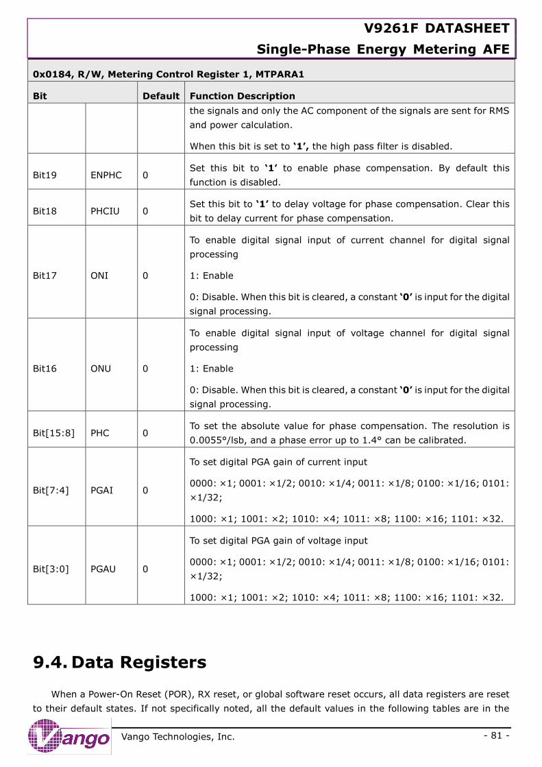
V9261F DATASHEET
Single-Phase Energy Metering AFE
- 81 -
Vango Technologies, Inc.
0x0184, R/W, Metering Control Register 1, MTPARA1
Bit Default Function Description
the signals and only the AC component of the signals are sent for RMS
and power calculation.
When this bit is set to ‘1’, the high pass filter is disabled.
Bit19 ENPHC 0 Set this bit to ‘1’ to enable phase compensation. By default this
function is disabled.
Bit18 PHCIU 0 Set this bit to ‘1’ to delay voltage for phase compensation. Clear this
bit to delay current for phase compensation.
Bit17 ONI 0
To enable digital signal input of current channel for digital signal
processing
1: Enable
0: Disable. When this bit is cleared, a constant ‘0’ is input for the digital
signal processing.
Bit16 ONU 0
To enable digital signal input of voltage channel for digital signal
processing
1: Enable
0: Disable. When this bit is cleared, a constant ‘0’ is input for the digital
signal processing.
Bit[15:8] PHC 0 To set the absolute value for phase compensation. The resolution is
0.0055°/lsb, and a phase error up to 1.4° can be calibrated.
Bit[7:4] PGAI 0
To set digital PGA gain of current input
0000: ×1; 0001: ×1/2; 0010: ×1/4; 0011: ×1/8; 0100: ×1/16; 0101:
×1/32;
1000: ×1; 1001: ×2; 1010: ×4; 1011: ×8; 1100: ×16; 1101: ×32.
Bit[3:0] PGAU 0
To set digital PGA gain of voltage input
0000: ×1; 0001: ×1/2; 0010: ×1/4; 0011: ×1/8; 0100: ×1/16; 0101:
×1/32;
1000: ×1; 1001: ×2; 1010: ×4; 1011: ×8; 1100: ×16; 1101: ×32.
9.4. Data Registers
When a Power-On Reset (POR), RX reset, or global software reset occurs, all data registers are reset
to their default states. If not specifically noted, all the default values in the following tables are in the
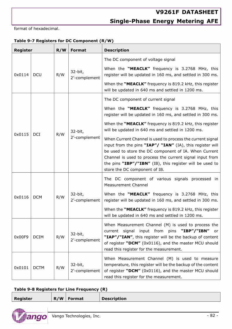
V9261F DATASHEET
Single-Phase Energy Metering AFE
- 82 -
Vango Technologies, Inc.
format of hexadecimal.
Table 9-7 Registers for DC Component (R/W)
Register R/W Format Description
0x0114 DCU R/W 32-bit,
2’-complement
The DC component of voltage signal
When the “MEACLK” frequency is 3.2768 MHz, this
register will be updated in 160 ms, and settled in 300 ms.
When the “MEACLK” frequency is 819.2 kHz, this register
will be updated in 640 ms and settled in 1200 ms.
0x0115 DCI R/W 32-bit,
2’-complement
The DC component of current signal
When the “MEACLK” frequency is 3.2768 MHz, this
register will be updated in 160 ms, and settled in 300 ms.
When the “MEACLK” frequency is 819.2 kHz, this register
will be updated in 640 ms and settled in 1200 ms.
When Current Channel is used to process the current signal
input from the pins “IAP”/ “IAN” (IA), this register will
be used to store the DC component of IA. When Current
Channel is used to process the current signal input from
the pins “IBP”/“IBN” (IB), this register will be used to
store the DC component of IB.
0x0116 DCM R/W 32-bit,
2’-complement
The DC component of various signals processed in
Measurement Channel
When the “MEACLK” frequency is 3.2768 MHz, this
register will be updated in 160 ms, and settled in 300 ms.
When the “MEACLK” frequency is 819.2 kHz, this register
will be updated in 640 ms and settled in 1200 ms.
0x00F9 DCIM R/W 32-bit,
2’-complement
When Measurement Channel (M) is used to process the
current signal input from pins “IBP”/“IBN” or
“IAP”/“IAN”, this register will be the backup of content
of register “DCM” (0x0116), and the master MCU should
read this register for the measurement.
0x0101 DCTM R/W 32-bit,
2’-complement
When Measurement Channel (M) is used to measure
temperature, this register will be the backup of the content
of register “DCM” (0x0116), and the master MCU should
read this register for the measurement.
Table 9-8 Registers for Line Frequency (R)
Register R/W Format Description
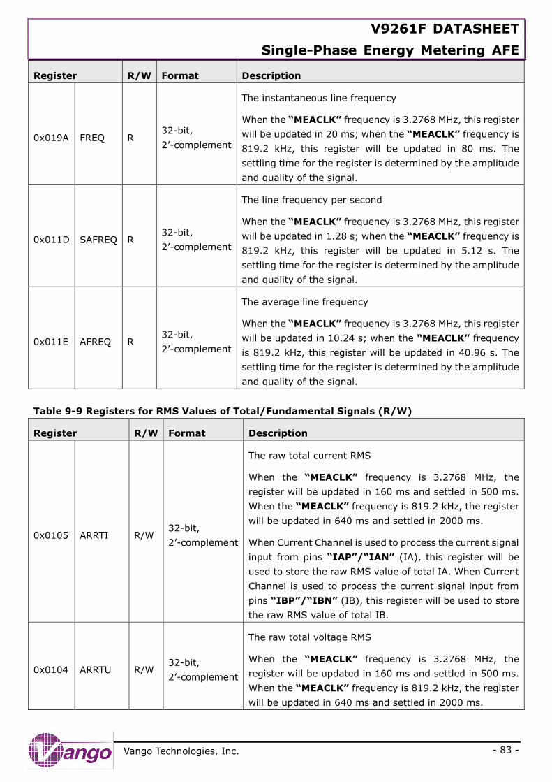
V9261F DATASHEET
Single-Phase Energy Metering AFE
- 83 -
Vango Technologies, Inc.
Register R/W Format Description
0x019A FREQ R 32-bit,
2’-complement
The instantaneous line frequency
When the “MEACLK” frequency is 3.2768 MHz, this register
will be updated in 20 ms; when the “MEACLK” frequency is
819.2 kHz, this register will be updated in 80 ms. The
settling time for the register is determined by the amplitude
and quality of the signal.
0x011D SAFREQ R 32-bit,
2’-complement
The line frequency per second
When the “MEACLK” frequency is 3.2768 MHz, this register
will be updated in 1.28 s; when the “MEACLK” frequency is
819.2 kHz, this register will be updated in 5.12 s. The
settling time for the register is determined by the amplitude
and quality of the signal.
0x011E AFREQ R 32-bit,
2’-complement
The average line frequency
When the “MEACLK” frequency is 3.2768 MHz, this register
will be updated in 10.24 s; when the “MEACLK” frequency
is 819.2 kHz, this register will be updated in 40.96 s. The
settling time for the register is determined by the amplitude
and quality of the signal.
Table 9-9 Registers for RMS Values of Total/Fundamental Signals (R/W)
Register R/W Format Description
0x0105 ARRTI R/W 32-bit,
2’-complement
The raw total current RMS
When the “MEACLK” frequency is 3.2768 MHz, the
register will be updated in 160 ms and settled in 500 ms.
When the “MEACLK” frequency is 819.2 kHz, the register
will be updated in 640 ms and settled in 2000 ms.
When Current Channel is used to process the current signal
input from pins “IAP”/“IAN” (IA), this register will be
used to store the raw RMS value of total IA. When Current
Channel is used to process the current signal input from
pins “IBP”/“IBN” (IB), this register will be used to store
the raw RMS value of total IB.
0x0104 ARRTU R/W 32-bit,
2’-complement
The raw total voltage RMS
When the “MEACLK” frequency is 3.2768 MHz, the
register will be updated in 160 ms and settled in 500 ms.
When the “MEACLK” frequency is 819.2 kHz, the register
will be updated in 640 ms and settled in 2000 ms.
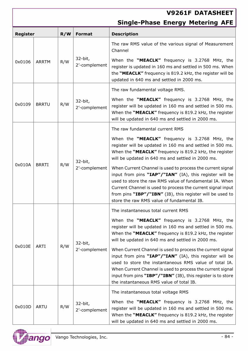
V9261F DATASHEET
Single-Phase Energy Metering AFE
- 84 -
Vango Technologies, Inc.
Register R/W Format Description
0x0106 ARRTM R/W 32-bit,
2’-complement
The raw RMS value of the various signal of Measurement
Channel
When the “MEACLK” frequency is 3.2768 MHz, the
register is updated in 160 ms and settled in 500 ms. When
the “MEACLK” frequency is 819.2 kHz, the register will be
updated in 640 ms and settled in 2000 ms.
0x0109 BRRTU R/W 32-bit,
2’-complement
The raw fundamental voltage RMS.
When the “MEACLK” frequency is 3.2768 MHz, the
register will be updated in 160 ms and settled in 500 ms.
When the “MEACLK” frequency is 819.2 kHz, the register
will be updated in 640 ms and settled in 2000 ms.
0x010A BRRTI R/W 32-bit,
2’-complement
The raw fundamental current RMS
When the “MEACLK” frequency is 3.2768 MHz, the
register will be updated in 160 ms and settled in 500 ms.
When the “MEACLK” frequency is 819.2 kHz, the register
will be updated in 640 ms and settled in 2000 ms.
When Current Channel is used to process the current signal
input from pins “IAP”/“IAN” (IA), this register will be
used to store the raw RMS value of fundamental IA. When
Current Channel is used to process the current signal input
from pins “IBP”/“IBN” (IB), this register will be used to
store the raw RMS value of fundamental IB.
0x010E ARTI R/W 32-bit,
2’-complement
The instantaneous total current RMS
When the “MEACLK” frequency is 3.2768 MHz, the
register will be updated in 160 ms and settled in 500 ms.
When the “MEACLK” frequency is 819.2 kHz, the register
will be updated in 640 ms and settled in 2000 ms.
When Current Channel is used to process the current signal
input from pins “IAP”/“IAN” (IA), this register will be
used to store the instantaneous RMS value of total IA.
When Current Channel is used to process the current signal
input from pins “IBP”/“IBN” (IB), this register is to store
the instantaneous RMS value of total IB.
0x010D ARTU R/W 32-bit,
2’-complement
The instantaneous total voltage RMS
When the “MEACLK” frequency is 3.2768 MHz, the
register will be updated in 160 ms and settled in 500 ms.
When the “MEACLK” frequency is 819.2 kHz, the register
will be updated in 640 ms and settled in 2000 ms.
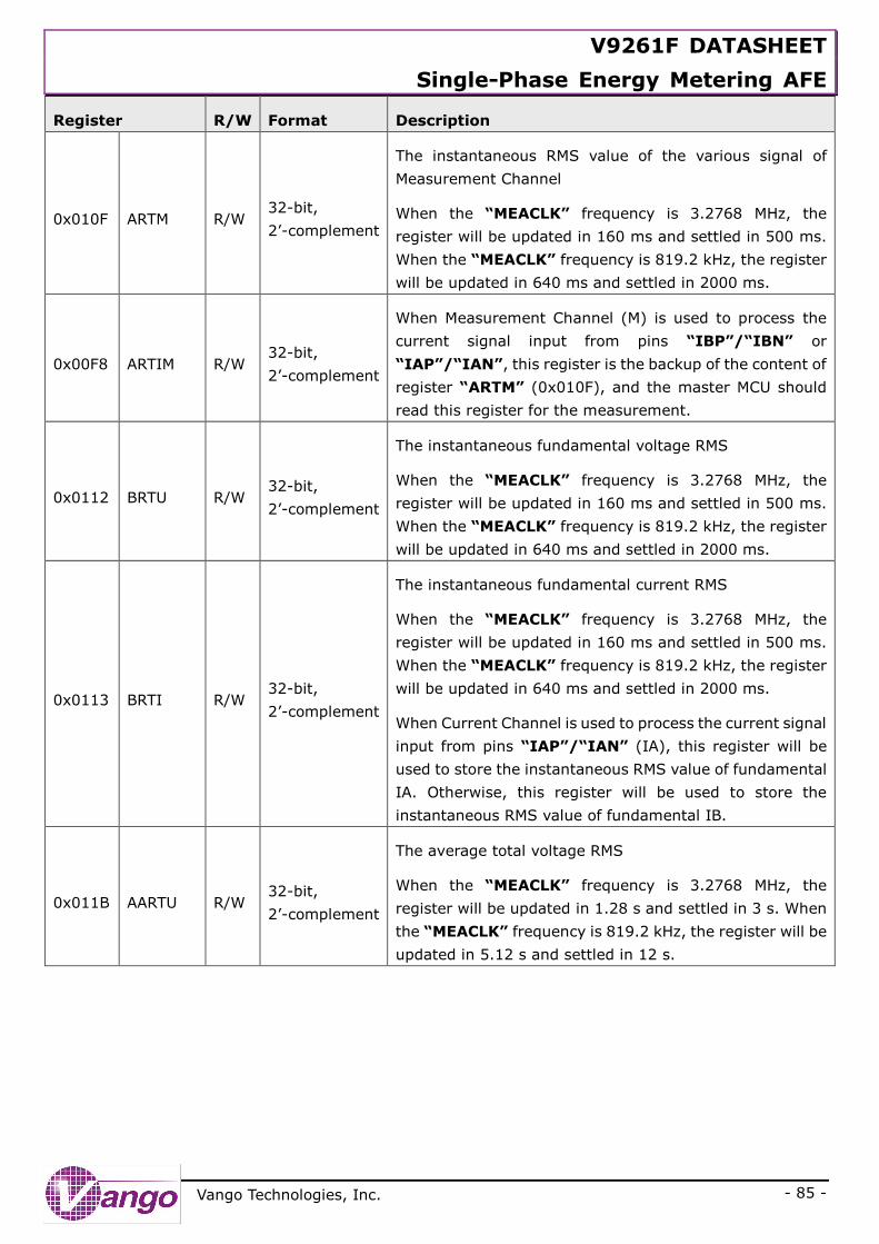
V9261F DATASHEET
Single-Phase Energy Metering AFE
- 85 -
Vango Technologies, Inc.
Register R/W Format Description
0x010F ARTM R/W 32-bit,
2’-complement
The instantaneous RMS value of the various signal of
Measurement Channel
When the “MEACLK” frequency is 3.2768 MHz, the
register will be updated in 160 ms and settled in 500 ms.
When the “MEACLK” frequency is 819.2 kHz, the register
will be updated in 640 ms and settled in 2000 ms.
0x00F8 ARTIM R/W 32-bit,
2’-complement
When Measurement Channel (M) is used to process the
current signal input from pins “IBP”/“IBN” or
“IAP”/“IAN”, this register is the backup of the content of
register “ARTM” (0x010F), and the master MCU should
read this register for the measurement.
0x0112 BRTU R/W 32-bit,
2’-complement
The instantaneous fundamental voltage RMS
When the “MEACLK” frequency is 3.2768 MHz, the
register will be updated in 160 ms and settled in 500 ms.
When the “MEACLK” frequency is 819.2 kHz, the register
will be updated in 640 ms and settled in 2000 ms.
0x0113 BRTI R/W 32-bit,
2’-complement
The instantaneous fundamental current RMS
When the “MEACLK” frequency is 3.2768 MHz, the
register will be updated in 160 ms and settled in 500 ms.
When the “MEACLK” frequency is 819.2 kHz, the register
will be updated in 640 ms and settled in 2000 ms.
When Current Channel is used to process the current signal
input from pins “IAP”/“IAN” (IA), this register will be
used to store the instantaneous RMS value of fundamental
IA. Otherwise, this register will be used to store the
instantaneous RMS value of fundamental IB.
0x011B AARTU R/W 32-bit,
2’-complement
The average total voltage RMS
When the “MEACLK” frequency is 3.2768 MHz, the
register will be updated in 1.28 s and settled in 3 s. When
the “MEACLK” frequency is 819.2 kHz, the register will be
updated in 5.12 s and settled in 12 s.
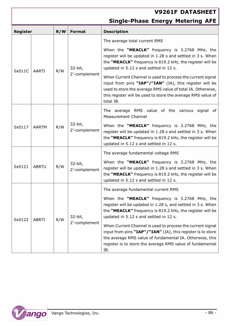
V9261F DATASHEET
Single-Phase Energy Metering AFE
- 86 -
Vango Technologies, Inc.
Register R/W Format Description
0x011C AARTI R/W 32-bit,
2’-complement
The average total current RMS
When the “MEACLK” frequency is 3.2768 MHz, the
register will be updated in 1.28 s and settled in 3 s. When
the “MEACLK” frequency is 819.2 kHz, the register will be
updated in 5.12 s and settled in 12 s.
When Current Channel is used to process the current signal
input from pins “IAP”/“IAN” (IA), this register will be
used to store the average RMS value of total IA. Otherwise,
this register will be used to store the average RMS value of
total IB.
0x0117 AARTM R/W 32-bit,
2’-complement
The average RMS value of the various signal of
Measurement Channel
When the “MEACLK” frequency is 3.2768 MHz, the
register will be updated in 1.28 s and settled in 3 s. When
the “MEACLK” frequency is 819.2 kHz, the register will be
updated in 5.12 s and settled in 12 s.
0x0121 ABRTU R/W 32-bit,
2’-complement
The average fundamental voltage RMS
When the “MEACLK” frequency is 3.2768 MHz, the
register will be updated in 1.28 s and settled in 3 s. When
the “MEACLK” frequency is 819.2 kHz, the register will be
updated in 5.12 s and settled in 12 s.
0x0122 ABRTI R/W 32-bit,
2’-complement
The average fundamental current RMS
When the “MEACLK” frequency is 3.2768 MHz, the
register will be updated in 1.28 s, and settled in 3 s. When
the “MEACLK” frequency is 819.2 kHz, the register will be
updated in 5.12 s and settled in 12 s.
When Current Channel is used to process the current signal
input from pins “IAP”/“IAN” (IA), this register is to store
the average RMS value of fundamental IA. Otherwise, this
register is to store the average RMS value of fundamental
IB.
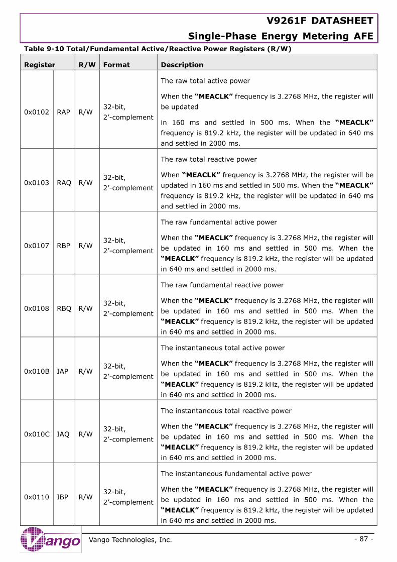
V9261F DATASHEET
Single-Phase Energy Metering AFE
- 87 -
Vango Technologies, Inc.
Table 9-10 Total/Fundamental Active/Reactive Power Registers (R/W)
Register R/W Format Description
0x0102 RAP R/W 32-bit,
2’-complement
The raw total active power
When the “MEACLK” frequency is 3.2768 MHz, the register will
be updated
in 160 ms and settled in 500 ms. When the “MEACLK”
frequency is 819.2 kHz, the register will be updated in 640 ms
and settled in 2000 ms.
0x0103 RAQ R/W 32-bit,
2’-complement
The raw total reactive power
When “MEACLK” frequency is 3.2768 MHz, the register will be
updated in 160 ms and settled in 500 ms. When the “MEACLK”
frequency is 819.2 kHz, the register will be updated in 640 ms
and settled in 2000 ms.
0x0107 RBP R/W 32-bit,
2’-complement
The raw fundamental active power
When the “MEACLK” frequency is 3.2768 MHz, the register will
be updated in 160 ms and settled in 500 ms. When the
“MEACLK” frequency is 819.2 kHz, the register will be updated
in 640 ms and settled in 2000 ms.
0x0108 RBQ R/W 32-bit,
2’-complement
The raw fundamental reactive power
When the “MEACLK” frequency is 3.2768 MHz, the register will
be updated in 160 ms and settled in 500 ms. When the
“MEACLK” frequency is 819.2 kHz, the register will be updated
in 640 ms and settled in 2000 ms.
0x010B IAP R/W 32-bit,
2’-complement
The instantaneous total active power
When the “MEACLK” frequency is 3.2768 MHz, the register will
be updated in 160 ms and settled in 500 ms. When the
“MEACLK” frequency is 819.2 kHz, the register will be updated
in 640 ms and settled in 2000 ms.
0x010C IAQ R/W 32-bit,
2’-complement
The instantaneous total reactive power
When the “MEACLK” frequency is 3.2768 MHz, the register will
be updated in 160 ms and settled in 500 ms. When the
“MEACLK” frequency is 819.2 kHz, the register will be updated
in 640 ms and settled in 2000 ms.
0x0110 IBP R/W 32-bit,
2’-complement
The instantaneous fundamental active power
When the “MEACLK” frequency is 3.2768 MHz, the register will
be updated in 160 ms and settled in 500 ms. When the
“MEACLK” frequency is 819.2 kHz, the register will be updated
in 640 ms and settled in 2000 ms.
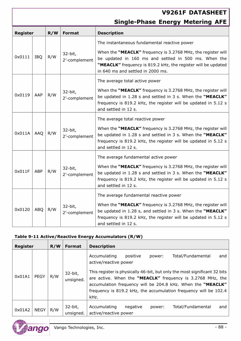
V9261F DATASHEET
Single-Phase Energy Metering AFE
- 88 -
Vango Technologies, Inc.
Register R/W Format Description
0x0111 IBQ R/W 32-bit,
2’-complement
The instantaneous fundamental reactive power
When the “MEACLK” frequency is 3.2768 MHz, the register will
be updated in 160 ms and settled in 500 ms. When the
“MEACLK” frequency is 819.2 kHz, the register will be updated
in 640 ms and settled in 2000 ms.
0x0119 AAP R/W 32-bit,
2’-complement
The average total active power
When the “MEACLK” frequency is 3.2768 MHz, the register will
be updated in 1.28 s and settled in 3 s. When the “MEACLK”
frequency is 819.2 kHz, the register will be updated in 5.12 s
and settled in 12 s.
0x011A AAQ R/W 32-bit,
2’-complement
The average total reactive power
When the “MEACLK” frequency is 3.2768 MHz, the register will
be updated in 1.28 s and settled in 3 s. When the “MEACLK”
frequency is 819.2 kHz, the register will be updated in 5.12 s
and settled in 12 s.
0x011F ABP R/W 32-bit,
2’-complement
The average fundamental active power
When the “MEACLK” frequency is 3.2768 MHz, the register will
be updated in 1.28 s and settled in 3 s. When the “MEACLK”
frequency is 819.2 kHz, the register will be updated in 5.12 s
and settled in 12 s.
0x0120 ABQ R/W 32-bit,
2’-complement
The average fundamental reactive power
When the “MEACLK” frequency is 3.2768 MHz, the register will
be updated in 1.28 s, and settled in 3 s. When the “MEACLK”
frequency is 819.2 kHz, the register will be updated in 5.12 s
and settled in 12 s.
Table 9-11 Active/Reactive Energy Accumulators (R/W)
Register R/W Format Description
0x01A1 PEGY R/W 32-bit,
unsigned.
Accumulating positive power: Total/Fundamental and
active/reactive power
This register is physically 46-bit, but only the most significant 32 bits
are active. When the “MEACLK” frequency is 3.2768 MHz, the
accumulation frequency will be 204.8 kHz. When the “MEACLK”
frequency is 819.2 kHz, the accumulation frequency will be 102.4
kHz.
0x01A2 NEGY R/W 32-bit,
unsigned.
Accumulating negative power: Total/Fundamental and
active/reactive power
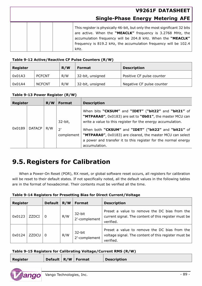
V9261F DATASHEET
Single-Phase Energy Metering AFE
- 89 -
Vango Technologies, Inc.
This register is physically 46-bit, but only the most significant 32 bits
are active. When the “MEACLK” frequency is 3.2768 MHz, the
accumulation frequency will be 204.8 kHz. When the “MEACLK”
frequency is 819.2 kHz, the accumulation frequency will be 102.4
kHz.
Table 9-12 Active/Reactive CF Pulse Counters (R/W)
Register R/W Format Description
0x01A3 PCFCNT R/W 32-bit, unsigned Positive CF pulse counter
0x01A4 NCFCNT R/W 32-bit, unsigned Negative CF pulse counter
Table 9-13 Power Register (R/W)
Register R/W Format Description
0x0189 DATACP R/W
32-bit,
2’
complement
When bits “CKSUM” and “IDET” (“bit22” and “bit21” of
“MTPARA0”, 0x0183) are set to “0b01”, the master MCU can
write a value to this register for the energy accumulation.
When both “CKSUM” and “IDET” (“bit22” and “bit21” of
“MTPARA0”, 0x0183) are cleared, the master MCU can select
a power and transfer it to this register for the normal energy
accumulation.
9.5. Registers for Calibration
When a Power-On Reset (POR), RX reset, or global software reset occurs, all registers for calibration
will be reset to their default states. If not specifically noted, all the default values in the following tables
are in the format of hexadecimal. Their contents must be verified all the time.
Table 9-14 Registers for Presetting Bias for Direct Current/Voltage
Register Default R/W Format Description
0x0123 ZZDCI 0 R/W 32-bit
2’-complement
Preset a value to remove the DC bias from the
current signal. The content of this register must be
verified.
0x0124 ZZDCU 0 R/W 32-bit
2’-complement
Preset a value to remove the DC bias from the
voltage signal. The content of this register must be
verified.
Table 9-15 Registers for Calibrating Voltage/Current RMS (R/W)
Register Default R/W Format Description
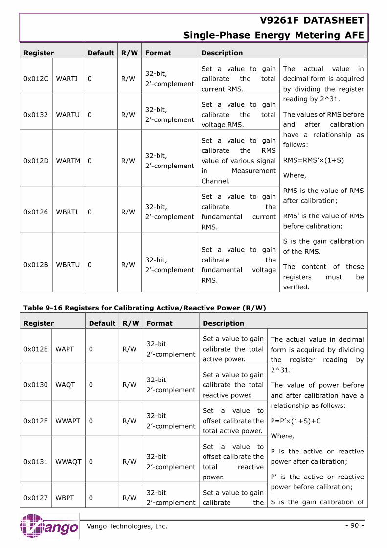
V9261F DATASHEET
Single-Phase Energy Metering AFE
- 90 -
Vango Technologies, Inc.
Register Default R/W Format Description
0x012C WARTI 0 R/W 32-bit,
2’-complement
Set a value to gain
calibrate the total
current RMS.
The actual value in
decimal form is acquired
by dividing the register
reading by 2^31.
The values of RMS before
and after calibration
have a relationship as
follows:
RMS=RMS’×(1+S)
Where,
RMS is the value of RMS
after calibration;
RMS’ is the value of RMS
before calibration;
S is the gain calibration
of the RMS.
The content of these
registers must be
verified.
0x0132 WARTU 0 R/W 32-bit,
2’-complement
Set a value to gain
calibrate the total
voltage RMS.
0x012D WARTM 0 R/W 32-bit,
2’-complement
Set a value to gain
calibrate the RMS
value of various signal
in Measurement
Channel.
0x0126 WBRTI 0 R/W 32-bit,
2’-complement
Set a value to gain
calibrate the
fundamental current
RMS.
0x012B WBRTU 0 R/W 32-bit,
2’-complement
Set a value to gain
calibrate the
fundamental voltage
RMS.
Table 9-16 Registers for Calibrating Active/Reactive Power (R/W)
Register Default R/W Format Description
0x012E WAPT 0 R/W 32-bit
2’-complement
Set a value to gain
calibrate the total
active power.
The actual value in decimal
form is acquired by dividing
the register reading by
2^31.
The value of power before
and after calibration have a
relationship as follows:
P=P’×(1+S)+C
Where,
P is the active or reactive
power after calibration;
P’ is the active or reactive
power before calibration;
S is the gain calibration of
0x0130 WAQT 0 R/W 32-bit
2’-complement
Set a value to gain
calibrate the total
reactive power.
0x012F WWAPT 0 R/W 32-bit
2’-complement
Set a value to
offset calibrate the
total active power.
0x0131 WWAQT 0 R/W 32-bit
2’-complement
Set a value to
offset calibrate the
total reactive
power.
0x0127 WBPT 0 R/W 32-bit
2’-complement
Set a value to gain
calibrate the
V9261F DATASHEET
Single-Phase Energy Metering AFE
- 91 -
Vango Technologies, Inc.
Register Default R/W Format Description
fundamental
active power.
the power;
C is the offset calibration of
the power.
The content of these
registers must be verified.
0x0129 WBQT 0 R/W 32-bit
2’-complement
Set a value to gain
calibrate the
fundamental
reactive power.
0x0128 WWBPT 0 R/W 32-bit
2’-complement
Set a value to
offset calibrate the
fundamental
active power.
0x012A WWBQT 0 R/W 32-bit
2’-complement
Set a value to
offset calibrate the
fundamental
reactive power.
Table 9-17 Threshold Register
Register Default R/W Format Description
0x0181 EGYTH 0 R/W 32-bit,
2’-complement
Set a threshold for energy-to-pulse conversion.
The content of this register must be verified.
0x0182 CTH 0 R/W 32-bit,
2’-complement
Set a threshold for no-load detection. The content
of this register must be verified.
0x0134 IDETTH 0 R/W 32-bit
2’-complement
Set a threshold for current detection.
When the current detection is enabled, the current
detection circuit will compare the absolute value of
the instantaneous current signal to the preset
current detection threshold in this register. When
some continuous samples of the current signal are
higher than the threshold, it means a current
signal is caught.
The content of this register must be verified.
Table 9-18 Register for Bandpass Filter Coefficient Configuration (0x0125, BPFPARA, R/W)
Register Default R/W Format Description
0x0125 BPFPARA 0 R/W 32-bit
2’-complement
Set the coefficient of the bandpass filter.
Generally, it is set to “0x811D2BA7” for the
best performance.
This coefficient and the bits to be shift in the
bandpass filter have effects on filter response
V9261F DATASHEET
Single-Phase Energy Metering AFE
- 92 -
Vango Technologies, Inc.
Register Default R/W Format Description
time, the sensitivity to the frequency deviation,
and the suppression on the harmonics and noise.
The content of this register must be verified.
9.6. Checksum Register
Table 9-19 Checksum Register (0x0133, CKSUM, R/W)
Register Default R/W Format Description
0x0133 CKSUM 0 R/W 32-bit
2’-complement
Add the value of this register and other 24
registers (Including metering control registers,
analog control registers, and registers for
calibration, see “Interrupt” for details) to
compute the checksum for configuration
verification to ensure the configuration of all the
registers are in the desired states. If the sum is
“0xFFFFFFFF”, the verification will pass.
This register should be set to the difference of
“0xFFFFFFFF” and the sum of the other 24
registers.
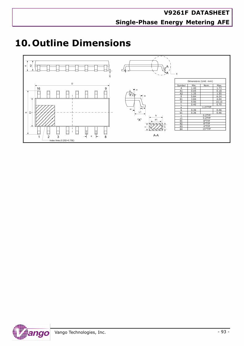
V9261F DATASHEET
Single-Phase Energy Metering AFE
- 93 -
Vango Technologies, Inc.
10. Outline Dimensions
E E1
D
e
A A2
A1
θ3
L1
L
θ4
θ1
h
h
θ2
A
A
b
b1
c
Index Area (0.25D+0.75E)
1 2 3 8
916
X
c1
“X”
A-A
Symbol Min. Nom. Max.
A 1.40 1.73
A1 0.05 0.18
A2 1.35 1.55
E 5.84 6.24
E1 3.84 4.04
D 9.90 10.10
L 0.40 0.70
e
b 0.36 0.46
b1 0.36 0.46
c
c1
θ1
θ2
θ3
θ4 15°TYP
Dimensions (Unit: mm)
1.27TYP
0.2TYP
0.2TYP
8°TYP8°TYP
4°TYP