Embed Size (px)
Citation preview
The Instructions of WT588D-U Voice Module
www.elechouse.com
页-
-第 2
1、Product Features ............................................................................................................... 1 2、Functional Description ........................................................................... 3、Application scopes ............................................................................................................ 4 4、Application Block diagram .................................................................................................. 4 5、Pin Package Fig. ............................................................................................................... 5 6、Electrical Parameters......................................................................................................... 6 7、The Absolute Limits of The Environment Parameters............................................................ 7 8、Control Mode .................................................................................................................... 7
8.1、Button Control Mode ................................................................................................. 7 8.1.1、Tigger Impulse Repetition ................................................................................. 7 8.1.2、Trigger Impluse Without Repetition .................................................................... 8 8.1.3、Recycled Level ................................................................................................. 8 8.1.4、Nocycle Level .................................................................................................. 8 8.1.5、Non-Maintained Cycle Level .............................................................................. 9 8.1.6、Play / Stop ....................................................................................................... 9 8.1.7、Non-Cycle for The Next Tone............................................................................. 9 8.1.8、Non-Cycle for The Last Tone ........................................................................... 10 8.1.9、Recycle for The Next Tone .............................................................................. 10 8.1.10、Recycle for The Last Tone ............................................................................. 10 8.1.11、Pause .......................................................................................................... 11 8.1.12、Stop............................................................................................................. 11
8.2、One-Wire Serial Port Control Mode ......................................................................... 11 8.2.1、Port Allocation Table ....................................................................................... 11 8.2.2、Order and Speech Cording .............................................................................. 12 8.2.3、Voice Address Correspondence ....................................................................... 12 8.2.4、Control Time Sequence Chart.......................................................................... 12 8.2.5、The Example of 1-Wire Serial Port Control Time Sequence ............................... 13 8.2.6、Models of Procedure....................................................................................... 13
8.3、Three-Wire Serial Control mode ............................................................................... 14 8.3.1、Port Allocation Methods .................................................................................. 14 8.3.2、Voice and Command Code Corresponding to Table ........................................... 14 8.3.3、Voice Address Corresponds ............................................................................ 14 8.3.4、Three-Wire Serial Port Control Time Sequence................................................. 15 8.3.5、Modles of Procedure....................................................................................... 15
9、Typical Application Circuit ................................................................................................ 16 9.1、Typical Application Circuit of Key to Control(PWM output,5V Supply) ................... 16 9.2、Typical Application Circuit of Keys to Control(PWM output,3.3V Supply) .............. 16 9.3、Typical Application Circuit of Keys to Control(DAC output) .................................... 17 9.4、Typical Application of Frst-line Serial Cntrol Circuit (PWM Output) ........................... 17 9.5、Typical Application of First-line Serial Control Circuit(DAC Output) ........................ 17 9.6、0ne-Wire Serial Port MCU5V Power/ Module 3.3V Power Supply Application circuit (PWM output) ........................................................................................................................... 18
www.elechouse.com

页-
-第 3
9.7、Three-Wire Serial Control of Typical Application circuit (PWM output) ........................ 19 9.8、Three-wire serial control of a typical application circuit (DACoutput) .......................... 19 9.9、Three-wire serial MCU5V power / module 3.3V power supply application circuit (PWM output) MCU5V ............................................................................................................... 19
10、Control procedures ........................................................................................................ 20 10.1、One-wire serial control of assembler ...................................................................... 20 10.2、One-wire serial control of C-voice procedures ......................................................... 21 10.3、Three-wire serial control of assembler .................................................................... 23 10.4、Three-wire serial control of C-voice procedures ...................................................... 24
11、Package size Figure....................................................................................................... 26
1、Product features Package of 28 pins module, which can be replaced memory for gainting different lengths of storage
time. Support SPI-Flash, which ‘s capacity is 2M bit ~ 32M (Note: 1byte = 8bit) WT588D-20SS voice used as a control core chip. Embedded human voice processor, feel very natural and sweet. Good audio quality output for 13Bit/DA converter and 12Bit/PWM processing of audio. Support for loading 6K ~ 22KHz audio sampling rate. PWM output can directly promote 0.5W/8Ω speakers and plenty of current. Support DAC / PWM output Support for loading WAV audio format. Support key control mode, one-wire serial control mode, three-wire serial control mode. A variety of IO trigger ways can be seted to in button control mode. The way of BUSY signal output can be set in a random manner. Loading no more than 500 segments voice for editing. Address bit is controled by 220 segments voice, but a single address bit just can load up to 128. Voice player to enter the sleep mode to stop immediately. It is simple interface and convenient because of using WT588D Voice Chip that benefited to exert its
functions. A lot of operations can be finished in software. Such as setup control mode, inserting voice,
compositing voice, calling voice, etc. Free to insert mute, mute time range 10ms ~ 25min. Support online USB download / offline USB download. What’s more, it also can download data to
SPI-Flash even if WT588D-U are working. Operating voltage: DC2.8V ~ 5.5V.
www.elechouse.com
页-
-第 4
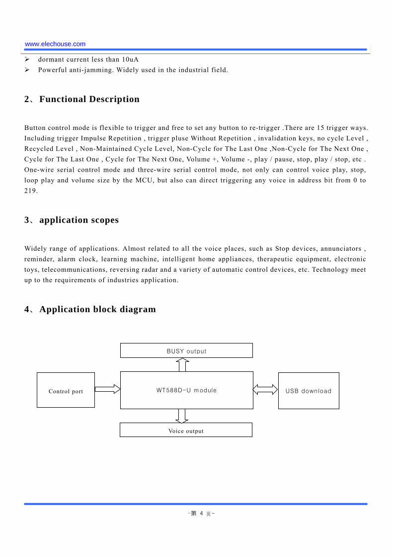
dormant current less than 10uA
Powerful anti-jamming. Widely used in the industrial field.
2、Functional Description
Button control mode is flexible to trigger and free to set any button to re-trigger .There are 15 trigger ways. Including trigger Impulse Repetition , trigger pluse Without Repetition , invalidation keys, no cycle Level , Recycled Level , Non-Maintained Cycle Level, Non-Cycle for The Last One ,Non-Cycle for The Next One , Cycle for The Last One , Cycle for The Next One, Volume +, Volume -, play / pause, stop, play / stop, etc . One-wire serial control mode and three-wire serial control mode, not only can control voice play, stop, loop play and volume size by the MCU, but also can direct triggering any voice in address bit from 0 to 219.
3、application scopes
Widely range of applications. Almost related to all the voice places, such as Stop devices, annunciators , reminder, alarm clock, learning machine, intelligent home appliances, therapeutic equipment, electronic toys, telecommunications, reversing radar and a variety of automatic control devices, etc. Technology meet up to the requirements of industries application.
4、Application block diagram
Control port
WT588D-U module
BUSY output
Voice output
USB download
www.elechouse.com
页-
-第 5
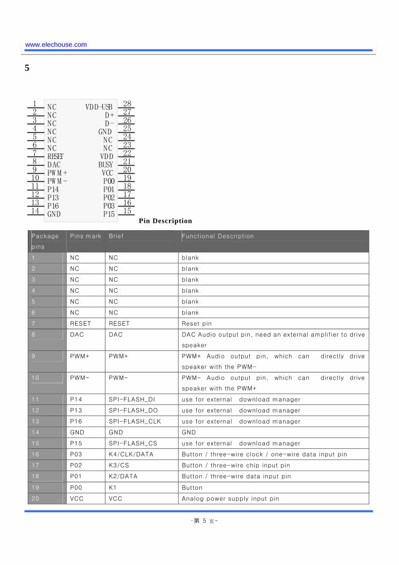
5
1234567891011121314 15
16171819202122232425262728NC
NCNCNCNCNCRESETDACPW M +PW M -P14P13P16GND P15
P03P02P01P00VCCBUSYVDDNCNC
GNDD-D+
VDD-USB
Pin Description
Package
pins
Pins mark Brief Functional Description
1 NC NC blank
2 NC NC blank
3 NC NC blank
4 NC NC blank
5 NC NC blank
6 NC NC blank
7 RESET RESET Reset pin
8 DAC DAC DAC Audio output pin, need an external amplifier to drive
speaker
9 PWM+ PWM+ PWM+ Audio output pin, which can directly drive
speaker with the PWM-
10 PWM- PWM- PWM- Audio output pin, which can directly drive
speaker with the PWM+
11 P14 SPI-FLASH_DI use for external download manager
12 P13 SPI-FLASH_DO use for external download manager
13 P16 SPI-FLASH_CLK use for external download manager
14 GND GND GND
15 P15 SPI-FLASH_CS use for external download manager
16 P03 K4/CLK/DATA Button / three-wire clock / one-wire data input pin
17 P02 K3/CS Button / three-wire chip input pin
18 P01 K2/DATA Button / three-wire data input pin
19 P00 K1 Button
20 VCC VCC Analog power supply input pin
www.elechouse.com
页-
-第 6
Note:Pin25,26,27,28 use to download for other USB slot.
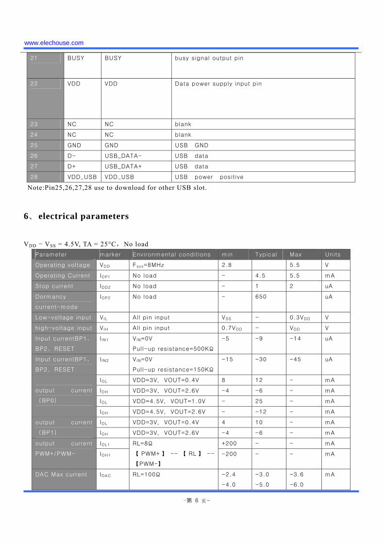
6、electrical parameters
VDD − VSS = 4.5V, TA = 25°C,No load Parameter marker Environmental conditions min Typical Max Units
Operating voltage VDD Fsys=8MHz 2.8 5.5 V
Operating Current IOP1 No load - 4.5 5.5 mA
Stop current IDD2 No load - 1 2 uA
Dormancy
current-mode
IOP2 No load - 650 uA
Low-voltage input VIL All pin input VSS - 0.3VDD V
high-voltage input VIH All pin input 0.7VDD - VDD V
Input currentBP1、
BP2、RESET
IIN1 VIN=0V
Pull-up resistance=500KΩ
-5 -9 -14 uA
Input currentBP1、
BP2、RESET
IIN2 VIN=0V
Pull-up resistance=150KΩ
-15 -30 -45 uA
IOL VDD=3V,VOUT=0.4V 8 12 - mA
IOH VDD=3V,VOUT=2.6V -4 -6 - mA
IOL VDD=4.5V,VOUT=1.0V - 25 - mA
output current
(BP0)
IOH VDD=4.5V,VOUT=2.6V - -12 - mA
IOL VDD=3V,VOUT=0.4V 4 10 - mA output current
(BP1) IOH VDD=3V,VOUT=2.6V -4 -6 - mA
IOL1 +200 - - mA output current
PWM+/PWM- IOH1
RL=8Ω
【 PWM+ 】 -- 【 RL 】 --
【PWM-】
-200 - - mA
DAC Max current IDAC RL=100Ω -2.4
-4.0
-3.0
-5.0
-3.6
-6.0
mA
21 BUSY BUSY busy signal output pin
22 VDD VDD Data power supply input pin
23 NC NC blank
24 NC NC blank
25 GND GND USB GND
26 D- USB_DATA- USB data
27 D+ USB_DATA+ USB data
28 VDD_USB VDD_USB USB power positive
www.elechouse.com
页-
-第 7
Pull-up resistor
test
RPL 75 150 225
7、Absolute limits of the environment parameters
parameters marker Environmental conditions
rating units
power VDD — VSS - -0.3~+7.0 V
Input voltage VIN input VSS-0.3~VDD+0.3 V
Storage temperature
TSTG - -55~+150 °C
Used temperature TOPR - -40~+85 °C
8、control mode
8.1、Buttons Control Mode
Pins can directly trigger a function of chip to work. Each pin of the trigger can be set individually. Shockproof time of this mode time is about 10ms. There are 15 trigger ways. Including trigger Impulse Repetition , trigger pluse Without Repetition , invalidation keys, no cycle Level , Recycled Level , Non-Maintained Cycle Level, Non-Cycle for The Last Tone ,Non-Cycle for The Next Tone , Cycle for The Last Tone , Cycle for The Next Tone, Volume +, Volume -, play / pause, stop, play / stop, etc. see the following trigger timing diagram. For more details, see the following chart:
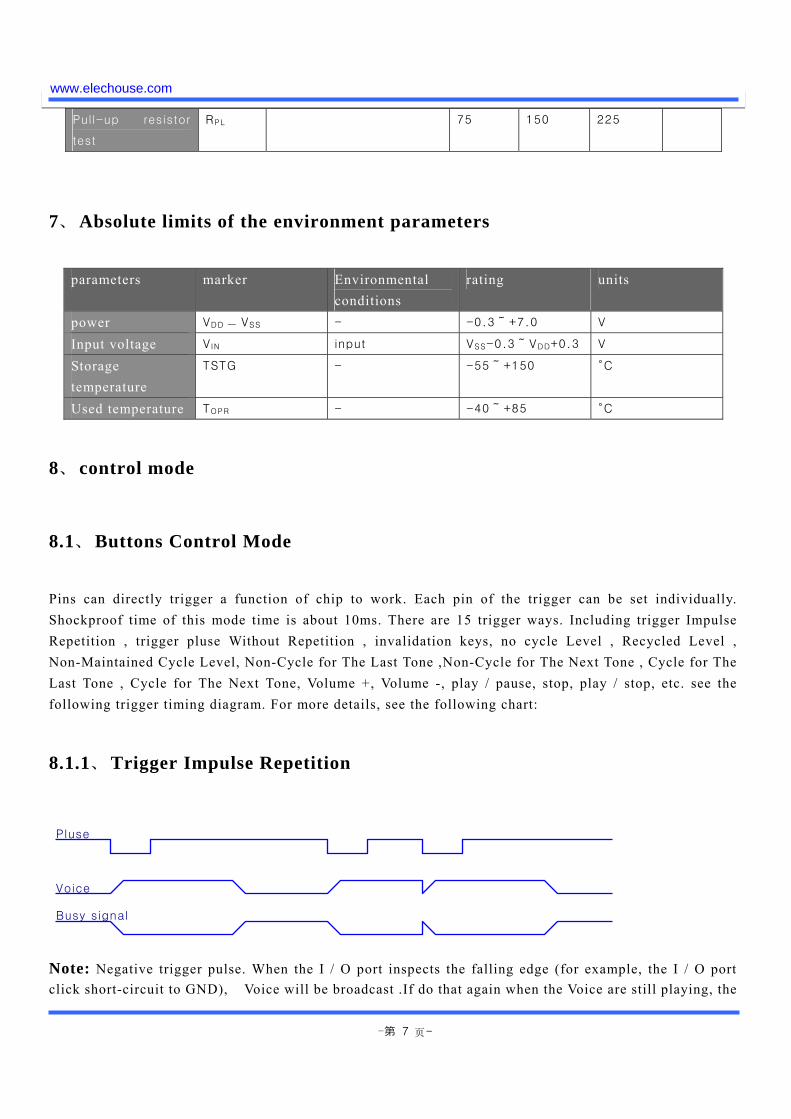
8.1.1、Trigger Impulse Repetition
Note: Negative trigger pulse. When the I / O port inspects the falling edge (for example, the I / O port click short-circuit to GND), Voice will be broadcast .If do that again when the Voice are still playing, the
Pluse
Voice
Busy signal
www.elechouse.com

页-
-第 8
voice will be interrupted and replay. Therefore, it will be replay as long as has falling edge signal.
8.1.2、Trigger Impluse Without Repetition
Note: Negative trigger pulse. When the I / O port inspects the falling edge (for example, the I / O port click short-circuit to GND), Voice will be broadcast. If do that again when the voice are still playing , the voice will not be interrupted and continue to broadcast. To be valid unless the voice at an end and inspects the falling edge.
8.1.3、Recycled Level
Note: High level stops when the I / O port is low and keep play. Continue to keep a low level even if the first time is over. It will go along replay until change into high level. Low level has sound. High level hasn’t.
8.1.4、No Cycle Level
Note: Trigger level. High level stops when the I / O port is low and keep play. I will be not Continue to play even if the first time is over and keep a low level. The voice just play one time after being triggered.
Pluse
Voice
Busy signal
level
Voice
Busy signal
Adress1 Address 1 Address 1
level
Voice
Busy signal
Address 1 Address 1
www.elechouse.com
页-
-第 9
If you need to replay, please make the I / O port at high level, and then pull low. Finally, keep it at low level .The end.
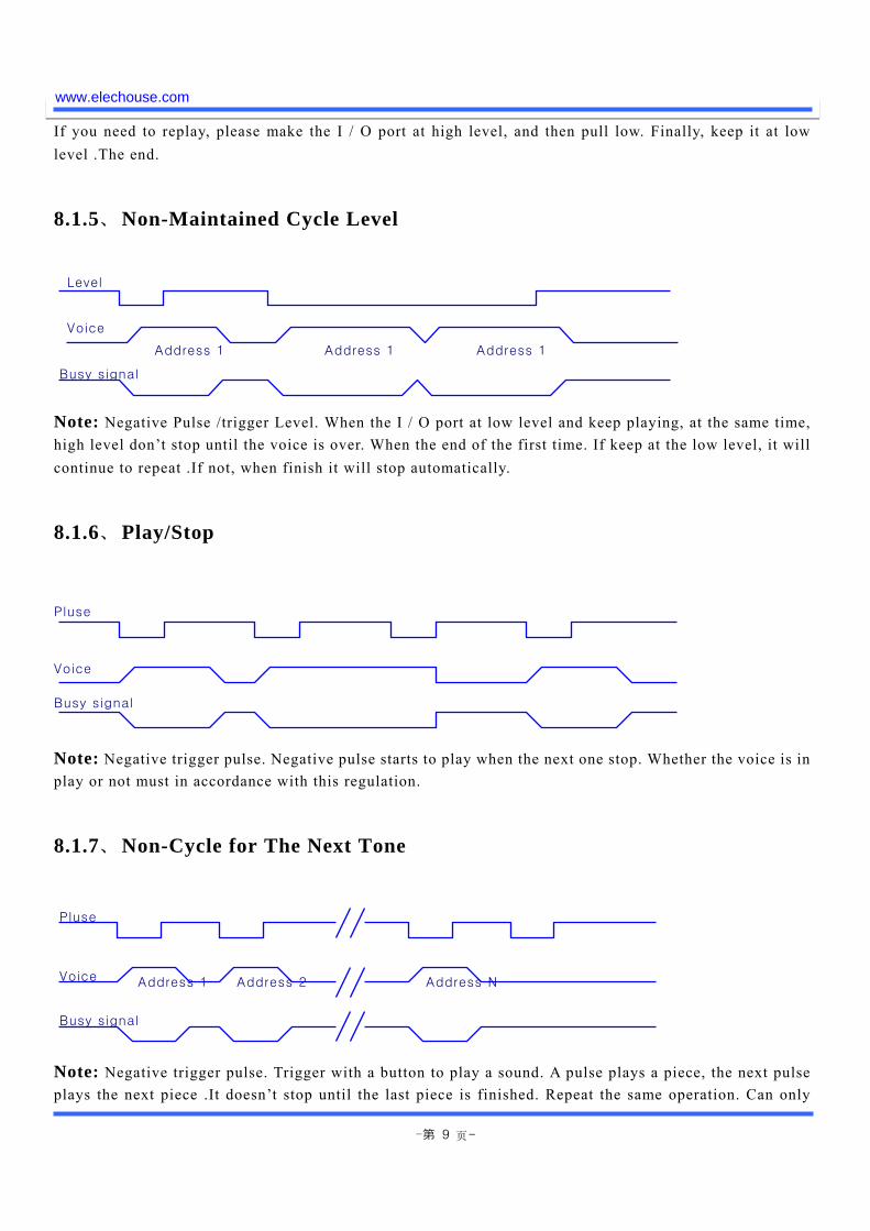
8.1.5、Non-Maintained Cycle Level
Note: Negative Pulse /trigger Level. When the I / O port at low level and keep playing, at the same time, high level don’t stop until the voice is over. When the end of the first time. If keep at the low level, it will continue to repeat .If not, when finish it will stop automatically.
8.1.6、Play/Stop
Note: Negative trigger pulse. Negative pulse starts to play when the next one stop. Whether the voice is in play or not must in accordance with this regulation.
8.1.7、Non-Cycle for The Next Tone
Note: Negative trigger pulse. Trigger with a button to play a sound. A pulse plays a piece, the next pulse plays the next piece .It doesn’t stop until the last piece is finished. Repeat the same operation. Can only
Level
Voice
Busy signal
Address 1 Address 1 Address 1
Voice
Busy signal
Pluse
Pluse
Voice
Busy signal
Address 1 Address 2 Address N
www.elechouse.com
页-
-第 10
play to the last.
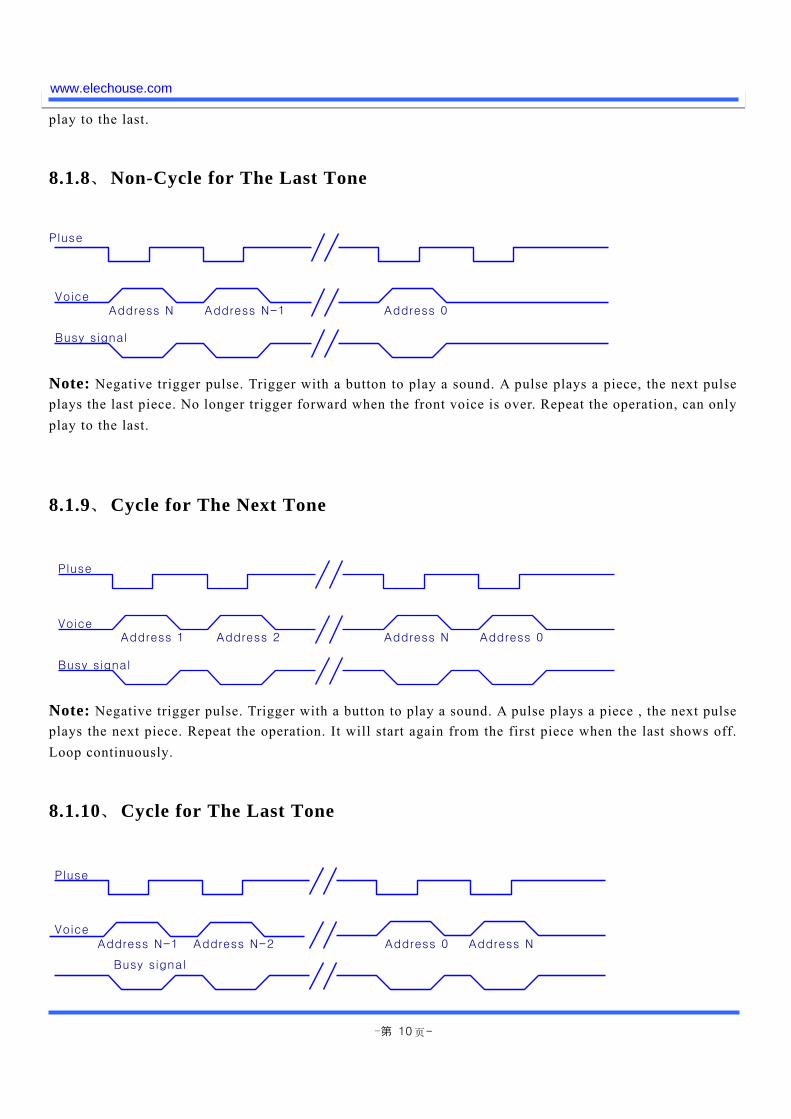
8.1.8、Non-Cycle for The Last Tone
Note: Negative trigger pulse. Trigger with a button to play a sound. A pulse plays a piece, the next pulse plays the last piece. No longer trigger forward when the front voice is over. Repeat the operation, can only play to the last.
8.1.9、Cycle for The Next Tone
Note: Negative trigger pulse. Trigger with a button to play a sound. A pulse plays a piece , the next pulse plays the next piece. Repeat the operation. It will start again from the first piece when the last shows off. Loop continuously.
8.1.10、Cycle for The Last Tone
Pluse
Voice
Busy signal
Address N Address N-1 Address 0
Pluse
Voice
Busy signal
Address 1 Address 2 Address N Address 0
Pluse
Voice Address N-1 Address N-2 Address 0 Address N
Busy signal
www.elechouse.com

页-
-第 11
Note: Negative trigger pulse. Trigger with a button to play a sound. A pulse plays a piece, the next pulse plays the last piece. Repeat the operation. It will start again from the last piece when the front shows off. Loop continuously.
8.1.11、Pause
Note: Negative trigger pulse. The first pulse voice is playing but in a suspended state. The second pulse still working, which triggers the suspension of the voice. BUSY remain in this state.
8.1.12、Stop
Note: Negative trigger pulse. Stopped the voice, which is playing . Trigger once again invalidly when the voice is stopped.
8.2、One-Wire Serial Port Control Mode
Send data through a data line. One-wire serial port can control voice play, stop, volume adjustment and directly trigger, etc. P00 ~ P02 I/O port can select screen or any trigger mode.
8.2.1、Port Allocation Table
I/O 口 P00 P01 P02 P03
Pluse
Voice
Busy signal Paused
Pluse
voice
Busy signal
www.elechouse.com
页-
-第 12
function Key-pressK1
Key-pressK2
Key-pressK3 DATA
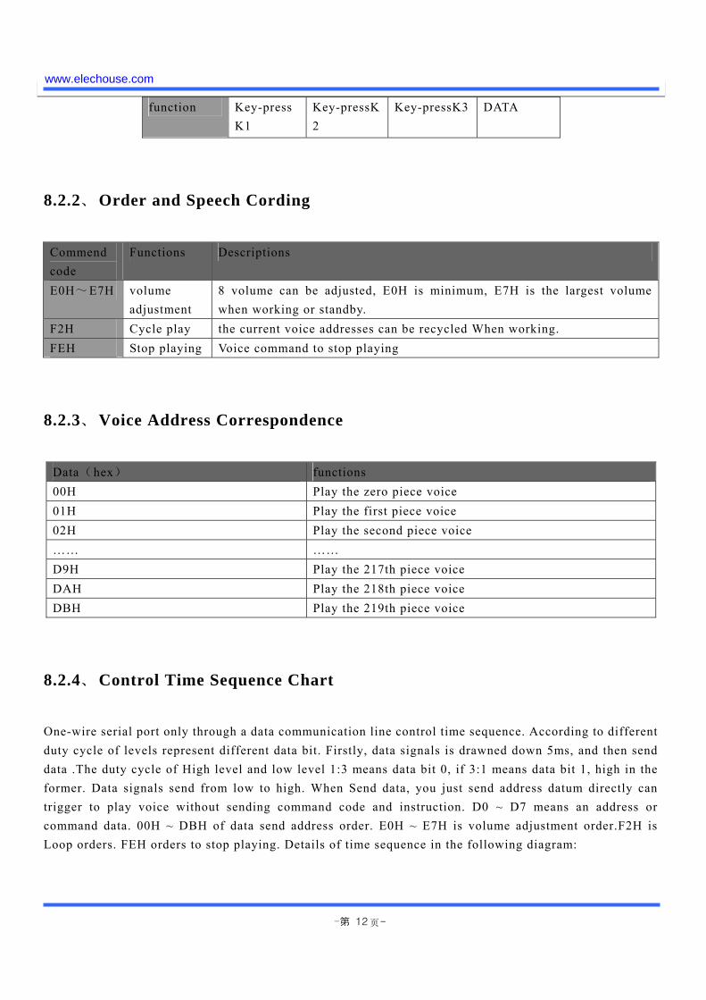
8.2.2、Order and Speech Cording
Commend code
Functions Descriptions
E0H~E7H volume adjustment
8 volume can be adjusted, E0H is minimum, E7H is the largest volume when working or standby.
F2H Cycle play the current voice addresses can be recycled When working. FEH Stop playing Voice command to stop playing
8.2.3、Voice Address Correspondence
Data(hex) functions 00H Play the zero piece voice 01H Play the first piece voice 02H Play the second piece voice …… …… D9H Play the 217th piece voice DAH Play the 218th piece voice DBH Play the 219th piece voice
8.2.4、Control Time Sequence Chart
One-wire serial port only through a data communication line control time sequence. According to different duty cycle of levels represent different data bit. Firstly, data signals is drawned down 5ms, and then send data .The duty cycle of High level and low level 1:3 means data bit 0, if 3:1 means data bit 1, high in the former. Data signals send from low to high. When Send data, you just send address datum directly can trigger to play voice without sending command code and instruction. D0 ~ D7 means an address or command data. 00H ~ DBH of data send address order. E0H ~ E7H is volume adjustment order.F2H is Loop orders. FEH orders to stop playing. Details of time sequence in the following diagram:
www.elechouse.com

页-
-第 13
DATA
VOICE
BUSY
5m s
D0 D1 D2 D3 D4 D5 D6 D7
20m s
Description: WT588D-U can not enter dormant state under the one-wire serial interface. Therefore, using with caution when battery-powered .DATA is a communications line for one-wire serial interface, WT588D-U voice module begins to send data signals after current is switched on and wait 17ms.BUSY voice for the busy signal output. Wait for 20ms Data after sent successfully. And BUSY output will be to respond. Details of data bit duty cycle in the following chart:
High level:Low level=1:3 means 0 High level:Low level =3:1 means 1
8.2.5、The Example of 1-Wire Serial Port Control Time Sequence
For example, Send time sequence of data 9CH chart in one-Wire Serial Port Control mode is show in figure:
DATA
VOICE
BUSY
5m s0 0 1 1 1 0 0 1
20m s
8.2.6、Models of Procedure
Master SCM:PIC16F54,Clock frequency :4MHz Send one-line (unsigned char addr) { sda=0; delay1ms(5); /* Data signals at low level 5ms */ for(i=0;i<8;i++) { sda=1; if(addr & 1)
www.elechouse.com
页-
-第 14
{delay1us(600); /* High level:Low level =600us:200us,means data=1 */ sda=0; delay1us(200);} else{ delay1us(600); /* High level:Low level =200us:600us,means data=0 */ sda=0; delay1us(200); } addr>>=1; } sda=1; }
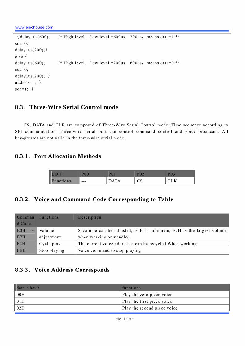
8.3、Three-Wire Serial Control mode
CS, DATA and CLK are composed of Three-Wire Serial Control mode .Time sequence according to SPI communication. Three-wire serial port can control command control and voice broadcast. All key-presses are not valid in the three-wire serial mode.
8.3.1、Port Allocation Methods
I/O 口 P00 P01 P02 P03 Functions --- DATA CS CLK
8.3.2、Voice and Command Code Corresponding to Table
Command Code
Functions Description
E0H ~
E7H Volume adjustment
8 volume can be adjusted, E0H is minimum, E7H is the largest volume when working or standby.
F2H Cycle play The current voice addresses can be recycled When working. FEH Stop playing Voice command to stop playing
8.3.3、Voice Address Corresponds
data(hex) functions 00H Play the zero piece voice 01H Play the first piece voice 02H Play the second piece voice
www.elechouse.com
页-
-第 15
…… …… D9H Play the 217th piece voice DAH Play the 218th piece voice DBH Play the 219th piece voice
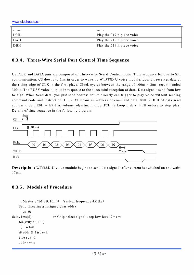
8.3.4、Three-Wire Serial Port Control Time Sequence
CS, CLK and DATA pins are composed of Three-Wire Serial Control mode .Time sequence follows to SPI communication. CS downs to 5ms in order to wake-up WT588D-U voice module. Low bit receives data at the rising edge of CLK in the first place. Clock cycles between the range of 100us ~ 2ms, recommended 300us. The BUSY voice outputs in response to the successful reception of data. Data signals send from low to high. When Send data, you just send address datum directly can trigger to play voice without sending command code and instruction. D0 ~ D7 means an address or command data. 00H ~ DBH of data send address order. E0H ~ E7H is volume adjustment order.F2H is Loop orders. FEH orders to stop play. Details of time sequence in the following diagram:
CS
CLK
DATA
VOICE
BUSY
D0 D1 D2 D3 D4 D5 D6 D7
20m s
5m s
300us
Description: WT588D-U voice module begins to send data signals after current is switched on and wairt 17ms.
8.3.5、Models of Procedure
(Master SCM PIC16F54,System frequency 4MHz) Send threelines(unsigned char addr) {cs=0; delay1ms(5); /* Chip select signal keep low level 2ms */ for(i=0;i<8;i++) { scl=0; if(addr & 1)sda=1; else sda=0; addr>>=1;
www.elechouse.com
页-
-第 16
delay1us(300); /* Clock cycle 300us */ scl=1; delay1us(300); } cs=1;}
9、Typical Application Circuit
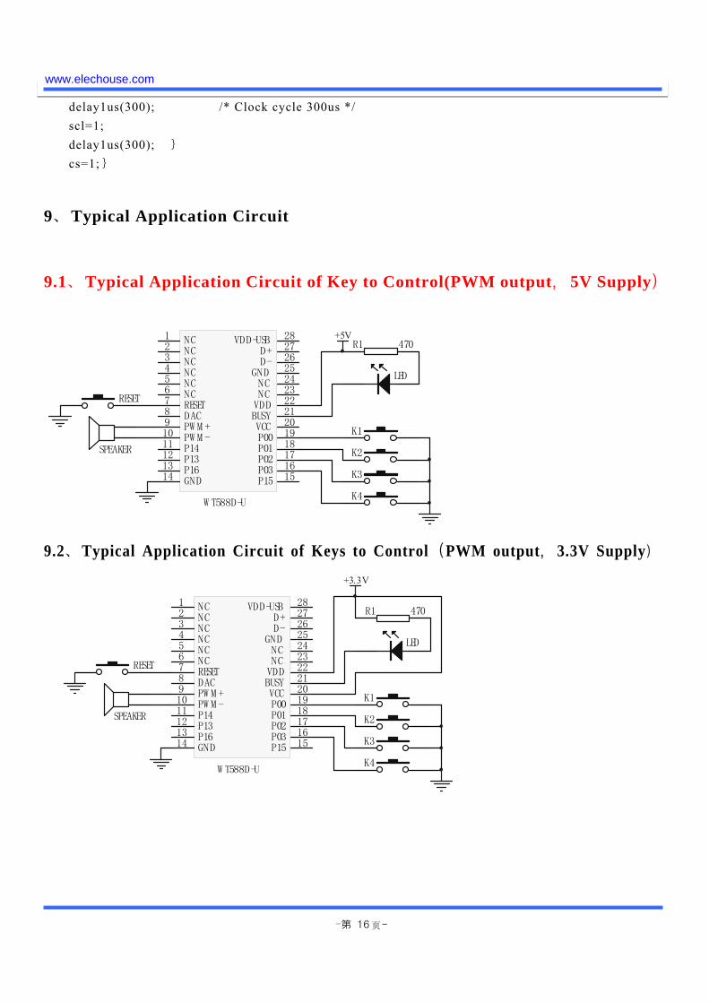
9.1、Typical Application Circuit of Key to Control(PWM output,5V Supply)
1234567891011121314 15
16171819202122232425262728NC
NCNCNCNCNCRESETDACPW M +PW M -P14P13P16GND P15
P03P02P01P00VCCBUSYVDDNCNC
GNDD-D+
VDD-USB
W T588D-U
SPEAKER
+5VR1 470
LED
K1
K2
K3
K4
RESET
9.2、Typical Application Circuit of Keys to Control(PWM output,3.3V Supply)
1234567891011121314 15
16171819202122232425262728NC
NCNCNCNCNCRESETDACPW M +PW M -P14P13P16GND P15
P03P02P01P00VCCBUSYVDDNCNC
GNDD-D+
VDD-USB
W T588D-U
SPEAKER
+3.3V
R1 470
LED
K1
K2
K3
K4
RESET
www.elechouse.com

页-
-第 17
9.3 、 Typical Application Circuit of Keys to Control ( DAC output )
1234567891011121314 15
16171819202122232425262728NC
NCNCNCNCNCRESETDACPW M +PW M -P14P13P16GND P15
P03P02P01P00VCCBUSYVDDNCNC
GNDD-D+
VDD-USB
W T588D-U
D2 4007
D1 4007+5V
R1 470
LED
K1
K2
K3
K4
RESET
C11 250uF
C10
0.05uF
C9
10uF
C7
10uF
R7
10Ω
61
8
5
7
4
3
2
SPEAKER
VCC
LM386
10KΩ
C8 1uF
R2
1.2K
C6
104
Note: DAC output port together with the ground, which connect with a 1.2K resistor and capacitor 104.
when use DAC output way, and then the audio signal re-entering amplifier part, as circuit diagram of R2, R6 shown.
9.4、Typical Application of one-line Serial Control Circuit (PWM out)
1234567891011121314 15
16171819202122232425262728NC
NCNCNCNCNCRESETDACPW M +PW M -P14P13P16GND P15
P03P02P01P00VCCBUSYVDDNCNC
GNDD-D+
VDD-USB
W T588D-U
M CU
+5VR1 470
LED
+5V
SPEAKER
DATA
9.5、Typical Application of First-line Serial Control Circuit(DAC Output)
www.elechouse.com

页-
-第 18
1234567891011121314 15
16171819202122232425262728NC
NCNCNCNCNCRESETDACPW M +PW M -P14P13P16GND P15
P03P02P01P00VCCBUSYVDDNCNC
GNDD-D+
VDD-USB
W T588D-U
M CU
+5VR1 470
LED
+5V
C11 250uF
C10
0.05uF
C9
10uF
C7
10uF
R7
10Ω
61
8
5
7
4
3
2
SPEAKER
VCC
LM386
10KΩ
C8 1uF
R2
1.2K
C6
104 DATA
Note: DAC output port together with the land , which connect with a 1.2K resistor and capacitor 104.
when use DAC output way, and then the audio signal re-entering amplifier part, as circuit diagram of R2, R6 shown.
9.6 、 0ne-Wire Serial Port MCU5V Power/ Module 3.3V Power Supply
Application circuit (PWM output)
1234567891011121314 15
16171819202122232425262728NC
NCNCNCNCNCRESETDACPW M +PW M -P14P13P16GND P15
P03P02P01P00VCCBUSYVDDNCNC
GNDD-D+
VDD-USB
W T588D-U
M CU
+3.3V
R1 470
LED
+5V
SPEAKER DATACSCLKR4
470Ω×3
R3R2
www.elechouse.com
页-
-第 19
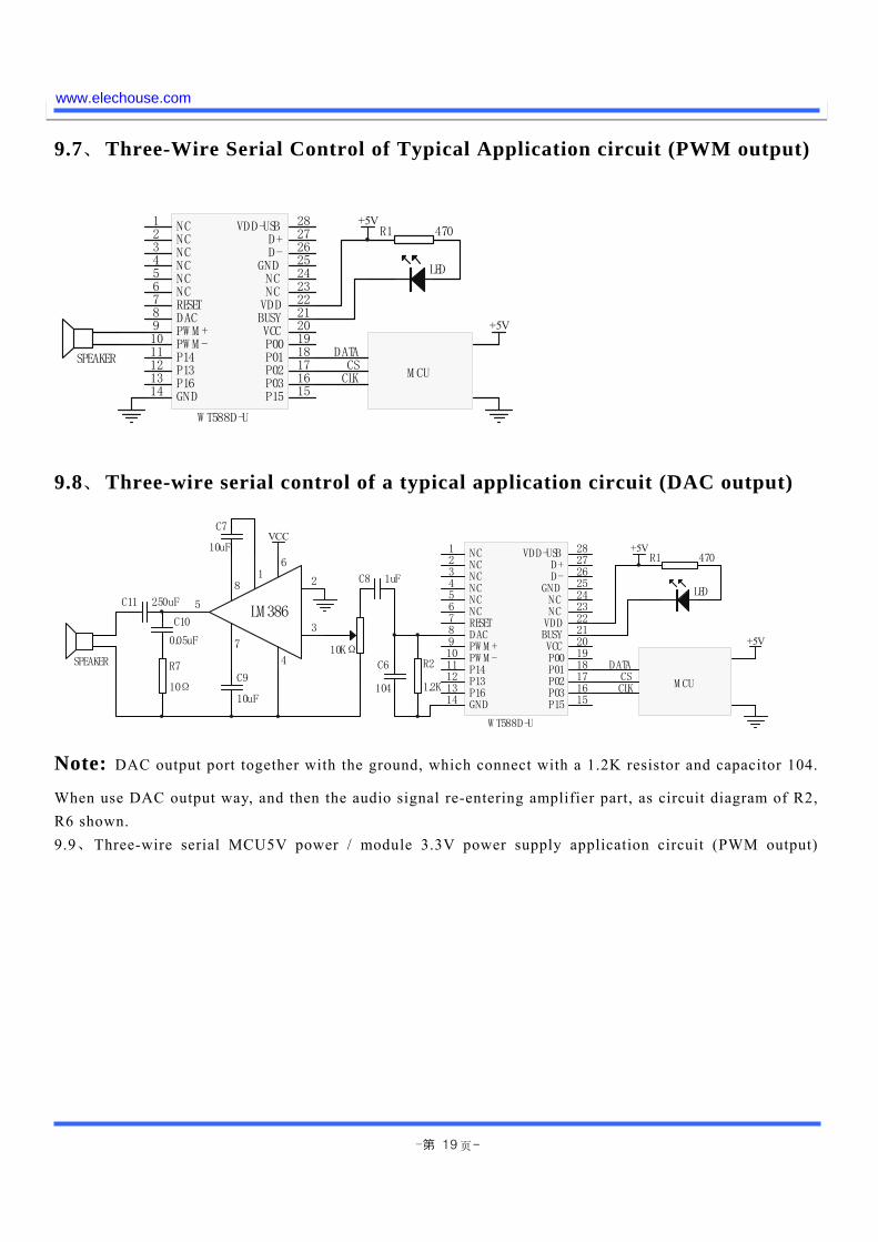
9.7、Three-Wire Serial Control of Typical Application circuit (PWM output)
1234567891011121314 15
16171819202122232425262728NC
NCNCNCNCNCRESETDACPW M +PW M -P14P13P16GND P15
P03P02P01P00VCCBUSYVDDNCNC
GNDD-D+
VDD-USB
W T588D-U
M CU
+5VR1 470
LED
+5V
SPEAKERDATA
CSCLK
9.8、Three-wire serial control of a typical application circuit (DAC output)
1234567891011121314 15
16171819202122232425262728NC
NCNCNCNCNCRESETDACPW M +PW M -P14P13P16GND P15
P03P02P01P00VCCBUSYVDDNCNC
GNDD-D+
VDD-USB
W T588D-U
M CU
+5VR1 470
LED
+5V
C11 250uF
C10
0.05uF
C9
10uF
C7
10uF
R7
10Ω
61
8
5
7
4
3
2
SPEAKER
VCC
LM386
10KΩ
C8 1uF
R2
1.2K
C6
104
DATACSCLK
Note: DAC output port together with the ground, which connect with a 1.2K resistor and capacitor 104.
When use DAC output way, and then the audio signal re-entering amplifier part, as circuit diagram of R2, R6 shown. 9.9、Three-wire serial MCU5V power / module 3.3V power supply application circuit (PWM output)
www.elechouse.com

页-
-第 20
MCU5V
1234567891011121314 15
16171819202122232425262728NC
NCNCNCNCNCRESETDACPW M +PW M -P14P13P16GND P15
P03P02P01P00VCCBUSYVDDNCNC
GNDD-D+
VDD-USB
W T588D-U
M CU
+3.3V
R1 470
LED
+5V
SPEAKER
DATAR2 470
10、Control procedures
10.1、One-wire serial control of assembler
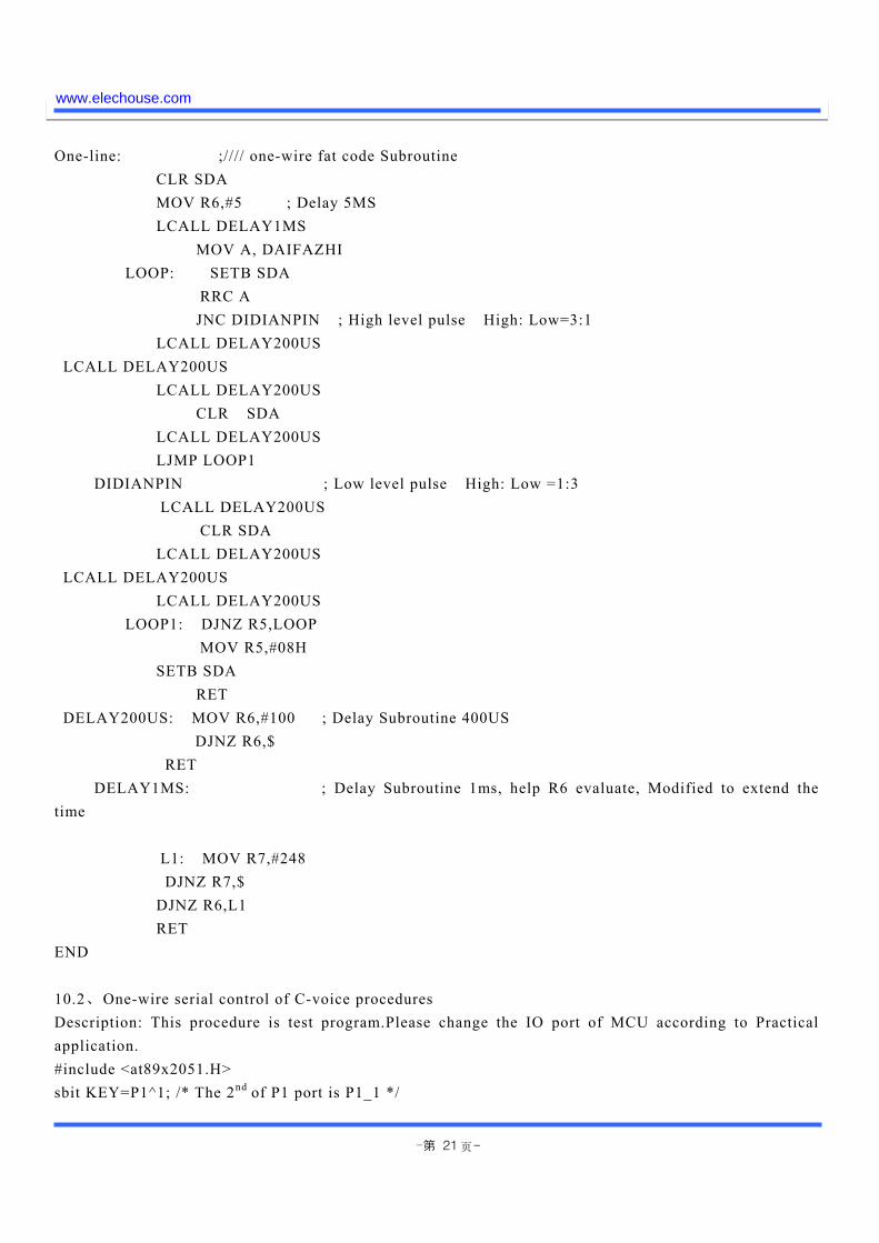
Description: This procedure is test program. Please change the IO port of MCU according to Practical application. ORG 0000H KEY EQU P1.1 ; Button pin SDA EQU P3.0 ; Data pin DAIFAZHI EQU 50H ; A temporary address for Code value MOV DAIFAZHI,#0H; Code made the initial value of 0 MOV R5,#8 ; 8-bit Circulation of Fat Code MAIN: JB KEY,MAIN MOV R6,#20 ;Delay 20MS LCALL DELAY1MS JB KEY,MAIN ; Buffeting button to judgment JNB KEY,$ ;Wait for button release LCALL one-line ; Transfer one-wire fat code Subroutine INC DAIFAZHI ; Code value plus 1 fat MOV A,DAIFAZHI CJNE A,#220,XX2 ;Whether reach max 220 of the Voice paragraph or not XX2: JC XX3 MOV DAIFAZHI,#0H XX3: LJMP MAIN
www.elechouse.com
页-
-第 21
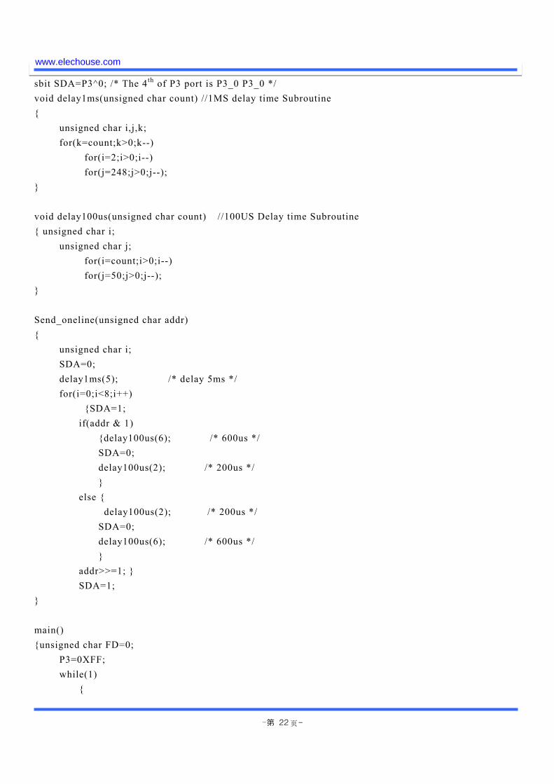
One-line: ;//// one-wire fat code Subroutine CLR SDA MOV R6,#5 ; Delay 5MS LCALL DELAY1MS MOV A, DAIFAZHI LOOP: SETB SDA RRC A JNC DIDIANPIN ; High level pulse High: Low=3:1 LCALL DELAY200US LCALL DELAY200US LCALL DELAY200US CLR SDA LCALL DELAY200US LJMP LOOP1 DIDIANPIN ; Low level pulse High: Low =1:3 LCALL DELAY200US CLR SDA LCALL DELAY200US LCALL DELAY200US LCALL DELAY200US LOOP1: DJNZ R5,LOOP MOV R5,#08H SETB SDA RET DELAY200US: MOV R6,#100 ; Delay Subroutine 400US DJNZ R6,$ RET DELAY1MS: ; Delay Subroutine 1ms, help R6 evaluate, Modified to extend the time L1: MOV R7,#248 DJNZ R7,$ DJNZ R6,L1 RET END 10.2、One-wire serial control of C-voice procedures Description: This procedure is test program.Please change the IO port of MCU according to Practical application. #include <at89x2051.H> sbit KEY=P1^1; /* The 2nd of P1 port is P1_1 */
www.elechouse.com
页-
-第 22
sbit SDA=P3^0; /* The 4th of P3 port is P3_0 P3_0 */ void delay1ms(unsigned char count) //1MS delay time Subroutine unsigned char i,j,k; for(k=count;k>0;k--) for(i=2;i>0;i--) for(j=248;j>0;j--); void delay100us(unsigned char count) //100US Delay time Subroutine unsigned char i; unsigned char j; for(i=count;i>0;i--) for(j=50;j>0;j--); Send_oneline(unsigned char addr) unsigned char i; SDA=0; delay1ms(5); /* delay 5ms */ for(i=0;i<8;i++) SDA=1; if(addr & 1) delay100us(6); /* 600us */ SDA=0; delay100us(2); /* 200us */ else delay100us(2); /* 200us */ SDA=0; delay100us(6); /* 600us */ addr>>=1; SDA=1; main() unsigned char FD=0; P3=0XFF; while(1)
www.elechouse.com

页-
-第 23
if(KEY==0) delay1ms(10); if(KEY==0) // Increase Code value of fat by button P1.1. Send online (FD); FD++; if(FD==220) // 0ne-wire Serial port, the voice segment up to a maximum of 220 FD=0; while(KEY==0); // Waiting for button release in order to avoid Miscarriage of justice
10.3、Three-wire serial control of assembler
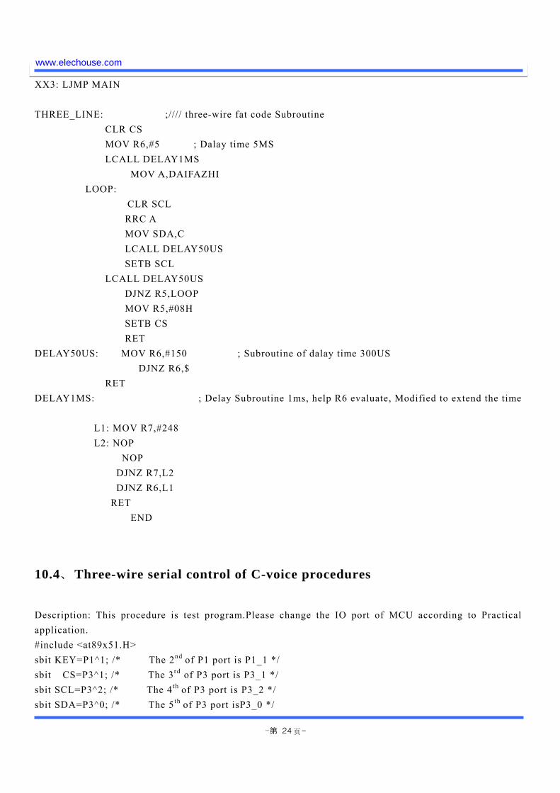
Description: This procedure is test program.Please change the IO port of MCU according to Practical application. ORG 0000H KEY EQU P1.1 ; Button pin CS EQU P3.1 ;CS trigger pin SCL EQU P3.2 ;Clock pin SDA EQU P3.0 ;Data pin DAIFAZHI EQU 50H;A temporary address for Code value MOV DAIFAZHI,#0H;Code made the initial value of 0 MOV R5,#8 ;Code made the initial value of 0 MAIN: JB KEY,MAIN MOV R6,#20 ;Dalay time 20MS LCALL DELAY1MS JB KEY,MAIN ; Buffeting button to judgment JNB KEY,$ ; Wait for button release LCALL THREE_LINE; Transfer three-wire fat code Subroutine INC DAIFAZHI ; Code value plus 1 fat MOV A,DAIFAZHI CJNE A,#220,XX2 ; Whether reach max 220 of the Voice paragraph or not XX2: JC XX3 MOV DAIFAZHI,#0H
www.elechouse.com
页-
-第 24
XX3: LJMP MAIN THREE_LINE: ;//// three-wire fat code Subroutine CLR CS MOV R6,#5 ; Dalay time 5MS LCALL DELAY1MS MOV A,DAIFAZHI LOOP: CLR SCL RRC A MOV SDA,C LCALL DELAY50US SETB SCL LCALL DELAY50US DJNZ R5,LOOP MOV R5,#08H SETB CS RET DELAY50US: MOV R6,#150 ; Subroutine of dalay time 300US DJNZ R6,$ RET DELAY1MS: ; Delay Subroutine 1ms, help R6 evaluate, Modified to extend the time L1: MOV R7,#248 L2: NOP NOP DJNZ R7,L2 DJNZ R6,L1 RET END
10.4、Three-wire serial control of C-voice procedures
Description: This procedure is test program.Please change the IO port of MCU according to Practical application. #include <at89x51.H> sbit KEY=P1^1; /* The 2nd of P1 port is P1_1 */ sbit CS=P3^1; /* The 3rd of P3 port is P3_1 */ sbit SCL=P3^2; /* The 4th of P3 port is P3_2 */ sbit SDA=P3^0; /* The 5th of P3 port isP3_0 */
www.elechouse.com

页-
-第 25
//sbit DENG=P3^7; /* The 6th of P3 port is P3_5- */ void delay1ms(unsigned char count) //1MS Dalay time subroutine unsigned char i,j,k; for(k=count;k>0;k--) for(i=2;i>0;i--) for(j=248;j>0;j--); void delay100us(void) //100US Dalay time subroutine unsigned char j; for(j=50;j>0;j--); Send_threelines(unsigned char addr) // three-wire fat code Subroutine unsigned char i; CS=0; delay1ms(5); for(i=0;i<8;i++) SCL=0; if(addr & 1)SDA=1; else SDA=0; addr>>=1; Delay300us(); /* 300us */ SCL=1; Delay300us(); CS=1; main() unsigned char FD=0; P3=0XFF; while(1) if(KEY==0) delay1ms(20); if(KEY==0) //Increase Code value of fat by button P1.1. Send three-line (FD);
www.elechouse.com

页-
-第 26
FD++; if(FD==220//Three-wire Serial port, the voice segment up to a maximum of 220 FD=0; while(KEY==0); // Waiting for button release in order to avoid Miscarriage of justice
11、Package size Figure
Units:mm
46.80
18.30
12.0732.92
15.23
1.00
2.54
www.elechouse.com