Embed Size (px)
DESCRIPTION
UTB SOI for LER/RDF. EECS Min Hee Cho. Introduction LER (Line Edge Roughness) RDF (Random Dopant Fluctuation) Variation Solution – UTB SOI Results Process of UTB Conclusion. Outline. Introduction. 1m size ball. 3nm. TR (1947). Price : less than 1 Nano dollar for each TR - PowerPoint PPT Presentation
Citation preview
UTB SOI for LER/RDF
EECS
Min Hee Cho
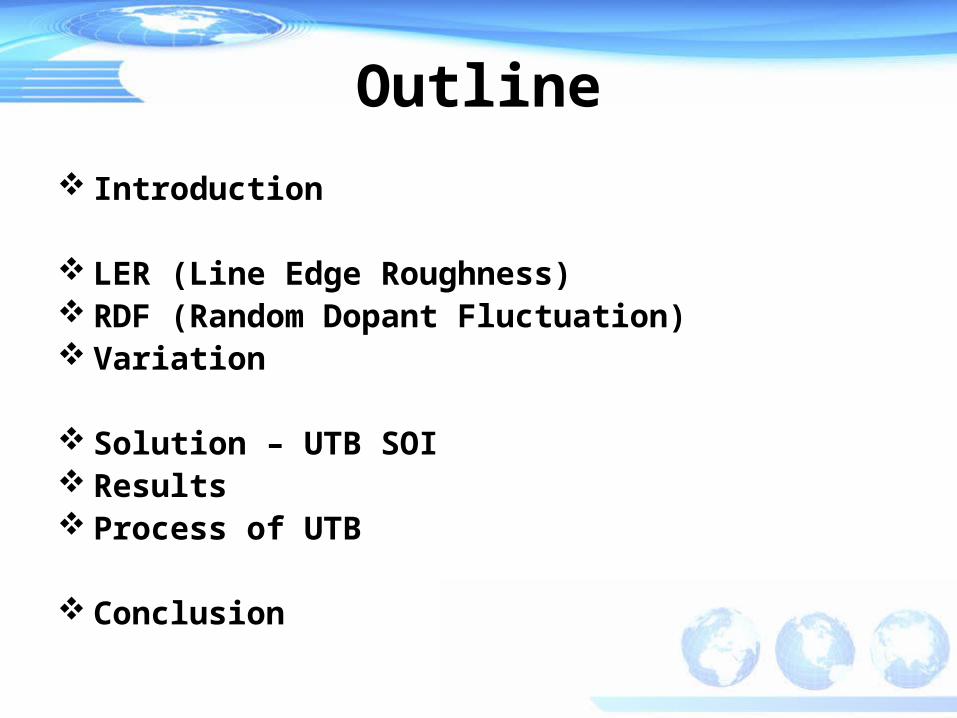
Outline
Introduction
LER (Line Edge Roughness) RDF (Random Dopant Fluctuation) Variation
Solution – UTB SOI Results Process of UTB
Conclusion
Introduction
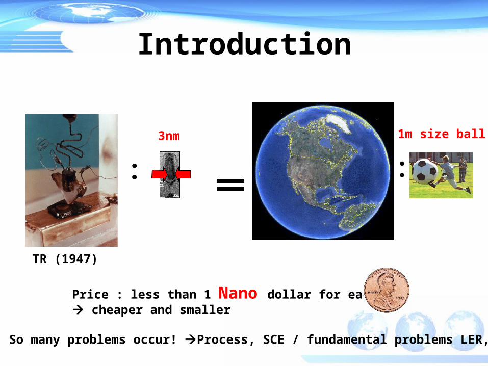
TR (1947)
However, So many problems occur! Process, SCE / fundamental problems LER, RDF etc
3nm
Price : less than 1 Nano dollar for each TR cheaper and smaller
1m size ball
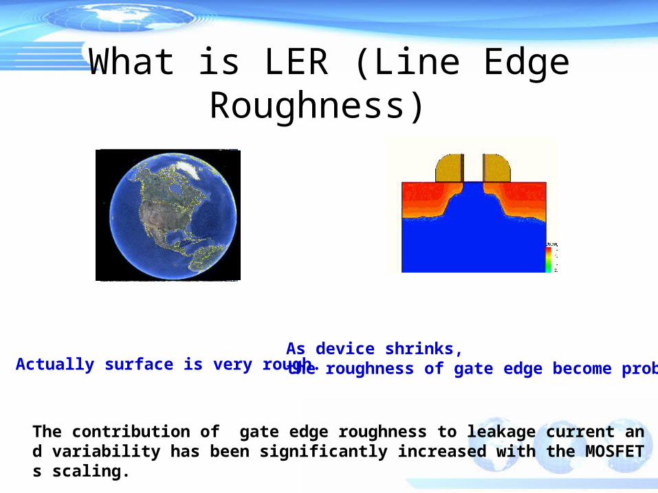
What is LER (Line Edge Roughness)
The contribution of gate edge roughness to leakage current and variability has been significantly increased with the MOSFETs scaling.
Actually surface is very rough.As device shrinks, the roughness of gate edge become problem
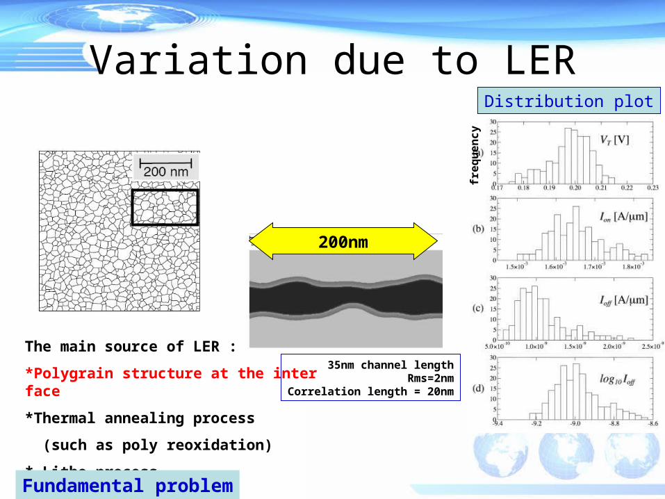
Variation due to LER
The main source of LER :
*Polygrain structure at the interface
*Thermal annealing process
(such as poly reoxidation)
* Litho-process
35nm channel lengthRms=2nm
Correlation length = 20nm
Distribution plot
200nm
Fundamental problemfr
eq
uen
cy
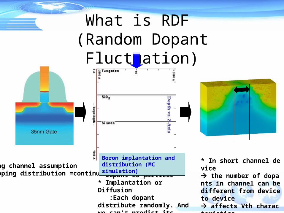
What is RDF (Random Dopant Fluctuation)
* Dopant is particle* Implantation or Diffusion :Each dopant distribute randomly. And we can’t predict its exact place.
*Long channel assumption: Doping distribution =continuous
* In short channel device the number of dopants in channel can be different from device to device affects Vth characteristics
Boron implantation and distribution (MC simulation)
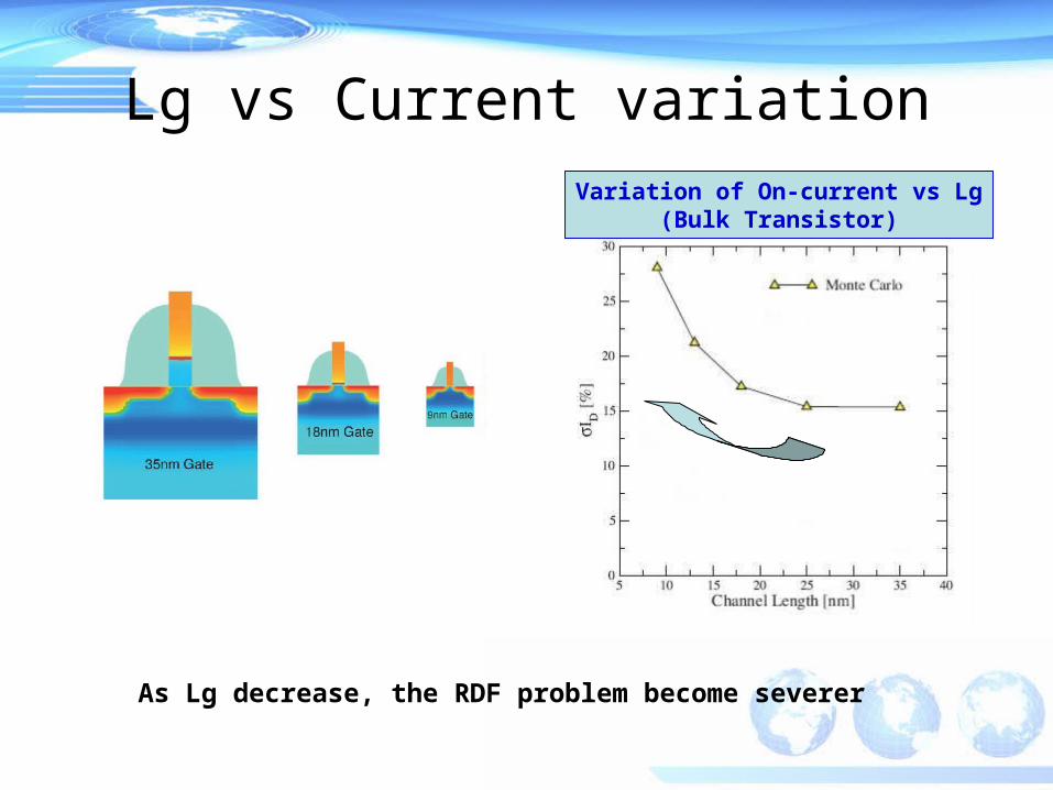
Lg vs Current variation
As Lg decrease, the RDF problem become severer
Variation of On-current vs Lg(Bulk Transistor)
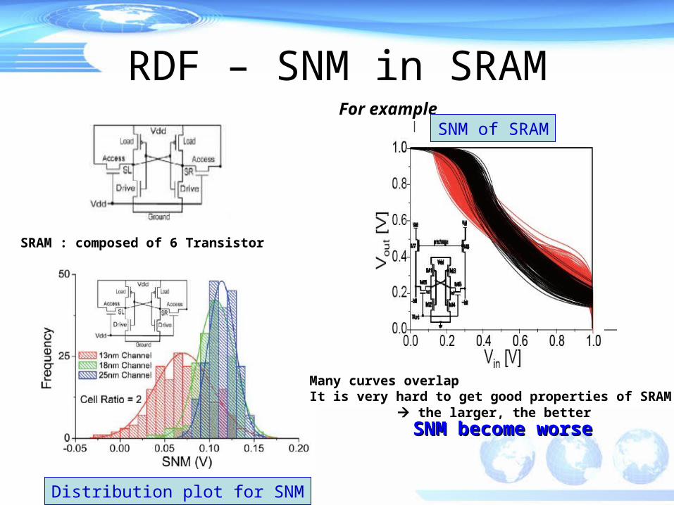
RDF – SNM in SRAM
SRAM : composed of 6 Transistor
Size of square : Static noise margin the larger, the better
For example
SNM- SRAM
Vin
Vou
tMany curves overlapIt is very hard to get good properties of SRAM
SNM become worseSNM become worse
200 cases35nm Lg
Distribution plot for SNM
SNM of SRAM
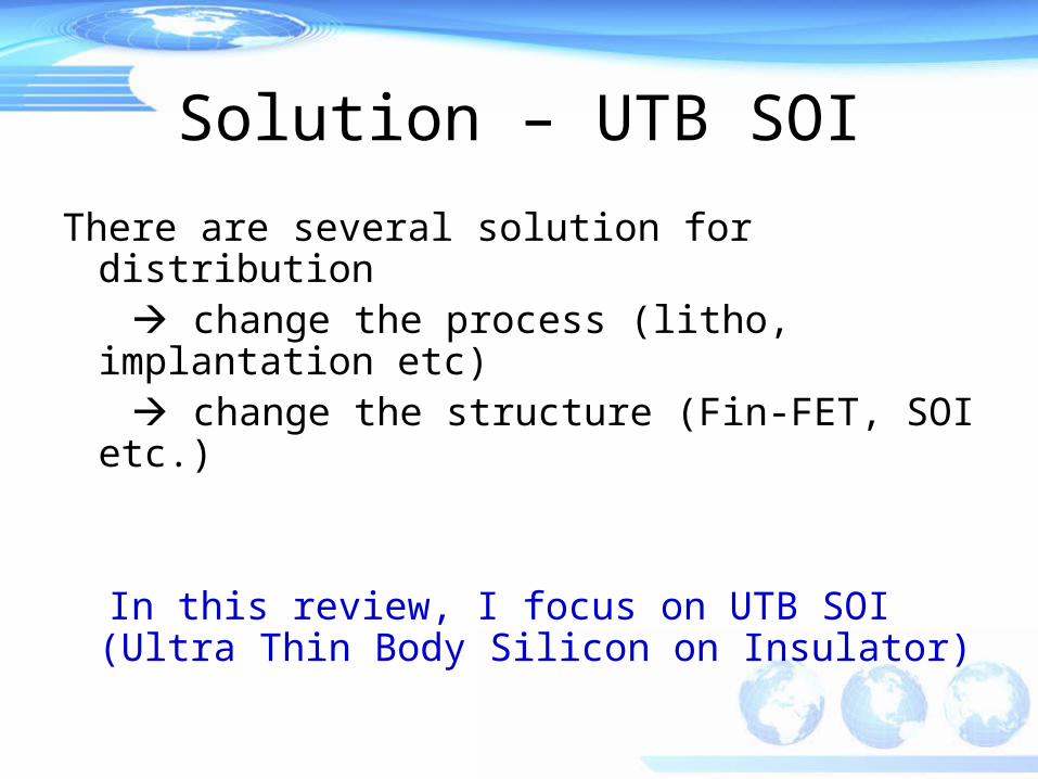
Solution – UTB SOI
There are several solution for distribution change the process (litho, implantation etc) change the structure (Fin-FET, SOI etc.)
In this review, I focus on UTB SOI (Ultra Thin Body Silicon on Insulator)
LDD
BOX (SiO2)
SOI (Si)
Gate
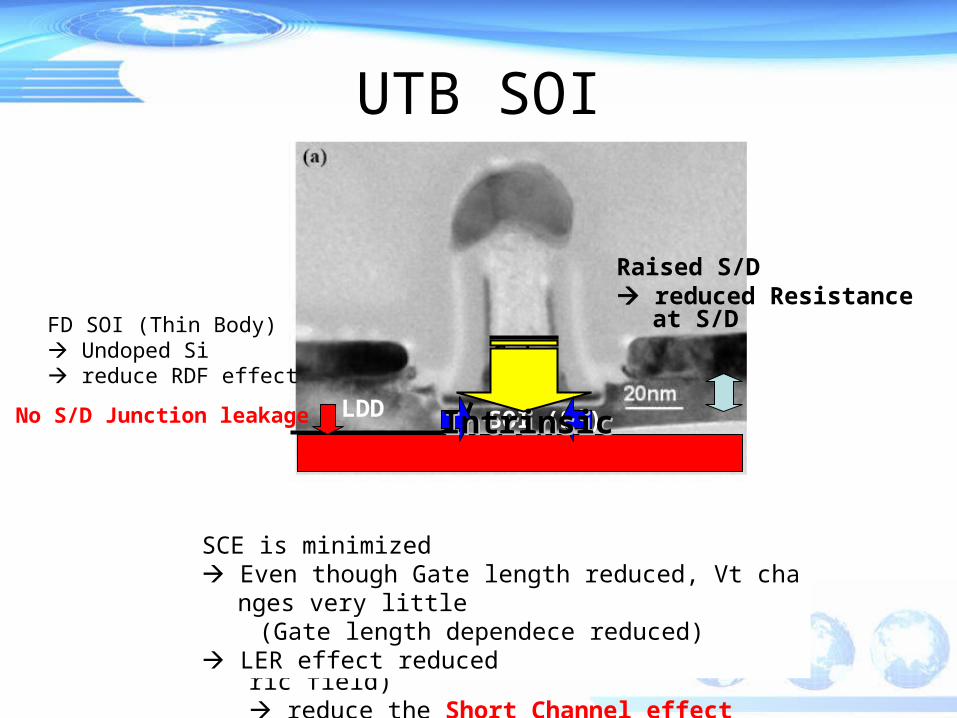
UTB SOI
Raised S/D reduced Resistance at S/D
No S/D Junction leakage
Thin SOI (5~10nm) Fullly Depleted (channel region controlled by only gate tightly) reduce lateral Field (Drain electric field) reduce the Short Channel effect (DIBL)
SCE is minimized Even though Gate length reduced, Vt changes very little (Gate length dependece reduced) LER effect reduced
FD SOI (Thin Body) Undoped Si reduce RDF effect
IntrinsicIntrinsic
Results
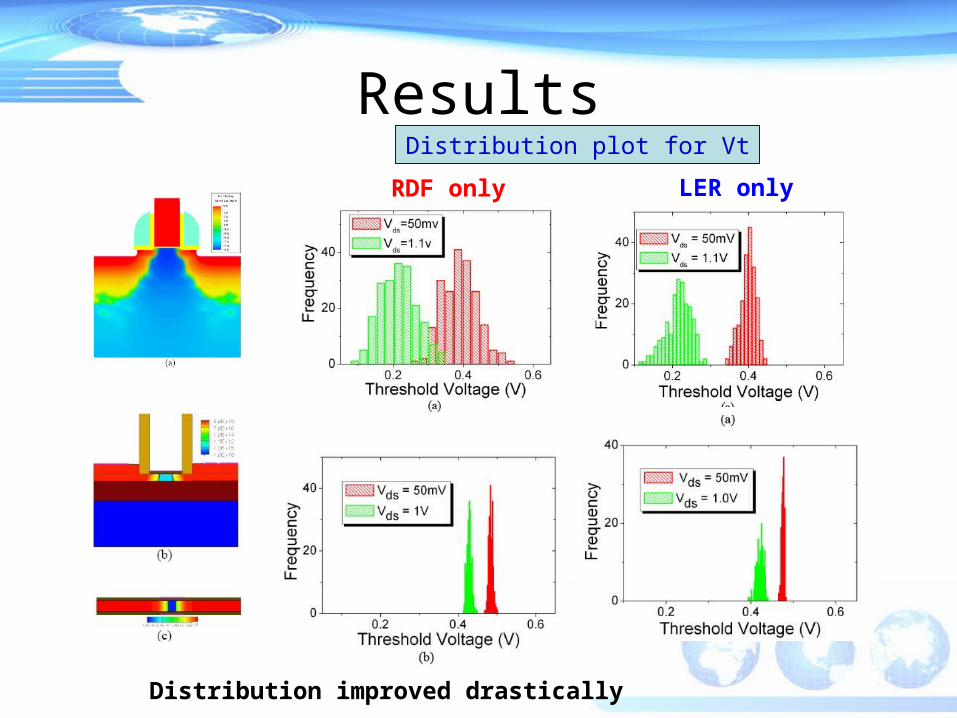
RDF only LER only
Distribution improved drastically
Distribution plot for Vt
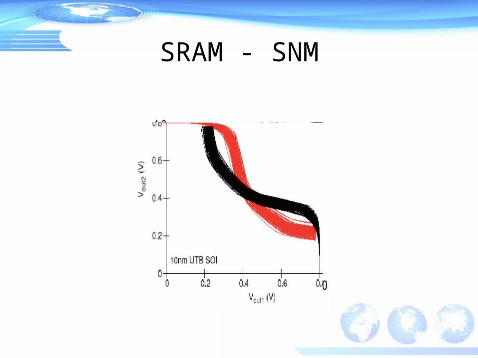
SRAM - SNM
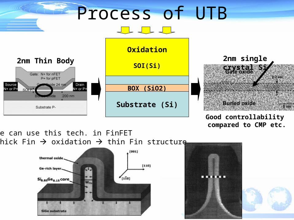
Process of UTB
Substrate (Si)
BOX (SiO2)SOI(Si)
Wet etch
Substrate (Si)
BOX (SiO2)
SOI(Thick Si)
Oxidation
SOI(Si)2nm single crystal Si
Good controllability compared to CMP etc.
We can use this tech. in FinFET: Thick Fin oxidation thin Fin structure
2nm Thin Body
Conclusion
As transistor shrinks, the fundamental problems such as (RDF, LER) become problems
UTB SOI can be one of solutions
UTB SOI : reduce lateral field SCE↓ LER ↓
: FD undoped Si RDF ↓
Review process of UTB SOI
References• “Simulation of Statistical Variability in Nano MOSFETs” Asen Asenov, 2007
VLSI
• “High Immunity to Threshold Voltage Variability in Undoped Ultra-Thin FDSOI MOSFETs and its Physical Understanding” O. Weber et al, 2008 IEDM
• “Evaluation of Intrinsic Parameter Fluctuations on 45, 32 and 22nm Technology Node LP N-MOSFETs” B Cheng et al, Solid-State Device Research Conference, 2008
• “Intrinsic Parameter Fluctuations in Decananometer MOSFETs Introduced by Gate Line Edge Roughness” Asen Asenov et al., TED 2003
• “Impact of SOI Thickness Fluctuation on Threshold Voltage Variation in Ultra-Thin Body SOI MOSFETs” Gen Tsutsui et al, TRANSACTIONS ON NANOTECHNOLOGY 2005
Thank you very much
See you again!
Q&A