Embed Size (px)
Citation preview
UT1553B RTI Remote Terminal Interface
FEATURES
❐ Complete MIL-STD-1553B Remote Terminal interface compliance
❐ Dual-redundant data bus operation supported
❐ Internal illegalization of selected mode code commands
❐ External illegal command definition capability
❐ Automatic DMA control and address generation
❐ Operational status available via dedicated lines or internal status register
❐ ASD/ENASC (formerly SEAFAC) tested and approved
❐ Available in ceramic 84-lead leadless chip carrier and 84-pin pingrid array
❐ Full military operating temperature range, -55°C to +125°C, screened to the specific test methods listed in Table I of MIL-STD-883, Method 5004, Class B
❐ JAN-qualified devices available
Figure 1. UT1553B RTI Functional Block Diagram
MIL
-ST
D-1
553B
SE
RIA
L B
US
TR
AN
SC
EIV
ER
I/O IN
A
OUT
IN
B
OUT
OU
TP
UT
MU
LTIP
LE
XIN
G A
ND
SE
LF
TE
ST
WR
AP
-AR
OU
ND
LO
GIC
DECODERCHANNEL
A
DECODERCHANNEL
B
ENCODER
MUX
16
MODE CODE/SUB ADDRESS
COMMANDRECOGNITION
LOGIC
CONTROLAND
ERROR LOGIC
DATATRANSFER
LOGIC
ILLEGAL COMMAND
MEMORYADDRESSCONTROL
TIMEOUT
CLOCK ANDRESET LOGIC
2MHz
DATA I/O BUS
OUTPUT EN
MEMORYADDRESSOUTPUTS
CONTROLINPUTS
HOSTSYSTEM
ADDRESSINPUTS
CONTROLOUTPUTS
TIMERON
12MHz
RESET
RTI-1

RTI-2
Table of Contents
1.0 ARCHITECTURE AND OPERATION. . . . . . . . . . . . . . . . . . . . . . . . . . . . . . . . . . .3
1.1 Host Interface . . . . . . . . . . . . . . . . . . . . . . . . . . . . . . . . . . . . . . . . . . . . . . . . . . .31.1.1 Direct Memory Access . . . . . . . . . . . . . . . . . . . . . . . . . . . . . . . . . . . . . .31.1.2 Transparent Memory Access . . . . . . . . . . . . . . . . . . . . . . . . . . . . . . . . . .4
1.2 Internal Register Description . . . . . . . . . . . . . . . . . . . . . . . . . . . . . . . . . . . . . . .41.3 Mode Codes and Subaddresses . . . . . . . . . . . . . . . . . . . . . . . . . . . . . . . . . . . . .71.4 MIL-STD-1553B Subaddress and Mode Codes . . . . . . . . . . . . . . . . . . . . . . . .91.5 Remote Terminal Address . . . . . . . . . . . . . . . . . . . . . . . . . . . . . . . . . . . . . . . . .91.6 Internal Self-Test . . . . . . . . . . . . . . . . . . . . . . . . . . . . . . . . . . . . . . . . . . . . . . .101.7 Power-up and Master Reset . . . . . . . . . . . . . . . . . . . . . . . . . . . . . . . . . . . . . . .101.8 Encoder and Decoder . . . . . . . . . . . . . . . . . . . . . . . . . . . . . . . . . . . . . . . . . . . .111.9 Illegal Command Decoding . . . . . . . . . . . . . . . . . . . . . . . . . . . . . . . . . . . . . . .11
2.0 MEMORY MAP EXAMPLE . . . . . . . . . . . . . . . . . . . . . . . . . . . . . . . . . . . . . . . . . . . . . . . . . . 12
3.0 PIN IDENTIFICATION AND DESCRIPTION . . . . . . . . . . . . . . . . . . . . . . . . . . . . . . . . . . . 14
4.0 MAXIMUM AND RECOMMENDED OPERATING CONDITIONS. . . . . . . . . . . . . . . . . 21
5.0 DC ELECTRICAL CHARACTERISTICS . . . . . . . . . . . . . . . . . . . . . . . . . . . . . . . . . . . . . . 22
6.0 AC ELECTRICAL CHARACTERISTICS. . . . . . . . . . . . . . . . . . . . . . . . . . . . . . . . . . . . . . . 23
7.0 PACKAGE OUTLINE DRAWINGS . . . . . . . . . . . . . . . . . . . . . . . . . . . . . . . . . . . . . . . . . . . . 38
1.0 ARCHITECTURE AND OPERATION
The UT1553B RTI is an interface device linking a MIL-STD-1553 serial data bus and a host microprocessor system. The RTI’s MIL-STD-1553B interface includes encoding/decoding logic, error detection, command recognition, memory address control, clock, and reset circuits.
DecodersThe UT1553B RTI contains two separate free-running decoders to insure that all redundancy requirements of MIL-STD-1553B are met. Each decoder receives, decodes, and verifies biphase Manchester II data. Proper frequency and edge skew are also verified.
Command Recognition LogicThe command recognition logic monitors the output of both decoders at all times. Recognition of a valid command causes a reset of present interface activity followed by execution of the command. This procedure meets the requirement for superseding valid commands.
EncoderThe encoder receives serial data from the data transfer logic, converts it to Manchester II form with proper synchronization and parity, and passes it to the output and self-test logic.
Data Transfer LogicThe data transfer logic provides double-buffered 16-bit parallel-to-serial and serial-to-parallel conversion during reception and transmission of data.
Memory Address ControlThe memory address control logic controls the output of the three-state address lines during memory access. In DMA system implementations, the memory address control provides RTI-generated addresses. In a pseudo-dual-port memory configuration, the memory address control logic provides either RTI-generated or host system addressing.
Control and Error LogicThe control and error logic performs the following four major functions:
- Interface control for proper processing of MIL-STD-1553B commands
- Error checking of both MIL-STD-1553B data and RTI operation
- Memory control (DMA or pseudo-dual-port) for proper data transfer
- Operational status and control signal generation
Output Multiplexing and Self-Test LogicThis logic directs the output of the encoder to one of four places:- Channel A outputs - Channel B outputs - Channel A decoders during self-test - Channel B decoders during self-test
Clock and Reset LogicThe UT1553B RTI requires a 12MHz input clock to operate properly. The RTI provides a 2MHz output for the system designer to use. The device provides a hardware reset pin as well as software-generated reset.
Timer Logic The UT1553B RTI has a built-in 730ms timer that is activated when the encoder is about to transmit. The timer is reset upon receipt of a valid command, master reset, or a time-out condition.
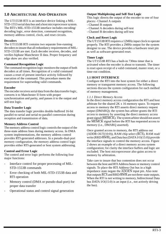
1.1 HOST INTERFACEConfigure the RTI into the host system for either a direct memory or transparent memory access. The following sections discuss the system configuration for each method of memory management.
1.1.1 Direct Memory AccessIn the direct memory access configuration the RTI and host arbitrate for the shared 2K x 16 memory space. To request access to memory the RTI asserts direct memory request output (DMARQ); the system bus arbiter grants the RTI access to memory by asserting the direct memory access grant signal (MEMCK). The system arbiter should not assert the MEMCK signal before the RTI has requested access to memory (i.e., DMARQ asserted).
Once granted access to memory, the RTI address out (ADDR OUT(10:0)), RAM chip select (RCS), RAM read/write (RRD/RWR), and Data bus (DATA I/O(15:0)) provide the interface signals to control the memory access. Figure 2 shows an example of a direct memory access system configuration; for clarity the interface buffers and logic are excluded. The host microprocessor also gains access to memory by arbitration.
Take care to insure that bus contention does not occur between the host and RTI Address buses or memory control signals. To place the RTI Address Out bus in a high impedance state negate the ADOEN input pin. Also note that outputs RCS and RRD/RWR are not three-state outputs. When the RTI is not writing to memory, bidirectional Data bus DATA I/O(15:0) is an input (i.e., not actively driving the bus).
RTI-3
The host microprocessor gains access to the RTI internal registers by controlling input pins CS, CTRL, ADDR IN (10:0), and RD/WR. During message processing the host microprocessor should limit access to RTI internal registers.
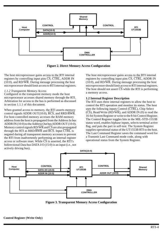
1.1.2 Transparent Memory AccessConfigured in the transparent memory mode the host microprocessor accesses shared memory through the RTI. Arbitration for access to the bus is performed as discussed in section 1.1.1 of this document.
When granted access to memory, the RTI asserts memory control signals ADDR OUT(10:0), RCS, and RRD/RWR. For host-controlled memory accesses the RAM memory address from the host is propagated from the Address In bus ADDR IN (10:0) to the Address Out bus ADDR OUT (10:0). Memory control signals RD/WR and CS are also propagated through the RTI as RRD/RWR and RCS. Input CTRL is negated during all transparent memory accesses to prevent the RTI from inadvertently performing an internal register access or software reset. While CS is asserted, the RTI’s bidirectional Data bus DATA I/O (15:0) is an input (i.e., not actively driving bus).
The host microprocessor gains access to the RTI internal registers by controlling input pins CS, CTRL, ADDR IN (10:0), and RD/WR. During message processing the host microprocessor should limit access to RTI internal registers. The host should not assert CS while the RTI is performing a memory access.
1.2 Internal Register DescriptionThe RTI uses three internal registers to allow the host to control the RTI operation and monitor its status. The host uses the following inputs Control (CTRL), Chip Select (CS), Read/Write (RD/WR), and ADDR IN (0) to read the 16-bit System Register or write to the 8-bit Control Register. The Control Register toggles bits in the MIL-STD-1553B status word, enables biphase inputs, selects terminal active flag, and puts the part in self-test. The System Register supplies operational status of the UT1553B RTI to the host. The Last Command Register saves the command word for a Transmit Last Command mode code, along with operational status from the System Register.
SharedMemory
HostComputer
RTIUT1553B
DMACONTROLLER
Figure 2. Direct Memory Access Configuration
DATA(15:0)
ADDR(10:0)
CONTROL CONTROL
Control Register (Write Only)
Figure 3. Transparent Memory Access Configuration
Shared Memory
HostComputer
RTIUT1553B
DMACONTROLLER
DATA(15:0)
ADDR IN (10:0)
CONTROL
ADDR OUT (10:0)
CONTROL
DATA I/O (15:0)
RTI-4

The 8-bit write-only Control Register manages the operation of the RTI. Write to the Control Register by applying a logic zero to CS, CTRL, RD/WR, and ADDR IN (0); if ADDR IN (0) is a logic one a master reset occurs. Data is loaded into the Control Register via I/O pins DATA(7:0). Control Register writes must occur 50ns before the rising edge of COMSTR to latch data in the outgoing status word.
System Register (Read Only)The 16-bit read-only System Register provides the RTI system status. Read the System Register by applying a logic zero to CS, CTRL, ADDR IN (0), and a logic one to RD/WR. The 16-bit contents of the System Register are read from data I/O pins DATA(15:0).
Bit Number
Initial Condition Description
0 [0] Channel A Enable. A logic one enables Channel A biphase inputs.
1 [0] Channel B Enable. A logic one enables Channel B biphase inputs.
2 [0] Terminal Flag. A logic one sets the Terminal Flag bit of the Status Register.
3 [0] System Busy. A logic one sets the Busy bit of the System Register and inhibits RTI access to memory. No data words are retrieved or stored; command word is stored.
4 [0] Subsystem Busy. A logic one sets the Subsystem Flag bit of the Status Register.
5 [0] Self-Test Channel Select. This bit selects which channel the internal self-test checks; a logic one selects Channel A and a logic zero selects Channel B.
6 [0] Self-Test Enable. A logic one sets the RTI in the internal self-test mode and inhib-its normal operation. Internal testing is not visible on biphase output channels.
7 [0] Service Request. A logic one sets the Service Request bit of the Status Register.
X SRV RQ
SELFTEST
SUBS BUSY TF CH B EN
CH A EN
SELF CH
[ ] defines reset state
CONTROL REGISTER (WRITE ONLY)
MSB
Figure 4. Control Register
X X X X X X X
[0] [0] [0] [0] [0] [0] [0] [0]LSB
Bit Number
Initial Condition Description
0 [0] MCSA(0). The LSB of the mode code or subaddress as indicated by the logic state of bit 5.
1 [0] MCSA(1). Mode code or subaddress as indicated by the state of bit 5.
2 [0] MCSA(2). Mode code or subaddress as indicated by the state of bit 5.
3 [0] MCSA(3). Mode code or subaddress as indicated by the state of bit 5.
4 [0] MCSA(4). Mode code or subaddress as indicated by the state of bit 5.
5 [0] MC/SA. A logic one indicates that bits 4 through 0 are the subaddress of the last command word, and that the last command word was a normal transmit orreceive command. A logic zero indicates that bits 4 through 0 are a mode code, and that the last command was a mode code.
6 [1] Channel A/B. A logic one indicates that the most recent command arrived onChannel A; a logic zero indicates that it arrived on Channel B.
RTI-5

7 [0] Channel B Enabled. A logic one indicates that Channel B is available for both reception and transmission.
8 [0] Channel A Enabled. A logic one indicates that Channel A is available for both reception and transmission.
9 [1] Terminal Flag Enabled. A logic one indicates that the Bus Controller has not issued an Inhibit Terminal Flag mode code. A logic zero indicates that the Bus Controller, via the above mode code, is overriding the host sys-tem’s ability to set the Terminal Flag bit of the status word.
10 [0] Busy. A logic one indicates the Busy bit is set. This bit is reset when the SystemBusy bit in the Control Register is reset.
11 [0] Self-Test. A logic one indicates that the RTI is in the self-test mode. This bit isreset when the self-test is terminated.
12 [0] TA Parity Error. A logic one indicates the wrong Terminal Address parity; it causes the biphase inputs to be disabled and a message error condition. This bit is reset by reloading the terminal address latch with correct parity.
13 [0] Message Error. A logic one indicates that a message error has occurred since the last System Register read. This bit is not reset until the System Register has been examined and the message error condition is removed.
14 [0] Valid Message. A logic one indicates that a valid message has been received since the last System Register read. This bit is not reset until the System Register has been examined.
15 [0] Terminal Active. A logic one indicates the device is executing a transmit or receive operation. The state of this bit is the logical NAND of the external XMIT and RCV pins.
MCSA 4
MCSA 3
TAPA ERR
MESS ERR
VALMESS
MCSA 0
MCSA 1
MCSA 2
SELF-TEST
TERMACTV
BUSY TFEN CH A EN
CH B EN
CHNL A/B
MC/SA
Figure 5. System Registers
[0][0][0][0][0][0][1][0][0][1][0][0][0][0][0][0]
[ ] defines reset state
SYSTEM REGISTER (READ ONLY)
MSB LSB
RTI-6

Last Command Register (Read Only)The 16-bit read-only Last Command Register provides the host with last command and operational status information. The RTI transmits the lower 11 bits of this register along with terminal address upon receipt of a Transmit Last Command mode code. Read the Last Command Register by applying a logic zero to CS, CTRL, and a logic one to RD/WR and ADDR IN (0). The 16-bit contents of the Last Command Register are read from data I/O pins DATA(15:0).
1.3 Mode Codes and SubaddressesThe UT1553B RTI provides subaddress and mode code decoding meeting MIL-STD-1553B. In addition, the device has automatic internal illegal command decoding for reserved MIL-STD-1553B mode codes. Upon command word validation and decode, status pins MCSA(4:0) and MC/SA become valid. Status pin MC/SA will indicate whether the data pins MCSA(4:0) are mode code or subaddress information. Status Register bits 5 through 0 contain the same information as pins MCSA(4:0) and MC/SA.
The system designer can use signals MCSA(4:0), MC/SA, BRDCST, XMIT, and RCV to illegalize mode codes, subaddresses, and other message formats via the Illegal Command (ILL COMM) input (see figure 23 onpage 36).
The RTI will internally decode the following mode codes as illegal:
- Dynamic Bus Control
- Selected Transmitter Shutdown
- Override Selected Transmitter Shutdown
- All Reserved Mode Codes
If the RTI receives one of the above mode codes, the RTI responds by transmitting a status word with the Message Error bit set to logic one.
Mode codes which involve data transfer are processed like receive and transmit commands. The RTI will not generate DMA request for Transmit Status Word and Transmit Last Command mode codes since the information is stored internal to the RTI.
The following mode codes require assistance from the host:
- Synchronize
- Initiate Self-Test
- Reset Remote Terminal
For example, the RTI will accept and respond to a Reset Remote Terminal mode code; however it will not perform a reset operation. The host must interpret the mode code and take appropriate action.
The RTI does not define or interpret the following data words associated with mode code commands:
- Transmit Vector Word
- Synchronize With Data Word
- Transmit Bit Word
The RTI will accept and respond to mode code with data; the host must interpret or define the data word. The RTI will store or retrieve the data required for mode code command from block #1 of the receive or transmit page
.
Bit Number
Initial Condition Description
0 through 10 [all 1s] Least significant 11 bits of the last command word.
11 [0] Busy Bit. System Register bit 10.
12 [0] Self-test. System Register bit 11.
13 [1] Terminal Flag Enabled. System Register bit 9.
14 [1] Channel A/B. System Register bit 6.
15 [1] Illegal Command. The RTI illegalized the last command.
RTI-7
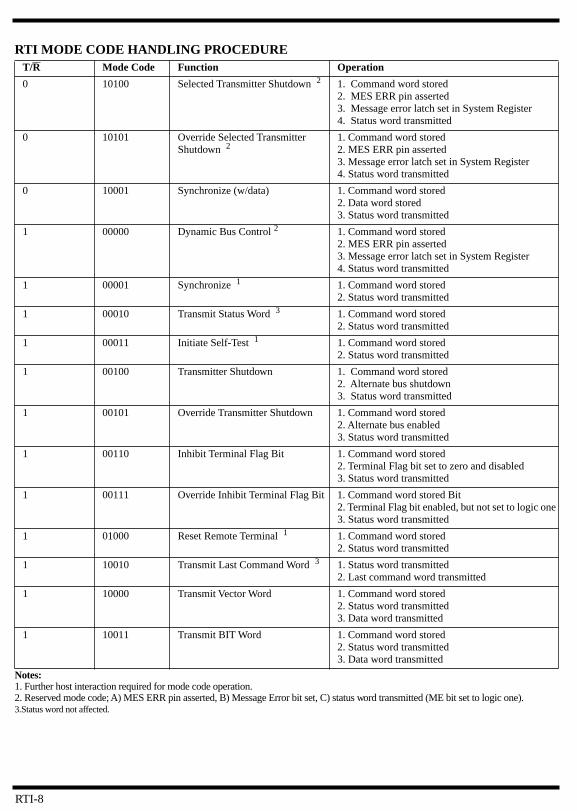
RTI MODE CODE HANDLING PROCEDURET/R Mode Code Function Operation
0 10100 Selected Transmitter Shutdown 2 1. Command word stored 2. MES ERR pin asserted 3. Message error latch set in System Register 4. Status word transmitted
0 10101 Override Selected Transmitter Shutdown 2
1. Command word stored 2. MES ERR pin asserted 3. Message error latch set in System Register 4. Status word transmitted
0 10001 Synchronize (w/data) 1. Command word stored 2. Data word stored 3. Status word transmitted
1 00000 Dynamic Bus Control 2 1. Command word stored 2. MES ERR pin asserted 3. Message error latch set in System Register 4. Status word transmitted
1 00001 Synchronize 1 1. Command word stored 2. Status word transmitted
1 00010 Transmit Status Word 3 1. Command word stored 2. Status word transmitted
1 00011 Initiate Self-Test 1 1. Command word stored 2. Status word transmitted
1 00100 Transmitter Shutdown 1. Command word stored 2. Alternate bus shutdown 3. Status word transmitted
1 00101 Override Transmitter Shutdown 1. Command word stored 2. Alternate bus enabled 3. Status word transmitted
1 00110 Inhibit Terminal Flag Bit 1. Command word stored 2. Terminal Flag bit set to zero and disabled3. Status word transmitted
1 00111 Override Inhibit Terminal Flag Bit 1. Command word stored Bit 2. Terminal Flag bit enabled, but not set to logic one 3. Status word transmitted
1 01000 Reset Remote Terminal 1 1. Command word stored 2. Status word transmitted
1 10010 Transmit Last Command Word 3 1. Status word transmitted 2. Last command word transmitted
1 10000 Transmit Vector Word 1. Command word stored 2. Status word transmitted 3. Data word transmitted
1 10011 Transmit BIT Word 1. Command word stored 2. Status word transmitted 3. Data word transmitted
Notes:1. Further host interaction required for mode code operation. 2. Reserved mode code; A) MES ERR pin asserted, B) Message Error bit set, C) status word transmitted (ME bit set to logic one).3.Status word not affected.
RTI-8

1.4 MIL-STD-1553B Subaddress and Mode Code Definitions
1.5 Remote Terminal AddressAssign the RTI remote terminal address by either a software or hardware exercise. The host assigns the RTI remote terminal address by performing a Control Register write; the Terminal Address bus (TA(4:0)) is strobed into the RTI Remote Terminal Address Register upon completion of the Control Register write. To assign the RTI remote terminal address via hardware, use the TALEN/PARITY input pin operating in the terminal latch address enable mode. The Terminal Address bus is latched into the RTI while the TALEN is asserted (i.e., logic low). Valid remote terminal addresses (RTA) include decimal 0 through 31 if Broadcast is disabled, 0 through 30 if Broadcast is enabled
Parity CheckerAn address parity check is performed to insure the remote terminal address applied to TA(4:0) was properly latched into the Remote Terminal Address Register. To perform a parity check, enable the RTI parity circuit via EXT TEST and EXT TST CH SEL A/B input pins. The parity bit is entered through the TALEN/PARITY input pin operating in the parity mode. Input pins EXT TEST and EXT TST CH SEL A/B control dual-function input pin TALEN/PARITY; see table 2 for description of operation.
If a parity error exists, the Parity Error bit of the System Register is set to a logic one, biphase Channels A and B are disabled (set to logic zero), the Message Error bit set to logic one, and the message error pin is asserted.
Table 1. Subaddress and Mode Code Definitions Per MIL-STD-1553B
Subaddress Field Binary (Decimal)
Message Format
Receive Transmit Description
00000 (00) 1 1 Mode Code Indicator00001 (01) User Defined User Defined00010 (02) User Defined User Defined 00011 (03) User Defined User Defined 00100 (04) User Defined User Defined 00101 (05) User Defined User Defined 00110 (06) User Defined User Defined 00111 (07) User Defined User Defined 01000 (08) User Defined User Defined 01001 (09) User Defined User Defined 01010 (10) User Defined User Defined 01011 (11) User Defined User Defined 01100 (12) User Defined User Defined 01101 (13) User Defined User Defined 01110 (14) User Defined User Defined 01111 (15) User Defined User Defined 10000 (16) User Defined User Defined 10001 (17) User Defined User Defined 10010 (18) User Defined User Defined 10011 (19) User Defined User Defined 10100 (20) User Defined User Defined 10101 (21) User Defined User Defined 10110 (22) User Defined User Defined 10111 (23) User Defined User Defined 11000 (24) User Defined User Defined 11001 (25) User Defined User Defined 11010 (26) User Defined User Defined 11011 (27) User Defined User Defined 11100 (28) User Defined User Defined 11101 (29) User Defined User Defined 11110 (30) User Defined User Defined 11111 (31) 1 1 Mode Code Indicator
Note:1. Refer to mode code assignments per MIL-STD-1553B
RTI-9

The following are examples of sequences used to enter remote terminal addresses into the RTI.
Example 1. Hardware-Controlled Remote Terminal Address (parity check disabled):
STATE 0, 2, or 3 (i.e., 00, 10, or 11) TALEN - asserted (i.e., logic low) TA(4:0) - valid RTA
Example 2. Software-Controlled Remote Terminal Address (parity check disabled):
EXT TEST and EXT TST CH SEL A/B in STATE 0, 2, or 3 (i.e., 00, 10, or 11) CTRL - logic zero CS - logic zero RD/WR - logic zero ADDR IN (0) - logic zeroTALEN - logic one TA(4:0) - valid RTA
Example 3. Software Controlled Remote Terminal Address (parity check enabled):
EXT TEST and EXT TST CH SEL A/B in STATE 1 (i.e., 01) CTRL - logic zero CS - logic zero RD/WR - logic zero ADDR IN (0) - logic zero PARITY - input must provide odd parity for the TA(4:0) bus TA(4:0) - valid RTA
For examples 1 and 2, enabling the parity check circuit (STATE 1) after the remote terminal address is stored results in a parity check of the data loaded into the Remote Terminal Address Register.
1.6 Internal Self-TestSetting bit 6 of the Control Register to a logic one enables the internal self-test. Disable Channels A and B at this time to prevent bus activity during self-test by setting bits 0 and 1 of the Control Register to a logic zero. Normal operation is inhibited when internal self-test is enabled. The RTI’s self-test capability is based on the fact that the MIL-STD-1553B status word sync pulse is identical to the command word sync pulse. Thus, if the status word from the encoder is fed back to the decoder, the RTI will recognize the incoming status word as a command word and thus cause the RTI to transmit another status word. After the host invokes self-test, the RTI self-test logic forces a status word transmission even though the RTI has not received a command word. The status word is sent to decoder A or B depending on the channel the host selected for self-test. The host controls the self-test by periodically changing the bit patterns in the status word being transmitted. Writing to the Control Register bits 2, 3, 4, and 8 changes the status word. Monitor the self-test by sampling either the System Register or the external status pins (i.e. Command Strobe (COMSTR), Transmit (XMIT), Receive (RCV)). For a more detailed explanation of internal self-test, consult the UTMC publication RTI Internal Self-Test Routine.
1.7 Power-up Master ResetReset the RTI by invoking either a hardware or software master reset after power-up to place the device in a known state. The master reset clears the decoder and encoder registers, the command recognition logic, the control and error logic (which includes the Status, Control and System Registers), the data transfer logic, and the memory address control logic. After reset, configure the device for operation via a Control Register write.
Table 2. Parity CheckingSTATE # EXT TEST EXT TST CH SEL A/B Function of TALEN/PARITY
0 0 0 Terminal Address Latch Enable. Active low signal used to latch TA(4:0) into RTI. Internal parity checker disabled.
1 0 1 Parity. Internal remote terminal address parity checker enabled. TALEN/PARITY pin func-tions as parity bit for TA(4:0) bus. Proper oper-ation requires odd parity.
2 1 0 Terminal Address Latch Enable. Do not assert EXT TST during reset, otherwise self-test is invoked.
3 1 1 Terminal Address Latch Enable. Do not assert EXT TST during reset, otherwise self-test is invoked.
RTI-10
Perform a hardware reset by asserting the MRST input pin for a minimum of 500ns. During reset negate the EXT TEST pin (i.e., logic low); assertion of the EXT TEST pin forces the RTI to enter the external self-test mode of operation.
Software reset the RTI by simultaneously applying a logic zero to input pins CS, RD/WR, and CTRL while the least significant bit of the address input bus is a logic one (ADDR IN (0)=0).
1.8 Encoder and DecoderThe RTI interfaces directly to a bus transmitter/receiver via the RTI Manchester II encoder/decoder. The UT1553B RTI receives the command word from the MIL-STD-1553B bus and processes it either by the primary or secondary decoder. Each decode checks for the proper sync pulse and Manchester waveform, edge skew, correct number of bits, and parity. If the command is a receive command, the RTI processes each incoming data word for correct word count and contiguous data. If an invalid message error is detected, the message error pin is asserted, the RTI ceases processing the remainder (if any) of the message, and it then suppresses status word transmission. Upon command validation recognition, the external status outputs are enabled. Reception of illegal commands does not suppress status word transmission.
A timer precludes transmission greater than 730ms by the assertion of fail-safe timer (TIMERON). This timer is reset upon receipt of another valid command.
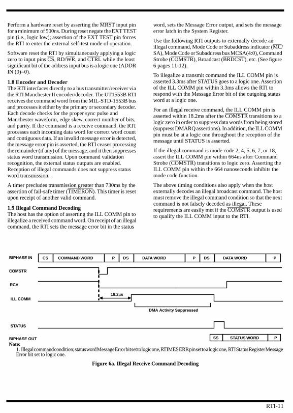
1.9 Illegal Command DecodingThe host has the option of asserting the ILL COMM pin to illegalize a received command word. On receipt of an illegal command, the RTI sets the message error bit in the status
word, sets the Message Error output, and sets the message error latch in the System Register.
Use the following RTI outputs to externally decode an illegal command, Mode Code or Subaddress indicator (MC/SA), Mode Code or Subaddress bus MCSA(4:0), Command Strobe (COMSTR), Broadcast (BRDCST), etc. (See figure 6 pages 11-12).
To illegalize a transmit command the ILL COMM pin is asserted 3.3ms after STATUS goes to a logic one. Assertion of the ILL COMM pin within 3.3ms allows the RTI to respond with the Message Error bit of the outgoing status word at a logic one.
For an illegal receive command, the ILL COMM pin is asserted within 18.2ms after the COMSTR transitions to a logic zero in order to suppress data words from being stored (suppress DMARQ assertions). In addition, the ILL COMM pin must be at a logic one throughout the reception of the message until STATUS is asserted.
If the illegal command is mode code 2, 4, 5, 6, 7, or 18, assert the ILL COMM pin within 664ns after Command Strobe (COMSTR) transitions to logic zero. Asserting the ILL COMM pin within the 664 nanoseconds inhibits the mode code function.
The above timing conditions also apply when the host externally decodes an illegal broadcast command. The host must remove the illegal command condition so that the next command is not falsely decoded as illegal. These requirements are easily met if the COMSTR output is used to qualify the ILL COMM input to the RTI.
PCOMMAND WORDCS DS DATA WORD P
PSTATUS WORDSS
DS DATA WORD PBIPHASE IN
BIPHASE OUT
RCV
COMSTR
STATUS
Figure 6a. Illegal Receive Command Decoding
ILL COMM18.2µs
Note: 1. Illegal command condition; status word Message Error bit set to logic one, RTIMES ERR pin set to a logic one, RTI Status Register Message Error bit set to logic one.
DMA Activity Suppressed
RTI-11

2.0 MEMORY MAP EXAMPLE
The RTI is capable of addressing 2048 x 16 of external memory for message storage. The 2K memory space is divided into two 1K pages and subdivided into 32 blocks of 32 x 16:
Page 1 (Receive): 32 blocks for receive messages (32 x 16)
Page 2 (Transmit): 32 blocks for transmit messages (32 x 16)
Address DecodeThe RTI derives addresses (i.e., data pointers) for external memory directly from the 11 least significant bits of the command word. The address data pointer corresponds to ADDR OUT (10:0) during RTI memory accesses.
T/R = ADDR OUT (10) SUBADDRESS/MODE = ADDR OUT (9:5) WORDCOUNT/MODE CODE = ADDR OUT (4:0)
The T/R bit of the command word becomes the most significant bit of the data pointer; the T/R bit serves to divide the RAM into transmit and receive pages of 1K each. The 5-bit subaddress/mode field is used to select 1 of 32 possible message storage blocks within the transmit or receive message page. The 5-bit word count/mode code field acts as a data pointer to select one of 32 locations within the message storage block. Multiple word messages are stored from top to bottom within the message storage block.
For mode commands, the address data pointer always contains 00000 in the MC/SA field, regardless of whether 00000 or 11111 was received. Forcing the mode code field to 00000 reserves the first message storage block on both pages (receive and transmit) for mode code messages that require data. The 5-bit mode code specifies which of the 32 locations within the message storage block to access.
PCOMMAND WORDCS
PSTATUS WORDSS
BIPHASE IN
BIPHASE OUT
XMIT
STATUS
Figure 6b. Illegal Transmit Command Decoding
ILL COMM
3.3µs
Note: 1. Illegal command condition; status word Message Error bit set to logic one, RTI MES ERR pin set to a logic one, RTI Status Register
Message Error bit set to logic one.
DMA Activity Suppressed
1.0µs (min)
COMSTR
PCSBIPHASE IN
MC/SA
COMSTR
Figure 6c. Mode Code Command Decoding
ILL COMM
664ns
Note: 1. To illegalize mode codes 2, 4, 5, 6, 7, or 18 assert ILL COMM within 664ns of COMSTR’s transition to logic zero. Asserting
the ILL COMM within 664ns inhibits the mode code function.
COMMAND WORD
RTI-12

For “wrap-around” applications (transmission of data previously received), force the RTI to store and receive messages on one memory page. To accomplish one-page
operation do not use the T/R output pin. Eliminating the T/R limits the RTI access to only one page and the RTI will not differentiate between receive and transmit pages.
Table 3. RTI Memory Map
1: Receive Memory Map 2: Transmit Memory map
Block # Operation Address Field (hex) Block # Operation Address Field (hex)
1 Mode Code 1 000 to 01F 1 Mode Code 1 400 to 41F 2 Subaddress 1 020 to 03F 2 Subaddress 1 420 to 43F
3 Subaddress 2 040 to 05F 3 Subaddress 2 440 to 45F
4 Subaddress 3 060 to 07F 4 Subaddress 3 460 to 47F
5 Subaddress 4 080 to 09F 5 Subaddress 4 480 to 49F
6 Subaddress 5 0A0 to 0BF 6 Subaddress 5 4A0 to 4BF
7 Subaddress 6 0C0 to 0DF 7 Subaddress 6 4C0 to 4DF
8 Subaddress 7 0E0 to 0FF 8 Subaddress 7 4E0 to 4FF
9 Subaddress 8 100 to 11F 9 Subaddress 8 500 to 51F
10 Subaddress 9 120 to 13F 10 Subaddress 9 520 to 53F
11 Subaddress 10 140 to 15F 11 Subaddress 10 540 to 55F
12 Subaddress 11 160 to 17F 12 Subaddress 11 560 to 57F
13 Subaddress 12 180 to 19F 13 Subaddress 12 580 to 59F
14 Subaddress 13 1A0 to 1BF 14 Subaddress 13 5A0 to 5BF
15 Subaddress 14 1C0 to 1DF 15 Subaddress 14 5C0 to 5DF
16 Subaddress 15 1E0 to 1FF 16 Subaddress 15 5E0 to 5FF
17 Subaddress 16 200 to 21F 17 Subaddress 16 600 to 61F
18 Subaddress 17 220 to 23F 18 Subaddress 17 620 to 63F
19 Subaddress 18 240 to 25F 19 Subaddress 18 640 to 65F
20 Subaddress 19 260 to 27F 20 Subaddress 19 660 to 67F
21 Subaddress 20 280 to 29F 21 Subaddress 20 680 to 69F
22 Subaddress 21 2A0 to 2BF 22 Subaddress 21 6A0 to 6BF
23 Subaddress 22 2C0 to 2DF 23 Subaddress 22 6C0 to 6DF
24 Subaddress 23 2E0 to 2FF 24 Subaddress 23 6E0 to 6FF
25 Subaddress 24 300 to 31F 25 Subaddress 24 700 to 71F
26 Subaddress 25 320 to 33F 26 Subaddress 25 720 to 73F
27 Subaddress 26 340 to 35F 27 Subaddress 26 740 to 75F
28 Subaddress 27 360 to 37F 28 Subaddress 27 760 to 77F
29 Subaddress 28 380 to 39F 29 Subaddress 28 780 to 79F
30 Subaddress 29 3A0 to 3BF 30 Subaddress 29 7A0 to 7BF
31 Subaddress 30 3C0 to 3DF 31 Subaddress 30 7C0 to 7DF
32 Unused 3E0 to 3FF 32 Unused 7E0 to 7FF
Notes:1. Receive mode codes with data:
- Synchronize with data - Selected Transmitter Shutdown (Illegal) - Override Selected Transmitter Shutdown (Illegal)
2. Transmit mode codes with data:- Transmit Vector Word- Transmit Bit Word
RTI-13

3.0 PIN IDENTIFICATION AND DESCRIPTION
RCS
RRD/RWR
RCV
XMIT
MC/SA
COMSTR
TIMERON
STATUS
MES ERR
UT1553B RTI
POWERVDD
GROUNDVSS
MRST
BIPHASEOUT
BIPHASEIN
BIPHASE IN A O
TERMINALADDRESS
TA0
TA1
TA2
TA3
TA4
TALEN/PARITY
MODE/CODESUBADDRESS
MCSA0
MCSA1
MCSA2
MCSA3
MCSA4
STATUSSIGNALS
BCEN
ILL COMM
CS
RD/WRCTRL
ADOEN
CONTROLSIGNALS
ADDR IN 0ADDR IN 1
ADDRESS BUSADDR IN(10:0)
DATA I/O 12DATA I/O 13
DATA I/O 15
DATA I/O 0DATA I/O 1DATA I/O 2DATA I/O 3DATA I/O 4DATA I/O 5DATA I/O 6DATA I/O 7DATA I/O 8DATA I/O 9DATA I/O 10DATA I/O 11
DATA BUSDATA(15:0)
12MHz
BIPHASE IN A Z
BIPHASE IN B O
BIPHASE IN B Z
BIPHASE OUT A O
BIPHASE OUT A Z
BIPHASE OUT B O
BIPHASE OUT B Z
CLOCK
RESET
VSS
2MHz
CH A/B
DATA I/O 14
Figure 7. UT1553B RTI Pin Description
ADDR IN 2ADDR IN 3ADDR IN 4ADDR IN 5ADDR IN 6ADDR IN 7ADDR IN 8ADDR IN 9ADDR IN 10
DMARQMEMCK
DMA
EXT TESTEXT TST CH SEL A/B
TEST
ADDR OUT 0ADDR OUT 1ADDR OUT 2ADDR OUT 3ADDR OUT 4ADDR OUT 5ADDR OUT 6ADDR OUT 7ADDR OUT 8ADDR OUT 9ADDR OUT 10
ADDRESS BUSADDR OUT(10:0)
(K3)(K1)(H2)(G3)(G1)(F3)(E1)(F2)(D2)(B1)(B2)
(L1)(J2)
(H1)(G2)(F1)(E3)(E2)(D1)(C1)(C2)
(L9)(K9)
(D11)(F11)
(B10)
(K2)(F10)
(K11)
(L7)(G10)
(K7)
(E9)
(E10)(C11)
(L3) (L5)
(L6)
(J7)
(F9)
(E11)
(H11)
(B11)
(K6)
(J6)
(G11)
(D10)
(J5)
(L4)
(K4)
(L2)
(K5)
(B8)
(B7)
(A7)
(C6)
(B9)
(C10)
(A1)(B3)(A2)(A3)(B4)(A4)(C5)(B5)(A5)(A6)(C7)(B6)(A8)(A9)(A10) (A11)
(J10)
(K10)
(G9) (H10)
(L10)
(L11)
(K8)
(L8)
Note: Pingrid array numbers are in parentheses. LCC pin numbers are not in parentheses.
27
28
32
30
3739
33
34
64
62
60
58
56
52
14
16
17
18
19
49
41
22
21
51
38
45
43
23
26
25
44
4650
1520
139753188777
74737271706968676665636159575553
111086428482807876
2931
4847
54
1242
35
2440
BRDCST 36 (J11)
(J1)
RTI-14

Legend for TYPE and ACTIVE fields:TI = TTL input TUI = TTL input (pull-up)TDI = TTL input (pull-down)
TO = TTL output TTO = Three-state TTL output TTB = Three-state TTL bidirectional
[ ] - Values in parentheses indicate the initialized state of output pin.
DATA BUS
NAMEPIN NUMBER TYPE ACTIVE
DESCRIPTIONLCC PGA
DATA I/O 15 53 A11 TTB -- Bit 15 (MSB) of the bidirectional Data bus.
DATA I/O 14 55 A10 TTB -- Bit 14 of the bidirectional Data bus.
DATA I/O 13 57 A9 TTB -- Bit 13 of the bidirectional Data bus.
DATA I/O 12 59 A8 TTB -- Bit 12 of the bidirectional Data bus.
DATA I/O 11 61 B6 TTB -- Bit 11 of the bidirectional Data bus.
DATA I/O 10 63 C7 TTB -- Bit 10 of the bidirectional Data bus.
DATA I/O 9 65 A6 TTB -- Bit 9 of the bidirectional Data bus.
DATA I/O 8 66 A5 TTB -- Bit 8 of the bidirectional Data bus.
DATA I/O 7 67 B5 TTB -- Bit 7 of the bidirectional Data bus.
DATA I/O 6 68 C5 TTB -- Bit 6 of the bidirectional Data bus.
DATA I/O 5 69 A4 TTB -- Bit 5 of the bidirectional Data bus.
DATA I/O 4 70 B4 TTB -- Bit 4 of the bidirectional Data bus.
DATA I/O 3 71 A3 TTB -- Bit 3 of the bidirectional Data bus.
DATA I/O 2 72 A2 TTB -- Bit 2 of the bidirectional Data bus.
DATA I/O 1 73 B3 TTB -- Bit 1 of the bidirectional Data bus.
DATA I/O 0 74 A1 TTB -- Bit 0 (LSB) of the bidirectional Data bus.
INPUT ADDRESS BUS
NAMEPIN NUMBER TYPE ACTIVE
DESCRIPTIONLCC PGA
ADDR IN 10 75 B2 TI -- Bit 10 (MSB) of the Address Input bus.
ADDR IN 9 77 B1 TI -- Bit 9 of the Address Input bus.
ADDR IN 8 79 D2 TI -- Bit 8 of the Address Input bus.
ADDR IN 7 81 F2 TI -- Bit 7 of the Address Input bus.
ADDR IN 6 83 E1 TI -- Bit 6 of the Address Input bus.
ADDR IN 5 1 F3 TI -- Bit 5 of the Address Input bus.
ADDR IN 4 3 G1 TI -- Bit 4 of the Address Input bus.
ADDR IN 3 5 G3 TI -- Bit 3 of the Address Input bus.
ADDR IN 2 7 H2 TI -- Bit 2 of the Address Input bus.
ADDR IN 1 9 K1 TI -- Bit 1 of the Address Input bus.
ADDR IN 0 13 K3 TI -- Bit 0 (LSB) of the Address Input bus.
RTI-15

;
OUTPUT ADDRESS BUS
NAMEPIN NUMBER TYPE ACTIVE
DESCRIPTIONLCC PGA
ADDR OUT 10 76 C2 TTO -- Bit 10 (MSB) of the Address Output bus.
ADDR OUT 9 78 C1 TTO -- Bit 9 of the Address Output bus.
ADDR OUT 8 80 D1 TTO -- Bit 8 of the Address Output bus.
ADDR OUT 7 82 E2 TTO -- Bit 7 of the Address Output bus.
ADDR OUT 6 84 E3 TTO -- Bit 6 of the Address Output bus.
ADDR OUT 5 2 F1 TTO -- Bit 5 of the Address Output bus.
ADDR OUT 4 4 G2 TTO -- Bit 4 of the Address Output bus.
ADDR OUT 3 6 H1 TTO -- Bit 3 of the Address Output bus.
ADDR OUT 2 8 J1 TTO -- Bit 2 of the Address Output bus.
ADDR OUT 1 10 J2 TTO -- Bit 1 of the Address Output bus.
ADDR OUT 0 11 L1 TTO -- Bit 0 (LSB) of the Address Output bus.
REMOTE TERMINAL ADDRESS INPUTS
NAMEPIN NUMBER TYPE ACTIVE
DESCRIPTIONLCC PGA
TA4 56 B9 TUI -- Remote Terminal Address bit 4 (MSB).
TA3 58 B8 TUI -- Remote Terminal Address bit 3.
TA2 60 B7 TUI -- Remote Terminal Address bit 2.
TA1 62 A7 TUI -- Remote Terminal Address bit 1.
TA0 C6 64 TUI -- Remote Terminal Address bit 0.
TALEN/PARITY 52 C10 TUI -- Remote Terminal Address Latch Enable/Remote Terminal Parity Input. Function of input is defined by he state of pin EXT TEST and EXT TST CH SEL A/B. For EXT TEST = 0, EXT TST CH SEL A/B = 1, TALEN/PARITY must provide odd parity for the Remote Terminal Address. For all other states of EXT TEST and EXT TST CH SEL A/B (i.e., 00, 10, 11) TALEN/PARITY functions as an active low address strobe.
RTI-16

MODE CODE/SUBADDRESS OUTPUTS
NAMEPIN NUMBER
DESCRIPTIONLCC PGA
MC/SA 21 K6 TO -- Mode Code/Subaddress Indicator. If MC/SA is low, it indicates that the most recent command word is a mode code command. If MC/SA is high, it indicates that the most recent command word is for a subaddress. This output indicates whether the mode code/subaddress outputs (i.e., MCSA(4:0)) contain mode code or sub-address information.
MCSA4 19 K5 TO -- Mode Code/Subaddress 4. If MC/SA is low, this pin represents the most significant bit of the the most recent command word (the MSB of the mode code). If MC/SA is high, this pin represents the MSB of the subaddress.
MCSA3 18 J5 TO -- Mode Code/Subaddress 3.
MCSA2 17 L4 TO -- Mode Code/Subaddress 2.
MCSA1 16 K4 TO -- Mode Code/Subaddress 1.
MCSA0 14 L2 TO -- Mode Code/Subaddress 0. If MC/SA is low, this pin represents the least significant bit of the the most recent command word. If MC/SA is high, this pin represents the LSB of the sub-address
BIPHASE INPUTS
NAMEPIN NUMBER
DESCRIPTIONLCC PGA
BIPHASE IN A Z 39 G9 TI -- Receiver - Channel A, Zero Input. Idle low Manchester input from the 1553 bus transceiver.
BIPHASE IN A O 37 H10 TI -- Receiver - Channel A, One Input. This input is thecomplement of BIPHASE IN A Z.
BIPHASE IN B Z 34 J10 TI -- Receiver - Channel B, Zero Input. Idle low Manchester input from the 1553 bus transceiver.
BIPHASE IN B O 33 K10 TI -- Receiver - Channel B, One Input. This input is the complement of BIPHASE IN B Z.
TYPE ACTIVE
RTI-17
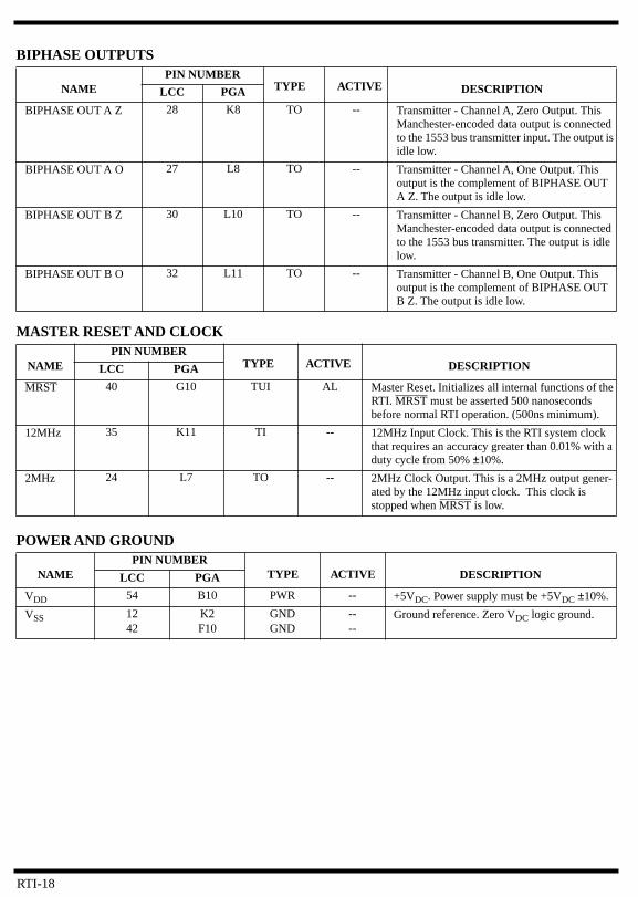
BIPHASE OUTPUTS
NAMEPIN NUMBER
DESCRIPTIONLCC PGA
BIPHASE OUT A Z 28 K8 TO -- Transmitter - Channel A, Zero Output. This Manchester-encoded data output is connected to the 1553 bus transmitter input. The output is idle low.
BIPHASE OUT A O 27 L8 TO -- Transmitter - Channel A, One Output. This output is the complement of BIPHASE OUT A Z. The output is idle low.
BIPHASE OUT B Z 30 L10 TO -- Transmitter - Channel B, Zero Output. This Manchester-encoded data output is connected to the 1553 bus transmitter. The output is idle low.
BIPHASE OUT B O 32 L11 TO -- Transmitter - Channel B, One Output. This output is the complement of BIPHASE OUT B Z. The output is idle low.
MASTER RESET AND CLOCK
NAMEPIN NUMBER
DESCRIPTIONLCC PGA
MRST 40 G10 TUI AL Master Reset. Initializes all internal functions of the RTI. MRST must be asserted 500 nanoseconds before normal RTI operation. (500ns minimum).
12MHz 35 K11 TI -- 12MHz Input Clock. This is the RTI system clock that requires an accuracy greater than 0.01% with a duty cycle from 50% ±10%.
2MHz 24 L7 TO -- 2MHz Clock Output. This is a 2MHz output gener-ated by the 12MHz input clock. This clock is stopped when MRST is low.
POWER AND GROUND
NAMEPIN NUMBER
DESCRIPTIONLCC PGA
VDD 54 B10 PWR -- +5VDC. Power supply must be +5VDC ±10%.
VSS 12 42
K2 F10
GNDGND
----
Ground reference. Zero VDC logic ground.
TYPE ACTIVE
TYPE ACTIVE
TYPE ACTIVE
RTI-18

CONTROL PINS
NAMEPIN NUMBER TYPE ACTIVE
DESCRIPTIONLCC PGA
CS 44 E9 TI AL Chip Select. Active low input for host access of transparent memory or the RTI internal registers. In the transparent memory configuration CS is propa-gated through the RTI to the RCS output.
CTRL 50 C11 TI AL Control. The host processor uses the active low CTRL input signal in conjunction with CS and RD/WR to access the RTI internal registers. CTRL is also used in the software assignment of the terminal address and programmed reset.
ADOEN 15 L3 TI AL Address Output Enable. When ADOEN is low the Address Out bus (ADDR OUT (15:0)) is active. If ADOEN = 1 the Address Out bus is high impedance.
RD/WR 46 E10 TI -- Read/Write. The host processor uses a high level on this input in conjunction with CS and CTRL to read the RTI internal registers. A low level on this input is used in conjunction with CS and CTRL to write to internal RTI registers. In the transparent memory configuration RD/WR is propagated through the RTI to the RRD/RWR output.
BCEN 25 K7 TUI AL Broadcast Enable. Active low input enables broad-cast commands.
ILL COMM 20 L5 TDI AH Illegal Command. The host processor uses the ILL COMM input to inform the RTI that the present command is illegal. ILL COMM is used in conjunc-tion with MCSA(4:0) and MC/SA to define system dependent illegal commands.
RTI-19

STATUS OUTPUTS
NAMEPIN NUMBER TYPE ACTIVE
DESCRIPTIONLCC PGA
RCS 43 F9 TO AL RAM Chip Select. Active low output used to enable memory for access.
RRD/RWR 45 E11 TO -- RAM Read/Write. High output enables memory read, low output enables memory write, used in conjunction with RCS). Normally high output.
COMSTR 22 J6 TO AL Command Strobe. COMSTR is an active low output of 500ns duration identifying receipt of a valid command.
TIMERON 41 G11 TO AL Fail-safe Timer. The TIMERON output pulses low for 730ms when the RTI begins transmit-ting (i.e., rising edge of STATUS) to provide a fail-safe timer meeting the requirements of MIL-STD-1553B. This pulse is reset when COMSTR goes low or during Master Reset. in the external self-test mode TIMERON does not recognize COMSTR and resets after 730ms.
MES ERR 49 D10 TO AH Message Error. The active high MES ERR out-put signals that the Message Error bit in the Sta-tus Register has been set due to receipt of an invalid command or an error during message sequence. MES ERR will reset to logic zero on receipt of next valid command.
CH A/B 26 L6 TO -- Channel A/B. Output identifying the channel on which the most recent valid command was received. Channel A = 1, Channel B = 0.
XMIT 38 H11 TO AL Transmit. Active low output identifies a transmit command message transfer by the RTI is in progress.
RCV 51 B11 TO AL Receive. Active low output identifies a receive command message transfer by the RTI is in progress.
BRDCST 36 J11 TO AL Broadcast. BRDCST is an active low output that identifies receipt of a valid broadcast com-mand.
STATUS 23 J7 TO AH Status. Active high output pulse indicating that the RTI is in the process of transmitting a status word.
RTI-20
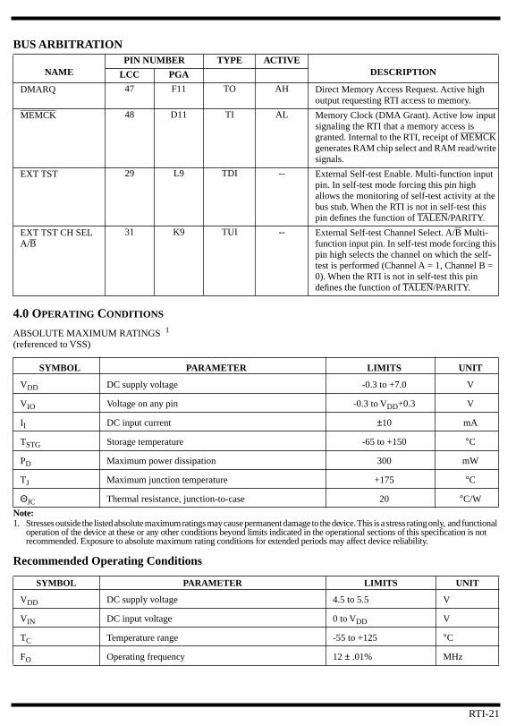
4.0 OPERATING CONDITIONS
ABSOLUTE MAXIMUM RATINGS 1 (referenced to VSS)
Recommended Operating Conditions
BUS ARBITRATION
NAMEPIN NUMBER TYPE ACTIVE
DESCRIPTIONLCC PGA
DMARQ 47 F11 TO AH Direct Memory Access Request. Active high output requesting RTI access to memory.
MEMCK 48 D11 TI AL Memory Clock (DMA Grant). Active low input signaling the RTI that a memory access is granted. Internal to the RTI, receipt of MEMCK generates RAM chip select and RAM read/write signals.
EXT TST 29 L9 TDI -- External Self-test Enable. Multi-function input pin. In self-test mode forcing this pin high allows the monitoring of self-test activity at the bus stub. When the RTI is not in self-test this pin defines the function of TALEN/PARITY.
EXT TST CH SEL A/B
31 K9 TUI -- External Self-test Channel Select. A/B Multi-function input pin. In self-test mode forcing this pin high selects the channel on which the self-test is performed (Channel A = 1, Channel B = 0). When the RTI is not in self-test this pin defines the function of TALEN/PARITY.
SYMBOL PARAMETER LIMITS UNIT
VDD DC supply voltage -0.3 to +7.0 V
VIO Voltage on any pin -0.3 to VDD+0.3 V
II DC input current ±10 mA
TSTG Storage temperature -65 to +150 °C
PD Maximum power dissipation 300 mW
TJ Maximum junction temperature +175 °C
ΘJC Thermal resistance, junction-to-case 20 °C/W
Note:1. Stresses outside the listed absolute maximum ratings may cause permanent damage to the device. This is a stress rating only, and functional
operation of the device at these or any other conditions beyond limits indicated in the operational sections of this specification is not recommended. Exposure to absolute maximum rating conditions for extended periods may affect device reliability.
SYMBOL PARAMETER LIMITS UNIT
VDD DC supply voltage 4.5 to 5.5 V
VIN DC input voltage 0 to VDD V
TC Temperature range -55 to +125 °C
FO Operating frequency 12 ± .01% MHz
RTI-21

5.0 DC ELECTRICAL CHARACTERISTICS (VDD = 5.0V ± 10%; -55°C < TC < +125°C)
SYMBOL PARAMETER CONDITION MINIMUM MAXIMUM UNIT
VIL Low-level input voltage 0.8 V
VIH High-level input voltage 2.0 V
IIN Input leakage current TTL inputs Inputs with pull-down resistorsInputs with pull-up resistors
VIN = VDD or VSS VIN = VDD VIN = VSS
-10110-2750
102750-110
µA µAµA
VOL Low-level output voltage IOL = 4mA 0.4 V
VOH High-level output voltage IOH = -400µA 2.4 V
IOZ Three-state output leakage current
VO = VDD or VSS -10 +10 µA
IOS Short-circuit output current 1, 2 VDD = 5.5V, VO = VDDVDD = 5.5V, VO = 0V -90
90 mAmA
CIN Input capacitance 3 ƒ = 1MHz @ 0V 10 pF
COUT Output capacitance 3 ƒ = 1MHz @ 0V 15 pF
CIO Bidirect I/O capacitance 3 ƒ = 1MHz @ 0V 25 pF
IDD Average operating current 1, 4 ƒ = 12MHz, CL = 50pF 50 mA
QIDD Quiescent current Note 5 1.5 mA
Notes: 1. Supplied as a design limit but not guaranteed or tested.2. Not more than one output may be shorted at a time for a maximum duration of one second. 3. Measured only for initial qualification, and after process or design changes that could affect input/output capacitance. 4. Includes current through input pull-ups. Instantaneous surge currents on the order of 1 ampere can occur during output switching.
Voltage supply should be adequately sized and decoupled to handle a large surge current. 5. All inputs with internal pull-ups or pull-downs should be left open circuit. All other inputs tied high or low.
SYNC
BIT TIMES
COMMAND WORD
5 5 5 1
DATA WORD 1
STATUS WORD
SYNC
SYNC
5
1
REMOTE TERMINAL ADDRESS
SUBADDRESS/MODE CODE
T/R DATA WORD COUNT/ MODE CODE
P
1 2 3 4 5 6 7 8 9 10 11 12 13 14 15 16 17 18 19 20
PDATA
1 1 1 1 1 1 1
Figure 8. MIL-STD-1553B Word Formats
16
REMOTE TERMINAL
ADDRESS
ME
SS
AG
E E
RR
OR
INS
TR
UM
EN
TAT
ION
SE
RV
ICE
RE
QU
ES
T
RESERVED
BR
OA
DC
AS
T C
OM
MA
ND
RE
CE
IVE
D
BU
SY
SU
BS
YS
TE
M F
LA
G
DY
NA
MIC
BU
S C
ON
TR
OL
AC
CE
PTA
NC
E
TE
RM
INA
L F
LA
G
PAR
ITY
1 1
RTI-22
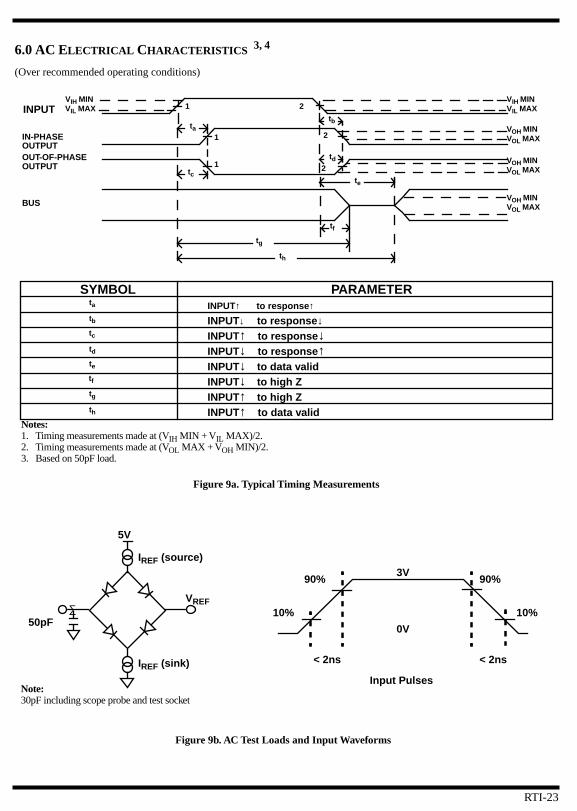
6.0 AC ELECTRICAL CHARACTERISTICS 3, 4
(Over recommended operating conditions)
to data valid to high Z
to response↑ to response↓ to response↓
INPUT↑INPUT↑INPUT↓INPUT↓INPUT↓INPUT↑INPUT↓
to high Z to data valid
INPUT↑ to response↑
PARAMETERSYMBOL
BUS
OUTPUTOUT-OF-PHASEOUTPUTIN-PHASE
INPUT
Notes:1. Timing measurements made at (VIH MIN + VIL MAX)/2.2. Timing measurements made at (VOL MAX + VOH MIN)/2.3. Based on 50pF load.
1 2
1 2
1 2
VIH MINVIL MAX
VIH MINVIL MAX
VOH MINVOL MAX
VOH MINVOL MAX
VOH MINVOL MAX
ta
tb
tc
td
te
tf
tg
th
tatb
tc
td
te
tf
tg
th
Figure 9a. Typical Timing Measurements
90%
Figure 9b. AC Test Loads and Input Waveforms
Note:30pF including scope probe and test socket
Input Pulses
10%10%
90%
< 2ns < 2ns
50pF
3V
0V
5V
∑
IREF (source)
VREF
IREF (sink)
RTI-23
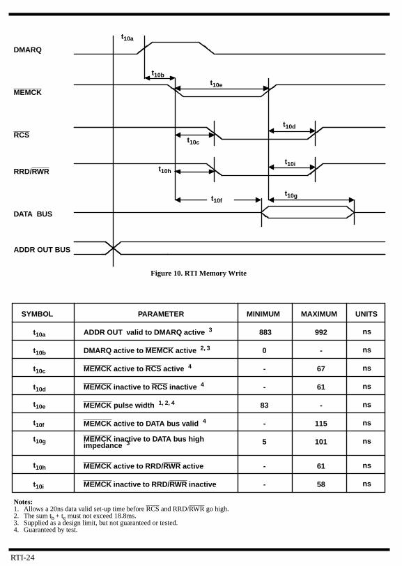
DMARQ
MEMCK
RCS
RRD/RWR
DATA BUS
ADDR OUT BUS
t10a
SYMBOL PARAMETER MINIMUM MAXIMUM UNITS
ADDR OUT valid to DMARQ active 3
DMARQ active to MEMCK active 2, 3
MEMCK active to RCS active 4
MEMCK inactive to RCS inactive 4
MEMCK active to RRD/RWR active
MEMCK inactive to RRD/RWR inactive
MEMCK pulse width 1, 2, 4
MEMCK active to DATA bus valid 4
MEMCK inactive to DATA bus high impedance 3
883 992
0 -
- 67
- 61
- 61
- 58
83 -
- 115
5 101
Notes:1. Allows a 20ns data valid set-up time before RCS and RRD/RWR go high.2. The sum tb + te must not exceed 18.8ms.3. Supplied as a design limit, but not guaranteed or tested.4. Guaranteed by test.
Figure 10. RTI Memory Write
ns
ns
ns
ns
ns
ns
ns
ns
ns
t10a
t10bt10e
t10c
t10h
t10f
t10d
t10i
t10g
t10b
t10c
t10d
t10e
t10f
t10g
t10h
t10i
RTI-24

DMARQ
MEMCK
RCS
DATA BUS
ADDR OUT BUS
SYMBOL PARAMETER MINIMUM MAXIMUM UNITS
ADDR OUT valid to DMARQ active 3
DMARQ active to MEMCK active 3
MEMCK active to RCS active 4
MEMCK inactive to RCS inactive 4
MEMCK pulse width 1, 2, 4
Input DATA valid to MEMCK inactive 4
Input DATA valid after RCS inactive 4
883 992
0
- 67
- 61
50 -
-45
5
Notes:1. Allows a 20ns data valid set-up time before RCS and RRD/RWR go high.2. The sum tb + te must not exceed 18.8ms.3. Supplied as a design limit, but not guaranteed or tested.4. Guaranteed by test.
Figure 11. RTI Memory Read
t11a
14.9
-
-
18.3
ns
ns
ns
ns
ns
ns
µs
µsDMARQ active to MEMCK inactive 4
t11h
t11bt11e
t11c
t11f
t11d
t11g
t11a
t11b
t11c
t11d
t11e
t11f
t11g
t11h
RTI-25

ADDR IN (0)
SYMBOL PARAMETER MINIMUM MAXIMUM UNITS
Input DATA valid before WRITE CONTROL inactive (set-up time) 3 20
Figure 12. Control Register Write Timing
ns
ns
ns
ns
DATA BUS
(CNTRL + CS + RD/WR)
t12c
25
20
20
-
-
-
-
WRITE CONTROL
Logical OR
Input DATA valid after WRITE CONTROL inactive (hold-time) 3
ADDR IN valid before WRITE CONTROL asserts 1, 3
ADDR IN valid after WRITE CONTROLnegates 2, 3
Notes:1. Set-up time required to prevent inadvertent software reset.2. Hold-time required to prevent inadvertent software reset.3. Guaranteed by test.
t12d
t12a t12b
t12a
t12b
t12c
t12d
RTI-26
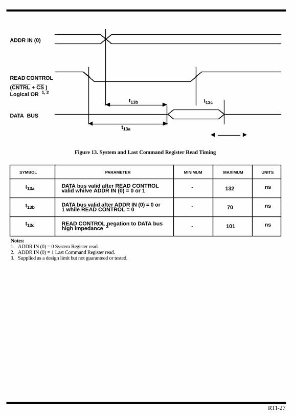
ADDR IN (0)
t13c
SYMBOL PARAMETER MINIMUM MAXIMUM UNITS
DATA bus valid after READ CONTROL valid whilve ADDR IN (0) = 0 or 1
Figure 13. System and Last Command Register Read Timing
ns
ns
ns
DATA BUS
(CNTRL + CS )
-
-
READ CONTROL
Logical OR 1, 2
DATA bus valid after ADDR IN (0) = 0 or 1 while READ CONTROL = 0
READ CONTROL negation to DATA bus high impedance 3
Notes:1. ADDR IN (0) = 0 System Register read.2. ADDR IN (0) = 1 Last Command Register read.3. Supplied as a design limit but not guaranteed or tested.
132
70
101-
t13b
t13a
t13a
t13b
t13c
RTI-27

TIMERON
SYMBOL PARAMETER MINIMUM MAXIMUM UNITS
STATUS active to TIMERON active 1
Figure 14. RT Fail-Safe Timer Signal Relationships
ns
ms
ms
BIPHASE OUT
-
-
STATUS
TIMERON active to first BIPHASE OUT transition 1
TIMERON low pulse width 1
Note:1. Supplied as a design limit, but not guaranteed or tested.
314
732
t14a
COMSTR
nsCOMSTR active to TIMERON reset 1 31
1.2
-
t14c
t14b
t14d
t14a
t14b
t14c
t14d
RTI-28
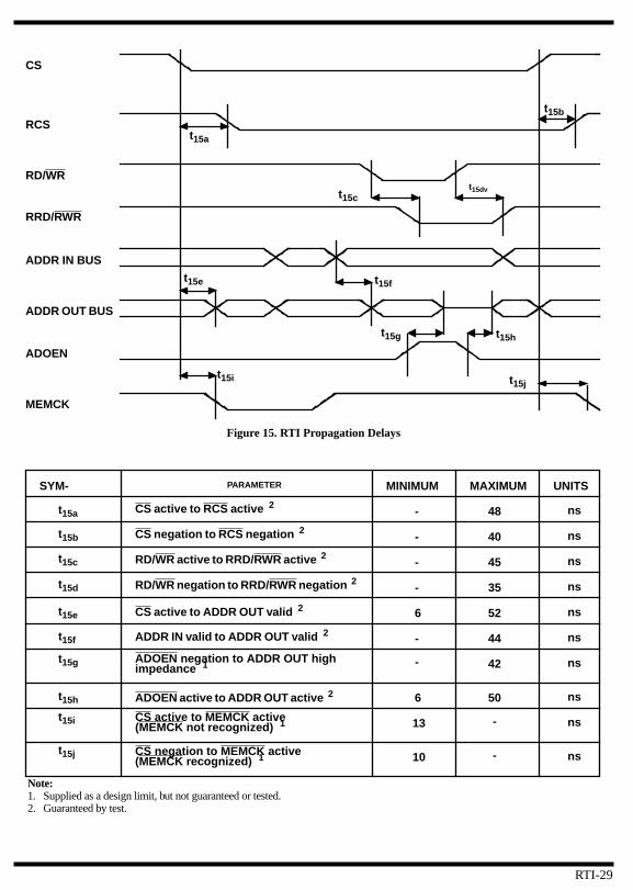
CS
RCS
ADOEN
ADDR IN BUS
Figure 15. RTI Propagation Delays
ADDR OUT BUS
MEMCK
SYM- PARAMETER MINIMUM MAXIMUM UNITS
CS active to RCS active 2
CS negation to RCS negation 2
RD/WR active to RRD/RWR active 2
RD/WR negation to RRD/RWR negation 2
ADOEN active to ADDR OUT active 2
CS active to ADDR OUT valid 2
ADDR IN valid to ADDR OUT valid 2
ADOEN negation to ADDR OUT highimpedance 1
48
- 45
- 35
6
6
- 44
42
50
Note:1. Supplied as a design limit, but not guaranteed or tested.2. Guaranteed by test.
ns
ns
ns
ns
ns
ns
ns
ns
t15a
RD/WR
RRD/RWR
-
CS active to MEMCK active(MEMCK not recognized) 1 13 ns-
CS negation to MEMCK active(MEMCK recognized) 1 10 ns-
-
- 40
52
t15a
t15e
t15i
t15c
t15f
t15g t15h
t15j
t15dv
t15b
t15b
t15c
t15d
t15e
t15f
t15g
t15h
t15i
t15j
RTI-29

COMSTR
Figure 16. Command Word Validation
t16aBIPHASE IN
RCV
XMIT
CH A/B
PCOMMAND
BRDCST
MC/SA
MCSA(4:0)
ADDR OUT 1
MESS ERR
SYMBOL PARAMETER MINIMUM MAXIMUM UNITS
Command word parity to COMSTR and RCV or XMIT active 4
COMSTR pulse width 4
Command word parity to CH A/B valid 4
Status output signals valid to COMSTRactive 2, 4
MES ERR reset after COMSTR active 4
3.67
-430
745
µs
µs
ns
ns
3.58
2.58 2.66
750
Notes:1. ADOEN is asserted (i.e., logic low).2. Status signals include BRDCST, MC/SA, MCSA(4:0), and ADDR OUT.3. Measured from mid-bit parity crossing.4. Supplied as a design limit, but not guaranteed or tested.
3
499 502 ns
t16b
t16c
t16d t16e
t16a
t16b
t16c
t16d
t16e
RTI-30
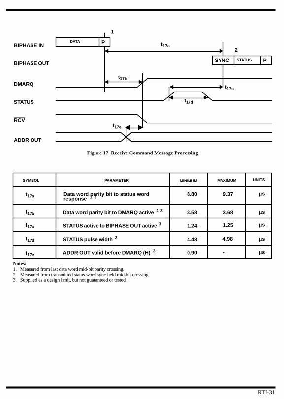
Figure 17. Receive Command Message Processing
BIPHASE IN
DMARQ
STATUS
PDATA
SYMBOL PARAMETER MINIMUM MAXIMUM UNITS
Data word parity bit to status word response 1, 3
Data word parity bit to DMARQ active 2, 3
STATUS active to BIPHASE OUT active 3
STATUS pulse width 3
9.37
4.984.48
µs
µs
µs
8.80
3.58 3.68
Notes:1. Measured from last data word mid-bit parity crossing.2. Measured from transmitted status word sync field mid-bit crossing.3. Supplied as a design limit, but not guaranteed or tested.
1
BIPHASE OUTPSTATUS
2
SYNC
t17a
RCV
1.24 1.25 µs
ADDR OUT
ADDR OUT valid before DMARQ (H) 3 -0.90 µs
t17b
t17c
t17d
t17e
t17a
t17b
t17c
t17d
t17e
RTI-31

Figure 18. Transmitted Data Timing
DMARQ
SYM- PARAMETER MINIMUM MAXIMUM UNITS
DMARQ active to sync field of transmitted data word
DMARQ active to DMARQ active
XMIT negation after last DMARQ active
17.18 µs
µs
17.15
- 19.2
Note:* Supplied as a design limit but not guaranteed or tested.
BIPHASE
460 500 µs
t18a
t18c
t18b
* t18a
* t18b
* t18c
20 200 0
XMIT
RTI-32
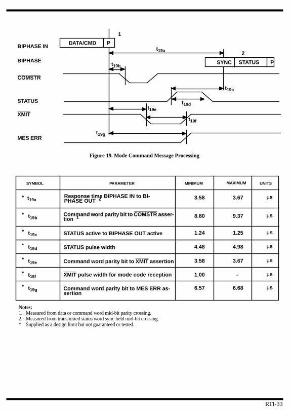
Figure 19. Mode Command Message Processing
BIPHASE INDATA/CMD
SYMBOL PARAMETER MINIMUM MAXIMUM UNITS
Response time BIPHASE IN to BI-PHASE OUT 2
Command word parity bit to COMSTR asser-tion 1
3.67 µs
µs
3.58
8.80 9.37
Notes:1. Measured from data or command word mid-bit parity crossing.2. Measured from transmitted status word sync field mid-bit crossing.* Supplied as a design limit but not guaranteed or tested.
1
BIPHASE
t19a
MES ERR
*
*
t19g
t19a
t19b
PSTATUSSYNC
2
t19c
t19b
t19e
t19f
t19d
STATUS active to BIPHASE OUT active µs1.24 1.25* t19c
STATUS pulse width µs4.48 4.98* t19d
Command word parity bit to XMIT assertion µs3.58 3.67* t19e
XMIT pulse width for mode code reception µs1.00 -* t19f
Command word parity bit to MES ERR as-sertion
µs6.57 6.68* t19g
COMSTR
STATUS
XMIT
P
RTI-33

Figure 20. Message Error
BIPHASE IN PDATA
SYMBOL PARAMETER MINIMUM MAXIMUM UNITS
Data word parity bit to MES ERR assertion 1
Command word parity bit to MES ERR assertion RT to RT transfer 2
23.63 µs
µs
23.50
55.4 55.5
Notes:1. Measured from last data word mid-bit parity crossing.2. No response from transmitter.* Supplied as a design limit but not guaranteed or tested.
1
MES ERR
t20a
BIPHASE IN PRCV CMD
1
PXMIT CMD
MES ERR
*
*
t20b
t20a
t20b
RTI-34

UT1553BRTI
HOST SUBSYSTEM
ADDR IN (10:0)
DATA(15:0)
CONTROL
UT63M1251553 TRANSCEIVER
1553 BUS A
1553 BUS B
Figure 21. RTI General System Diagram (Idle low interface)
Figure 22. RTI Transceiver Interface Diagram
BIPHASECHANNEL A
BIPHASECHANNEL B
RTI
IN OIN Z
OUT OOUT Z
TIMERON
UTMC63M125
CHANNEL A
CHANNEL B
TXIN-
TXINHB
RXOUTRXOUT
TXINTXIN
RXOUTRXOUT
TXINTXIN
IN OIN Z
OUT OOUT Z
CH A/BLOGIC
RTI-35
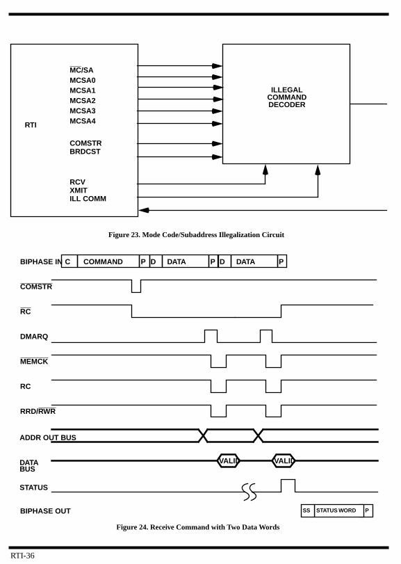
ILLEGALCOMMANDDECODER
RTI
Figure 23. Mode Code/Subaddress Illegalization Circuit
MC/SAMCSA0MCSA1MCSA2MCSA3MCSA4
COMSTRBRDCST
RCVXMITILL COMM
PCOMMAND C
PSTATUS WORDSS
BIPHASE IN
BIPHASE OUT
RC
COMSTR
DMARQ
MEMCK
RC
RRD/RWR
ADDR OUT BUS
DATA BUS
STATUS
VALID VALID
Figure 24. Receive Command with Two Data Words
D DATA P D DATA P
RTI-36
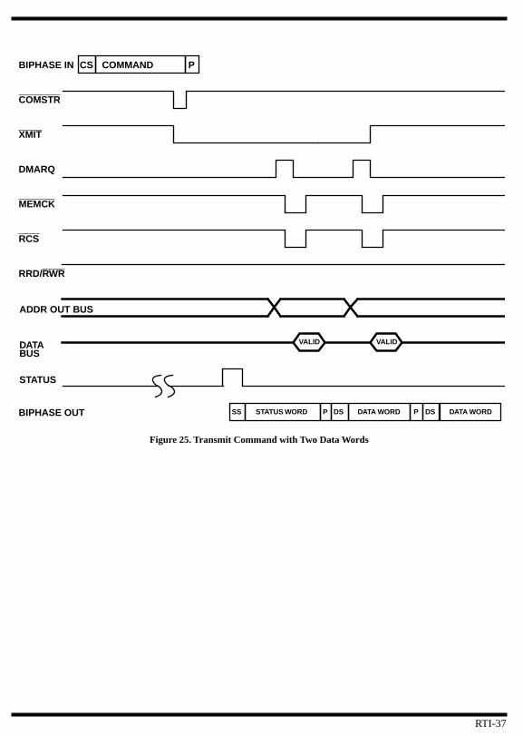
PCOMMAND CS
DS DATA WORD PPSTATUS WORDSS DS DATA WORD
BIPHASE IN
BIPHASE OUT
XMIT
COMSTR
DMARQ
MEMCK
RCS
RRD/RWR
ADDR OUT BUS
DATA BUS
STATUS
VALID VALID
Figure 25. Transmit Command with Two Data Words
RTI-37
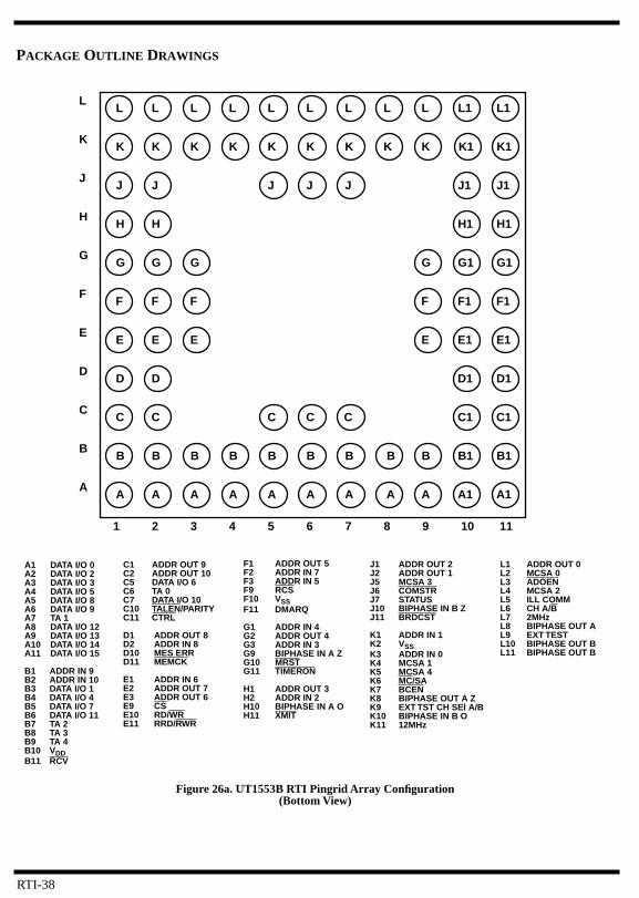
PACKAGE OUTLINE DRAWINGS
LL
K
H
G
F
E
D
C
B
A
1 2 3 4 5 6 7 8 9 10 11
Figure 26a. UT1553B RTI Pingrid Array Configuration (Bottom View)
L L L L L L L L L1 L1
K K K K K K K K K K1 K1
JJ J J1 J1
H H H1 H1
G G G1 G1
F F F1 F1
E E E1 E1
D D D1 D1
C C C1 C1
B B B B B B B B B B1 B1
A A A A A A A A A A1 A1
C C C
J J J
G
F
E
G
F
E
F1 ADDR OUT 5 F2 ADDR IN 7F3 ADDR IN 5F9 RCSF10 VSSF11 DMARQ
G1 ADDR IN 4G2 ADDR OUT 4G3 ADDR IN 3G9 BIPHASE IN A ZG10 MRSTG11 TIMERON
H1 ADDR OUT 3H2 ADDR IN 2H10 BIPHASE IN A OH11 XMIT
C1 ADDR OUT 9C2 ADDR OUT 10C5 DATA I/O 6C6 TA 0C7 DATA I/O 10C10 TALEN/PARITYC11 CTRL
D1 ADDR OUT 8D2 ADDR IN 8D10 MES ERRD11 MEMCK
E1 ADDR IN 6E2 ADDR OUT 7E3 ADDR OUT 6E9 CSE10 RD/WRE11 RRD/RWR
A1 DATA I/O 0A2 DATA I/O 2A3 DATA I/O 3A4 DATA I/O 5A5 DATA I/O 8A6 DATA I/O 9A7 TA 1A8 DATA I/O 12A9 DATA I/O 13A10 DATA I/O 14A11 DATA I/O 15
B1 ADDR IN 9B2 ADDR IN 10B3 DATA I/O 1B4 DATA I/O 4B5 DATA I/O 7B6 DATA I/O 11B7 TA 2B8 TA 3B9 TA 4B10 VDDB11 RCV
J1 ADDR OUT 2J2 ADDR OUT 1J5 MCSA 3J6 COMSTRJ7 STATUSJ10 BIPHASE IN B ZJ11 BRDCST
K1 ADDR IN 1K2 VSSK3 ADDR IN 0K4 MCSA 1K5 MCSA 4K6 MC/SAK7 BCENK8 BIPHASE OUT A ZK9 EXT TST CH SEl A/BK10 BIPHASE IN B OK11 12MHz
L1 ADDR OUT 0L2 MCSA 0L3 ADOENL4 MCSA 2L5 ILL COMML6 CH A/BL7 2MHzL8 BIPHASE OUT A L9 EXT TESTL10 BIPHASE OUT B L11 BIPHASE OUT B
RTI-38
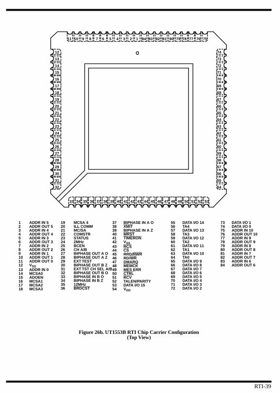
1 ADDR IN 52 ADDR OUT 53 ADDR IN 44 ADDR OUT 45 ADDR IN 36 ADDR OUT 37 ADDR IN 28 ADDR OUT 29 ADDR IN 110 ADDR OUT 111 ADDR OUT 012 VSS13 ADDR IN 014 MCSA015 ADOEN16 MCSA117 MCSA218 MCSA3
73 DATA I/O 174 DATA I/O 075 ADDR IN 1076 ADDR OUT 1077 ADDR IN 978 ADDR OUT 979 ADDR IN 880 ADDR OUT 881 ADDR IN 782 ADDR OUT 783 ADDR IN 684 ADDR OUT 6
19 MCSA 420 ILL COMM21 MC/SA22 COMSTR23 STATUS24 2MHz25 BCEN26 CH A/B27 BIPHASE OUT A O28 BIPHASE OUT A Z29 EXT TEST30 BIPHASE OUT B Z31 EXT TST CH SEL A/B32 BIPHASE OUT B O33 BIPHASE IN B O34 BIPHASE IN B Z35 12MHz36 BRDCST
37 BIPHASE IN A O38 XMIT39 BIPHASE IN A Z40 MRST41 TIMERON42 VSS43 RCS44 CS45 RRD/RWR46 RD/WR47 DMARQ48 MEMCK49 MES ERR50 CTRL51 RCV52 TALEN/PARITY53 DATA I/O 1554 VDD
55 DATA I/O 1456 TA457 DATA I/O 1358 TA359 DATA I/O 1260 TA261 DATA I/O 1162 TA163 DATA I/O 1064 TA065 DATA I/O 966 DATA I/O 867 DATA I/O 768 DATA I/O 669 DATA I/O 570 DATA I/O 471 DATA I/O 372 DATA I/O 2
73
72
71
70
69
68
67
66
65
64
63
62
61
60
59
58
57
56
55
54
535251504948474645444342414039383736353433
16
19
32
31
30
29
28
27
26
25
24
23
22
21
20
18
17
15
14
13
12 74
11 10 9 8 7 6 5 4 3 2 1 84 83 82 81 80 79 78 77 76 75
Figure 26b. UT1553B RTI Chip Carrier Configuration(Top View)
RTI-39
Packaging-1
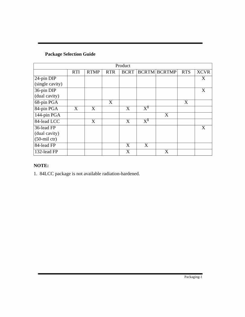
Package Selection Guide
NOTE:
1. 84LCC package is not available radiation-hardened.
ProductRTI RTMP RTR BCRT BCRTM BCRTMP RTS XCVR
24-pin DIP(single cavity)
X
36-pin DIP(dual cavity)
X
68-pin PGA X X84-pin PGA X X X X1
144-pin PGA X84-lead LCC X X X1
36-lead FP(dual cavity)(50-mil ctr)
X
84-lead FP X X132-lead FP X X

Packaging-2
1
144-Pin Pingrid Array
E1.565 ± 0.025
-B-
D1.565 ± 0.025 -A-
0.080 REF.(2 Places)
0.040 REF.
0.100 REF.(4 Places)
A0.130 MAX.
Q0.050 ± 0.010 A
A
L0.130 ±0.010
PIN 1 I.D.(Geometry Optional)
-C-(Base Plane)
b0.018 ± 0.002
0.0300.010
C A BC
SIDE VIEW
TOP VIEW
0.003 MIN. TYP.
D1/E11.400
0.100TYP.
e
PIN 1 I.D.(Geometry Optional)
2R
P
N
M
L
K
J
H
G
F
E
D
1 2 3 4 5 6 7 8 9 10 11 12 13 14 15
Notes:1. True position applies to pins at base plane (datum C).2. True position applies at pin tips.3. All package finishes are per MIL-M-38510.4. Letter designations are for cross-reference to MIL-M-38510.
BOTTOM VIEW

Packaging-3
132-Lead Flatpack (25-MIL Lead Spacing)
SIDE VIEW
TOP VIEW
BOTTOM VIEW A-A
DETAIL A
0.018 MAX. REF.0.014 MAX. REF.(At Braze Pads)
L0.250MIN.REF.
LEAD KOVAR
SEE DETAIL AA
A
C0.005 + 0.002
- 0.001
A0.1100.006D1/E1
0.950 ± 0.015 SQ.
D/E1.525 ± 0.015 SQ.
PIN 1 I.D.(GeometryOptional)
e0.025
Notes:1. All package finishes are per MIL-M-38510.2. Letter designations are for cross-reference to MIL-M-38510.
S1
0.005 MIN. TYP.

Packaging-4
84-LCC
SIDE VIEWTOP VIEW
BOTTOM VIEW A-A
Notes:1. All package finishes are per MIL-M-38510.2. Letter designations are for cross-reference to MIL-M-38510.
L/L10.050 ± 0.005 TYP.
B10.025 ± 0.003
e0.050
e10.015 MIN.
PIN 1 I.D.(Geometry Optional)
J0.020 X 455 REF.
h0.040 x 45_REF. (3 Places)
D/E1.150 ± 0.015 SQ.
A0.115 MAX.
A10.080 ± 0.008 A
APIN 1 I.D.
(Geometry Optional)

Packaging-5
84-Lead Flatpack (50-MIL Lead Spacing)
SIDE VIEW
TOP VIEW
BOTTOM VIEW A-A
D/E1.810 ± 0.015 SQ.
Notes:1. All package finishes are per MIL-M-38510.2. Letter designations are for cross-reference to MIL-M-38510.
DETAIL A
D1/E11.150 ± 0.012 SQ.
A0.1100.060
A
A
C0.007 ± 0.001
LEAD KOVAR
SEE DETAIL A
PIN 1 I.D.(GeometryOptional)
b0.016 ± 0.002
L0.260MIN.REF.
S10.005 MIN. TYP.
0.050e
0.014 MAX. REF.
(At Braze Pads)
0.018 MAX. REF.
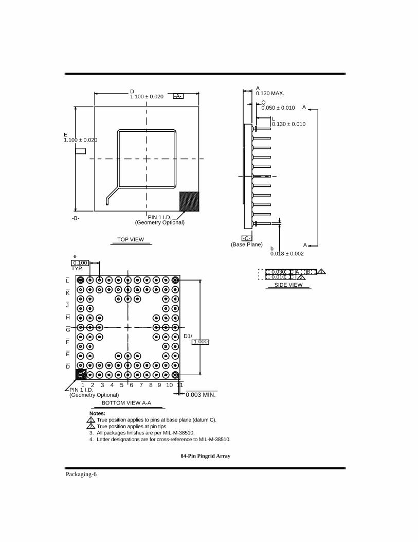
Packaging-6
84-Pin Pingrid Array
SIDE VIEW
TOP VIEW
BOTTOM VIEW A-A
D1.100 ± 0.020
E1.100 ± 0.020
-B-
-A-
A0.130 MAX.
Q0.050 ± 0.010
L0.130 ± 0.010
A
A
-C-(Base Plane)
b0.018 ± 0.002
PIN 1 I.D.(Geometry Optional)
1.000D1/
e0.100
TYP.
0.003 MIN.
L
K
J
H
G
F
E
D
1 2 3 4 5 6 7 8 9 10 11
Notes:1. True position applies to pins at base plane (datum C).2. True position applies at pin tips.3. All packages finishes are per MIL-M-38510.4. Letter designations are for cross-reference to MIL-M-38510.
PIN 1 I.D.(Geometry Optional)
10.0300.010
C A BC 2

Packaging-7
SIDE VIEW
TOP
BOTTOM VIEW A-A
D1.100 ± 0.020
PIN 1 I.D.(Geometry Optional)
LKJHGFEDCBA
1 2 3 4 5 6 7 8 9 10 11
Notes:1 True position applies to pins at base plane (datum C).2 True position applies at pin tips.3. All packages finishes are per MIL-M-38510.4. Letter designations are for cross-reference to MIL-M-38510.
PIN 1 I.D.(Geometry Optional)
D1/E11.00
0.003 MIN. TYP.
e0.100TYP.
A0.130 MAX.
Q0.050 ± 0.010
L0.130 ± 0.010
A
A
-A-
-B-
E1.100 ± 0.020
-C-(Base Plane)
68-Pin Pingrid Array
0.0300.010 C
A B 12
C∅∅
b
0.010 ± 0.002

Packaging-8
D1.800 ± 0.025
36-Lead Flatpack, Dual Cavity (100-MIL Lead Spacing)
TOP VIEW
END VIEW
E0.750 ± 0.015
Notes:1 All package finishes are per MIL-M-38510.2. It is recommended that package ceramic be mounted to
a heat removal rail located on the printed circuit board. A thermally conductive material such as MERECO XLN-589 or equivalent should be used.
3. Letter designations are for cross-reference to MIL-M-38510.
PIN 1 I.D.(Geometry Optional)
L0.490MIN.
b0.015 ± 0.002
e0.10
c0.008 + 0.002
- 0.001
Q0.080 ± 0.010(At Ceramic Body)
A0.130 MAX.

Packaging-9
36-Lead Flatpack, Dual Cavity (50-MIL Lead Spacing)
TOP
E0.700 + 0.015
Notes:1. All package finishes are per MIL-M-38510.2. It is recommended that package ceramic be mounted to
a heat removal rail located on the printed circuit board.A thermally conductive material such as MERECO XLN-589 or equivalent should be used.
3. Letter designations are for cross-reference to MIL-M-38510.
c0.007
+ 0.002 - 0.001
Q0.070 + 0.010(At Ceramic Body)
A0.100 MAX.
END
D1.000 ± 0.025
b0.016 + 0.002
e0.050
PIN 1 I.D(Geometry Optional)
L0.330MIN.
Packaging-10
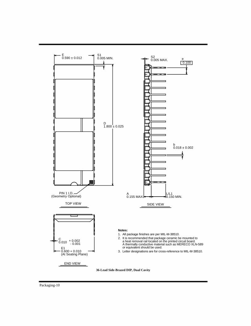
36-Lead Side-Brazed DIP, Dual Cavity
TOP VIEW
END VIEW
E0.590 ± 0.012
Notes:1. All package finishes are per MIL-M-38510.2. It is recommended that package ceramic be mounted to
a heat removal rail located on the printed circuit board.A thermally conductive material such as MERECO XLN-589 or equivalent should be used.
3. Letter designations are for cross-reference to MIL-M-38510.
PIN 1 I.D.(Geometry Optional)
SIDE VIEW
S10.005 MIN.
D1.800 ± 0.025
S20.005 MAX. e
0.100
A0.155 MAX.
L/L10.150 MIN.
C0.010 + 0.002
- 0.001E10.600 + 0.010(At Seating Plane)
b0.018 ± 0.002

Packaging-11
E0.590 ± 0.015
S10.005 MIN. S2
0.005 MAX.
TOP VIEW
PIN 1 I.D.(Geometry Optional)
D1.200 ± 0.025
SIDE VIEW
A0.140 MAX.
L/L10.150 MIN.
0.100e
Notes:1. All package finishes are per MIL-M-38510.2. It is recommended that package ceramic be mounted to
a heat removal rail located on the printed circuit board.A thermally conductive material such as MERECO XLN-589 or equivalent should be used.
3. Letter designations are for cross-reference to MIL-M-38510.
END VIEW
C0.010
+ 0.002 - 0.001
E10.600 + 0.010(At Seating Plane)
b0.018 ± 0.002
24-Lead Side-Brazed DIP, Single Cavity

ORDERING INFORMATION
UT1553B RTI Remote Terminal Interface:
Lead Finish:(A) = Solder (C) = Gold(X) = Optional
Case Outline:(Z) = 84 pin PGA
Class Designator:(B) = Jan Class Q
Device Type01 = 10% to 35% Clock Duty Cycle
Drawing Number: JM38510/555
Total Dose:(-) = None Federal Stock Class Designator: No options
5962 * * * * * *
Notes:1. Lead finish (A, C, or X) must be specified.2. If an "X" is specified when ordering, part marking will match the lead finish and will be either "A" (solder) or "C" (gold).

UT1553B RTI Remote Terminal Interface
Lead Finish:(A) = Solder (C) = Gold(X) = Optional
Screening:(C) = Military Temperature(P) = Prototype
Package Type:(G) = 84 pin PGA
Modifier:RTI = 10% to 35% Clock Duty Cycle
UTMC Core Part Number
UT1553B - * * * *
Notes:1. Lead finish (A, C, or X) must be specified. 2. If an "X" is specified when ordering, part marking will match the lead finish and will be either "A" (solder) or "C" (gold).3. Mil Temp range flow per UTMC’s manufacturing flows document. Devices are tested at -55°C, room temperature, and 125°C.4. Prototpe flow per UTMC’s document manufacturing flows and are tested at 25°C only. Lead finish is GOLD only.5. Prototypes and reduced high-reliability devices are only available with 40% to 60% clock duty cycle.

![Response to Intervention (RtI) Handbook and RtI Resources · 2016-12-09 · OASD RtI Handbook [2] Response to Intervention (RtI) Overview Core Principles of RtI RtI is grounded in](https://img.pdfslide.us/doc/110x75/5f04175d7e708231d40c46b9/response-to-intervention-rti-handbook-and-rti-resources-2016-12-09-oasd-rti.jpg)