Embed Size (px)
Citation preview
Using the UCD3138PFCEVM-026
User's Guide
Literature Number: SLUU885B
March 2012–Revised July 2012
www.ti.com
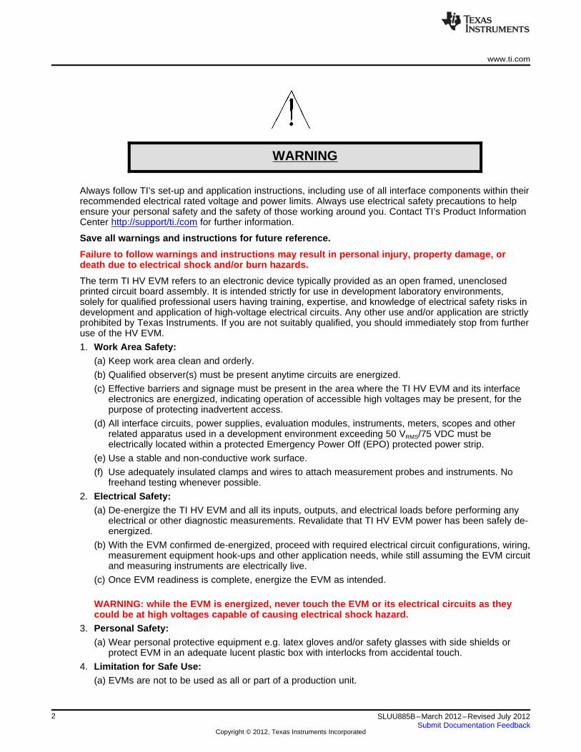
WARNING
Always follow TI’s set-up and application instructions, including use of all interface components within theirrecommended electrical rated voltage and power limits. Always use electrical safety precautions to helpensure your personal safety and the safety of those working around you. Contact TI’s Product InformationCenter http://support/ti./com for further information.
Save all warnings and instructions for future reference.
Failure to follow warnings and instructions may result in personal injury, property damage, ordeath due to electrical shock and/or burn hazards.
The term TI HV EVM refers to an electronic device typically provided as an open framed, unenclosedprinted circuit board assembly. It is intended strictly for use in development laboratory environments,solely for qualified professional users having training, expertise, and knowledge of electrical safety risks indevelopment and application of high-voltage electrical circuits. Any other use and/or application are strictlyprohibited by Texas Instruments. If you are not suitably qualified, you should immediately stop from furtheruse of the HV EVM.
1. Work Area Safety:(a) Keep work area clean and orderly.
(b) Qualified observer(s) must be present anytime circuits are energized.
(c) Effective barriers and signage must be present in the area where the TI HV EVM and its interfaceelectronics are energized, indicating operation of accessible high voltages may be present, for thepurpose of protecting inadvertent access.
(d) All interface circuits, power supplies, evaluation modules, instruments, meters, scopes and otherrelated apparatus used in a development environment exceeding 50 VRMS/75 VDC must beelectrically located within a protected Emergency Power Off (EPO) protected power strip.
(e) Use a stable and non-conductive work surface.
(f) Use adequately insulated clamps and wires to attach measurement probes and instruments. Nofreehand testing whenever possible.
2. Electrical Safety:(a) De-energize the TI HV EVM and all its inputs, outputs, and electrical loads before performing any
electrical or other diagnostic measurements. Revalidate that TI HV EVM power has been safely de-energized.
(b) With the EVM confirmed de-energized, proceed with required electrical circuit configurations, wiring,measurement equipment hook-ups and other application needs, while still assuming the EVM circuitand measuring instruments are electrically live.
(c) Once EVM readiness is complete, energize the EVM as intended.
WARNING: while the EVM is energized, never touch the EVM or its electrical circuits as theycould be at high voltages capable of causing electrical shock hazard.
3. Personal Safety:(a) Wear personal protective equipment e.g. latex gloves and/or safety glasses with side shields or
protect EVM in an adequate lucent plastic box with interlocks from accidental touch.
4. Limitation for Safe Use:(a) EVMs are not to be used as all or part of a production unit.
2 SLUU885B–March 2012–Revised July 2012Submit Documentation Feedback
Copyright © 2012, Texas Instruments Incorporated
User's GuideSLUU885B–March 2012–Revised July 2012
Digitally Controlled Single-Phase PFC Pre-Regulator
1 Introduction
This EVM is to help evaluate the UCD3138 64-pin digital control device in off-line power converterapplication and then to aid its design. The EVM is a standalone Power Factor Correction (PFC) pre-regulator of single-phase AC input. The EVM UCD3138PFCEVM-026 is used together with its controlcard, UCD3138CC64EVM-030, also an EVM on which is placed UCD3138RGC.
The EVM of UCD3138PFCEVM-026 together with UCD3138CC64EVM-030 can be used as they aredelivered without additional work, from either hardware or firmware, to evaluate PFC. TheUCD3138PFCEVM-026 together with the UCD3138CC64EVM-030 can also be re-tuned on its designparameters through the operation of GUI, called Texas Instruments Fusion Digital Power Designer, or re-loaded up with custom firmware with user’s definition and development.
The EVM system is in topology of single-phase boost converter at its delivery on both hardware andfirmware, but can be re-configured into two other PFC topologies: dual-phase interleaved, and bridgeless,then corresponding operation can be made by reloading with that associated firmware. All necessity ofhardware and firmware for the two additional topologies are already developed and delivered with theshipment. Please contact Texas Instruments to obtain the instructions how to make re-configuration.
In the package delivered, three EVMs are included UCD3138PFCEVM-026, UCD3138CC64EVM-030, andUSB-TO-GPIO. In the same package, also included is a hard copy of Evaluation Module Electrical SafetyGuideline.
This user’s guide provides basic evaluation instruction from a viewpoint of system operation in standalonePFC in its boost configuration.
3SLUU885B–March 2012–Revised July 2012 Digitally Controlled Single-Phase PFC Pre-RegulatorSubmit Documentation Feedback
Copyright © 2012, Texas Instruments Incorporated

Description www.ti.com
2 Description
UCD3138PFCEVM-026 together with UCD3138CC64EVM-030 is an EVM of PFC pre-regulator with digitalcontrol using UCD3138 device in boost converter topology and in the application of single-phase AC input.UCD3138 device is located on the board of UCD3138CC64EVM-030. UCD3138CC64EVM-030 is adaughter card and serves all PFC required control functions with preloaded single-phase boost PFCfirmware. UCD3138PFCEVM-026 accepts universal AC line input from 90 VAC to 264 VAC, and outputsnominal 390 VDC with full load output power 360 W, or full output current 0.92 A.
2.1 Typical Applications• Single-Phase Universal AC Line Power Factor Correction Pre-Regulator
• Servers
• Telecommunication Systems
2.2 Features• Digitally Controlled PFC Pre-Regulator
• Universal AC Line Input from 90 VAC to 264 VAC with AC Line Frequency 47 Hz to 63 Hz
• Regulated Output 390 VDC with Output from No-Load to Full-Load
• Full-Load Power 360 W, or full-Load Current 0.92 A
• High Power Factor Close to 0.999 and Low THD Below 5% in Most Operation Conditions
• High Efficiency
• Protection:
– Over Voltage
– Over Current
– Brownout
– Power-On Inrush Current
• Test Points to Facilitate Device and Topology Evaluation
• Re-Configurable to Dual-Phase Interleaved PFC or Bridgeless PFC (please contact TI for detail)
4 Digitally Controlled Single-Phase PFC Pre-Regulator SLUU885B–March 2012–Revised July 2012Submit Documentation Feedback
Copyright © 2012, Texas Instruments Incorporated
www.ti.com Electrical Performance Specifications
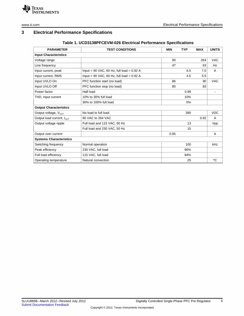
3 Electrical Performance Specifications
Table 1. UCD3138PFCEVM-026 Electrical Performance Specifications
PARAMETER TEST CONDITIONS MIN TYP MAX UNITS
Input Characteristics
Voltage range 90 264 VAC
Line frequency 47 63 Hz
Input current, peak Input = 90 VAC, 60 Hz, full load = 0.92 A 6.5 7.0 A
Input current, RMS Input = 90 VAC, 60 Hz, full load = 0.92 A 4.5 5.5
Input UVLO On PFC function start (no load) 86 90 VAC
Input UVLO Off PFC function stop (no load) 80 83
Power factor Half load 0.99 -
THD, input current 10% to 30% full load 10%
30% to 100% full load 5%
Output Characteristics
Output voltage, VOUT No load to full load 390 VDC
Output load current, IOUT 90 VAC to 264 VAC 0.92 A
Output voltage ripple Full load and 115 VAC, 60 Hz 13 Vpp
Full load and 230 VAC, 50 Hz 15
Output over current 0.95 A
Systems Characteristics
Switching frequency Normal operation 100 kHz
Peak efficiency 230 VAC, full load 96%
Full load efficiency 115 VAC, full load 94%
Operating temperature Natural convection 25 ºC
5SLUU885B–March 2012–Revised July 2012 Digitally Controlled Single-Phase PFC Pre-RegulatorSubmit Documentation Feedback
Copyright © 2012, Texas Instruments Incorporated
DP
WM
_3
B
FA
ULT
_0
SC
I_T
X1
PW
M-1
SC
I_R
X0
GN
D_
Ext
FA
ULT
_1
SY
NC
SC
I_R
X1
PW
M-0
SC
I_T
X0
3.3
V
Ext S
upply
AD
_0
1
AD
_0
2
AD
_0
5
AD
_0
7
AD
_0
8
EA
DC
_P
2
EA
DC
_P
1
Wh
en
U11
no
t in
sta
lled
, co
nn
ect
J1
4-1
an
d -
3 t
o e
xte
rna
l so
urc
e t
o g
et
+1
2V
_E
XT
Vin
= 9
0 to 2
64 V
ac (
47 to 6
3H
z)
Copper
fill
for
heat-
sin
k
AD
_0
0
AD
_0
3
AD
_0
4
AD
_0
6
EA
DC
_P
0
Isola
ted G
ND
OP
TO
Isola
ted S
ection
Isola
ted G
ND
R3
1 a
nd
R1
06
are
pre
loa
d r
esis
tors
If n
ee
de
d,
co
nn
ect
J1
5-1
an
d -
2 t
o u
se
U11
to
bia
s s
eco
nd
ary
sid
e
Exte
rnal sync s
ignal
Bridgele
ss P
FC
with C
T_1 a
nd C
T_2 a
nd Inte
rleaved P
FC
with IS
EN
SE
_S
HU
NT.
Part
s n
ot used
AD
_1
3
3 1
4 2
12
12
1
111
1
11
1
1
AG
ND
DG
ND
1
AC
_Lin
e
AC
_N
eutr
al
if u
se
VA
UX
_P
bu
t n
ot
use
VA
UX
_S
Se
co
nd
ary
sid
eIs
ola
tio
n lin
e
Fuse:T
7A
/250V
AC
(J3-1
3)
(J3-2
5)
(J3-2
6)
(J4-1
8)
(J4-2
0)
(J3-1
1)
(J3-8
)
Secondary
sid
e
Secondary
sid
e
1
TP
8
TP
9
TP
12
TP
13
TP
10
1 2
J7
R31
1.5
k
C5
4.7
nF
R19
4.7
k
+C
1
10uF
TP
11
C3
47nF
D18
C37
0.4
7uF
D21
TP
4
R14
3.8
3k
R13
200k
R27
200k
D20
C20
1nF
R16
3.8
3k
R29
200k
R15
200k TP
3
1
234
5
K1
R68
C25
R24
R78
1.1
k
TP
2
TP
1
1 2 3
J10
F2
R20
4.7
k
+
C21
10uF
R28
200k
R3
50
C17
R1
C8
0.1
uF
C13
0.1
uF
C27
0.1
uF
R79
100
R36
R34
R72
1.5
k
J11
R21
4.7
k
Q8
MM
BT
3904T
T1
D19
LN
1371G
TR
D24
MB
R0530
C12
1nF
TP
7
C2
47nF
C38
0.4
7uF
Q6
MM
BT
3904T
T1
D6
BA
T54S
TP
14
R30
200k
R22
4.7
k
C15
0.1
uF
R35
0
R33
0
L5
2m
H
J2
J1
3IN
1A
DJ/G
ND
2O
UT
4O
UT
U7
TLV
1117-3
3ID
CYL
4 7.8
0uH
L3
7.8
0uH
C29
D5
1N
4148W
C28
0.1
uF
1 234
U9
SF
H6156-2
C9
0.1
uF
C14
0.1
uF
1E
N
2C
1+
3V
+
4C
1-
5C
2+
6C
2-
7V
-
8R
1IN
9R
1O
UT
10
INV
AL
ID
11
T1
IN
12
FO
RC
EO
N
13
T1
OU
T
14
GN
D
15
VC
C
16
FO
RC
EO
FF
U2
SN
75C
3221D
BR
1 2 3 4 56 7 8 9
10
11
J9
1234567891
011
12
13
14
15
16
17
18
19
20
21
22
23
24
25
26
27
28
29
30
31
32
33
34
35
36
37
38
39
40
J3
12345678910
11
12
13
14
15
16
17
18
19
20
21
22
23
24
25
26
27
28
29
30
31
32
33
34
35
36
37
38
39
40
J4
1V
CC
1
2O
UTA
3IN
B
4G
ND
15
GN
D2
6O
UT
B
7IN
A
8V
CC
2
U8
ISO
7221C
D
Q7
MM
BT
3904T
T1
D25
BA
T54S
C6
4.7
nF
1 2 3 4 5 6
J8
Q1 2
N7002
Q4
2N
7002
1V
IN+
2V
AU
X_P
3-V
AU
X_-V
IN
4-V
IN
5G
ND
6V
IN_M
ON
ITO
R
7V
AU
X_S
DB
-1
PW
R050
SH
2
R23
3.3
k
TP
5
C30
330pF
R42
1k
R8
1k
R82
1k
R81
1k
R80
1k
R32
0
R49
0
R77
0
R76
0
R75
0
R37
10k
R38
10k
R70
10k
R74
10k
R73
10k
1
1
1
1
1
1
1
1
1
SY
NC
_IN
LE
D_3
+12V
_E
XT
DP
WM
-1B
SC
I_R
X0
+3_3V
+3_3V
ISO
_S
CI_
TX
ISO
_S
CI_
RX
VA
UX
_P
+3_3V
DP
WM
-2B
+3_3V
+3_3V
V33D
_IS
O
V33D
_IS
O
VA
UX
_S
_R
TN
1VA
UX
_S
+12V
_E
XT
+12V
_E
XT
VA
UX
_S
VA
UX
_S
_R
TN
LE
D_1
AC
_D
RO
P
RLY
_C
TR
L
LE
D_1
SC
I_T
X1
SC
I_R
X1
LE
D_3
+3_3V
DP
WM
-0A
DP
WM
-2A
DP
WM
-3A
SC
I_T
X0
IIN
_S
EN
SE
VB
US
_O
V
AC
_N
SC
I_T
X1
SC
I_R
X1
CT
_1
ISE
NS
E_S
HU
NT
SC
I_R
X0
VA
UX
_P
_R
TN
VA
UX
_P
VA
UX
_S
LE
D_2
SY
NC
_IN
LE
D_2 D
PW
M-1
A
RLY
_C
TR
L
AC
_L
+12V
_E
XT
CT
_1
AC
_L
CT
_2
AC
_D
RO
P
V33D
_IS
O
SC
I_T
X0
AC
_N
EU
_P
FC
AC
_L_P
FC
+12V
_E
XT
3
3
3
1
IPM
VB
US
_S
EN
SE
CT
_2
BU
S+
VA
UX
_P
VA
UX
_P
_R
TN
2
2
2
VA
UX
_S
_R
TN
1
1
AC
_N
1
1
GN
D_E
AR
TH
GN
D_E
AR
TH
1
1
Schematics www.ti.com
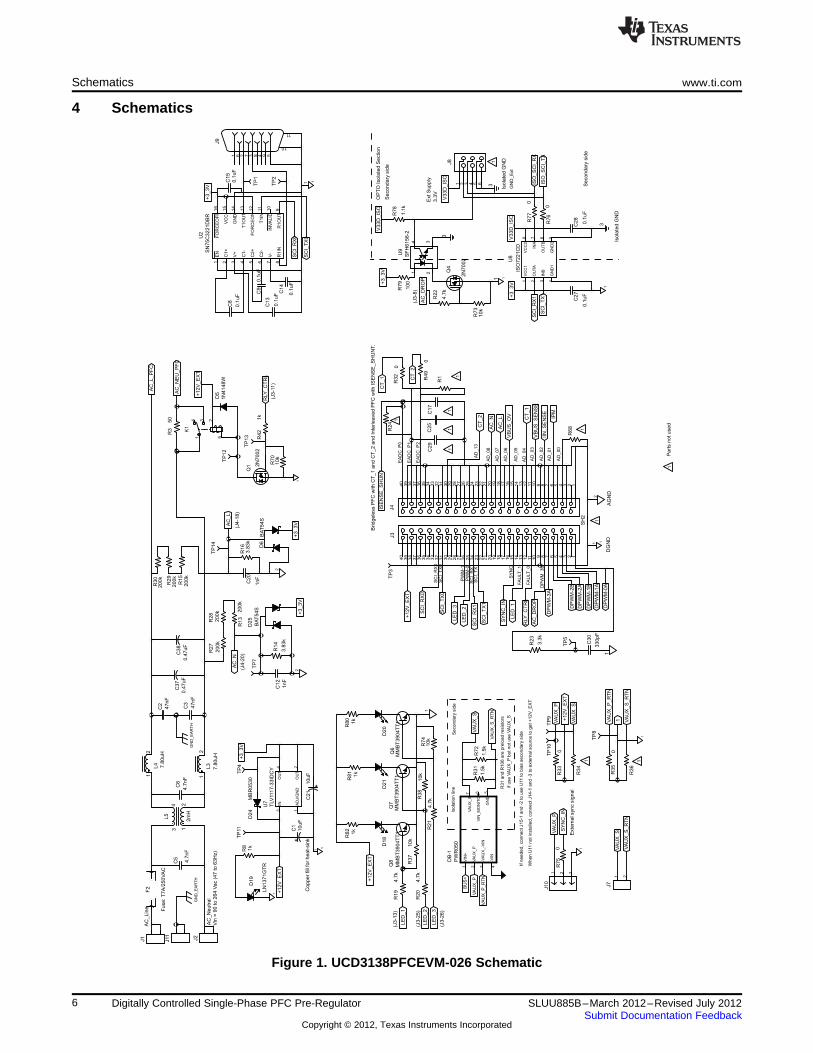
4 Schematics
Figure 1. UCD3138PFCEVM-026 Schematic
6 Digitally Controlled Single-Phase PFC Pre-Regulator SLUU885B–March 2012–Revised July 2012Submit Documentation Feedback
Copyright © 2012, Texas Instruments Incorporated
Inte
rleaved P
FC
: Jum
p a
cro
ss E
6 a
nd E
4, and E
1 a
nd E
5.
PG
ND
Bridgele
ss P
FC
: Jum
p a
cro
ss E
2 a
nd E
6, and E
3 a
nd E
1.
Vbus =
390V
DC
, Io
ut =
0.9
2A
DG
ND
31
31
1
1
1
1 1
1
Pa
rts n
ot
use
d1
1
Sin
gle
-phase P
FC
: defa
ult c
onnection E
6 to E
4.
1 1
1
1
1 1
(J4-4
0)
(J3-1
5)
(J3-7
)
+ -Vbus
(J4-1
0)
(J4-1
6)
(J4-3
0)
(J3-3
)
(J3-4
)
(J3-5
)
(J3-6
)
(J4-1
2)
(J4-8
)
(J4-6
)
TP
23
TP
22
TP
24
TP
20
C18
0.1
uF
TP
16
R71
910
SH
1
R60
49.9
k
TP
21
E3
E2R
48
1.8
k
C7
4.7
nF
E4
E5
E1
E6
C32
150pF
R44
0
R43
R66
15
TP
19
R64
10k
R55
5.2
3
TP
26
D3
BA
T54SD
14
C3D
10060G
D13
C3D
10060G
R50
1.8
k
C24
0.1
uF
TP
17
C40
47nF
C19
0.1
uF
R9
100k
TP
15
R10
100k
J6
+C
34
220uF
R4
5.0
1k
C23
0.1
uF
TP
6
R40
C26
1uF
TP
25
HS
3
C39
47nF
R47
1.8
k
R25
100k
D4
BA
T54S
R69
1.6
k
C36
100pF
R39
2k
C16
0.0
1uF
R6
0.0
2
R7
0.0
2C
22
47nF
TP
18
R18
100k
R17
100k
R11
100k
D2
BA
T54S
R45
100
D7
MU
RS
160T
3
R63
15
D15
BA
T54S
R53
5.2
3
D22
BA
T54S
D11
MB
R0530
L1
327uH
C33
47nF
R46
100k
R67
100k
R59
49.9
k
U3
OP
A350E
A
D8
BA
T54C
R2
3.3
M
R58
2k
D23
BA
T54S
R12
100k
D16
6A
6-T
1N
/C
2IN
A
3G
ND
4IN
B5
OU
TB
6V
DD
7O
UTA
8N
/C
U4
UC
C27324D
R65
10k
HS
2
Q2
IPP60R199CP
8 731
T2
PA
1005.0
50
+C
31
47uFL
2
327uH
Q3
IPP
60R
199C
P
873 1
T1
PA
1005.0
50
R26
100k
R51
100k
R62
100k
C41
47nF
D1
BA
T54S
C35
100pF
D12
MB
R0530
2 36
4
7
U1
OP
A350E
A
Q5
2N
7002
D17
GB
U8J
C4
0.1
uF
VD
D
GN
D
IN+
IN-
OU
T
U5
VD
D
GN
D
IN+
IN-
OU
T
U6
C10
C11
D9
ZH
CS
506
D10
ZH
CS
506
J5
HS
1
12
JM
P1
R61
1k
R5 1k
R54 0
R41
0
R52
0
R56
10k
R57
10k
1
1
AC
_L_P
FC
+3_3V
IIN
_S
EN
SE
IPM
DP
WM
-3A
SY
NC
_IN
+3_3V
CT
_2
DP
WM
-1B
DP
WM
-1A
CT
_1
SW
ITC
H_
NO
DE
+3_3V
AC
_N
EU
_P
FC
+3_3V
DP
WM
-2A
DP
WM
-2B
+3_3V
+3_3V
+3_3V
SW
ITC
H_
NO
DE
+3_3V
VB
US
_S
EN
SE
ISE
NS
E_S
HU
NT
+12V
_E
XT
VB
US
_O
V+
12V
_E
XT
+12V
_E
XT
2
2
2
2
2
22
2
2
2
GN
D_E
AR
TH
BU
S+
1
1
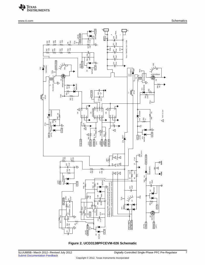
www.ti.com Schematics
Figure 2. UCD3138PFCEVM-026 Schematic
7SLUU885B–March 2012–Revised July 2012 Digitally Controlled Single-Phase PFC Pre-RegulatorSubmit Documentation Feedback
Copyright © 2012, Texas Instruments Incorporated
Electronic
LoadVM1
+
AC Source
J6 J5
TP17TP22
J1 J2
L N
Test Setup www.ti.com
5 Test Setup
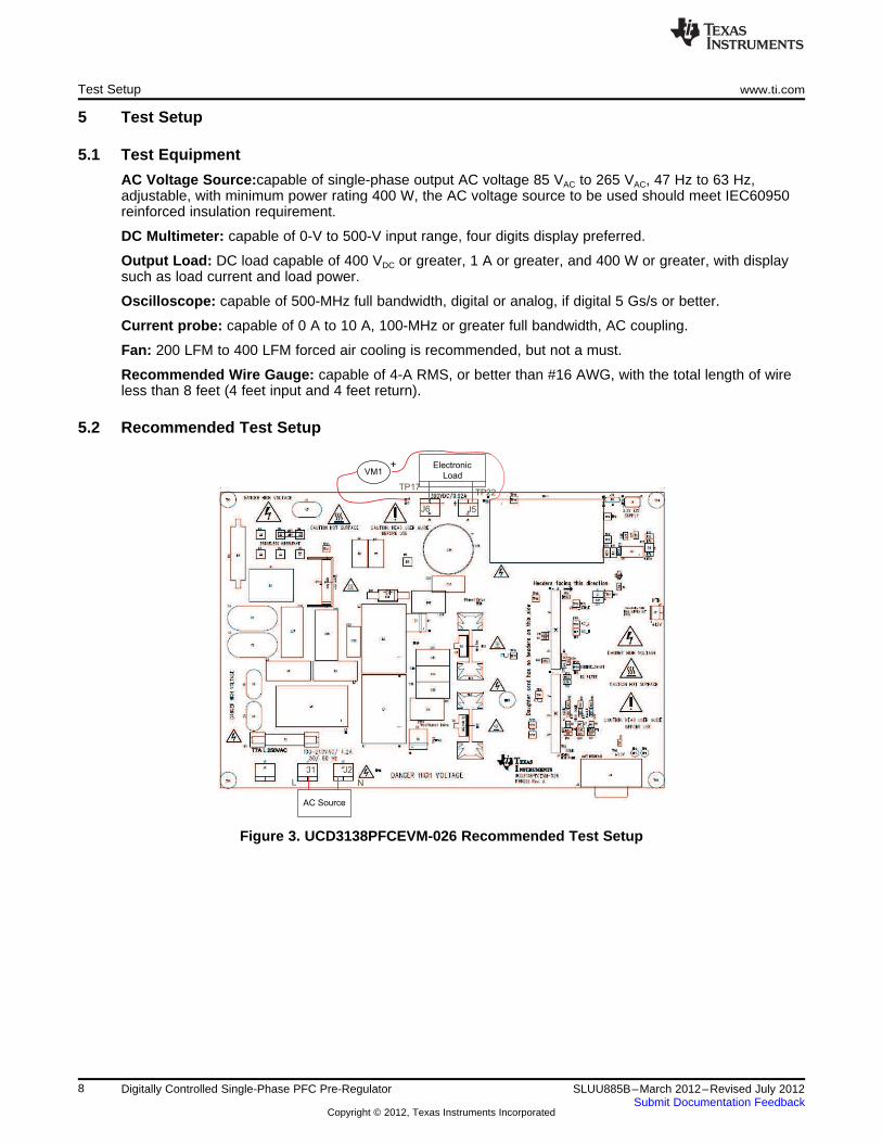
5.1 Test Equipment
AC Voltage Source:capable of single-phase output AC voltage 85 VAC to 265 VAC, 47 Hz to 63 Hz,adjustable, with minimum power rating 400 W, the AC voltage source to be used should meet IEC60950reinforced insulation requirement.
DC Multimeter: capable of 0-V to 500-V input range, four digits display preferred.
Output Load: DC load capable of 400 VDC or greater, 1 A or greater, and 400 W or greater, with displaysuch as load current and load power.
Oscilloscope: capable of 500-MHz full bandwidth, digital or analog, if digital 5 Gs/s or better.
Current probe: capable of 0 A to 10 A, 100-MHz or greater full bandwidth, AC coupling.
Fan: 200 LFM to 400 LFM forced air cooling is recommended, but not a must.
Recommended Wire Gauge: capable of 4-A RMS, or better than #16 AWG, with the total length of wireless than 8 feet (4 feet input and 4 feet return).
5.2 Recommended Test Setup
Figure 3. UCD3138PFCEVM-026 Recommended Test Setup
8 Digitally Controlled Single-Phase PFC Pre-Regulator SLUU885B–March 2012–Revised July 2012Submit Documentation Feedback
Copyright © 2012, Texas Instruments Incorporated
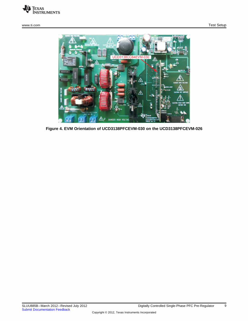
UCD3138CC64EVM-030
www.ti.com Test Setup
Figure 4. EVM Orientation of UCD3138PFCEVM-030 on the UCD3138PFCEVM-026
9SLUU885B–March 2012–Revised July 2012 Digitally Controlled Single-Phase PFC Pre-RegulatorSubmit Documentation Feedback
Copyright © 2012, Texas Instruments Incorporated
List of Test Points www.ti.com
6 List of Test Points
Table 2. List of Test Points
TEST POINTS NAME DESCRIPTION
TP1 T1OUT UART0 (J9-2) T1OUT
TP2 R1IN UART0 (J9-3) R1IN
TP3 DGND Digital GND of J3 connection
TP4 +3_3V 3.3-V LDO output on board from 12 V
TP5 RC-PWM-0A DPWM0A RC filter
TP6 CT_2 Second phase current sensing signal
TP7 AC_N Input voltage sensing signal of Neutral wire
TP8 DGND Digital GND and same as TP3
TP9 VAUX_S Secondary side 12 V on board. Not used, but can be used for external circuit.
TP10 VAUX_P 12-V output on board from DB-1, UCC28600EVM400V-12V
TP11 +12V_EXT 12 V on board from VAUX_P
TP12 K1 Relay K1 coil
TP14 AC_L Input sensing signal of Line wire
TP15 VBUS_SENSE PFC output voltage sensing signal
TP16 GND Analog GND
TP17 BUS- PFC output return
TP18 REC-1 Rectifier positive output
TP19 CT-1 Current sensing signal from current transformer T1
TP20 ISENSE Current sensing signal after conditioning
TP21 REC-2 Rectifier return
TP22 BUS+ PFC output positive, nominal 390VDC
TP23 SW2 Q2 Drain pin
TP24 SW1 Q3 Drain pin
TP25 Q2-Gate Gate pin of Q2 MOSFET
TP26 Q3-Gate Gate pin of Q3 MOSFET
7 List of Terminals
Table 3. List of Terminals
TERMINAL NAME DESCRIPTION
J1 Line Board AC input line, single-pin connection – screw type, J1 and J2 are AC input terminals,rated up to 264 VAC and maximum 7.5 A, 47 Hz to 63 Hz.
J2 Neutral Board AC input neutral, single-pin connection – screw type
J3 DJ Digital signal connection, 40 pins
J4 AJ Analog signal connection, 40 pins
J5 BUS+ PFC output positive connection, single-pin connection – screw type, BUS+ and BUS- are DCoutput terminals, rated maximum 400 VDC, and maximum current 1 A.
J6 BUS- PFC output return, single-pin connection – screw type
J7 12V_Sec 12-V auxiliary to supply to external circuit on the secondary side, 2 pins
J8 UART1 Isolated and communication to DC converter, not production tested, 6 pins
J9 UART0 Non-isolated connection, standard RS232, 9 pins,
J10 Sync External 12-V bias and sync signal, 3 pins
J11 Chassis Chassis ground, or earth connection, single-pin connection – screw type
10 Digitally Controlled Single-Phase PFC Pre-Regulator SLUU885B–March 2012–Revised July 2012Submit Documentation Feedback
Copyright © 2012, Texas Instruments Incorporated

www.ti.com Test Procedure
8 Test Procedure
8.1 Efficiency Measurement Procedure1. Refer to Figure 3 for basic setup to measure power conversion efficiency. The required equipment to
do this measurement is listed in Section 5.1.
2. Before making electrical connections, visually check the boards to make sure there are no suspectedspots of damages.
3. In this EVM package, three EVMs are included, UCD3138PFCEVM-026, UCD3138CC64EVM-030,and USB-TO-GPIO. In this measurement, the board of UCD3138PFCEVM-026 andUCD3138CC64EVM-030 is needed.
4. First install the board of UCD3138CC64EVM-030 onto the board of UCD3138PFCEVM-026. Care mustbe given to the alignment and the orientation of two boards, or damage may occur. Refer to Figure 4for UCD3138CC64EVM-030 board orientation.
5. Connect the AC voltage source to J1 (Line) and J2 (Neutral). The AC voltage source should be anisolated one and meet IEC60950 requirement. Set up the AC output voltage in the range specified inTable 1, between 90 VAC and 264 VAC, between 47 Hz and 63 Hz; set up the AC source current limit to7.5-A peak and RMS, respectively.
6. Connect an electronic load with either constant current mode or constant resistance mode. The loadrange is from 0 A to 0.92 A. Initial power on is recommended with 0-A load current. The load isrequired to receive 0 VDC to 500 VDC.
7. If the load does not have a current or a power display, a current meter is needed to insert into betweenthe load and the board.
8. Connect a volt-meter across the load and set up the volt-meter scale 0 V to 500 V on its voltage, DC.
9. Turn on the AC voltage output and varying the load. Then the measurement can be made.
WARNINGDanger of Electrical Shock! High voltage present during themeasurement!
Danger of Heat Burn from High Temperature!
Do not leave EVM powered when unattended!
8.2 Equipment Shutdown1. Shut down AC voltage source.
2. Shut down electronic load.
11SLUU885B–March 2012–Revised July 2012 Digitally Controlled Single-Phase PFC Pre-RegulatorSubmit Documentation Feedback
Copyright © 2012, Texas Instruments Incorporated
0.900
0.950
1.000
1.050
0.1 0.3 0.5 0.7 0.9Load Current (A)
115VAC 60Hz
230VAC 50Hz
80.0%
85.0%
90.0%
95.0%
0.1 0.3 0.5 0.7 0.9Load Current (A)
115VAC 60Hz
230VAC 50Hz
Performance Data and Typical Characteristic Curves www.ti.com
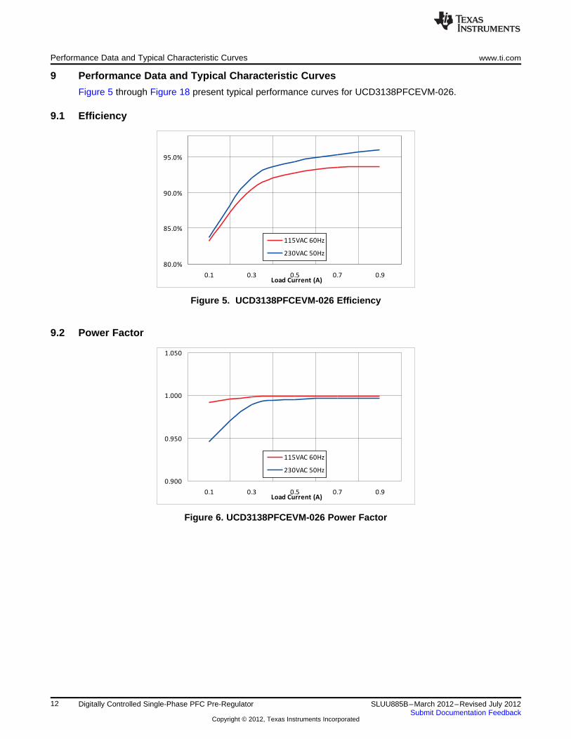
9 Performance Data and Typical Characteristic Curves
Figure 5 through Figure 18 present typical performance curves for UCD3138PFCEVM-026.
9.1 Efficiency
Figure 5. UCD3138PFCEVM-026 Efficiency
9.2 Power Factor
Figure 6. UCD3138PFCEVM-026 Power Factor
12 Digitally Controlled Single-Phase PFC Pre-Regulator SLUU885B–March 2012–Revised July 2012Submit Documentation Feedback
Copyright © 2012, Texas Instruments Incorporated
1.000%
6.000%
11.000%
0.1 0.3 0.5 0.7 0.9Load Current (A)
115VAC 60Hz
230VAC 50Hz
www.ti.com Performance Data and Typical Characteristic Curves
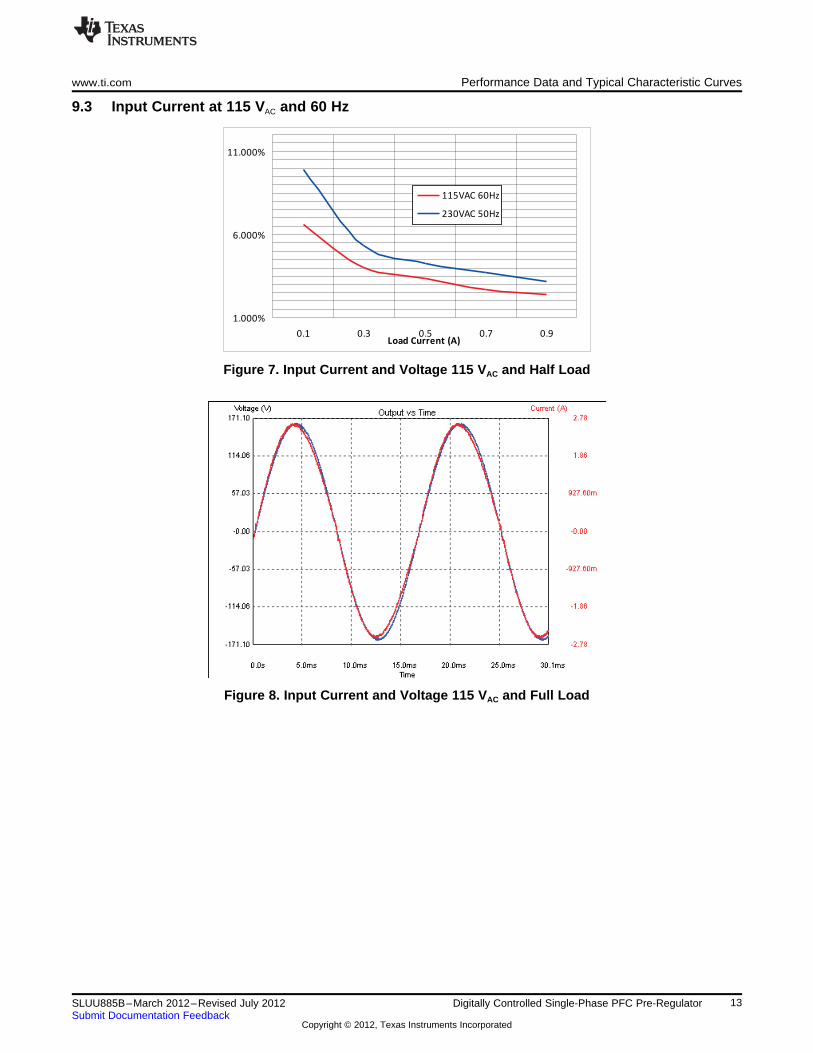
9.3 Input Current at 115 VAC and 60 Hz
Figure 7. Input Current and Voltage 115 VAC and Half Load
Figure 8. Input Current and Voltage 115 VAC and Full Load
13SLUU885B–March 2012–Revised July 2012 Digitally Controlled Single-Phase PFC Pre-RegulatorSubmit Documentation Feedback
Copyright © 2012, Texas Instruments Incorporated
Performance Data and Typical Characteristic Curves www.ti.com
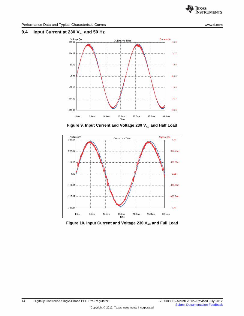
9.4 Input Current at 230 VAC and 50 Hz
Figure 9. Input Current and Voltage 230 VAC and Half Load
Figure 10. Input Current and Voltage 230 VAC and Full Load
14 Digitally Controlled Single-Phase PFC Pre-Regulator SLUU885B–March 2012–Revised July 2012Submit Documentation Feedback
Copyright © 2012, Texas Instruments Incorporated
www.ti.com Performance Data and Typical Characteristic Curves
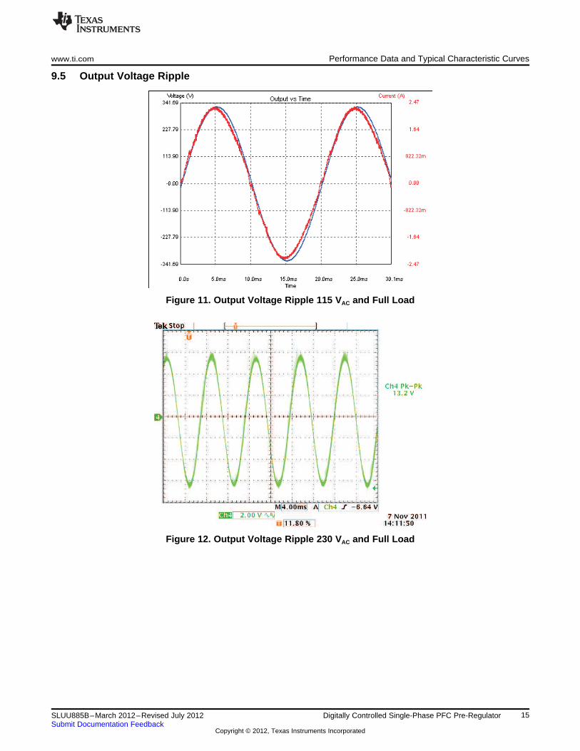
9.5 Output Voltage Ripple
Figure 11. Output Voltage Ripple 115 VAC and Full Load
Figure 12. Output Voltage Ripple 230 VAC and Full Load
15SLUU885B–March 2012–Revised July 2012 Digitally Controlled Single-Phase PFC Pre-RegulatorSubmit Documentation Feedback
Copyright © 2012, Texas Instruments Incorporated
Performance Data and Typical Characteristic Curves www.ti.com
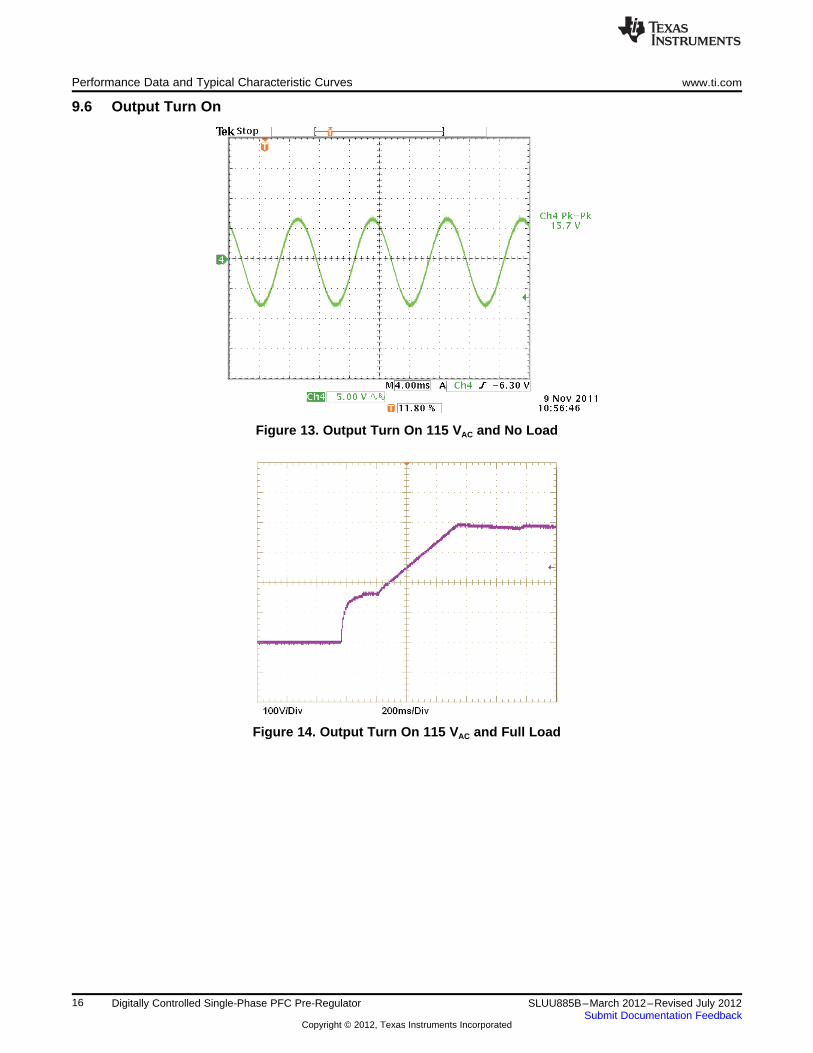
9.6 Output Turn On
Figure 13. Output Turn On 115 VAC and No Load
Figure 14. Output Turn On 115 VAC and Full Load
16 Digitally Controlled Single-Phase PFC Pre-Regulator SLUU885B–March 2012–Revised July 2012Submit Documentation Feedback
Copyright © 2012, Texas Instruments Incorporated
www.ti.com Performance Data and Typical Characteristic Curves
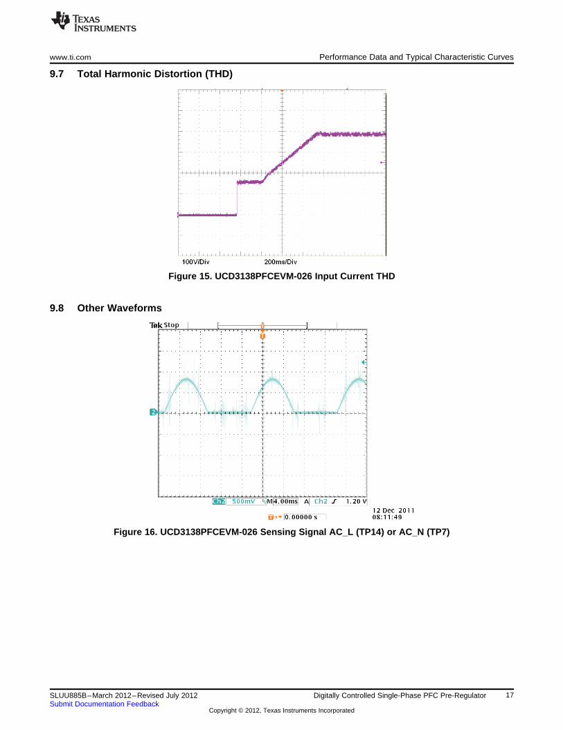
9.7 Total Harmonic Distortion (THD)
Figure 15. UCD3138PFCEVM-026 Input Current THD
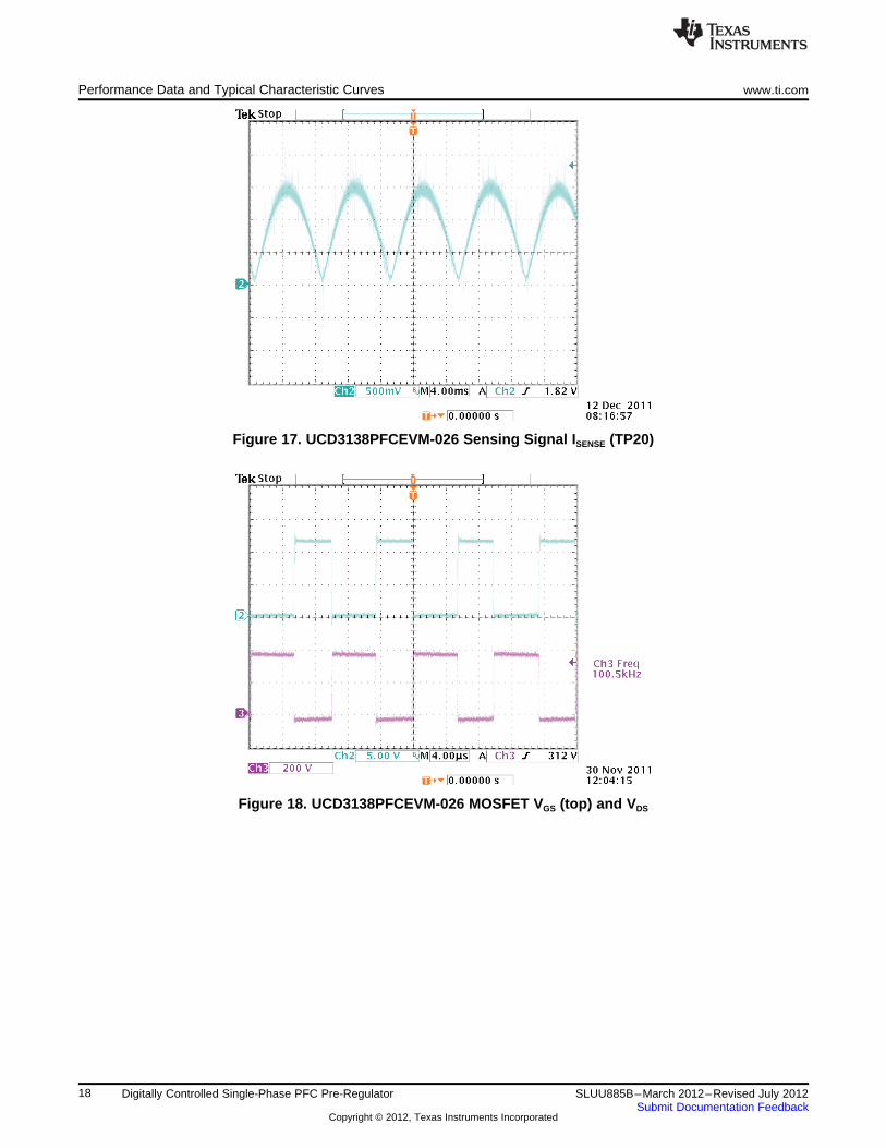
9.8 Other Waveforms
Figure 16. UCD3138PFCEVM-026 Sensing Signal AC_L (TP14) or AC_N (TP7)
17SLUU885B–March 2012–Revised July 2012 Digitally Controlled Single-Phase PFC Pre-RegulatorSubmit Documentation Feedback
Copyright © 2012, Texas Instruments Incorporated
Performance Data and Typical Characteristic Curves www.ti.com
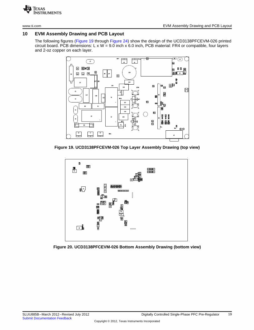
Figure 17. UCD3138PFCEVM-026 Sensing Signal ISENSE (TP20)
Figure 18. UCD3138PFCEVM-026 MOSFET VGS (top) and VDS
18 Digitally Controlled Single-Phase PFC Pre-Regulator SLUU885B–March 2012–Revised July 2012Submit Documentation Feedback
Copyright © 2012, Texas Instruments Incorporated
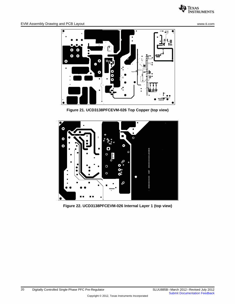
www.ti.com EVM Assembly Drawing and PCB Layout
10 EVM Assembly Drawing and PCB Layout
The following figures (Figure 19 through Figure 24) show the design of the UCD3138PFCEVM-026 printedcircuit board. PCB dimensions: L x W = 9.0 inch x 6.0 inch, PCB material: FR4 or compatible, four layersand 2-oz copper on each layer.
Figure 19. UCD3138PFCEVM-026 Top Layer Assembly Drawing (top view)
Figure 20. UCD3138PFCEVM-026 Bottom Assembly Drawing (bottom view)
19SLUU885B–March 2012–Revised July 2012 Digitally Controlled Single-Phase PFC Pre-RegulatorSubmit Documentation Feedback
Copyright © 2012, Texas Instruments Incorporated
EVM Assembly Drawing and PCB Layout www.ti.com
Figure 21. UCD3138PFCEVM-026 Top Copper (top view)
Figure 22. UCD3138PFCEVM-026 Internal Layer 1 (top view)
20 Digitally Controlled Single-Phase PFC Pre-Regulator SLUU885B–March 2012–Revised July 2012Submit Documentation Feedback
Copyright © 2012, Texas Instruments Incorporated
www.ti.com EVM Assembly Drawing and PCB Layout
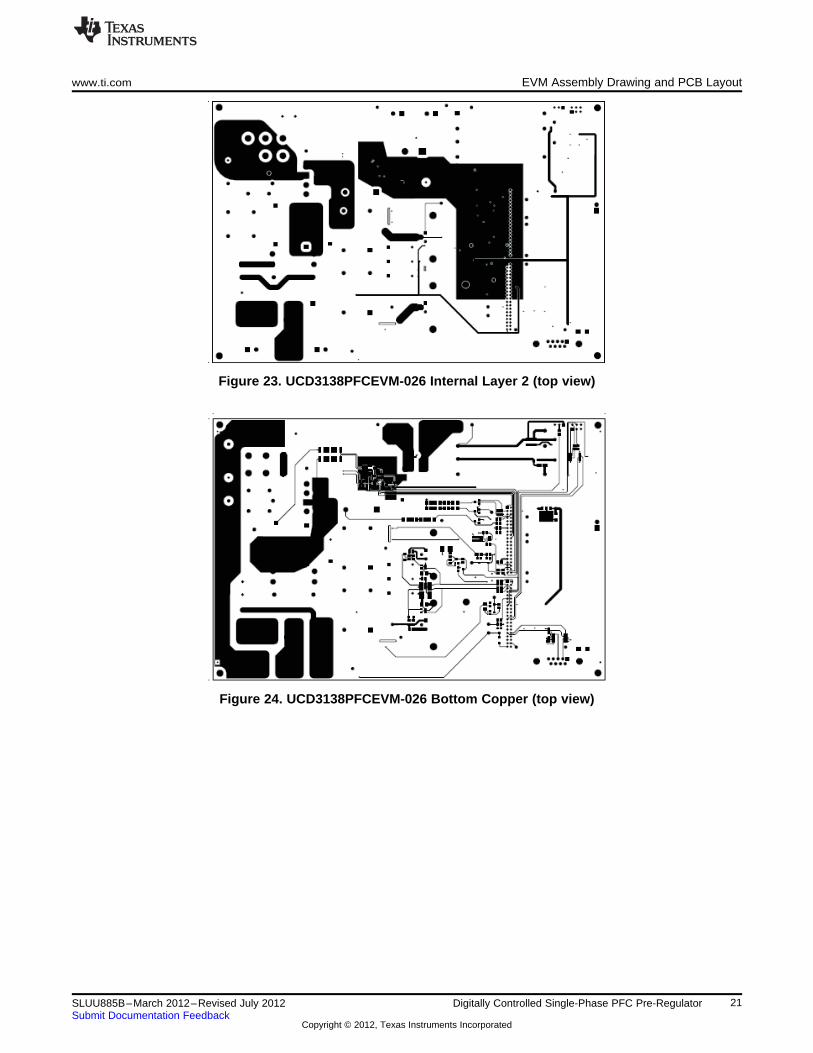
Figure 23. UCD3138PFCEVM-026 Internal Layer 2 (top view)
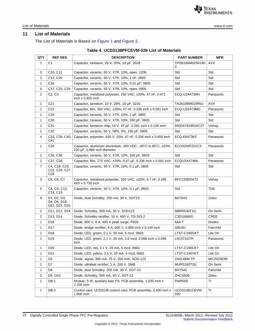
Figure 24. UCD3138PFCEVM-026 Bottom Copper (top view)
21SLUU885B–March 2012–Revised July 2012 Digitally Controlled Single-Phase PFC Pre-RegulatorSubmit Documentation Feedback
Copyright © 2012, Texas Instruments Incorporated
List of Materials www.ti.com
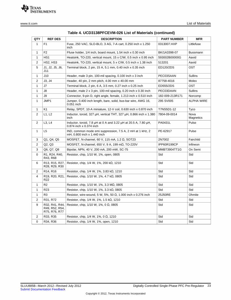
11 List of Materials
The List of Materials is Based on Figure 1 and Figure 2.
Table 4. UCD3138PFCEVM-026 List of Materials
QTY REF DES DESCRIPTION PART NUMBER MFR
1 C1 Capacitor, tantalum, 25 V, 20%, 10 µF, 3528 TPSB106M025R180 AVX0
0 C10, C11 Capacitor, ceramic, 50 V, X7R, 10%, open, 1206 Std Std
2 C12, C20 Capacitor, ceramic, 50 V, X7R, 10%, 1 nF, 0805 Std Std
1 C16 Capacitor, ceramic, 50 V, X7R, 10%, 0.01 µF, 0805 Std Std
0 C17, C25, C29 Capacitor, ceramic, 50 V, X7R, 10%, open, 0805 Std Std
2 C2, C3 Capacitor, metalized polyester, 250 VAC, ±20%, 47 nF, 0.472 ECQ-U2A473MV Panasonicinch x 0.925 inch
1 C21 Capacitor, tantalum, 10 V, 20%, 10 µF, 3216 TAJA106M010RNJ AVX
1 C22 Capacitor, film, 300 VAC, ±20%, 47 nF, 0.236 inch x 0.591 inch ECQ-U3A473MG Panasonic
1 C26 Capacitor, ceramic, 50 V, X7R, 10%, 1 µF, 0805 Std Std
1 C30 Capacitor, ceramic, 50 V, X7R, 10%, 330 pF, 0805 Std Std
1 C31 Capacitor, tantalum chip, 16 V, 47 µF, 0.281 inch x 0.126 inch 595D476X9016C2T Vishay
1 C32 Capacitor, ceramic, 50 V, NP0, 5%, 150 pF, 0805 Std Std
4 C33, C39, C40, Capacitor, polyester, 630 V, 10%, 47 nF, 0.256 inch x 0.650 inch ECQ-E6473KF PanasonicC41
1 C34 Capacitor, aluminum electrolytic, 450 VDC, -40°C to 85°C, ±20%, ECOS2WP221CX Panasonic220 µF, 0.984 inch diameter
2 C35, C36 Capacitor, ceramic, 50 V, X7R, 10%, 100 pF, 0603 Std Std
2 C37, C38 Capacitor, film, 275 VAC, ±20%, 0.47 µF, 0.236 inch x 0.591 inch ECQU2A474ML Panasonic
7 C4, C18, C19, Capacitor, ceramic, 50 V, X7R, 10%, 0.1 µF, 0805 Std StdC23, C24, C27,C28
3 C5, C6, C7 Capacitor, metalized polyester, 250 VAC, ±20%, 4.7 nF, 0.295 BFC233820472 Vishayinch x 0.730 inch
5 C8, C9, C13, Capacitor, ceramic, 50 V, X7R, 10%, 0.1 µF, 0603 Std TDKC14, C15
9 D1, D2, D3, Diode, dual Schottky, 200 mA, 30 V, SOT23 BAT54S ZetexD4, D6, D15,D22, D23, D25
2 D11, D12, D24 Diode, Schottky, 500 mA, 30 V, SOD123 MBR0530T1G On Semi
2 D13, D14 Diode, Schottky rectifier, 10 A, 600 V, TO-263-2 C3D10060G CREE
1 D16 Diode, 600 V, 6 A, 400 A peak surge, P600 6A6-T Diodes
1 D17 Diode, bridge rectifier, 8 A, 600 V, 0.880 inch x 0.140 inch GBU8J Fairchild
1 D18 Diode, LED, green, 2.1 V, 20 mA, 6 mcd, 0603 LTST-C190GKT Lite On
1 D19 Diode, LED, green, 2.1 V, 20 mA, 0.9 mcd, 0.068 inch x 0.049 LN1371GTR Panasonicinch
1 D20 Diode, LED, red, 2.1 V, 20 mA, 6 mcd, 0603 LTST-C190CKT Lite On
1 D21 Diode, LED, yellow, 2.1 V, 20 mA, 6 mcd, 0603 LTST-C190YKT Lite On
1 D5 Diode, signal, 300 mA, 75 V, 350 mW, SOD-123 1N4148W-TP MICROSEMI
1 D7 Diode, ultrafast rectifier, 1 A, 200 V, SMB MURS160T3G On Semi
1 D8 Diode, dual Schottky, 200 mA, 30 V, SOT-23 BAT54C Fairchild
2 D9, D10 Diode, Schottky, 500 mA, 60 V, SOT-23 ZHCS506 Zetex
1 DB-1 Module, 5 W, auxiliary bias PS, PCB assembly, 1.200 inch x PWR050 TI2.200 inch
1 DB-2 Control card, UCD3138 control card, PCB assembly, 3.400 inch x UCD3138CCEVM- TI1.800 inch 030
22 Digitally Controlled Single-Phase PFC Pre-Regulator SLUU885B–March 2012–Revised July 2012Submit Documentation Feedback
Copyright © 2012, Texas Instruments Incorporated
www.ti.com List of Materials
Table 4. UCD3138PFCEVM-026 List of Materials (continued)
QTY REF DES DESCRIPTION PART NUMBER MFR
1 F1 Fuse, 250 VAC, SLO-BLO, 3 AG, 7-A cart, 0.250 inch x 1.250 0313007.HXP Littlefuseinch
1 F2 Ffuse holder, 1/4 inch, board mount, 1.54 inch x 0.30 inch BK/1A3398-07 Bussmann
1 HS1 Heatsink, TO-220, vertical mount, 15 x C/W, 0.5 inch x 0.95 inch 593002B00000G Aavid
2 HS2, HS3 Heatsink, TO-220, vertical mount, 5 x C/W, 0.5 inch x 1.38 inch 513201 Aavid
5 J1, J2, J5, J6, Terminal block, 2 pin, 15 A, 5.1 mm, 0.40 inch x 0.35 inch ED120/2DS OSTJ11
1 J10 Header, male 3 pin, 100-mil spacing, 0.100 inch x 3 inch PEC03SAAN Sullins
2 J3, J4 Header, 40 pin, 2 mm pitch, 4.00 mm x 40.00 mm 87758-4016 Molex
1 J7 Terminal block, 2 pin, 6 A, 3.5 mm, 0.27 inch x 0.25 inch ED555/2DS OST
1 J8 Header, male 2 x 3 pin, 100-mil spacing, 0.20 inch x 0.30 inch PEC03DAAN Sullins
1 J9 Connector, 9-pin D, right angle, female, 1.213 inch x 0.510 inch 182-009-213R171 Norcomp
1 JMP1 Jumper, 0.400 inch length, bare, solid, bus-bar wire, AWG 16, 295 SV005 ALPHA WIRE0.051 inch
1 K1 Relay, SPDT, 10-A miniature, 12-V coil, 0.630 inch x 0.870 inch T7NS5D1-12 Tyco
2 L1, L2 Inductor, toroid, 327 µH, vertical THT, 327 µH, 0.866 inch x 1.380 7804-09-0014 Novainch Magnetics
2 L3, L4 Inductor, toroid, 7.8 µH at 0 A and 3.22 µH at 20.5 A, 7.80 µH, PA0431L Pulse0.874 inch x 0.374 inch
1 L5 IND, common mode emi suppression, 7.5 A, 2 mH at 1 kHz, 2 PE-62917 PulsemH, 0.800 inch x 1.440 inch
3 Q1, Q4, Q5 MOSFET, N-channel, 60 V, 115 mA, 1.2 Ω, SOT23 2N7002 Fairchild
2 Q2, Q3 MOSFET, N-channel, 650 V, 9 A, 199 mΩ, TO-220V IPP60R199CP Infineon
3 Q6, Q7, Q8 Bipolar, NPN, 40 V, 200 mA, 200 mW, SC-75 MMBT3904TT1G On Semi
0 R1, R24, R40, Resistor, chip, 1/10 W, 1%, open, 0805 Std StdR43, R68
6 R13, R15, R27, Resistor, chip, 1/4 W, 1%, 200 kΩ, 1210 Std StdR28, R29, R30
2 R14, R16 Resistor, chip, 1/4 W, 1%, 3.83 kΩ, 1210 Std Std
4 R19, R20, R21, Resistor, chip, 1/10 W, 1%, 4.7 kΩ, 0805 Std StdR22
1 R2 Resistor, chip, 1/10 W, 1%, 3.3 MΩ, 0805 Std Std
1 R23 Resistor, chip, 1/10 W, 1%, 3.3 kΩ, 0805 Std Std
1 R3 Resistor, wire-wound, 5 W, 5%, 50 Ω, 1.000 inch x 0.276 inch 25J50RE Ohmite
2 R31, R72 Resistor, chip, 1/4 W, 1%, 1.5 kΩ, 1210 Std Std
9 R32, R41, R44, Resistor, chip, 1/10 W, 1%, 0 Ω, 0805 Std StdR49, R52, R54,R75, R76, R77
2 R33, R35 Resistor, chip, 1/4 W, 1%, 0 Ω, 1210 Std Std
0 R34, R36 Resistor, chip, 1/4 W, 1%, open, 1210 Std Std
23SLUU885B–March 2012–Revised July 2012 Digitally Controlled Single-Phase PFC Pre-RegulatorSubmit Documentation Feedback
Copyright © 2012, Texas Instruments Incorporated
List of Materials www.ti.com
Table 4. UCD3138PFCEVM-026 List of Materials (continued)
QTY REF DES DESCRIPTION PART NUMBER MFR
7 R37, R38, R56, Resistor, chip, 1/10 W, 1%, 10 kΩ, 0805 Std StdR57, R70, R73,R74
2 R39, R58 Resistor, chip, 1/10 W, 1%, 2 kΩ, 0805 Std Std
1 R4 Resistor, chip, 1/10 W, 1%, 5.01 kΩ, 0805 Std Std
2 R45, R79 Resistor, chip, 1/10 W, 1%, 100 Ω, 0805 Std Std
3 R47, R48, R50 Resistor, chip, 1/10 W, 1%, 1.8 kΩ, 0805 Std Std
7 R5, R8, R42, Resistor, chip, 1/10 W, 1%, 1 kΩ, 0805 Std StdR61, R80, R81,R82
2 R53, R55 Resistor, chip, 1/10 W, 1%, 5.23 Ω, 0805 Std std
2 R59, R60 Resistor, chip, 1/10 W, 1%, 49.9 kΩ, 0805 Std Std
2 R6, R7 Resistor, metal strip, 2 W, 1%, 0.02 Ω, 0.49 inch x 0.10 inch WSR2R0200FEA Vishay Dale
2 R63, R66 Resistor, chip, 1/10 W, 1%, 15 Ω, 0805 Std Std
2 R64, R65 Resistor, chip, 1/10 W, 1%, 10 kΩ, 1206 Std std
1 R69 Resistor, chip, 1/10 W, 1%, 1.6 kΩ, 0805 Std Std
1 R71 Resistor, chip, 1/10 W, 1%, 910 Ω, 0805 Std Std
1 R78 Resistor, chip, 1/10 W, 1%, 1.1 kΩ, 0805 Std Std
12 R9, R10, R11, Resistor, metal film, 1/4 W, ±5%, 100 kΩ, 1206 RC1206FR- YageoR12, R17, R18, 07100KLR25, R26, R46,R51, R62, R67
2 U1, U3 High Voltage, High Current Op-Amp, MSOP-8 OPA350EA/250 TI
1 U2 RS-232 Transceivers with Auto Shutdown, SSOP-16 SN75C3221DBR TI
1 U4 High-Speed Low-Side Power MOSFET driver, SO8 UCC27324D TI
0 U5, U6 4-A Single Channel High-Speed Low-Side Gate Drivers, open, UCC27517DBV TISOT23-6
1 U7 3.3-V, 800-mA LDO Voltage Regulators, SOT-223 TLV1117-33IDCY TI
1 U8 Digital Isolators, xx Mbps, SO-8 ISO7221CD TI
1 U9 Opto-coupler, SMD-4P SFH6156-2 Vishay
24 Digitally Controlled Single-Phase PFC Pre-Regulator SLUU885B–March 2012–Revised July 2012Submit Documentation Feedback
Copyright © 2012, Texas Instruments Incorporated
Vs
RL
Vbus
Q1
D1
Cb
SignalConditioning
Rs1
EMI Filter& Inrush
Relay
GateDriver
L1Iin D2
SignalConditioning
SignalConditioning
Vin
Iq1
DPWM 1B
Vin_L Vbus_senI_shunt
Vin_N Vbus_ov
Single-phase PFC
Circuit Diagram
SignalConditioning
I_CT1
www.ti.com Digital PFC Description
12 Digital PFC Description
12.1 1PFC Block Diagram
12.1.1 Single-Phase PFC Block Diagram
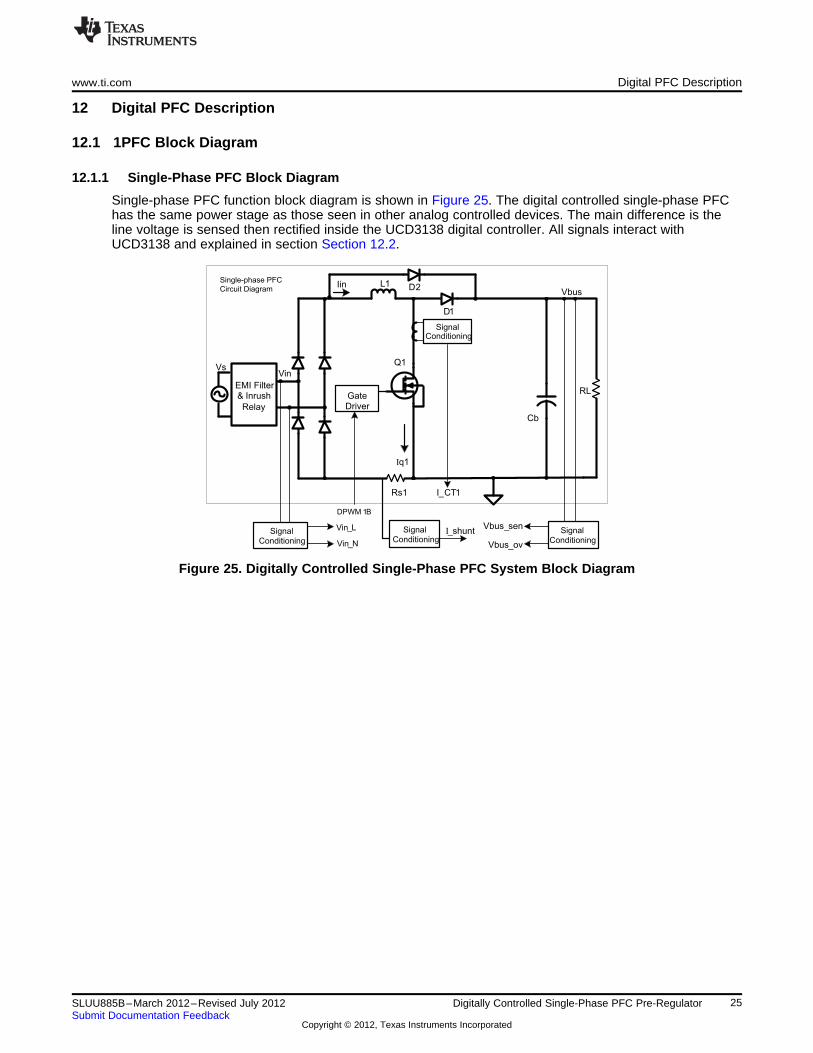
Single-phase PFC function block diagram is shown in Figure 25. The digital controlled single-phase PFChas the same power stage as those seen in other analog controlled devices. The main difference is theline voltage is sensed then rectified inside the UCD3138 digital controller. All signals interact withUCD3138 and explained in section Section 12.2.
Figure 25. Digitally Controlled Single-Phase PFC System Block Diagram
25SLUU885B–March 2012–Revised July 2012 Digitally Controlled Single-Phase PFC Pre-RegulatorSubmit Documentation Feedback
Copyright © 2012, Texas Instruments Incorporated
Vs
RL
Vbus
Q1
D1
Cb
Rs1
EMI Filter& Inrush
Relay
GateDriver
L1Iin
L2 D2
Q2
SignalConditioning
SignalConditioning
Vin
SignalConditioning
SignalConditioning
I_CT1 I_CT2DPWM1B DPWM2B
Vin_l Vbus_sen
Vin_n Vbus_ov
Vs
RL
Vbus
Q1
D1
Cb
SignalConditioning
Rs1
EMI Filter& Inrush
Relay
GateDriver
L1Iin
L2 D2
Q2
D3
SignalConditioning
SignalConditioning
Vin
Iq1Iq2
SignalConditioning
SignalConditioning
I_CT1 I_CT2DPWM1 B DPWM 2B
Vin_l Vbus_senI_shunt
Vin_n Vbus_ov
Digital PFC Description www.ti.com
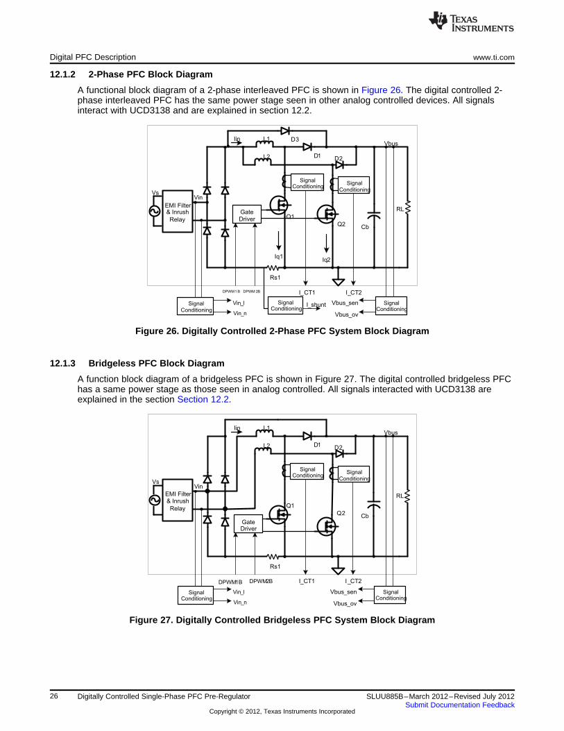
12.1.2 2-Phase PFC Block Diagram
A functional block diagram of a 2-phase interleaved PFC is shown in Figure 26. The digital controlled 2-phase interleaved PFC has the same power stage seen in other analog controlled devices. All signalsinteract with UCD3138 and are explained in section 12.2.
Figure 26. Digitally Controlled 2-Phase PFC System Block Diagram
12.1.3 Bridgeless PFC Block Diagram
A function block diagram of a bridgeless PFC is shown in Figure 27. The digital controlled bridgeless PFChas a same power stage as those seen in analog controlled. All signals interacted with UCD3138 areexplained in the section Section 12.2.
Figure 27. Digitally Controlled Bridgeless PFC System Block Diagram
26 Digitally Controlled Single-Phase PFC Pre-Regulator SLUU885B–March 2012–Revised July 2012Submit Documentation Feedback
Copyright © 2012, Texas Instruments Incorporated
Fusion Power Peripheral
AD_03
AD_07
DPWM1
PI(Gv)+ +
-
-
UCD3138
Vref
Vb
Ev
Iin
CLA1
(Gc)
Calculate
Vrms
Calculate
1/Vrms2
Iref
A
B
cUi
Vrms Conditioning&
Rectification
Km
FE0
DPWM1B
Vbus_sen
Vin_N
I_shuntEAP0
UARTInterface
Vin_L
AD_08
Cycle by cycle limit
Vbus_ovCOMP_FOVP
PMBusInterface
Single-phase PFCConfiguration
COMP_D I_CT1
www.ti.com Digital PFC Description
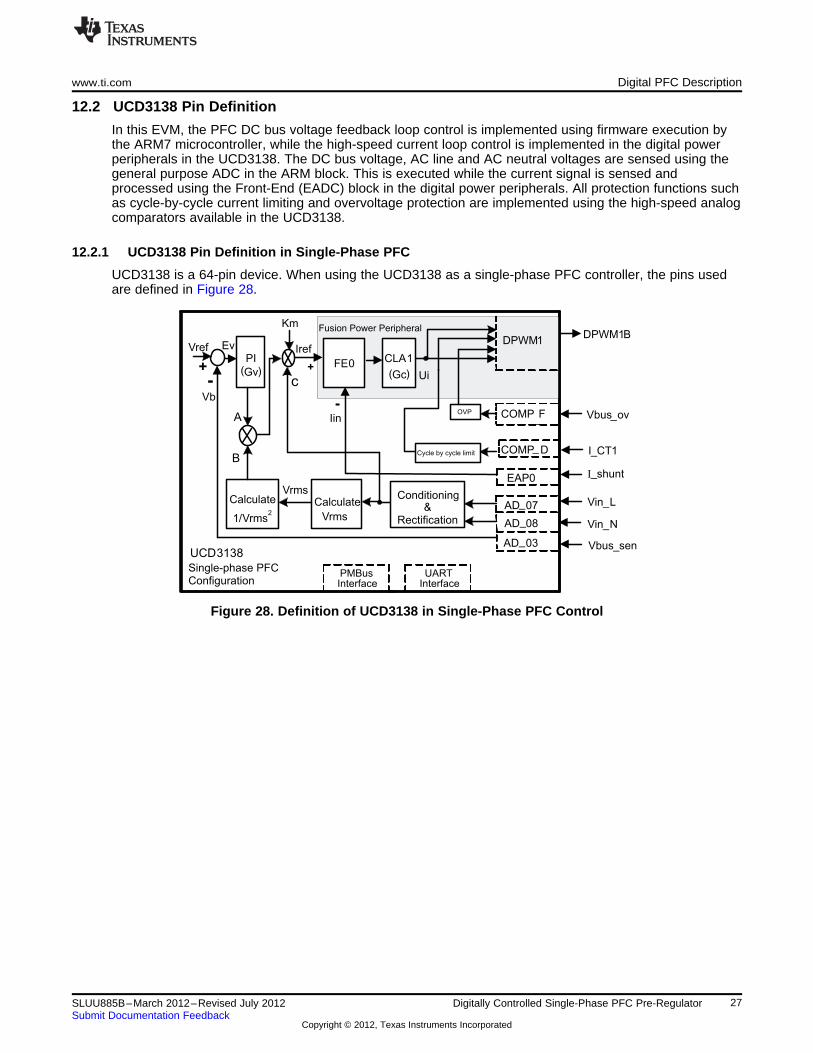
12.2 UCD3138 Pin Definition
In this EVM, the PFC DC bus voltage feedback loop control is implemented using firmware execution bythe ARM7 microcontroller, while the high-speed current loop control is implemented in the digital powerperipherals in the UCD3138. The DC bus voltage, AC line and AC neutral voltages are sensed using thegeneral purpose ADC in the ARM block. This is executed while the current signal is sensed andprocessed using the Front-End (EADC) block in the digital power peripherals. All protection functions suchas cycle-by-cycle current limiting and overvoltage protection are implemented using the high-speed analogcomparators available in the UCD3138.
12.2.1 UCD3138 Pin Definition in Single-Phase PFC
UCD3138 is a 64-pin device. When using the UCD3138 as a single-phase PFC controller, the pins usedare defined in Figure 28.
Figure 28. Definition of UCD3138 in Single-Phase PFC Control
27SLUU885B–March 2012–Revised July 2012 Digitally Controlled Single-Phase PFC Pre-RegulatorSubmit Documentation Feedback
Copyright © 2012, Texas Instruments Incorporated
Fusion Power Peripheral
DPWM2
AD_08
COMP_E
COMP_D
EAP1
DPWM1
PI
(Gv)+ +
-
-
UCD 3138
Vref
Vb
Ev
Iin
CLA1
(Gc)
CalculateVrms
Calculate
1/Vrms2
Iref
A
B
c
Cycle by cycle limit
Ui
Vrms
Conditioning&
Rectification
KmDPWM1B
DPWM2B
Vbus_sen
Vin_n
I_CT1
I_CT2EAP2
UARTInterface
Vin_lAD_07
Cycle by cycle limit
Vbus_ov
AD_03
COMP_FOVP
PMBusInterface
FE1
FE2
-
I_CT2
I_CT1
Iin
Bridgeless PFCConfiguration
Fusion Power Peripheral
DPWM2
AD_03
COMP_E
COMP_D
AD_07
DPWM1
PI
(Gv)++
-
-
UCD 3138
Vref
Vb
Ev
Iin
CLA1
(Gc)
Calculate
Vrms
Calculate
1/Vrms2
Iref
A
B
c
Cycle by cycle limit
Ui
VrmsConditioning
&Rectification
Km
FE0
DPWM1B
DPWM2B
Vbus_sen
Vin_n
I_CT1
I_CT2
I_shuntEAP0
UARTInterface
Vin_l
AD_08
Cycle by cycle limit
Vbus_ovCOMP_FOVP
PMBusInterface
2-phase interleavedPFCConfiguration
Digital PFC Description www.ti.com
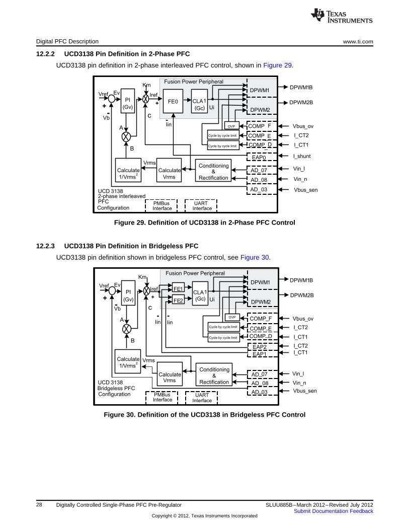
12.2.2 UCD3138 Pin Definition in 2-Phase PFC
UCD3138 pin definition in 2-phase interleaved PFC control, shown in Figure 29.
Figure 29. Definition of UCD3138 in 2-Phase PFC Control
12.2.3 UCD3138 Pin Definition in Bridgeless PFC
UCD3138 pin definition shown in bridgeless PFC control, see Figure 30.
Figure 30. Definition of the UCD3138 in Bridgeless PFC Control
28 Digitally Controlled Single-Phase PFC Pre-Regulator SLUU885B–March 2012–Revised July 2012Submit Documentation Feedback
Copyright © 2012, Texas Instruments Incorporated
www.ti.com Digital PFC Description
12.3 EVM Hardware – Introduction
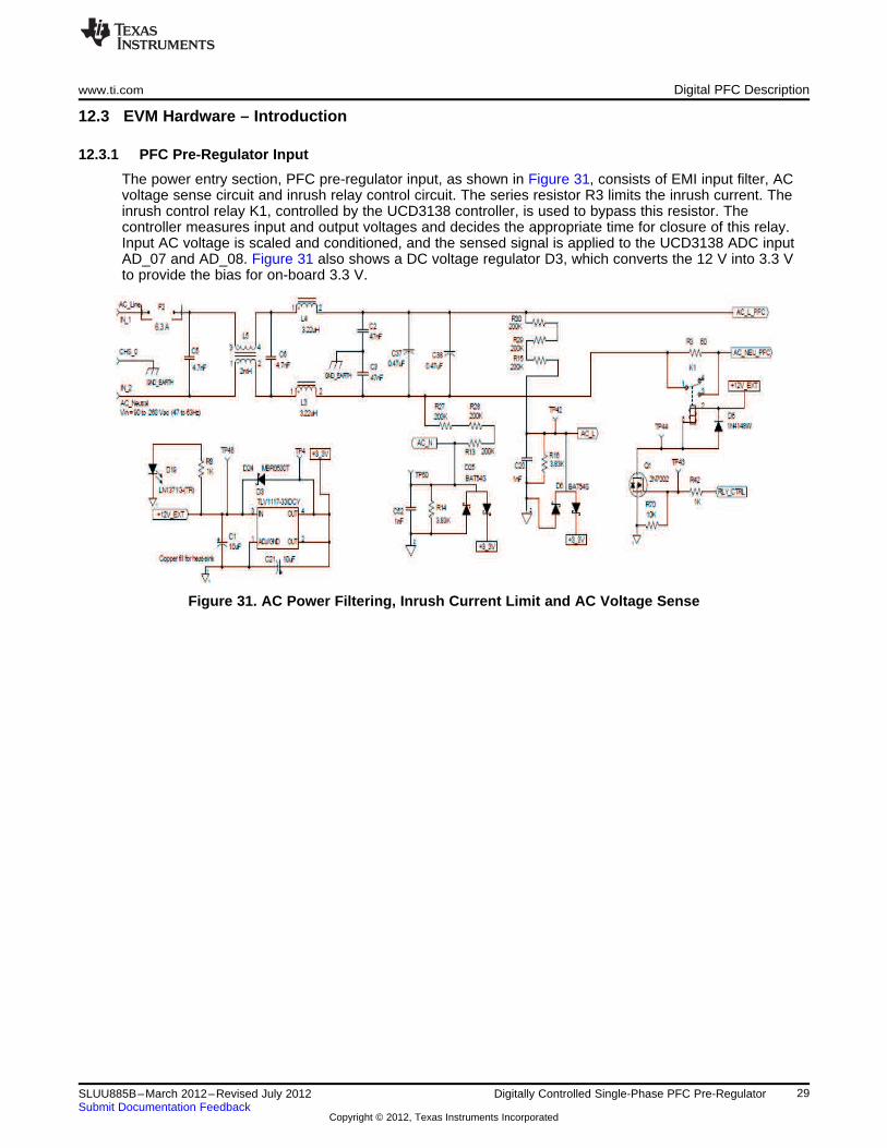
12.3.1 PFC Pre-Regulator Input
The power entry section, PFC pre-regulator input, as shown in Figure 31, consists of EMI input filter, ACvoltage sense circuit and inrush relay control circuit. The series resistor R3 limits the inrush current. Theinrush control relay K1, controlled by the UCD3138 controller, is used to bypass this resistor. Thecontroller measures input and output voltages and decides the appropriate time for closure of this relay.Input AC voltage is scaled and conditioned, and the sensed signal is applied to the UCD3138 ADC inputAD_07 and AD_08. Figure 31 also shows a DC voltage regulator D3, which converts the 12 V into 3.3 Vto provide the bias for on-board 3.3 V.
Figure 31. AC Power Filtering, Inrush Current Limit and AC Voltage Sense
29SLUU885B–March 2012–Revised July 2012 Digitally Controlled Single-Phase PFC Pre-RegulatorSubmit Documentation Feedback
Copyright © 2012, Texas Instruments Incorporated
Digital PFC Description www.ti.com
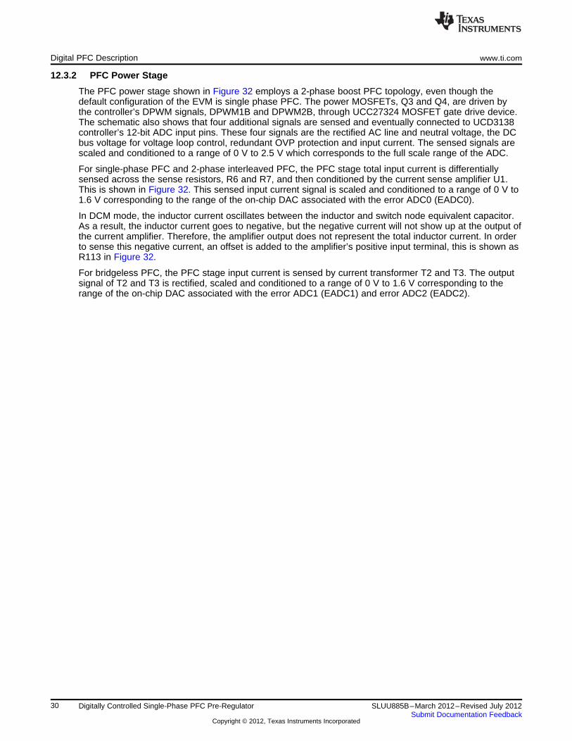
12.3.2 PFC Power Stage
The PFC power stage shown in Figure 32 employs a 2-phase boost PFC topology, even though thedefault configuration of the EVM is single phase PFC. The power MOSFETs, Q3 and Q4, are driven bythe controller’s DPWM signals, DPWM1B and DPWM2B, through UCC27324 MOSFET gate drive device.The schematic also shows that four additional signals are sensed and eventually connected to UCD3138controller’s 12-bit ADC input pins. These four signals are the rectified AC line and neutral voltage, the DCbus voltage for voltage loop control, redundant OVP protection and input current. The sensed signals arescaled and conditioned to a range of 0 V to 2.5 V which corresponds to the full scale range of the ADC.
For single-phase PFC and 2-phase interleaved PFC, the PFC stage total input current is differentiallysensed across the sense resistors, R6 and R7, and then conditioned by the current sense amplifier U1.This is shown in Figure 32. This sensed input current signal is scaled and conditioned to a range of 0 V to1.6 V corresponding to the range of the on-chip DAC associated with the error ADC0 (EADC0).
In DCM mode, the inductor current oscillates between the inductor and switch node equivalent capacitor.As a result, the inductor current goes to negative, but the negative current will not show up at the output ofthe current amplifier. Therefore, the amplifier output does not represent the total inductor current. In orderto sense this negative current, an offset is added to the amplifier’s positive input terminal, this is shown asR113 in Figure 32.
For bridgeless PFC, the PFC stage input current is sensed by current transformer T2 and T3. The outputsignal of T2 and T3 is rectified, scaled and conditioned to a range of 0 V to 1.6 V corresponding to therange of the on-chip DAC associated with the error ADC1 (EADC1) and error ADC2 (EADC2).
30 Digitally Controlled Single-Phase PFC Pre-Regulator SLUU885B–March 2012–Revised July 2012Submit Documentation Feedback
Copyright © 2012, Texas Instruments Incorporated
Inte
rleaved P
FC
: Jum
p a
cro
ss E
6 a
nd E
4, and E
1 a
nd E
5.
PG
ND
Bridgele
ss P
FC
: Jum
p a
cro
ss E
2 a
nd E
6, and E
3 a
nd E
1.
Vbus =
390V
DC
, Io
ut =
0.9
2A
DG
ND
31
31
1
1
1
1 1
1
Pa
rts n
ot
use
d1
1
Sin
gle
-phase P
FC
: defa
ult c
onnection E
6 to E
4.
1 1
1
1
1 1
(J4-4
0)
(J3-1
5)
(J3-7
)
+ -Vbus
(J4-1
0)
(J4-1
6)
(J4-3
0)
(J3-3
)
(J3-4
)
(J3-5
)
(J3-6
)
(J4-1
2)
(J4-8
)
(J4-6
)
TP
23
TP
22
TP
24
TP
20
C18
0.1
uF
TP
16
R71
910
SH
1
R60
49.9
k
TP
21
E3
E2R
48
1.8
k
C7
4.7
nF
E4
E5
E1
E6
C32
150pF
R44
0
R43
R66
15
TP
19
R64
10k
R55
5.2
3
TP
26
D3
BA
T54SD
14
C3D
10060G
D13
C3D
10060G
R50
1.8
k
C24
0.1
uF
TP
17
C40
47nF
C19
0.1
uF
R9
100k
TP
15
R10
100k
J6
+C
34
220uF
R4
5.0
1k
C23
0.1
uF
TP
6
R40
C26
1uF
TP
25
HS
3
C39
47nF
R47
1.8
k
R25
100k
D4
BA
T54S
R69
1.6
k
C36
100pF
R39
2k
C16
0.0
1uF
R6
0.0
2
R7
0.0
2C
22
47nF
TP
18
R18
100k
R17
100k
R11
100k
D2
BA
T54S
R45
100
D7
MU
RS
160T
3
R63
15
D15
BA
T54S
R53
5.2
3
D22
BA
T54S
D11
MB
R0530
L1
327uH
C33
47nF
R46
100k
R67
100k
R59
49.9
k
U3
OP
A350E
A
D8
BA
T54C
R2
3.3
M
R58
2k
D23
BA
T54S
R12
100k
D16
6A
6-T
1N
/C
2IN
A
3G
ND
4IN
B5
OU
TB
6V
DD
7O
UTA
8N
/C
U4
UC
C27324D
R65
10k
HS
2
Q2
IPP60R199CP
8 731
T2
PA
1005.0
50
+C
31
47uFL
2
327uH
Q3
IPP
60R
199C
P
873 1
T1
PA
1005.0
50
R26
100k
R51
100k
R62
100k
C41
47nF
D1
BA
T54S
C35
100pF
D12
MB
R0530
2 36
4
7
U1
OP
A350E
A
Q5
2N
7002
D17
GB
U8J
C4
0.1
uF
VD
D
GN
D
IN+
IN-
OU
T
U5
VD
D
GN
D
IN+
IN-
OU
T
U6
C10
C11
D9
ZH
CS
506
D10
ZH
CS
506
J5
HS
1
12
JM
P1
R61
1k
R5 1k
R54 0
R41
0
R52
0
R56
10k
R57
10k
1
1
AC
_L_P
FC
+3_3V
IIN
_S
EN
SE
IPM
DP
WM
-3A
SY
NC
_IN
+3_3V
CT
_2
DP
WM
-1B
DP
WM
-1A
CT
_1
SW
ITC
H_
NO
DE
+3_3V
AC
_N
EU
_P
FC
+3_3V
DP
WM
-2A
DP
WM
-2B
+3_3V
+3_3V
+3_3V
SW
ITC
H_
NO
DE
+3_3V
VB
US
_S
EN
SE
ISE
NS
E_S
HU
NT
+12V
_E
XT
VB
US
_O
V+
12V
_E
XT
+12V
_E
XT
2
2
2
2
2
22
2
2
2
GN
D_
EA
RT
H
BU
S+
1
1
www.ti.com Digital PFC Description
Figure 32. PFC Power Stage
31SLUU885B–March 2012–Revised July 2012 Digitally Controlled Single-Phase PFC Pre-RegulatorSubmit Documentation Feedback
Copyright © 2012, Texas Instruments Incorporated
Digital PFC Description www.ti.com
12.3.3 Non-Isolated UART Interface
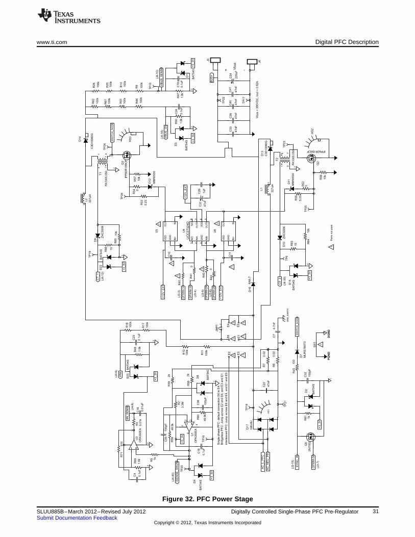
The non-isolated UART interface shown in Figure 33 is used to control the PFC module from the host PCover the serial port. It is also used to monitor some of the parameters, debug and test firmware functions.
Figure 33. Non-Isolated PFC Module to Host PC Interface
32 Digitally Controlled Single-Phase PFC Pre-Regulator SLUU885B–March 2012–Revised July 2012Submit Documentation Feedback
Copyright © 2012, Texas Instruments Incorporated
www.ti.com Digital PFC Description
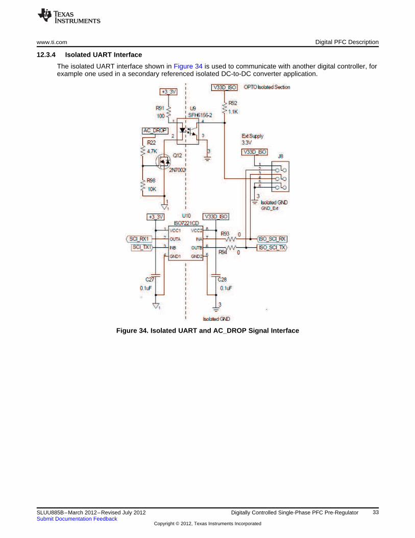
12.3.4 Isolated UART Interface
The isolated UART interface shown in Figure 34 is used to communicate with another digital controller, forexample one used in a secondary referenced isolated DC-to-DC converter application.
Figure 34. Isolated UART and AC_DROP Signal Interface
33SLUU885B–March 2012–Revised July 2012 Digitally Controlled Single-Phase PFC Pre-RegulatorSubmit Documentation Feedback
Copyright © 2012, Texas Instruments Incorporated
Digital PFC Description www.ti.com
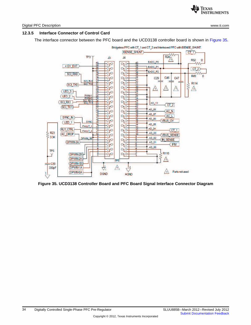
12.3.5 Interface Connector of Control Card
The interface connector between the PFC board and the UCD3138 controller board is shown in Figure 35.
Figure 35. UCD3138 Controller Board and PFC Board Signal Interface Connector Diagram
34 Digitally Controlled Single-Phase PFC Pre-Regulator SLUU885B–March 2012–Revised July 2012Submit Documentation Feedback
Copyright © 2012, Texas Instruments Incorporated
www.ti.com Digital PFC Description
12.3.6 UCD3138 Resource Allocation for PFC Control
Table 5. J3 and J4 Pin Assignment
UCD3138 CONTROLHEADER PIN NUMBER DESCRIPTIONCARD PIN NAME
J3-1 DPWM_0A RC filter for debug monitoring
J3-2 DPWM_0B Not used
J3-3 DPWM_1A Not used(available as an option for PFC PWM1)
J3-4 DPWM_1B PFC PWM1
J3-5 DPWM_2A Not used(available as an option for PFC PWM2)
J3-6 DPWM_2B PFC PWM2
J3-7 DPWM_3A PFC ZVS control
J3-8 DPWM_3B AC drop indicator signal
J3-9 DGND Digital ground GND1
J3-10 DGND Digital ground GND1
J3-11 FAULT-0 Inrush relay control
J3-12 Not used Not used
J3-13 FAULT-1 LED 1
J3-14 Not used Not used
J3-15 SYNC Sync input signal for PFC stage
J3-16 Not used Not used
J3-17 FAULT-2 Not used
J3-18 Not used Not used
J3-19 Not used Not used
J3-20 Not used Not used
J3-21 Not used Not used
J3-22 FAULT-3 Not used
J3-23 SCI_TX1 SCI_TX1
J3-24 SCI_RX1 SCI_RX1
J3-25 PWM0 LED 2
J3-26 PWM1 LED 3
J3-27 Not used Not used
J3-28 Not used Not used
J3-29 TCAP Not used
J3-30 Not used Not used
J3-31 SCI TX0 SCI TX0
J3-32 SCI TX0 SCI RX0
J3-33 INT-EXT Not used
J3-34 EXT-TRIG Not used
J3-35 DGND Not used
J3-36 RESET* Not used
J3-37 DGND Digital ground GND1
J3-38 DGND Digital ground GND1
J3-39 +12V_EXT External +12V DC supply
J3-40 3.3VD Not used
J4-01 AGND Analog ground GND2
J4-02 Not used Not used
J4-03 AGND Analog ground GND2
J4-04 AD_00 PMBus address
J4-05 AGND Analog ground GND2
35SLUU885B–March 2012–Revised July 2012 Digitally Controlled Single-Phase PFC Pre-RegulatorSubmit Documentation Feedback
Copyright © 2012, Texas Instruments Incorporated
Digital PFC Description www.ti.com
Table 5. J3 and J4 Pin Assignment (continued)
UCD3138 CONTROLHEADER PIN NUMBER DESCRIPTIONCARD PIN NAME
J4-06 AD_01 IPM
J4-07 AGND Analog ground GND2
J4-08 AD_02 PFC input current sense
J4-09 AGND Analog ground GND2
J4-10 AD_03 PFC BUS voltage sense
J4-11 AGND Analog ground GND2
J4-12 AD_04 PFC MOSFET Q3 current sense
J4-13 AGND Analog ground GND2
J4-14 AD_05 Not used
J4-15 AGND Analog ground GND2
J4-16 AD_06 PFC BUS voltage sense(for OVP)
J4-17 AGND Analog ground GND2
J4-18 AD_07 PFC Vin line voltage sense
J4-19 AGND Analog ground GND2
J4-20 AD_08 PFC Vin neutral voltage sense
J4-21 AGND Analog ground GND2
J4-22 AD_09 Not used
J4-23 AGND Analog ground GND2
J4-24 AD_10 Not used
J4-25 AGND Analog ground GND2
J4-26 AD_11 Not used
J4-27 AGND Analog ground GND2
J4-28 AD_12 Not used
J4-29 AGND Analog ground GND2
J4-30 AD_13 PFC MOSFET Q4 current sense
J4-31 AGND Analog ground GND2
J4-32 Not used Not used
J4-33 Not used Not used
J4-34 Not used Not used
J4-35 EAN2 Analog ground GND2
J4-36 EAP2 PFC MOSFET Q4 current sense
J4-37 EAN1 Analog ground GND2
J4-38 EAP1 PFC MOSFET Q3 current sense
J4-39 EAN0 Analog ground GND2
J4-40 EAP0 PFC Input current sense
36 Digitally Controlled Single-Phase PFC Pre-Regulator SLUU885B–March 2012–Revised July 2012Submit Documentation Feedback
Copyright © 2012, Texas Instruments Incorporated
Background Loop· System initialization· Voltage feed forward
· System monitoring· Dynamic coefficient adjustment
· PMBus communication
· UART transmit data
Standard interrupt· ADC measurement· State machine
· Vrms calculation· Voltage loop calculation
· Current reference calculation
· AC drop detection· UART receive data
· Frequency dithering· ZVS control
Fast interrupt· OVP
www.ti.com Digital PFC Description
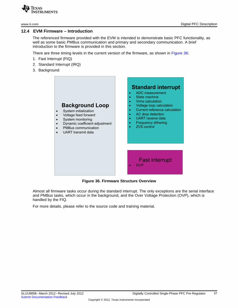
12.4 EVM Firmware – Introduction
The referenced firmware provided with the EVM is intended to demonstrate basic PFC functionality, aswell as some basic PMBus communication and primary and secondary communication. A briefintroduction to the firmware is provided in this section.
There are three timing levels in the current version of the firmware, as shown in Figure 36:
1. Fast Interrupt (FIQ)
2. Standard Interrupt (IRQ)
3. Background
Figure 36. Firmware Structure Overview
Almost all firmware tasks occur during the standard interrupt. The only exceptions are the serial interfaceand PMBus tasks, which occur in the background, and the Over Voltage Protection (OVP), which ishandled by the FIQ.
For more details, please refer to the source code and training material.
37SLUU885B–March 2012–Revised July 2012 Digitally Controlled Single-Phase PFC Pre-RegulatorSubmit Documentation Feedback
Copyright © 2012, Texas Instruments Incorporated
Digital PFC Description www.ti.com
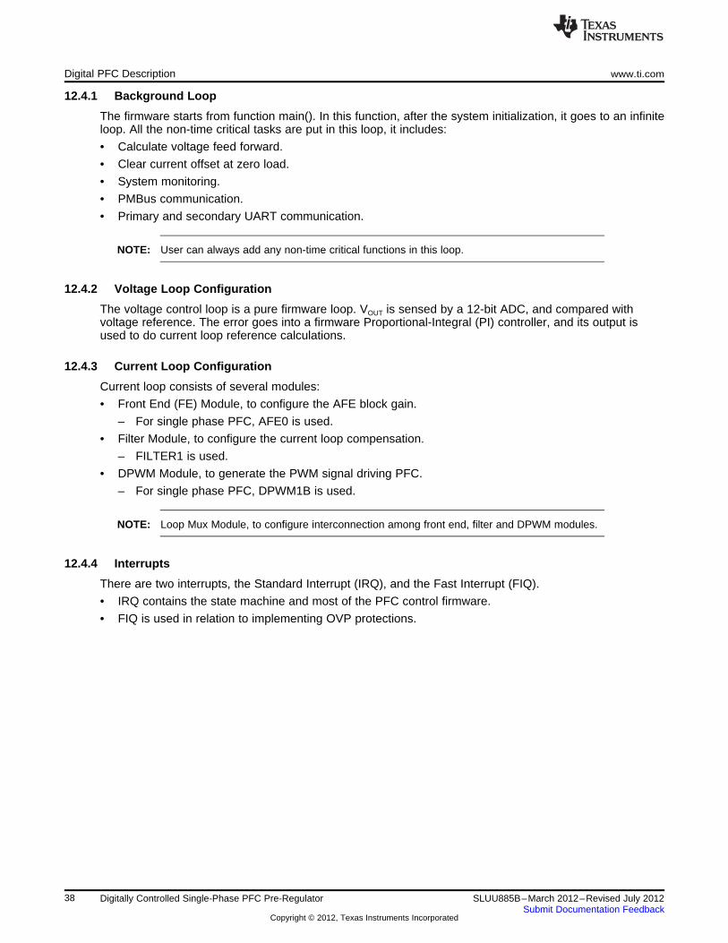
12.4.1 Background Loop
The firmware starts from function main(). In this function, after the system initialization, it goes to an infiniteloop. All the non-time critical tasks are put in this loop, it includes:
• Calculate voltage feed forward.
• Clear current offset at zero load.
• System monitoring.
• PMBus communication.
• Primary and secondary UART communication.
NOTE: User can always add any non-time critical functions in this loop.
12.4.2 Voltage Loop Configuration
The voltage control loop is a pure firmware loop. VOUT is sensed by a 12-bit ADC, and compared withvoltage reference. The error goes into a firmware Proportional-Integral (PI) controller, and its output isused to do current loop reference calculations.
12.4.3 Current Loop Configuration
Current loop consists of several modules:
• Front End (FE) Module, to configure the AFE block gain.
– For single phase PFC, AFE0 is used.
• Filter Module, to configure the current loop compensation.
– FILTER1 is used.
• DPWM Module, to generate the PWM signal driving PFC.
– For single phase PFC, DPWM1B is used.
NOTE: Loop Mux Module, to configure interconnection among front end, filter and DPWM modules.
12.4.4 Interrupts
There are two interrupts, the Standard Interrupt (IRQ), and the Fast Interrupt (FIQ).
• IRQ contains the state machine and most of the PFC control firmware.
• FIQ is used in relation to implementing OVP protections.
38 Digitally Controlled Single-Phase PFC Pre-Regulator SLUU885B–March 2012–Revised July 2012Submit Documentation Feedback
Copyright © 2012, Texas Instruments Incorporated
Idle
Relay
close
Ramp up
PFCon
PFChiccup
PFC shutdownand
latch
Vin > 90V
after100ms
Vout = 390VVout >420V
Vout < 380V
Vout >420 V
Vout >435V
Vin<
85 V
www.ti.com Digital PFC Description
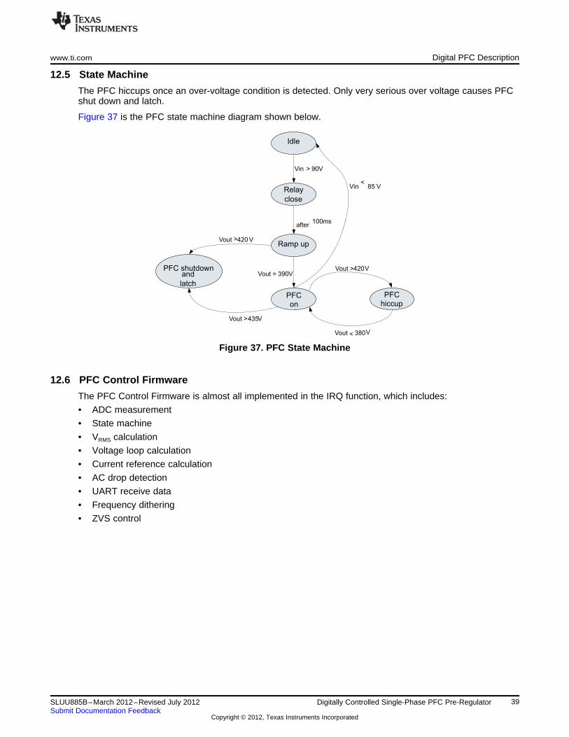
12.5 State Machine
The PFC hiccups once an over-voltage condition is detected. Only very serious over voltage causes PFCshut down and latch.
Figure 37 is the PFC state machine diagram shown below.
Figure 37. PFC State Machine
12.6 PFC Control Firmware
The PFC Control Firmware is almost all implemented in the IRQ function, which includes:
• ADC measurement
• State machine
• VRMS calculation
• Voltage loop calculation
• Current reference calculation
• AC drop detection
• UART receive data
• Frequency dithering
• ZVS control
39SLUU885B–March 2012–Revised July 2012 Digitally Controlled Single-Phase PFC Pre-RegulatorSubmit Documentation Feedback
Copyright © 2012, Texas Instruments Incorporated
Digital PFC Description www.ti.com
12.7 System Protection
12.7.1 Cycle-by-Cycle Current Protection (CBC)
The cycle-by-cycle current protection is achieved through AD04 (Comparator D) and AD13 (ComparatorE). Once the current signal has exceeded the threshold, the PWM is chopped to limit the current.
12.7.2 Over-Voltage Protection (OVP)
There are two levels of OVP that exist. Under fault condition if the output voltage reaches 420 V, a non-latched OV protection is activated. Under this condition the output oscillates between 420 V and 380 V.
In the event of a more severe overvoltage condition, if the output reaches to 435 V, the latched over-voltage protection is activated and the unit is completely shut off.
The FIQ is currently used only for latched over-voltage protection. It is triggered by the comparator onAD06 (Comparator F). Comparator F’s threshold is set above the limit for the DC bus voltage, and thelogic on DPWM1 and DPWM2 is set up to turn off DPWM1B and DPWM2B when the threshold isexceeded. In the current configuration, the only way to restart the PFC after a latched OVP fault is to resetthe processor.
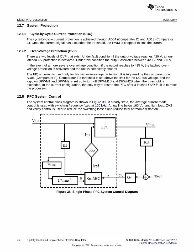
12.8 PFC System Control
The system control block diagram is shown in Figure 38. In steady state, the average current-modecontrol is used with switching frequency fixed at 100 kHz. At low line below 160 VAC and light load, ZVSand valley control is used to reduce the switching losses and reduce total harmonic distortion.
Figure 38. Single-Phase PFC System Control Diagram
40 Digitally Controlled Single-Phase PFC Pre-Regulator SLUU885B–March 2012–Revised July 2012Submit Documentation Feedback
Copyright © 2012, Texas Instruments Incorporated
LB
RLOAD
RL
Vin
Vout
RD S_ON VsenseRD1
RD 2
CP1
Gatedriver
Iref
Analog- to - PWMGain = 1
PIDCompensator
K P, KI, K D,
and Ts
RS
R3R4
CP2
m f MIN(pk)K 0.5 K V= ´ ´
( ) ( )REF m m v f IN 2RMS
1I K A C B K U K V
V
æ öç ÷= ´ ´ ´ = ´ ´ ´ ´ç ÷è ø
www.ti.com Digital PFC Description
12.8.1 Average Current Mode Control
The current loop is shown in the dashed line of Figure 38. The current reference signal IREF is calculatedas:
where• Km – multiplier gain• A – voltage loop output• B – 1/(VIN(rms))2• C – VIN (1)
For sine wave input, the multiplier gain Km is expressed as,
(2)
In Figure 27, Ks and Kf are scaling factors. For further detail, please refer to reference , and .
12.8.2 ZVS and Valley Control
Please refer to the reference and .
12.9 Current Feedback Control Compensation Using PID Control
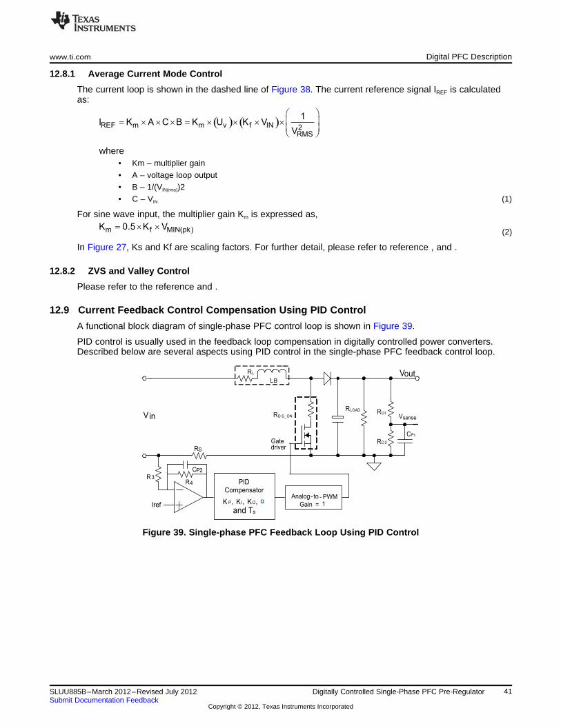
A functional block diagram of single-phase PFC control loop is shown in Figure 39.
PID control is usually used in the feedback loop compensation in digitally controlled power converters.Described below are several aspects using PID control in the single-phase PFC feedback control loop.
Figure 39. Single-phase PFC Feedback Loop Using PID Control
41SLUU885B–March 2012–Revised July 2012 Digitally Controlled Single-Phase PFC Pre-RegulatorSubmit Documentation Feedback
Copyright © 2012, Texas Instruments Incorporated
Q 0.5£
z1 z2
z1 z2
Qw ´ w
=
w + w
r z1 z2w = w ´ w
2rz1, z2 1 1 4 Q
2 Q
w æ öw = ± - ´ç ÷´ è ø
2
2rr
cz 0
p1
s s1
QG (s) K
ss 1
æ öç ÷+ +ç ÷´ wwè ø=
æ ö+ç ÷
ç ÷wè ø
z1 z2cz 0
p1
s s1 1
G (s) Ks
s 1
æ öæ ö+ +ç ÷ç ÷
w wè øè ø=æ ö
+ç ÷ç ÷wè ø
1 1
c P I D1 1
1 z 1 zG (z) K K K
1 z 1 z
- -
- -
+ -= + +
- - a´
Digital PFC Description www.ti.com
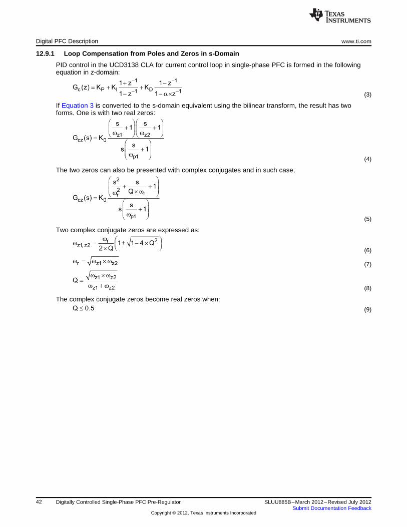
12.9.1 Loop Compensation from Poles and Zeros in s-Domain
PID control in the UCD3138 CLA for current control loop in single-phase PFC is formed in the followingequation in z-domain:
(3)
If Equation 3 is converted to the s-domain equivalent using the bilinear transform, the result has twoforms. One is with two real zeros:
(4)
The two zeros can also be presented with complex conjugates and in such case,
(5)
Two complex conjugate zeros are expressed as:
(6)
(7)
(8)
The complex conjugate zeros become real zeros when:
(9)
42 Digitally Controlled Single-Phase PFC Pre-Regulator SLUU885B–March 2012–Revised July 2012Submit Documentation Feedback
Copyright © 2012, Texas Instruments Incorporated
s p1
s p1
2 T
2 T
- ´ w
a =
+ ´ w
( ) ( )( )
0 p1 z1 p1 z2
D
p1 z1 z2 s p1
2 KK
T 2
´ ´ w - w ´ w - w=
w ´ w ´ w ´ w +
0 sI
K TK
2
´
=
( )0 p1 z1 p1 z2 z1 z2
Pp1 z1 z2
KK
´ w ´ w + w ´ w - w ´ w=
w ´ w ´ w
Bs
s B
L1T 0.05
f R= £ ´
M PIDcs
M PID cs
G (s) G (s)G (s)
1 G (s) G (s) H (s)
´
=
+ ´ ´
4cs s
3
pcs
R 1H (s) R
sR1
= ´
+
w
pcs4 p2
1
R Cw =
´
www.ti.com Digital PFC Description
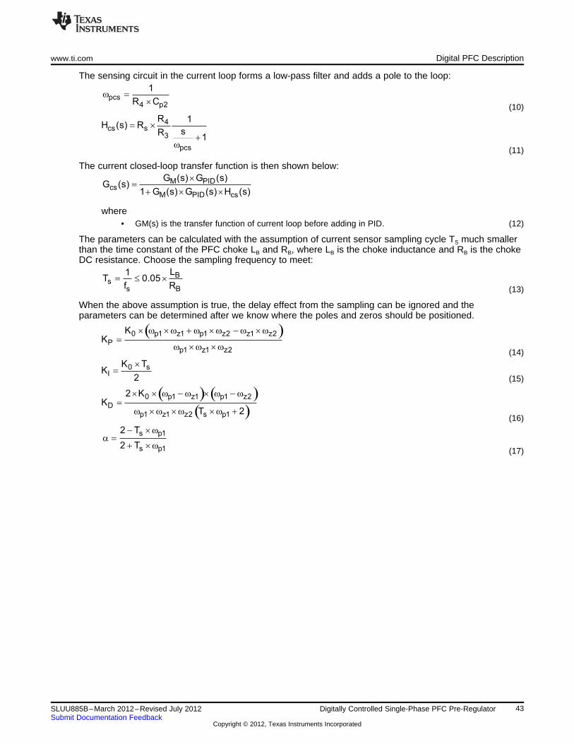
The sensing circuit in the current loop forms a low-pass filter and adds a pole to the loop:
(10)
(11)
The current closed-loop transfer function is then shown below:
where• GM(s) is the transfer function of current loop before adding in PID. (12)
The parameters can be calculated with the assumption of current sensor sampling cycle TS much smallerthan the time constant of the PFC choke LB and RB, where LB is the choke inductance and RB is the chokeDC resistance. Choose the sampling frequency to meet:
(13)
When the above assumption is true, the delay effect from the sampling can be ignored and theparameters can be determined after we know where the poles and zeros should be positioned.
(14)
(15)
(16)
(17)
43SLUU885B–March 2012–Revised July 2012 Digitally Controlled Single-Phase PFC Pre-RegulatorSubmit Documentation Feedback
Copyright © 2012, Texas Instruments Incorporated
Frequency
KI
KP
KD
Zero 1 Zero 2
Pole 2
Increasing fs causes the whole Bode plots to shift to right
Pole 1
Gain
Digital PFC Description www.ti.com
12.9.2 Feedback Loop Compenstaion Tuning with PID Coefficients
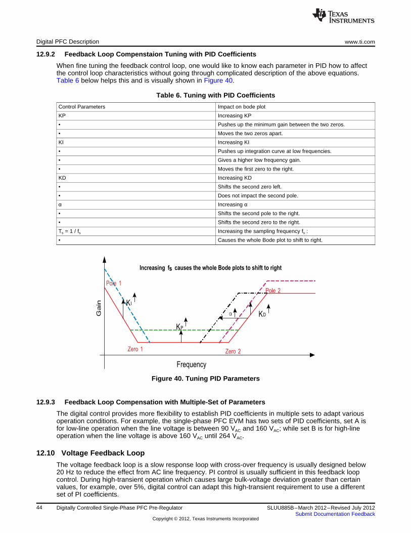
When fine tuning the feedback control loop, one would like to know each parameter in PID how to affectthe control loop characteristics without going through complicated description of the above equations.Table 6 below helps this and is visually shown in Figure 40.
Table 6. Tuning with PID Coefficients
Control Parameters Impact on bode plot
KP Increasing KP
• Pushes up the minimum gain between the two zeros.
• Moves the two zeros apart.
KI Increasing KI
• Pushes up integration curve at low frequencies.
• Gives a higher low frequency gain.
• Moves the first zero to the right.
KD Increasing KD
• Shifts the second zero left.
• Does not impact the second pole.
α Increasing α• Shifts the second pole to the right.
• Shifts the second zero to the right.
Ts = 1 / fs Increasing the sampling frequency fs :
• Causes the whole Bode plot to shift to right.
Figure 40. Tuning PID Parameters
12.9.3 Feedback Loop Compensation with Multiple-Set of Parameters
The digital control provides more flexibility to establish PID coefficients in multiple sets to adapt variousoperation conditions. For example, the single-phase PFC EVM has two sets of PID coefficients, set A isfor low-line operation when the line voltage is between 90 VAC and 160 VAC; while set B is for high-lineoperation when the line voltage is above 160 VAC until 264 VAC.
12.10 Voltage Feedback Loop
The voltage feedback loop is a slow response loop with cross-over frequency is usually designed below20 Hz to reduce the effect from AC line frequency. PI control is usually sufficient in this feedback loopcontrol. During high-transient operation which causes large bulk-voltage deviation greater than certainvalues, for example, over 5%, digital control can adapt this high-transient requirement to use a differentset of PI coefficients.
44 Digitally Controlled Single-Phase PFC Pre-Regulator SLUU885B–March 2012–Revised July 2012Submit Documentation Feedback
Copyright © 2012, Texas Instruments Incorporated
www.ti.com Evaluating the Single-Phase PFC with GUI
13 Evaluating the Single-Phase PFC with GUI
Further evaluation of UCD3138PFCEVM-026 can be made with the designer GUI while no need to directlyaccess the firmware codes. The designer GUI, called Fusion Digital Power Designer is described inSection 13.1. The description is given on how to use the GUI to make further evaluation ofUCD3138PFCEVM-026.
13.1 Graphical User Interface (GUI)
Collectively, the GUI is called Texas Instruments Fusion Digital Power Designer. The GUI serves theinterface for several families of TI digital control devices including the family of UCD31xx, that is theUCD3138 as its one member. The GUI can be divided into two main categories, Designer GUI and DeviceGUI. In the family of UCD31xx, each EVM is related to a particular Designer GUI to allow users to re-tune/re-configure a particular EVM in that regarding with existing hardware and firmware. Device GUI isrelated to a particular device to access its internal registers and memories.
UCD3138PFCEVM-026 is used with its control card UCD3138CC64EVM-030 where UCD3138 device isplaced. The firmware for single-phase PFC control is loaded into UCD3138CC64EVM-030 board throughdevice GUI. How to install the GUI is described in the user’s guide Using the UCD3138CC64EVM-030 (TILiturature Number, SLUU886). The designer GUI is installed at the same time when installing the deviceGUI.
13.2 Open the Designer GUI
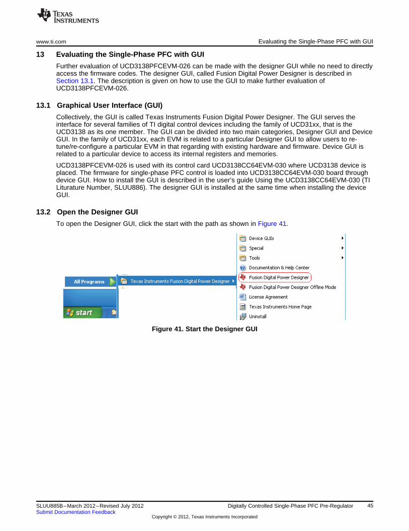
To open the Designer GUI, click the start with the path as shown in Figure 41.
Figure 41. Start the Designer GUI
45SLUU885B–March 2012–Revised July 2012 Digitally Controlled Single-Phase PFC Pre-RegulatorSubmit Documentation Feedback
Copyright © 2012, Texas Instruments Incorporated
Evaluating the Single-Phase PFC with GUI www.ti.com
13.3 Overview of the Designer GUI
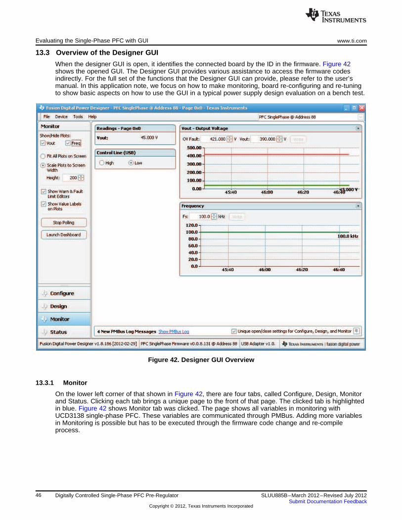
When the designer GUI is open, it identifies the connected board by the ID in the firmware. Figure 42shows the opened GUI. The Designer GUI provides various assistance to access the firmware codesindirectly. For the full set of the functions that the Designer GUI can provide, please refer to the user’smanual. In this application note, we focus on how to make monitoring, board re-configuring and re-tuningto show basic aspects on how to use the GUI in a typical power supply design evaluation on a bench test.
Figure 42. Designer GUI Overview
13.3.1 Monitor
On the lower left corner of that shown in Figure 42, there are four tabs, called Configure, Design, Monitorand Status. Clicking each tab brings a unique page to the front of that page. The clicked tab is highlightedin blue. Figure 42 shows Monitor tab was clicked. The page shows all variables in monitoring withUCD3138 single-phase PFC. These variables are communicated through PMBus. Adding more variablesin Monitoring is possible but has to be executed through the firmware code change and re-compileprocess.
46 Digitally Controlled Single-Phase PFC Pre-Regulator SLUU885B–March 2012–Revised July 2012Submit Documentation Feedback
Copyright © 2012, Texas Instruments Incorporated
www.ti.com Evaluating the Single-Phase PFC with GUI
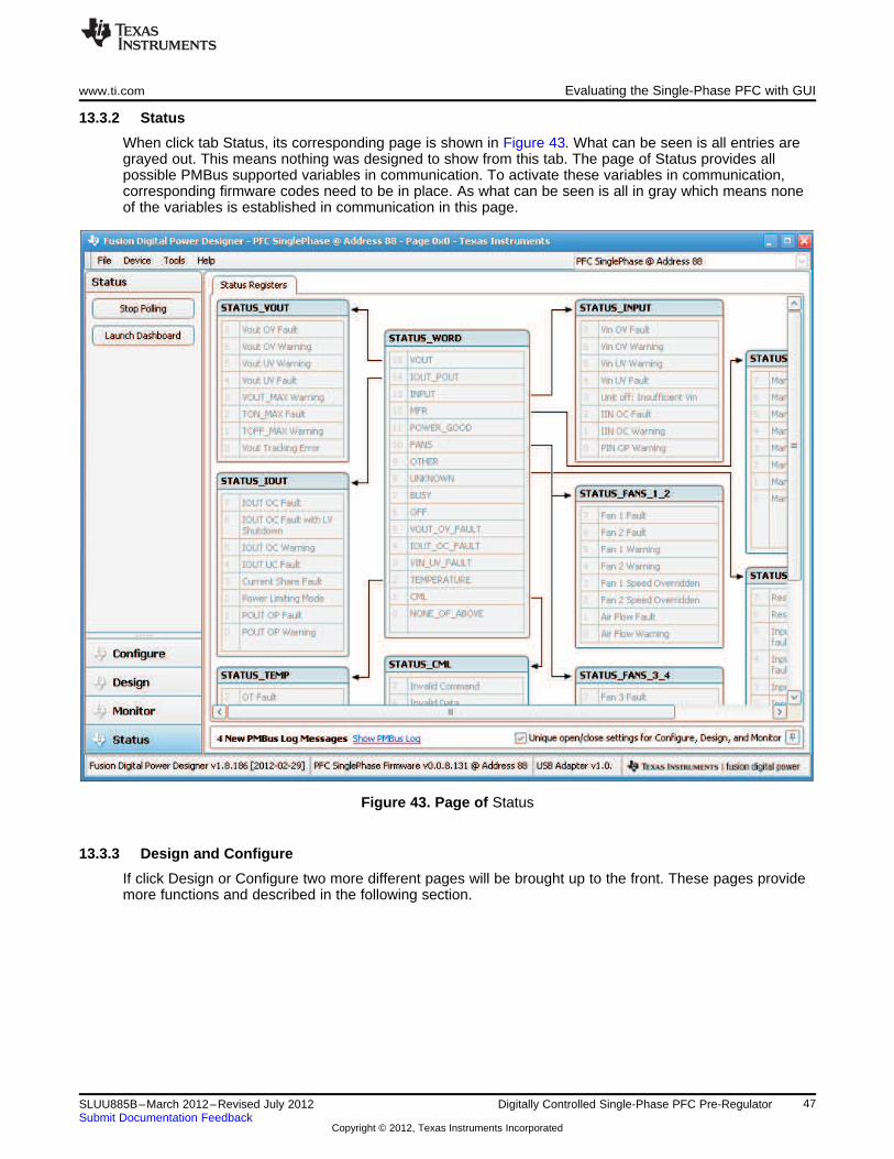
13.3.2 Status
When click tab Status, its corresponding page is shown in Figure 43. What can be seen is all entries aregrayed out. This means nothing was designed to show from this tab. The page of Status provides allpossible PMBus supported variables in communication. To activate these variables in communication,corresponding firmware codes need to be in place. As what can be seen is all in gray which means noneof the variables is established in communication in this page.
Figure 43. Page of Status
13.3.3 Design and Configure
If click Design or Configure two more different pages will be brought up to the front. These pages providemore functions and described in the following section.
47SLUU885B–March 2012–Revised July 2012 Digitally Controlled Single-Phase PFC Pre-RegulatorSubmit Documentation Feedback
Copyright © 2012, Texas Instruments Incorporated
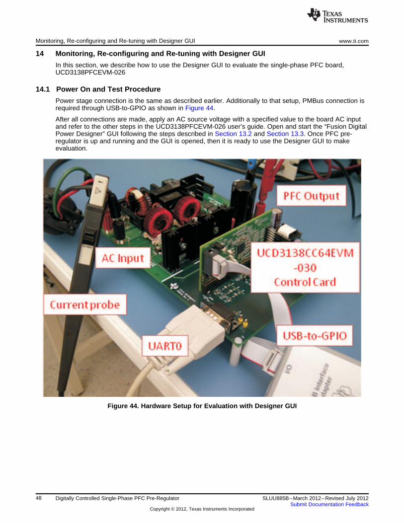
Monitoring, Re-configuring and Re-tuning with Designer GUI www.ti.com
14 Monitoring, Re-configuring and Re-tuning with Designer GUI
In this section, we describe how to use the Designer GUI to evaluate the single-phase PFC board,UCD3138PFCEVM-026
14.1 Power On and Test Procedure
Power stage connection is the same as described earlier. Additionally to that setup, PMBus connection isrequired through USB-to-GPIO as shown in Figure 44.
After all connections are made, apply an AC source voltage with a specified value to the board AC inputand refer to the other steps in the UCD3138PFCEVM-026 user’s guide. Open and start the “Fusion DigitalPower Designer” GUI following the steps described in Section 13.2 and Section 13.3. Once PFC pre-regulator is up and running and the GUI is opened, then it is ready to use the Designer GUI to makeevaluation.
Figure 44. Hardware Setup for Evaluation with Designer GUI
48 Digitally Controlled Single-Phase PFC Pre-Regulator SLUU885B–March 2012–Revised July 2012Submit Documentation Feedback
Copyright © 2012, Texas Instruments Incorporated

www.ti.com Monitoring, Re-configuring and Re-tuning with Designer GUI
14.2 Monitoring with GUI
The page shows three variables in monitoring:
• VOUT – PFC output bulk voltage.
• OV Fault – PFC output bulk voltage over voltage fault threshold.
• Freq – switching frequency in normal operation.
Among three monitoring variables, we can see VOUT and OV Fault can be accessed by write to changethem to a different value into the firmware. However, when attempting to do so, make sure to understandthe design of all aspects to avoid any possible damage. As a warning to help avoid damage, if one wantsto modify “Vout” or “OV Fault” to a different value, the recommendation is 375 V to 395 V for VOUT, and notexceeding 430 V for OV Fault. Also, logically, VOUT has to be smaller than OV Fault.
One may modify them to other values but before doing that, fully understanding the design is needed tofind out any other parameters needed to change accordingly such that not over stress the components inuse or inducing any stability concerns.
49SLUU885B–March 2012–Revised July 2012 Digitally Controlled Single-Phase PFC Pre-RegulatorSubmit Documentation Feedback
Copyright © 2012, Texas Instruments Incorporated
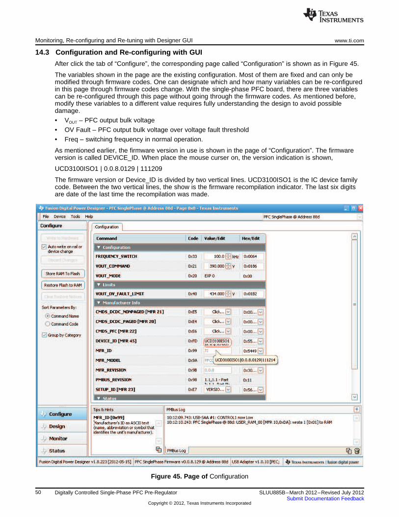
Monitoring, Re-configuring and Re-tuning with Designer GUI www.ti.com
14.3 Configuration and Re-configuring with GUI
After click the tab of “Configure”, the corresponding page called “Configuration” is shown as in Figure 45.
The variables shown in the page are the existing configuration. Most of them are fixed and can only bemodified through firmware codes. One can designate which and how many variables can be re-configuredin this page through firmware codes change. With the single-phase PFC board, there are three variablescan be re-configured through this page without going through the firmware codes. As mentioned before,modify these variables to a different value requires fully understanding the design to avoid possibledamage.
• VOUT – PFC output bulk voltage
• OV Fault – PFC output bulk voltage over voltage fault threshold
• Freq – switching frequency in normal operation.
As mentioned earlier, the firmware version in use is shown in the page of “Configuration”. The firmwareversion is called DEVICE_ID. When place the mouse curser on, the version indication is shown,
UCD3100ISO1 | 0.0.8.0129 | 111209
The firmware version or Device_ID is divided by two vertical lines. UCD3100ISO1 is the IC device familycode. Between the two vertical lines, the show is the firmware recompilation indicator. The last six digitsare date of the last time the recompilation was made.
Figure 45. Page of Configuration
50 Digitally Controlled Single-Phase PFC Pre-Regulator SLUU885B–March 2012–Revised July 2012Submit Documentation Feedback
Copyright © 2012, Texas Instruments Incorporated
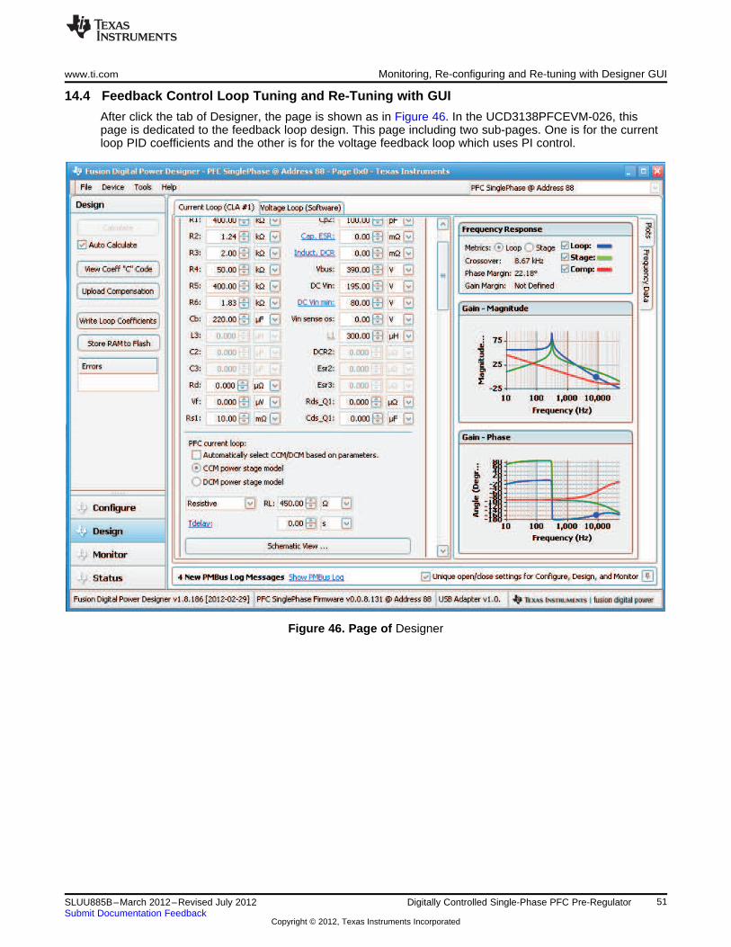
www.ti.com Monitoring, Re-configuring and Re-tuning with Designer GUI
14.4 Feedback Control Loop Tuning and Re-Tuning with GUI
After click the tab of Designer, the page is shown as in Figure 46. In the UCD3138PFCEVM-026, thispage is dedicated to the feedback loop design. This page including two sub-pages. One is for the currentloop PID coefficients and the other is for the voltage feedback loop which uses PI control.
Figure 46. Page of Designer
51SLUU885B–March 2012–Revised July 2012 Digitally Controlled Single-Phase PFC Pre-RegulatorSubmit Documentation Feedback
Copyright © 2012, Texas Instruments Incorporated
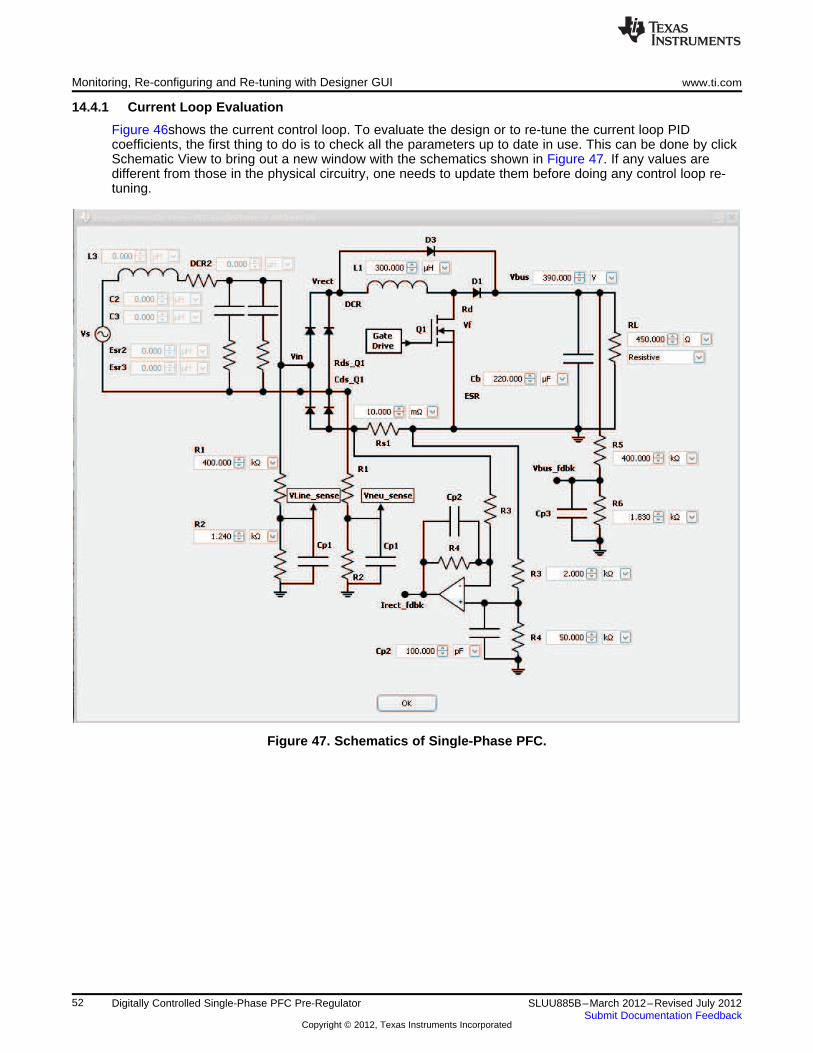
Monitoring, Re-configuring and Re-tuning with Designer GUI www.ti.com
14.4.1 Current Loop Evaluation
Figure 46shows the current control loop. To evaluate the design or to re-tune the current loop PIDcoefficients, the first thing to do is to check all the parameters up to date in use. This can be done by clickSchematic View to bring out a new window with the schematics shown in Figure 47. If any values aredifferent from those in the physical circuitry, one needs to update them before doing any control loop re-tuning.
Figure 47. Schematics of Single-Phase PFC.
52 Digitally Controlled Single-Phase PFC Pre-Regulator SLUU885B–March 2012–Revised July 2012Submit Documentation Feedback
Copyright © 2012, Texas Instruments Incorporated
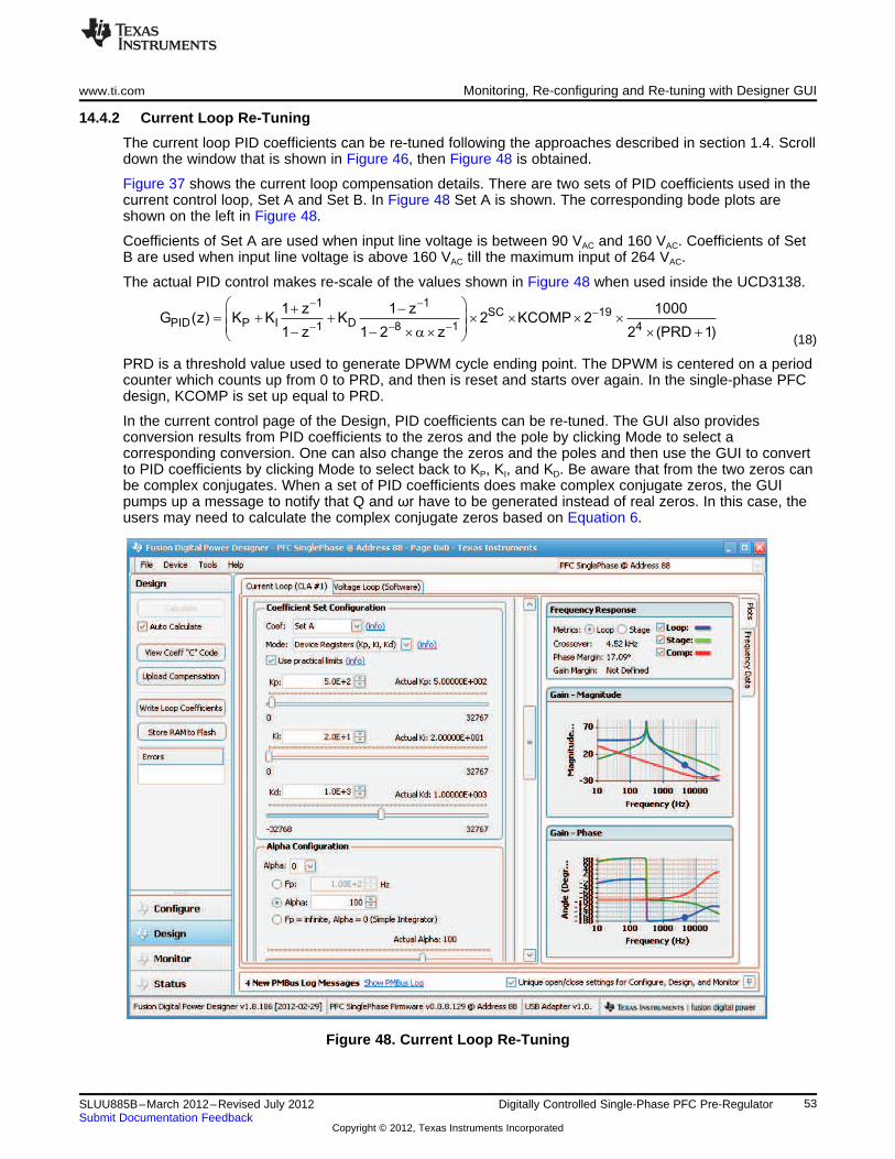
1 1SC 19
PID P I D1 8 1 4
1 z 1 z 1000G (z) K K K 2 KCOMP 2
1 z 1 2 z 2 (PRD 1)
- --
- - -
æ ö+ -= + + ´ ´ ´ ´ç ÷
ç ÷- - ´ a ´ ´ +è ø
www.ti.com Monitoring, Re-configuring and Re-tuning with Designer GUI
14.4.2 Current Loop Re-Tuning
The current loop PID coefficients can be re-tuned following the approaches described in section 1.4. Scrolldown the window that is shown in Figure 46, then Figure 48 is obtained.
Figure 37 shows the current loop compensation details. There are two sets of PID coefficients used in thecurrent control loop, Set A and Set B. In Figure 48 Set A is shown. The corresponding bode plots areshown on the left in Figure 48.
Coefficients of Set A are used when input line voltage is between 90 VAC and 160 VAC. Coefficients of SetB are used when input line voltage is above 160 VAC till the maximum input of 264 VAC.
The actual PID control makes re-scale of the values shown in Figure 48 when used inside the UCD3138.
(18)
PRD is a threshold value used to generate DPWM cycle ending point. The DPWM is centered on a periodcounter which counts up from 0 to PRD, and then is reset and starts over again. In the single-phase PFCdesign, KCOMP is set up equal to PRD.
In the current control page of the Design, PID coefficients can be re-tuned. The GUI also providesconversion results from PID coefficients to the zeros and the pole by clicking Mode to select acorresponding conversion. One can also change the zeros and the poles and then use the GUI to convertto PID coefficients by clicking Mode to select back to KP, KI, and KD. Be aware that from the two zeros canbe complex conjugates. When a set of PID coefficients does make complex conjugate zeros, the GUIpumps up a message to notify that Q and ωr have to be generated instead of real zeros. In this case, theusers may need to calculate the complex conjugate zeros based on Equation 6.
Figure 48. Current Loop Re-Tuning
53SLUU885B–March 2012–Revised July 2012 Digitally Controlled Single-Phase PFC Pre-RegulatorSubmit Documentation Feedback
Copyright © 2012, Texas Instruments Incorporated
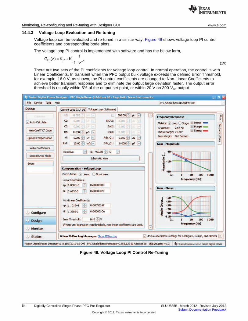
PI P I 1
1G (z) K K
1 z-
= +
-
Monitoring, Re-configuring and Re-tuning with Designer GUI www.ti.com
14.4.3 Voltage Loop Evaluation and Re-tuning
Voltage loop can be evaluated and re-tuned in a similar way. Figure 49 shows voltage loop PI controlcoefficients and corresponding bode plots.
The voltage loop PI control is implemented with software and has the below form,
(19)
There are two sets of the PI coefficients for voltage loop control. In normal operation, the control is withLinear Coefficients. In transient when the PFC output bulk voltage exceeds the defined Error Threshold,for example, 16.0 V, as shown, the PI control coefficients are changed to Non-Linear Coefficients toachieve better transient response and to eliminate the output large deviation faster. The output errorthreshold is usually within 5% of the output set point, or within 20 V on 390-VDC output.
Figure 49. Voltage Loop PI Control Re-Tuning
54 Digitally Controlled Single-Phase PFC Pre-Regulator SLUU885B–March 2012–Revised July 2012Submit Documentation Feedback
Copyright © 2012, Texas Instruments Incorporated
www.ti.com Digital PFC Firmware Development
15 Digital PFC Firmware Development
Please contact TI for additional information regarding UCD3138 digital PFC firmware development.
16 References1. UCD3138 Datasheet, SLUSAP2, 2012
2. UCD3138CC64EVM-030 Evaluation Module and User’s Guide, SLUU886, 2012
3. SEM600, 1988, High Power Factor Pre-regulator for Off-line Power Supplies
4. SEM700, 1990, Optimizing the Design of a High Power Factor Switching Pre-regulator
5. TI Application Note SLUA644, “PFC THD Reduction and Efficiency Improvement by ZVS or ValleySwitching”, April 2012.
6. Zhong Ye and Bosheng Sun, “PFC Efficiency Improvement and THD Reduction at Light Loads withZVS and Valley Switching”, APEC 2012, pp 802-806
7. UCD3138 Digital Power Peripherals Programmer’s Manual (please contact TI)
8. UCD3138 Monitoring and Communications Programmer’s Manual (please contact TI)
9. UCD3138 ARM and Digital System Programmer’s Manual (please contact TI)
10. UCD3138 Isolated Power Fusion GUI User Guide (please contact TI)
55SLUU885B–March 2012–Revised July 2012 Digitally Controlled Single-Phase PFC Pre-RegulatorSubmit Documentation Feedback
Copyright © 2012, Texas Instruments Incorporated

EVALUATION BOARD/KIT/MODULE (EVM) ADDITIONAL TERMS
Texas Instruments (TI) provides the enclosed Evaluation Board/Kit/Module (EVM) under the following conditions:
The user assumes all responsibility and liability for proper and safe handling of the goods. Further, the user indemnifies TI from all claimsarising from the handling or use of the goods.
Should this evaluation board/kit not meet the specifications indicated in the User’s Guide, the board/kit may be returned within 30 days fromthe date of delivery for a full refund. THE FOREGOING LIMITED WARRANTY IS THE EXCLUSIVE WARRANTY MADE BY SELLER TOBUYER AND IS IN LIEU OF ALL OTHER WARRANTIES, EXPRESSED, IMPLIED, OR STATUTORY, INCLUDING ANY WARRANTY OFMERCHANTABILITY OR FITNESS FOR ANY PARTICULAR PURPOSE. EXCEPT TO THE EXTENT OF THE INDEMNITY SET FORTHABOVE, NEITHER PARTY SHALL BE LIABLE TO THE OTHER FOR ANY INDIRECT, SPECIAL, INCIDENTAL, OR CONSEQUENTIALDAMAGES.
Please read the User's Guide and, specifically, the Warnings and Restrictions notice in the User's Guide prior to handling the product. Thisnotice contains important safety information about temperatures and voltages. For additional information on TI's environmental and/or safetyprograms, please visit www.ti.com/esh or contact TI.
No license is granted under any patent right or other intellectual property right of TI covering or relating to any machine, process, orcombination in which such TI products or services might be or are used. TI currently deals with a variety of customers for products, andtherefore our arrangement with the user is not exclusive. TI assumes no liability for applications assistance, customer product design,software performance, or infringement of patents or services described herein.
REGULATORY COMPLIANCE INFORMATION
As noted in the EVM User’s Guide and/or EVM itself, this EVM and/or accompanying hardware may or may not be subject to the FederalCommunications Commission (FCC) and Industry Canada (IC) rules.
For EVMs not subject to the above rules, this evaluation board/kit/module is intended for use for ENGINEERING DEVELOPMENT,DEMONSTRATION OR EVALUATION PURPOSES ONLY and is not considered by TI to be a finished end product fit for general consumeruse. It generates, uses, and can radiate radio frequency energy and has not been tested for compliance with the limits of computingdevices pursuant to part 15 of FCC or ICES-003 rules, which are designed to provide reasonable protection against radio frequencyinterference. Operation of the equipment may cause interference with radio communications, in which case the user at his own expense willbe required to take whatever measures may be required to correct this interference.
General Statement for EVMs including a radio
User Power/Frequency Use Obligations: This radio is intended for development/professional use only in legally allocated frequency andpower limits. Any use of radio frequencies and/or power availability of this EVM and its development application(s) must comply with locallaws governing radio spectrum allocation and power limits for this evaluation module. It is the user’s sole responsibility to only operate thisradio in legally acceptable frequency space and within legally mandated power limitations. Any exceptions to this are strictly prohibited andunauthorized by Texas Instruments unless user has obtained appropriate experimental/development licenses from local regulatoryauthorities, which is responsibility of user including its acceptable authorization.
For EVMs annotated as FCC – FEDERAL COMMUNICATIONS COMMISSION Part 15 Compliant
Caution
This device complies with part 15 of the FCC Rules. Operation is subject to the following two conditions: (1) This device may not causeharmful interference, and (2) this device must accept any interference received, including interference that may cause undesired operation.
Changes or modifications not expressly approved by the party responsible for compliance could void the user's authority to operate theequipment.
FCC Interference Statement for Class A EVM devices
This equipment has been tested and found to comply with the limits for a Class A digital device, pursuant to part 15 of the FCC Rules.These limits are designed to provide reasonable protection against harmful interference when the equipment is operated in a commercialenvironment. This equipment generates, uses, and can radiate radio frequency energy and, if not installed and used in accordance with theinstruction manual, may cause harmful interference to radio communications. Operation of this equipment in a residential area is likely tocause harmful interference in which case the user will be required to correct the interference at his own expense.

FCC Interference Statement for Class B EVM devices
This equipment has been tested and found to comply with the limits for a Class B digital device, pursuant to part 15 of the FCC Rules.These limits are designed to provide reasonable protection against harmful interference in a residential installation. This equipmentgenerates, uses and can radiate radio frequency energy and, if not installed and used in accordance with the instructions, may causeharmful interference to radio communications. However, there is no guarantee that interference will not occur in a particular installation. Ifthis equipment does cause harmful interference to radio or television reception, which can be determined by turning the equipment off andon, the user is encouraged to try to correct the interference by one or more of the following measures:
• Reorient or relocate the receiving antenna.• Increase the separation between the equipment and receiver.• Connect the equipment into an outlet on a circuit different from that to which the receiver is connected.• Consult the dealer or an experienced radio/TV technician for help.
For EVMs annotated as IC – INDUSTRY CANADA Compliant
This Class A or B digital apparatus complies with Canadian ICES-003.
Changes or modifications not expressly approved by the party responsible for compliance could void the user’s authority to operate theequipment.
Concerning EVMs including radio transmitters
This device complies with Industry Canada licence-exempt RSS standard(s). Operation is subject to the following two conditions: (1) thisdevice may not cause interference, and (2) this device must accept any interference, including interference that may cause undesiredoperation of the device.
Concerning EVMs including detachable antennas
Under Industry Canada regulations, this radio transmitter may only operate using an antenna of a type and maximum (or lesser) gainapproved for the transmitter by Industry Canada. To reduce potential radio interference to other users, the antenna type and its gain shouldbe so chosen that the equivalent isotropically radiated power (e.i.r.p.) is not more than that necessary for successful communication.
This radio transmitter has been approved by Industry Canada to operate with the antenna types listed in the user guide with the maximumpermissible gain and required antenna impedance for each antenna type indicated. Antenna types not included in this list, having a gaingreater than the maximum gain indicated for that type, are strictly prohibited for use with this device.
Cet appareil numérique de la classe A ou B est conforme à la norme NMB-003 du Canada.
Les changements ou les modifications pas expressément approuvés par la partie responsable de la conformité ont pu vider l’autorité del'utilisateur pour actionner l'équipement.
Concernant les EVMs avec appareils radio
Le présent appareil est conforme aux CNR d'Industrie Canada applicables aux appareils radio exempts de licence. L'exploitation estautorisée aux deux conditions suivantes : (1) l'appareil ne doit pas produire de brouillage, et (2) l'utilisateur de l'appareil doit accepter toutbrouillage radioélectrique subi, même si le brouillage est susceptible d'en compromettre le fonctionnement.
Concernant les EVMs avec antennes détachables
Conformément à la réglementation d'Industrie Canada, le présent émetteur radio peut fonctionner avec une antenne d'un type et d'un gainmaximal (ou inférieur) approuvé pour l'émetteur par Industrie Canada. Dans le but de réduire les risques de brouillage radioélectrique àl'intention des autres utilisateurs, il faut choisir le type d'antenne et son gain de sorte que la puissance isotrope rayonnée équivalente(p.i.r.e.) ne dépasse pas l'intensité nécessaire à l'établissement d'une communication satisfaisante.
Le présent émetteur radio a été approuvé par Industrie Canada pour fonctionner avec les types d'antenne énumérés dans le manueld’usage et ayant un gain admissible maximal et l'impédance requise pour chaque type d'antenne. Les types d'antenne non inclus danscette liste, ou dont le gain est supérieur au gain maximal indiqué, sont strictement interdits pour l'exploitation de l'émetteur.
SPACER
SPACER
SPACER
SPACER
SPACER
SPACER
SPACER
SPACER
【【Important Notice for Users of this Product in Japan】】This development kit is NOT certified as Confirming to Technical Regulations of Radio Law of Japan
If you use this product in Japan, you are required by Radio Law of Japan to follow the instructions below with respect to this product:
1. Use this product in a shielded room or any other test facility as defined in the notification #173 issued by Ministry of Internal Affairs andCommunications on March 28, 2006, based on Sub-section 1.1 of Article 6 of the Ministry’s Rule for Enforcement of Radio Law ofJapan,
2. Use this product only after you obtained the license of Test Radio Station as provided in Radio Law of Japan with respect to thisproduct, or
3. Use of this product only after you obtained the Technical Regulations Conformity Certification as provided in Radio Law of Japan withrespect to this product. Also, please do not transfer this product, unless you give the same notice above to the transferee. Please notethat if you could not follow the instructions above, you will be subject to penalties of Radio Law of Japan.
Texas Instruments Japan Limited(address) 24-1, Nishi-Shinjuku 6 chome, Shinjuku-ku, Tokyo, Japan
http://www.tij.co.jp
【ご使用にあたっての注】
本開発キットは技術基準適合証明を受けておりません。
本製品のご使用に際しては、電波法遵守のため、以下のいずれかの措置を取っていただく必要がありますのでご注意ください。1. 電波法施行規則第6条第1項第1号に基づく平成18年3月28日総務省告示第173号で定められた電波暗室等の試験設備でご使用いただく。2. 実験局の免許を取得後ご使用いただく。3. 技術基準適合証明を取得後ご使用いただく。
なお、本製品は、上記の「ご使用にあたっての注意」を譲渡先、移転先に通知しない限り、譲渡、移転できないものとします。
上記を遵守頂けない場合は、電波法の罰則が適用される可能性があることをご留意ください。
日本テキサス・インスツルメンツ株式会社東京都新宿区西新宿6丁目24番1号西新宿三井ビルhttp://www.tij.co.jp
SPACER
SPACER
SPACER
SPACER
SPACER
SPACER
SPACER
SPACER
SPACER
SPACER
SPACER
SPACER
SPACER
SPACER
SPACER
SPACER

EVALUATION BOARD/KIT/MODULE (EVM)WARNINGS, RESTRICTIONS AND DISCLAIMERS
For Feasibility Evaluation Only, in Laboratory/Development Environments. Unless otherwise indicated, this EVM is not a finishedelectrical equipment and not intended for consumer use. It is intended solely for use for preliminary feasibility evaluation inlaboratory/development environments by technically qualified electronics experts who are familiar with the dangers and application risksassociated with handling electrical mechanical components, systems and subsystems. It should not be used as all or part of a finished endproduct.
Your Sole Responsibility and Risk. You acknowledge, represent and agree that:
1. You have unique knowledge concerning Federal, State and local regulatory requirements (including but not limited to Food and DrugAdministration regulations, if applicable) which relate to your products and which relate to your use (and/or that of your employees,affiliates, contractors or designees) of the EVM for evaluation, testing and other purposes.
2. You have full and exclusive responsibility to assure the safety and compliance of your products with all such laws and other applicableregulatory requirements, and also to assure the safety of any activities to be conducted by you and/or your employees, affiliates,contractors or designees, using the EVM. Further, you are responsible to assure that any interfaces (electronic and/or mechanical)between the EVM and any human body are designed with suitable isolation and means to safely limit accessible leakage currents tominimize the risk of electrical shock hazard.
3. You will employ reasonable safeguards to ensure that your use of the EVM will not result in any property damage, injury or death, evenif the EVM should fail to perform as described or expected.
4. You will take care of proper disposal and recycling of the EVM’s electronic components and packing materials.
Certain Instructions. It is important to operate this EVM within TI’s recommended specifications and environmental considerations per theuser guidelines. Exceeding the specified EVM ratings (including but not limited to input and output voltage, current, power, andenvironmental ranges) may cause property damage, personal injury or death. If there are questions concerning these ratings please contacta TI field representative prior to connecting interface electronics including input power and intended loads. Any loads applied outside of thespecified output range may result in unintended and/or inaccurate operation and/or possible permanent damage to the EVM and/orinterface electronics. Please consult the EVM User's Guide prior to connecting any load to the EVM output. If there is uncertainty as to theload specification, please contact a TI field representative. During normal operation, some circuit components may have case temperaturesgreater than 60°C as long as the input and output are maintained at a normal ambient operating temperature. These components includebut are not limited to linear regulators, switching transistors, pass transistors, and current sense resistors which can be identified using theEVM schematic located in the EVM User's Guide. When placing measurement probes near these devices during normal operation, pleasebe aware that these devices may be very warm to the touch. As with all electronic evaluation tools, only qualified personnel knowledgeablein electronic measurement and diagnostics normally found in development environments should use these EVMs.
Agreement to Defend, Indemnify and Hold Harmless. You agree to defend, indemnify and hold TI, its licensors and their representativesharmless from and against any and all claims, damages, losses, expenses, costs and liabilities (collectively, "Claims") arising out of or inconnection with any use of the EVM that is not in accordance with the terms of the agreement. This obligation shall apply whether Claimsarise under law of tort or contract or any other legal theory, and even if the EVM fails to perform as described or expected.
Safety-Critical or Life-Critical Applications. If you intend to evaluate the components for possible use in safety critical applications (suchas life support) where a failure of the TI product would reasonably be expected to cause severe personal injury or death, such as deviceswhich are classified as FDA Class III or similar classification, then you must specifically notify TI of such intent and enter into a separateAssurance and Indemnity Agreement.
Mailing Address: Texas Instruments, Post Office Box 655303, Dallas, Texas 75265Copyright © 2012, Texas Instruments Incorporated
STANDARD TERMS AND CONDITIONS FOR EVALUATION MODULES1. Delivery: TI delivers TI evaluation boards, kits, or modules, including any accompanying demonstration software, components, or
documentation (collectively, an “EVM” or “EVMs”) to the User (“User”) in accordance with the terms and conditions set forth herein.Acceptance of the EVM is expressly subject to the following terms and conditions.1.1 EVMs are intended solely for product or software developers for use in a research and development setting to facilitate feasibility
evaluation, experimentation, or scientific analysis of TI semiconductors products. EVMs have no direct function and are notfinished products. EVMs shall not be directly or indirectly assembled as a part or subassembly in any finished product. Forclarification, any software or software tools provided with the EVM (“Software”) shall not be subject to the terms and conditionsset forth herein but rather shall be subject to the applicable terms and conditions that accompany such Software
1.2 EVMs are not intended for consumer or household use. EVMs may not be sold, sublicensed, leased, rented, loaned, assigned,or otherwise distributed for commercial purposes by Users, in whole or in part, or used in any finished product or productionsystem.
2 Limited Warranty and Related Remedies/Disclaimers:2.1 These terms and conditions do not apply to Software. The warranty, if any, for Software is covered in the applicable Software
License Agreement.2.2 TI warrants that the TI EVM will conform to TI's published specifications for ninety (90) days after the date TI delivers such EVM
to User. Notwithstanding the foregoing, TI shall not be liable for any defects that are caused by neglect, misuse or mistreatmentby an entity other than TI, including improper installation or testing, or for any EVMs that have been altered or modified in anyway by an entity other than TI. Moreover, TI shall not be liable for any defects that result from User's design, specifications orinstructions for such EVMs. Testing and other quality control techniques are used to the extent TI deems necessary or asmandated by government requirements. TI does not test all parameters of each EVM.
2.3 If any EVM fails to conform to the warranty set forth above, TI's sole liability shall be at its option to repair or replace such EVM,or credit User's account for such EVM. TI's liability under this warranty shall be limited to EVMs that are returned during thewarranty period to the address designated by TI and that are determined by TI not to conform to such warranty. If TI elects torepair or replace such EVM, TI shall have a reasonable time to repair such EVM or provide replacements. Repaired EVMs shallbe warranted for the remainder of the original warranty period. Replaced EVMs shall be warranted for a new full ninety (90) daywarranty period.
3 Regulatory Notices:3.1 United States
3.1.1 Notice applicable to EVMs not FCC-Approved:This kit is designed to allow product developers to evaluate electronic components, circuitry, or software associated with the kitto determine whether to incorporate such items in a finished product and software developers to write software applications foruse with the end product. This kit is not a finished product and when assembled may not be resold or otherwise marketed unlessall required FCC equipment authorizations are first obtained. Operation is subject to the condition that this product not causeharmful interference to licensed radio stations and that this product accept harmful interference. Unless the assembled kit isdesigned to operate under part 15, part 18 or part 95 of this chapter, the operator of the kit must operate under the authority ofan FCC license holder or must secure an experimental authorization under part 5 of this chapter.3.1.2 For EVMs annotated as FCC – FEDERAL COMMUNICATIONS COMMISSION Part 15 Compliant:
CAUTIONThis device complies with part 15 of the FCC Rules. Operation is subject to the following two conditions: (1) This device may notcause harmful interference, and (2) this device must accept any interference received, including interference that may causeundesired operation.Changes or modifications not expressly approved by the party responsible for compliance could void the user's authority tooperate the equipment.
FCC Interference Statement for Class A EVM devicesNOTE: This equipment has been tested and found to comply with the limits for a Class A digital device, pursuant to part 15 ofthe FCC Rules. These limits are designed to provide reasonable protection against harmful interference when the equipment isoperated in a commercial environment. This equipment generates, uses, and can radiate radio frequency energy and, if notinstalled and used in accordance with the instruction manual, may cause harmful interference to radio communications.Operation of this equipment in a residential area is likely to cause harmful interference in which case the user will be required tocorrect the interference at his own expense.
SPACER
SPACER
SPACER
SPACER
SPACER
SPACER
SPACER
SPACER
FCC Interference Statement for Class B EVM devicesNOTE: This equipment has been tested and found to comply with the limits for a Class B digital device, pursuant to part 15 ofthe FCC Rules. These limits are designed to provide reasonable protection against harmful interference in a residentialinstallation. This equipment generates, uses and can radiate radio frequency energy and, if not installed and used in accordancewith the instructions, may cause harmful interference to radio communications. However, there is no guarantee that interferencewill not occur in a particular installation. If this equipment does cause harmful interference to radio or television reception, whichcan be determined by turning the equipment off and on, the user is encouraged to try to correct the interference by one or moreof the following measures:
• Reorient or relocate the receiving antenna.• Increase the separation between the equipment and receiver.• Connect the equipment into an outlet on a circuit different from that to which the receiver is connected.• Consult the dealer or an experienced radio/TV technician for help.
3.2 Canada3.2.1 For EVMs issued with an Industry Canada Certificate of Conformance to RSS-210
Concerning EVMs Including Radio Transmitters:This device complies with Industry Canada license-exempt RSS standard(s). Operation is subject to the following two conditions:(1) this device may not cause interference, and (2) this device must accept any interference, including interference that maycause undesired operation of the device.
Concernant les EVMs avec appareils radio:Le présent appareil est conforme aux CNR d'Industrie Canada applicables aux appareils radio exempts de licence. L'exploitationest autorisée aux deux conditions suivantes: (1) l'appareil ne doit pas produire de brouillage, et (2) l'utilisateur de l'appareil doitaccepter tout brouillage radioélectrique subi, même si le brouillage est susceptible d'en compromettre le fonctionnement.
Concerning EVMs Including Detachable Antennas:Under Industry Canada regulations, this radio transmitter may only operate using an antenna of a type and maximum (or lesser)gain approved for the transmitter by Industry Canada. To reduce potential radio interference to other users, the antenna typeand its gain should be so chosen that the equivalent isotropically radiated power (e.i.r.p.) is not more than that necessary forsuccessful communication. This radio transmitter has been approved by Industry Canada to operate with the antenna typeslisted in the user guide with the maximum permissible gain and required antenna impedance for each antenna type indicated.Antenna types not included in this list, having a gain greater than the maximum gain indicated for that type, are strictly prohibitedfor use with this device.
Concernant les EVMs avec antennes détachablesConformément à la réglementation d'Industrie Canada, le présent émetteur radio peut fonctionner avec une antenne d'un type etd'un gain maximal (ou inférieur) approuvé pour l'émetteur par Industrie Canada. Dans le but de réduire les risques de brouillageradioélectrique à l'intention des autres utilisateurs, il faut choisir le type d'antenne et son gain de sorte que la puissance isotroperayonnée équivalente (p.i.r.e.) ne dépasse pas l'intensité nécessaire à l'établissement d'une communication satisfaisante. Leprésent émetteur radio a été approuvé par Industrie Canada pour fonctionner avec les types d'antenne énumérés dans lemanuel d’usage et ayant un gain admissible maximal et l'impédance requise pour chaque type d'antenne. Les types d'antennenon inclus dans cette liste, ou dont le gain est supérieur au gain maximal indiqué, sont strictement interdits pour l'exploitation del'émetteur
3.3 Japan3.3.1 Notice for EVMs delivered in Japan: Please see http://www.tij.co.jp/lsds/ti_ja/general/eStore/notice_01.page 日本国内に
輸入される評価用キット、ボードについては、次のところをご覧ください。http://www.tij.co.jp/lsds/ti_ja/general/eStore/notice_01.page
3.3.2 Notice for Users of EVMs Considered “Radio Frequency Products” in Japan: EVMs entering Japan may not be certifiedby TI as conforming to Technical Regulations of Radio Law of Japan.
If User uses EVMs in Japan, not certified to Technical Regulations of Radio Law of Japan, User is required by Radio Law ofJapan to follow the instructions below with respect to EVMs:1. Use EVMs in a shielded room or any other test facility as defined in the notification #173 issued by Ministry of Internal
Affairs and Communications on March 28, 2006, based on Sub-section 1.1 of Article 6 of the Ministry’s Rule forEnforcement of Radio Law of Japan,
2. Use EVMs only after User obtains the license of Test Radio Station as provided in Radio Law of Japan with respect toEVMs, or
3. Use of EVMs only after User obtains the Technical Regulations Conformity Certification as provided in Radio Law of Japanwith respect to EVMs. Also, do not transfer EVMs, unless User gives the same notice above to the transferee. Please notethat if User does not follow the instructions above, User will be subject to penalties of Radio Law of Japan.
SPACER
SPACER
SPACER
SPACER
SPACER
【無線電波を送信する製品の開発キットをお使いになる際の注意事項】 開発キットの中には技術基準適合証明を受けていないものがあります。 技術適合証明を受けていないもののご使用に際しては、電波法遵守のため、以下のいずれかの措置を取っていただく必要がありますのでご注意ください。1. 電波法施行規則第6条第1項第1号に基づく平成18年3月28日総務省告示第173号で定められた電波暗室等の試験設備でご使用
いただく。2. 実験局の免許を取得後ご使用いただく。3. 技術基準適合証明を取得後ご使用いただく。
なお、本製品は、上記の「ご使用にあたっての注意」を譲渡先、移転先に通知しない限り、譲渡、移転できないものとします。上記を遵守頂けない場合は、電波法の罰則が適用される可能性があることをご留意ください。 日本テキサス・イ
ンスツルメンツ株式会社東京都新宿区西新宿6丁目24番1号西新宿三井ビル
3.3.3 Notice for EVMs for Power Line Communication: Please see http://www.tij.co.jp/lsds/ti_ja/general/eStore/notice_02.page電力線搬送波通信についての開発キットをお使いになる際の注意事項については、次のところをご覧ください。http://www.tij.co.jp/lsds/ti_ja/general/eStore/notice_02.page
SPACER4 EVM Use Restrictions and Warnings:
4.1 EVMS ARE NOT FOR USE IN FUNCTIONAL SAFETY AND/OR SAFETY CRITICAL EVALUATIONS, INCLUDING BUT NOTLIMITED TO EVALUATIONS OF LIFE SUPPORT APPLICATIONS.
4.2 User must read and apply the user guide and other available documentation provided by TI regarding the EVM prior to handlingor using the EVM, including without limitation any warning or restriction notices. The notices contain important safety informationrelated to, for example, temperatures and voltages.
4.3 Safety-Related Warnings and Restrictions:4.3.1 User shall operate the EVM within TI’s recommended specifications and environmental considerations stated in the user
guide, other available documentation provided by TI, and any other applicable requirements and employ reasonable andcustomary safeguards. Exceeding the specified performance ratings and specifications (including but not limited to inputand output voltage, current, power, and environmental ranges) for the EVM may cause personal injury or death, orproperty damage. If there are questions concerning performance ratings and specifications, User should contact a TIfield representative prior to connecting interface electronics including input power and intended loads. Any loads appliedoutside of the specified output range may also result in unintended and/or inaccurate operation and/or possiblepermanent damage to the EVM and/or interface electronics. Please consult the EVM user guide prior to connecting anyload to the EVM output. If there is uncertainty as to the load specification, please contact a TI field representative.During normal operation, even with the inputs and outputs kept within the specified allowable ranges, some circuitcomponents may have elevated case temperatures. These components include but are not limited to linear regulators,switching transistors, pass transistors, current sense resistors, and heat sinks, which can be identified using theinformation in the associated documentation. When working with the EVM, please be aware that the EVM may becomevery warm.
4.3.2 EVMs are intended solely for use by technically qualified, professional electronics experts who are familiar with thedangers and application risks associated with handling electrical mechanical components, systems, and subsystems.User assumes all responsibility and liability for proper and safe handling and use of the EVM by User or its employees,affiliates, contractors or designees. User assumes all responsibility and liability to ensure that any interfaces (electronicand/or mechanical) between the EVM and any human body are designed with suitable isolation and means to safelylimit accessible leakage currents to minimize the risk of electrical shock hazard. User assumes all responsibility andliability for any improper or unsafe handling or use of the EVM by User or its employees, affiliates, contractors ordesignees.
4.4 User assumes all responsibility and liability to determine whether the EVM is subject to any applicable international, federal,state, or local laws and regulations related to User’s handling and use of the EVM and, if applicable, User assumes allresponsibility and liability for compliance in all respects with such laws and regulations. User assumes all responsibility andliability for proper disposal and recycling of the EVM consistent with all applicable international, federal, state, and localrequirements.
5. Accuracy of Information: To the extent TI provides information on the availability and function of EVMs, TI attempts to be as accurateas possible. However, TI does not warrant the accuracy of EVM descriptions, EVM availability or other information on its websites asaccurate, complete, reliable, current, or error-free.
SPACER
SPACER
SPACER
SPACER
SPACER
SPACER
SPACER6. Disclaimers:
6.1 EXCEPT AS SET FORTH ABOVE, EVMS AND ANY WRITTEN DESIGN MATERIALS PROVIDED WITH THE EVM (AND THEDESIGN OF THE EVM ITSELF) ARE PROVIDED "AS IS" AND "WITH ALL FAULTS." TI DISCLAIMS ALL OTHERWARRANTIES, EXPRESS OR IMPLIED, REGARDING SUCH ITEMS, INCLUDING BUT NOT LIMITED TO ANY IMPLIEDWARRANTIES OF MERCHANTABILITY OR FITNESS FOR A PARTICULAR PURPOSE OR NON-INFRINGEMENT OF ANYTHIRD PARTY PATENTS, COPYRIGHTS, TRADE SECRETS OR OTHER INTELLECTUAL PROPERTY RIGHTS.
6.2 EXCEPT FOR THE LIMITED RIGHT TO USE THE EVM SET FORTH HEREIN, NOTHING IN THESE TERMS ANDCONDITIONS SHALL BE CONSTRUED AS GRANTING OR CONFERRING ANY RIGHTS BY LICENSE, PATENT, OR ANYOTHER INDUSTRIAL OR INTELLECTUAL PROPERTY RIGHT OF TI, ITS SUPPLIERS/LICENSORS OR ANY OTHER THIRDPARTY, TO USE THE EVM IN ANY FINISHED END-USER OR READY-TO-USE FINAL PRODUCT, OR FOR ANYINVENTION, DISCOVERY OR IMPROVEMENT MADE, CONCEIVED OR ACQUIRED PRIOR TO OR AFTER DELIVERY OFTHE EVM.
7. USER'S INDEMNITY OBLIGATIONS AND REPRESENTATIONS. USER WILL DEFEND, INDEMNIFY AND HOLD TI, ITSLICENSORS AND THEIR REPRESENTATIVES HARMLESS FROM AND AGAINST ANY AND ALL CLAIMS, DAMAGES, LOSSES,EXPENSES, COSTS AND LIABILITIES (COLLECTIVELY, "CLAIMS") ARISING OUT OF OR IN CONNECTION WITH ANYHANDLING OR USE OF THE EVM THAT IS NOT IN ACCORDANCE WITH THESE TERMS AND CONDITIONS. THIS OBLIGATIONSHALL APPLY WHETHER CLAIMS ARISE UNDER STATUTE, REGULATION, OR THE LAW OF TORT, CONTRACT OR ANYOTHER LEGAL THEORY, AND EVEN IF THE EVM FAILS TO PERFORM AS DESCRIBED OR EXPECTED.
8. Limitations on Damages and Liability:8.1 General Limitations. IN NO EVENT SHALL TI BE LIABLE FOR ANY SPECIAL, COLLATERAL, INDIRECT, PUNITIVE,
INCIDENTAL, CONSEQUENTIAL, OR EXEMPLARY DAMAGES IN CONNECTION WITH OR ARISING OUT OF THESETERMS ANDCONDITIONS OR THE USE OF THE EVMS PROVIDED HEREUNDER, REGARDLESS OF WHETHER TI HASBEEN ADVISED OF THE POSSIBILITY OF SUCH DAMAGES. EXCLUDED DAMAGES INCLUDE, BUT ARE NOT LIMITEDTO, COST OF REMOVAL OR REINSTALLATION, ANCILLARY COSTS TO THE PROCUREMENT OF SUBSTITUTE GOODSOR SERVICES, RETESTING, OUTSIDE COMPUTER TIME, LABOR COSTS, LOSS OF GOODWILL, LOSS OF PROFITS,LOSS OF SAVINGS, LOSS OF USE, LOSS OF DATA, OR BUSINESS INTERRUPTION. NO CLAIM, SUIT OR ACTION SHALLBE BROUGHT AGAINST TI MORE THAN ONE YEAR AFTER THE RELATED CAUSE OF ACTION HAS OCCURRED.
8.2 Specific Limitations. IN NO EVENT SHALL TI'S AGGREGATE LIABILITY FROM ANY WARRANTY OR OTHER OBLIGATIONARISING OUT OF OR IN CONNECTION WITH THESE TERMS AND CONDITIONS, OR ANY USE OF ANY TI EVMPROVIDED HEREUNDER, EXCEED THE TOTAL AMOUNT PAID TO TI FOR THE PARTICULAR UNITS SOLD UNDERTHESE TERMS AND CONDITIONS WITH RESPECT TO WHICH LOSSES OR DAMAGES ARE CLAIMED. THE EXISTENCEOF MORE THAN ONE CLAIM AGAINST THE PARTICULAR UNITS SOLD TO USER UNDER THESE TERMS ANDCONDITIONS SHALL NOT ENLARGE OR EXTEND THIS LIMIT.
9. Return Policy. Except as otherwise provided, TI does not offer any refunds, returns, or exchanges. Furthermore, no return of EVM(s)will be accepted if the package has been opened and no return of the EVM(s) will be accepted if they are damaged or otherwise not ina resalable condition. If User feels it has been incorrectly charged for the EVM(s) it ordered or that delivery violates the applicableorder, User should contact TI. All refunds will be made in full within thirty (30) working days from the return of the components(s),excluding any postage or packaging costs.
10. Governing Law: These terms and conditions shall be governed by and interpreted in accordance with the laws of the State of Texas,without reference to conflict-of-laws principles. User agrees that non-exclusive jurisdiction for any dispute arising out of or relating tothese terms and conditions lies within courts located in the State of Texas and consents to venue in Dallas County, Texas.Notwithstanding the foregoing, any judgment may be enforced in any United States or foreign court, and TI may seek injunctive reliefin any United States or foreign court.
Mailing Address: Texas Instruments, Post Office Box 655303, Dallas, Texas 75265Copyright © 2015, Texas Instruments Incorporated
spacer

IMPORTANT NOTICE
Texas Instruments Incorporated and its subsidiaries (TI) reserve the right to make corrections, enhancements, improvements and otherchanges to its semiconductor products and services per JESD46, latest issue, and to discontinue any product or service per JESD48, latestissue. Buyers should obtain the latest relevant information before placing orders and should verify that such information is current andcomplete. All semiconductor products (also referred to herein as “components”) are sold subject to TI’s terms and conditions of salesupplied at the time of order acknowledgment.TI warrants performance of its components to the specifications applicable at the time of sale, in accordance with the warranty in TI’s termsand conditions of sale of semiconductor products. Testing and other quality control techniques are used to the extent TI deems necessaryto support this warranty. Except where mandated by applicable law, testing of all parameters of each component is not necessarilyperformed.TI assumes no liability for applications assistance or the design of Buyers’ products. Buyers are responsible for their products andapplications using TI components. To minimize the risks associated with Buyers’ products and applications, Buyers should provideadequate design and operating safeguards.TI does not warrant or represent that any license, either express or implied, is granted under any patent right, copyright, mask work right, orother intellectual property right relating to any combination, machine, or process in which TI components or services are used. Informationpublished by TI regarding third-party products or services does not constitute a license to use such products or services or a warranty orendorsement thereof. Use of such information may require a license from a third party under the patents or other intellectual property of thethird party, or a license from TI under the patents or other intellectual property of TI.Reproduction of significant portions of TI information in TI data books or data sheets is permissible only if reproduction is without alterationand is accompanied by all associated warranties, conditions, limitations, and notices. TI is not responsible or liable for such altereddocumentation. Information of third parties may be subject to additional restrictions.Resale of TI components or services with statements different from or beyond the parameters stated by TI for that component or servicevoids all express and any implied warranties for the associated TI component or service and is an unfair and deceptive business practice.TI is not responsible or liable for any such statements.Buyer acknowledges and agrees that it is solely responsible for compliance with all legal, regulatory and safety-related requirementsconcerning its products, and any use of TI components in its applications, notwithstanding any applications-related information or supportthat may be provided by TI. Buyer represents and agrees that it has all the necessary expertise to create and implement safeguards whichanticipate dangerous consequences of failures, monitor failures and their consequences, lessen the likelihood of failures that might causeharm and take appropriate remedial actions. Buyer will fully indemnify TI and its representatives against any damages arising out of the useof any TI components in safety-critical applications.In some cases, TI components may be promoted specifically to facilitate safety-related applications. With such components, TI’s goal is tohelp enable customers to design and create their own end-product solutions that meet applicable functional safety standards andrequirements. Nonetheless, such components are subject to these terms.No TI components are authorized for use in FDA Class III (or similar life-critical medical equipment) unless authorized officers of the partieshave executed a special agreement specifically governing such use.Only those TI components which TI has specifically designated as military grade or “enhanced plastic” are designed and intended for use inmilitary/aerospace applications or environments. Buyer acknowledges and agrees that any military or aerospace use of TI componentswhich have not been so designated is solely at the Buyer's risk, and that Buyer is solely responsible for compliance with all legal andregulatory requirements in connection with such use.TI has specifically designated certain components as meeting ISO/TS16949 requirements, mainly for automotive use. In any case of use ofnon-designated products, TI will not be responsible for any failure to meet ISO/TS16949.
Products ApplicationsAudio www.ti.com/audio Automotive and Transportation www.ti.com/automotiveAmplifiers amplifier.ti.com Communications and Telecom www.ti.com/communicationsData Converters dataconverter.ti.com Computers and Peripherals www.ti.com/computersDLP® Products www.dlp.com Consumer Electronics www.ti.com/consumer-appsDSP dsp.ti.com Energy and Lighting www.ti.com/energyClocks and Timers www.ti.com/clocks Industrial www.ti.com/industrialInterface interface.ti.com Medical www.ti.com/medicalLogic logic.ti.com Security www.ti.com/securityPower Mgmt power.ti.com Space, Avionics and Defense www.ti.com/space-avionics-defenseMicrocontrollers microcontroller.ti.com Video and Imaging www.ti.com/videoRFID www.ti-rfid.comOMAP Applications Processors www.ti.com/omap TI E2E Community e2e.ti.comWireless Connectivity www.ti.com/wirelessconnectivity
Mailing Address: Texas Instruments, Post Office Box 655303, Dallas, Texas 75265Copyright © 2015, Texas Instruments Incorporated