Embed Size (px)
Citation preview
© Freescale Semiconductor, Inc., 2007-2009. All rights reserved.
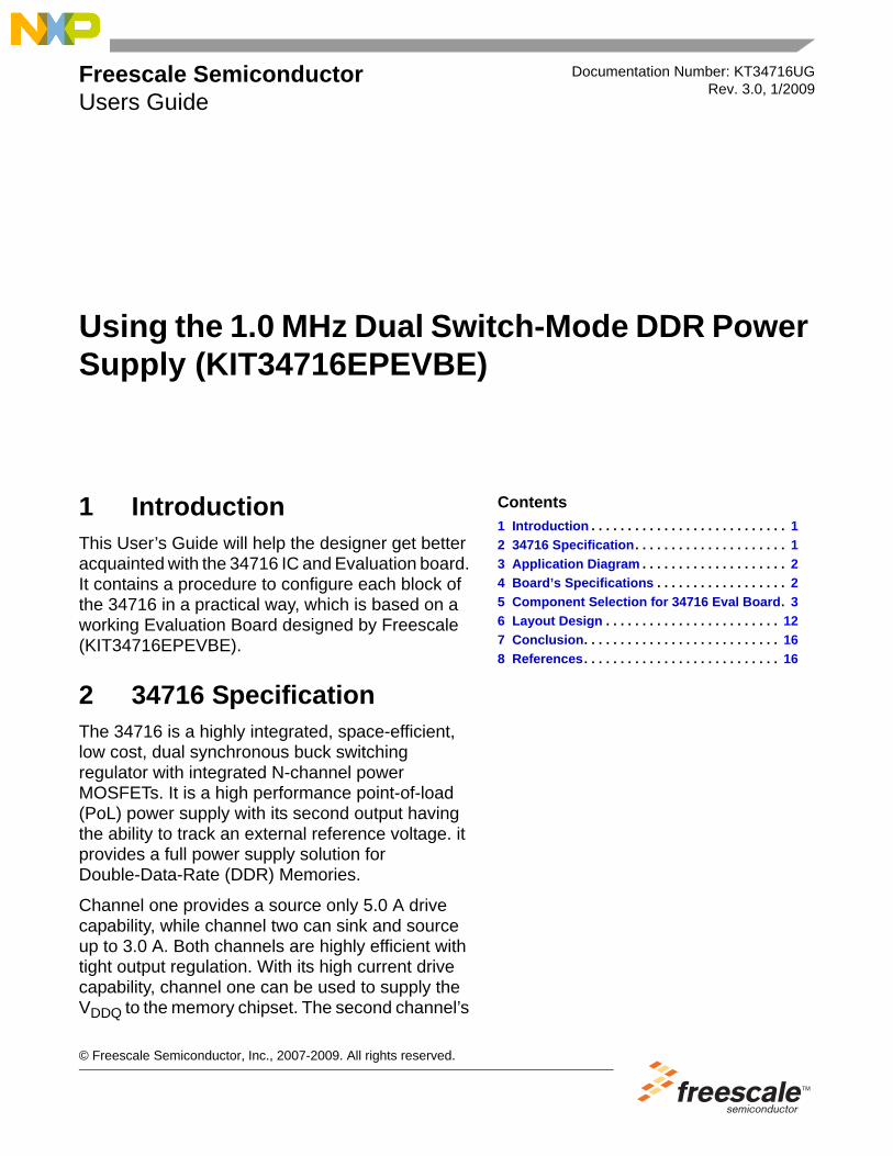
Freescale SemiconductorUsers Guide
Documentation Number: KT34716UGRev. 3.0, 1/2009
1 IntroductionThis User’s Guide will help the designer get better acquainted with the 34716 IC and Evaluation board. It contains a procedure to configure each block of the 34716 in a practical way, which is based on a working Evaluation Board designed by Freescale (KIT34716EPEVBE).
2 34716 SpecificationThe 34716 is a highly integrated, space-efficient, low cost, dual synchronous buck switching regulator with integrated N-channel power MOSFETs. It is a high performance point-of-load (PoL) power supply with its second output having the ability to track an external reference voltage. it provides a full power supply solution for Double-Data-Rate (DDR) Memories.
Channel one provides a source only 5.0 A drive capability, while channel two can sink and source up to 3.0 A. Both channels are highly efficient with tight output regulation. With its high current drive capability, channel one can be used to supply the VDDQ to the memory chipset. The second channel’s
Using the 1.0 MHz Dual Switch-Mode DDR Power Supply (KIT34716EPEVBE)
Contents1 Introduction . . . . . . . . . . . . . . . . . . . . . . . . . . . 12 34716 Specification. . . . . . . . . . . . . . . . . . . . . 13 Application Diagram . . . . . . . . . . . . . . . . . . . . 24 Board’s Specifications . . . . . . . . . . . . . . . . . . 25 Component Selection for 34716 Eval Board. 36 Layout Design . . . . . . . . . . . . . . . . . . . . . . . . 127 Conclusion. . . . . . . . . . . . . . . . . . . . . . . . . . . 168 References. . . . . . . . . . . . . . . . . . . . . . . . . . . 16
Using the 34716, Rev. 3.02 Freescale Semiconductor
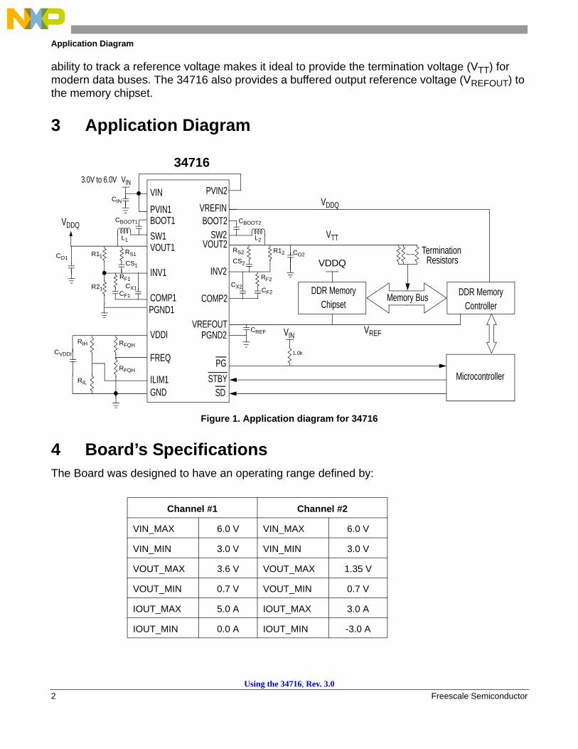
Application Diagram
ability to track a reference voltage makes it ideal to provide the termination voltage (VTT) for modern data buses. The 34716 also provides a buffered output reference voltage (VREFOUT) to the memory chipset.
3 Application Diagram
Figure 1. Application diagram for 34716
4 Board’s SpecificationsThe Board was designed to have an operating range defined by:
Channel #1 Channel #2
VIN_MAX 6.0 V VIN_MAX 6.0 V
VIN_MIN 3.0 V VIN_MIN 3.0 V
VOUT_MAX 3.6 V VOUT_MAX 1.35 V
VOUT_MIN 0.7 V VOUT_MIN 0.7 V
IOUT_MAX 5.0 A IOUT_MAX 3.0 A
IOUT_MIN 0.0 A IOUT_MIN -3.0 A
VINPVIN1
3.0V to 6.0V
BOOT1SW1
COMP1
VOUT1
VREFOUT
GND
VREFIN
VDDI
FREQ PGSTBY
SD
34716
Microcontroller
DDR MemoryController
DDR MemoryChipset
VIN
Memory Bus
TerminationVTT
VDDQ
VDDQ
VREF
PGND1
PVIN2
BOOT2SW2
INV2
COMP2
VOUT2
PGND2
VDDQ
ILIM1
INV1Resistors
VIN
CIN
CO1R11
R21
RS1
CS1
CBOOT1
L1
RF1
CF1
CVDDI
RIL
RIH RFQH
RFQH
CBOOT2
L2
RS2
CS2
R12 CO2
CX1 CX2
RF2
CF2
CREF
1.0k
Using the 34716, Rev. 3.0Freescale Semiconductor 3
Component Selection for 34716 Eval Board
5 Component Selection for 34716 Eval Board
5.1 I/O Parameters:VIN = PVIN1 = 3.3V
FSW = 1 MHz
VOUT1 = VDDQ= 1.8 V (DDR2 Standard)
IOUT1 = 5 A
PVIN2 = VREFIN =VOUT1=1.8V
VOUT2 =VTT = 0.90 V
IOUT2 = 3A
5.2 Configuring the Output Voltage:Channel 1 of the 34716 is a general purpose DC-DC converter, the resistor divider to the -INV1 node is the responsible for setting the output voltage. The equation is:
Where VREF is the internal VBG=0.7V.
Then, for a regulated output at 1.8 V, we choose R1 = 20KΩ and R2 is calculated as follows:
Channel 2 is a DDR specific voltage power supply, and the output voltage is given by the equation:
Where VREFIN is the VDDQ voltage supplied by VOUT1.
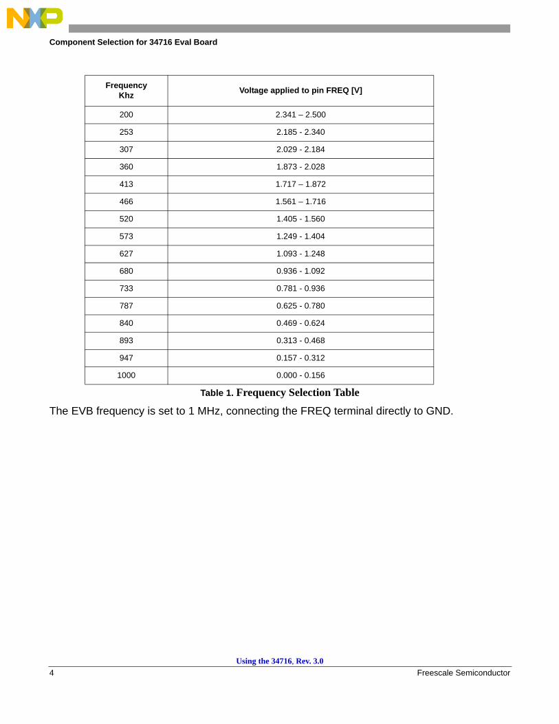
5.3 Switching Frequency ConfigurationThe switching frequency will have a value of 1.0 MHz by connecting the FREQ terminal to the GND terminal. If the smallest frequency value of 200 KHz is desired, then connect the FREQ terminal to VDDI. To program the switching frequency to another value, an external resistor divider will be connected to the FREQ terminal to achieve the voltages given by the Frequency Selection Table
⎟⎠⎞
⎜⎝⎛ += 1
21
RRVV REFOUT
Ω=−
= KVVRVR
REFOUT
REF 72.1212
2REFIN
TT
VV =
Using the 34716, Rev. 3.04 Freescale Semiconductor
Component Selection for 34716 Eval Board
Table 1. Frequency Selection Table
The EVB frequency is set to 1 MHz, connecting the FREQ terminal directly to GND.
FrequencyKhz Voltage applied to pin FREQ [V]
200 2.341 – 2.500
253 2.185 - 2.340
307 2.029 - 2.184
360 1.873 - 2.028
413 1.717 – 1.872
466 1.561 – 1.716
520 1.405 - 1.560
573 1.249 - 1.404
627 1.093 - 1.248
680 0.936 - 1.092
733 0.781 - 0.936
787 0.625 - 0.780
840 0.469 - 0.624
893 0.313 - 0.468
947 0.157 - 0.312
1000 0.000 - 0.156
Using the 34716, Rev. 3.0Freescale Semiconductor 5
Component Selection for 34716 Eval Board
5.4 Selecting InductorInductor calculation is as follows:
However, since channel 1 will be serving as power supply for channel 2, we have to locate the LC poles at different frequencies in order to ensure that the input impedance of the second converter is always higher than the output impedance of the first converter, and thus, ensure system stability. To move the LC poles, we can select different values of “L” for each channel, for instance, L1 = 1.0µH and L2 = 1.5µH, to allow some operating margin for each channel.
5.5 Input Capacitors for PVIN1 and PVIN2Input capacitor selection process is the same for both channels, and should be based on the current ripple allowed on the input line, since output of channel 1 is the input of channel 2, the input capacitor on channel 2 should be calculated for the maximum allowed output ripple on channel 1. The input capacitor should provide the ripple current generated during the inductor charge time. This ripple is dependent on the output current sourced by 34716 so that:
Where:
IRMS is the RMS value of the input capacitor current.
IOUT is the output current,
D= VOUT/Vin is the duty cycle.
For a buck converter, IRMS has its maximum at PVIN = 2VOUT
Maximum Off time percentage
Switching periodDrain – to – source resistance of FET
Winding resistance of Inductor
Output current ripple
sT µ1=
Ω= mlsonRds 45_)(
uHL 75.02 =uHL 72.01 =
OUT
OUTOUTMAX I
wrlsonRdsIVTDL∆
++∗∗=
))__)((*('
OUTOUT II *4.0=∆
max_1'
VinVD OUT
MAX −=
Ω= mwr 10_
)1( DDII OUTRMS −=
Using the 34716, Rev. 3.06 Freescale Semiconductor
Component Selection for 34716 Eval Board
Since
Where PMAX is the maximum power dissipation of the capacitor and is a constant based on physical size (generally given in the datasheets under the heading AC power dissipation.). We derive that the lower the ESR, the higher would be the ripple current capability. In other words, a low ESR capacitor (i.e., with high ripple current capability) can withstand high ripple current levels without overheating.
Therefore, for greater efficiency and because the overall voltage ripple on the input line also depends on the input capacitor ESR, we recommend using low ESR capacitors.
For a ∆VOUT = 0.5*Vin, Then CinMIN = 30.4µF
To ensure better performance on regulation, an array of low ESR ceramic capacitors were used to get a total of 300 µF in both input terminals.
5.6 Selecting the Output Filter CapacitorThe following considerations are most important for the output capacitor and not the actual Farad value: the physical size, the ESR of the capacitor, and the voltage rating.Calculate the minimum output capacitor using the following formula:
A more significative calculation must include the transient response in order to calculate the real minimum capacitor value and assure a good performance.
ESRPMAX=RMS_MAXI
VinVILCin
OUT
RMSMIN *
)(**5.0 2
∆=
VoutFIoutC
SW ∆∗∗∆
=80
Using the 34716, Rev. 3.0Freescale Semiconductor 7
Component Selection for 34716 Eval Board
.
As a DDR specification, the ESR should be around 2 mΩ. To achieve this, an array of capacitors in parallel were used, with 3 Low ESR Ceramic capacitors of 100 µF on each channel.
5.7 Bootstrap CapacitorFreescale recommends a 0.1 µF capacitor for CBOOT1 and CBOOT2.
5.8 Compensation NetworkCompensation network is calculated exactly in the same way for both channels. Since we are using different values for L, the LC poles will be located at different frequencies to ensure stability of the system when converter 1 is supplying the power voltage of converter 2.
1. Choose a value for R1 (May be equal for both channels)
2. Using a Crossover frequency of 100 kHz, set the Zero pole frequency to Fcross/10
3. Knowing the LC frequency, the Frequency of Zero 1 and Zero 2 in the compensation network are equal to FLC
Transient Response percentageMaximum Transient Voltage
Maximum current step
Inductor Current rise time
TR_%TR_V_dip = VOUT*TR_%
To find the Maximum allowed ESR, the following formula was used:
LFswDVoutVinstepIout
*max_*)min_(_ −
=∆
stepIoutIoutTriseIdt_
*__∆
=
dipVTRriseIdtIoutCo
____*
=
min)1(**
max DVoutLFswVoutESR
−∆
=
FP CR
FcrossF1
0 *21
101
π==
POF FR
C1*2
1π
=
FFZ CR
F*2
11 π
=S
Z CRF
12 *2
1π
=
1*21
ZFF FC
Rπ
=21*2
1
ZS FR
Cπ
=
2121
ZZXX
LC FFCoL
F ===π
Using the 34716, Rev. 3.08 Freescale Semiconductor
Component Selection for 34716 Eval Board
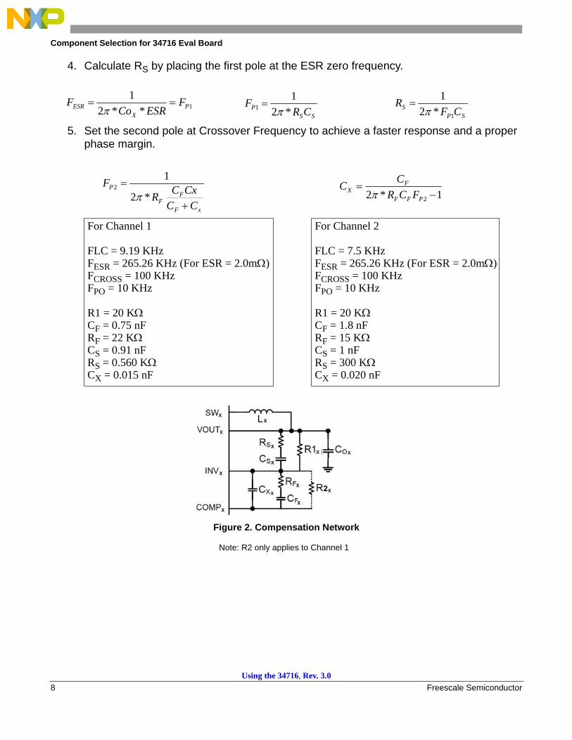
4. Calculate RS by placing the first pole at the ESR zero frequency.
5. Set the second pole at Crossover Frequency to achieve a faster response and a proper phase margin.
Figure 2. Compensation Network
Note: R2 only applies to Channel 1
SSP CR
F*21
1 π=
SPS CF
R1*2
1π
=1**21
PX
ESR FESRCo
F ==π
xF
FF
P
CCCxCR
F
+
=*2
12
π 1*2 2 −=
PFF
FX FCR
CCπ
For Channel 1
FLC = 9.19 KHzFESR = 265.26 KHz (For ESR = 2.0mΩ)FCROSS = 100 KHzFPO = 10 KHz
R1 = 20 KΩCF = 0.75 nFRF = 22 KΩCS = 0.91 nFRS = 0.560 KΩCX = 0.015 nF
For Channel 2
FLC = 7.5 KHzFESR = 265.26 KHz (For ESR = 2.0mΩ)FCROSS = 100 KHzFPO = 10 KHz
R1 = 20 KΩCF = 1.8 nFRF = 15 KΩCS = 1 nFRS = 300 KΩCX = 0.020 nF
Using the 34716, Rev. 3.0Freescale Semiconductor 9
Component Selection for 34716 Eval Board
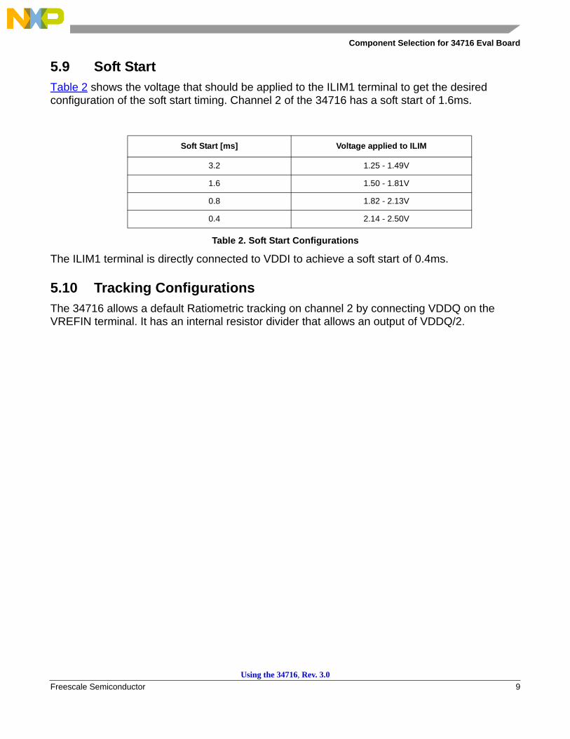
5.9 Soft StartTable 2 shows the voltage that should be applied to the ILIM1 terminal to get the desired configuration of the soft start timing. Channel 2 of the 34716 has a soft start of 1.6ms.
Table 2. Soft Start Configurations
The ILIM1 terminal is directly connected to VDDI to achieve a soft start of 0.4ms.
5.10 Tracking ConfigurationsThe 34716 allows a default Ratiometric tracking on channel 2 by connecting VDDQ on the VREFIN terminal. It has an internal resistor divider that allows an output of VDDQ/2.
Soft Start [ms] Voltage applied to ILIM
3.2 1.25 - 1.49V
1.6 1.50 - 1.81V
0.8 1.82 - 2.13V
0.4 2.14 - 2.50V
Using the 34716, Rev. 3.010 Freescale Semiconductor
Component Selection for 34716 Eval Board
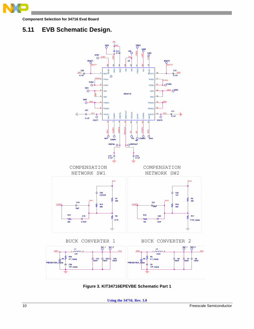
5.11 EVB Schematic Design.
Figure 3. KIT34716EPEVBE Schematic Part 1
BOOT2
INV1
COMP1
SW2
VO1
SW2
VR
EF
OU
T
VO2
INV2
COMP2
VO2
SW1 VO1
VD
DI
STBY
GND
VIN
FR
EQ
ILIM
2
ILIM
1
PG
SD
CO
MP
2
INV
2
VR
EF
IN
CO
MP
1
INV
1
PVIN2
SW2
PVIN1
BOOT1
SW1
GND
SW
1
GND
VO1 VO2
COMPENSATION
BUCK CONVERTER 1 BUCK CONVERTER 2
NETWORK SW1COMPENSATIONNETWORK SW2
VOUT2VOUT2
C22
1.8nF
C22
1.8nF
R420kR420k
C261nF_nopopC261nF_nopop
SW1SW1
C21
20pF
C21
20pF
Vo1_1Vo1_1
INV1INV1
R19
15k
R19
15k
GNDGND
C6100uF
C6100uF
C11
0.1uF
C11
0.1uF
R18300R18300
R34.7_nopopR34.7_nopop
C15
0.1uF
C15
0.1uF
R120kR120k
C120.1uFC120.1uF
PVIN1PVIN1
C18
15pF
C18
15pF
PGPG
R17
17.4k_nopop
R17
17.4k_nopop
D3
PMEG2010EA_nopop
D3
PMEG2010EA_nopop
VO2_2VO2_2
INV2INV2
FREQFREQ
D2
PMEG2010EA_nopop
D2
PMEG2010EA_nopop
VREFOUTVREFOUT
C140.1uFC140.1uF ILIM1ILIM1
Vo2_1Vo2_1
SDSD
C130.1uFC130.1uF
VINVIN
R15
22k
R15
22k
L1
1uH
L1
1uH
1 2
SW2SW2
R204.7_nopopR204.7_nopop
U2
MC34716
U2
MC34716
VIN
22
VIN
23
GN
D24
VD
DI
25
BOOT11
PGND14
SW13
PVIN12
SW13
PGND14
CO
MP
17
VR
EF
IN8
/SH
TD
11
VR
EF
OU
T9
/PG
OO
D10
CO
MP
212
PGND2 15
PGND2 15
SW2 16
SW2 16
FR
EQ
21
N/C
20
PVIN2 17
PVIN2 17
ST
BY
26
ILIM
119
BOOT2 18
VOUT2 14
INV
213
INV
16
VOUT15
PVIN12
COMP2COMP2
C25100uF
C25100uF
VREFINVREFIN
C91nF_nopopC91nF_nopop
C24100uF
C24100uF
C8100uF
C8100uF
BOOT1BOOT1
Vo1_2Vo1_2
C10100uF
C10100uF
C200.910nFC200.910nF
R14560R14560
VOUT1VOUT1
L2
1.5uH
L2
1.5uH
1 2
C27
0.1uF
C27
0.1uF
BOOT2BOOT2
PVIN2PVIN2
C7100uF
C7100uF
COMP1COMP1
STBYSTBY
ILIM2ILIM2
C231nFC231nF
VDDIVDDI
C19
0.75nF
C19
0.75nF
R2
12.7k
R2
12.7k
C28
0.1uF
C28
0.1uF
Using the 34716, Rev. 3.0Freescale Semiconductor 11
Component Selection for 34716 Eval Board
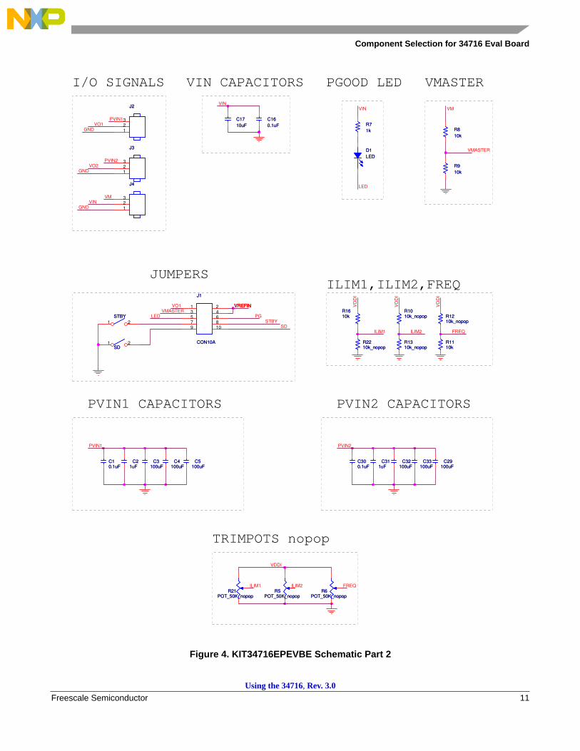
Figure 4. KIT34716EPEVBE Schematic Part 2
VREFINVREFIN
VIN
ILIM2 FREQ
PVIN1
GND
VIN
VO1
VDDI
PVIN1
PVIN2VO2
GND
VO1VMASTER
LEDSTBY
SDFREQILIM2
VM
PG
VMASTER
LED
VREFINVREFIN
ILIM1
VINGND
VD
DI
VD
DI
ILIM1
VD
DI
PVIN2
VM
I/O SIGNALS
JUMPERS
VIN CAPACITORS
PVIN1 CAPACITORS
TRIMPOTS nopop
PGOOD LED VMASTER
ILIM1,ILIM2,FREQ
PVIN2 CAPACITORS
J2J2
123
R1210k_nopopR1210k_nopop
R71kR71k
J3J3
123
R6POT_50K_nopop
R6POT_50K_nopop
R910kR910k
R5POT_50K_nopop
R5POT_50K_nopop
R1110kR1110k
C4100uF
C4100uF
D1LEDD1LED
STBYSTBY1 2
R2210k_nopopR2210k_nopop
R1610kR1610k
C5100uF
C5100uF
C33100uF
C33100uF
J1
CON10A
J1
CON10A
1 23 45 67 89 10
R21POT_50K_nopop
R21POT_50K_nopop
C29100uF
C29100uF
C32100uF
C32100uF
C21uF
C21uF
SDSD1 2
C311uF
C311uF
C300.1uFC300.1uF
C1710uFC1710uF
C3100uF
C3100uF
J4J4
123
C160.1uFC160.1uF
C10.1uFC10.1uF
R1310k_nopopR1310k_nopop
R810kR810k
R1010k_nopopR1010k_nopop
Using the 34716, Rev. 3.012 Freescale Semiconductor
Layout Design
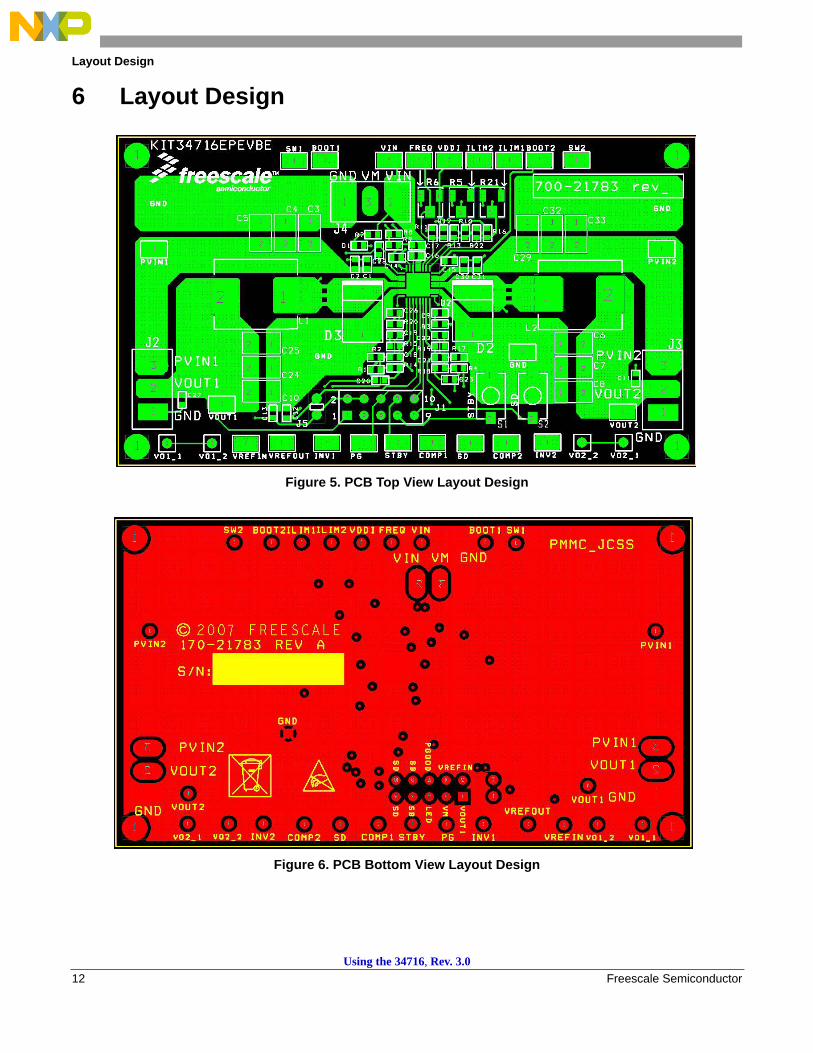
6 Layout Design
Figure 5. PCB Top View Layout Design
Figure 6. PCB Bottom View Layout Design
Using the 34716, Rev. 3.0Freescale Semiconductor 13
Layout Design
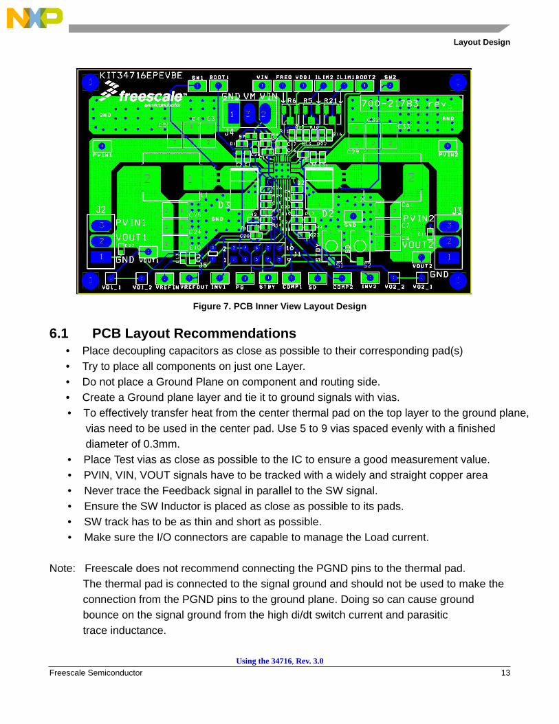
Figure 7. PCB Inner View Layout Design
6.1 PCB Layout Recommendations• Place decoupling capacitors as close as possible to their corresponding pad(s)• Try to place all components on just one Layer.• Do not place a Ground Plane on component and routing side.• Create a Ground plane layer and tie it to ground signals with vias.
• To effectively transfer heat from the center thermal pad on the top layer to the ground plane, vias need to be used in the center pad. Use 5 to 9 vias spaced evenly with a finished diameter of 0.3mm. • Place Test vias as close as possible to the IC to ensure a good measurement value. • PVIN, VIN, VOUT signals have to be tracked with a widely and straight copper area • Never trace the Feedback signal in parallel to the SW signal. • Ensure the SW Inductor is placed as close as possible to its pads. • SW track has to be as thin and short as possible. • Make sure the I/O connectors are capable to manage the Load current. Note: Freescale does not recommend connecting the PGND pins to the thermal pad. The thermal pad is connected to the signal ground and should not be used to make the connection from the PGND pins to the ground plane. Doing so can cause ground bounce on the signal ground from the high di/dt switch current and parasitic trace inductance.
Using the 34716, Rev. 3.014 Freescale Semiconductor
Layout Design
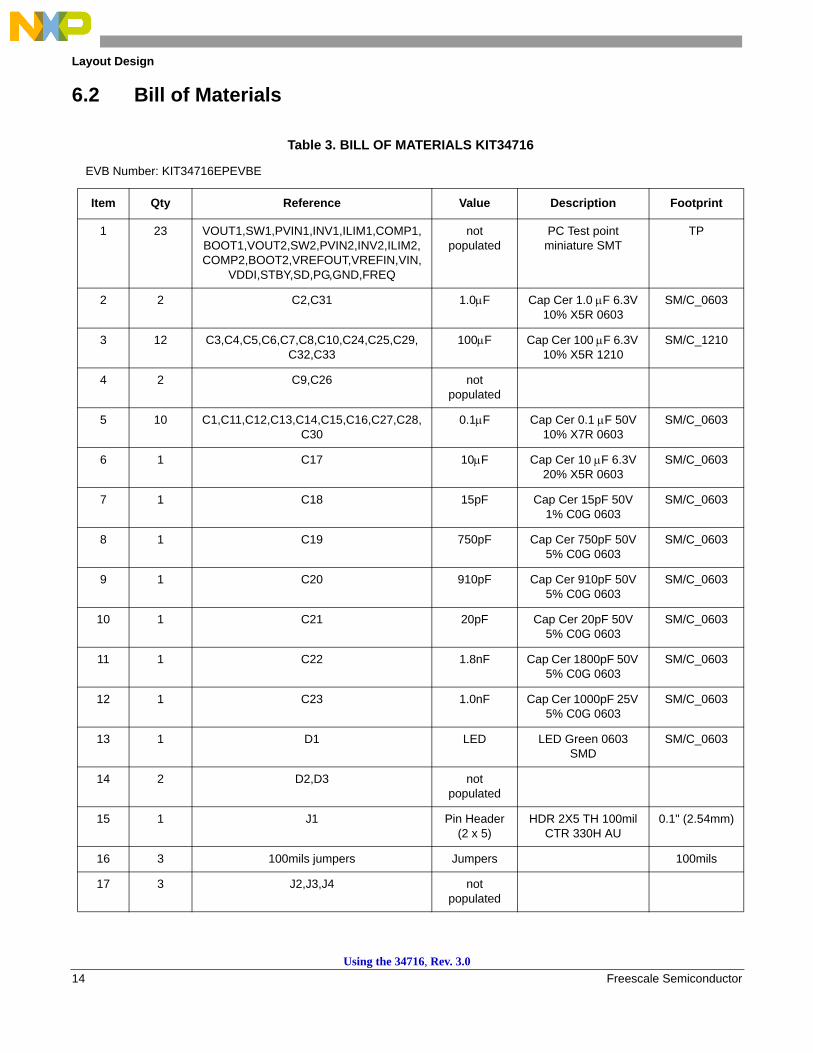
6.2 Bill of Materials
Table 3. BILL OF MATERIALS KIT34716
EVB Number: KIT34716EPEVBE
Item Qty Reference Value Description Footprint
1 23 VOUT1,SW1,PVIN1,INV1,ILIM1,COMP1,BOOT1,VOUT2,SW2,PVIN2,INV2,ILIM2,COMP2,BOOT2,VREFOUT,VREFIN,VIN,
VDDI,STBY,SD,PG,GND,FREQ
not populated
PC Test point miniature SMT
TP
2 2 C2,C31 1.0µF Cap Cer 1.0 µF 6.3V 10% X5R 0603
SM/C_0603
3 12 C3,C4,C5,C6,C7,C8,C10,C24,C25,C29,C32,C33
100µF Cap Cer 100 µF 6.3V 10% X5R 1210
SM/C_1210
4 2 C9,C26 not populated
5 10 C1,C11,C12,C13,C14,C15,C16,C27,C28,C30
0.1µF Cap Cer 0.1 µF 50V 10% X7R 0603
SM/C_0603
6 1 C17 10µF Cap Cer 10 µF 6.3V 20% X5R 0603
SM/C_0603
7 1 C18 15pF Cap Cer 15pF 50V 1% C0G 0603
SM/C_0603
8 1 C19 750pF Cap Cer 750pF 50V 5% C0G 0603
SM/C_0603
9 1 C20 910pF Cap Cer 910pF 50V 5% C0G 0603
SM/C_0603
10 1 C21 20pF Cap Cer 20pF 50V 5% C0G 0603
SM/C_0603
11 1 C22 1.8nF Cap Cer 1800pF 50V 5% C0G 0603
SM/C_0603
12 1 C23 1.0nF Cap Cer 1000pF 25V 5% C0G 0603
SM/C_0603
13 1 D1 LED LED Green 0603 SMD
SM/C_0603
14 2 D2,D3 not populated
15 1 J1 Pin Header (2 x 5)
HDR 2X5 TH 100mil CTR 330H AU
0.1" (2.54mm)
16 3 100mils jumpers Jumpers 100mils
17 3 J2,J3,J4 not populated
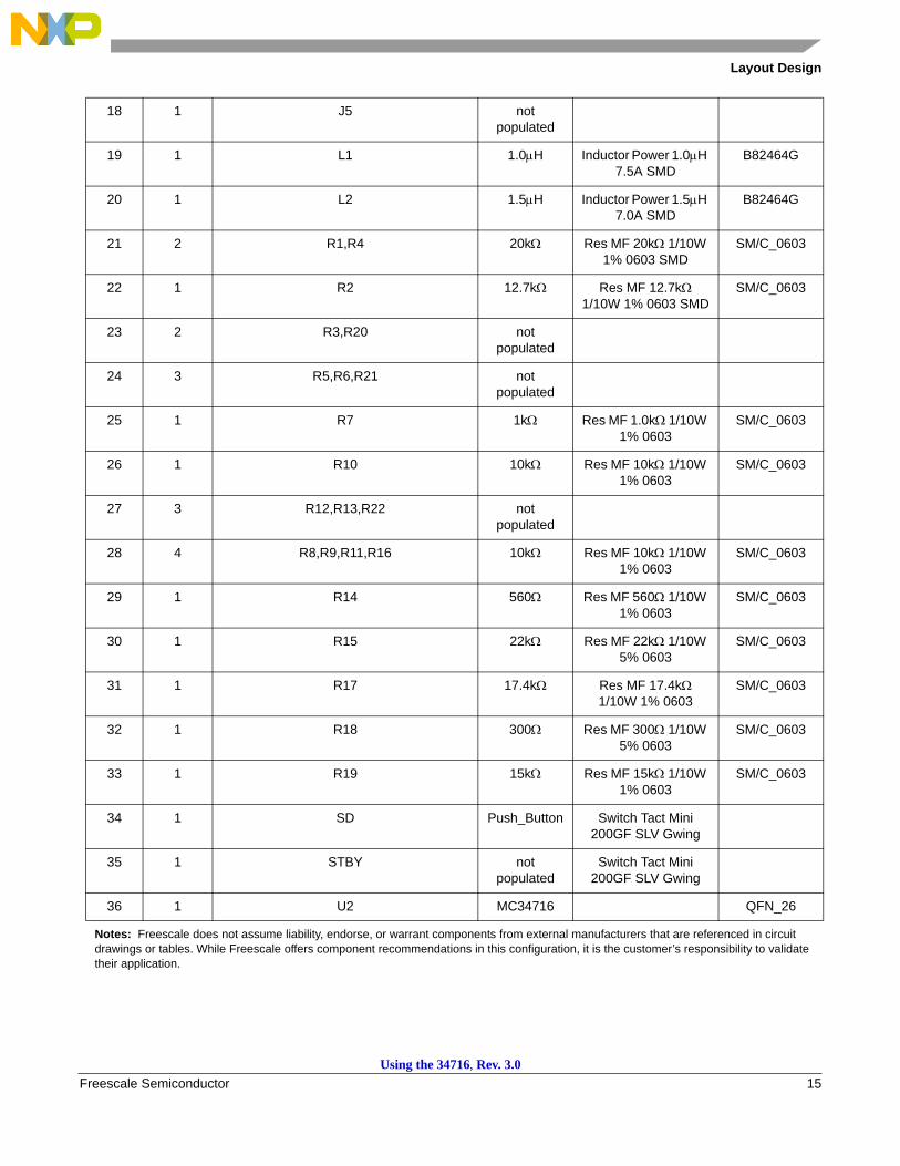
Using the 34716, Rev. 3.0Freescale Semiconductor 15
Layout Design
18 1 J5 not populated
19 1 L1 1.0µH Inductor Power 1.0µH 7.5A SMD
B82464G
20 1 L2 1.5µH Inductor Power 1.5µH 7.0A SMD
B82464G
21 2 R1,R4 20kΩ Res MF 20kΩ 1/10W 1% 0603 SMD
SM/C_0603
22 1 R2 12.7kΩ Res MF 12.7kΩ 1/10W 1% 0603 SMD
SM/C_0603
23 2 R3,R20 not populated
24 3 R5,R6,R21 not populated
25 1 R7 1kΩ Res MF 1.0kΩ 1/10W 1% 0603
SM/C_0603
26 1 R10 10kΩ Res MF 10kΩ 1/10W 1% 0603
SM/C_0603
27 3 R12,R13,R22 not populated
28 4 R8,R9,R11,R16 10kΩ Res MF 10kΩ 1/10W 1% 0603
SM/C_0603
29 1 R14 560Ω Res MF 560Ω 1/10W 1% 0603
SM/C_0603
30 1 R15 22kΩ Res MF 22kΩ 1/10W 5% 0603
SM/C_0603
31 1 R17 17.4kΩ Res MF 17.4kΩ 1/10W 1% 0603
SM/C_0603
32 1 R18 300Ω Res MF 300Ω 1/10W 5% 0603
SM/C_0603
33 1 R19 15kΩ Res MF 15kΩ 1/10W 1% 0603
SM/C_0603
34 1 SD Push_Button Switch Tact Mini 200GF SLV Gwing
35 1 STBY not populated
Switch Tact Mini 200GF SLV Gwing
36 1 U2 MC34716 QFN_26
Notes: Freescale does not assume liability, endorse, or warrant components from external manufacturers that are referenced in circuit drawings or tables. While Freescale offers component recommendations in this configuration, it is the customer’s responsibility to validate their application.
Using the 34716, Rev. 3.016 Freescale Semiconductor
Conclusion
7 ConclusionWith this User Guide, the user will be capable of configuring the 34716 as power supply for DDR memory chips, as well as other devices that can make use of some of the capabilities that the 34716 offers. The board is fully configured to work at any desirable input voltage within 3.0 and 6.0 V. However, it is highly recommended to calculate all components for the specific application situation in order to assure a better efficiency and stability of the IC.
8 References• 34716 Datasheet, 3A and 5A 1MHz Fully Integrated Double Switch-mode Power Supply,
Freescale Semiconductor, Inc.• Application Note “AN1989 MC34701 and MC34702 Component Selection Guide”,
Freescale Semiconductor, Inc.• Sanjaya Maniktala, “Switching Power Supplies A to Z”, Newnes, 2006.
How to Reach Us:
Home Page:www.freescale.com
Web Support:http://www.freescale.com/support
USA/Europe or Locations Not Listed:Freescale Semiconductor, Inc.Technical Information Center, EL5162100 East Elliot Road Tempe, Arizona 85284 +1-800-521-6274 or +1-480-768-2130www.freescale.com/support
Europe, Middle East, and Africa:Freescale Halbleiter Deutschland GmbHTechnical Information CenterSchatzbogen 781829 Muenchen, Germany+44 1296 380 456 (English)+46 8 52200080 (English)+49 89 92103 559 (German)+33 1 69 35 48 48 (French)www.freescale.com/support
Japan:Freescale Semiconductor Japan Ltd. Headquarters ARCO Tower 15F 1-8-1, Shimo-Meguro, Meguro-ku, Tokyo 153-0064Japan0120 191014 or +81 3 5437 [email protected]
Asia/Pacific:Freescale Semiconductor Hong Kong Ltd.Technical Information Center 2 Dai King Street Tai Po Industrial Estate Tai Po, N.T., Hong Kong +800 2666 [email protected]
For Literature Requests Only:Freescale Semiconductor Literature Distribution CenterP.O. Box 5405Denver, Colorado 802171-800-441-2447 or 303-675-2140Fax: [email protected]
KT34716UGRev. 3.01/2009
RoHS-compliant and/or Pb-free versions of Freescale products have the functionality and electrical characteristics of their non-RoHS-compliant and/or non-Pb-free counterparts. For further information, see http://www.freescale.com or contact your Freescale sales representative.
For information on Freescale’s Environmental Products program, go to http://www.freescale.com/epp.
Information in this document is provided solely to enable system and software implementers to use Freescale Semiconductor products. There are no express or implied copyright licenses granted hereunder to design or fabricate any integrated circuits or integrated circuits based on the information in this document.
Freescale Semiconductor reserves the right to make changes without further notice to any products herein. Freescale Semiconductor makes no warranty, representation or guarantee regarding the suitability of its products for any particular purpose, nor does Freescale Semiconductor assume any liability arising out of the application or use of any product or circuit, and specifically disclaims any and all liability, including without limitation consequential or incidental damages. “Typical” parameters that may be provided in Freescale Semiconductor data sheets and/or specifications can and do vary in different applications and actual performance may vary over time. All operating parameters, including “Typicals”, must be validated for each customer application by customer’s technical experts. Freescale Semiconductor does not convey any license under its patent rights nor the rights of others. Freescale Semiconductor products are not designed, intended, or authorized for use as components in systems intended for surgical implant into the body, or other applications intended to support or sustain life, or for any other application in which the failure of the Freescale Semiconductor product could create a situation where personal injury or death may occur. Should Buyer purchase or use Freescale Semiconductor products for any such unintended or unauthorized application, Buyer shall indemnify and hold Freescale Semiconductor and its officers, employees, subsidiaries, affiliates, and distributors harmless against all claims, costs, damages, and expenses, and reasonable attorney fees arising out of, directly or indirectly, any claim of personal injury or death associated with such unintended or unauthorized use, even if such claim alleges that Freescale Semiconductor was negligent regarding the design or manufacture of the part.
Freescale™ and the Freescale logo are trademarks of Freescale Semiconductor, Inc. All other product or service names are the property of their respective owners.
© Freescale Semiconductor, Inc., 2007-2009. All rights reserved.