Embed Size (px)
Citation preview
Application ReportSPMA073–July 2015
Using Feature Set of I2C Master on TM4C129xMicrocontrollers
AmitAshara
ABSTRACTThe inter-integrated circuit (I2C) is a multi-master, multi-slave, single-ended bus that is typically used forattaching lower speed peripheral ICs to processors and microcontrollers. The type of slave devices rangefrom non-volatile memory to data-acquisition devices like analog-to-digital converters (ADC), sensors, andso forth. This application report demonstrates how to use the feature rich I2C master on the TM4C129xmicrocontrollers to communicate with a host of slave devices in a system.
Project collateral and source code discussed in this document can be downloaded from the following URL:http://www.ti.com/lit/zip/spma073.
Contents1 Introduction ................................................................................................................... 22 Overview of I2C Protocol ................................................................................................... 23 Circuit Schematic for Example Code...................................................................................... 64 Basic I2C Controller Initialization .......................................................................................... 75 I2C Master Function: Interrupt, uDMA and FIFO Operation.......................................................... 146 TM4C129x I2C Glitch Filter Capability .................................................................................. 197 Conclusion .................................................................................................................. 208 References .................................................................................................................. 20
List of Figures
1 Open Drain Circuit ........................................................................................................... 22 Address Phase ACK......................................................................................................... 43 Address Phase NAK......................................................................................................... 44 Data Frame Write ............................................................................................................ 55 Data Frame Read............................................................................................................ 66 Circuit Schematic ............................................................................................................ 67 I2CMSA and Slave Address Representation ........................................................................... 118 I2C Transaction for I2C_MASTER_CMD_SINGLE_SEND ........................................................... 129 I2C Transaction for I2C_MASTER_CMD_BURST_SEND_START ................................................. 1210 I2C Transaction for I2C_MASTER_CMD_BURST_SEND_CONT................................................... 1311 I2C Transaction for I2C_MASTER_CMD_BURST_SEND_FINISH ................................................. 1312 I2C Transaction for I2C_MASTER_CMD_SINGLE_RECEIVE....................................................... 1313 I2C Transaction for I2C_MASTER_CMD_BURST_RECEIVE_START ............................................. 1314 I2C Transaction for I2C_MASTER_CMD_BURST_RECEIVE_CONT .............................................. 1415 I2C Transaction for I2C_MASTER_CMD_BURST_RECEIVE_FINISH ............................................. 1416 Transmit With CPU and Non FIFO....................................................................................... 1517 Receive With CPU and Non FIFO ....................................................................................... 1518 Transmit With CPU and FIFO ............................................................................................ 16
TivaWare is a trademark of Texas Instruments.All other trademarks are the property of their respective owners.
1SPMA073–July 2015 Using Feature Set of I2C Master on TM4C129x MicrocontrollersSubmit Documentation Feedback
Copyright © 2015, Texas Instruments Incorporated

Introduction www.ti.com
19 Receive With CPU and FIFO ............................................................................................. 1620 Transmit With uDMA and FIFO .......................................................................................... 1721 Receive With uDMA and FIFO ........................................................................................... 1722 Transmit in HS Mode ...................................................................................................... 1823 Receive in HS Mode ....................................................................................................... 1824 Glitch Filter v/s Baud Rate ................................................................................................ 20
1 IntroductionThe TM4C129x family of devices from Texas Instruments integrates up to 10 independent I2C moduleswith the following features:• I2C module with independent master and slave blocks on the same bus without requiring additional
pins for separate master and slave functions• Integrated 8-byte deep FIFO for transmit and receive operations that can be independently assigned to
either master or slave block• Efficient transfer mechanism using uDMA and FIFO that reduces CPU overhead during large data
transfers• Independent uDMA channel for Transmit and Receive operations• Programmable glitch suppression capability in terms of system clocks which meets the standard
requirements• Support for standard, fast, fast plus and high-speed mode through configurable timer register• Support for arbitration and clock stretching during master mode initiated transactions• Support for SMBus clock low timeout, dual-slave address and quick command features• Highly configurable interrupt mechanism to reduce dependency on polling mechanism
2 Overview of I2C ProtocolBefore the usage of I2C on the TM4C129x devices is described, it is important that some of the basicconcepts of the I2C protocol and bus are described first. This aids the understanding of the protocol andthe debugging issues on the physical bus using an oscilloscope or a logic analyzer.
The description is kept concise from the understanding perspective. For more information, see theUM10204: I2C-Bus Specification and User Manual.
2.1 Physical Layer of I2CThe I2C bus consists of two signals: serial clock (SCL) and serial data (SDA). At the IO level, both SCLand SDA are open-drain as shown in Figure 1.
Figure 1. Open Drain Circuit
2 Using Feature Set of I2C Master on TM4C129x Microcontrollers SPMA073–July 2015Submit Documentation Feedback
Copyright © 2015, Texas Instruments Incorporated

www.ti.com Overview of I2C Protocol
The output transistor drives low to create a logical 0 on the bus. The output transistor is off to float the pinto create a logical 1 on the bus. Hence, an external pull up to VDD is required. This is required since thebus is bidirectional; if one device on the bus transmits a logical 0 and another device transmits a logical 1,it will not create an electrical contention that could damage the IO. Instead a current path is establishedfrom the device transmitting a logical 1 to the device transmitting a logical 0 via the pull up resistor.
The important positive consequence of this are:• Multiple devices can place a different logical value and not damage the other devices due to excessive
current flow. It also has an effect on the workings of the I2C bus itself.• When this concept is applied to SCL, it provides the slave a mechanism for stretching the clock and
establishes a form of flow control.• When this concept is applied to SDA, it allows the master to detect another master, which is called bus
arbitration.
The important negative consequence of this is:• The rise time of the SCL and SDA are no longer a function of the drive strength but as defined by the
RC time constant, where R is the value of the pull-up resistor and C is the value of the parasitic andload capacitance on the bus. This limits the speed of operation.
• The speed of operation requires that the R value be decreased to reduce the RC time constant asparasitic and load capacitance cannot be changed readily, thereby, increasing the current via the Rwhen a logical 0 is applied from a device affecting the current drain on portable power devices.
2.2 Communication Layer of I2CThe I2C bus communicates using the timing of the SCL and SDA; however, there are some concepts thatneed to be defined first.• BUS IDLE: The idle state of a bus is defined when both SCL and SDA are high.• START BIT: The start bit of a I2C frame is defined as SDA driven low while SCL is high.• STOP BIT: The stop bit of an I2C frame is defined as SDA pulled high while SCL is high.
All bits are signaled between a start and stop bit. Any bit being transmitted by a device (master or slave) isSCL being pulled high and then driven low (pulsing) with the SDA kept at a steady state. It is illegal in I2Cfor the SDA to change when the SCL is high other than for a START or STOP bit.
Data is always exchanged in a 9-bit format, where 8-bits are used for data exchange and 1-bit is used foracknowledging the transmission by the receiver of the data. The receiver can be a master or a slave.
2.2.1 Address FrameThe first part of an I2C frame is called the address frame where the master presents a slave address. Theaddress frame is comprised of a 7-bit slave address, the 8th bit indicates the direction of transfer and the9th bit is used to acknowledge the transfer.
When the 8th bit is logical 0, the direction of data is from master to slave and is referred to as mastertransmit or write and when it is logical 1, the direction of data is from slave to master and is referred to asmaster receive or read.
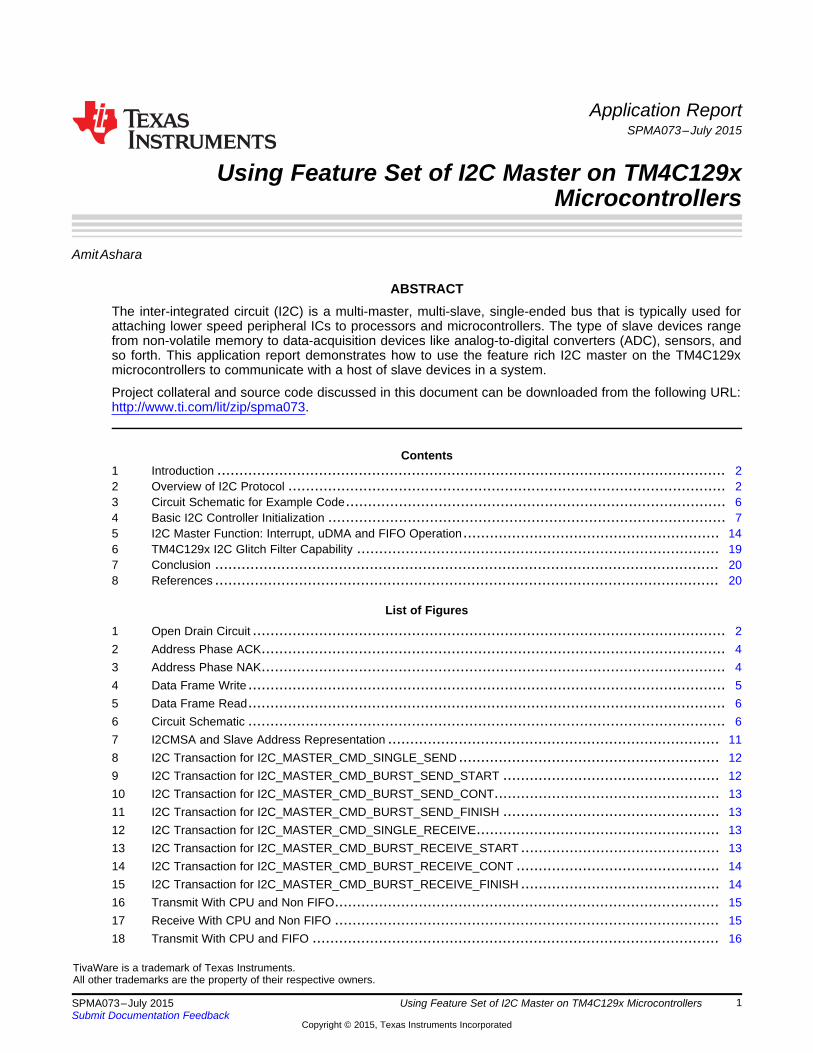
The 9th bit is called the acknowledge bit (ACK) and is used by the device receiving the data to indicate itis ready to accept the address. If the slave address exists on the bus, then the device corresponding to itshould drive the bus logical 0, which indicates to the master that it is ready to move to the data frame.
3SPMA073–July 2015 Using Feature Set of I2C Master on TM4C129x MicrocontrollersSubmit Documentation Feedback
Copyright © 2015, Texas Instruments Incorporated
Overview of I2C Protocol www.ti.com
Figure 2. Address Phase ACK
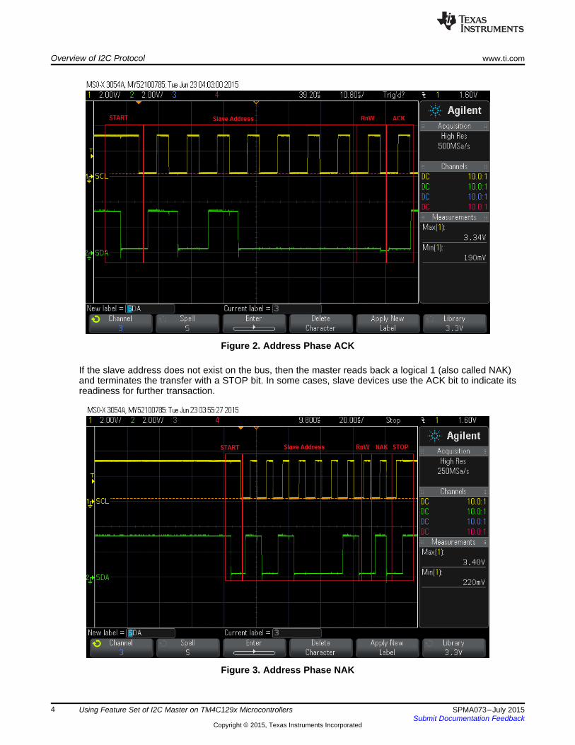
If the slave address does not exist on the bus, then the master reads back a logical 1 (also called NAK)and terminates the transfer with a STOP bit. In some cases, slave devices use the ACK bit to indicate itsreadiness for further transaction.
Figure 3. Address Phase NAK
4 Using Feature Set of I2C Master on TM4C129x Microcontrollers SPMA073–July 2015Submit Documentation Feedback
Copyright © 2015, Texas Instruments Incorporated

www.ti.com Overview of I2C Protocol
2.2.2 Data Frame WriteAfter the address frame, the next frame to be sent is the data frame (called a write operation) if a logical 0is sent in the 8th bit of the address frame. The direction of the transfer is from master to slave for the 8bits of data frame to follow. The 9th bit is the ACK bit for the data frame and the direction of this bit is fromslave to master. If the slave cannot accept the data, it should send a logical 1. The master should stop theI2C frame and the bus must return to idle state. If the slave accepts the data, it should send a logical 0and the master can send the next byte, stop the frame or change the direction of the bus using repeatedstart.
Figure 4. Data Frame Write
5SPMA073–July 2015 Using Feature Set of I2C Master on TM4C129x MicrocontrollersSubmit Documentation Feedback
Copyright © 2015, Texas Instruments Incorporated

Circuit Schematic for Example Code www.ti.com
2.2.3 Data Frame ReadAfter the address frame, the next frame to be sent is the data frame (called a read operation) if a logical 1is sent for the 8th bit in the address frame. The direction of the transfer is from slave to master for the 8bits of data. The 9th bit is the ACK bit for the data frame and the direction of this bit is from master toslave. If the master cannot accept the data, it should send a logical 1, the master should issue a STOPcondition on the I2C frame and the bus should return to idle state. If the master accepts the data, it shouldsend a logical 0 and the master can accept the next byte.
Figure 5. Data Frame Read
3 Circuit Schematic for Example CodeThis section discusses the schematic for the slave device (LAPIS semiconductor MR44V064A), which hasbeen used for development of the code examples. The slave device has been interfaced on the boosterpack header 1 on the EK-TM4C1294XL Connected Launchpad.
Figure 6. Circuit Schematic
6 Using Feature Set of I2C Master on TM4C129x Microcontrollers SPMA073–July 2015Submit Documentation Feedback
Copyright © 2015, Texas Instruments Incorporated

www.ti.com Basic I2C Controller Initialization
4 Basic I2C Controller Initialization
NOTE: The I2C controller initialization examples that have been described will use I2C moduleinstance 2 for the master function. Other I2C instances may be used but the user must referto the following section to ensure that the other instances are properly initialized.
To be able to use the I2C module on the TM4C129x family of devices, there are application peripheralinterfaces (API’s) that need to be called from the TivaWare™ software to correctly initialize the I2Cmodule on the TM4C129x devices.
There are two distinct sets of API’s that are required before any operation of the I2C controller for themaster function is configured:• Configuring the IO’s for I2C (see Section 4.1)• Configuring the I2C controller (master function) (see Section 4.2)
Once the initialization has been completed, only the I2C API can be called to perform data transfers fromthe master function for which the following operations are important:• Addressing a slave from the I2C master for transmit or receive operations (see Section 4.3)• Applying the correct command to the I2C master for transmit or receive operations (see Section 4.4)
7SPMA073–July 2015 Using Feature Set of I2C Master on TM4C129x MicrocontrollersSubmit Documentation Feedback
Copyright © 2015, Texas Instruments Incorporated

Basic I2C Controller Initialization www.ti.com
4.1 Configuration of IO’sThe first step of configuration is to enable and configure the GPIO corresponding to the I2C module’s SCLand SDA. The master and slave I2C modules are configured in the same manner. All I2C instances usethe same API for configuration, except for the parameters that need to be passed to the API which wouldbe instance specific.
Code Flow:• Enable the Clock to the corresponding GPIO Module using SysCtlPeripheralEnable and wait for the
peripheral ready using SysCtlPeripheralReady.• Call the GPIOPinConfigure API to configure the SCL and SDA port mux for the specific GPIO port and
pin.• Call the GPIOPinTypeI2C API to configure the SDA in open drain mode, digital enable and alternate
function select in the GPIO port for corresponding SDA pin.• Call the GPIOPinTypeI2CSCL API to configure the SCL for digital enable and alternate function select
in the GPIO port for the corresponding SCL pin. The open drain behavior is controlled by the I2Ccontroller; hence, it must not be set in the GPIO Open Drain Select Register (GPIOODR).
////Enable GPIO for Configuring the I2C Interface PinsSysCtlPeripheralEnable(SYSCTL_PERIPH_GPIOL);SysCtlPeripheralEnable(SYSCTL_PERIPH_GPIOK);
//// Wait for the Peripheral to be ready for programming//while(!SysCtlPeripheralReady(SYSCTL_PERIPH_GPIOL)
|| !SysCtlPeripheralReady(SYSCTL_PERIPH_GPIOK));
//// Configure Pins for I2C2 Master Interface//GPIOPinConfigure(GPIO_PL1_I2C2SCL);GPIOPinConfigure(GPIO_PL0_I2C2SDA);GPIOPinTypeI2C(GPIO_PORTL_BASE, GPIO_PIN_0);GPIOPinTypeI2CSCL(GPIO_PORTL_BASE, GPIO_PIN_1);
//// Configure Pins for I2C3 Slave Interface//GPIOPinConfigure(GPIO_PK4_I2C3SCL);GPIOPinConfigure(GPIO_PK5_I2C3SDA);GPIOPinTypeI2C(GPIO_PORTK_BASE, GPIO_PIN_5);GPIOPinTypeI2CSCL(GPIO_PORTL_BASE, GPIO_PIN_4);
8 Using Feature Set of I2C Master on TM4C129x Microcontrollers SPMA073–July 2015Submit Documentation Feedback
Copyright © 2015, Texas Instruments Incorporated

www.ti.com Basic I2C Controller Initialization
4.2 Configuring the I2C Controller (Master function)The next step is configuring the I2C controller master function. Traditional examples of the I2C controllerin TM4C have used the polling mechanism. This application report emphasizes the use of interruptsinstead of polling.
Code Flow:On TM4C129x device there is no System Control API to report the clock frequency.1. Use the SysCtlClockFreqSet API, or hard code a variable with the value of 16 MHz because the
default clock, after power up, is a 16 MHz precision oscillator (PIOSC). The clock frequency is requiredby the I2C API to compute the divider to generate the final I2C SCL clock frequency for differentmodes of operation.
2. Disable the clock, reset the I2C master module and then enable the clock to the I2C master moduleusing the SysCtlPeripheralDisable, SysCtlPeripheralReset and SysCtlPeripheralEnable APIs. Then,wait for the peripheral ready using SysCtlPeripheralReady. This step is required to ensure that anystale state of the bus or the master function (due to a previous run) is removed.
3. Call the I2CMasterInitExpClk API to configure the I2C master function for the correct SCL clockfrequency. The API uses the I2C base address as the first parameter, the system clock as the secondparameter and, based on true or false in the last parameter, configures the SCL clock frequency for100 KHz or 400 KHz. If the system clock is high enough to support high-speed mode, it will configurethe high-speed dividers as well.
4. Enable the interrupt sources by setting the corresponding bits in the I2C master function Interrupt MaskRegister. Use the I2CMasterIntEnableEx API, whose first parameter is the I2C base address and thenthe interrupt bits.
5. Enable the interrupt line from the I2C master function to the NVIC using the IntEnable API.//// Setup System Clock for 120MHz//ui32SysClock = SysCtlClockFreqSet((SYSCTL_OSC_MAIN | SYSCTL_USE_PLL | SYSCTL_XTAL_25MHZ |
SYSCTL_CFG_VCO_480), 120000000);
//// Stop the Clock, Reset and Enable I2C Module// in Master Function//SysCtlPeripheralDisable(SYSCTL_PERIPH_I2C2);SysCtlPeripheralReset(SYSCTL_PERIPH_I2C2);SysCtlPeripheralEnable(SYSCTL_PERIPH_I2C2);
//// Wait for the Peripheral to be ready for programming//while(!SysCtlPeripheralReady(SYSCTL_PERIPH_I2C2));
//// Initialize and Configure the Master Module//I2CMasterInitExpClk(I2C2_BASE, ui32SysClock, false);
//// Enable Interrupts for Arbitration Lost, Stop, NAK, Clock Low// Timeout and Data.//I2CMasterIntEnableEx(I2C2_BASE, (I2C_MASTER_INT_ARB_LOST |
I2C_MASTER_INT_STOP | I2C_MASTER_INT_NACK |I2C_MASTER_INT_TIMEOUT | I2C_MASTER_INT_DATA));
//// Enable the Interrupt in the NVIC from I2C Master//IntEnable(INT_I2C2);
9SPMA073–July 2015 Using Feature Set of I2C Master on TM4C129x MicrocontrollersSubmit Documentation Feedback
Copyright © 2015, Texas Instruments Incorporated

Basic I2C Controller Initialization www.ti.com
4.3 Addressing an I2C Slave in TM4C129xThe I2C master function uses the I2CMasterSlaveAddressSet API to set the address of the slave device.The first parameter is the I2C base address for the master function, the second parameter is the externalslave address (which is explained in detail using the example below) and the third parameter is thedirection of transfer. The third parameter is set to “true” for a read operation or “false” for a write operation.In the example below, a call of the function is shown to access a slave device with the slave address as0x50. Use Figure 7 to figure out the value.//*****************************************************************************//// Define for I2C Module////*****************************************************************************#define SLAVE_ADDRESS_EXT 0x50#define NUM_OF_I2CBYTES 255
// Send the Slave Address with RnW as Transmit// and First Data Byte. Based on Number of bytes the// command would be either START or FINISH//I2CMasterSlaveAddrSet(I2C2_BASE, SLAVE_ADDRESS_EXT, false);I2CMasterDataPut(I2C2_BASE, g_ui8MasterTxData[g_ui8MasterBytes++]);if(g_ui8MasterBytes == g_ui8MasterBytesLength){
I2CMasterControl(I2C2_BASE, I2C_MASTER_CMD_SINGLE_SEND);}else{
I2CMasterControl(I2C2_BASE, I2C_MASTER_CMD_BURST_SEND_START);}
}
The top part of Figure 7 shows the address phase as expected by the external slave device for which itwould ACK the address phase, and the bottom part shows the I2C Master Slave Address Register(I2CMSA) information from the Tiva™ TM4C1294NCPDT Microcontroller Data Sheet (SPMS433). The bitsshown as A2, A1 and A0 are based on the tie off done for the slave device pins, which are connected toGND. Therefore, the binary address as expected by the slave device is 1010000. This sequence inhexadecimal format is 0x50.
In the TM4C129x I2CMSA register, the address bits appear in bit position 7 to 1. TheI2CMasterSlaveAddressSet API takes care of shifting the slave address to the correct position in theregister.
10 Using Feature Set of I2C Master on TM4C129x Microcontrollers SPMA073–July 2015Submit Documentation Feedback
Copyright © 2015, Texas Instruments Incorporated

1 2 3 4 5 6 7 8 9 1 2
1 0 1 0 A2 A1 A0 R/W
SCL
SDA
StartCondition
ACK
31 30 29 28 27 26 25 24 23 22 21 20 19 18 17 16
14 13 12 11 10 9 8 7 6 5 4 3 2 1 015
RO0
RO0
RO0
RO0
RO0
RO0
RO0
RO0
RO0
RO0
RO0
RO0
RO0
RO0
RO0
RO0
RO0
RO0
RO0
RO0
RO0
RO0
RO0
RO0
RW0
RW0
RW0
RW0
RW0
RW0
RW0
RW0
TypeReset
TypeReset
Bit/Field Name Type Reset Description
Software should not rely on the value of a reserved bit. To providecompatibility with future products, the value of a reserved bit should bepreserved across a read-modify-write operation.
I C Slave Address2
This field specifies bits A6 through A0 of the slave address.
Receive/Send
The R/S bit specifies if the next master operation is a Receive (High)or Transmit (Low).
Value Description
0 Transmit
1 Receive
31:8
7:1
0
Reserved
SA
R/S
RO
RW
RW
0x00
0
0x0000.00
R/S
Reserved
Reserved SA
www.ti.com Basic I2C Controller Initialization
Figure 7. I2CMSA and Slave Address Representation
4.4 Data Transfer Commands for I2C Master in TM4C129xThe I2C master has two modes of operation. In the first mode of operation the CPU or DMA can use theI2C Master Data Register (I2CMDR) to write data to a slave or read data from a slave using a single bytebuffer. While the absolute address of the I2CMDR is programmed in the control structure of uDMA, for theCPU to access the data register there are two APIs that are available.• I2CDataPut is used to write data to a slave during a transmit operation. The API expects the first
parameter as the I2C base address and the second parameter is the data that must be transmitted• I2CDataGet is used to read data from a slave during a receive operation. The API expects the first
parameter as the I2C base address and returns the data read from the I2CMDR register.
The example codes of ektm4c129_i2c_master_cpu_nonfifo (see Section 5.1) andektm4c129_i2c_master_hs (see Section 5.4) uses the first mode of data transfer.
The second mode of operation uses the I2C FIFO Data Register (I2CFIFODATA) to write data to a slaveor read data from a slave using the FIFO. As with the first mode, the absolute address of theI2CFIFODATA is programmed in the control structure of the uDMA for DMA based transfers. For the CPUto access the data register, there are four APIs that are available.• I2CFIFODataPut is used to write data to the TX FIFO in blocking mode. The API uses the first
parameter of the I2C base address to polls the corresponding I2C FIFO Status Register(I2CFIFOSTATUS) to see if there is space available in the TX FIFO; if at least one byte space isavailable, the data then writes the second parameter to the I2CFIFODATA register.
11SPMA073–July 2015 Using Feature Set of I2C Master on TM4C129x MicrocontrollersSubmit Documentation Feedback
Copyright © 2015, Texas Instruments Incorporated

Basic I2C Controller Initialization www.ti.com
• I2CFIFODataPutNonBlocking is used to write data to the TX FIFO in non-blocking mode. The API usesthe first parameter of the I2C base address to check the corresponding I2CFIFOSTATUS register tosee if there is space available in the TX FIFO and writes the second parameter to the I2CFIFODATAregister. The API returns a ‘0’ if there is no space available (so it can be retried at a later time) or itreturns a ‘1’ if the space was available and the data was written to the I2CFIFODATA register.
• I2CFIFODataGet is used to read data from the RX FIFO in blocking mode. The API uses the firstparameter of the I2C base address to poll the corresponding I2CFIFOSTATUS register to see if thereis data available in the RX FIFO; if at least one byte is available for read, the data is returned by thefunction.
• I2CFIFODataGetNonBlocking is used to read data from the RX FIFO in non-blocking mode. The APIuses the first parameter of the I2C base address to check the corresponding I2CFIFOSTATUS registerto see if there is data available in the RX FIFO, and writes the data read from the I2CFIFODATA intothe buffer pointed by the second parameter. The API returns a ‘0’ if there is no data available (so it canbe retried at a later time) or returns a ‘1’ if the data was available and was read from theI2CFIFODATA register.
The example codes of ektm4c129_i2c_master_cpu_fifo (see Section 5.2) use the second mode of datatransfer in non-blocking mode.
4.5 Commanding Operation of the I2C MasterThe I2C master function uses the I2C Master Control/Status Register (I2CMCS) for performing any bustransaction. This register is a write-only register and read of this register will return the status of the I2Cmaster function. Thus, if a user writes to the register in the application code, it will not read back the lastcommand for the I2C master function but the status of the I2C master function resulting from the same.
The i2c.h file defines the different commands that can be sent to the I2C master function. From anapplication code perspective, there are eight major commands that the application can use to control thenature of the transaction from the I2C master.
4.5.1 I2C Transmit Command: I2C_MASTER_CMD_SINGLE_SENDThis command is used when the I2C master function is required to write one byte of data to a slave. Asshown in Figure 8 when the I2C_MASTER_CMD_SINGLE_SEND command is sent, the I2C masterfunction sends the start bit (S), slave address of 0x50 with Write Bit clear, transmits the data written to theI2CMDR and sends the stop bit (P).
Figure 8. I2C Transaction for I2C_MASTER_CMD_SINGLE_SEND
4.5.2 I2C Transmit Command: I2C_MASTER_CMD_BURST_SEND_STARTThis command is used when the I2C master function is required to write one byte of data to a slave andown the bus. As shown in Figure 9 when the I2C_MASTER_CMD_BURST_SEND_START command issent, the I2C master function sends the start bit (S), slave address of 0x50 with Write Bit clear, transmitsthe data written to the I2CMDR and holds the bus low for further operations.
Figure 9. I2C Transaction for I2C_MASTER_CMD_BURST_SEND_START
12 Using Feature Set of I2C Master on TM4C129x Microcontrollers SPMA073–July 2015Submit Documentation Feedback
Copyright © 2015, Texas Instruments Incorporated

www.ti.com Basic I2C Controller Initialization
4.5.3 I2C Transmit Command: I2C_MASTER_CMD_BURST_SEND_CONTThis command is used when the I2C master function is required to an additional byte of data to a slavewhen it owns the bus. As shown in Figure 10 when the I2C_MASTER_CMD_BURST_SEND_CONTcommand is sent, the I2C master function transmits the data written to the I2CMDR and holds the bus lowfor further operations.
Figure 10. I2C Transaction for I2C_MASTER_CMD_BURST_SEND_CONT
4.5.4 I2C Transmit Command: I2C_MASTER_CMD_BURST_SEND_FINISHThis command is used when the I2C master function is required to write one byte of data to a slave andrelease the bus. As shown in Figure 11 when the I2C_MASTER_CMD_BURST_SEND_FINISH commandis sent, the I2C master function transmits the data written to the I2CMDR and sends the stop bit (P).
Figure 11. I2C Transaction for I2C_MASTER_CMD_BURST_SEND_FINISH
4.5.5 I2C Receive Command: I2C_MASTER_CMD_SINGLE_RECEIVEThis command is used when the I2C master function is required to read one byte of data from a slave. Asshown in Figure 12 when the I2C_MASTER_CMD_SINGLE_RECEIVE command is sent, the I2C masterfunction sends the start bit (S), sets the slave address of 0x50 with Write Bit, receives the data from theslave, writes it to the I2CMDR, asserts a NAK to indicate to the slave that the transaction is completed andsends the stop bit (P).
Figure 12. I2C Transaction for I2C_MASTER_CMD_SINGLE_RECEIVE
4.5.6 I2C Receive Command: I2C_MASTER_CMD_BURST_RECEIVE_STARTThis command is used when the I2C master function is required to read one byte of data from a slave andown the bus. As shown in Figure 13 when the I2C_MASTER_CMD_BURST_RECEIVE_START commandis sent, the I2C master function sends the start bit (S), sets the slave address of 0x50 with Write Bit,receives the data from the slave, sends the data byte for ACK, writes the data to the I2CMDR and holdsthe bus for further operations.
Figure 13. I2C Transaction for I2C_MASTER_CMD_BURST_RECEIVE_START
13SPMA073–July 2015 Using Feature Set of I2C Master on TM4C129x MicrocontrollersSubmit Documentation Feedback
Copyright © 2015, Texas Instruments Incorporated

I2C Master Function: Interrupt, uDMA and FIFO Operation www.ti.com
4.5.7 I2C Receive Command: I2C_MASTER_CMD_BURST_RECEIVE_CONTThis command is used when the I2C master function is required to read one byte of data from a slavewhen it owns the bus. As shown in Figure 14 when the I2C_MASTER_CMD_BURST_RECEIVE_CONTcommand is sent, the I2C master function receives the data from the slave, sends ACK for the data byte,writes it to the I2CMDR and holds the bus for further operations.
Figure 14. I2C Transaction for I2C_MASTER_CMD_BURST_RECEIVE_CONT
4.5.8 I2C Receive Command: I2C_MASTER_CMD_BURST_RECEIVE_FINISHThis command is used when the I2C master function is required to read one byte of data from a slavewhen it owns the bus and then release the bus. As shown in Figure 15 when theI2C_MASTER_CMD_BURST_RECEIVE_FINISH command is sent, the I2C master receives the data fromthe slave, sends a NAK to indicate that the transaction has completed and sends the stop bit (P).
Figure 15. I2C Transaction for I2C_MASTER_CMD_BURST_RECEIVE_FINISH
5 I2C Master Function: Interrupt, uDMA and FIFO OperationThe I2C master supports both the polling and interrupt driven mechanisms for performing bustransactions. While the polling mechanism is simpler, the action of polling requires precious CPU cyclesperforming status checks. The TM4C129x family of devices now supports an exhaustive interruptmechanism that an application code may use to free precious CPU clocks for other device activities.
The TM4C129x family of devices includes an 8-byte deep transmit and receive FIFO with configurabletrigger threshold. The FIFO enables the CPU to setup a bulk transfer with fewer interrupts per I2Ctransactions leaving the CPU for other device activities.
The FIFO can be coupled with the efficient uDMA so that the CPU can be notified of a transactioncompletion, thus, reducing the overall CPU clocks managing a data transaction.
The code examples in the following subsections illustrate each of the features so that the applicationdeveloper can leverage the I2C features of the TM4C129x devices for improving overall CPU bandwidthfor essential system functions.
Each of the code examples mentioned below have logic analyzer captures associated with them, whichshows both transmit and receive plots. The plot contains the SCL and SDA IO for the I2C master functionand a GPIO toggle for interrupt, which is made high when the interrupt handler is called and made low onexit.
14 Using Feature Set of I2C Master on TM4C129x Microcontrollers SPMA073–July 2015Submit Documentation Feedback
Copyright © 2015, Texas Instruments Incorporated

www.ti.com I2C Master Function: Interrupt, uDMA and FIFO Operation
5.1 Master Function for CPU With Non-FIFO Transactionektm4c129_i2c_master_cpu_nonfifo is a simple code example in which the CPU uses the traditionalI2CMDR to access the slave for write and read operations with interrupts.
Figure 16 and Figure 17 show the transmit and receive operations. As can be seen for every datatransaction, the CPU is being interrupted.
Figure 16. Transmit With CPU and Non FIFO
Figure 17. Receive With CPU and Non FIFO
15SPMA073–July 2015 Using Feature Set of I2C Master on TM4C129x MicrocontrollersSubmit Documentation Feedback
Copyright © 2015, Texas Instruments Incorporated

I2C Master Function: Interrupt, uDMA and FIFO Operation www.ti.com
5.2 Master Function for CPU With FIFOektm4c129_i2c_master_cpu_fifo is a simple code example in which the CPU uses the I2CFIFODATA toaccess transmit and receive FIFO to perform write and read operations to a slave with interrupts.
Figure 18 and Figure 19 show the transmit and receive operations. As can be seen, the CPU is now beinginterrupted less than before; during the interrupt, the CPU can write or read the threshold of the data tothe FIFO. However, this is still suboptimal as the buffer management has to be done by the CPU.
Figure 18. Transmit With CPU and FIFO
Figure 19. Receive With CPU and FIFO
16 Using Feature Set of I2C Master on TM4C129x Microcontrollers SPMA073–July 2015Submit Documentation Feedback
Copyright © 2015, Texas Instruments Incorporated

www.ti.com I2C Master Function: Interrupt, uDMA and FIFO Operation
5.3 Master Function for uDMA With FIFOektm4c129_i2c_master_udma_fifo is a simple code example where the CPU initializes and configures theuDMA to use the I2CFIFODATA to access transmit and receive FIFO to perform write and read operationsto a slave with interrupt for the CPU on bus transaction completion. An important consideration in the codeis setting the arbitration size of the uDMA based on the threshold of the FIFO triggers. The code itself hasthe optimal settings for the arbitration size as per the threshold of the TX and RX FIFOs.
Figure 20 and Figure 21 show the transmit and receive operations. As can be seen, the CPU is now beinginterrupted only when the data transfer is completed by the uDMA and for handling bus events. This is anoptimal usage of the FIFO when the uDMA performs the buffer management and only informing the CPUof a transaction completion.
Figure 20. Transmit With uDMA and FIFO
Figure 21. Receive With uDMA and FIFO
17SPMA073–July 2015 Using Feature Set of I2C Master on TM4C129x MicrocontrollersSubmit Documentation Feedback
Copyright © 2015, Texas Instruments Incorporated

I2C Master Function: Interrupt, uDMA and FIFO Operation www.ti.com
5.4 Master Function for High-Speed Operationektm4c129_i2c_master_hs is a simple code example where the CPU uses the traditional I2CMDR toaccess the slave for write and read operations with interrupts. The main transactions in this example areperformed in high-speed mode reducing the overall time spent by the CPU for write and read bustransactions.
For both transmit and receive, Figure 22 shows the entire transmission and Figure 23 shows the zoomedin version with the baud rate for high speed.
Note that just like the other examples of using FIFO, CPU bandwidth for performing other system taskscan be improved while reducing the overall transaction time for the I2C bus transaction.
Figure 22. Transmit in HS Mode
Figure 23. Receive in HS Mode
18 Using Feature Set of I2C Master on TM4C129x Microcontrollers SPMA073–July 2015Submit Documentation Feedback
Copyright © 2015, Texas Instruments Incorporated

www.ti.com TM4C129x I2C Glitch Filter Capability
6 TM4C129x I2C Glitch Filter CapabilityAn important feature on the TM4C12x device is the I2C glitch filter that allows the application code torobustly handle transient noises that may affect the master. This feature is applicable for both the masterand slave function of the TM4C12x devices. The major difference of this function on the TM4C129x whencompared to the TM4C123x family of the devices is that the feature is enabled or disabled without havingthe requirement to set or clear control bit.
The I2C specification requirement for glitch suppression is 50 ns for standard (fast and fast plus mode)and 10 ns for high speed mode. The TM4C129x glitch filters work on the system clock and, based on thesystem clock frequency, the value assigned to the filter must be adjusted to the nearest available setting inthe glitch filter register I2C Master Timer Period Register (I2CMTPR). For example, if the system clock is120 MHz (8.33 ns), then for the standard mode glitch suppression of 50 ns would be a value of 6 systemclocks. The nearest available value is 8 system clocks. Similarly for high-speed mode, a glitchsuppression of 10 ns would be 1.2 system clocks, for which the value of 2 has to be programmed in theI2CMTPR.
The I2C glitch filter on the TM4C129x devices uses the API I2CMasterGlitchFilterConfigSet. The firstparameter for the API is the base address of the I2C module and the second parameter is the filter setting.By setting the value of the filter as 0 (I2C_MASTER_GLITCH_FILTER_DISABLED), the glitch filter isautomatically disabled.//// Enable the Glitch Filter. Writting a value 0 will// disable the glitch filter// I2C_MASTER_GLITCH_FILTER_DISABLED// I2C_MASTER_GLITCH_FILTER_1// I2C_MASTER_GLITCH_FILTER_2 : Ideal Value when in HS Mode// for 120MHz clock// I2C_MASTER_GLITCH_FILTER_4// I2C_MASTER_GLITCH_FILTER_8 : Ideal Value when in Std,// Fast, Fast+ for 120MHz clock// I2C_MASTER_GLITCH_FILTER_16// I2C_MASTER_GLITCH_FILTER_32//I2CMasterGlitchFilterConfigSet(I2C2_BASE, I2C_MASTER_GLITCH_FILTER_8);
19SPMA073–July 2015 Using Feature Set of I2C Master on TM4C129x MicrocontrollersSubmit Documentation Feedback
Copyright © 2015, Texas Instruments Incorporated

Conclusion www.ti.com
However, the I2C glitch filter on the TM4C129x has an effect on the baud rate. Figure 24 shows the actualbaud rate for a system clock of 120 MHz and 16 MHz when the device is programmed for 100 KHzoperation. This can be compensated by overriding the TPR value in the I2CMTPR register after theinitialization API's have been called.
Figure 24. Glitch Filter v/s Baud Rate
7 ConclusionThe new features of FIFO and uDMA for the I2C controller allow you to substantially improve theperformance of the application in terms of CPU execution cycle allocation to the other system tasks, whileensuring that the I2C, in conjunction with the uDMA and FIFO, have better management of the data andcontrol transfer from the peripheral devices in the end system.
8 References• Tiva™ TM4C1294NCPDT Microcontroller Data Sheet (SPMS433)• UM10204: I2C-Bus Specification and User Manual• TivaWare software• MR44V064A 64k (8,192-Word × 8-Bit) Ferroelectric Random Access Memory (FeRAM) Data Sheet -
LAPIS Semiconductor
20 Using Feature Set of I2C Master on TM4C129x Microcontrollers SPMA073–July 2015Submit Documentation Feedback
Copyright © 2015, Texas Instruments Incorporated

IMPORTANT NOTICE
Texas Instruments Incorporated and its subsidiaries (TI) reserve the right to make corrections, enhancements, improvements and otherchanges to its semiconductor products and services per JESD46, latest issue, and to discontinue any product or service per JESD48, latestissue. Buyers should obtain the latest relevant information before placing orders and should verify that such information is current andcomplete. All semiconductor products (also referred to herein as “components”) are sold subject to TI’s terms and conditions of salesupplied at the time of order acknowledgment.TI warrants performance of its components to the specifications applicable at the time of sale, in accordance with the warranty in TI’s termsand conditions of sale of semiconductor products. Testing and other quality control techniques are used to the extent TI deems necessaryto support this warranty. Except where mandated by applicable law, testing of all parameters of each component is not necessarilyperformed.TI assumes no liability for applications assistance or the design of Buyers’ products. Buyers are responsible for their products andapplications using TI components. To minimize the risks associated with Buyers’ products and applications, Buyers should provideadequate design and operating safeguards.TI does not warrant or represent that any license, either express or implied, is granted under any patent right, copyright, mask work right, orother intellectual property right relating to any combination, machine, or process in which TI components or services are used. Informationpublished by TI regarding third-party products or services does not constitute a license to use such products or services or a warranty orendorsement thereof. Use of such information may require a license from a third party under the patents or other intellectual property of thethird party, or a license from TI under the patents or other intellectual property of TI.Reproduction of significant portions of TI information in TI data books or data sheets is permissible only if reproduction is without alterationand is accompanied by all associated warranties, conditions, limitations, and notices. TI is not responsible or liable for such altereddocumentation. Information of third parties may be subject to additional restrictions.Resale of TI components or services with statements different from or beyond the parameters stated by TI for that component or servicevoids all express and any implied warranties for the associated TI component or service and is an unfair and deceptive business practice.TI is not responsible or liable for any such statements.Buyer acknowledges and agrees that it is solely responsible for compliance with all legal, regulatory and safety-related requirementsconcerning its products, and any use of TI components in its applications, notwithstanding any applications-related information or supportthat may be provided by TI. Buyer represents and agrees that it has all the necessary expertise to create and implement safeguards whichanticipate dangerous consequences of failures, monitor failures and their consequences, lessen the likelihood of failures that might causeharm and take appropriate remedial actions. Buyer will fully indemnify TI and its representatives against any damages arising out of the useof any TI components in safety-critical applications.In some cases, TI components may be promoted specifically to facilitate safety-related applications. With such components, TI’s goal is tohelp enable customers to design and create their own end-product solutions that meet applicable functional safety standards andrequirements. Nonetheless, such components are subject to these terms.No TI components are authorized for use in FDA Class III (or similar life-critical medical equipment) unless authorized officers of the partieshave executed a special agreement specifically governing such use.Only those TI components which TI has specifically designated as military grade or “enhanced plastic” are designed and intended for use inmilitary/aerospace applications or environments. Buyer acknowledges and agrees that any military or aerospace use of TI componentswhich have not been so designated is solely at the Buyer's risk, and that Buyer is solely responsible for compliance with all legal andregulatory requirements in connection with such use.TI has specifically designated certain components as meeting ISO/TS16949 requirements, mainly for automotive use. In any case of use ofnon-designated products, TI will not be responsible for any failure to meet ISO/TS16949.
Products ApplicationsAudio www.ti.com/audio Automotive and Transportation www.ti.com/automotiveAmplifiers amplifier.ti.com Communications and Telecom www.ti.com/communicationsData Converters dataconverter.ti.com Computers and Peripherals www.ti.com/computersDLP® Products www.dlp.com Consumer Electronics www.ti.com/consumer-appsDSP dsp.ti.com Energy and Lighting www.ti.com/energyClocks and Timers www.ti.com/clocks Industrial www.ti.com/industrialInterface interface.ti.com Medical www.ti.com/medicalLogic logic.ti.com Security www.ti.com/securityPower Mgmt power.ti.com Space, Avionics and Defense www.ti.com/space-avionics-defenseMicrocontrollers microcontroller.ti.com Video and Imaging www.ti.com/videoRFID www.ti-rfid.comOMAP Applications Processors www.ti.com/omap TI E2E Community e2e.ti.comWireless Connectivity www.ti.com/wirelessconnectivity
Mailing Address: Texas Instruments, Post Office Box 655303, Dallas, Texas 75265Copyright © 2015, Texas Instruments Incorporated