Embed Size (px)
Citation preview
Using ASIC Prototyping to Reduce Risks
King Ou
Altera Corporation
ABSTRACT Advanced process geometries provide new opportunities to integrate more functionality into smaller, lower cost devices. However, as process geometries shrink, design complexity, development time and design risk increase. A growing number of designers are meeting these verification and development challenges and reducing overall risk by using FPGAs to prototype their ASICs and/or initial production. Utilizing Synopsys' new Design Compiler FPGA(tm) tool, a design can be synthesized and implemented in an FPGA. Once verified, the design can then be directly remapped into an Structured ASIC or resynthesized for a standard cell ASIC with the same RTL, constraints and scripts using Design Compiler(R). The value proposition is that the FPGA can be used mitigate design and business risks, and the path to structured ASICs or standard cell ASICs is still available. CF-ASIC05-1.0
SNUG San Jose 2005 Reducing Risks in Digital Designs 2
Table of Contents
1.0 Introduction 4 2.0 Design Risks 4
2.1 Rising Costs of Design Development 4 2.2 Advantages of ASIC prototyping with FPGAs 6
3.0 Background of Synopsys’ DC FPGA Synthesis Tool and Altera’s HardCopy Structured ASIC 12
3.1 Synopsys’ DC FPGA 12 3.2 Altera HardCopy Structured ASIC 14
4.0 Designing an Altera HardCopy Device in a Synopsys Design Environment 15 5.0 Example of a Design Targeting HardCopy Structured ASIC 17
5.1 Design Details 17 5.2 Synthesizing with DC FPGA 18 5.3 Setting up Quartus II Project 19 5.4 Quartus II Results for FPGA (Area and Timing Report) 21 5.5 Conversion to HardCopy Structured ASIC 22 5.6 Quartus II Results for HardCopy Device (Area and Timing Report) 22
6.0 Comparing PrimeTime Static Timing Analysis on the FPGA and HardCopy Structured ASIC 23
6.1 PrimeTime Scripts 23 6.2 PrimeTime Static Timing Report for the FPGA 24 6.3 PrimeTime Static Timing Report for the HardCopy Structured ASIC 24 6.4 Comparison of Timing Results 25
7.0 Conclusions and Recommendations 25 8.0 Acknowledgements 25 9.0 References 25
SNUG San Jose 2005 Reducing Risks in Digital Designs 3
Table of Figures Figure 1- Increasing Development Costs & Risks 5 Figure 2 – FPGA vs. Median ASIC Size 8 Figure 3 – Unified Design Flow with DC FPGA 9 Figure 4 – Three Phase Approach to Prototyping and Production Ramp 10 Figure 5 – Technology Comparison Table 11 Figure 6 – HardCopy Device Overview 14 Figure 7 – Synopsys HardCopy Design Flow 15 Figure 8 – HardCopy Design Center 16 Figure 9 – Block Diagram of 56 bit DES Example Design 18 Figure 10 – FPGA Area Report from Quartus II 21 Figure 11 – FPGA Timing Report from Quartus II 21 Figure 12 – HardCopy Device Area Report 22 Figure 13 – HardCopy Device Timing Report 22
SNUG San Jose 2005 Reducing Risks in Digital Designs 4
1.0 Introduction Innovation has continued to keep the process technology moving boldly forward. Even with recent downturn in the semiconductor industry and the fall of the internet bubble, semiconductor manufacturers did not stop investing in new process geometries with more performance and higher densities. Over time, the advantage of the smaller process geometries will provide the companies that use the technology a significant advantage in both cost and functionality, but this technology is also a dual edge sword. The initial cost for access to the newest process geometries continues to grow, and eventually, only the highest volume products or the most complex devices that absolutely need the latest geometries will be able to afford designing in the newest process technology. It is important to understand that the risks involved with a device development program are not just technical, but it also includesmarket conditions that may or may not be controllable. Finding the right balance of the risk acceptance and risk avoidance requires careful planning and a thorough understanding of the options available. This paper focuses on three areas of risks to include technical design risk, product features and market adoption. Utilizing FPGAs to support ASIC prototyping is a viable solution to address these risks. By incorporating the prototyping as part of the verification methodology, a designer may find a functional bug that was not detected during simulation but could only be uncovered during full system verification. This ability to find problems before taping the design out could save a company millions of dollars in reengineering and tooling costs. In addition, with DC FPGA synthesis and the availability of structured ASICs from various suppliers, the migration to production once the FPGA has been verified is greatly shortened, so time to market concerns can be alleviated and a lower cost product can be realized. To illustrate the development methodology, a sample design is synthesized using DC FPGA and convert into an Altera HardCopy structured ASIC. The ease of the migration will be highlighted. 2.0 Design Risks 2.1 Rising Costs of Design Development There has been a lot of industry discussion about the rising cost of doing leading edge chip development. Below is a graph that estimates the non-recurring cost (NRE) of product development in the various technologies. The data has been compiled using various sources and companies that are budgeting for ASIC development in these process geometries.
SNUG San Jose 2005 Reducing Risks in Digital Designs 5
3
Increasing Development Costs & RisksIncreasing Development Costs & Risks
Tota
l Dev
elop
men
t Cos
t (M
$)
45
20
40
35
30
25
15
00.18 µm 0.13 µm 90 nm 65 nm 45 nm
Masks & Wafers
Test & ProductEngineering
Software
Design /Verification& Layout
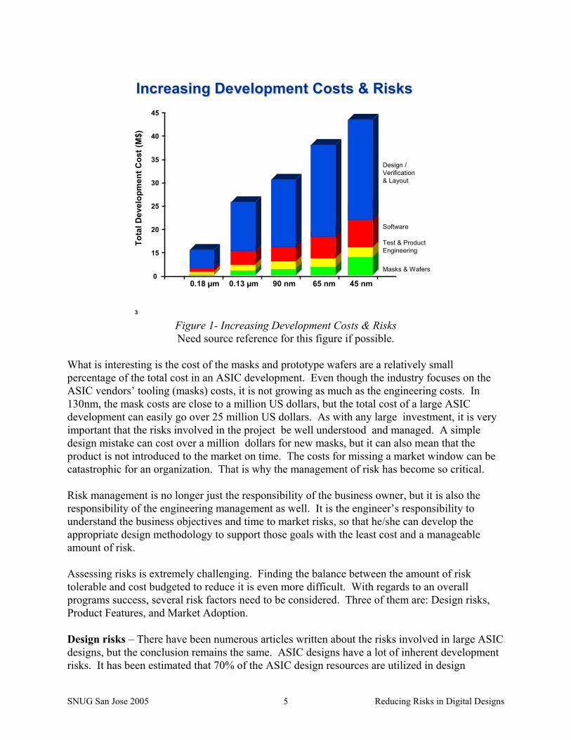
Figure 1- Increasing Development Costs & Risks Need source reference for this figure if possible.
What is interesting is the cost of the masks and prototype wafers are a relatively small percentage of the total cost in an ASIC development. Even though the industry focuses on the ASIC vendors’ tooling (masks) costs, it is not growing as much as the engineering costs. In 130nm, the mask costs are close to a million US dollars, but the total cost of a large ASIC development can easily go over 25 million US dollars. As with any large investment, it is very important that the risks involved in the project be well understood and managed. A simple design mistake can cost over a million dollars for new masks, but it can also mean that the product is not introduced to the market on time. The costs for missing a market window can be catastrophic for an organization. That is why the management of risk has become so critical. Risk management is no longer just the responsibility of the business owner, but it is also the responsibility of the engineering management as well. It is the engineer’s responsibility to understand the business objectives and time to market risks, so that he/she can develop the appropriate design methodology to support those goals with the least cost and a manageable amount of risk. Assessing risks is extremely challenging. Finding the balance between the amount of risk tolerable and cost budgeted to reduce it is even more difficult. With regards to an overall programs success, several risk factors need to be considered. Three of them are: Design risks, Product Features, and Market Adoption. Design risks – There have been numerous articles written about the risks involved in large ASIC designs, but the conclusion remains the same. ASIC designs have a lot of inherent development risks. It has been estimated that 70% of the ASIC design resources are utilized in design
SNUG San Jose 2005 Reducing Risks in Digital Designs 6
verification and not the actual RTL coding itself. If you include in-system verification, the design verification time and resources percentage is even higher. Even with all this emphasis on design verification, there are still numerous mistakes that occur for whatever reason. According to Dataquest, 70% of the ASIC designs require one full layer respin, so most prudent companies budget for at least one full layer respin when planning a project and when performing a return on investment (ROI) analysis. Product Features – Especially in the case of a new or emerging market, it is very difficult to predict which particular features will be critical for a products success. In many cases a field trial is required before feedback can be provided by potential customers. The oversight of leaving out a feature or critical functionality may sometimes be fixed using software or by adding an additional component in-system. In other cases, it will require a design respin that could delay the product launch for numerous months resulting in missing the early market window. Although the ensuing cost for the additional feature can be in the millions, the revenue and profit lost by not having the right product at the right time can spell disaster for the product. Market Adoption – It is very difficult to predict how and when a market will adopt new products and technologies. If possible, it would be ideal to defer as much costs without jeopardizing the ability to bring a product into market as quickly as possible. Having various production options is the key to maximizing productivity under unclear and sometimes blurry market conditions. Despite all the efforts of having the right product and the right execution, sometimes the market is not ready to embrace a new product or technology so delaying mass production may be the right business option. By delaying the mass production, the most cost effective process technology can be used to maximize the rate of return as well as thwart competitive cost pressure from competing products that are being manufactured in more advance process technologies. 2.2 Advantages of ASIC Prototyping with FPGAs As was just stated there are three areas of risk involved in the development of new products and technology, but they are not the only risks involved. In order to minimize these risks and others, many developers are turning to FPGAs and prototyping their ASICs. According to Dataquest, 41% of SoC designers are using FPGA prototypes for their ASIC designs. There are several reasons to adopt ASIC prototyping as part of a design methodology:
1. Comprehensive Verification – Even with the fastest available workstations, design simulation is inherently slow. In order to simulate a few seconds of a packet switch ASIC it may require one year of simulation run time. It is just improbable that a developer has that much time available to perform such simulation, so he/she must select the specific conditions that he/she wants to simulate. Unfortunately, it is very difficult to develop fully comprehensive test benches that can cover every single condition or situation that the device may experience in system. By using an FPGA for prototyping, an engineer can run the device in system to exercise it in a real world situation and identify any potential design flaw that may not have been detected during simulation.
2. Firmware development – Software development has become a larger part of the overall development cycle. Several years ago, many system companies revealed that their
SNUG San Jose 2005 Reducing Risks in Digital Designs 7
headcount for software developers have exceeded their headcount for hardware development. With the extended time and resources necessary for software development, having a prototype system available for software development can help shorten the overall development cycle. It can also uncover bugs, compatibility issues, and new hardware functions to support functionality that cannot be properly addressed or implemented by software. Minor tweaks and changes in hardware/software design and partitioning are simple and viable in a programmable device, but it is very costly to perform such tradeoffs and system investigation once the ASIC has been created.
3. Field Testing – Having systems that can be used for field testing can help uncover system or device flaws that were not discovered in the laboratory. New features and functionalities may also be required that was not in the original specification. FPGA prototype can be modified quickly to support any necessary modifications without large Non-Recurring Engineering fees or long manufacturing cycles. In many cases, having a demonstration system is a necessary requirement for the salesperson to secure a customer pre-order.
4. Production Options – As mentioned before, there are many market risks that are associated with the success of a product, especially for an emerging market. In the early part of a program, it is very difficult to forecast the number of units that will be required. Based upon the unit volume, the best return on investment may be production in an FPGA, a structured ASIC or a standard cell ASIC. Ideally, it would be advantageous to be able to prolong the decision as to which form of mass production makes sense for the product until the end of the design cycle versus the very beginning. By utilizing an FPGA for prototyping, the developer can focus on finalizing the design code and the business owner can observe the market conditions and then make a final decision as to how to proceed with production. This flexibility at the tail end of the design cycle can save the organization millions of dollars by avoiding costly mistakes as to which production option is best.
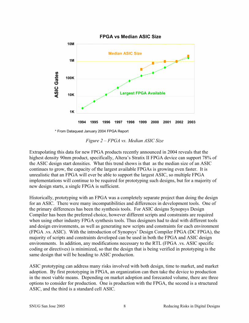
The adoption of using FPGAs for ASIC prototyping is gaining steady momentum, but there is still reluctance by some designers to adopt this methodology. In conversations with different development groups, the two largest complaints raised have been that FPGAs are not large enough to support their ASIC gate count, and that the design flow for an FPGA and ASIC is not compatible enough (ex. The design RTL was coded specifically for an FPGA). Over the course of the past year, advances in technology in both FPGA and design tools have addressed some of these concerns. More recently, technologies introduced by Synopsys have taken big strides in addressing these particular complaints. Historically the problem with prototyping ASIC designs using FPGAs was that the ASIC designs where just too large to fit in a single FPGA, so these designs had to be partitioned into multiple FPGA devices and system boards developed for the prototyping had to be redesigned for production once the multiple FPGAs were replaced by the ASIC. FPGA densities may now be less of an issue today. New industry data released in January 2004 from Dataquest has revealed that currently available FPGA device densities have basically caught up to the median density of ASIC designs. This means over 50% of the ASIC designs can now be prototyped in a single FPGA.
SNUG San Jose 2005 Reducing Risks in Digital Designs 8
ASI
C G
ates
ASI
C G
ates
1K
1994 1995 1996 1997 1998 1999 2000 2001 2002 2003
10K
100K
1M
10M
Largest FPGA Available
Median ASIC Size
* From Dataquest January 2004 FPGA Report
FPGA vs Median ASIC Size
Figure 2 – FPGA vs. Median ASIC Size
Extrapolating this data for new FPGA products recently announced in 2004 reveals that the highest density 90nm product, specifically, Altera’s Stratix II FPGA device can support 78% of the ASIC design start densities. What this trend shows is that as the median size of an ASIC continues to grow, the capacity of the largest available FPGAs is growing even faster. It is unrealistic that an FPGA will ever be able to support the largest ASIC, so multiple FPGA implementations will continue to be required for prototyping such designs, but for a majority of new design starts, a single FPGA is sufficient. Historically, prototyping with an FPGA was a completely separate project than doing the design for an ASIC. There were many incompatibilities and differences in development tools. One of the primary differences has been the synthesis tools. For ASIC designs Synopsys Design Compiler has been the preferred choice, however different scripts and constraints are required when using other industry FPGA synthesis tools. Thus designers had to deal with different tools and design environments, as well as generating new scripts and constraints for each environment (FPGA .vs. ASIC). With the introduction of Synopsys’ Design Compiler FPGA (DC FPGA), the majority of scripts and constraints developed can be used in both the FPGA and ASIC design environments. In addition, any modifications necessary to the RTL (FPGA .vs. ASIC specific coding or directives) is minimized, so that the design that is being verified in prototyping is the same design that will be heading to ASIC production. ASIC prototyping can address many risks involved with both design, time to market, and market adoption. By first prototyping in FPGA, an organization can then take the device to production in the most viable means. Depending on market adoption and forecasted volume, there are three options to consider for production. One is production with the FPGA, the second is a structured ASIC, and the third is a standard cell ASIC.
SNUG San Jose 2005 Reducing Risks in Digital Designs 9
Unified Unified FlowFlow
Standard Cell ASIC
High Volume
Time
FPGA
Low to Medium Volume
Time
DC/DC FPGA
DC/DC FPGA
HardCopy
Medium to High Volume
Time
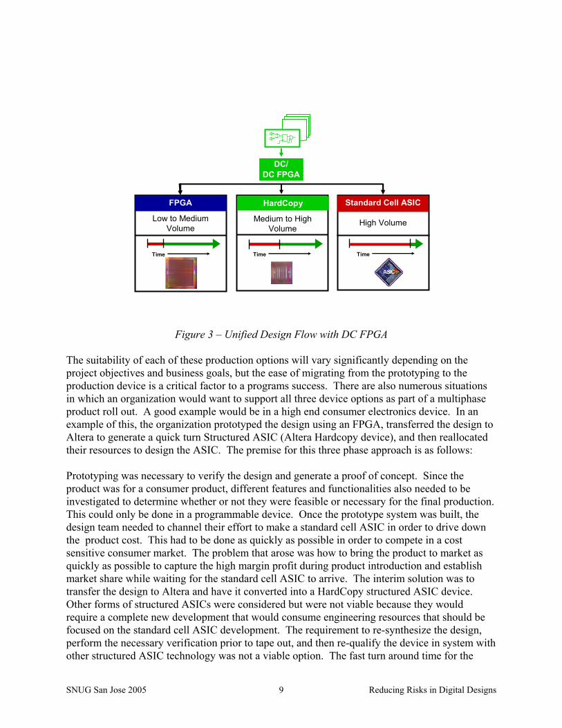
Figure 3 – Unified Design Flow with DC FPGA
The suitability of each of these production options will vary significantly depending on the project objectives and business goals, but the ease of migrating from the prototyping to the production device is a critical factor to a programs success. There are also numerous situations in which an organization would want to support all three device options as part of a multiphase product roll out. A good example would be in a high end consumer electronics device. In an example of this, the organization prototyped the design using an FPGA, transferred the design to Altera to generate a quick turn Structured ASIC (Altera Hardcopy device), and then reallocated their resources to design the ASIC. The premise for this three phase approach is as follows: Prototyping was necessary to verify the design and generate a proof of concept. Since the product was for a consumer product, different features and functionalities also needed to be investigated to determine whether or not they were feasible or necessary for the final production. This could only be done in a programmable device. Once the prototype system was built, the design team needed to channel their effort to make a standard cell ASIC in order to drive down the product cost. This had to be done as quickly as possible in order to compete in a cost sensitive consumer market. The problem that arose was how to bring the product to market as quickly as possible to capture the high margin profit during product introduction and establish market share while waiting for the standard cell ASIC to arrive. The interim solution was to transfer the design to Altera and have it converted into a HardCopy structured ASIC device. Other forms of structured ASICs were considered but were not viable because they would require a complete new development that would consume engineering resources that should be focused on the standard cell ASIC development. The requirement to re-synthesize the design, perform the necessary verification prior to tape out, and then re-qualify the device in system with other structured ASIC technology was not a viable option. The fast turn around time for the
SNUG San Jose 2005 Reducing Risks in Digital Designs 10
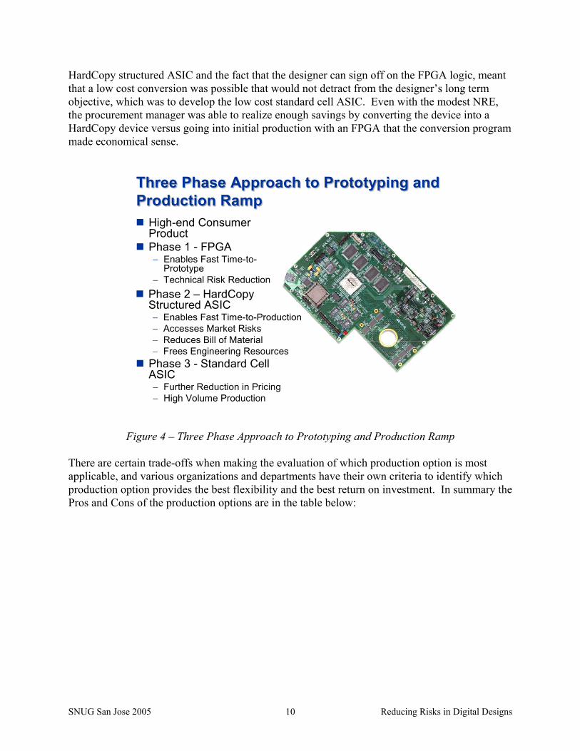
HardCopy structured ASIC and the fact that the designer can sign off on the FPGA logic, meant that a low cost conversion was possible that would not detract from the designer’s long term objective, which was to develop the low cost standard cell ASIC. Even with the modest NRE, the procurement manager was able to realize enough savings by converting the device into a HardCopy device versus going into initial production with an FPGA that the conversion program made economical sense.
Phase 2 – HardCopy Structured ASIC− Enables Fast Time-to-Production− Accesses Market Risks− Reduces Bill of Material− Frees Engineering Resources
Phase 3 - Standard Cell ASIC− Further Reduction in Pricing− High Volume Production
Three Phase Approach to Prototyping and Production RampThree Phase Approach to Prototyping and Production Ramp
High-end Consumer ProductPhase 1 - FPGA− Enables Fast Time-to-
Prototype− Technical Risk Reduction
Figure 4 – Three Phase Approach to Prototyping and Production Ramp
There are certain trade-offs when making the evaluation of which production option is most applicable, and various organizations and departments have their own criteria to identify which production option provides the best flexibility and the best return on investment. In summary the Pros and Cons of the production options are in the table below:
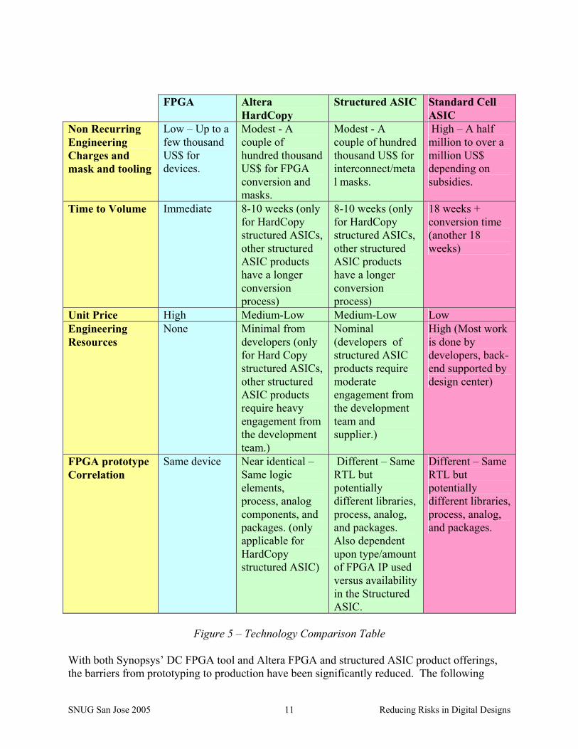
SNUG San Jose 2005 Reducing Risks in Digital Designs 11
FPGA Altera
HardCopy Structured ASIC Standard Cell
ASIC Non Recurring Engineering Charges and mask and tooling
Low – Up to a few thousand US$ for devices.
Modest - A couple of hundred thousand US$ for FPGA conversion and masks.
Modest - A couple of hundred thousand US$ for interconnect/metal masks.
High – A half million to over a million US$ depending on subsidies.
Time to Volume Immediate 8-10 weeks (only for HardCopy structured ASICs, other structured ASIC products have a longer conversion process)
8-10 weeks (only for HardCopy structured ASICs, other structured ASIC products have a longer conversion process)
18 weeks + conversion time (another 18 weeks)
Unit Price High Medium-Low Medium-Low Low Engineering Resources
None Minimal from developers (only for Hard Copy structured ASICs, other structured ASIC products require heavy engagement from the development team.)
Nominal (developers of structured ASIC products require moderate engagement from the development team and supplier.)
High (Most work is done by developers, back-end supported by design center)
FPGA prototype Correlation
Same device Near identical – Same logic elements, process, analog components, and packages. (only applicable for HardCopy structured ASIC)
Different – Same RTL but potentially different libraries, process, analog, and packages. Also dependent upon type/amount of FPGA IP used versus availability in the Structured ASIC.
Different – Same RTL but potentially different libraries, process, analog, and packages.
Figure 5 – Technology Comparison Table
With both Synopsys’ DC FPGA tool and Altera FPGA and structured ASIC product offerings, the barriers from prototyping to production have been significantly reduced. The following

SNUG San Jose 2005 Reducing Risks in Digital Designs 12
sections provides some background information on the complementary technologies and demonstrate the process of a prototyping with and Altera FPGA and then migrating that design into a HardCopy device.
SNUG San Jose 2005 Reducing Risks in Digital Designs 13
3.0 Background on Synopsys’ DC FPGA Synthesis Tool and Altera’s HardCopy Structured ASIC
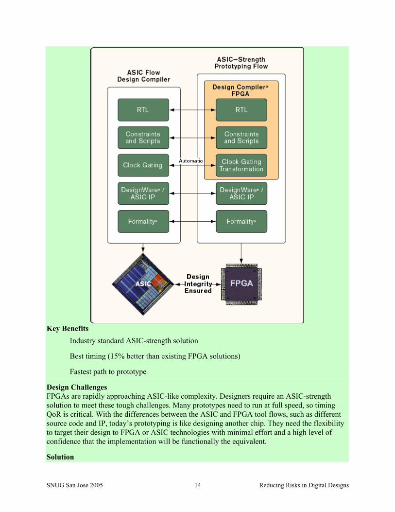
3.1 Synopsys’ DC FPGA Synopsys had done a fairly thorough job of describing the DC FPGA product, so I will just extract the information from their website. Below is an extract of DC FPGA from Synopsys’ website: Design Compiler FPGA The Best FPGA Synthesis for ASIC Prototyping--Design Once! Overview Design Compiler FPGA is the only solution available today that is targeted specifically for designers who prototype ASICs using high-end FPGAs. These are the designs that require an ASIC-strength solution. Built upon Synopsys’ Design Compiler technology and incorporating new Adaptive Optimization™ technology, DC FPGA provides the most advanced ASIC synthesis technologies for FPGAs—resulting in a best timing QoR and reliable design results. By eliminating the time consuming and error prone manual conversion between ASIC and FPGA designs, Design Compiler FPGA allows designers to design once at the RTL level and easily target the design to an FPGA prototype and ASIC implementation.
SNUG San Jose 2005 Reducing Risks in Digital Designs 14
Key Benefits
Industry standard ASIC-strength solution
Best timing (15% better than existing FPGA solutions)
Fastest path to prototype
Design Challenges FPGAs are rapidly approaching ASIC-like complexity. Designers require an ASIC-strength solution to meet these tough challenges. Many prototypes need to run at full speed, so timing QoR is critical. With the differences between the ASIC and FPGA tool flows, such as different source code and IP, today’s prototyping is like designing another chip. They need the flexibility to target their design to FPGA or ASIC technologies with minimal effort and a high level of confidence that the implementation will be functionally the equivalent.
Solution
SNUG San Jose 2005 Reducing Risks in Digital Designs 15
DC FPGA combines the leading ASIC synthesis technology of Design Compiler with new revolutionary Adaptive Optimization (AO) technology delivering the ideal solution for prototyping even the most complex ASIC designs onto high-end FPGAs.
DC FPGA is compatible with the Galaxy Design and Discovery Verification platforms providing designer access to an ASIC-strength solution to handle their high-end FPGAs. Add to that, AO technology and you get the best timing—15% better timing on average than traditional FPGA synthesis tools. By using a common, robust ASIC and FPGA flow, designers can design once for both their ASIC and FPGA and get the fastest path to prototype and integrity is ensured.
DC FPGA enables you to Design Once.
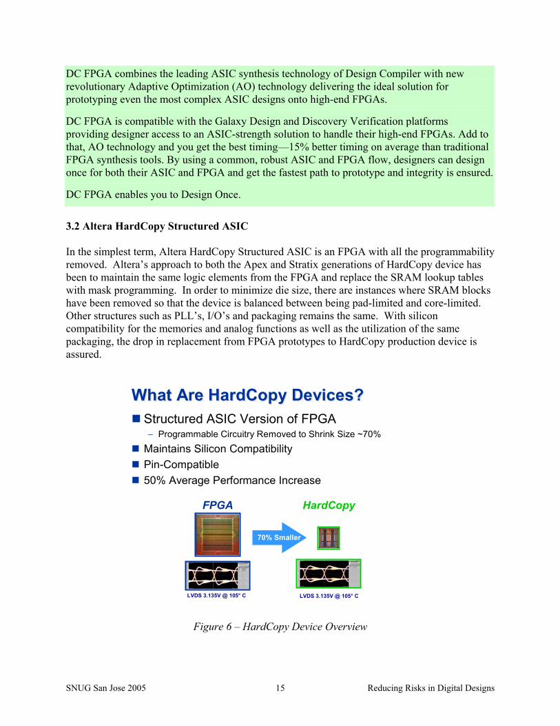
3.2 Altera HardCopy Structured ASIC In the simplest term, Altera HardCopy Structured ASIC is an FPGA with all the programmability removed. Altera’s approach to both the Apex and Stratix generations of HardCopy device has been to maintain the same logic elements from the FPGA and replace the SRAM lookup tables with mask programming. In order to minimize die size, there are instances where SRAM blocks have been removed so that the device is balanced between being pad-limited and core-limited. Other structures such as PLL’s, I/O’s and packaging remains the same. With silicon compatibility for the memories and analog functions as well as the utilization of the same packaging, the drop in replacement from FPGA prototypes to HardCopy production device is assured.
What Are HardCopy Devices?What Are HardCopy Devices?Structured ASIC Version of FPGA− Programmable Circuitry Removed to Shrink Size ~70%
Maintains Silicon CompatibilityPin-Compatible50% Average Performance Increase
LVDS 3.135V @ 105° C
70% Smaller
FPGA HardCopy
LVDS 3.135V @ 105° C
Figure 6 – HardCopy Device Overview
SNUG San Jose 2005 Reducing Risks in Digital Designs 16
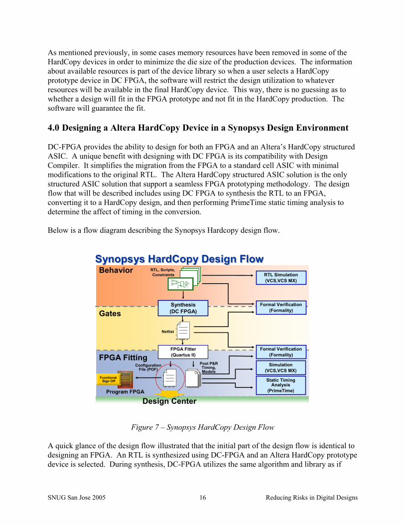
As mentioned previously, in some cases memory resources have been removed in some of the HardCopy devices in order to minimize the die size of the production devices. The information about available resources is part of the device library so when a user selects a HardCopy prototype device in DC FPGA, the software will restrict the design utilization to whatever resources will be available in the final HardCopy device. This way, there is no guessing as to whether a design will fit in the FPGA prototype and not fit in the HardCopy production. The software will guarantee the fit. 4.0 Designing a Altera HardCopy Device in a Synopsys Design Environment DC-FPGA provides the ability to design for both an FPGA and an Altera’s HardCopy structured ASIC. A unique benefit with designing with DC FPGA is its compatibility with Design Compiler. It simplifies the migration from the FPGA to a standard cell ASIC with minimal modifications to the original RTL. The Altera HardCopy structured ASIC solution is the only structured ASIC solution that support a seamless FPGA prototyping methodology. The design flow that will be described includes using DC FPGA to synthesis the RTL to an FPGA, converting it to a HardCopy design, and then performing PrimeTime static timing analysis to determine the affect of timing in the conversion. Below is a flow diagram describing the Synopsys Hardcopy design flow.
Behavior
Gates
FPGA Fitting
Synopsys HardCopy Design FlowSynopsys HardCopy Design FlowRTL, Scripts, Constraints
Netlist
ConfigurationFile (POF)
Post P&RTiming,Models
Synthesis(DC FPGA)
RTL Simulation(VCS,VCS MX)
Formal Verification(Formality)
Simulation(VCS,VCS MX)
Static Timing Analysis
(PrimeTime)
FPGA Fitter(Quartus II)
Formal Verification(Formality)
Design CenterProgram FPGA
Functional Sign Off
Functional Sign Off
Figure 7 – Synopsys HardCopy Design Flow
A quick glance of the design flow illustrated that the initial part of the design flow is identical to designing an FPGA. An RTL is synthesized using DC-FPGA and an Altera HardCopy prototype device is selected. During synthesis, DC-FPGA utilizes the same algorithm and library as if
SNUG San Jose 2005 Reducing Risks in Digital Designs 17
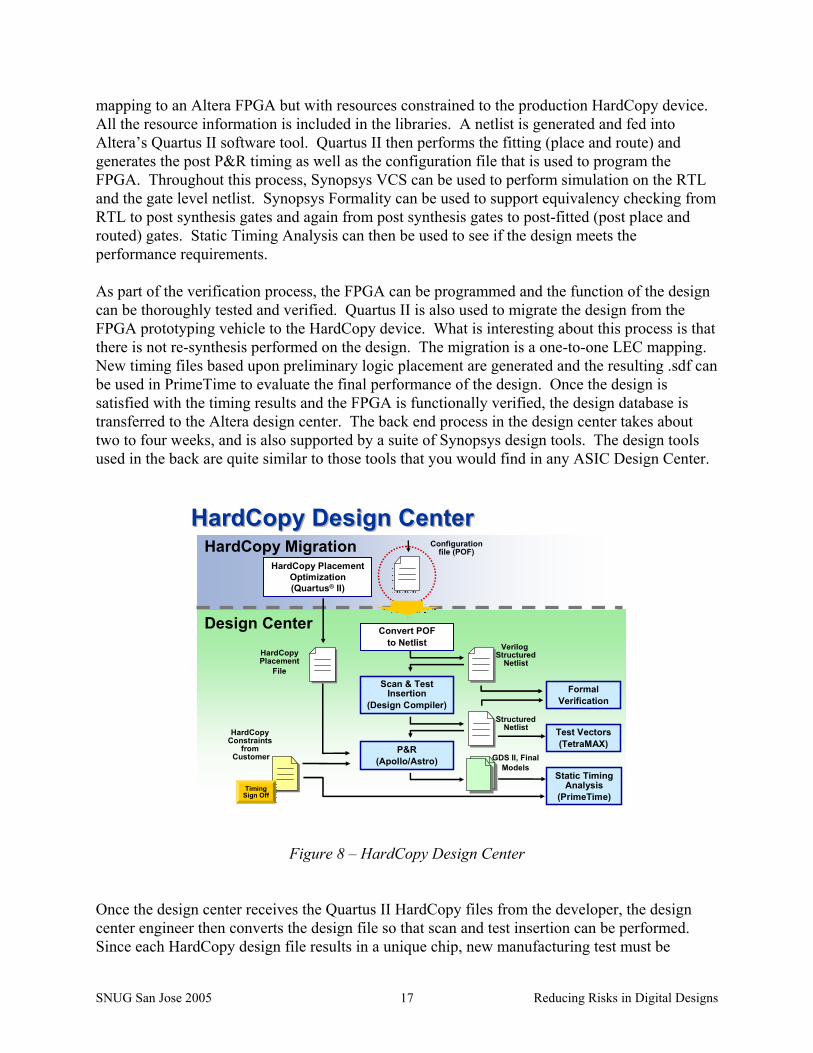
mapping to an Altera FPGA but with resources constrained to the production HardCopy device. All the resource information is included in the libraries. A netlist is generated and fed into Altera’s Quartus II software tool. Quartus II then performs the fitting (place and route) and generates the post P&R timing as well as the configuration file that is used to program the FPGA. Throughout this process, Synopsys VCS can be used to perform simulation on the RTL and the gate level netlist. Synopsys Formality can be used to support equivalency checking from RTL to post synthesis gates and again from post synthesis gates to post-fitted (post place and routed) gates. Static Timing Analysis can then be used to see if the design meets the performance requirements. As part of the verification process, the FPGA can be programmed and the function of the design can be thoroughly tested and verified. Quartus II is also used to migrate the design from the FPGA prototyping vehicle to the HardCopy device. What is interesting about this process is that there is not re-synthesis performed on the design. The migration is a one-to-one LEC mapping. New timing files based upon preliminary logic placement are generated and the resulting .sdf can be used in PrimeTime to evaluate the final performance of the design. Once the design is satisfied with the timing results and the FPGA is functionally verified, the design database is transferred to the Altera design center. The back end process in the design center takes about two to four weeks, and is also supported by a suite of Synopsys design tools. The design tools used in the back are quite similar to those tools that you would find in any ASIC Design Center.
HardCopy Design CenterHardCopy Design Center
StructuredNetlistHardCopy
Constraints from
Customer
Configurationfile (POF)
Design Center
FormalVerification
P&R(Apollo/Astro)
Convert POFto Netlist
Scan & Test Insertion
(Design Compiler)
Verilog Structured
Netlist
GDS II, FinalModels
HardCopy Placement Optimization (Quartus® II)
HardCopyPlacement
File
HardCopy Migration
Static Timing Analysis
(PrimeTime)
Test Vectors(TetraMAX)
TimingSign OffTiming
Sign Off
Figure 8 – HardCopy Design Center
Once the design center receives the Quartus II HardCopy files from the developer, the design center engineer then converts the design file so that scan and test insertion can be performed. Since each HardCopy design file results in a unique chip, new manufacturing test must be
SNUG San Jose 2005 Reducing Risks in Digital Designs 18
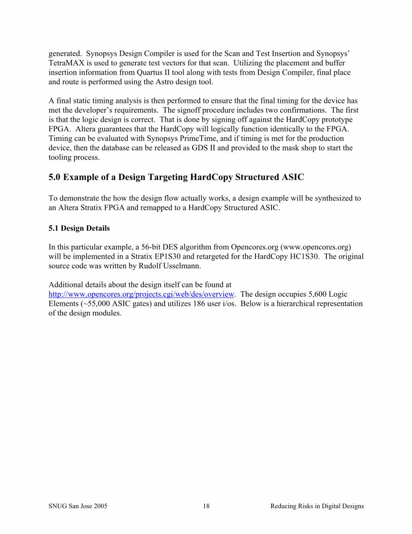
generated. Synopsys Design Compiler is used for the Scan and Test Insertion and Synopsys’ TetraMAX is used to generate test vectors for that scan. Utilizing the placement and buffer insertion information from Quartus II tool along with tests from Design Compiler, final place and route is performed using the Astro design tool. A final static timing analysis is then performed to ensure that the final timing for the device has met the developer’s requirements. The signoff procedure includes two confirmations. The first is that the logic design is correct. That is done by signing off against the HardCopy prototype FPGA. Altera guarantees that the HardCopy will logically function identically to the FPGA. Timing can be evaluated with Synopsys PrimeTime, and if timing is met for the production device, then the database can be released as GDS II and provided to the mask shop to start the tooling process. 5.0 Example of a Design Targeting HardCopy Structured ASIC To demonstrate the how the design flow actually works, a design example will be synthesized to an Altera Stratix FPGA and remapped to a HardCopy Structured ASIC. 5.1 Design Details In this particular example, a 56-bit DES algorithm from Opencores.org (www.opencores.org) will be implemented in a Stratix EP1S30 and retargeted for the HardCopy HC1S30. The original source code was written by Rudolf Usselmann. Additional details about the design itself can be found at http://www.opencores.org/projects.cgi/web/des/overview. The design occupies 5,600 Logic Elements (~55,000 ASIC gates) and utilizes 186 user i/os. Below is a hierarchical representation of the design modules.
SNUG San Jose 2005 Reducing Risks in Digital Designs 19
KEY_SEL.V
DES.V
CRP.V
SBOX1.V
SBOX2.V
SBOX3.V
SBOX4.V
SBOX5.V
SBOX6.V
SBOX7.V
SBOX8.V
Original Source Code Written by Rudolf Usselmann
Figure 9 – Block Diagram of 56 bit DES Example Design
5.2 Synthesizing with DC FPGA The following script was used for DC FPGA: set dcfpga_lib_path " /home/jtai/software/dc/libraries/2004.03" set design des_top set outputdir dcfpga_work #file delete -force $outputdir define_design_lib WORK -path $outputdir set search_path ". $search_path $dcfpga_lib_path/STRATIX /home/jtai/projects/snug_sj2004/rtl" set target_library "stratix.db" set synthetic_library "tmg.sldb altera_mf.sldb LPM.sldb" set link_library "* stratix.db tmg.sldb altera_mf.sldb LPM.sldb" define_design_lib altera_mf -path $dcfpga_lib_path/STRATIX/altera_mf_lib define_design_lib LPM -path $dcfpga_lib_path/STRATIX/LPM set edifout_netlist_only "true" set edifout_power_and_ground_representation "net" set edifout_ground_net_name "GND" set edifout_power_net_name "VDD" set hdlin_enable_vpp "true" set edifout_write_properties_list "lut_function part IOSTANDARD DRIVE SLEW" set post_compile_cost_check "false" set_fpga_defaults altera_stratix
SNUG San Jose 2005 Reducing Risks in Digital Designs 20
analyze -format verilog { des_top.v pll_bb.v crp.v key_sel.v sbox1.v sbox2.v sbox3.v sbox4.v sbox5.v sbox6.v sbox7.v sbox8.v } elaborate $design current_design $design set_dont_touch [get_cell u_pll] true link set_fpga_target_device EP1S30F780C5_HARDCOPY_FPGA_PROTOTYPE create_clock -period 5.5 [get_ports clk] set_propagated_clocks set_input_delay -max 4 -clock clk [remove_from_collection [all_inputs] [get_ports clk]] set_output_delay -max 4 -clock clk [get_ports desOut] check_timing ungroup -small 500 compile write -f edif -hier -o $outputdir/$design.edf write_par_constraint $outputdir/$design.tcl 5.3 Setting up Quartus II Project The following script was used to set up Quartus II Project # Project-Wide Assignments # ======================== set_global_assignment -name ORIGINAL_QUARTUS_VERSION 4.0 set_global_assignment -name PROJECT_CREATION_TIME_DATE "14:40:19 MARCH 15, 2004" set_global_assignment -name LAST_QUARTUS_VERSION 4.0 set_global_assignment -name VERILOG_FILE ../pll.v # Timing Assignments # ================== set_global_assignment -name TSU_REQUIREMENT 4ns set_global_assignment -name TCO_REQUIREMENT 4ns set_global_assignment -name INCLUDE_EXTERNAL_PIN_DELAYS_IN_FMAX_CALCULATIONS OFF # Analysis & Synthesis Assignments # ================================ set_global_assignment -name FAMILY Stratix set_global_assignment -name EDA_DESIGN_ENTRY_SYNTHESIS_TOOL "Design Compiler" set_global_assignment -name TOP_LEVEL_ENTITY des_top # Fitter Assignments # ================== set_global_assignment -name DEVICE EP1S30F780C5_HARDCOPY_FPGA_PROTOTYPE # EDA Netlist Writer Assignments # ============================== set_global_assignment -name EDA_TIMING_ANALYSIS_TOOL "PrimeTime (Verilog HDL output from Quartus II)" # Design Assistant Assignments # ============================ set_global_assignment -name HARDCOPY_FLOW_AUTOMATION COMPILE_NEW_PROJECT set_global_assignment -name HARDCOPY_NEW_PROJECT_PATH ../hardcopy_work/
SNUG San Jose 2005 Reducing Risks in Digital Designs 21
# ---------------- # start CLOCK(clk) # Timing Assignments # ================== set_global_assignment -name FMAX_REQUIREMENT "5.0 ns" -section_id clk set_global_assignment -name DUTY_CYCLE 50 -section_id clk set_global_assignment -name DIVIDE_BASE_CLOCK_PERIOD_BY 1 -section_id clk set_global_assignment -name MULTIPLY_BASE_CLOCK_PERIOD_BY 1 -section_id clk set_global_assignment -name INVERT_BASE_CLOCK OFF -section_id clk set_global_assignment -name INCLUDE_EXTERNAL_PIN_DELAYS_IN_FMAX_CALCULATIONS OFF -section_id clk # end CLOCK(clk) # -------------- # --------------------------------------------- # start EDA_TOOL_SETTINGS(eda_design_synthesis) # Analysis & Synthesis Assignments # ================================ set_global_assignment -name EDA_INPUT_VCC_NAME VDD -section_id eda_design_synthesis set_global_assignment -name EDA_LMF_FILE altsyn.lmf -section_id eda_design_synthesis # end EDA_TOOL_SETTINGS(eda_design_synthesis) # ------------------------------------------- # -------------------------------------------- # start EDA_TOOL_SETTINGS(eda_timing_analysis) # EDA Netlist Writer Assignments # ============================== set_global_assignment -name EDA_TIME_SCALE "1 ps" -section_id eda_timing_analysis set_global_assignment -name EDA_OUTPUT_DATA_FORMAT VERILOG -section_id eda_timing_analysis # end EDA_TOOL_SETTINGS(eda_timing_analysis) # ------------------------------------------ # --------------------- # start ENTITY(des_top) # Timing Assignments # ================== set_instance_assignment -name CLOCK_SETTINGS clk -to clk set_instance_assignment -name INPUT_MAX_DELAY 4.0 -from clk -to "desIn\[63\] desIn\[62\] desIn\[61\] desIn\[60\] desIn\[59\] desIn\[58\] desIn\[57\] desIn\[56\] desIn\[55\] desIn\[54\] desIn\[53\] desIn\[52\] desIn\[51\] desIn\[50\] desIn\[49\] desIn\[48\] desIn\[47\] desIn\[46\] desIn\[45\] desIn\[44\] desIn\[43\] desIn\[42\] desIn\[41\] desIn\[40\] desIn\[39\] desIn\[38\] desIn\[37\] desIn\[36\] desIn\[35\] desIn\[34\] desIn\[33\] desIn\[32\] desIn\[31\] desIn\[30\] desIn\[29\] desIn\[28\] desIn\[27\] desIn\[26\] desIn\[25\] desIn\[24\] desIn\[23\] desIn\[22\] desIn\[21\] desIn\[20\] desIn\[19\] desIn\[18\] desIn\[17\] desIn\[16\] desIn\[15\] desIn\[14\] desIn\[13\] desIn\[12\] desIn\[11\] desIn\[10\]
SNUG San Jose 2005 Reducing Risks in Digital Designs 22
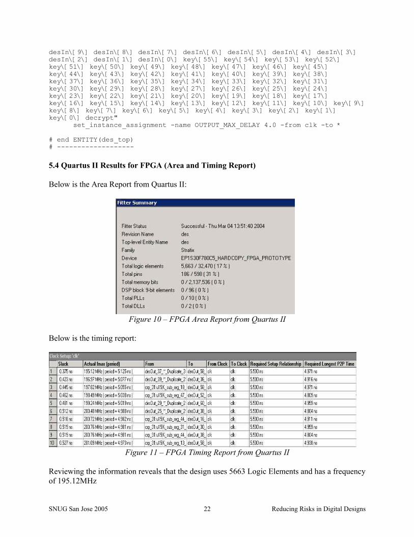
desIn\[9\] desIn\[8\] desIn\[7\] desIn\[6\] desIn\[5\] desIn\[4\] desIn\[3\] desIn\[2\] desIn\[1\] desIn\[0\] key\[55\] key\[54\] key\[53\] key\[52\] key\[51\] key\[50\] key\[49\] key\[48\] key\[47\] key\[46\] key\[45\] key\[44\] key\[43\] key\[42\] key\[41\] key\[40\] key\[39\] key\[38\] key\[37\] key\[36\] key\[35\] key\[34\] key\[33\] key\[32\] key\[31\] key\[30\] key\[29\] key\[28\] key\[27\] key\[26\] key\[25\] key\[24\] key\[23\] key\[22\] key\[21\] key\[20\] key\[19\] key\[18\] key\[17\] key\[16\] key\[15\] key\[14\] key\[13\] key\[12\] key\[11\] key\[10\] key\[9\] key\[8\] key\[7\] key\[6\] key\[5\] key\[4\] key\[3\] key\[2\] key\[1\] key\[0\] decrypt" set_instance_assignment -name OUTPUT_MAX_DELAY 4.0 -from clk -to * # end ENTITY(des_top) # ------------------- 5.4 Quartus II Results for FPGA (Area and Timing Report) Below is the Area Report from Quartus II:
Figure 10 – FPGA Area Report from Quartus II
Below is the timing report:
Figure 11 – FPGA Timing Report from Quartus II
Reviewing the information reveals that the design uses 5663 Logic Elements and has a frequency of 195.12MHz
SNUG San Jose 2005 Reducing Risks in Digital Designs 23
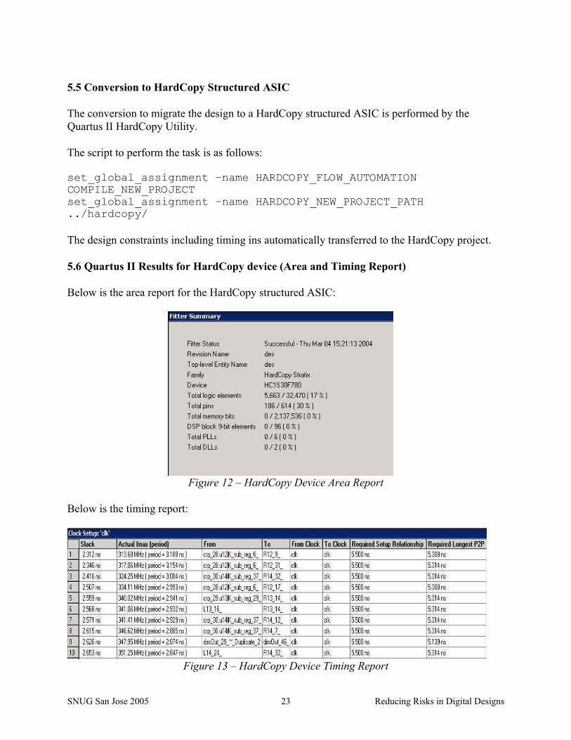
5.5 Conversion to HardCopy Structured ASIC The conversion to migrate the design to a HardCopy structured ASIC is performed by the Quartus II HardCopy Utility. The script to perform the task is as follows: set_global_assignment –name HARDCOPY_FLOW_AUTOMATION COMPILE_NEW_PROJECT set_global_assignment –name HARDCOPY_NEW_PROJECT_PATH ../hardcopy/ The design constraints including timing ins automatically transferred to the HardCopy project. 5.6 Quartus II Results for HardCopy device (Area and Timing Report) Below is the area report for the HardCopy structured ASIC:
Figure 12 – HardCopy Device Area Report
Below is the timing report:
Figure 13 – HardCopy Device Timing Report
SNUG San Jose 2005 Reducing Risks in Digital Designs 24
Reviewing the report files reveal that the design occupies 5663 logic elements and has a frequencies of 313.68MHz. 6.0 PrimeTime Static Timing Analysis on the FPGA and HardCopy Structured ASIC 6.1 PrimeTime Scripts Both Altera and Synopsys have worked cooperatively and Quartus II can generate the scripts necessary to run PrimeTime. Below is an example of the script used for this particular design analysis: read_verilog -hdl_compiler des.vo current_design des link read_sdf des_v.sdo create_clock -period 5.500 -waveform {0 2.750} [get_ports clk ] -name clk set_propagated_clock [all_clocks] set_input_delay -max -add_delay 1.500 -clock [get_clocks clk ] [get_ports decrypt ] set_input_delay -max -add_delay 1.500 -clock [get_clocks clk ] [get_ports desIn ] set_input_delay -max -add_delay 1.500 -clock [get_clocks clk ] [get_ports key ] set_output_delay -max -add_delay 1.500 -clock [get_clocks clk ] [get_ports desOut ] 6.2 PrimeTime Static Timing Report for the FPGA Below is the timing report that was generated by PrimeTime for the FPGA: Startpoint: desOut_reg_37~0.lereg (rising edge-triggered flip-flop clocked by clk) Endpoint: desOut[58]~I.out_reg (rising edge-triggered flip-flop clock by clk) Path Group: clk Path Type: max Point Incr Path -------------------------------------------------------------------------- clock clk (rise edge) 0.000 0.000 clock network delay (propagated) 2.822 2.822 desOut_reg_37~0.lereg.clk (stratic_lcell_register) 0.000 2.822 r desOut_reg_37~0.lereg.regout (stratix_lcell_register) 0.579 3.401 r u15.n326~39_I.datad (stratix_asynch_lcell) 1.031 4.432 r … desOut[58]~I.outreg.datain (stratix_io_register) 0.278 8.090 r data arrival time 8.090 r clock clk (rise edge) 5.500 5.500 clock network delay (propagated) 3.119 8.619 desOut[58]~I.out_reg.clk (stratix_io_register) 8.619 r
SNUG San Jose 2005 Reducing Risks in Digital Designs 25
library setup time -0.076 8.543 data required time 8.543 -------------------------------------------------------------------------- data required time 8.090 data arrival time 7.715 -------------------------------------------------------------------------- slack (MET) 0.375 6.3 PrimeTime Static Timing Report for the HardCopy Structured ASIC Below is the timing report that was generated by PrimeTime for the HardCopy Structured ASIC: Startpoint: u12_aK_sub_reg_6_ (rising edge-triggered flip-flop clocked by clk) Endpoint: R12_reg_9__a0.regout (rising edge-triggered flip-flop clocked by clk) Path Group: clk Path Type: max Point Incr Path -------------------------------------------------------------------------- clock clk (rise edge) 0.000 0.000 clock network delay (propagated) 3.509 3.509 u12_aK_sub_reg6.lereg.clk (stratic_lcell_register) 0.000 3.509 r u12_aK_sub_reg6.lereg.regout (stratix_lcell_register) 0.280 3.789 r L12_reg_5__a0.datad (stratix_asynch_lcell) 0.843 4.634 r … R12_reg_9__a0.lecomb.regin (stratix_lcell_register) 0.364 6.698 r R12_reg_9__a0.lereg.datain (stratix_lcell_register) 0.000 6.698 r data arrival time 6.698 r clock clk (rise edge) 5.500 5.500 clock network delay (propagated) 3.515 9.015 R12_reg_9__a0.lereg.datain (stratix_lcell_register) 0.000 9.015 r library setup time -0.010 9.010 data required time 9.010 -------------------------------------------------------------------------- data required time 9.010 data arrival time 6.698 -------------------------------------------------------------------------- slack (MET) 2.312 6.4 Comparison of Timing Results Comparison of the timing results for the Stratix FPGA and the associated HardCopy structured ASIC shows that the HardCopy structured ASIC can benefit significantly in performance. Much this performance can be attributed to timing delays due to the interconnect. Even though the FPGA and the HardCopy device utilize the same logic element, the constricting of the physical design (by removing the programmability) shrinks the over die of the device and thus reducing the interconnect delays. This demonstrates the improvement of the HardCopy structured ASIC is not just lower cost because of smaller die, but also higher performance. Summary of results: Stratix FPGA – 195.12 MHz Stratix HardCopy structured ASIC – 313.68 MHz
SNUG San Jose 2005 Reducing Risks in Digital Designs 26
Performance gain of 61% As another comparison point, the same core was synthesized by Rudolf Usselmann in the following technologies for performance: 0.18um UMC ASIC process – 300MHz Xilinx Virtex-II-1500-6 – 166MHz Note that the HardCopy structured ASIC device compares favorably even against a standard cell ASIC implementation. 7.0 Conclusions and Recommendations Advanced process technologies offer as many risks as rewards. Managing those risks from both a technical and business perspective may require a change in how an organization implements its design and bring it into production. More and more designers are starting to prototype their designs in FPGA. Latest figures show that over 40% of ASIC designs are being prototyped. Despite the high percentage of designers prototyping, there still has been reluctance by some people to do so for two primary reasons. The first is that the FPGAs are not large enough to support the ASIC design. With advance products from Altera, it can be extrapolated that 78% of the ASIC designs can now fit on a single FPGA. Differences in the design environment was the second issue that many designers raised when confronted with the question of whether or not they wanted to do an FPGA prototype. With DC FPGA from Synopsys, the design environment for both FPGA and ASIC can be reused. For most instances, the same RTL, constraints and scripts can be used by both tools. Migrating from prototyping to production is now a more simplified process. With three production options – FPGA for low volume, HardCopy structured ASIC for medium volume, and standard cell ASIC for high volume, the program manager can select which production path is most suitable for the current market conditions. Seamless migration from FPGA to HardCopy Structured ASIC addresses low to medium production volumes. Reuse of the RTL, scripts and constraints when migrating from FPGA to a standard cell ASIC is addressed by DC FPGA. These new technologies from Altera and Synopys provide designers a clear path for prototyping, and the flexibility for program managers to decide the most appropriate production option. 8.0 Acknowledgements Richard Shaw, Staff CAE, Synopsys Jan-Sian Tai, Member of the Technical Staff, Altera 9.0 References Design Compiler FPGA presentation by Greg Tanaka, Synopsys User Wants and Needs 2003 by Gary Smith Gartner/Dataquest

101 Innovation DriveSan Jose, CA 95134(408) 544-7000www.altera.comApplications Hotline:(800) 800-EPLDLiterature Services:[email protected]
Copyright © 2005 Altera Corporation. All rights reserved. Altera, The Programmable Solutions Company, the stylized Altera logo, specificdevice designations, and all other words and logos that are identified as trademarks and/or service marks are, unless noted otherwise, thetrademarks and service marks of Altera Corporation in the U.S. and other countries. All other product or service names are the property oftheir respective holders. Altera products are protected under numerous U.S. and foreign patents and pending applications, maskwork rights,and copyrights. Altera warrants performance of its semiconductor products to current specifications in accordance with Altera's standardwarranty, but reserves the right to make changes to any products and services at any time without notice. Altera assumes no responsibility orliability arising out of the application or use of any information, product, or service described herein except as expressly agreed to in writingby Altera Corporation. Altera customers are advised to obtain the latest version of device specifications before relying on any published infor-mation and before placing orders for products or services.
All copyrights reserved.


![Metallic Electromigration Phenomena - Digchipapplication-notes.digchip.com/166/166-47937.pdfgrowth. (From [8].) When a filament finally bridges the gap between conductors, a sudden](https://img.pdfslide.us/doc/110x75/5ea91ad7bf50921a6b222985/metallic-electromigration-phenomena-digchipapplication-notes-growth-from-8.jpg)