Embed Size (px)
Citation preview

For Technology in Quality
User's Manual
STK-MB5329
STK MB5329 UM 100
18.03.2010

User's Manual STK MB5329 UM 100
Page 2
©2010 by TQ
-Com
ponents Gm
bH
Table of contents
1. ABOUT THIS MANUAL .......................................................................................................................... 7 1.1 TIPS ON SAFETY ..................................................................................................................................... 7 1.2 TERMS AND CONVENTIONS ..................................................................................................................... 7 1.3 HANDLING AND ESD TIPS ....................................................................................................................... 8 1.4 REGISTERED TRADEMARKS..................................................................................................................... 9 1.5 IMPRINT ................................................................................................................................................. 9 1.6 COPYRIGHT ........................................................................................................................................... 9 1.7 DISCLAIMER........................................................................................................................................... 9 1.8 COPYRIGHT AND LICENCE EXPENSES..................................................................................................... 10 1.9 FURTHER APPLICABLE DOCUMENTS / PRESUMED KNOWLEDGE ................................................................ 10
1.9.1 Specifications and manual of the used modules ....................................................................... 10 1.9.2 Specifications of the used components ..................................................................................... 10 1.9.3 General expertise ...................................................................................................................... 10
1.10 ACRONYMS AND DEFINITIONS................................................................................................................ 11
2. TECHNICAL DESCRIPTION ................................................................................................................ 12 2.1 BRIEF DESCRIPTION ............................................................................................................................. 12 2.2 SYSTEM ARCHITECTURE ....................................................................................................................... 12
2.2.1 Block diagram ............................................................................................................................ 12
3. ELECTRONICS SPECIFICATION ........................................................................................................ 13 3.1 SYSTEM COMPONENTS ......................................................................................................................... 13
3.1.1 Processor board ........................................................................................................................ 13 3.1.2 Input filter ................................................................................................................................... 13 3.1.3 Ground concept ......................................................................................................................... 13 3.1.4 RTC, Watchdog ......................................................................................................................... 13 3.1.5 SDR SDRAM ............................................................................................................................. 14
3.1.5.1 Supported memory .......................................................................................................................... 14 3.1.6 Flash .......................................................................................................................................... 14
3.1.6.1 Supported memory .......................................................................................................................... 14 3.1.7 EEPROM ................................................................................................................................... 14 3.1.8 Temperature sensor .................................................................................................................. 15 3.1.9 I²C bus ....................................................................................................................................... 15
3.2 EXTERNAL INTERFACES ........................................................................................................................ 16 3.2.1 Power supply – X22................................................................................................................... 16 3.2.2 RS232 / RS485 – X5, X6A......................................................................................................... 17 3.2.3 CAN – X6B................................................................................................................................. 18 3.2.4 10/100 Mbit Ethernet – X8 ......................................................................................................... 19 3.2.5 USB-OTG – X13 ........................................................................................................................ 20 3.2.6 USB host – X12 ......................................................................................................................... 20 3.2.7 GPIOs – X14.............................................................................................................................. 21
3.2.7.1 Inputs ............................................................................................................................................... 23 3.2.7.2 Outputs ............................................................................................................................................ 23

User's Manual STK MB5329 UM 100
Page 3
©20
10 b
y TQ
-Com
pone
nts
Gm
bH
Table of contents
3.3 INTERNAL INTERFACES ......................................................................................................................... 24 3.3.1 Slot for TQM5329 module – D11.X1, D11.X2 ........................................................................... 24
3.3.1.1 Module plug connector D11.X1 ........................................................................................................25 3.3.1.2 Module plug connector D11.X2 ........................................................................................................27 3.3.1.3 TQM5329 signals on headers X1, X2, X3, X4..................................................................................29
3.3.1.3.1 Header X1 ..................................................................................................................................30 3.3.1.3.2 Header X2 ..................................................................................................................................31 3.3.1.3.3 Header X3 ..................................................................................................................................32 3.3.1.3.4 Header X4 ..................................................................................................................................33
3.3.2 Connectors for LCD – X15, X16 ................................................................................................ 34 3.3.3 Backlight connectors – X19, X20............................................................................................... 35 3.3.4 Touch screen connectors – X17, X18 ....................................................................................... 35 3.3.5 BDM / JTAG Debug ports – X21, X10....................................................................................... 36
3.4 USER'S INTERFACES............................................................................................................................. 37 3.4.1 Display ....................................................................................................................................... 37 3.4.2 Touch screen............................................................................................................................. 37 3.4.3 Reset button – S1...................................................................................................................... 37 3.4.4 Indicator LEDs ........................................................................................................................... 37 3.4.5 DIP switches .............................................................................................................................. 38
3.5 BATTERY ............................................................................................................................................. 38
4. MECHANICS SPECIFICATION............................................................................................................ 38 4.1 DIMENSIONS MAINBOARD...................................................................................................................... 38 4.2 COMPONENT PLACEMENT DIAGRAMS..................................................................................................... 38
4.2.1 Mainboard – component placement top .................................................................................... 39 4.2.2 Mainboard – component placement bottom.............................................................................. 40
5. TECHNICAL DATA............................................................................................................................... 41 5.1 POWER SUPPLY ................................................................................................................................... 41 5.2 VIBRATION LOAD .................................................................................................................................. 41 5.3 SHOCK LOAD ....................................................................................................................................... 41
6. SAFETY REQUIREMENTS AND PROTECTIVE REGULATIONS...................................................... 42 6.1 OPERATIONAL SAFETY AND PERSONAL SECURITY................................................................................... 42 6.2 ENVIRONMENT PROTECTION ................................................................................................................. 42
6.2.1 RoHS compliance...................................................................................................................... 43
7. CLIMATIC AND OPERATIONAL CONDITIONS.................................................................................. 43 7.1 RELIABILITY AND PRODUCT LIFE ............................................................................................................ 43
7.1.1 Interfaces and plug connectors ................................................................................................. 43
8. SOFTWARE:......................................................................................................................................... 43
User's Manual STK MB5329 UM 100
Page 4
©2010 by TQ
-Com
ponents Gm
bH
Illustration directory
Illustration 1: Block diagram STK-MB5329............................................................................. 12 Illustration 2: External interfaces ............................................................................................ 16 Illustration 3: Block diagram RS232 / RS485 ......................................................................... 17 Illustration 4: Configuration CAN connector ........................................................................... 18 Illustration 5: Block diagram Ethernet..................................................................................... 19 Illustration 6: Block diagram USB connector .......................................................................... 20 Illustration 7: Block diagram GPIO ......................................................................................... 21 Illustration 8: TQM5329 module plug connectors................................................................... 24 Illustration 9: Mainboard – component placement top............................................................ 39 Illustration 10: Mainboard – component placement bottom...................................................... 40

User's Manual STK MB5329 UM 100
Page 5
©20
10 b
y TQ
-Com
pone
nts
Gm
bH
Table directory
Table 1: Terms and conventions .............................................................................................. 7 Table 2: Acronyms ................................................................................................................. 11 Table 3: Technical parameters RTC ...................................................................................... 13 Table 4: Type of memory SDR SDRAM................................................................................. 14 Table 5: Type of memory flash............................................................................................... 14 Table 6: I²C address map....................................................................................................... 15 Table 7: Power supply connector ........................................................................................... 16 Table 8: Pin assignment power supply connector – X22 ....................................................... 16 Table 9: Plug connector RS232 / RS485 – X5, X6A .............................................................. 17 Table 10: Plug connector CAN – X6B...................................................................................... 18 Table 11: Plug connector Ethernet – X8 .................................................................................. 19 Table 12: Hardware configuration LXT971............................................................................... 19 Table 13: Plug connector USB-OTG / ULPI – X13................................................................... 20 Table 14: Plug connector USB host – X12............................................................................... 20 Table 15: Characteristics of the GPIOs.................................................................................... 22 Table 16: Pin assignment GPIO – X14 .................................................................................... 22 Table 17: Module plug connector D11.X1 ................................................................................ 26 Table 18: Module plug connector D11.X2 ................................................................................ 28 Table 19: Legend colours TQM5329........................................................................................ 29 Table 20: Module signals, header – X1.................................................................................... 30 Table 21: Module signals, header – X2.................................................................................... 31 Table 22: Module signals, header – X3.................................................................................... 32 Table 23: Module signals, header – X4.................................................................................... 33 Table 24: Pin assignment LCD plug connectors X15, X16 ...................................................... 34 Table 25: Pin assignment backlight – X21 ............................................................................... 35 Table 26: Pin assignment touch screen – X17, X18 ................................................................ 35 Table 27: Pin assignment JTAG debugger – X10 .................................................................... 36 Table 28: Pin assignment BDM debugger – X21 ..................................................................... 36 Table 29: Overview LEDs......................................................................................................... 37 Table 30: Function DIP switches.............................................................................................. 38 Table 31: RTC battery .............................................................................................................. 38 Table 32: Mechanical data ....................................................................................................... 38 Table 33: Power supply specification ....................................................................................... 41 Table 34: Vibration test requirements ...................................................................................... 41 Table 35: Shock test requirements........................................................................................... 41

User's Manual STK MB5329 UM 100
Page 6
©2010 by TQ
-Com
ponents Gm
bH
Revision history
Rev.: Date: Name: Pos.: Modification:
100 18.03.2010 Petz Document created
User's Manual STK MB5329 UM 100
Page 7
1. About this manual
1.1 Tips on safety
Improper or incorrect handling of the product can substantially reduce its life span.
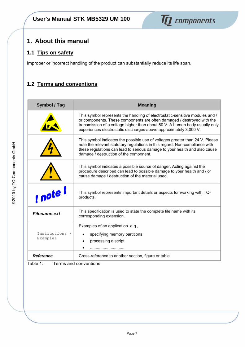
1.2 Terms and conventions
Symbol / Tag Meaning
This symbol represents the handling of electrostatic-sensitive modules and / or components. These components are often damaged / destroyed with the transmission of a voltage higher than about 50 V. A human body usually only experiences electrostatic discharges above approximately 3,000 V.
This symbol indicates the possible use of voltages greater than 24 V. Please note the relevant statutory regulations in this regard. Non-compliance with these regulations can lead to serious damage to your health and also cause damage / destruction of the component.
This symbol indicates a possible source of danger. Acting against the procedure described can lead to possible damage to your health and / or cause damage / destruction of the material used.
This symbol represents important details or aspects for working with TQ-products.
Filename.ext This specification is used to state the complete file name with its corresponding extension.
Instructions / Examples
Examples of an application. e.g.,
• specifying memory partitions • processing a script • ..............................
Reference Cross-reference to another section, figure or table.
©20
10 b
y TQ
-Com
pone
nts
Gm
bH
Table 1: Terms and conventions

User's Manual STK MB5329 UM 100
Page 8
1.3 Handling and ESD tips
General handling of your TQ-products
The TQ-product may only be used and serviced by certified personnel who have taken note of the information, the safety regulations in this document and all related rules and regulations.
A general rule is: not to touch the TQ-product during operation. This is especially important when switching on, changing jumper settings or connecting other devices without ensuring beforehand that the power supply of the system was switched off.
Violation of this guideline may result in damage / destruction of the module and be dangerous to your health.
Improper handling of your TQ-product would render the guarantee invalid.
©2010 by TQ
-Com
ponents Gm
bH
Proper ESD handling
The electronic components of your TQ-product are sensitive to electrostatic discharge (ESD).
Always wear antistatic clothing and use ESD-safe tools, packing materials etc. and operate your TQ-product in an ESD-safe environment. Especially when you switch modules on, change jumper settings, or connect other devices.

User's Manual STK MB5329 UM 100
Page 9
©20
10 b
y TQ
-Co
nent
s G
mbH
m
po
1.4 Registered trademarks
TQ-Components GmbH aims to adhere to the copyrights of all the used graphics and texts in all publications and strives to use original or license-free graphics and texts.
All the brand names and trademarks mentioned in the publication, including those protected by a third party, unless specified otherwise in writing, are subjected to the specifications of the current copyright laws and the proprietary laws of the present registered proprietor without any limitation. One should conclude that brands and trademarks are protected through the rights of a third party.
1.5 Imprint TQ-Components GmbH
Gut Delling, Mühlstraße 2
D-82229 Seefeld Tel.: +49 (0)8153 9308-0 Fax: +49 (0)8153 9308-134
Email: [email protected] Web: http://www.tq-components.com
1.6 Copyright
Copyright protected © 2010 by TQ-Components GmbH.
This manual may not be copied, reproduced, translated, changed or distributed, completely or partially in electronic, machine readable, or in any other form without the written consent of TQ-Components GmbH.
1.7 Disclaimer
TQ-Components GmbH does not guarantee that the information in this manual is up-to-date, correct, complete or of good quality. Nor does TQ-Components assume guarantee for further usage of the information. Liability claims against TQ-Components GmbH, referring to material or idea related damages, caused due to usage or non-usage of the information given in the manual, or caused due to usage of erroneous or incomplete information, are exempted, as long as there is no proven, intentional or negligent fault of TQ-Components GmbH.
TQ-Components GmbH explicitly reserves the rights to change or add to the contents of this manual or parts of it without special notification.

User's Manual STK MB5329 UM 100
Page 10
©2010 by TQ
-Com
ponents Gm
bH
1.8 Copyright and licence expenses
The drivers and utilities for the used components as well as the BIOS are subject to the copyrights of the respective manufacturers. The licence conditions of the respective manufacturer are to be adhered to.
Bootloader-licence expenses are paid by TQ and are included in the price.
Licence expenses for the operating system and applications are not taken into consideration and must be separately calculated / declared.
1.9 Further applicable documents / presumed knowledge
1.9.1 Specifications and manual of the used modules
These documents describe the service, functionality and special characteristics of the used module (incl. BIOS).
1.9.2 Specifications of the used components
The manufacturer's specifications of the used components, for example Compact-Flash cards, are to be taken note of. They contain if applicable additional information, which must be taken note of for safe and reliable operation. These documents are stored at TQ.
1.9.3 General expertise
Expertise in electrical engineering / computer engineering is required for the installation and the use of the device.

User's Manual STK MB5329 UM 100
Page 11
©20
10 b
y TQ
-Com
pone
nts
Gm
bH
1.10 Acronyms and definitions The following terminology and abbreviations are used:
Acronym Meaning BDM Background Debug Mode BGA Ball Grid Array BST Boundary Scan Test CAN Controller Area Network CCR Clock/Control Register CiA CAN in Automation CMOS Complementary Metal Oxide Semiconductor CPU Central Processing Unit DIP Dual In-line Package DVI Digital Visual Interface EEPROM Electrically Erasable Programmable Read-Only Memory EMC Electromagnetic Compatibility ESD ElectroStatic Discharge FEC Fast Ethernet Controller FET Field Effect Transistor GPIO General Purpose Input/Output HD-D-sub High Density D-sub I²C Inter-Integrated Circuit IP00 Ingress Protection 00 JTAG Joint Test Action Group LCD Liquid Crystal Display LED Light Emitting Diode LSB Least Significant Bit LVDS Low Voltage Differential Signal Mbps Mega Bit Per Second MSB Most Significant Bit n.c. Not Connected NC Not Connected OTG On-The-Go PCB Printed Circuit Board ppm Parts Per Million RFU Reserved for Future Use RoHS Restriction of Hazardous Substances RTC Real-Time Clock SDR Single Data Rate SDRAM Synchronous Dynamic Random Access Memory SPI Serial Peripheral Interface TSOP Thin Small Outline Package TSSOP Thin-Shrink Small Outline Package TVS Transient Voltage Suppressor (diode) UART Universal Asynchronous Receiver/Transmitter ULPI UTMI+ Low Pin Interface USB Universal Serial Bus VGA Video Graphics Array WVGA Wide VGA (800 × 480) ZIF Zero Insertion Force
Table 2: Acronyms

User's Manual STK MB5329 UM 100
Page 12
2. Technical description
2.1 Brief description The STK-MB5329 is designed to be powered by TQ modules based on the Freescale ColdFire CPU MCF5329. In combination with the module TQM5329 and a display with touch screen it offers PC core functionalities and standard interfaces.
2.2 System architecture The STK-MB5329 is a compact Starterkit unit with display.
The STK-MB5329 offers the following system interfaces: • 1 × Ethernet 10/100 Mbit/s • 1 × USB host • 1 × USB OTG ©
2010 by TQ-C
omponents G
mbH
• 1 × Serial RS232 • 1 × Serial RS232 or RS485 (optionally) • 1 × CAN 2.0B • 12 × GPIO
2.2.1 Block diagram
TQM
5329
2x 1
20P
ins
CAN
I²C-GPIO
BDM/JTAG
USB-Host USB-OTG
ETH-PHY
ETHRJ45
RS232/RS485RS232 RS232/
RS485
RS232-Treiber
RS232/RS485-Treiber
RS232/RS485-Treiber
Buffer
LCD
Stromver-sorgung
USB Power
Status-LED
Stiftleiste 2-reihig 2x30pol.
Stiftleiste 2-reihig 2x30pol.
Stiftleiste 2-reihig 2x30pol.
Stiftleiste 2-reihig 2x30pol.
SPI Touch-
controller
Touch
Super-visoren
Reset-taster
Puffer-batterie
SVB SV
ULPI-PHY
LCD-BL
GPIO 24 V
Treiber
InterneSchnittstellen
ExterneSchnittstellen
Stromversorgung
Systemkomponenten
Illustration 1: Block diagram STK-MB5329

User's Manual STK MB5329 UM 100
Page 13
©20
10 b
y TQ
mpo
nent
s G
mbH
-Co
3. Electronics specification
3.1 System components
3.1.1 Processor board
The CPU module TQM5329 serves as the central processor unit for the STK-MB5329, which is equipped with the following features:
• Freescale CPU MCF5329 • SDR SDRAM 32 Mbyte • Flash-RAM 16 Mbyte • USBOTG charge pump • Watchdog / RTC / EEPROM • Temperature sensor • Power supply 1.5 V and 3.3 V • Voltage supervision 1.5 V and 3.3 V
3.1.2 Input filter
The STK-MB5329 is equipped with an input filter with an active inverse-polarity protection and a fuse with a rated current of 2.5 A.
3.1.3 Ground concept
There are different reference potentials in the system: • DGND • GND_CAN • GND_RS485_1 • GND_RS485_2
3.1.4 RTC, Watchdog
The RTC and the watchdog are implemented using the Intersil ISL12028.
VBAT voltage range 1.8 V … 5.5 V
Max. current consumption 1.2 µA
Time deviation (with 20 ppm oscillator) ±10 min/year Table 3: Technical parameters RTC
The I²C address of the EEPROM in the ISL12028 is 0b1010111, the address of the clock/control unit is 0b1101111 (address table of I²C bus see Table 6).
User's Manual STK MB5329 UM 100
Page 14
©2010 by TQ
-Com
ponents Gm
bH
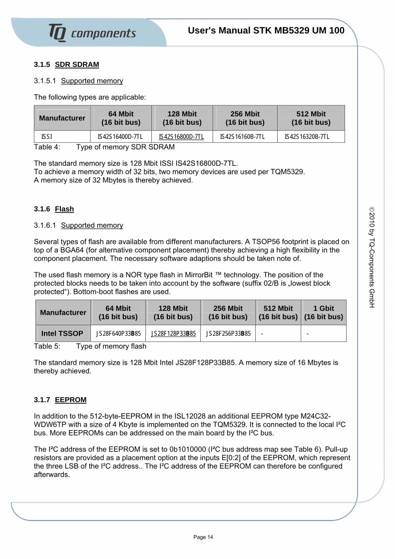
3.1.5 SDR SDRAM
3.1.5.1 Supported memory
The following types are applicable:
Manufacturer 64 Mbit (16 bit bus)
128 Mbit (16 bit bus)
256 Mbit (16 bit bus)
512 Mbit (16 bit bus)
ISSI IS42S16400D-7TL IS42S16800D-7TL IS42S16160B-7TL IS42S16320B-7TL Table 4: Type of memory SDR SDRAM
The standard memory size is 128 Mbit ISSI IS42S16800D-7TL. To achieve a memory width of 32 bits, two memory devices are used per TQM5329. A memory size of 32 Mbytes is thereby achieved.
3.1.6 Flash
3.1.6.1 Supported memory
Several types of flash are available from different manufacturers. A TSOP56 footprint is placed on top of a BGA64 (for alternative component placement) thereby achieving a high flexibility in the component placement. The necessary software adaptions should be taken note of.
The used flash memory is a NOR type flash in MirrorBit ™ technology. The position of the protected blocks needs to be taken into account by the software (suffix 02/B is „lowest block protected“). Bottom-boot flashes are used.
Manufacturer 64 Mbit (16 bit bus)
128 Mbit (16 bit bus)
256 Mbit (16 bit bus)
512 Mbit (16 bit bus)
1 Gbit (16 bit bus)
Intel TSSOP JS28F640P33B85 JS28F128P33B85 JS28F256P33B85 - -
Table 5: Type of memory flash
The standard memory size is 128 Mbit Intel JS28F128P33B85. A memory size of 16 Mbytes is thereby achieved.
3.1.7 EEPROM
In addition to the 512-byte-EEPROM in the ISL12028 an additional EEPROM type M24C32-WDW6TP with a size of 4 Kbyte is implemented on the TQM5329. It is connected to the local I²C bus. More EEPROMs can be addressed on the main board by the I²C bus.
The I²C address of the EEPROM is set to 0b1010000 (I²C bus address map see Table 6). Pull-up resistors are provided as a placement option at the inputs E[0:2] of the EEPROM, which represent the three LSB of the I²C address.. The I²C address of the EEPROM can therefore be configured afterwards.

User's Manual STK MB5329 UM 100
Page 15
©20
10 b
y TQ
-Com
pone
nts
Gm
bH
3.1.8 Temperature sensor
As a temperature sensor a LM73, which is read out via the I²C bus is used.
The I²C address of the sensor is set to 0b1001000 (I²C bus address map see Table 6). A pull-up and a pull-down resistor are provided as a placement option at the input ADDR of the sensor, which influences the two LSB of the I²C address. The I²C address of the sensor can therefore be configured afterwards.
The temperature sensor is placed close to the CPU on the top side of the module.
3.1.9 I²C bus
Table 6 shows the I²C address map. If the device allows the address to be set, corresponding pull-ups and pull-downs are provided at the address inputs.
Device Address range of component Chosen address Remark
USB-OTG MAX3353 0x2C … 0x2D 0x2C (0101 100b) On TQM5329 EEPROM M24C32 0x50 … 0x57 0x50 (1010 000b) On TQM5329 Temperature sensor LM73 0x48 … 0x4A 0x48 (1001 000b) On TQM5329 EEPROM ISL12028 0x57 0x57 (1010 111b) On TQM5329 CCR ISL12028 0x6F 0x6F (1101 111b) On TQM5329 PCA9554D 0x20 … 0x27 0x20 (0100 000b) On STK-MB5329 PCA9554D 0x20 … 0x27 0x21 (0100 001b) On STK-MB5329
Table 6: I²C address map

User's Manual STK MB5329 UM 100
Page 16
3.2 External interfaces
Illustration 2: External interfaces
Attention: destruction or malfunction!
1) Reverse polarity of the input voltage at the power connector (X22) can damage the device! The correct polarity is described under 3.2.1!
2) An identical D-sub connector is used for RS232 (X5, X6A) and CAN (X6B). Incorrect connection is possible!
3) The 15-pin HD-D-sub connector for GPIO (X14) looks like a VGA-monitor output. No monitor may be connected there!
©2010 by TQ
-Com
ponents Gm
bH
3.2.1 Power supply – X22
The supply voltage range of the STK-MB5329 is 24 V DC –37.5% to +25% (15 V to 30 V DC).
A CE-certified DC power supply can be connected via a 2-pin Phoenix connector type MSTBA2,5/2-G-5,08.
Manufacturer Type Description
Phoenix MSTBA2,5/2-G-5,08 Grid 5.08 mm
Max. 250 V, 12 A Table 7: Power supply connector
The plug connector is assigned as follows:
Pin Signal name Remark
1 VCC VCCIN 15 V … 30 V DC 2 GND Ground
Table 8: Pin assignment power supply connector – X22
Notes concerning current load and protection circuit: see 5.1 Power supply.
Please ensure that the power connector is connected to the STK-MB5329 (X22) before connecting the power supply to mains!

User's Manual STK MB5329 UM 100
Page 17
3.2.2 RS232 / RS485 – X5, X6A
The TQM5329 offers up to three UART interfaces. The signals RxD, TxD, RTS# and CTS# are available for all three interfaces.
UART0 is implemented as an RS232 interface. UART1 and UART2 are designed as an RS232 or as galvanically separated RS485. RS232 and RS485 cannot be active simultaneously. Illustration 3 shows the basic circuit of how the UART interfaces of the TQM5329 are connected to the external plug connectors of the STK-MB5329.
For both interfaces a MAX3222 is used as an RS232 driver. For RS485 interfaces a Sipex SP491 is used as a driver. All transceivers are equipped with an integrated ESD protection of up to ±15 kV.
TQM5329
UART0
UART1
UART2
RS232-0-Treiber D-Sub 9 / X6A
RS232-1-Treiber
D-Sub 9 / X5A
D-Sub 9 / X5B
RS232-2-Treiber
©20
10 b
y TQ
-Com
pone
nts
Gm
bH
Illustration 3: Block diagram RS232 / RS485
Table 9 shows the configuration of the 9-pin D-sub connector with RS232 or RS485 signals:
X6A X5A X5B Pin
RS232-0 RS232-1 RS485-1 RS232-2 RS485-2 Description
1 - - Y - Y TX+ (RS485) 2 RXD RXD - RXD - To RS232 transceiver 3 TXD TXD - TXD - From RS232 transceiver 4 - - A - A RX+ (RS485) 5 DGND DGND - DGND - Ground 6 - - Z - Z TX- (RS485) 7 RTS# RTS# - RTS# - From RS232 transceiver 8 CTS# CTS# - CTS# - To RS232 transceiver 9 - - B - B RX- (RS485)
Table 9: Plug connector RS232 / RS485 – X5, X6A
Attention: destruction or malfunction!
Due to four physically identical 9-pin D-sub connectors there is the danger of confusion between RS232, RS485 and CAN. The exact arrangement of the interfaces is shown in Illustration 2.

User's Manual STK MB5329 UM 100
Page 18
3.2.3 CAN – X6B
Depending on the length of the connected cable, the maximum transfer rate is 1 Mbps. The CAN bus can be terminated with 120 Ω by means of DIP switches on the STK-MB5329.
The CAN bus can optionally be galvanically decoupled.
The CAN bus is equipped with a protection circuit. The protection circuit consists of a current-compensated filter and bidirectional protective diodes for CAN LOW and CAN HIGH.
As a plug connector half a dual 9-pin D-sub connector is used. Table 10 shows the pin assignment of the plug connector according to the recommendation of the CiA (CiA Draft standard 102 V2.0):
Pin Signal Type Description
1 - - (Reserved) 2 CAN_L I/O Signal CAN_L 3 CAN_GND P Signal GND 4 - - (Reserved) 5 - - CAN_SHLD (optional) 6 - - GND (optional) 7 CAN_H I/O Signal CAN_H 8 - - (Reserved)
©2010 by TQ
-Com
ponents Gm
bH
9 - P CAN_V+ (optional) Table 10: Plug connector CAN – X6B
Illustration 4: Configuration CAN connector
Attention: destruction or malfunction!
Due to four physically identical 9-pin D-sub connectors there is the danger of confusion between RS232, RS485 and CAN. The exact arrangement of the interfaces is shown in Illustration 2.

User's Manual STK MB5329 UM 100
Page 19
3.2.4 10/100 Mbit Ethernet – X8
An LXT971 is used as a PHY. The device is connected to the TQM5329 via the MII.
Illustration 5: Block diagram Ethernet
©20
10 b
y TQ
-Com
pone
nts
Gm
bH
The following table shows the configuration of the Ethernet plug connector:
Pin Configuration 1 FEC_TPFO+ 2 FEC_TCT 3 FEC_TPFO- 4 FEC_TPFI+ 5 FEC_RCT 6 FEC_TPFI- 7 NC 8 DGND
Table 11: Plug connector Ethernet – X8
Table 12 shows the pull-up and pull-down resistors for configuration of the PHY at the LXT971:
Signal Function Configuration MDDIS Management data disable Disabled SD/TP# Signal detect/twisted pair Twisted-pair mode TXSLEW[0:1] Tx output slew control 11 = 4.4 ns ADDR[0:4] Address 00001 PAUSE Pause during auto negotiation Disabled SLEEP Slow power sleep mode Disabled PWRDWN Power down mode Disabled CFG[1:3] Configuration inputs 111 = auto-neg. enabled / 10/100 / full or half
Table 12: Hardware configuration LXT971
User's Manual STK MB5329 UM 100
Page 20
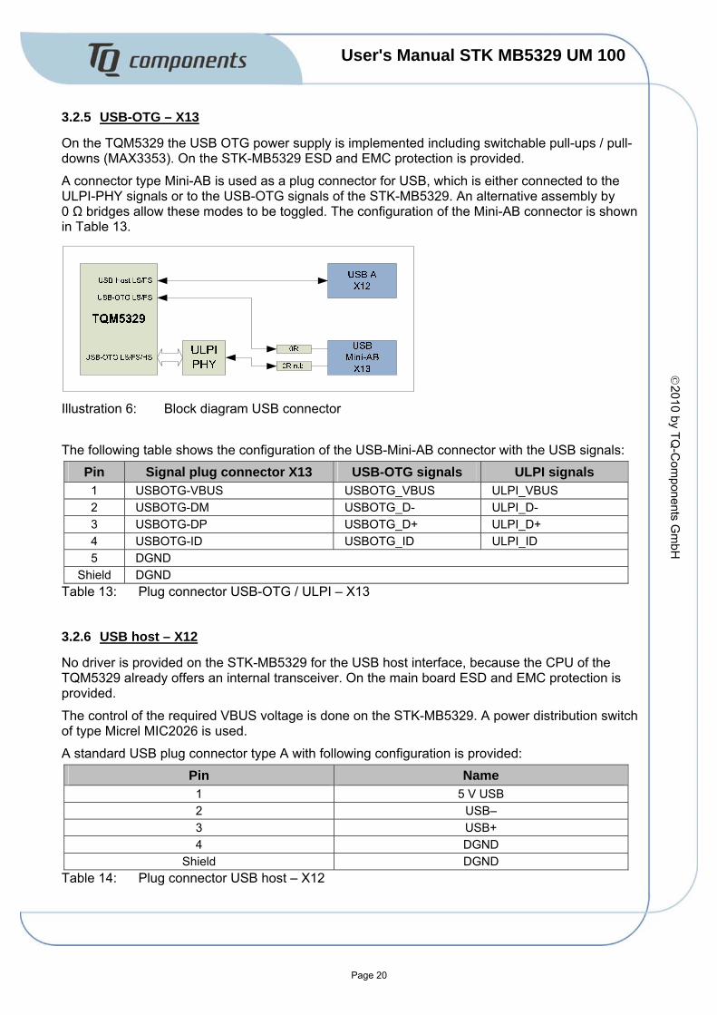
3.2.5 USB-OTG – X13
On the TQM5329 the USB OTG power supply is implemented including switchable pull-ups / pull-downs (MAX3353). On the STK-MB5329 ESD and EMC protection is provided.
A connector type Mini-AB is used as a plug connector for USB, which is either connected to the ULPI-PHY signals or to the USB-OTG signals of the STK-MB5329. An alternative assembly by 0 Ω bridges allow these modes to be toggled. The configuration of the Mini-AB connector is shown in Table 13.
©2010 by TQ
-Com
ponents Gm
bH
Illustration 6: Block diagram USB connector
The following table shows the configuration of the USB-Mini-AB connector with the USB signals:
Pin Signal plug connector X13 USB-OTG signals ULPI signals 1 USBOTG-VBUS USBOTG_VBUS ULPI_VBUS 2 USBOTG-DM USBOTG_D- ULPI_D- 3 USBOTG-DP USBOTG_D+ ULPI_D+ 4 USBOTG-ID USBOTG_ID ULPI_ID 5 DGND
Shield DGND Table 13: Plug connector USB-OTG / ULPI – X13
3.2.6 USB host – X12
No driver is provided on the STK-MB5329 for the USB host interface, because the CPU of the TQM5329 already offers an internal transceiver. On the main board ESD and EMC protection is provided.
The control of the required VBUS voltage is done on the STK-MB5329. A power distribution switch of type Micrel MIC2026 is used.
A standard USB plug connector type A with following configuration is provided: Pin Name
1 5 V USB 2 USB– 3 USB+ 4 DGND
Shield DGND Table 14: Plug connector USB host – X12

User's Manual STK MB5329 UM 100
Page 21
3.2.7 GPIOs – X14
The STK-MB5329 offers eight generals purpose outputs and four general purpose inputs at an external plug connector. The GPIOs are not galvanically separated.
A voltage of 24 V ±20 % supplied to the GPIO plug connector serves as a power supply.
The GPIOs are generated by two 8 bits I²C bus I/O port circuits.
Illustration 7 shows the basic circuit of the GPIO connection on the STK-MB5329. The remaining four I/O ports are made available on an optional header and are additionally connected via a driver to an optional LED.
The digital inputs and outputs are made available via a 15-pin HD-D-sub connector.
©20
10 b
y TQ
-Com
pone
nts
Gm
bH
Illustration 7: Block diagram GPIO

User's Manual STK MB5329 UM 100
Page 22
©2010 by TQ
-Com
ponents Gm
bH
The following table shows the characteristics of the GPIOs:
Parameter Value
Maximum input / output frequency 1 kHz Input voltage UIN 0 V … 24 V ±20 % Input current Typical 1.7 mA Trigger level Uthr(neg), Uthr(pos) 12 V / app. 2 V … 4 V Output voltage 0 / 24 V Max. output current of a single output 0.7 A Max. output current all outputs combined 4 A Type of output driver High side switch (according to SPS standard) Electrical isolation to GND No Common reference potential of inputs and outputs Yes Number of outputs 8 Number of inputs 4
Table 15: Characteristics of the GPIOs
The following table shows the pin assignment of the GPIOs – 15-pin HD-D-sub:
Pin Signal Type Description
1 IN1 I Input 1 2 IN2 I Input 2 3 IN3 I Input 3 4 IN4 I Input 4 5 DGND P Ground 6 VCC24V_EX P Power-input for GPIO 24 V ±20 % 7 DGND P Ground 8 OUT8 O Output 8 9 OUT7 O Output 7
10 OUT6 O Output 6 11 OUT5 O Output 5 12 OUT4 O Output 4 13 OUT3 O Output 3 14 OUT2 O Output 2 15 OUT1 O Output 1
Table 16: Pin assignment GPIO – X14
User's Manual STK MB5329 UM 100
Page 23
©20
10 b
y TQ
-Com
pone
nts
Gm
bH
3.2.7.1 Inputs
The STK-MB5329 offers four digital inputs. The input signals are divided by a resistor divider and routed to the Schmitt trigger inputs of a digital inverter.
The inputs are read via the I²C I/O expander on the main board of the STK-MB5329.
• Interface: I²C • I²C addresses: 0x20 (010 0000b) • I²C addresses: 0x21 (010 0001b) • Protection circuit: TVS diode (bidirectional)
3.2.7.2 Outputs
The STK-MB5329 offers eight digital outputs. The outputs are implemented by a high side driver (STMicroelectronics VN808CM-E), which offers an output current of up to 0.7 A per output. In addition, the driver offers an integrated protective circuit, which protects the outputs against short circuits. All outputs combined may not be loaded with more than 4 A.
The driver is supplied with the voltage, which is fed via the GPIO plug connector (VIN_EX = 24 V ±20 %). The voltage at the driver's outputs can be switched between approx. 0 V and the supply voltage of the device.
The outputs are controlled via the I²C I/O expander on the main board of the STK-MB5329. After a Power-On-Reset all I/O expander ports are configured as inputs. The control signals of the high side driver are therefore pulled to ground with pull-down resistors by default to avoid undefined states after turning on the device.
The driver device offers a status output, to indicate error states in the driver, which can be caused for example by a short circuit at one of the outputs. This status pin can likewise be polled via the I²C I/O expander.
Bidirectional TVS diodes protect against excess voltage-transient at each output.
• Output level: 0 V … 1.4 V (low), VIN_EXT –0.5 V (high) • Current limitation: 0.7 A … 1.4 A
User's Manual STK MB5329 UM 100
Page 24
3.3 Internal interfaces
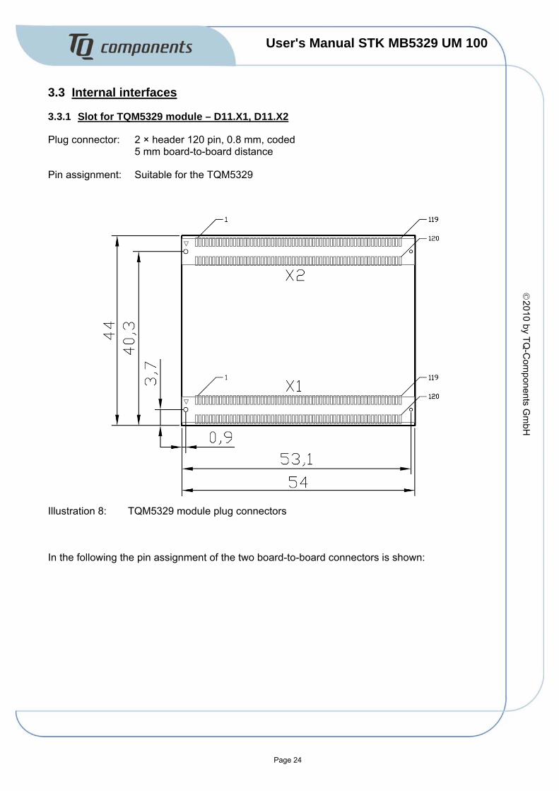
3.3.1 Slot for TQM5329 module – D11.X1, D11.X2
Plug connector: 2 × header 120 pin, 0.8 mm, coded 5 mm board-to-board distance
Pin assignment: Suitable for the TQM5329
©2010 by TQ
-Com
ponents Gm
bH
Illustration 8: TQM5329 module plug connectors
In the following the pin assignment of the two board-to-board connectors is shown:

User's Manual STK MB5329 UM 100
Page 25
©20
10 b
y TQ
-Com
pone
nts
Gm
bH
3.3.1.1 Module plug connector D11.X1
Pin module
Port name module
CPU pin function 1
CPU pin function 2
CPU pin function 3
CPU pin function 4
Dir module Remark
D11.X1-1 RFU - - - - - D11.X1-2 RFU - - - - - D11.X1-3 RFU - - - - - D11.X1-4 FEC_MDIO FEC_MDIO PFECCI2C2 I2C_SDA - I/OPU Ethernet D11.X1-5 GND - - - - P D11.X1-6 FEC_MDC FEC_MDC PFECCI2C3 I2C_SCL - I/OPU-CPU Ethernet D11.X1-7 FEC_TXD3 FEC_TXD3 PFECL7 ULPI_DATA3 - I/OPU D11.X1-8 FEC_TXD2 FEC_TXD2 PFECL6 ULPI_DATA2 - I/OPU D11.X1-9 FEC_TXD1 FEC_TXD1 PFECL5 ULPI_DATA1 - I/OPU D11.X1-10 FEC_TXD0 FEC_TXD0 PFECH5 ULPI_DATA0 - I/OPU
Ethernet/ULPI
D11.X1-11 FEC_TXEN FEC_TXEN PFECH6 - - O Ethernet D11.X1-12 GND - - - - P D11.X1-13 FEC_TXER FEC_TXER PFECL4 - - O D11.X1-14 FEC_TXCLK FEC_TXCLK PFECH7 - - IPU Ethernet
D11.X1-15 GND - - - - P D11.X1-16 FEC_CRS FEC_CRS PFECH0 ULPI_DIR - IPU Ethernet/ULPI D11.X1-17 GND - - - - P D11.X1-18 FEC_COL FEC_COL PFECH4 ULPI_CLK - I/OPU D11.X1-19 FEC_RXD3 FEC_RXD3 PFECL3 ULPI_DATA7 - I/OPU D11.X1-20 FEC_RXD2 FEC_RXD2 PFECL2 ULPI_DATA6 - I/OPU D11.X1-21 FEC_RXD1 FEC_RXD1 PFECL1 ULPI_DATA5 - I/OPU D11.X1-22 FEC_RXD0 FEC_RXD0 PFECH1 ULPI_DATA4 - I/OPU D11.X1-23 FEC_RXDV FEC_RXDV PFECH2 ULPI_STP - IPU
Ethernet/ULPI
D11.X1-24 GND - - - - P D11.X1-25 FEC_RXER FEC_RXER PFECL0 - - IPU Ethernet D11.X1-26 FEC_RXCLK FEC_RXCLK PFECH3 ULPI_NXT - IPU Ethernet/ULPI D11.X1-27 GND - - - - P D11.X1-28 U0CTS# U0CTS# PUARTL3 - - IPU RS232-0 D11.X1-29 GND - - - - P D11.X1-30 U0RTS# U0RTS# PUARTL2 - - O RS232-0 D11.X1-31 RFU - - - - - D11.X1-32 U1CTS# U1CTS# PUARTL7 SSI_BCLK - I/OPU RS232-1 / RS485-1 D11.X1-33 U0RXD U0RXD PUARTL0 - - IPU RS232-0 D11.X1-34 U1RTS# U1RTS# PUARTL6 SSI_FS - I/OPU RS232-1 / RS485-1 D11.X1-35 U0TXD U0TXD PUARTL1 - - O RS232-0 D11.X1-36 GND - - - - P D11.X1-37 U1RXD U1RXD PUARTL4 SSI_RXD - IPU RS232-1 / RS485-1 D11.X1-38 SCL I2C_SCL PFECI2C1 CANTX U2TXD I/OPU I2C D11.X1-39 U1TXD U1TXD PUARTL5 SSI_TXD - O RS232-1 / RS485-1 D11.X1-40 SDA I2C_SDA PFECI2C0 CANRX U2RXD I/OPU I2C D11.X1-41 GND - - - - P D11.X1-42 SSI_FS SSI_FS PSSI2 U2RTS# PWM5 I/OPU RS232-2 / RS485-2 D11.X1-43 SSI_MCLK SSI_MCLK PSSI4 - - I/OPU D11.X1-44 SSI_RXD SSI_RXD PSSI1 U2RXD CANRX IPU D11.X1-45 SSI_TXD SSI_TXD PSSI0 U2TXD CANTX O CAN
D11.X1-46 SSI_BCLK SSI_BCLK PSSI3 U2CTS# PWM7 I/OPU RS232-2 / RS485-2 D11.X1-47 SPI_SOUT QSPI_DOUT PQSPI0 I2C_SDA - I/OPU-CPU Touch D11.X1-48 GND - - - - P D11.X1-49 SPI_SIN QSPI_DIN PQSPI1 U2CTS# - IPU D11.X1-50 SPI_SCK QSPI_CLK PQSPI2 I2C_SCL - I/OPU-CPU Touch
D11.X1-51 SPI_CS1 QSPI_CS1 PQSPI4 PWM7 USBOTG_PU_EN I/O D11.X1-52 SPI_CS2 QSPI_CS2 PQSPI5 U2RTS# - O D11.X1-53 GND - - - - P D11.X1-54 SPI_CS0 QSPI_CS0 PQSPI3 PWM5 - O Touch D11.X1-55 TIN3 DT3IN PTIMER3 DT3OUT U2RXD IPU D11.X1-56 TIN2 DT2IN PTIMER2 DT2OUT U2TXD I/OPU RS232-2 / RS485-2
D11.X1-57 TIN1 DT1IN PTIMER1 DT1OUT DACK1# IPU D11.X1-58 TIN0 DT0IN PTIMER0 DT0OUT DREQ0# IPU D11.X1-59 LCD_PS LCD_PS PLCDCTLL2 - - O D11.X1-60 GND - - - - P D11.X1-61 LCD_REV LCD_REV PLCDCTLL1 - - O D11.X1-62 LCD_LSCLK LCD_LSCLK PLCDCTLL3 - O LCD

User's Manual STK MB5329 UM 100
Page 26
©2010 by TQ
-Com
ponents Gm
bH
Pin module
Port name module
CPU pin function 1
CPU pin function 2
CPU pin function 3
CPU pin function 4
Dir module Remark
D11.X1-63 LCD_SPL_SPR LCD_SPL_SPR PLCDCTLL0 - O D11.X1-64 LCD_CONTRAST LCD_CONTRAST PLCDCTLL6 - O LCD-BL D11.X1-65 GND - - - - P D11.X1-66 LCD_CLS LCD_CLS PLCDCTLL7 - O
D11.X1-67 LCD_FLM LCD_VSYNC
LCD_FLM LCD_VSYNC PLCDCTLL5 - O
D11.X1-68 LCD_ACD LCD_OE
LCD_ACD LCD_OE PLCDCTLH0 - O LCD
D11.X1-69 LCD_LP LCD_HSYNC
LCD_LP LCD_HSYNC PLCDCTLL4 - O
D11.X1-70 LCD_D16 LCD_D16 PLCDDH0 CANRX I/OPU D11.X1-71 LCD_D17 LCD_D17 PLCDDH1 CANTX O LCD
D11.X1-72 GND - - - - P D11.X1-73 LCD_D15 LCD_D15 PLCDDM7 - O D11.X1-74 LCD_D14 LCD_D14 PLCDDM6 - O D11.X1-75 LCD_D13 LCD_D13 PLCDDM5 - O D11.X1-76 LCD_D12 LCD_D12 PLCDDM4 - O
LCD
D11.X1-77 GND - - - - P D11.X1-78 LCD_D10 LCD_D10 PLCDDM2 - O D11.X1-79 LCD_D11 LCD_D11 PLCDDM3 - O D11.X1-80 LCD_D8 LCD_D8 PLCDDM0 - O D11.X1-81 LCD_D9 LCD_D9 PLCDDM1 - O D11.X1-82 LCD_D6 LCD_D6 PLCDDL6 - O D11.X1-83 LCD_D7 LCD_D7 PLCDDL7 - O
LCD
D11.X1-84 GND - - - - P D11.X1-85 LCD_D5 LCD_D5 PLCDDL5 - O D11.X1-86 LCD_D4 LCD_D4 PLCDDL4 - O D11.X1-87 LCD_D3 LCD_D3 PLCDDL3 - O D11.X1-88 LCD_D2 LCD_D2 PLCDDL2 - O
LCD
D11.X1-89 GND - - - - P D11.X1-90 LCD_D0 LCD_D0 PLCDDL0 - O D11.X1-91 LCD_D1 LCD_D1 PLCDDL1 - O LCD
D11.X1-92 A22 A22 - FB_CS4# - O D11.X1-93 A23 A23 - FB_CS5# - O D11.X1-94 A20 A20 - - - O D11.X1-95 A21 A21 - - - O D11.X1-96 GND - - - - P D11.X1-97 A19 A19 - - - O D11.X1-98 A18 A18 - - - O D11.X1-99 A17 A17 - - - O D11.X1-100 A16 A16 - - - O D11.X1-101 GND - - - - P D11.X1-102 A14 A14 - SD_BA0 - O D11.X1-103 A15 A15 - SD_BA1 - O D11.X1-104 A12 A12 - SD_A12 - O D11.X1-105 A13 A13 - SD_A13 - O D11.X1-106 A10 A10 - - O D11.X1-107 A11 A11 - SD_A11 - O D11.X1-108 GND - - - - P D11.X1-109 A9 A9 - SD_A9 - O D11.X1-110 A8 A8 - SD_A8 - O D11.X1-111 A7 A7 - SD_A7 - O D11.X1-112 A6 A6 - SD_A6 - O D11.X1-113 GND - - - - P D11.X1-114 A4 A4 - SD_A4 - O D11.X1-115 A5 A5 - SD_A5 - O D11.X1-116 A2 A2 - SD_A2 - O D11.X1-117 A3 A3 - SD_A3 - O D11.X1-118 A0 A0 - SD_A0 - O D11.X1-119 A1 A1 - SD_A1 - O D11.X1-120 GND - - - - P
Table 17: Module plug connector D11.X1

User's Manual STK MB5329 UM 100
Page 27
©20
10 b
y TQ
-Com
pone
nts
Gm
bH
3.3.1.2 Module plug connector D11.X2
Pin module
Port name module
CPU pin function 1
CPU pin function 2
CPU pin function 3
CPU pin function 4
Dir module Remark
D11.X2-1 VCC3V3 - - - - P D11.X2-2 VCC3V3 - - - - P D11.X2-3 VCC3V3 - - - - P D11.X2-4 VCC3V3 - - - - P D11.X2-5 VCC3V3 - - - - P D11.X2-6 VCC3V3 - - - - P D11.X2-7 VCC3V3 - - - - P D11.X2-8 VBAT - - - - P RTC battery D11.X2-9 GND - - - - P D11.X2-10 GND - - - - P D11.X2-11 GND - - - - P D11.X2-12 GND - - - - P D11.X2-13 GND - - - - P D11.X2-14 GND - - - - P D11.X2-15 GND - - - - P D11.X2-16 GND - - - - P D11.X2-17 GND - - - - P
D11.X2-18 IRQ6# IRQ6# PIRQ6 USBHOST_ VBUS_EN - I/OPU-CPU USB-Host
D11.X2-19 IRQ7# IRQ7# PIRQ7 - - IPU-CPU D11.X2-20 IRQ4# IRQ4# PIRQ4 SSI_MCLK - I/OPU-CPU Touch
D11.X2-21 IRQ5# IRQ5# PIRQ5 USBHOST_ VBUS_OC - IPU-CPU USB-Host
D11.X2-22 IRQ2# IRQ2# PIRQ2 USB_CLKIN - IPU-CPU Ethernet D11.X2-23 IRQ3# IRQ3# PIRQ3 - IPU-CPU Touch D11.X2-24 GND - - - - P D11.X2-25 IRQ1# IRQ1# PIRQ1 DREQ1# SSI_CLKIN IPU-CPU D11.X2-26 RFU - - - - - D11.X2-27 RFU - - - - - D11.X2-28 DDATA2 DDATA2 - - - O BDM D11.X2-29 GND - - - - P D11.X2-30 DDATA0 DDATA0 - - - O D11.X2-31 DDATA3 DDATA3 - - - O D11.X2-32 PST2 PST2 - - - O D11.X2-33 DDATA1 DDATA1 - - - O D11.X2-34 PST0 PST0 - - - O D11.X2-35 PST3 PST3 - - - O
BDM
D11.X2-36 GND - - - - P D11.X2-37 PST1 PST1 - - - O BDM D11.X2-38 JTAG_EN JTAG_EN - - - IPD-CPU BDM/JTAG D11.X2-39 DSCLK DSCLK - TRST# - IPU D11.X2-40 DSI DSI - TDI - IPU BDM/JTAG
D11.X2-41 GND - - - - P D11.X2-42 DSO DSO - TDO - O BDM/JTAG D11.X2-43 RSTIN# - - - IPU D11.X2-44 BKPT# BKPT# - TMS - IPU BDM/JTAG D11.X2-45 RSTOUT# RSTOUT# - - - O D11.X2-46 PSTCLK PSTCLK - TCLK - I/OPU BDM/JTAG D11.X2-47 PORESET# - - - - O D11.X2-48 GND - - - - P D11.X2-49 USBOTG_VBUS - - - - P D11.X2-50 USBOTG_D- USBOTG_M - - - I/O D11.X2-51 USBOTG_ID - - - - I D11.X2-52 USBOTG_D+ USBOTG_P - - - I/O
USB-OTG
D11.X2-53 GND - - - - P D11.X2-54 GND - - - - P D11.X2-55 RFU - - - - - D11.X2-56 USB_D- USBHOST_M - - - I/O USB-Host D11.X2-57 PWM7 PWM7 PPWM7 - - I/OPU Ethernet/ULPI D11.X2-58 USB_D+ USBHOST_P - - - I/O USB-Host D11.X2-59 PWM5 PWM5 PPWM5 - - O LCD-BL D11.X2-60 GND - - - - P D11.X2-61 PWM3 PWM3 PPWM3 DT3OUT DT3IN I/OPU

User's Manual STK MB5329 UM 100
Page 28
©2010 by TQ
-Com
ponents Gm
bH
Pin module
Port name module
CPU pin function 1
CPU pin function 2
CPU pin function 3
CPU pin function 4
Dir module Remark
D11.X2-62 CLKOUT FB_CLK - - - O D11.X2-63 PWM1 PWM1 PPWM1 DT2OUT DT2IN I/OPU D11.X2-64 RFU - - - - - D11.X2-65 GND - - - - P D11.X2-66 CS4# FB_CS4# PCS4 - - O D11.X2-67 CS5# FB_CS5# PCS5 - - O D11.X2-68 CS2# FB_CS2# PCS2 - - O D11.X2-69 CS3# FB_CS3# PCS3 - - O D11.X2-70 CS0# FB_CS0# - - - O D11.X2-71 CS1# FB_CS1# PCS1 - - O D11.X2-72 GND - - - - P D11.X2-73 TA# TA# PBUSCTL2 - - IPU BDM D11.X2-74 R/W# R/W# PBUSCTL1 - - O D11.X2-75 TS# TS# PBUSCTL0 DACK0# - O D11.X2-76 OE# OE# PBUSCTL3 - - O D11.X2-77 GND - - - - P D11.X2-78 BE#/BWE2# BE#/BWE2# PBE2 SD_DQM2# - O D11.X2-79 BE#/BWE3# BE#/BWE3# PBE3 SD_DQM3# - O D11.X2-80 BE#/BWE0# BE#/BWE0# PBE0 SD_DQM0# - O D11.X2-81 BE#/BWE1# BE#/BWE1# PBE1 SD_DQM1# - O D11.X2-82 D30 D30 - SD_D30 - I/OPU D11.X2-83 D31 D31 - SD_D31 - I/OPU D11.X2-84 GND - - - - P D11.X2-85 D29 D29 - SD_D29 - I/OPU D11.X2-86 D28 D28 - SD_D28 - I/OPU D11.X2-87 D27 D27 - SD_D27 - I/OPU D11.X2-88 D26 D26 - SD_D26 - I/OPU D11.X2-89 GND - - - - P D11.X2-90 D24 D24 - SD_D24 - I/OPU D11.X2-91 D25 D25 - SD_D25 - I/OPU D11.X2-92 D22 D22 - SD_D22 - I/OPU D11.X2-93 D23 D23 - SD_D23 - I/OPU D11.X2-94 D20 D20 - SD_D20 - I/OPU D11.X2-95 D21 D21 - SD_D21 - I/OPU D11.X2-96 GND - - - - P D11.X2-97 D19 D19 - SD_D19 - I/OPU D11.X2-98 D18 D18 - SD_D18 - I/OPU D11.X2-99 D17 D17 - SD_D17 - I/OPU D11.X2-100 D16 D16 - SD_D16 - I/OPU D11.X2-101 GND - - - - P D11.X2-102 D14 D14 - FB_D30 - I/OPU D11.X2-103 D15 D15 - FB_D31 - I/OPU D11.X2-104 D12 D12 - FB_D28 - I/OPU D11.X2-105 D13 D13 - FB_D29 - I/OPU D11.X2-106 D10 D10 - FB_D26 - I/OPU D11.X2-107 D11 D11 - FB_D27 - I/OPU D11.X2-108 GND - - - - P D11.X2-109 D9 D9 - FB_D25 - I/OPU D11.X2-110 D8 D8 - FB_D24 - I/OPU D11.X2-111 D7 D7 - FB_D23 - I/OPU D11.X2-112 D6 D6 - FB_D22 - I/OPU D11.X2-113 GND - - - - P D11.X2-114 D4 D4 - FB_D20 - I/OPU D11.X2-115 D5 D5 - FB_D21 - I/OPU D11.X2-116 D2 D2 - FB_D18 - I/OPU D11.X2-117 D3 D3 - FB_D19 - I/OPU D11.X2-118 D0 D0 - FB_D16 - I/OPU D11.X2-119 D1 D1 - FB_D17 - I/OPU D11.X2-120 GND - - - - P
Table 18: Module plug connector D11.X2

User's Manual STK MB5329 UM 100
Page 29
©20
10 b
y TQ
-Com
pone
nts
Gm
bH
Signals used on STK-MB5329 Power BDM/JTAG-Interface
Table 19: Legend colours TQM5329
3.3.1.3 TQM5329 signals on headers X1, X2, X3, X4
All signals of the TQM5329, except those of the USB data lines, are led optionally on a double row 60-pin header with 2.54 mm grid. The headers X1 and X2 are next to module plug connector D11.X1, the headers X3 and X4 are next to module plug connector D11.X2. The headers are as assigned follows:

User's Manual STK MB5329 UM 100
Page 30
©2010 by TQ
-Com
ponents Gm
bH
3.3.1.3.1 Header X1
Module Signal X1 Signal Module
D11.X1-1 RFU 1 2 RFU D11.X1-3 D11.X1-5 GND 3 4 FEC0_TXD3 D11.X1-7 D11.X1-9 FEC0_TXD1 5 6 FEC0_TXEN D11.X1-11 D11.X1-13 FEC0_TXER 7 8 GND D11.X1-15 D11.X1-17 GND 9 10 FEC0_RXD3 D11.X1-19 D11.X1-21 FEC0_RXD1 11 12 FEC0_RXDV D11.X1-23 D11.X1-25 FEC0_RXER 13 14 GND D11.X1-27 D11.X1-29 GND 15 16 RFU D11.X1-31 D11.X1-33 U0RXD 17 18 U0TXD D11.X1-35 D11.X1-37 U1RXD 19 20 U1TXD D11.X1-39 D11.X1-41 GND 21 22 SSI_MCLK D11.X1-43 D11.X1-45 SSI_TXD 23 24 SPI_SOUT D11.X1-47 D11.X1-49 SPI_SIN 25 26 SPI_CS1 D11.X1-51 D11.X1-53 GND 27 28 TIN3 D11.X1-55 D11.X1-57 TIN1 29 30 LCD_PS D11.X1-59 D11.X1-61 LCD_REV 31 32 LCD_SPL_SPR D11.X1-63 D11.X1-65 GND 33 34 LCD_FLM/LCD_VSYNC D11.X1-67 D11.X1-69 LCD_LP/LCD_HSYNC 35 36 LCD_D17 D11.X1-71 D11.X1-73 LCD_D15 37 38 LCD_D13 D11.X1-75 D11.X1-77 GND 39 40 LCD_D11 D11.X1-79 D11.X1-81 LCD_D9 41 42 LCD_D7 D11.X1-83 D11.X1-85 LCD_D5 43 44 LCD_D3 D11.X1-87 D11.X1-89 GND 45 46 LCD_D1 D11.X1-91 D11.X1-93 A23/CS5# 47 48 A21 D11.X1-95 D11.X1-97 A19 49 50 A17 D11.X1-99 D11.X1-101 GND 51 52 A15 D11.X1-103 D11.X1-105 A13 53 54 A11 D11.X1-107 D11.X1-109 A9 55 56 A7 D11.X1-111 D11.X1-113 GND 57 58 A5 D11.X1-115 D11.X1-117 A3 59 60 A1 D11.X1-119
Table 20: Module signals, header – X1

User's Manual STK MB5329 UM 100
Page 31
©20
10 b
y TQ
-Com
pone
nts
Gm
bH
3.3.1.3.2 Header X2
Module Signal X2 Signal Module
D11.X1-2 RFU 1 2 FEC0_MDIO D11.X1-4 D11.X1-6 FEC0_MDC 3 4 FEC0_TXD2 D11.X1-8 D11.X1-10 FEC0_TXD0 5 6 GND D11.X1-12 D11.X1-14 FEC0_TXCLK 7 8 FEC0_CRS D11.X1-16 D11.X1-18 FEC0_COL 9 10 FEC0_RXD2 D11.X1-20 D11.X1-22 FEC0_RXD0 11 12 GND D11.X1-24 D11.X1-26 FEC0_RXCLK 13 14 U0CTS# D11.X1-28 D11.X1-30 U0RTS# 15 16 U1CTS# D11.X1-32 D11.X1-34 U1RTS# 17 18 GND D11.X1-36 D11.X1-38 SCL 19 20 SDA D11.X1-40 D11.X1-42 SSI_FS 21 22 SSI_RXD D11.X1-44 D11.X1-46 SSI_BCLK 23 24 GND D11.X1-48 D11.X1-50 SPI_SCK 25 26 SPI_CS2 D11.X1-52 D11.X1-54 SPI_CS0 27 28 TIN2 D11.X1-56 D11.X1-58 TIN0 29 30 GND D11.X1-60 D11.X1-62 LCD_LSCLK 31 32 LCD_CONTRAST D11.X1-64 D11.X1-66 LCD_CLS 33 34 LCD_ACD/ LCD_OE D11.X1-68 D11.X1-70 LCD_D16 35 36 GND D11.X1-72 D11.X1-74 LCD_D14 37 38 LCD_D12 D11.X1-76 D11.X1-78 LCD_D10 39 40 LCD_D8 D11.X1-80 D11.X1-82 LCD_D6 41 42 GND D11.X1-84 D11.X1-86 LCD_D4 43 44 LCD_D2 D11.X1-88 D11.X1-90 LCD_D0 45 46 A22 D11.X1-92 D11.X1-94 A20 47 48 GND D11.X1-96 D11.X1-98 A18 49 50 A16 D11.X1-100 D11.X1-102 A14 51 52 A12 D11.X1-104 D11.X1-106 A10 53 54 GND D11.X1-108 D11.X1-110 A8 55 56 A6 D11.X1-112 D11.X1-114 A4 57 58 A2 D11.X1-116 D11.X1-118 A0 59 60 GND D11.X1-120
Table 21: Module signals, header – X2

User's Manual STK MB5329 UM 100
Page 32
©2010 by TQ
-Com
ponents Gm
bH
3.3.1.3.3 Header X3
Modul Signal X3 Signal Modul
D11.X2-1 VCC3V3 1 2 VCC3V3 D11.X2-3 D11.X2-5 VCC3V3 3 4 VCC3V3 D11.X2-7 D11.X2-9 GND 5 6 GND D11.X2-11 D11.X2-13 GND 7 8 GND D11.X2-15 D11.X2-17 GND 9 10 IRQ7# D11.X2-19 D11.X2-21 IRQ5# 11 12 IRQ3# D11.X2-23 D11.X2-25 IRQ1# 13 14 RFU D11.X2-27 D11.X2-29 GND 15 16 DTATA3 D11.X2-31 D11.X2-33 DTATA1 17 18 PST3 D11.X2-35 D11.X2-37 PST1 19 20 DSCLK D11.X2-39 D11.X2-41 GND 21 22 RST_IN# D11.X2-43 D11.X2-45 RST_OUT# 23 24 PORESET# D11.X2-47 D11.X2-49 USBOTG_VBUS 25 26 USBOTG_ID D11.X2-51 D11.X2-53 GND 27 28 RFU D11.X2-55 D11.X2-57 PWM7 29 30 PWM5 D11.X2-59 D11.X2-61 PWM3 31 32 PWM1 D11.X2-63 D11.X2-65 GND 33 34 CS5# D11.X2-67 D11.X2-69 CS3# 35 36 CS1# D11.X2-71 D11.X2-73 TA# 37 38 TS# D11.X2-75 D11.X2-77 GND 39 40 BE#/BWE3# D11.X2-79 D11.X2-81 BE#/BWE1# 41 42 D31 D11.X2-83 D11.X2-85 D29 43 44 D27 D11.X2-87 D11.X2-89 GND 45 46 D25 D11.X2-91 D11.X2-93 D23 47 48 D21 D11.X2-95 D11.X2-97 D19 49 50 D17 D11.X2-99 D11.X2-101 GND 51 52 D15 D11.X2-103 D11.X2-105 D13 53 54 D11 D11.X2-107 D11.X2-109 D9 55 56 D7 D11.X2-111 D11.X2-113 GND 57 58 D5 D11.X2-115 D11.X2-117 D3 59 60 D1 D11.X2-119
Table 22: Module signals, header – X3

User's Manual STK MB5329 UM 100
Page 33
©20
10 b
y TQ
-Com
pone
nts
Gm
bH
3.3.1.3.4 Header X4
Module Signal X4 Signal Module
D11.X2-2 VCC3V3 1 2 VCC3V3 D11.X2-4 D11.X2-6 VCC3V3 3 4 VBAT D11.X2-8 D11.X2-10 GND 5 6 GND D11.X2-12 D11.X2-14 GND 7 8 GND D11.X2-16 D11.X2-18 IRQ6# 9 10 IRQ4# D11.X2-20 D11.X2-22 IRQ2# 11 12 GND D11.X2-24 D11.X2-26 RFU 13 14 DDATA2 D11.X2-28 D11.X2-30 DDATA0 15 16 PST2 D11.X2-32 D11.X2-34 PST0 17 18 GND D11.X2-36 D11.X2-38 JTAG_EN 19 20 DSI D11.X2-40 D11.X2-42 DSO 21 22 BKPT# D11.X2-44 D11.X2-46 PSTCLK 23 24 GND D11.X2-48 D11.X2-50 RFU 25 26 RFU D11.X2-52 D11.X2-54 GND 27 28 RFU D11.X2-56 D11.X2-58 RFU 29 30 GND D11.X2-60 D11.X2-62 CLKOUT 31 32 RFU D11.X2-64 D11.X2-66 CS4# 33 34 CS2# D11.X2-68 D11.X2-70 CS0# 35 36 GND D11.X2-72 D11.X2-74 R/W# 37 38 OE# D11.X2-76 D11.X2-78 BE#/BWE2# 39 40 BE#/BWE0# D11.X2-80 D11.X2-82 D30 41 42 GND D11.X2-84 D11.X2-86 D28 43 44 D26 D11.X2-88 D11.X2-90 D24 45 46 D22 D11.X2-92 D11.X2-94 D20 47 48 GND D11.X2-96 D11.X2-98 D18 49 50 D16 D11.X2-100 D11.X2-102 D14 51 52 D12 D11.X2-104 D11.X2-106 D10 53 54 GND D11.X2-108 D11.X2-110 D8 55 56 D6 D11.X2-112 D11.X2-114 D4 57 58 D2 D11.X2-116 D11.X2-118 D0 59 60 GND D11.X2-120
Table 23: Module signals, header – X4

User's Manual STK MB5329 UM 100
Page 34
©2010 by TQ
-Com
ponents Gm
bH
3.3.2 Connectors for LCD – X15, X16
The connection of the LCD is carried out via an 18 bit (6 bit red, 6 bit green, 6 bit blue) CMOS interface. Neither LVDS nor DVI displays are directly supported. The following plug connector is used: Yamaichi, FPC-98210-4021, 40-pin ZIF connector. Depending on the display used it is either connected via X15 (PowerView and CPT) or X16 (Admatec).
X15 X16 Signal Type Description 18 bit 1 – VCC3V3 – VCC3V3 2 – VCC3V3 – VCC3V3 3 – VCC3V3 – VCC3V3 4 37 VCC3V3 – VCC3V3 5 38 n.c. – No Connection 6 39 Display Enable O DRDY → 22R, direct from TQMa31 7 40 Ground – DGND 8 – n.c. – No Connection 9 35 Ground – DGND 10 34 n.c. – No Connection 11 32 Ground – DGND 12 30 Blue 5 (MSB) O IPP_DO_DISPB_DATA[5] → 22R, direct from TQMa31 B5 13 29 Blue 4 O IPP_DO_DISPB_DATA[4] → 22R, direct from TQMa31 B4 14 28 Blue 3 O IPP_DO_DISPB_DATA[3] → 22R, direct from TQMa31 B3 15 27 Ground – DGND 16 26 Blue 2 O IPP_DO_DISPB_DATA[2] → 22R, direct from TQMa31 B2 17 25 Blue 1 O IPP_DO_DISPB_DATA[1] → 22R, direct from TQMa31 B1 18 24 Blue 0 (LSB) O IPP_DO_DISPB_DATA[0] → 22R, direct from TQMa31 B0 19 23 Ground – DGND 20 22 Green 5 (MSB) O IPP_DO_DISPB_DATA[11] → 22R, direct from TQMa31 G5 21 21 Green 4 O IPP_DO_DISPB_DATA[10] → 22R, direct from TQMa31 G4 22 20 Green 3 O IPP_DO_DISPB_DATA[9] → 22R, direct from TQMa31 G3 23 19 Ground – DGND 24 18 Green 2 O IPP_DO_DISPB_DATA[8] → 22R, direct from TQMa31 G2 25 17 Green 1 O IPP_DO_DISPB_DATA[7] → 22R, direct from TQMa31 G1 26 16 Green 0 (LSB) O IPP_DO_DISPB_DATA[6] → 22R, direct from TQMa31 G0 27 15 Ground – DGND 28 14 Red 5 (MSB) O IPP_DO_DISPB_DATA[17] → 22R, direct from TQMa31 R5 29 13 Red 4 O IPP_DO_DISPB_DATA[16] → 22R, direct from TQMa31 R4 30 12 Red 3 O IPP_DO_DISPB_DATA[15] → 22R, direct from TQMa31 R3 31 11 Ground – DGND 32 10 Red 2 O IPP_DO_DISPB_DATA[14] → 22R, direct from TQMa31 R2 33 9 Red 1 O IPP_DO_DISPB_DATA[13] → 22R, direct from TQMa31 R1 34 8 Red 0 (LSB) O IPP_DO_DISPB_DATA[12] → 22R, direct from TQMa31 R0 35 7 n.c. – No Connection 36 5 Ground – DGND 37 4 Ground – DGND 38 3 DCLK O FPSHIFT → 22R, direct from TQMa31 39 2 Ground – DGND 40 1 Ground – DGND – 6 n.c. – 31 n.c. – 33 n.c. – 36 n.c.
# - low active signal, ↑ - element to VCC (pull up), ↓ - element to ground (pull down), → element in series Table 24: Pin assignment LCD plug connectors X15, X16
User's Manual STK MB5329 UM 100
Page 35
©20
10 b
y TQ
-Com
pone
nts
Gm
bH
3.3.3 Backlight connectors – X19, X20
The following plug connector is used: JST, SM02B-BHSS-1-TB, 2-pin, single row, 90° bent
The following table shows the pin assignment of the backlight connector:
Pin Signal Type Description
1 VLEDA - LED anode
2 VLEDC - LED cathode
# - low active signal, ↑ - element to VCC (pull up), ↓ - element to ground (pull down), → element in series
Table 25: Pin assignment backlight – X21
3.3.4 Touch screen connectors – X17, X18
The following plug connector is used: JST, SM02B-BHSS-1-TB, 2-pin, single row, 90° bent.
The STK-MB5329 supports the types of touch panel listed in the following table. The table also includes the pin assignment of the touch connectors X17 and X18.
Signal X17 Admatec RTP070F13N
X18 DMC AST-070A080A
Touch_L 3 4
Touch_R 1 2
Touch_T 2 3
Touch_B 4 1 Table 26: Pin assignment touch screen – X17, X18

User's Manual STK MB5329 UM 100
Page 36
©2010 by TQ
-Com
ponents Gm
bH
3.3.5 BDM / JTAG Debug ports – X21, X10
To connect a JTAG debugger for the MCF5329 on the TQM5329 a 14-pin header is used – X10. The JTAG interface is a subset of the BDM interface. To switch between BDM and JTAG mode, a 10 kΩ pull-up resistor to VDD is provided. In the default configuration of the STK-MB5329 BDM is active. The following table shows the pin assignment of the JTAG debugger.
Pin Signal Type Description
1 DSO/TDO O JTAG Test Data Out 2 NC Not connected 3 DSI/TDI I JTAG Test Data In, Pull-Up on TQM5329 4 DSCLK/TRST# I JTAG Test Reset, Pull-Up on TQM5329 5 NC Not connected 6 VCC3V3 P Power Out via 220 Ohm 7 PSTCLK/TCLK I JTAG Test Clock, Pull-Up on TQM5329 8 NC Not connected 9 BKPT#/TMS I JTAG Test Mode Select, Pull-Up on TQM5329 10 NC Not connected 11 NC Not connected 12 DGND P Digital Ground 13 RESIN# I Reset In (Hard Reset), Pull-Up on TQM5329 14 NC Not connected 15 NC Not connected 16 DGND P Digital Ground
Table 27: Pin assignment JTAG debugger – X10
The following table shows the pin assignment of the BDM debugger.
Pin Signal Type Description
1 TCK I Clock Signal 2 DGND - Signal Ground 3 TDO O Data from device 4 VCC (TRGT) - Target power supply 5 TMS I JTAG state machine control 6 n.c. - Reserved 7 n.c. - Reserved 8 n.c. - Reserved 9 TDI I Data to device 10 DGND - Signal ground
Table 28: Pin assignment BDM debugger – X21

User's Manual STK MB5329 UM 100
Page 37
3.4 User's interfaces
3.4.1 Display
The STK-MB5329 comes with a 7" WVGA LCD in a separate housing. The maximum resolution of the display is 800 × 480 pixels.
Different display modules are provided for the use in combination with the STK-MB5329.
3.4.2 Touch screen
The display unit of the STK-MB5329 offers an integrated 4-wire touch screen, which allows inputs via a graphical interface. The touch screen has a horizontal resolution of 0.21 mm and a vertical resolution of 0.15 mm.
Attention: destruction or malfunction!
The touch screen may only be operated with fingers or specially designed pens. No sharp or pointed objects may be used, as they may damage the touch screen!
©20
10 b
y TQ
-Co
nent
s G
mbH
mpo 3.4.3 Reset button – S1
To be able to reset the STK-MB5329 at any time to a defined state, a reset button is available at the connector panel.
3.4.4 Indicator LEDs
A blue LED serves to display the correct function of the supply voltages.
The plug connector of the Ethernet interface offers two status LEDs.
Name / Function LED Remark
Power On LED blue VCC3V3 / VCC5V GPIO internal LED yellow GPIO[4 … 7] Ethernet LED green Link Status / Activity Ethernet LED yellow Speed
Table 29: Overview LEDs

User's Manual STK MB5329 UM 100
Page 38
3.4.5 DIP switches
The STK-MB5329 is equipped with six DIP switches whose functions are shown in the following table:
Switch Function S2 – 1 Termination 120 Ω CAN S2 – 2 Not used S4 – 1 Termination 120 Ω RS485-1_A/B S4 – 2 Termination 120 Ω RS485-1_Y/Z S3 – 1 Termination 120 Ω RS485-2_A/B S3 – 2 Termination 120 Ω RS485-2_Y/Z
Table 30: Function DIP switches
3.5 Battery To supply the RTC of the STK-MB5329, a lithium battery with very low self-discharge is used. The battery is socketed and can therefore be easily exchanged.
©2010 by TQ
-Com
ponents Gm
bH
Manufacturer Type Description Sony CR2032 Lithium battery, typical capacity approx. 200 mAh / 3 V
Table 31: RTC battery
The battery is protected against reverse polarity and overload with a resistor of 1 kΩ in series to the battery. The battery has a product life of approx. 650 h with a discharge current of 0.3 mA. The RTC located on the module needs a maximum current of 1.2 µA. Hence, only the self-discharge of the battery is authoritative for the battery life's consideration.
Attention: destruction or malfunction!
Reverse polarity of the battery can damage or destroy the device. Attention must be paid to the correct polarity of the battery.
4. Mechanics specification
4.1 Dimensions mainboard Dimensions Details
Outer dimensions (L × W) 175 mm × 120 mm (plus protruding plug connectors) Printed circuit board thickness Max. 2 mm Max component height top side 10 mm and 29 mm Max component height bottom side 4 mm
Table 32: Mechanical data
4.2 Component placement diagrams The component placement diagrams of the top and the bottom side are displayed in the following.

User's Manual STK MB5329 UM 100
Page 39
4.2.1 Mainboard – component placement top
©20
10 b
y TQ
-Com
pone
nts
Gm
bH
Illustration 9: Mainboard – component placement top

User's Manual STK MB5329 UM 100
Page 40
4.2.2 Mainboard – component placement bottom
©2010 by TQ
-Com
ponents Gm
bH
Illustration 10: Mainboard – component placement bottom

User's Manual STK MB5329 UM 100
Page 41
©20
10 b
y TQ
pone
nts
Gm
bH
-Com
5. Technical data
5.1 Power supply
Function Details
Input voltage 15 V - 30 V DC (corresponds to 24 V DC, -37.5 % … +25 %) The voltage is measured directly at the power connector of the STK-MB5329.
Input current Supply: U = 18 V, I = 240 mA Power consumption Ptyp = 4.3 W Reverse voltage protection Yes, actively via serial FET (max. 32 V for both polarities allowed)
Excess voltage protection No. At an excess voltage of more than 32 V DC the supply has to switch off within 1 ms.
Filter Integrated filters for the power supply input. Table 33: Power supply specification
The specified standard power supply for the STK-MB5329 is the following:
• IPCX86MM NT REV.100 => 18 V (max. 3.9 A) (The DC supply cord is prefabricated suitable for iPCbox EX and IPCG3)
With the abovementioned power supply the low voltage directives according to EN 60950 are met. In the case where another power supply is used or if the device is supplied from a 24 V power grid, it is the customers responsibility to make sure the specified maximum ratings and standards are met.
5.2 Vibration load
Parameter Details
Oscillation, sinusoidal According to DIN EN 60068-2-6 Frequency ranges 2 – 9 Hz, 9 – 200 Hz, 200 – 500 Hz Wobble rate 1.0 octaves / min Excitation axes X-Y-Z axis
Amplitude 2 Hz … 9 Hz: 3.5 ms-2 9 Hz … 200 Hz: 10 ms-2 200 Hz … 500 Hz: 15 ms-2
Table 34: Vibration test requirements
5.3 Shock load
Parameter Details
Shocks According to DIN EN 60068-2-27 Shock form Half sine Acceleration 30 g Residence time 10 ms Number of shocks 3 shocks per direction Excitation axes 6X, 6Y, 6Z
Table 35: Shock test requirements

User's Manual STK MB5329 UM 100
Page 42
©2010 by TQ
-Com
ponents Gm
bH
6. Safety requirements and protective regulations
6.1 Operational safety and personal security
A separate test can be omitted on account of the occurring voltages (≤35 V DC).
6.2 Environment protection
By environmentally friendly processes, production equipment and products, we contribute to the protection of our environment.
To be able to reuse the product, it is produced in such a way (a modular construction) that it can be easily repaired and disassembled.
The energy consumption of this subassembly is minimised by suitable measures.
Printed pc-boards are delivered in reusable packaging. Modules and devices are delivered in an outer packaging of paper, cardboard or other recyclable material.
Due to technical reasons a battery is necessary for this project. Batteries containing mercury (Hg), cadmium (Cd) or lead (Pb) are not used. To allow a separate disposal, batteries are generally only mounted in sockets.
No use of PCB containing capacitors and transformers (polychlorinated biphenyls).
These points are an essential part of the following laws:
• The law to encourage the circular flow economy and assurance of the environmentally acceptable removal of waste as at 27.9.94 (source of information: BGBl I 1994, 2705)
• Regulation with respect to the utilization and proof of removal as at 1.9.96 (source of information: BGBl I 1996, 1382, (1997, 2860)
• Regulation with respect to the avoidance and utilization of packaging waste as at 21.8.98 (source of information: BGBl I 1998, 2379)
• Regulation with respect to the European Waste Directory as at 1.12.01 (source of information: BGBl I 2001, 3379)

User's Manual STK MB5329 UM 100
Page 43
©20
10 b
y T
mpo
nent
s G
mbH
Q-C
o
6.2.1 RoHS compliance
The STK-MB5329 is manufactured RoHS compliant.
• All used components and assemblies are RoHS compliant • RoHS compliant soldering processes are used
7. Climatic and operational conditions
• Ambient temperature: − Standard temperature range: 0 °C … +50 °C − Extended temperature range: –30 °C … +70 °C
• Relative air humidity (operation / storing): 10 % … 90 % (not condensing)
• Protection class: IP00
7.1 Reliability and product life
The device is designed for a product life of approx. 40,000 hrs @ +40 °C, excepting the lithium cell, which should be renewed after approximately 3 years.
7.1.1 Interfaces and plug connectors
Plug connectors of middle grade, which guarantee at least 100 mating cycles are used for all external accessible interfaces.
Please ensure that the power connector is connected to the STK-MB5329 (X22) before connecting the power supply to mains!
8. Software: Supported software: µC Linux 2.6.


![TQ - bonfiglioli.com (Drive Service ... nominal torque Mn 2 [nm] TQ 060 TQ 070 TQ 090 TQ 130 TQ 160 30 70 200 400 800. 7 IP65 degree protection universal design ... no matter where](https://img.pdfslide.us/doc/110x75/5addd7837f8b9a213e8d4fa6/tq-drive-service-nominal-torque-mn-2-nm-tq-060-tq-070-tq-090-tq-130-tq.jpg)