Embed Size (px)
Citation preview
User’s Manual of Board Microcontroller CP-JR ARM7 LPC2368
ETT CO.,LTD. -1- WWW.ETT.CO.TH
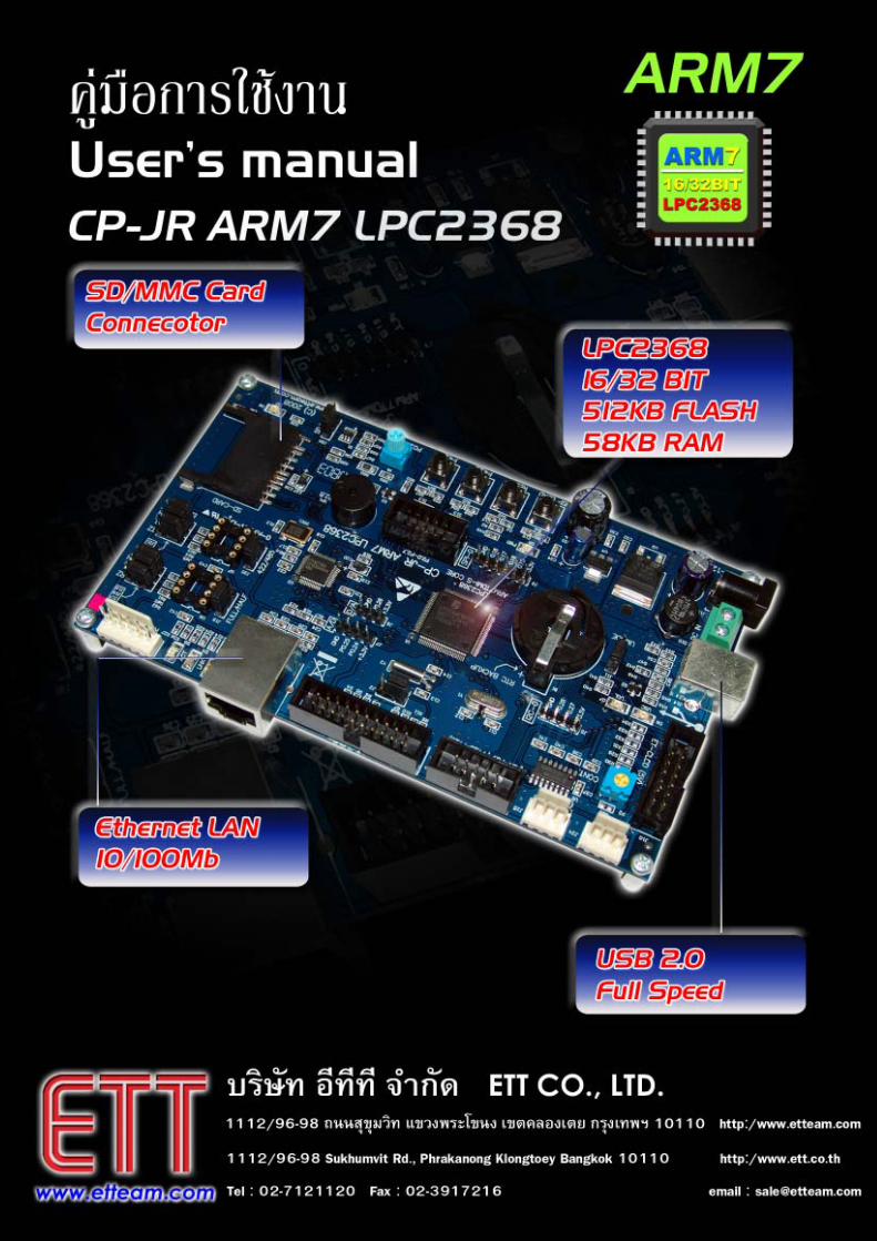
CP-JR ARM7 LPC2368
CP-JR ARM7 LPC2368 is ARM7TDMI-S Core Board
Microcontroller that uses 16/32-Bit 100 Pin (LQFP) Microcontroller No.LPC2368 from Philips (NXP). All resources inside LPC2368 is quite perfect, so it is the most suitable to learn and study because if user can learn and understand the applications of all resources inside MCU well, it makes user can modify, apply and develop many excellent applications in the future. Because Hardware system of LPC2368 includes the necessary devices within only one MCU such as USB, Ethernet, SD/MMC Memory Card, ADC, DAC, Timer/Counter, PWM, Capture, I2C, SPI, UART, and etc.
So, ETT Team tries to find out and research the
detailed information of LPC2368 and design it to be Board Microcontroller version “CP-JR ARM7 LPC2368”. We hope that user will buy this device to learn, modify, and develop application in the future as desired under the reasonable price. The main purpose of designing this Board CP-JR ARM7 LPC2368 is to be able to support both users who want to learn, study or try device and including person who want to really modify and develop devices. The structure of board consists of the basic components that are necessary to learn and test such as LED to display Output Logic, Push Button Switch to test Logic Input, Volume
User’s Manual of Board Microcontroller CP-JR ARM7 LPC2368
ETT CO.,LTD. -2- WWW.ETT.CO.TH
to adjust voltage to test A/D, and Mini Speaker to generate various Beep sound. Moreover, it provides other devices in the high level to support the applications such as Port USB, SD/MMC Memory Card, Port Ethernet LAN, Dot-Matrix LCD, RS232, RS232, RS422/485. Furthermore, there is available GPIO; it makes user can design and use it with other devices as desired. So, CP-JR ARM7 LPC2368 is one of the most interesting multi-purpose boards.
Specifications of Board
1. Use 16/32 Bit ARM7TDMI-S MCU No.LPC2368 from Philips (NXP)
2. Has 512KB Flash Memory and 58KB Static RAM internal MCU
3. Use 12.00MHz Crystal, so MCU can process data with the maximum high speed at 72MHz when using it with Phase-Locked Loop (PLL) internal MCU.
4. Has RTC Circuit (Real Time Clock) with 32.768KHz XTAL and Battery Backup
5. Support In-System Programming (ISP) and In-Application Programming (IAP) through On-Chip Boot-Loader Software via Port UART-0 (RS232)
6. Has circuit to connect with standard 20 Pin JTAG ARM for Real Time Debugging
7. 7-12 VAC/DC Power Supply uses Connector type as Terminal and DC-Jack with Bridge Rectifier Circuit, +5V/800mA Regulate and +3V3/3A Regulate
8. Has standard 2.0 USB as Full Speed inside (USB Function has 32 End Point)
9. Has circuit to connect with Ethernet LAN 10/100Mb by using 1 Channel standard RJ45 Connector
10. Has 1 Channel Circuit to connect with SD Memory Card or MMC Memory Card
11. Has RS232 Communication Circuit by using 2 Channel 4-PIN ETT standard Connector
12. Has RS422/485 Serial Communication Circuit by using 1 Channel 6-PIN ETT standard Connector
User’s Manual of Board Microcontroller CP-JR ARM7 LPC2368
ETT CO.,LTD. -3- WWW.ETT.CO.TH
13. Has Circuit to connect with Dot-Matrix LCD with circuit to adjust its contrast by using 14 PIN ETT standard Connector
14. 3 sets of Push Button Switch with RESET Switch 15. Has 2 LED Circuits to display status of
testing Output 16. Has circuit to generate 0-3V3 Voltage by using
an adjustable Resistor Circuit for testing A/D 17. 1 Mini Speaker to generate Beep sound 18. Available 25 Bit GPIO for various applications
such as A/D, D/A, I2C, SPI and Input/Output
• Header 10Pin IDE (P2[0..7]) for GPIO or Full-Duplex Serial UART
• Header 10Pin IDE (P0[4..7],P1[20..23]) for GPIO or 4x4 Matrix Key
• 3 Pin Header(P0[26])for GPIO or D/A • 4 Pin Header(P0[24..25]) for GPIO or A/D • 4 Pin Header(P0[27..28]) for GPIO or I2C Bus • 6 Pin Header(P0[15..18] for GPIO or SPI Bus
User’s Manual of Board Microcontroller CP-JR ARM7 LPC2368
ETT CO.,LTD. -4- WWW.ETT.CO.TH
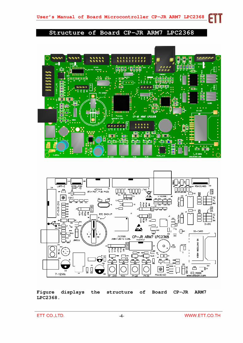
Structure of Board CP-JR ARM7 LPC2368
Figure displays the structure of Board CP-JR ARM7 LPC2368.
User’s Manual of Board Microcontroller CP-JR ARM7 LPC2368
ETT CO.,LTD. -5- WWW.ETT.CO.TH
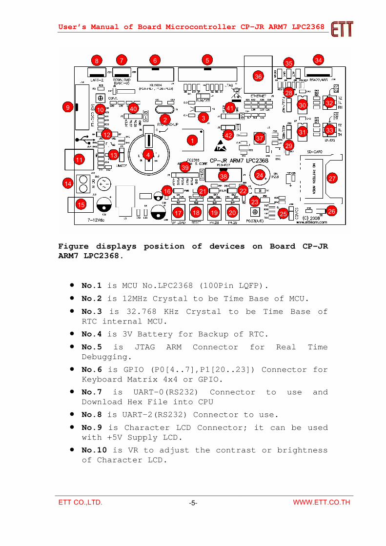
Figure displays position of devices on Board CP-JR ARM7 LPC2368.
• No.1 is MCU No.LPC2368 (100Pin LQFP). • No.2 is 12MHz Crystal to be Time Base of MCU. • No.3 is 32.768 KHz Crystal to be Time Base of
RTC internal MCU. • No.4 is 3V Battery for Backup of RTC. • No.5 is JTAG ARM Connector for Real Time
Debugging. • No.6 is GPIO (P0[4..7],P1[20..23]) Connector for
Keyboard Matrix 4x4 or GPIO. • No.7 is UART-0(RS232) Connector to use and
Download Hex File into CPU • No.8 is UART-2(RS232) Connector to use. • No.9 is Character LCD Connector; it can be used
with +5V Supply LCD. • No.10 is VR to adjust the contrast or brightness
of Character LCD.
1
5678
9
11
14
15
36
439
38
34
28
2724
17 18 19 2023
403
412
21 2216
12
13
25 26
29
30
31
32
33
35
3742
10
User’s Manual of Board Microcontroller CP-JR ARM7 LPC2368
ETT CO.,LTD. -6- WWW.ETT.CO.TH
• No.11 is USB Connector to connect with USB Hub version 2.0.
• No.12 is LED to display status of operation and the USB connection.
• No.13 is Jumper to select Mode of USB Connection.
• No.14 and No.15 is Power Supply Connector of board; it can be used with 7-12V AC/DC.
• No.16 is LED to display status of Power +VDD (+3V3).
• No.17 is SW1 that is ISP LOAD or P2.10/EINT0. • No.18 is SW2 or RESET Switch. • No.19 and No.20 is SW3 and SW4 to test Logic
Input of P4[28] and P4[29]. • No.21 and No.22 is LED to test Logic Output of
P3[25] and P3[26]. • No.23 is VR to adjust 0-3V3 Voltage for testing
A/D (P0[23]/AD0[0]). • No.24 is Mini Speaker to generate various
frequencies. • No.25 is Jumper to select Power Supply for
SD/MMC Memory Card. • No.26 is LED to display status of Power Supply
of SD/MMC Memory Card. • No.27 is socket to insert Memory Card; it can be
used with both SD Memory Card and MMC Memory Card.
• No.28 and No.29 is Jumper to select operation of RS422/485.
• No.30 is IC Line Driver of RS422 Receive; it can be used with 75176 or MAX3088.
• NO.31 is IC Line Driver of RS422 Transmit and RS485 Transceiver; it can be used with No.75176 or MAX3088.
• No.32 and No.33 is Jumper to set Enable/Disable Fail-Save Resistor and Terminate Resistor of RS422 Receive, RS455 Transmit (RS485 Transceiver).
User’s Manual of Board Microcontroller CP-JR ARM7 LPC2368
ETT CO.,LTD. -7- WWW.ETT.CO.TH
• No.34 is RS422/485 Connector. • No.35 is LED to display status of Ethernet LAN. • No.36 is RJ45 Ethernet LAN Connector. • No.37 is IC Physical Ethernet Driver No.DP83848. • Connector 38 is GPIO (P2[0..7] Connector for
Full-Duplex UART1 or GPIO. • No.39 is SPI0-Bus Connector or GPIO P0[15..18]. • No.40 is I2C-Bus Connector or GPIO P0[27..28]. • No.41 is A/D Connector or GPIO P0[24..25]. • No.42 is D/A Connector or GPIO P0.26.
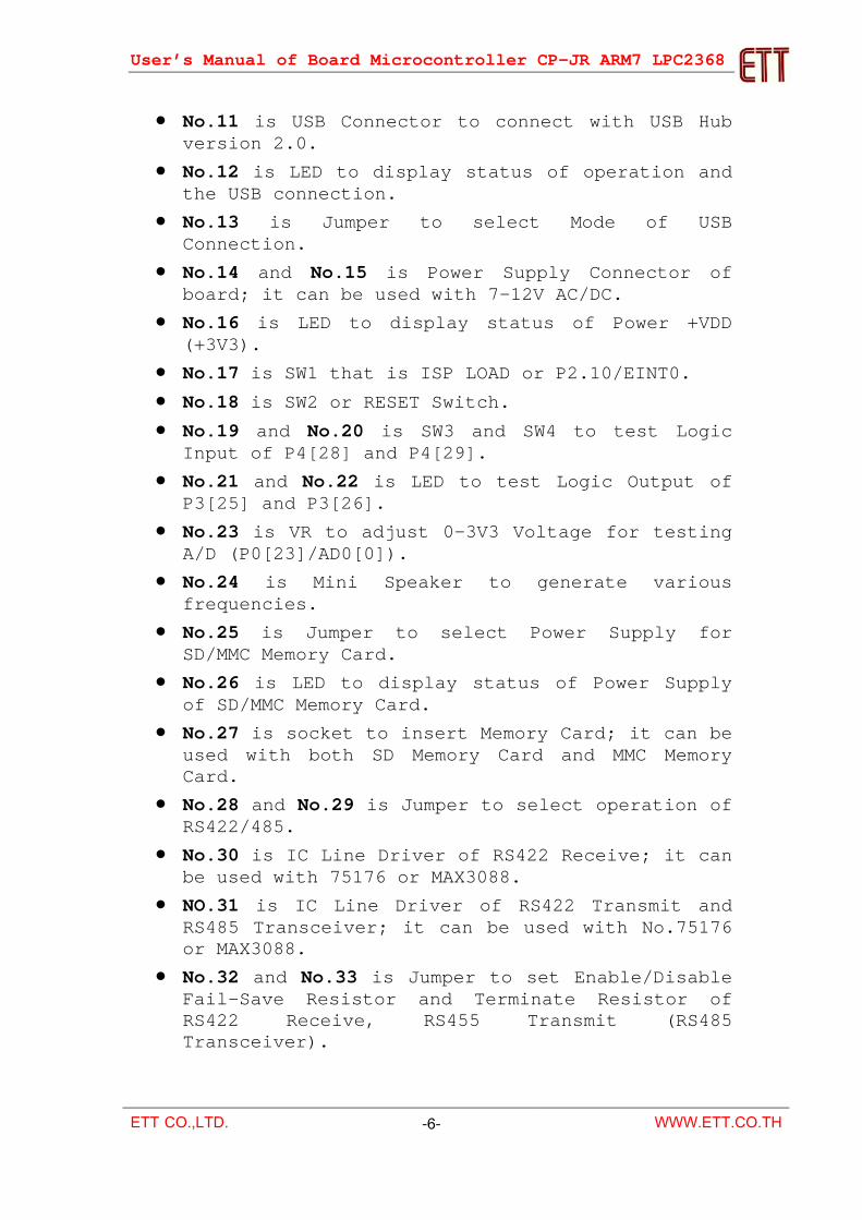
Applications of LED Display LED Display circuit of Board will be connected as Sink Current type and it is used with +3.3V Power Supply. In this case, it runs with Logic “0” (0V) and stops running with Logic “1” (+3.3V). It is controlled by 2 GPIOs that are P3[25] and P3[26]. This circuit is used to test operation of Output.
R53560
+3V3
R54560
+3V3
P3.25 P3.26
D12P3.25
D13P3.26
If we want to use this function, we must set function of P3[25] and P3[26] to be Output Port first and then control the desired Logic for P3[25] and P3[26] as example below.
User’s Manual of Board Microcontroller CP-JR ARM7 LPC2368
ETT CO.,LTD. -8- WWW.ETT.CO.TH
// Config Pin GPIO = P3[26:25] Drive LED PINSEL7 &= 0xFFC3FFFF; // Config P3[26:25] = GPIO Function PINMODE7 &= 0xFFC3FFFF; // Enable Pull-Up on P3[26:25] FIO3DIR |= 0x02000000; // Set P3[25] = Output FIO3DIR |= 0x04000000; // Set P3[26] = Output FIO3CLR = 0x02000000; // LED(P3[25]) = ON FIO3CLR = 0x04000000; // LED(P3[26]) = ON FIO3SET = 0x02000000; // LED(P3[25]) = OFF FIO3SET = 0x04000000; // LED(P3[26]) = OFF
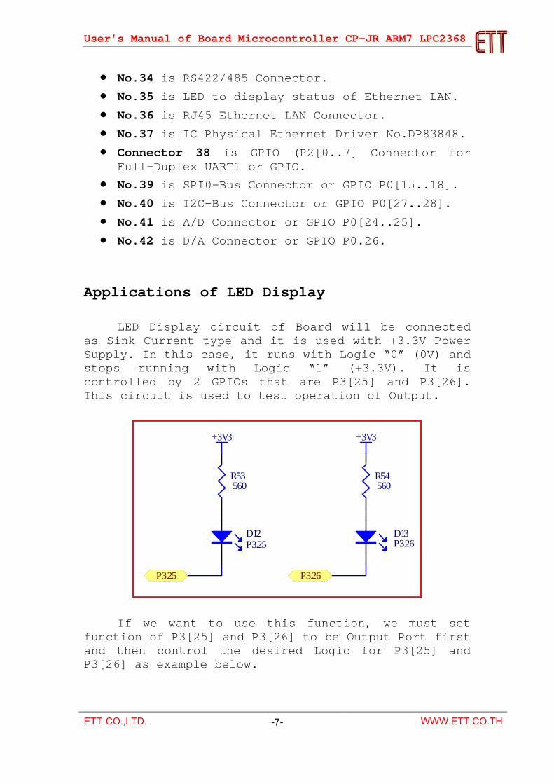
Application of Push Button Switch This circuit uses Push Button Switch Circuit with Pull-Up circuit; in this case, it can be used with +3.3V Power Supply. If Switch is not pressed, its status is Logic “1”; on the other hand, if Switch is pressed, its status is Logic “0”. It is used to test operation of Input Logic; moreover, this circuit has 3 sets as follows;
• SW1 (P2[10]) for ISP Download and test Input or Interrupt(EINT0)
• SW3 (P4[28]) to test Logic Input • SW4 (P4[29]) to test Logic Input
SW3P4.28
R5610K
R58
1K
+3V3
SW4P4.29
R5710K
R59
1K
+3V3
P4.28 P4.29SW1
ISP LOAD
C15100n
R31K
R122K
+3V3
P2.10

User’s Manual of Board Microcontroller CP-JR ARM7 LPC2368
ETT CO.,LTD. -9- WWW.ETT.CO.TH
Applications of Voltage Divider (0-3V3)
The Voltage Divider Circuit uses Adjustable Variable Resistor (VR) and it can be used with +3.3V Power Supply. In this case, its Output is voltage in the rage of 0V to +3.3V depend on the adjusting VR. The Output will be inputted into Pin P0[23] to generate Input voltage for testing operation of A/D (P0[23]) circuit.
P110K
R55
470
+3V3
P0.23
Application of Sound Generator
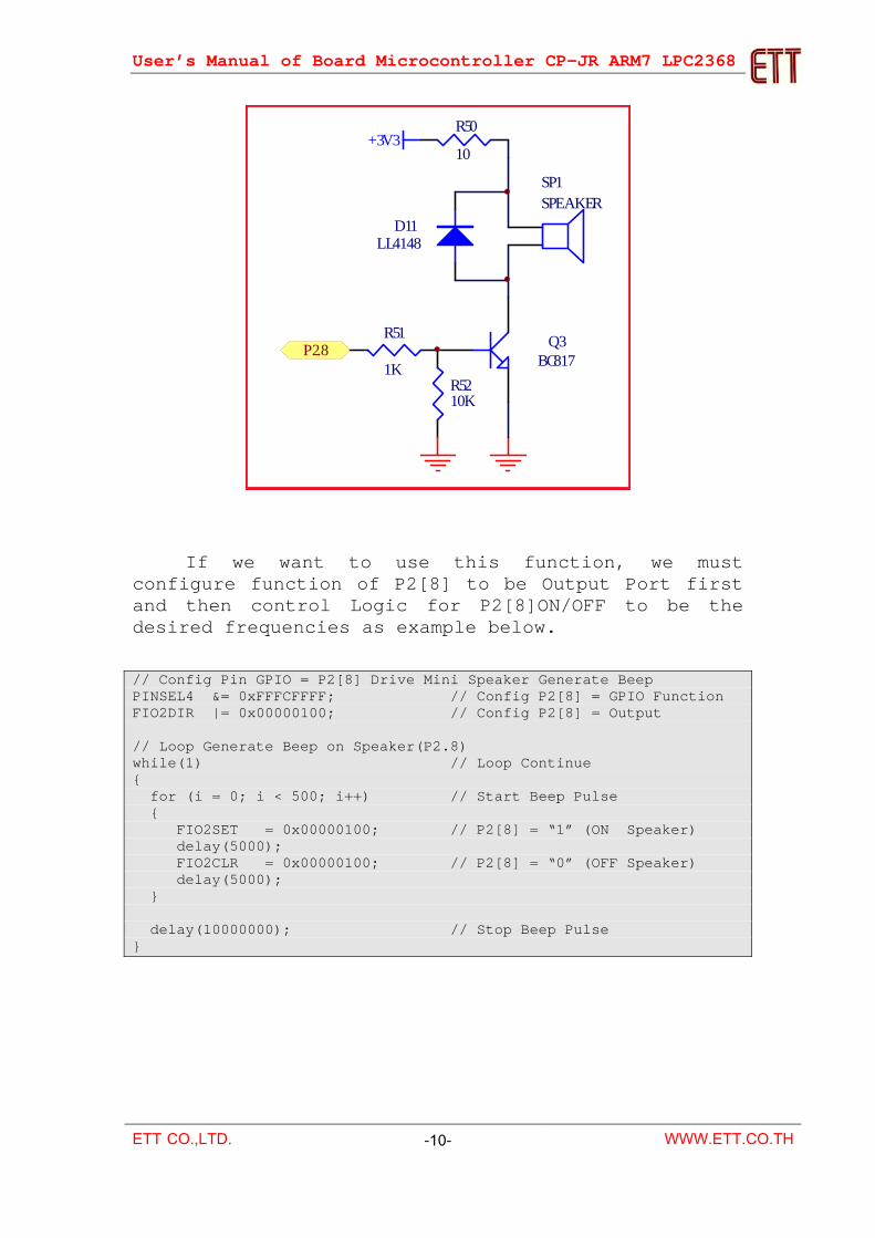
Sound Generator Circuit uses Mini Speaker with NPN Transistor circuit to drive current into speaker and can be used with +3.3V Power Supply. In this case, it runs with Logic “1” and stop running with Logic “0”. If we want to use this function, we must send signal Logic that is various frequencies into speaker to generate various frequency ranges as desired; in this case, it is controlled by P2[8].
User’s Manual of Board Microcontroller CP-JR ARM7 LPC2368
ETT CO.,LTD. -10- WWW.ETT.CO.TH
+3V3
P2.8 Q3BC817
SP1SPEAKER
D11LL4148
R51
1KR5210K
R50
10
If we want to use this function, we must
configure function of P2[8] to be Output Port first and then control Logic for P2[8]ON/OFF to be the desired frequencies as example below. // Config Pin GPIO = P2[8] Drive Mini Speaker Generate Beep PINSEL4 &= 0xFFFCFFFF; // Config P2[8] = GPIO Function FIO2DIR |= 0x00000100; // Config P2[8] = Output // Loop Generate Beep on Speaker(P2.8) while(1) // Loop Continue { for (i = 0; i < 500; i++) // Start Beep Pulse { FIO2SET = 0x00000100; // P2[8] = “1” (ON Speaker) delay(5000); FIO2CLR = 0x00000100; // P2[8] = “0” (OFF Speaker) delay(5000); } delay(10000000); // Stop Beep Pulse }
User’s Manual of Board Microcontroller CP-JR ARM7 LPC2368
ETT CO.,LTD. -11- WWW.ETT.CO.TH
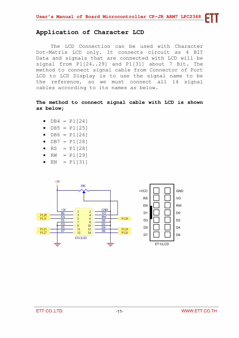
Application of Character LCD
The LCD Connection can be used with Character Dot-Matrix LCD only. It connects circuit as 4 BIT Data and signals that are connected with LCD will be signal from P1[24..29] and P1[31] about 7 Bit. The method to connect signal cable from Connector of Port LCD to LCD Display is to use the signal name to be the reference, so we must connect all 14 signal cables according to its names as below. The method to connect signal cable with LCD is shown as below;
• DB4 = P1[24] • DB5 = P1[25] • DB6 = P1[26] • DB7 = P1[28] • RS = P1[28] • RW = P1[29] • EN = P1[31]
1 23 45 67 89 1011 1213 14
ET-CLCD
P1.29
P1.24P1.26
P1.28P1.31
P1.25P1.27
GNDVORWD0D2D4D6
+5VRSEND1D3D5D7
10K+5V
END1D3D5
RWD0D2D4
VORSGND+VCC
D7 D6
ET-CLCD
User’s Manual of Board Microcontroller CP-JR ARM7 LPC2368
ETT CO.,LTD. -12- WWW.ETT.CO.TH
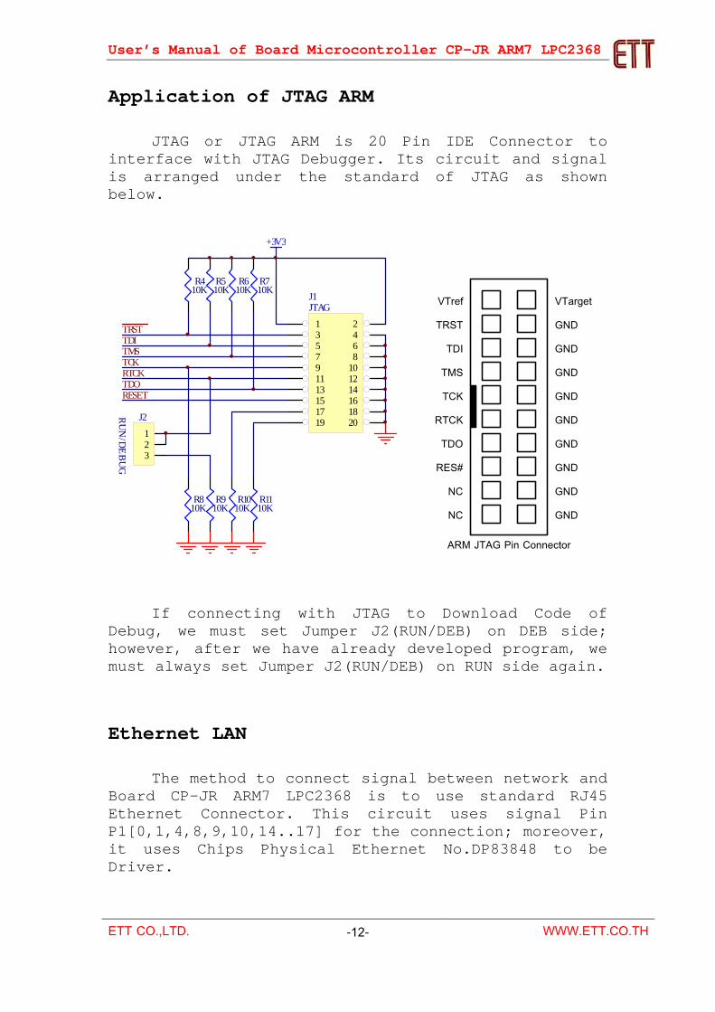
Application of JTAG ARM
JTAG or JTAG ARM is 20 Pin IDE Connector to interface with JTAG Debugger. Its circuit and signal is arranged under the standard of JTAG as shown below.
1 23 45 67 89 1011 1213 1415 161719
1820
J1JTAG
R410K
R510K
R610K
R710K
R1110K
R1010K
R910K
R810K
+3V3
TRSTTDITMSTCKRTCKTDORESET
123
J2RU
N/D
EB
UG
TRSTTDI
TMSTCK
GNDGNDGNDGND
VTref
ARM JTAG Pin Connector
GNDGNDGNDGNDGND
RTCKTDO
RES#NCNC
VTarget
If connecting with JTAG to Download Code of Debug, we must set Jumper J2(RUN/DEB) on DEB side; however, after we have already developed program, we must always set Jumper J2(RUN/DEB) on RUN side again. Ethernet LAN The method to connect signal between network and Board CP-JR ARM7 LPC2368 is to use standard RJ45 Ethernet Connector. This circuit uses signal Pin P1[0,1,4,8,9,10,14..17] for the connection; moreover, it uses Chips Physical Ethernet No.DP83848 to be Driver.
User’s Manual of Board Microcontroller CP-JR ARM7 LPC2368
ETT CO.,LTD. -13- WWW.ETT.CO.TH
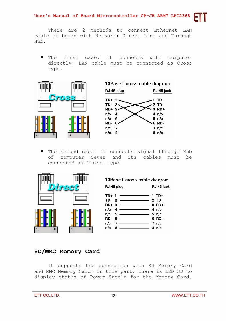
There are 2 methods to connect Ethernet LAN cable of board with Network; Direct Line and Through Hub.
• The first case; it connects with computer directly; LAN cable must be connected as Cross type.
• The second case; it connects signal through Hub
of computer Sever and its cables must be connected as Direct type.
SD/MMC Memory Card It supports the connection with SD Memory Card and MMC Memory Card; in this part, there is LED SD to display status of Power Supply for the Memory Card.
User’s Manual of Board Microcontroller CP-JR ARM7 LPC2368
ETT CO.,LTD. -14- WWW.ETT.CO.TH
Power Supply of Memory Card can be selected by Jumper J26(SD/VDD); so we can select to use Power Supply either from +VDD of Board or from the control of signal Pin MCIPWR. Normally, we set Jumper J26(SD/VDD) on SD side to use Power Supply of Memory Card from the control of MCIPWR. All circuits to connect with Memory Card uses signal pins from MCU as follows;
• MCIDAT0 uses P0.22. • MCIDAT1 uses P2.11. • MCIDAT2 uses P2.12. • MCIDAT3 uses P2.13. • MCICMD uses P0.20. • MCICLK uses P0.19. • MCIPWR uses P0.21.
• CD uses P0.8 (GPIO) to test Insert Memory Card.
• WP uses P0.9 (GPIO) to test the setting of Write Protect of Memory Card.
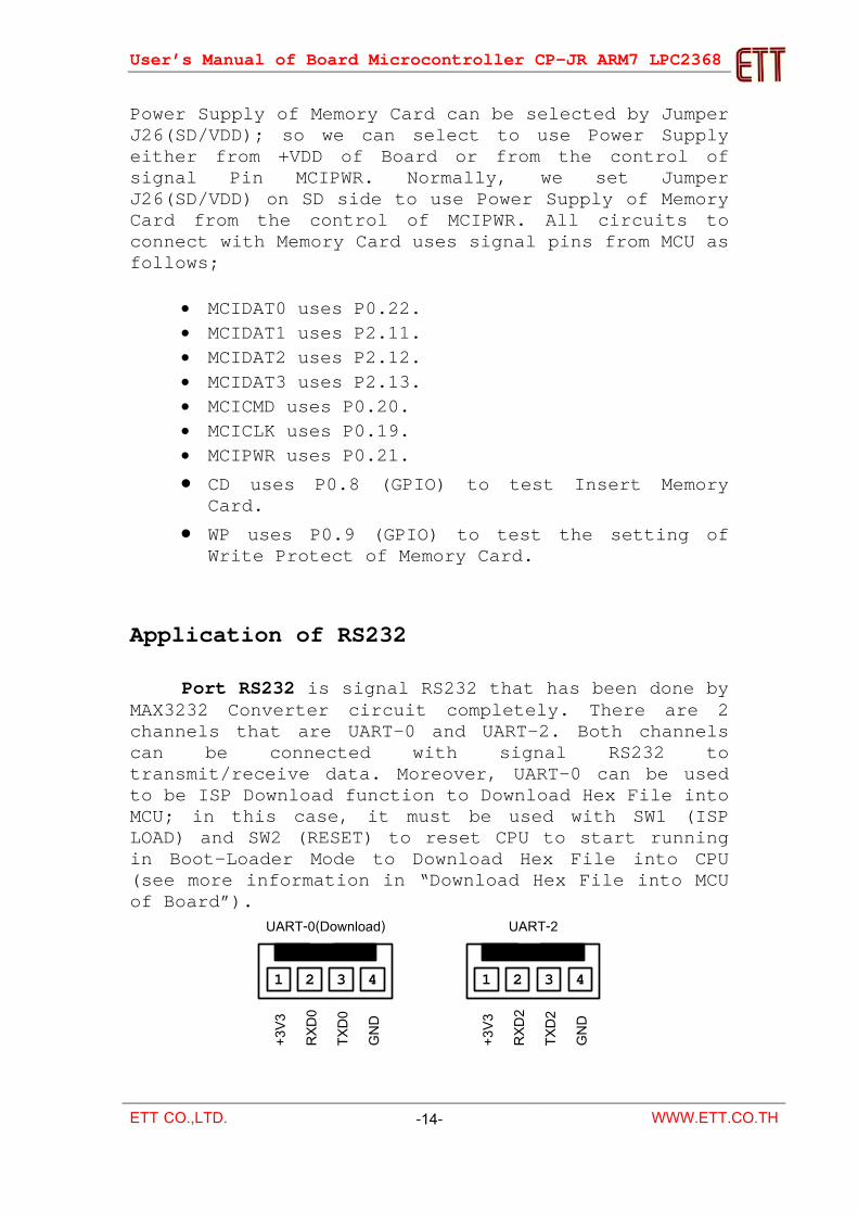
Application of RS232
Port RS232 is signal RS232 that has been done by MAX3232 Converter circuit completely. There are 2 channels that are UART-0 and UART-2. Both channels can be connected with signal RS232 to transmit/receive data. Moreover, UART-0 can be used to be ISP Download function to Download Hex File into MCU; in this case, it must be used with SW1 (ISP LOAD) and SW2 (RESET) to reset CPU to start running in Boot-Loader Mode to Download Hex File into CPU (see more information in “Download Hex File into MCU of Board”).
2 41 3
+3V3
RXD0
TXD0
GND
UART-0(Download)
2 41 3
+3V3
RXD2
TXD2
GND
UART-2
User’s Manual of Board Microcontroller CP-JR ARM7 LPC2368
ETT CO.,LTD. -15- WWW.ETT.CO.TH
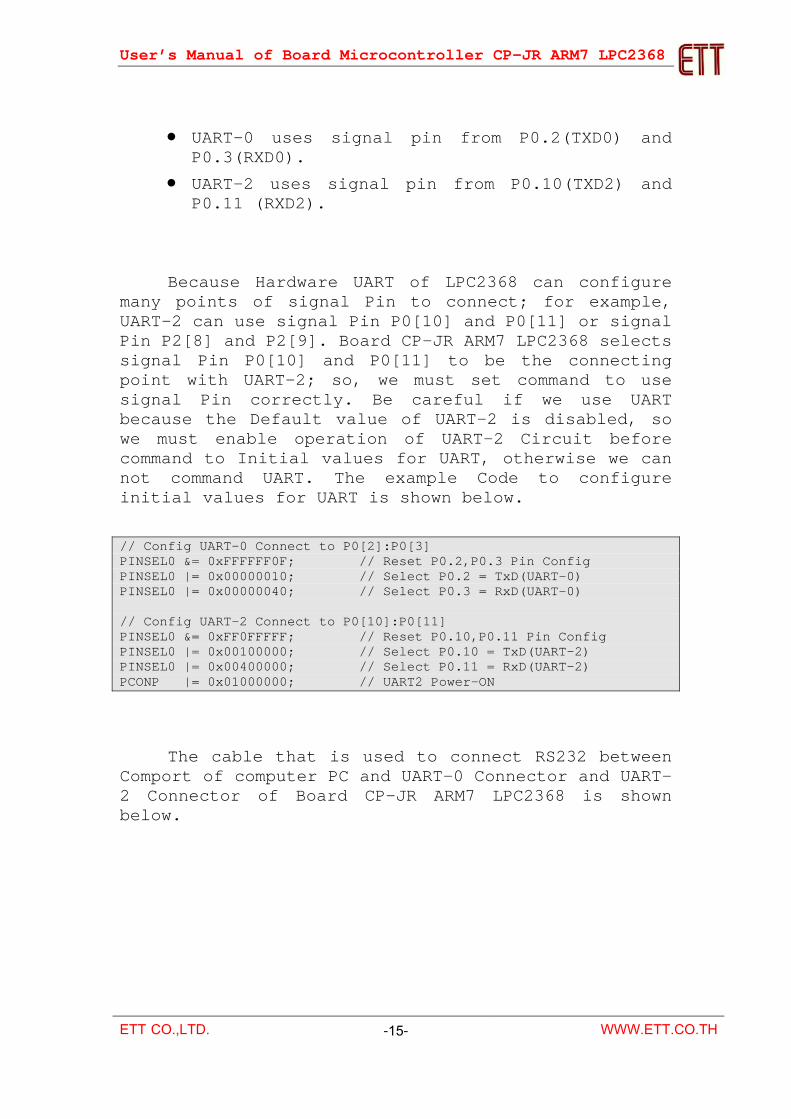
• UART-0 uses signal pin from P0.2(TXD0) and
P0.3(RXD0). • UART-2 uses signal pin from P0.10(TXD2) and
P0.11 (RXD2).
Because Hardware UART of LPC2368 can configure many points of signal Pin to connect; for example, UART-2 can use signal Pin P0[10] and P0[11] or signal Pin P2[8] and P2[9]. Board CP-JR ARM7 LPC2368 selects signal Pin P0[10] and P0[11] to be the connecting point with UART-2; so, we must set command to use signal Pin correctly. Be careful if we use UART because the Default value of UART-2 is disabled, so we must enable operation of UART-2 Circuit before command to Initial values for UART, otherwise we can not command UART. The example Code to configure initial values for UART is shown below.
// Config UART-0 Connect to P0[2]:P0[3] PINSEL0 &= 0xFFFFFF0F; // Reset P0.2,P0.3 Pin Config PINSEL0 |= 0x00000010; // Select P0.2 = TxD(UART-0) PINSEL0 |= 0x00000040; // Select P0.3 = RxD(UART-0) // Config UART-2 Connect to P0[10]:P0[11] PINSEL0 &= 0xFF0FFFFF; // Reset P0.10,P0.11 Pin Config PINSEL0 |= 0x00100000; // Select P0.10 = TxD(UART-2) PINSEL0 |= 0x00400000; // Select P0.11 = RxD(UART-2) PCONP |= 0x01000000; // UART2 Power-ON
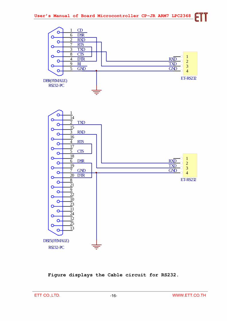
The cable that is used to connect RS232 between
Comport of computer PC and UART-0 Connector and UART-2 Connector of Board CP-JR ARM7 LPC2368 is shown below.
User’s Manual of Board Microcontroller CP-JR ARM7 LPC2368
ETT CO.,LTD. -16- WWW.ETT.CO.TH
162738495
DB9(FEMALE)
1234
ET-RS232
RXDTXDGND
RXDRTS
DSR
TXDCTSDTR
GND
CD
RI
RS232-PC
1234
ET-RS232
11421531641751861972082192210231124122513
DB25(FEMALE)
TXD
RXD
RTS
CTS
DSR
GNDDTR
RXDTXDGND
RS232-PC
Figure displays the Cable circuit for RS232.
User’s Manual of Board Microcontroller CP-JR ARM7 LPC2368
ETT CO.,LTD. -17- WWW.ETT.CO.TH
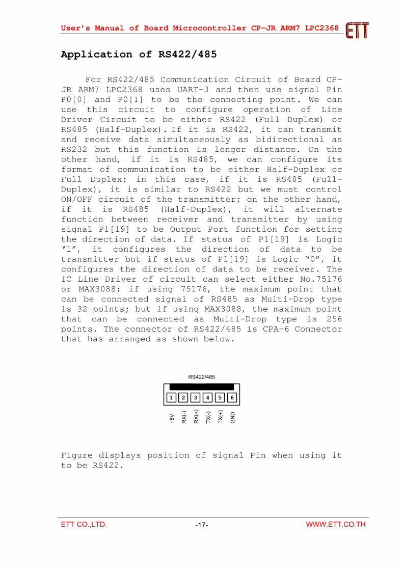
Application of RS422/485
For RS422/485 Communication Circuit of Board CP-JR ARM7 LPC2368 uses UART-3 and then use signal Pin P0[0] and P0[1] to be the connecting point. We can use this circuit to configure operation of Line Driver Circuit to be either RS422 (Full Duplex) or RS485 (Half-Duplex). If it is RS422, it can transmit and receive data simultaneously as bidirectional as RS232 but this function is longer distance. On the other hand, if it is RS485, we can configure its format of communication to be either Half-Duplex or Full Duplex; in this case, if it is RS485 (Full-Duplex), it is similar to RS422 but we must control ON/OFF circuit of the transmitter; on the other hand, if it is RS485 (Half-Duplex), it will alternate function between receiver and transmitter by using signal P1[19] to be Output Port function for setting the direction of data. If status of P1[19] is Logic “1”, it configures the direction of data to be transmitter but if status of P1[19] is Logic “0”, it configures the direction of data to be receiver. The IC Line Driver of circuit can select either No.75176 or MAX3088; if using 75176, the maximum point that can be connected signal of RS485 as Multi-Drop type is 32 points; but if using MAX3088, the maximum point that can be connected as Multi-Drop type is 256 points. The connector of RS422/485 is CPA-6 Connector that has arranged as shown below.
1 3 52 4 6
RX(-)
GND
RX(+)
TX(-)
TX(+)
+5V
RS422/485
Figure displays position of signal Pin when using it to be RS422.
User’s Manual of Board Microcontroller CP-JR ARM7 LPC2368
ETT CO.,LTD. -18- WWW.ETT.CO.TH
1 3 52 4 6
RX(-)
GND
RX(+)
TX(-)
TX(+)
+5V
RS422/485
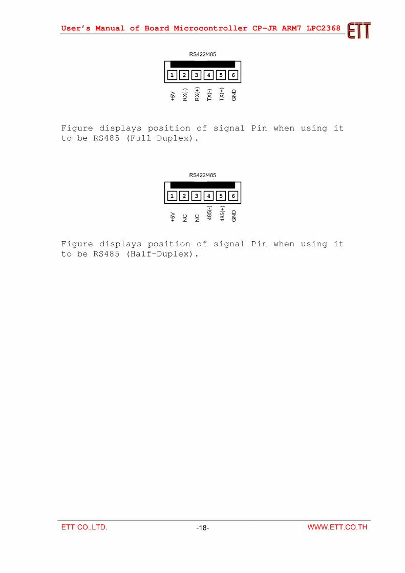
Figure displays position of signal Pin when using it to be RS485 (Full-Duplex).
1 3 52 4 6
NC GND
NC 485(-
)
485(+
)
+5V
RS422/485
Figure displays position of signal Pin when using it to be RS485 (Half-Duplex).
User’s Manual of Board Microcontroller CP-JR ARM7 LPC2368
ETT CO.,LTD. -19- WWW.ETT.CO.TH
A 6
GND 5
R1
RE2
DE3
D4
VCC 8
B 7
U675176
A 6
GND 5
R1
RE2
DE3
D4
VCC 8
B 7
U775176
123456
J18RS422/485
R601K
R611K
R62120
R631K
R641K
R65120
C42
100n
C43
100n
+5V
+5V
+5V
+5V
+5V
+5V
RX-RX+TX-TX+
RXD3
TXD3
P1[19]
1 2 3 J19
FULL/HALF
1 2 3 J20
422/485
123
J15RL
123
J16
RH
123
J17
RZ
123
J21TH
123
J22
TL
123
J23
TZ
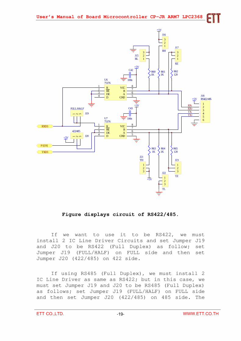
Figure displays circuit of RS422/485.
If we want to use it to be RS422, we must install 2 IC Line Driver Circuits and set Jumper J19 and J20 to be RS422 (Full Duplex) as follow; set Jumper J19 (FULL/HALF) on FULL side and then set Jumper J20 (422/485) on 422 side.
If using RS485 (Full Duplex), we must install 2 IC Line Driver as same as RS422; but in this case, we must set Jumper J19 and J20 to be RS485 (Full Duplex) as follows; set Jumper J19 (FULL/HALF) on FULL side and then set Jumper J20 (422/485) on 485 side. The
User’s Manual of Board Microcontroller CP-JR ARM7 LPC2368
ETT CO.,LTD. -20- WWW.ETT.CO.TH
operation is similar to RS422 because it can simultaneously transmit and receive data as bidirectional type like RS422 but it can be connected as Multi-Drop type. The circuit can receive data all the time through IC Line Driver of U6 and IC Line Driver U7 will transmit data. In this case, it can control ON/OFF operation of transmitting data by signal from P1[19]; if status of P1[19] is Logic “1”, it enables operation of transmitting data but if status of P1[19] is Logic “0”, it disables operation of transmitting data. When the operation of transmitting data is disabled, its status is similar to removing cable of the transmitter from circuit, so signal on the transmitter does not crash data of other devices. We must write program to control all devices to transmit only one data into a line once.
If using RS485 (Half-Duplex), we must install only one IC Line Driver at position U7; in this case, we must set Jumper J19 and J20 to be RS485 (Half Duplex) as follows; set Jumper J19 (FULL/HALF) on HALF side and then set Jumper J20 (422/485) on 485 side. Moreover, we must interface cable of CPA-6(J18) Connector at the position TX(-) and TX(+); in this case, function of TX(-) is RS485(-) and function of TX(+) is RS485(+). Direction and function of this signal RS485 depends on status Logic of P1[19] that is Pin Output Port and its function is Direction Control.
The method to set Jumper of Fail-Save Resistor and Terminate Resistor is describes as follows; if Board is generally installed in the beginning position and destination of these Jumper Cables, we must enable and then set Jumper(EN/DIS) of RZ, RL, RH, TZ, TL and TH on EN side or always Enable. The Fail-Safe Resistor (RL, RH, TL and TH) makes status Logic in the signal cable is in the correct IDLE status while not receiving and transmitting any data. For the Terminate Resistor (RZ and TZ) will compensate the resistance or Impedance that is occurred in the line if it is very long line. Code for writing program to configure operation of UART-3 of RS422/485, we must use P0[0] and P0[1]
User’s Manual of Board Microcontroller CP-JR ARM7 LPC2368
ETT CO.,LTD. -21- WWW.ETT.CO.TH
to be the connecting Pin and then use P1[19] to control the direction of receiving and transmitting data of RS485. Be careful, the Default value of the UART-3 Circuit in LPC2368 is normally disabled; so, if we want to enable operation of this circuit, we must not forget to write command to enable operation of UART-3 before setting configurations into circuit. The method to enable operation of UART-3 is to be controlled by Bit in Register PCONP as example below.
// Config UART-3(RS422/485) Connect to P0[0]:P0[1] PINSEL0 &= 0xFFFFFFF0; // Reset P0.0,P0.1 Pin Config PINSEL0 |= 0x00000002; // Select P0.0 = TxD(UART3) PINSEL0 |= 0x00000008; // Select P0.1 = RxD(UART3) PCONP |= 0x02000000; // UART3 Power-ON // Config P1.19 = Output Control Direction RS485 // P1.19 = "0" = Received RS485 // P1.19 = "1" = Transmit RS485 PINSEL3 &= 0xFFFF3FFF; // P1.19 = GPIO IODIR1 = 0x00080000; // Pin Control Direction RS485 = Output // Select Direction RS485 = Receive IOCLR1 = 0x00080000; // RS485 Direction = 0 (Receive) // Select Direction RS485 = Transmit IOSET1 = 0x00080000; // RS485 Direction = 1 (Transmit)
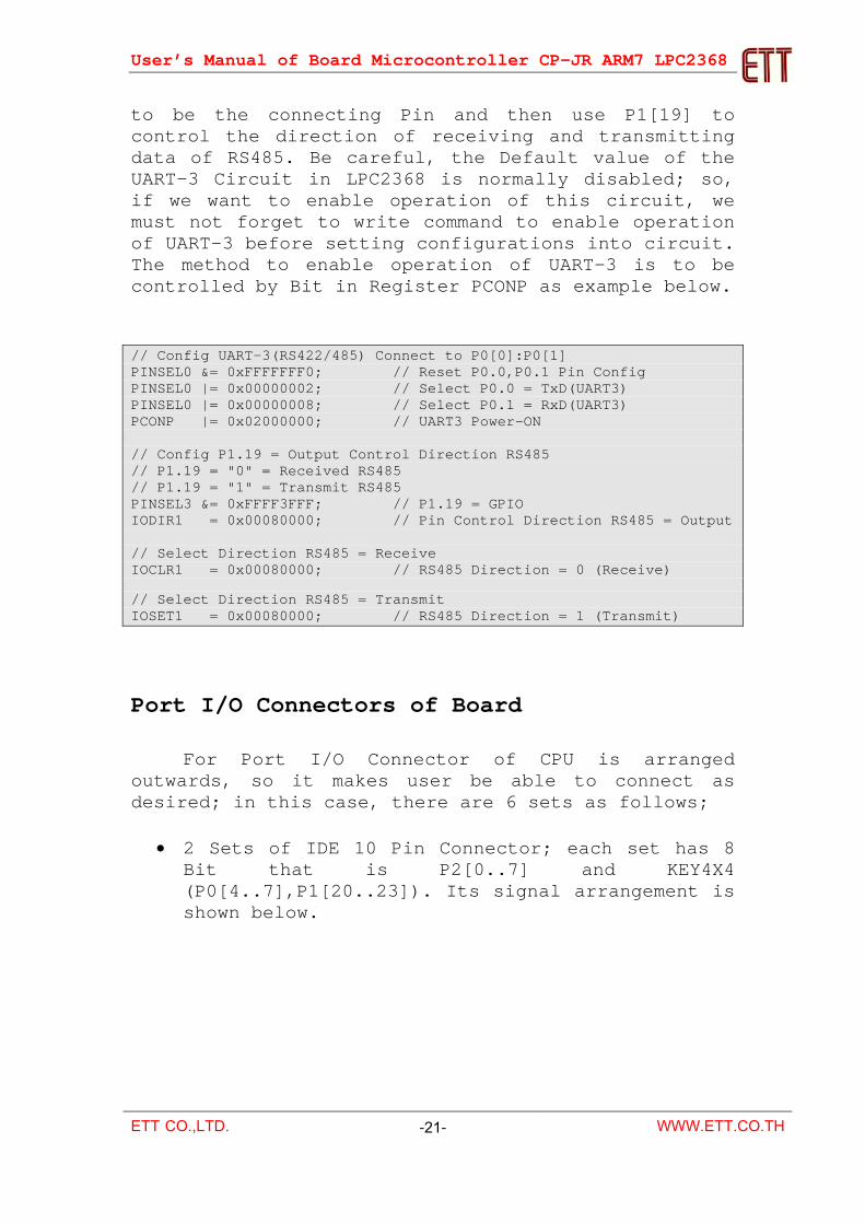
Port I/O Connectors of Board For Port I/O Connector of CPU is arranged outwards, so it makes user be able to connect as desired; in this case, there are 6 sets as follows;
• 2 Sets of IDE 10 Pin Connector; each set has 8 Bit that is P2[0..7] and KEY4X4 (P0[4..7],P1[20..23]). Its signal arrangement is shown below.
User’s Manual of Board Microcontroller CP-JR ARM7 LPC2368
ETT CO.,LTD. -22- WWW.ETT.CO.TH
P2.2P2.4P2.6+3V3
P2.3P2.5P2.7GND
P2.1P2.0
P2[0..7]
P0.6P1.20P1.22+3V3
P0.7P1.21P1.23GND
P0.5P0.4
P0[4..7],P1[20..23]
• SPI-0 Connector is 1x6 Header that is connecting
point P0[15..18] for using it to be general GPIO function or SPI Bus function as desired.
o P0.15 = SCK/SCK0 o P0.16 = SSEL/SSEL0 o P0.17 = MISO/MISO0 o P0.18 = MOSI/MOSI0
• I2C-0 Connector is 1x4 Header that is connecting point P0[27..28] for using it to be general GPIO function or I2C Bus function as desired.
o P0.27 = SDA0 o P0.28 = SCL0
• A/D Connector is 1x4 Header that is connecting point P0[24..25] for using it to be general GPIO function or A/D function as desired.
o P0.24 = AD0.1 o P0.25 = AD0.2
• D/A Connector is 1x3 Header that is connecting point P0[26] for using it to be general GPIO function or D/A(Aout) function as desired.
o P0.26 = AOUT or D/A Power Supply Circuit
Power Supply Circuit can be used with 7-12V AC/DC; in this case, we can interface Power Supply into board at the connecting point that is Terminal or Jack-DC as desired. This connecting Power Supply
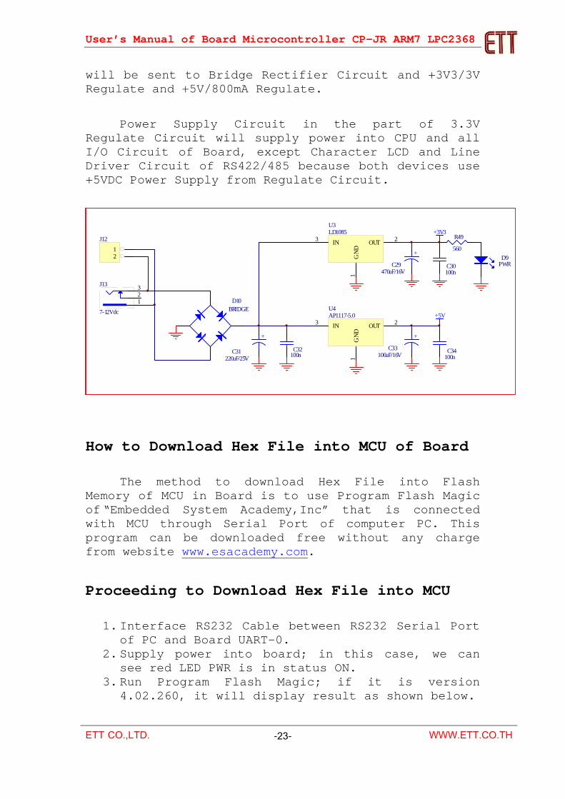
User’s Manual of Board Microcontroller CP-JR ARM7 LPC2368
ETT CO.,LTD. -23- WWW.ETT.CO.TH
will be sent to Bridge Rectifier Circuit and +3V3/3V Regulate and +5V/800mA Regulate.
Power Supply Circuit in the part of 3.3V
Regulate Circuit will supply power into CPU and all I/O Circuit of Board, except Character LCD and Line Driver Circuit of RS422/485 because both devices use +5VDC Power Supply from Regulate Circuit.
C32100n
C34100n
+5V
C30100n
+3V3R49
560D9
PWR
123J13
7-12Vdc
+
C29470uF/16V
+
C33100uF/16V
+
C31220uF/25V
12
J12
IN3
GN
D1
OUT 2
U4AP1117-5.0
D10BRIDGE
IN3
GN
D1
OUT 2
U3LD1085
How to Download Hex File into MCU of Board
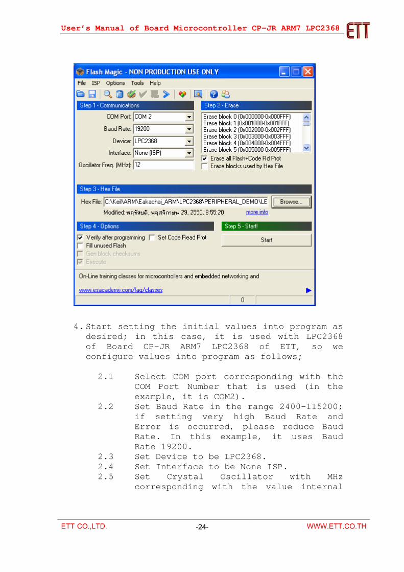
The method to download Hex File into Flash Memory of MCU in Board is to use Program Flash Magic of “Embedded System Academy,Inc” that is connected with MCU through Serial Port of computer PC. This program can be downloaded free without any charge from website www.esacademy.com.
Proceeding to Download Hex File into MCU
1. Interface RS232 Cable between RS232 Serial Port of PC and Board UART-0.
2. Supply power into board; in this case, we can see red LED PWR is in status ON.
3. Run Program Flash Magic; if it is version 4.02.260, it will display result as shown below.
User’s Manual of Board Microcontroller CP-JR ARM7 LPC2368
ETT CO.,LTD. -24- WWW.ETT.CO.TH
4. Start setting the initial values into program as
desired; in this case, it is used with LPC2368 of Board CP-JR ARM7 LPC2368 of ETT, so we configure values into program as follows;
2.1 Select COM port corresponding with the
COM Port Number that is used (in the example, it is COM2).
2.2 Set Baud Rate in the range 2400-115200; if setting very high Baud Rate and Error is occurred, please reduce Baud Rate. In this example, it uses Baud Rate 19200.
2.3 Set Device to be LPC2368. 2.4 Set Interface to be None ISP. 2.5 Set Crystal Oscillator with MHz
corresponding with the value internal
User’s Manual of Board Microcontroller CP-JR ARM7 LPC2368
ETT CO.,LTD. -25- WWW.ETT.CO.TH
Board. In this case, it is 12.000MHz, so we must set to be 12.
2.6 Press ISP LOAD Switch and RESET Switch on Board “CP-JR ARM7 LPC2368” to reset MCU to run in Boot Loader following the processes; Press ISP LOAD Switch and hold Press RESET Switch while ISP LOAD Switch is being held.
Remove RESET Switch but ISP LOAD Switch is being held.
Lastly, remove ISP LOAD Switch. 5. Select format of erasing data to be “Erase all
Flash + Code Rd Prot”. 6. Set Option to be “Verify after programming”. 7. Click “Browse” to select HEX File for
downloading. 8. Click “Start”, Program Flash Magic will start
downloading data into MCU instantly. In this case, we can see the status operation at Status Bar and we must wait for the operation until it is completely.
9. When the operation of program is complete, press RESET Switch on Board and MCU will start running follow the downloaded program instantly.

1 2 3 4
A
B
C
D
4321
D
C
B
A Title
Number RevisionSize
A4
Date: 31-Jan-2008 Sheet of File: D:\My Circuit\LPC2368.Ddb Drawn By:
P1.0/ENET-TXD095
P1.1/ENET-TXD194
P1.4/ENET-TX_EN93
P1.8/ENET-CRS92
P1.9/ENET-RXD091
P1.10/ENET-RXD190
P1.14/ENET-RX_ER89
P1.15/ENET-RX_CLK88
P1.16/ENET-MDC87
P1.17/ENET-MDIO86
P1.18/USB_UP_LED/PWM1.1/CAP1.032
P1.19/CAP1.133
P1.20/PWM1.2/SCK034
P1.21/PWM1.3/SSEL035
P1.22/MAT1.036
P1.23/PWM1.4/MISO037
P1.24/PWM1.5/MOSI038
P1.25/MAT1.139
P1.26/PWM1.6/CAP0.040
P1.27/CAP0.143
P1.28/PCAP1.0/MAT0.044
P1.29/PCAP1.1/MAT0.145
P1.30/USB_VBUS/AD0.421
P1.31/SCK1/AD0.520
P3.25/MAT0.0/PWM1.227
P3.26/MAT0.1/PWM1.326
P4.28/MAT2.0/TXD382
P4.29/MAT2.1/RXD385
VDDA10
VREFA12
DC-DC_3.3V_VDD113
DC-DC_3.3V_VDD242
DC-DC_3.3V_VDD384
VDD128
VDD254
VDD371
VDD496
VBAT19
VSS115
VSS231
VSS341
VSS455
VSS572
VSS697
VSS783
VSSA11
P0.0/RD1/TXD3/SDA1 46
P0.1/TD1/RXD3/SCL1 47
P0.2/TXD0 98
P0.3/RXD0 99
P0.4/I2SRX_CLK/RD2/CAP2.0 81
P0.5/I2SRX_WS/TD2/CAP2.1 80
P0.6/I2SRX_SDA/SSEL1/MAT2.0 79
P0.7/I2STX_CLK/SCK1/MAT2.1 78
P0.8/I2STX_WS/MISO1/MAT2.2 77
P0.9/I2STX_SDA/MOSI1/MAT2.3 76
P0.10/TXD2/SDA2/MAT3.0 48
P0.11/RXD2/SCL2//MAT3.1 49
P0.15/TXD1/SCK0/SCK 62
P0.16/RXD1/SSEL0/SSEL 63
P0.17/CTS1/MISO0/MISO 61
P0.18/DCD1/MOSI0/MOSI 60
P0.19/DSR1/MCICLK/SDA1 59
P0.20/DTR1/MCICMD/SCL1 58
P0.21/RI1/MCIPWR/RD1 57
P0.22/RTS1/MCIDAT0/TDI 56
P0.23/AD0.0/I2SRX_CLK/CAP3.0 9
P0.24/AD0.1/I2SRX_WS/CAP3.1 8
P0.25/AD0.2/I2SRX_SDA/TXD3 7
P0.26/AD0.3/AOUT/RXD3 6
P0.27/SDA0 25
P0.28/SCL0 24
P0.29/USB_D+ 29
P0.30/USB_D- 30
P2.0/PWM1.1/TXD1/TRACECLK 75
P2.1/PWM1.2/RXD1/PIPESTAT0 74
P2.2/PWM1.3/CTS1/PIPESTAT1 73
P2.3/PWM1.4/DCD1/PIPESTAT2 70
P2.4/PWM1.5/DSR1/TRACESYNC 69
P2.5/PWM1.6/DTR1/TRACEPKT0 68
P2.6/PCAP1.0/RI1/TRACEPKT1 67
P2.7/RD2/RTS1/TRACEPKT2 66
P2.8/TD2/TXD2/TRACEPKT3 65
P2.9/USB_CONNECT/RXD2/EXTINT0 64
P2.10/EINT0 53
P2.11/EINT1/MCIDAT1/I2STX_CLK 52
P2.12/EINT2/MCIDAT2/I2STX_WS 51
P2.13/EINT3/MCIDAT3/I2STX_SDA 50
TRST 4
TDI 2
TMS 3
TCK 5
RTCK 100
TDO 1
RSTOUT 14
RESET 17
RTCX1 16
RTCX2 18
XTA
L223
XTA
L122
U1LPC2368
Y1
12MHzC1122pF
C1222pF
Y2
32.768KHzC1322pF
C1422pF
SW2
RESET
SW1
ISP LOAD
C15100n
C16100n
R31K
R122K
R247K
+3V3
+3V3
1 23 45 67 89 1011 1213 1415 161719
1820
J1JTAG
R410K
R510K
R610K
R710K
R1110K
R1010K
R910K
R810K
+3V3
C7100n
C8100n
C9100n
C10100n
C6100n
C5100n
C4100n
C2100n
C3100n
+3V3
B13V
D2
PMEG4005ET
D1PMEG4005ET
+3V3
1 23 45 67 89 10
J4P2.0-P2.7
+3V3
1 23 45 67 89 10
J6KEY4X4
+3V3
123456
J3
SPI-0
+3V3
1234
J5
I2C-0
+3V3
ENET-TXD0ENET-TXD1ENET-TX_EN
ENET-CRSENET-RXD0ENET-RXD1ENET-RX_ER
ENET-RX_CLK
ENET-MDCENET-MDIO
USB_LEDDIR_485
P3.25P3.26
P4.28P4.29
LCD_DB4LCD_DB5LCD_DB6LCD_DB7LCD_RSLCD_RW
USB_VBUSLCD_EN
USB_D+USB_D-
RESET
RXD0TXD0RXD3TXD3
CDWP
TXD2RXD2
P2.8USB_CON
MCIDAT1MCIDAT2MCIDAT3
MCICLKMCICMDMCIPWRMCIDAT0P0.23
ISP_BOOT
ISP_BOOT
TRSTTDITMSTCKRTCKTDO
TRSTTDITMSTCKRTCKTDO
P2.0P2.1P2.2P2.3P2.4P2.5P2.6P2.7
P2.0P2.2P2.4P2.6
P2.1P2.3P2.5P2.7
P0.15
P0.16P0.17P0.18
P0.15P0.16P0.17P0.18
P0.27P0.28
P0.27P0.28
P0.24P0.25
P0.24P0.25
P0.26
P0.26
P0.4P0.6P1.20P1.22
P0.5P0.7P1.21P1.23
P0.4P0.5P0.6P0.7
P1.20P1.21P1.22P1.23 RESET
RESET
RESET
+
C110u
L1BEAD
+3V3
+3V3
123
J2RU
N/D
EBU
G
1234
J7
A/D
+3V3
123
J8
D/A
+3V3
CP-JR ARM7 LPC2368
1 4
1.0ETT CO.,LTD.(WWW.ETT.CO.TH)

1 2 3 4
A
B
C
D
4321
D
C
B
A Title
Number RevisionSize
A4
Date: 31-Jan-2008 Sheet of File: D:\My Circuit\LPC2368.Ddb Drawn By:
TK_C
LK1
TX_E
N2
TXD
_03
TXD
_14
TXD
_25
TXD
_3/S
NI_
MO
DE
6
PWR
_DO
WN
/INT
7
NC
8
NC
9
NC
10
NC
11
NC
12RD- 13RD+ 14AGND 15TD- 16TD+ 17PFBIN1 18AGND 19NC 20NC 21AVDD33 22PFBOUT 23RBIAS 24
25M
HZ_
OU
T25
LED
_AC
T/C
OL/
AN
_EN
26LE
D_S
PEED
/AN
127
LED
_LIN
K/A
N0
28R
ESET
_N29
MD
IO30
MD
C31
IOV
DD
3332
X2
33X
134
IOG
ND
35D
GN
D36
PFBIN237
RX_CLK38
RX_DV/MII_MODE39
CRS/CRS_DV/LED_CFG40
RX_ER/MDIX_EN41
COL/PHYAD042
RXD_0/PHYAD143
RXD_1/PHYAD244
RXD_2/PHYAD345
RXD_3/PHYAD446
IOGND47
IOVDD3348
U2DP83848
8
1
4
2
3
5
6
7
CHS GNDNC
1CT:1
TD+
TD-
CT
RD+
CT
RD-
TX+
TX-
RX+
RX-6
3
2
1
45
78
J9RJ45_PRJ-005
R23
10K+3V3
C22100n
R12
10K
+3V3
C18100n
4
2
3
1E/D
OUT
+3.3V
GNDOSC150MHz
C17
100n
+3V3
D3
100Mb
R14
680
R162K2+3V3
R154K87 1%
C19
100n
R182K2
R172K2
C21 100n R2050
R1950
R2150
R2250
C23100n
C25100n
C24100n
C26100n
+3V3 +3V3
+3V3
+3V3
+3V3
R13
2K2
+3V3
+3V3
PFBOUT
PFBOUT
LED
_AC
TLE
D_S
PEED
LED
_LIN
K
PFB
OU
T
50 M
Hz
D4
LINK
D5
ACT
R25
110
R27
110
R24
2K2
R26
2K2
+3V3
LED_LINK
LED_ACT
ENET
-TX
D0
ENET
-TX
D1
ENET
-TX
_EN
ENET-CRSENET-RX_ER
ENET-RXD0ENET-RXD1
ENET
-MD
CEN
ET-M
DIO
ENET-RX_CLK
RES
ET
+
C2010u
CP-JR ARM7 LPC2368
2 4
1.0ETT CO.,LTD.(WWW.ETT.CO.TH)

1 2 3 4
A
B
C
D
4321
D
C
B
A Title
Number RevisionSize
A4
Date: 31-Jan-2008 Sheet of File: D:\My Circuit\LPC2368.Ddb Drawn By:
1 23 45 67 89 1011 1213 14
J10
ET-CLCD (5V)
P210K
+5V
+5V GND
CD
DAT29
CD/DAT31
CMD2
VSS3
VDD4
CLK5
VSS6
DAT07
DAT18WP
CN1SD-CARD
R37
3K3
R39560
D6SD
R38
22K
+3V3
C28100n
R3510K
R3610K
+3V3
1234
J14
USB PORT_B
R4733
R4833
C3518pF
C3618pF
Q2BC807
R451K5
R46560
D8USC+5V-USB
D-D+
R4110K
+3V3
R42
2K2
R40560
D7UGL
R432K2
R443K3
+5V-USB
C32100n
C34100n
+5V
C30100n
+3V3R49
560D9
PWR
USB_LED
USB_VBUS
LCD_DB4LCD_DB5LCD_DB6LCD_DB7
LCD_RSLCD_RWLCD_EN
USB_D+USB_D-
USB_CON
MCIDAT1
MCIDAT2MCIDAT3
MCICLK
MCICMD
MCIPWR
MCIDAT0
CD
WP
123J13
7-12Vdc
+
C2710u
+
C29470uF/16V
+
C33100uF/16V
+
C31220uF/25V
123
J11
UMODE
12
J12
RSEN
D5D7
D4D6
RW
R31 10K
R30 10K
R29 10K
R28 10K
R32 10K
R33 10K
R34 10K
+3V3
RS
EN
RW
D4
D5
D6
D7 VO
D1D3
D0D2
IN3
GN
D1
OUT 2
U4AP1117-5.0
D10BRIDGE
CP-JR ARM7 LPC2368
3 4
1
2
3 4
5
6
P
N
Q1FDC6327
IN3
GN
D1
OUT 2
U3LD1085
R28-R34=NA
R66
3K3
R670
1 2 3 J26
SD/VDD
+3V3Contrast
R66,R67 = NA
ETT CO.,LTD.(WWW.ETT.CO.TH) 1.0

1 2 3 4
A
B
C
D
4321
D
C
B
A Title
Number RevisionSize
A4
Date: 31-Jan-2008 Sheet of File: D:\My Circuit\LPC2368.Ddb Drawn By:
A 6
GND 5
R1
RE2
DE3
D4
VCC 8
B 7
U675176
A 6
GND 5
R1
RE2
DE3
D4
VCC 8
B 7
U775176
123