Embed Size (px)
Citation preview
SANPER-1 EDUCATIONAL LAB UNIT (68000 Based Microcomputer)
USER’S MANUAL AND LAB EXPERIMENTS
Written By:
Dr. Jafar Saniie
Stephen H. Perich
Copyright 1990
No Unauthorized Duplication Permitted

Table Of Contents
Sections
Page
Overview of the SANPER – 1 ELU System Components
Sanper-1
Introduction to the SANPER – 1 Educational Lab Unit
Experiment #1-1
TUTOR Command Utilization and Program Experimentation
Experiment #2-1
Exception Processing and System Control
Experiment #3-1
Code Conversion and Bit Manipulation
Experiment #4-1
Memory Design Using Static Random Access Memory (RAM)
Experiment #5-1
Input / Output Design
Experiment #6-1
Parallel Interfacing Using the Peripheral Interface Adapter (PIA)
Experiment #7-1
Serial Communication Using The Asynchronous Communications Interface Adapter (ACIA)
Experiment #8-1
Digital-to-Analog Conversion (D/A)
Experiment #9-1
Analog-to-Digital Conversion (A/D)
Experiment #10-1
Appendix A: MC68000 Course Notes by Motorola
Appendix A-1
Appendix B: MC68000 Review Questions and Programs by Motorola
Appendix B-1
Appendix C: Solutions to Review Questions and Programs by Motorola
Appendix C-1
Appendix D: MC68000 Tutor’s Commands and Trap 14 Handler by Motorola
Appendix D-1

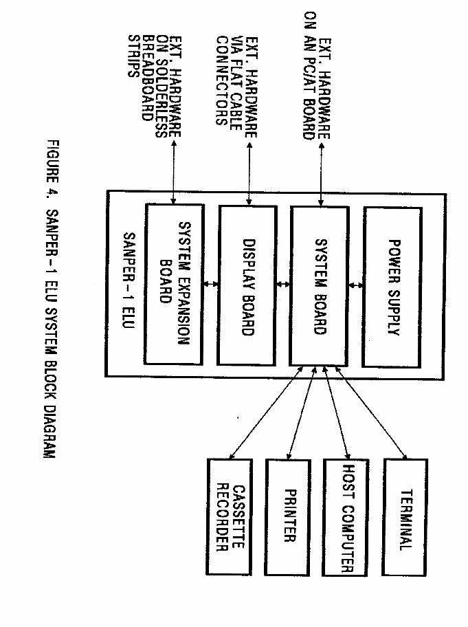
OVERVIEW OF THE SANPER-1 ELU SYSTEM COMPONENTS The SANPER-1 Educational Lab Unit was designed and developed by Dr. Jafar Saniie and Mr. Stephen Perich. The ELU includes a firmware package named “TUTOR” which is a MC68000 resident monitor program developed by Motorola, Inc. The TUTOR program was initially released on a hardware platform called the “MC68000 Educational Computer Board” or ECB, which was also developed by Motorola, Inc. The ECB could be used along with an external power supply and a video display terminal to construct a simple educational development system. While the ECB was an excellent first attempt at an educational development system, the creators of the ELU saw various ways that the ECB could be improved and enhanced. Thus the SANPER-1 ELU is based on the Motorola ECB. Additional features and enhancements have been incorporated into the ELU, thereby transforming it into a standalone MC68000 hardware and software development system. On the ECB, the MC68000 addresses used to access the peripheral I/O devices were hardcoded into TUTOR. In order to port the TUTOR firmware over to the ELU and still retain all of the TUTOR features, the same peripherals had to be included on the ELU. Thus the TUTOR firmware, the two serial port devices and the parallel port device all have the same address ranges as the ECB does. In terms of enhancements, the ELU adds several new peripheral devices such as an A/D Converter, a D/A Converter, a Speech Synthesizer, a parallel port, and two high power output drivers. In addition, the ELU has more memory than its predecessor. The SANPER-1 ELU consists of the following major sub-assemblies:
A. a System Board B. a Display Board C. a System Expansion Board D. a 150-Watt IBM PC/XT compatible power supply E. an IBM PC-compatible chassis F. internal cabling
A brief description of each sub-assembly follows.
A. System Board The System Board is the central control board of the ELU and it contains all the hardware and software needed to implement a complete 68000-based hardware and software development system.
B. Display Board The Display Board contains all the hardware needed to display the status of the 68000 Address, Data, and Control signals. The Address and Data signals are displayed on 7-segment displays. The Control signals are displayed on bargraph LEDs. The Display Board provides the user with access to all of the 68000 Address, Data and Control signals through ribbon cable connectors or the System Expansion Board.
Saniie & Perich SANPER - 1

C. System Expansion Board The System Expansion Board is mounted to the front of the SANPER-1 ELU. It consists of two solderless breadboard strips mounted to a printed circuit board. This board provides the user with access to all the 68000 address, data, and control signals. Each signal is identified on the breadboard strip.
D. Power Supply A 150-Watt power supply supplies power to the System Board, the Display Board, and the System Expansion Board. It is capable of providing the following DC voltages and currents:
• +5V DC @ 15 Amps • -5V DC @ 0.5 Amps • +12V DC @ 5.5 Amps • -12V DC @ 0.5 Amps
The AC input voltage to the power supply can be either 110 VAC or 220 VAC, and is
switch selectable by the user. Notice that the power supply does not provide the user with access to any fuses. This
is due to the fact that the power supply is equipped with short circuit protection. Thus, if a short circuit appears at the outputs of the power supply, the power supply will shut itself off until the short circuit is removed.
E. Chassis The power supply, the System Board and the Display Board are all enclosed in a standard IBM PC-compatible chassis. The chassis has a flip-top lid that provides the user with easy access to the System Board for many purposes including the installation of additional printed circuit boards of the IBM AT Expansion Card form factor.
F. Internal Cabling There are various cables inside the ELU which interface the System Board to the Display Board, the System Expansion Board, and the back panel connectors. All of the cables are keyed to ensure proper installation.
Saniie & Perich SANPER - 2

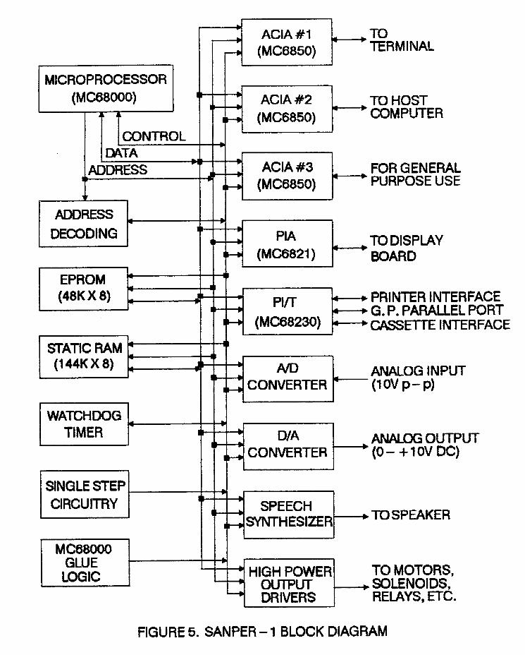
A. SYSTEM BOARD The System Board is equipped with the following peripheral devices:
1. one 16-bit microprocessor (Motorola, MC68000) 2. one Parallel Interface/Timer, PI/T (Motorola, MC68230) 3. one Peripheral Interface Adapter, PIA (Motorola, MC6821) 4. three Asynchronous Communications Interface Adapters, ACIA (Motorola,
MC6850) 5. one 12-bit Analog-to-Digital Converter, ADC (Analog Devices, AD574A) 6. one 12-bit Digital-to-Analog Converter, DAC (Analog Devices, AD7545) 7. one Phoneme Speech Synthesizer (Votrax, SC-02) 8. two high power output drivers (Sprague, UDN2878W-2) 9. 32K bytes of EPROM 10. 208K bytes of static RAM
The System Board also includes various support circuitry necessary for the proper operation of the 68000.
11. MC68000 Support Circuitry
• Power Supply Supervisor and Reset Circuit • Interrupt Request and Interrupt Acknowledge Circuit • Watchdog Timer and Halt Circuit • Synchronous Bus Interface • Asynchronous Bus Interface and Address Decoding • Data Transfer Acknowledge (*DTACK) Signal Generator
The System Board is equipped with the following additional features:
12. Special Features • Expansion Bus Interface • Single-Step Hardware Mode
1. 16-bit Microprocessor (Motorola, MC68000)
The MC68000 is a 16-bit microprocessor whose external address and data buses are 23 and 16 lines wide, respectively. It has a linear address range of 16 mega-bytes.
2. Parallel Interface/Timer, PI/T (Motorola, MC68230)
The MC68230 Parallel Interface/Timer is equipped with double buffered parallel interfaces and a timer. The parallel interfaces operate in unidirectional or bi-directional modes, and can be either 8 or 16 bits wide. The PI/T also has four programmable handshake pins that provide an interface to a wide variety of low, medium and high-speed peripheral devices. The PI/T ports allow use of vectored or autovectored interrupts.
Saniie & Perich SANPER - 3

Within the ELU, the PI/T is used for the following functions: a. Audio Cassette Recorder Interface b. Parallel Printer Interface c. General Purpose Parallel Port d. General Purpose Timer
A description of each function follows. a. Audio Cassette Recorder Interface The MC68230 Parallel Interface/Timer (PI/T) implements the feature of program storage and retrieval on audiocassette tape. The TUTOR monitor program transfers the program to be saved to the PI/T and the PI/T converts it into a stream of serial digital data, which is then converted to an audio signal and sent to the ‘MICROPHONE’ input of an audio tape recorder. To load a program stored on audio tape back into the ELU’s memory, the audio ‘EARPHONE’ output of the tape recorder is converted into digital serial data that is processed by the PI/T. The data is then stored in system memory. This design was originally implemented on the Motorola Educational Computer Board (ECB), and was ported over to the ELU because it provides a simple method of program storage and retrieval. b. Parallel Printer Interface The MC68230 Parallel Interface/Timer (PI/T) provides a Centronics-compatible parallel printer interface. All of the inputs and outputs to the printer are buffered, making it very difficult to accidentally damage the PI/T , or any other component on the System Board. The printer interface allows the user to obtain a hardcopy listing of their program or data. Motorola Inc. publishes an application note that describes the hardware and software required to configure a PI/T for a parallel printer interface. c. General Purpose Parallel Port Rather than configuring the PI/T as a parallel printer port, the student may elect to use the PI/T as a high-speed general-purpose parallel port. Two 8-bit ports (16 digital I/O lines) and 4 handshake lines are made available through a DB-25 connector mounted on the rear panel. One of the ports is configured as input only, and the other port is configured as output only. Similarly, two of the handshake lines are configured as inputs, and the other two are configured as outputs. It is important to remember that when using the parallel port, the printer must be disconnected from the printer port.
Saniie & Perich SANPER - 4

d. General Purpose Timer The PI/T is equipped with a timer that contains a 24-bit wide counter and a 5-bit pre-scaler. The timer can generate a square wave output, periodic interrupts, or a single interrupt after a programmed time period. It can also be used as a watchdog timer, or for elapsed time measurement.
1. Peripheral Interface Adapter, PIA (Motorola, MC6821)
The PIA provides a means of interfacing peripheral equipment to the MC68000 microprocessor. The PIA is equipped with two 8-bit bi-directional I/O ports and 4 control lines. The direction of the I/O lines is programmable, as is the function of the control lines. All twenty of these signals are available on one of the Display Board’s 40-pin ribbon cable connectors and on the System Expansion Board. These signals are not buffer protected so they may be used in any combination of inputs and outputs. The MC68000 communicates with the PIA through the use of the MC68000’s synchronous bus interface. To interface to synchronous peripherals like the PIA, the MC68000 modifies its bus cycle to meet the MC6821 bus timing requirements.
2. Asynchronous Communications Interface Adapter , ACIA (Motorola, MC6850) The ELU is equipped with three ACIAs that serve as serial ports for communicating with various external devices. The first serial port is used for communicating with a terminal (or with a personal computer running terminal emulation software). The second serial port is used for communicating with a host computer (i.e. mainframe, minicomputer, etc.). The third serial port is available for general-purpose use. All three serial ports are configured for the RS-232-C serial communication standard. The ELU is equipped with a baud rate generator that can provide a choice of six different baud rates to each of the ACIAs. The baud rates are hardware selectable through headers P22, P23 and P24. The available baud rates are 9600, 4800, 2400, 1200, 600, 300. The ACIAs communicate with the MC68000 through the use of the MC68000’s synchronous bus interface. To interface to synchronous peripherals like the ACIA, the MC68000 modifies its bus cycle to meet the MC6850 bus timing requirements.
3. 12-bit Analog-to-Digital Converter, ADC (Analog Devices, AD574A) The ELU is equipped with a 12-bit A/D Converter that samples signals ranging from -5V to +5V DC, at a maximum speed of 25 KHz. The analog input signal enters into a sample and hold circuit where it is stabilized, and then inputted to the A/D Converter. The A/D Converter controls the operation of the sample and hold circuit. The A/D Converter forces the Sample & Hold device to hold the data until the A/D Converter has completed the conversion.
Saniie & Perich SANPER - 5
The microprocessor issues a command to the A/D Converter to begin converting. The microprocessor must poll the A/D Converter to determine when the conversion is complete. When the conversion is completed, the microprocessor enables the A/D Converter’s outputs and reads 12 bits of data.
4. 12-bit Digital-to-Analog Converter, DAC (Analog Devices, AD7545) The ELU is equipped with a 12-bit D/A Converter. The D/A Converter is treated as a memory-mapped device. The microprocessor writes data to a certain memory location, and the D/A Converter immediately converts the digital data to an analog voltage. The analog voltage output range is 0 to +5V DC, when an internal -5V DC power source is used as a voltage reference. The user may change the reference voltage to any externally supplied voltage simply by removing a shunt and plugging the new reference voltage into a different connector.
5. Phoneme Speech Synthesizer (Votrax, SC-02)
The ELU is equipped with a phoneme-based speech synthesizer, which is capable of producing an audio output of unlimited vocabulary, music and sound effects. The speech synthesizer allows software control of speech rate, pitch, pitch movement rate, amplitude, articulation rate, vocal tract filter response, and phoneme selection and duration.
6. High power output switches (Sprague, UDN2878W-2)
The ELU is equipped with two 4-bit high power drivers that can be used for driving stepper motors, relays, solenoids, etc. Both drivers are treated as one 8-bit memory-mapped device, with the data being stored in a latch before being sent to the drivers.
7. 32K Bytes of EPROM The System Board is equipped with two banks of EPROMS with 16K bytes per bank. The TUTOR Monitor Program resides in one of these banks. The other bank is available for user programs.
8. 208K Bytes of Static RAM The System Board is equipped with four banks of Static RAM. Three of the banks have 64K bytes per bank, and the fourth bank has 16K bytes per bank. One of the 64K banks (U46 and U72) is configurable for either EPROM or RAM devices. It can contain either two 32K x 8 EPROM or RAM chips. There are 8 sets of jumpers which must be changed if the bank is switched from RAM to EPROM. For the location and correct position of these jumpers, refer to the section entitled “Header Definitions on the SANPER-1 System Board”. This bank is initially configured for RAM.
Saniie & Perich SANPER - 6

9. MC68000 Support Circuitry Miscellaneous circuitry must be added to ensure that the MC68000 operates correctly. a. Power Supply Supervisor and Reset Circuit The ELU is equipped with a circuit that monitors the voltage level of the +5V DC power source, and asserts the MC68000’s *RESET signal input if the voltage drops below +4.5V DC. Thus as the ELU is being powered up or powered down, the MC68000 is held in the reset state until the supply voltage has stabilized and reached the proper range for valid operation. Additionally, the ELU is equipped with a RESET switch on the front panel that provides an easy method of resetting the MC68000 and all other peripheral devices inside the system, without having to power down the ELU. Thus the contents of memory can be retained even if something catastrophic happens to the MC68000. (i.e. a HALT condition) b. Interrupt Request and Interrupt Acknowledge Circuit The ELU is capable of supporting 7 different levels of interrupts. Level 7 is the highest priority interrupt, and level 0 is the lowest. The MC68000 will only recognize and service an interrupt if its priority level is higher than the current priority level existing in the MC68000’s Status Register. The following table illustrates which devices within the ELU are associated with each interrupt level.
Interrupt
Level
Type
Interrupting Device(s) 7 Auto ABORT Switch 6 Auto ACIA #2 (Host interface) 5 Auto ACIA #1 (Terminal interface) 4 Auto ACIA #3, Speech Synthesizer, PIA 3 User PI/T: 16-line Parallel Port 2 User PI/T: 24-bit Timer 1 Auto or User Externally generated 0 ---- None
c. Watchdog Timer and HALT Circuit The ELU is equipped with a watchdog timer, which calculates the length of time of each bus cycle. If any bus cycle exceeds 10 microseconds, the watchdog timer asserts the 68000’s Bus Error (*BERR) input signal, and the 68000 begins BUS ERROR exception processing. This type of watchdog timer is used to identify accesses to memory locations at which no memory or peripheral devices exist, and is not intended to determine software errors such as executing in an infinite loop.
Saniie & Perich SANPER - 7
If the watchdog timer asserts the Bus Error (*BERR) input signal on two consecutive bus cycles, the 68000 decodes this as a HALT condition and asserts its HALT signal as an output. The System Board’s HALT circuit then illuminates the LED labeled “LED1”. d. Synchronous Bus Interface The 68000 has the ability to interface to both synchronous and asynchronous devices. Synchronous devices are those which require a clock input, and whose data transfer is synchronized to this clock signal. The 68000 has a built-in synchronous interface. The MC6800 was originally designed for interfacing to previously mentioned synchronous devices such as the ACIA (MC6850), and the PIA (MC6821). The MC6800 only permits synchronous data transfers between its peripheral devices. The hardware on the System Board has been designed to facilitate the synchronous bus interface. e. Asynchronous Bus Interface and Address Decoding The MC68000-type peripherals are asynchronous; they do not require a clock input.
f. Data Transfer Acknowledge (*DTACK) Signal Generator The *DTACK signal is externally generated during asynchronous bus cycles to inform the 68000 of the conclusion of a bus cycle. Due to the fact that different peripheral devices operate at different speeds and access times, the *DTACK signal generator was designed to assert the *DTACK signal at different times depending on which device was being accessed.
10. Special Features
a. Expansion Bus Interface If a user wishes to design his/her own hardware and test it on the ELU, he/she must place the circuit on an IBM PC/XT/AT compatible expansion board. This board can then be installed in one of four expansion slots present on the System Board. Each slot is provided with all the MC68000 Address, Data and Control signals, as well as with four board selection lines. These selection lines are independently activated according to the Memory Map illustrated in Table 1. Each slot is provided with the four selection lines so that placement of the user’s board will be slot independent. Each expansion board must use a unique board selection line. The IBM PC/AT expansion bus card form factor was chosen because these boards are inexpensive and readily available in both wire-wrap and solder-type styles.
Saniie & Perich SANPER - 8

The user can place any type of hardware design on the expansion boards. Some examples of circuits that can be implemented on expansion boards are: floppy disk controllers, expansion memory, digital I/O, analog I/O, Digital Signal Processor, IEEE-488 bus interface, Eprom programmer, etc. b. Single-Step Hardware Mode The single step circuitry allows the user to observe every bus cycle of the 68000 in a static state. When the user changes one of the front panel toggle switches from “FREE RUN” to “SINGLE STEP”, and sets another toggle switch to the “S.S.- SYS.” position, the 68000 executes only one bus cycle at a time. The MC68000’s address, data, and control signals are frozen in time, and are displayed on the Display Board. Only when the user presses the “SINGLE STEP PULSE” pushbutton switch does the microprocessor advance to the next bus cycle. This is an extremely valuable learning tool, because the user can observe all the intermediate steps that occur during the execution of a single 68000 instruction. There is a more detailed explanation of the Single Step Hardware Mode in the Display Board Overview section.
Saniie & Perich SANPER - 9

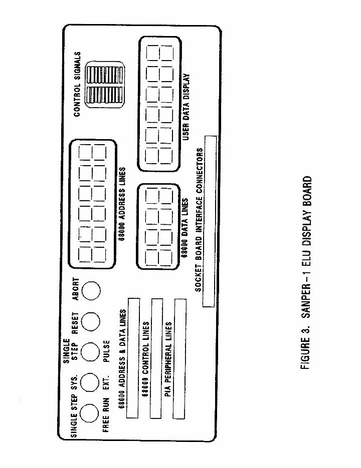
B. DISPLAY BOARD The Display Board provides a visual indication of the status of the MC68000 by displaying the current address, data, and control signals. The Display Board consists of the following entities:
1. Switches 2. Status Displays 3. System Expansion Board connectors 4. Front Panel Expansion connectors
1. Switches
There are five switches mounted on the Front Panel of the SANPER-1 ELU. These switches are used to control events on the System Board. The two leftmost switches are toggle switches, and the three rightmost switches are pushbutton or momentary type switches. From left to right, the switches are labeled as follows: a. SINGLE STEP / FREE RUN b. S.S. – SYS. / S.S. – EXT.
(System Single Step / External Single Step) c. SINGLE STEP PULSE a. RESET b. ABORT a. Single Step /Free Run Toggle Switch This switch determines whether the System Board is operating in either the “Free Run” or “Single Step” mode. In the “Free Run” mode of operation, the MC68000 microprocessor will continually execute one instruction after another without stopping. In the “Single Step” mode, the MC68000 will execute only one bus cycle at a time. The values of the MC68000 Address and Data Bus signals are shown on the seven segment displays. The states of the MC68000 Control signals are shown on the bargraph displays. The user must depress the “Single Step Pulse” switch in order to advance to the next bus cycle. b. System Single Step / External Single Step Tpggle Switch This toggle switch determines which Single Step sub-mode the System Board is operating in. In the “External Single Step” mode, the System Board will single step through only those instructions which access devices located in the address ranges specified by the Block Select Lines (BB-*Q5 through BB-*Q8) and (*Q11 through *Q14).
Saniie & Perich SANPER - 10

One set of Block Select Lines (BB-*Q5 through BB-*Q8) are only accessible through the System Expansion Board or the Front Panel Expansion Connectors. The other set of Block Select Lines (*Q11 through *Q14) are only accessible through the four 98-pin AT style connectors mounted on the System Board. This mode is useful when the student is interfacing his/her external hardware to the SANPER-1 ELU. Using this mode the student can single step through only those instructions which address their hardware. This avoids single stepping through either the TUTOR firmware or other software that does not directly address the prototype hardware. While single stepping, the only way to advance to the next bus cycle is to depress the Single Step Pulse pushbutton switch. In the “System Single Step” mode, the System Board will single step through all instructions regardless of the address space it is addressing. The word “System” applies to both internal and external memory accesses. Thus the student can single step through the TUTOR firmware as well as any other piece of software. While single stepping, the only way to advance to the next bus cycle is to depress the Single Step Pulse pushbutton switch. c. Single Step Pulse Pushbutton Switch
This pushbutton switch is used in conjunction with the two toggle switches previously mentioned above. Depressing this switch serves to advance the MC68000 to the next bus cycle. This switch is only active when the System Board is operating in the “Single Step” Mode. It must be depressed in order to advance to the next bus cycle regardless of which single step sub-mode has been selected (External or System). d. Reset Pushbutton Switch
This pushbutton switch pulls the System Board’s *RESET signal to a low TTL logic level, which reinitializes the MC68000 and some of the MC68000’s peripheral devices such as the PIA, the PI/T, the Speech Synthesizer, and the High Output Driver. Immediately after the *RESET line goes high again, the MC68000 begins loading the Exception Vector Table from the TUTOR EPROM into static RAM. All of the MC68000’s internal registers are initialized. This switch should only be used for recovering from serious faults such as a HALT condition, and cannot be used as an aid in debugging software, since the status of the internal registers is lost. e. Abort Pushbutton Switch
Saniie & Perich SANPER - 11
This pushbutton switch generates a Level 7 interrupt to the MC68000, which immediately loads the exception vector for a Level 7 Autovectored Interrupt. The Level 7 Interrupt Service Routine halts execution of the current program, and outputs a status message to the terminal or personal computer. The service routine outputs the phase “SOFTWARE ABORT” along with the contents of each of the MC68000’s internal registers. This switch is useful for breaking out of a user program without losing the status of the internal MC68000 registers or the contents of memory.
2. Status Displays
a. Seven Segment Displays There are three sets of seven segment displays on the Display Board. One set is used for the MC68000 Address Lines, the second set for the MC68000 Data lines, and the third set for the User Data Display. Address Lines The first set of seven segment displays consists of 6 hexadecimal digits, which annunciate the status of the MC68000 Address lines. The possible range of values is from $000000 to $FFFFFF. These digits are visible only when the SANPER-1 ELU is in the “Single Step” Mode. In “Free Run” Mode these displays are off. Data Lines The second set of displays consists of 4 hexadecimal digits, which annunciate the status of the MC68000 Data lines. The possible range of values is from $0000 to $FFFF. These digits are visible only when the SANPER-1 ELU is in the “Single Step” Mode. In “Free Run” Mode these displays are off. User Data Display The third set of displays consists of six hexadecimal digits and serves as a general-purpose user display. These displays are treated as two memory-mapped peripherals, and are write only. One memory location addresses the four least significant digits, and the other memory location addresses the two most significant digits. When writing data to the display, simply write the exact hexadecimal value you wish to see appear on the display. No BCD-to-hexadecimal conversion is required. The user accesses the lower four digits of the display by executing a write operation (of length “word”) of an 16-bit hexadecimal data value to location $90000. An instruction which would perform this task is “MOVE.W #$3456, $90000”. The “$” denotes hexadecimal notation. The user accesses the upper two digits of the display by executing a write operation (of length “byte”) of an 8-bit hexadecimal data value to location $A0000. An instruction which would perform this task is “MOVE.B #$12, $A0000”.
Saniie & Perich SANPER - 12

The final result on the User Data Display is “123456”. Thus the possible range of values that can be displayed is from $000000 to $FFFFFF. The System Board generates a *DTACK pulse to the MC68000 every time a write operation is performed to this display. These digits are always illuminated regardless of whether the SANPER-1 ELU is in the “Single Step” Mode or the “Free Run” Mode. b. Bargraph Displays There are two bargraph displays on the Display Board which are used for annunciating the status of the MC68000 Control Signals. Each display contains a maximum of ten individual LEDs. The two bargraph displays can be divided into a left and a right display. Left Bargraph Display Right Bargraph Display Mnemonic – Full Name Mnemonic – Full Name _____ BERR – Bus Error
FC2 – Function Code 2
__ AS – Address Strobe
FC1 – Function Code 1
_____ HALT - Halt
FC0 – Function Code 0
____ UDS – Upper Data Strobe
__ BR – Bus Request
______ RESET – Reset
__ BG – Bus Grant
____ LDS – Lower Data Strobe
_______ BGACK – Bus Grant Acknowledge
_______ DTACK – Data Transfer Acknowledge
____ IPL2 – Interrupt Priority Level 2
__ R / W – Read / Write
____ IPL1 – Interrupt Priority Level 1
____ VPA – Valid Peripheral Address
____ IPL0 – Interrupt Priority Level 0
____ VMA – Valid Memory Address
blank – not used
Saniie & Perich SANPER - 13

__ Note that a bar over the signal name (e.g. AS), implies that the signal is asserted active low (voltage level: 0.0 to 0.8 Volts). Similarly, any signal without a bar over its name (i.e. FC2), is asserted active high (voltage level: 2.4 to 5.0 Volts). Also note that a signal can be denoted as active low by preceding its name with an asterisk (e.g. *AS). This latter case is how active low signals are generally denoted throughout this manual. When one of the LEDs on the bargraph display is lit, this implies that the signal is in its active state. The voltage level associated with the active state is dependent on whether the signal is active low or active high. For example, if the LED for the *AS signal is lit, this implies that the signal is asserted, and its voltage level is in the range of 0.0 to 0.8 Volts. The one special case in the group is the R/*W signal. When a MC68000 Read operation is taking place, the LED is lit, and the signal is asserted active high. When a MC68000 Write operation is taking place, the LED is off, and the signal is asserted active low. The bargraph displays are always on regardless of whether the SANPER-1 ELU is in the “Free Run” or “Single Step” Mode.
3. System Expansion Board Connectors
There are two connectors on the Display Board which supply all the System Board signals to the System Expansion Board. The two connectors each contain 50 female pins, and are located in the bottom center of the Display Board. There are two connectors on the System Expansion Board. These connectors each contain 50 male pins. The male connectors on the System Expansion Board interconnect with the female connectors on the Display Board.
4. Front Panel Expansion Connectors
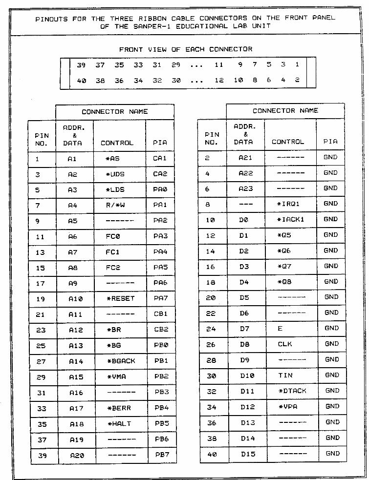
There are three connectors on the Display Board which allow the user to interface external hardware to the SANPER-1 ELU. Each of the connectors provides a certain set of signals. The top connector provides the MC68000 Address and Data Signals. The middle connector provides the MC68000 Control Signals, and the bottom connector provides the PIA Peripheral Bus Signals. Each of the connectors contains 40 male pins, and is designed to interconnect to a 40-pin female connector through a 40-pin ribbon cable. The pinout for each of the three connectors is shown in Figure TBD. If the student is using the Block Select Lines (labeled “BB-*Q5” through “BB-*Q8”) to select their external hardware devices, then they must also design external circuitry
Saniie & Perich SANPER - 14

to generate a *DTACK signal input to the MC68000 at the conclusion of the bus cycle.
C. SYSTEM EXPANSION BOARD The System Expansion Board is mounted to the front of the SANPER-1 ELU. It consists of a two solderless breadboard strips mounted to a printed circuit board. In addition to the providing the MC68000, MC68230, and MC6821 signals, it also provides the user with +5V DC and +5V DC return (ground) for supplying power to the external devices. Each signal on the System Expansion Board is clearly marked. Figure TBD shows the location of each signal on the board. The available signals are:
• MC68000 Address Lines: (A1 to A23) • MC68000 Data Lines: (D0 to D15) • MC68000 Asynchronous Bus Control Lines:
(*AS, *UDS, *LDS, R/*W, *DTACK) • MC68000 Synchronous Bus Control Lines:
(E, *VPA, *VMA) • MC68000 Bus Arbitration Lines:
(*BR, *BG, *BGACK) • MC68000 Function Code Lines: (FC2, FC1, FC0) • MC68000 System Control Lines:
(*RESET, *HALT, *BERR, CLK) • MC68000 Level 1 Interrupt and Int. Acknowledge Lines:
(*IRQ1, *IACK1) • System Board Block Select Lines: (*Q5, *Q6, *Q7, *Q8) • MC68230 Timer Input: (TIN) • MC6821 Peripheral Data Lines: (PA0 to PA7, PB0 to PB7) • MC6821 Peripheral Control Lines: (CA1, CA2, CB1, CB2)
If the user has designed additional hardware on a separate solderless breadboard, he/she may interface their board to the SANPER-1 ELU through the use of the System Expansion Board. First the user must obtain several pieces of 26 AWG. solid telephone wire, and cut these pieces to an approximate 3” to 6” length. Then the user should strip 0.25” off each end of the wire. With the SANPER-1 ELU turned off, the user should insert one end of the wire into the System Expansion Board, and the other end into he/his own breadboard strip. The user should repeat this procedure until all connections are complete. Then the SANPER-1 ELU may be turned on.
Saniie & Perich SANPER - 15

F. INTERNAL CABLING Inside the SANPER-1 ELU there are several cables which serve to interface the System Board to the Display Board, the System Expansion Board, the back panel connectors, and a speaker. 1. Display and System Expansion Board Interfacing
a. Signals There are two 40-pin ribbon cable assemblies that bring the 68000’s Address, Data and Control signals out from the System Board to the Display Board. There is an additional 40-pin ribbon cable assembly that brings the PIA’s peripheral lines out from the System Board to the Display Board. b. Power +5V DC power is supplied to the Display Board through a discrete two wire cable.
2. Back Panel Connector Interfacing
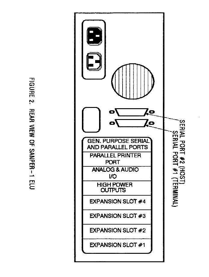
a. A/D and D/A Interfacing There is one coaxial cable assembly that makes the System Board’s D/A Converter output available to the user at the back of the lab unit. There is another coaxial cable assembly that makes the System Board’s A/D Converter input available to the user at the back of the lab unit. b. Audio Port Interfacing There is one discrete wiring assembly that makes the System Board’s audio input and output ports available to the user at the back of the lab unit. c. High Power Driver Interfacing There are two discrete wiring assemblies which originate at the System Board and carry the high power driver outputs to an expansion bus bracket mounted on the back of the chassis. d. Serial and Parallel Port Interfacing There is a ribbon cable assembly for each of the serial and parallel ports on the System Board. Specifically, here is one cable assembly for each of the three serial ports, the general purpose parallel port and the parallel printer port. All of these ports are available to the user at the back of the lab unit.
Saniie & Perich SANPER - 16
Saniie & Perich SANPER - 17
The serial ports are terminated in DB-25 plug connectors (male pins), and the parallel ports are terminated in DB-25 receptacle connectors (female pins).
3. Speaker Interfacing Speech Synthesizer Interfacing The System Board’s speech synthesizer output is connected by means of a two-wire assembly to an 8 ohm speaker mounted on the front panel of the chassis.


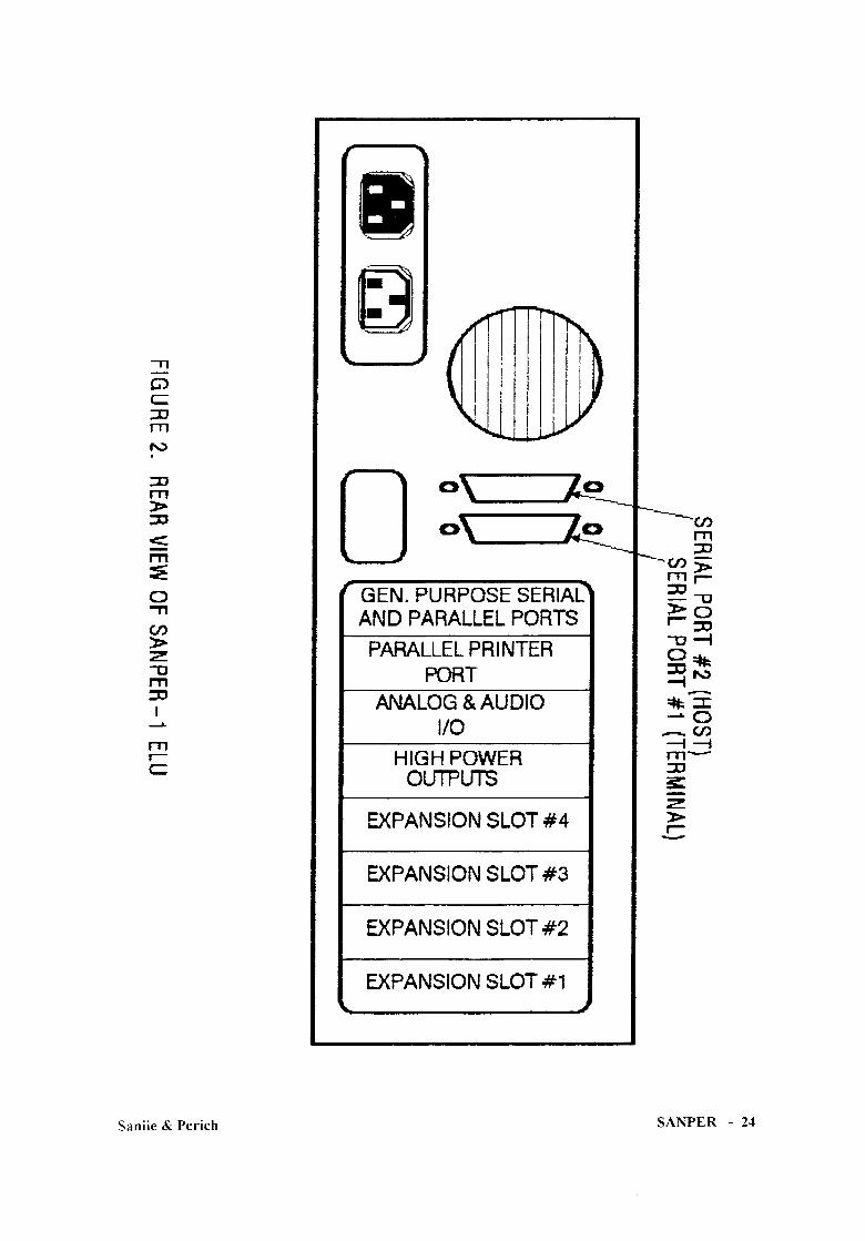
GEN. PURPOSE SERIALAND PARALLEL PORTSPARALLEL PRINTER
PORTAAIALOG & AUDIO
VOHIGH POWEROUTPUTS
EXPANSION SLOT #4
EXPANSION SLOT #3
EXPANSION SLOT #2
FXPANSION SLOT #1
rnv
TO--l
+l\)
(r)rrl:'f
>|--E
Ofr-{
: * =r l a
n C/f)- - l
=t==
-Tl
aE=trnP=,rrl
F
rTt=
o
u)z.-Er7I=t
r-nG
Saniie & Perich SANPER - 21

ACIA #1(MC685o)
MICROPROCESSOR(MC68ooo)
ACIA #3(MC685o)
HIGH POWEROUTPUTDRIVERS
MNTROL
TOTERMINAL
TO HOSTCOMPUTER
FOR GENERALPURPOSE USE
TO DISPIAYBOARD
PRINTER INTERFACEG- P. PARALLEL PORTCASSETTE INTERFACE
AIIALOG INPUT(10V p- p)
AhIAI.OG OUTPUT(o- +1ov Dc)
TOSPEAKEB
TO MOTORS,SOLENOIDS.REIAYS, ETC.
Sani ie & Per ich
FIGURE 5. SANPER - 1 BLOCK DIAGRAM
SANPER - 27
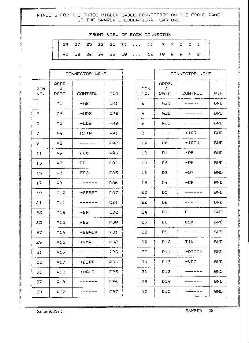
F , I N O U T S F O R T H E T H R E E R I B B O NO F T H E S A N F , E R - 1
C E B L E C O N N E C T O R SE D U C A T I O N R L L R B
ON THE FROI\ ]T F 'ATIELU N I T
F R O N T V I E W O F E A C H C O N N E C T O R
39 37
4A i8
: ? ? t . : , oU g J I L J
3 4 3 t 3 0
7 5 3 1
8 6 4 e
1 1
l H
?E;
36
9
1 E
CONNECTOR NEMt
I F , r NI N O .
R D D R .&.
DETA C O N T R O L F , I Q
If H I * A S
RE * U D S C R E
J R 3 *LDS Ff ,A
7 A 4 R / * W p R 1
9 N FH J F,AI
l . lr t R6 F C E F'R3
6 ( F'44
1 5 R 8 FCe F ' H J
t 7 R9 F.R6
1 9 A 1 0 *RESET t s H I
t1 1 R 1 1
e3 H I I : *BR
e5 R 1 3 *BG F,BIZI
A l 4 *BGACK F'B 1
t 9 n l EH T J * V M R F'BI
H L c tp B 3
*BERR F.B4
35 R 1 8 *HALT P B 5
37 A 1 9 F'85
39 Aeo p B 7
F ' I NN O .
Q D D R . I& lD R T R I C O N T R O L F . ] R
H ; I GND
+ A c i G N D
6 R : 3 6ND
I * I R G 1 GND
1 tzl D A * I A C K 1 CND
1 E D 1 +O5 GIID
t 4 D J *G6 6ND
l c l D 3 *47 G N D
D 4 *n8 GNI)
:o D 5 ( J I \ ] J
EE D€. GND
e4 D 7 E G N D
e5 D 8 LLI-r GND
e8 D 9 G N D
3 0 D l o T I N GN]]
I J I I * D T R C K GNi]
34 D l e *VF,A l ' : ' I \ I J
f,6 D 1 3 G N D
3t1 D l 4 G N D
4tZ D 1 5 G N D
Sani ie & Per ich SANPER 30