Embed Size (px)
Citation preview
UUSSEERR’’SS MMAANNUUAALL
DC TO AC CONVERTERSINGLE PHASE INVERTERREF. CO-1020 BENCH


http: // WWW.LANGLOIS-FRANCE.COM
APPLIED PHYSICS
PEDAGOGICAL MANUAL
DC TO AC CONVERTERSINGLE PHASE INVERTER
CO-1020 BENCH
Author H. OBEIDI
Translation: F. FALCO
Lecturers in Applied Physics

1
TABLE OF CONTENT
PREAMBLE
3
INTRODUCTION 4
THE CO-120 BENCH 6
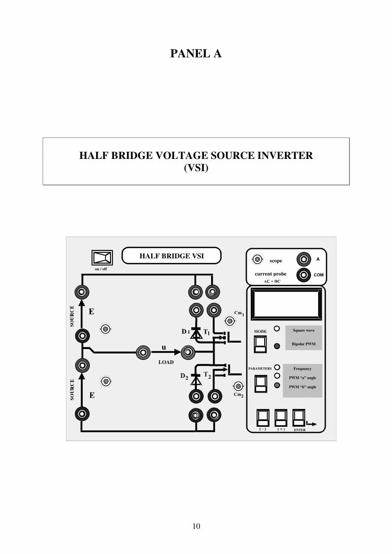
PANEL A “Half bridge voltage source inverter” 10
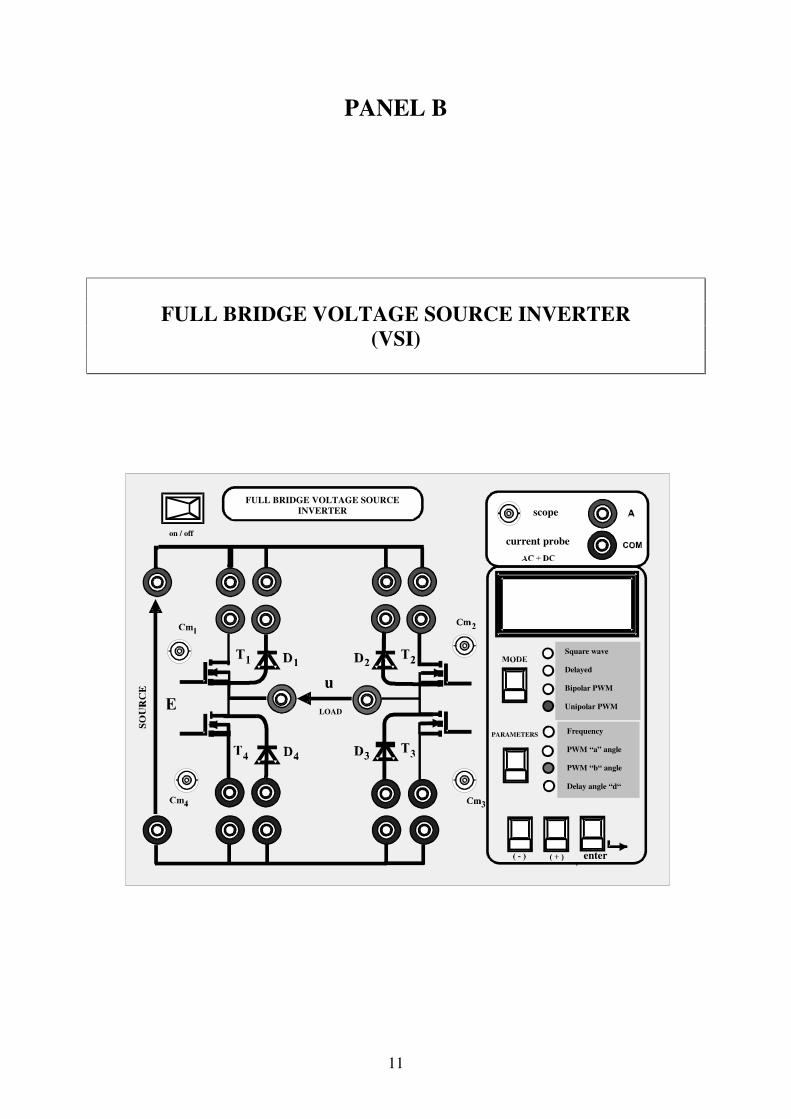
PANEL B “Full bridge voltage source inverter” 11
PANEL A 12
PANEL B 15
WAVEFORM OBSERVATIONVOLTAGE AND CURRENT CHARACTERISTICS 18
TECHNICAL SPECIFICATIONS 19
I Security, environment and EMC 19II Electrical characteristics 21III Safety and directions for use 24IV Components replacement 25
VOLTAGE SOURCE INVERTERWAVEFORMS AND SWITCHING COMMAND 26
I Switching 26II Square wave command 27III Delayed command 29IV Bipolar PWM 31V Unipolar PWM 34

2
LABORATORY WORKHALF BRIDGE VOLTAGE SOURCE INVERTER 39
Resistive load 42Inductive load 51Resonant load 56
LABORATORY WORKFULL BRIDGE VOLTAGE SOURCE INVERTER 62
Resistive load 63Inductive load 80Resonant load 87Induction heating 93Emergency power supply 98Induction motor drive system 101

3
PREAMBLE
The improvement of silicon controlled rectifiers, SCRs, led to the development
of a new area of applications called power electronics.
Power electronics deals with controlled and conversion of electrical power of
semiconductors devices wherein these devices operate as switches. Since the
SCRs are available the application area spread to many fields such as motor-
drives, power supplies, aviation electronics, electronics converters…
The main task of power electronics is to control and convert electrical power
from one form to another.
The CO-120 bench is a pedagogical device which illustrates the concept of AC
waveform generation. It is a DC to AC converter and deals with half bridge and
full bridge configurations.
4
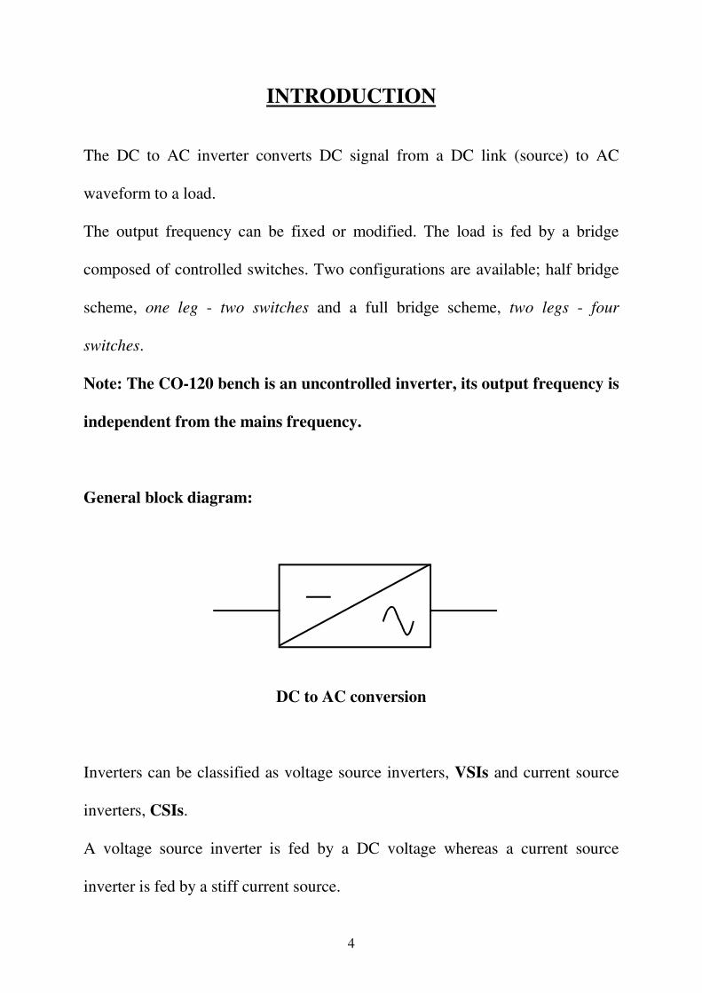
INTRODUCTION
The DC to AC inverter converts DC signal from a DC link (source) to AC
waveform to a load.
The output frequency can be fixed or modified. The load is fed by a bridge
composed of controlled switches. Two configurations are available; half bridge
scheme, one leg - two switches and a full bridge scheme, two legs - four
switches.
Note: The CO-120 bench is an uncontrolled inverter, its output frequency is
independent from the mains frequency.
General block diagram:
DC to AC conversion
Inverters can be classified as voltage source inverters, VSIs and current source
inverters, CSIs.
A voltage source inverter is fed by a DC voltage whereas a current source
inverter is fed by a stiff current source.

5
The CO-120 bench feeds resistive load, inductive load, resonant load and AC
motors.

6
THE CO-120 BENCH
Every single phase inverter configuration can be studied with the CO-120 bench.
Fundamentals of power conversion are organized in chosen laboratory works.
This pedagogical bench can be used either in secondary degrees, school of
engineering or Polytechnic departments.
Half bridge voltage source inverter:
Commonly called inverter leg, this configuration needs a central point power
supply.
This is the basic scheme for the understanding of full bridge, three phase and
higher order inverters.
7
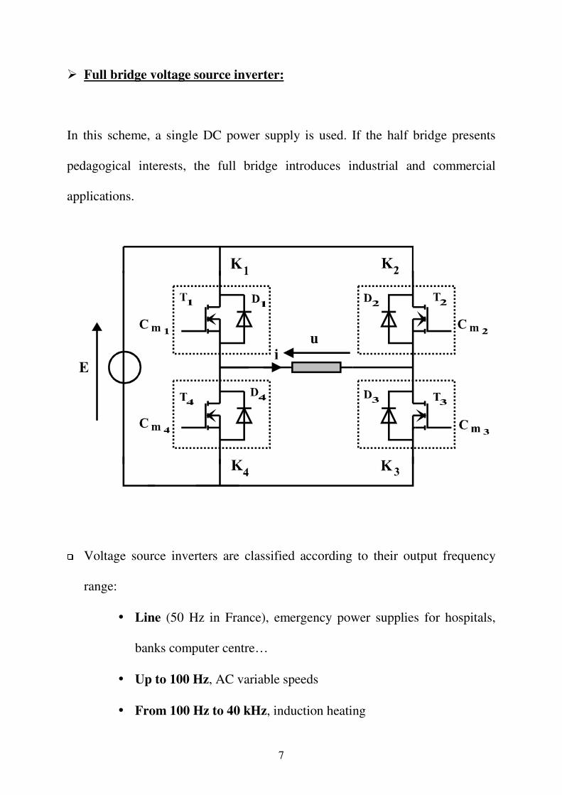
Full bridge voltage source inverter:
In this scheme, a single DC power supply is used. If the half bridge presents
pedagogical interests, the full bridge introduces industrial and commercial
applications.
Voltage source inverters are classified according to their output frequency
range:
• Line (50 Hz in France), emergency power supplies for hospitals,
banks computer centre…
• Up to 100 Hz, AC variable speeds
• From 100 Hz to 40 kHz, induction heating

8
The CO-120 is made of two parts:
• Inverter scheme (half or full bridge)
• Command board dedicated to switching control (output frequency,
command mode, PWM…). Controlled switches are driven by a
microcontroller.
Practically the bench is very easy to use: two front panels are available,
half bridge scheme (Panel A) and full bridge scheme (Panel B).
Once the bridge configuration is chosen, user can easily plug DC power supply,
loads, meters, scope, current probe… thus the lecturer is able to verify
efficiently every benches.
Note: Printed circuit and electronics board are protected by resettable
switches called “polyswitches”.
The Pulse Width Modulation command is very flexible, it can be modified from
the command board. This desk monitors pulse width, output frequency and
switching angles are displayed (LCD). The output waveform can be improved
with the harmonic control using spectrum analyser or a scope including a
spectrum analyser.

9
Note: in order to underline the uncontrolled characteristic of the inverter,
mains can be replaced by batteries for electronics circuits and the DC link
can be replaced by a battery of accumulator instead of a DC power supply.
Thus the inverter is line free.
10
PANEL A
HALF BRIDGE VOLTAGE SOURCE INVERTER(VSI)
PRESENTATION DE LA FACE B
HALF BRIDGE VSI
on / off
LOAD
scope
current probe
Square wave
Bipolar PWM
Frequency
PWM “a” angle
PWM “b” angle
ENTER
PARAMETERS
11
PANEL B
FULL BRIDGE VOLTAGE SOURCE INVERTER(VSI)
FULL BRIDGE VOLTAGE SOURCEINVERTER
on / off
LOAD
scope
current probe
Square wave
Delayed
Bipolar PWM
Unipolar PWM
Frequency
PWM “a” angle
PWM “b“ angle
Delay angle “d“
enter
PARAMETERS
12
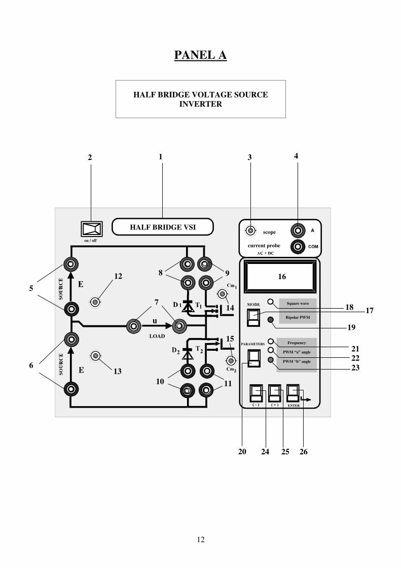
PANEL A
HALF BRIDGE VOLTAGE SOURCEINVERTER
HALF BRIDGE VSI
on / off
LOAD
scope
current probe
Square wave
Bipolar PWM
Frequency
PWM “a” angle
PWM “b” angle
ENTER
5
6
2 1 3 4
12
13
7
8 9
10 11
14
15
16
18 17
19
20
212223
24 25 26
PARAMETERS

13
1 Inverter scheme
2 Power
3 Scope output, used to visualized current: 1 V/A
4 Current probe Imax 3A
5 DC link (centre point) +E
6 DC link –E
7 AC load, Imax 3A
8 Current into D1 diode. Current probe for visualization or meter formeasuring intensity.
9 Current into T1 transistor.
Note: a strap wire must be connected if no current characteristics in theleg is required.
10 Current into D2 diode
11 Current into T2 transistor
12 Unused with Panel A
13 Unused with Panel A
14 T1 command signal
15 T2 command signal
16 Display (LCD). When square wave mode is selected output frequencyis displayed. When bipolar PWM mode is selected output frequencyand switching angles are displayed.
17 Switching command
Note: by default square wave is engaged when power is turned on. Press17 to modify switching command.

14
18 Red light on when square wave mode is selected
19 Red light on when bipolar PWM is selected
20 Once the switching command is fixed output frequency and switchingangles can be modified:
a. When square wave mode is able the output frequency can bemodified only
b. When bipolar PWM mode is able both output frequency andswitching angles can be modified
Note: by default square wave command and 100 Hz output frequency areset when power is turned on.
21 Green light on when output frequency is being modified
22 Green light on when first switching angle of PWM is being modified
23 Green light on when second switching angle of PWM is beingmodified
24 Every time 24 is pressed, output frequency is decreased an amount of 1Hz
25 Every time 24 is pressed, output frequency is increased an amount of 1Hz
Note: press long time 24 or 25 if the required value is high.
26 Enter. Press 26 every time a parameter or a command mode ismodified.
Note: the 0 V level voltage of the bench power supply, the low voltage of thebridge and 3, 14 and 15 are grounded.
15
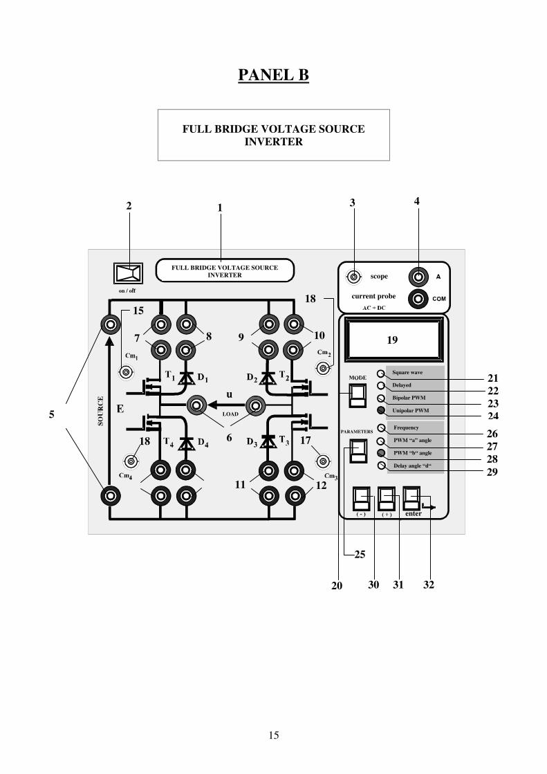
PANEL B
FULL BRIDGE VOLTAGE SOURCEINVERTER
FULL BRIDGE VOLTAGE SOURCEINVERTER
on / off
LOAD
scope
current probe
Square wave
Delayed
Bipolar PWM
Unipolar PWM
Frequency
PWM “a” angle
PWM “b“ angle
Delay angle “d“
enter
PARAMETERS
12 3 4
5
6
7 8 9 10
11 12
18
1518
17
19
21222324
26272829
30 31 32
25
20

16
1 Inverter scheme
2 Power
3 Scope output, used to visualized current: 1 V/A
4 Current probe Imax 3A
5 DC link
6 AC load
7 Current into transistor T1
Note: a strap wire must be connected if no current characteristics in theleg is required.
8 Current into diode D1
9 Current into diode D2
10 Current into transistor T2
Note: a strap wire must be connected if no current characteristics in theleg is required.
11 Current into diode D3
12 Current into transistor T3
Note: a strap wire must be connected if no current characteristics in theleg is required.
13 Current into transistor T4
Note: a strap wire must be connected if no current characteristics in theleg is required.
14 Current into diode D4
15 T1 command signal
16 T2 command signal

17
17 T3 command signal
18 T4 command signal
19 Display (LCD). When square wave is selected output frequency isdisplayed.
When delayed mode is selected, both output frequency an delay angle aredisplayed. When bipolar or unipolar mode are selected, both outputfrequency and PWM angles are displayed.
20 Switching command.
Note: by default square wave is engaged when power is turned on. Press 20to modify switching command.
21 Red light on when square wave mode is selected
22 Red light on when delayed mode is selected
23 Red light on when bipolar PWM mode is selected
24 Red light on when unipolar PWM mode is selected
25 Parameters
26 Green light on when output frequency is being modified
27 Green light on when PWM first angle is being modified
28 Green light on when PWM second angle is being modified
29 Green light on when delay angle is being modified
30 Every time 30 is pressed the output frequency, the first and secondPWM angle are decreased respectively an amount of 1 Hz or 1°.
31 Every time 30 is pressed the output frequency, the first and secondPWM angle are increased respectively an amount of 1 Hz or 1°.
32 Enter. Press 30 every time a parameter or a command mode ismodified.
18
WAVEFORM OBSERVATION / VOLTAGE AND CURRENTCHARACTERISTICS
1 Waveform / voltage measurement
Caution: short circuits may occur if user does not remember that manyparts of the bench are grounded. Differential probes or differentialchannels scope must be used when two different waveforms arevisualized.
Note:
Low frequency: use CHOP sweeping mode
Trigger (sweeping): use Level button
DC mode: full signal, both mean value and wave are displayed
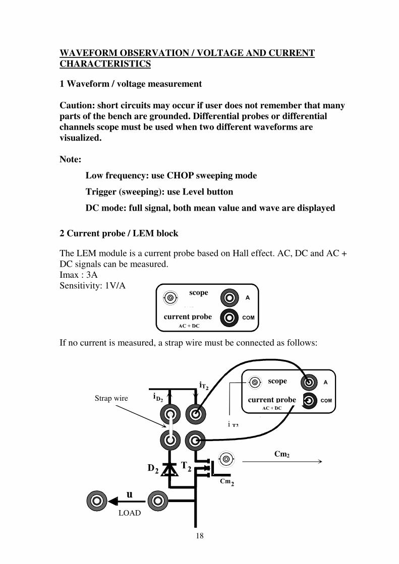
2 Current probe / LEM block
The LEM module is a current probe based on Hall effect. AC, DC and AC +DC signals can be measured.Imax : 3ASensitivity: 1V/A
If no current is measured, a strap wire must be connected as follows:
scope
current probe
scope
Strap wire
i T2
Cm2
scope
current probe
LOAD

19
TECHNICAL SPECIFICATIONS
I SECURITY, ENVIRONMENT AND EMC
A SECURITY
This product complies with secured voltages:
Less than 50 Vrms (AC)Less than 120 V (DC)
USER BRIDGE STRUCTURESWITCHINGCOMMAND
NO PANEL BENCH OFF NONE
PANEL A HALF BRIDGE SQUARE WAVEBIPOLAR PWM
PANEL B FULL BRIDGE SQUARE WAVEPWM
DELAYED
Refer servicing to qualified service personnel only.
B ENVIRONMENT
Use: + 10 °C to 40 °C
Storage: to prevent fire or electrical shock hazard do not expose thisproduct to rain, dust or moisture.

20
C EMC
This bench complies with EMC rules
II ELECTRICAL CHARACTERISTICS
A DC LINK
Two kinds of DC power supply can be used:
o Desk power supply
Ref GPC 3030 90 VA
CO-100 bench
Note: high capacitors must be added in order to make the power supplyreversible.
o Battery
12V / 24 V ref CO 106
1 Half bridge – VSI
A central point power supply or a couple of batteries must be used. Asymmetrical power supply is obtained with two capacitors which have the samevalue. Then the DC link is equally “split” into two.
2 Full bridge – VSI
A desk power supply or a single battery can be used. 12 V or 24 V sourcevoltage

21
B Electronic circuit
The electronic board must be supplied by a symmetrical power supply +/- 15 V.Connections are situated at the rear side of the bench.
C Power electronic devices
1 Rectifier diode
In case of default or damage, diode can be replaced by the following devices:
RectifierPLASTIC PACKAGE
TO 194PLASTIC PACKAGE
TO 220 AC
IFAV ou Io 5 A 8 A
100 MR 821 MUR 810
200 MUR 822 MUR 820VRRM
400 MR 824 MUR 840
22
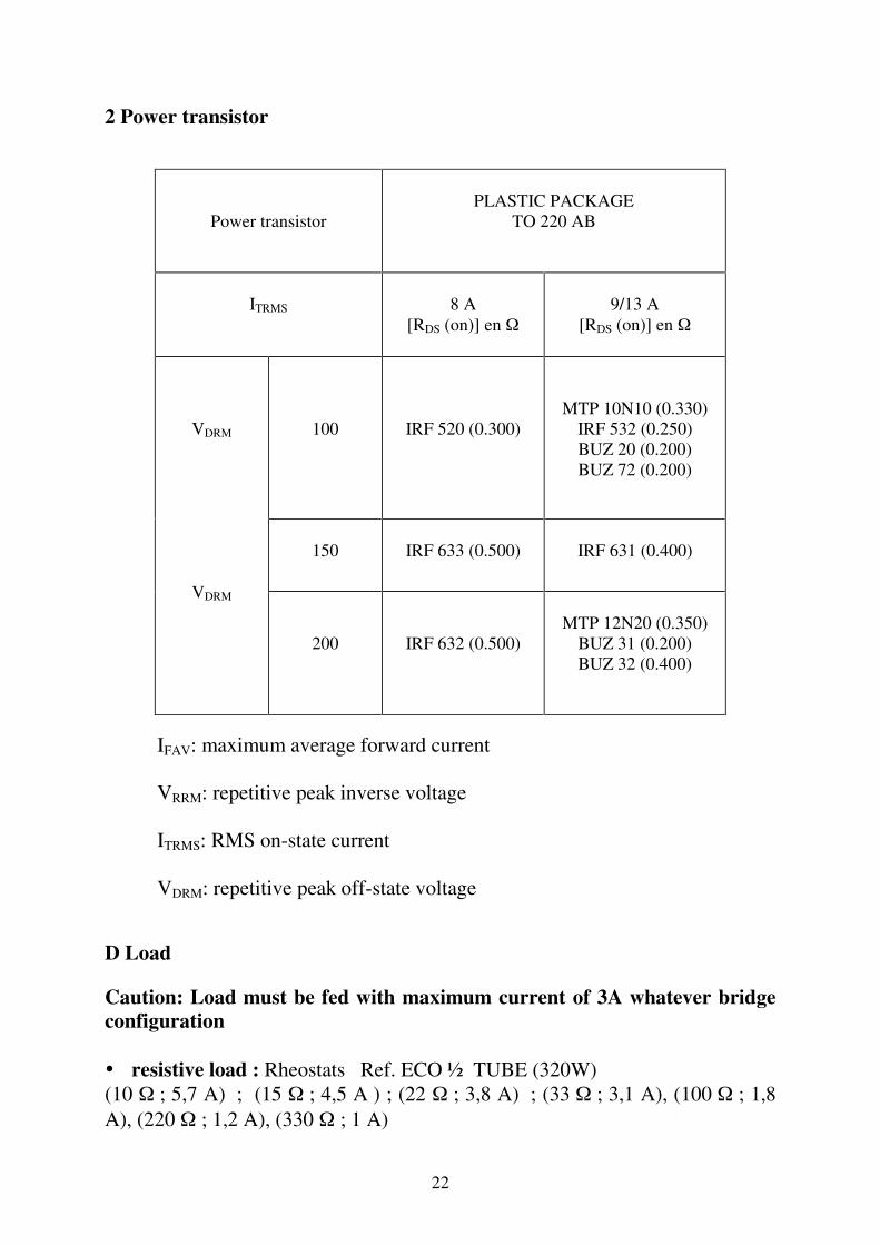
2 Power transistor
Power transistorPLASTIC PACKAGE
TO 220 AB
ITRMS 8 A[RDS (on)] en Ω
9/13 A[RDS (on)] en Ω
100 IRF 520 (0.300)MTP 10N10 (0.330)
IRF 532 (0.250)BUZ 20 (0.200)BUZ 72 (0.200)
150 IRF 633 (0.500) IRF 631 (0.400)
VDRM
VDRM
200 IRF 632 (0.500)MTP 12N20 (0.350)
BUZ 31 (0.200)BUZ 32 (0.400)
IFAV: maximum average forward current
VRRM: repetitive peak inverse voltage
ITRMS: RMS on-state current
VDRM: repetitive peak off-state voltage
D Load
Caution: Load must be fed with maximum current of 3A whatever bridgeconfiguration
• resistive load : Rheostats Ref. ECO ½ TUBE (320W)(10 Ω ; 5,7 A) ; (15 Ω ; 4,5 A ) ; (22 Ω ; 3,8 A) ; (33 Ω ; 3,1 A), (100 Ω ; 1,8A), (220 Ω ; 1,2 A), (330 Ω ; 1 A)

23
• inductive load : Ref. PSYJRIron core coil 0,1 H à 1,4 H/10 Ω/2 A
• battery : lead12 V − 24 V − Ref. CO-106
• single phase transformer :
primary : 2 x 12 Vsecondary : 230 VS : 100 VA
• induction motor Ref. MO90/220
230 V / 0,8 A

24
III – Safety and directions for use
The following instructions must be respected by the user:
1) Check the laboratory desk; supply, emergency stop switch, warninglights…
2) Lecturer must develop a step-by-step set of instructions on how to followany experiment.
3) Safety wires must be used only (∅ 4 mm).
Coloured wires are recommended.
Use strap wires when it is mentioned.
4) Never operate inside the bench while it is powered.
5) Respect maximal values (Imax, Power max…)
Caution: Differential probe should be used in order to avoid any shortcircuits while waveforms are visualized (the bench is grounded).
6) Use batteries cautiously. Short circuits may occur.

25
IV Power components replacement
This bench must stand horizontally and must not be exposed to moisture.
Caution : to prevent electrical shock hazard, the bench must be turned offbefore any component replacement.
Caution : if one or many components are damaged, it is recommended tocheck all of them even though they appear undamaged.
A component-tester may be useful.
All power components are plugged on connectors sold on printed circuit board.
1) Transistor
Unscrew the concerned connector, set the transistor and screw all connectorterminals.
2) Diode
The diode must be correctly fixed.
Unscrew the concerned connector.
Place the diode (cathode up and anode down) and screw connector terminals.

26
VOLTAGE SOURCE INVERTERWAVEFORMS AND SWITCHING COMMAND
I POWER SWITCHES
Mosfet and diode work into two states only/
Fully on (conducting)Fully of (blocking)
Mosfet transistor is a controllable switch that can be turned on and off by lowpower control signals.
D1 is a free wheeling diode that makes the power switch bidirectionnalwhatever the load.
When u and I have opposite signs, net power is negative, the loadprovides energy to DC link.
When u and I have same signs, net power is positive, DC link providesenergy to load.
free wheeling diode
mosfet
bidirectionnal power switch

27
D is not pictured on the panel however it makes the current into the switchunidirectionnal.
Note: switching losses due to rectifier may be considered.
II SQUARE WAVE COMMAND
It is the easiest configuration.
Half bridge inverter (Panel A). The top and the bottom switch has to becomplementary, ie if the top switch is closed (on) the bottom one must beoff and vice-versa.
Full bridge inverter (Panel B). The switching in the second leg is 180°delayed from the first leg.
Closed devices
PANEL A
PANEL B
28
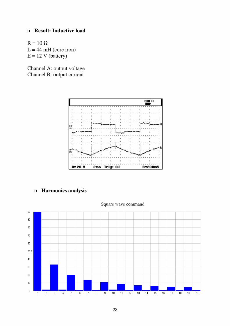
Result: Inductive load
R = 10 ΩL = 44 mH (core iron)E = 12 V (battery)
Channel A: output voltageChannel B: output current
Harmonics analysis
Square wave command

29
III. DELAYED COMMAND
The switching command of the second leg is delayed from the first leg by anangle called “d”.
d must satisfy d < π
when d = 60 °, third harmonic is vanished
The pulse width is 120° wide
Closed devices
PANEL B

30
Result: resistive load
R = 100 ΩE = 12 VD = 60°
Harmonics analysis
third harmonic is vanished
Delayed command d = 60°

31
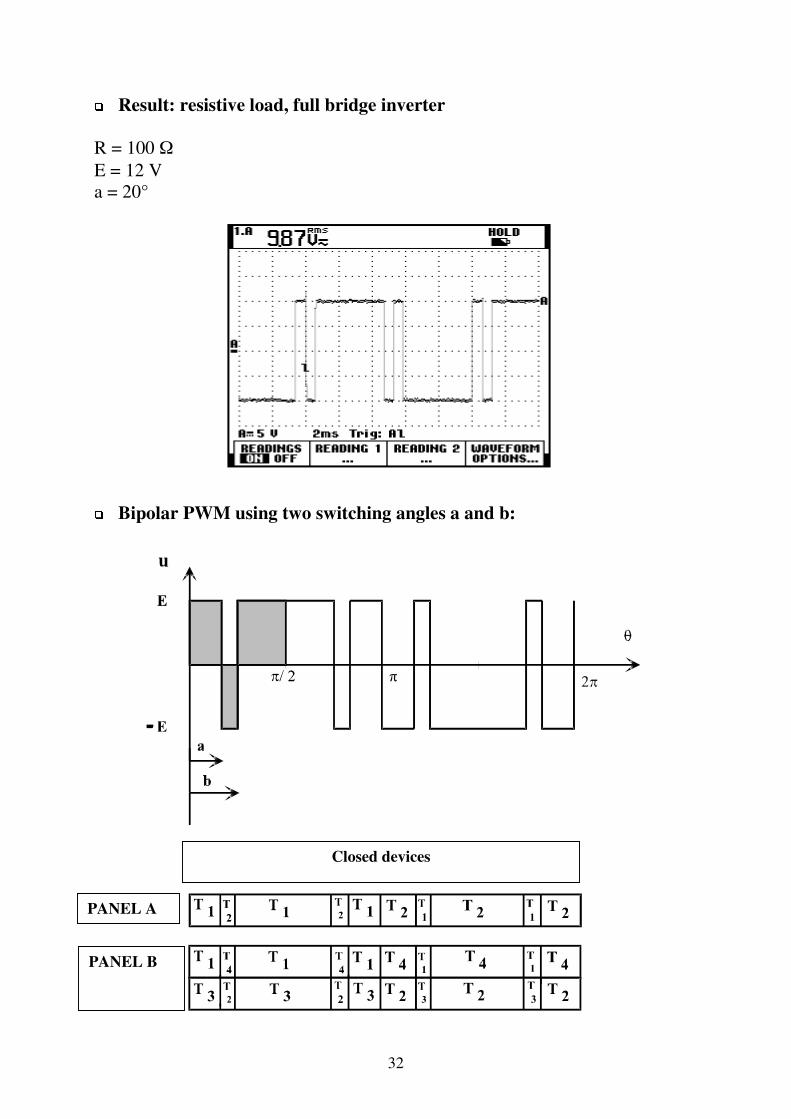
IV BIPOLAR PWM
PWM is a command technique that improves the quality of the outputwaveform. In this technique, harmonics are pushed to higher frequencies.Thus the cut-off frequency of the filter is increased. Hence the filtercomponents (ie L and C) size are reduced.
Moreover both frequency and amplitude can be independently controlled.
A PWM is basically obtained with a triangulation method or natural sampling:
Amplitude of the triangular wave (carrier) and sine wave(modulating) are compared to obtain PWM waveform. Simple analogcomparator can be used.
Bipolar PWM
Output voltage changes are from +E or –E
Switching angle: a
When a = 20°, third harmonic is vanishedTotal harmonic distorsion, THD is 54.14 %
Closed devices
PANEL A
PANEL B
32
Result: resistive load, full bridge inverter
R = 100 ΩE = 12 Va = 20°
Bipolar PWM using two switching angles a and b:
Closed devices
PANEL A
PANEL B

33
Third and fifth harmonics are vanished when a = 23.6 ° and b = 33.3 °(mathematical values)
THD is 64.85%
Result: resistive load
R = 100 ΩE = 12 Va = 24°b = 34°

34
V UNIPOLAR PWM
In this technique the output voltage changes are from –E to 0 and 0 to +E:-E; 0; +E
Therefore the magnitude of the harmonics are reduced by half. The outputwaveform presents twice as much notches meaning that the frequency of theharmonics doubled.
Switching angle a:
When a = 30° third harmonic is vanished
THD is 30.9%
Closed devices
PANEL B
35
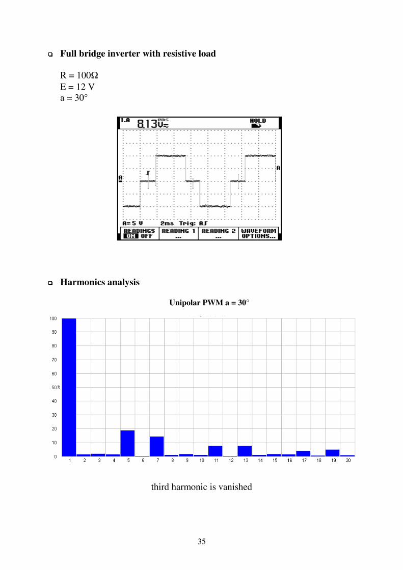
Full bridge inverter with resistive load
R = 100ΩE = 12 Va = 30°
Harmonics analysis
third harmonic is vanished
Unipolar PWM a = 30°

36
Switching angles a and b:
Third and fifth harmonics are vanished when a = 17.6° and b = 37.8°
THD is 60.7%
Parameters:
By default when 20 is pressed, a = 0° and b= 0°.b angle must be modified before a.
a and b must satisfy:
0 a b /2
Closed devices
PANEL B
37
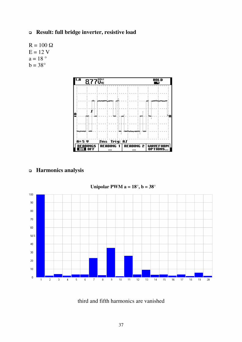
Result: full bridge inverter, resistive load
R = 100 ΩE = 12 Va = 18 °b = 38°
Harmonics analysis
third and fifth harmonics are vanished
Unipolar PWM a = 18°, b = 38°

38
Note: a and b values can be read directly on the screen of the scope.However cursors can be suitable if the scope is a digital one.

39
LABORATORY WORK
HALF BRIDGE VOLTAGE SOURCE INVERTER
PANEL A
40
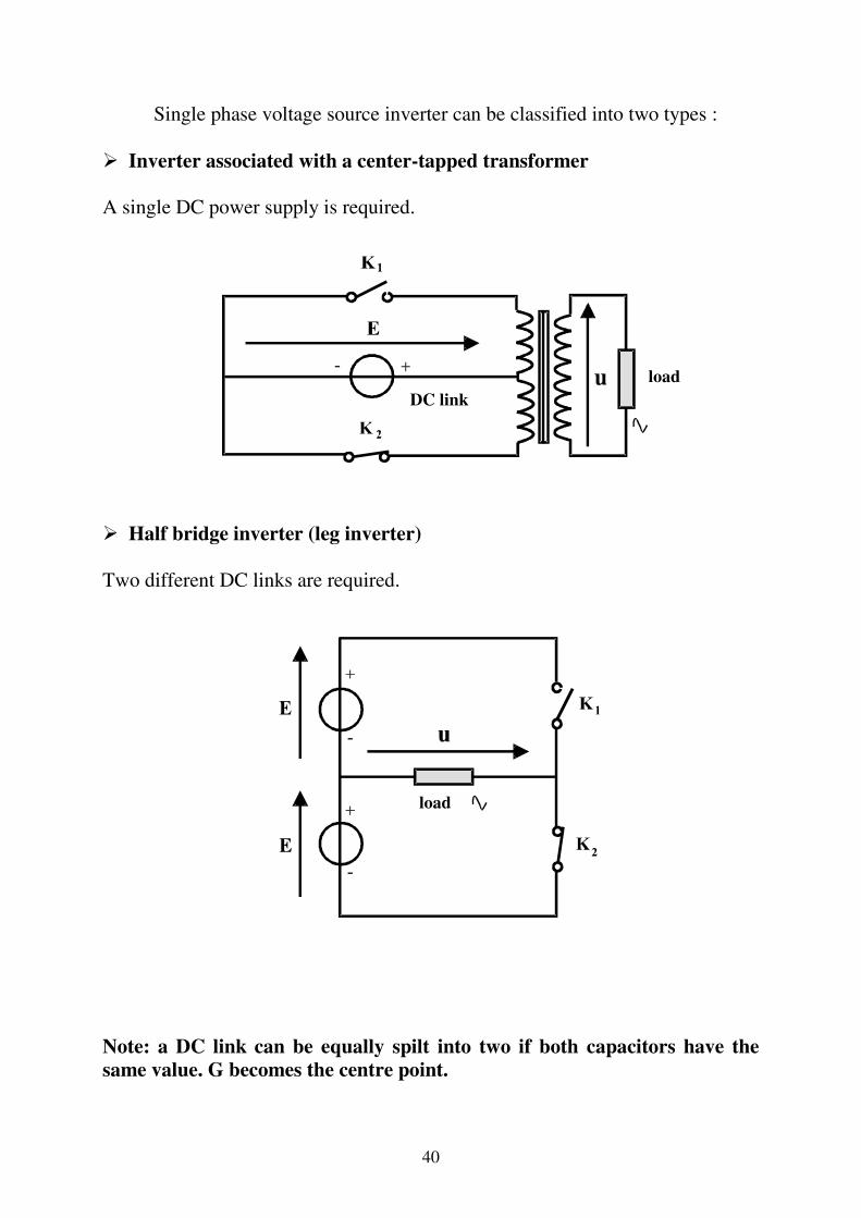
Single phase voltage source inverter can be classified into two types :
Inverter associated with a center-tapped transformer
A single DC power supply is required.
Half bridge inverter (leg inverter)
Two different DC links are required.
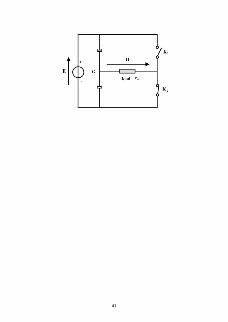
Note: a DC link can be equally spilt into two if both capacitors have thesame value. G becomes the centre point.
DC linkload
load
41
load
G

42
RESISTIVE LOAD
The Panel A is set, the bench is supplied (rear side)
Scheme :
DC link : DC power supply (IMAX = 3 A).Load :rheostat 10 Ω/5,7 A or 33 Ω/3,1 A.
Set up every components

43
A – Square wave command
I – Power switches
When the bench is turned on, square wave mode and 100 Hz outputfrequency are displayed..
1) Visualize and plot both T1 and T2 command signals respectively cm1 andcm2.
2) Measure and compare command signals frequency to the displayedfrequency.
3) Note that whatever the chosen frequency both signals remaincomplementary with each other.
II – Waveforms
Two strap wires are required, CT1 and CT2 respectively associated to T1 and T2.
Two strap wires are required, CD1 and CD2 respectively associated to D1 and D2.
The load is plugged. CT1 and CT2 are set..
The bench is supplied (+/- 15 V) Symmetric DC link is plugged.
Power is turned on, adjust the DC link up to 12 V.
DC link
M is grounded
E1 and E2 must have the same waveforms (both signals are superposed)

44
Visualize ig1 and ig2 with a current probe.
Inverter
S is grounded now.
1) Visualize simultaneously VDS1 and VDS2 (INV)
2) Visualize simultaneously iT1 and iT2, currents into T1 and T2.
3) CD1 is plugged. Visualize ID2 (current probe).
4) CD1 is removed. CD2 is plugged: visualize ID1.
Load
M is grounded
1) Visualize the output voltage
2) Visualize the output current
III -- Analysis
Both transistors are complementary as follows:
1) What about voltage losses due to power switches?
2) Deal with the inverter when:
closed evices
Panel A

45
E1 = u(t) + VDS1(t)
et where E1 = E2 = E
VDS2(t) = E2 + u(t)
3) Show that the “the inverter leg “ is a DC to AC waveform converter.
4) Could you expect the output current waveform?
IV -- Measurements
1) Fill the following cells:
LOAD ÛC
scopeUC
AC + DCCU
DC
ÎC IC CI
VALUES
2) Fill the following cells:
MOSFET transistorÛTinv ÎT IT TI
Values
V -- Spectrum analysis
E = 12 V; f = 100 Hz
The Fourier series of the output voltage is given as:
u(t) = ⎥⎦
⎤⎢⎣
⎡+ω+ω+ω
π...)t5sin(
5
1)t3sin(
3
1)tsin(
E4

46
1) Deal with the fact that only odd harmonics remain.
2) What about the mean value? Verify experimentally.
3) Visualize the output voltage spectrum.- deal with the number of harmonics- compare it with Fourier analysis
4) The fundamental is called u1f
- define u1f(t) as a function of E- give RMS expression U1f of u1f as a function of E.
Calculate U1f.- what kind of electronic filter can be used in order to select
fundamental part of the output signal?- What are the main disadvantages with square wave
command?

47
B Bipolar PWM
I – Power switches
Select bipolar PWM with 17 adjust parameters as follows : f = 200 Hz, a = 35 ° and b = 0 °."ENTER".
1) Compare cm1 and cm2.
2) Verify f and a with the scope.
3) Visualize and plot both T1 and T2 command signals (cm1 and cm2).
Adjust now f = 100 Hz, a = 30° and b = 45°
1) Verify f, a and b with the scope
2) Visualize and plot T1 and T2 command signals
3) What condition a and b must verify to reach bipolar PWM?
II -- Waveforms
Single angle PWM: E = 12V, f = 200 Hz, a = 35° and b = 0°
DC link
Visualize and plot ig1 and ig2 with a current probe
Inverter
1) Visualize and plot simultaneously VDS1 and VDS2
2) Visualize simultaneously iT1 and iT2, currents into T1 and T2.
48
Load
1) Visualize and plot the output voltage
2) Visualize and plot the output current
Repeat previous actions with the following parameters: E = 12V, f = 200 Hz,a = 30° and b = 45 °
III Analysis
Both transistors are complementary as follows:
Command switching
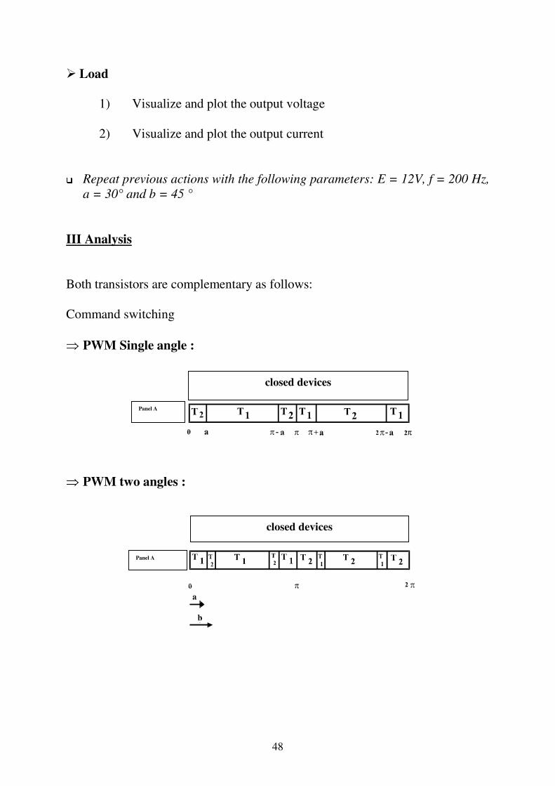
PWM Single angle :
PWM two angles :
closed devices
Panel A
closed devices
Panel A

49
IV Measurements
Fill the following cells :
LOAD ÛC
ScopeUC
AC + DCCU
DC
ÎC IC CI
VALUES
V – Spectrum analysis : E = 12 V and f = 200 Hz
single angle:
Fourier series of the output voltage is given as :
u(t) = ∑+∞
=+ ω+
0k1k2 t)1k2sin(b
where [ ]1a)1k2cos(2)1k2(
E4b 1k2 −+
+π=+
1) Check the mean value is zero whatever a
2) Compare analysis spectrum when:
a = 35 ° and a = 20b = 0° and b = 0°
- what about third harmonic?
- Give the first five harmonics of Fourier series of the output voltage forboth couple angles and compare with the spectrum analysis.

50
two angles:
Fourier series of the output voltage is given as :
u(t) = ∑+∞
=+ ω+
0k1k2 t)1k2sin(b
where [ ]b)1k2cos(2a)1k2cos(21)1k2(
E4b 1k2 +++−
+π=+
1) Compare analysis spectrum when:
a = 30 ° and a = 24°b = 45° and b = 34°
- what about third and fifth harmonics?
-Give the first five harmonics of Fourier series of the output voltage forboth couple angles and compare with the spectrum analysis.
- what kind of electronics filter ca be used in order to select thefundamental of the output signal?
2) Compare square wave and bipolar PWM commands.

51
INDUCTIVE LOAD
Panel A is set, the bench is supplied (rear side)
Scheme :
DC link : DC power supply, current reversible (IMAX = 3 A).
Load :rheostat 10 Ω/5,7 A or 33 Ω/3,1 A in series with an iron core coil L (10Ω/ 0.1 H – 1.4 H)
Set up every components

52
R, L Load is connected
All strap wires are plugged
DC power supplies are connected, E1 = E2 = E = 24 V
The bench is turned on
A – Square wave command
I – Waveforms
L = 0,2 H, and f = 50 Hz.
DC link
Visualize and plot ig1(t) and ig2(t)
Inverter
1) Visualize simultaneously VDS1 and VDS2
2) Visualize simultaneously VD1 and VD2
3) Visualize and plot simultaneously iT1 and iT2, currents into T1 and T2
4) Visualize and plot iD1 and iD2.
Load
1) Visualize an plot output voltage
2) Visualize and plot output current.

53
II – Analysis
Both transistors are complementary as follows :
1) Is the output voltage modified by the coil ?
2) What about voltage losses due to power switches?
3) Compare this output voltage with the one obtained with the square wavecommand.
4) Explain the behaviour of the circuit;
- give closed devices for each switching step- give net power sign for each switching step
III – Measurements
Fill the following cells :
LOAD ÛC
scopeUC
AC +DC
CU
DCÎC IC CI
VALUE
closed devices
Panel A

54
IV – Spectrum analysis
Fourier series of output voltage is given as :
u(t) = ⎥⎦
⎤⎢⎣
⎡+ω+ω+ω
π...)t5sin(
5
1)t3sin(
3
1)tsin(
E4
1) Visualize and plot output current (current probe)
2) Give harmonics decomposition of output current (from u(t)). Whatabout harmonics level?
3) What kind of load R, L association can simulate?
4) Give fundamental expression i1f(t) of i(t) as a function of E, L, ω andphaseshift.
5) Then give RMS expression I1f of i1f(t). Compare it with spectrumanalysis.

55
B – Bipolar PWM
Select bipolar PM mode with 17
Adjust parameters as follows: f = 50 Hz, a = 35° and b = 0°
Enter
Single angle
E = 12 V, f = 50 Hz, a = 20° and b = 0°
1) Visualize and plot command signals, output signals and realizespectrum analysis.
2) Plot switching command diagrams and explain the behaviour of suchconfiguration.
Two angles
Repeat previous actions with following parameters: E = 24 V, f = 50 Hz, a = 24°and b =34 °
Note:give closed devices for each switching stepgive net power sign for each switching step

56
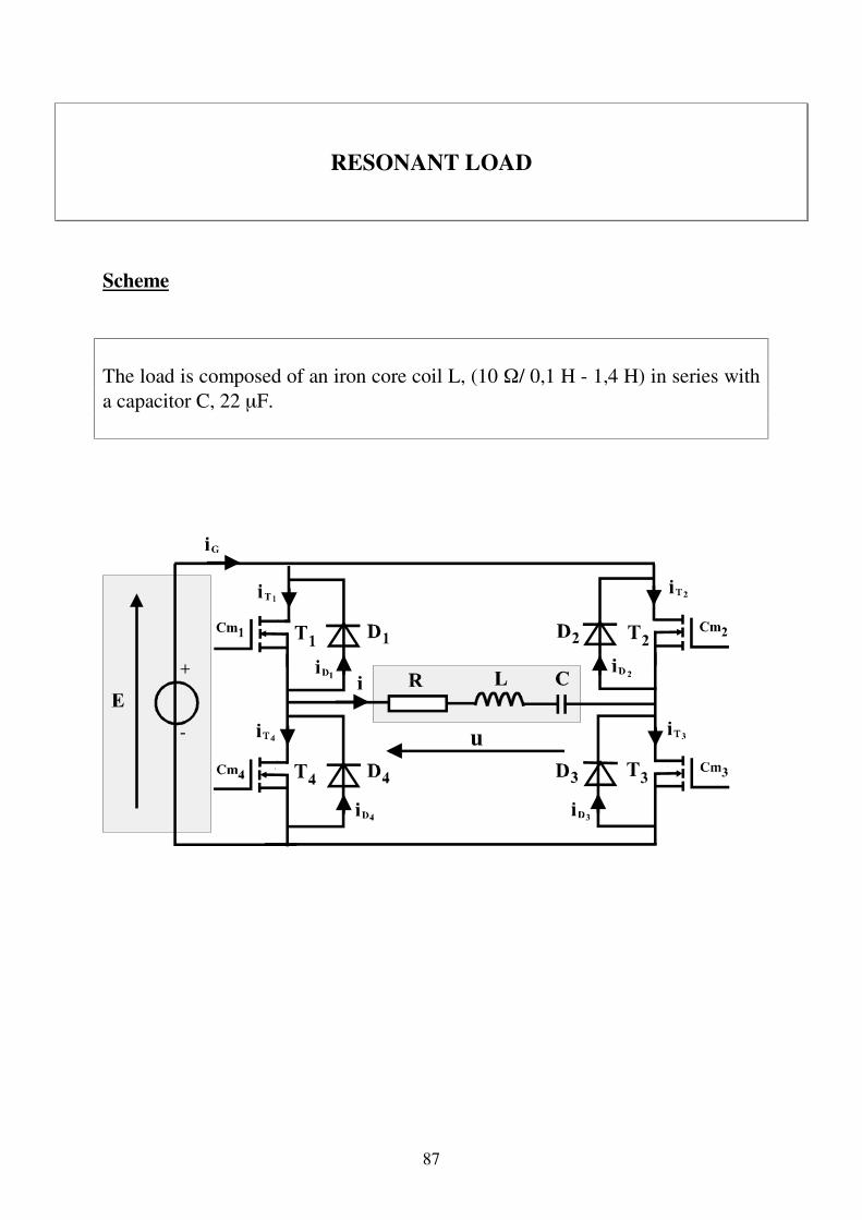
RESONANT LOAD
Scheme
DC link : DC power supply, current reversible (IMAX = 3 A).
Load :rheostat 10 Ω/5,7 A or 33 Ω/3,1 A in series with an iron core coil L (10Ω/ 0.1 H – 1.4 H) and a capacitor C (22 µF)

57
A – Square wave command
I – Power switches
Select square wave command
Adjust f = 50 Hz
Enter
1) Visualize simultaneously command signals of T1 and T2
2) Plot command signals diagram and give closed devices
R, L, C Load is connected
All strap wires are plugged
DC power supplies are connected, E1 = E2 = E = 12 V
The bench is turned on
II -- Waveforms
DC link
Visualize and plot ig1(t) and ig2(t)
Inverter
1) Visualize simultaneously VDS1 and VDS2
2) Visualize simultaneously VD1 and VD2
3) Visualize and plot simultaneously iT1 and iT2, currents into T1 and T2

58
4) Visualize and plot iD1 and iD2.
Load
1) Visualize an plot output voltage
2) Visualize and plot output current.
II – Analysis
Both transistors are complementary as follows :
1) Deal with R, L,C load about output current and command signalswaveforms.
2) Adjust L to obtain no phaseshift between output voltage and outputcurrent. Output current should become sine wave or quasi sine wave.What is that phenomenon?
3) Check output frequency fo and compare it with theoretical expression.
4) Deal with f < fo and f > fo
Note:give closed devices for each switching stepgive net power sign for each switching step
closed devices
Panel A

59
III – Measurements
Fill the following cells :
LOADf = fo
ÛC
scopeUC
AC +DC
CU
DCÎC IC CI
VALUE
IV – Spectrum analysis
f = 210 Hz
C = 2.2 µF, L = 0.25 H (resonance is reached)
1) Give quality factor Q = Lωo / RT , where RT is the total resistance of thecircuit.
2) Give value of the load when resonance is reached. What about the loadimpedance before and after resonance?
3) Fourier series of output voltage is given as:
u(t) = ⎥⎦
⎤⎢⎣
⎡+ω+ω+ω
π...)t5sin(
5
1)t3sin(
3
1)tsin(
E4
If output frequency matches resonance frequency of the RLC load, thelatter behaves as a selecting filter. Harmonics are thus vanished.
Note: when output frequency is such as fo / k, the kth harmonic will beconsidered as a fundamental.

60
Fill the following cells:
k (rank) 1 3 5 7
f (Hz)
k.f (Hz) f0 = 210 Hz
I (mA)
I theoretical
Where I = (4E/RT.k.π)

61
B – Bipolar PWM
Single angle mode
Select bipolar PM mode with 17
Adjust parameters as follows: f = 210 Hz, a = 20° and b = 0°
Enter
Fill the following cells :
k (rank) 1 3 5 7
f (Hz)
kf (Hz) f0 = 210 Hz
Two angles mode
Adjust parameters as follows: f = 210 Hz, a = 24 ° and b = 34 °
Enter
Fill the following cells:
k (rank) 1 3 5 7
f (Hz)
kf (Hz) f0 = 210 Hz

62
LABORATORY WORK
FULL BRIDGE VOLTAGE SOURCE INVERTER
PANEL B

63
RESISTIVE LOAD
The Panel B is set, the bench is supplied (rear side)
Scheme
DC link: DC power supply, Imax = 3 ALoad: rheostat R : 10 Ω/5,7 A or 33 Ω/3,1 A.

64
A – Square wave command
I – Power switches
When the bench is turned on, square wave mode and 100 Hz outputfrequency are displayed.
1) Visualize and plot T1 and T4 command signals, respectively cm1 and cm4.
2) Measure and compare the command signal frequency to the displayed value.
3) Note that whatever the chosen frequency both signals remain complementarywith each other.
4) Visualize and plot T2 and T3 command signals, respectively cm2 and cm3.Both signals must remain complementary.
II – Waveforms
Four strap wires are required. CT1, CT2, CT3 and CT4 respectively associated toT1, T2, T3 and T4.
The load is plugged, all strap wires are set.
The bench is supplied (+ / - 15 V). DC link is plugged.
Power is turned on, adjust DC link up to 12 V.
DC link
Visualize and plot the source output current, ig(t).
Inverter

65
A is grounded
1) Visualize simultaneously VDS1 and VDS4 (INV)
B is grounded
2) Visualize simultaneously VDS2 and VDS3 (INV)
3) Visualize iT1, iT2, iT3 and iT4 currents into T1, T2, T3 and T4.
Load
B is grounded
1) Visualize the output voltage
2) Visualize the output current.
III – Analysis
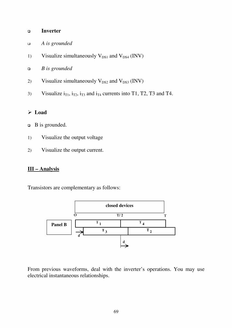
Transistors are complementary as follows:
1) From previous waveforms, deal with the inverter’s operations. You mayuse electrical instantaneous relationships.
2) Could you expect such output waveform?
closed devices
Panel B

66
IV – Measurements
1) Fill the following cells:
LOAD ÛC
ScopeUC
AC + DCCU
DC
ÎC IC CI
VALUES
2) Fill the following cells:
MOSFET ÛTinv ÎT IT TI
VALUES
V – Spectrum analysis
E = 12 V, f = 100 Hz
Fourier series of the output voltage is given as:
u(t) = ⎥⎦
⎤⎢⎣
⎡+ω+ω+ω
π...)t5sin(
5
1)t3sin(
3
1)tsin(
E4
1) What about the mean value?
2) Visualize the output voltage spectrum- deal with the number of harmonics- compare it with Fourier analysis

67
3) The fundamental is called u1f(t).- define u1(t) as a function of E- Give RMS expression U1f of u1f as a function of E. Calculate
U1f.- What kind of electronic filter can be used in order to keep
fundamental part of the output signal?- What are the main disadvantages with square wave command?

68
B – Delayed command
I – Power switches
Select delayed PWM with 20.
Adjust parameters as follows: f = 250 Hz, d = 40 °
Enter
1) Visualize every command signals, cm1, cm2, cm3 and cm4. Signals belongingto the same leg must be complementary and delayed (angle d).
2) Plot cm1, cm2, cm3 and cm4.
3) Adjust d from 0° to highest value. Which values must be verified by d inorder to reach delayed command?
II – Waveforms
Four strap wires are required. CT1, CT2, CT3 and CT4 respectively associated to T1,T2, T3 and T4.
The load is plugged, all strap wires are set.
The bench is supplied (+ / - 15 V). DC link is plugged.
Power is turned on, adjust DC link up to 12 V.
DC link
Visualize and plot the source output current, ig(t).
69
Inverter
A is grounded
1) Visualize simultaneously VDS1 and VDS4 (INV)
B is grounded
2) Visualize simultaneously VDS2 and VDS3 (INV)
3) Visualize iT1, iT2, iT3 and iT4 currents into T1, T2, T3 and T4.
Load
B is grounded.
1) Visualize the output voltage
2) Visualize the output current.
III – Analysis
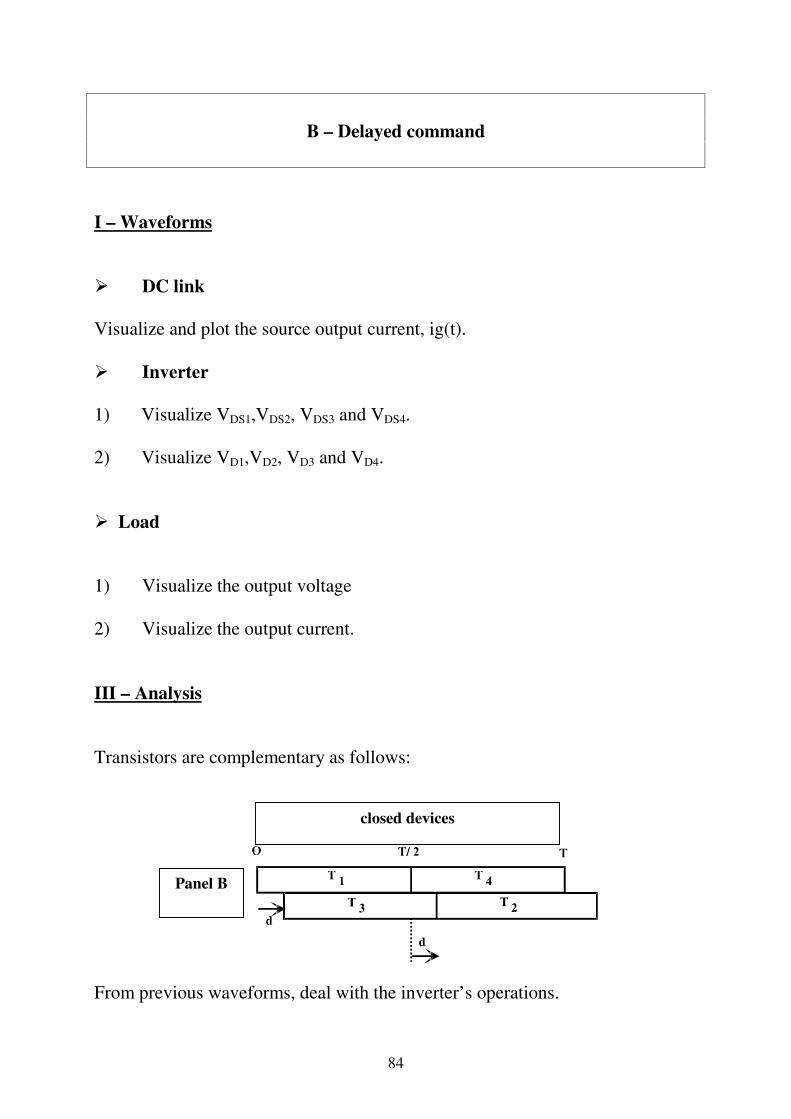
Transistors are complementary as follows:
From previous waveforms, deal with the inverter’s operations. You may useelectrical instantaneous relationships.
closed devices
Panel B

70
IV – Measurements
Fill the following cells:
LOAD ÛC
ScopeUC
AC + DCCU
DC
ÎC IC CI
VALUES
V – Spectrum analysis
E = 12 V
Fourier series of the output voltage is given as:
u(t) = ∑+∞
=+ ω+
0k1k2 t)1k2sin(b
where [ ]d)1k2cos(1)1k2(
E2b 1k2 ++
+π=+
1) What about the mean value?
2) Output voltage spectrum, E= 12 V and f = 250 Hz
Adjust d up to 40°
1) Visualize the output voltage spectrum
Adjust d up to 60°

71
2) Visualize the output voltage spectrum. Note that the thirdharmonic is vanished.
3) Derive first five harmonics when d is 40° and 60°.- derive u1f((t) as a function of E- thus derive U1f as a function of E- calculate E
4) What kind of electronic filter can be used in order to keep thefundamental part of u(t)?
Compare square wave command with delayed command.

72
C – Bipolar PWM
I – Power switches
Select Bipolar PWM with 20
Adjust parameters as follows: f = 150 Hz, a = 40° and b = 0°
Enter
1) Measure the output frequency and visualize cm1, cm2, cm3, cm4, and a.
Adjust new parameters as follows: f = 150 Hz, a = 30° and b = 45°
2) Measure the output frequency and visualize cm1, cm2, cm3, a and b.
3) Which values must verify a and b in order to reach bipolar PWM?
II – Waveforms
1. Single angle PWM: E = 12V, f = 150 Hz, a = 40° and b = 0°
2. Two angles PWM: E = 12V, f = 150 Hz, a = 30° and b = 45°
DC link
Visualize and plot the source output current, ig(t).
Inverter
1) Visualize simultaneously VDS1 and VDS4 (INV)
2) Visualize simultaneously VDS2 and VDS3 (INV)
3) Visualize iT1, iT2, iT3 and iT4 currents into T1, T2, T3 and T4.

73
Load
1) Visualize the output voltage
2) Visualize the output current.
III – Analysis
Transistors are complementary as follows:
From previous waveforms, deal with the inverter’s operations.
closed devices
Panel B
closed devices
Panel B

74
IV – Measurements
Fill the following cells:
LOAD ÛC
ScopeUC
AC + DCCU
DC
ÎC IC CI
VALUES
V – Spectrum analysis E = 12 V
Single angle: E = 12V, f = 150 Hz
Fourier series of the output voltage is given as:
u(t) = ∑+∞
=+ ω+
0k1k2 t)1k2sin(b
where [ ]1a)1k2cos(2)1k2(
E4b 1k2 −+
+π=+
1) What about the mean value?
2) Output voltage spectrum
a) Adjust a up to 35°Visualize the output voltage spectrum
b) Adjust a up to 20°Visualize the output voltage spectrum. Verify that the third
harmonic is vanished.

75
c) Derive the first five harmonics of the output voltage.
Two angles: E = 12V and f = 250 Hz
Fourier series of the output voltage is given as:
u(t) = ∑+∞
=+ ω+
0k1k2 t)1k2sin(b
where [ ]b)1k2cos(2a)1k2cos(21)1k2(
E4b 1k2 +++−
+π=+
a) Same questions with the following parameters:
a = 30° a = 24°b = 45° b = 34°
b) Derive first five harmonics
c) What kind of electronic filter can be used in order tokeep the fundamental part of u(t)?
Compare square wave command with bipolar PWM command.

76
D – Unipolar PWM
I – Power switches
Select Bipolar PWM with 20
Adjust parameters as follows: f = 150 Hz, a = 40° and b = 0°
Enter
1) Measure the output frequency and visualize cm1, cm2, cm3, cm4, and a.
Adjust new parameters as follows: f = 200 Hz, a = 30° and b = 50°
2) Measure the output frequency and visualize cm1, cm2, cm3, a and b.
3) Which values must verify a and b in order to reach bipolar PWM?
II – Waveforms
⇒Single angle PWM: E = 12V, f = 150 Hz, a = 40° and b = 0°
⇒Two angles PWPM: E = 12V, f = 150 Hz, a = 25° and b = 50°
DC link
Visualize and plot the source output current, ig(t).
Inverter
1) Visualize simultaneously VDS1 and VDS4 (INV)
2) Visualize simultaneously VDS2 and VDS3 (INV)
3) Visualize iT1, iT2, iT3 and iT4 currents into T1, T2, T3 and T4.

77
Load
1) Visualize the output voltage
2) Visualize the output current.
III – Analysis
Transistors are complementary as follows:
From previous waveforms, deal with the inverter’s operations.
IV – Measurements
Fill the following cells:
LOAD ÛC
ScopeUC
AC + DCCU
DC
ÎC IC CI
VALUES
V – Spectrum analysis E = 12 V
Single angle: E = 12V, f = 150 Hz
Fourier series of the output voltage is given as:
closed devices
Panel B

78
u(t) = ∑+∞
=+ ω+
0k1k2 t)1k2sin(b
where [ ]a)1k2cos()1k2(
E4b 1k2 +
+π=+
1) What about the mean value?
2) Output voltage spectrum
a) Adjust a up to 40°Visualize the output voltage spectrum
b) Adjust a up to 30°Visualize the output voltage spectrum. Verify that the third
harmonic is vanished
c) Derive the first five harmonics of the output voltage.
Two angles: E = 12V and f = 250 Hz
Fourier series of the output voltage is given as:
u(t) = ∑+∞
=+ ω+
0k1k2 t)1k2sin(b
where [ ]b)1k2cos(a)1k2cos(1)1k2(
E4b 1k2 +++−
+π=+
a) Same questions with the following parameters:
a = 25° a = 18°b = 50° b = 38°

79
b) Derive first five harmonics
d) What kind of electronic filter can be used in order tokeep the fundamental part of u(t)?
Compare square wave command with unipolar PWM command.

80
INDUCTIVE LOAD
The Panel B is set, the bench is supplied (rear side)
Scheme
DC link: DC power supply, Imax = 3 ALoad: rheostat R : 10 Ω/5,7 A or 33 Ω/3,1 A in series with an iron core coil (10Ω / 0.1 H – 1.4 H)
The R, L load is plugged and all strap wires are set.
The DC link is on
The bench is turned on, adjust f up to 50 Hz and E up to 24 V

81
A – Square wave command
I – Waveforms
DC link
Visualize and plot the source output current, ig(t).
Inverter
1) Visualize and plot VDS1, VDS2, VDS3 and VDS4
2) Visualize and plot VD1, VD2, VD3 and VD4
The following table may be useful:
point C point D
NOT INV INV NOT INV INV
A is grounded VDS1 VD1 VD4 VDS4
B is grounded VDS2 VD2 VD3 VDS3
3) Visualize iT1, iT2, iT3 and iT4 currents into T1, T2, T3 and T4.
4) Visualize iD1, iD2, iD3 and iD4 currents into D1, D2, D3 and D4.
Load
1) Visualize and plot the output voltage
2) Visualize and plot the output current

82
II -- Analysis
Both transistors are complementary as follows:
1) The output voltage is not altered by the iron core coil. Explain the reasonwhy? What about voltage losses due to rectifiers?
2) Compare currents waveforms between inductive and resistive load.
3) From previous waveforms, deal with the inverter’s behaviour.
Picture equivalent circuit for each switching step including current’s path.
Note:give closed devices for each switching stepgive net power sign for each switching step
III – Measurements
Fill the following cells:
LOAD ÛC
ScopeUC
AC + DCCU
DC
ÎC IC CI
VALUES
closed devices
Panel B

83
IV – Spectrum analysis " E = 24 V et f = 50 Hz
Fourier series of the output voltage is given as :
u(t) = ⎥⎦
⎤⎢⎣
⎡+ω+ω+ω
π...)t5sin(
5
1)t3sin(
3
1)tsin(
E4
1) Visualize and plot the spectrum analysis of the output current
2) Note that the harmonics level is reduced. Explain thus the influence of thecoil. Which consequences may be induced when the load is an ac motor?
3) The fundamental of i1(t) is called i1f(t).- define i1(t) as a function of E, L,ω and phaseshift- Give RMS expression I1f of i1f . Calculate I1f.
84
B – Delayed command
I – Waveforms
DC link
Visualize and plot the source output current, ig(t).
Inverter
1) Visualize VDS1,VDS2, VDS3 and VDS4.
2) Visualize VD1,VD2, VD3 and VD4.
Load
1) Visualize the output voltage
2) Visualize the output current.
III – Analysis
Transistors are complementary as follows:
From previous waveforms, deal with the inverter’s operations.
closed devices
Panel B

85
C – Bipolar and Unipolar PWM commands
I – Bipolar PWM
Select bipolar mode with 20
Adjust the following parameters:
⇒Single angle : E = 24 V, f = 50 Hz, a= 20° and b = 0°
Two angles : E = 24 V, f = 50 Hz, a = 24° and b = 34°
Enter
1) Visualize both command signals and output voltage.
Note:give closed devices for each switching stepgive net power sign for each switching step
2) Visualize the output voltage spectrum analysis.
II – Unipolar PWM
Select bipolar mode with 20
Adjust the following parameters:
⇒Single angle : E = 24 V, f = 50 Hz, a= 40° and b = 0°
Two angles : E = 24 V, f = 50 Hz, a = 18° and b = 38°
Enter
1) Visualize both command signals and output voltage.

86
Note:give closed devices for each switching stepgive net power sign for each switching step
2) Visualize the output voltage spectrum analysis.
87
RESONANT LOAD
Scheme
The load is composed of an iron core coil L, (10 Ω/ 0,1 H - 1,4 H) in series witha capacitor C, 22 µF.

88
A – Square wave command
I – Waveforms
DC link
Visualize and plot the source output current, ig(t).
Inverter
1) Visualize and plot VDS1, VDS2, VDS3 and VDS4
2) Visualize and plot VD1, VD2, VD3 and VD4
The following table may be useful:
point C point D
NON INV INV NON INV INV
A is grounded VDS1 VD1 VD4 VDS4
B is grounded VDS2 VD2 VD3 VDs3
3) Visualize iT1, iT2, iT3 and iT4 currents into T1, T2, T3 and T4.
4) Visualize iD1, iD2, iD3 and iD4 currents into D1, D2, D3 and D4.
Load
1) Visualize and plot the output voltage
2) Visualize and plot the output current

89
II -- Analysis
Both transistors are complementary as follows:
5) Deal with the R, L,C load about the output current and command signalswaveforms.
6) Adjust L to obtain no phaseshift between output voltage and outputcurrent. Output current should become sine wave or quasi sine wave.What is that phenomenon?
7) Measure output current frequency fo. Derive fo.
8) Deal with f < fo and f > fo
Note:give closed devices for each switching stepgive net power sign for each switching step
III – Measurements
Fill the following cells:
LOADf = fo
ÛC
ScopeUC
AC + DCCU
DC
ÎC IC CI
VALUES
closed devices
Panel B

90
IV – Spectrum analysis " E = 24 V et f = 50 Hz
f = 210 Hz
C = 2.2 µF, L = 0.25 H (resonance is reached)
1) Give the quality factor Q = Lωo / RT , where RT is the total resistance ofthe circuit.
2) Give the value of the load when resonance is reached. What about theload impedance before and after resonance?
3) The Fourier series of the output voltage is given as:
u(t) = ⎥⎦
⎤⎢⎣
⎡+ω+ω+ω
π...)t5sin(
5
1)t3sin(
3
1)tsin(
E4
If the output frequency matches resonance frequency of the RLC load, thelatter behaves as a selecting filter. Harmonics are thus vanished.
Note: when the output frequency is such as fo / k, the kth harmonic willbe considered as a fundamental.
Fill the following cells:
k (rank) 1 3 5 7
f (Hz)
k.f (Hz) f0 = 210 Hz
I (mA)
I(theoretical)
Where I = (4E/RT.k.π)

91
B – PWM command
Single angle bipolar PWM
Select bipolar mode with 20 Adjust parameters as follows: f = 210 Hz, a = 20° and b = 0° Enter
Fill the following cells:
k (rank) 1 3 5 7
f (Hz)
k.f (Hz) f0 = 210 Hz
Two angles bipolar PWM
Adjust parameters as follows : f = 210 Hz, a = 24 ° and b = 34 °. Enter
Fill the following cell:
k (rank) 1 3 5 7
f (Hz)
k.f (Hz) f0 = 210 Hz

92
The CO 200 bench is a pedagogical support with which the lecturer is able
to introduce practical applications like induction heating, emergency power
supply or motor drive.
The following applications are dedicated to enhance the general
knowledge of students.
Induction heating
Emergency power supply
Induction motor speed control

93
INDUCTION HEATING
I – Introduction
Induction heating can be used in a kitchen. Nowadays electrical or gas
cookers can be replaced by induction cooker:
A voltage source inverter supplies the primary windings of a
transformer which generates a variable magnetic field. Field lines are
caught by metallic receptacle (pan, sauce pan…). An emf appears and, as
the receptacle is shorted-circuit, eddy currents circulate into. This makes
the metallic receptacle to get warmer because of Joules’ effect. The pan acts
as the secondary windings of the transformer.
inverter
electromagneticfield
primary
inductioncoil
secondary
cooker
94
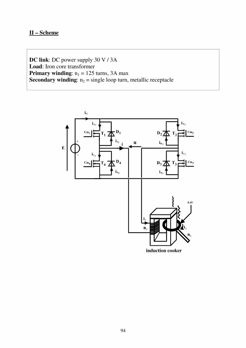
II – Scheme
DC link: DC power supply 30 V / 3ALoad: Iron core transformerPrimary winding: n1 = 125 turns, 3A maxSecondary winding: n2 = single loop turn, metallic receptacle
induction cooker

95
B – Panel is placed, the bench is supplied (rear side)
Select square wave command pressing 20.
Adjust f to 50 Hz
Enter
Set DC link up to 30 V
Put water into metallic loop. Switch the bench on.
CAUTION : metallic loop may bevery hot

96
III – Experiment
1) Is the transformer free, on load or shorted-ciruit?
2) Evaluate eddy currents with a current crowbar (MS 200 – MS 220)
3) Why does secondary current decrease while loop gets warmer?
4) What kind of energy losses do appear? (Joule, Hysteresis, eddycurrents…)
a) Fill the following cells:
E (V) U1 (V) I1 (A) P1 (W) Cos ϕ1 I2 (A) m U2 (V) P2 (W) η
10
20
30
40
50
Where cosϕ: power factorm : transformation ratioη : efficiency
b) plot P1 = f(E) and η = f(E)
c) Why do we use a step-up transformer? Show that a 500winding coil is enough to supply the induction cookerfrom mains (230 V/ 50 Hz)?

97
d) How does an induction cooker work?
e) Deal with the resistance of the secondary
5) Lets see how does the induction cooker work as a function of the output frequency.
Fill the following cells:
f (Hz) 0 50 100 150 200 250
I2 (A)
P (W)
η
6) Deal with your results.
7) Use delayed or PWM command. Compare both commands (delay angle, aor b angles…)
8) Give the electrical model for the induction cooker:
a) How can we obtain sine wave current?(electronic component).
b) What is this physical phenomenon?

98
EMERGENCY POWER SUPPLY
I – Introduction
Voltage source inverter can be used as emergency power supply in many
fields like computer systems. If a default appears on the line, the inverter is
designed to supply computers or network systems with 230 V / 50 Hz for
example. Then work in progress or data can be saved.
II – Scheme
Inverter bench: CO-120 used as emergency power supplyDC link: batteries 24 VConverter bench: CO-100 used as chargerLoad: 24 V / 40 W bulb
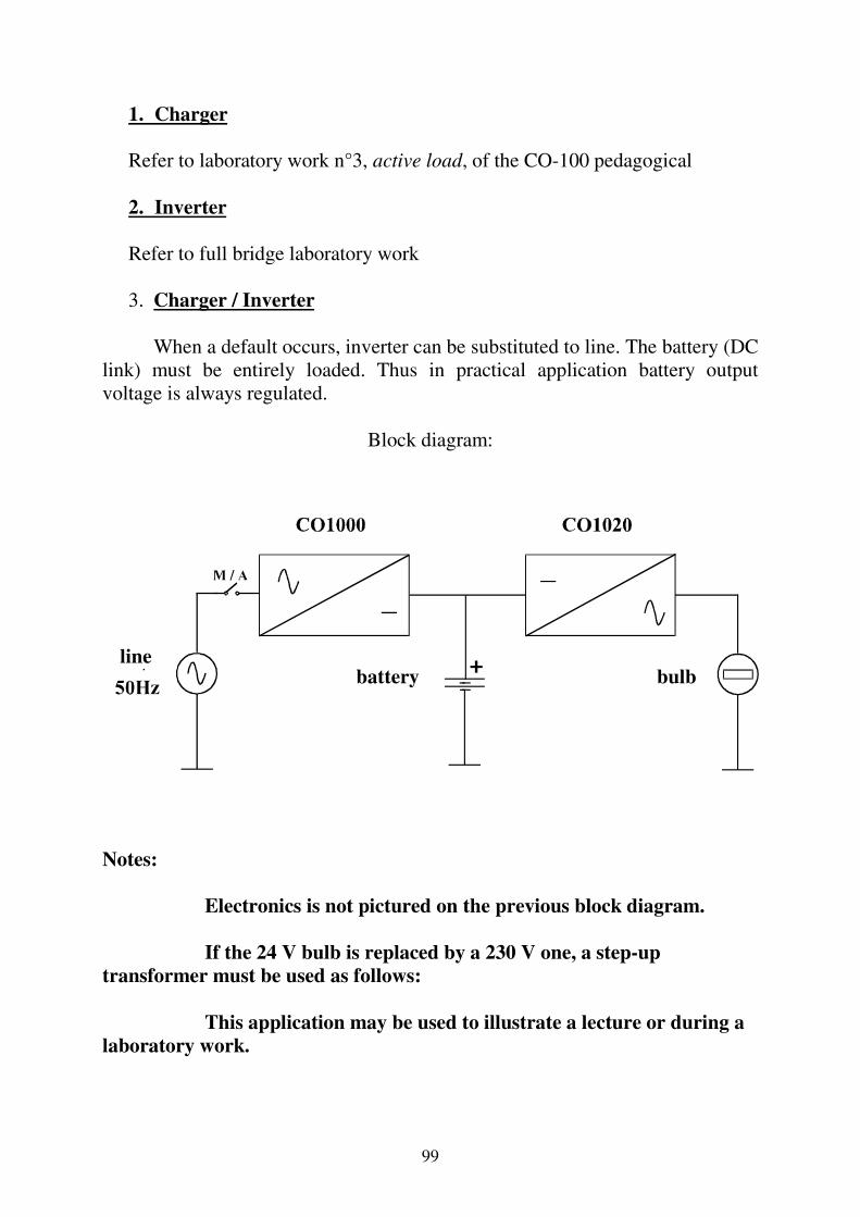
99
1. Charger
Refer to laboratory work n°3, active load, of the CO-100 pedagogical
2. Inverter
Refer to full bridge laboratory work
3. Charger / Inverter
When a default occurs, inverter can be substituted to line. The battery (DClink) must be entirely loaded. Thus in practical application battery outputvoltage is always regulated.
Block diagram:
Notes:
Electronics is not pictured on the previous block diagram.
If the 24 V bulb is replaced by a 230 V one, a step-uptransformer must be used as follows:
This application may be used to illustrate a lecture or during alaboratory work.
linebattery bulb
100
101
INDUCTION MOTOR DRIVE SYSTEM
I -- Introduction
Induction motors presents several advantages;
Robust, no brushesHigh power/weight ratio compared to DC motorEasy to manufacture
However it is essentially a fixed-speed machine. Its speed is determinedby the supply frequency. Thus to vary its speed, a variable frequency supply isneeded.
Induction motor is present in many applications like conveyer line drives,traction, electric vehicles, elevators… any industrial process that requiresvariable speed operation.
For variable speed operation, the supply is an inverter. The frequency ofthe fundamental AC output voltage will set the speed of induction motor.
The inverter output frequency must be kept close to the required motorspeed. This is necessary as the induction motor operates under low slipconditions.
However in order to maintain constant torque, the slip frequency must bemaintained over the range of supply frequencies.
When maximal motor flux is reached, maximum torque is obtained and,voltage to frequency ratio is kept constant. Constant Voltz/Herzt operation isused. The motor is operated at rated slip at all supply frequencies. Hence aconstant torque area is obtained as a function of speed.
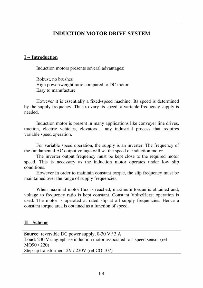
II – Scheme
Source: reversible DC power supply, 0-30 V / 3 ALoad: 230 V singlephase induction motor associated to a speed sensor (refMO90 / 220)Step-up transformer 12V / 230V (ref CO-107)

102
Note: the step-up transformer becomes useless according to the induction
motor voltage supply.
Set the Panel B and switch the bench on (rear side).
Set every components and select square wave command with 20.
Adjust the frequency up to 50 Hz
Enter
Set the DC source up to 12 V.
III – Experiment
1) Let’s consider the secondary winding of the transformer
speed

103
a) Visualize the secondary voltage uM, use a step down probe.b) Measure both frequency and RMS value of uM.
2) Speed control:
a. Fill the following cells:
f (Hz) 0 30 50 80 100 150
n (rpm)speed
b. At which frequency does the motor stop? Increase thus the DCsource level.
c. Deal with your results. Plot P = f(E) and η = f(E).
3) Replace the AC motor by a series one and repeat the previousactions.


CO
1020
-GB-
08-2
005