Embed Size (px)
Citation preview

User’s Manual
Version 1.0, 2005 Single Board Computer 3301390

Copyrights This manual is copyrighted and all rights are reserved. It does not allow any non authorization in copied, photocopied, translated or reproduced to any electronic or machine readable form in whole or in part without prior written consent from the manufacturer. In general, the manufacturer will not be liable for any direct, indirect, special, incidental or consequential damages arising from the use of inability to use the product or documentation, even if advised of the possibility of such damages. The manufacturer keeps the rights in the subject to change the contents of this manual without prior notices in order to improve the function design, performance, quality and reliability. The author assumes no responsibility for any errors or omissions, which may appear in this manual, nor does it make a commitment to update the information contained herein. Trademarks Intel is a registered trademark of Intel Corporation. Award is a registered trademark of Award Software, Inc. All other trademarks, products and or product's name mentioned herein are mentioned for identification purposes only, and may be trademarks and/or registered trademarks of their respective companies or owners.

Preface
Table of Contents
How to Use This Manual
Chapter 1 System Overview.......................................................................................................1-1
1.1 Introduction.................................................................................................................................. 1-11.2 Check List ..................................................................................................................................... 1-31.3 Product Specification .................................................................................................................. 1-3
1.3.1 Mechanical Drawing ......................................................................................................... 1-61.4 System Architecture .................................................................................................................... 1-7
Chapter 2 Hardware Configuration ........................................................................................... 2-1
2.1 Jumper Setting ............................................................................................................................. 2-12.2 Connector Allocation .................................................................................................................. 2-4
Chapter 3 System Installation.................................................................................................... 3-1
3.1 Pentium M Processor .................................................................................................................. 3-13.2 Main Memory .............................................................................................................................. 3-33.3 Installing the Single Board Computer ...................................................................................... 3-3
3.3.1 Chipset Component Driver.............................................................................................. 3-53.3.2 Intel Integrated Graphics GMCH Chip .......................................................................... 3-53.3.3 On-board Gigabit Ethernet Controller ........................................................................... 3-63.3.4 On-board AC-97 Audio Device ....................................................................................... 3-6
3.4 Clear CMOS Operation............................................................................................................... 3-73.5 WDT Function.............................................................................................................................. 3-73.6 GPIO .............................................................................................................................................. 3-9
Chapter 4 BIOS Setup Information............................................................................................ 4-1
4.1 Entering Setup.............................................................................................................................. 4-14.2 Main Menu ................................................................................................................................... 4-24.3 Standard CMOS Setup Menu .................................................................................................... 4-34.4 IDE Adaptors Setup Menu ......................................................................................................... 4-54.5 Advanced BIOS Feature ............................................................................................................. 4-84.6 Advanced Chipset Feature ....................................................................................................... 4-134.7 Integrated Peripherals .............................................................................................................. 4-164.8 Power Management Setup ....................................................................................................... 4-224.9 PnP/PCI Configurations .......................................................................................................... 4-264.10 PC Health Status ...................................................................................................................... 4-284.11 Frequency/Voltage Control ................................................................................................... 4-294.12 Default Menu ........................................................................................................................... 4-294.13 Supervisor/User Password Setting ...................................................................................... 4-304.14 Exiting Selection ...................................................................................................................... 4-31
Chapter 5 Troubleshooting ........................................................................................................ 5-1
5.1 Hardware Quick Installation ..................................................................................................... 5-15.2 Frequency Asking Questions ..................................................................................................... 5-75.3 BIOS Setting.................................................................................................................................. 5-9
Appendix A System Memory Address Map
Appendix B Interrupt Request Lines (IRQ)

Preface
How to Use This Manual
The manual describes how to configure your 3301390 series system to meetvarious operating requirements. It is divided into five chapters, with each chapteraddressing a basic concept and operation of Single Board Computer.
Chapter 1 : System Overview. Presents what you have in the box and give you anoverview of the product specifications and basic system architecture for this seriesmodel of single board computer.
Chapter 2 : Hardware Configuration. Shows the definitions and locations ofJumpers and Connectors that you can easily configure your system.
Chapter 3 : System Installation. Describes how to properly mount the CPU, mainmemory and Compact Flash to get a safe installation and provides a programmingguide of Watch Dog Timer function.
Chapter 4 : BIOS Setup Information. Specifies the meaning of each setupparameters, how to get advanced BIOS performance and update new BIOS. Inaddition, POST checkpoint list will give users some guidelines of trouble-shooting.
Chapter 5 : Troubleshooting. Provides various useful tips to quickly get 3301390series running with success. As basic hardware installation has been addressed inChapter 3, this chapter will basically focus on system integration issues, in terms ofbackplane setup, BIOS setting, and OS diagnostics.
The content of this manual is subject to change without prior notice. These changeswill be incorporated in new editions of the document. Global Americanmay make supplement or change in the products described in this document at anytime. Updates to this manual, technical clarification, and answers to frequentlyasked questions will be shown on the following web site:http://www.GlobalAmericaninc.com

System Overview
Chapter 1System Overview
1.1 Introduction
Speed is everything of computing which is not golden rule anymore since Intel®introduced MMX Technology, an advanced set of multimedia instruction thataccelerated processing of some dedicated tasks. Intel® Pentium® M and Intel®Celeron® M processor is the most shinning mobile processor offering greatperformance for notebook.Moreover, Intel® Centrino mobile technology is the essential ingredient for yournotebook needs. Optimized for power consumption, it features designed to enablegreat battery life with low power and power saving. Besides, thermal design power(TDP) of processor also reduced as maximum 27W. Compared to the Intel®Pentium® 4 processor, which is normally from 80W to 103 W, it enables to save twoof third power. Along with lower thermal generation, material of processor is notonly saved but also noise level of cooler is dropped. Owing to that, the conjunctionbetween processor and cooler is more reliable.
When it comes to the computing performance of Intel® Pentium® M processor, it isOptimized and perfect architecture without sacrificing performance and valuableadvantages. Some of reports had pointed out that the processor core speed of Intel®Pentium® M is less 50% than Intel® Pentium® 4 if these two processors have thesame performance benchmark.
3301390 is based on Intel® Pentium® M and Intel® Celeron® M processor with 400MH and 533 MH front side bus. It means wider choose of processor core speed forcustomer's product positioning and application. Additionally providing I/Ointerface for today's scalable application, PCI Express bus, 3301390 offers PCI-Express x 16 bus for ATI Mobility M22 graphic controller featuring advanceddisplay quality and dual independent display support, such as CRT, LVDS, DVIand TV-out. The I/O bandwidth of PCI Express x1 bus connects the dual GigabitEthernet ports delivering 2.5Gbps of bandwidth per port.
Recently developing lead-free manufacturing standards and processes are thehottest topic affecting your business in Europe. ATI mobility M22 is one for fewgraphics controllers that will meet RoHS compliance. Global American iscommitted to delivering RoHS compliance single board computer not only withbest quality and functionality to expand your revenue but also put our effort onprevention our motherland.
3301390 Series User s Manual 1-1

System Overview
3301390 features:Intel ®Pentium® M and Intel® Celeron® M processor with 400 and 533 MHFront Side Bus
Two SO-DIMM sockets support DDR2 400/533 SDRAM up to 2GB systemmemory
PCI Express x16 interface support ATI Mobility M22 embedded with 64MBvideo memory offers the ideal blend of performance, visual quality andbattery life, bringing you a vibrant visual experience and the freedom oflonger battery life
Support dual independent display over VGA, LVDS interfaces orVGA/LVDS/DVI interface thru DVO port with adapter board
On-board dual Gigabit Ethernet ports
Audio in/out, Watch-dog timer, Type II CompactFlash socket, 8 USB 2.0 ports(two ports dedicated for keyboard & mouse), one IDE channel and four SATAports
3301390 is its series model that supports both CRT and LVDS display interfacesby Intel® 915GM integrated graphics engine.
Notice for users of 3301390 series:
Its graphic engine classifies 3301390 series. Following table helps identify the3301390 series.
Model Name ATi
Mobility M22 GMCH Integrated Graphics
3301390 Integrated 64MB VideoMemory ---
3301390 --- Shared System MemoryUp to 224MB
3301390 Series User s Manual 1-2

System Overview
1.2 Check List
The 3301390 series package should cover the following basic items:
• One 3301390 single board computer• One dual Serial ports cable kit• One Parallel port cable kit (2.0mm pitch)• One FDC cable• One IDE cable• One 4-pin ATX power control cable for backplane connection• Two 7-pin SATA signal cables• One Installation Resources CD-Title• One booklet of 3301390 series manual
Optional: One bracket with PS/2 keyboard and mouse
If any of these items is damaged or missing, please contact your vendor and keep allpacking materials for future replacement and maintenance.
1.3 Product Specification
•Main processor- Intel® Pentium® M/Celeron M Processor (Banias & Dothan)- FSB: 533/400MH
• BIOS- Phoenix (Award) system BIOS with 4Mb Flash ROM with easy upgrade
function ACPI, DMI, Green function and Plug and Play Compatible• Main Memory
- Support dual-channel & signal channel DDR2 memory interface- Non-ECC, non-buffered SODIMMS only- Two SODIMM sockets support 533/400 DDR2-SDRAM up to 2GB
System Memory• L2 Cache Memory
- Built-in Processor• Chipset
- Intel 915GM GMCH and ICH6 chipset• Bus Interface
- Follow PICMG 1.0 Rev 2.0 standard (32-bit PCI and 16-bit ISA)- Fully complies with PCI Local Bus specification V2.2 (support 4
master PCI slots)
3301390 Series User s Manual 1-3

System Overview
•PCI IDE Interfaceo Support one enhanced IDE port up to two HDD devices with PIO
mode 4 and Ultra DMA/33/66/100 mode transfer and Bus Masterfeature
• Floppy Drive Interfaceo Support one FDD port up to two floppy drives and 5-1/4"(360K, 1.2MB),
3-1/2" (720K, 1.2MB, 1.44MB, 2.88MB) diskette format and 3-mode FDD• Serial Ports
o Support two high-speed 16C550 compatible UARTs with 16-byte T/RFIFOs
• IR Interfaceo Support one 6-pin header for serial Standard Infrared wireless
communication• Parallel Port
o Support one parallel port with SPP, EPP and ECP modes• USB Interface
o Support four USB (Universal Serial Bus) ports for high-speed I/Operipheral devices
• PS/2 Mouse and Keyboard Interfaceo Support one 8-pin connector for external PS/2 keyboard/mouse
connection and one 5-pin shrouded connector for PS/2 keyboardconnection through backplane connection
• ATX Power Control Interfaceo One 4-pin header to support ATX power control with Modem Ring-
On and Wake-On-LAN function• Auxiliary I/O Interfaces
o System reset switch, external speaker, Keyboard lock and HDD activeLED, etc
• Real Time Clock/Calendar (RTC)o Support Y2K Real Time Clock/Calendar with battery backup for 7-
year data retention• Watchdog Timer
o Support WDT function through software programming forenable/disable and interval setting
o Generate system reset• CompactFlash
o True IDE mode, compatibles with the ATA/ATAPI-4 specificationo One Type II CF socket on secondary IDE channel for supporting up to
1GB memory Bootable for no drives on primary channel• On-board VGA
o ATI Mobility M22 (3301390 ) graphic controller works in combinationwith a 64MB video memory
o GMCH (3301390 ) integrated graphics, 266MH core frequency; sharesystem memory up to 224MB for system with greater than or equal to512MB of system memory
3301390 Series User s Manual 1-4

System Overview
o Support Dual channel LVDS interface (3301390)o Support TMDS interface for DVI display (3301390)o Support TV output (3301390)
On-board Ethernet LANMarvell 88E8053 or 88E8052 Gigabit Ethernet to support RJ-45 connectorHigh Driving GPIOSupport 8 programmable high driving GPIOCooling FansSupport three 3-pin headers for CPU, System and ATI Mobility M22 fansSystem Monitoring FeatureMonitor CPU temperature, system temperature and major power sources, etcBracketSupport dual Ethernet port with 2 indicators, dual USB ports and one CRT portOutline Dimension (L X W):338.5mm (13.33”) X 122mm (4.8”)Power Requirements:- [email protected] +5V @5.41A- Test configuration:
CPU: Intel Pentium M (Dothan) – 1.6GH/400MH FSB/2MB L2 CacheMemory: DDR2 SDRAM 256MBx2Primary Master IDE HDD: Maxtor-6Y120L0OS: Microsoft Windows 2000 Professional + SP4Test Programs: 3D Mark 2001 PRO for loading VGA and Burning Test V4.0for loading CPURun Time: 10 minutes
Operating Temperature:-5°C ~ 60°C (23°F ~ 140°F)Storage Temperature:-20°C ~ 80°CRelative Humidity:0% ~ 95%, non-condensing
3301390 Series User s Manual 1-5

System Overview
1.3.1 Mechanical Drawing
3301390 Series User s Manual 1-6

System Overview
1.4 System Architecture
3301390 includes Intel chipset 915GM supports Pentium M/Celeron Mprocessor, DDR2 SDARM, 2D/3D graphics display that cover CRT, LVDS, TV-outand ICH6 supports PCI bus interface, APM, ACPI compliant power management,USB ports, SMBus communication, Ultra DMA 33/66/100 IDE channel and SATAports. For 3301390 , ATI Mobility M22 takes the place of 915GM to feature higher–end graphic performance and additional display interface – DVI.
W83628F is a PCI-to-ISA bus conversion IC and W83629D is a condensed centralizesIC for IRQ and DMA control, together form a complete set for the PCI-to-ISA Bridge.Super I/O chip, W83627THF is responsible for PS/2 keyboard/mouse, UARTs, FDC,hardware monitor, Parallel, Watch Dog Timer and Infrared interface.
3301390 System Block Diagram
3301390 Series User s Manual 1-7

Hardware Configuration
Chapter 2Hardware Configuration
This chapter gives the definitions and shows the positions of jumpers, headers andconnector. All of the configuration jumpers on 3301390 is in the properposition. The default settings shipped from factory are marked with a star (Ì).
2.1 Jumper Setting
J8 J9 J10J41 1
1
J11JP5 J42 J17 J181
11
J12 JP2JP3 J2 J4 JP1 J61 1 1
1 1 1 J21 J20 J191
J7 1 1 1 J16 J22JP4 1 J15 JP6 1 1
J5
JP71
J26
J28 J24JP8 JP9
1 1
J32 J30 1 J25J31 1
11
J34 J36J35
J37 J27
J29
J33
J40
Figure 2-1 3301390 Jumper/Connector Location
3301390 Series User s Manual 2-1

Hardware Configuration
J8 J9 J10J41 1
1
J11 JP5 J42 J17 J181 1
1
J12 JP 2 JP3 J2 J4 JP1 J61 1 1
1 1 1 J21 J20 J191
J7 1 1 1 J16 J22JP4 1 J15 JP6 1 1
J5
J23 JP71
J26
J28 J24JP8 JP9
1 1
J32 J30 1 J25J31 1
11
J34 J36J35 J37 J27
J29
J33
J40
Figure 2-1 3301390 Jumper/Connector Location
JP1 : LVDS Power Level
JP1 Function1-2 3.3VÌ2-3 5V
JP2 : CPU Type
JP2 Function1-2 BaniasÌ2-3 Dothan
JP3 : LVDS Back-light Power Level
JP3 Function1-2 3.3VÌ2-3 5V
3301390 Series User s Manual 2-2

Hardware Configuration
JP4 : CPU FSB Frequency Selection
JP4 Function1-2 100 MHÌ2-3 133 MH
JP5 : COM2 RS232/485/422 Selection
JP5 FunctionRS232 5-6,9-11,10-12,15-17,16-18 ÌRS485 1-2,7-9,8-10,19-20RS422 3-4,7-9,8-10,13-15,14-16,21-22
JP6 : AT/ATX Power Supply Selection
JP6 Function3-5, 4-6 ATX Power SupplyÌ1-3, 2-4 AT Power Supply
JP7 : RTC CMOS Clear Jumper Setting
JP7 Function1-2 Clear CMOS Contents2-3 Normal OperationÌ
JP8 : LVDS Panel Resolution Selection (Only for 3301390 )
JP8 Function1-2,3-4,5-6,7-8 Panel type select by BIOS settingÌ3-4,5-6,7-8 640x480 18bit 1CH1-2,5-6,7-8 800x600 18bit 1CH5-6,7-8 1024X768 18bit 1CH1-2,3-4,7-8 1024X768 24bit 1CH3-4,7-8 1280X768 24bit 1CH1-2,7-8 1280X1024 24bit 2CH7-8 1400X1050 18bit 2CH1-2,3-4,5-6 1600x1200 24bit 2CH
3301390 Series User s Manual 2-3

Hardware Configuration
JP8 : LVDS Panel Resolution Selection (Only for 3301390 )
JP8 FunctionNC Disable panelÌ1-2 1024X768 18bit 1CH3-4 1280X1024 24bit 2CH5-6 1400X1050 18bit 2CH
2.2 Connector Allocation
I/O peripheral devices are connected to the interface connectors on this single boardcomputer.
Connector Function List
Connector Description RemarkJ2 LVDS Panel Back-light Power ConnectorJ4 LVDS Panel Connector
J5/J35/J37 Fan ConnectorJ6 On-Board AC97 Audio HeaderJ7 Miscellaneous HeaderJ8 Parallel Port ConnectorJ9 FDC Interface ConnectorJ10 External Wake on Ring HeaderJ11 CD-IN HeaderJ12 External Speaker HeaderJ15 TV Out ConnectorJ16 ATX Standby Power ConnectorJ17 Serial Port-1/Port-2 ConnectorJ18 IDE0 Interface ConnectorJ19 IR HeaderJ20 8-Bit GPIO Header
J21/J22
J41/J42 Serial ATA 1 /2/3/4J24/J25 Bracket Side USB Connector
J26 4P Power Connector (Auxiliary Power)J27/J29 Ethernet RJ-45 Interface Connector
J28 4P Power Connector for CPU 12V PowerJ30/J31 Ethernet LED Header
J32 Dual Port USB HeaderJ33 D-SUB 15 VGA ConnectorJ34 External Keyboard ConnectorJ36 PS/2 Keyboard/Mouse ConnectorJ40 Compact Flash Socket on IDE1 Master
3301390 Series User s Manual 2-4

Hardware Configuration
Pin Assignments of Connectors
J2 : LVDS Panel Back-light Power Connector
PIN No. Signal Description1 +5V2 GND3 +12V4 GND5 Backlight Power (select by JP3)
J5/J35/J37 : Fan Connector
PIN No. Signal Description1 GND2 +12V3 Speed Sense to SIO
J4 : LVDS Panel Connector
Signal Description PIN No. Signal Description1 VDD_LVDS 2 VDD_LVDS3 LVDSA_DATA0 4 LVDSA_DATA0#5 LVDSA_DATA1 6 LVDSA_DATA1#7 LVDSA_DATA2 8 LVDSA_DATA2#9 LVDSA_DATA3 10 LVDSA_DATA3#
11 LVDSA_CLKP 12 LVDSA_CLKN13 NC 14 NC15 Ground 16 Ground17 LVDSB_DATA0 18 LVDSB_DATA0#19 LVDSB_DATA1 20 LVDSB_DATA1#21 LVDSB_DATA2 22 LVDSB_DATA2#23 LVDSB_DATA3 24 LVDSB_DATA3#25 LVDSB_CLKP 26 LVDSB_CLKN27 NC 28 NC29 Ground 30 Ground
3301390 Series User s Manual 2-5

Hardware Configuration
J6 : On-Board AC97 Audio Header
PIN No. Signal Description1 MIC Power2 AGND3 LINE IN Left4 AGND5 LINE IN Right6 AGND7 LINE OUT Left8 AGND9 LINE OUT Right
J7 : Miscellaneous Header
PIN No. Signal Description1 5VSB2 Power Suspend Signal3 +3.3V4 HDD Power Signal5 5VSB6 Power On7 Reset8 GND
J8 : Parallel Port Connector
PIN No. Signal Description PIN No. Signal Description1 Strobe# 14 Auto form Feed#2 Data 0 15 Error#3 Data 1 16 Initialization#4 Data 2 17 Printer Select IN#5 Data 3 18 Ground6 Data 4 19 Ground7 Data 5 20 Ground8 Data 6 21 Ground9 Data 7 22 Ground
10 Acknowledge# 23 Ground11 Busy 24 Ground12 Paper Empty 25 Ground13 Printer Select 26 N/C
3301390 Series User s Manual 2-6

Hardware Configuration
J9 : FDC Interface Connector
PIN No. Signal Description PIN No. Signal Description1 GND 2 Density Select 03 GND 4 N/C5 GND 6 Density Select 17 GND 8 Index#9 GND 10 Motor ENA#11 GND 12 Drive Select B#13 GND 14 Drive Select A#15 GND 16 Motor ENB#17 GND 18 Direction#19 GND 20 Step#21 GND 22 Write Data#23 GND 24 Write Gate#25 GND 26 Track 0#27 GND 28 Write Protect#29 N/C 30 Read Data#31 GND 32 N/C33 N/C 34 Disk Change#
J10 : External Wake on Ring Header
PIN No. Signal Description1 5VSB2 GND3 RI
J11 : CD-IN Header
PIN No. Signal Description1 CD-L2 CDGND3 CDGND4 CD-R
J12 : External Speaker Header
PIN No. Signal Description1 Speaker2 NC3 NC4 +5V
3301390 Series User s Manual 2-7

Hardware Configuration
J15 : TV Out Connector
PIN No. Signal Description1 GND2 TVDACA3 TVDACB4 TVDACC5 GND
J16 : ATX Standby Power Connector
PIN No. Signal Description1 ATX Power OK2 ATX_5VSB3 PS ON4 GND
J17 : Serial Port-1/Port-2 Connector
PIN No. Signal Description PIN No. Signal Description1 Data Carrier Detect (DCD1) 2 Data Set Ready (DSR1)3 Receive Data (RXD1) 4 Request to Send (RTS1)5 Transmit Data (TXD1) 6 Clear to Send (CTS1)7 Data Terminal Ready (DTR1) 8 Ring Indicator (RI1)9 GND 10 NC
11 Data Carrier Detect (DCD2) 12 Data Set Ready (DSR2)13 Receive Data (RXD2) 14 Request to Send (RTS2)15 Transmit Data (TXD2) 16 Clear to Send (CTS2)17 Data Terminal Ready (DTR2) 18 Ring Indicator (RI2)19 GND 20 NC
J18 : IDE0 Interface Connector
Signal Description PIN No. Signal Description1 RESET# 2 Ground3 Data 7 4 Data 85 Data 6 6 Data 97 Data 5 8 Data 109 Data 4 10 Data 1111 Data 3 12 Data 1213 Data 2 14 Data 1315 Data 1 16 Data 1417 Data 0 18 Data 15
3301390 Series User s Manual 2-8
Hardware Configuration
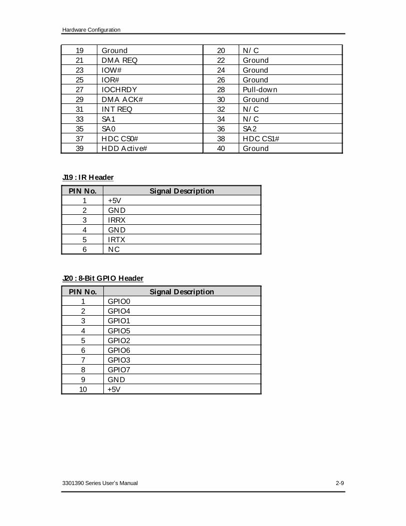
19 Ground 20 N/C21 DMA REQ 22 Ground23 IOW# 24 Ground25 IOR# 26 Ground27 IOCHRDY 28 Pull-down29 DMA ACK# 30 Ground31 INT REQ 32 N/C33 SA1 34 N/C35 SA0 36 SA237 HDC CS0# 38 HDC CS1#39 HDD Active# 40 Ground
J19 : IR Header
PIN No. Signal Description1 +5V2 GND3 IRRX4 GND5 IRTX6 NC
J20 : 8-Bit GPIO Header
PIN No. Signal Description1 GPIO02 GPIO43 GPIO14 GPIO55 GPIO26 GPIO67 GPIO38 GPIO79 GND
10 +5V
3301390 Series User s Manual 2-9

Hardware Configuration
J23 : DVI (TMDS) Panel Connector (Only for 3301390 )
PIN No. Signal Description PIN No. Signal Description1 TMDS_DATA0- 2 TMDS_DATA0+3 GND 4 GND5 TMDS_DATA1- 6 TMDS_DATA1+7 GND 8 GND9 TMDS_DATA2- 10 TMDS_DATA2+11 GND 12 GND13 TMDS_CLK- 14 TMDS_CLK+15 +5V 16 +5V17 DVI_DDCCLK 18 DVI_DDCDAT19 DVI_HPD 20 NC
J21/J22/J41/J42 : Serial ATA 1 /2/3/4
PIN No. Signal Description1,4,7 GND
2 TXP3 TXN5 RXN6 RXP
J24/J25 : Bracket Side USB Connector
PIN No. Signal Description1 Vcc (Stand By)2 D-3 D+4 GND
J26 : 4P Power Connector (Auxiliary Power)
PIN No. Signal Description1 +12V2 GND3 GND4 +5V
3301390 Series User s Manual 2-10
Hardware Configuration
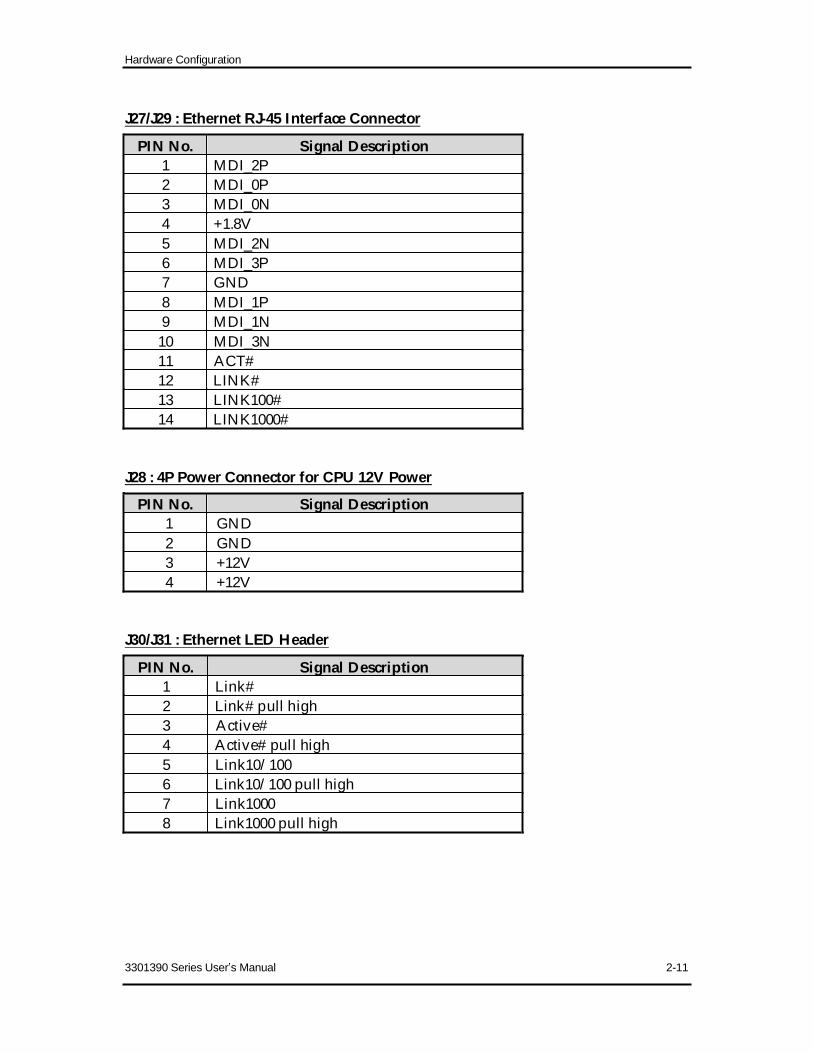
J27/J29 : Ethernet RJ-45 Interface Connector
PIN No. Signal Description1 MDI_2P2 MDI_0P3 MDI_0N4 +1.8V5 MDI_2N6 MDI_3P7 GND8 MDI_1P9 MDI_1N
10 MDI_3N11 ACT#12 LINK#13 LINK100#14 LINK1000#
J28 : 4P Power Connector for CPU 12V Power
PIN No. Signal Description1 GND2 GND3 +12V4 +12V
J30/J31 : Ethernet LED Header
PIN No. Signal Description1 Link#2 Link# pull high3 Active#4 Active# pull high5 Link10/1006 Link10/100 pull high7 Link10008 Link1000 pull high
3301390 Series User s Manual 2-11
Hardware Configuration
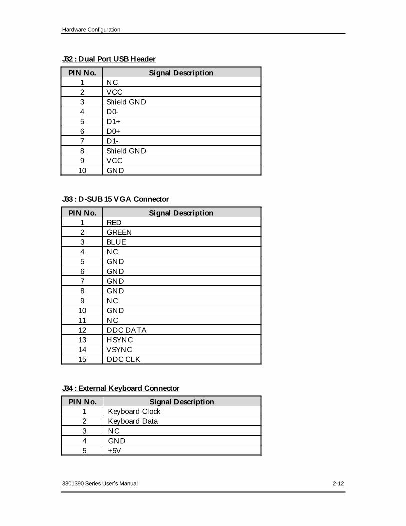
J32 : Dual Port USB Header
PIN No. Signal Description1 NC2 VCC3 Shield GND4 D0-5 D1+6 D0+7 D1-8 Shield GND9 VCC10 GND
J33 : D-SUB 15 VGA Connector
PIN No. Signal Description1 RED2 GREEN3 BLUE4 NC5 GND6 GND7 GND8 GND9 NC
10 GND11 NC12 DDC DATA13 HSYNC14 VSYNC15 DDC CLK
J34 : External Keyboard Connector
PIN No. Signal Description1 Keyboard Clock2 Keyboard Data3 NC4 GND5 +5V
3301390 Series User s Manual 2-12

Hardware Configuration
J36 : PS/2 Keyboard/Mouse Connector
PIN No. Signal Description1 Keyboard Data2 Mouse Data3 GND4 +5V5 Keyboard Clock6 Mouse Clock7 N/C8 N/C
J40 : CompactFlash Socket on IDE0 Master
Signal Description PIN No. Signal Description1 Ground 2 Data 33 Data 4 4 Data 55 Data 6 6 Data 77 SDCS#0 8 Ground9 Ground 10 Ground11 Ground 12 Ground13 +5V 14 Ground15 Ground 16 Ground17 Ground 18 SA219 SA1 20 SA021 Data 0 22 Data 123 Data 2 24 NC25 NC 26 NC27 Data 11 28 Data 1229 Data 13 30 Data 1431 Data 15 32 SDCS#333 Ground 34 IOR#35 IOW# 36 WE#37 INT 38 +5V39 Ground 40 NC41 RESET# 42 IORDY43 NC 44 REQ45 IDEACT# 46 PDIAG#47 Data 8 48 Data 949 Data 10 50 Ground
3301390 Series User s Manual 2-13

System Installation
Chapter 3System Installation
This chapter provides you with instructions to set up your system. The additionalinformation is enclosed to help you set up onboard PCI device and handle WDToperation in software programming.
3.1 Pentium M Processor
Installing mPGA 479M CPU1) Disengaging the Socket Actuator, use a screwdriver to disengage (open) the
socket actuator.
2) Align the processor pins with pin holes on the socket. Make sure that the notchedcorner or dot mark (pin 1) of the CPU corresponds to the socket’s bevel end. Thenpress the CPU gently until it fits into place. If this operation is not easy orsmooth, don’t do it forcibly. You need to check and rebuild the CPU pinuniformly.
3301390 Series User s Manual 3-1

System Installation
3) While gently holding the processor down with your finger, secure the processorin the socket by closing the socket actuator with a screwdriver.
4) Follow the installation guide of cooling fan or heat sink to mount it on CPUsurface and lock it on the socket 479M.
Note:You should know Pentium M / Celeron M processor need extra 12V power source.DON’T FORGET TO CONNECT 4-pin 12V connector to J28!
J28 : 4P Connector for CPU 12V Power
PIN No. Signal Description1 GND2 GND3 +12V4 +12V
Removing CPU
1) Unlock the cooling fan first.2) Lift the lever of CPU socket outwards and upwards to the other end.3) Carefully lifts up the existing CPU to remove it from the socket.4) Follow the steps of installing a CPU to change to another one or place handling
bar to close the opened socket.
Configuring System Bus
3301390 Series will automatically detect the CPU used. CPU speed of IntelPentium M can be detected automatically.
JP2 : CPU Type
JP2 Process Selection1-2 BaniasÌ2-3 Dothan
JP4 : CPU FSB Frequency Select
JP4 Process Selection1-2 100 MHÌ2-3 133 MH
3301390 Series User s Manual 3-2

System Installation
3.2 Main Memory
3301390 Series provides two 2 x 200-pin SODIMM sockets (dual channel) support1.8V DDR2 400/533 non-ECC DIMMs as on-board main memory. The maximummemory size can be up to 2GB. Auto detecting memory clock according to BIOSCMOS settings.
For system compatibility and stability, don’t use memory module without brand.You can also use only one double-sided DIMM in either one DIMM slot or twosingle-sided DIMM in both sockets.
Watch out the contact and lock integrity of memory module with socket, it willimpact on the system reliability. Follow normal procedures to install your DRAMmodule into memory socket. Before locking, make sure that all modules have beenfully inserted into the card slots.
Note:To maintain system stability, don’t change any of DRAM parameters in BIOS setupto upgrade your system performance without acquiring technical information.
Memory frequency / CPU FSB synchronizationMemory frequency supported by 3301390 Series depending on front side bus ofCPU, carefully choosing memory type according to the processor you want to installon the board. Following is table that helps you to select right memory typeaccording to different processor FSB.
CPU FSB Memory Frequency533MH 533/400MH400MH 400MH
3.3 Installing the Single Board Computer
To install your 3301390 Series into standard chassis or proprietary environment, youneed to perform the following:
Step 1: Check all jumpers setting on proper positionStep 2: Install and configure CPU and memory module on right positionStep 3: Place 3301390 Series into the dedicated position in your systemStep 4: Attach cables to existing peripheral devices and secure it
WARNINGPlease ensure that your SBC is properly inserted and fixed by mechanism.Otherwise, the system might be unstable or do not work due to bad contact ofPICMG 1.0 PCI plus ISA-bus slot.3301390 Series User s Manual 3-3

System Installation
Note:Please refer to section 3-3-1 to 3-3-4 to install INF/VGA/LAN/Audio drivers.
3301390 Series User s Manual 3-4

System Installation
3.3.1 Chipset Component Driver
The chipset on 3301390 Series is a new chipset that a few old operating systemsmight not be able to recognize. To overcome this compatibility issue, for WindowsOperating Systems such as Windows 2000/XP, please install its INF before any ofother Drivers are installed. You can find very easily this chipset component driver in3301390 / 3301390 CD-title. OS needs to modify according to OS that supported byIntel® 915GM & ICH6.
3.3.2 Intel Integrated Graphics GMCH Chip
Please find Intel 915 Graphic driver in the 3301390 CD-title. Drivers supportWindows 2000 / XP.
Please find ATI Mobility Graphic driver in the 3301390 CD-title. Drivers supportWindows 2000 / XP.
3301390 Series User s Manual 3-5

System Installation
3.3.3 On-board Gigabit Ethernet Controller
Drivers Support
Please find Marvell 88E8053 (via PCI-E) driver in /Ethernet directory of 3301390CD-title. The drivers support Windows 2000 / XP.
LED Indicator (for LAN status)3301390 Series provides three LED indicators to report Ethernet interfaces status.Please refer to the table below as a quick reference guide.
Operation of Ethernet Port
Green LAN Linked & Linked ActiveActive LED (Blinking)
LAN speed LEDAll Off N/A 10 MbpsGreen Speed LED 100 Mbps N/AAmber Speed LED 1000 Mbps N/A
3.3.4 On-board AC-97 Audio Device
Please find Realtek AC’97 Audio driver of 3301390 / 3301390 CD-title. Thedrivers support Windows 98SE / ME / 2000 / XP, and AC97 Utility.
3301390 Series User s Manual 3-6

System Installation
3.4 Clear CMOS Operation
The following table indicates how to enable/disable CMOS Clear Function hardwarecircuit by putting jumpers at proper position.
JP7 : RTC CMOS Clear Jumper Setting
JP7 Process Selection1-2 Normal OperationÌ2-3 Clear CMOS Contents
To correctly operate CMOS Clear function, users must turn off the system, move JP7jumper to short pin 2 and 3. To clear CMOS contents, please turn the power back onand turn it off again for AT system, or press the toggle switch a few times for ATXsystem. Move the JP7 back to 1-2 position (Normal Operation) and start the system.Users then load BIOS default setting.
3.5 WDT Function
The working algorithm of the WDT function can be simply described as a countingprocess. The Time-Out Interval can be set through software programming. Theavailability of the time-out interval settings by software or hardware varies fromboards to boards.
3301390 allows users control WDT through dynamic softwareprogramming. The WDT starts counting when it is activated. It sends out a signal tosystem reset, when time-out interval ends. To prevent the time-out interval fromrunning out, a re-trigger signal will need to be sent before the counting reaches itsend. This action will restart the counting process. A well-written WDT programshould keep the counting process running under normal condition. WDT shouldnever generate a system reset unless the system runs into troubles.
The related Control Registers of WDT are all included in the following sampleprogram that is written in C language. User can fill a non-ero value into the Time-out Value Register to enable/refresh WDT. System will be reset after the Time-outValue to be counted down to ero. Or user can directly fill a ero value into Time-outValue Register to disable WDT immediately. To ensure a successful accessing to thecontent of desired Control Register, the sequence of following program codes shouldbe step-by-step run again when each register is accessed.
Additionally, there are maximum 2 seconds of counting tolerance that should beconsidered into user’ application program. For more information about WDT, pleaserefer to Winbond W83627THF data sheet.
3301390 Series User s Manual 3-7

System Installation
There are two PNP I/O port addresses that can be used to configure WDT,1) 0x2E:EFIR (Extended Function Index Register, for identifying CR index number)2) 0x2F:EFDR (Extended Function Data Register, for accessing desired CR)
Below are some example codes, which demonstrate the use of WDT.// Enter Extended Function Modeoutp(0x002E, 0x87);outp(0x002E, 0x87);// Assign Pin 89 to be a WDTOoutp(0x002E, 0x2B);outp(0x002F, inp(0x002F) & 0xEF);// Select Logic Device 8outp(0x002E, 0x07);outp(0x002F, 0x08);// Active Logic Device 8outp(0x002E, 0x30);outp(0x002F, 0x01);// Select Count Modeoutp(0x002E, 0xF5);outp(0x002F, (inp(0x002F) & 0xF7) | ( Count-mode Register & 0x08));// Specify Time-out Valueoutp(0x002E, 0xF6);outp(0x002F, Time-out Value Register );// Disable WDT reset by keyboard/mouse interruptsoutp(0x002E, 0xF7);outp(0x002F, 0x00);// Exit Extended Function Modeoutp(0x002E, 0xAA);
Definitions of Variables:
Value of Count-mode Register :1) 0x00 -- Count down in seconds (Bit3=0)2) 0x08 -- Count down in minutes (Bit3=1)Value of Time-out Value Register :1) 0x00 -- Time-out Disable2) 0x01~0xFF -- Value for counting down
3301390 Series User s Manual 3-8

System Installation
3.6 GPIO
The 3301390 Series provides 8 programmable input or output ports that can beindividually configured to perform a simple basic I/O function. Users can configureeach individual port to become an input or output port by programming register bitof I/O Selection. To invert port value, the setting of Inversion Register has to bemade. Port values can be set to read or write through Data Register.
Pin assignment
J20 : 8-Bit GPIO Header
PIN No. Signal Description1 General Purpose I/O Port 0 (GPIO0)2 General Purpose I/O Port 4 (GPIO4)3 General Purpose I/O Port 1 (GPIO1)4 General Purpose I/O Port 5 (GPIO5)5 General Purpose I/O Port 2 (GPIO2)6 General Purpose I/O Port 6 (GPIO6)7 General Purpose I/O Port 3 (GPIO2)8 General Purpose I/O Port 7 (GPIO7)9 Ground
10 +5V
All General Purpose I/O ports can only apply to standard TTL ± 5% signal level(0V/5V), and each source sink capacity up to 12mA.
3301390 GPIO Programming Guide
There are 8 GPIO pins on 3301390 Series. These GPIO pins are from SUPER I/O(W83627THF) GPIO pins, and can be programmed as Input or Output direction. J20pin header is for 8 GPIO pins and its pin assignment as following :
J20_Pin1=GPIO0:from SUPER I/O_GPIO10 with Ext. 4.7K PHJ20_Pin2=GPIO4:from SUPER I/O_GPIO14 with Ext. 4.7K PHJ20_Pin3=GPIO1:from SUPER I/O_GPIO11 with Ext. 4.7K PHJ20_Pin4=GPIO5:from SUPER I/O_GPIO15 with Ext. 4.7K PHJ20_Pin6=GPIO2:from SUPER I/O_GPIO12 with Ext. 4.7K PHJ20_Pin7=GPIO6:from SUPER I/O_GPIO16 with Ext. 4.7K PHJ20_Pin8=GPIO3:from SUPER I/O_GPIO13 with Ext. 4.7K PHJ20_Pin9=GPIO7:from SUPER I/O_GPIO17 with Ext. 4.7K PH
<<<<< Be careful Pin9=GND , Pin10=VCC >>>>>
3301390 Series User s Manual 3-9

System Installation
There are several Configuration Registers (CR) of W83627THF needed to beprogrammed to control the GPIO direction, and status(GPI)/value(GPO). CR02h ~CR2F are common (global) registers to all Logical Devices (LD) in W83627THF.CR07h contains the Logical Device Number that can be changed to access the LD asneeded. LD7 contains the GPIO10~17 registers.
Programming Guide:
Step1: CR29_Bit [7.6]. P [0,1]; to select multiplexed pins as GPIO10~17 pinsStep2: CR07h.P [07h]; Point to LD7Step3: LD7_CR30h_Bit0.P1; Enable LD7Step4: Select GPIO direction, Get Status or output value.
LD7_CRF0h; GPIO17 ~ 10 direction, 1 = input, 0 = output pinLD7_CRF2h.P[00h]; Let CRF1 (GPIO data port) non-invert to prevent from confusionLD7_CRF1h; GPIO17~10 data port, for input pin, get status from the related bit, foroutput pin, write value to the related bit.
For example,LD7_CRF0h_Bit4.P0; Let GPIO14 as output pinLD7_CRF2h_Bit4.P0; Let CRF1_Bit4 non-invertedLD7_CRF1h_Bit4.P0; Output “0” to GPIO14 pin (J20_Pin2)LD7_CRF0h_Bit0.P1; Let GPIO10 as input pinLD7_CRF2h_Bit0.P0; Let CRF1_Bit0 non-invertedRead LD7_CRF1h_Bit0; Read the status from GPIO10 pin (J20_Pin1)
How to access W83627THF CR?In 3301390 Series, the EFER = 002Eh, and EFDR = 002Fh. EFERand EFDR are 2 IO ports needed to access W83627THF CR. EFERis the Index Port, EFDR is the Data Port.CR index number needs to be written into EFER first,Then the data will be read/written from/to EFDR.To R/W W83627THF CR, it is needed to Enter/Enable Configuration Mode first.When completing the programming, it is suggested to Exit/Disable ConfigurationMode.
Enter Configuration Mode: Write 87h to IO port EFER twice.Exit Configuration Mode: Write AAh to IO port EFER.
3301390 Series User s Manual 3-10

System Installation
Example
Define GPIO4 as output pin, and output “0” to this pin.
mov dx,2eh ; Enter Configuration Modemov al,87hout dx,aljmp $+2out dx,al
mov dx,2ehmov al,29h ; Read CR29out dx,almov dx,2fhin al,dxand al,3Fhor al,40h ; CR29_Bit[7..6].P[0,1]mov ah,almov dx,2ehmov al,2Ahout dx,almov dx,2fhmov al,ahout dx,almov dx,2ehmov al,07h ; Point to LDN7out dx,almov dx,2fhmov al,07hout dx,al
mov dx,2eh ; Read CR30mov al,30hout dx,almov dx,2fhin al,dxor al,01hmov ah,almov dx,2eh ; CR30_Bit0.P1mov al,30hout dx,almov dx,2fhmov al,ahout dx,al
3301390 Series User s Manual 3-11

System Installation
mov dx,2ehmov al,0f0h ; Read LD7_CRF0out dx,almov dx,2fhin al,dxand al,0efhmov ah,al
mov dx,2ehmov al,0f0h ; LD7_CRF0_Bit4.P0out dx,almov dx,2fhmov al,ahout dx,al
mov dx,2ehmov al,0f2h ; Read LD7_CRF2out dx,almov dx,2fhin al,dxand al,0efhmov ah,al
mov dx,2ehmov al,0f2h ; LD7_CRF2_Bit4.P0out dx,almov dx,2fhmov al,ahout dx,al
mov dx,2ehmov al,0f1h ; Read LD7_CRF1out dx,almov dx,2fhin al,dxand al,0efhmov ah,al
mov dx,2ehmov al,0f1h ; LD7_CRF1_Bit4.P0out dx,almov dx,2fhmov al,ahout dx,al
3301390 Series User s Manual 3-12

System Installation
mov dx,2eh ; Exit Configuration Modemov al,0AAhout dx,al
3301390 Series User s Manual 3-13

BIOS Setup Information
Chapter 4BIOS Setup Information
3301390 Series is equipped with the AWARD BIOS stored in Flash ROM. TheseBIOS has a built-in Setup program that allows users to modify the basic systemconfiguration easily. This type of information is stored in CMOS RAM so that it isretained during power-off periods. When system is turned on, 3301390 Seriescommunicates with peripheral devices and checks its hardware resources against theconfiguration information stored in the CMOS memory. If any error is detected, orthe CMOS parameters need to be initially defined, the diagnostic program willprompt the user to enter the SETUP program. Some errors are significant enough toabort the start-up.
4.1 Entering Setup
Turn on or reboot the computer. When the message “Hit <DEL> if you want to runSETUP” appears, press <Del> key immediately to enter BIOS setup program.
If the message disappears before you respond, but you still wish to enter Setup,please restart the system to try “COLD START” again by turning it OFF and thenON, or touch the "RESET" button. You may also restart from “WARM START” bypressing <Ctrl>, <Alt>, and <Delete> keys simultaneously. If you do not pressthe keys at the right time and the system will not boot, an error message will bedisplayed and you will again be asked to,
Press <F1> to Run SETUP or ResumeIn HIFLEX BIOS setup, you can use the keyboard to choose among options ormodify the system parameters to match the options with your system. The tablebelow will show you all of keystroke functions in BIOS setup.
General Help: Move
Enter : Select+ / - /PU /PD : ValueESC : ExitF1 : General HelpF2 : Item HelpF5 : Previous ValuesF6 : Fail-Safe DefaultsF7 : Optimized DefaultsF9 : Menu in BIOSF10 : Save
3301390 Series User s Manual 4-1

BIOS Setup Information
4.2 Main Menu
Once you enter 3301390 Series AWARD BIOS CMOS Setup Utility, you shouldstart with the Main Menu. The Main Menu allows you to select from eleven setupfunctions and two exit choices. Use arrow keys to switch among items and press<Enter> key to accept or bring up the sub-menu.
Phoenix- Award BIOS CMOS Setup Utility
f Standard CMOS Features f Frequency/Voltage Controlf Advanced BIOS Features Load Fail-Safe Defaultsf Advanced Chipset Features Load Optimized Defaultsf Integrated Peripherals Set Supervisor Passwordf Power Management Setup Set User Passwordf PnP/PCI Configurations Save & Exit Setupf PC Health Status Exit Without Saving
ESC : Quit F9 : Menu in BIOS : Select ItemF10 : Save & Exit Setup
Time, Date, Hard Disk Type …
Note:It is strongly recommended to reload Optimal Setting if CMOS is lost or BIOS isupdated.
3301390 Series User s Manual 4-2
BIOS Setup Information
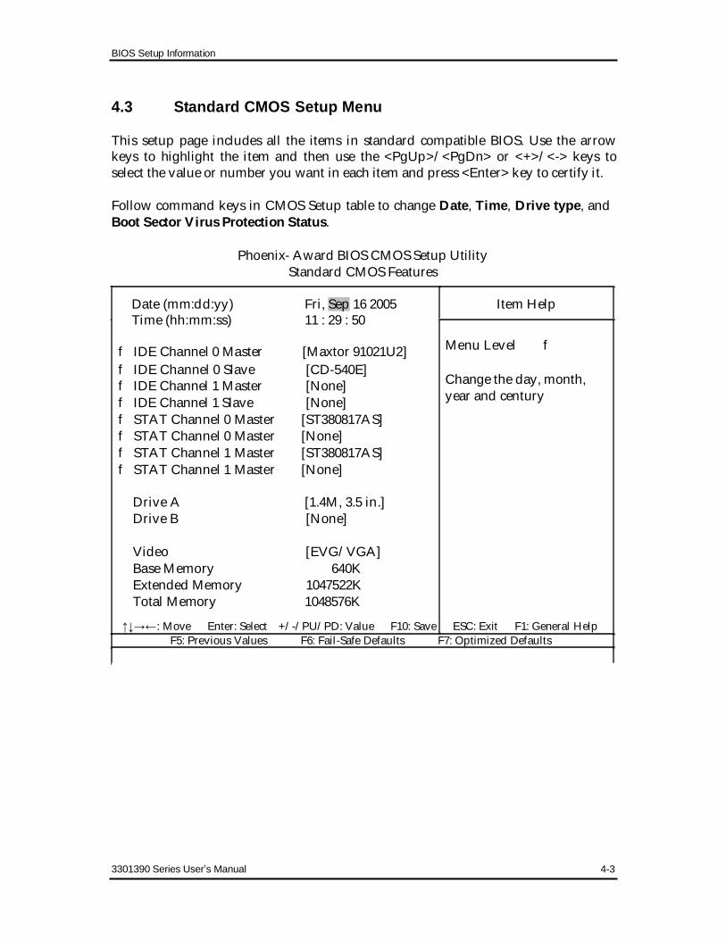
4.3 Standard CMOS Setup Menu
This setup page includes all the items in standard compatible BIOS. Use the arrowkeys to highlight the item and then use the <PgUp>/<PgDn> or <+>/<-> keys toselect the value or number you want in each item and press <Enter> key to certify it.
Follow command keys in CMOS Setup table to change Date, Time, Drive type, andBoot Sector Virus Protection Status.
Phoenix- Award BIOS CMOS Setup UtilityStandard CMOS Features
Date (mm:dd:yy) Fri, Sep 16 2005 Item HelpTime (hh:mm:ss) 11 : 29 : 50
f IDE Channel 0 Master [Maxtor 91021U2] Menu Level f
f IDE Channel 0 Slave [CD-540E]f IDE Channel 1 Master [None] Change the day, month,
f IDE Channel 1 Slave [None] year and century
f STAT Channel 0 Master [ST380817AS]f STAT Channel 0 Master [None]f STAT Channel 1 Master [ST380817AS]f STAT Channel 1 Master [None]
Drive A [1.4M, 3.5 in.]Drive B [None]
Video [EVG/VGA]Base Memory 640KExtended Memory 1047522KTotal Memory 1048576K
: Move Enter: Select +/-/PU/PD: Value F10: Save ESC: Exit F1: General HelpF5: Previous Values F6: Fail-Safe Defaults F7: Optimized Defaults
3301390 Series User s Manual 4-3

BIOS Setup Information
Menu SelectionsItem Options Description
Date mm:dd:yy Change the day, month, year andcentury
Time hh:mm:ss Change the internal clockIDE Channel 0 Options are in its sub Press <Enter> to enter the sub menu ofMaster menu detailed optionsIDE Channel 0 Options are in its sub Press <Enter> to enter the next pageSlave menu for detail hard drive settingsIDE Channel 1 Options are in its sub Press <Enter> to enter the next pageMaster menu for detail hard drive settingsIDE Channel 1 Options are in its sub Press <Enter> to enter the next pageSlave menu for detail hard drive settingsSTAT0 Master Options are in its sub Press <Enter> to enter the next page
menu for detail hard drive settingsSTAT1 Master Options are in its sub Press <Enter> to enter the next page
menu for detail hard drive settingsDrive A None Press <Enter> to enter the next pageDrive B 360K, 5.25 in for detail hard drive settings
1.2M, 5.25 in720K, 3.5 in1.44M, 3.5 in2.88M, 3.5 in
Video EGA/VGA Select the default video deviceCGA 40CGA 80MONO
Base Memory 640K Displays the amount of conventional
memory detected during boot upExtended Displays the amount of extendedMemory N/A memory detected during boot up
Total Memory N/A Displays the total memory available in
the system
3301390 Series User s Manual 4-4

BIOS Setup Information
4.4 IDE Adaptors Setup Menu
The IDE adapters control the IDE devices, such as hard disk drive or CDROM drive.It uses a separate sub menu to configure each hard disk drive.
Phoenix- Award BIOS CMOS Setup UtilityIDE Channel 0 Master
IDE HDD Auto-Detection [Press Enter] Item Help
IDE Channel 0 Master [Auto]Access Mode [Auto] Menu Level f
Capacity 10246 MB To auto-detect the HDD’s
size, head … on this
Cylinder 19852 channel
Head 16Precomp 0Landing one 19851Sector 63
: Move Enter: Select +/-/PU/PD: Value F10: Save ESC: Exit F1: General HelpF5: Previous Values F6: Fail-Safe Defaults F7: Optimized Defaults
Menu SelectionsItem Options Description
IDE HDD Auto- Press Enter Press Enter to auto-detect the HDD ondetection this channel. If detection is
successful, it fills the remaining fieldson this menu.
IDE Channel 0 None Selecting ‘manual’ lets you set theMaster Auto remaining fields on this screen. Selects
Manual the type of fixed disk. "User Type" willlet you select the number of cylinders,heads, etc.Note: PRECOMP=65535 means NONE!
Access Mode CHS Choose the access mode for this hardLBA diskLargeAuto
The following options are selectable only if the ‘IDE Channel 0 Master ‘item is setto ‘Manual’
3301390 Series User s Manual 4-5

BIOS Setup Information
Capacity Auto Display your disk Disk drive capacity (Approximated).drive size Note that this size is usually slightly
greater than the size of a formatteddisk given by a disk-checkingprogram.
Cylinder Min = 0 Set the number of cylinders for thisMax = 65535 hard disk.
Head Min = 0 Set the number of read/write headsMax = 255
Precomp Min = 0 **** Warning: Setting a value of 65535Max = 65535 means no hard disk
Landing one Min = 0 ****Max = 65535
Sector Min = 0 Number of sectors per trackMax = 255
Phoenix- Award BIOS CMOS Setup UtilitySATA 0 Master
IDE HDD Auto-Detection [Press Enter] Item Help
Extended IDE Drive [Auto]Access Mode [Auto] Menu Level f
Capacity 80GB To auto-detect the HDD’s
size, head … on this
Cylinder 38309 channel
Head 16Precomp 0Landing one 38308Sector 255
: Move Enter: Select +/-/PU/PD: Value F10: Save ESC: Exit F1: General HelpF5: Previous Values F6: Fail-Safe Defaults F7: Optimized Defaults
3301390 Series User s Manual 4-6

BIOS Setup Information
Menu SelectionsItem Options Description
IDE HDD Auto- Press Enter Press Enter to auto-detect the HDD ondetection this channel. If detection is
successful, it fills the remaining fieldson this menu.
Extended IDE NoneDrive AutoAccess Mode Large Choose the access mode for this hard
Auto diskThe following options are selectable only if the ‘STAT Channel 0 Master ‘item is setto ‘Manual’Capacity Auto Display your disk Disk drive capacity (Approximated).
drive size Note that this size is usually slightlygreater than the size of a formatteddisk given by a disk-checkingprogram.
Cylinder Min = 0 Set the number of cylinders for thisMax = 65535 hard disk.
Head Min = 0 Set the number of read/write headsMax = 255
Precomp Min = 0 **** Warning: Setting a value of 65535Max = 65535 means no hard disk
Landing one Min = 0 ****Max = 65535
Sector Min = 0 Number of sectors per trackMax = 255
3301390 Series User s Manual 4-7
BIOS Setup Information
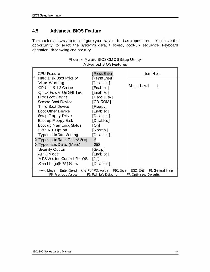
4.5 Advanced BIOS Feature
This section allows you to configure your system for basic operation. You have theopportunity to select the system’s default speed, boot-up sequence, keyboardoperation, shadowing and security.
Phoenix- Award BIOS CMOS Setup UtilityAdvanced BIOS Features
f CPU Feature [Press Enter] Item Helpf Hard Disk Boot Priority [Press Enter]
Virus Warning [Disabled]CPU L1 & L2 Cache [Enabled] Menu Level f
Quick Power On Self Test [Enabled]First Boot Device [Hard Disk]Second Boot Device [CD-ROM]Third Boot Device [Floppy]Boot Other Device [Enabled]Swap Floppy Drive [Disabled]Boot up Floppy Seek [Disabled]Boot up NumLock Status [On]Gate A20 Option [Normal]Typematic Rate Setting [Disabled]
X Typematic Rate (Chars/Sec) 6X Typematic Delay (Msec) 250
Security Option [Setup] APIC Mode [Enabled]
MPS Version Control For OS [1.4]Small Logo(EPA) Show [Disabled]
: Move Enter: Select +/-/PU/PD: Value F10: Save ESC: Exit F1: General HelpF5: Previous Values F6: Fail-Safe Defaults F7: Optimized Defaults
3301390 Series User s Manual 4-8

BIOS Setup Information
Phoenix- Award BIOS CMOS Setup UtilityCPU Feature
Delay Prior to Thermal [16 Min] Item HelpThermal Management [Thermal Monitor 1]
X TM2 Bus Ratio 16XX TM2 Bus VID 0.860V Menu Level f
: Move Enter: Select +/-/PU/PD: Value F10: Save ESC: Exit F1: General HelpF5: Previous Values F6: Fail-Safe Defaults F7: Optimized Defaults
Delay Prior to Thermal
The choice: 4 Min, 8 Min, 16 Min, and 32 Min.
Thermal Management
Thermal Monitor 1 (On die throttling); Thermal Monitor 2 (Ratio & VID transition)
The choice: Thermal Monitor 1, Thermal Monitor 2.
Phoenix- Award BIOS CMOS Setup UtilityHard Disk Boot Priority
1. ch0 M. : Maxtor 91021U2 Item Help2. ch2 M. : ST380817AS3. ch3 M. : ST380817AS4. Bootable add-in Cards Menu Level f
Use < > or < > to select adevice, then press <+> tomove it up, or <-> to moveit down the list. Press<ESC> to exit this menu.
: Move Enter: Select +/-/PU/PD: Value F10: Save ESC: Exit F1: General HelpF5: Previous Values F6: Fail-Safe Defaults F7: Optimized Defaults
Hard Disk Boot PrioritySelect Hard Disk Boot Device Priority. Use < > or < > to select a device, thenpress <+> to move it up, or <-> to move it down the list. Press <ESC> to exit thismenu.
Bootable Add-in Cards Select SCSI Device BootCh x M (S). Select IDE Channel 0,1 Master or Salve BootCh x M. Select IDE Channel 2 or 3 Master Boot
3301390 Series User s Manual 4-9

BIOS Setup Information
Virus WarningAllow you to choose the VIRUS warning feature for IDE Hard Disk boot sectorprotection. If this function is enabled and someone attempt to write data into thisarea, BIOS will show a warning message on screen and alarm beep.
Activates automatically when the system boots up causing aEnabled warning message to appear when anything attempts to access the
boot sector or hard disk partition table.
Disabled No warning message will appear when anything attempts to access
the boot sector or hard disk partition table.
CPU L1 Cache/L2 Cache
These two categories speed up memory access. However, it depends onCPU/chipset design.
Enabled Enable CacheDisabled Disable Cache
Quick Power On Self TestAllows the system to skip certain tests while booting. This will decrease the timeneeded to boot the system.
Enabled Enable quick POSTDisabled Normal POST
First/Second/Third Boot Device
Select your boot device priority.
The choice: Floppy, LS120, Hard Disk, CDROM, IP 100, USB-FDD, USB-IP, USB-CDROM, and Disabled.
Boot Other DeviceSelect your boot device priority.The choice: Enabled, Disabled.Swap Floppy Drive
If the system has two floppy drives, choose enable to assign physical driver B tological drive A and Vice-Versa.
The choice: Enabled, Disabled.
3301390 Series User s Manual 4-10

BIOS Setup Information
Boot Up Floppy Seek
Enabled tests floppy drives to determine whether they have 40 or 80 tracks.
The choice: Enabled, Disabled.
Boot Up NumLock Status
Select power on state for NumLock.
The choice: Off, On.
Gate A20 OptionFast-lets chipsets control Gate A20 and Normal – a pin in the keyboard controllercontrols Gate A20. Default is Fast.
The choice: Normal, Fast.
Typematic Rate SettingKeystrokes repeat at a rate determined by the keyboard controller – When enabled,the typematic rate and typematic delay can be selected.
The choice: Enabled, Disabled.
Typematic Rate (Chars/sec)
The rate at which character repeats when you hold down a key.
The choice: 6, 8, 10, 12, 15, 20, 24, and 30.
Typematic delay (Msec)
The delay before keystrokes begin to repeat.
The choice: 250, 500, 750, and 1000.
Security OptionSelect whether the password is required every time the system boots or only whenyou enter setup.
System The system will not boot and access to Setup will be denied if the
correct password is not entered at the prompt.
Setup The system will boot, but access to Setup will be denied if the
correct password is not entered at the prompt.
3301390 Series User s Manual 4-11

BIOS Setup Information
APIC Mode
The choice: Enabled, Disabled.
MPS Version Control For OS
The choice: 1.1, 1.4.
Small Logo (EPA) Show
The choice: Enabled, Disabled.
3301390 Series User s Manual 4-12

BIOS Setup Information
4.6 Advanced Chipset Feature
This section allows you to configure the system based on the specific features of theIntel 915GM chipset. This chipset manages bus speeds and access to systemmemory resources, such as DRAM (DDR II SO-DRAM) and the external cache. Italso coordinates communications between the conventional ISA bus and the PCIbus. It must be stated that these items should never need to be altered. Thedefault settings have been chosen because they provide the best operating conditionsfor your system. The only time you might consider making any changes would beif you discovered that data was being lost while using your system.
Phoenix- Award BIOS CMOS Setup UtilityAdvanced Chipset Features
DRAM Timing Selectable [By SPD] Item HelpX CAS Latency Time 4X DRAM RAS# to CAS# Delay 3X DRAM RAS# Precharge 3 Menu Level f
X Precharge delay (tRAS) 9X System Memory Frequency 400MH
SLP_S4# Assertion Width [1 to 2 Sec.]System BIOS Cacheable [Enabled]Video BIOS Cacheable [Enabled]Memory Hole At 15M-16M [Disabled]TV-Out Mode [NTSC]
** On-Chip VGA Setting **On-Chip Frame Buffer Size [ 8MB]DVMT Mode [DVMT]DVMT /FIXED Memory Size [128MB]Boot Display [CRT]Panel Scaling [Auto]Panel Type [640X480 18bit 1ch]TV Standard [Off]Video Connector [Automatic]TV Format [Auto]FWH Write Protection [Disabled]BootBlock Protection [Disabled]
: Move Enter: Select +/-/PU/PD: Value F10: Save ESC: Exit F1: General HelpF5: Previous Values F6: Fail-Safe Defaults F7: Optimized Defaults
3301390 Series User s Manual 4-13

BIOS Setup Information
This chipset settings deal with CPU access to dynamic random access memory(DRAM). The default timings have been carefully chosen and should only be alteredif data is being lost. Such a scenario might well occur if your system had mixedspeed DRAM chips installed so that greater delays may be required to preserve theintegrity of the data held in the slower memory chips.
DRAM Timing Selectable
This option provides DIMM plug-and-play support by serial presence detect (SPD)mechanism via the system management bus (SMBUS) interface.
The choice: Manual, By SPD.
CAS Latency TimeThis option controls the number of SCLKs between the time a read command issampled by the DRAMs and the time the GMCH samples correspondent data fromthe DRAMs.
The choice: 3, 4, 5 and Auto.
DRAM RAS# to CAS# DelayThis option controls the number of SCLKs (SDRAM Clock) from a row activatecommand to a read or write command. If your system installs good quality ofSDRAM, you can set this option to “3 SCLKs” to obtain better memory performance.Normally, the option will be set to Auto.
The choice: 2, 3, 4, 5 and Auto.
DRAM RAS# PrechargeThis option controls the number of SCLKs for RAS# precharge. If your systeminstalls good quality of SDRAM, you can set this option to “3 SCLKs” to obtainbetter memory performance. It is set to auto normally.
The choice: 2, 3, 4, 5 and Auto.
Precharge delay (tRAS)
The choice: 4, 5, 6, 7, 8, 9, 10, 11, 12, 13, 14, and 15, Auto.
System Memory Frequency
Users are recommended to use Auto for memory frequency selection.
The choice: 333MH, 400MH, 533MH and Auto.
3301390 Series User s Manual 4-14

BIOS Setup Information
SLP_S4# Assertion Width
The choice: 4 to 5 Sec., 3to 4 Sec, 2 to 3 Sec., 1 to 2 Sec.
System BIOS CacheableSelecting Enabled allows caching of the system BIOS ROM at F0000h-FFFFFh,resulting in better system performance. However, if any program writes to thismemory area, a system error may result.
The choice: Enabled, Disabled.
Video BIOS CacheableSelect “Enabled” to enable caching VGA BIOS into L2 cache to get higher displayperformance. “Disabled” to ignore this BIOS caching function.
The choice: Enabled, Disabled.
Memory Hole At 15-16MIn order to improve performance, certain space in memory is reserved for ISA cards.This memory must be mapped into the memory space below 16MB.
The choice: Enabled, Disabled.
TV-Out Mode (Only for 3301390)
The choice: NTSC, PAL, PAL-M, PAL-N.
On-Chip Frame Buffer Size (Only for 3301390)
The choice: 1MB, 8MB.
DVMT Mode (Only for 3301390)
The choice: DVMT, FIXED and BOTH.
DVMT /FIXED Memory Size (Only for 3301390)
The choice: 64MB, 128MB.
Boot Display (Only for 3301390)
The choice: CRT, LVDS, CRT+LVDS, TV, and CRT+TV.
Panel Scaling (Only for 3301390)
The choice: Auto, On, Off.
3301390 Series User s Manual 4-15

BIOS Setup Information
Panel Type (Only for 3301390)
The choice: 640X480 18bit 1ch, 800X600 18bit 1ch, 1024X768 18bit 1ch, 1024X768 24bit1ch, 1280X1024 24bit 1ch, 1280X1024 24bit 2ch, 1400X1050 18bit 2ch, and1600X1200 24bit 2ch.
TV Standard (Only for 3301390)
The choice: Off, NTSC, PAL, and SECAM.
Video Connector (Only for 3301390)
The choice: Automatic, Composite, and Component, Both.
TV Format (Only for 3301390)The choice: Auto, NTSC_M, NTSC_M_J, NTSC_433, NTSC_N, PAL_B, PAL_G,
PAL_D, PAL_H, PAL_I, PAL_N, PAL_60, SECAM_L, SECAM_L1,SECAM_B, SECAM_D, SECAM_G, SECAM_H, SECAM_K, SECAM_K1.
FWH Write Protection
The choice: Enabled, Disabled.
BootBlock Protection
The choice: Enabled, Disabled.
4.7 Integrated Peripherals
Phoenix- Award BIOS CMOS Setup UtilityIntegrated Peripherals
f OnChip IDE Device [Press Enter] Item Helpf Onboard Device [Press Enter]f Super IO Device [Press Enter]
Menu Level f
: Move Enter: Select +/-/PU/PD: Value F10: Save ESC: Exit F1: General HelpF5: Previous Values F6: Fail-Safe Defaults F7: Optimized Defaults
3301390 Series User s Manual 4-16

BIOS Setup Information
Phoenix- Award BIOS CMOS Setup UtilityOnChip IDE Device
IDE HDD Block Mode [Enabled] Item HelpIDE DMA transfer access [Enabled]On-Chip Primary PCI IDE [Enabled]IDE Primary Master PIO [Auto] Menu Level f
IDE Primary Slave PIO [Auto]IDE Primary Master UDMA [Auto] If your IDE hard drive
IDE Primary Slave UDMA [Auto] supports block mode select
On-Chip Secondary PCI IDE [Enabled] Enabled for automatic
IDE Secondary Master PIO [Auto] detection of the optimal
IDE Secondary Slave PIO [Auto] number of block
IDE Secondary Master UDMA [Auto] read/writes per sector the
IDE Secondary Slave UDMA [Auto] drive can support
*** On-Chip Serial ATA Setting ***SATA Mode [IDE]On-Chip Serial ATA [Enhanced Mode]
X PATA IDE Mode SecondarySATA Port P0, P2 is Secondary
: Move Enter: Select +/-/PU/PD: Value F10: Save ESC: Exit F1: General HelpF5: Previous Values F6: Fail-Safe Defaults F7: Optimized Defaults
IDE HDD Block ModeIf you’re IDE hard drive supports block mode select Enabled for automaticdetection of the optimal number of block read/writes per sector the drive cansupport.
The choice: Enabled, Disabled.
IDE DMA transfer access
The choice: Enabled, Disabled.
OnChip Primary/Secondary PCI IDEThe chipset contains a PCI IDE interface with support for two IDE channels. SelectEnabled to activate the primary IDE interface. Select Disabled to deactivate thisinterface.
The choice: Enabled, Disabled.
3301390 Series User s Manual 4-17

BIOS Setup Information
IDE Primary/Secondary Master/Slave PIOThe four IDE PIO (Programmed Input/Output) fields let you set a PIO mode (0-4)for each of the four IDE devices that the onboard IDE interface supports. Modes 0through 4 provide successively increased performance. In Auto mode, the systemautomatically determines the best mode for each device.
The choice: Auto, Mode 0, Mode 1, Mode 2, Mode 3, and Mode 4.
IDE Primary/Secondary Master/Slave UDMAUltra DMA/33/66/100 implementation is possible only if your IDE hard drivesupports it and the operating environment includes a DMA driver (Windows 95OSR2 or a third-party IDE bus master driver). If your hard drive and your systemsoftware both support Ultra DMA/33/66/100, select Auto to enable BIOS support.
The choice: Auto, Disabled.
SATA Mode
The choice: IDE, AHCI.
On-Chip Serial ATA
Disabled Disabled SATA ControllerEnhanced Mode Enable both SATA and PATA. Max. Of 6 IDE drives are
SupportedSATA Only SATA is operating in legacy mode
Phoenix- Award BIOS CMOS Setup UtilityOnboard Device
USB Controller [Enabled] Item HelpUSB 2.0 Controller [Enabled]USB Keyboard Support [Enabled]USB Mouse Support [Disabled] Menu Level f
Aalia AC97 Audio Select [Auto]
: Move Enter: Select +/-/PU/PD: Value F10: Save ESC: Exit F1: General HelpF5: Previous Values F6: Fail-Safe Defaults F7: Optimized Defaults
USB Controller
This item allows you to enable/disable USB (Universal Serial Bus) function.
The choice: Enabled, Disabled.
3301390 Series User s Manual 4-18

BIOS Setup Information
USB 2.0 ControllerThis entry is for disable/enable EHCI controller only. This BIOS itself may/maynot have high speed USB support built in, the support will be automatically turn onwhen high speed device were attached.
The choice: Enabled, Disabled.
USB Keyboard SupportThis item allows you to enable USB keyboard function under POST, BIOS setupmenu, DOS, or Windows-NT with no USB driver loaded.
The choice: Enabled, Disabled.
USB Mouse SupportThis item allows you to enabled USB Mouse function under POST, BIOS Setupmenu, DOS, or Window-NT with no USB driver loaded.
The choice: Enabled, Disabled.
Aalia AC97 Audio SelectUsers can disable on board AC97 Audio function.
The choice: Auto, Aalia, AC97 Audio, and Disabled.
Phoenix- Award BIOS CMOS Setup UtilitySuper IO Device
Onboard FDC Controller [Enabled] Item HelpOnboard Serial Port 1 [3F8/IRQ4]Onboard Serial Port 2 [2F8/IRQ3]UART Mode Select [Normal] Menu Level f
X RxD, TxD Active Hi, LoX IR Transmission Delay EnabledX UR2 Duplex Mode HalfX Use IR Pins IR-Rx2Tx2
Onboard Parallel Port [378/IRQ7]Parallel Port Mode [SPP]
X EPP Mode Select EPP1.7X ECP Mode Use DMA 3
PWRON After PWR-Fail [Off]
: Move Enter: Select +/-/PU/PD: Value F10: Save ESC: Exit F1: General HelpF5: Previous Values F6: Fail-Safe Defaults F7: Optimized Defaults
3301390 Series User s Manual 4-19

BIOS Setup Information
Onboard FDC Controller
This item allows you to enable/disable onboard Floppy disk controller.
The choice: Enabled, Disabled.
Onboard Serial Port 1/Port 2
Select an address and corresponding interrupt for the first and second serial ports.
The choice: 3F8/IRQ4, 2F8/IRQ3, 3E8/IRQ4, 2E8/IRQ3, Disabled, Auto.
UART Mode Select
This item allows users to select Infrared transmission mode.
Normal Disable Infrared functionIrDA Select IrDA mode transmissionASKIR Select ASKIR mode transmission
As Infrared transmission function shares onboard serial port 2, COM2 needs to beenabled.
RxD, TxD Active
This item is to configure Infrared transmission rate. Four options are available:
Hi, Hi High rate for receiving / High rate for transmittingHi, Lo High rate for receiving / Low rate for transmittingLo, Hi Low rate for receiving / High rate for transmittingLo, Lo Low rate for receiving / Low rate for transmitting
IR Transmission Delay
This option will be available when IR is enabled.
The choice: Enabled, Disabled.
UR2 Duplex Mode
The available choices are full duplex mode and half duplex mode
The choice: Full, Half.
Use IR Pins
The available choices are IR-Rx2Tx2/ RxD2, TxD2.
The choice: IR-Rx2Tx2 / RxD2, TxD2.3301390 Series User s Manual 4-20

BIOS Setup Information
Onboard Parallel Port
This item allows you to configure I/O address of the onboard parallel port.
The choice: Disabled, 378/IRQ7, 278/IRQ5, and 3BC/IRQ7.
Parallel Port Mode
There are four different modes for the onboard parallel port:
SPP Switch to SPP modeEPP Switch to EPP modeECP Switch to ECP modeECP + EPP Switch to ECP + EPP modeNormal Switch to Normal mode
EPP Mode Select
Select different version of EPP mode.
The choice: EPP1.7, EPP1.9.
ECP Mode Use DMA
Select a proper DMA channel for ECP mode.
The choice: 1, 3.
PWRON After PWR-FailThis item allows user to configure the power status of using ATX power supply aftera serious power loss occurs.
On System automatically restores power backOff System stays at power –off
Watch Dog Timer Select
This BIOS testing option is able to reset the system according to the selected table.
The choice: Disabled, 10 Sec, 20 Sec, 30 Sec, 40 Sec, 1 Min, 2 Min, and 4 Min.
3301390 Series User s Manual 4-21

BIOS Setup Information
4.8 Power Management Setup
The Power Management Setup allows you to configure you system to mosteffectively save energy while operating in a manner consistent with your own styleof computer use.
Phoenix- Award BIOS CMOS Setup UtilityPower Management Setup
ACPI Function [Enabled] Item HelpACPI Suspend Type [S1(POS)]
X Run VGABIOS if S3 Resume NoPower Management [User Define] Menu Level f
Video Off Method [DPMS]Video Off In Suspend [Yes]Suspend Type [Stop Grant]Suspend Mode [Disabled]HDD Power Down [Disabled]Soft-Off by PWR-BTTN [Instant-Off]Wake-up by On Board LAN [Disabled]Power On by Ring [Disabled]
X USB KB Wake-Up From S3 DisabledResume by Alarm [Disabled]
X Date(of Month) Alarm 0X Time(hh:mm:ss) Alarm 0 : 0 :0
** Reload Global Timer Events **Primary IDE 0 [Disabled]Primary IDE 1 [Disabled]Secondary IDE 0 [Disabled]Secondary IDE 1 [Disabled]FDD,COM,LPT Port [Disabled]PCI PIRQ[A-D]# [Disabled]
: Move Enter: Select +/-/PU/PD: Value F10: Save ESC: Exit F1: General HelpF5: Previous Values F6: Fail-Safe Defaults F7: Optimized Defaults
ACPI Function
This item allows you to enable/disable the Advanced Configuration and PowerManagement (ACPI).
The choice: Enabled, Disabled.
3301390 Series User s Manual 4-22

BIOS Setup Information
ACPI Suspend Type
To decide which ACPI suspend mode to use.
The choice: S1(POS), S3(STR).
Run VGA BIOS if S3 Resume
The choice: Auto, Yes, No.
Power ManagementThis category allows you to select the type (or degree) of power saving and isdirectly related to “HDD Power Down”, “Suspend Mode”.
There are three selections for Power Management, three of which have fixed modesettings.
Min. Power Saving Minimum power management. Suspend Mode = 1 Hour,
and HDD Power Down = 15 Min.
Max. Power Saving Maximum power management. Suspend Mode = 1 Min.,
and HDD Power Down = 1 Min.Allow you to set each mode individually. When not
User Defined disabled, Suspend Mode ranges from 1 min. to 1 Hour andHDD Power Down ranges from 1 Min. to 15 Min.
Video Off Method
This determines the manner in which the monitor is blanked.
This selection will cause the system to turn off the verticalV/H SYNC+Blank and horizontal synchronization ports and write blanks to
the video buffer.Blank Screen This option only writes blanks to the video buffer.DPMS Initial display power management signaling.
Video Off In Suspend
This allows user to enable/disable video off in Suspend Mode.
The choice: Yes, No.
Suspend Type
Two options are available: Stop Grant and PwrOn Suspend.
The choice: Stop Grant, PwrOn Suspend.
3301390 Series User s Manual 4-23

BIOS Setup Information
Suspend Mode
When enabled and after the set time of system inactivity, all devices except the CPUwill be shut off.
The choice: Disabled, 1 Min, 2 Min, 4 Min, 8 Min, 12 Min, 20 Min, 30 Min, 40 Min,and 1 Hour.
HDD Power DownWhen enabled and after the set time of system inactivity, the hard disk drive will bepowered down while all other devices remain active.
The choice: Disabled, 1 Min, 2 Min, 3 Min, 4 Min, 5 Min, 6 Min, 7 Min, 8 Min, 9 Min,10 Min, 11 Min, 12 Min, 13 Min, 14 Min, 15 Min.
Soft-Off by PWR-BTTNThis item allows users to set the time to remove the power after the power button ispressed.
The choice: Instant-Off, Delay 4 Sec.
Wake-Up by On Board LAN
This option can be enabled to support Wake Up by on-board LAN.
The choice: Disabled, Enabled.
Power On by RingWhen select “Enabled”, a system that is at soft-off mode will be alert to Wake-On-Modem signal.
The choice: Enabled, Disabled.
USB KB Wake-up From S3
The choice: Enabled, Disabled.
Resume by Alarm
This item allows users to enable/disable the resume by alarm function. When“Enabled” is selected, system using ATX power supply could be powered on if acustomized time and day is approached.
The choice: Enabled, Disabled.
3301390 Series User s Manual 4-24

BIOS Setup Information
Date(of Month) AlarmWhen “Resume by Alarm” is enabled, this item could allow users to configure thedate parameter of the timing dateline on which to power on the system.
The choice: 0 ~ 31.
Time(hh:mm:ss) AlarmWhen “Resume by Alarm” is enabled, this item could allow users to configure thetime parameter of the timing dateline on which to power on the system.
The choice: hh (0~23), mm (0~59), ss (0 ~59).
Primary/Secondary IDE 0/1This item is to configure IDE devices being monitored by system so as to keepsystem out of suspend mode if the associated device is busy.
The choice: Enabled, Disabled.
FDD, COM, LPT PortThis item is to configure floppy device, COM ports, and parallel port beingmonitored by system so as to keep system out of suspend mode if the associateddevice is busy.
The choice: Enabled, Disabled.
PCI PIRQ[A-D]#This option can be used to detect PCI device activities. If they are activities, thesystem will go into sleep mode.
The choice: Enabled, Disabled.
3301390 Series User s Manual 4-25

BIOS Setup Information
4.9 PnP/PCI Configurations
This section describes configuring the PCI bus system. PCI, or Personal ComputerInterconnect, is a system, which allows I/O devices to operate at speeds nearing thespeed the CPU itself, uses when communicating with its own special components.
This section covers some very technical items and it is strongly recommended thatonly experienced users should make any changes to the default settings.
Phoenix- Award BIOS CMOS Setup UtilityPnP/PCI Configurations
Init Display First [PCI Slot] Item Help
Reset Configuration Data [Disabled]Menu Level f
Resources Controlled By [Auto(ESCD)]X IRQ Resources Press Enter Default is disabled. SelectX DMA Resources Press Enter Enabled to reset Extended
System Configuration DataPCI/VGA Palette Snoop [Disabled] (ESCD) when you exit
Setup if you have installeda new add-on and thesystem reconfiguration hascaused such a seriousconflict that the OS cannotboot.
: Move Enter: Select +/-/PU/PD: Value F10: Save ESC: Exit F1: General HelpF5: Previous Values F6: Fail-Safe Defaults F7: Optimized Defaults
Init Display First
This item allows you to select the first display port to be initialized.
The choice: PCI Slot, Onboard.
Reset Configuration Data
Default is disabled. Select Enabled to reset Extended System Configuration Data(ESCD) when you exit Setup if you have installed a new add-on and the systemreconfiguration has caused such a serious conflict that the OS cannot boot.
The choice: Enabled, Disabled.
3301390 Series User s Manual 4-26

BIOS Setup Information
Resource Controlled ByBIOS can automatically configure the entire boot plug and play compatibledevices. If you choose Auto, you cannot select IRQ DMA and memory base addressfields, since BIOS automatically assigns them.
The choice: Auto (ESCD), Manual.
IRQ ResourcesWhen resources are controlled manually, assign each system interrupt a type,depending on the type of device using the interrupt.
The choice: Press Enter.
Legacy ISA for devices compliant with the original PC AT bus specification,PCI/ISA PnP for devices compliant with the plug and play standard whetherdesigned for PCI or ISA bus architecture
IRQ-3/IRQ-4/IRQ-5/IRQ-7/IRQ-9/IRQ-10/IRQ-11/IRQ-12/IRQ-14/IRQ-15assigned to.
The choice: PCI/ISA PnP, Legacy ISA.
DMA ResourcesWhen resources are controlled manually, assign each system DMA channel a type,depending on the type of device using the DMA channel.
Enter for more options DMA-0/DMA-1/DMA-3/DMA-5/DMA-6/DMA-7 assignedto.
Legacy ISA for devices compliant with the original PC AT bus specification,PCI/ISA PnP for devices compliant with the plug and play standard whetherdesigned for PCI or ISA bus architecture.
The choice: PCI/ISA PnP, Legacy ISA.
PCI/VGA Palette Snoop
The choice: Enabled, Disabled.
3301390 Series User s Manual 4-27

BIOS Setup Information
4.10 PC Health Status
Phoenix- Award BIOS CMOS Setup UtilityPC Health Status
CPU Warning Temperature [Disabled] Item HelpCurrent System Temp 42 /107Current CPU Temperature 30 /88
Menu Level fCurrent External TemperatureCPU Fan Speed 5232 RPMSystem Fan1 Speed 0 RPM System Fan2 Speed 0 RPM System Fan Speed 0 RPM VGA Fan Speed 5921RPM Vcore 1.28 V+1.5V 1.47 V+3.3V 3.23 V+12V 11.55 V+5V 4.99 VVBAT (V) 3.24 V5VSB (V) 4.96 V
: Move Enter: Select +/-/PU/PD: Value F10: Save ESC: Exit F1: General HelpF5: Previous Values F6: Fail-Safe Defaults F7: Optimized Defaults
CPU Warning TemperatureThis item allows you to set a temperature above which the system will start thebeeping warning. Default setting is disabled. This function will only with “ACPI”power management and “S3 (STR)” suspends type.
The choices: Disabled, 50 /122 , 60 /140 , 70 /158 .
3301390 Series User s Manual 4-28
BIOS Setup Information
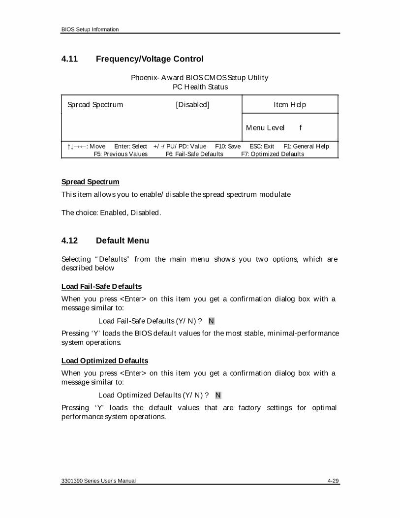
4.11 Frequency/Voltage Control
Phoenix- Award BIOS CMOS Setup UtilityPC Health Status
Spread Spectrum [Disabled] Item Help
Menu Level f
: Move Enter: Select +/-/PU/PD: Value F10: Save ESC: Exit F1: General HelpF5: Previous Values F6: Fail-Safe Defaults F7: Optimized Defaults
Spread Spectrum
This item allows you to enable/disable the spread spectrum modulate
The choice: Enabled, Disabled.
4.12 Default Menu
Selecting “Defaults” from the main menu shows you two options, which aredescribed below
Load Fail-Safe DefaultsWhen you press <Enter> on this item you get a confirmation dialog box with amessage similar to:
Load Fail-Safe Defaults (Y/N) ? NPressing ‘Y’ loads the BIOS default values for the most stable, minimal-performancesystem operations.
Load Optimized DefaultsWhen you press <Enter> on this item you get a confirmation dialog box with amessage similar to:
Load Optimized Defaults (Y/N) ? N
Pressing ‘Y’ loads the default values that are factory settings for optimalperformance system operations.
3301390 Series User s Manual 4-29

BIOS Setup Information
4.13 Supervisor/User Password Setting
You can set either supervisor or user password, or both of then. The differencesbetween are:
Set Supervisor Password: can enter and change the options of the setup menus.
Set User Password: just can only enter but do not have the right to change theoptions of the setup menus. When you select this function, the following messagewill appear at the center of the screen to assist you in creating a password.
ENTER PASSWORDType the password, up to eight characters in length, and press <Enter>. Thepassword typed now will clear any previously entered password from CMOSmemory. You will be asked to confirm the password. Type the password againand press <Enter>. You may also press <Esc> to abort the selection and not enter apassword.
To disable a password, just press <Enter> when you are prompted to enter thepassword. A message will confirm the password will be disabled. Once thepassword is disabled, the system will boot and you can enter Setup freely.
PASSWORD DISABLEDWhen a password has been enabled, you will be prompted to enter it every time youtry to enter Setup. This prevents an unauthorized person from changing any partof your system configuration.
Additionally, when a password is enabled, you can also require the BIOS to requesta password every time your system is rebooted. This would prevent unauthorizeduse of your computer.
You determine when the password is required within the BIOS Features Setup Menuand its Security option (see Section 3). If the Security option is set to “System”, thepassword will be required both at boot and at entry to Setup. If set to “Setup”,prompting only occurs when trying to enter Setup.
3301390 Series User s Manual 4-30

BIOS Setup Information
4.14 Exiting Selection
Save & Exit Setup
Pressing <Enter> on this item asks for confirmation:
Save to CMOS and EXIT (Y/N)? Y
Pressing “Y” stores the selections made in the menus in CMOS – a special section ofmemory that stays on after you turn your system off. The next time you boot yourcomputer, the BIOS configures your system according to the Setup selections storedin CMOS. After saving the values the system is restarted again.
Exit Without Saving
Pressing <Enter> on this item asks for confirmation:
Quit Without Saving (Y/N)? N
This allows you to exit Setup without storing in CMOS any change. The previousselections remain in effect. This exits the Setup utility and restarts your computer.
3301390 Series User s Manual 4-31

Troubleshooting
Chapter 5Troubleshooting
This chapter provides a few useful tips to quickly get 3301390 running withsuccess. As basic hardware installation has been addressed in Chapter 2, this chapterwill primarily focus on system integration issues, in terms of BIOS setting, and OSdiagnostics.
5.1 Hardware Quick Installation
Backplane3301390 series is a full-sized Signal Board Computer, and therefore is only able torun on PICMG PCI/ISA backplane. To know whether your backplane is PICMGPCI/ISA backplane, please contact with vendor or manufacturer.
P4 Power connector3301390 series requires power drawing from at least one or two powerconnectors (J28 and J16), depending on power mode (AT or ATX). The CPUsupplementary Power Connector (J28) has to be connected to a system all the timeno matter using AT or ATX mode. Otherwise, the system won’t boot up properly. Inaddition, the 4-pin connector (J16) is only required at ATX mode due to the fact that4-pin connector provides 5V Stand-by from the backplane to the SBC. If J16 isn’tconnected, it could also because system failed to boot up.
Figure 5-1
3301390 Series User s Manual 5-1

Troubleshooting
ATX Power Setting
This section would be more likely to introduce you how to set up ATX mode on your3301390 series. Please refer to the following instruction.
Step 1: Connect 20-pin power cable of the ATX POWER with ATX POWERCONNECTOR (20-pin) on the backplane. (Figure 5-2)
Figure 5-2
Step 2: Use 4-pin power cable to connect both ATX P/S Control Connector onbackplane and ATX Power Control (J16) on Signal Board Computer. (Figure
5-3)
Figure 5-3
3301390 Series User s Manual 5-2

Troubleshooting
Step 3: Please adjust AT/ATX Jumper on JP6 to short 3-5, 4-6 pins, then it cansupport ATX power scheme. (Figure 5-4)
Figure 5-4
Step 4: Please connect 12V Power to CPU supplementary Power Connector (J28),which shows on Figure 5-1.
Step 5: Connect TOGGLE SWITCH with J7 connector on 3301390 series (Figure 5-5), which is used to power on ATX Power Supply. Generally, the TOGGLESWITCH is located on the chassis of front panel.
Figure 5-5
3301390 Series User s Manual 5-3

Troubleshooting
AT Power SettingThis section will introduce you how to quickly and appropriately set up AT poweron your system.
Step 1: Please adjust AT/ATX Jumper on JP6 to short 1-3, 2-4 pins, then it cansupport AT power scheme. (Figure 5-6)
Figure 5-6
Note:If current Power setting is at ATX mode, please clean CMOS first before adjustingPower setting to AT mode. Otherwise, system would not boot up properly.
Step 2: Remove 4 pins power cable, and then put a jumper back on pin 3 (PS-ON)and pin 4 (GND) of backplane ATX P/S control connector. (Figure 5-7)
Figure 5-7
3301390 Series User s Manual 5-4
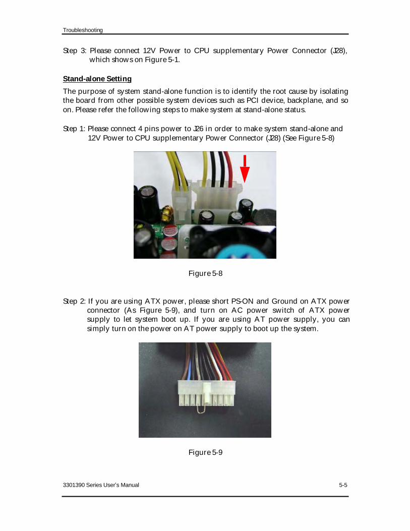
Troubleshooting
Step 3: Please connect 12V Power to CPU supplementary Power Connector (J28),which shows on Figure 5-1.
Stand-alone SettingThe purpose of system stand-alone function is to identify the root cause by isolatingthe board from other possible system devices such as PCI device, backplane, and soon. Please refer the following steps to make system at stand-alone status.
Step 1: Please connect 4 pins power to J26 in order to make system stand-alone and12V Power to CPU supplementary Power Connector (J28) (See Figure 5-8)
Figure 5-8
Step 2: If you are using ATX power, please short PS-ON and Ground on ATX powerconnector (As Figure 5-9), and turn on AC power switch of ATX powersupply to let system boot up. If you are using AT power supply, you cansimply turn on the power on AT power supply to boot up the system.
Figure 5-9
3301390 Series User s Manual 5-5

Troubleshooting
Note:In fact, different power supply has different definition of pin assignments. Therefore,please check Pin assignment on Power Supply or ask your vendor.
Unboot problemSymptom: After changing power mode from ATX to AT, my system is just not
working.
Solution: Due to ICH6 design, when you change your power mode from ATX to ATor from AT to ATX, you have to clean your CMOS in order to make yoursystem boot up properly. To clean CMOS, please short 1-2 pins on JP7 fora moment, and then change it back to its default setting. (Figure 5-10)
Figure 5-10
Symptom: keeps beeping, and no screen has shown.
Solution: In fact, each beep sound represents different definition of error message.Please refer to table as following:
Beep sounds Meaning ActionOne long beep with one DRAM error Change DRAM or reinstall itshort beepsOne long beep constantly DRAM error Change DRAM or reinstall itOne long beep with two Monitor or Display Please check Monitor connectorshort beeps Card error whether it inserts properlyBeep rapidly Power error warning Please check Power mode setting
3301390 Series User s Manual 5-6

Troubleshooting
Symptom: There is neither no beeps nor screen output.
Solution: Indeed, you shall make the SBC stand-alone to identify the root cause byisolating the board from other possible system devices such as PCI device,backplane, and so on. If the system still cannot boot up, please fill outRMA from which is provided on Global American website, and then sendback to Global American as a RMA? Besides, you also visitRMA site (http://www.GlobalAmericaninc.com) to check RMAreport if necessary.
5.2 Frequency Asking Questions
Q: How to use Standard PS/2 Keyboard and Mouse?
A: Users can adopt bracket over the J36 jumper interface which supports PS/2keyboard and mouse function on 3301390 series. (Figure 5-11)
Figure 5-11
Q: What is Serial ATA and how to use it exactly?
The Intel ® 82801FB ICH6 contains two integrated Serial ATA host controllerscapable of DMA operation on four ports. Unlike IDE bus, each Serial ATA channelcan only connect to one SATA hard disk at a time; there are total four connectors,J21, J22, J41 and J42. The installation of Serial ATA is simpler and easier than IDE,because SATA hard disk doesn’t require setting up Master and Slave, which canreduce mistake of hardware installation. All you need to do is to plug in two cablesand enable SATA in System BIOS. (The Serial ATA hard disk of installation, pleasesee Figure 5-12 as below)
3301390 Series User s Manual 5-7

Troubleshooting
Figure 5-12
After done with the installation of SATA hardware, please enter system BIOS toenable Serial ATA function. Otherwise, Serial hardware won’t be recognized. Toenable SATA function, please see as following:
System BIOSIntegrated Peripherals
On Chip IDE Device …….…………[Press enter]
On-Chip Serial ATA .…….. [Auto]
A: As matter of fact, you need to access system BIOS to enable SATA device. (Pleaserefer to SATA hard disk device installation guide)
Q: I have one IDE hard disk and one SATA hard disk. How can I assign SATAhard disk as First boot device?
A: After entering system BIOS, access Advanced BIOS Feature. And then press enterHard disk boot Priority. You will see the mode of your SATA hard disk. Select itas first boot device. Every time, when your hard disk devices have beenchanged, system BIOS will ask you to re-setup Hard disk boot priority.
Q: After inserting Compact Flash, why doesn t it work at all?
A: Compact Flash is occupied with the (Master device of Primary IDE Channel Ifthere is any device occupying this channel, please remove it or set it as a Slavedevice.
3301390 Series User s Manual 5-8

Troubleshooting
Q: I am using an ATA-66 (or 100) hard drive, how can I know that ATA-66function is enabled?
A: You need to use the 80-pin ATA-66 IDE flat cable to have this function. DuringThe Post phase, you can see ATA-66 (or 100) message while hard drive is beingdetected. Besides, after installing Microsoft series OS successfully, you also needto install ATA-66/100 driver to active ATA-66/100 function.
Q: Could 3301390 series support RAID function?
A: No, 3301390 adopts Intel ® 82801FB ICH6. From Intel spec, it doesn’t supportRaid function, only 82801FB ICH6-R support Raid function.
5.3 BIOS Setting
It is assumed that users have correctly adopted modules and connected all thedevices cables required before turning on AT or ATX power. CPU, CPU Fan, 200-pinDDR2 SDRAM, keyboard, mouse, floppy drive, IDE hard disk, printer, VGAconnector, device cables, ATX accessories are good examples that deserve attention.With no assurance of properly and correctly accommodating these modules anddevices, it is very possible to encounter system failures that result in malfunction ofany device.
To make sure that you have a successful start with 3301390 series, it isrecommended, when going with the boot-up sequence, to hit “DEL” key and enterthe BIOS setup menu to tune up a stable BIOS configuration so that you can wake upyour system far well.
Loading the default optimal settingWhen prompted with the main setup menu, please scroll down to “Load OptimalDefaults”, press “Enter” and “Y” to load in default optimal BIOS setup. This willforce your BIOS setting back to the initial factory configuration. It is recommendedto do this so you can be sure the system is running with the BIOS setting thatGlobal American has highly endorsed. As a matter of fact, users can load thedefault BIOS setting any time when system appears to be unstable in boot upsequence.
Auto Detect Hard DisksIn the BIOS => Standard CMOS setup menu, pick up any one fromPrimary/Secondary Master/Slave IDE ports, and press “Enter”. Setup the selectedIDE port and its access mode to “Auto”. This will force system to automatically pickup the IDE devices that are being connected each time system boots up.
3301390 Series User s Manual 5-9

Troubleshooting
Improper disable operationThere are too many occasions where users disable a certain device/feature in oneapplication through BIOS setting. These variables may not be set back to the originalvalues when needed. These devices/features will certainly fail to be detected.
When the above conditions happen, it is strongly recommended to check the BIOSsettings. Make sure certain items are set as they should be. These include the floppydrive, COM1/COM2 ports, Parallel port, USB ports, external cache, on-board VGAand Ethernet.
It is also very common that users would like to disable a certain device/port torelease IRQ resource. A few good examples are
Disable COM1 serial port to release IRQ #4Disable COM2 serial port to release IRQ #3Disable Parallel port to release IRQ #7Disable PS/2 mouse to release IRQ #12,Etc…
A quick review of the basic IRQ mapping is given below for your reference.
IRQ# DescriptionIRQ #0 System TimerIRQ #1 KeyboardIRQ #2 UnassignedIRQ #3 COM2IRQ #4 COM1IRQ #5 USB 1.0/1.1 UHCI and EHCI 2.0 ControllerIRQ #6 Floppy Disk ControllerIRQ #7 Parallel portIRQ #8 Real-time ClockIRQ #9 Microsoft ACPI-Compliant System
IRQ #10 Network Controller /Multimedia DeviceIRQ #11 SMbus /Primary IDE ControllerIRQ #12 Network /Display ControllerIRQ #13 Data ProcessorIRQ #14 Primary IDE ControllerIRQ #15 Unused
It is then very easy to find out which IRQ resource is ready for additionalperipherals. If IRQ resource is not enough, please disable some devices listed aboveto release further IRQ numbers.
3301390 Series User s Manual 5-10

Appendix A
System Memory Address Map (Only for 3301390 )Each On-board device in the system is assigned a set of memory addresses, whichalso can be identical of the device. The following table lists the system memoryaddress used.
Memory Area Size Device Description0000 – 003F 1K Interrupt Area0040 – 004F 0.3K BIOS Data Area0050 – 006F 0.5K System Data0070 – 0E2E 54K DOS0E2F – 0F66 4.9K Program Area0F67 – 9F7F 576K [Available]
= Conventional memory ends at 638K =9F80 – 9FFF 2K Extended BIOS AreaA000 – AFFF 64K VGA GraphicsB000 – B7FF 32K UnusedB800 – BFFF 32K VGA TextC000 – CE7F 58K Video ROMCE80 – CFFF 6K UnusedD000 – D3FF 16K ROMD400 – EEFF 108K UnusedDA4A –DFFE 22K High RAME000 – EFFF 64K Temporary Memory Area for BIOSF000 – FFFF 64K System ROM
3301390 Series User s Manual

Appendix A
System Memory Address Map (Only for 3301390 )Each On-board device in the system is assigned a set of memory addresses, whichalso can be identical of the device. The following table lists the system memoryaddress used.
Memory Area Size Device Description0000 – 003F 1K Interrupt Area0040 – 004F 0.3K BIOS Data Area0050 – 006F 0.5K System Data0070 – 0436 15K DOS0437 – 04F2 2.9K Program Area04F3 – 9F7F 618K [Available]
= Conventional memory ends at 638K =9F80 – 9FFF 2K Extended BIOS AreaA000 – AFFF 64K VGA GraphicsB000 – B7FF 32K UnusedB800 – BFFF 32K VGA TextC000 – CFFF 64K Video ROMD000 – D7FF 32K ROMD800 – DFFF 32K UnusedE000 – EFFF 64K Temporary Memory Area for BIOSF000 – FFFF 64K System ROMHMA 64K First 64K Extended
3301390 Series User s Manual

Appendix B
Interrupt Request Lines (IRQ)Peripheral devices can use interrupt request lines to notify CPU for the servicerequired. The following table shows the IRQ used by the devices on board.
IRQ# Current Use Default UseIRQ 0 SMARTDRV System TimerIRQ 1 SMARTDRV Keyboard EventIRQ 2 [Unassigned] Usable IRQIRQ 3 System ROM COM 2IRQ 4 System ROM COM 1IRQ 5 [Unassigned] Usable IRQIRQ 6 System ROM Diskette EventIRQ 7 [Unassigned] Usable IRQIRQ 8 System ROM Real-Time ClockIRQ 9 [Unassigned] Usable IRQ
IRQ 10 [Unassigned] Usable IRQIRQ 11 [Unassigned] Usable IRQIRQ 12 System ROM IBM Mouse EventIRQ 13 System ROM Coprocessor ErrorIRQ 14 System ROM Hard Disk EventIRQ 15 [Unassigned] Usable IRQ
3301390 Series User s Manual

Any advice or comments about our products and service, or anything we can help you with please don’t hesitate to contact with us. We will do our best to support your products, projects and business.
Address: Global American, Inc. 17 Hampshire Drive Hudson, NH 03051 Telephone: Toll Free U.S. Only (800) 833-8999 (603) 886-3900 FAX: (603) 886-4545 Website: http://www.globalamericaninc.com
Support: Technical Support at Global American