Embed Size (px)
Citation preview
Using the UCC29910A-730
User's Guide
Literature Number: SLUU505A
May 2011–Revised October 2011
User's GuideSLUU505A–May 2011–Revised October 2011
Buck PFC Pre-Regulator in Power Factor CorrectionApplications
1 Introduction
This EVM is to help evaluating UCC29910A buck PFC pre-regulator controller device in Power FactorCorrection (PFC) applications especially targeting notebook computer charger area with universal ACinput voltages.
2 Description
The EVM is a 100-W buck PFC pre-regulator with universal AC input between 90 VAC and 264 VAC, inputfrequency between 47 Hz and 63 Hz, and output voltage nominal 84 VDC and maximum load current 1.2 A.
2.1 Typical Applications• High Efficiency AC-DC Adapters
• Low Profile and High Density Adapters
2.2 Features• Universal Line Input AC Voltage (between 90 VAC and 264 VAC, with frequency range 47 Hz and 63 Hz)
• Regulated Output DC Voltage (84 VDC with maximum 1.2-A load current)
• Output Voltage Regulation From no Load to Full Load, and From Low Line to High Line
• High Efficiency 96% Peak and 95% at Full Load
• High Power Factor Over 0.9
• Double Sided PCB Layout
• Buck PFC Technology
• Non-Latching Input Under Voltage Protection
• Over Current Protection
• Test Points to Facilitate Device and Topology Evaluation
2 Buck PFC Pre-Regulator in Power Factor Correction Applications SLUU505A–May 2011–Revised October 2011Submit Documentation Feedback
Copyright © 2011, Texas Instruments Incorporated
www.ti.com Electrical Performance Specifications
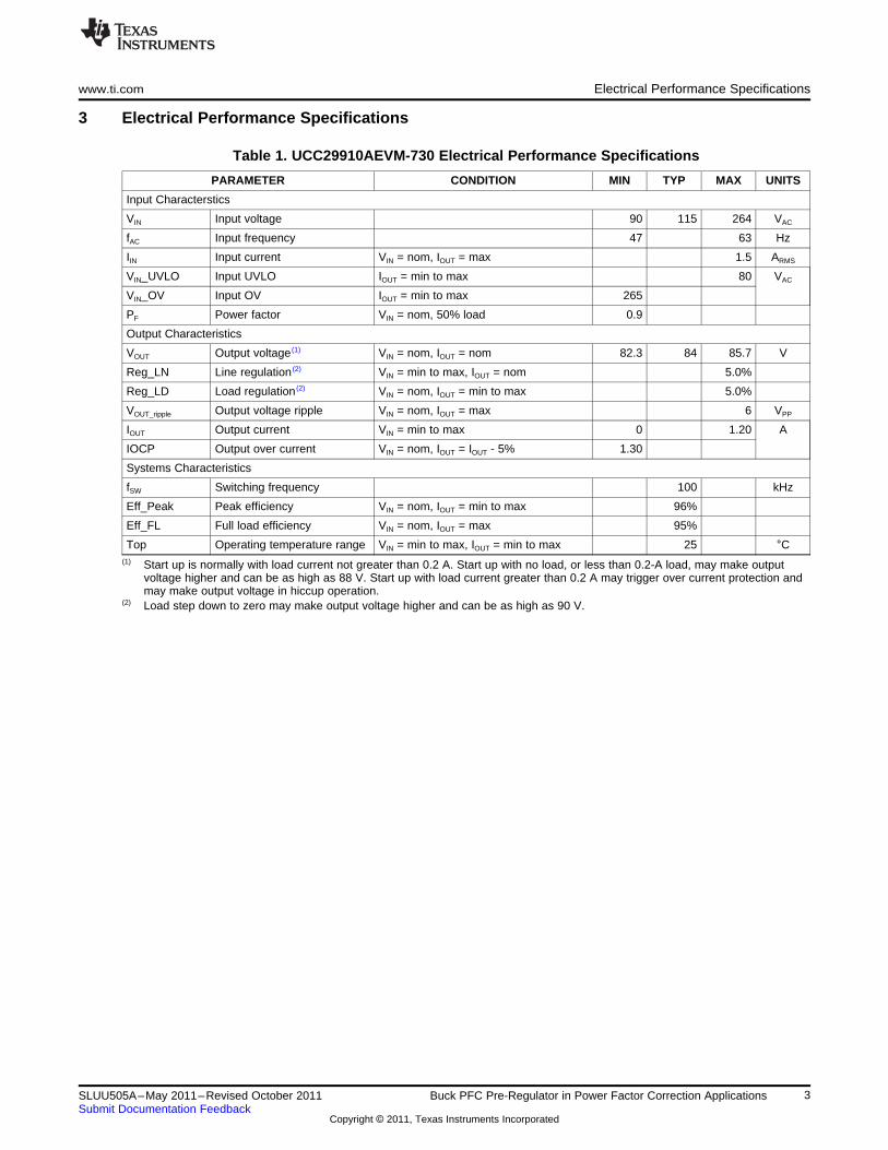
3 Electrical Performance Specifications
Table 1. UCC29910AEVM-730 Electrical Performance Specifications
PARAMETER CONDITION MIN TYP MAX UNITS
Input Characterstics
VIN Input voltage 90 115 264 VAC
fAC Input frequency 47 63 Hz
IIN Input current VIN = nom, IOUT = max 1.5 ARMS
VIN_UVLO Input UVLO IOUT = min to max 80 VAC
VIN_OV Input OV IOUT = min to max 265
PF Power factor VIN = nom, 50% load 0.9
Output Characteristics
VOUT Output voltage (1) VIN = nom, IOUT = nom 82.3 84 85.7 V
Reg_LN Line regulation (2) VIN = min to max, IOUT = nom 5.0%
Reg_LD Load regulation (2) VIN = nom, IOUT = min to max 5.0%
VOUT_ripple Output voltage ripple VIN = nom, IOUT = max 6 VPP
IOUT Output current VIN = min to max 0 1.20 A
IOCP Output over current VIN = nom, IOUT = IOUT - 5% 1.30
Systems Characteristics
fSW Switching frequency 100 kHz
Eff_Peak Peak efficiency VIN = nom, IOUT = min to max 96%
Eff_FL Full load efficiency VIN = nom, IOUT = max 95%
Top Operating temperature range VIN = min to max, IOUT = min to max 25 °C(1) Start up is normally with load current not greater than 0.2 A. Start up with no load, or less than 0.2-A load, may make output
voltage higher and can be as high as 88 V. Start up with load current greater than 0.2 A may trigger over current protection andmay make output voltage in hiccup operation.
(2) Load step down to zero may make output voltage higher and can be as high as 90 V.
3SLUU505A–May 2011–Revised October 2011 Buck PFC Pre-Regulator in Power Factor Correction ApplicationsSubmit Documentation Feedback
Copyright © 2011, Texas Instruments Incorporated
++
+
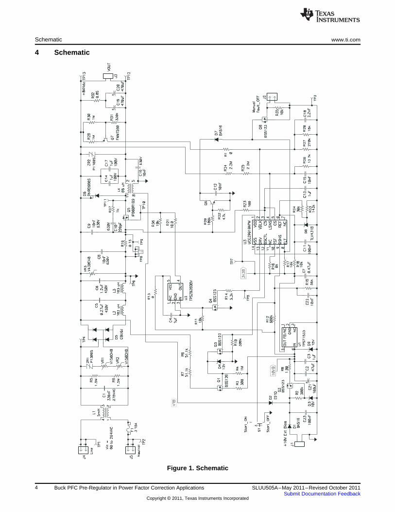
Schematic www.ti.com
4 Schematic
Figure 1. Schematic
4 Buck PFC Pre-Regulator in Power Factor Correction Applications SLUU505A–May 2011–Revised October 2011Submit Documentation Feedback
Copyright © 2011, Texas Instruments Incorporated
J3
TP1TP4
TP8
LINE
NEUTRAL
F1
L1
L2
J1
L3
TP9TP10
TP11TP6
L4
S1 J2
C1
TP13TP12
TP7
TP3
TP5TP2
D5 C5 C6
C19
C20
C21
+
+
UCC29910AEVM-730
AC SOURCE
OFF ON
+10V BIAS
SUPPLY
V1+
A1+
+-
(Electronic)
Load-1
-
-
FAN
HPA730
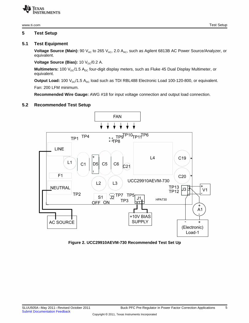
www.ti.com Test Setup
5 Test Setup
5.1 Test Equipment
Voltage Source (Main): 90 VAC to 265 VAC, 2.0 AAC, such as Agilent 6813B AC Power Source/Analyzer, orequivalent.
Voltage Source (Bias): 10 VDC/0.2 A.
Multimeters: 100 VDC/1.5 ADC four-digit display meters, such as Fluke 45 Dual Display Multimeter, orequivalent.
Output Load: 100 VDC/1.5 ADC load such as TDI RBL488 Electronic Load 100-120-800, or equivalent.
Fan: 200 LFM minimum.
Recommended Wire Gauge: AWG #18 for input voltage connection and output load connection.
5.2 Recommended Test Setup
Figure 2. UCC29910AEVM-730 Recommended Test Set Up
5SLUU505A–May 2011–Revised October 2011 Buck PFC Pre-Regulator in Power Factor Correction ApplicationsSubmit Documentation Feedback
Copyright © 2011, Texas Instruments Incorporated
Test Setup www.ti.com
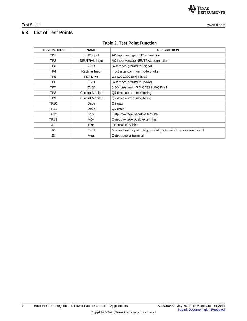
5.3 List of Test Points
Table 2. Test Point Function
TEST POINTS NAME DESCRIPTION
TP1 LINE input AC Input voltage LINE connection
TP2 NEUTRAL input AC input voltage NEUTRAL connection
TP3 GND Reference ground for signal
TP4 Rectifier Input Input after common mode choke
TP5 FET Drive U3 (UCC29910A) Pin 13
TP6 GND Reference ground for power
TP7 3V3B 3.3-V bias and U3 (UCC29910A) Pin 1
TP8 Current Monitor Q5 drain current monitoring
TP9 Current Monitor Q5 drain current monitoring
TP10 Drive Q5 gate
TP11 Drain Q5 drain
TP12 VO- Output voltage negative terminal
TP13 VO+ Output voltage positive terminal
J1 Bias External 10-V bias
J2 Fault Manual Fault Input to trigger fault protection from external circuit
J3 Vout Output power terminal
6 Buck PFC Pre-Regulator in Power Factor Correction Applications SLUU505A–May 2011–Revised October 2011Submit Documentation Feedback
Copyright © 2011, Texas Instruments Incorporated
www.ti.com Test Procedure
6 Test Procedure
Set up the EVM per Figure 2.
CAUTION
High voltage and high temperature present when the EVM is in operation!
High voltage present for some time after power down of the EVM. Check outputterminals with a voltmeter before handling the EVM!
6.1 Power Factor and Efficiency Measurement Procedure1. Check the switch S1 at ON position. If S1 is not at ON position, switch S1 to the position ON.
2. Turn on the ventilation fan and keep the fan in operation during the time of test.
3. Set the AC source voltage to 115 VAC and frequency to 60 Hz. But keep the AC source powered off
4. Prior to connecting the AC source, set the current to 2.5-A peak and 2.5-A limit. Connecting AC sourceto LINE and NEUTRAL terminals as shown in Figure 2.
5. Connect voltmeter V1 across the J3 as shown in Figure 2.
6. Connect ammeter A1 to J3 positive terminal and connect ammeter A1 to Load-1. Then connect Load-1negative terminal to J3 negative terminal.
7. Connect 10-V Bias to J1, turn on 10-V Bias.
8. Set Load-1 to constant current mode to sink 0.2 ADC and set Load-1 at 100 VDC input range beforeturning on the AC source.
9. Turn on the AC source.
10. Varying the load current from 0.2 A to 1.2 A, along with the load current variation:
(a) Read input voltage, input real power, and power factor from the AC source.
(b) Read output voltage and output current from V1 and A1.
11. Turn off the AC source.
12. Set the AC source voltage to 230 VAC and frequency to 50 Hz.
13. Repeat step 8 and 10.
NOTE: Start up is normally with load current not greater than 0.2A.
Start up with no load, or less than 0.2-A load, may make output voltage higher and can be ashigh as 88 V.
Start up with load current greater than 0.2 A may trigger over current protection and maymake output voltage in hiccup operation.
Load step down to zero may make output voltage higher and can be as high as 90 V.
6.2 Equipment Shutdown1. Shut down the AC source
2. Shut down the 10-V Bias
3. Shut down the load
4. Shut down the FAN
CAUTION
High voltage may present after power down of the EVM for some time. Checkoutput terminals with a voltmeter before handling the EVM!
7SLUU505A–May 2011–Revised October 2011 Buck PFC Pre-Regulator in Power Factor Correction ApplicationsSubmit Documentation Feedback
Copyright © 2011, Texas Instruments Incorporated
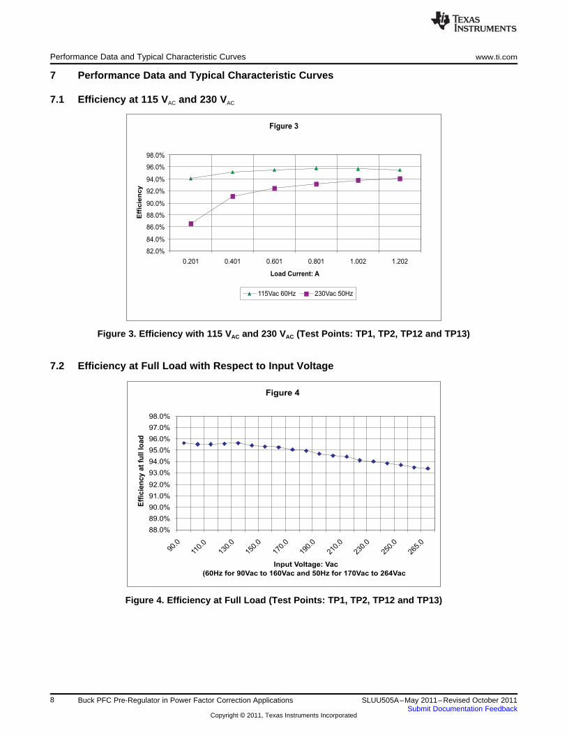
Figure 3
82.0%
84.0%
86.0%
88.0%
90.0%
92.0%
94.0%
96.0%
98.0%
0.201 0.401 0.601 0.801 1.002 1.202
Load Current: A
Effic
ien
cy
115Vac 60Hz 230Vac 50Hz
Figure 4
88.0%
89.0%
90.0%
91.0%
92.0%
93.0%
94.0%
95.0%
96.0%
97.0%
98.0%
90.0
110.
0
130.
0
150.
0
170.
0
190.
0
210.
0
230.
0
250.
0
265.
0
Input Voltage: Vac
(60Hz for 90Vac to 160Vac and 50Hz for 170Vac to 264Vac
Effic
ien
cy
at f
ull
lo
ad
Performance Data and Typical Characteristic Curves www.ti.com
7 Performance Data and Typical Characteristic Curves
7.1 Efficiency at 115 VAC and 230 VAC
Figure 3. Efficiency with 115 VAC and 230 VAC (Test Points: TP1, TP2, TP12 and TP13)
7.2 Efficiency at Full Load with Respect to Input Voltage
Figure 4. Efficiency at Full Load (Test Points: TP1, TP2, TP12 and TP13)
8 Buck PFC Pre-Regulator in Power Factor Correction Applications SLUU505A–May 2011–Revised October 2011Submit Documentation Feedback
Copyright © 2011, Texas Instruments Incorporated
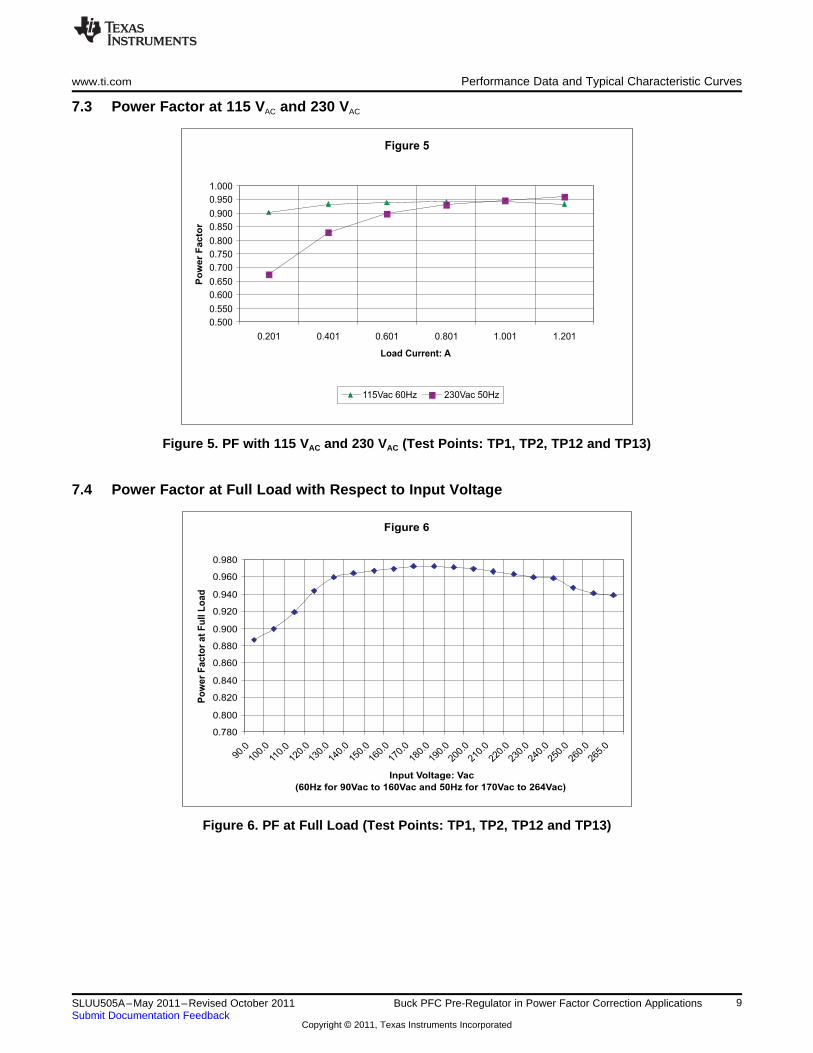
Figure 5
0.500
0.550
0.600
0.650
0.700
0.750
0.800
0.850
0.900
0.950
1.000
0.201 0.401 0.601 0.801 1.001 1.201
Load Current: A
Po
wer F
acto
r
115Vac 60Hz 230Vac 50Hz
Figure 6
0.780
0.800
0.820
0.840
0.860
0.880
0.900
0.920
0.940
0.960
0.980
90.0
100.
0
110.
0
120.
0
130.
0
140.
0
150.
0
160.
0
170.
0
180.
0
190.
0
200.
0
210.
0
220.
0
230.
0
240.
0
250.
0
260.
0
265.
0
Input Voltage: Vac
(60Hz for 90Vac to 160Vac and 50Hz for 170Vac to 264Vac)
Po
wer F
acto
r a
t F
ull L
oad
www.ti.com Performance Data and Typical Characteristic Curves
7.3 Power Factor at 115 VAC and 230 VAC
Figure 5. PF with 115 VAC and 230 VAC (Test Points: TP1, TP2, TP12 and TP13)
7.4 Power Factor at Full Load with Respect to Input Voltage
Figure 6. PF at Full Load (Test Points: TP1, TP2, TP12 and TP13)
9SLUU505A–May 2011–Revised October 2011 Buck PFC Pre-Regulator in Power Factor Correction ApplicationsSubmit Documentation Feedback
Copyright © 2011, Texas Instruments Incorporated
Input Harmonic Content
1.00
10.00
100.00
1000.00
1 3 5 7 9 11 13 15 17 19 21 23 25 27 29 31 33 35 37 39
Harmonic Number
(230Vac, 50Hz, Full Load)
Cu
rre
nt: m
Arm
s
EVM Limits
Input Harmonic Content
1.00
10.00
100.00
1000.00
1 3 5 7 9 11 13 15 17 19 21 23 25 27 29 31 33 35 37 39
Harmonic Number
(100Vac, 50Hz, Full Load)
Cu
rre
nt: m
Arm
s
EVM Limits
Performance Data and Typical Characteristic Curves www.ti.com
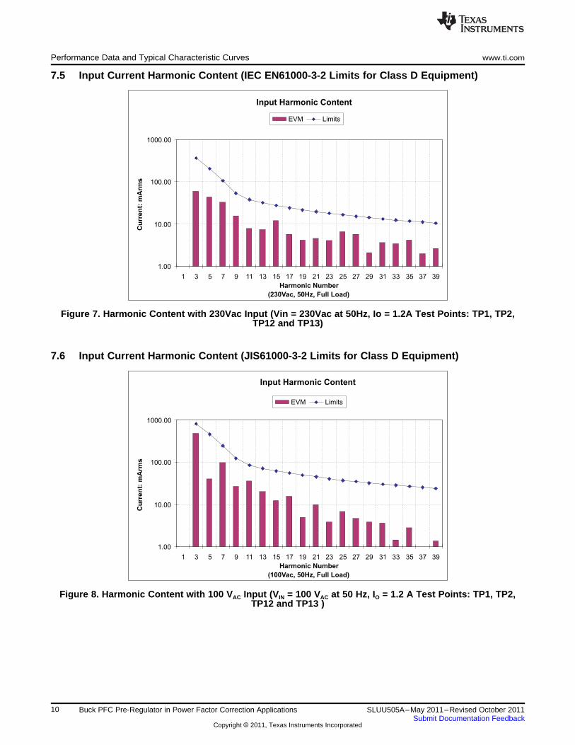
7.5 Input Current Harmonic Content (IEC EN61000-3-2 Limits for Class D Equipment)
Figure 7. Harmonic Content with 230Vac Input (Vin = 230Vac at 50Hz, Io = 1.2A Test Points: TP1, TP2,TP12 and TP13)
7.6 Input Current Harmonic Content (JIS61000-3-2 Limits for Class D Equipment)
Figure 8. Harmonic Content with 100 VAC Input (VIN = 100 VAC at 50 Hz, IO = 1.2 A Test Points: TP1, TP2,TP12 and TP13 )
10 Buck PFC Pre-Regulator in Power Factor Correction Applications SLUU505A–May 2011–Revised October 2011Submit Documentation Feedback
Copyright © 2011, Texas Instruments Incorporated
www.ti.com Performance Data and Typical Characteristic Curves
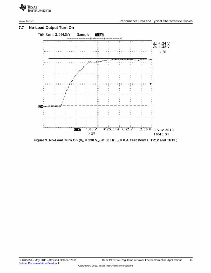
7.7 No-Load Output Turn On
Figure 9. No-Load Turn On (VIN = 230 VAC at 50 Hz, IO = 0 A Test Points: TP12 and TP13 )
11SLUU505A–May 2011–Revised October 2011 Buck PFC Pre-Regulator in Power Factor Correction ApplicationsSubmit Documentation Feedback
Copyright © 2011, Texas Instruments Incorporated
Performance Data and Typical Characteristic Curves www.ti.com
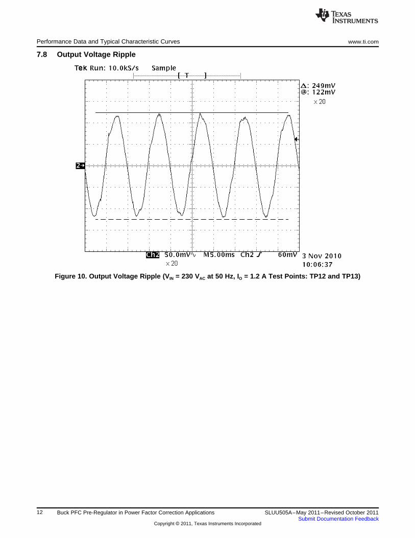
7.8 Output Voltage Ripple
Figure 10. Output Voltage Ripple (VIN = 230 VAC at 50 Hz, IO = 1.2 A Test Points: TP12 and TP13)
12 Buck PFC Pre-Regulator in Power Factor Correction Applications SLUU505A–May 2011–Revised October 2011Submit Documentation Feedback
Copyright © 2011, Texas Instruments Incorporated
www.ti.com Performance Data and Typical Characteristic Curves
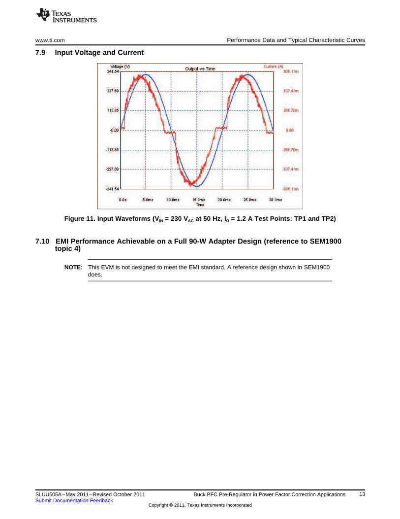
7.9 Input Voltage and Current
Figure 11. Input Waveforms (VIN = 230 VAC at 50 Hz, IO = 1.2 A Test Points: TP1 and TP2)
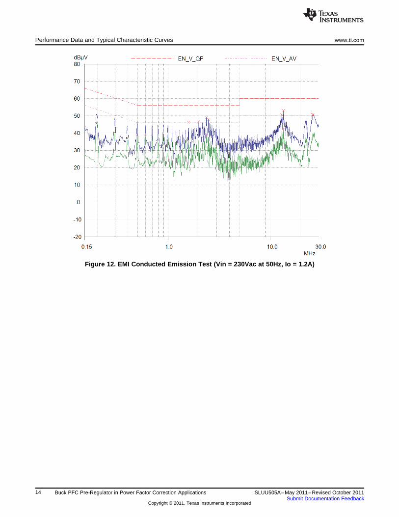
7.10 EMI Performance Achievable on a Full 90-W Adapter Design (reference to SEM1900topic 4)
NOTE: This EVM is not designed to meet the EMI standard. A reference design shown in SEM1900does.
13SLUU505A–May 2011–Revised October 2011 Buck PFC Pre-Regulator in Power Factor Correction ApplicationsSubmit Documentation Feedback
Copyright © 2011, Texas Instruments Incorporated
Performance Data and Typical Characteristic Curves www.ti.com
Figure 12. EMI Conducted Emission Test (Vin = 230Vac at 50Hz, Io = 1.2A)
14 Buck PFC Pre-Regulator in Power Factor Correction Applications SLUU505A–May 2011–Revised October 2011Submit Documentation Feedback
Copyright © 2011, Texas Instruments Incorporated
L4
J4
J5
www.ti.com EVM Assembly Drawing and PCB layout
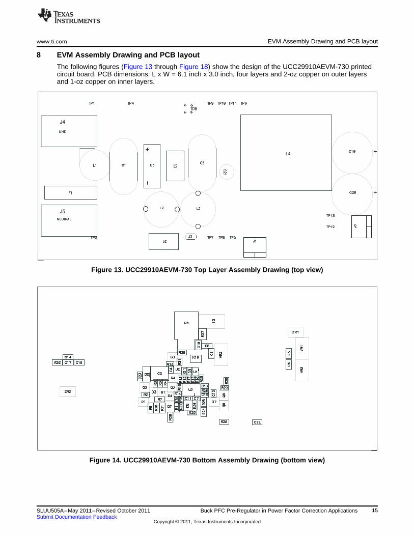
8 EVM Assembly Drawing and PCB layout
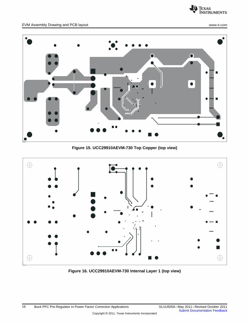
The following figures (Figure 13 through Figure 18) show the design of the UCC29910AEVM-730 printedcircuit board. PCB dimensions: L x W = 6.1 inch x 3.0 inch, four layers and 2-oz copper on outer layersand 1-oz copper on inner layers.
Figure 13. UCC29910AEVM-730 Top Layer Assembly Drawing (top view)
Figure 14. UCC29910AEVM-730 Bottom Assembly Drawing (bottom view)
15SLUU505A–May 2011–Revised October 2011 Buck PFC Pre-Regulator in Power Factor Correction ApplicationsSubmit Documentation Feedback
Copyright © 2011, Texas Instruments Incorporated
EVM Assembly Drawing and PCB layout www.ti.com
Figure 15. UCC29910AEVM-730 Top Copper (top view)
Figure 16. UCC29910AEVM-730 Internal Layer 1 (top view)
16 Buck PFC Pre-Regulator in Power Factor Correction Applications SLUU505A–May 2011–Revised October 2011Submit Documentation Feedback
Copyright © 2011, Texas Instruments Incorporated
www.ti.com EVM Assembly Drawing and PCB layout
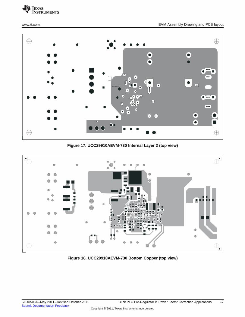
Figure 17. UCC29910AEVM-730 Internal Layer 2 (top view)
Figure 18. UCC29910AEVM-730 Bottom Copper (top view)
17SLUU505A–May 2011–Revised October 2011 Buck PFC Pre-Regulator in Power Factor Correction ApplicationsSubmit Documentation Feedback
Copyright © 2011, Texas Instruments Incorporated
List of Materials www.ti.com
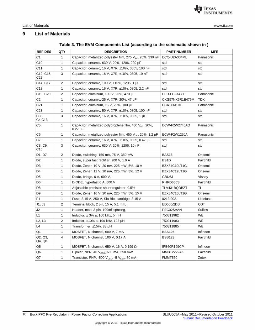
9 List of Materials
Table 3. The EVM Components List (according to the schematic shown in )
REF DES QTY DESCRIPTION PART NUMBER MFR
C1 1 Capacitor, metallized polyester film, 275 VAC, 20%, 330 nF ECQ-U2A334ML Panasonic
C10 1 Capacitor, ceramic, 630 V, 20%, 1206, 220 pF std std
C11 1 Capacitor, ceramic, 16 V, X7R, ±10%, 0805, 100 nF std std
C12, C15, 3 Capacitor, ceramic, 16 V, X7R, ±10%, 0805, 10 nF std stdC22
C14, C17 2 Capacitor, ceramic, 100 V, ±10%, 1206, 1 µF std std
C18 1 Capacitor, ceramic, 16 V, X7R, ±10%, 0805, 2.2 nF std std
C19, C20 2 Capacitor, aluminum, 100 V, 20%, 470 µF EEU-FC2A471 Panasonic
C2 1 Capacitor, ceramic, 25 V, X7R, 20%, 47 µF CKG57NX5R1E476M TDK
C21 1 Capacitor, aluminum, 16 V, 20%, 100 µF ECA1CM101 Panasonic
C23 1 Capacitor, ceramic, 50 V, X7R, ±10%, 0805, 100 nF std std
C3, 3 Capacitor, ceramic, 16 V, X7R, ±10%, 0805, 1 µF std stdC4,C13
C5 1 Capacitor, metallized polyproplene film, 450 VDC, 20%, ECW-F2W274JAQ Panasonic0.27 µF
C6 1 Capacitor, metallized polyester film, 450 VDC, 20%, 1.2 µF ECW-F2W125JA Panasonic
C7 1 Capacitor, ceramic, 16 V, X7R, ±10%, 0805, 0.47 µF std std
C8, C9, 3 Capacitor, ceramic, 630 V, 20%, 1206, 10 nF std stdC16
D1, D7 2 Diode, switching, 150 mA, 75 V, 350 mW BAS16 Onsemi
D2 1 Diode, super fast rectifier, 200 V, 1.0 A ES1D Fairchild
D3 1 Diode, Zener, 10 V, 20 mA, 225 mW, 5%, 10 V BZX84C10LT1G Onsemi
D4 1 Diode, Zener, 12 V, 20 mA, 225 mW, 5%, 12 V BZX84C12LT1G Onsemi
D5 1 Diode, bridge, 6 A, 600 V, GBU6J Vishay
D6 1 DIODE, hyperfast 6 A, 600 V RHRD660S Fairchild
D8 1 Adjustable precision shunt regulator, 0.5% TLV431BQDBZT TI
D9 1 Diode, Zener, 10 V, 20 mA, 225 mW, 5%, 15 V BZX84C15LT1G Onsemi
F1 1 Fuse, 3.15 A, 250 V, Slo-Blo, cartridge, 3.15 A 0213 002. Littlefuse
J1, J3 2 Terminal block, 2 pin, 15 A, 5.1 mm, ED500/2DS OST
J2 1 Header, male 2-pin, 100mil spacing, PEC02SAAN Sullins
L1 1 Inductor, ± 3% at 100 kHz, 5 mH 750311982 WE
L2, L3 2 Inductor, ±10% at 100 kHz, 103 µH 750311983 WE
L4 1 Transformer, ±15%, 88 µH 750311885 WE
Q1 1 MOSFET, N-channel, 600 V, 7 mA BSS126 Infineon
Q2, Q3, 4 MOSFET, N-channel, 100 V, 0.17 A BSS123 FairchildQ4, Q8
Q5 1 MOSFET, N-channel, 650 V, 16 A, 0.199 Ω IPB60R199CP Infineon
Q6 1 Bipolar, NPN, 40 VCEO, 600 mA, 350 mW MMBT2222AK Fairchild
Q7 1 Transistor, PNP, -500 VCEO, -5 VEBO, 50 mA FMMT560 Zetex
18 Buck PFC Pre-Regulator in Power Factor Correction Applications SLUU505A–May 2011–Revised October 2011Submit Documentation Feedback
Copyright © 2011, Texas Instruments Incorporated
www.ti.com List of Materials
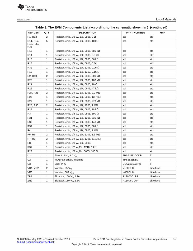
Table 3. The EVM Components List (according to the schematic shown in ) (continued)
REF DES QTY DESCRIPTION PART NUMBER MFR
R1, R13 2 Resistor, chip, 1/8 W, 1%, 0805, 0 Ω std std
R11, R17, 5 Resistor, chip, 1/8 W, 1%, 0805, 10 kΩ std stdR18, R35,R36
R12 1 Resistor, chip, 1/8 W, 1%, 0805, 680 kΩ std std
R14 1 Resistor, chip, 1/8 W, 1%, 0805, 3.3 kΩ std std
R15 1 Resistor, chip, 1/8 W, 1%, 0805, 56 kΩ std std
R16 1 Resistor, chip, 1/8 W, 1%, 0805, 0 Ω std std
R32 1 Resistor, chip, 1/4 W, 1%, 1206, 0.05 Ω std std
R19 1 Resistor, chip, 1/2 W, 1%, 1210, 0.15 Ω std std
R2, R10 2 Resistor, chip, 1/8 W, 1%, 0805, 300 kΩ std std
R20 1 Resistor, chip, 1/8 W, 1%, 0805, 100 kΩ std std
R21 1 Resistor, chip, 1/8 W, 1%, 0805, 10 Ω std std
R22 1 Resistor, chip, 1/8 W, 1%, 0805, 47 kΩ std std
R24, R25 2 Resistor, chip, 1/4 W, 1%, 1206, 2.2 MΩ std std
R26 1 Resistor, chip, 1/8 W, 1%, 0805, 13.7 kΩ std std
R27 1 Resistor, chip, 1/8 W, 1%, 0805, 270 kΩ std std
R28, R30 2 Resistor, chip, 1/4 W, 1%, 1206, 1 MΩ std std
R29 1 Resistor, chip, 1/8 W, 1%, 0805, 18 kΩ std std
R3 1 Resistor, chip, 1/8 W, 1%, 0805, 390 Ω std std
R31 1 Resistor, chip, 1/4 W, 1%, 1206, 330 kΩ std std
R33 1 Resistor, chip, 1/8 W, 1%, 0805, 143 kΩ std std
R34 1 Resistor, chip, 1/8 W, 1%, 0805, 30 kΩ std std
R4 1 Resistor, chip, 1/8 W, 1%, 0805, 1 MΩ std std
R5, R6 2 Resistor, chip, 1/4 W, 1%, 1206, 1.5 MΩ std std
R7, R9 2 Resistor, chip, 1/4 W, 1%, 1206, 51.1 kΩ std std
R8 1 Resistor, chip, 1/8 W, 1%, 0805, std std
R37 1 Resistor, chip, 1/2 W,1%, 1210, 1 kΩ std std
R23 1 Resistor, chip, 1/8 W,1%, 0805, 100 Ω std std
U1 1 50-mA LDO, 3.0 VO TPS71533DCKR TI
U2 1 MOSFET driver, inverting TPS2828DBV TI
U3 1 Buck PFC UCC29910APW TI
VR1, VR2 2 Varistor, 95 VAC V150CH8 Littelfuse
VR3 1 Varistor, 369 VDC V430CH8 Littelfuse
ZR1 1 Sidactor, 160 VS, 2.2A P1300SCLRP Littelfuse
ZR2 1 Sidactor, 130 VS, 2.2A P1100SCLRP Littelfuse
19SLUU505A–May 2011–Revised October 2011 Buck PFC Pre-Regulator in Power Factor Correction ApplicationsSubmit Documentation Feedback
Copyright © 2011, Texas Instruments Incorporated
Evaluation Board/Kit Important Notice
Texas Instruments (TI) provides the enclosed product(s) under the following conditions:
This evaluation board/kit is intended for use for ENGINEERING DEVELOPMENT, DEMONSTRATION, OR EVALUATIONPURPOSES ONLY and is not considered by TI to be a finished end-product fit for general consumer use. Persons handling theproduct(s) must have electronics training and observe good engineering practice standards. As such, the goods being provided arenot intended to be complete in terms of required design-, marketing-, and/or manufacturing-related protective considerations,including product safety and environmental measures typically found in end products that incorporate such semiconductorcomponents or circuit boards. This evaluation board/kit does not fall within the scope of the European Union directives regardingelectromagnetic compatibility, restricted substances (RoHS), recycling (WEEE), FCC, CE or UL, and therefore may not meet thetechnical requirements of these directives or other related directives.
Should this evaluation board/kit not meet the specifications indicated in the User’s Guide, the board/kit may be returned within 30days from the date of delivery for a full refund. THE FOREGOING WARRANTY IS THE EXCLUSIVE WARRANTY MADE BYSELLER TO BUYER AND IS IN LIEU OF ALL OTHER WARRANTIES, EXPRESSED, IMPLIED, OR STATUTORY, INCLUDINGANY WARRANTY OF MERCHANTABILITY OR FITNESS FOR ANY PARTICULAR PURPOSE.
The user assumes all responsibility and liability for proper and safe handling of the goods. Further, the user indemnifies TI from allclaims arising from the handling or use of the goods. Due to the open construction of the product, it is the user’s responsibility totake any and all appropriate precautions with regard to electrostatic discharge.
EXCEPT TO THE EXTENT OF THE INDEMNITY SET FORTH ABOVE, NEITHER PARTY SHALL BE LIABLE TO THE OTHERFOR ANY INDIRECT, SPECIAL, INCIDENTAL, OR CONSEQUENTIAL DAMAGES.
TI currently deals with a variety of customers for products, and therefore our arrangement with the user is not exclusive.
TI assumes no liability for applications assistance, customer product design, software performance, or infringement ofpatents or services described herein.
Please read the User’s Guide and, specifically, the Warnings and Restrictions notice in the User’s Guide prior to handling theproduct. This notice contains important safety information about temperatures and voltages. For additional information on TI’senvironmental and/or safety programs, please contact the TI application engineer or visit www.ti.com/esh.
No license is granted under any patent right or other intellectual property right of TI covering or relating to any machine, process, orcombination in which such TI products or services might be or are used.
FCC Warning
This evaluation board/kit is intended for use for ENGINEERING DEVELOPMENT, DEMONSTRATION, OR EVALUATIONPURPOSES ONLY and is not considered by TI to be a finished end-product fit for general consumer use. It generates, uses, andcan radiate radio frequency energy and has not been tested for compliance with the limits of computing devices pursuant to part 15of FCC rules, which are designed to provide reasonable protection against radio frequency interference. Operation of thisequipment in other environments may cause interference with radio communications, in which case the user at his own expensewill be required to take whatever measures may be required to correct this interference.
EVM Warnings and Restrictions
It is important to operate this EVM within the input voltage range of 90 VAC to 264 VAC and the output voltage range of 83 VDC to87 VDC .
Exceeding the specified input range may cause unexpected operation and/or irreversible damage to the EVM. If there arequestions concerning the input range, please contact a TI field representative prior to connecting the input power.
Applying loads outside of the specified output range may result in unintended operation and/or possible permanent damage to theEVM. Please consult the EVM User's Guide prior to connecting any load to the EVM output. If there is uncertainty as to the loadspecification, please contact a TI field representative.
During normal operation, some circuit components may have case temperatures greater than 50° C. The EVM is designed tooperate properly with certain components above 50° C as long as the input and output ranges are maintained. These componentsinclude but are not limited to linear regulators, switching transistors, pass transistors, and current sense resistors. These types ofdevices can be identified using the EVM schematic located in the EVM User's Guide. When placing measurement probes nearthese devices during operation, please be aware that these devices may be very warm to the touch.
Mailing Address: Texas Instruments, Post Office Box 655303, Dallas, Texas 75265Copyright © 2011, Texas Instruments Incorporated
IMPORTANT NOTICE
Texas Instruments Incorporated and its subsidiaries (TI) reserve the right to make corrections, modifications, enhancements, improvements,and other changes to its products and services at any time and to discontinue any product or service without notice. Customers shouldobtain the latest relevant information before placing orders and should verify that such information is current and complete. All products aresold subject to TI’s terms and conditions of sale supplied at the time of order acknowledgment.
TI warrants performance of its hardware products to the specifications applicable at the time of sale in accordance with TI’s standardwarranty. Testing and other quality control techniques are used to the extent TI deems necessary to support this warranty. Except wheremandated by government requirements, testing of all parameters of each product is not necessarily performed.
TI assumes no liability for applications assistance or customer product design. Customers are responsible for their products andapplications using TI components. To minimize the risks associated with customer products and applications, customers should provideadequate design and operating safeguards.
TI does not warrant or represent that any license, either express or implied, is granted under any TI patent right, copyright, mask work right,or other TI intellectual property right relating to any combination, machine, or process in which TI products or services are used. Informationpublished by TI regarding third-party products or services does not constitute a license from TI to use such products or services or awarranty or endorsement thereof. Use of such information may require a license from a third party under the patents or other intellectualproperty of the third party, or a license from TI under the patents or other intellectual property of TI.
Reproduction of TI information in TI data books or data sheets is permissible only if reproduction is without alteration and is accompaniedby all associated warranties, conditions, limitations, and notices. Reproduction of this information with alteration is an unfair and deceptivebusiness practice. TI is not responsible or liable for such altered documentation. Information of third parties may be subject to additionalrestrictions.
Resale of TI products or services with statements different from or beyond the parameters stated by TI for that product or service voids allexpress and any implied warranties for the associated TI product or service and is an unfair and deceptive business practice. TI is notresponsible or liable for any such statements.
TI products are not authorized for use in safety-critical applications (such as life support) where a failure of the TI product would reasonablybe expected to cause severe personal injury or death, unless officers of the parties have executed an agreement specifically governingsuch use. Buyers represent that they have all necessary expertise in the safety and regulatory ramifications of their applications, andacknowledge and agree that they are solely responsible for all legal, regulatory and safety-related requirements concerning their productsand any use of TI products in such safety-critical applications, notwithstanding any applications-related information or support that may beprovided by TI. Further, Buyers must fully indemnify TI and its representatives against any damages arising out of the use of TI products insuch safety-critical applications.
TI products are neither designed nor intended for use in military/aerospace applications or environments unless the TI products arespecifically designated by TI as military-grade or "enhanced plastic." Only products designated by TI as military-grade meet militaryspecifications. Buyers acknowledge and agree that any such use of TI products which TI has not designated as military-grade is solely atthe Buyer's risk, and that they are solely responsible for compliance with all legal and regulatory requirements in connection with such use.
TI products are neither designed nor intended for use in automotive applications or environments unless the specific TI products aredesignated by TI as compliant with ISO/TS 16949 requirements. Buyers acknowledge and agree that, if they use any non-designatedproducts in automotive applications, TI will not be responsible for any failure to meet such requirements.
Following are URLs where you can obtain information on other Texas Instruments products and application solutions:
Products Applications
Audio www.ti.com/audio Communications and Telecom www.ti.com/communications
Amplifiers amplifier.ti.com Computers and Peripherals www.ti.com/computers
Data Converters dataconverter.ti.com Consumer Electronics www.ti.com/consumer-apps
DLP® Products www.dlp.com Energy and Lighting www.ti.com/energy
DSP dsp.ti.com Industrial www.ti.com/industrial
Clocks and Timers www.ti.com/clocks Medical www.ti.com/medical
Interface interface.ti.com Security www.ti.com/security
Logic logic.ti.com Space, Avionics and Defense www.ti.com/space-avionics-defense
Power Mgmt power.ti.com Transportation and Automotive www.ti.com/automotive
Microcontrollers microcontroller.ti.com Video and Imaging www.ti.com/video
RFID www.ti-rfid.com
OMAP Mobile Processors www.ti.com/omap
Wireless Connectivity www.ti.com/wirelessconnectivity
TI E2E Community Home Page e2e.ti.com
Mailing Address: Texas Instruments, Post Office Box 655303, Dallas, Texas 75265Copyright © 2011, Texas Instruments Incorporated