Embed Size (px)
Citation preview

IRDC3843A
02/09/101
USER GUIDE FOR IR3843A EVALUATION BOARDDouble Sided PCB
DESCRIPTION
The IR3843A is a synchronous buck converter, providing a compact, high performance and flexible solution in a small 5mmx6mm Power QFN package.
Key features offered by the IR3843A include programmable soft-start ramp, precision 0.7V reference voltage, Power Good,thermal protection, programmable switching frequency, Sequence input, Enable input, input under-voltage lockout for proper start-up, and pre-bias start-up.
An output over-current protection function is implemented by sensing the voltage developed across the on-resistance of the synchronous rectifier MOSFET for optimum cost and performance.
This user guide contains the schematic and bill of materials for the IR3843A evaluation board. The guide describes operation and use of the evaluation board itself. Detailed application information for IR3843A is available in the IR3843A data sheet.
BOARD FEATURES
• Vin = +12V (13.2V Max)
• Vcc=+5V (5.5V Max)
• Vout = +1.8V @ 0- 3A
• Fs=600kHz
• L= 2.2uH
• Cin= 1x10uF (ceramic 1206)
• Cout= 3x22uF (ceramic 0805)
SupIRBuckTM

IRDC3843A
02/09/102
A well regulated +12V input supply should be connected to VIN+ and VIN-. A maximum 3A load should be connected to VOUT+ and VOUT-. The connection diagram is shown in Fig. 1 and inputs and outputs of the board are listed in Table I.
IR3843A has two input supplies, one for biasing (Vcc) and the other as input voltage (Vin). Separate supplies should be applied to these inputs. Vcc input should be a well regulated 4.5V-5.5V supply and it would be connected to Vcc+ and Vcc-.
CONNECTIONS and OPERATING INSTRUCTIONS
LAYOUTThe PCB is a 4-layer board. All of layers are 2 Oz. copper. It is a double sided board with components mounted on both sides.
Power supply decoupling capacitors, the Bootstrap capacitor and feedback components are located close to IR3843A. The feedback resistors are connected to the output voltage at the point of regulation and are located close to the SupIRBuck. To improve efficiency, the circuit board is designed to minimize the length of the on-board power ground current path.
Table I. Connections
Sequence InputSeq.
Vout (+1.8V)VOUT+
Ground for Vcc inputVcc-
Vcc inputVcc+
EnableEnable
Power Good SignalPGood
Ground of VoutVOUT-
Ground of VinVIN-
Vin (+12V)VIN+
Signal NameConnection

IRDC3843A
02/09/103
Connection Diagram
Fig. 1: Connection diagram of IR384xA evaluation boards
Vin
PGood Vo
GND
GND
Enable
SS
Seq
AGND
Vcc
GNDTOP SIDE
BOTTOM SIDE
IRDC3843A
02/09/104
Fig. 2: Board layout, top overlay
Fig. 3: Board layout, bottom overlay (rear view)

IRDC3843A
02/09/105
Fig. 4: Board layout, mid-layer I.
Fig. 5: Board layout, mid-layer II.

IRDC3843A
02/09/106
Fig.
6:
Sche
mat
ic o
f the
IR
3843
A e
valu
atio
n bo
ard
Vou
t-1
Seq. 1
Vin
(+12
V)
C14
0.1u
F
Vcc
-
1
C10
0.1u
F
L1
2.2
uH
C24
0.1u
FC
26
8.2n
F
C13
1uF
R19
7.5K
SS 1
Vou
t (+
1.8V
)
Vcc
+
1C
210
uF
R9
23.7
K
R1
2.74
K
C3
N/S
R16
0
R3
3.16
k
R4
130
R2
4.99
K
C15
22uF
R6
20
C16 22
uFC
17 22uF
R12
2.2
6K
C18
N/S
VC
C
U1
IR38
43A
Enable14
Boot13
AGnd215
SW11
PGood8
CO
MP
3
OC
set
7P
Gnd
10SS
6
seq
1
FB2
AGnd
14
Vcc9
Vin
12
Rt
5
Ceramic cap 16V 10uF 1206
A
1
B
1
GN
D
1
R18
49.9
K
Enab
le
1
VC
C
C8
2200
pF
C7
0.1u
F
VCC
R20
N/S
R17
10.0
KPG
ood
1
C11 180p
F
Vin
+1
Vin
-1
Vou
t+1

IRDC3843A
02/09/107
Bill of Materials
IR3843AMPbFInternational
Rectifier3A SupIRBuck, PQFN 5x6mmIR3843AU1122
Not usedR2021
MCR03EZPFX7501Rohm0603,1/10W,1%7.5kR19120
MCR03EZPFX4992Rohm0603,1/10 W,1%49.9kR18119
MCR03EZPFX1002Rohm0603,1/10 W,1%10KR17118
MCR03EZPFX2261Rohm0603,1/10 W,1%2.26KR12117
CRCW06030000Z0EAVishay/Dale0603,1/10 W,5%0R16 116
MCR03EZPFX2372Rohm0603,1/10W,1%23.7KR9115
CRCW060320R0FKEAVishay/Dale0603,1/10 W,1%20R6114
ERJ-3EKF1300VPanasonic0603,1/10W,1%130R4113
MCR03EZPFX3161Rohm0603,1/10W,1%3.16kR3112
MCR03EZPFX4991Rohm0603,1/10W,1%4.99kR2111
MCR03EZPFX2741Rohm0603,1/10W,1%2.74kR1110
PCMB065T-2R2MSCyntec7.05*6.6*4.8mm,12.5mΩ max2.2uHL119
ECJ-1VB1H822KPanasonic0603, 50V, X7R, 10%8200pFC2618
Not usedC3,C187
ECJ-2FB0J226MPanasonic0805, 6.3V, X5R, 20%22uFC15 C16 C1736
GRM188R61C105KA93BMurata16V, 0603, X5R, 10%1uFC1315
GRM1885C1H181JA01DMurata50V, 0603, NP0, 5%180pFC1114
ECJ-1VB1H222KPanasonic0603,50V,X7R, 10%2200pFC813
ECJ-1VB1E104KPanasonic0603, 25V, X7R, 10%0.1uFC7 C14 C24 C10 42
ECJ-3YX1C106KPanasonic - ECG10uF,1206,16V, X7R, 20%10uFC2 11
Part NumberManufacturerDescriptionValuePart ReferenceQuantit
yItem
IRDC3843A
02/09/108
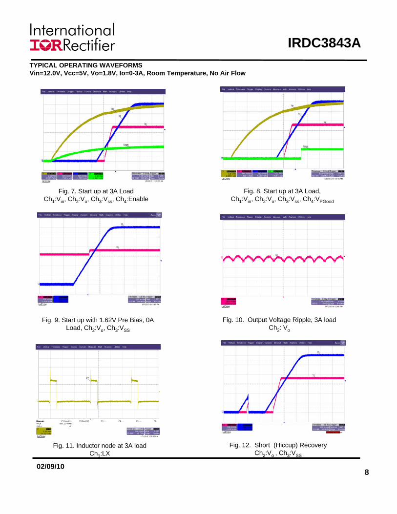
TYPICAL OPERATING WAVEFORMSVin=12.0V, Vcc=5V, Vo=1.8V, Io=0-3A, Room Temperature, No Air Flow
Fig. 11. Inductor node at 3A loadCh1:LX
Fig. 12. Short (Hiccup) RecoveryCh2:Vo , Ch3:VSS
Fig. 10. Output Voltage Ripple, 3A load Ch2: Vo
Fig. 9. Start up with 1.62V Pre Bias, 0A Load, Ch2:Vo, Ch3:VSS
Fig. 8. Start up at 3A Load, Ch1:Vin, Ch2:Vo, Ch3:Vss, Ch4:VPGood
Fig. 7. Start up at 3A LoadCh1:Vin, Ch2:Vo, Ch3:Vss, Ch4:Enable

IRDC3843A
02/09/109
TYPICAL OPERATING WAVEFORMSVin=12V, Vcc=5V, Vo=1.8V, Io=0-3A, Room Temperature, No Air Flow
Fig. 13. Transient Response, 1.5A to 3A step 2.5A/μsCh2:Vo

IRDC3843A
02/09/1010
TYPICAL OPERATING WAVEFORMSVin=12V, Vcc=5V, Vo=1.8V, Io=3A, Room Temperature, No Air Flow
Fig. 14. Bode Plot at 3A load shows a bandwidth of 83.8KHz and phase margin of 59.8°

IRDC3843A
02/09/1011
Fig.16: Power loss versus load current
Fig.15: Efficiency versus load current
TYPICAL OPERATING WAVEFORMSVin=12V, Vcc=5V, Vo=1.8V, Io=0- 3A, Room Temperature, No Air Flow
IR3843A
80
82
84
86
88
90
92
0.3 0.6 0.9 1.2 1.5 1.8 2.1 2.4 2.7 3
Iout(A)
Effic
ienc
y(%
)
IR3843A
0.000
0.100
0.200
0.300
0.400
0.500
0.600
0.700
0.3 0.6 0.9 1.2 1.5 1.8 2.1 2.4 2.7 3
Iout(A)
Pow
er D
issi
patio
n(W
)

IRDC3843A
02/09/1012
THERMAL IMAGEVin=12V, Vcc=5V, Vo=1.8V, Io=3A, Room Temperature, No Air Flow
Fig. 17: Thermal Image at 3A loadTest points 1 and 2 are IR3843A and inductor, respectively.

IRDC3843A
02/09/10
PCB Metal and Components PlacementLead lands (the 11 IC pins) width should be equal to nominal part lead width. The minimum lead to lead spacing should be ≥ 0.2mm to minimize shorting.
Lead land length should be equal to maximum part lead length + 0.3 mm outboard extension. The outboard extension ensures a large and inspectable toe fillet.
Pad lands (the 4 big pads other than the 11 IC pins) length and width should be equal to maximum part pad length and width. However, the minimum metal to metal spacing should be no less than 0.17mm for 2 oz. Copper; no less than 0.1mm for 1 oz. Copper and no less than 0.23mm for 3 oz. Copper.

IRDC3843A
02/09/10
Solder ResistIt is recommended that the lead lands are Non Solder Mask Defined (NSMD). The solder resist should be pulled away from the metal lead lands by a minimum of 0.025mm to ensure NSMD pads.
The land pad should be Solder Mask Defined (SMD), with a minimum overlap of the solder resist onto the copper of 0.05mm to accommodate solder resist misalignment.
Ensure that the solder resist in-between the lead lands and the pad land is ≥ 0.15mm due to the high aspect ratio of the solder resist strip separating the lead lands from the pad land.

IRDC3843A
02/09/10
Stencil Design• The Stencil apertures for the lead lands should be approximately 80% of the area of the
lead lads. Reducing the amount of solder deposited will minimize the occurrences of lead shorts. If too much solder is deposited on the center pad the part will float and the lead lands will be open.
• The maximum length and width of the land pad stencil aperture should be equal to the solder resist opening minus an annular 0.2mm pull back to decrease the incidence of shorting the center land to the lead lands when the part is pushed into the solder paste.

IRDC3843A
02/09/10
IR WORLD HEADQUARTERS: 233 Kansas St., El Segundo, California 90245, USA Tel: (320) 252-7105TAC Fax: (320) 252-7903
This product has been designed and qualified for the Consumer marketVisit us at www.irf.com for sales contact information
Data and specifications subject to change without notice. 01/10
BOTTOM VIEW